Embed Size (px)
Citation preview
PHYSICAL REVIEW B 93, 075308 (2016)
Band structure engineering of topological insulator heterojunctions
Kyung-Hwan Jin,1,2 Han Woong Yeom,1,3 and Seung-Hoon Jhi1,*
1Department of Physics, Pohang University of Science and Technology, Pohang 790-784, Republic of Korea2Department of Materials Science and Engineering, University of Utah, Salt Lake City, Utah 84112, USA
3Center for Low Dimensional Electronic Symmetry, Pohang University of Science and Technology, Pohang 790-784, Republic of Korea(Received 20 November 2015; revised manuscript received 27 January 2016; published 19 February 2016)
We investigate the topological surface states in heterostructures formed from a three-dimensional topologicalinsulator (TI) and a two-dimensional insulating thin film, using first-principles calculations and the tight-bindingmethod. Utilizing a single Bi or Sb bilayer on top of the topological insulators Bi2Se3, Bi2Te3, Bi2Te2Se,and Sb2Te3, we find that the surface states evolve in very peculiar but predictable ways. We show that stronghybridization between the bilayer and TI substrates causes the topological surface states to migrate to the topbilayer. It is found that the difference in the work function of constituent layers, which determines the bandalignment and the strength of hybridization, governs the character of newly emerged Dirac states.
DOI: 10.1103/PhysRevB.93.075308
I. INTRODUCTION
Heterostructures comprised of topological insulators (TIs)and materials with other types of physical order have beenexplored to produce interfacial phenomena that may not arisein the heterojunctions of conventional materials, which shouldthus bear fundamental importance and potential for innovativeapplications [1,2]. For instance, the TI-superconductor hybridstructure exhibits the superconducting proximity effect at theinterface and leads to the possibility of observing Majoranafermions [3]. The ferromagnetic insulator-TI structure issuggested to realize the topological magnetoelectric effect[4,5] and the inverse spin-galvanic effect [6]. Graphene turnsout to have giant spin-orbit coupling (SOC) when it is incontact with TI substrates [7–9].
Similar to the heterostructure of TI and the materials withother types of physical order, mixed-dimensional TI systems,which combine TI materials of different dimensions, saya three-dimensional (3D) TI with a two-dimensional (2D)TI and/or non-TI, can also provide interesting platforms toinvestigate unconventional interfacial phenomena. On onehand, the topological order of 3D TIs dictates the existence ofthe gapless surface states at the interface, which may penetrateinto the 2D systems. On the other hand, there should be noconducting states inside the gap if the 2D system in contact hasnontrivial topological order regardless of the contact strength.Also, if the 2D systems form nanostructures having edges,one-dimensional (1D) and 2D helical conducting states fromthe 2D and 3D TIs, respectively, should coexist. So far, astandard model of the TI heterosturctures, in particular, of howwe control the interfacial phenomena via chemical or physicalmethods at a similar level as in semiconductor heterojunctionsis not yet established. Scattered demonstrations of tunabilityof the topological surface states were reported in a thinsemiconducting overlayer on top of TI substrates [10,11]. Inmost cases, variation in atomic composition or doping is usedto control the helical states [12–14], and a small band gapis opened at the Dirac point by magnetic doping from thetime-reversal symmetry breaking [15–18]. In semiconductor-
*Corresponding author: [email protected]
TI junctions with a good contact, nontrivial states can penetrateinto the semiconductor as evanescent waves depending on theband gap and the work function of the constituent materials[10]. General pictures of TI heterostructures similar to those forconventional semiconductor heterojunctions are very desirablefor development of TI-based devices.
Bi and Sb bilayers are representative 2D TIs with manyinteresting electrical and mechanical properties [19–21]. Inparticular, the Bi bilayer has been studied extensively asit exhibits various topological phases upon structural andchemical modification [22,23]. The Bi bilayer grown on 3D TIsubstrates is a real system where the 1D helical edge state isobserved explicitly [24–26]. They thus constitute truly realisticplatforms to test the manipulation of topological surface states.An essential step is to understand the effect of TI substrateson the electronic properties of the Bi bilayer. Previous studiesshowed that the Bi bilayer grown on TI substrates has Diracstates, becoming metallic [24–35]. However, development ofthe topological Dirac states at such heterostructures is hardto track down due to the complexity of the band structuresnear the Fermi level, and assignment of the newly emergingDirac states from Bi bilayers shows inconsistency [26,31–34].A unified concept of the helical states in Bi bilayer-TIheterostructures can provide a key to developing a standardmodel of mixed-dimensional topological heterostructures.
In this work, we studied the interaction of the bilayerstates with topological surface states in a heterostructure ofa single Sb or Bi bilayer on top of 3D TI substrates usingfirst-principles calculations and the tight-binding method. Inparticular, we investigated the development of spin-helicalelectronic states from the hybridization between the 2D states,the surface states of 3D TIs, and quantum well states. Wepresented a comprehensive picture to analyze the evolvementof the helical states and the material properties that determinethe band alignment.
II. COMPUTATION
First-principles calculations are carried out within thegeneralized gradient approximation with the Perdew-Burke-Ernzerhof functional using the VASP package [36–38]. Weused the experimental lattice constant of the substrate and
2469-9950/2016/93(7)/075308(8) 075308-1 ©2016 American Physical Society
KYUNG-HWAN JIN, HAN WOONG YEOM, AND SEUNG-HOON JHI PHYSICAL REVIEW B 93, 075308 (2016)
TABLE I. The structural characteristics of the Sb(Bi)/TI het-erostructures. Lattice constants (a) used in calculations, our calcu-lated interlayer distance (d), and work function (W) of pristine TIsubstrate. The sign “+” or “–” in the mismatch with Sb or Bi bilayersdenotes the tensile or compressive strain.
Bi2Se3 Bi2Te3 Bi2Te2Se Sb2Te3
a (A) 4.138 4.383 4.280 4.250Mismatch (%) Sb +0.36 +6.30 +3.80 +3.08
Bi −4.65 +0.99 −1.38 −2.07d (A) Sb 2.71 2.52 2.67 2.72
Bi 2.53 2.72 2.80 2.90W (eV) 5.545 5.022 5.018 4.606
adjusted the lattices of single Bi and Sb bilayers to make acommensurate match with the substrate. All calculations aredone with a cutoff energy of 400 eV for plane-wave basisexpansion and the k-point mesh of 11 × 11 × 1. The Sb(Bi)/TIheterostructure is modeled by a supercell with a single Sb(Bi)bilayer on one surface of a slab that consists of six-quintuple–layer- (QL-)-thick TI and a 20-A-thick vacuum layer betweenthe cells. During structural relaxations, the atoms in the Sb(Bi)bilayer and in the first three layers of the TI slab are allowed torelax until the forces are smaller than 0.01 eV/A. Calculationsusing the Quantum-ESPRESSO package [39] give consistentresults with those from VASP. The bilayer alloys of Sb and Biwere modeled using the virtual crystal approximation (VCA)in which the pseudopotentials are generated by mixing Sb andBi pseudopotentials.
III. RESULTS AND DISCUSSION
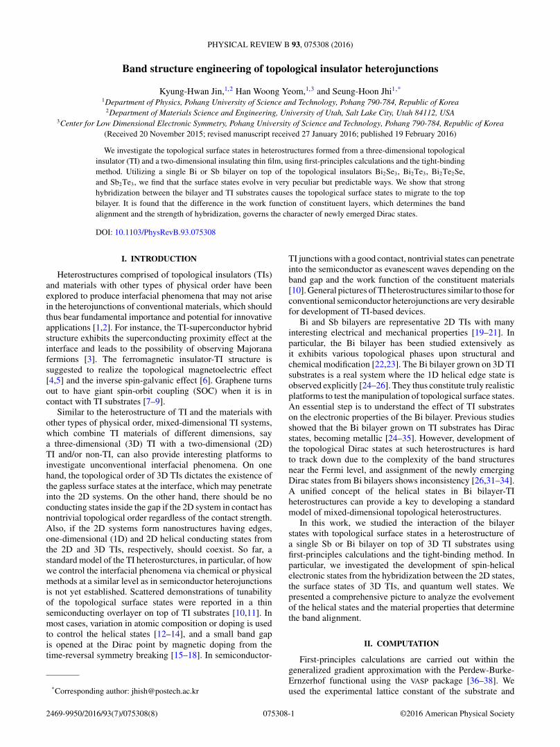
A single Sb or Bi bilayer has a buckled hexagonalstructure, and its commensurate alignment on top of the(111) surface of Bi2Se3 (BS), Bi2Te3 (BT), Bi2Te2Se (BTS),or Sb2Te3 (ST) produces a slight lattice mismatch (Ta-ble I and Fig. 1). The binding energy is given as Eb =E(bilayer + TI) − E(bilayer) − E(TI), where E(·) representsthe cohesive energies of the bilayer-6QL TI, the bilayer, and6QL TI, respectively. The Bi bilayer is weakly bound to theTI substrates with a binding energy of about ∼0.1 eV per Biatom and the equilibrium separation d � 2.9 A. Our calculatedresults are in good agreement with available experimentaldata and other calculations [27,30,33]. For the Sb bilayer,the adsorption is weaker with Eb ∼ 0.06 eV per Sb atom butits equilibrium separation is similar to that in the Bi bilayercase. The absence of direct chemical bonding indicates that thebinding is an electrostatic type. We also calculated the workfunctions of the substrates and pristine Sb and Bi bilayers[Fig. 1(d)], which determines the band alignment of the Diracstates in the heterostructures as discussed below. The Sbbilayer has a similar work function to that of TI substrateswhile the Bi bilayer has a smaller value by ∼1.5 eV.
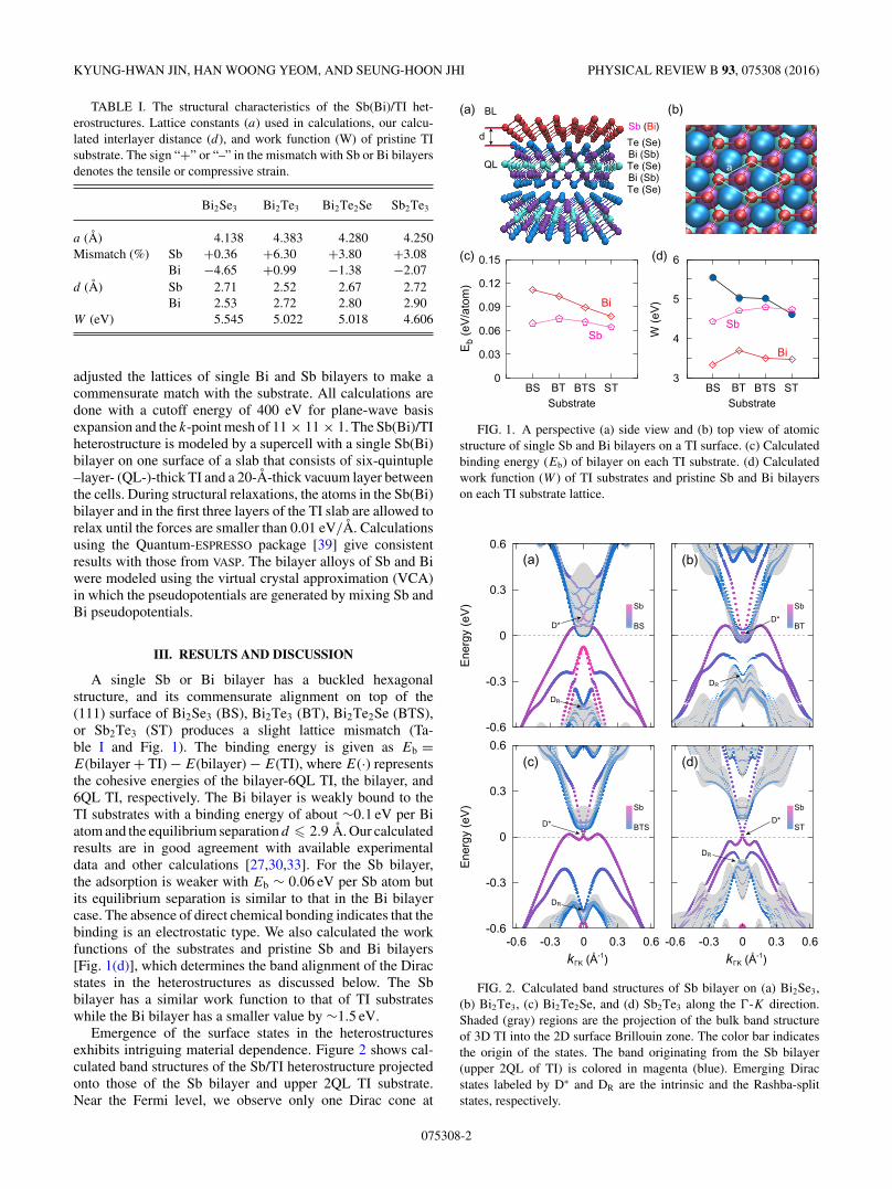
Emergence of the surface states in the heterostructuresexhibits intriguing material dependence. Figure 2 shows cal-culated band structures of the Sb/TI heterostructure projectedonto those of the Sb bilayer and upper 2QL TI substrate.Near the Fermi level, we observe only one Dirac cone at
FIG. 1. A perspective (a) side view and (b) top view of atomicstructure of single Sb and Bi bilayers on a TI surface. (c) Calculatedbinding energy (Eb) of bilayer on each TI substrate. (d) Calculatedwork function (W ) of TI substrates and pristine Sb and Bi bilayerson each TI substrate lattice.
FIG. 2. Calculated band structures of Sb bilayer on (a) Bi2Se3,(b) Bi2Te3, (c) Bi2Te2Se, and (d) Sb2Te3 along the �-K direction.Shaded (gray) regions are the projection of the bulk band structureof 3D TI into the 2D surface Brillouin zone. The color bar indicatesthe origin of the states. The band originating from the Sb bilayer(upper 2QL of TI) is colored in magenta (blue). Emerging Diracstates labeled by D∗ and DR are the intrinsic and the Rashba-splitstates, respectively.
075308-2
BAND STRUCTURE ENGINEERING OF TOPOLOGICAL . . . PHYSICAL REVIEW B 93, 075308 (2016)
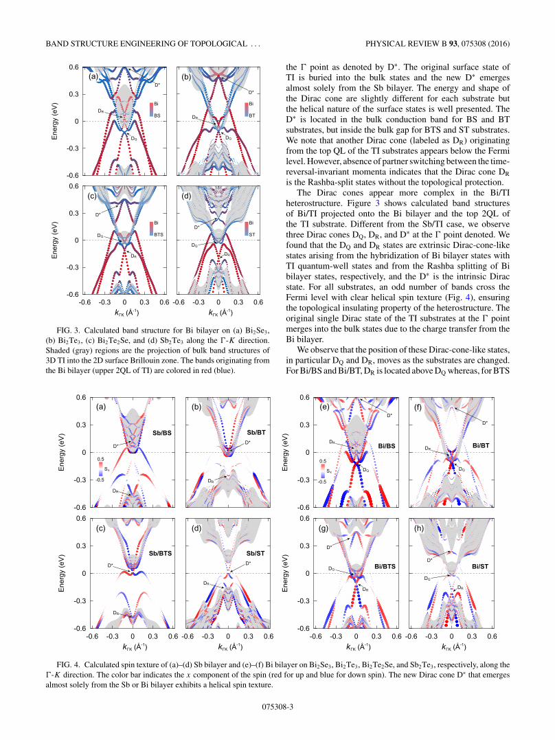
FIG. 3. Calculated band structure for Bi bilayer on (a) Bi2Se3,(b) Bi2Te3, (c) Bi2Te2Se, and (d) Sb2Te3 along the �-K direction.Shaded (gray) regions are the projection of bulk band structures of3D TI into the 2D surface Brillouin zone. The bands originating fromthe Bi bilayer (upper 2QL of TI) are colored in red (blue).
the � point as denoted by D∗. The original surface state ofTI is buried into the bulk states and the new D∗ emergesalmost solely from the Sb bilayer. The energy and shape ofthe Dirac cone are slightly different for each substrate butthe helical nature of the surface states is well presented. TheD∗ is located in the bulk conduction band for BS and BTsubstrates, but inside the bulk gap for BTS and ST substrates.We note that another Dirac cone (labeled as DR) originatingfrom the top QL of the TI substrates appears below the Fermilevel. However, absence of partner switching between the time-reversal-invariant momenta indicates that the Dirac cone DR
is the Rashba-split states without the topological protection.The Dirac cones appear more complex in the Bi/TI
heterostructure. Figure 3 shows calculated band structuresof Bi/TI projected onto the Bi bilayer and the top 2QL ofthe TI substrate. Different from the Sb/TI case, we observethree Dirac cones DQ, DR, and D∗ at the � point denoted. Wefound that the DQ and DR states are extrinsic Dirac-cone-likestates arising from the hybridization of Bi bilayer states withTI quantum-well states and from the Rashba splitting of Bibilayer states, respectively, and the D∗ is the intrinsic Diracstate. For all substrates, an odd number of bands cross theFermi level with clear helical spin texture (Fig. 4), ensuringthe topological insulating property of the heterostructure. Theoriginal single Dirac state of the TI substrates at the � pointmerges into the bulk states due to the charge transfer from theBi bilayer.
We observe that the position of these Dirac-cone-like states,in particular DQ and DR, moves as the substrates are changed.For Bi/BS and Bi/BT, DR is located above DQ whereas, for BTS
FIG. 4. Calculated spin texture of (a)–(d) Sb bilayer and (e)–(f) Bi bilayer on Bi2Se3, Bi2Te3, Bi2Te2Se, and Sb2Te3, respectively, along the�-K direction. The color bar indicates the x component of the spin (red for up and blue for down spin). The new Dirac cone D∗ that emergesalmost solely from the Sb or Bi bilayer exhibits a helical spin texture.
075308-3
KYUNG-HWAN JIN, HAN WOONG YEOM, AND SEUNG-HOON JHI PHYSICAL REVIEW B 93, 075308 (2016)
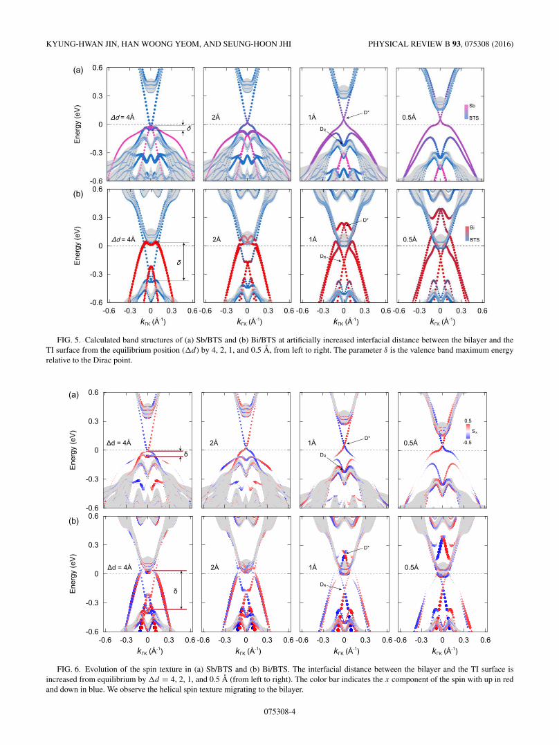
FIG. 5. Calculated band structures of (a) Sb/BTS and (b) Bi/BTS at artificially increased interfacial distance between the bilayer and theTI surface from the equilibrium position (�d) by 4, 2, 1, and 0.5 A, from left to right. The parameter δ is the valence band maximum energyrelative to the Dirac point.
FIG. 6. Evolution of the spin texture in (a) Sb/BTS and (b) Bi/BTS. The interfacial distance between the bilayer and the TI surface isincreased from equilibrium by �d = 4, 2, 1, and 0.5 A (from left to right). The color bar indicates the x component of the spin with up in redand down in blue. We observe the helical spin texture migrating to the bilayer.
075308-4
BAND STRUCTURE ENGINEERING OF TOPOLOGICAL . . . PHYSICAL REVIEW B 93, 075308 (2016)
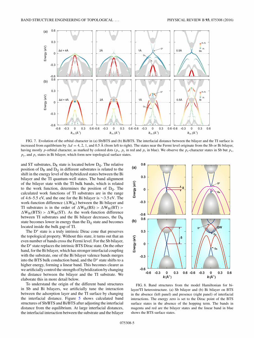
FIG. 7. Evolution of the orbital character in (a) Sb/BTS and (b) Bi/BTS. The interfacial distance between the bilayer and the TI surface isincreased from equilibrium by �d = 4, 2, 1, and 0.5 A (from left to right). The states near the Fermi level originate from the Sb or Bi bilayer,having mostly p-orbital character, as marked by colored dots (px, py in red and pz in blue). We observe the pz-character states in Sb but px,py, and pz states in Bi bilayer, which form new topological surface states.
and ST substrates, DR state is located below DQ. The relativeposition of DR and DQ in different substrates is related to theshift in the energy level of the hybridized states between the Bibilayer and the TI quantum-well states. The band alignmentof the bilayer state with the TI bulk bands, which is relatedto the work function, determines the position of DQ. Thecalculated work functions of TI substrates are in the rangeof 4.6–5.5 eV, and the one for the Bi bilayer is ∼3.5 eV. Thework-function difference (�WBi) between the Bi bilayer andTI substrates is in the order of �WBi(BS) > �WBi(BT) >
�WBi(BTS) > �WBi(ST). As the work-function differencebetween TI substrates and the Bi bilayer decreases, the DR
state becomes lower in energy than the DQ state and becomeslocated inside the bulk gap of TI.
The D∗ state is a truly intrinsic Dirac cone that preservesthe topological property. Without this state, it turns out that aneven number of bands cross the Fermi level. For the Sb bilayer,the D∗ state replaces the intrinsic BTS Dirac state. On the otherhand, for the Bi bilayer, which has stronger interfacial couplingwith the substrate, one of the Bi bilayer valence bands mergesinto the BTS bulk conduction band, and the D∗ state shifts to ahigher energy, forming a linear band. This becomes clearer aswe artificially control the strength of hybridization by changingthe distance between the bilayer and the TI substrate. Weelaborate this in more detail below.
To understand the origin of the different band structuresin Sb and Bi bilayers, we artificially tune the interactionbetween the adsorption layer and the TI surface by changingthe interfacial distance. Figure 5 shows calculated bandstructures of Sb/BTS and Bi/BTS after adjusting the interfacialdistance from the equilibrium. At large interfacial distances,the interfacial interaction between the substrate and the bilayer
FIG. 8. Band structures from the model Hamiltonian for bi-layer/TI heterostructure. (a) Sb bilayer and (b) Bi bilayer on BTSin the absence (left panel) and presence (right panel) of interfacialinteractions. The energy zero is set to the Dirac point of the BTSsurface states in the absence of the hopping term. The bands inmagenta and red are the bilayer states and the linear band in blueshows the BTS surface states.
075308-5
KYUNG-HWAN JIN, HAN WOONG YEOM, AND SEUNG-HOON JHI PHYSICAL REVIEW B 93, 075308 (2016)
FIG. 9. Calculated band structures of BTS1QL/BTS5QL with the interfacial distance increased by �d = 4, 1, 0.5, and 0 A (from left to right)from the equilibrium distance.
is negligible and the band structure is a simple superposition ofthe bands of the isolated Sb/Bi bilayer and the BTS substrate.We note that the valence band maximum (VBM) relative tothe Dirac point is about ∼0.05 eV for Sb and ∼0.4 eV for Bidue to the work-function difference. The Sb bilayer has a workfunction of about ∼5 eV, similar to that of BTS, and its VBMis well aligned with that of BTS. However, the Bi bilayer withthe work function of ∼3.5 eV has the VBM in the BTS bulkconduction band. This explains the different band shapes forSb and Bi bilayers. As the interfacial distance is decreased, weobserve a slight band splitting in doubly degenerate bands ofthe bilayer due to the broken inversion symmetry. When theinterfacial coupling is enhanced, the bands split further andstart to hybridize with the TI bands, eventually forming newDirac cones. This behavior is also found in the evolution of thespin texture and orbital character as the interfacial distance ischanged (Figs. 6 and 7).
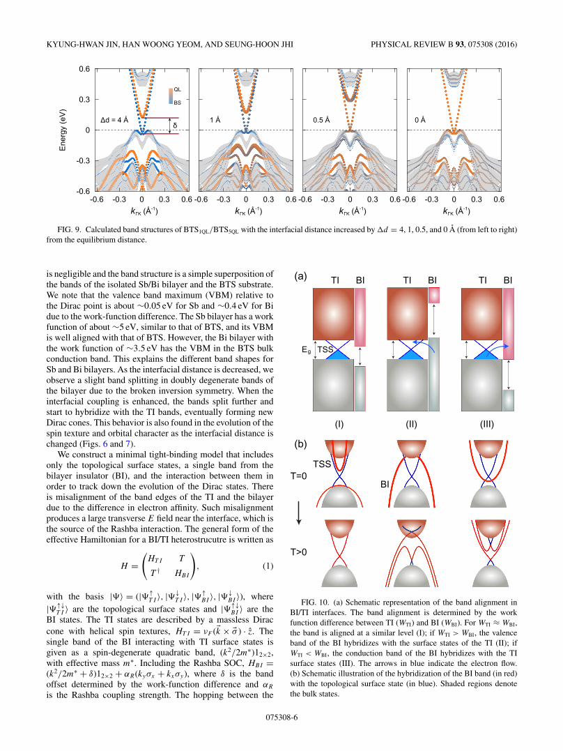
We construct a minimal tight-binding model that includesonly the topological surface states, a single band from thebilayer insulator (BI), and the interaction between them inorder to track down the evolution of the Dirac states. Thereis misalignment of the band edges of the TI and the bilayerdue to the difference in electron affinity. Such misalignmentproduces a large transverse E field near the interface, which isthe source of the Rashba interaction. The general form of theeffective Hamiltonian for a BI/TI heterostrucutre is written as
H =(
HT I T
T † HBI
), (1)
with the basis |�〉 = (|�↑T I 〉, |�↓
T I 〉, |�↑BI 〉, |�↓
BI 〉), where|�↑↓
T I 〉 are the topological surface states and |�↑↓BI 〉 are the
BI states. The TI states are described by a massless Diraccone with helical spin textures, HT I = νF (�k × �σ ) · z. Thesingle band of the BI interacting with TI surface states isgiven as a spin-degenerate quadratic band, (k2/2m∗)12×2,with effective mass m∗. Including the Rashba SOC, HBI =(k2/2m∗ + δ)12×2 + αR(kyσx + kxσy), where δ is the bandoffset determined by the work-function difference and αR
is the Rashba coupling strength. The hopping between the
FIG. 10. (a) Schematic representation of the band alignment inBI/TI interfaces. The band alignment is determined by the workfunction difference between TI (WTI) and BI (WBI). For WTI ≈ WBI,the band is aligned at a similar level (I); if WTI > WBI, the valenceband of the BI hybridizes with the surface states of the TI (II); ifWTI < WBI, the conduction band of the BI hybridizes with the TIsurface states (III). The arrows in blue indicate the electron flow.(b) Schematic illustration of the hybridization of the BI band (in red)with the topological surface state (in blue). Shaded regions denotethe bulk states.
075308-6
BAND STRUCTURE ENGINEERING OF TOPOLOGICAL . . . PHYSICAL REVIEW B 93, 075308 (2016)
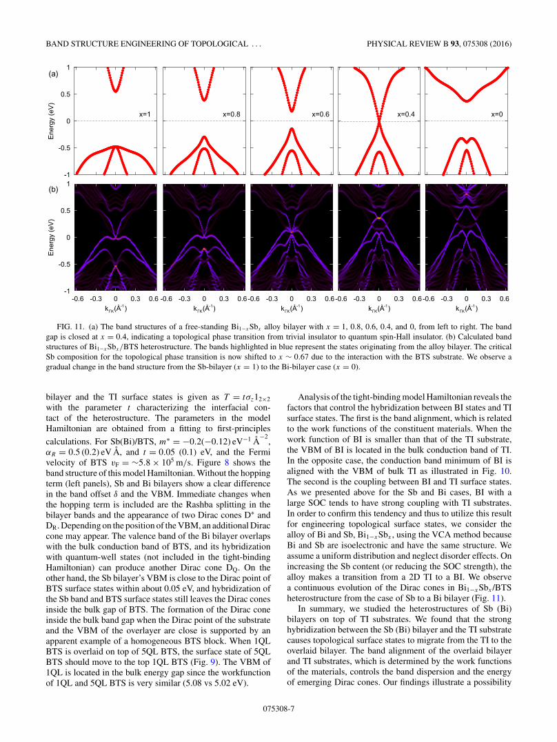
FIG. 11. (a) The band structures of a free-standing Bi1−xSbx alloy bilayer with x = 1, 0.8, 0.6, 0.4, and 0, from left to right. The bandgap is closed at x = 0.4, indicating a topological phase transition from trivial insulator to quantum spin-Hall insulator. (b) Calculated bandstructures of Bi1−xSbx/BTS heterostructure. The bands highlighted in blue represent the states originating from the alloy bilayer. The criticalSb composition for the topological phase transition is now shifted to x ∼ 0.67 due to the interaction with the BTS substrate. We observe agradual change in the band structure from the Sb-bilayer (x = 1) to the Bi-bilayer case (x = 0).
bilayer and the TI surface states is given as T = tσz12×2
with the parameter t characterizing the interfacial con-tact of the heterostructure. The parameters in the modelHamiltonian are obtained from a fitting to first-principles
calculations. For Sb(Bi)/BTS, m∗ = −0.2(−0.12) eV−1 A−2
,αR = 0.5 (0.2) eV A, and t = 0.05 (0.1) eV, and the Fermivelocity of BTS vF = ∼5.8 × 10⁵ m/s. Figure 8 shows theband structure of this model Hamiltonian. Without the hoppingterm (left panels), Sb and Bi bilayers show a clear differencein the band offset δ and the VBM. Immediate changes whenthe hopping term is included are the Rashba splitting in thebilayer bands and the appearance of two Dirac cones D∗ andDR. Depending on the position of the VBM, an additional Diraccone may appear. The valence band of the Bi bilayer overlapswith the bulk conduction band of BTS, and its hybridizationwith quantum-well states (not included in the tight-bindingHamiltonian) can produce another Dirac cone DQ. On theother hand, the Sb bilayer’s VBM is close to the Dirac point ofBTS surface states within about 0.05 eV, and hybridization ofthe Sb band and BTS surface states still leaves the Dirac conesinside the bulk gap of BTS. The formation of the Dirac coneinside the bulk band gap when the Dirac point of the substrateand the VBM of the overlayer are close is supported by anapparent example of a homogeneous BTS block. When 1QLBTS is overlaid on top of 5QL BTS, the surface state of 5QLBTS should move to the top 1QL BTS (Fig. 9). The VBM of1QL is located in the bulk energy gap since the workfunctionof 1QL and 5QL BTS is very similar (5.08 vs 5.02 eV).
Analysis of the tight-binding model Hamiltonian reveals thefactors that control the hybridization between BI states and TIsurface states. The first is the band alignment, which is relatedto the work functions of the constituent materials. When thework function of BI is smaller than that of the TI substrate,the VBM of BI is located in the bulk conduction band of TI.In the opposite case, the conduction band minimum of BI isaligned with the VBM of bulk TI as illustrated in Fig. 10.The second is the coupling between BI and TI surface states.As we presented above for the Sb and Bi cases, BI with alarge SOC tends to have strong coupling with TI substrates.In order to confirm this tendency and thus to utilize this resultfor engineering topological surface states, we consider thealloy of Bi and Sb, Bi1−xSbx , using the VCA method becauseBi and Sb are isoelectronic and have the same structure. Weassume a uniform distribution and neglect disorder effects. Onincreasing the Sb content (or reducing the SOC strength), thealloy makes a transition from a 2D TI to a BI. We observea continuous evolution of the Dirac cones in Bi1−xSbx /BTSheterostructure from the case of Sb to a Bi bilayer (Fig. 11).
In summary, we studied the heterostructures of Sb (Bi)bilayers on top of TI substrates. We found that the stronghybridization between the Sb (Bi) bilayer and the TI substratecauses topological surface states to migrate from the TI to theoverlaid bilayer. The band alignment of the overlaid bilayerand TI substrates, which is determined by the work functionsof the materials, controls the band dispersion and the energyof emerging Dirac cones. Our findings illustrate a possibility
075308-7
KYUNG-HWAN JIN, HAN WOONG YEOM, AND SEUNG-HOON JHI PHYSICAL REVIEW B 93, 075308 (2016)
of controlling the surface states and topological phases inthe heterostructures and open a way of designing appropriatematerial combinations for device applications. Also our studyhelps understand the complex evolution of the surface statesand the topological properties in TI heterostructures.
ACKNOWLEDGMENTS
This work was supported by the National Research Foun-dation of Korea through the SRC program (Grant No. 2011-0030046) and the Institute for Basic Science (IBS) (Grant No.IBS-R014-D1).
[1] M. Z. Hasan and C. L. Kane, Rev. Mod. Phys. 82, 3045(2010).
[2] X.-L. Qi and S.-C. Zhang, Rev. Mod. Phys. 83, 1057 (2011).[3] L. Fu and C. L. Kane, Phys. Rev. Lett. 100, 096407 (2008).[4] X.-L. Qi, T. L. Hughes, and S.-C. Zhang, Phys. Rev. B 78,
195424 (2008).[5] X.-L. Qi, R. Li, J. Zang, and S.-C. Zhang, Science 323, 1184
(2009).[6] I. Garate and M. Franz, Phys. Rev. Lett. 104, 146802 (2010).[7] K.-H. Jin and S.-H. Jhi, Phys. Rev. B 87, 075442 (2013).[8] J. Zhang, C. Triola, and E. Rossi, Phys. Rev. Lett. 112, 096802
(2014).[9] P. Lee, J.-H. Jin, S. J. Sung, J. G. Kim, M.-T. Ryu, H.-M. Park,
S.-H. Jhi, N. Kim, Y. Kim, S. U. Yu, K. S. Kim, D. Y. Noh, andJ. Chung, ACS Nano 9, 10861 (2015).
[10] G. Wu, H. Chen, Y. Sun, X. Li, P. Cui, C. Franchini, J. Wang,X.-Q. Chen, and Z. Zhang, Sci. Rep. 3, 1233 (2013).
[11] T. V. Menshchikova, M. M. Otrokov, S. S. Tsirkin, D. A.Samorokov, V. V. Bebneva, A. Ernst, V. M. Kuznetsov, andE. V. Chulkov, Nano Lett. 13, 6064 (2013).
[12] Y. L. Chen, J. G. Analytis, J.-H. Chu, Z. K. Liu, S.-K. Mo,X. L. Qi, H. J. Zhang, D. H. Lu, X. Dai, Z. Fang, S. C. Zhang, I.R. Fisher, Z. Hussain, and Z.-X. Shen, Science 325, 178 (2009).
[13] J. Zhang, C.-Z. Chang, Z. Zhang, J. Wen, X. Feng, K. Li, M.Liu, K. He, L. Wang, X. Chen, Q.-K. Xue, X. Ma, and Y. Wang,Nat. Commun. 2, 574 (2011).
[14] T. Arakane, T. Sato, S. Souma, K. Kosaka, K. Nakayama, M.Komatsu, T. Takahashi, Z. Ren, K. Segawa, and Y. Ando, Nat.Commun. 3, 636 (2012).
[15] Y. L. Chen, J.-H. Chu, J. G. Analytis, Z. K. Liu, K. Igarashi,H.-H. Kuo, X. L. Qi, S. K. Mo, R. G. Moore, D. H. Lu, M.Hashimoto, T. Sasagawa, S. C. Zhang, I. R. Fisher, Z. Hussain,and Z. X. Shen, Science 329, 659 (2010).
[16] L. A. Wray, S.-Y. Xu, Y. Xia, D. Hsieh, A. V. Fedorov, Y. S.Hor, R. J. Cava, A. Bansil, H. Lin, and M. Z. Hasan, Nat. Phys.7, 32 (2011).
[17] J. Henk, M. Flieger, I. V. Maznichenko, I. Mertig, A. Ernst,S. V. Eremeev, and E. V. Chulkov, Phys. Rev. Lett. 109, 076801(2012).
[18] K.-H. Jin and S.-H. Jhi, J. Phys.: Condens. Matter 24, 175001(2012).
[19] S. Murakami, Phys. Rev. Lett. 97, 236805 (2006).[20] M. Wada, S. Murakami, F. Freimuth, and G. Bihlmayer, Phys.
Rev. B 83, 121310 (2011).
[21] F.-C. Chuang, C.-H. Hsu, C.-Y. Chen, Z.-Q. Huang, V. Ozolins,H. Lin, and A. Bansil, Appl. Phys. Lett. 102, 022424 (2013).
[22] Z. Song, C.-C. Liu, J. Yang, J. Han, M. Ye, B. Fu, Y. Yang, Q.Niu, J. Lu, and Y. Yao, NPG Asia Mater. 6, e147 (2014).
[23] K.-H. Jin and S.-H. Jhi, Sci. Rep. 5, 8426 (2015).[24] T. Hirahara, G. Bihlmayer, Y. Sakamoto, M. Yamada, H.
Miyazaki, S.-I. Kimura, S. Blugel, and S. Hasegawa, Phys. Rev.Lett. 107, 166801 (2011).
[25] F. Yang, L. Miao, Z. F. Wang, M.-Y. Yao, F. Zhu, Y. R. Song,M.-X. Wang, J.-P. Xu, A. V. Fedorov, Z. Sun, G. B. Zhang, C.Liu, F. Liu, D. Qian, C. L. Gao, and J.-F. Jia, Phys. Rev. Lett.109, 016801 (2012).
[26] S. H. Kim, K.-H. Jin, J. Park, J. S. Kim, S.-H. Jhi, T.-H. Kim,and H. W. Yeom, Phys. Rev. B 89, 155436 (2014).
[27] N. Fukui, T. Hirahara, T. Shirasawa, T. Takahashi, K. Kobayashi,and S. Hasegawa, Phys. Rev. B 85, 115426 (2012).
[28] Z. F. Wang, M.-Y. Yao, W. Ming, L. Miao, F. Zhu, C. Liu, C.L. Gao, D. Qian, J.-F. Jia, and F. Liu, Nat. Commun. 4, 1384(2013).
[29] L. Miao, Z. F. Wang, W. Ming, M.-Y. Yao, M. Wang, F. Yang,Y. R. Song, F. Zhu, A. V. Fedorov, Z. Sun, C. L. Gao, C. Liu,Q.-K. Xue, C.-X. Liu, F. Liu, D. Qian, and J.-F. Jia, Proc. Natl.Acad. Sci. USA 110, 2758 (2013).
[30] G. Q. Huang and B. Li, EPL 104, 57003 (2013).[31] L. Miao, Z. F. Wang, M.-Y. Yao, F. Zhu, J. H. Dil, C. L. Gao,
Canhua Liu, F. Liu, D. Qian, and J.-F. Jia, Phys. Rev. B 89,155116 (2014).
[32] A. Eich, M. Michiardi, G. Bihlmayer, X.-G. Zhu, J.-L. Mi, Bo B.Iversen, R. Wiesendanger, Ph. Hofmann, A. A. Khajetoorians,and J. Wiebe, Phys. Rev. B 90, 155414 (2014).
[33] K. Govaerts, K. Park, C. De Beule, B. Partoens, and D. Lamoen,Phys. Rev. B 90, 155124 (2014).
[34] H. W. Yeom, S. H. Kim, W. J. Shin, K.-H. Jin, J. Park, T.-H.Kim, J. S. Kim, H. Ishikawa, K. Sakamoto, and S.-H. Jhi, Phys.Rev. B 90, 235401 (2014).
[35] T. Shoman, A. Takayama, T. Sato, S. Souma, T. Takahashi, T.Oguchi, K. Segawa, and Y. Ando, Nat. Commun. 6, 6547 (2015).
[36] P. E. Blochl, Phys. Rev. B 50, 17953 (1994).[37] J. P. Perdew, K. Burke, and M. Ernzerhof, Phys. Rev. Lett. 77,
3865 (1996).[38] G. Kresse and D. Joubert, Phys. Rev. B 59, 1758 (1999).[39] P. Giannozzi, S. Baroni, N. Bonini, M. Calandra, R. Car, C.
Cavazzoni, D. Ceresoli, G. L. Chiarotti, M. Cococcioni, and I.Dabo, J. Phys.: Condens. Matter 21, 395502 (2009).
075308-8


