Embed Size (px)
Citation preview
1
Quasiparticle scattering from topological crystalline insulator SnTe (001)
surface states
Duming Zhang,1,2 Hongwoo Baek,1,3 Jeonghoon Ha,1,2 Tong Zhang,1,2,* Jonathan E. Wyrick,1
Albert V. Davydov,4 Young Kuk,3 and Joseph A. Stroscio1,†
1Center for Nanoscale Science and Technology, National Institute of Standards and Technology,
Gaithersburg, MD 20899, USA 2Maryland NanoCenter, University of Maryland, College Park, MD 20742, USA
3Department of Physics and Astronomy, Seoul National University, Seoul, 151-747, Korea 4Material Measurement Laboratory, National Institute of Standards and Technology,
Gaithersburg, MD 20899, USA
Recently, the topological classification of electronic states has been extended to a new class
of matter known as topological crystalline insulators. Similar to topological insulators, topological
crystalline insulators also have spin-momentum locked surface states; but they only exist on
specific crystal planes that are protected by crystal reflection symmetry. Here, we report an ultra-
low temperature scanning tunneling microscopy and spectroscopy study on topological crystalline
insulator SnTe nanoplates grown by molecular beam epitaxy. We observed quasiparticle
interference patterns on the SnTe (001) surface that can be interpreted in terms of electron
scattering from the four Fermi pockets of the topological crystalline insulator surface states in the
first surface Brillouin zone. A quantitative analysis of the energy dispersion of the quasiparticle
interference intensity shows two high energy features related to the crossing point beyond the
Lifshitz transition when the two neighboring low energy surface bands near the point merge.
A comparison between the experimental and computed quasiparticle interference patterns reveals
possible spin texture of the surface states.
* Current address: Department of Physics, Fudan University, Shanghai 200433, China. † To whom correspondence should be addressed: [email protected]
2
I. Introduction
Topological insulators are a new classification of matter characterized by a bulk insulating
gap and gapless surface states protected by time reversal symmetry.1–3 This is realized by spin-
orbit coupling induced band inversion with an odd number of Dirac cones. Recently, the
topological classification of materials has been extended to a new phase of matter, topological
crystalline insulators.4,5 In contrast to topological insulators, topological crystalline insulators arise
from crystal reflection symmetry and are characterized by topological surface states with an even
number of Dirac cones. The first topological crystalline insulator was predicted in the SnTe class
of materials,5 the surface states of which were soon observed in Pb1-xSnxSe,6 SnTe,7 and Pb1-
xSnxTe8,9 bulk crystals by angle-resolved photoemission spectroscopy (ARPES). The surface states
of this class of topological crystalline insulators have also been further studied by scanning
tunneling microscopy (STM)10–12 as well as electrical transport.13,14 Most of the studies so far have
focused on cleaved bulk samples. However, there are several advantages to grow these topological
materials in the form of nanostructures and thin films. First, by going to lower dimensions, the
surface contribution can potentially be enhanced with increased surface-to-volume ratio.14,15
Furthermore, compared to bulk crystals, it is much easier to fabricate devices made from
nanostructures and to interface them with other materials such as superconductors16,17 and
magnetic materials.18 Motivated by these advantages, we performed an STM study of the
topological surface states of SnTe nanoplates.
Here, we report synthesis and in-situ STM measurements on single crystalline SnTe
nanoplates synthesized by molecular beam epitaxy (MBE). We carried out Fourier transform
scanning tunneling spectroscopy (FT-STS) using an ultra-low temperature STM on the SnTe (001)
surface. We observed quasiparticle interference patterns in the differential tunneling conductance,
3
dI/dV, maps, which can be interpreted in terms of scattering among the four Fermi pockets of the
topological surfaces states in the first surface Brillouin zone of (001) planes. A quantitative
analysis of the energy dispersion of the quasiparticle interference intensity reveals features
associated with the high energy crossing point in the surface bands.
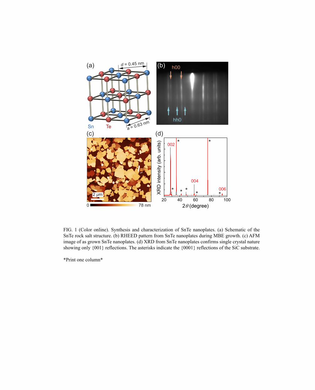
II. Synthesis and Characterization of SnTe Nanoplates
The SnTe nanoplates studied in this work were synthesized by MBE using a high purity
SnTe compound source (pieces, 99.999%) and a separate elemental Sn source (shots, 99.999%).
After a 30-minute anneal of a graphitized 6H-SiC (0001) substrate at 300 °C, SnTe was deposited
onto the substrate at ≈ 230 °C with a typical growth rate between 0.3 nm/min and 0.7 nm/min and
a Sn to SnTe flux ratio in the range of 0 % to 15 %. We note that the compensation of extra Sn
flux (up to 15 % in flux ratio) did not seem to reduce the overall p-doping concentration in the
samples. SnTe has a cubic rock salt crystal structure with a lattice constant a = 0.633 nm. A
schematic of the SnTe (001) surface is illustrated in Fig. 1(a). Reflection high energy electron
diffraction (RHEED) was used to monitor the growth front, which indicates single crystal growth
mode [Fig. 1(b)]. Ex-situ atomic force microscopy (AFM) [Fig. 1(c)] shows that all these
nanoplates are roughly square shaped, suggesting they have a preferential out-of-plane orientation
along the <001> direction. This preferential orientation of the nanoplates is confirmed by X-ray
diffraction (XRD) measurement, showing only the {001} reflections [Fig. 1(d)]. Electron
backscatter diffraction measurements on individual nanoplates also confirmed the nanoplates were
single crystalline with (001) oriented top surfaces.
4
III. Experimental Results
A. Sn vacancy defects
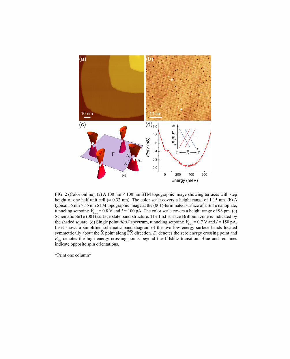
After the growth of SnTe nanoplates, the sample was immediately transferred from the
MBE chamber to an interconnected 10 mK ultra-low temperature STM without breaking
vacuum.19 The STM topographic image in Fig. 2(a) reveals the SnTe (001) surface with large
atomically flat terraces separated by a step height of one half unit cell (≈ 0.32 nm, see Fig. 1(a)).
Fig. 2(b) shows a smaller scale STM topographic image of the SnTe (001) surface, with a number
of defects, which is a characteristic of these samples. At positive sample bias (Vbias = 0.8 V), only
the Sn sublattice is mainly revealed as electrons tunnel into the empty states of the sample. The
lattice spacing is consistent with (110) interplanar distance / 2 0.45d a nm as illustrated in
Fig. 1(a). Apart from some adatoms at the surface, many vacancies, presumably Sn vacancies, are
clearly visible. This is consistent with as-grown SnTe bulk crystals, which are typically p-doped
due to Sn vacancies.7 The long wavelength roughness at the SnTe surface (root mean square
roughness = 8.8 pm) may be due to the underlying structure of multi-layer graphene grown on the
SiC substrate, which was used as a substrate for the SnTe growth.
The (001) surface of SnTe has been predicted5 and shown7 to have topological surface
states, a schematic of which is shown in Fig. 2(c). By rotation symmetry, there are four low energy
bands near the four equivalent points in the first surface Brillouin zone indicated by the shaded
square. Due to crystal reflection symmetry, there are two low energy surface bands located
symmetrically about the point along the direction. The positions of the neighboring zero
energy crossing points are denoted as 1 and
2 . When the energy is increased/decreased from
the zero energy crossing point, the two low energy surface bands on both sides of the point
5
touch each other, exhibiting a Lifshitz transition, where two electron/hole pockets reconnect to
form a large electron/hole and a small hole/electron pocket centered at the point. When the
energy is further increased/decreased from the zero energy crossing point, the high energy surface
bands start from the high energy crossing points at the point.
The local density of states of the SnTe nanoplates was obtained by measuring the bias
dependent dI/dV spectra with a lock-in amplifier. Fig. 2(d) is a typical single point spectrum with
a minimum at ≈ 350 meV. The inset shows a simplified schematic of the two low energy surface
bands located symmetrically about the point along the direction. Comparing with this
surface state band diagram, we assign this dI/dV minimum as the zero energy crossing point, E0.
The position of the zero energy crossing point indicates that our nanoplates are p-doped, consistent
with the observation of large amount of Sn vacancies at the surface. Similar to the STM work on
cleaved bulk Pb1-xSnxSe,10 we did not observe strong features in the spectra associated with the
Lifshitz transition. However, features related to the Lifshitz transition were recently observed in
Ref. [11] in Pb1-xSnxSe, and it is uncertain why they are not visible in our spectra on SnTe.
Evidence for the Lifshitz transition is seen in our data in the analysis of the quasiparticle
interference presented in section III, below. Based on the position of the zero energy crossing point
and the band gap (≈ 0.18 eV) of bulk SnTe, the kink near the zero bias in the spectrum is possibly
related to states in the bulk valence band.
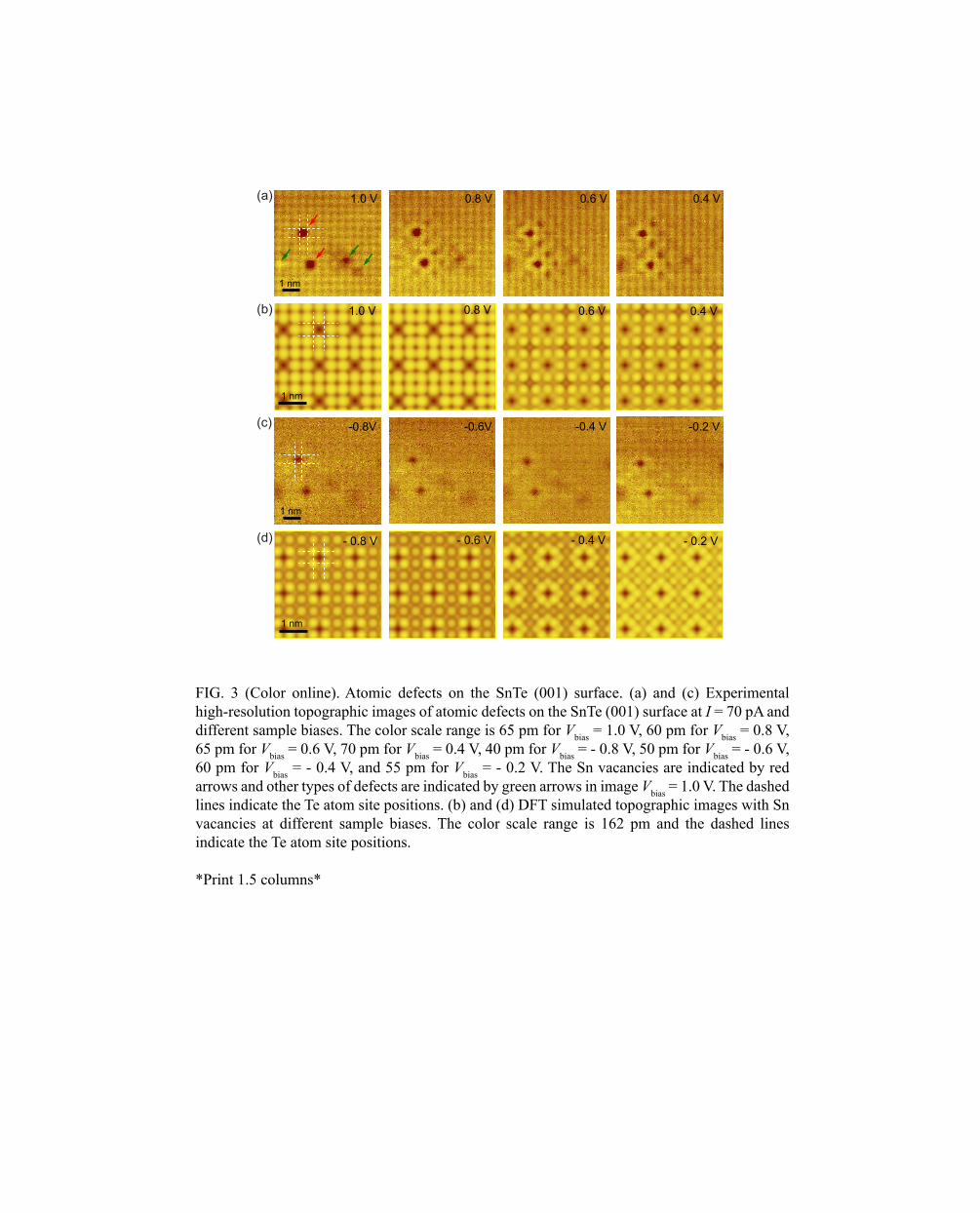
The p-doping is generally attributed to the tendency to grow nonstoichiometric SnTe with
Sn vacancies, which can be observed in the STM images. Figures 3(a) and 3(c) show a series of
high-resolution topographic images of atomic defects from the same area at different sample
biases. At high positive sample biases [Fig. 3(a)], electrons tunnel from the tip into the empty states
of the conduction band and image mainly the Sn sublattice. The absent rows of Te atoms are
6
between the Sn rows as indicated by the white dashed lines in Fig. 3(a). We can clearly see two
missing Sn atoms at the surface indicated by the red arrows, which we identify as Sn vacancies at
the surface layer. This can be further confirmed by imaging the same area at negative sample biases
[Fig. 3(c)]. At a negative bias, electrons tunnel from the filled states of the valence band into the
tip and the Te sublattice is enhanced in the topographic images. By comparing the position of the
two sublattices, we can identify that the Sn vacancies at the top surface layer are located at the
center of four neighboring Te atoms [Fig. 3(c)]. The Te atom rows are indicated by the white
dashed lines in Fig. 3(c). We note that the Sn sublattice in the image has already switched to the
Te sublattice with the Sn vacancy sites at the center of four neighboring Te atoms for energies near
the zero energy crossing point. This is likely due to hybridization effects induced by the large spin-
orbit coupling across the bulk band gap.
To further verify the Sn vacancies observed at the SnTe (001) surface, we simulated the
STM images in Figs. 3(b) and 3(d) as integrated charge density iso-surfaces from density function
theory (DFT) calculations using the generalized gradient approximation for the exchange-
correlation functional.20–24 The atomic configuration consisted of a 3 layer slab with 3×3 surface
unit cells having one surface Sn atom removed while all other atoms were fixed at their bulk
positions. A real space grid spacing of 30 pm and a k-point mesh of 5×5×1 were used with a super-
cell that included 1 nm of vacuum along the direction normal to the surface. For comparison to the
experimentally measured STM images, each simulated image has its super-cell repeated 3 times
in each direction (for a total of 9×9 unit cells with 9 vacancies per image). As we can see in Figs.
3(b) and 3(d), the simulated STM images correctly capture the main features of the experimental
data: vacancies at Sn atomic sites at positive sample biases occur in line with the Sn rows and in
between the Te atomic sites at negative sample biases. There are also several other types of defects
7
indicated by the green arrows in Fig. 3(a), which could be anti-sites or vacancies underneath the
surface layer. Identification of these different types of defects would require further DFT
simulations.
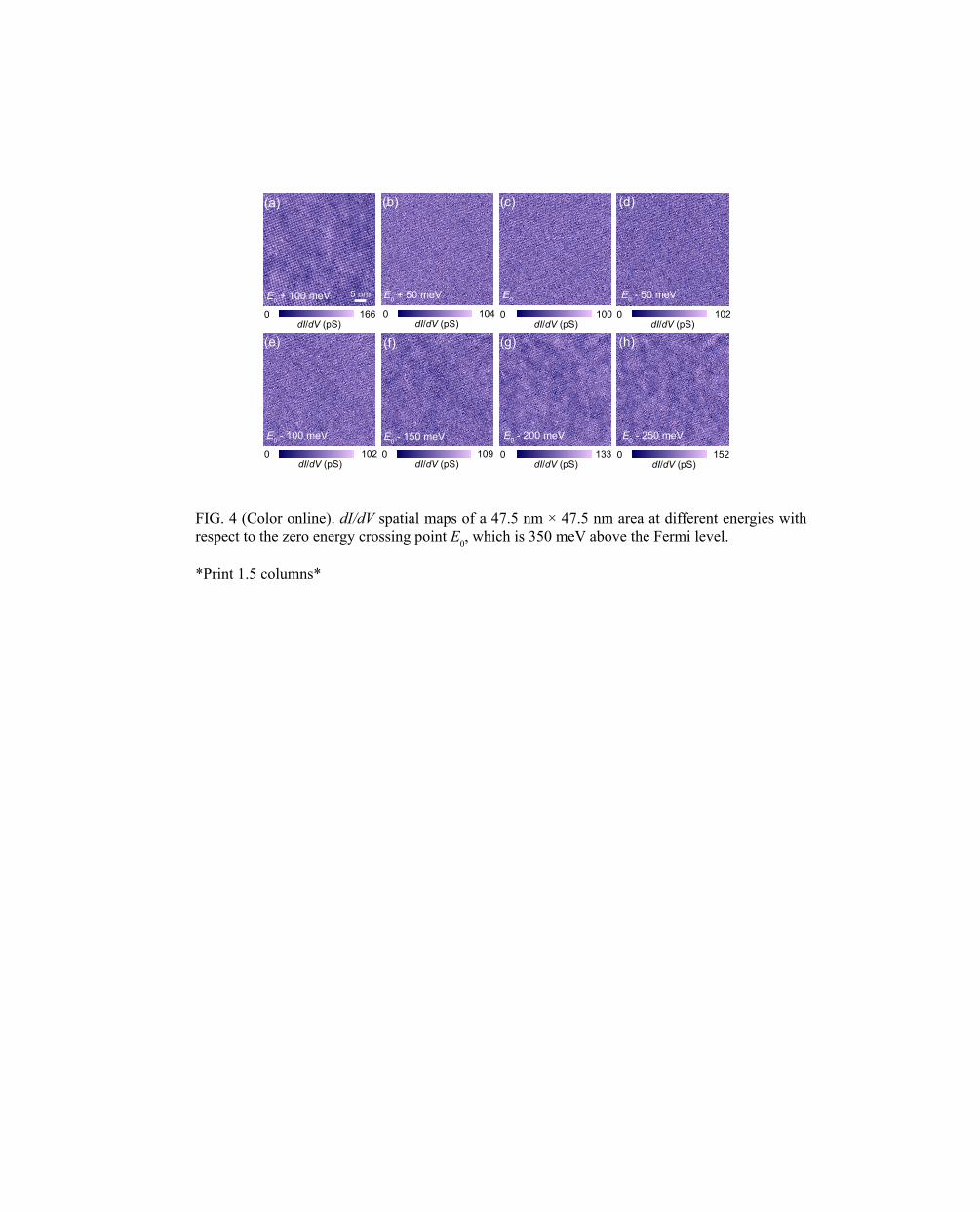
B. Quasiparticle interference
The presence of these surface defects is actually useful for studying the Fermi surface of
SnTe through electron scattering. Indeed, clues of such scattering from defects can already be seen
in topographic images as interference patterns around the Sn vacancies [Fig. 3(a)]. To better
understand the scattering process, we study quasiparticle interference patterns obtained from FT-
STS maps, which can provide the real space and momentum space electronic structure information
simultaneously. This method has been applied to study noble metal surface states,25 high-Tc
superconductors,26 graphene27,28 as well as topological materials.29 Figure 4 shows interference
patterns in STS (dI/dV) maps at different sample biases with respect to the zero energy crossing
point E0 of 350 meV. The image size (47.5 nm × 47.5 nm) and resolution (475 pixels × 475 pixels)
were chosen to cover at least the first two Brillouin zones with a resolution better than 1 % of the
Brillouin zone size. By taking the Fourier transform of the STS maps, we can measure the
quasiparticle scattering vectors as a difference of the initial and final wave vectors, q = kf - ki, for
elastic scattering. Combined with information on the surface band structure in k space, we can
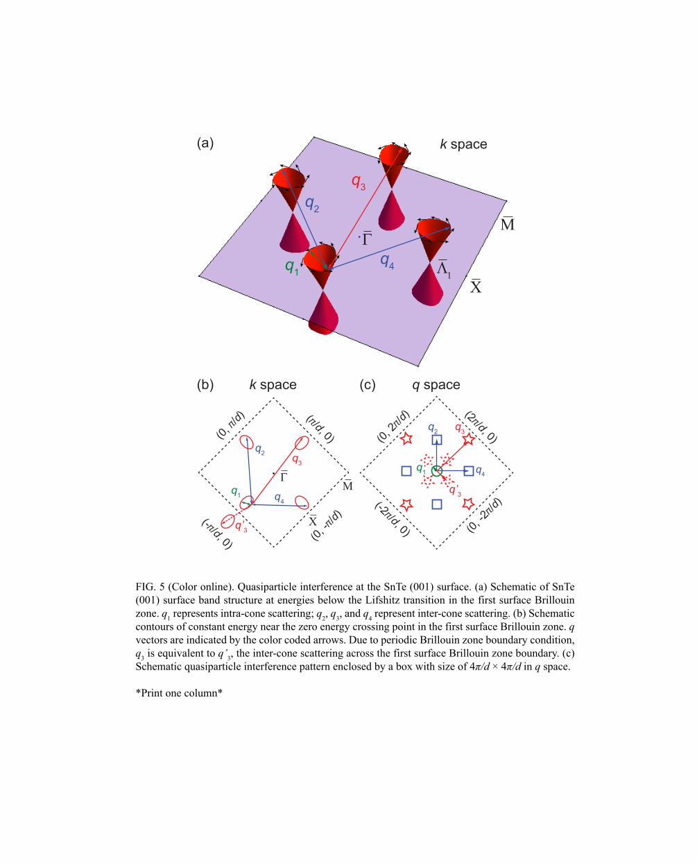
study the Fermi surface and possible spin textures of the surface states. Figure 5(a) shows a 3D
illustration of the low energy surface bands below the Lifshitz transition in the first surface
Brillouin zone. Theoretically expected spin texture of the topological crystalline insulator surface
states is indicated by the small arrows. Possible elastic scattering between kj(E) is indicated by the
color coded arrows: 1q represents intra-cone scattering and 2q – 4q represent inter-cone scattering.
In Fig. 5(b), we show the schematic contours of constant energy of the surface states near the zero
8
energy crossing point enclosed in the first surface Brillouin zone with size of 2π/d × 2π/d. We also
include 3'q which represents the inter-cone scattering between the two neighboring low energy
bands located symmetrically about the point. Due to the periodic Brillouin zone boundary
condition, 3'q is equivalent to
3q . The quasiparticle interference patterns from the first surface
Brillouin zone can be described in terms of the q wave vectors within a box with size of 4π/d ×
4π/d [Fig. 5(c)]. The intra-cone scattering (1q ) is represented by the circle symbol at the center of
the box and the inter-cone scattering ( 2q – 4q ) is represented by the square and star symbols along
the four equivalent directions of and , respectively. 3'q is also expected to be along the
direction but closer to 1q , as indicated by the dashed star symbols. By rotation and crystal
reflection symmetry, there are only two sets of different inter-cone scattering wave vectors, 2q and
3q ( 3'q ). As the energy is moved away from the zero energy crossing point, the general trend of
the quasiparticle interference pattern is that the disk size of the q vectors increases as the Fermi
pockets become larger while the center position of the q vector disks remains relatively unchanged.
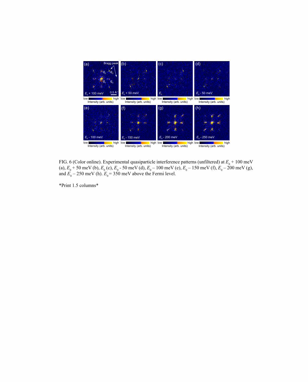
Figure 6 shows raw unfiltered quasiparticle interference patterns obtained by Fourier
transforming the dI/dV maps in Fig. 4. The four bright spots near 3q and the four bright spots in
the middle of the image edges are the Bragg peaks originating from the atomic corrugation of the
underlying SnTe lattice [see arrows in Fig. 6(a)]. The intra-cone scattering 1q wave vector is
located at the center, which is accompanied by intensity from long wavelength modulations from
disorder in the sample. The two pairs of equivalent inter-cone scattering 2q and 3q wave vectors
are also observed at the expected positions. The elongated shape of 2q and 3q indicates the
anisotropy of the surface bands. Although 3'q is also expected according to the schematic in Fig.
9
5, it was not observed. This may be related to matrix element effects resulting in a different
amplitude of 3'q . As the energy is stepped through the zero energy crossing point, the intensity of
the quasiparticle interference patterns decreases first and then increases, with a minimum around
the zero energy crossing point. We also note an intensity asymmetry in the quasiparticle
interference patterns with respect to 2q and
4q , which occurs near the zero energy crossing point
[Figs. 6(b) - 6(d)]. The origin of this asymmetry is unknown at present, but may be due to tip
asymmetries, or rhombohedral distortion in the SnTe atomic lattice.
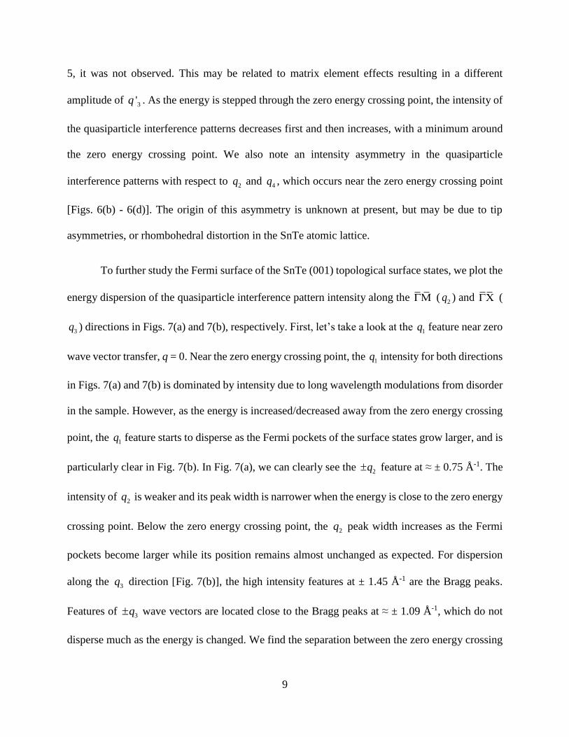
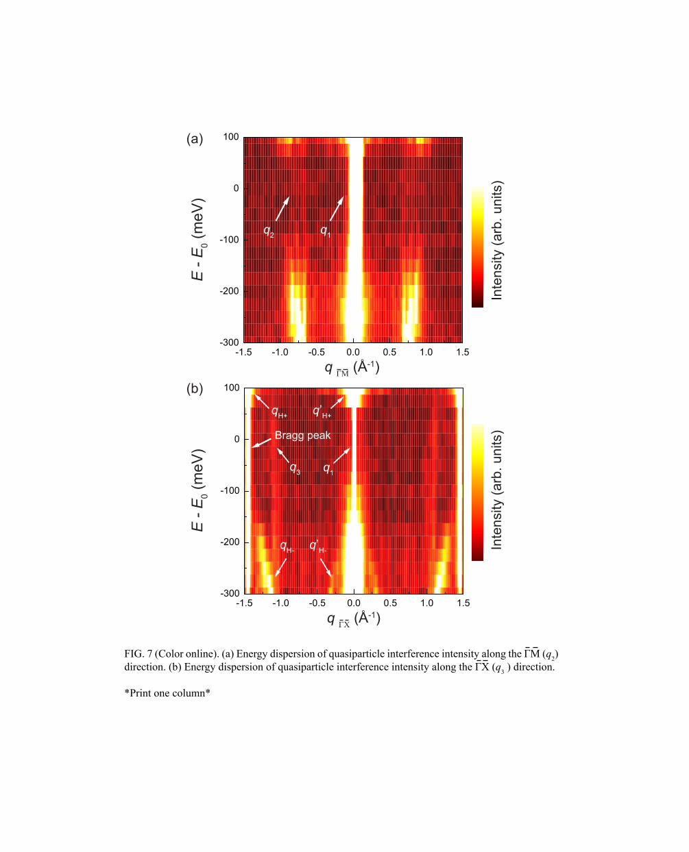
To further study the Fermi surface of the SnTe (001) topological surface states, we plot the
energy dispersion of the quasiparticle interference pattern intensity along the ( 2q ) and (
3q ) directions in Figs. 7(a) and 7(b), respectively. First, let’s take a look at the 1q feature near zero
wave vector transfer, q = 0. Near the zero energy crossing point, the 1q intensity for both directions
in Figs. 7(a) and 7(b) is dominated by intensity due to long wavelength modulations from disorder
in the sample. However, as the energy is increased/decreased away from the zero energy crossing
point, the 1q feature starts to disperse as the Fermi pockets of the surface states grow larger, and is
particularly clear in Fig. 7(b). In Fig. 7(a), we can clearly see the 2q feature at ≈ ± 0.75 Å-1. The
intensity of 2q is weaker and its peak width is narrower when the energy is close to the zero energy
crossing point. Below the zero energy crossing point, the 2q peak width increases as the Fermi
pockets become larger while its position remains almost unchanged as expected. For dispersion
along the 3q direction [Fig. 7(b)], the high intensity features at ± 1.45 Å-1 are the Bragg peaks.
Features of 3q wave vectors are located close to the Bragg peaks at ≈ ± 1.09 Å-1, which do not
disperse much as the energy is changed. We find the separation between the zero energy crossing
10
point 1 and the point in k space to be 0.180 ± 0.003 Å-1,30 which is slightly larger than the
value of 0.15 ± 0.01 Å-1 obtained by ARPES from SnTe bulk crystal.9 The larger 1 distance in
our sample is likely due to the higher p-doping concentration as Ref. [9] shows that less p-doped
samples tend to have smaller 1 distance. At E – E0 ≤ -175 meV, there are two distinct features
near 3q and 1q dispersing in opposite q directions as a function of energy. As we will discuss
below and in Figs. 8 and 9, these two features, noted as Hq and H'q respectively, are related to
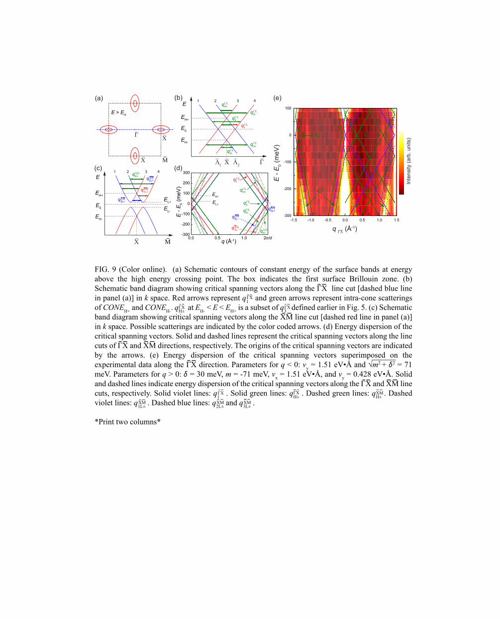
the high energy crossing point beyond the Lifshitz transition energy.
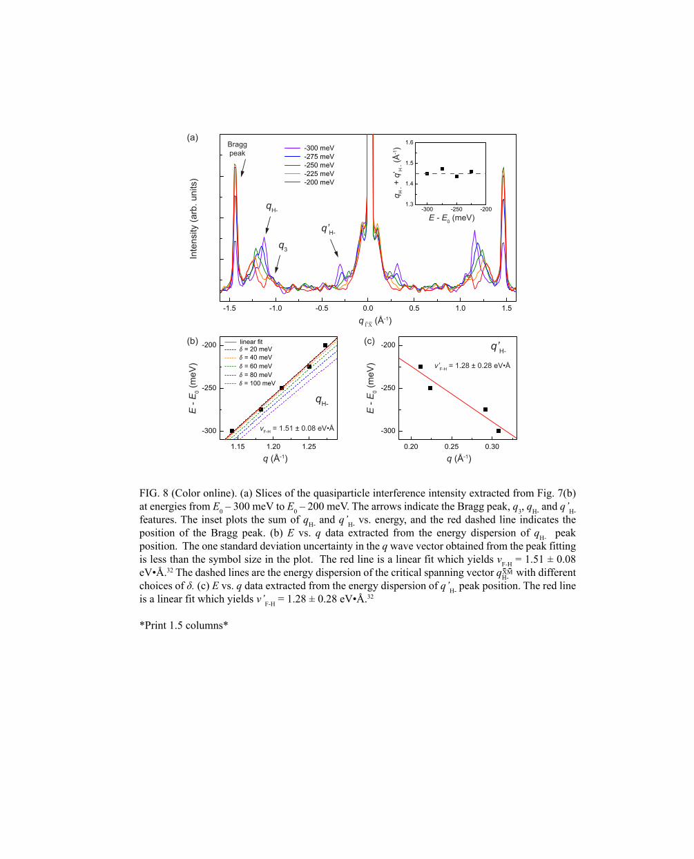
From the energy dispersion of quasiparticle interference pattern intensity plots, we can in
principal extract information about the Fermi velocities along the high symmetry ( 2q and 3q )
directions. However, due to the strong domination of intensity due to disorder near q = 0 at energies
close to the zero energy crossing point, it is not reliable to deduce the Fermi velocities from the q1
wave vector. Instead, we show that the Fermi velocity along the and directions can be
possibly deduced from the Hq and H'q features at energies far away from the zero energy
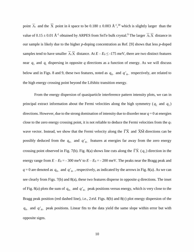
crossing point observed in Fig. 7(b). Fig. 8(a) shows line cuts along the ( 3q ) direction in the
energy range from E – E0 = - 300 meV to E – E0 = - 200 meV. The peaks near the Bragg peak and
q = 0 are denoted as Hq and H'q , respectively, as indicated by the arrows in Fig. 8(a). As we can
see clearly from Figs. 7(b) and 8(a), these two features disperse in opposite q directions. The inset
of Fig. 8(a) plots the sum of Hq and H'q peak positions versus energy, which is very close to the
Bragg peak position (red dashed line), i.e., 2/d. Figs. 8(b) and 8(c) plot energy dispersion of the
Hq and H'q peak positions. Linear fits to the data yield the same slope within error but with
opposite signs.

11
These results suggest that the Hq
and H'q
features originate from the same scattering
mechanism. By examining possible scatterings along the direction above the Lifshitz
transition, we discuss below two possible interpretations of the data in terms of relevant critical
spanning vectors and show these two features can be related to the high energy crossing point
formed when the two neighboring low energy surface bands (1 and
2 ) near the point merge
together. Figure 9(a) shows schematic contours of constant energy of the surface bands above the
high energy crossing point in k space. The box indicates the first surface Brillouin zone. Scattering
along the direction is dominated by the critical spanning vectors along line cuts of (blue
dashed line) and (red dashed line). In the following paragraphs, we will discuss two possible
interpretations for the Hq and H'q features: I. Scattering dominated by the critical spanning
vectors along the line cut; and II. Scattering dominated by the critical spanning vectors along
the line cut.
B - I. Scattering along the line cut
First we focus on the line cut in Fig. 9(b). There are two linear surface bands offset
vertically by 2EH+ in energy at the point. We refer to the cone (pocket from branches 2 and 3)
with the crossing point at EH+ as CONEH+ and the cone (pocket from branches 1 and 4) with the
crossing point at EH- as CONEH- (Unless noted elsewhere, +/- denotes features above/below the
zero energy crossing point). Due to the periodic Brillouin zone boundary conditions, possible
scatterings among the surface bands on the opposite zone boundaries can be reduced to intra-cone
scatterings of CONEH+ ( Hq
, solid green arrows) and CONEH- ( Hq
, solid green arrows). We note
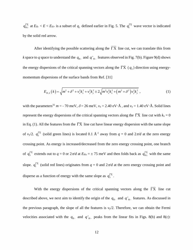
12
Hq
at EH- < E < EH+ is a subset of 3q defined earlier in Fig. 5. The 1q wave vector is indicated
by the solid red arrow.
After identifying the possible scattering along the line cut, we can translate this from
k space to q space to understand the Hq and H'q
features observed in Fig. 7(b). Figure 9(d) shows
the energy dispersions of the critical spanning vectors along the ( 3q ) direction using energy-
momentum dispersions of the surface bands from Ref. [31]
2 2 2 2 2 2 2 2 2 2 2 2 2
, 2H L x x y y x x y yE k m v k v k m v k m v k , (1)
with the parameters31 m = - 70 meV, = 26 meV, vx = 2.40 eV·Å , and vy = 1.40 eV·Å. Solid lines
represent the energy dispersions of the critical spanning vectors along the line cut with kx = 0
in Eq. (1). All the features from the line cut have linear energy dispersion with the same slope
of vy/2. 3q (solid green lines) is located 0.1 Å-1 away from q = 0 and 2/d at the zero energy
crossing point. As energy is increased/decreased from the zero energy crossing point, one branch
of 3q extends out to q = 0 or 2/d at EH± = ± 75 meV and then folds back as Hq
with the same
slope. 1q (solid red lines) originates from q = 0 and 2/d at the zero energy crossing point and
disperse as a function of energy with the same slope as 3q.
With the energy dispersions of the critical spanning vectors along the line cut
described above, we next aim to identify the origin of the Hq and H'q features. As discussed in
the previous paragraph, the slope of all the features is vy/2. Therefore, we can obtain the Fermi
velocities associated with the Hq and H'q peaks from the linear fits in Figs. 8(b) and 8(c):
13
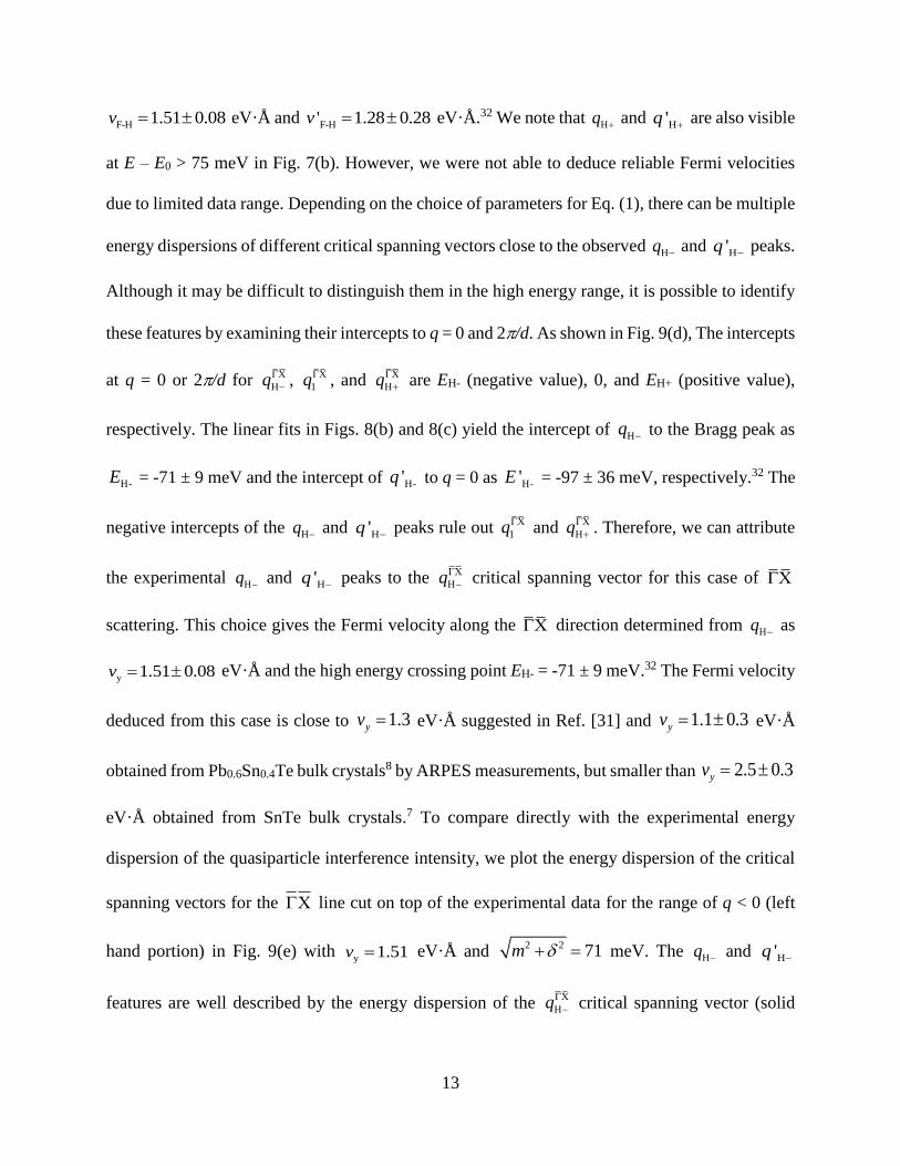
F-H 1.51 0.08v eV·Å and F-H' 1.28 0.28v eV·Å.32 We note that
Hq and
H'q are also visible
at E – E0 > 75 meV in Fig. 7(b). However, we were not able to deduce reliable Fermi velocities
due to limited data range. Depending on the choice of parameters for Eq. (1), there can be multiple
energy dispersions of different critical spanning vectors close to the observed Hq and H'q
peaks.
Although it may be difficult to distinguish them in the high energy range, it is possible to identify
these features by examining their intercepts to q = 0 and 2/d. As shown in Fig. 9(d), The intercepts
at q = 0 or 2/d for Hq
, 1q, and Hq
are EH- (negative value), 0, and EH+ (positive value),
respectively. The linear fits in Figs. 8(b) and 8(c) yield the intercept of Hq to the Bragg peak as
H-E = -71 ± 9 meV and the intercept of H-'q to q = 0 as H-'E = -97 ± 36 meV, respectively.32 The
negative intercepts of the Hq and H'q peaks rule out 1q and Hq
. Therefore, we can attribute
the experimental Hq and H'q peaks to the Hq
critical spanning vector for this case of
scattering. This choice gives the Fermi velocity along the direction determined from Hq as
y 1.51 0.08v eV·Å and the high energy crossing point EH- = -71 ± 9 meV.32 The Fermi velocity
deduced from this case is close to 1.3yv eV·Å suggested in Ref. [31] and 1.1 0.3yv eV·Å
obtained from Pb0.6Sn0.4Te bulk crystals8 by ARPES measurements, but smaller than 2.5 0.3yv
eV·Å obtained from SnTe bulk crystals.7 To compare directly with the experimental energy
dispersion of the quasiparticle interference intensity, we plot the energy dispersion of the critical
spanning vectors for the line cut on top of the experimental data for the range of q < 0 (left
hand portion) in Fig. 9(e) with y 1.51v eV·Å and
2 2 71m meV. The Hq and H'q
features are well described by the energy dispersion of the Hq
critical spanning vector (solid

14
green lines). However, using relations 2 2
1,2 0, / ym v and 2 2
HE m from Ref.
[31], we get 1 = 0.047 ± 0.006 Å-1.33 This value is much smaller than the value of 0.180 ± 0.003
Å-1 obtained from the quasiparticle interference patterns in Fig. 6 and energy dispersion in Fig.
7(b). As indicated in Fig. 9(e) by the arrow, the expected 3q location at the zero energy crossing
point is closer to the Bragg peak than the experimental result.
B - II. Scattering along by the line cut
We next explore the possibility of scattering along the line cut. Figure 9(c) shows the
schematic critical spanning vectors along the line cut. Possible scatterings are indicated by
the color coded arrows: Hq
represents scattering between branches 2 and 3 above EH+; 1Lq
represents scattering between branches 1 and 3 or branches 2 and 4; 2Lq
represents scattering
between branches 1 and 4; and 3Lq
represents scattering between branches 3 and 2 at EL+ < E <
EH+. We note that for EL- < E < EL+, the scattering along the direction for the two separate
cones located symmetrically about the point is essentially a subset of 1q .
Using Eq. (1) with ky = 0 and parameters described above, we plot the energy dispersion
of the critical spanning vectors along the line cut as dashed lines in Fig. 9(d). The Hq
(dashed green lines) originates from q = 0 and 2/d at EH± = ± 75 meV while 1Lq
(dashed red
lines) originates from q = 0 and 2/d at EL± = ± 26 meV. Both 2Lq
and 3Lq
originate at 0.058 Å-
1 away from q = 0 and 2/d at EL± = ± 26 meV. As the energy is moved away from the zero energy
crossing point, 3Lq
extends to q = 0 and 2/d at EH± = ± 75 meV while 1Lq
and 2Lq
features
15
disperse with the same curvature as Hq
. When energy is far away from the zero energy crossing
point (E – E0 >> ), Hq
, 1Lq
, and 2Lq
for the line cut have a nearly linear energy
dispersion with a slope ≈ vx/2. Similar to the case of scattering, we can distinguish these three
features by examining their intercepts to q = 0 and 2/d. Linear extrapolation of the high energy
features of Hq
, 1L-q, and 2L-q
to q = 0 or 2/d gives m (negative value), 0, and -m (positive
value), respectively. The negative intercepts of the Hq and H'q peaks rule out 1L-q and 2L-q
.
Therefore, we can attribute the experimental Hq and H'q peaks to the Hq
critical spanning
vector for this case of scattering and get the Fermi velocity along the direction
x 1.51 0.08v eV·Å from the slope and m = -71 ± 9 meV from the intercept. We can then get the
Fermi velocity along the direction vy as a function of the Lifshitz transition energy using
2 2
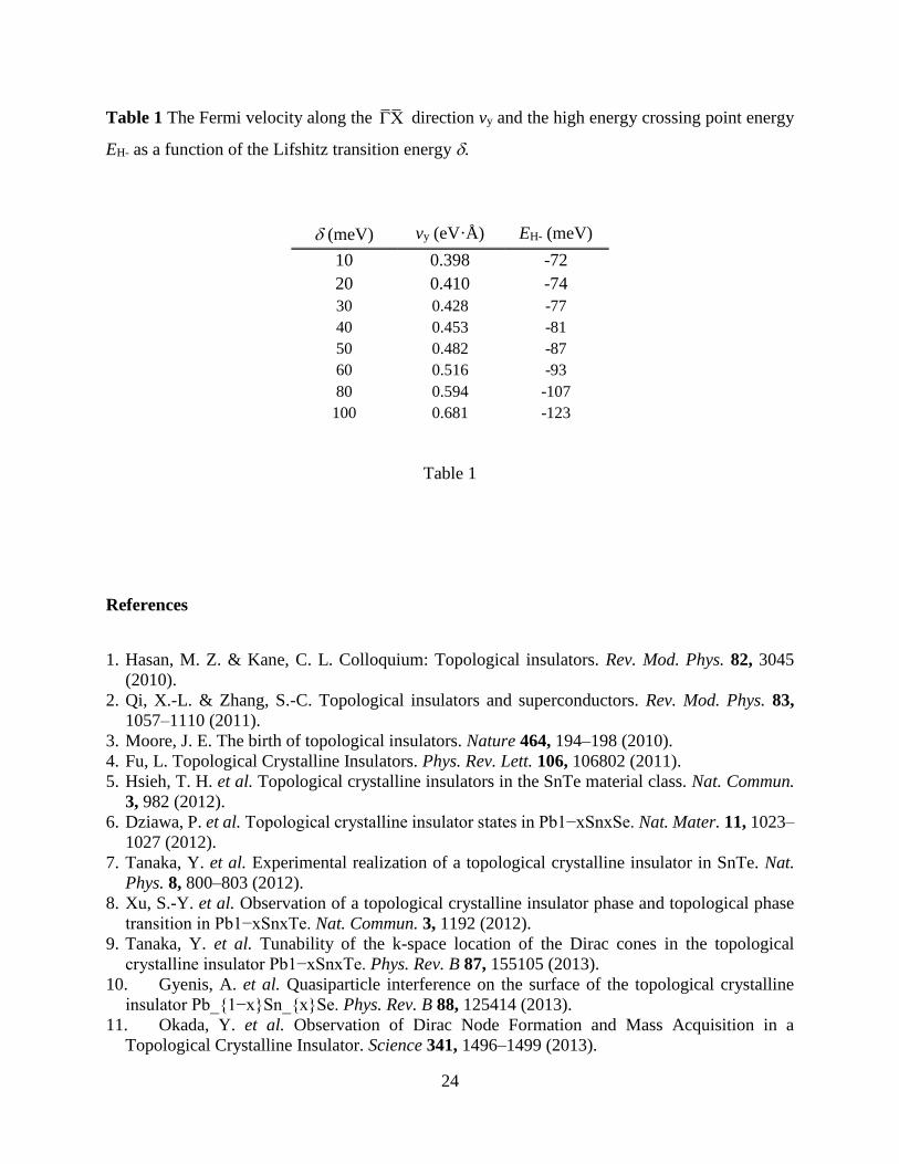
1,2/yv m , where m = -71 ± 9 meV and 1,2 0.180 0.003 Å-1.30 Table 1 shows vy
and EH- as a function of . To determine a range of that is consistent with our data, we plot the
energy dispersion of the critical spanning vector Hq
with different choices of as dashed lines
in Fig. 8(b). The plots follow the data for = 20 meV and 40 meV, but start to deviate from the
data for 60 meV. Therefore, we determine the range of the Lifshitz transition energy to be
≈ 0 meV to 60 meV. With both vx and vy deduced from our data, we plot the energy dispersions of
the critical spanning vectors for both (solid lines) and (dashed lines) line cuts on top of
the experimental data for the range of q > 0 (right hand portion) in Fig. 9(e), with = 30 meV, m
= -71 meV, x 1.51v eV·Å, and 0.428yv eV·Å. Now the q location of the 3q feature at the
zero energy crossing point is consistent with our data and the Hq and H'q peaks are well
16
described by the energy dispersion of the Hq
critical spanning vector (dashed green lines). The
domination of the Hq
features over the Hq
features can be expected because of the better nesting
of the Fermi surface along the direction. However, we did not observe any strong energy
dependence of the other features such as 1q and 3q as suggested by the critical spanning vectors.
We also note the Fermi velocities deduced from our data for this case is much smaller than those
obtained from ARPES measurements7,8.
In summary, both cases of scattering along the and line cuts can describe the
observed Hq and H'q features. However, neither explains our data completely. The case for the
scattering would indicate that the 3q features are closer to the Bragg peaks than what was
observed in our quasiparticle interference patterns. The case for the scattering would indicate
smaller Fermi velocities than those reported in the literature7,8,31, which give rise to strong energy
dependent q features and interconnected patterns at high energies [see Figs. 9(e) and 10] that were
not observed in the data. Therefore it is likely that the actual scattering interference phenomena
observed in STS measurements has contributions from both of these extreme cases. In the next
section, we will simulate quasiparticle interference patterns to shine light on these two possible
interpretations.

17
C. Surface states spin texture
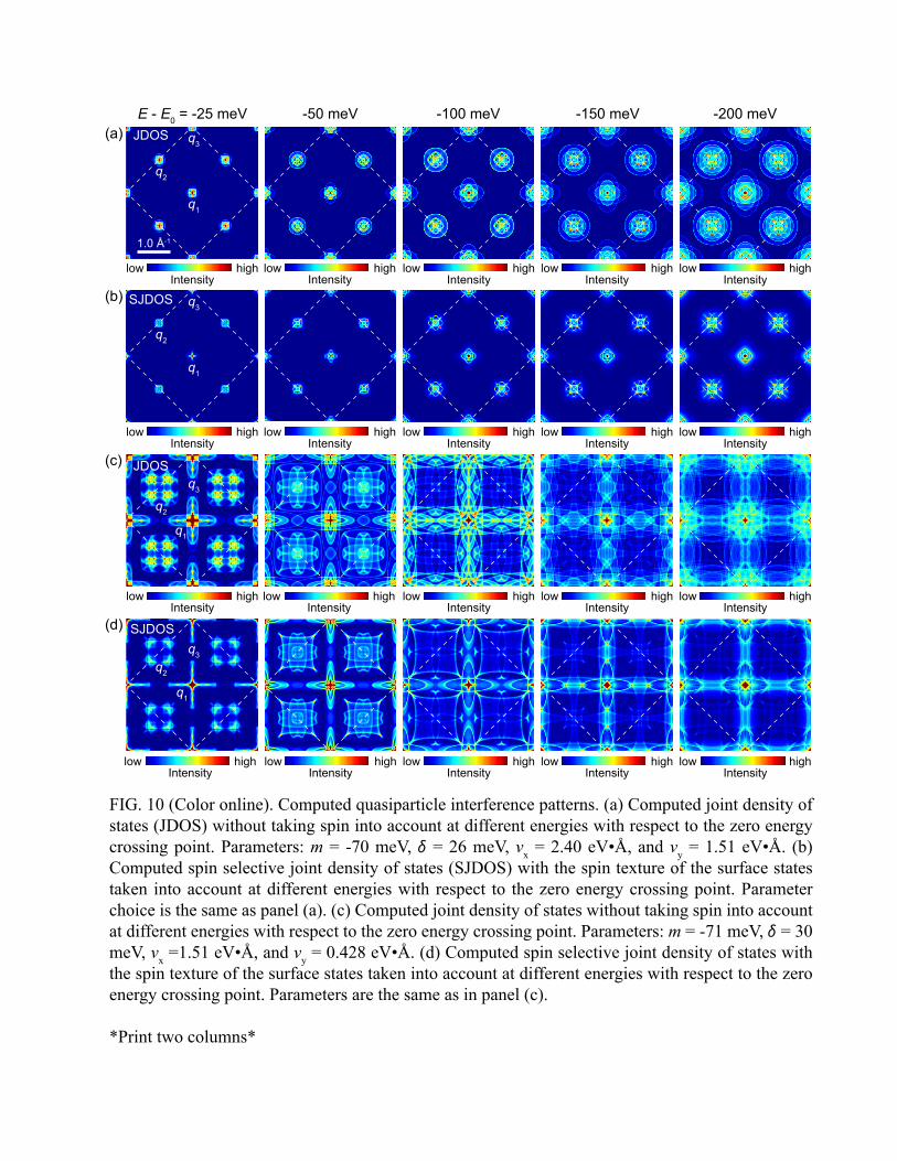
To probe the possible spin textures at the surface, we have also carried out calculations of
the joint density of states. The joint density of states is closely related to quasiparticle interference
patterns because scattering q wave vectors that connect regions of high density of states on the
contours of constant energy contribute to a large degree in the joint density of states maps. The
joint density of states is computed by taking the autoconvolution of the initial and final scattering
states29
2( , ) ( , ) ( , )JDOS E E E d q k k q k , (2)
where ( , )E k and ( , )E k q are the initial and final density of states. The density of states for
Eq. (2) is obtained as a constant around the contours of constant energy derived from the energy-
momentum dispersions of the surface bands described by Equation (1). To compare the calculation
with our experimental data, we show the computed joint density of states in Figs. 10(a) and 10(c)
for different energies away from the zero energy crossing point. For the case of scattering along
the line cut [Fig. 10(a)], we cannot obtain vx directly from our data. But given that our
experimental values of y 1.51 0.08v eV·Å and
2 2 71 9m meV are close to vy = 1.30
eV·Å and 2 2 75m meV in Ref. [31], it is reasonable to choose m = -70 meV, = 26 meV,
and x 2.40v eV·Å from Ref. [31] with an experimental value of y 1.51v eV·Å for the joint
density of states calculation to have a qualitative comparison with the experimental quasiparticle
interference patterns. As for the case of scattering along the line cut [Fig. 10(c)], we choose
m = -71 meV, = 30 meV, x 1.51v eV·Å, and 0.428yv eV·Å obtained from our data. The
white dashed boxes indicate the first scattering zones with a size of 4/d × 4/d. The calculation

18
suggests a rich structure in the quasiparticle interference patterns. When the energy is decreased
from the zero energy crossing point, the general trend is that the disk size for all the q wave vectors
becomes larger as the surface state Fermi pockets grow larger. The calculated patterns using the
smaller Fermi velocities obtained from the scattering [Fig. 10(c)] generally have a larger disk
size compared to those obtained with larger Fermi velocities in Fig. 10 (a). Fig. 10(c) also shows
that different q features such as 1q and 3q become interconnected to each other for energies far
away from the zero energy crossing point.
To understand the impact of the spin-momentum locked surface states on the scattering
process, we also take the spin texture into account and compute the spin selective joint density of
states following Ref. [29],
2( ) ( ) ( , ) ( )SJDOS T d q k q k k q k , (3)
where ( , )T q k is the spin-dependent scattering matrix element. We model the spin texture as simple
artificial momentum-locked spins that are tangential to the contours of constant energy. Due to the
spin-momentum locking mechanism, the scattering process is suppressed for the unaligned spins
and forbidden for oppositely aligned spins. Thus, this spin-dependent scattering causes the
quasiparticle interference pattern to differ from the one obtained from the joint density of states
without considering spin directions. As shown in Figs. 10(b) and 10(d), the computed spin
selective joint density of states with the same two sets of parameters obviously contrast the
corresponding ones obtained from the joint density of states. The spin selective joint density of
states disk size for 2q and 3q is smaller over the entire energy range compared to that of the joint
density of states, which indicates reduced scattering at the surface. Furthermore, the changed shape
of the q vectors as compared to that of the joint density of states also suggests reduced intra- and

19
inter-cone scattering. A direct comparison between the experimental and computed quasiparticle
interference patterns suggests the choice of larger Fermi velocities for the surface bands (the
scattering case) agrees better with our experimental quasiparticle interference patterns though the
observed 1 value is larger than expected based on the model in Ref. [31]. This discrepancy
may be related to the warping in the Fermi surface of the surface bands and/or the limitation of the
model. The small disk size of 2q and 3q in our experimental quasiparticle interference patterns
also suggests reduced scattering at the surface, possibly due to the spin-momentum locked
topological surface states. However, the relatively weak scattering from defects, smearing of
features due to surface disorder, and high doping concentration in our sample preclude a definitive
confirmation of the spin texture of the surface states. Further measurements on samples with very
low doping concentration are necessary to confirm the spin texture of the SnTe topological surface
states.
IV. Conclusions
In conclusion, we have synthesized single crystalline SnTe nanoplates on graphitized 6H-
SiC substrates by MBE and carried out in-situ STM measurements on the (001) surface states. Our
observation of the quasiparticle interference patterns is consistent with scattering among the four
Fermi pockets of the surface states in the first surface Brillouin zone. The energy dispersion of the
quasiparticle interference intensity shows two high energy features related to the crossing point
beyond the Lifshitz transition when the two neighboring low energy surface bands near the
point merge. We have presented two possible interpretations for the two high energy features due
to different scattering vectors. A comparison between the experimental and computed quasiparticle
interference patterns seems to suggest the case of scattering agrees better with our data as well

20
as possible spin texture of the surface states. This work demonstrates that SnTe nanoplates can
provide a model system for studying topological crystalline insulator surface states and exploring
potential device applications.
Acknowledgement
We thank Liang Fu, Mark Stiles, and Guru Khalsa for valuable comments and discussions.
We are also grateful to Takafumi Sato and Yoichi Ando for sharing with us the SnTe (001) surface
state parameters estimated from their ARPES measurements. D. Z., J. H., and T. Z. acknowledge
support under the Cooperative Research Agreement between the University of Maryland and the
National Institute of Standards and Technology Center for Nanoscale Science and Technology,
Grant No. 70NANB10H193, through the University of Maryland. H. B. and Y. K. are partly
supported by Korea Research Foundation through Grant No. KRF-2010-00349.
Table Captions
Table 1 The Fermi velocity along the direction vy and the high energy crossing point energy
EH- as a function of the Lifshitz transition energy .
Figure Captions
Fig. 1 (Color online). Synthesis and characterization of SnTe nanoplates. (a) Schematic of the
SnTe rock salt structure. (b) RHEED pattern from SnTe nanoplates during MBE growth. (c) AFM
image of as grown SnTe nanoplates. (d) XRD from SnTe nanoplates confirms single crystal nature
showing only {001} reflections. The asterisks indicate the {0001} reflections of the SiC substrate.
Fig. 2 (Color online). (a) A 100 nm × 100 nm STM topographic image showing terraces with step
height of one half unit cell (≈ 0.32 nm). The color scale covers a height range of 1.15 nm. (b) A
typical 55 nm × 55 nm STM topographic image at the (001)-terminated surface of a SnTe
nanoplate, tunneling setpoint: Vbias = 0.8 V and I = 100 pA. The color scale covers a height range

21
of 98 pm. (c) Schematic SnTe (001) surface state band structure. The first surface Brillouin zone
is indicated by the shaded square. (d) Single point dI/dV spectrum, tunneling setpoint: Vbias = 0.7
V and I = 150 pA. Inset shows a simplified schematic band diagram of the two low energy surface
bands located symmetrically about the point along direction. E0 denotes the zero energy
crossing point and EH± denotes the high energy crossing points beyond the Lifshitz transition. Blue
and red lines indicate opposite spin orientations.
Fig. 3 (Color online). Atomic defects on the SnTe (001) surface. (a) and (c) Experimental high-
resolution topographic images of atomic defects on the SnTe (001) surface at I = 70 pA and
different sample biases. The color scale range is 65 pm for Vbias = 1.0 V, 60 pm for Vbias = 0.8 V,
65 pm for Vbias = 0.6 V, 70 pm for Vbias = 0.4 V, 40 pm for Vbias = - 0.8 V, 50 pm for Vbias = - 0.6 V,
60 pm for Vbias = - 0.4 V, and 55 pm for Vbias = - 0.2 V. The Sn vacancies are indicated by red
arrows and other types of defects are indicated by green arrows in image Vbias = 1.0 V. The dashed
lines indicate the Te atom site positions. (b) and (d) DFT simulated topographic images with Sn
vacancies at different sample biases. The color scale range is 162 pm and the dashed lines indicate
the Te atom site positions.
Fig. 4 (Color online). dI/dV spatial maps of a 47.5 nm × 47.5 nm area at different energies with
respect to the zero energy crossing point E0, which is 350 meV above the Fermi level.
Fig. 5 (Color online). Quasiparticle interference at the SnTe (001) surface. (a) Schematic of SnTe
(001) surface band structure at energies below the Lifshitz transition in the first surface Brillouin
zone. q1 represents intra-cone scattering; q2, q3, and q4 represent inter-cone scattering. (b)
Schematic contours of constant energy near the zero energy crossing point in the first surface
Brillouin zone. q vectors are indicated by the color coded arrows. Due to periodic Brillouin zone
boundary condition, 3q is equivalent to 3'q , the inter-cone scattering across the first surface
Brillouin zone boundary. (c) Schematic quasiparticle interference pattern enclosed by a box with
size of 4π/d × 4π/d in q space.

22
Fig. 6 (Color online). Experimental quasiparticle interference patterns (unfiltered) at E0 + 100 meV
(a), E0 + 50 meV (b), E0 (c), E0 - 50 meV (d), E0 – 100 meV (e), E0 – 150 meV (f), E0 – 200 meV
(g), and E0 – 250 meV (h). E0 = 350 meV above the Fermi level.
Fig. 7 (Color online). (a) Energy dispersion of quasiparticle interference intensity along the
( 2q ) direction. (b) Energy dispersion of quasiparticle interference intensity along the ( 3q )
direction.
Fig. 8 (Color online). (a) Slices of the quasiparticle interference intensity extracted from Fig. 7(b)
at energies from E0 – 300 meV to E0 – 200 meV. The arrows indicate the Bragg peak, 3q , Hq and
H'q features. The inset plots the sum of Hq and H'q vs. energy, and the red dashed line indicates
the position of the Bragg peak. (b) E vs. q data extracted from the energy dispersion of Hq peak
position. The one standard deviation uncertainty in the q wave vector obtained from the peak
fitting is less than the symbol size in the plot. The red line is a linear fit which yields vF-H = 1.51
± 0.08 eV·Å.32 The dashed lines are the energy dispersion of the critical spanning vector Hq
with
different choices of (c) E vs. q data extracted from the energy dispersion of H'q peak position.
The red line is a linear fit which yields vF-H = 1.28 ± 0.28 eV·Å.32
Fig. 9 (Color online). (a) Schematic contours of constant energy of the surface bands at energy
above the high energy crossing point. The box indicates the first surface Brillouin zone. (b)
Schematic band diagram showing critical spanning vectors along the line cut [dashed blue
line in panel (a)] in k space. Red arrows represent 1q and green arrows represent intra-cone
scatterings of CONEH+ and CONEH-. Hq
at EH- < E < EH+ is a subset of 3q defined earlier in Fig.
5. (c) Schematic band diagram showing critical spanning vectors along the line cut [dashed
red line in panel (a)] in k space. Possible scatterings are indicated by the color coded arrows. (d)
Energy dispersion of the critical spanning vectors. Solid and dashed lines represent the critical
spanning vectors along the line cuts of and directions, respectively. The origins of the
critical spanning vectors are indicated by the arrows. (e) Energy dispersion of the critical spanning
vectors superimposed on the experimental data along the direction. Parameters for q < 0:

23
y 1.51v eV·Å and 2 2 71m meV. Parameters for q > 0: = 30 meV, m = -71 meV,
x 1.51v eV·Å, and 0.428yv eV·Å. Solid and dashed lines indicate energy dispersion of the
critical spanning vectors along the and line cuts, respectively. Solid violet lines: 1q.
Solid green lines: Hq
. Dashed green lines: Hq
. Dashed violet lines: 1Lq
. Dashed blue lines:
2Lq
and 3Lq
.
Fig. 10 (Color online). Computed quasiparticle interference patterns. (a) Computed joint density
of states (JDOS) without taking spin into account at different energies with respect to the zero
energy crossing point. Parameters: m = -70 meV, = 26 meV, x 2.40v eV·Å, and 1.51yv
eV·Å. (b) Computed spin selective joint density of states (SJDOS) with the spin texture of the
surface states taken into account at different energies with respect to the zero energy crossing point.
Parameter choice is the same as panel (a). (c) Computed joint density of states without taking spin
into account at different energies with respect to the zero energy crossing point. Parameters: m = -
71 meV, = 30 meV, x 1.51v eV·Å, and 0.428yv eV·Å. (d) Computed spin selective joint
density of states with the spin texture of the surface states taken into account at different energies
with respect to the zero energy crossing point. Parameters are the same as in panel (c).
24
Table 1 The Fermi velocity along the direction vy and the high energy crossing point energy
EH- as a function of the Lifshitz transition energy .
(meV) vy (eV·Å) EH- (meV)
10 0.398 -72
20 0.410 -74
30 0.428 -77
40 0.453 -81
50 0.482 -87
60 0.516 -93
80 0.594 -107
100 0.681 -123
Table 1
References
1. Hasan, M. Z. & Kane, C. L. Colloquium: Topological insulators. Rev. Mod. Phys. 82, 3045
(2010).
2. Qi, X.-L. & Zhang, S.-C. Topological insulators and superconductors. Rev. Mod. Phys. 83,
1057–1110 (2011).
3. Moore, J. E. The birth of topological insulators. Nature 464, 194–198 (2010).
4. Fu, L. Topological Crystalline Insulators. Phys. Rev. Lett. 106, 106802 (2011).
5. Hsieh, T. H. et al. Topological crystalline insulators in the SnTe material class. Nat. Commun.
3, 982 (2012).
6. Dziawa, P. et al. Topological crystalline insulator states in Pb1−xSnxSe. Nat. Mater. 11, 1023–
1027 (2012).
7. Tanaka, Y. et al. Experimental realization of a topological crystalline insulator in SnTe. Nat.
Phys. 8, 800–803 (2012).
8. Xu, S.-Y. et al. Observation of a topological crystalline insulator phase and topological phase
transition in Pb1−xSnxTe. Nat. Commun. 3, 1192 (2012).
9. Tanaka, Y. et al. Tunability of the k-space location of the Dirac cones in the topological
crystalline insulator Pb1−xSnxTe. Phys. Rev. B 87, 155105 (2013).
10. Gyenis, A. et al. Quasiparticle interference on the surface of the topological crystalline
insulator Pb_{1−x}Sn_{x}Se. Phys. Rev. B 88, 125414 (2013).
11. Okada, Y. et al. Observation of Dirac Node Formation and Mass Acquisition in a
Topological Crystalline Insulator. Science 341, 1496–1499 (2013).
25
12. Zeljkovic, I. et al. Mapping the unconventional orbital texture in topological crystalline
insulators. ArXiv13120164 Cond-Mat (2013). at <http://arxiv.org/abs/1312.0164>
13. Taskin, A. A., Sasaki, S., Segawa, K. & Ando, Y. Topological Surface Transport in
Epitaxial SnTe Thin Films Grown on Bi2Te3. ArXiv13052470 Cond-Mat (2013). at
<http://arxiv.org/abs/1305.2470>
14. Safdar, M. et al. Topological Surface Transport Properties of Single-Crystalline SnTe
Nanowire. Nano Lett. 13, 5344–5349 (2013).
15. Peng, H. et al. Aharonov-Bohm interference in topological insulator nanoribbons. Nat.
Mater. 9, 225–229 (2010).
16. Zhang, D. et al. Superconducting proximity effect and possible evidence for Pearl vortices
in a candidate topological insulator. Phys. Rev. B 84, 165120 (2011).
17. Veldhorst, M. et al. Josephson supercurrent through a topological insulator surface state.
Nat. Mater. 11, 417–421 (2012).
18. Kandala, A. et al. Growth and characterization of hybrid insulating ferromagnet-
topological insulator heterostructure devices. Appl. Phys. Lett. 103, 202409 (2013).
19. Song, Y. J. et al. Invited Review Article: A 10 mK scanning probe microscopy facility.
Rev. Sci. Instrum. 81, 121101–121101–33 (2010).
20. Mortensen, J. J., Hansen, L. B. & Jacobsen, K. W. Real-space grid implementation of the
projector augmented wave method. Phys. Rev. B 71, 035109 (2005).
21. Enkovaara, J. et al. Electronic structure calculations with GPAW: a real-space
implementation of the projector augmented-wave method. J. Phys. Condens. Matter 22, 253202
(2010).
22. Bahn, S. R. & Jacobsen, K. W. An Object-Oriented Scripting Interface to a Legacy
Electronic Structure Code. Comput. Sci. Eng. 4, 56–66 (2002).
23. Perdew, J. P., Burke, K. & Ernzerhof, M. Generalized Gradient Approximation Made
Simple. Phys. Rev. Lett. 77, 3865–3868 (1996).
24. Perdew, J. P., Burke, K. & Ernzerhof, M. Generalized Gradient Approximation Made
Simple [Phys. Rev. Lett. 77, 3865 (1996)]. Phys. Rev. Lett. 78, 1396–1396 (1997).
25. Crommie, M. F., Lutz, C. P. & Eigler, D. M. Imaging standing waves in a two-dimensional
electron gas. Nature 363, 524–527 (1993).
26. Hoffman, J. E. et al. Imaging Quasiparticle Interference in Bi2Sr2CaCu2O8+δ. Science
297, 1148–1151 (2002).
27. Rutter, G. M. et al. Scattering and Interference in Epitaxial Graphene. Science 317, 219–
222 (2007).
28. Mallet, P. et al. Role of pseudospin in quasiparticle interferences in epitaxial graphene
probed by high-resolution scanning tunneling microscopy. Phys. Rev. B 86, 045444 (2012).
29. Roushan, P. et al. Topological surface states protected from backscattering by chiral spin
texture. Nature 460, 1106–1109 (2009).
30. The error is one standard deviation uncertainty determined from the Gaussian peak fit of
the q3 feature in Fig. 7(b).
31. Liu, J., Duan, W. & Fu, L. Surface States of Topological Crystalline Insulators in IV-VI
Semiconductors. arXiv:1304.0430 (2013). at <http://arxiv.org/abs/1304.0430>
32. The errors are one standard deviation uncertainty determined from the linear fits of the
data.
33. The error is determined from the error propagation of the measured quantities.
(a)
Sn Te a = 0.63 nm
d = 0.45 nm
hh0
h00(b)
(c)
2 μm
0 78 nm
002
004
006* *
* *
* * *
(d)
FIG. 1 (Color online). Synthesis and characterization of SnTe nanoplates. (a) Schematic of the SnTe rock salt structure. (b) RHEED pattern from SnTe nanoplates during MBE growth. (c) AFM image of as grown SnTe nanoplates. (d) XRD from SnTe nanoplates confirms single crystal nature showing only {001} reflections. The asterisks indicate the {0001} reflections of the SiC substrate.
*Print one column*
10 nm
(a) (b)
10 nm
Χ
Γ
Μ
Λ1Λ2
(c) (d) E
E0
ΧΓ Γ
EH+
EH-
FIG. 2 (Color online). (a) A 100 nm × 100 nm STM topographic image showing terraces with step height of one half unit cell (≈ 0.32 nm). The color scale covers a height range of 1.15 nm. (b) A typical 55 nm × 55 nm STM topographic image at the (001)-terminated surface of a SnTe nanoplate, tunneling setpoint: Vbias = 0.8 V and I = 100 pA. The color scale covers a height range of 98 pm. (c) Schematic SnTe (001) surface state band structure. The first surface Brillouin zone is indicated by the shaded square. (d) Single point dI/dV spectrum, tunneling setpoint: Vbias = 0.7 V and I = 150 pA. Inset shows a simplified schematic band diagram of the two low energy surface bands located symmetrically about the Χ point along ГΧ direction. E0 denotes the zero energy crossing point and EH± denotes the high energy crossing points beyond the Lifshitz transition. Blue and red lines indicate opposite spin orientations.
*Print one column*
(a) 1.0 V
1 nm
0.8 V 0.6 V 0.4 V
(b) 1.0 V
1 nm
0.8 V 0.6 V 0.4 V
(c) -0.2 V-0.4 V-0.6V-0.8V
1 nm
(d) - 0.2 V- 0.4 V- 0.6 V- 0.8 V
1 nm
FIG. 3 (Color online). Atomic defects on the SnTe (001) surface. (a) and (c) Experimental high-resolution topographic images of atomic defects on the SnTe (001) surface at I = 70 pA and different sample biases. The color scale range is 65 pm for Vbias = 1.0 V, 60 pm for Vbias = 0.8 V, 65 pm for Vbias = 0.6 V, 70 pm for Vbias = 0.4 V, 40 pm for Vbias = - 0.8 V, 50 pm for Vbias = - 0.6 V, 60 pm for Vbias = - 0.4 V, and 55 pm for Vbias = - 0.2 V. The Sn vacancies are indicated by red arrows and other types of defects are indicated by green arrows in image Vbias = 1.0 V. The dashed lines indicate the Te atom site positions. (b) and (d) DFT simulated topographic images with Sn vacancies at different sample biases. The color scale range is 162 pm and the dashed lines indicate the Te atom site positions.
*Print 1.5 columns*
E0 + 100 meV 5 nm
0 166dI/dV (pS)
(a)
E0 + 50 meV
0 104dI/dV (pS)
(b)
E0
0 100dI/dV (pS)
(c)
E0 - 50 meV
0 102dI/dV (pS)
(d)
E0 - 100 meV
0 102dI/dV (pS)
(e)
E0 - 150 meV
0 109dI/dV (pS)
(f)
E0 - 200 meV
0 133dI/dV (pS)
(g)
E0 - 250 meV
0 152dI/dV (pS)
(h)
FIG. 4 (Color online). dI/dV spatial maps of a 47.5 nm × 47.5 nm area at different energies with respect to the zero energy crossing point E0, which is 350 meV above the Fermi level.
*Print 1.5 columns*
q1q4
q3
q2
Γ
Χ
Μ
k space
Λ1
(a)
k space
q1
q3
q2
q4
Μ
Χ
(0, /
d)
(0, -
/d)(-/d, 0)
(/d, 0)
Γ
q’3
(b) q space
(0, 2
/d)
(0, -2/d
)(-2/d, 0)
(2/d, 0)
q1
q3q2
q4
q’3
(c)
FIG. 5 (Color online). Quasiparticle interference at the SnTe (001) surface. (a) Schematic of SnTe (001) surface band structure at energies below the Lifshitz transition in the first surface Brillouin zone. q1 represents intra-cone scattering; q2, q3, and q4 represent inter-cone scattering. (b) Schematic contours of constant energy near the zero energy crossing point in the first surface Brillouin zone. q vectors are indicated by the color coded arrows. Due to periodic Brillouin zone boundary condition, q3 is equivalent to q’3, the inter-cone scattering across the first surface Brillouin zone boundary. (c) Schematic quasiparticle interference pattern enclosed by a box with size of 4π/d × 4π/d in q space.
*Print one column*
E0 + 100 meV 0.5 Å-1
q1
q2 q3
q4
Bragg peak
low highIntensity (arb. units)
(a)
E0 + 50 meV
low highIntensity (arb. units)
(b)
E0
low highIntensity (arb. units)
(c)
E0 - 50 meV
low highIntensity (arb. units)
(d)
E0 - 100 meV
low highIntensity (arb. units)
(e)
E0 - 150 meVlow high
Intensity (arb. units)
(f)
E0 - 200 meV
low highIntensity (arb. units)
(g)
E0 - 250 meV
low highIntensity (arb. units)
(h)
FIG. 6 (Color online). Experimental quasiparticle interference patterns (unfiltered) at E0 + 100 meV (a), E0 + 50 meV (b), E0 (c), E0 - 50 meV (d), E0 – 100 meV (e), E0 – 150 meV (f), E0 – 200 meV (g), and E0 – 250 meV (h). E0 = 350 meV above the Fermi level.
*Print 1.5 columns*
(a)
E -
E0 (
meV
)
Inte
nsity
(arb
. uni
ts)
q2 q1
q ΓΜ (Å-1)(b)
E -
E0 (
meV
)
Bragg peak
Inte
nsity
(arb
. uni
ts)
qH- q’H-
q3 q1
q ΓΧ (Å-1)
qH+ q’H+
FIG. 7 (Color online). (a) Energy dispersion of quasiparticle interference intensity along the ГΜ (q2) direction. (b) Energy dispersion of quasiparticle interference intensity along the ГΧ (q3 ) direction.
*Print one column*
(c)
E -
E0 (
meV
)
q (Å-1)
q’H-
v’F-H = 1.28 ± 0.28 eV•Å
(b)
E -
E0 (
meV
)
q (Å-1)
qH-
vF-H = 1.51 ± 0.08 eV•Å
linear fit = 20 meV
= 100 meV = 80 meV = 60 meV = 40 meV
(a)
Inte
nsity
(arb
. uni
ts)
Braggpeak
qH-
q ΓΧ (Å-1)
E - E0 (meV)
q H - +
q’ H
- (Å-1
)
q3
q’H-
FIG. 8 (Color online). (a) Slices of the quasiparticle interference intensity extracted from Fig. 7(b) at energies from E0 – 300 meV to E0 – 200 meV. The arrows indicate the Bragg peak, q3, qH- and q’H- features. The inset plots the sum of qH- and q’H- vs. energy, and the red dashed line indicates the position of the Bragg peak. (b) E vs. q data extracted from the energy dispersion of qH- peak position. The one standard deviation uncertainty in the q wave vector obtained from the peak fitting is less than the symbol size in the plot. The red line is a linear fit which yields vF-H = 1.51 ± 0.08 eV•Å.32 The dashed lines are the energy dispersion of the critical spanning vector qH- with different choices of δ. (c) E vs. q data extracted from the energy dispersion of q’H- peak position. The red line is a linear fit which yields v’F-H = 1.28 ± 0.28 eV•Å.32
*Print 1.5 columns*
ΧΜ
Χ
(a)
Μ
Γ
E > EH
Χ
(b)
Χ ΓΛ2Λ1
E
EH+
E0
EH-
1 2 3 4qH+ΓΧ
qH-ΓΧ
q3ΓΧ
q1ΓΧ
qH-ΓΧ
qH+ΓΧ
1 2 3 4(c)
Χ
E
EH+
E0
EH-
EL+
EL-
Μ
q3L+
qH+ΧΜ
q2L+ΧΜ
ΧΜ
q1L+ΧΜ
q3ΓΧ
EH+
EL+
q2L-ΧΜ
q1L-ΧΜ
E -
E0 (
meV
)
q (Å-1)
q1ΓΧ
qH+ΓΧ
qH-ΓΧ q3L+
ΧΜ
qH-ΧΜ
2/d
(d)
(e)
E -
E0 (
meV
)
Inte
nsity
(arb
. uni
ts)
q ΓΧ (Å-1)
q3 q3
qH-ΓΧ qH-
ΧΜ
FIG. 9 (Color online). (a) Schematic contours of constant energy of the surface bands at energy above the high energy crossing point. The box indicates the first surface Brillouin zone. (b) Schematic band diagram showing critical spanning vectors along the ГΧ line cut [dashed blue line in panel (a)] in k space. Red arrows represent q1 and green arrows represent intra-cone scatterings of CONEH+ and CONEH-. qH± at EH- < E < EH+ is a subset of q3 defined earlier in Fig. 5. (c) Schematic band diagram showing critical spanning vectors along the ΧΜ line cut [dashed red line in panel (a)] in k space. Possible scatterings are indicated by the color coded arrows. (d) Energy dispersion of the critical spanning vectors. Solid and dashed lines represent the critical spanning vectors along the line cuts of ГΧ and ΧΜ directions, respectively. The origins of the critical spanning vectors are indicated by the arrows. (e) Energy dispersion of the critical spanning vectors superimposed on the experimental data along the ГΧ direction. Parameters for q < 0: vy = 1.51 eV•Å and √m2 + 2 = 71 meV. Parameters for q > 0: = 30 meV, m = -71 meV, vx = 1.51 eV•Å, and vy = 0.428 eV•Å. Solid and dashed lines indicate energy dispersion of the critical spanning vectors along the ГΧ and ΧΜ line cuts, respectively. Solid violet lines: q1 . Solid green lines: qH± . Dashed green lines: qH± . Dashed violet lines: q1L± . Dashed blue lines: q2L± and q3L± .
*Print two columns*
ГΧ
ГΧ ГΧ
ГΧГΧ ΧΜ
ΧΜ ΧΜΧΜ
(a) JDOS
q1
q2
q3
E - E0 = -25 meV -50 meV -100 meV -200 meV-150 meV
1.0 Å-1
low highIntensity
low highIntensity
low highIntensity
low highIntensity
low highIntensity
(b) SJDOS
q1
q2
q3
low highIntensity
low highIntensity
low highIntensity
low highIntensity
low highIntensity
(c) JDOSq3
q1
q2
low highIntensity
low highIntensity
low highIntensity
low highIntensity
low highIntensity
(d) SJDOS
q2
q3
q1
low highIntensity
low highIntensity
low highIntensity
low highIntensity
low highIntensity
FIG. 10 (Color online). Computed quasiparticle interference patterns. (a) Computed joint density of states (JDOS) without taking spin into account at different energies with respect to the zero energy crossing point. Parameters: m = -70 meV, = 26 meV, vx = 2.40 eV•Å, and vy = 1.51 eV•Å. (b) Computed spin selective joint density of states (SJDOS) with the spin texture of the surface states taken into account at different energies with respect to the zero energy crossing point. Parameter choice is the same as panel (a). (c) Computed joint density of states without taking spin into account at different energies with respect to the zero energy crossing point. Parameters: m = -71 meV, = 30 meV, vx =1.51 eV•Å, and vy = 0.428 eV•Å. (d) Computed spin selective joint density of states with the spin texture of the surface states taken into account at different energies with respect to the zero energy crossing point. Parameters are the same as in panel (c).
*Print two columns*


