Embed Size (px)
Citation preview

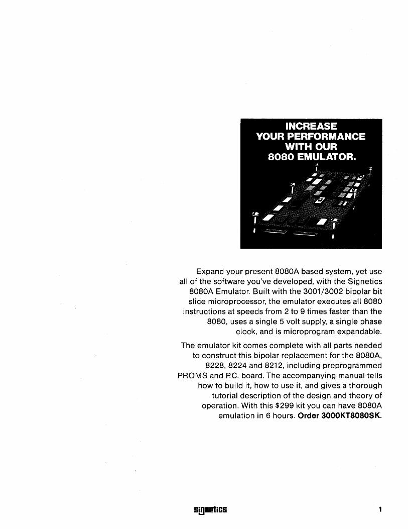
Expand your present 8080A based system, yet use all of the software you've developed, with the Signetics
8080A Emulator. Built with the 3001/3002 bipolar bit slice microprocessor, the emulator executes all 8080
instructions at speeds from 2 to 9 times faster than the 8080, uses a single 5 volt supply, a single phase
clock, and is microprogram expandable.
The emulator kit comes complete with all parts needed to construct this bipolar replacement for the 8080A,
8228, 8224 and 8212, including preprogrammed PROMS and p.e. board. The accompanying manual tells
how to build it, how to use it, and gives a thorough tutorial description of the design and theory of
operation. With this $299 kit you can have 8080A emulation in 6 hours. Order 3000KT8080SK.
!i!!lDOliC!i 1
Reach for this book anytime you need information on bipolar microprocessors. The following pages have everything here for quick easy reference to data sheets on:
• Bit Slice Microprocessor • Sequencers • M icrocontroller • Selected I nterface Products
with selection guides and summary data sheets for:
• Memory Products (including FPLA) • Analog Interface Products • Interface Circuits • System Logic
and references and data sheets on:
• Development Systems • Development Software
and data sheets on kits and appl ication notes. Yes, it's all here.
2 9i!1DOliC9
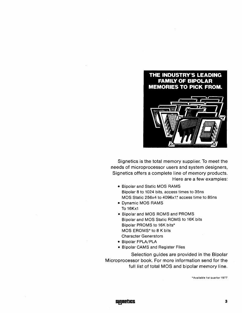
Signetics is the total memory supplier. To meet the needs of microprocessor users and system designers, Signetics offers a complete line of memory products.
Here are a few examples:
• Bipolar and Static MOS RAMS Bipolar 8 to 1024 bits, access times to 35ns MOS Static 256x4 to 4096x1~ access time to 85ns
• Dynamic MOS RAMS To 16Kx1
• Bipolar and MOS ROMS and PROMS Bipolar and MOS Static ROMS to 16K bits Bipolar PROMS to 16K bits* MOS EROMS* to 8 K bits Character Generators
• Bipolar FPLA/PLA • Bipolar CAMS and Register Files
Selection guides are provided in the Bipolar Microprocessor book. For more information send for the
full list of total MOS and bipolar memory line.
*Available 1st quarter 1977
!ii!lDOliC!i 3

Complete with the 8X300, clock crystal, 4 I/O ports, 256 bytes of working storage, 512 words of program storage, and P.C. board with wire wrap area, the kit is ready to be used as a basic starter system for your own controller design. There are 450 empty PROM locations that can be used to hold the program for your controller using this, the industry's first high speed (Schottky) complete 8-bit microprocessor. The remaining 62 locations contain diagnostics which can be used to check out the board or monitor the 8X300 through Single Step and_lnstructidn Jam features of this kit. This $299 kit is a fast, inexpensive way to get started with the 8X300. Order 8X300KT100SK.
4 !ii!lDOliCS
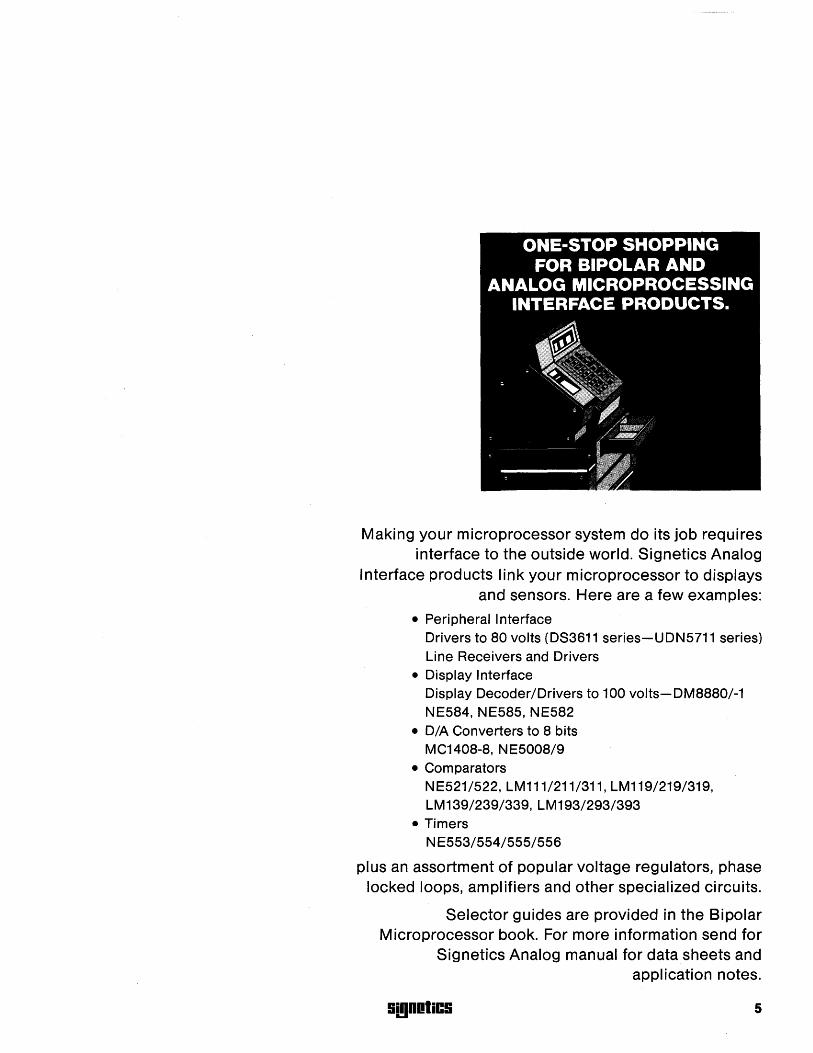
Making your microprocessor system do its job requires interface to the outside world. Signetics Analog
Interface products link your microprocessor to displays and sensors. Here are a few examples:
• Peripheral Interface Drivers to 80 volts (DS3611 series-UDN5711 series) Line Receivers and Drivers
• Display Interface Display Decoder/Drivers to 100 volts-DM8880/-1 NE584, NE585, NE582
• D/A Converters to 8 bits MC1408-8, NE5008/9
• Comparators NE521/522, LM111/211/311, LM119/219/319, LM139/239/339, LM193/293/393
• Timers N E553/554/555/556
plus an assortment of popular voltage regulators, phase locked loops, amplifiers and other specialized circuits.
Selector guides are provided in the Bipolar Microprocessor book. For more information send for
Signetics Analog manual for data sheets and appl ication notes.
!iI!lDOliC!i 5
An easy way to get a complete set of parts for a bit slice microprocessor is with this kit of parts. An 8-bit processor can be constructed using the four 3002's with microcontrol provided by the 3001 and two 828114's contained in the kit. In addition you get two 8T26A bus transceivers and an 8T31 bidirectional I/O ports to round out the parts complement. For your start in bit slice microprocessors, get this $230 value with data book for $100. Order 3000KT100SK.
6 9!!1DOIIC9
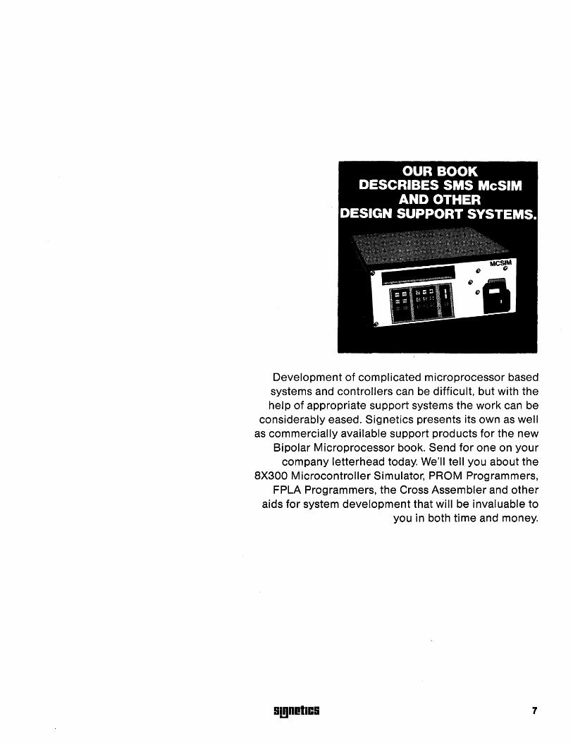
Development of complicated microprocessor based systems and controllers can be difficult, but with the help of appropriate support systems the work can be
considerably eased. Signetics presents its own as well as commercially available support products for the new
Bipolar Microprocessor book. Send for one on your company letterhead today. We'll tell you about the
8X300 Microcontroller Simulator, PROM Programmers, FPLA Programmers, the Cross Assembler and other
aids for system development that will be invaluable to you in both time and money.
9!!1DOliC9 7
Signetics "Answermen" are there to solve your problems not just sell you a microprocessor. Microprocessor Application Specialists, 9 in all, located in strategic parts of the country serve customers in all corners of the continental United States. Well versed in Signetics MOS, bipolar bit slice and bipolar microcontroller microprocessors through regular intensive factory training, these "Answermen" have no limit in technology they may draw upon to provide you with a cost effective approach to your task. They may suggest the 2650, the 3002, the 2901-1 or the 8X300 in combination with System Logic, Interface and support circuits in an architecture that can do the job with the least cost. And for more difficult problems, the "Answermen" may draw on the factory staff of application experts. Call an "Answerman" for a discussion of your specific needs or for a seminar on the Signetics product line. "Answermen" are located in:
Sunnyvale Boston Los Angeles Irvine New York Pompano Beach Minneapolis Philadelphia Dallas
8 9!!1DOliC9
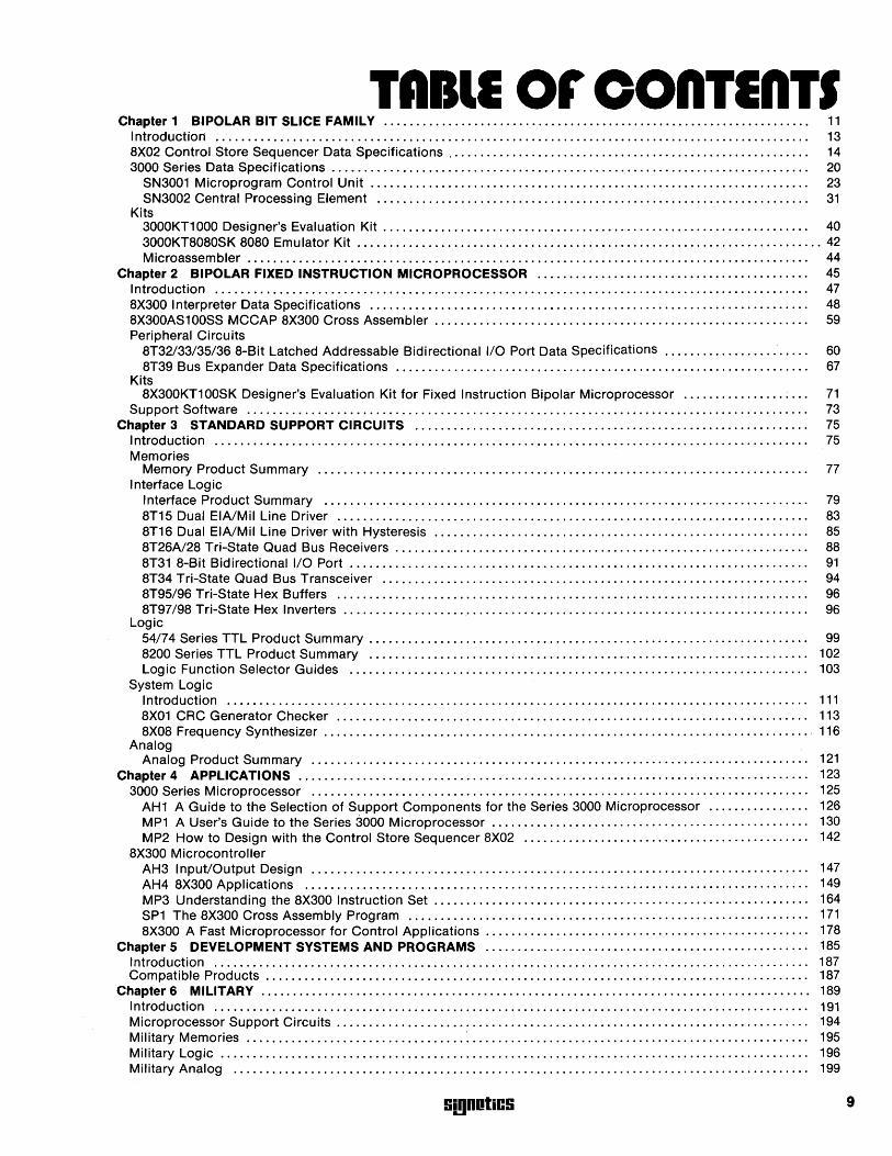
TAIII or conTlnTS Chapter 1 BIPOLAR BIT SLICE FAMILy................................................................... 11
Introduction ............................................................................................. 13 8X02 Control Store Sequencer Data Specifications..... . .. . . ... .. .. .. ..... ........ ........ ....... .... ...... 14 3000 Series Data Specifications ........................................................................... 20
SN3001 Microprogram Control Unit..................................................................... 23 SN3002 Central Processing Element .................................................................... 31
Kits 3000KT1000 Designer's Evaluation Kit................................................................... 40 3000KT8080SK 8080 Emulator Kit ......................................................................... 42 Microassembler ........................................................................................ 44
Chapter 2 BIPOLAR FIXED INSTRUCTION MICROPROCESSOR ........................................... 45 Introduction ............................................................................................. 47 8X300 I nterpreter Data Specifications ..................................................................... 48 8X300AS100SS MCCAP 8X300 Cross Assembler. . . . . . . . . . . . . . . . . . . . . . . . . . . . . . . . . . . . . . . . . . . . . . . . . . . . . . . . . . . 59 Peripheral Circuits
8T32/33/35/36 8-Bit Latched Addressable Bidirectional I/O Port Data Specifications ...................... . 60 8T39 Bus Expander Data Specifications ................................................................ . 67
Kits 8X300KT100SK Designer's Evaluation Kit for Fixed Instruction Bipolar Microprocessor ................... . 71
Support Software ....................................................................................... . 73 Chapter 3 STANDARD SUPPORT CIRCUITS ............................................................. . 75
Introduction ............................................................................................ . 75 Memories
Memory Product Summary ............................................................................ . 77 I nterface Log ic
Interface Product Summary ........................................................................... . 79 8T15 Dual EIA/Mil Line Driver ......................................................................... . 83 8T16 Dual EIA/Mil Line Driver with Hysteresis .......................................................... . 85 8T26A/28 Tri-State Quad Bus Receivers ................................................................ . 88 8T31 8-Bit Bidirectional I/O Port ....................................................................... . 91 8T34 Tri-State Quad Bus Transceiver .................................................................. . 94 8T95/96 Tri-State Hex Buffers ......................................................................... . 96 8T97/98 Tri-State Hex Inverters ........................................................................ . 96
Logic 54174 Series TTL Product Summary .................................................................... . 99 8200 Series TTL Product Summary .................................................................... . 102 Logic Function Selector Guides ....................................................................... . 103
System Logic Introduction .......................................................................................... . 111 8X01 CRC Generator Checker ......................................................................... . 113 8X08 Frequency Synthesizer ............ " ............................................................. . 116
Analog Analog Product Summary ............................................................................. . 121
Chapter 4 APPLICATIONS ............................................................................... . 123 3000 Series Microprocessor ............................................................................. . 125
AH1 A Guide to the Selection of Support Components for the Series 3000 Microprocessor ............... . 126 MP1 A User's Guide to the Series 3000 Microprocessor ...... '" ........................................ . 130 MP2 How to Design with the Control Store Sequencer 8X02 ............................................ . 142
8X300 Microcontroller AH3 Input/Output Design ............................................................................. . 147 AH4 8X300 Applications .............................................................................. . 149 MP3 Understanding the 8X300 Instruction Set .......................................................... . 164 SP1 The 8X300 Cross Assembly Program .............................................................. . 171 8X300 A Fast Microprocessor for Control Applications .................................................. . 178
Chapter 5 DEVELOPMENT SYSTEMS AND PROGRAMS .................................................. . 185 Introduction ............................................................................................ . 187 Compatible Products .................................................................................... . 187
Chapter 6 MILITARy ..................................................................................... . 189 Introduction ............................................................................................ . 191 Microprocessor Support Circuits ......................................................................... . 194 Military Memories .................................. ~ .................................................... . 195 Military LogiC ........................................................................................... . 196 Military Analog ......................................................................................... . 199
!i!!lDotiC!i 9

10 S!!)DotiCS
!i!!lDotiC!i
OIIAPTIR I IIPOIAR liT 11101 rAmiiT
11

12 9i!1DOliC9
BIT-SLICE MICROPROCESSOR SERIES
M icrocontrol and Arithmetic Units
The introduction of the Signetics Bit-Slice Microprocessors has brought new levels of high performance to microprocessor applications not previously possible with MOS technology. Combining the Schottky bipolar microprocessors with industry standard memory and support circuits, microinstruction cycle times of 100ns are possible.
In the majority of cases, the choice of a bipolar microprocessor slice, as opposed to an MOS device, is based on speed or flexibility of microprogramming. Starting with these characteristics, the design of the Signetics slice microprocessors has been optimized around the following objectives:
• Fast cycle time • All memory and support chips are industry
standard • Cooler operation • Lower total system cost
Furthermore, systems built with large-scale integrated circuits are much smaller and require less power than equivalent systems using medium andlor small scale integrated circuits.
Typically, slice microprocessors are employed in the realization of the Central Processing Unit (CPU) of a computer or for implementing dedicated smart controllers. The generalized and simplified structure of a CPU or "Smart" controller can be typically classified into 3 distinct but interactively related functional sections. These sections are generally referred to as the Processing section, the Control section, and the liD and Memory Interface section. A simplified block diagram of a CPU is illustrated in Figure 1.
The major functions of the Processing section are to:
• provide data transfer paths; • manipulate data through logic and arithmetic
operations; • provide storage facilities such as a register file;
and • generate necessary status flags based on the
kind of operation performed by the ALU.
A SIMPLIFIED CPU ORGANIZATION
CONTROL oJ PROCESSING SECTION SECTION
~ * I 1/0 AND MEMORY INTERFACE 1
Figure 1
The major functions of the Control section are to:
• initiate memory or I/O operations; • decode macroinstructions; • control the manipulation and transfer of data; • test status conditions; and • sample and respond to interrupts.
The major functions of the liD and Memory Interface section are to:
• multiplex data to the proper destination; • provide bus driving/receiving capability; and • provide latching capability.
With state-of-the-art bipolar Schottky technology, high-performance microprocessors are designed to perform functions of the Processing section. Due to the limitation on the number of pins and chip size, the overall Processing section is partitioned into several functionally equivalent slices. In today's bipolar microprocessor market, 2-bit and 4-bit slice architecture predominates. Each architecture type has its uniqueness but, in general, a slice contains a group of general purpose registers, an accumulator, special
needed to implement the microprogram sequencing can now be replaced by the Microprogram Control Unit; and, of course, the microprogram can be stored in high density PROMs or ROMs. Since the designer must define his own microstructure, the slice microprocessors permit fundamental optimizations to be made. With slice hardware, the designer may have no macroinstructions at all, placing all of the program in PROM for dedicated control applications. Or he may define, as required, any number of macroinstructions selected specifically for his particular processor purpose. Various minicomputers and several MOS microprocessors have been emulated using slice hardware.
The liD and Memory I nterface section consists mainly of I/O ports, high power bus drivers, receivers, and some temporary register storage facilities. Bidirectional and tri-state devices are the most popular logic elements for implementing this interface structure.
purp,ose register(s) ALU and related status Figure 2 shows an LSI approach to the flags. All of these elements constitute the implementation of the same generalized Processing section of a CPU. The flexibility CPU structure indicated earlier. of slice components allows the designer to construct a processing section of any de- The devices presented in this chapter rep-sired width as required by his application. resent Signetics line of slice microproc-
essor components. Included is the popular The Control section of the CPU is more 3000 series Microprogram Control Unit and complex in design. Typically this section the 2-bit slice Central Processing Element. includes the macroinstruction decode log- These Signetics devices feature improved ic, test-branch decode, microprogram se- performance specifications over 3000 series quencing logic, and the control store where components available on the general marthe microprogram resides. Aside from the ket. Moreover, the unique Signetics XL plasmicroprogram, the remaining portion of the tic package design results in significantly Control section (macroinstruction decode cooler operation of the chip than was previand test-branch decode and sequencing ously possible with other plastic package logic), does not lend itself to efficient parti- designs. This section also features the 8X02 tioning into vertical slices. This is due to the Control Store Sequencer. This device may random nature of the logic usually found in be used with any TTL compatible slice the Control section. However, horizontal processing elements and features extreme functional grouping is possible. For exam- ease of use. The 8 simple, yet powerful, pie, the macroinstruction decode and test- instructions permit subroutining and loop-branch decode logic can now be replaced ing (using internal stack), unrestricted by the FPLA (Field Programmable Logic jumping, unrestricted conditional branch-Array); the random logic traditionally ing and conditional instruction skipping.
AN LSI IMPLEMENTATION OF A CPU CONTROL SECTION
ROM-PROM PROCESSING SECTION (MICROPROGRAM) "'f)
82S115 \.\.
~ 1st SLICE 2nd SLICE nth SLICE
MCU (SEQUENCER) ~ N3002 N3002 N3002 N3001 OR 8X02 OR OR OR
N2901-1 N2901-1 N2901-1
FPLA (FOR DECODE) _:n 82S100/101 \.c
~. 1
1/0 AND MEMORY INTERFACE SECTION
8T31 - 8-BIT 1/0 PORT 8T28/8T26A - 4-BIT HIGH DRIVE TRANSCEIVER 8T95 - 98; HEX TRI-STATE BUFFERS
Figure 2
!i!!lDotiC!i 13
tOIlIIOt SIORE SEQ"EUCER 8A" OBJECTIVE SPECIFICATION 8X02-Xl,1
DESCRIPTION FEATURES PIN CONFIGURATION The Signetics 8X02 is a low-Power Schottky lSI device intended for use in high performance microprogrammed systems to control the fetch sequence of microinstructions. When combined with standard ROM or PROM, the 8X02 forms a powerful microprogrammed control section for computers, controllers, or sequenced logic.
• Low power Schottky process • 77ns cycle time (typ) • 1024 microinstruction addressability • N-way branch • 4-level stack register file (LIFO type) • Automatic push/pop stack operation • "Test & skip" operation on test input line • 3-bit command code
BLOCK DIAGRAM
(2)
(1) AC2 (2S) AC1
(27) ACO (25) ClK o--J (22) VCC~
(7) GND0--4
I
PIN DESCRIPTION
PIN SYMBOL
5-6 Ao-Ag 8-13
1,28,27 ACo-AC2
14-21 Bo-Bg
• Tri-state buffered outputs • Auto-reset to address 0 during power-up • Conditional branching, pop stack, &
push stack
(12) (10) (S) (5) (3) (13) (11) (g) (S) (4)
AgASA7ASA5A4A3A2A1AO
---------------, ~~~~-L~~~~ 10
t-o TEST I (2S)
I • I _____________ .-J
Bg BS B7 Bs B5 B4 B3 B2 B1 BO (24) (21) (19) (17) (15)
(23) (20) (lS) (lS) (14)
NAME AND FUNCTION
Microprogram Address outputs
Next Address Control Function inputs All addressing control functions are selected by these command lines.
Branch Address inputs
I.XL PACKAGE
TYPE
Th ree-state Active high
Active high
Active high 23-24 Determines the next address of an N-way branch when used with the BRANCH
TO SUBROUTINE (BSR) or BRANCH ON TEST (BRT) command.
2 EN Enable input Active low When in the low state, the Microprogram Address outputs are enabled.
25 ClK Clock input
All registers are triggered on the low-to-high transition of the clock. 26 TEST Test input Active high
Used in conjunction with four NEXT ADDRESS CONTROL FUNCTION commands to effect conditional skips, branches, and stack operations.
7 GND Ground
22 VCC +5 Volt supply
14 !ii!]DotiC!i
CONTROL STORE SEQUENCER
OBJECTIVE SPECIFICATION
FUNCTIONAL DESCRIPTION The Signetics 8X02 Control Store Sequencer is an LSI device using Low Power Schottky technology and is intended for use in high performance microprogrammed applications. When used alone, the 8X02 is capable of addressing up to 1 K words of microprogram. This may be expanded to any microprogram size by conventional paging techniques.
The Address Register consists of 10 D-type, edge-triggered flip-flops with a common clock. A new address is entered into the Address Register on the low-to-high transition of the clock. The next address to be entered into the Address Register is supplied via the Address Multiplexer.
The Address Multiplexer is a 5-input device that is used to select either the branch in put, +1 adder, +2 adder, stack register file, or ground (all zeros) as the source of the next microinstruction address. The proper multiplexer channel is automatically selected via the Decode Logic according to the Address Control Function Input and Test Input line.
The +1, +2 logic is used to increment the present contents of the Address Register by 1 or 2, depending on the function input command. Thus, the next address to the
Control Store ROM/PROM may be either the current address plus 1 (N+1) or the current address plus 2 (N+2). If the same Microprogram Address is to be used on successive occasions, the clock to the 8X02 must simply be disabled; therefore, no new address is loaded into the Address Register.
The Stack File Register is used to provide a return address linkage whenever a subroutine or loop is executed. The 4X10 stack operates in a last-in, first-out (LIFO) mode, with the stack pointer always pointing to the next address to be read. Operation of the stack pointer is automatically controlled by the Address Control Function Inputs. Since the stack is 4 words deep, up to 4 loops and/or subroutines may be nested.
The branch input is a 10-bit field of direct inputs to the multiplexer which can be selected as the next control store address. USing the appropriate branch command, an N-way branch is possible where N is the address of any microinstruction within the 1024 word microcode page. Likewise, the RESET command is a special case of an Nway branch in which the multiplexerselects an all zeros input, forcing the next microinstruction address to be zero.
NEXT ADDRESS CONTROL FUNCTION
MNEMONIC
TSK
INC
BLT
POP
BSR
PLP
BRT
RST
X Don t care N.C. = No change
DESCRIPTION
Test & skip
Increment
Branch to loop if test input true
POP stack
Branch to sub-routine if test input true
Push for looping
Branch if test input true
Set microprogram address output to zero
FUNCTION AC2 1 0
TEST NEXT ADDRESS
000 False Current + 1 True Current + 2
o 0 1 X Current + 1
o 1 0 False Current + 1 True Stack reg fi Ie
o 1 1 X Stack reg file
100 False Current + 1 True Branch address
1 o 1 X Current + 1
1 1 0 False Current + 1 True Branch address
1 1 1 X All O's
!ii!)Dl!tiC!i
8102 8X02-XL,1
The Test Input line is used in conjunction with the conditional execution of 4 Address Control Function commands. When the Test Input is false (low), the sequencer simply increments to the next address (N+1). When it is true (high), the sequencer executes a branch as defined by the input command, thereby transferring control to another portion of the microprogram.
All Address Output lines of the 8X02 are three-state buffered outputs with a common enable line (EN). When the Enable line is high, all outputs are placed in a highimpedance state, and external access to the control store ROM/PROM is possible. This allows a preprogrammed set of microinstructions to be executed from external or built-in test equipment (BITE), vectored interrupts, and Writable Control Store if implemented.
STACK STACK POINTER
N.C. N.C. N.C. N.C.
N.C. N.C.
X Decr POP (read) Decr
POP (read) Decr
N.C. N.C. PUSH (Curr + 1) Incr
PUSH (Curr Addr) Incr
N.C. N.C. N.C. N.C.
N.C. N.C.
15
CONTROL STOkE SEQUEI.tEk
OBJECTIVE SPECIFICATION
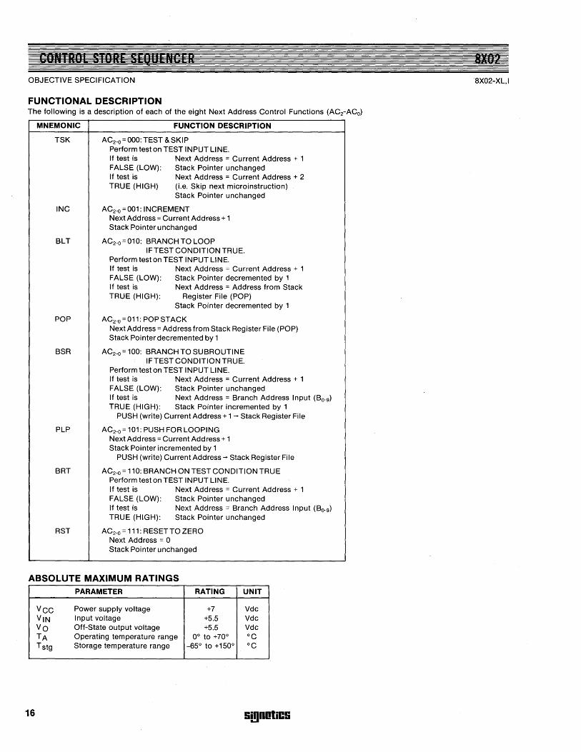
FUNCTIONAL DESCRIPTION The following is a description of each of the eight Next Address Control Functions (AC2-ACo)
MNEMONIC
TSK
FUNCTION DESCRIPTION
AC2-o = 000: TEST & SKI P Perform test on TEST INPUT LINE. If test is FALSE (LOW): If test is TRUE (HIGH)
Next Address = Current Address + 1 Stack Pointer unchanged Next Address = Current Address + 2 (i.e. Skip next microinstruction) Stack Pointer unchanged
INC AC2-o = 001: INCREMENT Next Address = Current Address + 1 Stack Pointer unchanged
BL T AC2-o = 010: BRANCH TO LOOP IFTEST CONDITION TRUE.
Perform test on TEST INPUT LINE. If test is FALSE (LOW): If test is TRUE (HIGH):
Next Address = Current Address + 1 Stack Pointer decremented by 1 Next Address = Address from Stack
Register File (POP) Stack Pointer decremented by 1
POP AC2-0 = 011: POP STACK Next Address = Address from Stack Register File (POP) Stack Pointer decremented by 1
BSR AC2-o = 100: BRANCH TO SUBROUTINE IFTEST CONDITION TRUE.
Perform test on TEST I N PUT LI N E. If test is Next Address = Current Address + 1 FALSE (LOW): Stack Pointer unchanged If test is Next Address = Branch Address Input (Bo-g) TRUE (HIGH): Stack Pointer incremented by 1
PUSH (write) Current Address + 1 --+ Stack Register File
PLP AC2-o = 101: PUSH FOR LOOPING Next Address = Current Address + 1 Stack Pointer incremented by 1
PUSH (write) Current Address --+ Stack Register File
BRT AC2-o = 110: BRANCH ON TEST CONDITION TRUE Perform test on TEST I N PUT LI N E. If test is FALSE (LOW): If test is TRUE (HIGH):
Next Address = Current Address + 1 Stack Pointer unchanged Next Address = Branch Address Input (Bo-g) Stack Pointer unchanged
RST AC2-0 = 111: RESET TO ZERO Next Address = 0 Stack Pointer unchanged
ABSOLUTE MAXIMUM RATINGS PARAMETER RATING UNIT
VCC Power supply voltage +7 Vdc VIN Input voltage +5.5 Vdc Vo Off-State output voltage +5.5 Vdc TA Operating temperature range 0° to +70° °c T stg Storage temperature range -65° to +150° °c
16 !ii!l0otiC!i
0)(112
8X02-XL,1
CaNTle' STORr Sre"L JCLR 8](02
OBJECTIVE SPECIFICATION SX02-XL,1
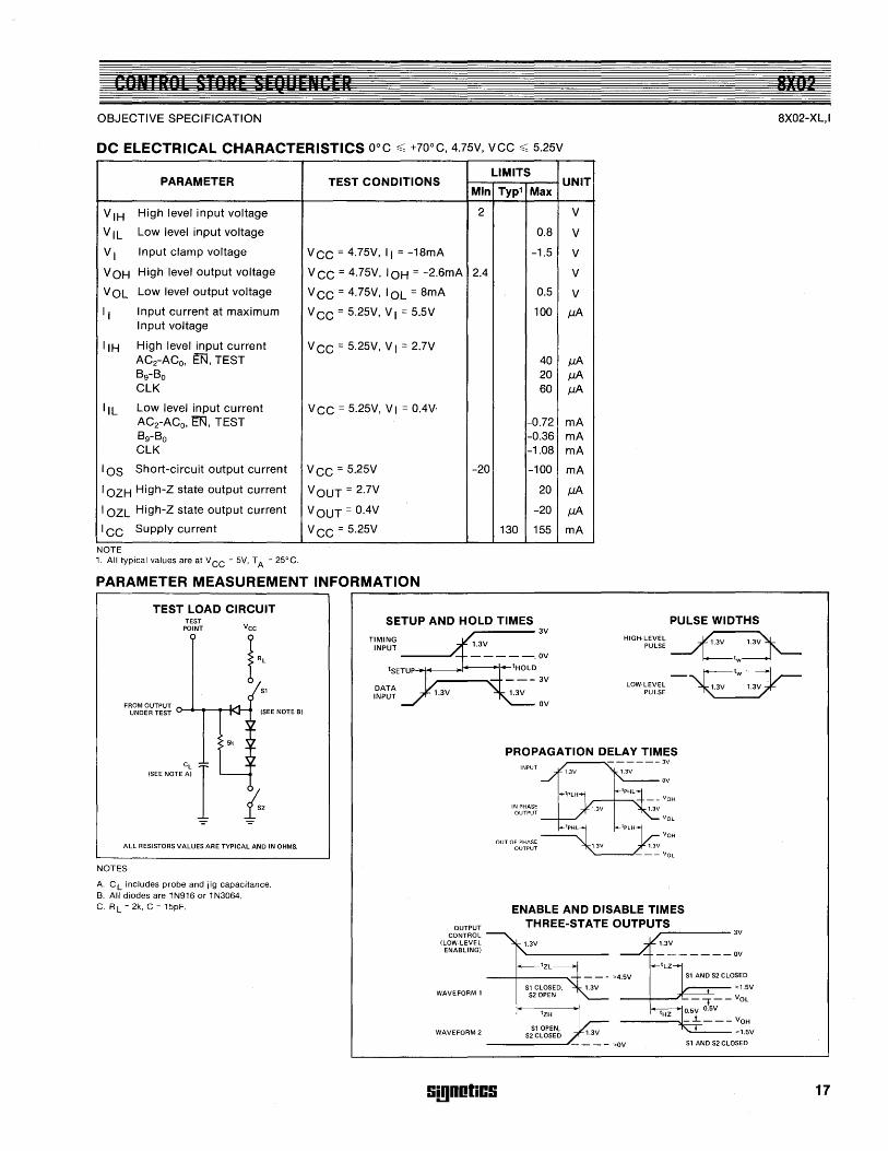
DC ELECTRICAL CHARACTERISTICS O°C ~ +70°C, 4.7SV, VCC ~ S.2SV
LIMITS PARAMETER TEST CONDITIONS UNIT
Min Typ1 Max
V IH High level input voltage 2 V
VIL Low level input voltage O.S V
VI Input clamp voltage V CC = 4.7SV, II = -1SmA -1.5 V
VOH High level output voltage VCC = 4.7SV, 10H = -2.6mA 2.4 V
VOL Low level output voltage V CC = 4.7SV, 10L = SmA 0.5 V
II Input current at maximum V CC = S.2SV, V I = S.SV 100 J.1A Input voltage
IIH High level input current V CC = S.2SV, V I = 2.7V AC2-ACo, EN, TEST 40 J.1A B9-Bo 20 J.1A CLK 60 J.1A
IlL Low level input current V CC = S.2SV, V I = O.4V, AC2-ACo, EN, TEST -0.72 mA B9-Bo -0.36 mA CLK -1.0S mA
lOS Short-circuit output current VCC = S.2SV -20 -100 mA
10ZH High-Z state output current VOUT = 2.7V 20 J.1A 10ZL High-Z state output current VOUT = O.4V -20 J.1A ICC Supply current V CC = S.2SV 130 155 mA
NOTE 1. All typical values are at V cc = 5V, T A = 25° C.
PARAMETER MEASUREMENT INFORMATION
TEST LOAD CIRCUIT TEST
POINT
S1
F~~~~~~~~icr-'"'- .......... __ }K~J--. (SEE NOTE B)
~~ 5k ... 7 ...
~~ --
ALL RESISTORS VALUES ARE TYPICAL AND IN OHMS.
NOTES
A. C L includes probe and jig capacitance. B. All diodes are 1 N916 or 1 N3064. C. RL = 2k, C = 15pF.
SETUP AND HOLD TIMES PULSE WIDTHS
TIMING INPUT
DATA INPUT
,._----3V HIGH·LEVEL ~3V 13V
PULSE . .
'w
~w
LOW-LEVEL 1.3V 1.3V PULSE
ov
PROPAGATION DELAY TIMES INPUT
IN PHASE OUTPUT
VOH ~PHL tpLH
OUT OF PHASE 1 3V 1 3V OUTPUT . .
OUTPUT CONTROL
(LOW-LEVEL ENABLING)
WAVEFORM 1
WAVEFORM 2
Si!lDotiCS
--- VOL
ENABLE AND DISABLE TIMES THREE-STATE OUTPUTS
~----3V
'ZH
S10PEN, S2 CLOSED ~--"'1.5V
S1 AND S2 CLOSED
17
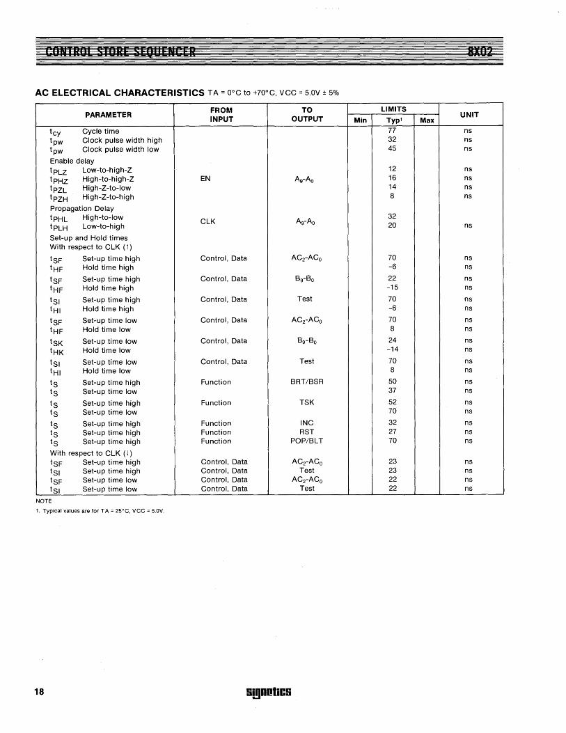
AC ELECTRICAL CHARACTERISTICS TA = O°C to +70°C, VCC = 5.0V ± 5%
PARAMETER FROM TO LIMITS INPUT OUTPUT
UNIT Min Typ1 Max
tcy Cycle time 77 ns
tpw Clock pulse width high 32 ns
tpw Clock pulse width low 45 ns
Enable delay
tplZ low-to-high-Z 12 ns
tpHZ High-to-high-Z EN A9-AO 16 ns
tpZl High-Z-to-Iow 14 ns
tpZH High-Z-to-high 8 ns
Propagation Delay
tpHl High-to-Iow ClK A9-AO
32
tplH low-to-high 20 ns
Set-up and Hold times With respect to ClK (1)
tSF Set-up time high Control, Data AC2-ACo 70 ns
tHF Hold time high -6 ns
tSF Set-up time high Control, Data B9-BO 22 ns
tHF Hold time high -15 ns
tSI Set-up time high Control, Data Test 70 ns
tHI Hold time high -6 ns
tSF Set-up time low Control, Data AC2-ACo 70 ns
tHF Hold time low 8 ns
tSK Set-up time low Control, Data B9-Bo 24 ns
tHK Hold time low -14 ns
tSI Set-up time low Control, Data Test 70 ns
tHI Hold time low 8 ns
ts Set-up time high Function BRT/BSR 50 ns
ts Set-up time low 37 ns
ts Set-up time high Function TSK 52 ns
ts Set-up time low 70 ns
ts Set-up time high Function INC 32 ns
ts Set-up time high Function RST 27 ns
ts Set-up time high Function POP/BlT 70 ns
With respect to ClK (j)
tSF Set-up time high Control, Data AC2-ACo 23 ns
tSI Set-up time high Control, Data Test 23 ns
tSF Set-up time low Control, Data AC2-ACo 22 ns
tSI Set-up time low Control, Data Test 22 ns
NOTE
1. Typical values are for T A = 25°e. vee = 5.0V.
18 S!!)DotiCS
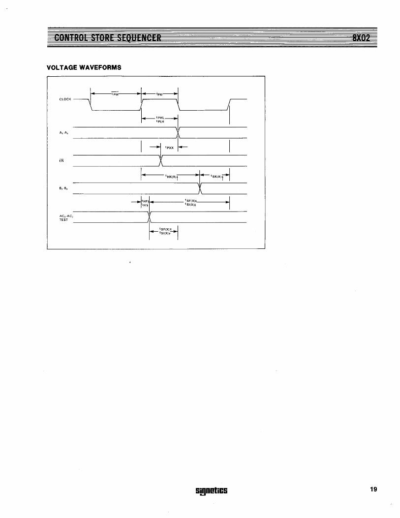
CONTROl STORE SEQUE'ICER
VOLTAGE WAVEFORMS
,w" --i ~w-i --.'W=1L---.------1AI I-:;~~=j.-------
AoA, )(
I =J "" r= rn ----------------- X~ ________________ _
1··- tHK1X)-t ----.-I1--.. -tSKIX)r1
~I ---ltHF.~ tSFIX)+ .. ~ltHI.I,---- tSllXH
ACo·AC,-----------v; -------------
TEST A
F:~~~lt~
Si!lDotiCS
8X'"
19
DIPOLAR MICROPkOCESS"R
INTRODUCTION The introduction of the Signetics Series 3000 Bipolar Microprocessor Chip Set has brought new levels of high performance to microprocessor applications not previously possible with MaS technology. Combining the Schottky bipolar N3001 Microprogram Control Unit (MCU) and N3002 Central Processing Element (CPE) with industry standard memory and support circuits, microinstruction cycle times of 100ns are possible.
In the majority of cases, the choice of a bipolar microprocessor slice, as opposed to an MaS device, is based on speed or flexibility of microprogramming. Starting with these characteristics, the design of the Signetics Series 3000 Microprocessor has been optimized around the following objectives:
• Fast cycle time • All memory and support chips are industry
standard • Cooler operation • Lower total system cost
Furthermore, systems built with large-scale integrated circuits are much smaller and require less power than equivalent systems using medium and/or small scale integrated circuits.
The 2 components of the Series 3000 chip set, when combined with industry standard memory and peripheral circuits, allows the design engineer to construct highperformance processors and/or controllers
20
I/O CONTROL
MICRO PROGRAM MEMORY (82S115)
with a minimum amount of auxiliary logic. Features such as the multiple independent address and data buses, tri-state logic, and separate output enable lines eliminate the need for time-multiplexing of buses and associated hardware.
Each Central Processing Element represents a complete 2-bit slice through the data processing section of a computer. Several CPEs may be connected in parallel to form a processor of any desired word length. The Microprogram Control Unit controls the sequence in which microinstructions are fetched from the microprogram memory (ROM/PROM), with these microinstructions controlling the step-by-step operation of the processor.
Each CPE contains a 2-bit slice of 5 independent buses. Although they can be used in a variety of ways, typical connections are:
Input M-bus: Carries data from external memory
Input .I-bus: Carries data from input/output device
Input K-bus: Used for microprogram mask or literal (constant) value input
Output A-bus: Connected to CPE Memory Address Register
Output D-bus: Connected to CPE accumulator.
As the CPEs are paralleled together, all buses, data paths, and registers are correspondingly expanded.
The microfunction input bus (F-bus) con-
MICROCOMPUTER BLOCK DIAGRAM
SF illES 100
trois the internal operation of the CPE, selecting both the operands and the operation to be executed upon them. The arithmetic logic unit (ALU), controlled by the microfunction decoder, is capable of over 40 Boolean and binary operations as outlined in the Function Description section of the N3002 data sheet. Standard carry look-ahead outputs (X and Y) are generated by the CPE for use with industry standard devices such as the 74S182.
A typical processor configuration is shown in Figure 1. It should be remembered that in working with slice-oriented microprocessors, the final configuration may be varied to enhance speed, reduce component count, or increase data-processing capability. One method of maximizing a processor's performance is called pipelining. To accomplish this, a group of D-type flip-flops or latches (such as the 74174 Hex D-type Flip-Flop) are connected to the microprogram memory outputs (excluding the address control field ACo-AC6) to buffer the current microinstruction and allow the MCU to overlap the fetch of the next instruction with the execution of the current one. The time saved in pipelining operations is the shorter of either the address set-up time to the microprogram memory (ROM/PROM) or the access time of the ROM/PROM. A convenient way of implementing pipelining is to use ROMs with on-board latches, such as the Signetics 82S115.
MEMORY ADDRESS BUS DATA BUS
FROM I/O DEVICES DATA IN FROM MEMORY
Figure 1
Si!)DotiCS
*Carry-in of first stage "Carry-out of last stage
BI fBLAR MICRBP RBCESSBR
Figure 2 shows a typical microinstruction format using the 82S114 PROMs contained in the Signetics 3000 Microprocessor Designer's Evaluation Kit. Although this particular example is for a 48-bit word (6 PROMs), the allocation of bits for the mask (K-bus) and optional processor functions depends on the specific application of the system and the trade offs which the designer wishes to make.
In using the K-bus, it should be kept in mind that the K inputs are always ANDed with the B-multiplexer outputs into the ALU. Bit masking, frequently done in computer control systems, can be performed with the mask su ppl ied to the K-bus directly from the microinstruction.
By plaCing the K-bus in either the all-one or all-zero condition (done with a single control bit in the microinstruction), the accumulator will either be selected or deselected, respectively, in a given operation. This feature nearly doubles the amount of microfunctions in the CPE. A description of these various microfunctions can be found in the N3002 data sheet under the heading Function Description by referring to the Kbus conditions of all-ones (11) and all-zeros (00).
The MCU controls the sequence in which microinstructions are fetched from the mi-
croprogram memory (ROM/PROM). In its classical form, the MCU would use a nextaddress field in each microinstruction. However, the N3001 uses a modified classical approach in which the microinstruction field specifies conditional tests on the MCU bus inputs and registers. The next-address logic of the MCU also makes extensive use of a row/column addressing scheme, whereby the next address is defined by a 5-bit row address and 4-bit column address. Thus, from a particular address location, it is possible to jump unconditionally to any location within that row or column, or conditionally to other specified locations in one operation. Using this method, the processor functions can be executed in parallel with program branches.
As an example of this flexibility, let us assume a disk controller is being deSigned. As part of the sequence logic, 3 bits of the disk drive status word must be tested and all 3 must be true in order to proceed with the particular sequencing operation. In any sequencing operation using a status word for conditional branch information, there are innumerable combinations of bits which must be tested throughout the sequencing operation. Using discrete logic techniques, this would involve several levels of gating.
However, the entire operation can be done in two microinstructions. First, the mask (K-
TYPICAL MICROINSTRUCTION FORMAT
SERIES JOIiO
bus) field in the microinstruction format is encoded with a one for each corresponding status bit to be tested and a zero for each bit to be discarded. The status word is input via the I-bus and ANDed with the K-bus mask using the CPE microfunction operation from F-Group 2, R-Group III. Assuming we are using low-true logic (true = 0 volts), we now test the result, which is located in the accumulator AC, for all zeros using the CPE microfunction operation from F-Group 5, R-Group III. Depending on the zero/nonzero status of AC, a one or zero will be loaded into the carryout CO bit. This bit can now be used as a condition for the next address jump calculation within the N3001 MCU. If the AC was zero (status word was true), we will jump to the next address within our controller sequence. If the AC was nonzero (status word not true), then a jump would be made back to the beginning of this 2-microinstruction loop and the test sequence repeated until the status word (all 3 bits) is true.
Figure 3 shows a typical timing diagram for a system operating in the non-pipelined mode. Keep in mind that the maximum clock rate is dependent upon the total of propagation delay times plus required setup times. It is at the designer's discretion to resolve the speed versus complexity tradeofts.
USER·DEFINABLE FUNCTION FIELDS STANDARD FUNCTION FIELDS
~------------------~------------------- ---------~------------r ~,
47 44143 40139 36135 32131 28127 24123
USER DEFINED MASK OR OPTIONAL
FUNCTIONS PROCESSOR FUNCTIONS
Note: The mask field need only be used during masking operations. At other times, it is entirely user definable. Figure 2
20119 16115 12111 817 4 3 0
C.P.E. JUMP FLAG
FUNCTION FUNCTION LOGIC
(FO·F6) (ACO·AC6) FUNCTION
(FCO· FC3)
____________ ........ ---_V""_---1 TO N3002 TO N3001
SYSTEM TIMING-NON-PIPELINED CONFIGURATION
-I 36n51-MICROPROGRAM X X x= MEMORY AOOR
(MAO-8) I ~50n~ ~8n.51 ROM X X OUTPUT
N3002 ~ 40n5 r--OATAOUT X X x:::
(O-BUS)
Figure 3
!i!!lDotiC!i 21
al r UI AR "ICRI F R 1(:[ S iUR F RUDin,! I N FuRIA' Il,N
ABSOLUTE MAXIMUM RATINGS*
N3001/N3002 53001/53002
Temperature under bias ooe to +70 0 e -55° e to +125° e Storage temperature -60° e to +160° e -65°e to +150 0 e All output and supply voltages -0.5V to +7V -0.5V to +7V All input voltages -1.0V to +5.5V -1.0V to +5.5V Output currents 100mA 100mA
'Stresses above those listed under "Absolute Maximum Ratings" may cause permanent damage to the device. This is a stress rating only and functional operation of the device at these or any other conditions above those indicated in the operational sections of the specification is not implied. Exposure to absolute maximum ratings for extended periods may effect device reliability.
N3001/N3002 T A = 0° e to +70° e
DC ELECTRICAL CHARACTERISTICS S3001/S3002 T A = -55°e to +125°C
SEE'FS 1 a
PARAMETE.R MEASUREMENT INFORMATION
500
OUT u-~t----4
lk
NOTE: All resistor values are typical and in ohms. TEST CONDITIONS: Input pulse amplitude of 2.5 volts Input rise and fall times of 5ns between 1 volt and 2 volts Output load of 1 OmA and 50pF Speed measurements are taken at the 1.5 volt level
N3001/N3002 53001/53002 PARAMETER TEST CONDITIONS
Vil low level input voltage Vee = 5.OV VIH High level input voltage Vee = 5.OV
Vie Input clamp voitage Vee = 4.75V, Ie = -SmA
Val low level output voltage Vee = 4.75V, I Ol =10mA
VOH High level output voltage Vee = 4.75V, 10H = -1mA mAo - mAs, I SE, Fa
IF Input load current N3001 Vee = 5.25V, VF = 0.45V elK input EN input
All other inputs
IR Input leakage current N3001 Vee = 5.25V, VR = 5.25V elK input EN input
All other inputs
lOS Short circuit output current Vee = 5.OV mAo - mAs, ISE, Fa
10 Off-state output current Vee = 5.25V (off) PRo - PR2, mAo - mA2' Fa
VOUT = 0.45V mAo - mAs, Fa
J VOUT = 5.25V
lee Power supply current N3001 Vee = 5.25V2
Power supply current N3002
IF Input load eurrent N3002 Vee = 5.25V, V F = 0.45v
Fo-F6 , elK, Ko, K1, EA, ED 1o, 11, Mo, M1 , LI
el
IR Input leakage Current N3002 Vee = 5.25V, V R = 5.25V Fo-F6 , elK, Ko, K1 , EA, ED
10, 11 , Mo, M1 , LI el
NOTES 1. SN3001 typical values are for T A = 25° e, Vee = 5.0V 2. SN3002 EN input grounded, all other inputs and outputs open. SN3002 elK input grounded, other inputs open.
22 S!!IDotiCS
Min Typ
2.0 -0.55
0.35 2.4
-0.21 -0.12 -0.05
-15 -28
170
145
-0.05 -0.85 -2.3
UNIT Max Min Typ Max
0.8 0.8 V 2.0 V
-1.0 -0.8 -1.2 V
0.45 0.35 0.45 V
3.0 2.4 3.0 V
-0.75 -0.21 -0.75 mA -0.50 -0.12 -0.50 mA -0.25 -0.05 -0.25 mA
VR = 5.5V 120 120 J.1A 80 80 J.1A 40 40 J.1A
-60 -15 -28 -60 mA
-100 -100 J.1A VIoUT = 5.5V
+100 +100 J.1A
240 170 250 mA
190 145 210
-0.25 -0.05 -0.25 mA -1.5 -0.85 -1.5 mA -4.0 -2.3 -4.0 mA
40 40 J.1A 60 60 J.1A 180 180 J.1A
MICROPROGRAM CON 1IIlib ONII S N 30111
DESCRIPTION The N3001 MCU is 1 element of a bipolar microcomputer set. When used with the S/N3002, 54/74S182, ROM or PROM memory, a powerful microprogrammed computer can be implemented.
The 3001 MCU controls the fetch sequence of microinstructions from the microprogram memory. Functions performed by the 3001 include:
• Maintenance of microprogram address register • Selection of next microinstruction address • Decoding and testing of data supplied via
several input buses • Saving and testing of carry output data from the
central processing (CP) array • Control of carry/shift input data to the CP array • Control of microprogram interrupts
BLOCK DIAGRAM
ERA
EN
FCO
FC1
FC2
FC3
lD
ClK
Vcc
GND
ACO
AC1
AC2
AC3
AC4
AC5
AC6
,... ~
~
,... ~
,.."
,... ~
,.." ~
,.." -~
C>----<
C>----<
C>----<
,... ~
,.."
,... ~
,... ~
-,...
FO (
(
l
FLAG CONTROL H
F LATCH
!
t
FEATURES • Schottky TTL process • 45ns cycle time (typ.) • Direct addressing of standard bipolar
PROM or ROM • 512 microinstruction addressability • Advanced organization:
• 9-bit microprogram address register and bus organized to address memory by row and column
• 4-bit program latch • 2-flag registers
• 11 address control functions: • 3 jump and test latch function • 16 way jump and test instruction
• 8 flag control functions: • 4 flag input functions • 4 flag output functions
PIN CONFIGURATION
I PACKAGE
MA8 MAl MA6 MA5 MA4 MA3 MA2 MA 1 MAO
~ ) ( <) () ) ( > (
ROW I COLUMN 1 OUTPUT OUTPUT
1
h c, z FLAGS
I--i ADDRESS REGISTER
~ I J 9
I NEXT ADDRESS CONTROL
~~~ PR lATCH 3 OUT
-
( ~ ~ ( ~ ) ~ ~
o~~~ ~~~~ PXl PX6 PX5 PX4 SX3 SX2 SX1 SXO
!ii!ln~tiC!i
N3001-1
- ISE
,.. PRO
,... ~ PR1
~ PR2
23
M" "Q I'lt U G Ii n.. " PI T R " lUll T S N 11111
N3001-1
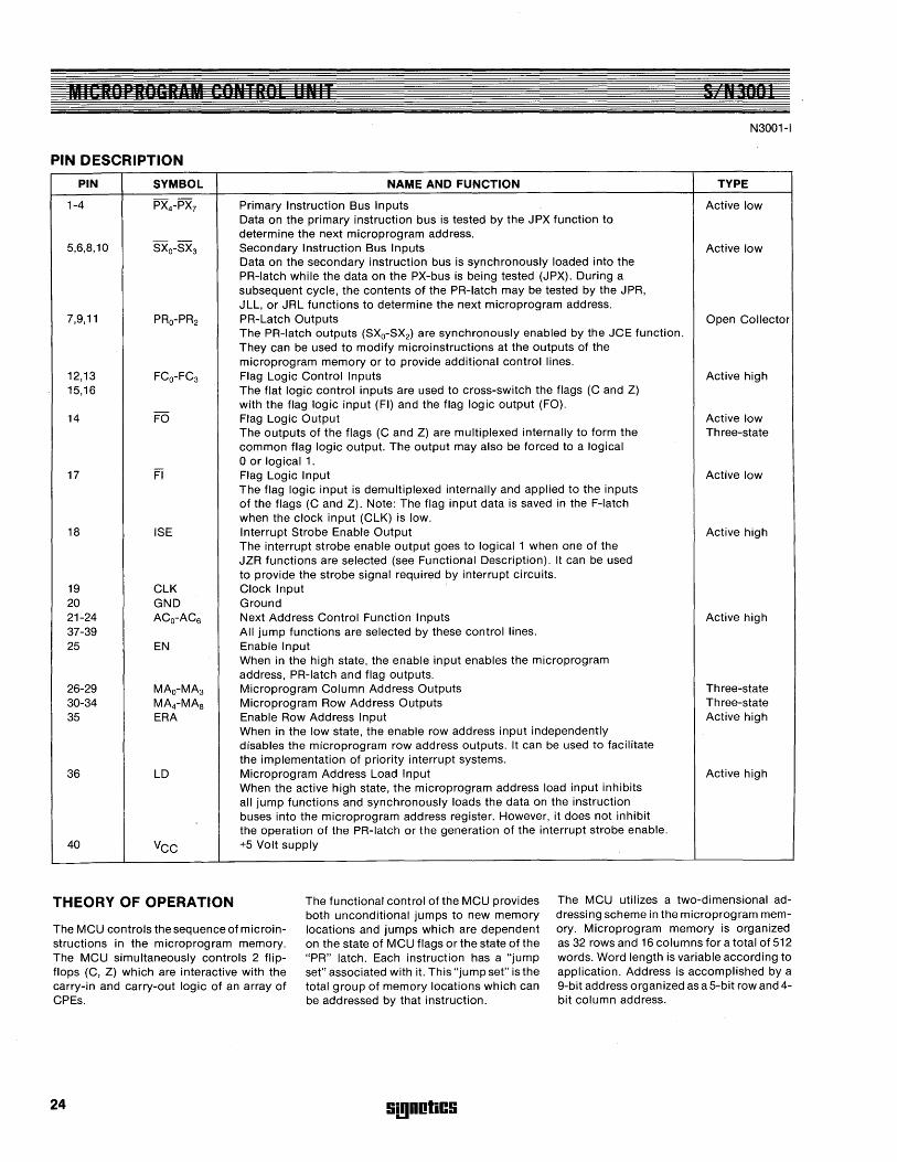
PIN DESCRIPTION
PIN SYMBOL NAME AND FUNCTION TYPE
1-4 PX4-PX7 Primary Instruction Bus Inputs Active low Data on the primary instruction bus is tested by the JPX function to determine the next microprogram address.
5,6,8,10 SXO-SX3 Secondary Instruction Bus Inputs Active low Data on the secondary instruction bus is synchronously loaded into the PR-Iatch while the data on the PX-bus is being tested (JPX). During a subsequent cycle, the contents of the PR-Iatch may be tested by the JPR, JLL, or JRL functions to determine the next microprogram address.
7,9,11 PRo-PR2 PR-Latch Outputs Open Collector The PR-Iatch outputs (SXO-SX2) are synchronously enabled by the JCE function. They can be used to modify microinstructions at the outputs of the microprogram memory or to provide additional control lines.
12,13 FCo-FC3 Flag Logic Control Inputs Active high 15,16 The flat logic control inputs are used to cross-switch the flags (C and Z)
with the flag logic input (FI) and the flag logic output (FO). 14 FO Flag Logic Oulput Active low
The outputs of the flags (C and Z) are multiplexed internally to form the Three-state common flag logic output. The output may also be forced to a logical o or logical 1.
17 fi Flag Logic Input Active low The flag logic input is demultiplexed internally and applied to the inputs of the flags (C and Z). Note: The flag input data is saved in the F-Iatch when the clock input (CLK) is low.
18 ISE Interrupt Strobe Enable Output Active high The interrupt strobe enable output goes to logical 1 when one of the JZR functions are selected (see Functional Description). It can be used to provide the strobe signal required by interrupt circuits.
19 CLK Clock Input 20 GND Ground 21-24 ACo-AC6 Next Address Control Function Inputs Active high 37-39 All jump functions are selected by these control lines. 25 EN Enable Input
When in the high state, the enable input enables the microprogram address, PR-Iatch and flag outputs.
26-29 MAo-MA3 Microprogram Column Address Outputs Three-state 30-34 MA4-MAs Microprogram Row Address Outputs Th ree-state 35 ERA Enable Row Address Input Active high
When in the low state, the enable row address input independently disables the microprogram row address outputs. It can be used to facilitate the implementation of priority interrupt systems.
36 LD Microprogram Address Load Input Active high When the active high state, the microprogram address load input inhibits all jump functions and synchronously loads the data on the instruction buses into the microprogram address register. However, it does not inhibit the operation of the PR-Iatch or the generation of the interrupt strobe enable.
40 VCC +5 Volt supply
THEORY OF OPERATION
The MCU controls the sequence of microinstructions in the microprogram memory. The MCU simultaneously controls 2 flipflops (C, Z) which are interactive with the carry-in and carry-out logic of an array of CPEs.
The functional control of the MCU provides both unconditional jumps to new memory locations and jumps which are dependent on the state of MCU flags or the state of the "PR" latch. Each instruction has a "jump set" associated with it. This "jump set" is the total group of memory locations which can be addressed by that instruction.
The MCU utilizes a two-dimensional addressing scheme in the microprogram memory. Microprogram memory is organized as 32 rows and 16 columns for a total of 512 words. Word length is variable according to application. Address is accomplished by a 9-bit add ress organ ized as a 5-bit row and 4-bit column address.
24 Gi!lDotiCG
MICkOPROGRAM CON I kOL UNII S N3001
ADDRESSING ORGANIZATION
32
ROWSr+~~~~+-r+~+-~~~
1 ... ---- 16 COLUMNS -----\
MAO-MA3
FUNCTIONAL DESCRIPTION The following is a description of each of the eleven address control functions. The symbols shown below are used to specify row and column addresses.
SYMBOL MEANING
rown 5-bit next row address where n is the decimal rowaddress.
col n 4-bit next column address where n is the decimal column address.
Unconditional Address Control (Jump) Functions The jump functions use the current microprogram address (i.e., the contents of the microprogram address register prior to the rising edge of the clock) and several bits from the address control inputs (ACO-AC6) to generate the next microprogram address.
Flag Conditional Address Control (Jump Test) Functions The jump/test flag functions use the current microprogram address, the contents of the selected flag or latch, and several bits from the address control function to generate the next microprogram address.
N3001-1
JUMP FUNCTION TABLE
MNEMONIC
JCC
JZR
JCR
JCE
FUNCTION DESCRIPTION
Jump in current column. ACo-AC4 are used to select 1 of 32 row addresses in the current column, specified by MAo-MA3' as the next address.
Jump to zero row. ACo-AC3 are used to select 1 of 16 column addresses in rowo, as the next address.
Jump in current row. ACo-AC3 are used to select 1 of 16 addresses in the current row, specified by MA4-MAs, as the next address.
Jump in current column/row group and enable PR-Iatch outputs. ACo-AC2 are used to select 1 of 8 row addresses in the current row group, specified by MA?-MAs, as the next row address. The current column is specified by MAo-MA3. The PR-Iatch outputs are asynchronously en-
. abled.
JUMP/TEST FUNCTION TABLE
MNEMONIC FUNCTION DESCRIPTION
JFL Jump/test F-Iatch. ACo-AC3 are used to select 1 of 16 row addresses in the current row group, specified by MAs, as the next row address. If the current column group, specified by MA3, is colo-col?, the F-Iatch is used to select col2 or col3 as the next column address. If MA3 specifies column group cols-coI 15 , the F-Iatch is used to select COllO or COlll as the next column address.
JCF
JZF
JPR
JLL
JRL
JPX
Jump/test C-flag. ACo-AC2 are used to select 1 of 8 row addresses in the current row group, specified by MA? and MAs, as the next row address. If the current column group specified by MA3 is colo-col?, the C-flag is used to select col2 or col3 as the next column address. If MA3 specifies column group cols-coI 15 , the C-flag is used to select col lO or COlll as the next column address.
Jump/test Z-flag. Identical to the JCF function described above, except that the Z-flag, rather than the C-flag, is used to select the next column address.
Jump/test PR-Iatch. ACo-AC2 are used to select 1 of 8 row addresses in the current row group, specified by MAl and MAs, as the next row address. The 4 PR-Iatch bits are used to select 1 of 16 possible column addresses as the next column address.
Jump/test leftmost PR-Iatch bits. ACo-AC2 are used to select 1 of 8 row addresses in the current row group, specified by MAl and MAs, as the next row address. PR2 and PR3 are used to select 1 of 4 column addresses in col 4 through col? as the next column address.
Jump/test rightmost PR-Iatch bits. ACo and ACl are used to select 1 of4 high-order row addresses in the current row group, specified by MA? and MAs, as the next row address. PRo and PRl are used to select 1 of 4 possible column addresses in COl 12 through COl 16 as the next column address.
Jump/test PX-bus and load PR-Iatch. ACo and ACl are used to select 1 of 4 row addresses in the current row group, specified by MA6-MAs, as the next row address. PX4-PXl are used to select 1 of 16 possible column addresses as the next column address. SXO-SX3 data is locked in the PRlatch at the rising edge of the clock.
SmDotiCS 25
MICROPROGRAM CONTROE BNIT S N3oo1
PX-Bus and PR-Latch Conditional Address Control (Jump/Test) Functions The PX-bus jump/test function uses the data on the primary instruction bus (PX4-
PX7), the current microprogram address, and several selection bits from the address control function to generate the next microprogram address. The PR-Iatch jump/ test functions use the data held in the PRlatch, the current microprogram address, and several selection bits from the address control function to generate the next microprogram address.
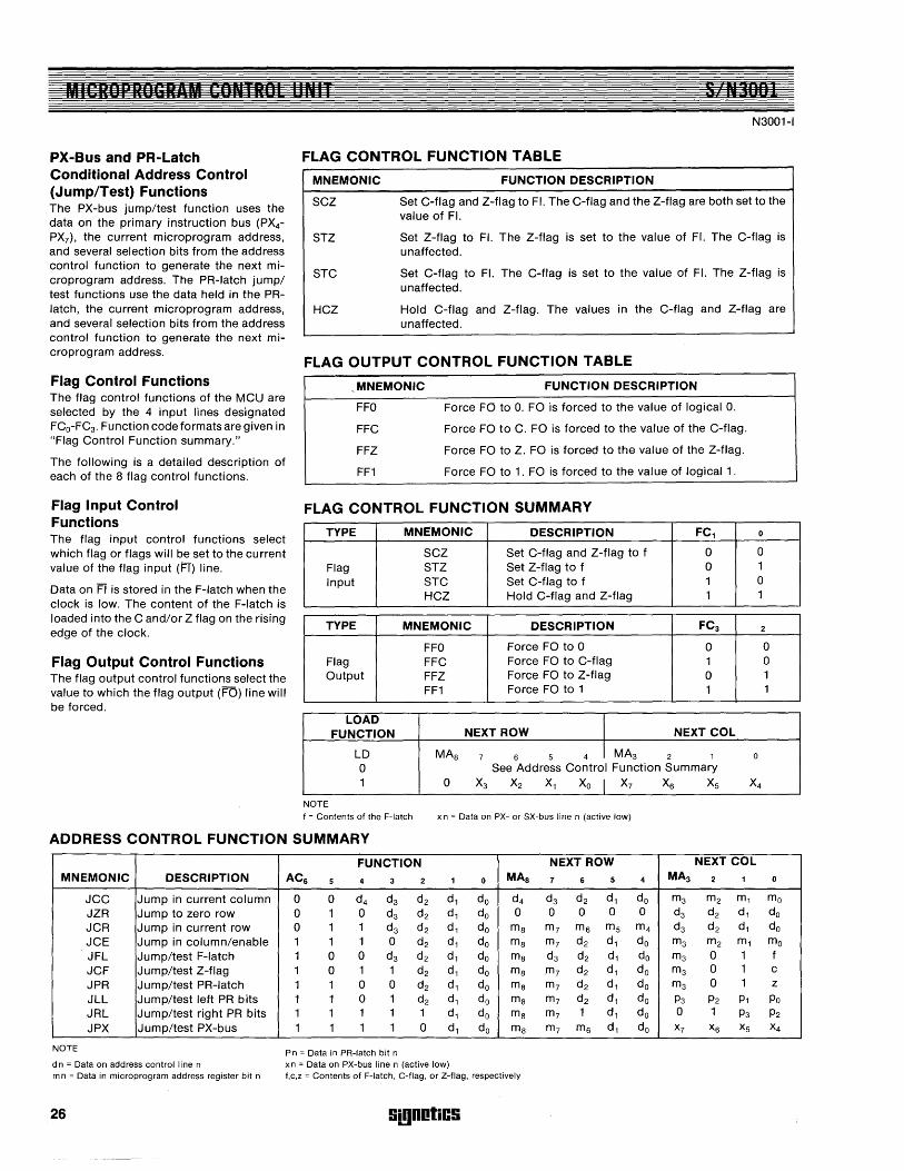
Flag Control Functions The flag control functions of the MCU are selected by the 4 input lines designated FCo-FC3. Function code formats are given in "Flag Control Function summary."
The following is a detailed description of each of the 8 flag control functions.
Flag Input Control Functions The flag input control functions select which flag or flags will be set to the current value of the flag input (FI) line.
Data on Fi is stored in the F-Iatch when the clock is low. The content of the F-Iatch is loaded into the C and/or Z flag on the rising edge of the clock.
Flag Output Control Functions The flag output control functions select the value to which the flag output (FO) line will be forced.
N3001-1
FLAG CONTROL FUNCTION TABLE
MNEMONIC FUNCTION DESCRIPTION
SCZ Set C-flag and Z-flag to FI. The C-flag and the Z-flag are both set to the value of FI.
STZ Set Z-flag to FI. The Z-flag is set to the value of FI. The C-flag is unaffected.
STC Set C-flag to FI. The C-flag is set to the value of FI. The Z-flag is unaffected.
HCZ Hold C-flag and Z-flag. The values in the C-flag and Z-flag are unaffected.
FLAG OUTPUT CONTROL FUNCTION TABLE
,MNEMONIC FUNCTION DESCRIPTION
FFO Force FO to O. FO is forced to the value of logical O.
FFC Force FO to C. FO is forced to the value of the C-flag.
FFZ Force FO to Z. FO is forced to the value of the Z-flag.
FF1 Force FO to 1. FO is forced to the value of logical 1.
FLAG CONTROL FUNCTION SUMMARY
TYPE MNEMONIC DESCRIPTION FC1 0
SCZ Set C-flag and Z-flag to f 0 0 Flag STZ Set Z-flag to f 0 1 Input STC Set C-flag to f 1 0
HCZ Hold C-flag and Z-flag 1 1
TYPE MNEMONIC DESCRIPTION FC3 2
FFO Force FO to 0 0 0 Flag FFC Force FO to C-flag 1 0 Output FFZ Force FO to Z-flag 0 1
FF1 Force FO to 1 1 1
LOAD FUNCTION NEXT ROW NEXT COL
LD MAa 7 6 s 4 MA3 2 1 0
0 See Address Control Function Summary 1 0 X3 X2 X1 Xo I X7 X6 Xs X4
NOTE
f = Contents of the F-Iatch x n = Data on PX- or SX-bus line n (active low)
ADDRESS CONTROL FUNCTION SUMMARY
FUNCTION NEXT ROW NEXT COL MNEMONIC DESCRIPTION AC6 5 4 3 2 1 0 MAs 7 6 5 4 MA3 2 1 0
JCC Jump in current column 0 0 d4 d3 d2 d1 do d4 d3 d2 d1 do m3 m2 m1 mo JZR Jump to zero row 0 1 0 d3 d2 d1 do 0 0 0 0 0 d3 d2 d1 do JCR Jump in current row 0 1 1 d3 d2 d1 do ma m7 m6 ms m4 d3 d2 d1 do JCE Jump in column/enable 1 1 1 0 d2 d1 do ma m7 d2 d1 do m3 m2 m1 mo JFL Jump/test F-Iatch 1 0 0 d3 d2 d1 do ma d3 d2 d1 do m3 0 1 f JCF Jump/test Z-flag 1 0 1 1 d2 d1 do ma m7 d2 d 1 do m3 0 1 c
JPR Jump/test PR-Iatch 1 1 0 0 d2 d1 do ma m7 d2 d1 do m3 0 1 z
JLL Jump/test left PR bits 1 1 0 1 d2 d1 do ma m7 d2 d1 do P3 P2 P1 Po JRL Jump/test right PR bits 1 1 1 1 1 d1 do ma m7 1 d1 do 0 1 P3 P2 JPX Jump/test PX-bus 1 1 1 1 0 d1 do ma m7 m6 d1 do x7 X6 Xs x4
NOTE Pn = Data in PR-Iatch bit n d n = Data on address control line n xn = Data on PX-bus line n (active low) mn = Data in microprogram address register bit n f,c,z = Contents of F-Iatch, C-flag, or Z-flag, respectively
26 smAoties
MICROPRIIGkAM OONTROL UNII
STROBE FUNCTIONS The load function of the MCU is controlled by the input line designated LD. If the LD line is active high at the rising edge of the clock, the data on the primary and secondary instruction buses, PXr PX7 and SXO-SX3' is loaded into. the microprogram address register. PX4-PX7 are loaded into MAo-MA7 and SXd-SX3 are loaded into MA4-MA7. The high-order bit of the microprogram address register MAs is set to a logical O. The bits from the primary instruction bus select 1 of 16 possible column addresses. Likewise, the bits from the secondary instruction bus select 1 of the fi rst 16 row add resses.
The MCU generates an interrupt strobe enable on the output line designated ISE. The line is placed in the active high state whenever a JZR to COilS is selected as the address control function. Generally, the start of a macroinstruction fetch sequence is situated at rowo and COilS so the interrupt control may be enabled at the beginning of the fetch/execute cycle. The interrupt control responds to the interrupt by pulling the enable row address (ERA) input line low to override the selected next row address from the MCU. Then by gating an alternative next row address on to the row address lines of the microprogram memory, the microprogram may be forced to enter an interrupt handling routine. The alternative row address placed on the microprogram memory address lines does not alter the contents of the microprogram address register. Therefore, subsequent jump functions will utilize the row address in the register, and not the alternative row address, to determine the next microprogram address.
Note, the load function always oVerrides the address control function on ACo-AC6 . It does not, however, override the latch enable or load sUb-functions of the JCE or JPX instruction, respectively. In addition, it does not inhibit the interrupt strobe enable or any of the flag control functions.
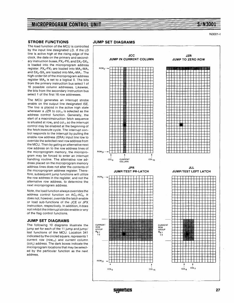
JUMP SET DIAGRAMS The following 10 diagrams illustrate the jump set for each of the 11 jump and jump/ test functions of the MCU. Location 341 indicated by the circled square, represents 1 current row (row2l ) and current column (co Is) address. The dark boxes indicate the microprogram locations that may be selected by the particular function as the next address.
JUMP SET DIAGRAMS
JCC JUMP IN CURRENT COLUMN
(
'of
ROW3l -- L.....L.....L...L..JL......&i_.J.........L-L...1.-1-..L-L...L..-JL.......J
CURRENT ROW GROUP MS7
10
t COlO
COlO
t t CURRENT COl15 COLUMN
JPR JUMP/TEST PR-LATCH
!ii!)notiC!i
CURRENT ROW GROUP MS 7
10
S N3DOI
N3001-1
JZR JUMP TO ZERO ROW
(.
JLL JUMP/TEST LEFT LATCH
f-f-
il f-I-f-f-f-f-f-f-f-I-1-1-f-f-I-r-
27
MICROPROGRAM CONTROL UNIT
JUMP SET DIAGRAMS (Cont'd)
CURREN;LROW GROUP MS76
101 S--
28
CURRENT ROW GROUP MS 7
10
JRL JUMP/TEST RIGHT LATCH
~
.IJ
JCE JUMP COLUMN/ENABLE
CURRENT COLUMN
CURREN;lROW GROUP MS76
101 S-
CURRENT ROW GROUP MS
1
JPX JUMP/TEST PX-BUS
r+-r~-+~+;-r~~-r~r;
----------I--I--I--I--I--I--
--
JFL JUMP/TEST F-LATCH
CURRENT COLUMN GROUP M3= 0
~
• r-
!ii!Jn~liC!i
CURRENT --+ROW
t
S N3110!
N3001-1
JCR JUMP IN CURRENT ROW
~
~
t COlO COl15
CURRENT ROW GROUP MS7
10
JCF, JZF JUMP/TEST C-FLAG JUMP/TEST Z-FLAG
CURRENT COLUMN GROUP M3= o·
!I .) r-
i bOl3 (c,z = 1) COl2 (c,z = 0)
MICROPkOGkAM CON I kOL UNIT
N3001 T A = O°C to +70°C, VCC = 5.0V, ± 5%
AC ELECTRICAL CHARACTERISTICS S3001 T A= -55°C to +125°C, VCC = 5.0V ± 10%
PARAMETER N3001
Min Typ1 Max
tCY Cycle Time2 60 45
tpw Clock Pulse Width 17 10 Control and Data Input Set-Up Times:
tSF lD, ACo-AC6 (Set to "1 "/"0") 20 3/14
tSK FCo, FC1 7 5
tsx PX4-PX7 (Set to "1 "/"0") 28 4/13
tSI FI (Set to "1 "/"0") 12 -6/0
tsx SXO-SX3 15 5 Control and Data Input Hold Times:
tHF lD, ACo-AC6 (Hold to "1 "/"0") 4 -3/-14
tHK FCo, FC1 4 -5
tHX PX4-PX7 (Hold to "1 "/"0") 0 -4/-13
tHI FI (Hold to "1 "/"0") 16 6.5/0
tHX SXO-SX3 0 -5
tco Propagation Delay from Clock Input (ClK) to Outputs 17/24 36 (mAo-mAs, Fa) (tPHl/tPlH)
t KO Propagation Delay from Control I n puts FC2 and FC3 to Flag 13 24 Out (Fa)
t FO Propagation Delay from Control Inputs ACo-AC6 to latch 21 32 Outputs (PRo-PR2)
tEO Propagation Delay from Enable Inputs EN and ERA to 17 26 Outputs (mAo-mAs, Fa, PRo-PR2 )
tFI Propagation Delay from Control Inputs ACo-AC6 to 20 32 IlJterrupt Strobe Enable Output (ISE)
NOTE
1. Typical values are for T A = 25°C and 5.0 supply voltage. 2. 83001: tCY = tWP + t8F + tCO
!ii!lDotiC!i
S N3001
N3001-1
53001
Min Typ1 Max UNIT
95 45 ns 40 10 ns
20 3/14 ns 10 5 ns 35 4/13 ns 15 -6/10 ns 35 5 ns
5 -3/-14 ns 10 -5 ns 25 -4/-13 ns 22 6.5/0 ns 25 -5 ns 10 17/24 45 ns
13 50 ns
21 50 ns
17 35 ns
20 40 ns
29
M IE"OI liOGItAII bOIi I hOL tJ N II
VOLTAGE WAVEFORMS
CLK CLOCK INPUT
EN, ERA ENABLE INPUTS
~~~~~~~ MEMORY ADDRESS OUTPUTS
PR O-PR 2 "PR" LATCH OUTPUTS
FCO-FC3 FLAG CONTROL INPUTS
FI FLAG INPUT
~ ~
V / .
\1/ / 1\
-tco -
.
-tHK
\
tCY
tEO --\ V /\
tHF tSF_
\V J~
tEO
- tFO I-
\V J~
tSK
\ V /1\
tHI tSI
\ V J\
_tKO I---tEO
FO FLAG OUTPUT
ISE INTERRUPT STROBE ENABLE OUTPUT
I-tco
I\V lI\ _tFI ___
\/
S N 30"}
N3001-1
if 1\ J _tpw ____
I----
SXO-PX7 ___________________ I~.~~ __ -_-_-_-__ t_HX __ -_-_-_-_-_"~:I~-~.-'-____ ~ ______ ts_x __ ~ ___ ------.~I----------------------~ INSTRUCTION A BUS INPUTS
30 Si!lDOliCS
GLN I RAL PltuGESSING ELEMENI S Hal102
S3002-1 • N3002-XL, I
DESCRIPTION The N3002 Central Processing Element (CPE) is one part of a bipolar microcomputer set. The N3002 is organized as a 2-bit slice and performs the logical and arithmetic functions required by microinstructions. A system with any number of bits in a data word can be implemented by using multiple N3002s, the N3001 microcomputer control unit, the N74S182 carry look-ahead unit and ROM or PROM memory.
FEATURES • 45ns cycle time (typ) • Easy expansion to multiple of 2 bits • 11 general purpose registers • Full function accumulator • Useful functions include:
• 2's complement arithmetic • Logical AND, OR, NOT, exclusive-
NOR • Increment, decrement • Shift left/shift right • Bit testing and zero detection • Carry look-ahead generation • Masking via K-bus • Conditioned clocking allowing non
destructive testing of data in accumulator and scratch pad
• 3 input buses • 2 output buses • Control bus
BLOCK DIAGRAM (12)
FUNCTION TRUTH TABLE
FUNCTION GROUP Fs Fs
0 0 0 1 a a 2 a 1 3 a 1 4 1 a 5 1 0 6 1 1 7 1 1
REGISTER GROUP REGISTER F3 F2
Ro 0 a Rl 0 a R2 a 0 R3 0 0 R4 a 1
I R5 a 1 R6 0 1 R7 0 1 R8 1 0 Rg 1 a T 1 1
AC 1 1
II T 1 0 AC 1 0
III T 1 1
AC 1 1
(13) (20) (19)
PIN CONFIGURATION
XL,I PACKAGE
F4
a 1 a 1 a 1 a 1
Fl Fo
a a a 1 1 0 1 1 a 0 a 1 1 a 1 1 a 0 0 1 0 0 0 1
1 a 1 1
1 0 1 1
(11)0--a----J '-------------lo-~(23) EA ED
(S) Xo----1f-----________ ...r-......... ..L....--......... ---L....------, (6) yo-___ !--------------I ... ----+---+---4---1f----lO--C CI (10)
(7) COo--oI-------------I 1----I----+---l~I__-_h__<l RO (8)
(9) LI o--qt------------~-""T""r------""T"""r_~ (18) CLKo--oI (28) VCco---t (14) GNDO---;
(lS) F60---t-----t (16) FSo---t-----t (17) F 4 0----4-----t (24) F30---t-----t (27) F20----4-----t (26) Fl o-___ f----~ (2S) FO o-___ f----___
FUNCTION DECODER
L _________ _
Ml MO (21) (22)
Smnotics
I I I I I I I I I I
--______ -.J
31
G(UTNAt P luGE iSING ELEMENT S Nann, S3002-1 • N3002-Xl,1
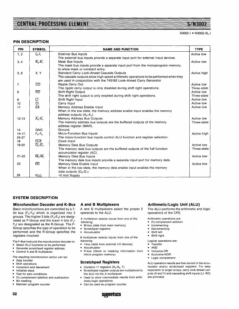
PIN DESCRIPTION
PIN SYMBOL NAME AND FUNCTION TYPE
1,2 ~-G External Bus Inputs Active low The external bus inputs provide a separate input port for external input devices.
3,4 Ko-i<-t Mask Bus I n puts Active low The mask bus inputs provide a separate input port from the microprogram memory, to allow mask or constant entry.
5, 6 X, Y Standard Carry look-Ahead Cascade Outputs Active high The cascade outputs allow high speed arithmetic operations to be performed when they are used in conjunction with the 74S182 look-Ahead Carry Generator
7 CO Ripple Carry Out Active low The ripple carry output is only disabled during shift right operations. Three-state
8 RO Shift Right Output Active low The shift right output is only enabled during shift right operations. Th ree-state
9 IT Shift Right Input Active low 10 a Carry Input Active low 11 EA Memory Address Enable Input Active low
When in the low state, the memory address enable input enables the memory address outputs (Ao-A1).
12-13 Ao-~ Memory Address Bus Outputs Active low The memory address bus outputs are the buffered outputs of the memory Three-state address register (MAR).
14 GND Ground 14-17, Fo-Fe Micro-Function Bus Inputs Active high 24-27 The micro-function bus inputs control AlU function and register selection. 18 ClK Clock Input 19-20 ~-~ Memory Data Bus Outputs Active low
The memory data bus outputs are the buffered outputs of the full function Th ree-state accumulator register (AC).
21-22 Mo-M1 Memory Data Bus Inputs Active low The memory data bus inputs provide a separate input port for memory data.
23 ED Memory Data Enable Input Active low When in the low state, the memory data enable input enables the memory data outputs (00-01).
28 VCC +5 Volt Supply
SYSTEM DESCRIPTION
Microfunction Decoder and K-Bus Basic microfunctions are controlled by a 7-bit bus (Fo-Fe) which is organized into 2 groups. The higher 3 bits (F 4-Fe) are designated as F-Group and the lower 4 bits (FoF3) are designated as the R-Group. The FGroup specifies the type of operation to be performed and the R-Group specifies the registers involved.
A and B Multiplexers Arithmetic/Logic Unit (ALU)
The F-Bus instructs the microfunction decoder to: • Select ALU functions to be performed • Generate scratch pad register address • Control A and B multiplexer
The resulting microfunction action can be: • Data transfer • Shift operations • Increment and decrement • Initialize stack • Test for zero conditions • 2's complement addition and subtraction • Bit masking • Maintain program counter
32
A and B multiplexers select the proper 2 operands to the AlU.
A multiplexer selects inputs from one of the following: • M-bus (data from main memory) • Scratch pad registers • Accumulator
B multiplexer selects inputs from one of the following: • I-bus (data from external I/O devices) • Accumulator • K-bus (literal or masking information from
micro-program memory)
Scratch pad Registers • Contains 11 registers (Ro-Rg, T) • Scratchpad register outputs are multiplexed to
the ALU via the A multiplexer • Used to store intermediate results from arith
metic/logic operations • Can be used as program counter
G!!IDOliCG
The AlU performs the arithmetic and logic operations of the CPE.
Arithmetic operations are: • 2's complement addition • Incrementing • Decrementing • Shift left • Shift right
Logical operations are: • Transfer • AND • Inclusive-OR • Exclusive-NOR • Logic complement
ALU operation results are then stored in the accumulator and/or scratch pad registers. For easy expansion to larger arrays, carry look-ahead outputs (X and Y) and cascading shift inputs (LI, RO) are provided.
12tH I Kill I'KIiItESSING ElEMEN I S N3602
Accumulator • Stores results from ALU operations
• Accepts 2 bits of data from external input/output devices into CPE
S3002-1 • N3002-XL,1
Output Buses
• The output of accumulator is multiplexed into ALU via the A and B multiplexer as one of the operands
• Is multiplexed into the ALU via the B multiplexer
K-bus: A special feature of the N3002 CPE
A-bus and Memory Address Register • Main memory address is stored in the memory
address register (MAR) • Main memory is addressed via the A-bus
Input Buses M-bus: Data bus from main memory
• During arithmetic operations, the K-bus can be used to mask portions of the field being operated on
• MAR and A-bus may also be used to generate device address when executing 1/00 instrucinstructions
• A-bus has Tri-State outputs
• Accepts 2 bits of data from main memory into CPE
• Select or remove accumulator from operation by placing K-bus in all "1" or all "0" state respectively
• During non-arithmetic operation, the carry circuit can be used in conjunction with the K-bus for word-wise-OR operation for bit testing
D-bus: Data bus from CPE to main memory or to 1/0 devices • Is multiplexed into the ALU via the A multi
plexer • Sends buffered accumulator outputs to main memory or the external 1/0 devices
I-bus: Data bus from input/output devices • Supply literal or constant data to CPE • D-bus has Tri-State outputs
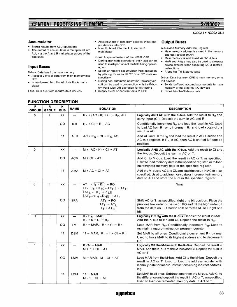
FUNCTION DESCRIPTION F R K
NAME EQUATION DESCRIPTION GROUP GROUP BUS
0 I XX - Rn + (AC AK) + CI ..... Rn, AC Logically AND AC with the K-bus. Add the result to R nand carry input (CI). Deposit the sum in AC and R n.
00 ILR Rn+CI ..... R ,AC Conditionally increment R n and load the result in AC. Used to load AC from R n or to increment R n and load a copy of the result in AC.
11 ALR AC+Rn+CI ..... Rn,AC Add AC and CI to R n and load the result in AC. Used to add AC to a register. If R n is AC, then AC is shifted left one bit position.
0 II XX - M + (AC A K) + CI ..... AT Logicany AND AC with the K-bus. Add the result to CI and the M-bus. Deposit the sum in AC or T.
00 ACM M + CI ..... AT Add CI to M-bus. Load the result in AC or T, as specified. Used to load memory data in the specified register, or to load incremented memory data in the specified register.
11 AMA M + AC + CI ..... AT Add the M-bustoACand CI, and load the result in ACorT, as specified. Used to add memory data or incremented memory data to AC and store the sum in the specified register.
0 III XX - ATL A(ILA KL) ..... RO None Llv [(IH/\ KH)AATH] ..... ATH [ATL A (I L A KUJ [ATHv(IH AKH)] ..... ATL
00 SRA ATL ..... RO Shift AC or T, as specified, right one bit position. Place the ATH ..... ATL previous low order bit value on RO and fill the high order bit
LI ..... ATH from the data on LI. Used to shift or rotate AC or T right one bit.
1 I XX - Kv Rn ~ MAR Logically OR R n with the K-bus. Deposit the result in MAR. Rn+K+CI ..... Rn Add the K-bus to R nand CI. Deposit the result in R n.
00 LMI Rn ..... MAR, Rn+CI ..... Rn Load MAR from R n. Conditionally increment R n. Used to maintain a macro-instruction program counter.
11 DSM 11 ..... MAR, Rn-1+CI ..... Rn Set MAR to all ones. Conditionally decrement R n by one. Used to force MAR to its highest address and to decrement Rn.
1 II XX - KVM ..... MAR Logically OR the M-bus with the K-Bus. Deposit the result in M + K + CI ..... AT MAR. Add the K-bus to the M-bus and CI. Deposit the sum in
AC or T.
00 LMM M ..... MAR, M + CI ..... AT Load MAR from the M-bus. Add CI to the M-bus. Deposit the result in AC or T. Used to load the address register with memory data for macro-instructions using indirect address-ing.
11 LDM 11 ..... MAR Set MAR to all ones. Subtract one from the M-bus. Add CI to M - 1 + CI ..... AT the difference and deposit the result in AC or T, as specified.
Used to load decremented memory data in AC or T.
!i!!lDotiC!i 33
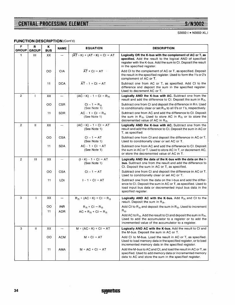
tEIiTRIL PROCESSING ELEMENT S N3002
S3002-1 • N3002-XL, I
FUNCTION DESCRIPTION (Cont'd)
F R K NAME EQUATION DESCRIPTION GROUP GROUP BUS
1 III XX - (AT v K) + (AT t\ K) + CI ..... AT Logically OR the K-bus with the complement of AC or T, as specified. Add the result to the logical AND of specified register with the K-bus. Add the sum to CI. Deposit the result in the specified register.
00 CIA AT + CI ..... AT Add CI to the complement of AC or T, as specified. Deposit the result in the specified register. Used to form the 1 's or 2's complement of AC or T.
11 DCA AT - 1 + CI ..... AT Subtract one from AC or T, as specified. Add CI to the difference and deposit the sum in the specified register. Used to decremenf AC or T.
2 I XX - (AC t\ K) - 1 + CI ..... R n Logically AND the K-bus with AC. Subtract one from the result and add the difference to CI. Deposit the sum in R n.
00 CSR CI-1 ..... Rn Subtract one from CI and deposit the difference in R n. Used (See Note 1) to conditionally clear or set R n to all O's or 1 's, respectively.
11 SDR AC-1+CI ..... Rn Subtract one from AC and add the difference to CI. Deposit (See Note 1) the sum in R n. Used to store AC in R n or to store the
decremented value of AC in R n.
2 II XX - (AC t\ K) - 1 + CI ..... AT Logically AND the K-bus with AC. Subtract one from the (See Note 1) result and add the difference to CI. Deposit the sum in AC or
T, as specified.
00 CSA CI - 1 ..... AT Subtract one from CI and deposit the difference in AC or T. (See Note 1) Used to conditionally clear or set AC or T.
11 SDA AC - 1 + CI ..... AT Subtract one from AC and add the difference to CI. Deposit (See Note 1) the sum in AC or T. Used to store AC in T, or decrement AC,
or store the decremented value of AC in T.
2 III XX - (I t\ K) - 1 + CI ..... AT Logically AND the data of the K-bus with the data on the 1-(See Note 1) bus. Subtract one from the result and add the difference to
CI. Deposit the sum in AC or T, as specified.
00 CSA CI - 1 ..... AT Subtract one from CI and deposit the difference in AC or T. Used to conditionally clear or set AC or T.
11 LDI 1-1 + CI ..... AT Subtract one from the data on the I-bus and add the differ-ence to CI. Deposit the sum in AC or T, as specified. Used to load input bus data or decremented input bus data in the specified register.
3 I XX - R n + (AC t\ K) + CI ..... R n Logically AND AC with the K-bus. Add R nand CI to the result. Deposit the sum in Rn.
00 INR Rn + CI ..... Rn Add CI to R n and deposit the sum in R n. Used to increment
11 ADR AC+Rn+CI ..... Rn Rn·
Add AC to R n. Add the result to CI and deposit the sum in R n. Used to add the accumulator to a register or to add the incremented value of the accumulator to a register.
3 II XX - M + (ACt\ K) + CI ..... AT Logically AND AC with the K-bus. Add the result to CI and the M-bus. Deposit the sum in AC or T.
00 ACM M + CI ..... AT Add CI to M-bus. Load the result in AC or T, as specified. Used to load memory data in the specified register, or to load incremented memory data in the specified register.
11 AMA M + AC + CI ..... AT Add the M-bus to AC and CI, and load the result in AC orT, as specified. Used to add memory data or incremented memory data to AC and store the sum in the specified register.
34 Si!)DotiCS
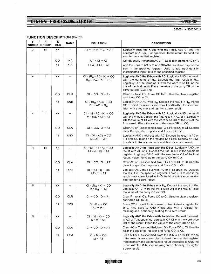
'E"IlniE PROCESSING EEEMENI S M3ullz
83002-1 • N3002-Xl,1
FUNCTION DESCRIPTION (Cont'd)
F R K NAME EQUATION DESCRIPTION GROUP GROUP BUS
3 III XX - AT + (1/\ K) + CI - AT Logically AND the K-bus with the I-bus. Add CI and the contents of AC or T, as specified, to the result. Deposit the sum in the specified register.
00 INA AT + CI - AT Conditionally increment AC or T. Used to increment AC or T.
11 AlA I+AT+CI-AT Add the I-bus to AC or T. Add CI to the result and deposit the sum in the specified register. Used to add input data or incremented input data to the specified register.
4 I XX - CI v (Rn /\ AC /\ K) - CO Logically AND the K-bus with AC. logically AND the result R n /\ (AC /\ K) - R n with the contents of R n. Deposit the final result in R n.
logically OR the value of CI with the word-wise OR of the bits of the final result. Place the value of the carry OR on the carry output (CO) line.
00 ClR CI- CO, 0- Rn Clear R n to all a's. Force CO to CI. Used to clear a register and force CO to CI.
11 ANR CI v (R n /\ AC) - CO logically AND AC with R n. Deposit the result in R n. Force Rn /\ AC - Rn CO to one if the result is non-zero. Used to AN D the accumu-
lator with a register and test for a zero result.
4 II XX - CI v (M /\ AC /\ K) - CO Logically AND the K-bus with AC. logically AND the result M /\ (AC /\ K) - AT with the M-bus. Deposit the final result in AC or T. Logically
OR the value of CI with the word-wise OR of the bits of the final result. Place the value of the carry OR on CO.
00 ClA CI- CO, a -AT Clear AC or T, as specified, to all a's. Force CO to CI. Used to clear the specified register and force CO to CI.
11 ANM CI v (M /\ AC) - CO logically AND the M-bus with AC. Deposit the result in AC or M /\AC - AT T. Force CO to one if the result is non-zero. Used to AND M-
bus data to the accumulator and test for a zero result.
4 III XX - CI v (AT /\ 1 /\ K) - CO Logically AND the I-bus with the K-bus. logically AND the AT /\ (I /\ K) - AT result with AC or T. Deposit the final result in the specified
register. logically OR CI with the word-wise OR of the final result. Place the value of the carry OR on CO.
00 CI-A CI- CO, a -AT Clear AC orT, as specified, to all a's. Force CO to CI. Used to clear the specified register and force CO to CI.
11 ANI Clv (AT/\I) - CO logically AND the I-bus with AC or T, as specified. Deposit AT/\1-AT the result in the specified register. Force CO to one if the
result is non-zero. Used to AND the I-bus to the accumulator and test for a zero result.
S I XX - CI v (Rn /\ K) - CO Logically AND the K-bus with Rn. Deposit the result in Rn. K/\Rn-Rn logically ORCI with the word-wise OR of the result. Place
the value of the carry OR on CO.
00 ClR CI- CO, 0- Rn Clear R n to all a's. Force CO to C I. Used to clear a reg ister and force CO to CI.
11 TZR CI vRn - CO Force CO to one if R n is non-zero. Used to test a register for Rn - Rn zero. Also used to AND K-bus data with a register for
masking and, optionally, testing for a zero result.
S II XX - CI v(M /\K) - CO Logically AND the K-bus with the M-bus. Deposit the result K /\ M - AT in AC or T, as specified. Logically OR CI with the word-wise
OR of the result. Place the value of the carry OR on CO.
00 ClA CI- CO, a -AT Clear AC orT, as specified, to all a's. Force CO to CI. Used to clear the specified register and force CO to CI.
11 lTM Clv M - CO Load AC or T, as specified, from the M-bus. Force CO to one M- AT if the result is non-zero. Used to load the specified register
from memory and test for a zero result. Also used to AND the K-bus with the M-bus for masking and, optionally, testing for a zero resu It.
Si!lDotiCS 35
CENTRAE PROCESSINB [EEMENT S N3 .... 2 S3002-1 • N3002-XL,1
FUNCTION DESCRIPTION (Cont'd)
F R K NAME EQUATION DESCRIPTION
GROUP GROUP BUS
5 III XX - CI v(AT !\K) - CO Logically AND the K-bus with AC or T, as specified. Deposit K!\AT-AT the result in the specified register. Logically OR CI with the
word-wise OR of the result. Place the value of the carry OR on CO.
00 CLA CI- CO, 0 -AT Clear AC arT, as specified, to all O's. Force CO to CI. Used to clear the specified register and force CO to CI.
11 TZA ClvAT-CO Force CO to one if AC or T, as specified, is non-zero. Used to AT- AT test the specified register for zero. Also used to AND the K-
bus to the specified register for masking and, optionally, testing for a zero result.
6 I XX - CI v (AC!\ K) - CO Logically OR CI with the word-wise OR of the logical AND of R n v (AC !\ K) - R n AC and the K-bus. Place the result of the carry OR on CO.
Logically OR R n with the logical AND of AC and the K-bus. Deposit the result in R n.
00 NOP CI-CO, Rn - Rn Force CO to CI. Used as a null operation orto force CO to CI.
11 ORR CI vAC - CO Force CO to one if AC is non-zero. Logically OR AC with R n. Rn v AC - Rn Deposit the result in R n. Used to OR the accumulator to a
register and, optionally, test the previous accumulator value for zero.
6 II XX - CI v(AC !\K) - CO Logically OR CI with the word-wise OR of the logical AND of M v (AC !\ K) - AT AC and the K-bus. Place the carry OR on CO. Logically OR
the M-bus, with the logical AND of AC and the K-bus. Deposit the final result in AC or T.
00 LMF CI - CO, M - AT Load AC or T, as specified, from the M-bus. Force CO to CI. Used to load the specified register with memory data and force CO to CI.
11 ORM Clv AC - CO Force CO to one if AC is non-zero. Logically OR the M-bus Mv AC - AT with AC. Deposit the result in AC or T, as specified. Used to
OR M-bus with the AC and, optionally, test the previous value of AC for zero.
6 III XX - CI v (I !\ K) - CO Logical OR CI with the word-wise OR of the logical AND of ATv(I!\I)-AT the I-bus and the K-bus. Place the carry OR on CO. Logically
AND the K-bus with the I-bus. Logically OR the result with AC or T, as specified. Deposit the final result in the specified register.
00 NOP CI - CO, AT - AT Force CO to CI. Used as a null operation orto force CO to CI.
11 ORI CI v I - CO Force CO to one if the data on the I-bus is non-zero. ~
IvAT-AT Logically OR the I-bus to AC or T, as specified. Deposit the result in the specified register. Used to OR I-bus data with the specified register and, optionally, test the I-bus data for zero.
7 I XX - CI v (R n !\ AC !\ K) - CO Logically OR CI with the word-wise OR of the logical AND of R n G5 (AC !\ K) - R n R nand AC and the K-bus. Place the carry OR on CO.
Logically AND the K-bus with AC. Exclusive-NOR the result with R n. Deposit the fi nal resu It in R n.
00 CMR CI-CO, Rn - Rn Complement the contents of R n. Force CO to CI.
11 XNR CI v(Rn!\ AC) - CO Force CO to one if the logical AND of ACand R n is non-zero.
Rn (±) AC - Rn Exclusive-NOR ACwith R n. Depositthe result in R n. Used to exclusive-NOR the accumulator with a register.
36 Si!lDOliCS
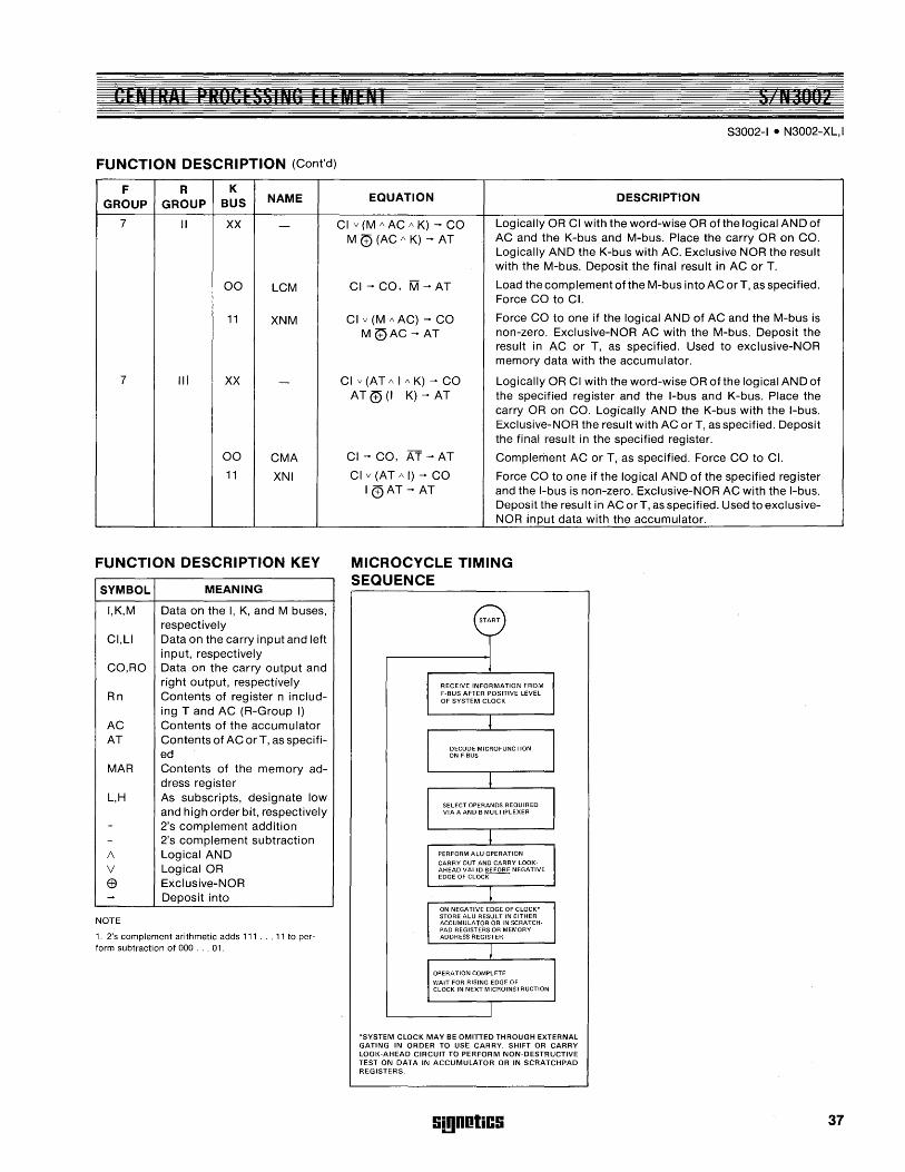
EEN I HAl PH[)(JESSINO ELEMEN I S N30il2
FUNCTION DESCRIPTION (Cont'd)
F R K GROUP GROUP BUS NAME
7 II XX -
00 LCM
11 XNM
7 III XX -
00 CMA
11 XNI
FUNCTION DESCRIPTION KEY
SYMBOL MEANING
I,K,M Data on the I, K, and M buses, respectively
CI,LI Data on the carry input and left input, respectively
CO,RO Data on the carry output and right output, respectively
Rn Contents of register n includ-ing T and AC (R-Group I)
AC Contents of the accumulator AT Contents of AC or T, as specifi-
ed MAR Contents of the memory ad-
dress register L,H As subscripts, designate low
and high order bit, respectively + 2's complement addition - 2's complement subtraction 1\ Logical AND V Logical OR ® Exclusive-NOR ..... Deposit into
NOTE
1. 2's complement arithmetic adds 111 ... 11 to perform subtraction of 000 ... 01.
S3002-1 • N3002-XL, I
EQUATION DESCRIPTION
CI v (M /\ AC /\ K) ..... CO Logically OR CI with the word-wise OR of the logical AND of M (±) (AC /\ K) ..... AT AC and the K-bus and M-bus. Place the carry OR on CO.
Logically AND the K-bus with AC. Exclusive NOR the result with the M-bus. Deposit the final result in AC or T.
CI ..... CO, Kif ..... AT Load the complement of the M-bus into AC or T, as specified. Force CO to CI.
CI v (M /\ AC) ..... CO Force CO to one if the logical AND of AC and the M-bus is M <VAC ..... AT non-zero. Exclusive-NOR AC with the M-bus. Deposit the
result in AC or T, as specified. Used to exclusive-NOR memory data with the accumulator.
CI V (AT/\ I /\K) ..... CO Logically OR CI with the word-wise OR of the logical AND of AT <±5 (I K) ..... AT the specified register and the I-bus and K-bus. Place the
carry OR on CO. Logically AND the K-bus with the I-bus. Exclusive-NOR the result with AC or T, as specified. Deposit the final result in the specified register.
CI ..... CO, AT ..... AT Complement AC or T, as specified. Force CO to CI.
Clv(AT/\I) ..... CO Force CO to one if the logical AND of the specified register I eAT"'" AT and the I-bus is non-zero. Exclusive-NOR AC with the I-bus.
Deposit the result in AC orT, as specified. Used to exclusive-NOR input data with the accumulator.
MICROCYCLE TIMING SEQUENCE
'SYSTEM CLOCK MAY BE OMITTED THROUGH EXTERNAL GATING IN ORDER TO USE CARRY, SHIFT OR CARRY LOOK-AHEAD CIRCUIT TO PERFORM NON-DESTRUCTIVE TEST ON DATA IN ACCUMULATOR OR IN SCRATCHPAD REGISTERS
S!!)DotiCS 37
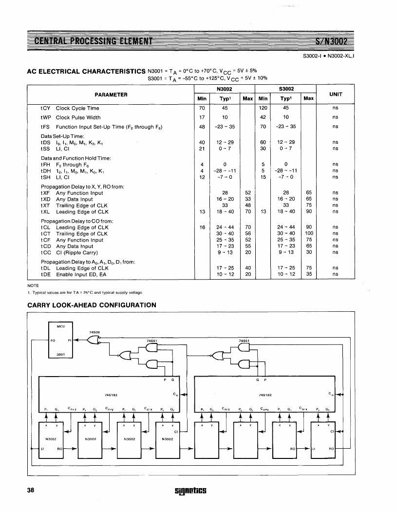
C 'T '"'' p" m' E S SIN G Fir Ii r NT
AC ELECTRICAL CHARACTERISTICS N3001 = T A = O°C to +70°C, VCC = 5V ± 5% S3001 = T A = -55°C to +125°C, V CC = 5V ± 10%
N3002 PARAMETER
Min Typ1 Max Min
tCY Clock Cycle Time 70 45 120
tWP Clock Pulse Width 17 10 42
tFS Function Input Set-Up Time (Fo through Fe) 48 -23 - 35 70
Data Set-Up Time: tDS 10' 11, Mo, M1, Ko, K1 40 12 - 29 60 tSS LI, CI 21 0-7 30
Data and Function Hold Time: tFH Fo through Fe 4 0 5 tbH 10, 11, Mo, M1, Ko, K1 4 -28 - -11 5 tSH LI, CI 12 -7 - 0 15
Propagation Delay to X, Y, RO from: tXF Any Function Input 28 52 tXD Any Data Input 16 - 20 33 tXT Trailing Edge of ClK 33 48 tXl leading Edge of ClK 13 18 - 40 70 13
Propagation Delay to CO from: tCl leading Edge of ClK 16 24 - 44 70 tCT Trailing Edge of ClK 30 - 40 56 tCF Any Function Input 25 - 35 52 tCD Any Data Input 17 - 23 55 tCC CI (Ripple Carry) 9 - 13 20
Propagation Delay to Ao, A1, Do, D1 from: tDl leading Edge of ClK 17 - 25 40 tDE Enable Input ED, EA 10 - 12 20
NOTE
1. Typical values are for T A = 25° C and typical supply voltage.
CARRY LOOK-AHEAD CONFIGURATION
MCU
74S08
FO FI
3001
P G G P
74S182
N3002 N3002 N3002
LI RO
38 S!!)notics
S ' JOOa S3002-1 • N3002-Xl,1
S3002 UNIT
Typ1 Max
45 ns
10 ns
-23 - 35 ns
12 - 29 ns 0-7 ns
0 ns -28 - -11 ns
-7 - 0 ns
28 65 ns 16 - 20 65 ns
33 75 ns 18 - 40 90 ns
24 - 44 90 ns 30 - 40 100 ns 25 - 35 75 ns 17 - 23 65 ns 9 - 13 30 ns
17 - 25 75 ns 10 - 12 35 ns
CI
RO
CENT' L PROCESSING ELEMENT
TYPICAL CONFIGURATIONS
/
S 1130llZ 83001-1 • N3002-XL,1
MEMORY ADDRESS BUS (2N LINES)
r.===========~---- / / - "\ DATA BUS TO MEMORY .,L-------l f----- r-V (2N LINES)
~---7~
CLOCK-----------------------~----++----._--------++----_H~--~-~7
Fa- F, ,.--------------------------1 f--- f-----+---------I ---- I---l---/-.I'~
~::-~CKI~ ~~t---:I~-+-----,.;'/ .--------------~ CO CII .... '------I
N3002 N3002 CARRYFROMMCU-------4-----.------~ILI RO~---~~I
~
iC;; .;.~ rc ... · .... f\:-rl--/~\;.~ ,/\l""";. .....
F,-F" 1.-----+--+--1 I-- I- I--- t-- f- I----~ L------+----~---------4 r- r- f------------~ r- f-
/
CARRYTOMCU ~----~--------------++-++~~-----------~+__H~rr------~
M ICR OPROGRAM 1..-------------------------1 r- rCONSTANT IMASK INPUT BUS
(2N LIN ES) L------------------------t I- I------------------i
Ripple-Carry Configuration (2N Bit Array)
PARAMETER MEASUREMENT INFORMATION 'Cy
t-- f-
I--
r--
CLOCK INPUT ClK
,. '~----------~r-----i V Vr-----
"'---_---JI !+----'FS-----.j---'FH ---
------+,.1 ~ --------. -r------, FUNCTION I~~~~: ________ -(.;1\ '-- __ _
'DS 'DH=1: Lrr- --------- 1-----"""\ ~-----
10
.11. ~O~~~,I~~~~~ ____ ---f 1\ ~ ____ __
I-- 'ss --I-- 'SH
--------~+-~---------~,r---t---- r--------SHIFTI~~~T~:~,~~ ______ f-I-I----- __ -11\ '-- ______ __
I~------'XT---+-.j
I-t-+---'XD ----+ .. ------++--I----------+-.Ir- r-- ----.. ~------
'XF-f- -'X~
Ct~TRp~¢~~, ;~1~6 __________ -+ _+-I- _____________ f.;1\ ~ ____ _
1-+ ____ tCT-----I
______________ tC_D __ 'C_F_-_-_-_~-lr:=--tCL~~--------CO _______________ -' 1\ -=1,-____ _
ENABLE INPUTS r ------------------EA,ED--------'~tDE=:1--1 I ,----l----tDL _;1,---'
DATA OUTPUTS I 'f A O' A 1, DO' D1
Si,gnotics
j
7
/ /
/
J
7/
/
1.--N3002
~ l";. , /\ f\
~, ;.
~ /
/
/ l- I-
/ I-- I--
I-- DATA BUS FROM /
MEMORY (2N LINES)
/ /
EXTERNAL DATA BUS (2N LINES)
/
39
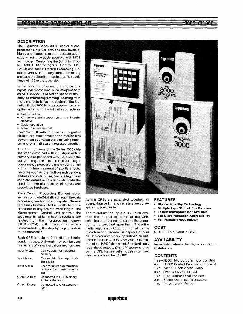
DE'lailE '5 DEVELBrUEflT KIT
DESCRIPTION The Signetics Series 3000 Bipolar Microprocessor Chip Set provides new levels of high performance to microprocessor applications not previously possible with MOS technology. Combining the Schottky bipolar N3001 Microprogram Control Unit (MCU) and N3002 Central Processing Element (CPE) with industry standard memory and support circuits, microinstruction cycle times of 100ns are possible.
In the majority of cases, the choice of a bipolar microprocessor slice, as opposed to an MOS device, is based on speed or flexibility of microprogramming. Starting with these characteristics, the design of the Signetics Series 3000 Microprocessor has been optimized around the following objectives:
• Fast cycle time • All memory and support chips are industry
standard • Cooler operation • Lower total system cost
Systems built with large-scale integrated circuits are much smaller and require less power than equivalent systems using medium and/or small scale integrated circuits.
The 2 components of the Series 3000 chip set, when combined with industry standard memory and peripheral circuits, allows the design engineer to construct highperformance processors and/or controllers with a minimum amount of auxiliary logic. Features such as the multiple independent address and data buses, tri-state logic, and separate output enable lines eliminate the need for time-multiplexing of buses and associated hardware.
Each Central Processing Element represents a complete 2-bit slice through the data processing section of a computer. Several CPEs may be connected in parallel to form a processor of any desired word length. The Microprogram Control Unit controls the sequence in which microinstructions are fetched from the microprogram memory (ROM/PROM), with these microinstructions controlling the step-by-step operation of the processor.
Each CPE contains a 2-bit slice of 5 independent buses. Although they can be used in a variety of ways, typical connections are:
Input M-bus:
Input I-bus:
Input K-bus:
Carries data from external memory
Carries data from input/output device
Used for microprogram mask or literal (constant) value in-put
Output A-bus: Connected to CPE Memory Address Register
Output O-bus: Connected to CPE accumu-lator.
40
As the CPEs are paralleled together, all buses, data paths, and registers are correspondinglyexpanded.
The microfunction input bus (F-bus) controls the internal operation of the CPE, selecting both the operands and the operation to be executed upon them. The arithmetic logic unit (ALU), controlled by the microfunction decoder, is capable of over 40 Boolean and binary operations as outlined in the FUNCTION DESCRIPTION section of the N3002 data sheet. Standard carry look-ahead outputs (X and Y) are generated by the CPE for use with industry standard devices such as the 74S182.
S!!IDOliCS
3'"111 M 1111011
FEATURES • Bipolar Schottky Technology • Multiple Input/Output Bus Structure • Fastest Microprocessor Available • 512 Microinstruction Addressibility • Full Function Accumulator
COST $100.00 (Total Value = $230)
AVAILABILITY Immediate delivery for Signetics Rep. or Distributors.
CONTENTS 1 ea-N3001 Microprogram Control Unit 4 ea-N3002 Central Processing Element 1 ea-74S182 Look-Ahead Carry 3 ea-82S114 256 x 8 PROM 1 ea-8T31 Bidirectional 110 Port 2 ea-8T26A Quad Bus Transceiver 1 ea-Introductory Manual
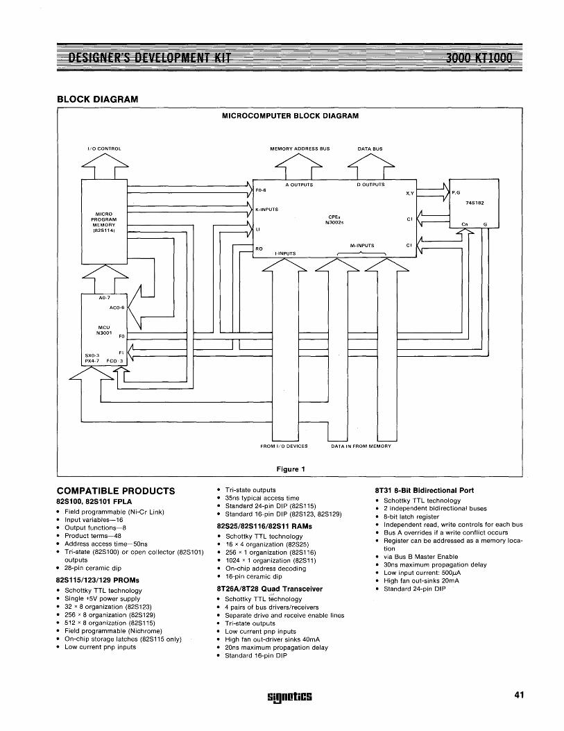
DESIGNER S DEvELQliMEN I KII BODf) KI1000
BLOCK DIAGRAM
MICROCOMPUTER BLOCK DIAGRAM
1/0 CONTROL
I---------------.. j) FO-6 V 1\
MEMORY ADDRESS BUS
A OUTPUTS
MICRO PROGRAM MEMORY (82S114)
I---------------.. j) K-INPUTS r
U .o7.CO , IC...-----J MCU I ~
N3001
SXO-3 PX4-7
FO~ ______ ~
A FI jlL-_____ ---!
FCO-3 ~
I---
.--__ ,j) LI
V r--
r--- RO I-INPUTS
CPEs N3002s
L
DATA BUS
D OUTPUTS
X.Y I----.. j) p.G
V 74S182
A CII" ___ ~
\f Cn G
M-INPUTS
A i ~ C I ~fl ... L.. _-_-_-_-_-_-_-_-....,-1
L---
FROM 1/0 DEVICES DATA IN FROM MEMORY
COMPATIBLE PRODUCTS 825100,825101 FPLA • Field programmable (Ni-Cr Link) • Input variables-16 • Output functions-8 • Product terms-48 • Address access time-50ns • Tri-state (82S100) or open collector (82S1 01)
outputs • 28-pin ceramic dip
825115/123/129 PROMs • Schottky TTL technology • Single +5V power supply • 32 x 8 organization (82S123) • 256 x 8 organization (82S129) • 512 x 8 organization (82S115) • Field programmable (Nichrome) • On-chip storage latches (82S115 only) • Low current pnp inputs
Figure 1
• Tri-state outputs 8T31 8-Bit Bidirectional Port • 35ns typical access time • Standard 24-pin DIP (82S115) • Standard 16-pin DIP (82S123, 82S129)
• Schottky TTL technology • 2 independent bidirectional buses • 8-bit latch register
82525/825116/82511 RAMs • Independent read, write controls for each bus
• Schottky TTL technology • 16 x 4 organization (82S25) • 256 x 1 organization (82S116) • 1024 x 1 organization (82S11) • On-chip address decoding • 16-pin ceramic dip
• Bus A overrides if a write conflict occurs • Register can be addressed as a memory loca-
tion • via Bus B Master Enable • 30ns maximum propagation delay • Low input current: 500jJ.A • High fan out-sinks 20mA
8T26A/8T28 Quad Transceiver • Standard 24-pin DIP
• Schottky TTL t~chnology • 4 pairs of bus drivers/receivers • Separate drive and receive enable lines • Tri-state outputs • Low current pnp inputs • High fan out-driver sinks 40mA • 20ns maximum propagation delay • Standard 16-pin DIP
Si!lDotiCS 41
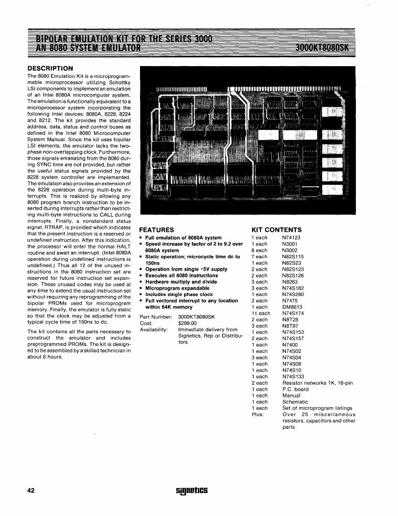
__ . _________________ ~ ~D_ E i-~ i3111;1! B I. P'li' R lE.tlEI.llo" III fAR t u r tell t 1M 211
AN 8080 SYSTEM Eulll'uliit
DESCRIPTION The 8080 Emulation Kit is a microprogrammabie microprocessor utilizing Schottky LSI components to implement an emulation of an Intel 8080A microcomputer system. The emulation is functionally equivalent to a microprocessor system incorporating the following Intel devices: 8080A, 8228, 8224 and 8212. The kit provides the standard address, data, status and control buses as defined in the Intel 8080 Microcomputer System Manual. Since the kit uses bipolar LSI elements, the emulator lacks the twophase non-overlapping clock. Furthermore, those signals emanating from the 8080 during SYNC time are not provided, but rather the useful status Signals provided by the 8228 system controller are implemented. The emulation also provides an extension of the 8228 operation during multi-byte interrupts. This is realized by allowing any 8080 program branch instruction to be inserted during interrupts ratherthan restricting multi-byte instructions to CALL during interrupts. Finally, a nonstandard status signal, RTRAP, is provided which indicates that the present instruction is a reserved or undefined instruction. After this indication the processor will enter the normal HALT routine and await an interrupt. (Intel 8080A operation during undefined instructions is undefined.) Thus all 12 of the unused instructions in the 8080 instruction set are reserved for future instruction set expansion. These unused codes may be used at any time to extend the usual instruction set without requiring any reprogramming of the bipolar PROMs used for microprogram memory. Finally, the emulator is fully static so that the clock may be adjusted from a typical cycle time of 150ns to dc.
The kit contains all the parts necessary to construct the emulator and includes preprogrammed PROMs. The kit is designed to be assembled by a skilled technician in about 8 hours.
42
FEATURES • Full emulation of 8080A system • Speed increase by factor of 2 to 9.2 over
8080A system • Static operation; microcycle time dc to
150ns • Operation from single +5V supply • Executes all 8080 instructions • Hardware multiply and divide • Microprogram expandable • Includes Single phase clock • Full vectored interrupt to any location
within 64K memory
Part Number: Cost: Avai labi I ity:
3000KT8080SK $299.00 Immediate delivery from Signetics, Rep or Distributors
S!!IDotiCG
KIT CONTENTS 1 each N74123 1 each N3001 8 each N3002 7 each N82S115 1 each N82S23 2 each N82S123 2 each N82S126 3 each N8263 3 each N74S182 1 each N74S280 2 each N7475 1 each DM8613 11 each N74S174 2 each N8T28 3 each N8T97 1 each N74S153 2 each N74S157 1 each N7400 1 each N74S02 3 each N74S04 1 each N74S08 1 each N74S10 1 each N74S133 2 each Resistor networks 1 K, 16-pin 1 each P.C. board 1 each Manual 1 each Schematic 1 each Set of microprogram listings Plus: Over 25 miscellaneous
resistors, capacitors and other parts
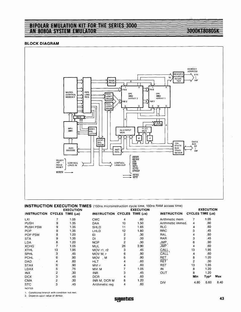
BLOCK DIAGRAM
MICRO· CONTROL MEMORY
MPU 3881
INST. DECODE
READY] INT I CONTROL HOLD LINES IN RESET [
~~~~ CONTROL ~ LINES OUT INTA
HLTA RTRAP
_HLDA _iNTI
A15
D0"
INSTRUCTION EXECUTION TIMES (150ns microinstruction cycle time, 150ns RAM access time) EXECUTION EXECUTION EXECUTION
INSTRUCTION CYCLES TIME (/-15) INSTRUCTION CYCLES TIME (/-15) INSTRUCTION CYCLES TIME (/-15)
LXI 7 1.05 CMC 4 .60 Arithmetic mem 7 1.05 PUSH 9 1.35 OAA 10 1.50 Arithmetic immed. 4 .60 PUSH PSW 9 1.35 SHLO 11 1.65 RLC 4 .60 POP 9 1.35 LHLO 12 1.80 RRC 3 .45 POP PSW 8 1.20 EI 2 .30 RAL 4 .60 STA 9 1.35 01 2 .30 RAR 3 .45 LOA 8 1.20 NOP 2 .30 JMP
--1 6 .90
XCHG 7 1.05 MUL 26 3.90 JMP 4 .60 XTHL 13 1.95 MOV r1, r2 3 .45 CALL 13 1.95 --, SPHL 3 .45 MOV M, r 6 .90 CALL 4 .60 PCHL 6 .90 MOV ,M 6 .90 RET 8 1.20 DAD 4 .60 HLT 4 .60 RET' 2 .30 STAX 6 .90 MVI r 4 .60 RST 13 1.95 LOAX 5 .75 MVIM 7 1.05 IN 8 1.20 INX 2 .30 INR 3 .45 OUT 8 1.20 OCX 3 .45 OCR 4 .60 Min Typ2 Max CMA 2 .30 INR M, OCR M 8 1.20
4.80 6.60 8.40 STC 3 .45 Arithmetic reg 4 .60
OIV
NOTES
1. Conditional branch with condition not met. 2. Depends upon value of divisor.
!ii!lDotiC!i 43
DESCRIPTION The Signetics Microassembler is a complete software package designed to support general slice system architectures which employ Signetics bipolar microprocessor components. It provides a flexible microassembly language required to describe the numerous configurations in which bipolar microprocessor chips are used. The program allows for the entry of specific device model parameters and hardware configurations which permits the symbolic assembly language to relate directly to the user's system. In particular, the microassembler provides primary support for the 3002 and 2901 central processing units and the 8X02 Control Store Sequencer through intrinsic field definitions for these devices. Through proper modification of the models used in the microassembler, it supports the 3001 Microprogram Control Unit as well as the 8X300 Fixed Instruction Bipolar Microprocessor.
In keeping with the varied nature of slice microprocessor systems, the microassembier provides for complete flexibility in adapting to the user's system definition. The microassembler provides for variable microinstruction formats as defined by the user. Moreover, op codes may be user-
44
defined. The following operators are supported by the microassembler:
A+B A"'-B -A A'B AlB
AMOD.B
A.SHL.B
ASHR.B .NOT.A AAND.B AOR.B
AXOR.B
Add A and B Add the complement of B to A Complement A Multiply A and B Compute the quotient of A divided by B Compute the remainder of A divided by B Shift A left B bits (supply zeroes to emptied bit positions) Shift A right B bits Invert all bits of A
,Logical and of bits in A and B Logical inclusive or of bits in A and B Logical exclusive or of bits in A and B
The microassembler itself is adaptable to convenient implementation by the user. The basic microassembler is written in standard ANSI FORTRAN IV. Therefore, the program may be run on virtually any machine of sufficient memory size which has the requisite FORTRAN compiler. Or, if desired, the program may be accessed via TYMSHARE, GE, or NCSS Timesharing Services.
Gi!)DotiCG
The outputs of the Signetics Microassembier will provide for complete system development and documentation. The microassembly program is a two-pass assembler. Upon assembly, a program listing is obtained which contains error messages relative to the success of the assembly process. This output is used in the debug stage of program development to produce code of the correct format. In the second pass, the complete program listing including source and object information directly provides the documentation required for the system firmware. A second output is also provided which is intended for the production of punched paper tape. The paper tape is deSigned for: 1) the production of PROMs which are to contain the object microprogram; 2) entry into ROM simulators for system checkout; and 3) entry into other microprocessor development systems.
CIIAPTER I BIPOlAR flHED InSTRUCTion
miCROPROCESSOR
Si!lDotiCS 45

46 !i!!lDotiC!i
INTRODUCTION
A Microcomputer Designed for Control
The 8X300 is a microcomputer designed for control. It features:
Execution Speed • 250ns instruction execution time • Direct address capability-up to 8192 16-bit
words of program memory • Eight 8-bit general purpose registers • Simultaneous data transfer and data edit in a
single instruction cycle time • n-way branch or n-entry table lookup in 2
instruction cycle times • 8X300 instructions operate with equal speed on
1-bit. 2-bit. 3-bit. 4-bit. 5-bit. 6-bit. 7-bit. or8-bit data formats
The 8X300 instruction set features controloriented instructions which directly access variable length input/output and internal data fields. These instructions provide very high performance for moving and interpreting data. This makes the 8X300 ideal in switching, controlling, and editing applications.
Direct Processing of External Data The 8X300 I/O system is treated as a set of internal registers. Therefore data from external devices may be processed (tested, shifted, added to, etc.) without first moving them to internal storage. I n fact, the enti re
concept is to treat data at the I/O interface no differently than internal data. This concept extends to the software which allows variables at the input/output system to be named and treated in the same way as data in storage.
Separate Program Storage and Data Storage The storage concept of the 8X300 is to separate program storage from data storage. Program storage is implemented in read-only memory in recognition of the fact that programs for control applications are fixed and dedicated. The benefits of using read-only memory are that great speeds may be obtained at lower cost than if read/write memory were used, and that program instructions reside in a nonvolatile medium and cannot be altered by system power failures.
8X300 Architecture Figure 2 of the 8X300 data sheet illustrates the 8X300 architecture. The 8X300 contains an Arithmetic Logic Unit (ALU), Program Counter, and an Address Register. Eight 8-bit general purpose registers are also pro-
Si!lDOliCS
vided, including 7 working registers and an auxiliary register which performs as a working register and also provides an implied operand for many instructions. The 8X300 registers are shown in Figure 2 of the 8X300 data sheet and are summarized below:
Control Registers include: • Instruction-A 16-bit register containing the
current instruction • Program Storage Address Register (AR)-A
13-bit register containing the address of the current instruction being accessed from Program Storage
• Program Counter (PC)-A 13-bit register containing the address of the next instruction to be read from Program Storage
Data Registers include: • Working Registers (WR)-Seven 8-bit registers
for data storage • Overflow (OVF)-A 1-bit register that retains
the most significant bit position carry from ALU addition operation. Arithmetically treated as 2°
• Auxiliary (AUX)-An 8-bit register. Source of implied operand for arithmetic and logical instructions. May be used as a working register.
A crystal external to the CPU may be used to generate the CPU system clock. The CPU executes 8 instruction types.
47
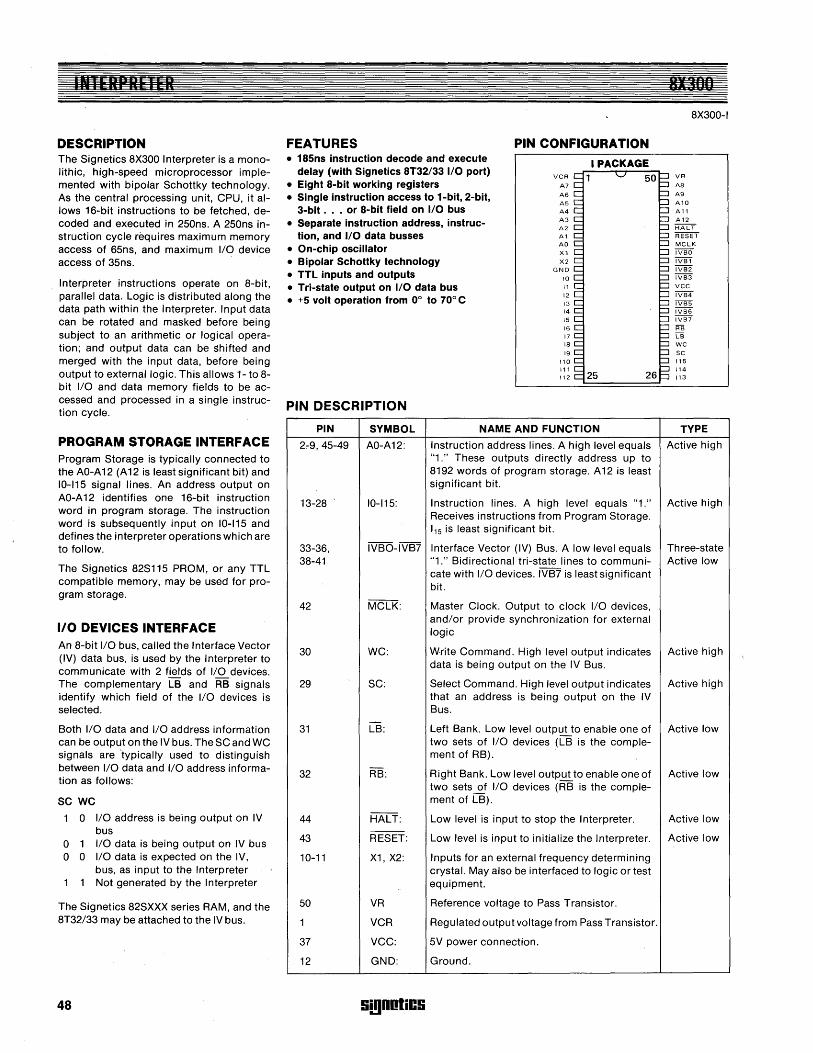
DESCRIPTION The Signetics 8X300 Interpreter is a monolithic, high-speed microprocessor implemented with bipolar Schottky technology. As the central processing unit, CPU, it allows 16-bit instructions to be fetched, decoded and executed in 250ns. A 250ns instruction cycle requires maximum memory access of 65ns, and maximum I/O device access of 35ns.
Interpreter instructions operate on 8-bit, parallel data. Logic is distributed along the data path within the Interpreter. Input data can be rotated and masked before being subject to an arithmetic. or logical operation; and output data can be shifted and merged with the input data, before being output to external logic. This allows 1- to 8-bit I/O and data memory fields to be accessed and processed in a single instruction cycle.
PROGRAM STORAGE INTERFACE Program Storage is typically connected to the AO-A12 (A12 is least significant bit) and 10-115 signal lines. An address output on AO-A 12 identifies one 16-bit instruction word in program storage. The instruction word is subsequently input on 10-115 and defines the interpreter operations which are to follow.
The Signetics 82S115 PROM, or any TTL compatible memory, may be used for program storage.
1/0 DEVICES INTERFACE An 8-bit I/O bus, called the I nterface Vector (IV) data bus, is used by the Interpreter to communicate with 2 fields of I/O devices. The complementary LB and RB signals identify which field of the 110 devices is selected.
Both I/O data and 110 address information can be output on the IV bus. The SC and WC signals are 'typically used to distinguish between I/O data and 110 address information as follows:
se we o I/O address is being output on IV
bus o 1 110 data is being output on IV bus o 0 I/O data is expected on the IV,
bus, as input to the Interpreter Not generated by the Interpreter
The Signetics 82SXXX series RAM, and the 8T32/33 may be attached to the IV bus.
48
FEATURES PIN CONFIGURATION • 185ns instruction decode and execute
delay (with Signetics 8T32/33 I/O port) VCR
I PACKAGE
• Eight 8-bit working registers A7 A6
A5
A4
A3
A2
Al AO Xl
X2
• Single instruction access to 1-bit, 2-bit, 3-bit . . . or 8-bit field on I/O bus
• Separate instruction address, instruc-tion, and I/O data busses
• On-chip oscillator • Bipolar Schottky technology • TTL inputs and outputs
GND
• Tri-state output on I/O data bus 10 11
12 13
14
15
16
17 18
19
• +5 volt operation from 0° to 70° C
PIN DESCRIPTION
PIN SYMBOL
2,..9,45-49 AO-A12:
13-28 10-115:
33-36, IVBO-IVB7 38-41
42 MCLK:
30 WC:
29 SC:
31 LB:
32 RB:
44 HALT: ---
43 RESET:
10-11 X1, X2:
50 VR
1 VCR
37 VCC:
12 GND:
!ii!lDotiC!i
110 111 112
NAME AND FUNCTION
Instruction address lines. A high level equals "1." These outputs directly address up to 8192 words of program storage. A12 is least Significant bit.
Instruction lines. A high level equals "1." Receives instructions from Program Storage. 115 is least significant bit.
Interface Vector (IV) Bus. A low level equals "1." Bidirectional tri-state lines to communi-cate with I/O devices. IVB7 is least significant bit.
Master Clock. Output to clock I/O devices, and/or provide synchronization for external logic
Write Command. High level output indicates data is being output on the IV Bus.
Select Command. High level output indicates that an address is being output on the IV Bus.
Left Bank. Low level output to enable one of two sets of I/O devices (LB is the comple-ment of RB).
Right Bank. Low level outp~ to enable one of two sets of I/O devices (RB is the comple-ment of LB).
Low level is input to stop the Interpreter.
Low level is input to initialize the Interpreter.
Inputs for an external frequency determining crystal. May also be interfaced to logic or test equipment.
Reference voltage to Pass Transistor.
Regulated output voltage from Pass Transistor.
5V power connection.
Ground.
BIllig
8X300-1
VR
A8
A9
Al0
All
A12
HALT RESET MCLK iVBO TVB1 'iVi32 iVB3 vcc iIIi34 i\iB5 iVB6 iVB7 As Ls wc SC
115 114 113
TYPE
Active high
Active high
Th ree-state Active low
Active high
Active high
Active low
Active low
Active low
Active low
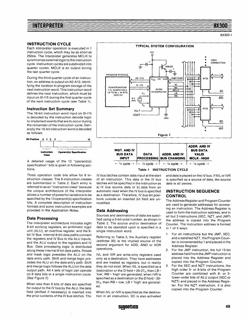
INTERPRETER
INSTRUCTION CYCLE Each interpreter operation is executed in 1 instruction cycle, which may be as short as 250ns. The Interpreter generates MCLK to synchronize external logic to the instruction cycle. Instruction cycles are subdivided into quarter cycles. MCLK is an output during the last quarter cycle.
During the third quarter cycle of an instruction, an address is output on AO-A 12, identifying the location in program storage of the next instruction word. This instruction word defines the next instruction, which must be input on 10-115 during the first quarter cycle of the next instruction cycle (see Table 1).
Instruction Set Summary The 16-bit instruction word input on 10-115 is decoded by the instruction decode logic to implement events that are to occur during the remainder of the instruction cycle. Generally the 16-bit instruction word is decoded as follows:
Bit POlition 0 1 2 3 15
I Inltruction Operand(l) Specification
CIa ..
A detailed usage of the 13 "operand (s) specification" bits is given in following sections.
Three operation code bits allow for 8 instruction classes. The 8 instruction classes are summarized in Table 2. Each entry is referred to as an "instruction class" because the unique architecture of the Interpreter allows a number of powerful variations to be specified by the 13 operand (s) specification bits. A complete description of instruction formats and some instruction examples are provided in the Application Notes.
Data Processing The Interpreter architecture includes eight 8-bit working registers, an arithmetic logic unit (ALU), an overflow register, and the 8-bit IV Bus. Internal8-bit data paths connect the registers and IV Bus to the ALU inputs, and the ALU output to the registers and IV Bus. Data processing logic is distributed along these internal 8-bit data paths. Rotate and mask logic precedes the ALU on the data entry path. Shift and merge logic precedes the ALU on the data entry path. Shift and merge logic follows the ALU on the data output path. All 4 sets of logic can operate on 8 data bits in a single instruction cycle. (See Figure 2)
When less than 8 bits of data are specified for output to the IV bus by the ALU, the data field (shifted if necessary) is inserted into the prior contents of the IV bus latches. The
81300 8X300-1
TYPICAL SYSTEM CONFIGURATION
+5V ()
• • r-1~
... ""
fF20 ~ PROGRAM STORAGE
• • ~
~
USER CONNECTION
A AO-A12 VCC VR VCR ~ IVBO-IVB7 r 8T32
f.-~
10-115 t.. ~ SC f.-
ROM/PROM/RAM WC ...... ~ f-TTL COMPATIBLE r 8X300 MCLK 1+ INTERPRETER f-UP TO 8k x 16 BITS X 1 LB
(82S115) RB ~ ~~z 0
-c..-. X2
HALT~ I 1 RESET
GND
f-r-
n ~
r f.--.-f--~
.... "',..
~
8T33
Tt • •
Figure 1
INST. AND IV BUS DATA
INPUT DATA ADDR.ANDIV
ADDR. AND IV BUS DATA
VALID MCLK=HIGH PROCESSING BUS CHANGING
+- 1/4 cycle -+ +- % cycle -+ +- 1/4 cycle -+ +- % cycle -+
Table 1 INSTRUCTION CYCLE
IV bus latches contain data input at the start of an instruction. This data in the IV bus latches will be specified in the instruction as a) IV bus source data or b) data from an automatic read when the IV bus is specified as a destination. Therefore, IV bus bit positions outside an inserted bit field are unmodified.
Dat{.l Addressing Sources and destinations of data are specified using a 5-bit octal number, as shown in Table 2. The source and/or destination of data to be operated upon is specified in a single instruction word.
Referring to Table 3, the Auxiliary register (address 00) is the implied source of the second argument for ADD, AND or XOR operations.
IVL and IVR are write-only registers used only as a destination. They have addresses and are treated as registers, but in reality they do not exist. When IVL is specified as a destination or the 0 field = 20-278, then LB = 'low', RB = 'high' are generated; when IVR is specified as a desti nation or the 0 field = 30-378, then RB = low, LB = 'high' are generated.
When IVL or IVR is specified as the destination in an instruction, SC is also activated
Si!lDotiCS
and data is placed on the IV bus. If IVL or IVR is specified as a source of data, the source data is all zeroes.
INSTRUCTION SEQUENCE CONTROL The Address Register and Program Counter are used to generate addresses for accessing an instruction. The Address Register is used to form the instruction address, and in all but 3 instructions (XEC, NZT, and JMP) the address is copied into the Program Counter. The instruction address is formed in 1 of 3 ways:
1. For all instructions but the JMP, XEC, and a satisfied NZT, the Program Counter is incremented by 1 and placed in the Address Register.
2. For the JMP instruction, the full 13-bit address field from the JMP instruction is placed into the Address Register and copied into the Program Counter.
3. For the XEC and NZT instructions, the high order 5- or 8-bits of the Program Counter are combined with 8- or 5-lower-order bits of ALU output (XEC or NZT) and placed in the Address Register. For the NZT instruction, it is also copied into the Program Counter.
49
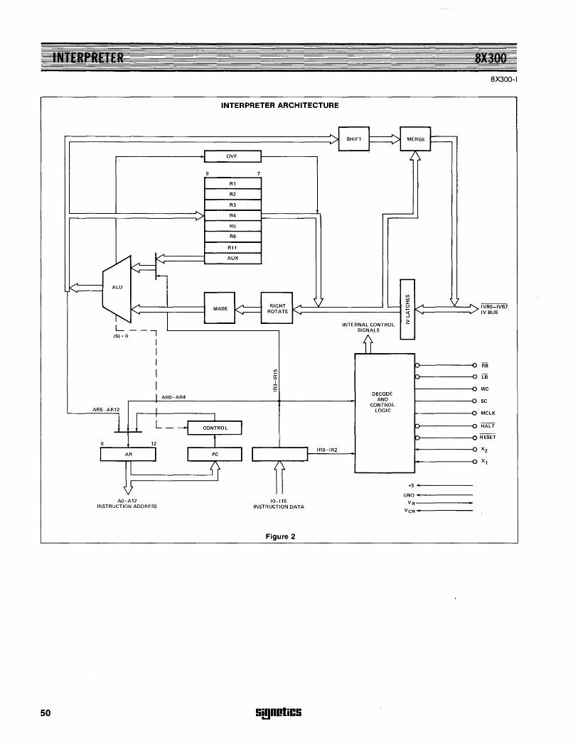
50
IF 'I R nEil It
.... K ...
/<=t ALU
~K L __
(S)=o I I I I I I I ARO-AR4
AR5-AR12 I
1 1 I
L_
0 12
I AR I
\1 AO-A12
INSTRUCTION ADDRESS
..
l
INTERPRETER ARCHITECTURE
J OVF I
0
Rl
R2
R3
':> R4
R5
R6
Rll
AUX
MASK K
I CONTROL I
1 PC J {r I
I
7
RIGHT .... K ROTATE ...
'" oc ~ £:
I. l.
10-115 INSTRUCTION DATA
Figure 2
!ii!lDotiC!i
~ V
I IRO-IR2
I
UXZlnO
8X300-1
L Joo. I SHIFT [ :>I MERGE r--
J ...
'---
INTERNAL CONTROL SIGNALS
fr
DECODE AND
CONTROL LOGIC
/\ L. l.
-~ 7 :r ..... V ... () f-
:3 ~
-I,.,.
I"" -I,.,. ~
I""
~ -,...
,...
" ,...
~ -.... ...., "" .... ....
+5 •
GND •
VR------------.
VCR~I~-----------
IVBO-IVB7 IV BUS
RB
LB
WC
SC
MCLK
HALT
RESET
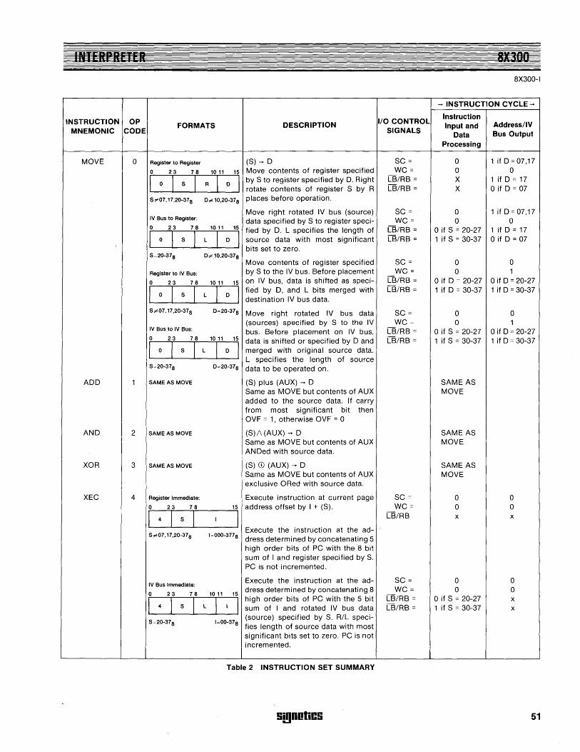
INTERPRETER
INSTRUCTION MNEMONIC
MOVE
ADD
AND
XOR
XEC
OP CODE
o
2
3
4
FORMATS
Register to Register
o 23 78 101115
I 0 I SiR I 0 I S;o!07,17,20-378 O;o! 10,20-378
IV Bus to Register:
o 2 3 7 8 10 11 15
O;o! 10,20-378
Register to IV Bus:
o 23 78 101115
I 0 I s I L I 0 I S;o!07,17,20-378 0=20-378
IV Bus to IV Bus:
r 0 '( s 'I L 10r 0 151
0=20-378
SAME AS MOVE
SAME AS MOVE
SAME AS MOVE
DESCRIPTION
(S) - D Move contents of register specified by S to register specified by D. Right rotate contents of register S by R places before operation.
Move right rotated IV bus (source) data specified by S to register specified by D. L specifies the length of source data with most significant bits set to zero.
Move contents of register specified by S to the IV bus. Before placement on IV bus, data is shifted as specified by D, and L bits merged with destination IV bus data.
Move right rotated IV bus data (sources) specified by S to the IV bus. Before placement on IV bus, data is shifted or specified by D and merged with original source data. L specifies the length of source data to be operated on.
(S) plus (AU X) - D Same as MOVE but contents of AUX added to the source data. If carry from most significant bit then OVF = 1, otherwise OVF = 0
(S)/\ (AUX) - D Same as MOVE but contents of AUX ANDed with source data.
(S) G> (AU X) - D Same as MOVE but contents of AUX exclusive ORed with source data.
Register Immediate: Execute instruction at current page r-0_-=,2r=-3 __ 7~8 ___ ~15 address offset by I + (S).
I 4 I s I I I S,..07,17,20-378
IV Bus Immediate:
0 23 78
I 4 I s I L
S=20-378
Execute the instruction at the ad-1=000-3778 dress determined by concatenating 5
1011 15
I I I 1=00-378
high order bits of PC with the 8 bit sum of I and register specified by S. PC is not incremented.
Execute the instruction at the address determined by concatenating 8 high order bits of PC with the 5 bit sum of I and rotated IV bus data (source) specified by S. R/L specifies length of source data with most significant bits set to zero. PC is not incremented.
Table 2 INSTRUCTION SET SUMMARY
!itgDotiC!i
I/O CONTROL SIGNALS
SC = WC=
LB/RB = LB/RB =
SC = WC =
LB/RB = LB/RB =
SC =
WC =
LB/RB = LB/RB =
SC = WC =
LB/RB = LB/RB =
SC = WC =
LB/RB
SC =
WC= LB/RB = LB/RB =
8X300
8X300-1
- INSTRUCTION CYCLE -
Instruction Input and
Data ProceSSing
o o X X
o o
o if S = 20-27 1 if S = 30-37
o o
Address/IV Bus Output
1 if D = 07,17 o
1 if D = 17 o if D = 07
1ifD=07,17 o
1 if D = 17 o if D = 07
o 1
o if D = 20-27 0 if D = 20-27 1 if D = 30-37 1 if D = 30-37
o o
o if S = 20-27 1 if S = 30-37
SAME AS MOVE
SAME AS MOVE
SAME AS MOVE
o o x
o o
o if S = 20-27 1 if S = 30-37
o 1
o if D = 20-27 1 if D = 30-37
o o x
o o x x
51
I PI' it
INSTRUCTION OP MNEMONIC CODE
NZT 5
XMIT 6
JMP 7
NOTE 1. RB is complement of LB. 2. "0" = Low voltage
"1" = High voltage x = Don't care
52
8Ml'n.
8X300-1
+- INSTRUCTION CYCLE ....
I/O CONTROL Instruction
FORMATS DESCRIPTION Input and Address/IV SIGNALS Data Bus Output
Processing
Register Immediate: If (S) = 0, jump to current page ad- SC = 0 0 0 23 78 15 dress offset by I; if S = 0, PC + 1 .... WC= 0 0
I 5 I s I I I PC LB/RB = x x If contents of register specified by S
S~07.17.20-378 1=000-3778 is non zero then transfer to address determined by concatenating 5 high order bits of PC with I; if contents of register specified by S is zero, incre-ment PC.
IV Bus Immediate: If right rotated IV bus data (source) SC = 0 0 0 23 78 1011 15 is Non Zero then Transfer to address WC= 0 0
I 5 I s I L I I I determined by concatenating 8 high CB/RB = o if S = 20-27 x order bits of PC with I; if contents of CB/RB = 1 if S = 30-37 X
S=20-378 1=00-378 register specified by S is zero, incre-ment PC.
Register Immediate:
0 23 78 15 Transmit I .... 0 SC = 0 1 if 0 = 07,17
I 6 I p I I ] Transmit and store 8 bit binary pat- WC= 0 0 tern I to register specified by D. LB/RB = x 1 if 0 = 17
D 110, 20-378 1=000-3778 CB/RD = x o if 0 = 07
IV BUS IMMEDIATE
0 23 78 1011 15 Transmit binary pattern I to IV bus. SC = 0 0
I 6 I 0 I L I I I Before placement on IV bus, literal WC= 0 1 I is shifted as specified by 0 and L LB/RB = o if 0 = 20-27 o if 0 = 20-27
0=20-378 1=00-378 bits merged with existing IV bus data. LB/RB = 1 if 0 = 30-37 1 if 0 = 30-37
Address Immediate:
0 23 15 Jump to Program Address A SC = 0 0
I 7 I A I Jump to program storage address WC= 0 0 A. A is stored in the address register LB/RB = x x
A = 00000-177778 (AR).
Table 2 INSTRUCTION SET SUMMARY (Cont'd)
INTERPRETER PACKAGE DIMENSIONS
I ~ 2.50 "\- 3° TO 7° ~ I- 25 "ADS .100 CENHRn .. , -----==i I ." ~
[:::::::::::::::::::::] ~ .07_1~ .15~ ~
Wi] Iron .018 TYP.-I~ .13
SmDHtiCS
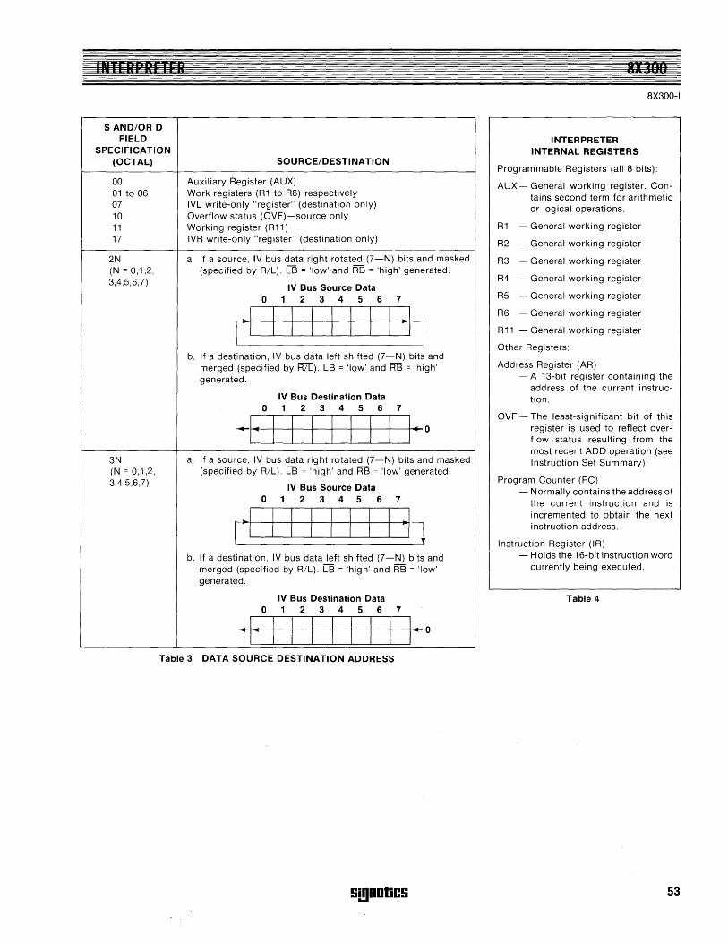
INTERPRETER
SAND/OR D FIELD
SPECIFICATION (OCTAL) SOURCE/DESTINATION
00 Auxiliary Register (AUX) 01 to 06 Work registers (R1 to R6) respectively 07 IVL write-only "register" (destination only) 10 Overflow status (OVF)-source only 11 Working register (R11) 17 IVR write-only "register" (destination only)
2N a. If a source, IV bus data right rotated (7-N) bits and masked (N = 0,1,2, (specified by R/L). LB = 'low' and RB = 'high' generated. 3,4,5,6,7)
IV Bus Source Data 0 1 2 3 4 5 6 7
cI I I I I I I I -Il b. If a destination, IV bus data left shifted (7-N) bits and
merged (specified by R/L). LB = 'low' and RB = 'high' generated.
IV Bus Destination Data 0 1 2 3 4 5 6 7
-I • I I I I I I I I· 0
3N a. If a source, IV bus data right rotated (7-N) bits and masked (N = 0,1,2, (specified by R/L). LB = 'high' and RB = 'low' generated. 3,4,5,6,7) IV Bus Source Data
0 1 2 3 4 5 6 7
rI I I I I I I I -I] b. If a destination, IV bus data left shifted (7-N) bits and
merged (specified by R/L). LB = 'high' and RB = 'low' generated.
IV Bus Destination Data 0 1 2 3 4 5 6 7
-I' I I I I I I I I· 0
Table 3 DATA SOURCE DESTINATION ADDRESS
S!!Inotics
aXlIIO
INTERPRETER INTERNAL REGISTERS
8X300-1
Programmable Registers (all 8 bits):
AUX - General working register. Contains second term for arithmetic or logical operations.
R1 - General working register
R2 - General working register
R3 - General working register
R4 - General working register
R5 - General working register
R6 - General working register
R11 - General working register
Other Registers:
Address Register (AR) - A 13-bit register containing the
address of the current instruction.
OVF - The least-significant bit of this register is used to reflect overflow status resulting from the most recent ADD operation (see Instruction Set Summary).
Program Counter (PC) - Normally contains the address of
the current instruction and is incremented to obtain the next instruction address.
Instruction Register (IR) - Holds the 16-bit instruction word
currently being executed.
Table 4
53
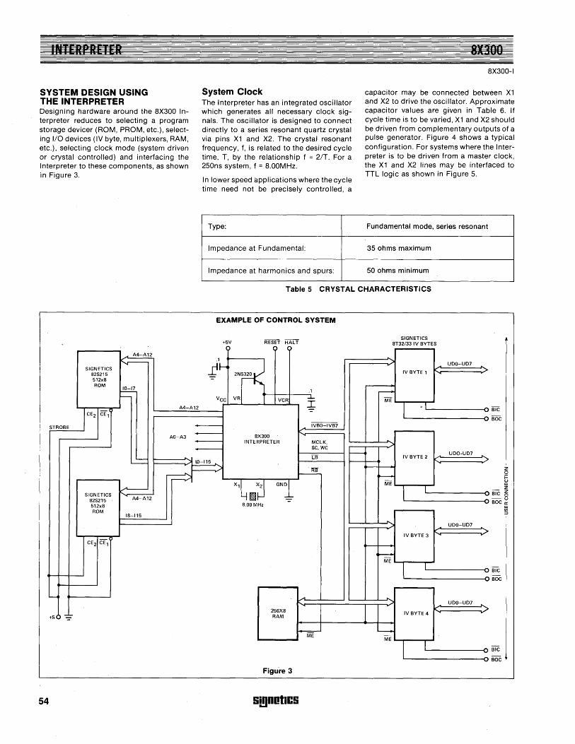
INTERDR' II R
SYSTEM DESIGN USING THE INTERPRETER Designing hardware around the 8X300 Interpreter reduces to selecting a program storage devicer (ROM, PROM, etc.), selecting I/O devices (IV byte, multiplexers, RAM, etc.), selecting clock mode (system driven or crystal controlled) and interfacing the Interpreter to these components, as shown in Figure 3.
..... A4-A12
....... SIGNETICS
82S215 512x8 ROM
110- 17
f--
A4-A12 -CE2 CE 1
STROBE
AO-A3
~ID -"- r
~ .A.
SIGNETICS A4-A12 82S215
512x8 ROM
18-115
CE2 CE 1
---<
+50 -==
54
System Clock The Interpreter has an integrated oscillator which generates all necessary clock signals. The oscillator is designed to connect directly to a series resonant quartz crystal via pins X1 and X2. The crystal resonant frequency, f, is related to the desired cycle time, T, by the relationship f = 2/T. For a 250ns system, f = 8.00MHz.
In lower speed applications where the cycle time need not be precisely controlled, a
Type:
Impedance at Fundamental:
Impedance at harmonics and spurs:
8X 11.0
8X300-1
capacitor may be connected between X1 and X2 to drive the oscillator. Approximate capacitor values are given in Table 6. If cycle time is to be varied, X1 and X2 should be driven from complementary outputs of a pulse generator. Figure 4 shows a typical configuration. For systems where the Interpreter is to be driven from a master clock, the X1 and X2 lines may be interfaced to TTL logic as shown in Figure 5.
Fundamental mode, series resonant
35 ohms maximum
50 ohms minimum
Table 5 CRYSTAL CHARACTERISTICS
EXAMPLE OF CONTROL SYSTEM
+5V RESET HALT ) 0 C)
.1
t~
'J~~ .1
V CC VR T ..l.. VCR
I
IVBO-IVB7
8X300 INTERPRETER MCLK,
SC, WC
LB ~
115 ......,
I RB ,...
Xl~~~ GNI
8.00 MHz
A
256X8 RAM
--=---" ME
Figu're 3
Si!lnDtics
SIGNETICS 8T32/33 IV BYTES
IV BYTE 1
r--ME
l .1
IV BYTE 2
~
ME
l I
" IV BYTE 3
~ ME
l 1
...
IV BYTE 4
--ME
I I
UDO-UD7
UDO-UD7
UDO-UD7
UDO-UD7
>
.... ~ ....
;>
.... ~ ....
;>
~ .... ~
""
... >
.... ....
BIC
BOC
BIC
BOC
BIC
BOC
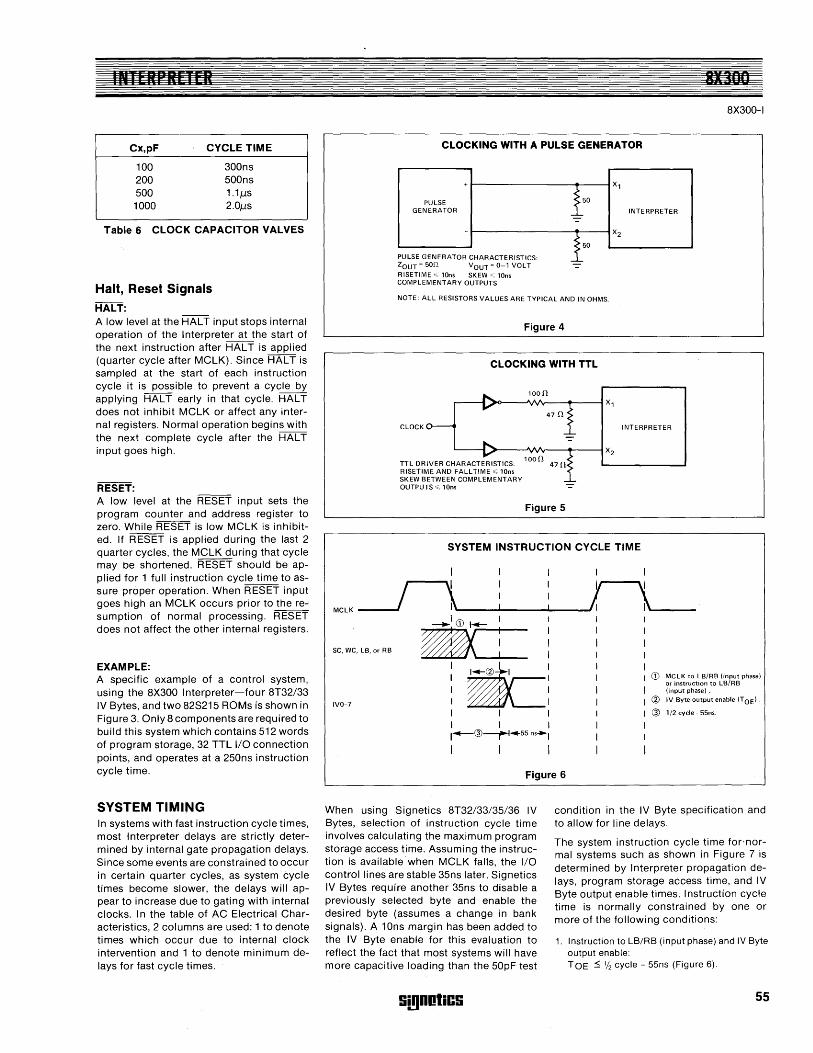
IN I LRPRETER
Cx,pF CYCLE TIME
100 300ns 200 500ns 500 1.1J,1s 1000 2.0J,1s
Table 6 CLOCK CAPACITOR VALVES
Halt, Reset Signals HALT: A low level at the HALT input stops internal operation of the Interpreter at the start of the next instruction after HALT is applied (quarter cycle after MCLK). Since HALT is sampled at the start of each instruction cycle it is possible to prevent a cycle by applying HALT early in that cycle. HALT does not inhibit MCLK or affect any internal registers. Normal operation begins with the next complete cycle after the HALT input goes high.
RESET: A low level at the RESET input sets the program counter and address register to zero. While RESET is low MCLK is inhibited. If RESET is applied during the last 2 quarter cycles, the MCLK during that cycle may be shortened. RESET should be applied for 1 full instruction cycle time to assure proper operation. When RESET input goes high an MCLK occurs prior to the resumption of normal processing. RESET does not affect the other internal registers.
EXAMPLE: A specific example of a control system, using the 8X300 Interpreter-four 8T32/33 IV Bytes, and two 82S215 ROMs is shown in Figure 3. Only 8 components are required to build this system which contains 512 words of program storage, 32 TTL I/O connection points, and operates at a 250ns instruction cycle time.
SYSTEM TIMING In systems with fast instruction cycle times, most I nterpreter delays are strictly determined by internal gate propagation delays. Since some events are constrained to occur in certain quarter cycles, as system cycle times become slower, the delays will appear to increase due to gating with internal clocks. In the table of AC Electrical Characteristics, 2 columns are used: 1 to denote times which occur due to internal clock intervention and 1 to denote minimum delays for fast cycle times.
BIlOQ
aX300-1
CLOCKING WITH A PULSE GENERATOR
+ X 1
1~ PULSE GENERATOR INTERPRETER
- -'"' X2
i~ PULSE GENERATOR CHARACTERISTICS: ZOUT = 50D. VOUT = 0-1 VOLT -RISETIME': 10ns SKEW <: 10ns COMPLEMENTARY OUTPUTS
NOTE: ALL RESISTORS VALUES ARE TYPICAL AND IN OHMS.
Figure 4
CLOCKING WITH TTL
>O--'V'v"v---+-----i X 1
CLOCK INTERPRETER
~--~~-~-~X2
TTL DRIVER CHARACTERISTICS: 100n RISETIME AND FALL TIME < 10ns SKEW BETWEEN COMPLEMENTARY OUTPUTS < 10ns -=-
Figure 5
SYSTEM INSTRUCTION CYCLE TIME
I I
MCLK __ -.II \~----~--------~~~-----SC, WC, LB, or RB
IVO-7
-,--.. :--1-= I
I I I 1~@~·55ns"'l
I I I
G) MCLK to LB/RB (input phase) or instruction to LB/RB (input phase) .
~ IV Byte output enable (TOE) .
@ 1/2 cycle· 55ns.
Figure 6
When using Signetics aT32/33/35/36 IV Bytes, selection of instruction cycle time involves calculating the maximum program storage access time. Assuming the instruction is available when MCLK falls, the I/O control lines are stable 35ns later. Signetics IV Bytes require another 35ns to disable a previously selected byte and enable the desired byte (assumes a change in bank signals). A 10ns margin has been added to the IV Byte enable for this evaluation to reflect the fact that most systems will have more capacitive loading than the 50pF test
SmootiCS
condition in the IV Byte specification and to allow for line delays.
The system instruction cycle time for·normal systems such as shown in Figure 7 is determined by Interpreter propagation delays, program storage access time, and IV Byte output enable times. Instruction cycle time is normally constrained by one or more of the following conditions:
1. Instruction to LB/RB (input phase) and IV Byte output enable: T OE ~ % cycle - 55ns (Figure 6).
55
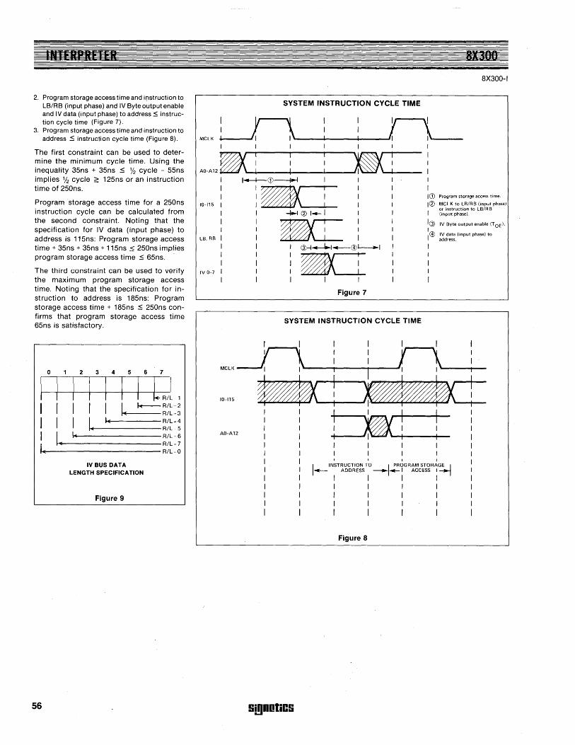
I'll R REIFR
2. Program storage access time and instruction to LB/RB (input phase) and IV Byte output enable and IV data (input phase) to address ~ instruction cycle time (Figure 7).
3. Program storage access time and instruction to address ~ instruction cycle time (Figure 8).
The first constraint can be used to determine the minimum cycle time. Using the inequality 35ns + 35ns ~ % cycle - 55ns implies 112 cycle;:: 125ns or an instruction time of 250ns.
Program storage access time for a 250ns instruction cycle can be calculated from the second constraint. Noting that the specification for IV data (input phase) to address is 115ns: Program storage access time + 35ns + 35ns + 115ns:$ 250ns implies program storage access time ~ 65ns.
The third constraint can be used to verify the maximum program storage access time. Noting that the specification for instruction to address is 185ns: Program storage access time + 185ns ~ 250ns confirms that program storage access time 65ns is satisfactory.
o 2 3 4 5 6 7
1111111 LL I I I I I I ~R/L~2
.... R/L ~3
I I I ~1. __ lo( _____ :~~:: I I ""1 .. .----------R/L~6
I ~ ... R/L~7 ....... ,.....------------- R/L~ 0
56
IV BUS DATA LENGTH SPECIFICATION
Figure 9
SYSTEM INSTRUCTION CYCLE TIME
Figure 7
SYSTEM INSTRUCTION CYCLE TIME
I
I
81300
8X300-1
ICD Program storage access time.
1<Ii MCLK to LB/RB (input phase) or instruction to LB/R B
I (input phase).
Ia> IV Byte output enable (T OEI. I I @ !~d~:!~. (input phase) to
--..... ' --..... ' MCLK~II \I_~.......--I _, \~ I I I
10-115 _~! w.x-+--AO-A12 !~! !
I I
I INSTRUCTION TO I PROGRAM STORAGE I -.- ADDRESS ---....- I ACCESS I .....
I I I I I I I I I I I I
I I I I , I I ,
Figure 8
Si!lDotiCS
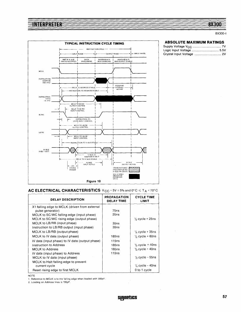
INTERPRETER
TYPICAL INSTRUCTION CYCLE TIMING
I INSTRUCTION CYCLE ·1 :_,NPUT,PHASE __ I_OUTPUT PHASE---:_INPUT PHASE
I INST& IV BUS II OATA AOORESS& IV I AOORESS& IV I I INPUTS ACCEPTEO PROCESSING BUS CHANGING I BUS OUTPUT STABLIE I I ., I 1 I I
MCLK ~ i Y \ 1 I I 1"----
i 1~! : INSTRUCTION ADDRESS IAO-A121
I I I RPROGRAM II I-----MCLK"(O ADDRESS STABL~--- S~~~:~SE---y
I I_'NSTRUCTIONTOADDRESSST~BLE-- 1 1
I I I 1 I INSTRUCTION --:'X ! __
(lo~~i~ -----+' ,'--___ .;..! ___ ~/I~'L__ -+"--- MCLK TO SC/WC II I
1 OUTPUT CONTROL _I 1"-- MCLK;O SC/WC I
__ -1-1--. INPUT CONTROL I 1 ~ I I / 1 \ I I .
SC/WC
---t-I 1- INSTRUCTION TO I LB/RB INPUT CONTROL
1 __ --- MCLK TO LB/RB -~--I' --1-: -..JX OUTPr CONTROL X~------';""---'X=
-----'1 1- MCLK TO LB/RB LB/RB
I INPU,T CONTROL 1 I
IV BUS I IVSO-IVB7)
I 1---INSTRu6T1oN TO IV BUS STA~LE III 1 I 1 1
i ~i l ~}-----+---------~ 1 \j - IV BUS TO -----.l I ~ ADDRESS STABLE I 1
I-----MCLK TO IV BUSSTABLE I
~ I_' IV BUS ----TI 1- IV BUS --
I INPUT ACTIVE OUTPUT ACTIVE
I/O----+-DEVICE CROSS HATCHED ~ ACCESS AREA INDICATES
Figure 10
IV BUS TRISTATE SOLID AREA INDICATES CHANGING DATA -
AC ELECTRICAL CHARACTERISTICS vcc = 5V ± 5% and O°C ~ T A < 70°C
DELAY DESCRIPTION PROPAGATION CYCLE TIME
DELAY TIME LIMIT
X1 falling edge to MCLK (driven from external pulse generator) 75ns
MCLK to SC/WC falling edge (input phase) 25ns
MCLK to SC/WC rising edge (output phase) % cycle + 25ns
MCLK to LB/RB (input phase) 35ns Instruction to LB/RB output (input phase) 35ns
MCLK to LB/RB (output phase) % cycle + 35ns
MCLK to IV data (output phase) 185ns % cycle + 60ns
IV data (input phase) to IV data (output phase) 115ns Instruction to Address 185ns Y2 cycle + 40ns
MCLK to Address 185ns % cycle + 40ns
IV data (input phase) to Address 115ns
MCLK to IV data (input phase) % cycle - 55ns
MCLK to Halt falling edge to prevent current cycle % cycle - 40ns
Reset rising edge to first MCLK o to 1 cycle
NOTE
1. Reference to MCLK is to the falling edge when loaded with 300pF.
2. Loading on Address lines is 150pF.
!ii!ln~tiC!i
81300 8X300-1
ABSOLUTE MAXIMUM RATINGS Supply Voltage VCC ................................. 7V LogiC Input Voltage ............................... 5.5V Crystal Input Voltage ............................... 2V
57
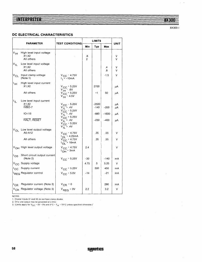
INTERPRETER 8X]00
8X300-1
DC ELECTRICAL CHARACTERISTICS
LIMITS PARAMETER TEST CONDITIONS UNIT
Min Typ Max
V'H High level input voltage X1,X2 .6 V All others 2 V
V ,L Low level input voltage X1,X2 .4 V All others .8 V
VCL Input clamp voltage V CC = 4.75V -1.5 V (Note 1) " = -10mA
"H High level input current X1,X2 V CC = 5.25V 2700 JJA
All others V ,H = .6V V CC = 5.25V <1 50 JJA V IH = 4.5V
',L Low level input current X1,X2 V CC = 5.25V -2500 JJA IVBO-7 V IL = .4V -140 -200 JJA
V cc = 5.25V 10-115 V ,L =.4V -880 -1600 JJA
HALT, RESET V CC = 5.25V V IL = .4V -230 -400 JJA V cc = 5.25V V IL = .4V
VOL Low level output voltage AO-A12 V CC = 4.75V .35 .55 V
All others I OL = 4.25mA V CC = 4.75V .35 .55 V 'OL = 16mA
VOH High level output voltage V CC = 4.75V 2.4 V 'OH = 3mA
'OS Short circuit output current (Note 2) V CC = 5.25V -30 -140 mA
VCC Supply voltage 4.75 5 5.25 V
ICC Supply current V CC = 5.25V 300 450 mA
I REG Regulator control V CC = 5.0V -14 -21 mA
'CR Regulator current (Note 3) VCR = 0 290 mA
VCR Regulator voltage (Note 3) V REG = OV 2.2 3.2 V
NOTES
1. Crystal inputs X1 and X2 do not have clamp diodes.
2. Only one output may be grounded at a time.
3. (Limits apply for VCC = 5V ± 5% and ODC < T A < 70DC unless specified otherwise.)"
58 Si!lnntics
MeeA' 81300 CROSS ASSEMBLER
DESCRIPTION The MicroControlier Cross Assembly Program (MCCAP) is a program designed to translate symbolic instructions into object code that can be executed by the 8X300. This program will run on most computers that have a Fortran compiler with a computer word length of at least 16 bits and a random access I/O capability; it can be run on most minicomputers as well as large scale computers.
The Assembler is written in Fortran. This provides compatibility with most computer systems and makes it transportable. The program is modular and uses a minimum of memory. However, it may be operated in an overlay mode if necessary.
FEATURES • 9 track EBCDIC tape • Cross Assembler (written in Fortran) • Flexible Object Format MCSIM
ROM Simulator ROM Production Format
• Symbolic Addressing • Forward References • Expression Evaluation • Symbolic I/O Representation
The Assembler is a two-pass program that issues helpful error messages and produces an easily read program listing. An object module may be loaded into the SMS MicroController Simulator (MCSIM), the SMS ROM Simulator 1000A, or used to produce ROMs or PROMs.
The Assembler features symbolic addressing, forward references and expression evaluation. It also has the capability to symbolically represent the Interface Vector (IV). In addition, the Assembler is capable of expressing data in several number systems as well as in ASCII character codes.
S!!)DotiCS
8X 31104 S 11 II IS S
MCCAP Output The output from a MCCAP compilation includes an assembler listing and an object module. During pass 2 of the assembly process, a program listing is produced. The listing displays ali information pertaining to the assembled program. This includes the assembled octal instructions, the user's original source code and error messages. The listing may be used as a documentation tool through the inclusion of comments and remarks which describe the function of a particular program segment. The main purpose of the listing, however, is to convey ali pertinent information about the assembled program, i.e., the memory addresses and their contents.
The object module is also produced during pass 2. This is a machine readable computer output produced on paper tape. The output module contains the specifications necessary for loading the memory of the SMS.*
Microcontrolier Simulator (MCSIM), for loading the memory of ROM Simulator, or for prodUCing ROMs or PROMs. The object module can be produced in MCSIM, ROM Simulator or BNPF format.
*Scientific Micro System 520 Clyde Avenue Mountain View, CA 94043
59
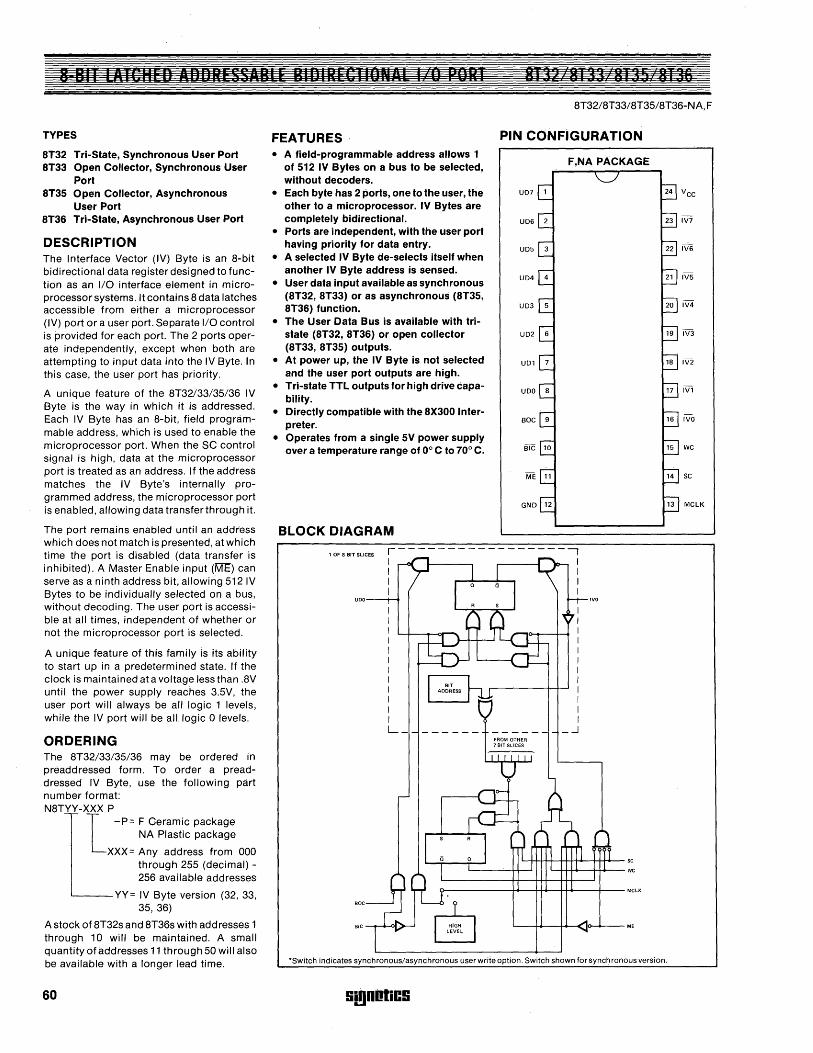
8 BIT EAICHPn AIJIJRFHSAH' F H'OIRFt:TIONl'l () PORT 8T12 81311 UT:l5 8136
TYPES
8T32 Tri-State, Synchronous User Port 8T33 Open Collector, SynchronoLis User
Port 8T3S Open Collector, Asynchronous
User Port 8T36 Tri-State, Asynchronous User Port
DESCRIPTION The Interface Vector (IV) Byte is an B-bit bidirectional data register designed to function as an I/O interface element in microprocessor systems. It contains B data latches accessible from either a microprocessor (IV) port or a user port. Separate I/O control is provided for each port. The 2 ports operate independently, except when both are attempting to input data into the IV Byte. In this case, the user port has priority.
A unique feature of the BT32/33/35/36 IV Byte is the way in which it is addressed. Each IV Byte has an B-bit, field programmable address, which is used to enable the microprocessor port. When the SO control signal is high, data at the microprocessor port is treated as an address. If the address matches the IV Byte's internally programmed address, the microprocessor port is enabled, allowing data transfer through it.
The port remains enabled until an address which does not match is presented, at which time the port is disabled (data transfer is inhibited). A Master Enable input (ME) can serve as a ninth address bit, allowing 5121V Bytes to be individually selected on a bus, without decoding. The user port is accessible at all times, independent of whether or not the microprocessor port is selected.
A unique feature of this family is its ability to start up in a predetermined state. If the clock is maintained at a voltage less than .BV until the power supply reaches 3.5V, the user port will always be all logic 1 levels, while the IV port will be all logic a levels.
ORDERING The BT32/33/35/36 may be ordered in preaddressed form. To order a preaddressed IV Byte, use the following part number format: NBTYY-XXX P T -P= F Ceramic package L NA Plastic package
XXX= Any address from 000 through 255 (decimal) -256 available addresses
'-----YY= IV Byte version (32, 33, 35,36)
A stock of BT32s and BT36s with addresses 1 through 10 will be maintained. A small quantity of addresses 11 through 50 will also be available with a longer lead time.
60
BT32/BT33/8T35/BT36-NA, F
FEATURES • A field-programmable address allows 1
of S12 IV Bytes on a bus to be selected, without decoders.
• Each byte has 2 ports, one to the user, the other to a microprocessor. IV Bytes are completely bidirectional.
• Ports are independent, with the user port having priority for data entry.
• A selected IV Byte de-selects itself when another IV Byte address is sensed.
• User data input available as synchronous (8T32, 8T33) or as asynchronous (8T3S, 8T36) function.
• The User Data Bus is available with tristate (8T32, 8T36) or open collector (8T33, 8T3S) outputs.
• At power up, the IV Byte is not selected and the user port outputs are high.
• Tri-state TTL outputs for high drive capability.
• Directly compatible with the 8X300 Interpreter.
• Operates from a single SV power supply over a temperature range of 0° C to 70° C.
BLOCK DIAGRAM
PIN CONFIGURATION
F,NA PACKAGE
UD7 1
UD6 2
UD5 3
UD4 4
UD3 5
UD2 6
UD1 7
UDO 8
BOC 9
BIC 10
ME 11
GND 12
, OF 8 BIT SLICES ,-----------------,
UDQ
BOC
I I I I
I I I I I I I I I I I I L_
I I I
_--.J
~++++-I-++++--Hf.f+- sc '-++-+-4-++'>---- wc
1;>------+~_+++-_++-4---+_- MCLK
ME
24
23
22
21
20
19
18
17
16
15
14
13
'Switch indicates synchronous/asynchronous user write option. Switch shown for synchronous version.
!ii!lDotiC!i
VCC
IV7
IV6
IV5
IV4
IV3
IV2
IV1
IVO
WC
SC
MCLK
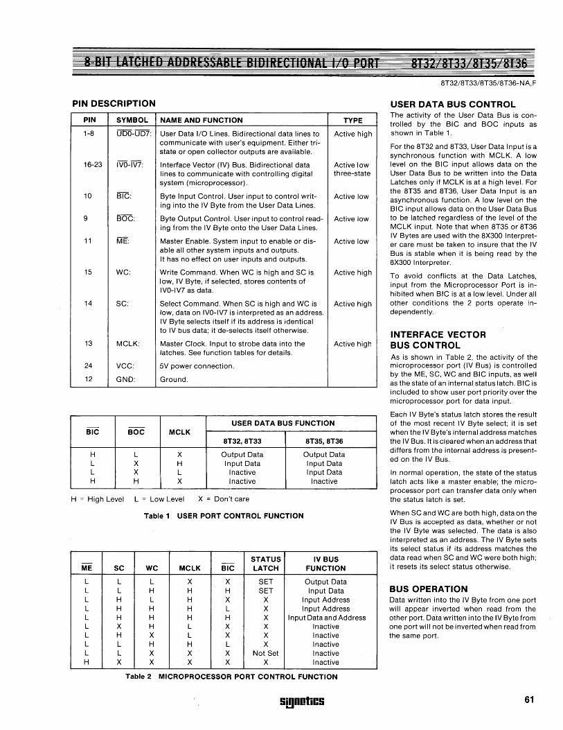
8 BIT LATCHED ADDRESSABLE BIDIRECIIONnL I 0 PORI
PIN DESCRIPTION
PIN SYMBOL NAME AND FUNCTION TYPE
1-8 UDO-UD?: User Data I/O Lines. Bidirectional data lines to Active high communicate with user's equipment. Either tri-state or open collector outputs are available.
16-23 IVO-IV?: Interface Vector (IV) Bus. Bidirectional data Active low lines to communicate with controlling digital th ree-state system (microprocessor).
10 BIC: Byte Input Control. User input to control writ- Active low ing into the IV Byte from the User Data Lines.
9 BOC: Byte Output Control. User input to control read- Active low ing from the IV Byte onto the User Data Lines.
11 ME: Master Enable. System input to enable or dis- Active low able all other system inputs and outputs. It has no effect on user inputs and outputs.
15 WC: Write Command. When WC is high and SC is Active high low, IV Byte, if selected, stores contents of IVO-IV? as data.
14 SC: Select Command. When SC is high and WC is Active high low, data on IVO-IV? is interpreted as an address. IV Byte selects itself if its address is identical to IV bus data; it de-selects itself otherwise.
13 MCLK: Master Clock. Input to strobe data into the Active high latches. See function tables for details.
24 VCC: 5V power connection.
12 GND: Ground.
USER DATA BUS FUNCTION - --BIC BOC MCLK
8T32,8T33 8T35,8T36
H L X Output Data Output Data L X H Input Data Input Data L X L Inactive Input Data H H X Inactive Inactive
H High Level L = Low Level X = Don't care
Table 1 USER PORT CONTROL FUNCTION
STATUS IV BUS - -ME SC WC MCLK BIC LATCH FUNCTION
L L L X X SET Output Data L L H H H SET Input Data L H L H X X Input Address L H H H L X Input Address L H H H H X Input Data and Address L X H L X X Inactive L H X L X X Inactive L L H H L X Inactive L L X X X Not Set Inactive H X X X X X Inactive
Table 2 MICROPROCESSOR PORT CONTROL FUNCTION
!ii!)DotiC!i
8132 8133 8135 8136 8T32/8T33/8T35/8T36-NA, F
USER DATA BUS CONTROL The activity of the User Data Bus is controlled by the BIC and BOC inputs as shown in Table 1.
For the 8T32 and 8T33, User Data Input is a synchronous function with MCLK. A low level on the BIC input allows data on the User Data Bus to be written into the Data Latches only if MCLK is at a high level. For the 8T35 and 8T36, User Data Input is an asynchronous function. A low level on the BIC input allows data on the User Data Bus to be latched regardless of the level of the MCLK input. Note that when 8T35 or 8T36 IV Bytes are used with the 8X300 Interpreter care must be taken to insure that the IV Bus is stable when it is being read by the 8X300 Interpreter.
To avoid conflicts at the Data Latches, input from the Microprocessor Port is inhibited when BIC is at a low level. Under all other conditions the 2 ports operate independently.
INTERFACE VECTOR BUS CONTROL As is shown in Table 2, the activity of the microprocessor port (IV Bus) is controlled by the ME, SC, WC and BIC inputs, as well as the state of an internal status latch. BIC is included to show user port priority over the microprocessor port for data input.
Each IV Byte's status latch stores the result of the most recent IV Byte select; it is set when the IV Byte's internal address matches the IV Bus. It is cleared when an address that differs from the internal address is presented on the IV Bus.
In normal operation, the state of the status latch acts like a master enable; the microprocessor port can transfer data only when the status latch is set.
When SC and WC are both high, data on the IV Bus is accepted as data, whether or not the IV Byte was selected. The data is also interpreted as an address. The IV Byte sets its select status if its address matches the data read when SC and WC were both high; it resets its select status otherwise.
BUS OPERATION Data written into the IV Byte from one port will appear inverted when read from the other port. Data written into the IV Byte from one port will not be inverted when read from the same port.
61
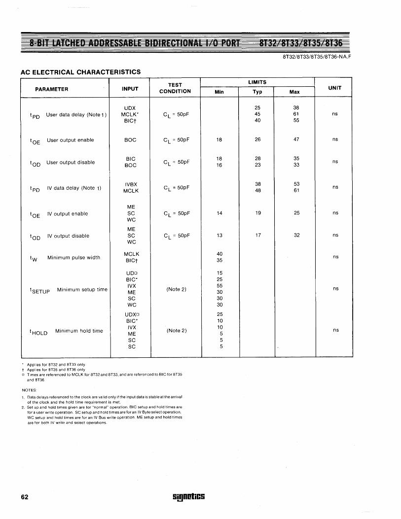
8 B' I LIITCHED ADDRESSABLE BIDIRECT DIAL I 0 PORT
AC ELECTRICAL CHARACTERISTICS
PARAMETER
tpD User data delay (Note 1 )
tOE User output enable
taD User output disable
tpD IV data delay (Note 1)
tOE IV output enable
taD IV output disable
tw Minimum pulse width
tSETUP Minimum setup time
t HOLD Minimum hold time
• Applies for 8T32 and 8T33 only. t Applies for 8T35 and 8T36 only.
INPUT
UDX MCLK* BICt
BOC
BIC BOC
IVBX MCLK
ME SC WC
ME SC WC
MCLK BICt
UDo BIC* IVX ME SC WC
UDXo BIC* IVX ME SC SC
TEST CONDITION
C L = 50pF
C L = 50pF
C L = 50pF
C L = 50pF
C L = 50pF
C L = 50pF
(Note 2)
(Note 2)
o Times are referenced to MCLK for 8T32 and 8T33. and are referenced to BIC for 8T35 and 8T36.
NOTES:
1. Data delays referenced to the clock are valid only if the input data is stable at the arrival of the clock and the hold time requirement is met.
2. Set up and hold times given are for "normal" operation. BIC setup and hold times are for a user write operation. SC setup and hold times are for an IV Byte select operation. WC setup and hold times are for an IV Bus write operation. ME setup and hold times are for both IV write and select operations.
62 !ii!)DotiC!i
Min
18
18 16
14
13
40 35
15 25 55 30 30 30
25 10 10 5 5 5
8T32 8T33 8135 BT3& 8T32/8T33/8T35/8T36-NA, F
LIMITS
Typ UNIT
Max
25 38 45 61 ns 40 55
26 47 ns
28 35 23 33
ns
38 53 48 61
ns
19 25 ns
17 32 ns
ns
ns
ns
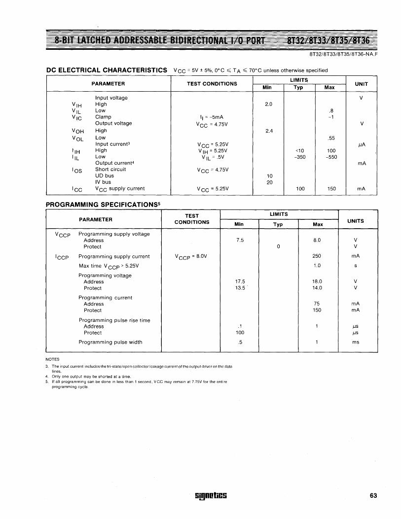
8 Bit LAIOnED ADDRESSABLE BIDIReCTIONAL I 0 PORT 8T32 8T33 8T35 8T3G ST32/ST33/ST35/ST36-NA. F
DC ELECTRICAL CHARACTERISTICS v cc = 5V ± 5%, OcC ~ T A ~ 70cC unless otherwise specified
PARAMETER TEST CONDITIONS
Input voltage
VIH High
VIL Low
VIC Clamp II = -5mA Output voltage VCC = 4.75V
VOH High
VOL Low Input current3 VCC = 5.25V
IIH High V IH = 5.25V IlL Low V IL = .5V
Output current4
lOS Short circuit VCC = 4.75V UD bus IV bus
ICC V CC supply current V CC = 5.25V
PROGRAMMING SPECIFICATIONS5
TEST PARAMETER CONDITIONS
VCCP Programming supply voltage Address Protect
ICCp Programming supply current VCCP = S.OV
Max time V CCP > 5.25V
Programming voltage Address Protect
Programming current Address Protect
Programming pulse rise time Address Protect
Programming pulse width
NOTES
3. The input current includes the tri-statelopen collector leakage current of the output driver on the data lines.
4. Only one output may be shorted at a time. 5. If all programming can be done in less than 1 second, vee may remain at 7.7SV for the entire
programming cycle.
S!!IDotiCS
Min
7.5
17.5 13.5
.1 100
.5
LIMITS Min Typ Max
2.0 .S -1
2.4 .55
<10 100 -350 -550
10 20
100 150
LIMITS
Typ Max
S.O 0
250
1.0
1S.0 14.0
75 150
1
1
UNIT
V
V
J.1A
mA
mA
UNITS
V V
mA
s
V V
mA mA
J.1s J.1S
ms
63
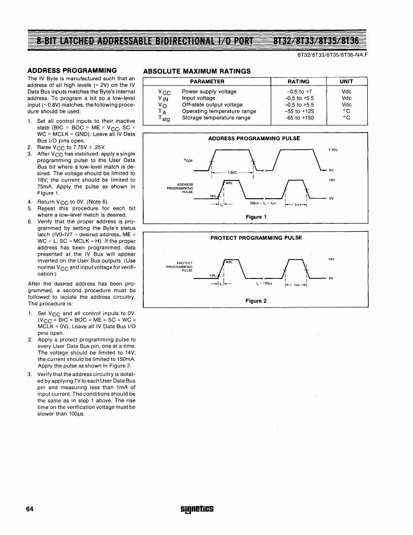
B BIT LATCHED /lDDRESSABLE BIDIRECTIONAL o PORT 8T32 BT33 BI35 BT36
ADDRESS PROGRAMMING The IV Byte is manufactured such that an address of all high levels (> 2V) on the IV Data Bus inputs matches the Byte's internal address. To program a bit so a low-level input « O.BV) matches, thefollowing procedure should be used:
1. Set all control inputs to their inactive state (BIC = BOC = ME = V CC, SC = WC = MCLK = GND). Leave all IV Data Bus I/O pins open.
2. Raise VCC to 7.75V ± .25V. ,3. After VCC has stabilized, apply a single
programming pulse to the User Data Bus bit where a low-level match is desired. The voltage should be limited to 1BV; the current should be limited to 75mA. Apply the pulse as shown in Figure 1.
4. Return VCC to OV. (Note 6). 5. Repeat this procedure for each bit
where a low-level match is desired. 6. Verify that the proper address is pro
grammed by setting the Byte's status latch (IVO-IV7 = desired address, ME = WC = L, SC = MCLK = H). If the proper address has been programmed, data presented at the IV Bus will appear inverted on the User Bus outputs. (Use normal V CC and input voltage for verification.)
After the desired address has been programmed, a second procedure must be followed to isolate the address circuitry. The procedure is:
1. Set VCC and all control inputs to OV. (VCC = BIC = BOC = ME = SC = WC = MCLK = OV). Leave all IV Data Bus I/O pins open.
2. Apply a protect programming pulse to every User Data Bus pin, one at a time. The voltage should be limited to 14V; the current should be limited to 150mA. Apply the pulse as shown in Figure 2.
3. Verify that the address circuitry is isolated by applyi ng 7V to each User Data Bus pin and measuring less than 1 mA of input current. The conditions should be the same as in step 1 above. The rise time on the verification voltage must be slower than 100l1s.
64
BT32/BT33/BT35/BT36-NA, F
ABSOLUTE MAXIMUM RATINGS
PARAMETER RATING UNIT
VCC Power supply voltage -0.5 to +7 Vdc VIN Input voltage -0.5 to +5.5 Vdc Vo Off-state output voltage -0.5 to +5.5 Vdc TA Operating temperature range -55 to +125 °C T stg Storage temperature range -65 to +150 °C
ADDRESS PROGRAMMING PULSE
~r-\7'75V
Vccp .
I I ov !-lSEC.---1
-1L1 1 JL18V ADDRESS 90%
PROGRAMMING I PULSE I
10% 1 I ov
L I I -I t, lOOns <"t, < l~s r--< lms-I
Figure 1
PROTECT PROGRAMMING PULSE
-1LJL14V
PROTECT 90% PROGRAMMING 1 I
PULSE
10% I 1 1
I 1 I ov
--I t, --- t, > 100~s 1--> lms-l
Figure 2
Si!)DotiCS
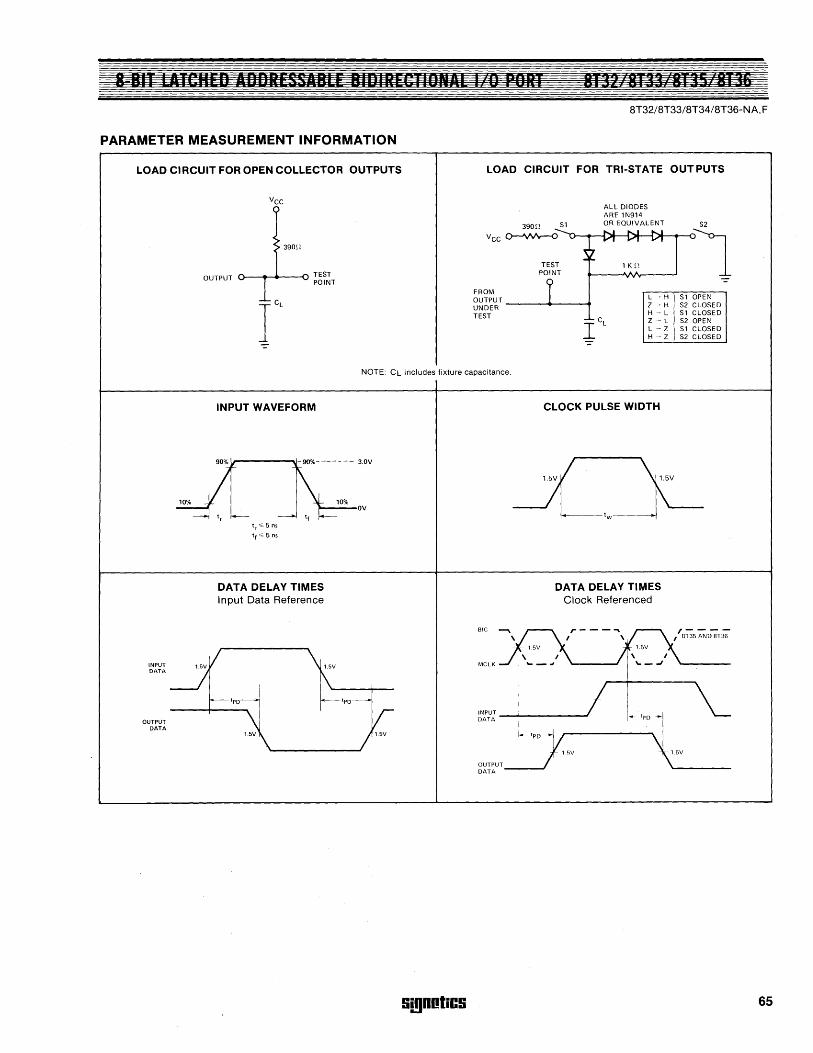
8 BIT LATEUED ADDRESSABLE BIDIRECTIBNIlL I B PBRT 8T32 8133 8135 IT36
BT32/BT33/BT34/BT36-NA, F
PARAMETER MEASUREMENT INFORMATION
LOAD CIRCUIT FOR OPEN COLLECTOR OUTPUTS LOAD CIRCUIT FOR TRI-STATE OUTPUTS
390n S1
V CC ()---J\/\/'y-O
FROM
TEST POINT
8~b~~T ---....... ---i TEST
ALL DIODES ARE 1N914 OR EQUIVALENT S2
1 K,1 1 L - H S1 OPEN Z - H S2 CLOSED H - L S1 CLOSED Z .- L S2 OPEN L - Z S1 CLOSED H· Z S2 CLOSED
NOTE: CL includes fixture capacitance.
INPUT DATA
OUTPUT DATA
INPUT WAVEFORM
DATA DELAY TIMES Input Data Reference
!ii!lDotiC!i
CLOCK PULSE WIDTH
DATA DELAY TIMES Clock Referenced
BIC
MCLK
~:~; __ ~ ________ -J
-- 'po ----II /'5V
g~i~uT __ --J
.- 'po ~I
\,-----.5V
65
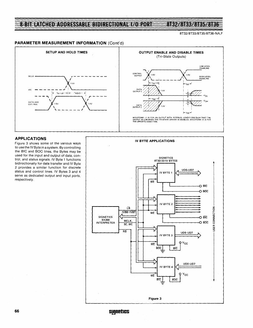
B BI1 [ATCHED ADDRESSIBI E BIDIRECTIQNAL I o PORT BT12 ST33 Blah 813& BT32/BT33/BT35/BT36-NA, F
PARAMETER MEASUREMENT INFORMATION (Cont'd)
SETUP AND HOLD TIMES
MCLK --------,. ,---------I
BIC
-- 'SETUP -- --- 'HOLD -'-
APPLICATIONS Figure 3 shows some of the various ways to use the IV Byte in a system. By controlling the BIC and BOC lines, the Bytes may be used for the input and output of data, control, and status signals. IV Byte 1 functions bidirectionally for data transfer and IV Byte 2 provides a similar function for discrete status and control lines. IV Bytes 3 and 4 serve as dedicated output and input ports, respectively.
[8
OUTPUT ENABLE AND DISABLE TIMES (Tri-State Outputs)
LOW LEVEL
CONTROL \ 1/ )( *r ____ ENABLING
OUTPUT 1.5V 1.5V
OATA OUTPUT 1
DATA OUTPUT 2
I \ 'I ~~~~t~NVGEL '--1-------' I "-----
L'OE---I /+tOD+1 I I I
I I
~~...:........<..~ ____ +I....;;;.:..~~- -VOL
WAVEFORM ul is FOR AN OUTPUT WiTH INTERNAL CONDITIONS SUCH THAT THE OUTPUT IS LOW WHEN THE TRI-STATE DRiVER IS ENABLED. WAVEFORM =2 is FOR THE OPPOSITE CONDITION.
IV BYTE APPLICATIONS
SIGNETICS 8T32/33 IV BYTES
~ < IV BYTE 1
r--M1:
I I
') .. V
IV BYTE 2
UDO-UD7 > -0
<)
~
IVBO-IVB7 ME SIGNETICS It I I -0
8X300 'f MCLK, ,... INTERPRETER
SC,WC t-- .....
BIC
BOC
~ RB UDO-UD7 ~ IV BYTE 3 V
~ ME VCC
BO~ BIC
-1) y
~ UDO-UD7
IV BYTE 4
ME VCC
mc-L BOC
Figure 3
66 Si!lDotiCS
z 0 ~ u w z z 0 u a: w CI)
::>
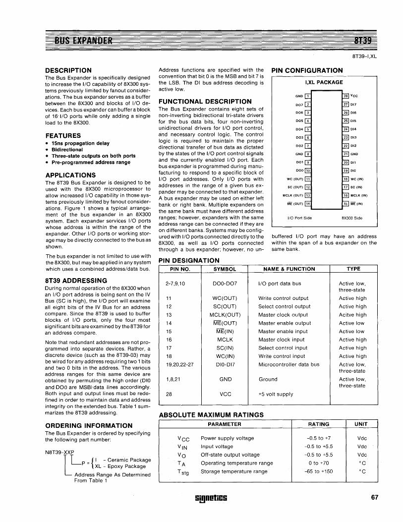
BUS EXPANDER
DESCRIPTION The Bus Expander is specifically designed to increase the I/O capability ofaX300 systems previously limited by fanout considerations. The bus expander serves as a buffer between the aX300 and blocks of I/O devices. Each bus expander can buffer a block of 161/0 ports while only adding a single load to the aX300.
FEATURES • 15ns propagation delay • Bidirectional • Three-state outputs on both ports • Pre-programmed address range
APPLICATIONS The aT39 Bus Expander is designed to be used with the aX300 microprocessor to allow increased I/O capability in those systems previously limited by fanout considerations. Figure 1 shows a typical arrangement of the bus expander in an aX300 system. Each expander services I/O ports whose address is within the range of the expander. Other I/O ports or working storage may be directly can nected to the bus as shown.
Address functions are specified with the convention that bit 0 is the MSB and bit 7 is the LSB. The 01 bus address decoding is active low.
FUNCTIONAL DESCRIPTION The Bus Expander contains eight sets of non-inverting bidirectional tri-state drivers for the bus data bits, four non-inverting unidirectional drivers for I/O port control, and necessary control logic. The control logic is required to maintain the proper directional transfer of bus data as dictated by the states of the I/O port control signals and the currently enabled I/O port. Each bus expander is programmed during manu-:facturing to respond to a specific block of I/O port addresses. Only I/O ports with addresses in the range of a given bus expander may be connected to that expander. A bus expander may be used on either left bank or right bank. Multiple expanders on the same bank must have different address ranges; however, expanders with the same address range can be connected if they are on different banks. Systems may be configured with I/O ports connected directly to the aX300, as well as I/O ports connected through a bus expander; however, no un-
8T39
aT39-I,XL
PIN CONFIGURATION
I,XL PACKAGE
1/0 Port Side 8X300 Side
buffered I/O port may have an address within the span of a bus expander on the same bank.
The bus expander is not limited to use with the aX300, but may be applied in any system PIN DESIGNATION which uses a combined address/data bus.
ST39 ADDRESSING During normal operation of the aX300 when an I/O port address is being sent on the IV Bus (SC is high), the I/O port will examine all eight bits of the IV Bus for an address compare. Since the aT39 is used to buffer blocks of I/O ports, only the four most significant bits are examined by the aT39 for an address compare.
Note that redundant addresses are not programmed into separate devices. Rather, a discrete device (such as the aT39-03) may be wired for any address requiring two 1 bits and two 0 bits in the address. The various address ranges for this same device are obtained by permuting the high order (010 and 000 are MSB) data lines accordingly. Both input and output lines must be redefined in order to maintain data and address integrity on the extended bus. Table 1 sum-
PIN NO.
2-7,9,10
11
12
13
14
15
16
17
1a
19,20,22-27
1,a,21
2a
SYMBOL NAME & FUNCTION
000-007 I/O port data bus
WC(OUT) Write control output
SC(OUT) Select control output
MCLK(OUT) Master clock output
ME(OUT) Master enable output
ME(IN) Master enable input
MCLK Master clock input
SC(IN) Select control input
WC(IN) Write control input
010-017 Microcontroller data bus
GND Ground
VCC +5 volt supply
marizes the aT39 addressing. ABSOLUTE MAXIMUM RATINGS
ORDERING INFORMATION The Bus Expander is ordered by specifying the following part number:
NaT39-XXP
LLp = {I - Ceramic Package XL - Epoxy Package
Address Range As Determined From Table 1
VCC
VIN
Vo
TA
T stg
PARAMETER RATING
Power supply voltage -0.5 to +7
Input voltage -0.5 to +5.5
Off-state output voltage -0.5 to +5.5
Operating temperature range o to +70
Storage temperature range -65 to +150
Si!)DotiCS
TYPE
Active low, three-state
Active high
Active high
Acitve high
Active low
Active low
Active high
Active high
Active high
Active low, three-state
Active low, three-state
UNIT
Vdc
Vdc
Vdc
°c °c
67
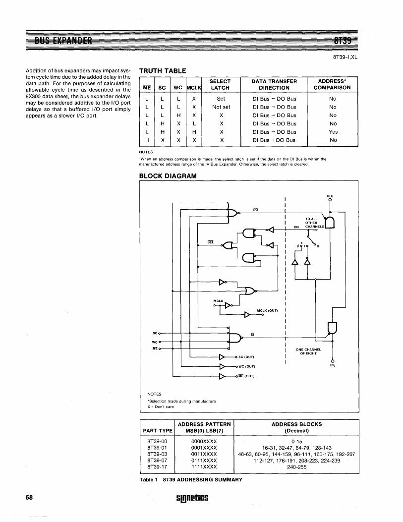
BUS [)[PANDER 8139
BT39-I,XL
Addition of bus expanders may impact sys- TRUTH TABLE tem cycle time due to the added delay in the data path. For the purposes of calculating allowable cycle time as described in the BX300 data sheet, the bus expander delays may be considered additive to the I/O port delays so that a buffered I/O port simply appears as a slower I/O port.
68
SELECT DATA TRANSFER ADDRESS* ME SC WC MCLK LATCH DIRECTION COMPARISON
L L L X Set 01 Bus .... DO Bus No
L L L X Not set 01 Bus ..... DO Bus No
L L H X X 01 Bus ..... DO Bus No
L H X L X 01 Bus ..... DO Bus No
L H X H X 01 Bus ..... DO Bus Yes
H X X X X 01 Bus - DO Bus No
NOTES
'When an address comparison is made, the select latch is set if the data on the 01 Bus is within the manufactured address range of the IV Bus Expander. Otherwise, the select latch is cleared.
BLOCK DIAGRAM
SC
wc ME
NOTES
'Selection made during manufacture X = Don't care
ADDRESS PATTERN PART TYPE MSB(O) LSB(7)
BT39-00 OOOOXXXX BT39-01 0001XXXX BT39-03 0011XXXX BT39-07 0111XXXX aT39-17 1111XXXX
DO;
El
ONE CHANNEL OF EIGHT
SC (OUT)
WC (OUT) 01;
ME (OUT)
ADDRESS BLOCKS (Decimal)
0-15 16-31,32-47,64-79,12B-143
4B-63, BO-95, 144-159,96-111,160-175,192-207 112-127,176-191, 20B-223, 224-239
240-255
Table 1 8T39 ADDRESSING SUMMARY
S!!Inotics
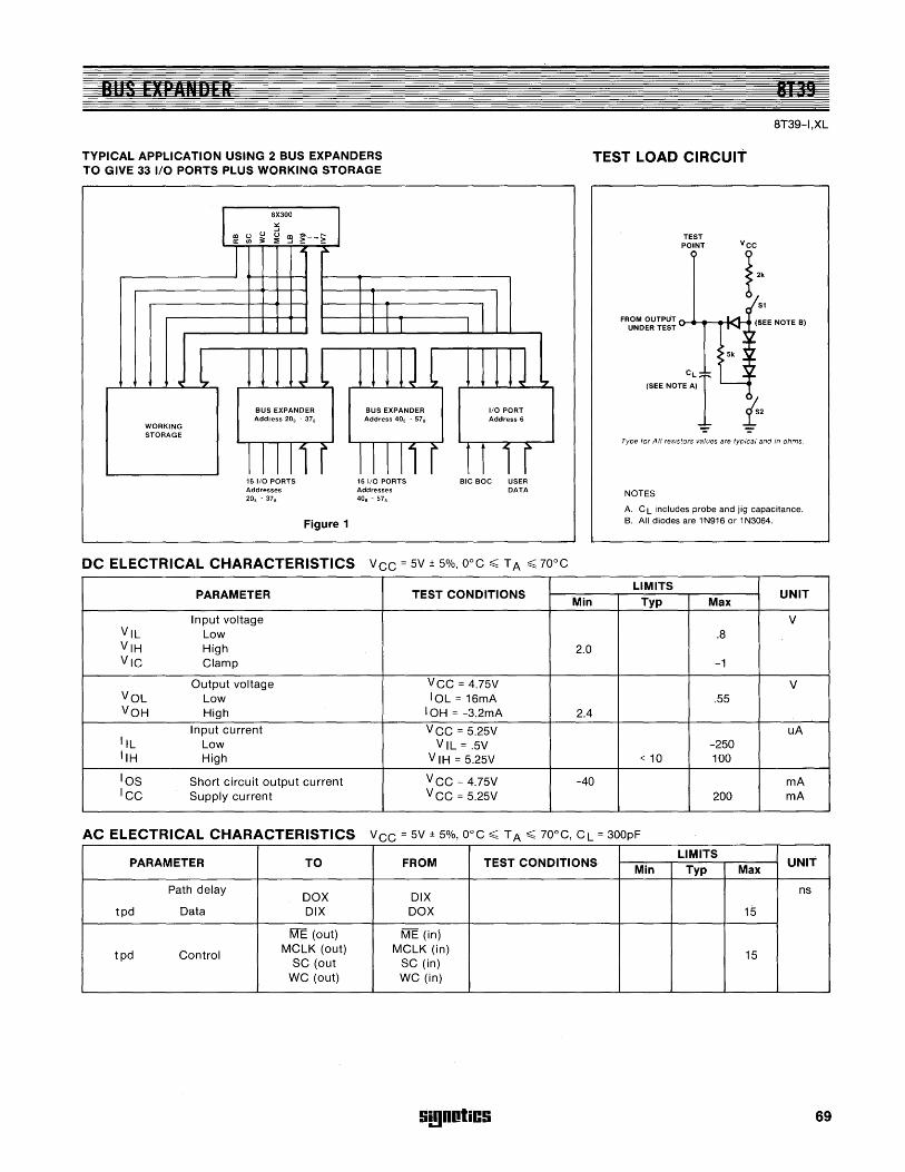
BUS EXPANDER 8T39
8T39-I,XL
TYPICAL APPLICATION USING 2 BUS EXPANDERS TO GIVE 33 1/0 PORTS PLUS WORKING STORAGE
TEST LOAD CIRCUIT
WORKING STORAGE
BUS EXPANDER Address 20, - 37,
16110 PORTS Addresses 20, . 37,
Figure 1
DC ELECTRICAL CHARACTERISTICS
PARAMETER
Input voltage VIL Low VIH High VIC Clamp
Output voltage VOL Low VOH High
Input current IlL Low IIH High
lOS Short circuit output current ICC Supply current
AC ELECTRICAL CHARACTERISTICS
PARAMETER TO
Path delay DOX
tpd Data DIX
ME (out)
tpd Control MCLK (out) SC (out
WC (out)
BUS EXPANDER Address 40, - 57,
16110 PORTS Addresses 40, - 57,
1/0 PORT Address 6
BIC BOC USER DATA
TEST CONDITIONS
VCC = 4.75V 10L = 16mA
10H = -3.2mA
VCC = 5.25V VIL = .5V
V IH = 5.25V
V CC = 4.75V V CC = 5.25V
Min
2.0
2.4
-40
Type for All resistors values are typical and in ohms.
NOTES
A. CL includes probe and jig capacitance. B. All diodes are 1N916 or 1N3064.
LIMITS UNIT
Typ Max
V .8
-1
V .55
uA -250
< 10 100
mA 200 mA
VCC = 5V ± 5%, O°C ~ T A ~ 70°C, CL = 300pF
FROM TEST CONDITIONS Min
LIMITS UNIT
Typ Max
DIX ns
DOX 15
ME (in) MCLK (in) 15
SC (in) WC (in)
Si!lDotiCS 69
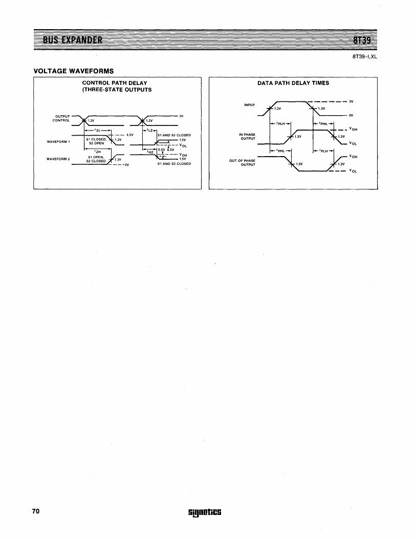
BUS (IPnNDEI
VOLTAGE WAVEFORMS
CONTROL PATH DELAY (THREE-STATE OUTPUTS
OUTPUT CONTROL
~-----3V
WAVEFORM 1
WAVEFORM 2
70
tZH
S10PEN, S2 CLOSED
--------'-- - - -OV Sl AND S2 CLOSED
Si!lDotiGS
INPUT
IN PHASE OUTPUT
OUT OF PHASE OUTPUT
BTS)
BT39-I,XL
DATA PATH DELAY TIMES
-----OV
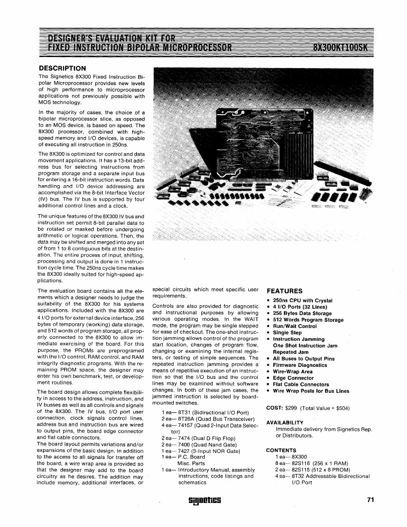
DESIGNER'S EVALUATION KIT FOR FIXED INS I RIICTION BIPOLIlR M ICIOPIOCESSOR
DESCRIPTION The Signetics 8X300 Fixed Instruction Bipolar Microprocessor provides new levels of high performance to microprocessor applications not previously possible with MOS technology.
In the majority of cases, the choice of a bipolar microprocessor slice, as opposed to an MOS device, is based on speed. The 8X300 processor, combined with highspeed memory and I/O devices, is capable of executing all instruction in 250ns.
The 8X300 is optimized for control and data movement applications. It has a 13-bit address bus for selecting instructions from program storage and a separate input bus for entering a 16-bit instruction words. Data handling and I/O device addressing are accomplished via the 8-bit Interface Vector (IV) bus. The IV bus is supported by four additional control lines and a clock.
The unique features of the 8X300 IV bus and instruction set permit 8-bit parallel data to be rotated or masked before undergoing arithmetic or logical operations. Then, the data may be shifted and merged into any set of from 1 to 8 contiguous bits at the destination. The entire process of input, shifting, processing and output is done in 1 instruction cycle time. The 250ns cycle time makes the 8X300 ideally suited for high-speed applications.
The evaluation board contains all the elements which a deSigner needs to judge the suitability of the 8X300 for his systems applications. Included with the 8X300 are
4 I/O ports for external device interface, 256 bytes of temporary (working) data storage, and 512 words of prog ram storage, all properly connected to the 8X300 to allow immediate exercising of the board. For this purpose, the PROMs are preprogramed with the I/O control, RAM control, and RAM integrity diagnostic programs. With the remaining PROM space, the designer may enter his own benchmark, test, or development routines.
The board deSign allows complete flexibility in access to the address, instruction, and IV busses as well as all controls and signals of the 8X300. The IV bus, I/O port user connection, clock signals control lines, address bus and instruction bus are wired to output pins, the board edge connector and flat cable connectors. The board layout permits variations and/or expansions of the basic design. In addition to the access to all signals for transfer off the board, a wire wrap area is provided so that the designer may add to the board circuitry as he desires. The addition may include memory, additional interfaces, or
special circuits which meet specific user requirements.
Controls are also provided for diagnostic and instructional purposes by allowing various operating modes. In the WAIT mode, the program may be single stepped for ease of checkout. The one-shot instruction jamming allows control of the program start location, changes of program flow, changing or examining the internal registers, or testing of simple sequences. The repeated instruction jamming provides a means of repetitive execution of an instruction so that the I/O bus and the control lines may be examined without software changes. In both of these jam cases, the jammed instruction is selected by boardmounted switches.
1 ea- 8T31 (Bidirectional I/O Port) 2 ea- 8T26A (Quad Bus Transceiver) 4 ea- 74157 (Quad 2-lnput Data Selec-
tor) 2 ea- 7474 (Dual DFlip Flop) 2 ea- 7400 (Quad Nand Gate) 1 ea- 7427 (3-lnput NOR Gate) 1 ea- P.C. Board
Misc. Parts 1 ea- Introductory Manual, assembly
instructions, code listings and schematics
SjgnDtics
BX300KTIOOSK
FEATURES • 250ns CPU with Crystal • 4 I/O Ports (32 Lines) • 256 Bytes Data Storage • 512 Words Program Storage • Run/Wait Control • Single Step • Instruction Jamming
One Shot Instruction Jam Repeated Jam
• All Buses to Output Pins • Firmware Diagnostics • Wire-Wrap Area • Edge Connector • Flat Cable Connectors • Wire Wrap Posts for Bus Lines
COST: $299 (Total Value = $504)
AVAILABILITY Immediate delivery from Signetics Rep. or Distributors.
CONTENTS 1 ea- 8X300 8 ea- 82S116 (256 x 1 RAM) 2 ea- 82S115 (512 x 8 PROM) 4 ea- 8T32 Addressable Bidirectional
I/O Port
71
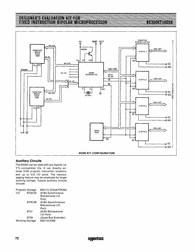
F1r C llj H' R ; I "'1' I Oi. iii I "I FllEu IllS ROC liON BIPOLAR MiERa' R"tl sgfJR
+5V RESET HALT C) C) ()
"'"- A4-A12
~ 2Nrs SIGNETICS B2S215 512xB ROM
110- 17
I-- VCC VR VCR
A4-A12 CE2 CE1
STROBE IVBO-IVB7
AO-A3 BX300 INTERPRETER MCLK,
SC,WC
'- . LB
- )I 10 115 ....... L
~ ......
SIGNETICS .... A4-A12 B2S215
512xB ROM
IB-115
CE2 CE,
---4
+5() --=
Auxiliary Circuits The 8X300 can be used with any bipolar (or TTL-compatible) ICs. It can directly address 8192 program instruction locations and up to 512 I/O ports. The memory paging feature may be employed for larger working storage. Typical auxiliary circuits include:
Program Storage 110 8T32/33
8T35/36
8T31
8T39 Working Storage
72
82S115 (512x8 PROM) (8-Bit Synchronous Bidirectional I/O Port) (8-Bit Asynchronous Bidirectional 110 Port) (8-Bit Bidirectional I/O Port) (Quad Bus Extender) 82S116 RAM
-y ~
X1G~j IND
B.O MHz
"""-
256XB RAM
~
8X300 KIT CONFIGURATION
Si!lDotiCS
-
BY u.IIK IIOUSU
SIGNETICS BT32/33 IV BYTES
... IV BYTE 1
~ -ME
I L
...
IV BYTE 2
~ ME
I I
...
IV BYTE 3
~ ME
I I
...
IV BYTE 4
L -ME
~ I
UDO-UD7 ... ">
... "" ...
UDO-UD7
>
... ... ""
UDO-UD7
">
...
...
UDO-UD7 ... ">
'" ~
BIC
BOC
BIC
BOC
BIC
BOC
BIC
BOC
SUPPORT SOFTWARE
The Microcontroller Cross Assembly Program (MCCAP) is a program designed to translate symbolic instructions into object code that can be executed by the 8X300. This program will run on most computers that have a FORTRAN compiler with a computer word length of at least 16 bits and a random access I/O capability; it can be run on most minicomputers as well as large scale computers.
The Assembler is written in FORTRAN which provides compatibility with most computer systems and makes it transportable. The program is modular and uses a minimum of memory. However, it may be operated in an overlay mode if necessary.
The Assembler is a 2-pass program that issues helpful error messages and produces an easily read program listing. During the first pass, the labels are examined and placed in a symbol table. Certain errors may be detected during this pass and will be displayed on the output listing.
In the second pass, the object code is completed, symbolic addresses are resolved, and a listing and object module are produced. Certain errors not detected during the first pass may be detected and displayed on the listing.
The Assembler features symbolic addressing, forward references and expression evaluation. It also has the capability to symbolically represent the Interface Vector (IV).
In addition, the Assembler is capable of expressing data in several number systems as well as in ASCII character codes.
MCCAP is distributed in 1 of 4 standard forms. These distribution forms are described below.
9-Track EBCDIC MagnetiC Tape This is standard IBM compatible magnetic tape recorded in 9-track format. The tape is recorded with 1 source card image per record.
Density: Record Length: Block Size:
800 BPI 80 Bytes 80 Bytes (1 record/block)
9-Track ASCII MagnetiC Tape This form is the same as 9-track EBCDIC tape except that ASCII character codes are used with the parity bit a zero.
7-Track BCD MagnetiC Tape This is standard IBM compatible magnetic tape recorded in 7-track format. The tape is recorded in even parity BCD with 1 source card image per record. Density: 800 BPI Record Length: 80 Characters Block Size: 80 Characters (1 record
/block)
029 Punch Cards Standard 80 column punched cards, punched in 029 (EBCDIC) punch codes.
Si!1DOliCS
8X300
73

74 !ii!lDotiC!i
CIIAPTIR S STAnDARD SUPPORT
CIRCUITS
!ii!l0otiC!i 75

76 !ii!lDotiC!i
INTRODUCTION In addition to the dedicated support circuits available for the various Signetics microprocessors, Signetics offers a complete line of standard circuits to complete the design of a microcomputer system.
A complete line of Schottky-clamped TTL, read/write memory arrays is offered. All feature open collector or tri-state output options for optimi~ation of word expansion in bused organizations. Memory expansion is further enhanced by full on-chip address decoding, chip enable function and PNP input transistors which reduce input loading requirements. All devices offer high performance read access and write cycle times making these devices ideally suited in high speed memory applications such as "cache," buffers, scratch pads, writable control store, main store, etc.
Signetics offers the industry's broadest line
of bipolar high performance ROMs, PROMs and FPLAs. The PROMs and FPLAs are field programmable, which means that custom patterns are immediately available by following the provided fusing procedures. Signetics PROMs are supplied with all outputs at logical O. Outputs are programmed to a logic 1 at any specified address by fusing a Ni-Cr link matrix. All bipolar ROMs, PROMs and FPLAs are fully TTL compatible, and include on-Chip decoding and chip enable functions for ease of memory expansion. Tri-state and open collector output functions are available, and low input currents reduce input buffer requirements. Most Signetics PROMs and FPLAs also have pin and performance compatible ROMs and PLAs, offering the user the ultimate in flexibility and cost reduction.
Signetics n-channel MaS products include a complete family of 1 K static RAMs and 8K
Si!lDOliCS
static ROMs. These feature TTL compatible inputs and outputs, and require only a single +5V power supply. A variety of 4K dynamic RAMs is also available for system configurations requiring large amounts of read/write memory.
The 8T series of interface devices includes display drivers, bus drivers, input/output ports, level converters, and special purpose devices. A complete line of standard and low power Schottky (LS) 74 series devices is available in addition to the 8200 series of MSI devices. Many devices from the Signetics analog product line are also suitable for use in microcomputer systems. These include voltage regulators, operational amplifiers, comparators and timers.
This chapter provides product line summaries and data for a representative selection of Signetics standard support circuits. Further information can be found in the Signetics Data Manual.
77
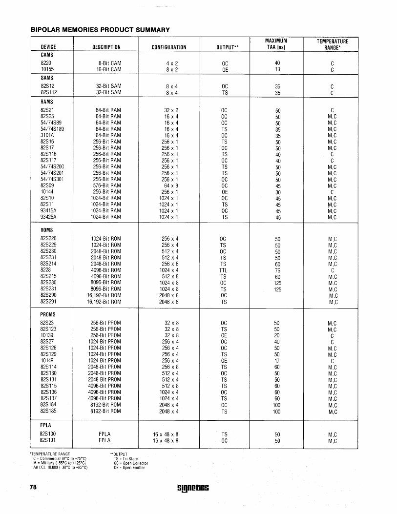
BIPOLAR MEMORIES PRODUCT SUMMARY
DEVICE CAMS
8220 10155
SAMS
82S12 82S 112
RAMS
82S21 82S25 54174S89 54174S 189 3101A 82S16 82S17 82S116 82S 117 54/74S200 54/74S201 54/74S301 82S09 10144 82S10 82S11 93415A 93425A
ROMS
82S226 82S229 82S230 82S231 82S214 8228 82S215 82S280 82S281 82S290 82S291
PROMS
82S23 82S123 10139 82S27 82S126 82S129 10149 82S114 82S130 82S131 82S115 82S136 82S137 82S184 82S185
FPLA
82S100 82S101
'TEMPERATURE RANGE C = Commercial (O°C to +75°C) M = Military (-55°C to +125°C) All ECl 10,000 (-30°C to +85°C)
78
DESCRIPTION
8-Bit CAM 16-Bit CAM
32-Bit SAM 32-Bit SAM
64-Bit RAM 64-Bit RAM 64-Bit RAM 64-Bit RAM 64-Bit RAM
256-Bit RAM 256-Bit RAM 256-Bit RAM 256-Bit RAM 256-Bit RAM 256-Bit RAM 256-Bit RAM 576-Bit RAM 256-Bit RAM
1024-Bit RAM 1024-Bit RAM 1024-Bit RAM 1024-Bit RAM
1024-Bit ROM 1024-Bit ROM 2048-Bit ROM 2048-Bit ROM 2048-Bit ROM 4096-Bit ROM 4096-Bit ROM 8096-Bit ROM 8096-B it ROM
16,192-Bit ROM 16,192-Bit ROM
256-Bit PROM 256-Bit PROM 256-Bit PROM
1024-Bit PROM 1024-Bit PROM 1024-Bit PROM 1024-Bit PROM 2048-Bit PROM 2048-Bit PROM 2048-Bit PROM 4096-Bit PROM 4096-Bit PROM 4096-Bit PROM 8192-Bit ROM 8192-Bit ROM
FPLA FPLA
"OUTPUT TS = Tri-State OC = Open Collector OE = Open Emitter
CONFIGURATION
4 x 2 8 x 2
8 x 4 8x4
32 x 2 16 x 4 16 x 4 16 x 4 16 x 4
256 x 1 256 x 1 256 x 1 256 x 1 256 x 1 256 x 1 256 x 1
64 x 9 256 x 1
1024 x 1 1024 x 1 1024 x 1 1024 x 1
256 x 4 256 x 4 512 x 4 512 x 4 256 x 8
1024 x 4 512 x 8
1024 x 8 1024 x 8 2048 x 8 2048 x 8
32 x 8 32 x 8 32 x 8
256 x 4 256 x 4 256 x 4 256 x 4 256 x 8 512 x 4 512 x 4 512 x 8
1024 x 4 1024 x 4 2048 x 4 2048 x 4
16 x 48 x 8 16 x 48 x 8
Si!lDOliCS
MAXIMUM TEMPERATURE OUTPUT** TAA Ins) RANGE*
OC 40 C OE 13 C
OC 35 C TS 35 C
OC 50 C OC 50 M,C OC 50 M,C TS 35 M,C OC 35 M,C TS 50 M,C OC 50 M,C TS 40 C OC 40 C TS 50 M,C TS 50 M,C OC 50 M,C OC 45 M,C OE 30 C OC 45 M,C TS 45 M,C OC 45 M,C TS 45 M,C
OC 50 M,C TS 50 M,C OC 50 M,C TS 50 M,C TS 60 M,C
TTL 75 C TS 60 M,C OC 125 M,C TS 125 M,C OC M,C TS M,C
OC 50 M,C TS 50 M,C OE 20 C OC 40 C OC 50 M,C TS 50 M,C OE 17 C TS 60 M,C OC 50 M,C TS 50 M,C TS 60 M,C OC 60 M,C TS 60 M,C OC 100 M,C TS 100 M,C
TS 50 M,C OC 50 M,C
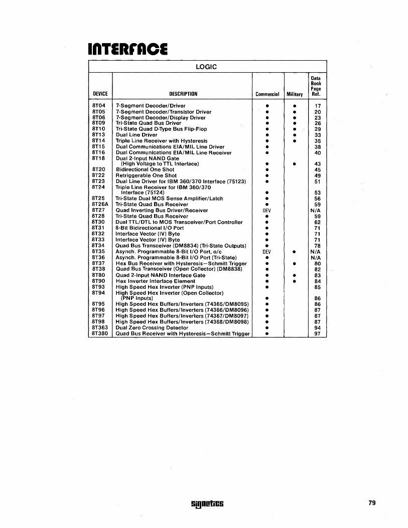
InTIRrACI LOGIC
Data Book Page
DEVICE DESCRIPTION Commercial Military Ref.
ST04 7-Segment Decoder/Driver • • 17 ST05 7-Segment Decoder/Transistor Driver • • 20 ST06 7-Segment Decoder/Display Driver • • 23 ST09 Tri-State Quad Bus Driver • • 26 ST10 Tri-State Quad D-Type Bus Flip-Flop • • 29 ST13 Dual Line Driver • • 33 ST14 Triple Line Receiver with Hysteresis • • 35 ST15 Dual Communications EIA/MIL Line Driver • 3S ST16 Dual Communications EIA/MIL Line Receiver • 40 ST1S Dual 2-lnput NAND Gate
(High Voltage to TTL Interface) • • 43 ST20 Bidirectional One Shot • 45 ST22 Retriggerable One Shot • 49 ST23 Dual Line Driver for IBM 360/370 Interface (75123) • 51 ST24 Triple Line Receiver for IBM 360/370
Interface (75124) • 53 ST25 Tri-State Dual MOS Sense Amplifier/Latch • 56 ST26A Tri-State Quad Bus Receiver • 59 ST27 Quad Inverting Bus Driver/Receiver DEV N/A ST2S Tri-State Quad Bus Receiver • 59 ST30 Dual TTL/DTL to MOS Transceiver/Port Controller • 62 ST31 S-Bit Bidirectional I/O Port • 71 ST32 Interface Vector (IV) Byte • 71 ST33 Interface Vector (IV) Byte • 71 ST34 Quad Bus Transceiver (DMSS34) (Tri-State Outputs) • 7S ST35 Asynch. Programmable S-Bit I/O Port, o/c DEV • N/A ST36 Asynch. Programmable S-Bit I/O Port (Tri-State) • N/A ST37 Hex Bus Receiver with Hysteresis-Schmitt Trigger • • SO ST3S Quad Bus Transceiver (Open Collector) (DMSS3S) • S2 STSO Quad 2-lnput NAN D Interface Gate • • S3 ST90 Hex Inverter Interface Element • • S4 ST93 High Speed Hex Inverter (PNP Inputs) • S5 ST94 High Speed Hex Inverter (Open Collector)
(PNP Inputs) • S6 ST95 High Speed Hex Buffers/Inverters (74365/DMS095) • S6 ST96 High Speed Hex Buffers/Inverters (74366/DMS096) • S7 ST97 High Speed Hex Buffers/Inverters (74367/DMS097) • S7 ST9S High Speed Hex Buffers/Inverters (7436S/DMS09S) • S7 ST363 Dual Zero Crossing Detector • 94 ST3S0 Quad Bus Receiver with Hysteresis-Schmitt Trigger • 97
!i!!)DotiC!i 79
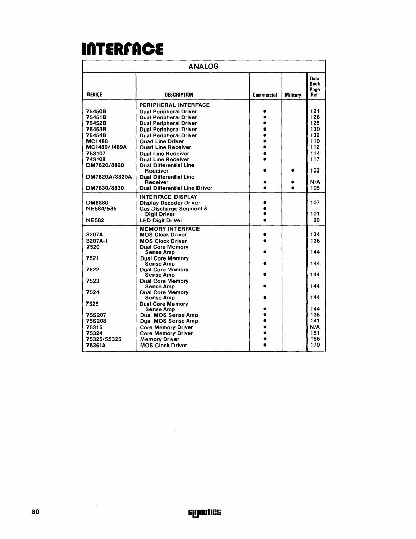
InTERfnOE ANALOG
Data Book Page
DEVICE DESCRIPTION Commercial Military Ref.
PERIPHERAL INTERFACE 754508 Dual Peripheral Driver • 121 754518 Dual Peripheral Driver • 126 754528 Dual Peripheral Driver • 128 754538 Dual Peripheral Driver • 130 754548 Dual Peripheral Driver • 132 MC1488 Quad Line Driver • 110 MC1489/1489A Quad Line Receiver • 112 75S107 Dual Line Receiver • 114 74S108 Dual Line Receiver • 117 DM7820/8820 Dual Differential Line
Receiver • • 103 DM7820A/8820A Dual Differential Line
Receiver • • N/A DM7830/8830 Dual Differential Line Driver • • 105
INTERFACE DISPLAY DM8880 Display Decoder Driver • 107 NE584/585 Gas Discharge Segment & •
Digit Driver • 101 NE582 LED Digit Driver • 99
MEMORY INTERFACE 3207A MOS Clock Driver • 134 3207A-1 MOS Clock Driver • 136 7520 Dual Core Memory
Sense Amp • 144 7521 Dual Core Memory
Sense Amp • 144 7522 Dual Core Memory
Sense Amp • 144 7523 Dual Core Memory
Sense Amp • 144 7524 Dual Core Memory
Sense Amp • 144 7525 Dual Core Memory
Sense Amp • 144 75S207 Dual MOS Sense Amp • 138 75S208 Dual MOS Sense Amp • 141 75315 Core Memory Driver • N/A 75324 Core Memory Driver • 151 75325/55325 M emory Driver • 156 75361A MOS Clock Driver • 170
80 Gi!l00liCG
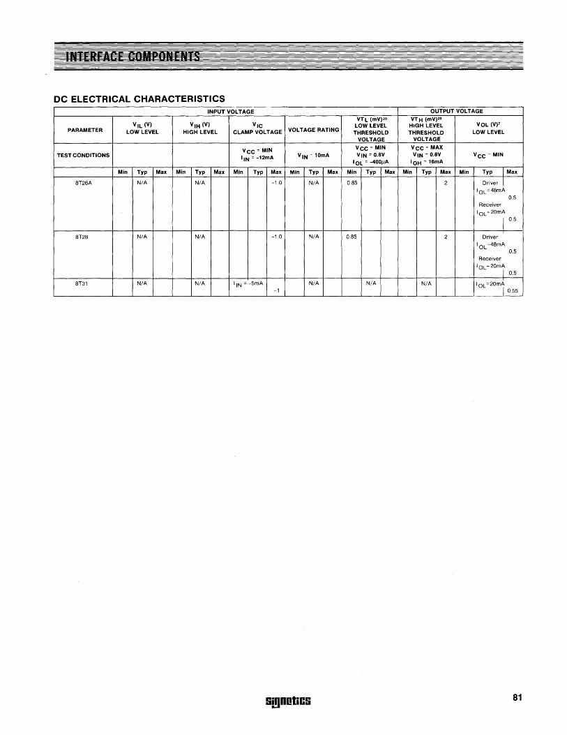
IN I EltrAcE COMPONENTS
DC ELECTRICAL CHARACTERISTICS INPUT VOLTAGE OUTPUT VOLTAGE
VTL (mV)20 VTH (mV)2o VIL (V) V IH (V) VIC LOW LEVEL HIGH LEVEL VOL (V)1
PARAMETER LOW LEVEL HIGH LEVEL CLAMP VOLTAGE VOLTAGE RATING THRESHOLD THRESHOLD LOW LEVEL VOLTAGE VOLTAGE
VCC = MIN VCC = MIN VCC = MAX TEST CONDITIONS liN = -12mA V IN = 10mA VIN = O.8V VIN = O.8V VCC = MIN
IOL = -400f.1A IOH ~ 16mA
Min Typ Max Min Typ Max Min Typ Max Min Typ Max Min Typ Max Min Typ Max Min Typ I Max
8T26A N/A N/A -1.0 N/A 0.85 2 Driver I IOL =48mA
0.5 Receiver
IOL =20mA
I 0.5
8T28 N/A N/A -1.0 N/A 0.85 2 Driver
IOL =48mA 0.5
Receiver IOL=20mA
I 0.5
8T31 N/A N/A liN = -5mA N/A N/A N/A IOL=20mA -1 I 0.55
Si!l0otiCS 81
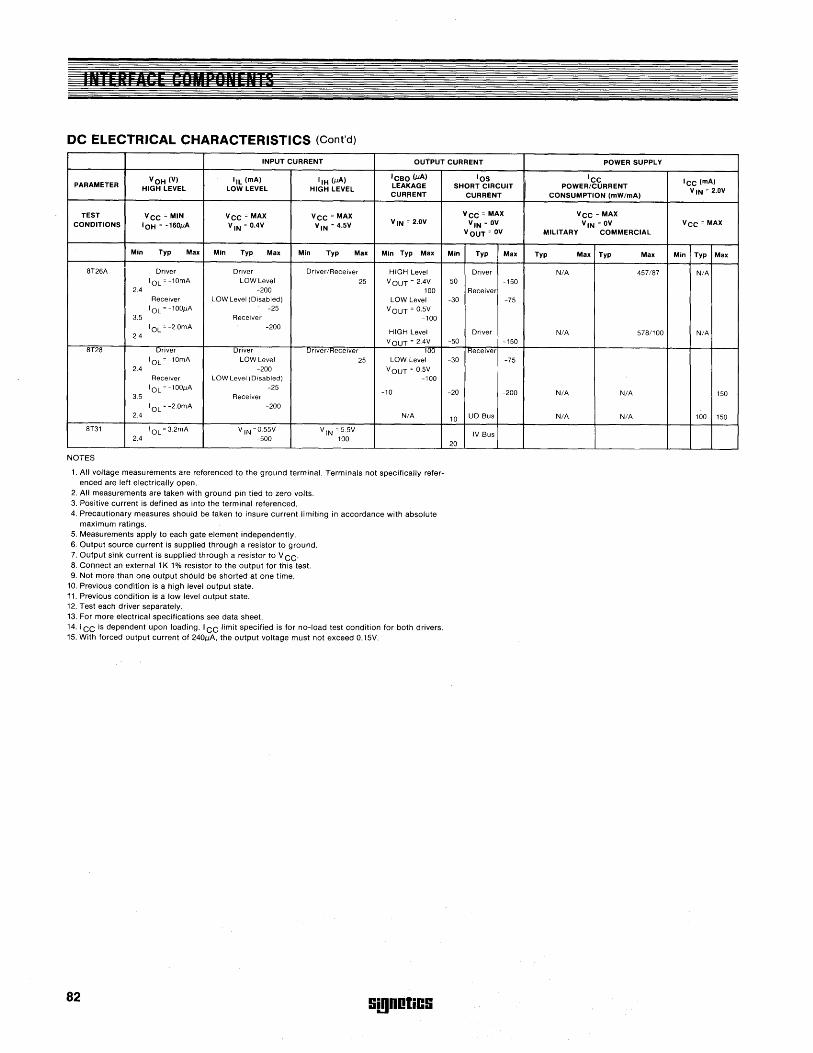
IN I ERFACE COMPO'!EN IS
DC ELECTRICAL CHARACTERISTICS (Cont'd)
INPUT CURRENT OUTPUT CURRENT POWER SUPPLY
VOH (V) IlL (rnA) IIH (iJA) ICBO (iJA) lOS ICC ICC (rnA) PARAMETER HIGH LEVEL LOW LEVEL HIGH LEVEL LEAKAGE SHORT CIRCUIT POWER/CURRENT VIN" 2.0V CURflENT CURRENT CONSUMPTION (mW/mA)
TEST VCC " MIN VCC "MAX VCC "MAX VCC = MAX VCC "MAX
CONDITIONS 10H = -160iJA V IN "O.4V V IN "4.5V VIN " 2.0V VIN "OV VIN "OV VCC" MAX
VOUT" OV MILITARY COMMERCIAL
Min Typ Max Min Typ Max Min Typ Max Min Typ Max Min Typ Max Typ Max Typ Max Min Typ Max
8T26A Driver Driver Driver/Receiver HIGH Level Driver N/A 457/87 N/A IOL =-10mA LOW Level 25 VOUT" 2.4V 50 -150
2.4 -200 100 Receiver Receiver LOW Level (Disabled) LOW Level -30 -75
IOL "-100IlA -25 V OUT " 0.5V 3.5 Receiver -100
IOL "-2.0mA -200 HIGH Level Driver N/A 578/100 N/A 2.4
VOUT" 2.4V -50 -150 8T28 Driver Driver Uriver/Hecelver 1uu I Hecelver
I OL "-10mA LOW Level 25 LOW Level -30 -75 2.4 -200 V OUT " 0.5V
Receiver LOW Level (Disabled) -100
IOL "-100IlA -25 -10 -20 -200 N/A N/A 3.5 Receiver 150
IOL "-2.0mA -200 2.4 N/A 10 UD Bus N/A N/A 100 150
8T31 IOL "3.2mA V IN =0.55V V IN " 5.5V IV Bus
2.4 -500 100 20
NOTES
1. All voltage measurements are referenced to the ground terminal. Terminals not specifically refer-enced are left electrically open.
2. All measurements are taken with ground pin tied to zero volts. 3. Positive current is defined as into the terminal referenced. 4. Precautionary measures should be taken to insure current limiting in accordance with absolute
maximum ratings. 5. Measurements apply to each gate element independently. 6. Output source current is supplied through a resistor to ground. 7. Output sink current is supplied through a resistor to V cc. 8. Connect an external 1 K 1 % resistor to the output for this test. 9. Not more than one output shOuld be shorted at one time.
10. Previous condition is a high level output state. 11. Previous condition is a low level output state. 12. Test each driver separately. 13. For more electrical specifications see data sheet. 14. I CC is dependent upon loading. I CC limit specified is for no-load test condition for both drivers. 15. With forced output current of 240I1A, the output voltage must not exceed 0.15V.
82 S!!IDotiCS
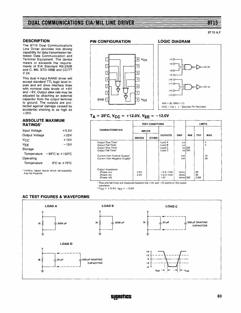
DIIAL COMMUNICATIONS EIA MIL LINE DRIVER 8T15
BT15 A,F
DESCRIPTION The BT15 Dual Communications Line Driver provides line driving capability for data transmission between Data Communication and Terminal Equipment. The device meets or exceeds the requirements of EIA Standard RS-232B and C, MIL STD-1BBB and CCITT V 24.
This dual 4-input NAND driver will accept standard TTL logic level inputs and will drive interface lines with nominal data levels of + 6V and - 6V. Output slew rate may be adjusted by attaching an external capacitor from the output terminal to ground. The outputs are protected against damage caused by accidental shorting to as high as ±25V.
ABSOLUTE MAXIMUM RATINGS*
Input Voltage +5.5V
Output Voltage ±25V
VCC +15V
VEE -15V
Storage
Temperature -65°C to + 150°C
Operating
Temperature O°C to +75°C
* Limiting values above which serviceability may be impaired.
AC TEST FIGURES & WAVEFORMS
LOAD A
LOADD
PIN CONFIGURATION LOGIC DIAGRAM
(1)~ (2)
(5)
(3)
(4) (10)2Jo (11) ,.... "-... r.
~(9)
(12)
(13)
VEE = (8) GND = (7)
VCC = (14) ( ) = Denotes Pin Numbers
TA = 25°C, VCC = +12.0V, VEE = -12.0V
TEST CONDITIONS LIMITS
CHARACTERISTICS INPUTS
OUTPUTS UNIT MIN TYP MAX DRIVEN OTHER
Output Rise Time1 Load A }LS 4 Output Fall Time1 Load B }LS 4 Output Rise Time1 Load C ns 200 Output Fall Time1 Load D ns 200
Current from Positive Supply2 mA 16 Current from Negative Supply2 mA 28
Output Impedance (Power on) O.OV -3.5±1mA ohms 95 (Power on) 2.0V +3.5±1mA ohms 95 (Power off) ±2V ohms 300 2.5M
1 Rise and fall times are measured between the +3V and -3V points on the output waveform.
2 VCC = +12.6V, VEE = -12.6V
LOADB LOADC
7k h ::-----lsooPFSHAPING
~ _------J CAPACITOR
3k h :p~-----lsOOPFSHAPING ~ _------J CAPACITOR
+61 I +3 - - - - - - - - - - - -
o ~ J
-3 f- --- -\---1 ~----6 tfall __ ~ =I f-- trise
Iil!lnDliCIi 83
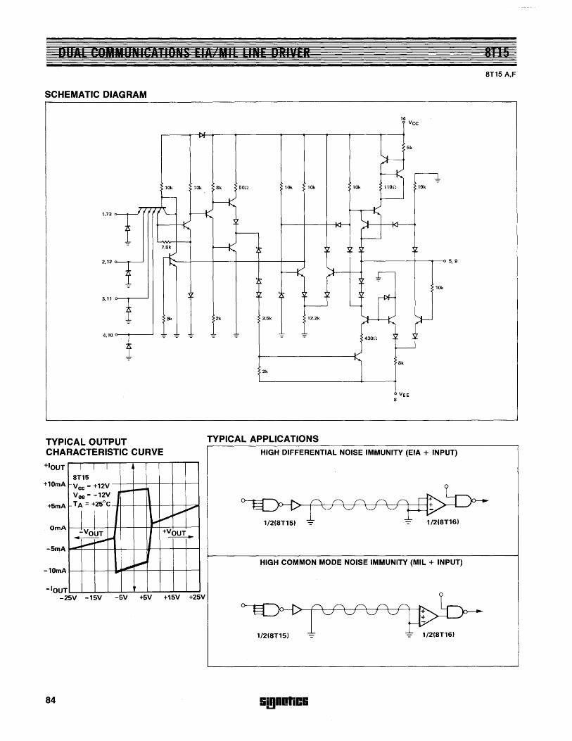
'''IAI I ''''''"NIOATIO,,5 fill Mi' LINE np"'ER
SCHEMATIC DIAGRAM
14 Vee
5k
10k 10k 8k son iOk iOk iOk 19k
1.73
3,11 0--...-----'
4,10 0---......----'
TYPICAL OUTPUT CHARACTERISTIC CURVE
+IOUT I I I 8T15 Vee = +12V -+10mA
Vee = -12V -+5mA TA = +25°C
5k
I \ to-' ~ ~ ~
-VOUT +VOUT .. ---~~
OmA
-5mA .--""""" .JIll ~ -10mA
-lOUT -25V -15V -5V +5V +15V +25V
84
+------+-__.-----<l 5,9
10k
2k 3.5k 12.2k
2k
TYPICAL APPLICATIONS HIGH DIFFERENTIAL NOISE IMMUNITY (EIA + INPUT)
HIGH COMMON MODE NOISE IMMUNITY (MIL + INPUT)
SmAOlies
8115 8T1S A,F
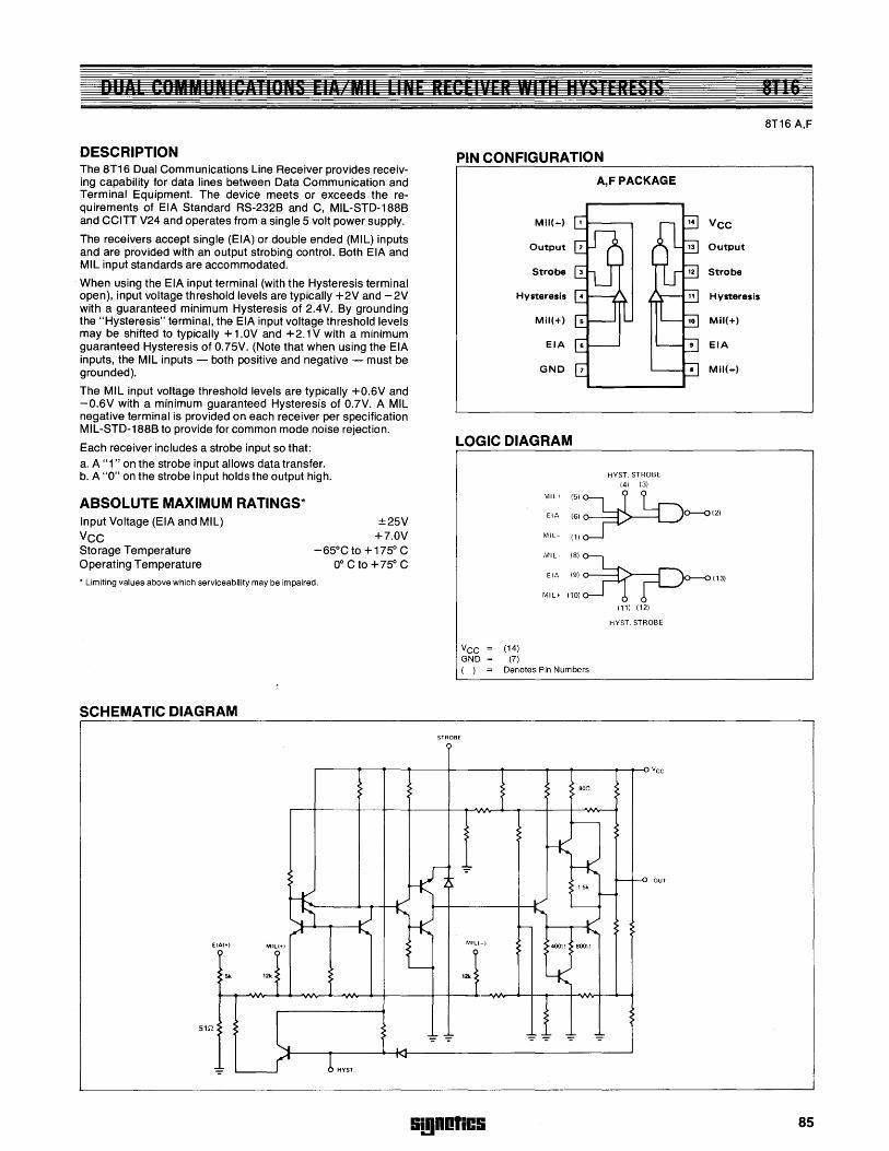
DUhE COM. UN ICI\110HS Elft M I E LI HE IEIt IIEI vv III illS I EitESIS
DESCRIPTION The 8T16 Dual Communications Line Receiver provides receiving capability for data lines between Data Communication and Terminal Equipment. The device meets or exceeds the requirements of EIA Standard RS-232B and C, MIL-STD-188B and CCITT V24 and operates from a single 5 volt power supply.
The receivers accept single (EIA) or double ended (MIL) inputs and are provided with an output strobing control. Both EIA and MIL input standards are accommodated.
When using the EIA input terminal (with the Hysteresis terminal open), input voltage threshold levels are typically +2V and -2V with a guaranteed minimum Hysteresis of 2.4V. By grounding the "Hysteresis" terminal, the EIA input voltage threshold levels may be shifted to typically + 1.0V and +2.1 V with a minimum guaranteed Hysteresis of 0.75V. (Note that when using the EIA inputs, the MIL inputs - both positive and negative - must be grounded).
The MIL input voltage threshold levels are typically +0.6V and -0.6V with a minimum guaranteed Hysteresis of 0.7V. A MIL negative terminal is provided on each receiver per specification MIL-STD-188B to provide for common mode noise rejection.
Each receiver includes a strobe input so that: a. A "1" on the strobe input allows data transfer. b. A "0" on the strobe input holds the output high.
ABSOLUTE MAXIMUM RATINGS* Input Voltage (EIA and MIL)
VCC
PIN CONFIGURATION
A,FPACKAGE
MiI(-)
Output 2
Strobe 3
Hysteresis 4
MiI(+)
EIA
GND
LOGIC DIAGRAM
EIA
Mil(-)
Storage Temperature Operating Temperature
±25V +7.0V
-65°C to + 175° C 0° C to +75° C
* Limiting values above which serviceability may be impaired.
:II~- :::~O-O(13) MILt(10)~ ~
SCHEMATIC DIAGRAM
EIAI>} MILl>}
51< 12k
51r2
STROBE
vee = (14) GND = (7) ( ) = Denotes Pin Numbers
(11) (12)
HYST. STROBE
.-----+_-4~_+----~------~----~--+_----~~_Ovcc
80~
OUT
MILl-I
12k
HYST
SmOOliCS
81110
8T16 A,F
85
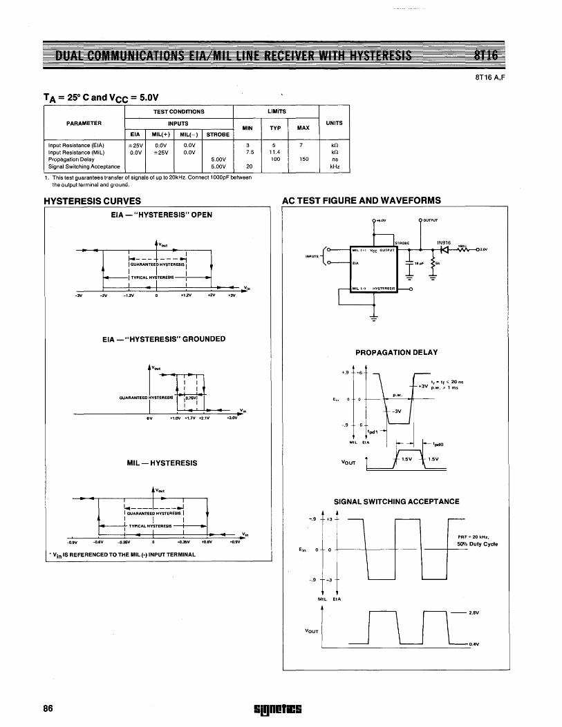
L "lOAMI" NICAfiLNb Ell Mil [INERE' EliER ."IH ii' it "EalS ITI'
TA = 250 C and VCC = 5.0V TEST CONDITIONS
PARAMETER INPUTS MIN
EIA MIL{+) MIL{-) STROBE
Input Resistance (EIA) ±25V O.OV O.OV 3 Input Resistance (MIL) O.OV ±25V O.OV 7.5 Propagation Delay 5.00V Signal Switching Acceptance 5.00V 20
1. This test guarantees transfer of signals of up to 20kHz. Connect 1 OOOpF between the output terrninal and ground.
HYSTERESIS CURVES
EIA - "HYSTERESIS" OPEN
l...---.d---~ I GUARANTEED HYSTERESIS I
....-: TYPICAL HY~TERESIS -...;:--~ -'SV -2v -1.2V +'.2V +2V +'SV
EIA -"HYSTERESIS" GROUNDED
r· ·~X iJ GUARANTEED HYSTERESIS I jo.75VI I
I ! I.: !. ,. OV +,.ov +'.7V +2.1V +3.0V
MIL - HYSTERESIS
tvout
L...----L---.J I GUARANTEED HYSTERESIS I I I I
.... __ -!-i
l TYPICAL HYSTERESIS -+-1 -_ .... 1
I I
-O.9V -O.6V -O.35V +O.35V +O.6V +O.9V
• Vin IS REFERENCED TO THE MIL (-) INPUT TERMINAL
86
8T16 A,F
LIMITS
UNITS TYP MAX
5 7 kD. 11.4 kD. 100 150 ns
kHz
AC TEST FIGURE AND WAVEFORMS
1I1!110liCIi
+.9 +3
+5.0V
PROPAGATION DELAY
+.9 +6
-.9
MIL EIA
VOUT
I, - If .; 20 ns +3V p.w. " 1 ms
SIGNAL SWITCHING ACCEPTANCE
PRF = 20 kHz,
50"10 Duty Cycle ----l---
-.9 -3
MIL EIA
VOUTI~_~_ _ 0.4V
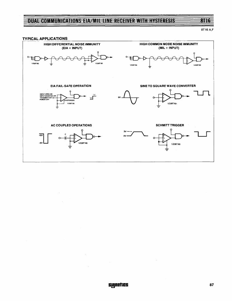
""At COMMIINICA'IONS EIA Mil liNE RECEIVER I'IIR HYSIERE-;IS
TYPICAL APPLICATIONS HIGH DIFFERENTIAL NOISE IMMUNITY
(EIA + INPUT)
EIA FAIL-SAFE OPERATION
"'" INPUT OPEN OR INPUT SHORTEO OR TRANSMITTER POWER OFF
.~
AC COUPLED OPERATIONS
~I -6VU
HIGH COMMON MODE NOISE IMMUNITY (MIL + INPUT)
SINE TO SQUARE WAVE CONVERTER
1/2(8T161
SCHMITT TRIGGER
3V-r---\.
OV~ ~
Il!IIOliC9
8T16
8T16 A,F
87
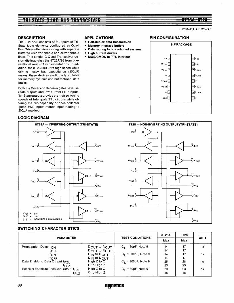
101 S I ATF QUAD BUS I RANSGEIVER
DESCRIPTION The 8T26A/28 consists of four pairs of TriState logic elements configured as Quad Bus Drivers/Receivers along with separate buffered receiver enable and driver enable lines. This single IC Quad Transceiver design distinguishes the 8T26A/28 from conventional multi-IC implementations. In addition, the 8T26/28's ultra high speed while driving heavy bus capacitance (300pF) makes these devices particularly suitable for memory systems and bidirectional data buses.
Both the Driver and Receiver gates have TriState outputs and low-current PNP inputs. Tri-State outputs provide the high switching speeds of totem pole TTL circuits while offering the bus capability of open collector gates. PNP inputs reduce input loading to 200fJ.A maximum.
LOGIC DIAGRAM
APPLICATIONS • Half-duplex data transmission • Memory interface buffers • Data routing in bus oriented systems • High current drivers • MOS/CMOS-to-TTL interface
8T261' 8T28
8T26A-B,F • BT28-B,F
PIN CONFIGURATION
B,FPACKAGE
8T26A -INVERTING OUTPUT (TRI-STATE) 8T28 - NON-INVERTING OUTPUT (TRI-STATE)
8T26A 8T28 PARAMETER TEST CONDITIONS UNIT
Max Max
Propagation Delay tON DOUT to ROUT C L = 30pF, Note 9 14 17 ns
tOFF DOUT to ROUT 14 17
tON D IN to DOUT C L = 300pF, Note 9 14 17 ns tOFF DIN to DOUT 14 17
Data Enable to Data Output t PZL High Z to 0 C L = 300pF, Note 9 25 28 ns tpLZ o to High Z 20 23
Receiver Enable to Receiver Output t PZL High Z to 0 C L = 30pF, Note 9 20 23 ns tpLZ o to High Z 15 18
88 Gi!lDOliCG
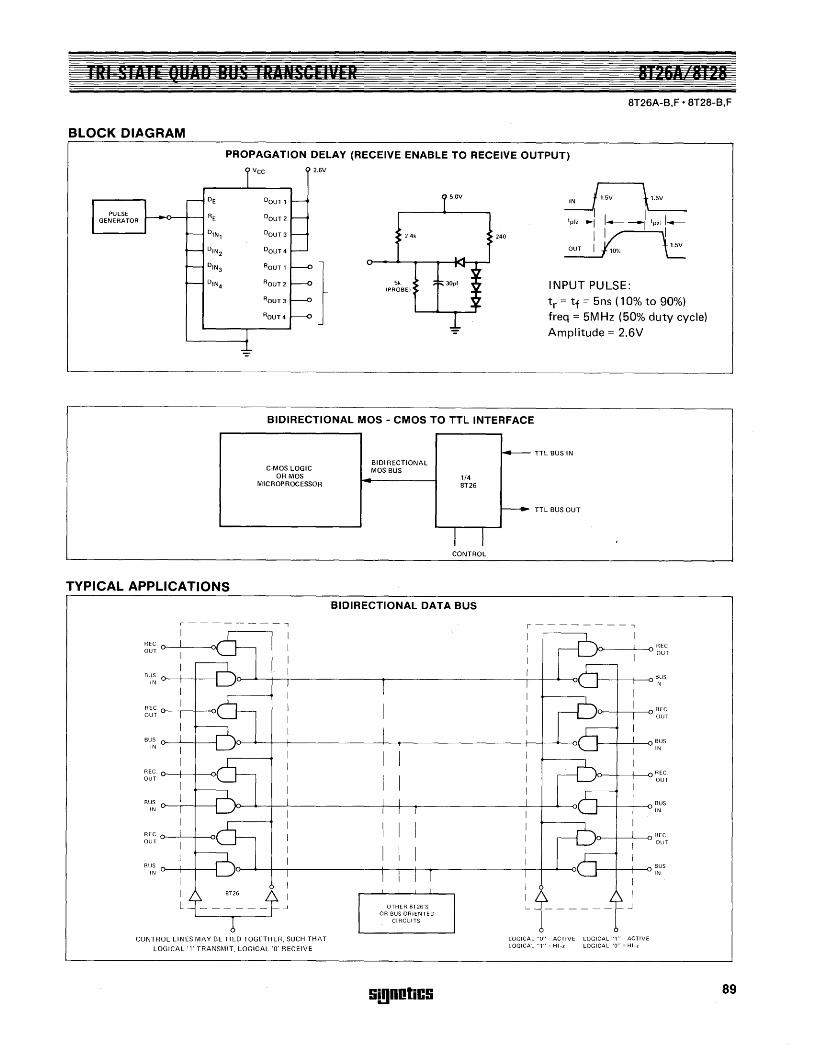
Til STATE QUAD 8US TRANSCEIVER 8T2611 8T28 BT26A-B,F· BT2B-B,F
BLOCK DIAGRAM
PROPAGATION DELAY (RECEIVE ENABLE TO RECEIVE OUTPUT)
Vcc 2.GV
DE DOUT , S.OV
RE DOUT 2 1 1 tplz __ I 1--- _I tpzl 1---
DIN, DOUT 3 2.4k 240
~ DIN2 DOUT4
DIN3 ROUT'
} DIN4 ROUT 2 Sk INPUT PULSE: (PROBEI
ROUT3 tr = tf = 5ns (10% to 90%) ROUT4 freq = 5MHz (50% duty cycle)
-= Amplitude = 2.6V
-=
BIDIRECTIONAL MOS - CMOS TO TTL INTERFACE
C·MOS LOGIC OR MOS
MICROPROCESSOR
TYPICAL APPLICATIONS
r----------,
B~~ o---+--+-~
REC o--~-I----<Cl( OUT
R EC O--l--I----<Cl( OUT
B~~ O-~--l---I
R EC 0--..1---+-01 OUT
B~~ O---+--+-~
CONTROL LINES MAY BE TIED TOGETHER, SUCH THAT
LOGICAL '1' TRANSMIT, LOGICAL '0' RECEIVE
BIDIRECTIONAL MOS BUS
1/4 8T26
I I CONTROL
BIDIRECTIONAL DATA BUS
OTHER 8T26'S OR BUS ORIENTED
CIRCUITS
Si!lDDtiCS
f.4-- TTL BUS IN
~ TTL BUS OUT
,--------.,
~--+-f---o BUS IN
~--+---.JL-.-o BUS IN
)o---l--,---o REC OUT
IO---+-L--o REC OUT
~--+-f---o ~~S
~1---- -LOGICAL "0" = ACTIVE LOGICAL "1' - ACTIVE LOGICAL "1" = HI-z LOGICAL "0" HI-z
89
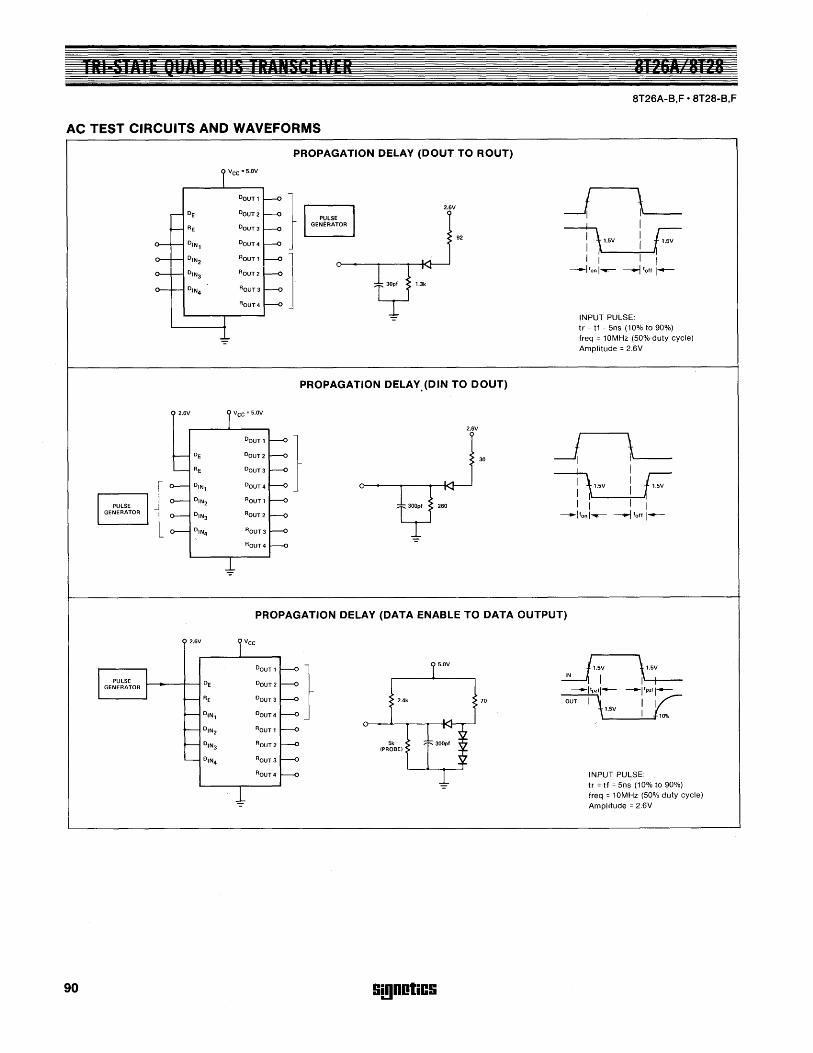
I S I liTE QUAD BUS IIIlNSCEIYEI
AC TEST CIRCUITS AND WAVEFORMS
PROPAGATION DELAY (DOUT TO ROUT)
Vee = S.ov
DOUT'
2.6V DE DOUT2
RE DOUT3
92 DIN, DOUT4
DIN2 ROUT'
DIN3 ROUT2
DIN4 ROUT 3
ROUT4
PROPAGATION DELAYJDIN TO DOUT)
2.6V Vee = S.OV
2.6V
DOUT ,
DE DOUT2 30
RE DOUT3
{ DIN, DOUT4
DIN2 ROUT'
DIN3 ROUT 2
DIN4 ROUT3
ROUT4
81261 8128 8T26A-B,F· 8T28-B,F
INPUT PULSE: tr = tf = 5ns (10% to 90%) freq = 10MHz (50% duty cycle) Amplitude = 2.6V
PROPAGATION DELAY (DATA ENABLE TO DATA OUTPUT)
2.6V Vee
DOUT ,
} DE DOUT2
RE DOUT3
DIN, DOUT4
DIN2 ROUT'
DIN3 ROUT 2
DIN4 ROUT3
ROUT4
90
S.OV
2.4k 70
Sk (PROBE)
ii!!lDotiCS
r:::--1,.SV
~I h---i'pzll- -I'pzll-~. ii/
~,o%
INPUT PULSE: tr = tf = 5ns (10% to 90%) freq = 10MHz (50% duty cycle) Amplitude = 2.6V
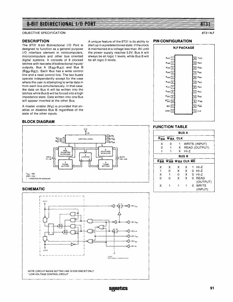
n III I BI UI IEfn IUNAE I Ii Pili I
OBJEctiVE SPECIFICATION
DESCRIPTION The 8T31 8-bit Bidirectional I/O Port is deSigned to function as a general purpose I/O interface element in minicomputers, microcomputers and other bus oriented digital systems. It consists of 8 clocked latches with two sets of bidirectional inputs/ outputs, Bus A (B AO-B A7) and Bus B (BBO-BB7). Each Bus has a write control line and a read control line. The two buses operate independently except for the case where the user is attempting to write data in from each bus simultaneously. In that case, the data on Bus A will be written into the latches while Bus B will be forced into a high impedance state. Data written into one Bus will appear inverted at the other Bus.
A master enable (M E) is provided that enables or disables Bus B regardless of the state of the other inputs.
BLOCK DIAGRAM
Vee = (24)
GND = (12)
BUSA (1)-(8)
eLK
( ) DENOTES PIN NUMBERS
SCHEMATIC
1-------------1 I BUS A I I I I I I I I I I I I I I
I I I I I BUS B I L _____________ ~
A unique feature of the 8T31 is its ability to start up in a predetermined state. If the clock is maintained at a voltage less than .8V until the power supply reaches 3.5V, Bus A will always be all logic 1 levels, while Bus B will be all logic 0 levels.
*LVCC
BUS B (16)-(23)
(INTERNALLY GENERATED)
NOTE: CIRCUIT INSIDE DOTTED LINE IS FOR ONE BIT ONLY. * LOW VOLTAGE CONTROL CIRCUIT
Si!)OOtiCS
8131
8T31 N,F
PIN CONFIGURATION
N,FPACKAGE
FUNCTION TABLE
BUSA
RBA WBA CLK
X 0 1 WRITE (INPUT) 0 1 X READ (OUTPUT) 1 1 X HI-Z
BUS B
RBB WBB WBA CLK ME
X X X X 1 HI-Z 1 0 X X 0 HI-Z X 1 0 X 0 HI-Z 0 0 X X 0 READ
(OUTPUT) X 1 1 1 0 WRITE
(INPUT)
91
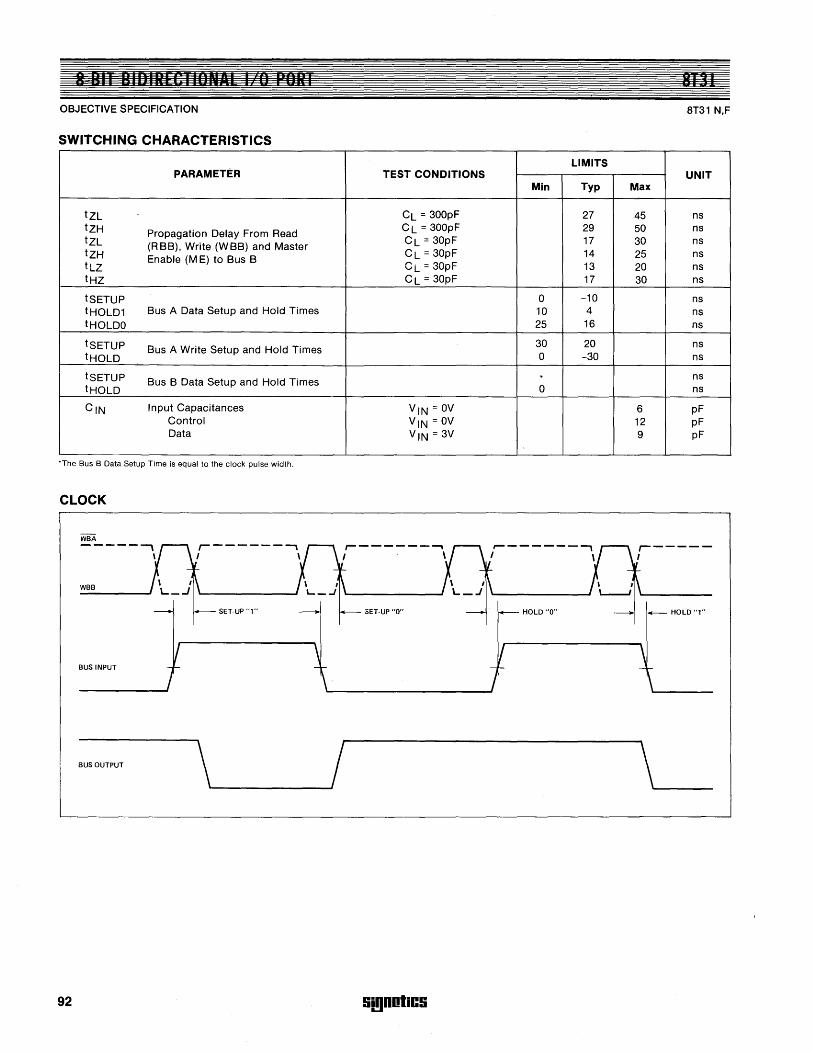
U F URT 8131
OBJECTIVE SPECIFICATION 8T31 N,F
SWITCHING CHARACTERISTICS
LIMITS PARAMETER TEST CONDITIONS UNIT
Min Typ Max
tZL CL = 300pF 27 45 ns tZH Propagation Delay From Read
CL = 300pF 29 50 ns tZL (RBB), Write (WBB) and Master CL=30pF 17 30 ns tZH Enable (M E) to Bus B CL = 30pF 14 25 ns tLZ CL = 30pF 13 20 ns tHZ CL = 30pF 17 30 ns
tSETUP 0 -10 ns tHOLD1 Bus A Data Setup and Hold Times 10 4 ns tHOLDO 25 16 ns
tSETUP Bus A Write Setup and Hold Times 30 20 ns
tHOLD 0 -30 ns
tSETUP Bus B Data Setup and Hold Times " ns tHOLD 0 ns
CIN Input Capacitances VIN = OV 6 pF Control VIN = OV 12 pF Data VIN = 3V 9 pF
'The Bus B Data Setup Time is equal to the clock pulse width.
CLOCK
BUS OUTPUT \\--------J/ \'"---
92 Si!lDOliCS
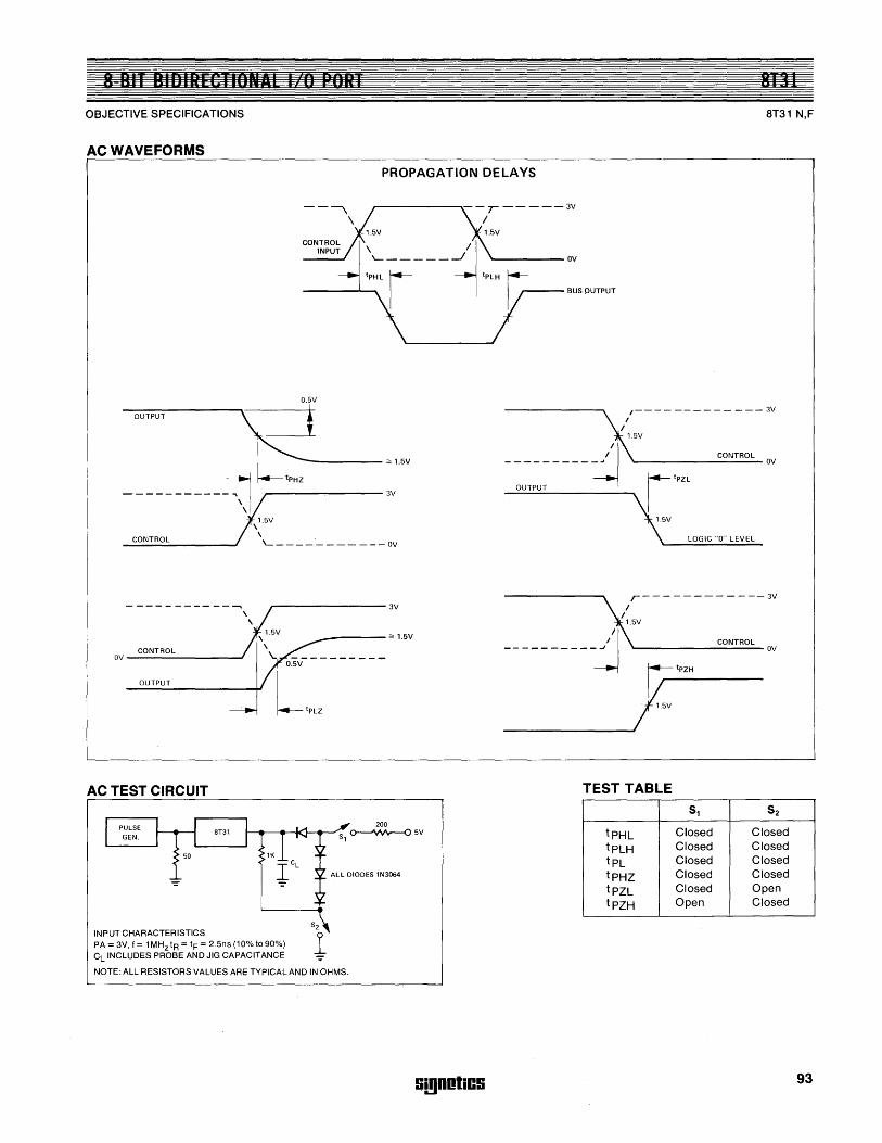
8 BIT BIDIRECTIONAL o PORI
OBJECTIVE SPECIFICATIONS
AC WAVEFORMS
PROPAGATION DELAYS
---------'---:~ -r-----/1 "~'H r- ov
~ 1 Ii 'US OUTPUT
O.5V
-------------.. r--------3V
\\/ <\..5V
CONTROL !'I < OV----------J
___ ----"".5V
OUTPUT
AC TEST CIRCUIT
200 r-'--'~3-.--r;Sl~5V
INPUT CHARACTERISTICS PA = 3V, f = 1 MHz tR = tF = 2.Sns (10% to 90%) CL INCLUDES PROBE AND JIG CAPACITANCE
ALL DIODES lN3064
NOTE: ALL RESISTORS VALUES ARE TYPICAL AND IN OHMS.
smDotiCS
TEST TABLE
tpHL tpLH tpL tpHZ tpZL tpZH
8T31
8T31 N,F
51 52
Closed Closed Closed Closed Closed Closed Closed Closed Closed Open Open Closed
93
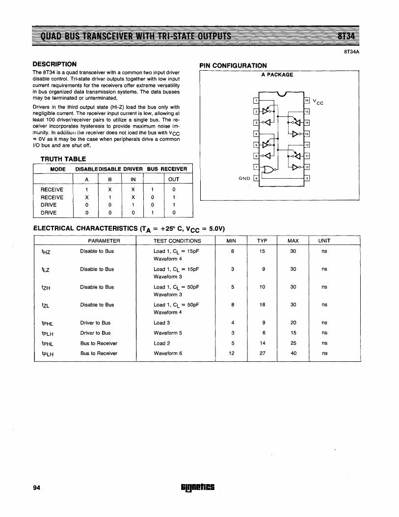
QUAD BUS IRANSliFIVEk Wll14 IAI STATE "II II*IITS
DESCRIPTION PIN CONFIGURATION The 8T34 is a quad transceiver with a common two input driver disable control. Tri-state driver outputs together with low input current requirements for the receivers offer extreme versatility in bus organized data transmission systems. The data b\.lsses may be terminated or unterminated.
Drivers in the third output state (Hi-Z) load the bus only with negligible current. The receiver input current is low, allowing at least 100 driver/receiver pairs to utilize a single bus. The receiver incorporates hysteresis to provide maximum noise immunity. In addition the receiver does not ioad the bus with VCC = OV as it may be the case when peripherals drive a common I/O bus and are shut off.
TRUTH TABLE
MODE DISABLE DISABLE DRIVER BUS RECEIVER
A B IN OUT
RECEIVE 1 X X 1 0
RECEIVE X 1 X 0 1
DRIVE 0 0 1 0 1
DRIVE 0 0 0 1 0
ELECTRICAL CHARACTERISTICS (T A = +250 C, VCC = 5.0V)
PARAMETER TEST CONDITIONS
tHZ Disable to Bus Load 1, CL = 15pF Waveform 4
tLZ Disable to Bus Load 1, CL = 15pF Waveform 3
tZH Disable to Bus Load 1, CL = 50pF Waveform 3
tZL Disable to Bus Load 1, CL = 50pF
Waveform 4
tpHL Driver to Bus Load 3
tpLH Driver to Bus Waveform 5
tpHL Bus to Receiver Load 2
tpLH Bus to Receiver Waveform 6
94 Sm1a'iDS
A PACKAGE
MIN TYP MAX
8 15 30
3 9 30
5 10 30
8 18 30
4 9 20
3 6 15
5 14 25
12 27 40
8T]4
8T34A
UNIT
ns
ns
ns
ns
ns
ns
ns
ns
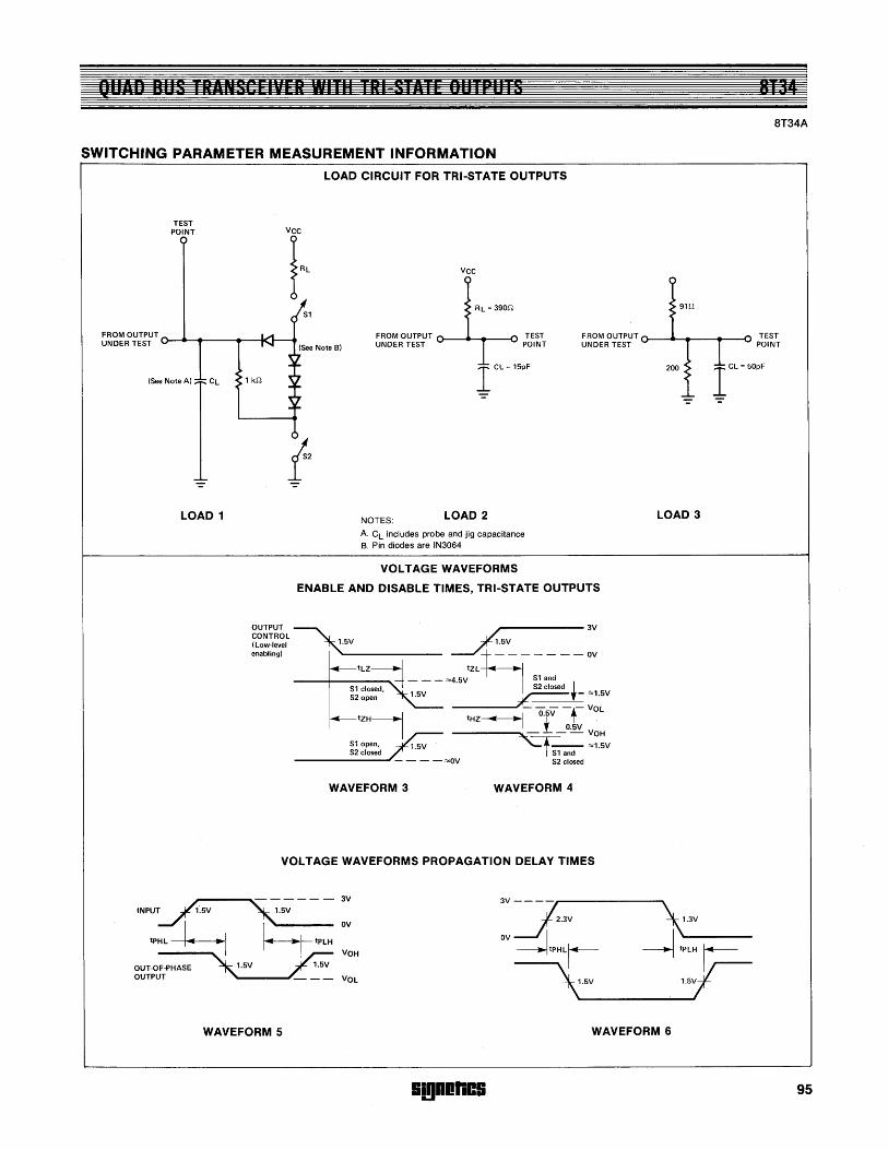
QUAD IUS TRANSCEIVER WITII TRI STATE DUTFU IS
SWITCHING PARAMETER MEASUREMENT INFORMATION
TEST POINT
LOAD CIRCUIT FOR TRI-STATE OUTPUTS
VCC
FROM OUTPUT UNDER TEST o-~-.--....... --KIJ--"'" JrL=390Q
FROM OUTPUT TEST UNDER TEST POINT
(See Note A) CL
-=
LOAD 1
I CL= 15pF
NOTES: LOAD 2
A. CL includes probe and jig capacitance B. Pin diodes are IN3064
VOLTAGE WAVEFORMS
ENABLE AND DISABLE TIMES, TRI-STATE OUTPUTS
OUTPUT~ ~3V CONTROL (Low-level t.5V 1.5V
enabling). - - - - - - - OV
__ -+ __ tL_Z------..j ___ ""4.5VtZL I S1 and
S1 I =d" -t S2 closed I S2 ~~:~ , 1.5V • - ""1.5V
tZHi
~1open, 1.5V S2 closed
-I 0.5\1 -t- VOL
------..l ' 0.5V V :>k~ - OH ''-t-- ""1.5V S1 and
----""OV S2 closed
WAVEFORM 3 WAVEFORM 4
VOLTAGE WAVEFORMS PROPAGATION DELAY TIMES
INPUT1.5V ~5~ - - - 3V
'PHL~ ~~LH:H OUT-O~ 1.5V ~ OUTP~~PHASE; ~ ~-~
VOL
9Hl
200
LOAD 3
WAVEFORM 5 WAVEFORM 6
smlOlies
8131
8T34A
I CL = 50pF
95
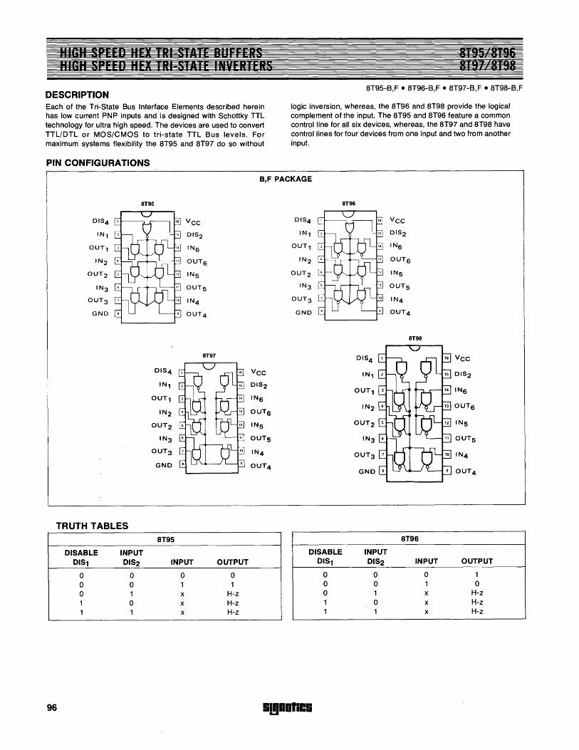
H 'Gil sp. f n II. X • k' STATr n" rrEkS lUSH SPEED HEX 181 STAlE INVERTERS
DESCRIPTION Each of the Tri-State Bus Interface Elements described herein has low current PNP inputs and is designed with Schottky TTL technology for ultra high speed. The devices are used to convert TTL/DTL or MaS/CMOS to tri-state TTL Bus levels. For maximum systems flexibility the 8T95 and 8T97 do so without
PIN CONFIGURATIONS
81" 8T 5
J 19. UI08
8T95-B,F. 8T96-B,F • 8T97-B,F • 8T98-B,F
logic inversion, whereas, the 8T96 and 8T98 provide the logical complement of the input. The 8T95 and 8T96 feature a common control line for all six devices, whereas, the 8T97 and 8T98 have control lines for four devices from one input and two from another input.
B,F PACKAGE
8T95
0154 ,
IN1 15 0152
OUT1 3 14 IN6
IN2 13 OUT6
OUT2 12 IN5
IN3 6 " OUT5
OUT3 10 IN4
GNO . 9 OUT4
8T97
015 4
IN1
OUT1
IN2
OUT2
IN3
OUT3
GNO
TRUTH TABLES 8T95
DISABLE INPUT DIS1 DIS2 INPUT
0 0 0 0 0 1 0 1 x 1 0 x 1 1 x
96
Vee
15 0152
14 IN6
13 OUT6
12 IN5
11 OUT5
OUT4
OUTPUT
0 1
H-z H-z H-z
0154
IN1
OUT1
IN2
OUT2
IN3
OUT3
GNO 8
DISABLE DIS1
0 0 0 1 1
SmODrilS
8T96
16 Vee
15 0152
14 INS
13 OUTS
IN5
" OUT5
OUT4
8T98
OUT1 3
GNO 8
8T96
INPUT DIS2 INPUT
0 0 0 1 1 x 0 x 1 x
13 OUTs
11 OUT5
OUTPUT
1 0
H-z H-z H-z
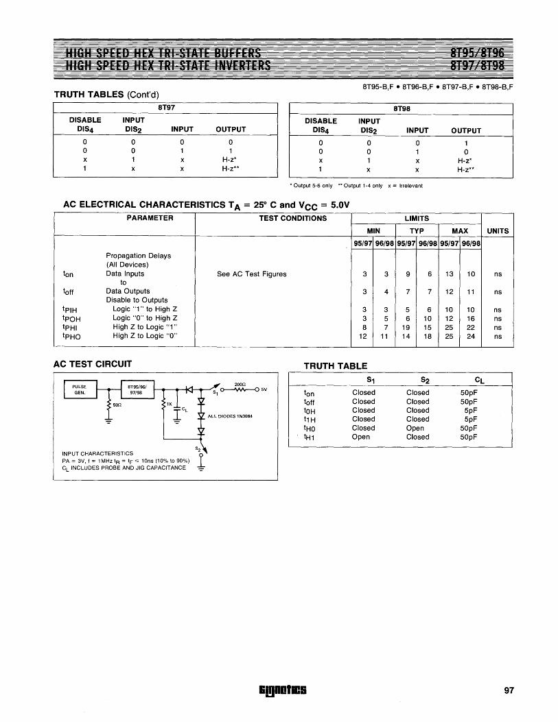
HIGH SPEED HEX Til STATE BIIFFERS 8195 RT91S HIGH SPEED HEX TRI STATE INVERTERS BT97 BT98
8T95-B,F • 8T96-B,F • 8T97-B,F .8T98-B,F TRUTH TABLES (Cont'd)
8T97 8T98
DISABLE INPUT DISABLE INPUT DIS4 DIS2 INPUT OUTPUT DIS4 DIS2 INPUT
0 0 0 0 0 0 0 0 0 1 1 0 0 1 x 1 x H-z* x 1 x 1 x x H-z** 1 x x
• Output 5-6 only" Output 1-4 only x = Irrelevant
AC ELECTRICAL CHARACTERISTICS T A = 250 C and V CC = 5.0V PARAMETER TEST CONDITIONS
MIN
95/97 96/98
Propagation Delays (All Devices)
ton Data Inputs See AC Test Figures 3 3 to
toft Data Outputs 3 4 Disable to Outputs
tplH Logic "1" to High Z 3 3 tpOH Logic "0" to High Z 3 5 tpHI High Z to Logic "1" 8 7 tpHO High Z to Logic "0" 12 11
AC TEST CIRCUIT TRUTH TABLE
2000 ........... .--...-Kl---.-~Sl Q-----AtI\IIr-- 5V ton
L...-_----J
INPUT CHARACTERISTICS PA = 3V. f = 1MHz 'R = tF ~ 10ns (10% to 90%) CL INCLUDES PROBE AND JIG CAPACITANCE
ALL DIODES lN3064
toft tOH t1 H tHO tH1
1~IDlill
S1
Closed Closed Closed Closed Closed Open
LIMITS
TYP
95/97 96/98
9 6
7 7
5 6 6 10
19 15 14 18
S2
Closed Closed Closed Closed Open Closed
OUTPUT
1 0
H-z* H-z**
MAX UNITS
95/97 96/98
13 10 ns
12 11 ns
10 10 ns 12 16 ns 25 22 ns 25 24 ns
CL
50pF 50pF
5pF 5pF
50pF 50pF
97
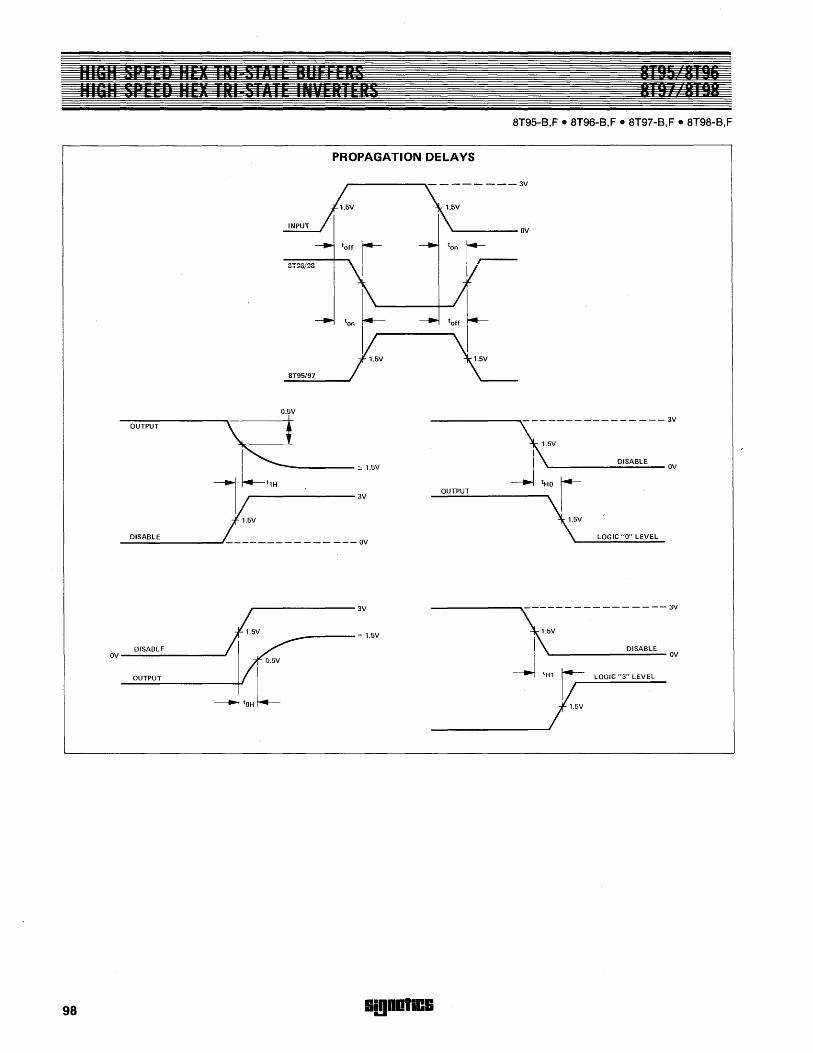
IIlrH SPEEn HEX IBI SI'I Itl ft t I DR 81 b 8T'" 111GB !H'EEH BEl I II 51' It IfIVElii EllS 819. 8ISP
8T95-8,F. 8T96-8,F • 8T97-8,F • 8T98-8,F
PROPAGATION DELAYS
1.5V
1.5V
8T95/97
~ 1
[:"" -~1.5V __ D_ISA_B_LE ________ ~~~5V----------_-_--_-_-_~
OUTPUT
juv 3V
\v - - ----- ---- 3V
'" 1.5V
DISABLE
J.",v= DISABLE
OV OV
OUTPUT
I LOGIC "3" LEVEL
tOH~ )I"
98
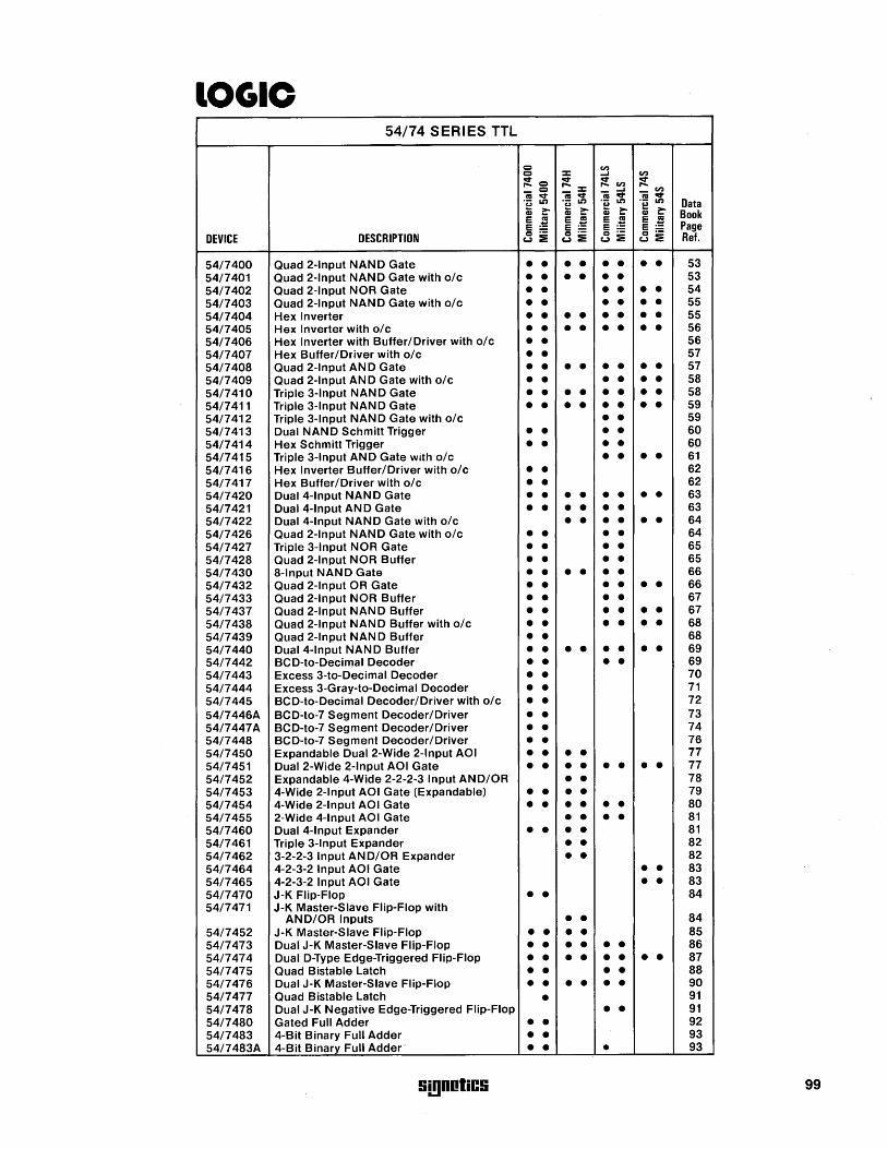
lOGIC
DEVICE
54/7400 54/7401 5411402 5411403 5411404 5411405 54/7406 5411407 5411408 5411409 54/7410 5411411 5411412 5411413 5411414 5411415 54/7416 5411417 5411420 5411421 54/7422 5411426 5411427 5411428 54/7430 5411432 5411433 54/7437 5411438 5411439 54/7440 54/7442 5411443 5411444 5411445 5411446A 5411447A 5411448 5411450 54/7451 5411452 5411453 54/7454 5411455 5411460 5411461 5411462 5411464 5411465 54/7470 5411471
5411452 5411473 5411474 5411475 54/7476 5411477 5411478 5411480 5411483 5411483A
54/74 SERIES TTL
DESCRIPTION
Quad 2-lnput NAND Gate Quad 2-lnput NAND Gate with o/c Quad 2-lnput NOR Gate Quad 2-lnput NAND Gate with o/c Hex Inverter Hex Inverter with o/c Hex Inverter with Buffer/Driver with o/c Hex Buffer/Driver with o/c Quad 2-lnput AN 0 Gate Quad 2-lnput AND Gate with o/c Triple 3-lnput NAND Gate Triple 3-lnput NAND Gate Triple 3-lnput NAND Gate with o/c Dual NAND Schmitt Trigger Hex Schmitt Trigger Triple 3-lnput AND Gate with o/c Hex Inverter Buffer/Driver with o/c Hex Buffer/Driver with o/c Dual 4-lnput NAND Gate Dual 4-lnput AND Gate Dual 4-lnput NAND Gate with o/c Quad 2-lnput NAND Gate with o/c Triple 3-lnput NOR Gate Quad 2-lnput NOR Buffer 8-lnput NAN 0 Gate Quad 2-lnput OR Gate Quad 2-lnput NOR Buffer Quad 2-lnput NAND Buffer Quad 2-lnput NAND Buffer with o/c Quad 2-lnput NAN 0 Buffer Dual 4-lnput NAN 0 Buffer BCD-to-Decimal Decoder Excess 3-to-Decimal Decoder Excess 3-Gray-to-Decimal Decoder BCD-to-Decimal Decoder/Driver with o/c BCD-to-7 Segment Decoder/Driver BCD-to-7 Segment Decoder/Driver BCD-to-7 Segment Decoder/Driver Expandable Dual 2-Wide 2-lnput AOI Dual 2-Wide 2-lnput AOI Gate Expandable 4-Wide 2-2-2-3 Input AND/OR 4-Wide 2-lnput AOI Gate (Expandable) 4-Wide 2-lnput AOI Gate 2-Wide 4-lnput AOI Gate Dual 4-lnput Expander Triple 3-lnput Expander 3-2-2-3 Input AND/OR Expander 4-2-3-2 Input AOI Gate 4-2-3-2 Input AOI Gate J-K Flip-Flop J-K Master-Slave Flip-Flop with
AND/OR Inputs J-K Master-Slave Flip-Flop Dual J-K Master-S!ave Flip-Flop Dual D-Type Edge-Triggered Flip-Flop Quad Bistable Latch Dual J-K Master-Slave Flip-Flop Quad Bistable Latch Dual J-K Negative Edge-Triggered Flip-Flop Gated Full Adder 4-Bit Binary Full Adder 4-Bit Binary Full Adder'
!i!!lDotiC!i
• • • • • • • • • • • • • • • • • • • • • • • • • • • • • • • • • • • • • • • • • • • • • • • • • • • • • • • • • • • • • • • • • • • • • • • • • • • • • • • •
• •
• • • • • • • • • • •
• • • • • •
• • • •
• • • •
• • • • • •
• • • • • •
• •
• •
• • • • • • • • • • • • • • • • • •
• • • • • • • • • •
• • • • • • • • • • • •
• • • • • • • • • • • • • • • •
• • • • • • • • • • • • • ••
• •
• • • •
• • • • • • • • • •
•
• • • • • • • • • •
• • • • • • • •
• •
• • • •
• • • • • • • •
• •
• • • •
• •
Data Book Page Ref.
53 53 54 55 55 56 56 57 57 58 58 59 59 60 60 61 62 62 63 63 64 64 65 65 66 66 67 67 68 68 69 69 70 71 72 73 74 76 77 77 78 79 80 81 81 82 82 83 83 84
84 85 86 87 88 90 91 91 92 93 93
99
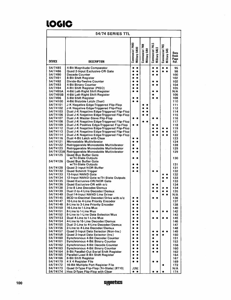
100
lOGIC
DEVICE
54/7485 54/7486 54/7490 54/7491 54/7492 54/7493 54/7494 54/7495A 54/7495B 54/7496 54/74100 54/74101 54/74102 54/74103 54/74106 54/74107 54/74108 54/74109 54/74112 54/74113 54/74114 54/74116 54/74121 54/74122 54/74123 54/74123A 54/74125
54/74126
54/74128 54/74132 54/74133 54/74134 54/74135 54/74136 54/74138 54/74139 54/74140 54/74145 54/74147 54/74148 54/74150 54/74151 54/74152 54/74153 54/74154 54/74155 54/74156 54/74157 54/74158 54/74160 54/74161 54/74162 54/74163 54/74164 54/74165 54/74166 54/74170 54/74172 54/74173 54/74174
54/74 SERIES TTL
DESCRIPTION
4-Bit Magnitude Comparator Quad 2-lnput Exclusive-OR Gate Decade Counter 8-Bit Shift Register Divide-By-Twelve Counter 4-Bit Binary Counter 4-Bit Shift Register (PI SO) 4-Bit Left-Right Shift Register 4-Bit Left-Right Shift Register 5-Bit Shift Register 4-Bit Bistable Latch (Dual) J-K Negative Edge-Triggered Flip-Flop J-K Negative Edge-Triggered Flip-Flop Dual J-K Negative Edge-Triggered Flip-Flop Dual J-K Negative Edge-Triggered Flip-Flop Dual J-K Master-Slave Flip-Flop Dual J-K Negative Edge-Triggered Flip-Flop Dual J-K Positive Edge-Triggered Flip-Flop Dual J-K Negative Edge-Triggered Flip-Flop Dual J-K Negative Edge-Triggered Flip-Flop Dual J-K Negative Edge-Triggered Flip-Flop Dual 4-Bit Latch with Clear Monostable Multivibrator Retriggerable Monostable Multivibrator Retriggerable Monostable Multivibrator Retriggerable Monostable Multivibrator Quad Bus Buffer Gate
w/Tri-State Outputs Quad Bus Buffer Gate
w/Tri-State OutPUtS Quad ~-Input NOR Buffer Quad Schmitt Trigger 13-lnput NAND Gate 12-lnput NAND Gate w/Tri-State Outputs Quad Exclusive-OR/NOR Gate Quad Exclusive-OR with o/c 3-to-8 Line Decoder/Demux Dual 2-to-4 Line Decoder/Demux Dual 14-lnput NAND Line Driver BCD-to-Decimal Decoder/Drive with o/c 10-Line to 4-Line Priority Encoder 8-Line to 3-Line Priority Encoder 16-Line to 1-Line Mux 8-Line to 1-Line M ux 8-Line to 1-Line Data Selector/Mux Dual 4-Line to 1-Line Mux 4-Line to 16-Line Decoder/Demux Dual 2-Line to 4-Line Decoder/Demux 2-Line to 4-Line Decoder/Demux Quad 2-lnput Data Selector (Non-Inv.) Quad 2-lnput Data Selector (Inv.) Synchronous 4-Bit Decoder Counter Synchronous 4-Bit Binary Counter Synchronous 4-Bit Decade Counter Synchronous 4-Bit Binary Counter 8-Bit Parallel-Out Serial Shift Register Parallel-Load 8-Bit Shift Register 8-Bit Shift Register 4 X 4 Register File 16-Bit Multiple Port Register File Quad D-Type Flip-Flop (Tri-State) (8T10) Hex D-Type Flip-Flop with Clear
S!!IDOliCS
• • • • • • • • • • • • • • • • • • • •
• • • •
• • • • • • • • • • • • • • • • •
• • • • • • • • • • • • • • • • • • • • • • • • • • • JUNE • •
• • • • • • • • • •
• • • • • • • • • • • • • • •
• • • • • • • • • •
• •
• • • • • • • •
• • • •
• • • • • • • • • • • • •
• •
• •
• • • •
• • • • • •
It •
• • .. tt •
• • • •
., . • •
• • •
• •
Data Book Page Ref.
95 98
100 102 102 104 105 N/A 106 108 110 111 112 114 115 116 117 118 119 121 122 123 124 128 129 129
130
131 131 132 132 133 133 134 134 135 N/A 136 137 138 140 142 143 145 146 147 148 149 150 151 153 156 160 162 164 167 169 172 N/A 174
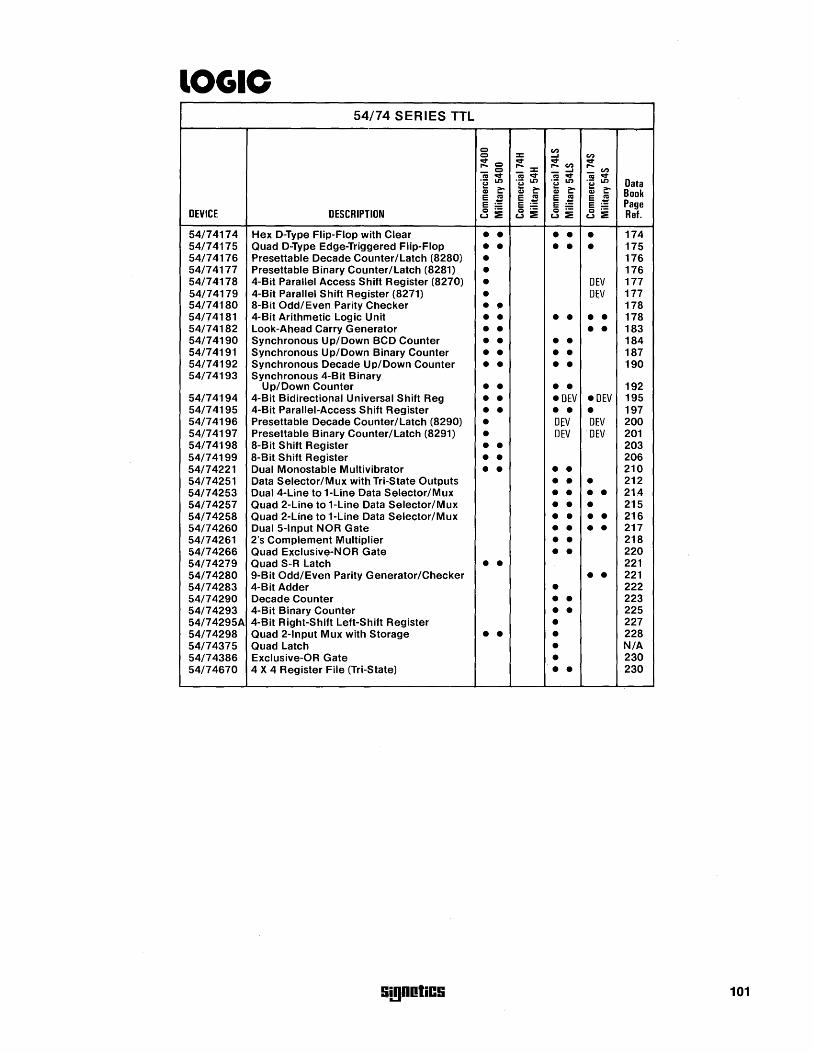
lOGIC 54/74 SERIES TTL
DEVICE DESCRIPTION
54174174 Hex D-Type Flip-Flop with Clear • 54/74175 Quad D-Type Edge-Triggered Flip-Flop • 54174176 Presettable Decade Counter/Latch (8280) 54174177 Presettable Binary Counter/Latch (8281) 54174178 4-Bit Parallel Access Shift Register (8270) 54174179 4-Bit Parallel Shift Register (8271) 54174180 8-Bit Odd/Even Parity Checker • 54/74181 4-Bit Arithmetic Logic Unit • 54174182 Look-Ahead Carry Generator • 54174190 Synchronous Up/Down BCD Counter • 54/74191 Synchronous Up/Down Binary Counter • 54174192 Synchronous Decade Up/Down Counter • 54174193 Synchronous 4-Bit Binary
Up/Down Counter •• 54174194 4-Bit Bidirectional Universal Shift Reg •• 54/74195 4-Bit Parallel-Access Shift Register •• 54174196 Presettable Decade Counter/Latch (8290) • 54174197 Presettable Binary Counter/Latch (8291) • 54174198 8-Bit Shift Register •• 54174199 8-Bit Shift Register •• 54174221 Dual Monostable Multivibrator •• 54174251 Data Selector/Mux with Tri-State Outputs 54174253 Dual 4-Line to 1-Line Data Selector/Mux 54174257 Quad 2-Line to 1-Line Data Selector/Mux 54174258 Quad 2-Line to 1-Line Data Selector/Mux 54174260 Dual 5-lnput NOR Gate 54174261 2's Complement Multiplier 54174266 Quad Exclusive-NOR Gate 5417 4279 Quad S-R Latch • • 54174280 9-Bit Odd/Even Parity Generator/Checker 54174283 4-Bit Adder 5A17 4290 Decade Counter 54174293 4-Bit Binary Counter 54174295A 4-Bit Right-Shift Left-Shift Register 54174298 Quad 2-lnput Mux with Storage •• 54174375 Quad Latch 5417 4386 Exclusive-OR Gate 54174670 4 X 4 Register File (Tri-State)
S!!IDotiCS
Data Book Page Ref.
••• 174 ••• 175
176 176
DEV 177 DEV 177
178 •• •• 178
•• 183
• • 184 • • 187 • • 190
• • 192 .DEV .DEV 195 ••• 197 DEV DEV 200 DEV DEV 201
203 206
• • 210 ••• 212 •• •• 214 ••• 215 •• •• 216 •• •• 217
• • 218 • • 220
221 •• 221
• 222 • • 223 • • 225 • 227 • 228 • N/A • 230 • • 230
101
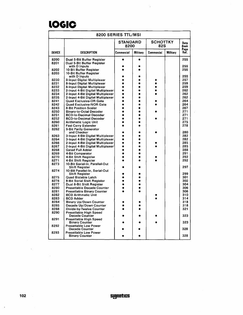
lOGIC 8200 SERIES TTL/MSI
STANDARD SCHOTTKY Data 8200 82S Book
Page DEVICE DESCRIPTION Commercial Military Commercial Military Ref.
8200 Dual 5-Bit Buffer Register • • 255 8201 Dual 5-Bit Buffer Register
with D Inputs • • 255 8202 10-Bit Buffer Register • • 255 8203 10-Bit Buffer Register
with D Inputs 255 0""'1"\ o,-'v 8-lnput Digital Multiplexer • 257 8231 8-lnput Digital Multiplexer • 259 8232 8-lnput Digital Multiplexer • 259 8233 2-lnput 4-Bit Digital Multiplexer • 262 8234 2-lnput 4-Bit Digital Multiplexer • 262 8235 2-lnput 4-Bit Digital Multiplexer 262 8241 Quad Exclusive-OR Gate • 264 8242 Quad Exclusive-NOR Gate • 264 8243 8-Bit Position Scaler 267 8250 Binary-to-Octal Decoder • 271 8251 BCD-to-Decimal Decoder 271 8252 BCD-to-Decimal Decoder • 271 8260 Arithmetic Logic Unit 275 8261 Fast Carry Extender 278 8262 9-Bit Parity Generator
and Checker • • • 280 8263 3-lnput 4-Bit Digital Multiplexer • • 282 8264 3-lnput 4-Bit Digital Multiplexer • • 282 8266 2-lnput 4-Bit Digital Multiplexer • • • 285 8267 2-lnput 4-Bit Digital Multiplexer • • • 285 8268 Gated Full Adder • • 288 8269 4-Bit Comparator • • 291 8270 4-Bit Shift Register • • • 292 8271 4-Bit Shift Register • • • 292 8273 10-Bit Serial-In, Parallel-Out
Shift Register • • 297 8274 10-Bit Parallel-In, Serial-Out
Shift Register • • 299 8275 Quad Bistable Latch • • 301 8276 8-Bit Serial Shift Register • • 302 8277 Dual 8-Bit Shift Register • • 304 8280 Presettable Decade Counter • • 306 8281 Presettable Binary Counter • • 306 8282 BCD Arithmetic Unit • 310 8283 BCD Adder • 314 8284 Binary Up/Down Counter • • 318 8285 Decade Up/Down Counter • • 318 8288 Divide-by-Twelve Counter • • 321 8290 Presettable High Speed
Decade Counter • • • 323 8291 Presettable High Speed
Binary Counter • • • 323 8292 Presettable Low Power
Decade Counter • • 328 8293 Presettable Low Power
Binary Counter • • 328
102 !ii!lDotiC!i
LOGIC FUNCTION SELECTOR GUIDES
Use these charts to quickly identify the most suitable devices to meet your system needs. The following charts group together similar function circuits in Signetics TTL families.
ARITHMETIC UNITS/MICROPROCESSOR CPUs
!:::: ::::l t..:I a::
en t3 l- e ::::l c... <:
en ~
LoU l- I- :: ai l- I- ::::l <:
Ll- z: ::::l c... ::..:: e LoU c... l- e
:E I- ::::l e ~ a:: LoU ::::l e ....J LoU ....J e >- >- >-CD c... a:: a:: a:: :E :E :E a:: a:: a::
FUNCTION DEVICE ::::l e ::::l <: <: <: z: t..:I en t..:I t..:I t..:I
ALU (BINARY) 8260 4 74181 4 74S181 4 74LS181 ,4
ALU (BCD) 82S82 4
GATED FULL ADDER 8268 2 X X X (BINARY) 7480 2 X X X
7483 4 X X X 74S83 4 X X X 74S283 4 X X X X
GATED FULL ADDER (BCD) 82S83 4 X X X X
LOOK-AHEAD CARRY 8261 (Extender) 4
74182 4 74S182 4
2's COMPLEMENT MULTIPLIER 74LS261 2x4
smAoties 103
DATA SELECTOR/MULTIPLEXER I--::=l e... I--::=l 0
I--t.::I
I-- t...:I z: ....J CI:) u.J I-- i= ::=l 0 ....J ::=l e... a:: I-- u.J
CI:) a:: I-- ::=l CI:) I--
e... u.J ::=l I-- e... ::=l
I-- I-- :> 0 I-- I-- z: §: - CI:) I-- I--
::=l z: ::=l 0 =. ::=l z: e... 0 ::=l a:: ::=l e... t...:I I--0 u.J I-- e... Z 0 e... I-- I-- u.J ::=l
~ ::=l t.::I I-- I-- I-- I-- u.J Qj § u.J ....J e... a:: 0 z: ::=l 0
t...:I ::=l ::=l 0 co co I-- u.J u.J
i= 0 z: u.J 0 0 Q :i: :::z::: 0 u.I cz:: ::=l I--
....J L.L ........ u.I ....J 0 ~ ~ ~ a:: z: z: 0 t:
e... 0 a:: t.::I t.::I 0 u.J :::J u.I ~ u.I z: z: 0 0
....J I-- a:: 0 I-- 0 0 ~ a:: :> 0 cz:: I-- I-- CI:) I-- 0 u.I i= i= u.I ~ t...:I cz:: u.I I-- u.I u.I u.I t...:I co ~ a:: a:: :::.::: I-- 0 0 ::=l ::=l I-- t...:I ::=l :::z::: :::z:::
t...:I c z: CJ? z: 0 e... e... ::=l u.I e... t...:I t...:I z: cz:: ~ Z u.J u.I
0 ....J u.I cz:: t...:I I-- I-- ....J I-- I-- I-- u.I I--::=l 0 :> :>
....J 0 e... ii: I-- z: ::=l ::=l e... u.I ::=l cz:: cz:: e... cz:: FUNCTION DEVICE z: z: ~ ~ t...:I :::z::: 0 I-- CI:) u.I 0 0 ~ CI:) 0 ....J ....J 0 c
SINGLE 8-INPUT MUL TIPLEXER 82301 82S30 2 X X X X
8231/82S31 2 X X X X X 8232/82S32 2 X X X X X 74151 2 X X X X X 74LS151 2 X X X X X 74S151 2 X X X X X 74152 1 X X X X 74LS251 2 X X X X X 74S251 2 X X X X X 9312 2 X X X
SINGLE 16-INPUT MULTIPLEXER 74150 1 X X X
DUAL4-INPUT MUL TlPLEXER 74153 2 X X X X X
74LS153 2 X X X X X 74S153 2 X X X X X 74LS253 2 X X X X 74S253 2 X X X X 9309 2 X X X
QUAD 2-INPUT MUL TIPLEXER 8233/82S33 4 X X X X
8234/82S34 4 X X X X 8235 4 X X X X 82661 82S66 4 X X X X 8267/82S67 4 X X X X 74157/74S157 4 X X X X X 74158/74S158 4 X X X X X 74S257 4 X X X X 74S258 4 X X X X 74298 4 X j X X X X
(w I storage)
QUAD3-INPUT MUL TIPLEXER 8263 4 X X X X
8264 4 X X X X X X
104 Si!lDotiCS
COUNTERS
in ...J ::..:::
e §: 0 u - e c:: 0 ...J I-- I-- ...J 0 UoI I-- I-- I-- I-- z: U c:: en UoI UoI UoI UoI I-- 0 z: I--
en UoI en en en en UoI z: c:: c:: UoI UoI UoI UoI en Cl:I u 3: 0 UoI UoI
Cl:I I-- 0.. c:: c:: c:: c:: UoI z: z: 0 U I--< c:: z: en 0.. en en en c:: a: 3: 0 :::l I-- UoI :::l :::l en :::l :::l :::l en UoI ........ UoI UoI 0.. en 0 0.. ...J 0 I-- CLOCK c:: I-- 0 0 :::l 0 0 0 :::l Cl:I 0 :::l CD I-- 0 :::l L.L. UoI z: u z: 0 z: z: z: 0 Cl:I ........ < I-- :::l ::!E 0 I-- :::l 0 z: 0 0 0 z: a: 0.. UoI z: :::l 0 0 FREQUENCY z: c:: z: 0
3: c:: 0 c:: c:: c:: 0 I-- :::l I-- UoI ~ 0 3: c 0
:::l U ::z:: c:: ::z:: ::z:: ::z:: c:: UoI < UoI UoI (MHz) UoI 0 u ::z:: u u u ::z:: ::..::: c:: I-- >- >- 0 0 0
CD 0 z: 0 z: u z: z: z: u U ...J < z: c:: c:: c:: 0 0
::!E u 3: ........ >- z: >- >- >- z: 0 Cl:I
0.. :::l c:: c:: c:: u U :::l 0.. C 0.. en >- en en en >- ...J z: UoI 0 < < 0 z: UoI
FUNCTION DEVICE z: :::l C :::l < en < < < en u en en u u u CD UoI c Min Typ Max
RIPPLE BINARY COUNTER 8281/74197 4 X X X I 20 25
8291 4 X X X j 40 60 82S91 4 X X X I 85 100 8293 4 X X X j 5 10 7493 4 X X 1 X 10 18 74LS93 4 X X 1 X 32 74LS197 4 X X X I 15
RIPPLE DECADE COUNTER 8280174176 4 X X X I 20
8290 4 X X X I 40 60 82S90 4 X X X j 85 100 8292 4 X X X I 5 7490 4 X X X I 10 74LS90 4 X X X j 30 74LS196 4 X X X I 30 74S196 4 X X X I 85 100
RIPPLE DIVIDE BY 12 COUNTER 8288 4 X X X I 20 25
7492 4 X X I X 10 74LS92 4 X X I X 16
SYNCHRONOUS BINARY COUNTER 8284 4 X X X I X X X X 20 30
74161 4 X X X I X X 25 74LS161 4 X X X 1 X X 25 74163 4 X X X 1 X X 25 74LS163 4 X X X 1 X X 25 74191 4 X X 1 X X X X X 20 25 74LS191 4 X X 1 X X X X X 20 74193 4 X X X 1 X X X 25 32 74LS193 4 X X X 1 X X X 25
SYNCHRONOUS DECADE COUNTER 8285 4 X X X X I X X X X 20 30
74160 4 X X X 1 X X 25 74LS160 4 X 74162 4 X X X 1 X X 25 74LS162 4 X X X 1 X X 25 74190 4 X X 1 X X X X X 20 74LS190 4 X X 1 X X X X X 20 25 74192 4 X X X 1 X X X 25 74LS192 4 X X X 1 X X X 25
Gi!lDOliCG 105
DECODERS/DEMUL TIPLEXERS
ell ell I--
I-- ~ ~ ell ell e.. I--
<' L.U e.. I-- L.U I-- I-- ~ e c.::J I-- ell
~ ....J ~ ~ e.. L.U
.§.. c:c ~ ell I-- e.. cc e.. e ~ e ....J I-- e I-- ~ c:c I-- ell L.U
<' ell ....J ~ e.. ~ :z ~ I-- e.. c.::J ....J L.U
.§.. L.U e a:: e.. I-- L.U e ~ ~ I-- e t.:I :;:.. e I-- ~ e ......... e.. ....J :z
~ L.U e
a:: I-- e :::::; L.U a:: I-- ....J :;:: e.. e %: ~ I-- t.:I ~ cc L.U e I--:z ~
~ L.U e ;: c:c e I-- ~ ~ :z ~ :z c:c Ci) e e.. ....J :;:.. a:: I-- e e.. c:c I-- c:c t.:I
ell e e ~ ....J c.::J ell I-- ....J a:: I-- iE e a::
I-- I-- ~ e c:c ....J ell L.U e cc :z L.U :z :z
~ ~ e t.:I e L.U I-- L.U I-- I-- L.U :;:: I-- e e ell e.. e.. :z :z :;:.. iii I-- :z a:: ell ....J :z e.. :E :E e.. I-- I-- %: L.U c:c i= ;: ~
L.U L.U Ci) e.. c:c :E :E :E :E c.::J e.. :;:.. e..
FUNCTION DEVICE ~ ~ ;: e.. I-- t.:I ~ ~
e.. ~
L.U a: ....J c:c e e c:c e e e ell c:c e a:: cc ....J t.:I t.:I ....J
BCD TO 7-SEGMENT DECODER/DRIVER 8T04 40 X X X X X
8T05 2.3 X X X X X 8T06 40 X X X X X 7446 20 30 X X X X 7447 20 15 X X X X X X 7448 6.4 X X X X X
BINARY TO OCTAL DECODER/ 8250/82S50 X X X DEMULTIPLEXER
2-LlNE TO 4-LlNE DECODER/ 74LS139 (Dual) X X X DEMULTIPLEXER 74S139 (Dual) X X X
74155 (Dual) X X X 74156 (Dual) X X X
3-LlNE TO 8-LlNE DECODER/ 74LS138 X X X DEMULTIPLEXER 74S138 X X X
4-LlNE TO 16-LlNE 74154 X X X X DECODER/ DEMULTIPLEXER
EXCESS 3-TO-DECIMAL 7443 X X X DECODER
EXCESS 3-GRA Y-TO DECIMAL 7444 X X X DECODER
106 SmDOliCS
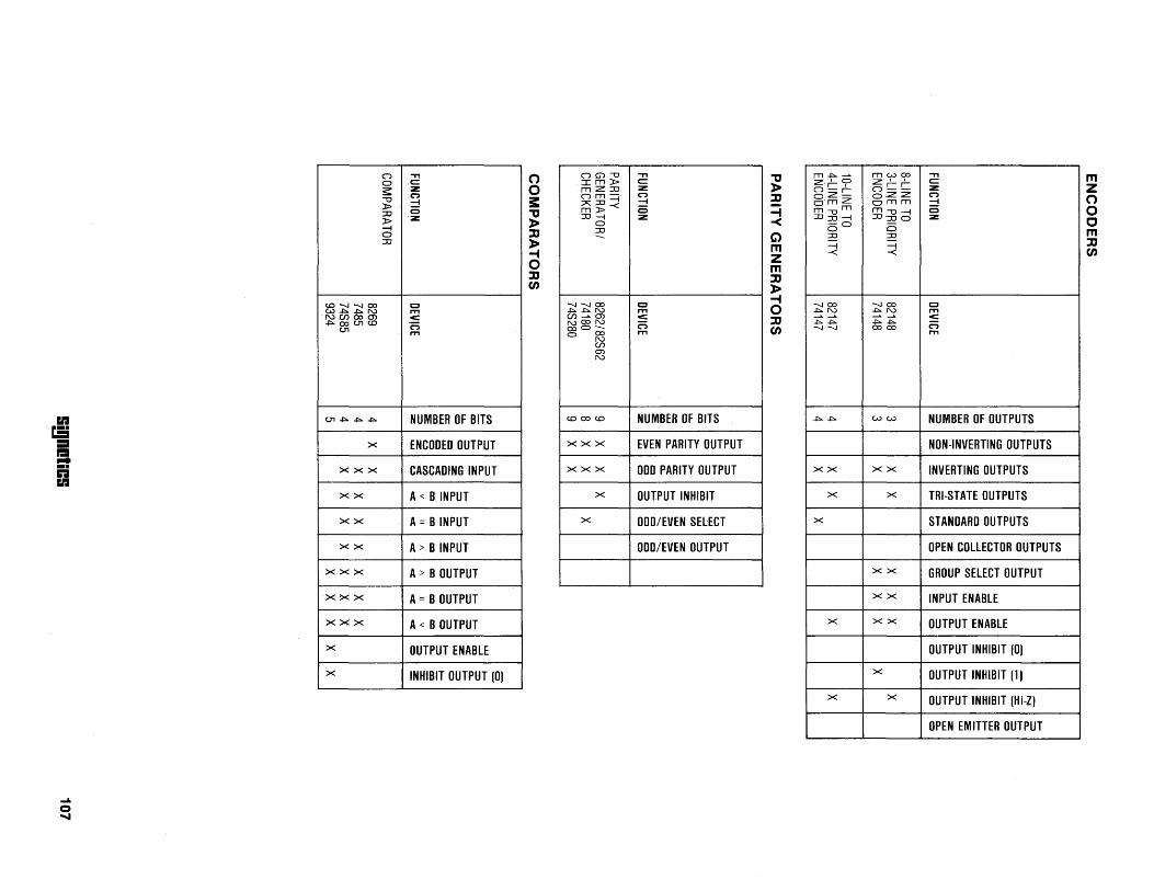
III t!i = 1':1 ... f.i III
-" o ......
C") 0 :s: -U » ::JJ » -I 0 ::JJ
c.o -..J -..J 0::> W':::"':::"I'\)
. I'\) .Cf) 0::> en .:::..o::>c..nc.o
c..n
c..n.:::...:::.. .:::..
x
xxx
xx
xx
xx
xxx
xxx
xxx
x
x
.,., .C::: z:
.C":I -I C z:
C rn c:: 'n rn
NUMBER OF BITS
ENCODED OUTPUT
CASCADING INPUT
A < B INPUT
A = B INPUT
A> B INPUT
A> B OUTPUT
A =B OUTPUT
A < B OUTPUT
OUTPUT ENABLE
INHIBIT OUTPUT (0) - --
o o 3C "tJ » :rJ » -i o J:'J en
C") G') -U :::r::m» m2:::JJ
Rgj=i m»-< ::JJ -I
0 ::JJ --
-..J -..J 0::> ':::"':::"1'\) Cf) ...... en NO::> I'\) 0::>0--o 0::> I'\)
Cf) en I'\)
c.o 0::> c.o
xxx
xxx
x
x
- '--
.,., ! c:::
z: C":I -I C :z:
!
C rn c:: n rn
NUMBER OF BITS
EVEN PARITY OUTPUT
ODD PARITY OUTPUT
OUTPUT INHIBIT
ODD/EVEN SElECT
ODD/EVEN OUTPUT
"tJ » J:'J =i -< C) m Z m J:'J » -i o J:'J en
m.:::..--" 2:.' 0 C")!::r-02:-c,m2: m-u m ::JJ::JJ-I
6 0
::JJ =i -<
-..J 0::> ':::"1'\)
.:::.. .:::.. -..J -..J
.:::.. .:::..
xx
x
x
x
x
m W 0::> 2:' , C")!::!:: 0·2:2: omm m-U-l ::JJ'~0
0 ::JJ =i -<
-..J 0::> ':::"1'\) .--" --" .:::.. .:::.. 0::> 0::>
ww
xx
x
xx
xx
xx
x
x
.,., c::: :z: C":I -I C :z:
C rn c:: n m
NUMBER OF OUTPUTS
NON-INVERTING OUTPUTS
INVERTING OUTPUTS
TRI-STATE OUTPUTS
STANDARD OUTPUTS
OPEN COLLECTOR OUTPUTS
GROUP SHECT OUTPUT
INPUT ENABLE
OUTPUT ENABLE
OUTPUT INHIBIT (0)
OUTPUT INHIBIT (1)
OUTPUT INHIBIT (Hi-Z)
OPEN EMITTER OUTPUT
J
m Z o o C m J:'J en
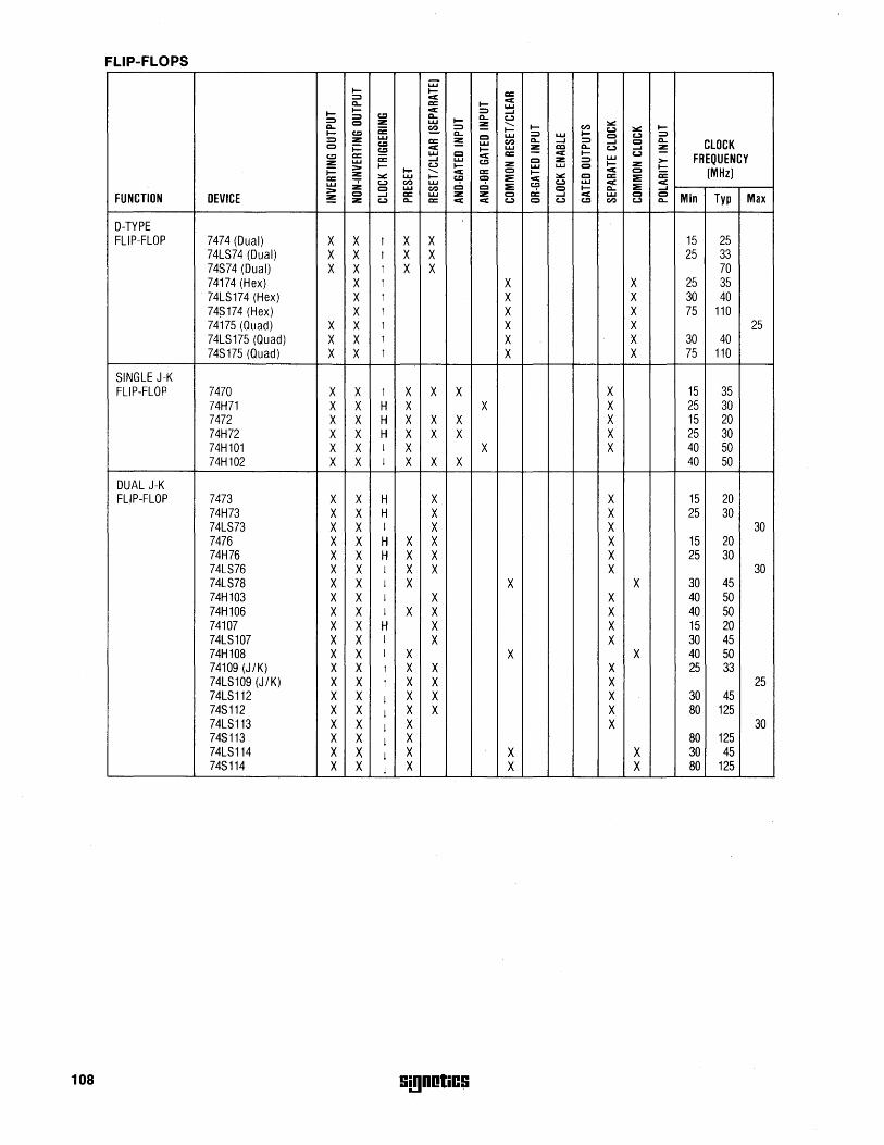
FLIP-FLOPS u::;
~ ~ a:: ::;) < a.. a:: ~ < I,U
~ ~ < ::;) ...J ::;) c:::I a.. a.. u ::;) Q z: LU ~
~ "- ~ a.. a: ~ ::;) ~ ~ CI:) U ~ ~
~ t:l LU
a.. Q I,U ::;) LU ~ Q CU ::;)
=> z: c:::I a:: ::!!: LU CI:) a.. ...J ::;) ...J Q a.. CLOCK Q j:; c:::I < ~ LU ::!!: CD a.. u ....I !:
c:::I a:: a: ~ Q < a:: < ~ I,U
u FREQUENCY LU Q z: ::;) >-z: LU ~ U ...... c:::I z: LU LU Q ~ :z: ~
~ :> ~ "- < a:: Q ~ < Q (MHzl a:: ::!!: ~ LU ~ c:::I Q :E < ~ Q a:: :E a: LU Z: U CI:) LU 6 6 :E c:::I U LU < :E < :> Q LU CI:) c:f: Q ~ c:.. ....I
FUNCTION DEVICE !: Q ...J a:: LU z: z: Q ...J < I,U Q Q Min Typ Max z: u a.. a:: < < U Q U c:::I CI:) u a..
D-TVPE FLIP-FLOP 7474 (Dual) X X I X X 15 25
74LS74 (Dual) X X I X X 25 33 74S74 (Dual) X X I X X 70 74174 (Hex) X I X X 25 35 74LS174 (Hex) X I X X 30 40 74S174 (Hex) X I X X 75 110 74175 (Quad) X X I X X 25 74LS175 (Quad) X X I X X 30 40 74S175 (Quad) X X I X X 75 110
SINGLE J-K FLIP-FLOP 7470 X X I X X X X 15 35
74H71 X X H X X X 25 30 7472 X X H X X X X 15 20 74H72 X X H X X X X 25 30 74H101 X X j X X X 40 50 74H102 X X j X X X 40 50
DUAL J-K FLIP-FLOP 7473 X X H X X 15 20
74H73 X X H X X 25 30 74LS73 X X j X X 30 7476 X X H X X X 15 20 74H76 X X H X X X 25 30 74LS76 X X j X X X 30 74LS78 X X j X X X 30 45 74H103 X X j X X 40 50 74H106 X X j X X X 40 50 74107 X X H X X 15 20 74LS107 X X j X X 30 45 74H108 X X j X X X 40 50 74109 (J/K) X X I X X X 25 33 74LS109 (J/K) X X I X X X 25 74LS112 X X j X X X 30 45 74S112 X X j X X X 80 125 74LS113 X X j X X 30 745113 X X j X 80 125 74LS114 X X j X X X 30 45 74S114 X X j X X X 80 125
108 Si!lDotiCS
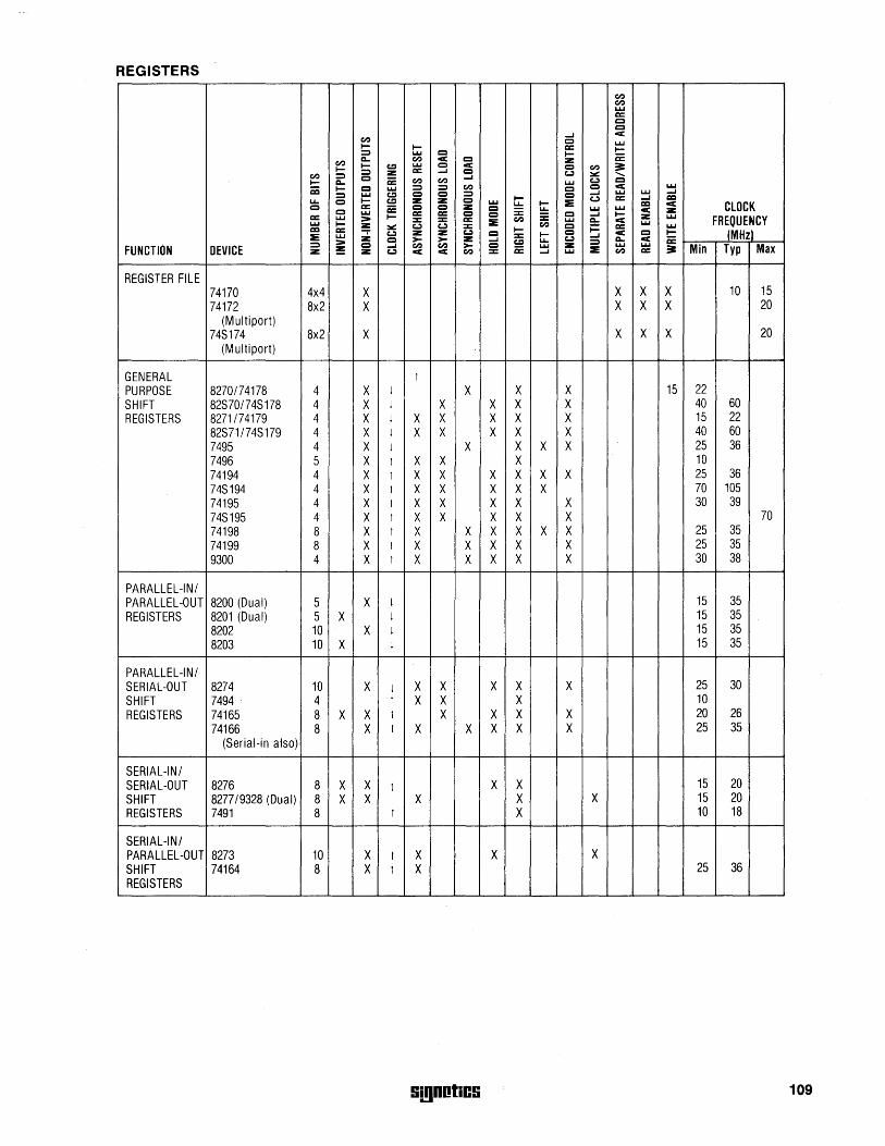
REGISTERS
en en L.LJ a: e e
en ....J < ~ ~
C L.LJ :::::) L.LJ C
a: ~ ~ a: en CI.. en < c :z
~ ~ ~ L.LJ C < C en ~
en :::::) :::::) :z a: ....J e '"' :.:: ........ e ....J
~ CI.. a: en en L.LJ '"' e iii ~ C L.LJ :::::) :::::) en c e < L.LJ
:::::) L.LJ ~ C C :::::) e ....J L.LJ L.LJ ....J
l."- e ~ ~ :z :z c L.LJ ~
~ ::E '"' a: ....J CCI
C a: CiC c c :z e I."-L.LJ L.LJ
CCI < CLOCK c L.LJ a: a: c c :c l."- e ....J ~ < :z a: L.LJ ::- ~ ::z: ::z: a: ::E en :c L.LJ Q.. < :z L.LJ FREQUENCY L.LJ ~ ~ :.:: '"' '"' ::z: Cf.) e ~ a: L.LJ L.LJ CCI a: ~ ::E L.LJ Z: '"' :z :z '"' c :c ~ c ....J < C ~ (MHz)
::- c >- >- :z ....J ~ I."- '"' :::::) CI.. < a: FUNCTION DEVICE
:::::)
~ d ....J Cf.) Cf.) >- c CiC L.LJ :z ::E
L.LJ L.LJ ~ Min Typ Max :z :z '"' < < Cf.) :c ....J L.LJ en a:
REGISTER FILE 74170 4x4 X X X X 10 15 74172 8x2 X X X X 20
(M ultiport) 74S174 8x2 X X X X 20
(M ultiport)
GENERAL 1 PURPOSE 8270174178 4 X j X X X 15 22 SHIFT 82S70174S178 4 X j X X X X 40 60 REGISTERS 8271174179 4 X j X X X X X 15 22
82S71 /74S 179 4 X j X X X X X 40 60 7495 4 X j X X X X 25 36 7496 5 X 1 X X X 10 74194 4 X 1 X X X X X X 25 36 74S194 4 X 1 X X X X X 70 105 74195 4 X 1 X X X X X 30 39 74S195 4 X 1 X X X X X 70 74198 8 X 1 X X X X X X 25 35 74199 8 X 1 X X X X X 25 35 9300 4 X 1 X X X X X 30 38
PARALLEL-IN/ PARALLEL-OUT 8200 (Dual) 5 X j 15 35 REGISTERS 8201 (Dual) 5 X j 15 35
8202 10 X j 15 35 8203 10 X j 15 35
PARALLEL-IN/ SERIAL-OUT 8274 10 X j X X X X X 25 30 SHIFT 7494 . 4 1 X X X 10 REGISTERS 74165 8 X X 1 X X X X 20 26
74166 8 X 1 X X X X X 25 35 (Serial-in also)
SERIAL-IN/ SERIAL-OUT 8276 8 X X 1 X X 15 20 SHIFT 8277 /9328 (Dual) 8 X X X X X 15 20 REGISTERS 7491 8 1 X 10 18
SERIAL-IN/ PARALLEL-OUT 8273 10 X t X X X SHIFT 74164 8 X t X 25 36 REGISTERS
!i!!)DotiC!i 109
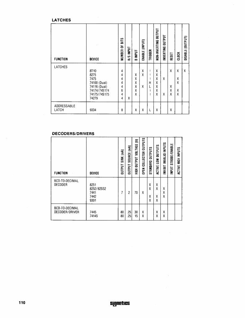
LATCHES
I-:::::) Q..
l- I-:::::) i=' en Q 0 Q.. :::::)
l- i=' t:;I I- Q.. iii :::::) z: :::::) l-Ll..
Q.. ~ Q =:l Q ...... ~ a:: t::l e. ci::
:::::) L.L.I z: Q.. I- L.L.I a:: :> ~
L.L.I L.L.I :::::) L.L.I :!: ..J CD :!: ...... t::l a:: I- ::..::: CD ::E
Q.. CD t::l :Z: u.J L.L.I t.:) c::c en :!: < = :> en Q en FUNCtiON DEVICE
:::::) ......... z: Q :!: L.L.I ..J
C z: a:: CI L.L.I I- z: a:: t.:)
LATCHES 8T10 4 X 1 X X X X 8275 4 X X 1 X 7475 4 X 1 X X X 74100 (Dual) 4 X H X X 74116 (Dual) 4 X X L X X 74174174S174 6 X 1 X X X 74175174S175 4 X 1 X X X X 74279 4 X
ADDRESSABLE LATCH 9334 8 X X L X X
DECODERS/DRIVERS
~ en I-'-:::::) en
L.L.I Q.. L.L.I
<' t::l I- en I- ..J
< :::::) en I- :::::) CD en §. I- Q I- :::::) Q.. < I-<' ..J a:: :::::) Q.. :!: z: :::::)
§. L.L.I Q Q.. I- L.L.I Q.. t.:) :> Q I- :::::) CI ......... :!: ::..::: a:: I- :::::) Q :::J L.L.I
l- t.:) CD z: :::::) :::::) L.L.I Q
== < Q ::J::
Ci5 Q
Q.. ..J C :> a:: t::l en ......J Q :!: ;: I- a:: ..J l-
I- I- ::::i:) Q < en
:::::) :::::) Q t.:)
CI L.L.I I- L.L.I Q.. Q.. z: :z: :> iii I- :> l- I- :z: L.L.I < ~ :c :::::) ~ t::l a..
FUNCTION DEVICE :::::) :::::) :c Q.. l- t.:)
:!: ~ t.:)
Q Q Q en < <
BCD-TO-DECIMAL DECODER 8251 X X
8252/82S52 X X X 7441 7 2 70 X X 7442 X X X 9301 X X
BCD-TO-DECIMAL DECODER/DRIVER 7445 80 .25 30 X X X
74145 80 .25 15 X X X
110 GmDOliCG
INTRODUCTION Recent trends in system design are focusing on significantly lower costs and greater reliability while simultaneously maintaining or improving system performance. Consequently, second generation as well as new system designs demand alternatives to conventional logic realizations which substantially reduce the system manufacturing costs. Signetics' System Logic Family provides this alternative by employing state-ofthe-art technology to produce Large-ScaleIntegrated, system oriented building blocks. By replacing a relatively large number of conventional logic circuits with a few System Logic components, system costs are reduced in proportion to system printed circuit board area, total number of circuits and power requirements. Moreover, system reliability is increased in direct proportion to the decrease in the number of integrated circuits within the system.
SYSTEM LOGIC FAMILY Signetics' System Logic offers the designer a dual technology logic family to achieve cost objectives. First, where speed is a primary objective, low power Schottky TTL technology is employed to yield devices which feature high speed, low power, and medium density. Therefore, significant reduction in the number of high speed logic components is possible without any sacrifice in performance. The distinct advantages of low power Schottky TTL give it one of the best technologies for high performance LSI design. The particular features of LS are:
• Comparable propagation delay to standard TTL7-10ns/gate average
• Low power dissipation-2mW per gate typical at 50% duty cycle
• Low speed power product-19pj typical • 45MHz typical maximum J-K flip-flop clock
frequency • High fan-outcapability-22 unit load-LS input
current requirement is % that of standard TTL (0.36mA/input). Outputs are capable of sinking 8mA.
• High logic density-70 gates/mm2 of silicon • Higher system reliability due to reduced power
density.
Secondly, while lower power Schottky offers increased density at high speeds, substantial component reduction is achieved with devices employing Integrated Injection Logic (l2L). The very high density and low power of 12L makes it extremely attractive for use in realizing relatively large system building blocks. System level functions may each be accomplished at 10MHz speeds by a single 12L integrated circuit. 12L features are:
• Speed-comparable to T2L (10-20ns propagation delay)
• Power-1-2 orders lower than any technology power down mode
• Density-40% smaller than PMOScomparable to NMOS
• Interface-capability of mixing T2L, ECL circuits on the same chip.
The System Logic series of products are specially designed to aid system logic designers in the design of high performance, cost effective systems with a minimal number of parts. This is achieved through a line of standard products which are designed with the following objectives:
• Large Scale Building Blocks-devices are partitioned by function with high-level complexity and sophistication. These one chip building blocks are equivalent to 400 to 1500 elementary logic gates.
• Highest Performance Possible-devices in each category are optimized in performance according to their requirements. Devices requiring highest speed are designed using low power Schottky TTL and devices requiring medium speed are designed using 12L to minimize device power dissipation and maximize logic density.
• Off-the-shelf items-system logic devices are designed to allow general purpose usage. Devices in this series can be used as stand-alone items to enhance performance on a certain system design or to utilize several components within the family to design a minimal cost system with minimum number of components, such as in microprocessor based systems.
SIGNETICS CAPABILITIES Signetics is a leader in the development of bipolar LSI logic circuits using both LS and 12L technologies. Our capabilities are demonstrated by an 8-bit fixed Instruction Microprocessor that Signetics is presently manufacturing with low power Schottky technology.
This circuit, the 8X300 Interpreter, contains the equivalent of 700 logic gates on a 250X250 mil chip. This capability is being used to develop the System Logic Family and _produce the substantial cost reduction offered by LSI without paying a penalty in performance.
Signetics is a forerunner in 12L technology. Signetics has been researching 12L as a standard product technology for over three years. Presently, Signetics possesses one of the fastest 12L processes in the industry. Recognizing the vast potential of 12L technology, Signetics is heavily committed to develop this high-speed line of LSI products using this technology. Signetics' 12L process is basically the same process as its low power Schottky process that utilizes a thin expitaxial layer for speed improvement. Since this process is a highly reliable standard process in Signetics, the confidence
USING STANDARD LS PROCESS
level of producing such LSI circuits is extremely high. In addition to its own development activities, Signetics has access to N.V. Philips' vast development resources for continued development and enhancement of its present capabilities. This massive investment will result in continued improvement in speed/power performance of 12L products.
Table 1 shows expected trends in 12L speed/power curves during the next five years. Clearly 12L will playa major role in the innovation of faster and possibly more complex System Logic functions in the support of a continued exploitation of LSI circuitry in systems design.
ADVANTAGES The advantages of using LSI in system design are manyfold. First, note that the cost of an LSI chip is no more than the sum cost of the circuits it replaces, consequently there is a direct saving in manufacturing costs as a result of a net reduction in the number of parts. Moreover an LSI system offers economic advantages over an SSI or MSI approach besides lowering direct manufacturing costs. Some important considerations are:
• Power supply costs are reduced because logic cells internal to the device require less drive capability and consequently consume less power.
• Field repair costs are reduced because reliability is higher with an LSI implementation. This higher reliability is achieved because IC failure rates are largely proportional to number of devices rather than device complexity.
• Another factor to be considered is that the development cost of printed circuit boards will decrease because of smaller number of ICs and that to some extent, this reduction offsets the cost of layout on the LSI devices.
• Applications requiring medium speed performance are often forced to use lower density, high speed semiconductor devices due to lack of availability of medium speed LSI devices. 12L has changed this picture significantly. With the capability of controlling the amount of device injection curre~t into an LSI circuit, the device can be controlled to operate at the desired speed and power for that particular application; thus, power consumption is minimized.
Average Propagation Delay 1 0-20ns at 200tlA/Gate Injection Cu rrent Density (Dual Layer Metal) Shift Register etc. 320 gates/mm2
Random Logic -150 gates/mm2
Single Inverter -1.5 mil2 Chip Complexity 2000 gates at maximum speed (Random Logic)
4000 gates at maximum speed (Regular Arrays) Speed-Power 3pj @ maximum speed
0.35pj @ < 1 MHz
Table 1 SIGNETICS 12L CAPABILITY
Si!lDOliCS 111
SYSTEM LOGIC PRODUCT FAMILY
• Microprocessors • Peripheral I/O • Miscellaneous
the System logic series. Products with part numbers assigned are either released or under development. Devices with no part numbers assigned are on the product plan. New products will be added to the family tree at regular intervals. A brief description of the System logic devices is given in the pages that follow.
Signetics' System logic series of products can be categorized into five major groups according to their function. Grouping is as follows:
• Communications • Memory
IN PRODUCTION
Circuits within each group are interrelated in function, thus insuring compatibility both in electrical characteristics and in technology.
Figure 1 illustrates the type of products in
SYSTEM LOGIC PRODUCT STATUS
New Products
PLANNED 8X01-Cyclic Redundancy Check
Generator/Checker 8X05-Direct Memory Access Control Unit
-1200 Gates at 10MHz
112
-150 Gates at 10MHz (Typical) -1 2 l Technology
8X02-Control Store Sequencer -300 Gates -lS Technology
8X08-Frequency Synthesizer
MISCELLANEOUS
FREQUENCY SYNTHESIZER 8X08
PERIPHERAL/I/O
(8X05) DMACONTROL
MULTIPLIER
MULTI·PORT MEMORY CONTROL
MULTI-INPUT PIPELINED I/O PORT
PERIPHERAL INTERFACE UNIT
-12l Technology
8X06-64X8 FIFO -3000 Gates at 10MHz -1 2 l Technology
8X07-64X9 FIFO -3000 Gates at 10MHz -1 2 l Technology
8X -16X8 LIFO -600 Fates at 10MHz -1 2 l Technology
8X -Multiplier -1 2 l Technology
8X -Dual Port Register File -lS Technology
8X -Pipe Lined I/O Port -LS Technology
8X -Peripheral Interface Unit -1 2 l Technology
SIGNETICS SYSTEM LOGIC FAMILY
SYSTEM LOGIC FAMILY
I'PROCESSOR/SUPPORT
8X300 8·BIT !,CONTROLLER
3001
MEMORY
8X06/8X07 64X8/64X9 FIFO
MICROPROGRAM CONTROL UNIT
3002 2·BIT CENTRAL PROC. ELEMENT
8X02 (CONTROL STORE SEQUENCER)
DUAL PORT REGISTER FILE
Figure 1
S(gOOliCS
COMMUNICATIONS
8X01 CRC
OBJECTIVE SPECIFICATION
DESCRIPTION The CRC Generator/Checker circuit is used to provide an error detection capability for serial digital data handling system. The serial data stream is divided by a selected polynomial and the division remainder is transmitted at the end of the data stream, as a Cyclic Redundancy check character (CRCC). When the data is received, the same calculation is performed. If the received message is error-free, the calculated remainder should satiSfy a predetermined pattern. In most cases, the remainder is zero except in the case where Synchronous Data Link Control type protocols are used whereby the correct remainder is checked for 1111000010111000 (xO - x 15).
8 polynomials are provided and can be se-
FEATURES • 12L technology • TTL inputs/outputs • 10MHz (max) data rate • Total power dissipation = 175mw (max) • Vcc = 5.0V • VJJ = 1.0V • Separate preset and reset controls • SOLC specified pattern match • Automatic right justification
TYPICAL APPLICATIONS • Floppy and other disc systems • Digital cassette and cartridge systems • Data communication systems
8X01-A,F
PIN CONFIGURATION
A,F PACKAGE
ep Vee
ER
so a
MR D
eWE
GND
lected via a 3-bit control bus. Popular RECOMMENDED OPERATING CONDITIONS polynomials such as CRC-16 and CCITT are implemented. Polynomials can be programmed to start with either all zeros or all ones.
Automatic right justification for polynomials of degree less than 16 is provided.
FUNCTIONAL DESCRIPTION The CRC Generator/Checker circuit provides a means of detecting errors in a serial data communications environment. A binary message can be interpreted as a binary polynomial H(x). This polynomial can be divided by a generator polynomial P(x) such that H(x) = P(x) Q(x) + R(x) whereby Q(x) is the quotient and P(x) is the remainder. During transmission, the remainder is appended to the end of the message as check bits. For a given message, a unique remainder is generated. Hardware implementation of division is simply a feedback shift register with Exclusive-OR gating. Subtraction and addition in modulo 2 is implemented by the Exclusive-OR function. The number of shift register stages is equal to the degree of the divisor polynomial.
Table 1 shows the polynomials implemented in the CRC circuit. Each polynomial can be selected via the 3-bit polynomial control inputs So, S1 and S2. To generate the check bits, the data stream is entered via the Data (D) input, using the high to low transition of the Clock (CP) input. This data is gated with the most significant output (Q) of the register, and controls the exclusive OR gates. The Check Word Enable (CWE) must be held high while the data is being entered. After the last data bit is entered, the CWE is brought low and the check bits are shifted out of the register and appended to the data bits using external gating.
PARAMETER MIN
VCC Supply voltage 4.75 IJJ Supply current 40
To check an incoming message for errors, both the data and check bits are entered through the D input with the CWE input held high. The 8X01 is not in the data path, but only monitors the message. The Error output becomes valid after the last check bit has been entered into the 8X01 by a high to low transition of CP. If no detectable errors have occurred during the data transmission, the resultant internal register bits are all low and the Error output (ER) is low. If a detectable error has occurred, ER is high. ER remains valid until the next high to low transition of CP or until the device has been preset or reset. PME must be high if ER output is used to reflect all zero result.
For data communications using the Synchronous Data Link Control protocol (SDLC), the 8X01 is first preset to all ones before any accumulation is done. This applies to both transmitter and receiver.
A special pattern of 1111000010111000 (xO
- X 15) is used in place of all zeros during receiving for valid message check. PME is incorporated to select this option. If PME is low during the last bit time of the message, ER output is low if result matches this special pattern. When ER is high, error has occurred.
A high level on the Master Reset (MR) input asynchronously clears the register. A low level on the Preset (P) input asynchronously sets the entire register if the control code inputs specify a 16-bit polynomial; in the
!ii!lDotiC!i
LIMITS
TVP MAX UNIT
5.0 5.25 V 100 mA
case of the 12 or 8-bit check polynomials only the most significant 12 or 8 register bits are set and the remaining bits are cleared.
PIN DESIGNATIONS
PIN NO. FUNCTION
SO, S1, S2 Polynominal Select inputs
0 Data input
CP Clock (operates on high to low transition) input
CWE Check Word Enable
P Preset (active low) input
MR Master Reset (active high) input
Q Data output
ER Error (active high) output
PME Pattern match enable (active low)
113
OBJECTIVE SPECIFICATION
TRUTH TABLE
SELECT CODE
S2 S1 So
L L L
L L H
L H L
L H H
H L L
H L H
H H L
H H H
LOGIC DIAGRAM
DATA IN
CP
MASTER RESET
POLYNOMIAL
X16+X15+X2+ 1
X16+X14+X+ 1
X16+X15+X13+X7+X4+X2+X1+1
X12+X11+X3+X2+X+ 1
X8+X7+X5+X4+X+1
X8+1
X16+X12+X5+ 1
X16+X11+X4+ 1
POLYNOMIAL SELECT LOGIC
REMARKS
CRC-16
CRC-16 REVERSE
CRC-12
LRC-8
CRC-CCITT
CRC-CCITT REVERSE
DATA OUT
DC CHARACTERISTICS OVER OPERATING TEMPERATURE RANGE (Unless Otherwise Noted)
LIMITS
PARAMETER TEST CONDITIONS MIN TYP MAX UNIT
V,H Input high voltage 2.0 V
V,L Input low voltage 0.8 V
V Ie Input clamp diode voltage Vee = MIN, liN = 18mA -1.5 V
VOH Output high voltage Vee = MIN, 10H = 400p,A 2.7 V
VOL Output low voltage Vee = MIN, 10L = 8mA 0.5 V
"H Max. input current Vee = MAX 0.1 rnA
"H Input high current vee = MAX, V IN = 2.7V 20 p,A
I,L Input low current vee = MAX, V,N = OAV -0.36 rnA
lOS Output short circuit current vee = MAX, VOUT = OV -10 -42 mA
IJJ Injection current Vee = MAX, Inputs open 60 100 mA
I ee Supply current Vee = MAX, inputs open 10 18 mA
114 S!!IDOliCS
8X01-A,F
12L INJECTOR CURRENT SOURCE
VCC - V JJ (5.0 - 0.8) V RJJ
Ijj 60mA
= 4.20V = 700n 60mA
TEST CIRCUIT
INPUT IOUTPUT CIRCUITS
FROM
12 l
TTL INPUTS
INPUT STRUCTURE
OUTPUT STRUCTURE
TTL OUTPUTS
NOTE: ALL RESISTORS VALUES ARE TYPICAL AND IN OHMS.
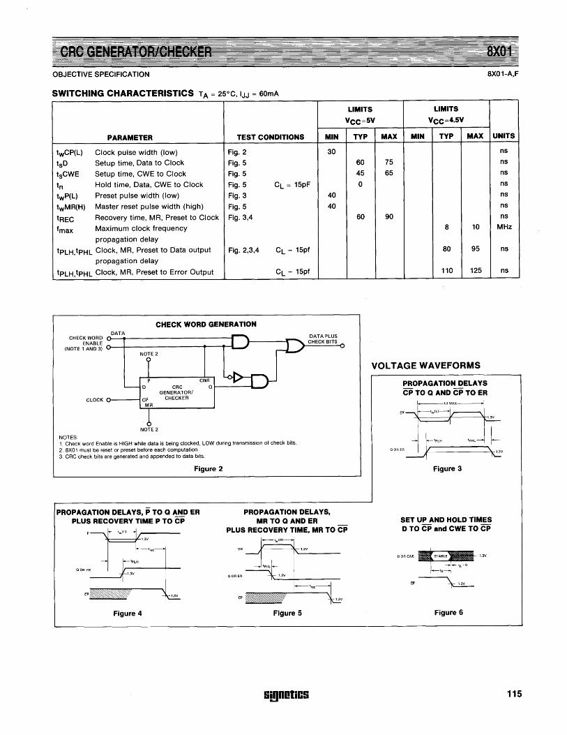
OBJECTIVE SPECIFICATION
SWITCHING CHARACTERISTICS TA = 25°C, IJJ = 60mA
PARAMETER TEST CONDITIONS
twCP(L) Clock pulse width (low) Fig. 2
tsD Setup time, Data to Clock Fig. 5
tsCWE Setup time, CWE to Clock Fig. 5
tn Hold time, Data, CWE to Clock Fig. 5
twP(L) Preset pulse width (low) Fig. 3
twMR(H) Master reset pulse width (high) Fig. 5
tREC Recovery time, MR, Preset to Clock Fig. 3,4
fmax Maximum clock frequency
propagation delay
tPLH,tPHL Clock, MR, Preset to Data output Fig. 2,3,4
propagation delay
tpLH,tpHL Clock, MR, Preset to Error Output
CHECK WORD GENERATION DATA
CHECK WORD 0-......... ------------1 (NOTE 1E~~gL3~ o-~~-------__._-__._-L~
NOTES:
NOTE 2
P D
CLOCK 0----1 CP MR
NOTE 2
CWE CRC Q I-------i'--J
GENERATOR/ CHECKER
CL = 15pF
CL = 15pf
CL = 15pf
1. Check word Enable is HIGH while data is being clocked. LOW during transmission of check bits. 2. 8XO 1 must be reset or preset before each computation 3. CRC check bits are generated and appended to data bits.
Figure 2
MIN
30
40
40
PROPAGATION DELAYS, P TO Q AND ER PLUS RECOVERY TIME P TO CP
PROPAGATION DELAYS, MRTO Q AND ER
LIMITS LIMITS
VCC=5V VCC=4.5V
TYP MAX MIN TYP MAX
60 75
45 65
0
60 90 8 10
80 95
110 125
VOLTAGE WAVEFORMS
PROPAGATION DELAYS CP TO Q AND CP TO ER
Figure 3
8X01-A,F
UNITS
ns
ns
ns
ns
ns
ns
ns
MHz
ns
ns
PLUS RECOVERY TIME, MR TO CP SET UP AND HOLD TIMES D TO CP and CWE TO CP
DOR eWE
Figure 4 Figure 5 Figure 6
Si!lDotiCS 115
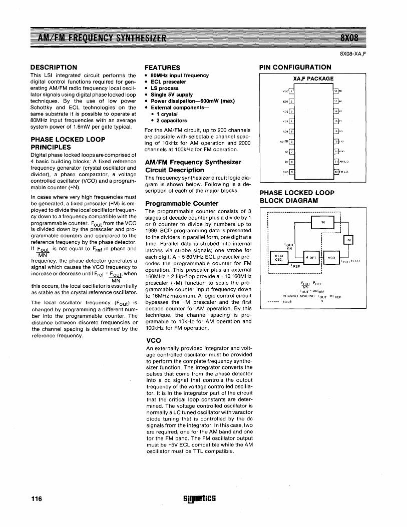
AM FM FREQIIENCY SYNtHESllER
DESCRIPTION This lSI integrated circuit performs the digital control functions required for generating AM/FM radio frequency local oscillator signals using digital phase locked loop techniques. By the use of low power Schottky and Eel technologies on the Same substrate it is possible to operate at 80M Hz input frequencies with an average system power of 1.6mW per gate typical.
PHASE LOCKED LOOP PRINCIPLES Digital phase lOcked loops are comprised of 4 basic building blocks: A fixed reference frequency generator (crystal oscillator and divider), a phase comparator, a voltage controlled oscillator (VCO) and a programmable counter (+N).
In cases where very high frequencies must be generated, a fixed prescaler (+M) is employed to divide the local oscillatorfrequency down to a frequency compatible with the programmable counter. Fout from the VCO is divided down by the prescaler and programmable counters and compared to the reference frequency by the phase detector. If Fout is not equal to Fref in phase and
MN frequency, the phase detector generates a signal which causes the VCO frequency to increase or decrease until Fref = F out, when
MN this occurs, the local oscillator is essentially as stable as the crystal reference oscillator.
The local oscillator frequency (Fout) is changed by programming a different number into the programmable counter. The distance between discrete frequencies or the channel spacing is determined by the reference frequency.
116
FEATURES • 80MHz input frequency • ECl prescaler • lS process • Single 5V supply • Power dissipation-600mW (max) • External components-
• 1 crystal • 2 capacitors
For the AM/FM circuit, up to 200 channels are possible with selectable channel spaci ng of 10kHz for AM operation and 2000 channels at 100kHz for FM operation.
AM/FM Frequency Synthesizer Circuit Description The frequency synthesizer circuit logic diagram is shown below. Following is a description of each of the major blocks.
Programmable Counter The programmable counter conSists of 3 stages of decade counter plu~ a divide by 1 or 0 counter to divide by numbers up to 1999. BCD programming data is presented to the dividers in parallel form, one digit at a time. Parallel data is strobed into internal latches via strobe signals; one strobe for each digit. A + 5 80MHz ECl prescaler precedes the programmable counter for FM operation. This prescaler plus an external 160MHz + 2 flip-flop provide a + 10 160MHz prescaler (+M) function to scale the programmable counter input frequency down to 16MHz maximum. A logic control circuit bypasses the +M prescaler and the first decade counter for AM operation. By this technique, the channel spacing is programable to 10kHz for AM operation and 100kHz for FM operation.
VCO An externally provided integrator and voltage controlled osCillator must be provided to perform the complete frequency synthesizer function. The integrator converts the pulses that come from the phase detector into a dc signal that controls the output frequency of the voltage controlled oscillator. It is in the integrator part of the circuit that the critical loop constants are determined. The voltage controlled oscillator is normally a lC tuned oscillator with varactor diode tuning that is controlled by the dc signals from the integrator. In this case, two are required, one for the AM band and one for the FM band. The FM oscillator output must be +5V ECl compatible while the AM oscillator must be TTL compatible.
Si!lDotiCS
PIN CONFIGURATION
XA,F PACKAGE
PHASE LOCKED LOOP BLOCK DIAGRAM
IX"8
8X08-XA,F
r-- - - - - - - - - - - - - - - - - - - - - -- - - - - - - - - - - - - --1
FOUl FREF MN
FOUl = MNREF
CHANNEL SPACING FOUl MFREF
8X08 -N-
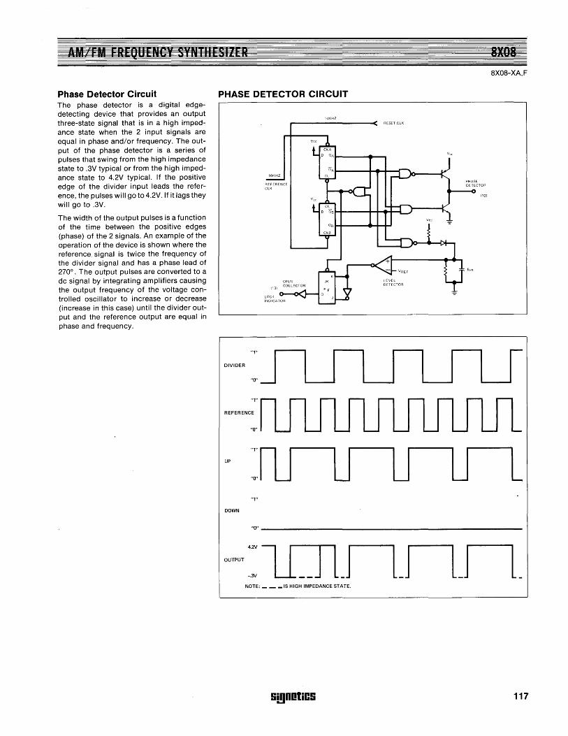
#\11 FM FREQUENCV SYNTIIESIIER 8108
Phase Detector Circuit The phase detector is a digital edgedetecting device that provides an output three-state signal that is in a high impedance state when the 2 input signals are equal in phase and/or frequency. The output of the phase detector is a series of pulses that swing from the high impedance state to .3V typical or from the high impedance state to 4.2V typical. If the positive edge of the divider input leads the reference, the pulses will go to 4.2V. If it lags they will go to .3V.
The width of the output pulses is a function of the time between the positive edges (phase) of the 2 signals. An example of the operation of the device is shown where the reference signal is twice the frequency of the divider signal and has a phase lead of 2700
• The output pulses are converted to a dc signal by integrating amplifiers causing the output frequency of the voltage controlled oscillator to increase or decrease (increase in this case) until the divider output and the reference output are equal in phase and frequency.
8X08-XA,F
PHASE DETECTOR CIRCUIT
1121
1131
LOCK
DIVIDER ::J I I I I I I I I "1"
REFERENCE
"0"
UP "'T1J "0" u u u L "1"
DOWN
"0" _______________ -------------
NOTE: ___ IS HIGH IMPEDANCE STATE.
S!!)DotiCS 117
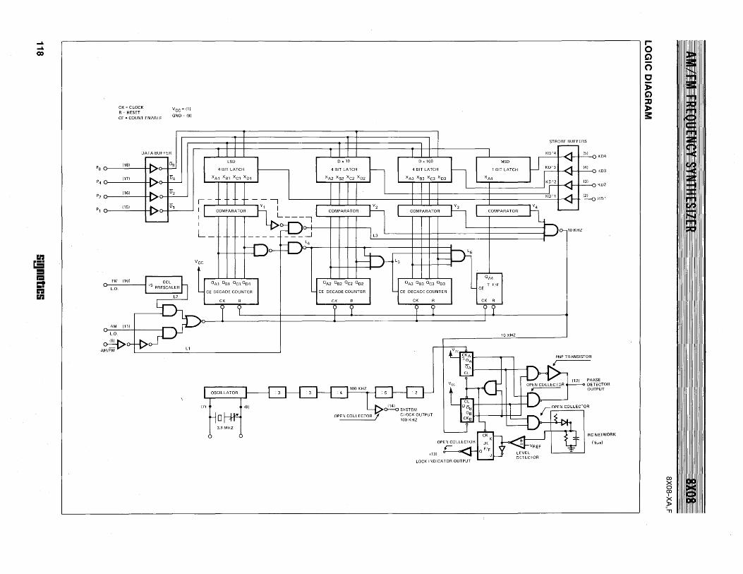
Ps
P4
P2
P1
FM
L.O.
L.O.
CK = CLOCK R = RESET CE = COUNT ENABLE
DATA BUFFER
11S1
1171
1161
1151
~ AM/FM
VCC = 111
GND = 191
10 XHZ
KD4
KD3
KD2
KDl
PHASE DETECTOR OUTPUT
RC NETWORK
(5.51
ex> X o ex> X ]> 11
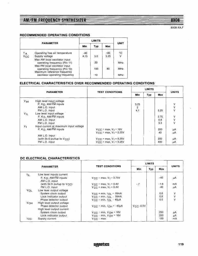
AM EM FRFQIIFNlZf SfNTHESI1FR 8X08 axoa-XA,F
RECOMMENDED OPERATING CONDITIONS
LIMITS PARAMETER UNIT
Min Typ Max
TA Operating free air temperature -40 +a5 °e Vee Supply voltage 4.75 5.0 5.25 V
Max AM local oscillator input operating frequency (Pin 11) 20 MHz
Max FM local oscillator input operating frequency (Pin 10) 100 ao MHz
Maximum reference frequency oscillator operating frequency 10 MHz
ELECTRICAL CHARACTERISTICS OVER RECOMMENDED OPERATING CONDITIONS
LIMITS PARAMETER TEST CONDITIONS UNITS
Min Typ Max
VIH High level input voltage P, K 0, AM/FM inputs 5.25 V AM L.O. input 2 V FM L.O. input 4.1 5.25 V
VIL Low level input voltage P, K 0, AM/FM inputs 3.75 V AM L.O. input o.a V FM L.O. input 3.3 V
VI Input current at maximum input voltage P, K 0, AM/FM inputs Vee = max, V I = 16V 200 J.1A
Vee = max, VI = 5.25V 40 J.1A AM L.O. input (with 5k n pullup to Vec) Vee = max, VI = 5.25V 200 J.1A FM L.O. input Vee = max, VI = 5.25V 400 j.1A
DC ELECTRICAL CHARACTERISTICS
LIMITS PARAMETER TEST CONDITIONS UNITS
Min Typ Max
IlL Low level inputs current P, K 0, AM/FM inputs Vee = max, VI = 3.75V -40 j.1A AM L.O. input (with 5k n pullup to Vee) Vee = max, VI = OAV -.7 -1.6 mA FM L.O. input Vee = max, VI = OAV -40 j.1A
VOL Low level output voltage System clock output Vee = min, IOL = 16mA o.a V Lock indicator output Vee = min, IOL = 16mA o.a V Phase detector output Vee = min, IOL = 40J.1A 0.5 V
VOH High level output voltage Phase detector output Vee = min, IOH = -40j.1A Vee-O.5V
High level output current System clock output Vee = min, VOH = 16V 250 j.1A Lock indicator output Vee = min, VOH = 16V 250 j.1A
lee Supply current Vee = max 130 mA
!ii!lDotiC!i 119
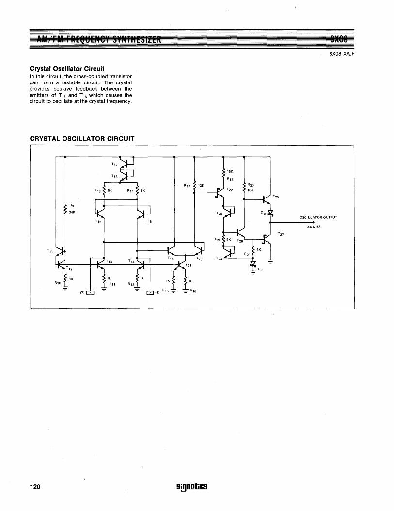
ii" I M I'EQIII NOI SIN I HESIZER
Crystal Oscillator Circuit In this circuit, the cross-coupled transistor pair form a bistable circuit. The crystal provides positive feedback between the emitters of T15 and T 16 which causes the circuit to oscillate at the crystal frequency.
CRYSTAL OSCILLATOR CIRCUIT
120
Rg
34K
8"08 8X08-XA,F
R17 13K
OSCILLATOR OUTPUT
3.6 MHZ
!i!!lDotiC!i
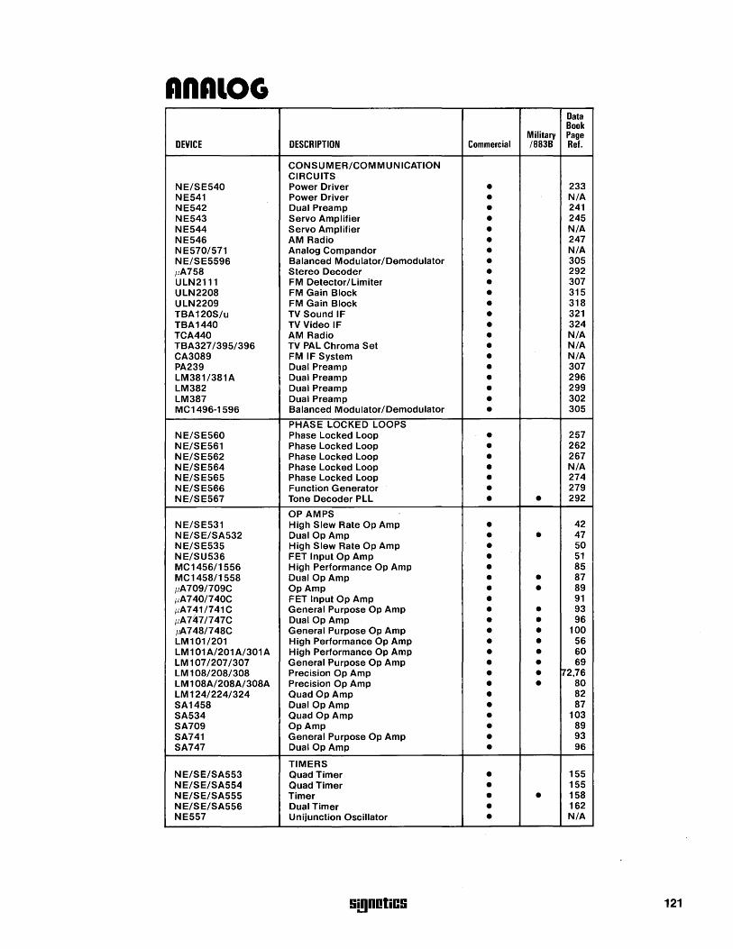
AnAlOG Data Book
Military Page DEVICE DESCRIPTION Commercial /883B Ref.
CONSUMER/COMMUNICATION CIRCUITS
NE/SE540 Power Driver • 233 NE541 Power Driver • N/A NE542 Dual Preamp • 241 NE543 Servo Amplifier • 245 NE544 Servo Amplifier • N/A NE546 AM Radio • 247 NE570/571 Analog Compandor • N/A NE/SE5596 Balanced Modulator/Demodulator • 305 flA758 Stereo Decoder • 292 ULN2111 FM Detector/Limiter • 307 ULN2208 FM Gain Block • 315 ULN2209 FM Gain Block • 318 TBA120S/u TV Sound IF • 321 TBA1440 TV Video IF • 324 TCA440 AM Radio • N/A TBA327/395/396 TV PAL Chroma Set • N/A CA3089 FM IF System • N/A PA239 Dual Preamp • 307 LM381/381A Dual Preamp • 296 LM382 Dual Preamp • 299 LM387 Dual Preamp • 302 MC1496-1596 Balanced Modulator/Demodulator • 305
PHASE LOCKED LOOPS NE/SE560 Phase Locked Loop • 257 NE/SE561 Phase Locked Loop • 262 NE/SE562 Phase Locked Loop • 267 NE/SE564 Phase Locked Loop • N/A NE/SE565 Phase Locked Loop • 274 NE/SE566 Function Generator • 279 NE/SE567 Tone Decoder PLL • • 292
OP AMPS NE/SE531 High Slew Rate Op Amp • 42 NE/SE/SA532 Dual Op Amp • • 47 NE/SE535 High Slew Rate Op Amp • 50 NE/SU536 FET Input Op Amp • 51 MC1456/1556 High Performance Op Amp • 85 MC1458/1558 Dual Op Amp • • 87 flA 709/709C OpAmp • • 89 flA74O/740C FET Input Op Amp • 91 flA741 /741C General Purpose Op Amp • • 93 flA747/747C Dual Op Amp • • 96 ~748/748C General Purpose Op Amp • • 100 LM101/201 High Performance Op Amp • • 56 LM 101 A/201 A/301 A High Performance Op Amp • • 60 LM 1 07/207/307 General Purpose Op Amp • • 69 LM 1 08/208/308 Precision Op Amp • • 172,76 LM108A/208A/308A Precision Op Amp • • 80 LM 124/224/324 Quad OpAmp • 82 SA1458 Dual Op Amp • 87 SA534 Quad Op Amp • 103 SA709 OpAmp • 89 SA741 General Purpose Op Amp • 93 SA747 Dual Op Amp • 96
TIMERS NE/SE/SA553 Quad Timer • 155 NE/SE/SA554 Quad Timer • 155 NE/SE/SA555 Timer • • 158 NE/SE/SA556 Dual Timer • 162 NE557 Unijunction Oscillator • N/A
!ii!)DotiC!i 121
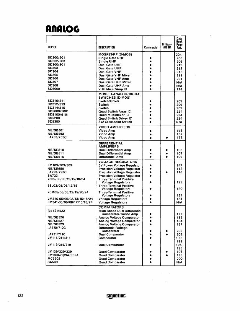
AnAlOG Data Book
Military Page DEVICE DESCRIPTION Commercial /883B Ref.
MOSFET-RF (D-MOS) 204, SD200/201 Single Gate UHF • 206 SD202/203 Single UHF • 206 SD300/301 Dual Gate UHF • 212 SD303 Dual Gate UHF • 212 SD304 Dual Gate VHF • 212 SD305 Dual Gate VHF Mixer • 218 SD306 Dual Gate VHF Amp • 221 SD307 Dual Gate UHF Mixer • N/A SD308 Dual Gate UHF Amp • N/A SD6000 VHF Mixer/Amp IC • 228
MOSFET-ANALOG/DIGITAL SWITCH ES (D-MOS)
SD210/211 Switch/Driver • 209 SD212/213 Switch • 209 SD214/215 Switch • 209 SD5000/5001 Quad Switch Array IC • 224 SD5100/5101 Quad Multiplexer IC • 224 S05200 Quad Switch Driver IC • 224 SD5300 8x2 Crosspoint Switch • N/A
VIDEO AMPLIFIERS NE/SE501 Video Amp • 166 NE/SE592 Video Amp • 167 /-lA733/733C Video Amp • • 172
01 FFE R ENTIAL AMPLIFIERS
NE/SE510 Dual Differential Amp • • 106 NE/SE511 Dual Differential Amp • • 107 NE/SE515 Differential Amp • • 109
VOLTAGE REGULATORS LM 1 09/209/309 5V Power Voltage Regulator • 147 NE/SE550 Precision Voltage Regulator • 112 /-lA723/723C Precision Voltage Regulator • • 116 SA723 Precision Voltage Regulator • 7805/06/08/12/15/18/24 Three Terminal Positive
Voltage Regulators • 122 78L02/05/06/12/15 Three-Terminal Positive
Voltage Regulators • 130 78M05/06/08/12/15/20/24 Three-Terminal Positive
Voltage Regulators • 139 LM 340-05/06/08/12/15/18/24 Voltage Regulators • 151 LM341-05/06/08/12/15/18/24 Voltage Regulators • N/A
COMPARATORS NE521/522 High Speed Dual Differential
Comparator/Sense Amp • 177 NE/SE526 Analog Voltage Comparator • 183 NE/SE527 Analog Voltage Comparator • 184 NE/SE529 Analog Voltage Comparator • 187 /-lA71 0!71 OC Differential Voltage
Comparator • • 202 /-lA711/711C Dual Comparator • • 203 LM111/211/311 Comparator • 190,
192 LM119/219/319 Dual Comparator • 194,
195 LM139/239/339 Quad Comparator • • 197 LM139A/2\39A/339A Quad Comparator • • 198 MC3302 Quad Comparator • 200 SA539 Quad Comparator • N/A
122 Si!lDOliCS

CIIAPTIR4 APPliCATions
!i!!lDotiC!i 123

124 !i!!lDOliC!i
INTRODUCTION The ability of the semiconductor industry to manufacture complete general purpose processors on single chips represents a significant technological advance which should prove to be of great benefit to digital systems manufac~urers. In terms of chip size and density of transistors, the processors are simply extensions of the continually evolving MaS technology. But in terms of function provided, a significant threshold has been crossed.
By allowing designers to convert from hardware logic to programmed logic, the integrated processor provides several important advantages.
1. Logic functions may be implemented in memory bits instead of logic gates. The user then has greater access to the advantages of memory circuits. Memories use patterned circuitry and thus provide greater density and therefore greater economy.
2. Random logic implementations of complex functions are highly specialized and cannot be used in other applications. They are not often used in large volume. Programmed logic, on the other hand, relies on general purpose processor and memory circuits that are used in
many applications. Thus, economies of volume are available for both the user and the manufacturer.
3. Because the functional specialization resides in the user's program rather than the hardware logic, changes, corrections and additions can be much easier to make and can be accomplished in a much shorter time.
4. With the programmed logic approach it is often possible to add new features and create new products simply by writing new programs.
5. The design cycle of a system using programmed logic can be significantly shorter than a similar system that attempts to use custom random logic. The debugging cycle is also greatly compressed.
A general purpose processor designed to implement programmed logic has many characteristics that allow it to do conventional computer operations as Well. Many applications will specialize in programmed logic or in data processing, but some will take advantage of both areas. In a line printer application, for example, a processor can act primarily as a controller handling the housekeeping duties, control sequencing and data interfacing for the printer. It also might buffer the data or do some code conversions, but that is not its primary duty. On the other hand, in a text
!ii!lDotiC!i
editing intelligent terminal, the processor is mainly concerned with data manipulation since it handles code translations, display paging, insertions, deletions, line justification, hyphenation, etc.
A pOint-of-sale type of terminal represents an application that combines both control and data processing activities for the processor. Coordinating the activities of the various devices and displays that make up the terminal is an important part of the job,
as are the calculations that are essential to the operation of the machine.
Because of the diversity of application areas, a single microprocessor type cannot effectively service all applications. Signetics offers a variety of microprocessor families, each of which has specific benefits in the various application areas.
This chapter contains hardware and software application memos for the 8X300, 3000 families. Additional application memos are in preparation. The services of a field applications engineer or the factory microprocessor applications staff are also available.
125
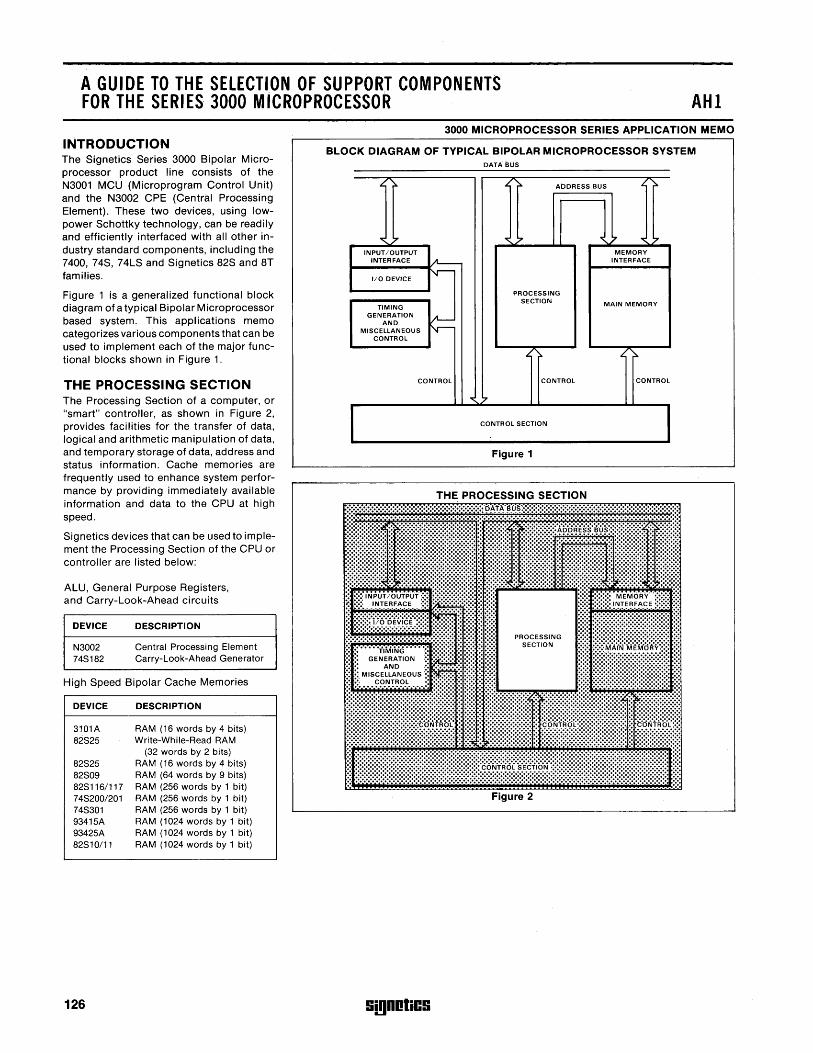
A GUIDE TO THE SELECTION OF SUPPORT COMPONENTS FOR THE SERIES 3000 MICROPROCESSOR AHI
INTRODUCTION The Signetics Series 3000 Bipolar Microprocessor product line consists of the N3001 MCU (Microprogram Control Unit) and the N3002 CPE (Central Processing Element). These two devices, using lowpower Schottky technology, can be readily and efficiently interfaced with all other industry standard components, including the 7400, 74S, 74LS and Signetics 82S and 8T families.
Figure 1 is a generalized functional block diagram of a typical Bipolar Microprocessor based system. This applications memo categorizes various components that can be used to implement each of the major functional blocks shown in Figure 1.
THE PROCESSING SECTION The Processing Section of a computer, or "smart" controller, as shown in Figure 2, provides facilities for the transfer of data, logical and arithmetic manipulation of data, and temporary storage of data, address and status information. Cache memories are frequently used to enhance system performance by providing immediately available information and data to the CPU at high speed.
Signetics devices that can be used to implement the Processing Section of the CPU or controller are listed below:
ALU, General Purpose Registers, and Carry-Look-Ahead circuits
DEVICE
N3002 748182
DESCRIPTION
Central Processing Element Carry-look-Ahead Generator
High Speed Bipolar Cache Memories
DEVICE
3101A 82825
82825 82809 828116/117 748200/201 748301 93415A 93425A 82810/11
126
DESCRIPTION
RAM (16 words by 4 bits) Write-While-Read RAM
(32 words by 2 bits) RAM (16 words by 4 bits) RAM (64 words by 9 bits) RAM (256 words by 1 bit) RAM (256 words by 1 bit) RAM (256 words by 1 bit) RAM (1024 words by 1 bit) RAM (1024 words by 1 bit) RAM (1024 words by 1 bit)
3000 MICROPROCESSOR SERIES APPLICATION MEMO
BLOCK DIAGRAM OF TYPICAL BIPOLAR MICROPROCESSOR SYSTEM DATA BUS
L. ~ "" ~ ADDRESS BUS L ~
'0:: '?" '0:: 7 " 7 '" 7 INPUT/OUTPUT MEMORY
INTERFACE ,11-- INTERFACE
1/0 DEVICE v---
PROCESSING SECTION MAIN MEMORY TIMING
GENERATION I'-AND
MISCELLANEOUS v---CONTROL
"" r- L. ~
CONTROL CONTROL CONTROL
'" '7
CONTROL SECTION
Figure 1
THE PROCESSING SECTION
Figure 2
Si!lDotiCS
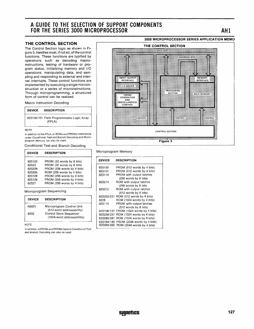
A GUIDE TO THE SELECTION OF SUPPORT COMPONENTS FOR THE SERIES 3000 MICROPROCESSOR AHI
3000 MICROPROCESSOR SERIES APPLICATION MEMO THE CONTROL SECTION The Control Section logic as shown in Figure 3, handles most, if not all, of the control functions. These functions are typified by operations such as decoding macroinstructions, testing of hardware or program status, initializing memory and I/O operations, manipulating data, and sampling and responding to external and internal interrupts. These controi functions are implemented by executing a single microinstruction or a series of microinstructions. Through microprogramming, a structured form of control can be realized.
Macro Instruction Decoding
DEVICE DESCRIPTION
828100/101 Field Programmable Logic Array (FPLA)
NOTE
In addition to the FPLA, all ROMs and PROMs listed below under Conditional Test and Branch Decoding and Microprogram Memory can also be used.
Conditional Test and Branch Decoding
DEVICE
828123 82823 828229 828226 828129 828126 82827
DESCRIPTION
PROM (32 words by 8 bits) PROM (32 words by 8 bits) PROM (256 words by 4 bits) ROM (256 words by 4 bits) PROM (256 words by 4 bits) PROM (256 words by 4 bits) PROM (256 words by 4 bits)
Microprogram Sequencing
DEVICE
N3001
8X02
NOTE
DESCRIPTION
Microprogram Control Unit (512-word addressability)
Control 8tore 8equencer (1024-word addressability)
In addition,all ROMs and PROMs listed in Conditional Test and Branch Decoding can also be used.
CONTROL SECTION
Microprogram Memory
DEVICE DESCRIPTION
828130 PROM (512 words by 4 bits) 828131 PROM (512 words by 4 bits) 828114 PROM with output latches
(256 words by 8 bits) 828214 ROM with output latches
(256 words by 8 bits 828215 ROM with output latches
(512 words by 8 bits) 828230/231 ROM (512 words by 4 bits) 8228 ROM (1024 words by 4 bits) 828115 PROM with output latches
(512 words by 8 bits) 828136/137 PROM (1024 words by 4 bits) 828236/237 ROM (1024 words by 4 bits) 828280/281 ROM (1024 words by 8 bits) 828184/185 PROM (2048 words by 4 bits) 828284/285 ROM (2048 words by 4 bits)
!i!!lDOliC!i
Figure 3
127
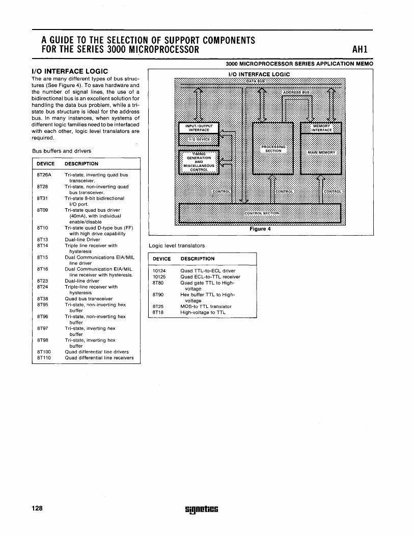
A GUIDE TO THE SELECTION OF SUPPORT COMPONENTS FOR THE SERIES 3000 MICROPROCESSOR AHI
3000 MICROPROCESSOR SERIES APPLICATION MEMO
I/O INTERFACE LOGIC The are many different types of bus structures (See Figure 4). To save hardware and the number of signal lines, the use of a bidirectional bus is an excellent solution for handling the data bus problem, while a tristate bus structure is ideal for the address bus. In many instances, when systems of different logic families need to be interfaced with each other, logic level translators are required.
Bus buffers and drivers
DEVICE DESCRIPTION
8T26A Tri-state, inverting quad bus transceiver.
8T28 Tri-state, non-inverting quad bus transceiver.
8T31 Tri-state 8-bit bidirectional I/O port.
8T09 Tri-state quad bus driver (40mA), with individual enable/disable
8T10 Tri-state quad D-type bus (FF) with high drive capability
8T13 Dual-line Driver 8T14 Triple line receiver with
hysteresis 8T15 Dual Communications EIA/Mll
line driver 8T16 Dual Communication EIA/MIL
line receiver with hysteresis. 8T23 Dual-line driver 8T24 Triple-line receiver with
hysteresis 8T38 Quad bus transceiver 8T95 Tri-state, non-inverting hex
buffer 8T96 Tri-state, non-inverting hex
buffer 8T97 Tri-state, inverting hex
buffer 8T98 Tri-state, inverting hex
buffer 8T100 Quad differential line drivers 8T110 Quad differential line receivers
128
1/0 INTERFACE LOGIC u
~::: ::::: ::::: ::::: :::::::::: :::::::::: :::::::~ iii:: ::::::::::: ::::: :::::: :::::: :::::: ::::: :::::: :::::::: :::::: :::::: ;::: :::::~::::::::::::::::::::::::::::::::::::::::;::::::;:::::::::::::::::::::::::::::::::::::::::::::::::::::f:::::::::::::::::::::::::: I~:m:::::::::::::::::::::::::::::::::::::::::::::::::::~~~~~LSEC:~~::::::::::::::::::::::::::::::::::::::::::::::::;::::::::::: r.~~~~?:::::::::::::::::::::::::::::::::::~~.;;:;:~:~~;;:::~.:.:.:.:.:.:.:.:.:.:::.:.:::.:::::.:::.:;:::::;:::::;::::: ~!:::
Figure 4
Logic level translators
DEVICE
10124 10125 8T80
8T90
8T25 8T18
DESCRIPTION
Quad TTl-to-ECl driver Quad ECl-to-TTL receiver Quad gate TTL to High-
voltage Hex buffer TTL to High
voltage MOS-to TTL translator High-voltage to TTL
Si!lDnliCS
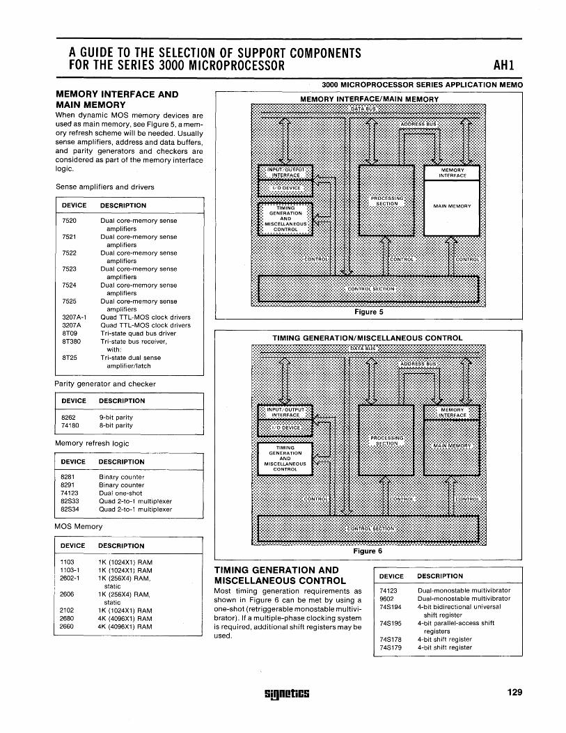
A GUIDE TO THE SELECTION OF SUPPORT COMPONENTS FOR THE SERIES 3000 MICROPROCESSOR AHI
MEMORY INTERFACE AND MAIN MEMORY When dynamic MOS memory devices are used as main memory, see Figure 5, a memory refresh scheme will be needed. Usually sense amplifiers, address and data buffers, and parity generators and checkers are considered as part of the memory interface logic.
Sense amplifiers and drivers
DEVICE DESCRIPTION
7520
7521
7522
7523
7524
7525
3207A-1 3207A 8T09 8T380
8T25
Dual core-memory sense amplifiers
Dual core-memory sense amplifiers
Dual core-memory sense amplifiers
Dual core-memory sense amplifiers
Dual core-memory sense amplifiers
Dual core-memory sense amplifiers
Quad TTL-M08 clock drivers Quad TTL-M08 clock drivers Tri-state quad bus driver Tri-state bus receiver,
with: Tri-state dual sense
amplifier/latch
Parity generator and checker
DEVICE DESCRIPTION
8262 9-bit parity 74180 8-bit parity
Memory refresh logic
DEVICE
8281 8291 74123 82833 82834
DESCRIPTION
Binary counter Binary counter Dual one-shot Quad 2-to-1 multiplexer Quad 2-to-1 multiplexer
MOS Memory
DEVICE DESCRIPTION
1103 1K (1024X1) RAM 1103-1 1K (1024X1) RAM 2602-1 1 K (256X4) RAM,
static 2606 1 K (256X4) RAM,
static 2102 1 K (1 024X1) RAM 2680 4K (4096X1) RAM 2660 4K (4096X1) RAM
3000 MICROPROCESSOR SERIES APPLICATION MEMO
Figure 5
TIMING GENERATION/MISCELLANEOUS CONTROL :::::::::::::::::::::::::::::::~~:::::~~~:::::::::::::~'~~~q:::::::::::::::::::::::::::::::::::::::::::::~::::::::::::::::~::: :::: ':.:.:':.:.:':.:.:'~.:~.~~~.:~;:;:;:;:.:.:,:;:;:
Figure 6
DEVICE DESCRIPTION TIMING GENERATION AND MISCELLANEOUS CONTROL Most timing generation requirements as shown in Figure 6 can be met by using a one-shot (retriggerable monostable multivibrator). If a multiple-phase clocking system is required, additional shift registers may be used.
74123 Dual-monostable multivibrator 9602 Dual-monostable multivibrator 748194 4-bit bidirectional universal
shift register 748195 4-bit parallel-access shift
registers 748178 4-bit shift register 748179 4-bit shift register
Smnotics 129
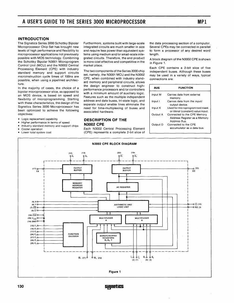
A USER'S GUIDE TO THE SERIES 3000 MICROPROCESSOR
INTRODUCTION The Signetics Series 3000 Schottky Bipolar Microprocessor Chip Set has brought new levels of high performance and flexibility to microprocessor applications not previously possible with MOS technology. Combining the Schottky Bipolar N3001 Microprogram Control Unit (MCU) and the N3002 Central Processing Element (CPE) with industry standard memory and support circuits microinstruction cycle times of 100ns are possible, when using a pipelined architecture. In the majority of cases, the choice of a bipolar microprocessor slice, as opposed to an MOS device, is based on speed and flexibility of microprogramming. Starting with these characteristics, the design of the Signetics Series 3000 Microprocessor has been optimized to achieve the following objectives:
• Logic replacement capability • Higher performance in terms of speed • Industry standard memory and support chips • Cooler operation • Lower total system cost
(12~
Furthermore, systems built with large-scale integrated circuits are much smaller in size and require less power than equivalent systems using medium and/or small-scale integrated circuits. Therefore, the end product is more cost effective and competitive in the market place.
The two components of the Series 3000 chip set, namely, the N3001 MCU and the N3002 CPE, when combined with industry standard memory and peripheral circuits, allows the design engineer to construct highperformance processors and/or controllers with a minimum amount of-auxiliary logic .. Features such as the multiple independent address and data buses, tri-state logic, and separate output enable lines eliminate the need for time-multiplexing of buses and associated hardware.
DESCRIPTION OF THE N3002 CPE Each N3002 Central Processing Element (CPE) represents a complete 2-bit slice of
N3002 CPE BLOCK DIAGRAM
(13) (20) (19)
MPI
the data processing section of a computer. Several CPEs may be connected in parallel to form a processor of any desired word length.
A block diagram of the N3002 CPE is shown in Figure 1.
Each CPE contains a 2-bit slice of five independent buses. Although these buses may be used in a variety of ways, typical connections are:
BUS FUNCTION
Input M Carries data from external memory.
Input I Carries data from the input! output device.
Input K Used for microprogrammed mask or literal (constant) value input.
Output A Connected to the CPE Memory Address Register as a Memory Address Bus.
Output D Connected to the CPE accumulator as a data bus.
r--------t~--1~----------~~--1:----------------l
130
I (11) ~ - I EA
(5) X
(6) Y
(7) CO
(9) LI
(1B) ClK
(28) VCC
(14) GND
(15) F,
(16) Fs
(17) F,
(24) F,
(27) F,
(26) F,
(25) Fo
I I
I I I I I I I I -
.J
~ ~
I
~
I I
. OUTPUT BUFFER
1 MEMORY ADDRESS REGISTER
t +
FUNCTION DECODER
L ____________
I L L OUTPUT BUFFER I
1 +
I 1 T
I AC REGISTER I ! •
I I I 1 T
ARITHMETIC AND J.,
lOGIC UNIT
t t t t
I MULTIPLEXER J I MULTIPLEXER I A B
~ II tt i~
1
I I SCRATCHEDPAD REGISTERS
Ro-R •• T
t +
1,---. ------------, , -- r1 r------------.J
-iiii 21 22 M , ( ) 0 ( ) I, 10 K, Ko
(2) (1) (4) (3)
Figure 1
S!!)OOtiCS
E D
(23)
CI (10)
RO (3)
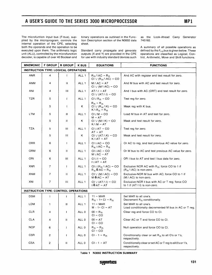
A USER'S GUIDE TO THE SERIES 3000 MICROPROCESSOR MPI
The microfuntion input bus (F-bus), supplied by the microprogram, controls the internal operation of the CPE, selecting both the operands and the operation to be executed upon them. The arithmetic logic unit (ALU), controlled by the microfunction decoder, is capable of over 40 Boolean and
MNEMONIC F GROUP R GROUP
binary operations as outlined in the Function Description section of the N3002 data sheet.
Standard carry propagate and generate outputs (X and Y) are provided in the CPE for use with industry standard devices such
K BUS EQUATIONS
as the Look-Ahead Carry Generator 74S182.
A summary of all possible operations as defined by the FO-6 bus is given below. These operations are classified as Logical, Control, Arithmetic, Move and Shift functions.
FUNCTIONS
INSTRUCTION TYPE: LOGICAL OPERATIONS
ANR 4 I ALL 1 Rn!\AC ..... Rn And AC with register and test result for zero. CI V (Rn!\AC) ..... CO
ANM 4 II ALL 1 M!\AC ..... AT And M bus with AC and test result for zero. CI V (M!\AC) ..... CO
ANI 4 III ALL 1 AT!\I ..... AT And I bus with AC (ORT) and test result for zero. CI V (AT!\I) ..... CO
TZR 5 I ALL 1 CIVR n ..... CO Test reg for zero.
Rn ..... Rn 5 I K CI V (Rn !\K) ..... CO Mask reg with K bus.
K!\Rn ..... Rn
LTM 5 II ALL 1 CIVM ..... CO Load M bus in AT and test for zero. M ..... AT
5 II K CI V (M/\K) ..... CO Mask and test result for zero. K!\M ..... AT
TZA 5 III ALL 1 CIVAT ..... CO Test reg for zero. AT ..... AT
5 III K CI V (AT !\K) ..... CO Mask and test result for zero. K!\AT ..... AT
ORR 6 I ALL 1 CIVAC ..... CO Or AC to reg, and test previous AC value for zero. Rn VAC ..... Rn
ORM 6 II ALL 1 CIVAC ..... CO Or M bus to AC and test previous AC value for zero. MVAC ..... AT
ORI 6 III ALL 1 CIVI ..... CO OR I bus to AT and test I bus data for lero. IVAT ..... AT
XNR 7 I ALL 1 CIV(Rn!\AC) ..... CO Exclusive NOR AC with R n; force CO to 1 if Rn E9AC ..... Rn (R n!\AC) is non-zero.
XNM 7 II ALL 1 CI V (M!\AC) ..... CO Exclusive-NOR M bus with AC; force CO to 1 if ME9AC ..... AT (M!\AC) is non-zero.
XNI 7 III ALL 1 CI V (AT!\ I) ..... CO Exclusive-NOR I bus with AC or T reg; force CO I eAT ..... AT to 1 if (AT /\ I) is non-zero.
INSTRUCTION TYPE: CONTROL OPERATIONS
DSM 1 I ALL 1 11 ..... MAR Set MAR to all one's. R n -1+CI ..... Rn Decrement R n conditionally.
LDM 1 II ALL 1 11 ..... MAR Set MAR to all one's. M-1+CI ..... AT Load conditionally decremented M bus in AC or T reg.
CLR 4 I ALL 0 00 ..... Rn Clear reg and force CO to CI. CI ..... CO
CLA 4 II ALL 0 00 ..... AT Clear AC or T and force CO to CI. CI ..... CO
NOP 6 I ALL 0 Rn ..... Rn Null operation and force CO to CI. CI ..... CO
CSR 2 I ALL 0 CI-1 ..... Rn Conditionally clear or set R n to all O's or 1 's, respectively.
CSA 2 II ALL 0 CI - 1 ..... AT Conditionally clear or set AC arT reg to all O's or 1 's, respectively.
Table 1 N3002 INSTRUCTION SUMMARY
S!!)DotiCS 131
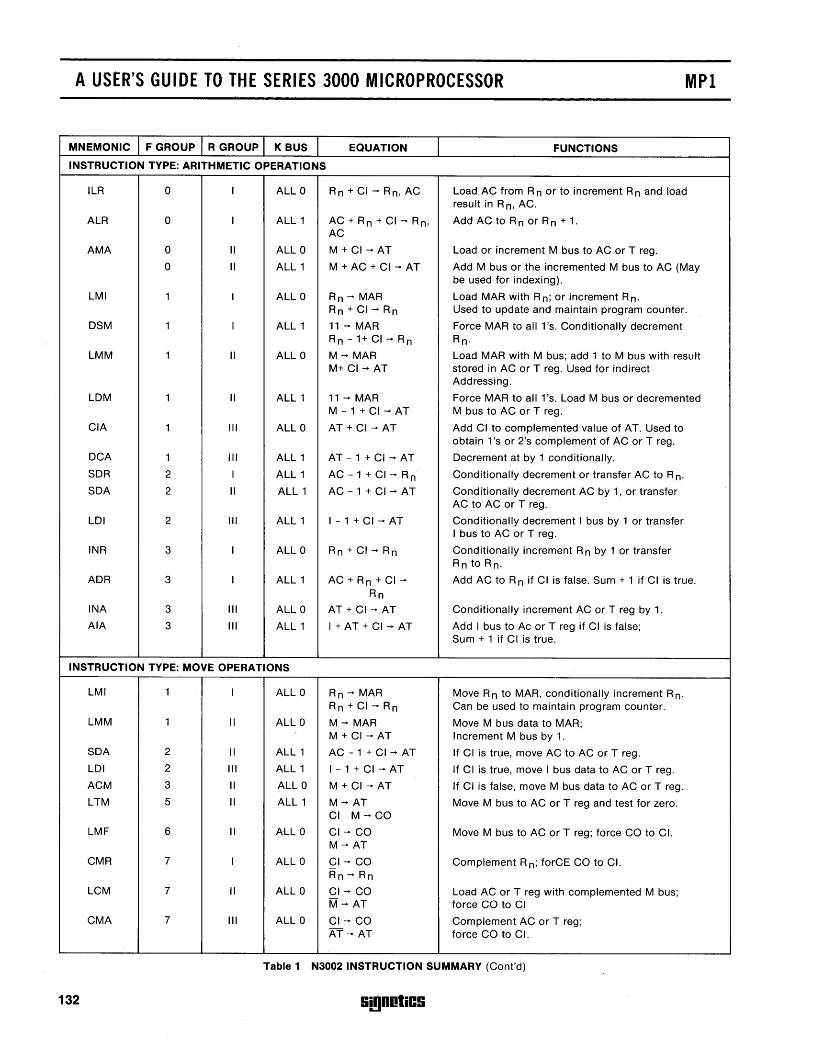
A USER'S GUIDE TO THE SERIES 3000 MICROPROCESSOR MPI
MNEMONIC F GROUP R GROUP K BUS EQUATION FUNCTIONS
INSTRUCTION TYPE: ARITHMETIC OPERATIONS
ILR 0 I ALL 0 Rn+C; ..... Rn,AC Load AC from R n or to increment R n and load result in R n, AC.
ALR 0 I ALL 1 AC + Rn + CI ..... Rn, Add AC to R n or R n + 1. AC
AMA 0 II ALL 0 M + CI ..... AT Load or increment M bus to AC or T reg.
0 II ALL 1 M + AC + CI ..... AT Add M bus or the incremented M bus to AC (May be used for indexing).
LMI 1 I ALL 0 Rn ..... MAR Load MAR with R n; 0 r increment R n. Rn+CI ..... Rn Used to update and maintain program counter.
DSM 1 I ALL 1 11 ..... MAR Force MAR to all 1 'so Conditionally decrement Rn - 1+ CI ..... Rn Rn·
LMM 1 II ALL 0 M ..... MAR Load MAR with M bus; add 1 to M bus with result M+ CI ..... AT stored in AC or T reg. Used for indirect
Addressing.
LDM 1 II ALL 1 11 ..... MAR Force MAR to all 1 'so Load M bus or decremented M - 1 + CI ..... AT M bus to AC or T reg.
CIA 1 III ALL 0 AT + CI ..... AT Add CI to complemented value of AT. Used to obtain 1 's or 2's complement of AC or T reg.
DCA 1 III ALL 1 AT - 1 + CI ..... AT Decrement at by 1 conditionally.
SDR 2 I ALL 1 AC-1+CI ..... Rn Conditionally decrement or transfer AC to R n.
SDA 2 II ALL 1 AC - 1 + CI ..... AT Conditionally decrement AC by 1, or transfer AC to AC or T reg.
LDI 2 III ALL 1 1-1 + CI .... AT Conditionally decrement I bus by 1 or transfer I bus to AC or T reg.
INR 3 I ALL 0 Rn+CI ..... Rn Conditionally increment R n by 1 or transfer Rn to R n.
ADR 3 I ALL 1 AC+Rn+CI ..... Add AC to R n if CI is false. Sum + 1 if CI is true. Rn
INA 3 III ALL 0 AT + CI ..... AT Conditionally increment AC or T reg by 1.
AlA 3 III ALL 1 I + AT + CI ..... AT Add I bus to Ac or T reg if CI is false; Sum + 1 if CI is true.
INSTRUCTION TYPE: MOVE OPERATIONS
LMI 1 I ALL 0 Rn ..... MAR Move R n to MAR, conditionally increment R n. Rn+CI ..... Rn Can be used to maintain program counter.
LMM 1 II ALL 0 M .... MAR Move M bus data to MAR; M + CI ..... AT Increment M bus by 1.
SDA 2 II ALL 1 AC - 1 + CI ..... AT If CI is true, move AC to AC or T reg.
LDI 2 III ALL 1 1-1 + CI ..... AT If CI is true, move I bus data to AC or T reg.
ACM 3 II ALL 0 M + CI .... AT If CI is false, move M bus data to AC or T reg.
LTM 5 II ALL 1 M .... AT Move M bus to AC or T reg and test for zero. CI M ..... CO
LMF 6 II ALL 0 CI ..... CO Move M bus to AC or T reg; force CO to CI. M .... AT
CMR 7 I ALL 0 CI ..... CO Rn ..... Rn
Complement R n; forCE CO to CI.
LCM 7 II ALL 0 CI ..... CO Load AC or T reg with complemented M bus; M ..... AT force CO to CI
CMA 7 III ALL 0 CI ..... CO Complement AC or T reg; AT ..... AT force CO to CI.
Table 1 N3002 INSTRUCTION SUMMARY (Cont'd)
132 !i!!lDotiC!i
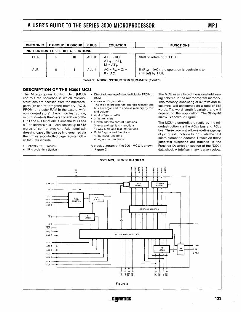
A USER'S GUIDE TO THE SERIES 3000 MICROPROCESSOR MPI
MNEMONIC F GROUP R GROUP K BUS EQUATION FUNCTIONS
INSTRUCTION TYPE: SHIFT OPERATIONS
SRA 0 III ALL 0 ATL - RO Shift or rotate right 1 BIT. ATH - ATL LI - ATH
ALR 0 I ALL 1 AC + Rn + CI - If (R n) = (AG), the operation is equivalent to R n, AC shift left by 1 bit.
Table 1 N3002 INSTRUCTION SUMMARY (Cont'd)
DESCRIPTION OF THE N3001 MCU The Microprogram Control Unit (MCU) controls the sequence in which microinstructions are acessed from the microprogarm (or control program) memory (ROM, PROM, or bipolar RAM in the case of writable control store). Each microinstruction, in turn, controls the overall operation of the CPU and I/O functions. Since the MCU has a 9-bit address bus, it can access up to 512 words of control program. Additional addressing capability can be implemented via the firmware-controlled page register. Other features include:
• Schottky TTL Process • 45ns cycle time (typical)
FO
ERA
EN f
FCO
FC1
FC2
FC3
FLAG CONTROL H
I F ~
I lATCH FI
• Direct addressing of standard bipolar PROM or ROM
• advanced Organization: The 9-bit microprogram address register and bus are organized to address memory by row and column.
• 4-bit program Latch • 2 flag registers • Eleven address control functions:
3 jump and test latch functions 16 way jump and test instructions
• Eight flag control functions: 4 flag input functions 4 flag output functions
A block diagram of the 3001 MCU is shown in Figure 2.
3001 MCU BLOCK DIAGRAM
The MCU uses a two-dimensional addressing scheme in the microprogram memory. This memory, consisting of 32 rows and 16 columns, will accommodate a total of 512 words. The word length is variable, and will depend on the application. The 32-by-16 matrix is shown in Figure 3.
The MCU is controlled directly by the microinstruction via the ACO-6 bus and FCo-3
bus. These two control buses define a group of jump/t~st functions to formulate the next microinstruction address. Details on these jump/test functions are outlined in the Function Description section of the N3001 data sheet. A brief summary is given below:
I I II f f I '- f
fa ROW eoc,", 1 OUTPUT OUTPUT
r
~ C.Z FLAGS
ADDRESS REGISTER
I- V /9
ISE lD
ClK
VCC
GNE
cr--c ! I
ACO
AC1
AC2
AC3
AC4
AC5
AC6
0-----.
~ 0-----. NEXT ADDRESS CONTROL
t
Figure 2
Si,gnotics
t h-I~ PR
lATCH
I~ I~ t~ I~
--0
--0
--0
PRO
PR1
PR2
133
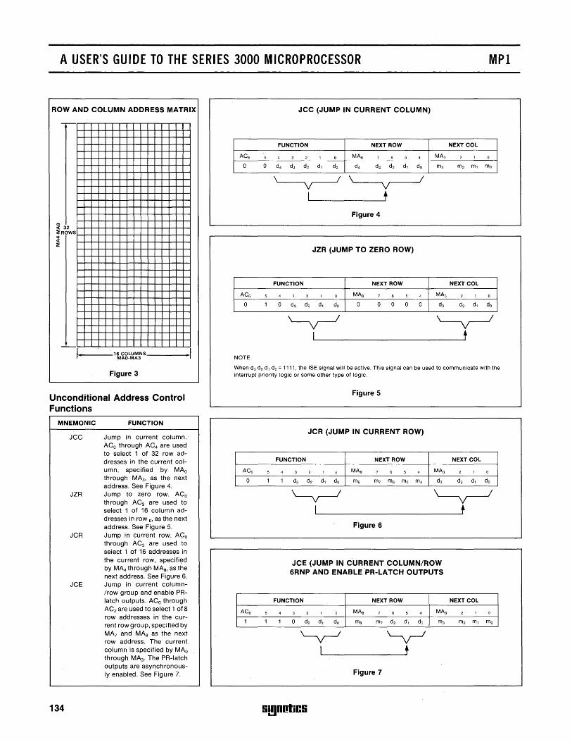
A USER'S GUIDE TO THE SERIES 3000 MICROPROCESSOR MPI
ROW AND COLUMN ADDRESS MATRIX
32 ROWS
Figure 3
Unconditional Address Control Functions
MNEMONIC
JCC
JZR
JCR
JCE
134
FUNCTION
Jump in current column.· ACo through AC4 are used to select 1 of 32 row addresses in the current column, specified by MAo through MA3 , as the next address. See Figure 4. Jump to zero row. ACo through AC3 are used to select 1 of 16 column addresses in row 0, as the next address. See Figure 5. Jump in current row. ACo through AC3 are used to select 1 of 16 addresses in the current row, specified by MA4 through MAs, as the next address. See Figure 6. Jump in current column/row group and enable PRlatch outputs. ACo through AC2 are used to select 1 of 8 row addresses in the current row group, specified by MA7 and MAs as the next row address. The current column is specified by MAo through MA3 . The PR-Iatch outputs are asynchronously enabled. See Figure 7.
JCC (JUMP IN CURRENT COLUMN)
FUNCTION NEXT ROW NEXT COL
AC6 5 4 3 2 1 0 MAa 7 6 5 4 MA3 2 1 0
0 0 d4 d3 d2 d1 do d4 d3 d2 d1 do m3 m2 m1 mo
Figure 4
JZR (JUMP TO ZERO ROW)
FUNCTION NEXT ROW NEXT COL
AC6 5 4 3 2 1 0 MAa 7 6 5 4 MA3 2 1 0
0 1 0 d3 d2 d1 do 0 0 0 0 0 d3 d2 d1 do
~ I
NOTE
When d3 d2 d1 do = 1111, the ISE signal will be active. This signal can be used to communicate with the interrupt priority logic or some other type of logic.
AC6
0
AC6
1
5
1
5
1
Figure 5
JCR (JUMP IN CURRENT ROW)
FUNCTION NEXT ROW
4
1
3 2 1 0 MAa 7 6 5 4 MA3
d3 d2 d1 do ma m7 m6 m5 m4 d3
~ I
Figure 6
JCE (JUMP IN CURRENT COLUMN/ROW 6RNP AND ENABLE PR-LATCH OUTPUTS
FUNCTION NEXT ROW
4 3 2 1 0 MAa 7 6 5 4 MA3
1 0 d2 d1 do ma m7 d2 d1 do m3
'--y---I I
Figure 7
!i!!]DotiC!i
NEXT COL
2 1 0
d2 d1 do
NEXT COL
2 1 0
m2 m1 mo
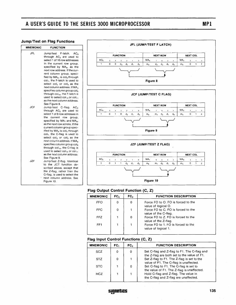
A USER'S GUIDE TO THE SERIES 3000 MICROPROCESSOR MPI
Jump/Test on Flag Functions
MNEMONIC FUNCTION
JFL Jump/test F-Iatch. ACo through AC3 are used to select 1 of 16 row addresses in the current row group, specified by MAs, as the next row add ress. If the cu rrent column group, specified by MA3, is colo through col?, the F-Iatch is used to select col2 or col3 as the next column address. If MA3 specifies column group cols through C0115, the F-Iatch is used to select COllO or COlll as the next column address.
JCF
JZF
See Figure 8. Jump/test C-flag. AC o through AC2 are used to select 1 of 8 row adresses in the current row group, specified by MA? and MAs, as the next row ad ress. If the current column group specified by MAs is colo through col?, the C-flag is used to select col2 or col3 as the next column address. If MA3 specifies column group cols through C0115, the C-flag is used to select COllO or COlll as the next column address. See Figure 9. Jump/test Z-flag. Identical to the JCT function described above, except that the Z-flag, rather than the C-flag, is used to select the next column address. See Figure 10.
JFL (JUMP/TEST F LATCH)
FUNCTION NEXT ROW NEXT COL
ACe 5 4 3 2 1 0 MAs 7 e 5 4 MA3 2 1 0
1 0 0 d3 d 2 d l do ms d3 d 2 d l do m3 0 1 f
~ I
Figure 8
JCF (JUMP/TEST C FLAG)
FUNCTION NEXT ROW NEXT COL
ACe 5 4 3 2 1 0 MAs 7 e 5 4 MA3 2 1 0
1 0 1 0 d 2 d l do ms m7 d 2 d l do m3 0 1 c
Figure 9
JZF (JUMP/TEST Z FLAG)
FUNCTION NEXT ROW NEXT COL
ACe 5 4 3 2 1 0 MA7 e 5 4 3 MA3 2 1 0
1 0 1 1 d 2 d l do ms m7 d 2 d l do m3 0 1 z
Figure 10
Flag Output Control Function (C, Z)
MNEMONIC FC3 FC2 FUNCTION DESCRIPTION
FFO 0 0 Force FO to O. FO is forced to the value of logical O.
FFC 0 1 Force FO to C. FO is forced to the value of the C-flag.
FFZ 1 0 Force FO to Z. FO is forced to the value of the Z-flag.
FF1 1 1 Force FO to 1. FO is forced to the value of logical 1.
Flag Input Control Functions (C, Z)
MNEMONIC FC1 FCo FUNCTION DESCRIPTION
SCZ 0 0 Set C-flag and Z-flag to F1. The C-flag and the Z-flag are both set to the value of F1.
STZ 0 1 Set Z-flag to F1. The Z-flag is set to the value of F1. The C-flag is unaffected.
STC 1 0 Set C-flag to F1. The C-flag is set to the value of F1. The Z-flag is unaffected.
HCZ 1 1 Hold C-flag and Z-flag. The value in the C-flag and Z-flag are unaffected.
Si!)DotiCS 135
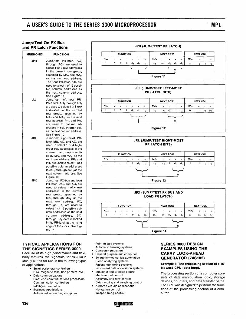
A USER'S GUIDE TO THE SERIES 3000 MICROPROCESSOR MPI
Jump/Test On PX Bus and PR Latch Functions
MNEMONIC FUNCTION
JPR
JLL
JRL
JPX
Jump/test PR-Iatch. ACo through AC2 are used to select 1 or 8 row addresses in the current row group, specified by MA7 and MAs, as the next row address. The four PR-Iatch bits are used to select 1 of 16 possible column addresses as the next column address. See Figure 11. Jump/test left-most PRlatch bits. ACo through AC2 are used to select 1 of 8 row addresses in the current row group, specified by MA7 and MAs, as the next row address. PR2 and PR3
are used to column addresses in col4 through col7 as the next column address. See Figure 12. Jump/test right-most PRlatch bits. ACo and AC, are used to select 1 of 4 highorder row addresses in the current row group, specified by MA7 and MAs, as the next row address. PRo and PRJ are used to select 1 of 4 possible column addresses in col'2 through col'5 as the next column address. See Figure 13. Jump/test PX-bus and load PR-Iatch. ACo and AC, are used to select 1 of 4 row addresses in the current row group, specified by MA6 through MAs, as the next row address. PX4 through PX7 are used to select 1 of 16 possible column addresses as the next column address. SXo through SX3 data is locked in the PR-Iatch at the rising edge of the clock. See Figure 14.
TYPICAL APPLICATIONS FOR THE SIGNETICS SERIES 3000 Because of its high performance and flexibility features, the Signetics Series 3000 is ideally suited for use in the following types of applications:
136
• Smart peripheral controllers Disk, magnetic tape, line printers, etc.
• Data communications Front end communications processors Communication controllers Intelligent terminals
• Business Applications Automated accounting computer
JPR (JUMP/TEST PR LATCH)
FUNCTION NEXT ROW NEXT COL
ACs 5 4 3 2 , 0 MAs 7 s 5 4 MA3 2 , 0
1 1 0 0 d2 d, do ms m7 d2 d, do P3 P2 p, Po
Figure 11
JLL (JUMP/TEST LEFT-MOST PR LATCH BITS)
FUNCTION NEXT ROW NEXT COL
ACs 5 4 3 2 , 0 MAs 7 s S 4 MA3 2 , 0
1 1 0 1 d2 d, do ms m7 d2 d, do 0 1 P3 P2
Figure 12
JRL (JUMP/TEST RIGHT-MOST PR LATCH BITS)
FUNCTION
ACs s 4 3
1 1 1 1
2
1
, 0
d, do
'---v--I I
NEXT ROW NEXT COL
MAs 7 s 5 4 MA3 2 , 0
me m7 1 d, do 1 1 p, Po
Figure 13
JPX (JUMP/TEST PX BUS AND LOAD PR LATCH)
FUNCTION
ACs 5 4 3 2 , 0
1 1 1 1 0 d, do
'--y--I I
Point of sale systems Automatic banking systems
• Computer emulation • General purpose minicomputer • Scientific/medical lab automation
Blood analyzing systems Patient monitoring systems Instrument data acquisition systems
• Industrial and process control Machine tool control Assembly line flow control Batch mixing and weighing control
• Airborne vehicle applications Navigation control Weapon firing control
!i!!lDotiC!i
NEXT ROW NEXT COL
MAe 7 s S 4 MA3 2 , 0
me m7 ms d, do X7 Xs Xs X4
Figure 14
SERIES 3000 DESIGN EXAMPLES USING THE CARRY LOOK-AHEAD GENERATOR (74S182) Example 1: The processing section of a 16-bit word CPU (data loop).
The processing section of a computer consists of data manipulation logic, storage devices, counters, and data transfer paths. The ePE was designed to perform the functions of the processing section of a computer.
A USER'S GUIDE TO THE SERIES 3000 MICROPROCESSOR MPI
To obtain low cost and high performance design, parallel carry look-ahead can be implemented using the multi-source industry standard part, 748182. For a 16-bit CPU configuration, 8 CPE arrays, one MCU, and a 2 stage carry look-ahead generator can be connected as shown in Figure 15. Note that the three state gate 8T95 is disabled by the detection of a 8hift Right operation (8RA); hence, its outputto the FI input of the 3001 is placed in a high impedance state. The 8RA operation is detected by the 6-input NAND function. The data, address and function buses are not shown in Figure 15, and the following logic state definition is observed:
N3002 K bus Active Low I bus Active Low M bus Active Low D bus Active Low A bus Active Low LI, RO, CI Active Low X, Y Active High
N3001 FI, FO Active Low
74S182 PO-P3 (XO-3) Active High GO-G 3 (Y 0-3) Active High P, G (X, Y) Active High C n Acitve Low C n+x, C n+y , C n+z Active Low
Depending on the availability of spare gates, the same processing section (or data loop) can be implemented as shown in Figure 15. The active state of all data buses and other signals is similar to the example shown in Figure 15. Notethatthe8hiftRight operation again inhibits the Carry via the 74808 gate. The 74805 is used due to its open collector type output which can be connected to the FI input of the N3001. The pull up is 470 n to +5V.
CARRY lOOK- TYP-
OTHER AHEAD ICAl MAX lOGIC 745182 (ns) (ns)
- 1st Stage 7 10.5 - 2nd Stage 4.5 7
8T95 - 6 7.5 N3002 TXD - 18 33
TOTAL DELAY THROUGH DATA LOOP 35.5 (TYP), 58ns (MAX)
Table 2 PROPAGATION DELAY ANALYSIS FOR FIGURE 15,
EXAMPLE A
The propagation delaY' through the two stages of 748182 is analyzed as follows:
lOOK- TYP-OTHERS AHEAD ICAl MAX
1st stage 7ns 10.5ns 74S08 7ns 7.5ns
2nd stage 4.5ns 7.0ns 74S05 5ns 7.5ns 74S05 5ns 7.5ns N3002 TXD 18ns 33.0ns
Total Delay 46.5ns 73.0ns
Example 2: The control section of a 16-Bit Word CPU (control loop) The control section of a microprogrammed processor usually performs the following functions:
• Decodes machine instructions • Controls ALU functions (in N3002) • Controls data paths • Updates CPU hardware status • Initiates I/O or memory operations • Other miscellaneous control functions
The N3001 MCU, ROM/PROM (8ignetics 828115,828114, etc.) and minimum additional logic (such as gates, FF's or the 8ignetics' FPLA) can be used to implement the
control section of the CPU. A simplified logic diagram of the control section is shown in Figure 16.
For a microprogrammed CPU, one of the most important design efforts is in the definition of the microinstruction (microword). In general, the microinstruction consists of a number of control fields to handle the following functions:
• Initiation of main memory operations • Initiation of I/O operations • Instruction decoding • Manipulation data transfer • Testing machine status • Responding to and processing interrupts • Address sequencing
When all the possible and necessary control functions are defined, then the microword can be structured. The following structure is an attempt to define a 32-bit microword that fulfills the above-mentioned control functions (Figure 17).
When defining the microword, it is essential to compact each field as muchas possible without sacrificing efficiency. To illustrate this principle, a format field is supplied which defines multiple usage of the lower order 9 bits, K < 8 > and K < 7:0 > of the microword. The formats are classified as shown in Table 3.
CONTROL SECTION OF CPU
(MICRO-INSTRUCTION 32 BITS)
MACRO INSTRUCTIONS STATUS
(FROM MAIN MEMORY)
Figure 16
lii!)DotiCIi 137
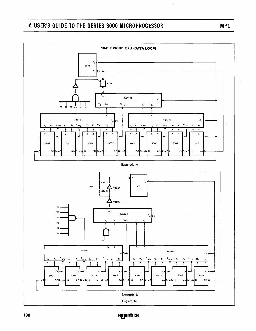
A USER'S GUIDE TO THE SERIES 3000 MICROPROCESSOR
FO
3001
F1
1111 I I F6 F5 F4 F3 F2 F1
74S182
Y, x, C n +z y, x, C n+y Y, x,
t t 0 t t 0 t t Y x Y x Y x
3002 3002 3002
I'" flO P-c LI flO p.-C LI flO
+5V
F6
F5
F4
F3
F2
F1
74S182
138
16-BIT WORD CPU (DATA LOOP)
8T95
C n+y
Y 1 X
1
t t Y x
C n+x Yo
0 t Y
p-< LI
74S182
C n+x Yo
t Y
C n P-Xo Y, x, Cn+z
t t t 0 x Y x p.
3002 3002
flO p--..C LI flO p.-c LI
Example A
FI
FO
3001 74S05
74S05
74S182
P, Cn+x Go
G
Example B
Figure 15
S!!)DotiCS
Cn
Po
C n
Xo
t X
Y, x,
t 1 Y x
3002
flO
74S182
C n+y
J Io--c LI
MPI
C n
Y, x, C n+x Yo Xo
t t J t t Y x Y x
3002 3002
flO P--c LI flO
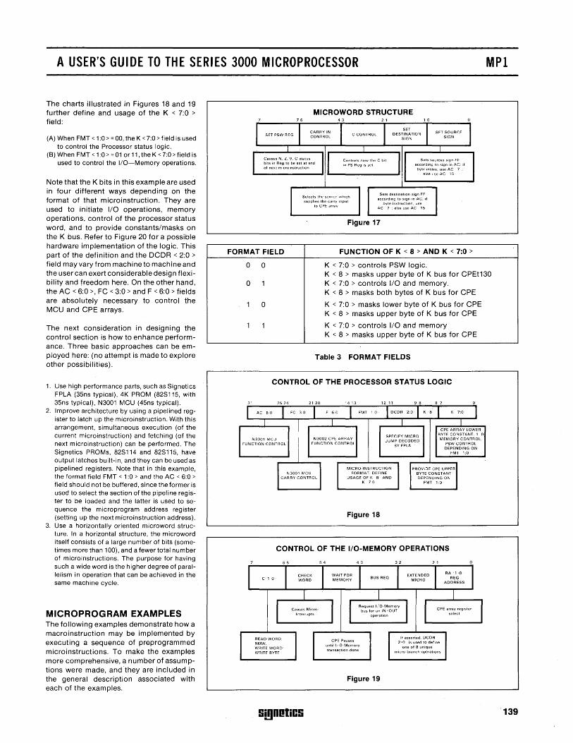
A USER'S GUIDE TO THE SERIES 3000 MICROPROCESSOR MPI
The charts illustrated in Figures 18 and 19 further define and usage of the K < 7:0 >
field:
(A) When FMT < 1:0> = 00, the K < 7:0 > field is used to control the Processor status logic.
(8) When FMT < 1:0> = 01 or 11, the K < 7:0 > field is used to control the I/O-Memory operations.
Note that the K bits in this example are used in four different ways depending on the format of that microinstruction. They are used to initiate I/O operations, memory operations, control of the processor status word, and to provide constants/masks on the K bus. Refer to Figure 20 for a possible hardware implementation of the logic. This part of the definition and the DCDR < 2:0 >
field may vary from machine to machine and the user can exert considerable desig n flexibility and freedom here. On the other hand, the AC < 6:0 >, FC < 3:0 > and F < 6:0 > fields are absolutely necessary to control the MCU and CPE arrays.
The next consideration in designing the control section is how to enhance performance. Three basic approaches can be employed here: (no attempt is made to explore other possibilities).
1. Use high performance parts, such as 8ignetics FPLA (35ns typical), 4K PROM (828115, with 35ns typical), N3001 MCU (45ns typical).
2. Improve architecture by using a pipelined register to latch up the microinstruction. With this arrangement, simultaneous execution (of the current microinstruction) and fetching (of the next microinstruction) can be performed. The 8ignetics PROMs, 828114 and 828115, have output latches built-in, and they can be used as pipelined registers. Note that in this example, the format field FMT < 1 :0 > and the AC < 6:0 > field should not be buffered, since the former is used to select the section of the pipeline register to be loaded and the latter is used to sequence the microprogram address register (setting up the next microinstruction address).
3. Use a horizontally oriented microword structure. In a horizontal structure, the microword itself consists of a large number of bits (sometimes more than 100), and a fewer total number of microinstructions. The purpose for having such a wide word is the higher degree of parallelism in operation that can be achieved in the same machine cycle.
MICROPROGRAM EXAMPLES The following examples demonstrate how a macroinstruction may be implemented by executing a sequence of preprogrammed microinstructions. To make the examples more comprehensive, a number of assumptions were made, and they are included in the general description associated with each of the examples.
MICROWORD STRUCTURE
bits In Reg to be set at end of next microinstruction
In PS Reg is set
Selects the SOllIe!'! which supplies the carry Input
to ePE array
Sets destination Sign FF according to sign in AC, If
byte instruction. LIse AC 7. else use AC 15
Figure 17
FORMAT FIELD FUNCTION OF K < 8 > AND K < 7:0 >
0 0 K < 7:0 > controls PSW logic. K < 8 > masks upper byte of K bus for CPEt130
0 1 K < 7:0 > controls I/O and memory. K < 8 > masks both bytes of K bus for CPE
1 0 K < 7:0 > masks lower byte of K bus for CPE K < 8 > masks upper byte of K bus for CPE
1 1 K < 7:0 > controls I/O and memory K < 8 > masks upper byte of K bus for CPE
Table 3 FORMAT FIELDS
CONTROL OF THE PROCESSOR STATUS LOGIC
31 2524 21 20 1413 12 11 98 8 7
I AC 60 I FC 3.0 I F 6,0 I FMT 10 I DC DR 2,0 I K 8 I K 7,0 I I I I I
CPE ARRAY LOWER
SPECIFY MICRO BYTE CONSTANT; 1 0 N3001 MCU N3002 CPE ARRAY
JUMP OECODED MEMORY CONTROL. FUNCTION CONTROL FUNCTION CONTROL
BY FPLA PSW CONTROL
N3001 MCI) CARRY CONTROL
MICRO·INSTRUCTION FORMAT. DEFINE
USAGE OF K 8 K 70
Figure 18
DEPENDING ON FMT
PROVIDE CPE UPPER BYTE CONSTANT DEPENDING ON
FMT LO
1.0
CONTROL OF THE I/O-MEMORY OPERATIONS
READ WORD; RMW. WRITE WORD· WRITE BYTE
Si!lDotiCS
ePE Pauses untill/O-Memory transaction done
Figure 19
If asserted, DeDR 2""0 is used to define
one of 8 unique micro-branch operations
139
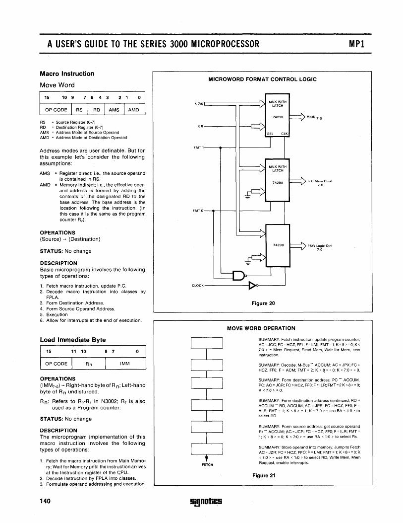
A USER'S GUIDE TO THE SERIES 3000 MICROPROCESSOR MPI
Macro Instruction
Move Word
15 10 9 7 6 4 3 2 1 o
OP CODE I RS I RD I AMS I AMD
RS = Source Register (0-7) RD = Destination Register (0-7) AMS = Address Mode of Source Operand AMD = Address Mode of Destination Operand
Address modes are user definable. But for this example let's -consider the following assumptions: .
AMS = Register direct; i.e., the source operand is c-ontained in RS.
AMD = Memory indirect; i.e., the effective operand address is formed by adding the contents of the designated RD to the base address. The b~se address is the location following the instruction. (In this case it is the same as the program counter R7)'
OPERATIONS (Source) -- (Destination)
STATUS: No change
DESCRIPTION Basic microprogram involves the following types of operations:
1. Fetch macro instruction, update P.C. 2. Decode macro instruction into classes by
FPLA. 3. Form Destination Address. 4. Form Source Operand Address. 5. Exec;ution . 6. Allow for interrupts at the end of execution.
Load Immediate Byte
15 11 10 8 7 o
OP CODE I Rn I IMM
OPI;RATIONS (IMM7-o) -- Right-hand byte of R n; Left-hand byte of R n undisturbed.
R n: Refers to Ro-R7 in N3002; R7 is also used as a Program counter.
STATUS: No change
Or;:SCRIPTION The microprogram implementation of this macro instruction involves the following types of operations:
1. Fetch the IT]acro instruction from Main Memory; Wait for Memory until the instruction arrives at the Instruction register of the GPU.
2. Decode instruction by FPLA into classes. 3. Formulate operand addressing ~nd execution.
140
MICROWORD FORMAT CONTROL LOGIC
K 7:0 L..-____ -, r---t./
Mask 7-0
K 8 ----,----j
ClK
FMT1--~~~~ ~----~
FMT 0 - ___ --+--~
74298
I/O-Mem Ctrol 7-0
PSW l09ic Ctrl 7-0
CLOCK ---------1 ~>_---~
FETCH
SmDOliCS
Figure 20
MOVE WORD OPERATION
SUMMARY: Fetch instruction; update program counter; AC = JCC; FC = HCZ, FF1; F = LMI; FMT = 1; K < 8 > = 0; K <
7:0 > = Mem Request, Read Mem, Wait for Mem, new instruction.
SUMMARY: Decode; M-Bus - ACCUM; AC = JPX; FC = HCZ, FFO; F = ACM;' FMT = 2; K < 8 > = 0; K < 7:0 > = O.
SUMMARY: Form destination address; PC - ACCUM, PC; AC = JCR; FC = HCZ, FFO; F = ILR; FMT = 2 K < 8 > = 0; K < 7:0> = O.
SUMMARY: Form destination address continued; RD + ACCUM - RD, ACCUM; AC = JPR; FC = HCZ, FFO; F = ALR; FMT = 1; K < 8 > = 1; K < 7:0 > = use RA < 1:0 > to select RD_
SUMMARY: Form source address; get source operand Rs- ACCUM; AC = JCR; FC - HCZ, FFO; F = ILR; FMT = 1; K < 8 > = 0; K < 7:0 > = use RA < 1:0 > to select Rs.
SUMMARY: Store operand into memory; Jump to Fetch AC = JZR; FC = HCZ, FFO; F = LMI; FMT = 1; K < 8 > = 0; K < 7:0> = use RA < 1:0 > to select RD; Write Mem, Mem Request, enable interrupts.
Figure 21
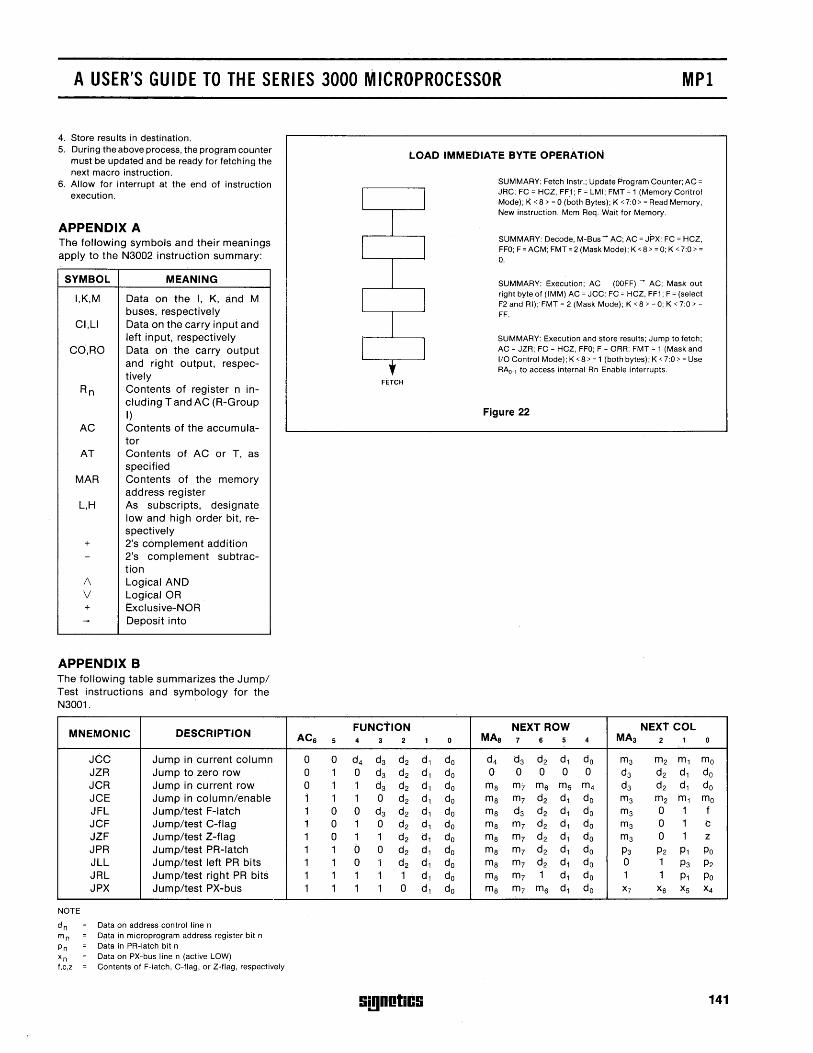
A USER'S GUIDE TO THE SERIES 3000 MICROPROCESSOR MPI
4. Store results in destination. 5. During the above process, the program counter
must be updated and be ready for fetching the next macro instruction.
6. Allow for interrupt at the end of instruction execution.
APPENDIX A The following symbols and their meanings apply to the N3002 instruction summary:
SYMBOL MEANING
I,K,M Data on the I, K, and M buses, respectively
CI,L! Data on the carry input and left input, respectively
CO,RO Data on the carry output and right output, respectively
R n Contents of register n including T and AC (R-Group I)
AC Contents of the accumulator
AT Contents of AC or T, as specified
MAR Contents of the memory address register
L,H As subscripts, designate low and high order bit, respectively
+ 2's complement addition - 2's complement subtrac-
tion 1\ Logical AND V Logical OR + Exclusive-NOR -+ Deposit into
APPENDIX B The following table summarizes the Jump/ Test instructions and symbology for the N3001.
MNEMONIC DESCRIPTION
JCC Jump in current column JZR Jump to zero row JCR Jump in current row JCE Jump in column/enable JFL Jump/test F-Iatch JCF Jump/test C-flag JZF Jump/test Z-flag JPR Jump/test PR-Iatch JLL Jump/test left PR bits JRL Jump/test right PR bits JPX Jump/test PX-bLis
NOTE
d n Data on address control line n m n Data in microprogram address register bit n Pn Data in PR-Iatch bit n xn Data on PX-bus line n (active LOW) f,c,z Contents of F-Iatch, C-flag, or Z-flag, respectively
ACs 5
0 0 0 1 0 1 i 1 1 0 1 0 1 0 1 1 1 1 1 1 1 1
LOAD IMMEDIATE BYTE OPERATION
SUMMARY: Fetch Instr.; Update Program COlJnter; AC =
I I JRC; FC = HCZ, FF1; F = LMI; FMT = 1 (Memory Control Mode); K < 8 > = 0 (both Bytes); K < 7:0 > = Read Memory,
I New instruction. Mem Req. Wait for Memory.
SUMMARY: Decode, M-Bus - AC; AC = JPX: FC = HCZ,
I I FFO; F = ACM; FMT=2 (Mask Mode); K < 8 > = 0; K < 7:0 > =
I O.
SUMMARY: Execution; AC (OOFF) - AC; Mask out
I I right byte of (IMM) AC = JCC: FC = HCZ, FF1; F = (select F2 and RI); FMT = 2 (Mask Mode); K < 8 > = 0; K < 7:0 > =
I FF.
SUMMARY: Execution and store results; Jump to fetch;
I I AC = JZR; FC = HCZ, FFO; F = ORR: FMT = 1 (Mask and , 1/0 Control Mode); K < 8 > = 1 (both bytes); K < 7:0 > = Use RAo., to access internal Rn Enable interrupts.
FETCH
Figure 22
FUNCTION NEXT ROW NEXT COL 4 3 2 1 0 MAs 7 s 5 4 MA3 2 1 0
d4 d3 d2 d1 do d4 d3 d2 d1 do m3 m2 m1 mo 0 d3 d2 d1 do 0 0 0 0 0 d3 d2 d1 do 1 d3 d2 d1 do ma m'r m6 ms m4 d3 d2 d1 do 1 0 d2 d1 do ma m7 d2 d1 do m3 m2 m1 mo 0 d3 d2 d1 do ma d3 d2 d1 do m3 0 1 f 1 0 d2 d1 do ma m7 d2 d1 do m3 0 1 c 1 1 d2 d1 do ma m7 d2 d1 do m3 0 1 Z
b 0 d2 d1 do ma m7 d2 d1 do P3 P2 P1 Po 0 1 d2 d1 do ma m7 d2 dj do 0 1 P3 P2 1 1 1 d1 do ma m7 1 d1 do 1 1 P1 Po 1 1 0 d1 do ma m7 m6 d1 do X7 X6 Xs X4
Si!lDotiCS 141
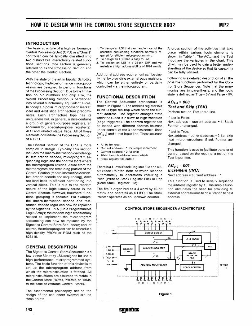
HOW TO DESIGN WITH THE CONTROL STORE SEQUENCER 8X02 MP2
INTROI)UCTION The basic structure of a high performance Central Processing Unit (CPU) or a "Smart" controller can be typically classified into two distinct but interactively related functional sections. One section is genp,rally referred to as the Processing Section and the other the Control Section.
With the state of the art in bipolar Schottky technology, high-performance microprocessors are designed to perform functions of the Processing Section. Due to the limitation on pin numbers and chip size, the overall Processing Section is partitioned into several functionally equivalent slices. In today's bipolar microprocessor market, 2-bit and 4-bit slice architecture predominates. Each architecture type has its uniqueness but, in general, a slice contains a group of general-purpose registers, an accumulator, special-purpose register(s), ALU and related status flags. All of these elements constitute the Processing Section of a CPU.
The Control Section of the CPU is more complex in design. Typically this section includes the macro-instruction decode logic, test-branch decode, microprogram sequencing logic and the control store where the microprogram resides. Aside from the microprogram, the remaining portion of the Control Section (macro instruction decode, test-branch decode and sequencing), does not lend itself to efficient partitioning into vertical slices. This is due to the random nature of the logic usually found in the Control Section. However, horizontal functional grouping is possible. For example, the macro-instruction decode and testbranch decode logic can now be replaced by the Signetics FPLA (Field Programmable Logic Array); the random logic traditionally needed to implement the microprogram sequencing can now be replaced by the Signetics Control Store Sequencer; and, of course, the microprogram can be stored in a high-density PROM or ROM such as the 82S115.
GENERAL DESCRIPTION The Signetics Control Store Sequencer is a low-power Schottky LS I, desig ned for use in high-performance, microprogrammed systems. The basic function of this device is to set up the microprogram address from which the microinstruction is fetched. All microinstructions are assumed to reside in the Control Store (ROMs, PROMs, or RAMs, in the case of Writable Control Store).
The fundamental philosophy behind the design of the sequencer evolved around three points.
142
1. To design an LSI that can handle most of the essential sequencing functions normally required for efficient microprogramming.
2. To design an LSI that is easy to use. 3. To design an LSI in a 28-pin DIP and yet
maintain a high addressability of 1024 words.
Additional address requirement can be easily met by providing external page registers, which can be either entirely or partially controlled via the microprogram.
FUNCTIONAL DESCRIPTION The Control Sequencer architecture is shown in Figure 1. The address register is a 10-bit D-type flip-flop which holds the current address. The register changes state when the Clock is in a low-to-high transition (edge-triggered). The address register can be loaded with different address sources under control of the 3 address control lines (AC2-o) and 1 test input line. These sources are:
• All Os for reset • Current address + 1 for simple increment • Current address + 2 for skip • 10-bit branch address from outside • Stack register file output
There is a 4-level Stack Register File and a 2-bit Stack Pointer, both of which respond automatically to operations requiring a Push (Write to Stack Register File) or Pop (Read Stack Register File).
The file is organized as a 4 word by 10-bit matrix and operates as a LIFO. The Stack Pointer operates as an up/down counter.
A cross section of the activities that take place within various logic elements is shown in Table 1. The AC2-o and the Test Input are the variables in the chart. This chart may be used to gain a better understanding of the device so that its capability can be fully utilized.
Following is a detailed description of all the possible functions performed by the Control Store Sequencer. Note that the mnemonics are in parenthesis, and the logic state is defined as True = 5V and False = OV.
AC2-0 = 000 Test and Skip (TSK) Perform test on Test Input line.
If test is False: Next address = current address + 1. Stack Pointer unchanged.
If test is True: Next address = current address + 2, i.e., skip next microinstructions. Stack Pointer unchanged.
This function is used to facilitate transfer of control based on the result of a test on the Test Input line.
AC2-0 = 001 Increment (INC) Next address = current address + 1.
This function is used to serially sequence the address register by 1. This simple function eliminates the need for providing 10 external address lines to do a Branch to next address.
CONTROL STORE SEQUENCER ARCHITECTURE
( I( )( )( )( )( )( )( )( )( )
A9 A, A, A, As A, A3 A, A, Ao
t--t·-t--r-+----------------,
( )
( )AC,
( )AC,
( )ACo
) CLK 0-1 Vcco--l GND <>--1
I I I L _____ _
B9 B, B, B, B, B, B3 B,. B, Bo ( )( )( )( )( )( )( )( )( )( )
Figure 1
Gi!)DotiCG
1-0 TEST
I () I
-----------------~
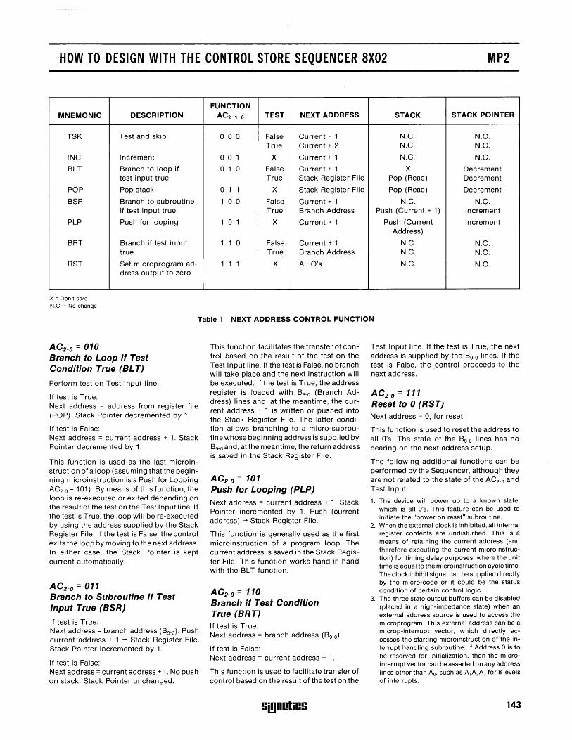
HOW TO DESIGN WITH THE CONTROL STORE SEQUENCER 8X02 MP2
MNEMONIC
TSK
INC
BLT
POP
BSR
PLP
BRT
RST
x = Don't care N.C. = No change
DESCRIPTION
Test and skip
Increment
Branch to loop if test input true
Pop stack
Branch to subroutine if test input true
Push for looping
Branch if test input true
Set microprogram ad-dress output to zero
FUNCTION AC21 0
000
001
o 1 0
011
100
1 o 1
1 1 0
1 1 1
TEST NEXT ADDRESS STACK STACK POINTER
False Current + 1 N.C. N.C. True Current + 2 N.C. N.C.
X Current + 1 N.C. N.C.
False Current + 1 X Decretnent True Stack Register File Pop (Read) Decrement
X Stack Register File Pop (Read) Decrement
False Current + 1 N.C. N.C. True Branch Address Push (Current + 1) Increment
X Current + 1 Push (Current Increment Address)
False Current + 1 N.C. N.C. True Branch Address N.C. N.C.
X AIIO's N.C. N.C.
Table 1 NEXT ADDRESS CONTROL FUNCTION
AC2-0 = 010 Branch to Loop if Test Condition True (BL T)
Perform test on Test Input line.
If test is True: Next address::: address from register file (POP). Stack Pointer decremented by 1.
If test is False: Next address::: current address + 1. Stack Pointer decremented by 1.
This function is used as the last microinstruction of a loop (assuming that the beginning microinstruction is a Push for Looping AC2-0 ::: 101). By means of this function, the loop is re-executed or exited depending on the result of the test on the Test Input line. If the test is True, the loop will be re-executed by using the address supplied by the Stack Register File. If the test is False, the control exits the loop by moving to the next address. In either case, the Stack Pointer is kept current automatically.
AC2-0 = 011 Branch to Subroutine if Test Input True (BSR)
If test is True: Next address::: branch address (B9-0). Push current address + 1 - Stack Register File. Stack Pointer incremented by 1.
If test is False: Next address::: current address + 1. No push on stack. Stack Pointer unchanged.
This function facilitates the transfer of control based on the result of the test on the Test Input line. If the test is False, no branch will take place and the next instruction will be executed. If the test is True, the address register is loaded with B9-0 (Branch Address) lines and, at the meantime, the current address + 1 is written or pushed into the Stack Register File. The latter condition allows branching to a micro-subroutine whose beginning address is supplied by B9-0 and, at the meantime, the return address is saved in the Stack Register File.
AC2-0 = 101 Push for Looping (PLP) Next address::: current address + 1. Stack Pointer incremented by 1. Push (current address) - Stack Register File.
This function is generally used as the first microinstruction of a program loop. The current address is saved in the Stack Register File. This function works hand in hand with the BL T function.
AC2-0 = 110 Branch if Test Condition True (BRT) If test is True: Next address::: branch address (B9-0).
If test is False: Next address::: current address + 1.
This function is used to facilitate transfer of control based on the result of the test on the
!ii!)DotiC!i
Test Input line. If the test is True, the next address is supplied by the B9-0 lines. If the test is False, the .. control proceeds to the next address.
AC2-0 = 111 Reset to 0 (RST) Next address::: 0, for reset.
This function is used to reset the address to all O's. The state of the B9-0 lines has no bearing on the next address setup.
The following additional functions can be performed by the Sequencer, although they are not related to the state of the AC2-0 and Test Input:
1. The device will power up to a known state, which is all a's. This feature can be used to initiate the "power on reset" subroutine.
2. When the external clock is inhibited, all internal register contents are undisturbed. This is a means of retaining the current address (and therefore executing the current microinstruction) for timing delay purposes, where the unit time is equal to the microinstruction cycle time. The clock inhibit signal can be supplied directly by the micro-code or it could be the status condition of certain control logic.
3. The three state output buffers can be disabled (placed in a high-impedance state) when an external address source is used to access the microprogram. This external address can be a microp-interrupt vector, which directly accesses the starting microinstruction of the interrupt handling subroutine. If Address a is to be reserved for initialization, then the microinterrupt vector can be asserted on any address lines other than AD, such as A1A2A3 for 8 levels of interrupts.
143
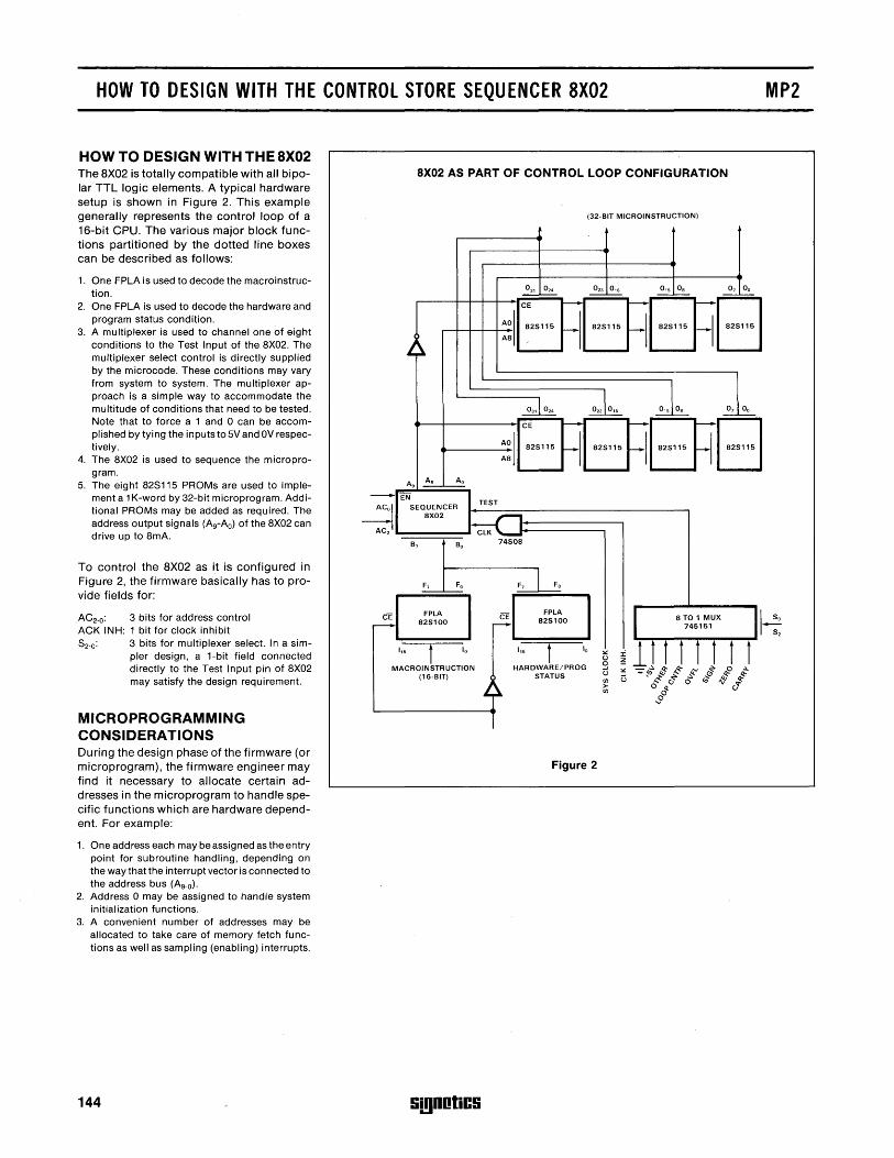
HOW TO DESIGN WITH THE CONTROL STORE SEQUENCER 8X02
HOW TO DESIGN WITH THE 8X02 The 8X02 is totally compatible with all bipolar TTL logic elements. A typical hardware setup is shown in Figure 2. This example generally represents the control loop of a 16-bit CPU. The various major block functions partitioned by the dotted line boxes can be described as follows:
1. One FPLA is used to decode the macroinstruction.
2. One FPLA is used to decode the hardware and program status condition.
3. A multiplexer is used to channel one of eight conditions to the Test Input of the 8X02. The multiplexer select control is directly supplied by the microcode. These conditions may vary from system to system. The multiplexer approach is a simple way to accommodate the multitude of conditions that need to be tested. Note that to force a 1 and 0 can be accomplished by tying the inputs to 5V and OV respectively.
4. The 8X02 is used to sequence the microprogram.
5. The eight 82S115 PROMs are used to implement a 1 K-word by 32-bit microprogram. Additional PROMs may be added as required. The address output signals (Ag-Ao) of the 8X02 can drive up to 8mA.
To control the 8X02 as it is configured in Figure 2, the firmware basically has to provide fields for:
AC2.0: 3 bits for address control ACK INH: 1 bit for clock inhibit S2-0: 3 bits for multiplexer select. In a sim
pler design, a 1-bit field connected directly to the Test Input pin of 8X02 may satisfy the design requirement.
MICROPROGRAMMING CONSIDERATIONS During the design phase of the firmware (or microprogram), the firmware engineer may find it necessary to allocate certain addresses in the microprogram to handle specific functions which are hardware dependent. For example:
1. One address each may be assigned as the entry point for subroutine handling, depending on the way that the interrupt vector is can nected to the address bus (Ag-o).
2. Address 0 may be assigned to handle system initialization functions.
3. A convenient number of addresses may be allocated to take care of memory fetch functions as well as sampling (enabling) interrupts.
144
8X02 AS PART OF CONTROL LOOP CONFIGURATION
(32·BIT MICROINSTRUCTION)
...--+--1--+--+-:-:1 ::: R :: ~I~~HI~~I
A As Ao 9 _'---
EN ACol SEQUENCER TEST
---::1 8X02 I 1"1 AC
2 ,,====;::= .. ~ .... --------,
l 74S08
B, I------BO
F, Fo ~
1'5
FPLA 82S100
MACROINSTRUCTION (16·BIT)
Si!lDotiCS
CE -piiiiiiiiiiiiiiii ____ _
1'5
FPLA B2S100
HARDWARE/PROG STATUS
Figure 2
::.: u 9 u rJ)
> rJ)
MP2
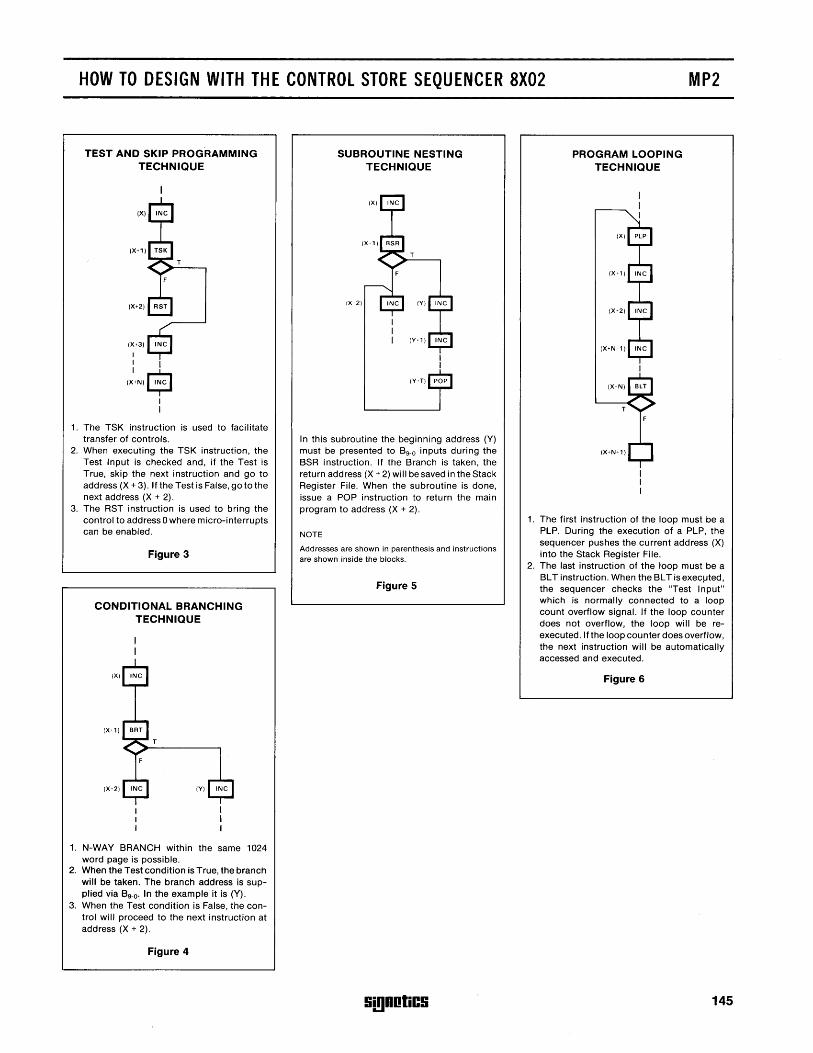
HOW TO DESIGN WITH THE CONTROL STORE SEQUENCER 8X02 MP2
TEST AND SKIP PROGRAMMING TECHNIQUE
(X)
(X+2)
(X+3) INC
I I I
(~+N)$ I I
1. The TSK instruction is used to facilitate transfer of controls.
2. When executing the TSK instruction, the Test Input is checked and, if the Test is True, skip the next instruction and go to address (X + 3). If the Test is False, go to the next address (X + 2).
3. The RST instruction is used to bring the control to address 0 where micro-interrupts can be enabled.
Figure 3
CONDITIONAL BRANCHING TECHNIQUE
1. N-WAY BRANCH within the same 1024 word page is possible.
2. When the Test condition is True, the branch will be taken. The branch address is supplied via B9-0. In the example it is (Y).
3. When the Test condition is False, the control will proceed to the next instruction at address (X + 2).
Figure 4
SUBROUTINE NESTING TECHNIQUE
In this subroutine the beginning address (Y) must be presented to B9-0 inputs during the BSR instruction. If the Branch is taken, the return address (X + 2) will be saved in the Stack Register File. When the subroutine is done, issue a POP instruction to return the main program to address (X + 2).
NOTE
Addresses are shown in parenthesis and instructions are shown inside the blocks.
Figure 5
Si!lDotiCS
PROGRAM LOOPING TECHNIQUE
1. The first instruction of the loop must be a PLP. During the execution of a PLP, the sequencer pushes the current address (X) into the Stack Register File.
2. The last instruction of the loop must be a BL T instruction. When the BL Tis exeq.Jted, the sequencer checks the "Test Input" which is normally connected to a loop count overflow signal. If the loop counter does not overflow, the loop will be reexecuted. If the loop counter does overflow, the next instruction will be automatically accessed and executed.
Figure 6
145
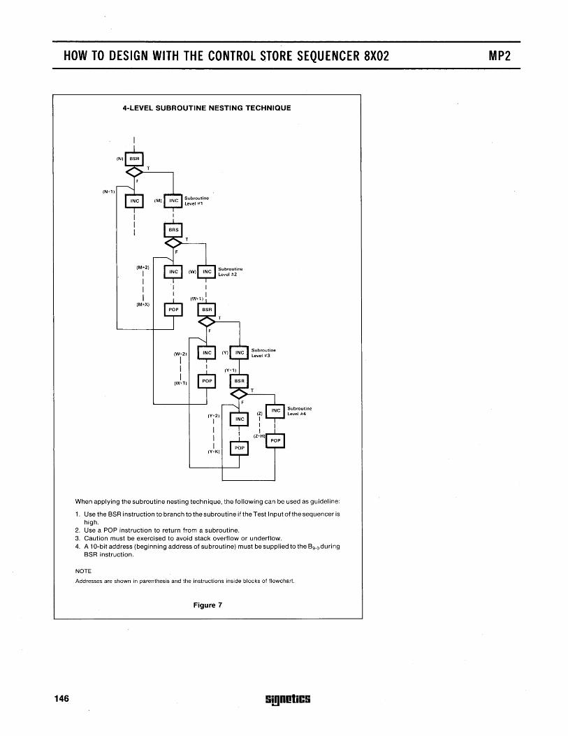
HOW TO DESIGN WITH THE CONTROL STORE SEQUENCER 8X02
146
4-LEVEL SUBROUTINE NESTING TECHNIQUE
(M+2)
I I I I
(M+X)
Subroutine Level #1
(W+2)
I I I
(W+T)
Subroutine Level #2
Subroutine Level #4
When applying the subroutine nesting technique, the following can be used as guideline:
1. Use the BSR instruction to branch to the subroutine if the Test Input of the sequencer is high.
2. Use a POP instruction to return from a subroutine. 3. Caution must be exercised to avoid stack overflow or underflow. 4. A 10-bit address (beginning address of subroutine) must be supplied to the B9. 0 during
BSR instruction.
NOTE
Addresses are shown in parenthesis and the instructions inside blocks of flowchart.
Figure 7
!ii!lDotiC!i
MP2
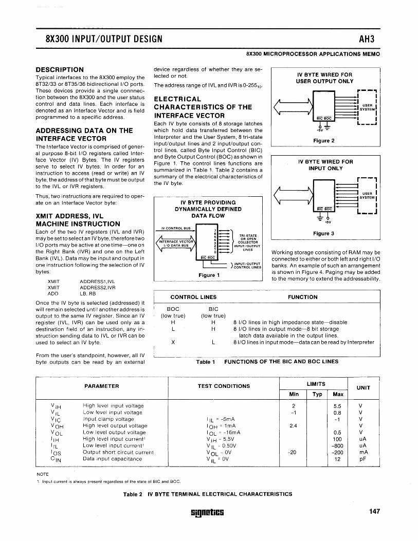
8X300 INPUT/OUTPUT DESIGN AH3
DESCRIPTION Typical interfaces to the 8X300 employ the 8T32/33 or 8T35/36 bidirectional I/O ports. These devices provide a single connnection between the 8X300 and the user status control and data lines. Each interface is denoted as an Interface Vector and is field programmed to a specific address.
ADDRESSING DATA ON THE INTERFACE VECTOR The Interface Vector is comprised of general purpose 8-bit I/O registers called Interface Vector (IV) Bytes. The IV registers serve to select IV bytes. In order for an instruction to access (read or write) an IV byte, the address of that byte must be output to the IVL or IVR registers.
Thus, two instructions are required to operate on an I nterface Vector byte:
XMIT ADDRESS, IVL MACHINE INSTRUCTION Each of the two IV registers (IVL and IVR) may be set to select an IV byte, therefore two I/O ports may be active at one time-one on the Right Bank (IVR) and one on the Left Bank (IVL). Data may be input and output in one instruction following the selection of IV bytes:
XMIT ADDRESS1,IVL XMIT ADDRESS2,IVR ADD LB, RB
Once the IV byte is selected (addressed) it will remain selected until another address is output to the same IV register. Since an IV register (IVL, IVR) can be used only as a destination field of an instruction, any instruction sending data to IVL or IVR can be used to select an IV byte.
From the user's standpoint, however, all IV byte outputs can be read by an external
PARAMETER
V IH High level input voltage
V IL Low level input voltage
VIC Input clamp voltage VOH High level output voltage
VOL Low level output voltage IIH High level input current1
IlL Low level input current1 lOS Output short circuit current C IN Data input capacitance
NOTE
8X300 MICROPROCESSOR APPLICATIONS MEMO
device regardless of whether they are se-lected or not.
The address range of IVL and IVR is 0-25510.
ELECTRICAL CHARACTERISTICS OF THE INTERFACE VECTOR Each IV byte consists of 8 storage latches which hold data transferred between the Interpreter and the User System, 8 tri-state input/output lines and 2 input/output con-trol lines, called Byte Input Control (BIC) and Byte Output Control (BOC) as shown in Figure 1. The control lines functions are summarized in Table 1. Table 2 contains a summary of the electrical characteristics of the IV byte.
IV BYTE PROVIDING DYNAMICALL Y DEFINED
DATA FLOW
IV CONTROL BUS
Figure 1
CONTROL LINES
) INPUT/OUTPUT CONTROL LINES
IV BYTE WIRED FOR USER OUTPUT ONLY
~.,eJ r--, I I
< ! !S~~::M! I I
!J L ___ .I
+5V -
Figure 2
IV BYTE WIRED FOR INPUT ONLY
~ .,e.J r--,
i S~:::M! < L __ J *! +5V
Figure 3
Working storage consisting of RAM may be connected to either or both left and right I/O banks. An example of such an arrangement is shown in Figure 4. Paging may be added to the memory to extend the addressability.
FUNCTION
BOC (lOW true)
H L
BIC (low true)
H H
8 I/O lines in high impedance state-disable 8 I/O lines in output mode-8 bit storage
latch data available in the output lines. x L 81/0 lines in input mode-data can be read by Interpreter
Table 1 FUNCTIONS OF THE BIC AND BOC LINES
TEST CONDITIONS LIMITS UNIT
Min Typ Max
2 5.5 V -1 0.8 V
IlL = -5mA -1 V IOH=1mA 2.4 V I OL = -16mA 0.5 V V IH .:: 5.5V 100 uA V IL = O.50V -800 uA VOL = OV -20 -200 mA V IL .:: OV 12 pF
1. Input current is always present regardless of the state of BIC and BOC.
Table 2 IV BYTE TERMINAL ELECTRICAL CHARACTERISTICS
!i!!)DotiC!i 147
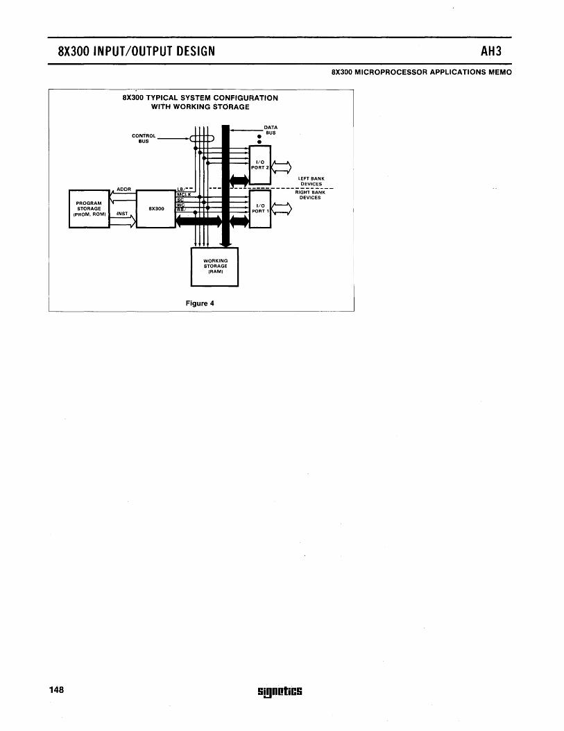
8X300 INPUT/OUTPUT DESIGN
PROGRAM STORAGE
(PROM. ROM)
148
8X300 TYPICAL SYSTEM CONFIGURATION WITH WORKING STORAGE
DATA I
BUS CONTROL ,.
~ • BUS ..... .....!-
1/0 H PORT 2
.L ~
.. ADDR LB;-- --- I.J __ !_~ ____
MCLK SI
'I W 1/0 ~ 8X300 RBI PORT 1 ...... INS~ .. .. .L ~
-V ,. T T ___
WORKING STORAGE
(RAM)
Figure 4
LEFT BANK DEVICES
RIGHT BANK DEVICES
S!,gnotics
AH3 8X300 MICROPROCESSOR APPLICATIONS MEMO
8X300 APPLICATIONS AH4 8X300 MICROPROCESSOR APPLICATIONS MEMO
FLOPPY DISC INTERFACE DESCRIPTION The 8X300 controls a floppy disc drive with a minimal amount of additional circuitry. In this example, byte assembly and disassembly are performed by the program ("bit banging") to reduce interface circuitry. Addition of such circuitry would increase hardware costs and decrease significantly peak processor utilization.
Data is transferred to and from the floppy disc via 1/0 driver routines. These 1/0 driver routines provide a standard software interface to a floppy disc and require 180 words of program storage. When not transferring data to and from the disc, the 8X300 is available to service other devices such as keyboards, displays or data communication lines. Figure 1 illustrates the system.
DESIGN APPROACH Data bytes are assembled or disassembled by sensing a clock, inputing data bit or generating clock, and outputing a data bit. Preamble patterns, track address, and other disc format requirements are implemented by programming. Disc drive head must be stepped to the desired track before data transfer is initiated. Disc drive status is monitored to determine any error conditions. A four step procedure is followed to implement the design:
1. Analyze interface. Analyze floppy disc relative to: Number of control/data lines, timing and data rates associated with each control/data line, and electrical characteristics of each control/data line. Determine any supplemental circuits needed for electrical compatibility (see Table 1).
2. Perform functional analysis. The functions to be programmed and any which require supplemental logic are determined. In this case, supplemental logic is utilized to process the 250ns pulses associated with DATA, CLOCK and WR DATA. Optional logic for byte assembly and disassembly also are shown. The programmed functions are: a. Byte assembly/disassembly b. Generate preamble, track address, timing
and sector synchronization c. Sense clock and disc status d. Step head to desired track
3. Define the program to process input and to generate output (see Figure 2).
4. Determine 8X300 configuration (see Table 2).
8X300
IV 8YTES
IV1
I I I I I I I
~----~
IV2
S!!IDotiCS
FLOPPY DISC INTERFACE
r--------, BYTE DISASSEMBLY 1---JVV'v"'"
OPTIONk-C - - - - -1-J LOGIC: r:~--71
~~O~~J
DATA
~f\A. ___ -o +5V __
CLOCK
WR PROTECT
Figure 1
FLOPPY DISC DRIVE
(MEMOREX 651)
149
8X300 APPLICATIONS
SIGNAL NAME
STEP IN STEP OUT LOAD HEAD UNSAFE RESET WR ENB WR DATA SECTOR INDEX TRKOO UNSAFE WR PROTECT DATA CLOCK
R = Resistor T = Transistor
FF = Flip-Flop
DATA RATE-1
20ms 20ms Level Level Level
2J..1s Sms
160ms Level Level Level 4J..1s 4J..1s
AH4
8X300 MICROPROCESSOR APPLICATIONS MEMO
SIGNAL ELECTRICAL #IV INTERFACE FUNCTION
DURATION CHARACTERISTICS BITS REQUIRED
.01-10ms TTL with pullup 1 Step head 1 track in
.01-10ms TTL with pullup 1 Step head 1 track out TTL with pullup 1 Load head TTL with pullup 1 Clears unsafe condition TTL with pullup 1 Enables write operation
.2SJ..1s SOmA current 1 2R,T Data/clock to disc 1ms OC output 1 R Sector indicated 1ms OC o!Jtput 1 R Begin of track indicator
OC output 1 R Head on track 00 OC output 1 R Unsafe condition indicator OC output 1 R Write protected disc
.2SJ..1s OC output 1 R,2FF Data from disc
.2SJ..1s OC output 1 R,FF Clock from disc
Table 1 INTERFACE ANALYSIS
FUNCTIONAL ANALYSIS
,----------------------I WR1 XEC DATBLE (R3) GET DATA BYTE
I XMIT 8. R1 INITIALIZE BIT COUNT
I WR2
I I I I I
MOVE
XMIT
ADD
NZT
JMP
MOVE
R2. DWRDAT WRITE DATA BIT
1. DWRDAT
R1. R1
R1. WR3
NXTWR BYTE DISASSEMBLED
ROTATE DATA BYTE I WR3 ----.... ~ ... ---------_ ..... R2(1). R2
150
CALL WAIT
WR4 XMIT O. DWRCLK CLOCK GENERATION
XMIT 1. DWRCLK
SEL DSTAT
NZT DINDEX. *+2
JMP TEND
SEL DCMMD
NO NZT R5. TENDL
JMP WR2
NXTWR ADD R3. R3 DECREMENT DATA POINTER
NZT R3. WRO
XMIT O. DWRCLK CLOCK GENERATION
XMIT 1. DWRCLK
XMIT 2. R3 RESET POINTER
JMP WR1
TEND XMIT 1. R5 SET SWITCH
NO SEL DCMMD
- - - - - - - - .., JMP WR2 I L ____________________ _
Through P!Jt: (a) Peak data rate: 2S0K bits/sec. (b) Peak processor utilization: 97.S%, including byte assembly/disassembly. (c) Peak processor utilization: 12.2%, with external byte assembly/disassembly.
Figure 2
ROM/PROM FOR WORKING STORAGE FOR IV BYTES FOR PROGRAM STORAGE DATA BUFFERS INPUT/OUTPUT INTERFACE
Input Driver ..................... 76 words 2S6 Bytes 6 IV bits for output Output Driver .................... 74 words 7 IV bits for input Head Step Driver ................ 30 words Total: 2 IV bytes
Total .......................... 180 words
Table 2 8X300 CONFIGURATION
Si!lDotiCS
8X300 APPLICATIONS AH4 8X300 MICROPROCESSOR APPLICATIONS MEMO
TELETYPE MULTIPLEXER DESCRIPTION The 8X300 is easily interfaced to a teletype or similar asynchronous device. Processor utilization is less than .1%, even when used in a character assembly mode.
A single 8X300 can be used as a multiplexer for many low speed asynchronous devices. For example, the 8X300 can be used as a front end multiplexer for a large computer system. Figure 3 illustrates the system.
DESIGN APPROACH A basic teletype I/O driver routine receives, transmits and echoes a character. Character assembly/disassembly is implemented by sensing start bit, sampling data bit and generating output bit timing. A four-step procedure is followed to implement the design:
1. Analyze interface. Analyze teletype relative to: Number of control/data lines, timing and data rates associated with each control/data line, electrical characteristics of each control/data line, and determine any supplemental circuits needed for electrical compatibility (see Table 3).
2. Perform functional analysis. The functions to be programmed and any which require supplemental logic are determined. In this case, no supplemental logic is required. The programmed functions are:
a. Character assembly/disassembly b. Sense start bit c. Generate bit timing and simultaneous char
acter echo 3. Define the program to process input and to
generate output (see Figure 4). 4. Determine 8X300 configuration (see Table 4).
8X300
SIG-NAL NAME
TTY OUT TTY IN
R = Resistor T = Transistor C = Capacitor
TELETYPE MULTIPLEXER
IV BYTES
IV 1
TTY OUT
TELETYPE
IV 2
TTY IN
ADDITIONA !V BYTES .... ___ TO/FROM COMPUTER INTERFACE
AS REQUIRED
Figure 3
SIGNAL ELECTRICAL INTER-DATA DURA- CHARACTER- #IV FACE RE-RATE TION ISTICS BITS au IRED FUNCTION
9.09ms 9.09ms 20mA current 1 3R,T Data to TTY printer 9.09ms 9.09ms 20mA current 1 4R,T,C Data from TTY keyboard
Table 3 INTERFACE ANALYSIS
!i!!l0otiC!i 151
8X300 APPLICATIONS AH4
152
8X300 MICROPROCESSOR APPLICATIONS MEMO
FUNCTIONAL ANALYSIS
r----------------------------------WAIT 4.Sms
OUTPUT START BIT
I I I DELAY1
I .-___ .... , _ _____ ..J
NO
------.., ~-...L...--..., I
I I I
XMIT
CALL
XMIT
MOVE
XOR
XMIT
XMIT
XOR
MOVE
ADD
NZT
XMIT
CALL
220.R1 WAIT 9 MSEC
DELAY
2.IVL SHIFT IN DATA BIT
TTYIN.AUX
RS.RS
1.IVL ECHO DATA BIT
1.AUX
RS.TTYOUT
RS(11.RS
R3.R3 BYTE ASSEMBLED?
R3.DELAY1
220.R1
DELAY
L _______ ~ ________________________ _
Through put: (a) Peak data rate: 220 bits/sec. (b) Peak Processor utilization: .05%
Figure 4
ROM/PROM FOR WORKING STORAGE FOR IV BYTES FOR PROGRAM STORAGE DATA BUFFERS INPUT/OUTPUT INTERFACE
Teletype driver ................... 49 words 2 bytes per Teletype 1 IV bit, for output, per Teletype Delay routine ..................... 10 words 1 IV bit for input, per Teletype
Total ........................... 59 words Total: 2 IV bytes per 8 Teletypes
Table 4 8X300 CONFIGURATION
SmDDliCS
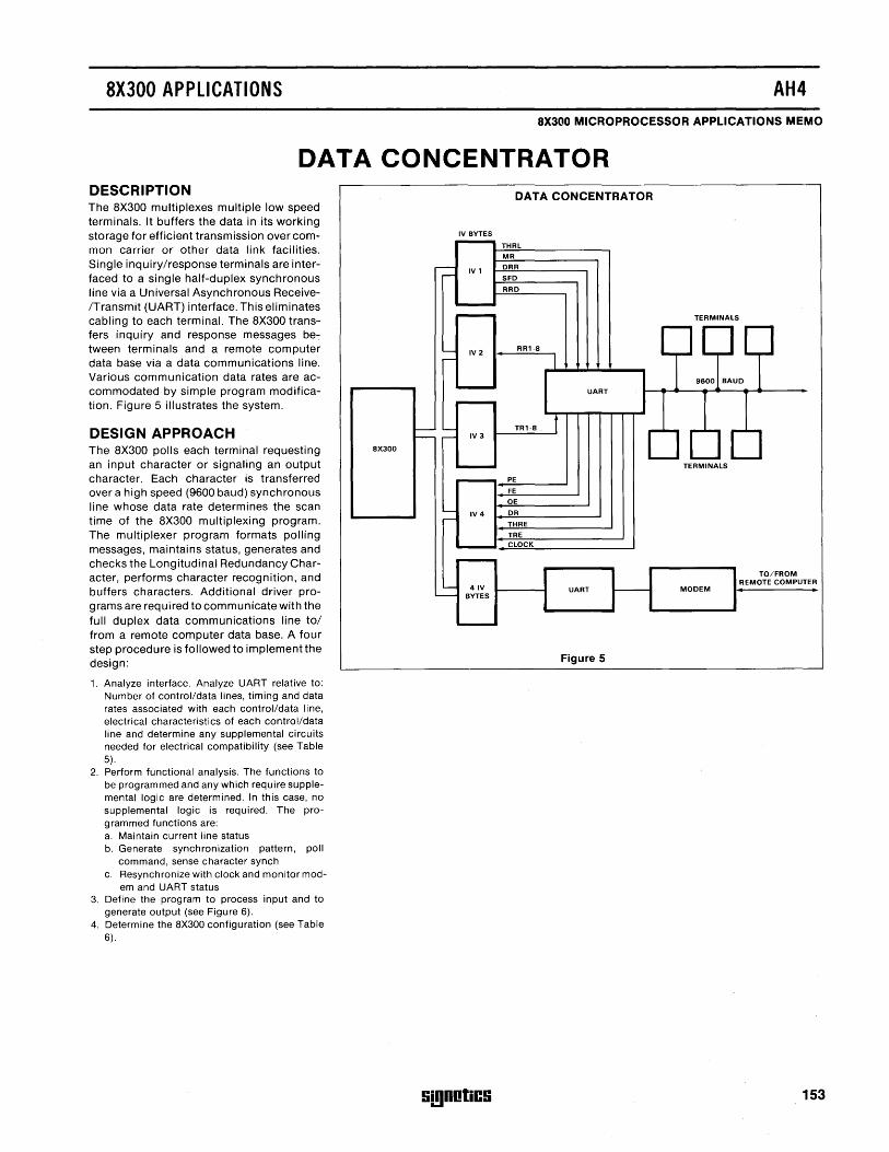
8X300 APPLICATIONS AH4 8X300 MICROPROCESSOR APPLICATIONS MEMO
DATA CONCENTRATOR DESCRIPTION The 8X300 multiplexes multiple low speed terminals. It buffers the data in its working storage for efficient transmission over common carrier or other data link facilities. Single inquiry/response terminals are interfaced to a single half-duplex synchronous line via a Universal Asynchronous Receive/Transmit (UART) interface. This eliminates cabling to each terminal. The 8X300 transfers inquiry and response messages between terminals and a remote computer data base via a data communications line. Various communication data rates are accommodated by simple program modification. Figure 5 illustrates the system.
DESIGN APPROACH The 8X300 polls each terminal requesting an input character or signaling an output character. Each character is transferred over a high speed (9600 baud) synchronous line whose data rate determines the scan time of the 8X300 multiplexing program. The multiplexer program formats polling messages, maintains status, generates and checks the Longitudinal Redundancy Character, performs character recognition, and buffers characters. Additional driver programs are required to communicate with the full duplex data communications line to/ from a remote computer data base. A four step procedure is followed to implement the design:
1. Analyze interface. Analyze UART relative to: Number of control/data lines, timing and data rates associated with each control/data line, electrical characteristics of each control/data line and determine any supplemental circuits needed for electrical compatibility (see Table 5).
2. Perform functional analysis. The functions to be programmed and any which require supplemental logic are determined. In this case, no supplemental logic is required. The programmed functions are: a. Maintain current line status b. Generate synchronization pattern, poll
command, sense character synch c. Resynchronize with clock and monitor mod
em and UART status 3. Define the program to process input and to
generate output (see Figure 6). 4. Determine the 8X300 configuration (see Table
6).
DATA CONCENTRATOR
IV BYTES
UART
8X300
Figure 5
Si!lDOliCS
TERMINALS
TERMINALS
MODEM
TO/FROM REMOTE COMPUTER
153
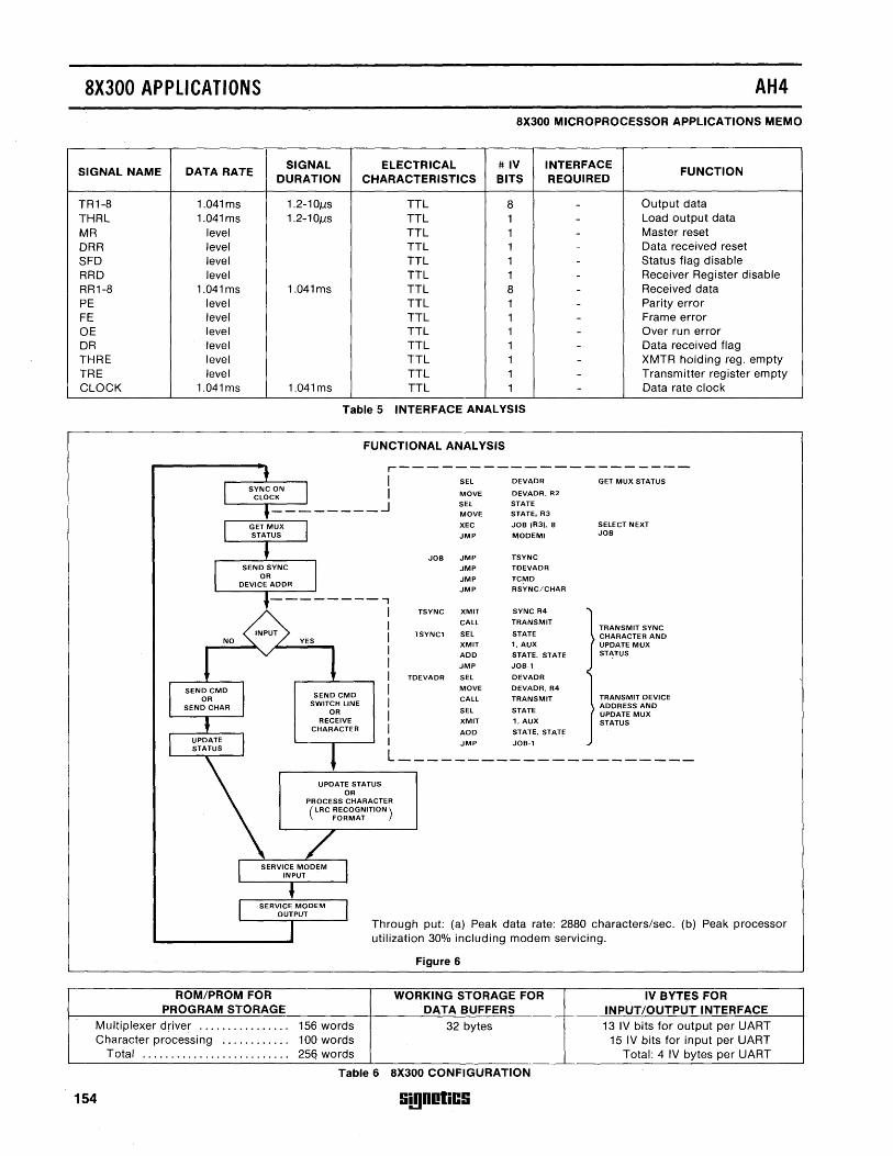
8X300 APPLICATIONS AH4
SIGNAL NAME
TR1-8 THRL MR ORR SFD RRD RR1-8 PE FE OE DR THRE TRE CLOCK
8X300 MICROPROCESSOR APPLICATIONS MEMO
SIGNAL ELECTRICAL #IV INTERFACE DATA RATE
DURATION CHARACTERISTICS BITS REQUIRED FUNCTION
1.041 ms 1.2-10/.1s TTL 8 1.041 ms 1.2-10/.1s TTL 1
level TTL 1 level TTL 1 level TTL 1 level TTL 1
1.041 ms 1.041ms TTL 8 level TTL 1 level TTL 1 level TTL 1 level TTL 1 level TTL 1 level TTL 1
1.041 ms 1.041 ms TTL 1
Table 5 INTERFACE ANALYSIS
FUNCTIONAL ANALYSIS
SEL DEVADR
MOVE DEVADR.R2
SEL STATE
MOVE STATE, R3
XEC JOB (R3). 8
JMP MODEMI
JOB JMP TSYNC
JMP TDEVADR
JMP TCMD
JMP RSYNC/CHAR
----
----------
Output data Load output data Master reset Data received reset Status flag disable Receiver Register disable Received data Parity error Frame error Over run error Data received flag XMTR holding reg. empty Transmitter register empty Data rate clock
GET MUX STATUS
SELECT NEXT JOB
--------,
ROM/PROM FOR PROGRAM STORAGE
I I I I I
TSYNC
TSYNC1
XMIT
CAll
SEL
XMIT
ADD
JMP
I TDEVADR SEL
I I I I I
MOVE
CALL
SEL
XMIT
ADD
JMP
SYNC R4
TRANSMIT
STATE
1. AUX
STATE. STATE
JOB·1
DEVADR
DEVADR. R4
TRANSMIT
STATE
1. AUX
STATE. STATE
JOB·1
1 TRANSMIT SYNC CHARACTER AND UPDATE MUX STATUS
1 TRANSMIT DEVICE ADDRESS AND UPDATE MUX STATUS
L ____________________ _
UPDATE STATUS OR
PROCESS CHARACTER
( LRC RECOGNITION)
FORMAT
Through put: (a) Peak data rate: 2880 characters/sec. (b) Peak processor utilization 30% including modem servicing.
Figure 6
WORKING STORAGE FOR IV BYTES FOR DATA BUFFERS INPUT/OUTPUT INTERFACE
Multiplexer driver ................ 156 words 32 bytes 13 IV bits for output per UART Character processing '" ......... 100 words 15 IV bits for input per UART
Total .......................... 25q words Total: 4 IV bytes per UART
Tallie 6 8X300 CONFIGURATION
154 S!!)DotiCS
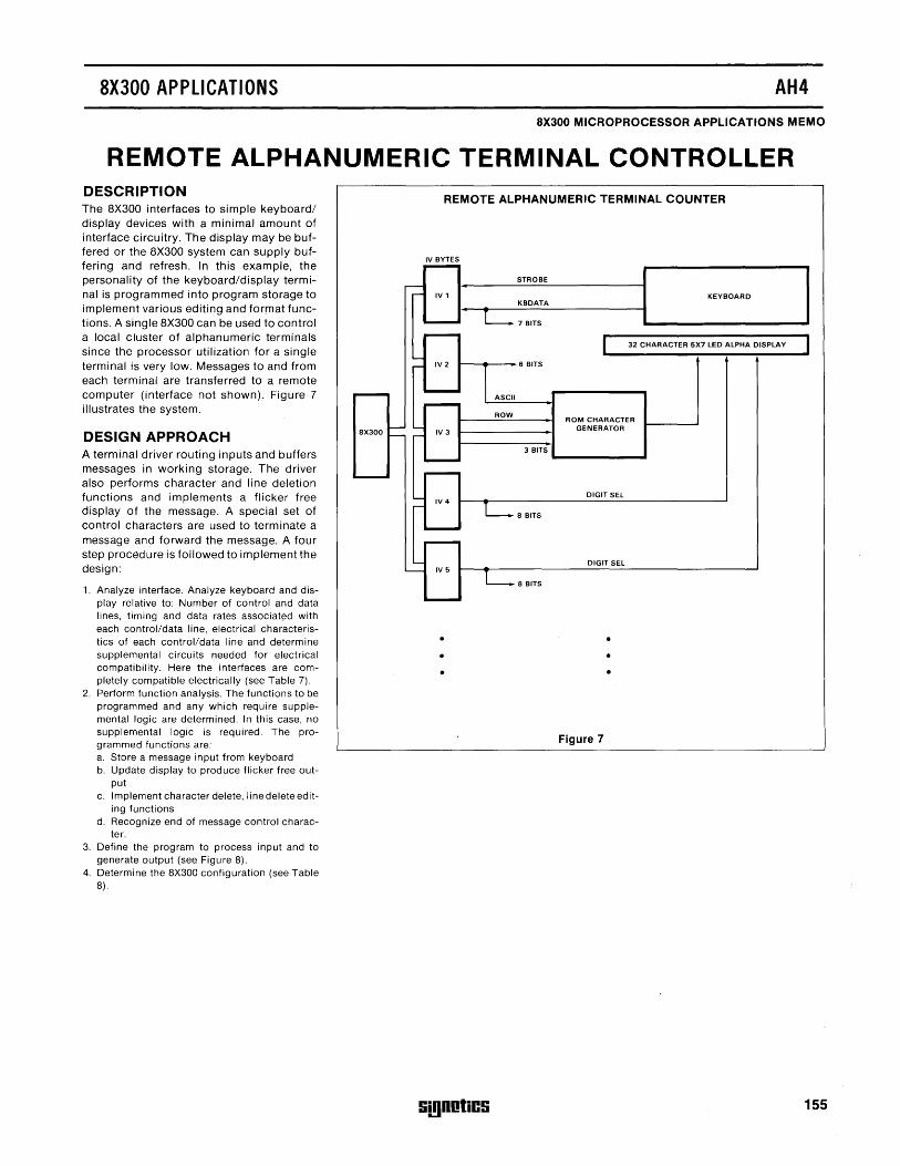
8X300 APPLICATIONS AH4
8X300 MICROPROCESSOR APPLICATIONS MEMO
REMOTE ALPHANUMERIC TERMINAL CONTROLLER DESCRIPTION The 8X300 interfaces to simple keyboard/ display devices with a minimal amount of interface circuitry. The display may be buffered or the 8X300 system can supply buffering and refresh. In this example, the personality of the keyboard/display terminal is programmed into program storage to implement various editing and format functions. A single 8X300 can be used to control a local cluster of alphanumeric terminals since the processor utilization for a single terminal is very low. Messages to and from each terminal are transferred to a remote computer (interface not shown). Figure 7 illustrates the system.
DESIGN APPROACH A terminal driver routing inputs and buffers messages in working storage. The driver also performs character and line deletion functions and implements a flicker free display of the message. A special set of control characters are used to terminate a message and forward the message. A four step procedure is followed to implement the design:
1. Analyze interface. Analyze keyboard and display relative to: Number of control and data lines, timing and data rates associated with each control/data line, electrical characteristics of each control/data line and determine supplemental circuits needed for electrical compatibility. Here the interfaces are completely compatible electrically (see Table 7).
2. Perform function analysis. The functions to be programmed and any which require supplemental logic are determined. In this case, no supplemental logic is required. The programmed functions are: a. Store a message input from keyboard b. Update display to produce flicker free out
put c. Implement character delete, line delete edit
ing functions d. Recognize end of message control charac
ter. 3. Define the program to process input and to
generate output (see Figure 8). 4. Determine the 8X300 configuration (see Table
8).
8X300
REMOTE ALPHANUMERIC TERMINAL COUNTER
IV BYTES
STROBE
KBDATA
7 BITS
1--_>--__ 6 BITS
3 BITS
8 BITS
8 BITS
S!!IDotiCS
KEYBOARD
32 CHARACTER 5X7 LED ALPHA DISPLAY
ROM CHARACTER GENERATOR
.... ----_ .. DIGIT SEL
DIGIT SEL
•
Figure 7
155
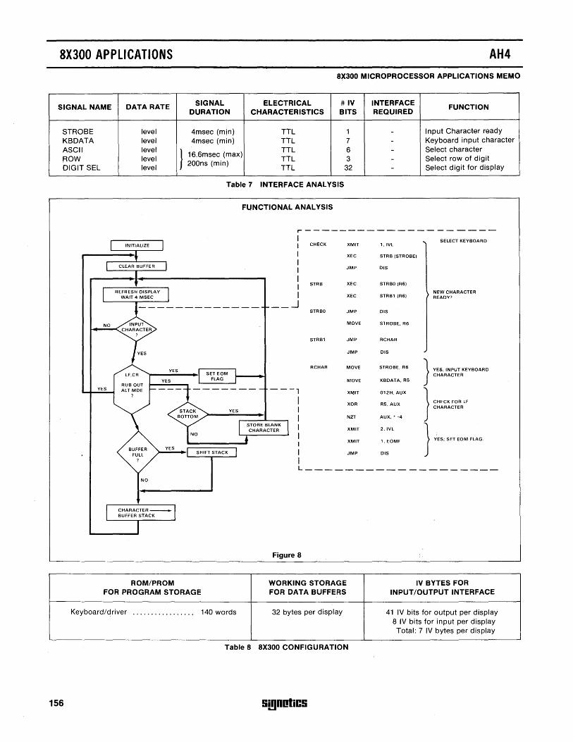
8X300 APPLICATIONS AH4
8~300 MICROPROCESSOR APPLICATIONS MEMO
SIGNAL NAME DATA RATE SIGNAL ELECTRICAL #IV INTERFACE FUNCTION DURATION CHARACTERISTICS BITS REQUIRED
STROBE level 4msec (mjn) TTL 1 - Input Character ready KBDATA level 4msec (min) TTL 7 - Keyboard input character ASCII level
} 16.6msec (max) TTL 6 - Select character
ROW level TTL 3 - Select row of digit DIGIT SEL level
200ns (min) TTL 32 - Select digit for display
Table 7 INTERFACE ANALYSIS
FUNCTIONAL ANALYSIS
r- -------------- -- ----
I SELECT KEYBOARD I CHECK XMIT 1,IVL
I XEC STRB (STROBE)
I I JMP DIS
I I STRB XEC STRBO (R6)
I NEW CHARACTER XEC STRB1 (R6) READY?
__ -.J STRBO JMP DIS
MOVE STROBE, R6
STRB1 JMP RCHAR
JMP DIS
RCHAR MOVE STROBE, R6 } m, 'N,"",,"O,"O YES CHARACTER
YES MOVE KBDATA,R5 RUB OUT
YES ALT MOE ---, XMIT 012H, AUX
I XOR R5, AUX } '""",0",' I CHARACTER
I NZT AUX,' +4
I XMIT 2,IVL
} Y,", '" >OM RAG I I XMIT 1, EOMF
I JMP DIS
I L ___________________
Figure 8
ROM/PROM WORKING STORAGE IV BYTES FOR FOR PROGRAM STORAGE FOR DATA BUFFERS INPUT/OUTPUT INTERFACE
Keyboard/driver ................. 140 words 32 bytes per display 41 IV bits for output per display 8 IV bits for input per display Total: 7 IV bytes per display
Table 8 8X300 CONFIGURATION
156 Si!]DotiCS
8X300 APPLICATIONS AH4
8X300 MICROPROCESSOR APPLICATIONS MEMO
COMPUTER I/O BUS EMULATOR DESCRIPTION The 8X300 system emulates a Microdata 1600 I/O bus. Microdata I/O bus compatible peripherals may then be easily connected to and controlled by a standard 8X300 system. A Microdata I/O bus driver program provides a standard software interface to peripheral devices and requires only 27 words of program storage. Figure 9 illustrates the system.
DESIGN APPROACH Data bytes are transferred to and from the I/O bus in accordance with Microdata I/O bus specifications. Control signal timing and data transfer sequences are generated by programming. A four step procedure is followed to implement the design:
1. Analyze interface. Analyze Microdata I/O bus relative to: Number of control/data lines, timing and data rates associated with each control/data line, electrical characteristics of each control/data line and determine supplemental circuits needed for electrical compatibility (see Table 9).
2. Perform functional analysis. The functions to be programmed and any which require supplemental logic are determined. In this case, no supplemental logic is required. The programmed functions are: a. Transfer bytes in and out b. Generate control signal timing and data
transfer sequences 3. Define the program to process input and to
generate output (see Figu re 10). 4. Determine the 8X300 configuration (see Table
10).
-8X300 -
COMPUTER I/O BUS EMULATOR
IV BYTES
DATA 0 ----r-- IV 1 110 BUS y DRIVERS
I T BIC
+5V BOC
~
RESISTOR ... DATA I - IV 2 TERMINATION r--
""
I T BOC +5V
BIC
~
L....- IV 3 DRIVERS L.---
I I BIC
+5V
BOC
l
Figure 9
S!!IDotiCS
0000
0001
0002
0003
0004
0005
0006
0007
1000
1001
1002
1003
1004
1005
1006
1007
COXX
OIXX
OOXX
MICROOATA 1600
1/0 BUS
157
8X300 APPLICATIONS AH4
8X300 MICROPROCESSOR APPLICATIONS MEMO
SIGNAL NAME DATA RATE SIGNAL ELECTRICAL #IV INTERFACE
FUNCTION DURATION CHARACTERISTICS BITS REQUIRED
ODOO-07 level open collector 8 8D Data/address from computer IDOO-07 level TTL 8 8R Data to computer COXX 4J1s 1.25J1s open collector 1 D Control output timing DIXX 4J1s 1.25J1s open collector 1 D Data input timing DOXX 4J1s .75-1.25J1s open collector 1 D Data output timing
D = Open collector driver R = Resistors
Table 9 INTERFACE ANALYSIS
FUNCTIONAL ANALYSIS
MICROIO XMIT 1.IVL
MOVE R1. DATAO
XMIT 3.IVL
XMIT 1. COXX PULSE ON
XEC TAB (R3)
NOP
NOP
XMIT O.COXX PULSE OFF
MOVE R2.IVR
NZT R3 •. INPUT
OUTPUT MOVE WS. DATAO
ADDRESS OUTPUT BUFFER DATA
MEMORY BYTE
NOP
DELAY BETWEEN DATA XMIT 3.IVL
AND DOXX PULSE
XMIT 1. DOXX PULSE ON
NOP GENERATE GENERATE
NOP 1.2118 1.251'5 PULSE DOXX PULSE NOP
XMIT O. DOXX PULSE OFF
TAB XMIT 1.IVL
XMIT 2.IVL
Figure 10
-ROM/PROM FOR WORKING STORAGE IV BYES FOR
PROGRAM STORAGE FOR DATA BUFFERS INPUT/OUTPUT INTERFACE
I/O Driver ....................... 27 words Depends on peripheral 11 IV bits for output 8 IV bits for input
Total: 3 IV bytes per peripheral
Table 10 8X300 CONFIGURATION
158 S!!IDotiCS
8X300 APPLICATIONS AH4
8X300 MICROPROCESSOR APPLICATIONS MEMO
INTERFACE TO EXTERNAL READ/WRITE MEMORY DESCRIPTION The 8X300 controls the storage, retrieval and processing of large blocks of data. Data is stored in a large capacity (up to 64K bytes) read/write RAM external to the 8X300 system. The memory is assembled from widely available n-channel (n-MOS) static or dynamic RAM circuits. Minimal interface circuitry is required to connect the 8X300 Interface Vector bytes to the address, data and control lines of the external memory. Figure 11 illustrates the system.
DESIGN APPROACH Data bytes are read from or written into memory through a single IV type. Two additional IV bytes are used as a 16-bit address reg ister to the external memory. 16 bits provide an address range of 65K bytes. The read/write control signals to the memory require two IV bits. Instruction sequences are used for memory read and memory write operations to implement 1 to 2 microsecond memory access times. A four step procedure is followed to implement the design:
1. Analyze interface. Analyze n-MOS RAM circuits relative to: Number of control/data lines, timing and data rates associated with each control/data line, electrical characteristics of each control/data line and determine any supplemental circuits needed for electrical compatibility (see Table 11).
2. Perform functional analysis. The functions to be programmed and any which require supplemental logic are determined. The programmed functions are: a. Store memory address in IV bytes ADRHI,
ADRLO. b. Set appropriate read/write control bits c. Wait for memory operation complete
3. Define the program to process input and to generate output. a. GET instruction sequence to read memory
location addressed by contents of IV bytes ADRHI, ADRLO (see Figure 12).
b. PUT instruction sequence to write data into the memory location addressed by the contents of IV bytes ADRH I, ADRLO (see Figure 13).
4. Determine the 8X300 configuration (see Table 12).
INTERFACE TO EXTERNAL READ/WRITE MEMORY
IV BYTES
ADRHI
8 BITS
!i!!ln~tiC!i
EXTERNAL MEMORY (UP TO 65K BYTES)
ADDRESS/CHIP SELECT
r----------, I
I I I I I I I I
DATAIN ~
DATA OUT;
I I I I I
NMOS RAM ARRAY
READ/WRITE CONTROL I L __________ ..1
Figure 11
159
8X300 APPLICATIONS AH4
8X300 MICROPROCESSOR APPLICATIONS MEMO
SIGNAL NAME DATA RATE SIGNAL ELECTRICAL # IV INTERFACE
FUNCTION DURATION CHARACTERISTICS BITS REQUIRED
ADRHI Level TTL 8 * Most significant none byte, Memory
address, and chip select input
ADRLO Level TTL 8 * Least significant none byte memory
address
DATA Level TTL 8 * Memory data none
R/W 500ns (min) >250ns TTL 1 * Memory read/write
none control
R/W DELAY 500ns (min) >500ns TTL 1 * Data enable delay
none during memory write
Table 11 INTERFACE ANALYSIS
GET INSTRUCTION SEQUENCE
l STORE MEMORY XMIT ADRHI. IVL
ADDRESS MOVE "ADDRESS Hr', ADRHI 1 ADD"",,"' XMIT ADRLO, IVL MEMORY
MOVE "ADDRESS LOW", ADRLO I' ---------------------------------
GET XMIT CNTRL, IVL SET READ CONTROL
BIT XMIT 5, CNTRL } 'CAD DATA
XMIT 7, CNTRL
1.0,,5 < XMIT DATA, IVL
,...-----------------------/ ..,
/ /
DELAY 250NS / /
/ ) DATA AVAILABLE /
/ • FOR PROCESSING .. ____ J
• READ DATA BYTE •
l Figure 12
160 Si!lDOtiCS
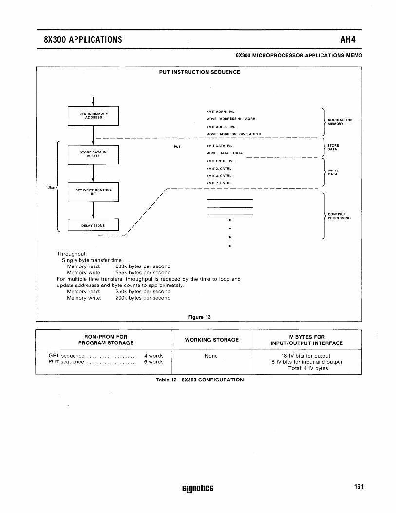
8X300 APPLICATIONS AH4
8X300 MICROPROCESSOR APPLICATIONS MEMO
STORE MEMORY ADDRESS
STORE DATA IN IV BYTE
PUT INSTRUCTION SEQUENCE
XMIT ADRHI. IVl
MOVE "ADDRESS HI", ADRHI
XMIT ADRlO, IVl
MOVE "ADDRESS lOW", ADRlO
PUT XMIT DATA, IVl
MOVE "DATA", DATA
XMIT CNTRl, IVl
XMIT 2, CNTRl
XMIT 3, CNTRl
XMIT 7, CNTRl
1 ADDRESS THE MEMORY
}
STORE DATA
1 WRITE DATA
1.5/15 ( SET WRITE CONTROL
BIT r-----------------------
DELAY 250NS
/ ____ .J
Throughput: Single byte transfer time
/ /
/
/ /
/ /
/
Memory read: 833k bytes per second Memory write: 555k bytes per second
• • • •
For multiple time transfers, throughput is reduced by the time to loop and update addresses and byte counts to approximately:
Memory read: 250k bytes per second Memory write: 200k bytes per second
Figure 13
ROM/PROM FOR WORKING STORAGE
PROGRAM STORAGE
GET sequence .................... 4 words None PUT sequence .................... 6 words
Table 12 8X300 CONFIGURATION
G!!IDotiCG
IV BYTES FOR INPUT/OUTPUT INTERFACE
18 IV bits for output 8 IV bits for input and output
Total: 4 IV bytes
161
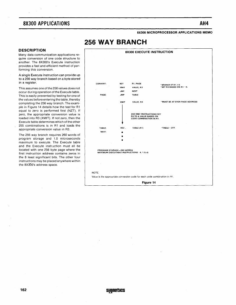
8X300 APPLICATIONS
DESCRIPTION Many data communication applications require conversion of one code structure to another. The 8X300's Execute instruction provides a fast and efficient method of performing this conversion.
A single Execute instruction can provide up to a 256 way branch based on a byte stored in a register.
This assumes one of the 256 values does not occur during operation of the Execute table. This is easily prevented by testing for one of the values before entering the table, thereby completing the 256 way branch. The example in Figure 14 details how the test for R1 equal to zero is performed first (NZT). If zero, the appropriate conversion value is loaded into R3 (XMIT). If not zero, then the Execute table determines which of the other 255 combinations is in R1 and loads the appropriate conversion value in R3.
The 256 way branch requires 260 words of program storage and 1.0 microseconds maximum to execute. The Execute table and the Execute instruction must all be located with one 256 byte page where the first instruction address contains zeros in the 8 least Significant bits. The other four instructions may be placed anywhere within the 8X3t)0's address space.
162
AH4
8X300 MICROPROCESSOR APPLICATIONS MEMO
256 WAY BRANCH
CONVERT:
PAGE:
TABLE:
NEXT:
8X300 EXECUTE INSTRUCTION
NZT
XMIT
JMP
JMP
XMIT
I XEC.
• • •
R1. PAGE
VALUE. R3
NEXT
TABLE
VALUE. R3
"BRANCH IF R1 to. "SET R3 BASED ON R1 0 O.
"MUST BE AT EVEN PAGE ADDRESS
255 XMIT INSTRUCTIONS SET R3 TO A VALUE BASED ON CODE COMBINATION IN R1.
TABLE (R1) "TABLE 0377.
PROGRAM STORAGE-260 WORDS MAXIMUM EXECUTABLE INSTRUCTIONS-4; 1.01'5
NOTE
Value is the appropriate conversion code for each code combination in R1.
Figure 14
S!!IDOliCS
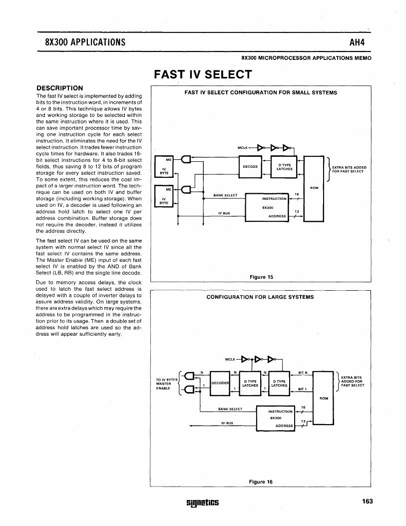
8X300 APPLICATIONS
DESCRIPTION The fast IV select is implemented by adding bits to the instruction word, in increments of 4 or a bits. This technique allows IV bytes and working storage to be selected within the same instruction where it is used. This can save important processor time by saving one instruction cycle for each select instruction. It eliminates the need for the IV select instruction. It trades fewer instruction cycle times for hardware. It also trades 16-bit select instructions for 4 to a-bit select fields, thus saving a to 12 bits· of program storage for every select instruction saved. To some extent, this reduces the cost impact of a larger instruction word. The technique can be used on both IV and buffer storage (including working storage). When used on IV, a decoder is used following an address hold latch to select one IV per address combination. Buffer storage does not require the decoder, instead it utilizes the address directly.
The fast select IV can be used on the same system with normal select IV since all the fast select IV contains the same address. The Master Enable (ME) input of each fast select IV is enabled by the AND of Bank Select (LB, RB) and the single line decode.
Due to memory access delays, the clock used to latch the fast select address is delayed with a couple of inverter delays to assure address validity. On large systems, there are extra delays which may require the address to be programmed in the instruction prior to its usage. Then a double set of address hold latches are used so the address will appear sufficiently early.
AH4
8X300 MICROPROCESSOR APPLICATIONS MEMO
FAST IV SELECT FAST IV SELECT CONFIGURATION FOR SMALL SYSTEMS
ROM
IV BUS
Figure 15
CONFIGURATION FOR LARGE SYSTEMS
BANK SELECT
IV BUS
Si!lDotiCS
BIT N
BIT 1
16 INSTRUCTION 1---1---1
8X300
Figure 16
}
EXTRA BITS ADDED FOR FAST SELECT
ROM
}
EXTRA BITS ADDED FOR FAST SELECT
163
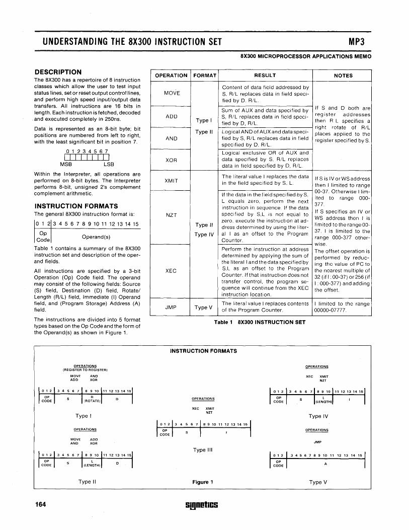
UNDERSTANDING THE 8X300 INSTRUCTION SET MP3
DESCRIPTION The 8X300 has a repertoire of 8 instruction classes which allow the user to test input status lines, set or reset output control lines, and perform high speed input/output data transfers. All instructions are 16 bits in length. Each instruction is fetched, decoded
,and executed completely in 250ns.
Data is represented as an 8-bit byte; bit positions are numbered from left to right, with the least Significant bit in position 7.
o 1 2 3 4 5 6 7 I I I I I I I I I
MSB LSB
Within the Interpreter, all operations are performed on 8-bit bytes. The Interpreter performs 8-bit, unsigned 2's complement complement arithmetic.
INSTRUCTION FORMATS The general 8X300 instruction format is:
o 1 2 3 4 5 6 7 8 9 10 11 12 13 14 15
Op Code
Operand(s)
Table 1 contains a summary of the 8X300 instruction set and description of the operand fields.
All instructions are specified by a 3-bit Operation (Op) Code field. The operand may consist of the following fields: Source (S) field, Destination (D) field, Rotatel Length (R/L) field, Immediate (I) Operand field, and (Program Storage) Address (A) field.
The instructions are divided into 5 format types based on the Op Code and the form of the Operand(s) as shown in Figure 1.
164
OPERATIONS (REGISTER TO REGISTER)
MOVE ADD
AND XOR
Type I
OPERATIONS
MOVE ADD AND XOR
Type II
OPERATION
MOVE
ADD
AND
XOR
XMIT
NZT
XEC
JMP
FORMAT
Type I
Type II
Type II
Type IV
Type V
8X300 MICROPROCESSOR APPLICATIONS MEMO
RESULT
Content of data field addressed by S, R/L replaces data in field specified by 0, R/L.
NOTES
1----------------.., If Sand 0 both are Sum of AUX and data specified by S, R/L replaces data in field speci- register addresses fied by 0, R/L. then R L specifies a
1---------------...., right rotate of R/L Logical AND of AUX and data speci- places applied to the fied by S, R/L replaces data in field register specified by S. specified by 0, R/L.
Logical exclusive OR of AUX and data specified by S, R/L replaces data in field specified by 0, R/L.
The literal value I replaces the data in the field specified by S, L.
If S is IV or WS address then I limited to range
!----------------j 00-37. Otherwise Ilim-If the data in the field specified by S, ited to range 000-L equals zero, perform the next 377. instruction in sequence. If the data
If S specifies an IV or specified by S,L is not equal to WS address then I is zero, execute the instruction at ad-
limited totherangeOOdress determined by using the liter- 37. I is limited to the al I as an offset to the Program Counter. range 000-377 other-
I----------------j wise. Perform the instruction at address The offset operation is determined by applying the sum of performed by reducthe literal I and the data specified by ing the value of PC to S,L as an offset to the Program the nearest multiple of Counter. If that instruction does not 32 (if I: 00-37) or 256 (if transfer control, the program se- I: 000-377) and adding quence will continue from the XEC the offset. instruction location.
The literal value I replaces contents of the Program Counter.
I limited to the range 00000-07777 .
Table 1 8X300 INSTRUCTION SET
INSTRUCTION FORMATS
OPERATIONS
XEC XMIT NZT
OPERATIONS
XEC XMIT NZT
Type IV
8 9 10 11 12 13 1415
OPERATIONS
JMP
Type III 3 4 5 6 7 8 9 10 11 12 13 14 15
A
Figure 1 Type V
G!!IDOliCG
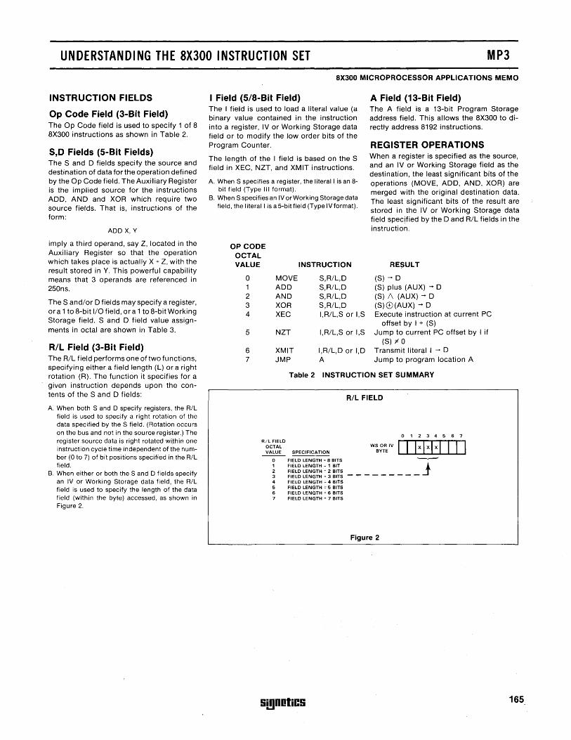
UNDERSTANDING THE 8X300 INSTRUCTION SET MP3
INSTRUCTION FIELDS
Op Code Field (3-Bit Field) The Op Code field is used to specify 1 of 8 8X300 instructions as shown in Table 2.
S,D Fields (S-Bit Fields) The Sand D fields specify the source and destination of data forthe operation defined by the Op Code field. The Auxiliary Register is the implied source for the instructions ADD, AND and XOR which require two source fields. That is, instructions of the form:
ADD X, Y
imply a third operand, say Z, located in the Auxiliary Register so that the operation which takes place is actually X + Z, with the result stored in Y. This powerful capability means that 3 operands are referenced in 250ns.
The S andlor D fields may specify a register, or a 1 to 8-bit 1/0 field, or a 1 to 8-bit Working Storage field. Sand D field value assignments in octal are shown in Table 3.
RIL Field (3-Bit Field) The R/L field performs one of two fu nctions, specifying either a field length (L) or a right rotation (R). The function it specifies for a given instruction depends upon the contents of the Sand D fields:
A. When both Sand D specify registers, the R/L field is used to specify a right rotation of the data specified by the S field. (Rotation occurs on the bus and not in the source register.) The register source data is right rotated within one instruction cycle time independent of the number (0 to 7) of bit positions specified in the R/L field.
B. When either or both the Sand D fields specify an IV or Working Storage data field, the R/L field is used to specify the length of the data field (within the byte) accessed, as shown in Figure 2.
aX300 MICROPROCESSOR APPLICATIONS MEMO
I Field (SIS-Bit Field) The I field is used to load a literal value (a binary value contained in the instruction into a register, IV or Working Storage data field or to modify the low order bits of the Program Counter.
The length of the I field is based on the S field in XEC, NZT, and XMIT instructions.
A. When S specifies a register, the literal I is an 8-bit field (Type III format).
B. When S specifies an IVorWorking Storage data field, the literal I is a 5-bit field (Type IV format).
OP CODE OCTAL VALUE INSTRUCTION
0 MOVE S,R/L,D 1 ADD S,R/L,D 2 AND S,R/L,D 3 XOR S,R/L,D 4 XEC I,R/L,S or I,S
5 NZT I,R/L,S or I,S
6 XMIT I,R/L,D or I,D 7 JMP A
A Field (13-Bit Field) The A field is a 13-bit Program Storage address field. This allows the 8X300 to directly address 8192 instructions.
REGISTER OPERATIONS When a register is specified as the source, and an IV or Working Storage field as the destination, the least significant bits of the operations (MOVE, ADD, AND, XOR) are merged with the original destination data. The least significant bits of the result are stored in the IV or Working Storage data field specified by the D and R/L fields in the instruction.
RE$ULT
(S) - D (S) plus (AUX) - D (S) 1\ (AUX) - D (S) 0 (AUX) - D Execute instruction at current PC
offset by I + (S) Jump to current PC offset by I if
(S) ~ 0 Transmit li.teral I - D Jump to program location A
Table 2 INSTRUCTION SET SUMMARY
R/L FIELD OCTAL VALUE
o 1 2 3 4 5 6 7
RIL FIELD
01234567
SPECIFICATION
FIELD LENGTH 8 BITS --j FIELD LENGTH 1 BIT FIELD LENGTH 2 BITS FIELD LENGTH 3 BITS - ..... - - - - - - -FIELD LENGTH 4 BITS FIELD LENGTH 5 BITS FIELD LENGTH 6 BITS FIELD LENGTH 7 BITS
Figure 2
S!!IDotiCS 16S
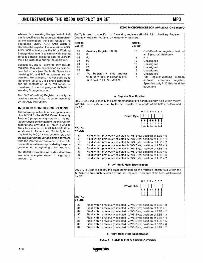
UNDERSTANDING THE 8X300 INSTRUCTION SET MP3
When an IV or Working Storage field of 1 to 8 bits is specified as the source, and a register as the destination, the 8-bit result of the operations (MOVE, ADD, AND, XOR) is stored in the register. The operations ADD, AND, XOR qctually use the IV or Working Storage data field (1 to 8 bits) with leading zeros to obtain 8-bit source data for use with the 8-bit AUX data during the operation.
Because IVL and IVR are write-only pseudo registers, they can be specified as destination fields only (see Table 3). Operations involving IVL and IVR as sources are not possible. For example, it is not possible to increment IVR or IVL in a single instruction, and the contents of IVL or IVR cannot be transferred to a working register, IV byte, or Working Storage location.
The OVF (Overflow) Register can only be used as a source field; it is set or reset only by the ADD instruction.
INSTRUCTION DESCRIPTIONS The following instruction descriptions employ MCCAP (the 8X300 Cross Assembly Program) programming notation. This notation varies somewhat from the instruction descriptions provided in Tables 1 and 3. Thus, for example, explicit L field definition, as shown in Table 1 and Table 3, is not required by MCCAP instructions; MCCAP creates appropriate variable field addresses from the information contained in the Data Declaration statements provided by the programmer at the beginning of his program.
The 8X300 instruction set is described below with examples shown in Figures 3 through 10.
166
8X300 MICROPROCESSOR APPLICATIONS MEMO
08-17 8 is used to specify 1 of 7 working registers (R1-R6, R11), Auxiliary Register, Overflow Register, IVL and IVR write-only registers.
OCTAL VALUE
00 01 02 03 04 05 06 07
Auxiliary Register (AUX) R1 R2 R3 R4 R5 R6 IVL Register-IV Byte address write-only register-Specified only in D field in all instructions
OCTAL VALUE
10
11 12 13 14 15 16 17
OVF-Overflow register-Used as an S (source) field only. R11 Unassigned Unassigned Unassigned Unassigned Unassigned IVR Register-Working Storage address write-only registerSpecified only in D field in all instructions
a. R~gister Specification
20-8-278 is used to specify the least significant bit of a variable length field within the IVI WS Byte previously selected by the IVL register. The length of the field is determined by R/L.
OCTAL VALUE
20 21 22 23 24 25 26 27
o 1 2 345 6 7
IV/WS Byte I I I I I I I I I ffftftff I I I I I I I I I I I I I I I I
Field within previously selected IV/WS Byte; position of LSB = 0 Field within previously selected IV/WS Byte; position of LSB = 1 Field within previously selected IV/WS Byte; position of LSB = 2 Field within previously selected IV/WS Byte; position of LSB = 3 Field within previously selected IV/WS Byte; position of LSB = 4 Field within previously selected IV/WS Byte; position of LSB = 5 Field within previously selected IV/WS Byte; position of LSB = 6 Field within previously selected IV/WS Byte; position of LSB = 7
b. Left Bank Field Specification
308-378 is used to specify the least Significant bit of a variable length field within the IV/WS Byte previously selected by the IVR Register. The length of the field is determined by R/L.
OCTAL VALUE
o 1 2 3 4 5 6 7
IV/WS Byte I I I I I I I I I f ••• fff. I I I I I I I I , I , I I , I ,
30 Field within previously selected IV/WS Byte; position of LSB = 0 31 Field within previously selected IV/WS Byte; position of LSB = 1 32 Field within previously selected IV/WS Byte; position of LSB = 2 33 Field within previously selected IV/WS Byte; position of LSB = 3 34 Field within previously selected IV/WS Byte; position of LSB = 4 35 Field within previously selected IV/WS Byte; position of LSB = 5 36 Field within previously selected IV/WS Byte; position of LSB = 6 37 Field within previously selected IV/WS Byte; position of LSB = 7
c. Right Bank Fi~ld Specification
Table 3 SAND D FIELD SPECIFICATIONS
Si!JDDtiCS
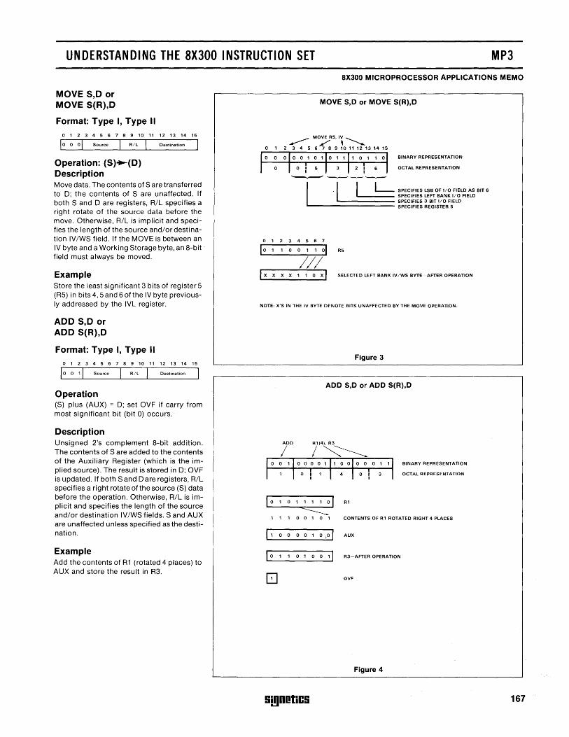
UNDERSTANDING THE 8X300 INSTRUCTION SET MP3
MOVE S,D or MOVE S(R),D
Format: Type I, Type II o 1 2 3 4 5 6 7 B 9 10 11 12 13 14 15
10 0 0 I Source R/L Destination
Operation: (S)~(D) Description Move data. The contents of S are transferred to 0; the contents of S are unaffected. If both Sand 0 are registers, R/L specifies a right rotate of the source data before the move. Otherwise, R/L is implicit and specifies the length of the source and/ordestination IV/WS field. If the MOVE is between an IV byte and a Working Storage byte, an 8-bit . field must always be moved.
Example Store the least significant 3 bits of register S (RS) in bits 4, Sand 6 of the IV byte previously addressed by the IVL register.
ADD S,D or ADD S(R),D
Format: Type I, Type II o 1 2 3 4 5 6 7 B 9 10 11 12 13 14 15
I 0 0 1 I Source R/L Destination
Operation (S) plus (AUX) = 0; set OVF if carry from most significant bit (bit 0) occurs.
Description Unsigned 2's complement 8-bit addition. The contents of S are added to the contents of the Auxiliary Register (which is the implied source). The result is stored in 0; OVF is updated. If both Sand 0 are registers, R/L specifies a right rotate of the source (S) data before the operation. Otherwise, R/L is implicit and specifies the length of the source and/or destination IV/WS fields. Sand AUX are unaffected unless specified as the destination.
Example Add the contents of R1 (rotated 4 places) to AUX and store the result in R3.
8X300 MICROPROCESSOR APPLICATIONS MEMO
MOVE S,D or MOVE S(R),D
____ MO/5, I~ ~
o 1 2 3 4 5 6 7 B 9 1011 12 1314 15
BINARY REPRESENTATION
OCTAL REPRESENTATION
I L- SPECIFIES LSB OF I/O FIELD AS BIT 6 . '--___ SPECIFIES LEFT BANK I/O FIELD
L ___ ======= ~:~g:~:~~ ~':~~~~~RF~LD 01234567
10 1 1 0 0 1 1 01 R5
III I x x x X 1 1 0 x I SELECTED LEFT BANK IV/WS BYTE-AFTER OPERATION
NOTE: X'S IN THE IV BYTE DENOTE BITS UNAFFECTED BY THE MOVE OPERATION.
Figure 3
ADD S,D or ADD S(R),D
BINARY REPRESENTATION
OCTAL REPRESENTATION
10 1 0 1 1 1 1 0 I R1
<::::::::: 1 1 1 0 0 1 0 1 CONTENTS OF R1 ROTATED RIGHT 4 PLACES
11 0 0 0 0 1 0 ,0 I AUX
I 0 1 1 0 1 0 0 1 I R3-AFTER OPERATION
[2J OVF
Figure 4
Si!lDotiCS 167
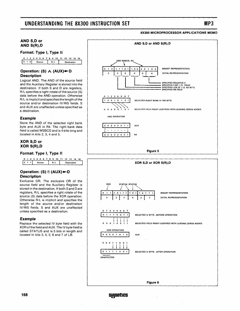
UNDERSTANDING THE 8X300 INSTRUCTION SET MP3
AND S,D or AND S(R),D
Format: Type I, Type II o 1 2 3 4 5 6 7 8 9 10 11 12 13 14 15
I 0 1 0 I Source I RIL I Destination
Operation: (S) A (AUX)~D Description Logical AND. The AND of the source field and the Auxiliary Register is stored into the destination. If both Sand D are registers, R/L specifies a right rotate of the source (S) data before the AND operation. Otherwise R/L is implicit and specifies the length of the source andlor destination IV/WS fields. S and AUX are unaffected unless specified as a destination.
Example Store the AND of the selected right bank byte and AUX in R4. The right bank data field is called WSBCD and is 4 bits long and located in bits 2, 3, 4 and 5.
XOR S,D or XOR S(R),D
Format: Type I, Type II o 1 2 3 4 5 6 7 8 9 10 11 12 13 14 15
10 1 1 I Source I RIL I Destination
Operation: (S) (!) (AUX)~D Description Exclusive OR. The exclusive OR of the source field and the Auxiliary Register is stored in the destination. If both Sand Dare registers, R/L specifies a right rotate of the source (S) data before the XOR operation. Otherwise R/L is implicit and specifies the length of the source andlor destination IV IWS fields. Sand AUX are unaffected unless specified as a destination.
Example Replace the selected IV byte field with the XOR of the field and AUX. The IV byte field is called STATUS and is 5 bits in length and located in bits 3, 4, 5, 6 and 7 of LB.
168
8X300 MICROPROCESSOR APPLICATIONS MEMO
AND S,D or AND S(R),D
T BINARY REPRESENTATION
OCTAL REPRESENTATION
'---- SPECIFIES REGISTER 4 SPECIFIES 4·BIT 110 FIELD
L_~========== SPECIFIES LSB OF 110 AS BIT 5 SPECIFIES RB FIELD
01234567
/1 0 0 1 0 1 0 1 I ~~
00000101
AND OPERATION
I 0 0 o 0 0 0 1 1 I ! !
I 0 0 o 0 0 o 0 1 I
o 1 2 3 4 5 6 7
I 0 1 1 1 0 0 1 1 I ! ! ! ! !
00010011
XOR OPERATION
00011001
! J ! ! J I 0 1 1 1 1 0 0 1 I ---UNAFFECTED
Smnotics
SELECTED RIGHT BANK IVIWS BYTE
SELECTED FIELD RIGHT JUSTIFIED WITH LEADING ZEROS ADDED.
AUX
R4
Figure 5
XOR S,D or XOR S(R),D
BINARY REPRESENTATION
OCTAL REPRESENTATION
SELECTED IV BYTE-BEFORE OPERATION
SELECTED FIELD RIGHT-JUSTIFIED WITH LEADING ZEROS ADDED
AUX
SELECTED IV BYTE-AFTER OPERATION
Figure 6
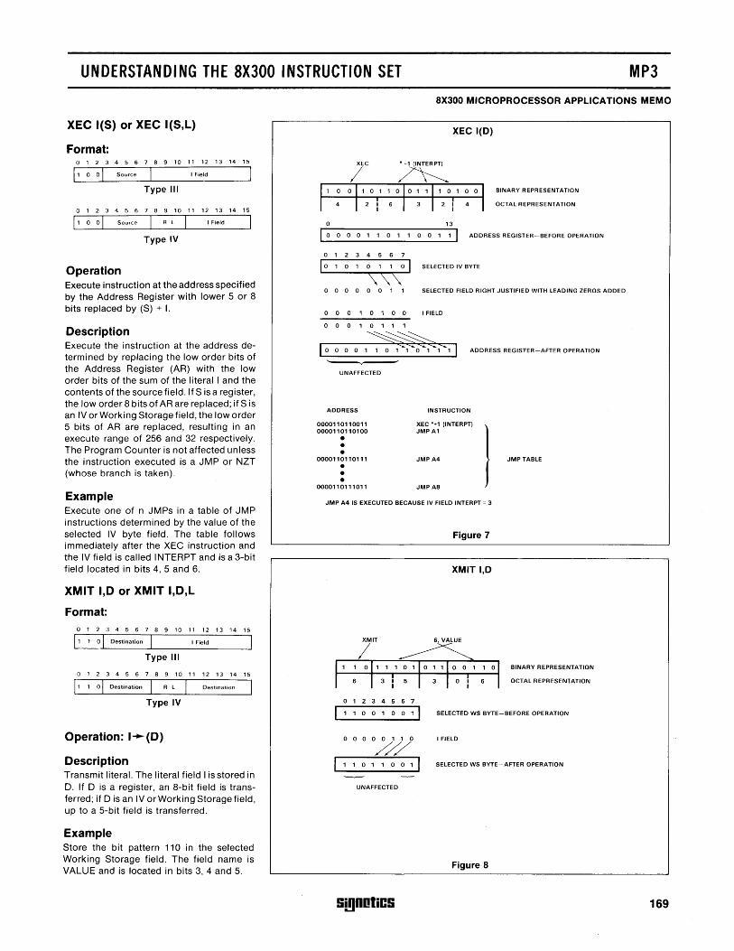
UNDERSTANDING THE 8X300 INSTRUCTION SET MP3
XEC I{S) or XEC I{S,L)
Format: o 1 2 3 4 5 6 7 8 9 10 11 12 13 14 15
11 0 0 1 Source I Field
Type III
o 1 2 3 4 5 6 7 8 9 10 11 12 13 14 15
11 0 0 1 Source R L I Field
Type IV
Operation Execute instruction at the address specified by the Address Register with lower 5 or 8 bits replaced by (S) + I.
Description Execute the instruction at the address determined by replacing the low order bits of the Address Register (AR) with the low order bits of the sum of the literal I and the contents of the source field. If S is a register, the low order 8 bits of AR are replaced; if Sis an IV or Working Storage field, the low order 5 bits of AR are replaced, resulting in an execute range of 256 and 32 respectively. The Program Counter is not affected unless the instruction executed is a JMP or NZT (whose branch is taken).
Example Execute one of n JMPs in a table of JMP instructions determined by the value of the selected IV byte field. The table follows immediately after the XEC instruction and the IV field is called INTERPT and is a 3-bit field located in bits 4, 5 and 6.
XMIT I,D or XMIT I,D,L
Format: 0 1 2 3 4 5 6 7 8 9 10 11 12 13 14
11 1 01 Destination 1
I Field
Type III
0 1 2 3 4 5 6 7 8 9 10 11 12 13 14
11 1 0 I Destination I R L Destination
Type IV
Operation: I~ (D)
Description
15
15
Transmit literal. The literal field I is stored in D. If 0 is a register, an 8-bit field is transferred; if 0 is an IV orWorking Storage field, up to a 5-bit field is transferred.
Example Store the bit pattern 110 in the selected Working Storage field. The field name is VALUE and is located in bits 3, 4 and 5.
8X300 MICROPROCESSOR APPLICATIONS MEMO
XEC 1(0)
BINARY REPRESENTATION
OCTAL REPRESENTATION
13
I 0 0 0 0 1 1 0 1 1 0 0 1 1 I ADDRESS REGISTER-BEFORE OPERATION
01234567
10 1 o 1 0 1 1 0 I SELECTED IV BYTE
\\\ 00000011 SELECTED FIELD RIGHT JUSTIFIED WITH LEADING ZEROS ADDED
00010100 I FIELD
o 0 0 1 0 1 1 1
I ~<;: 0000110110111 ADDRESS REGISTER-AFTER OPERATION
-.,-UNAFFECTED
ADDRESS INSTRUCTION
0000110110011 XEC *+1 (INTERPT)
I 0000110110100 JMPAl
• • • 0000110110111 JMPA4 JMP TABLE
• • • 0000110111011 JMPA8
JMP A4 IS EXECUTED BECAUSE IV FIELD INTERPT = 3
Figure 7
XMIT I,D
BINARY REPRESENTATION
OCTAL REPRESENTATION
o 1 234 5 6 7
1 1 0 0 1 0 0 1 I SELECTED WS BYTE-BEFORE OPERATION
00000110 I FIELD
/// 1 1 0 1 1 0 0 1 I SELECTED WS BYTE-AFTER OPERATION
UNAFFECTED
Figure 8
!ii!ln~tiC!i 169
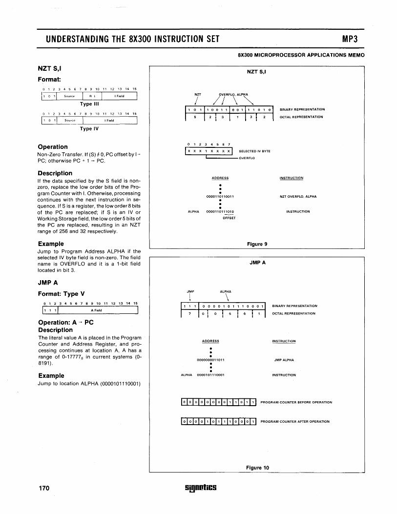
UNDERSTANDING THE 8X300 INSTRUCTION SET MP3
NZTS,I
Format: o 1 2 3 4 5 6 7 8 9 10 11 12 13 14 15
11 0 1 1 Source R L I Field
Type III
o 1 2 3 4 5 6 7 8 9 10 11 12 13 14 15
11 0 1 1 Source I Field
Type IV
Operation Non-Zero Transfer. If (S) f 0, PC offset by 1-PC; otherwise PC + 1 -+ PC.
Description If the data specified by the S field is nonzero, replace the low order bits of the Program Counter with I. Otherwise, processing continues with the next instruction in sequence. If S is a register, the low order 8 bits of the PC are replaced; if S is an IV or Worki ng Storage field, the low order 5 bits of the PC are replaced, resulting in an NZT range of 256 and 32 respectively.
Example Jump to Program Address ALPHA if the selected IV byte field is non-zero. The field name is OVERFLO and it is a 1-bit field located in bit 3.
JMPA
Format: Type V o 1 2 3 4 5 6 7 8 9 10 11 12 13 14 15
11 1 11 A Field
Operation: A -+ PC Description The literal value A is placed in the Program Counter and Address Register, and processing continues at location A. A has a range of 0-177778 in current systems (0-8191).
Example Jump to location ALPHA (0000101110001)
170
8X300 MICROPROCESSOR APPLICATIONS MEMO
NZT 5,1
01234567
I x x X 1 X X X x I SELECTED IV BYTE
OIiERFLO
ADDRESS
• • • 0000110110011
• • • ALPHA 0000110111010
OFFSET
ALPHA
\
Figure 9
JMPA
0000101110001
ALPHA
o I I
ADDRESS
• • • 0000000011011
• • • 0000101110001
I 6 I 1 I I
BINARY REPRESENTATION
OCTAL REPRESENTATION
INSTRUCTION
NZT OVERFLO, ALPHA
INSTRUCTION
BINARY REPRESENTATION
OCTAL REPRESENTATION
INSTRUCTION
JMP ALPHA
INSTRUCTION
1 0 1 0 1 0 1 0 1 0 1 01 0 1 0 11 11 1 0 11 11 1 PROGRAM COUNTER BEFORE OPERATION
1 01 0 10 1 0 11 1011 11 11 101 01011 1 PROGRAM COUNTER AFTER OPERATION
Figure 10
!ii!)DotiC!i
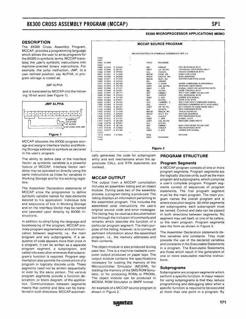
8X300 CROSS ASSEMBLY PROGRAM (MCCAP) SPI
DESCRIPTION The 8X300 Cross Assembly Program, MCCAP, provides a programming language which allows the user to write programs for the 8X300 in symbolic terms. MCCAPtranslates the user's symbolic instructions into machine-oriented binary instructions. For example, the jump instruction, ~MP, to a user defined position, say ALPHA, in program storage is coded as:
JMP ALPHA
and is translated by MCCAP into the following 16-bit word (see Figure 1).
JMPALPHA
o 15
111111101011111010101111101010111
~ I ~i (EXAMPLE) I
n LOCATION OF ALPHA > OP CODE FOR JMP
Figure 1
MCCAP allocates the 8X300 program storage and assigns Interface Vector and Working Storage address to symbols as declared in the user's program.
The ability to define data of the Interface Vector as symbolic variables is a powerful feature of MCCAP. Interface Vector variables may be operated on directly using the same instructions as those for variables in Working Storage and for the working registers.
The Assembler Declaration statements of MCCAP allow the programmer to define symbolic variable names for data elements tai lored to his appl ication. I nd ividual bits and sequences of bits in Working Storage and on the I nterface Vector may be named and operated upon directly by 8X300 instructions.
In addition to simplifying the language and bookkeeping of the program, MCCAP provides program segmentation and communication between segments; i.e., the main program and any subprograms. If a sequence of code appears more than once in a program, it can be written as a separate program segment, a subprogram, and called into execution whenever that subprogram's function is required. Program segmentation also permits the construction of a program in logically discrete units. These segments need not be written sequentially or even by the same person. The various program segments provide a function description, or block diagram, of the application. Communication between segments means that control and data can be transferred in both directions. MCCAP automati-
8X300 MICROPROCESSOR APPLICATIONS MEMO
MCCAPSOURCEPROGRAM
MICROCONTROLLER SYMBOLIC ASSEMBLER VER 1.0
1680 1681 1682 01544 PROC RDCMMD 1683 1684 01544 6 07003 SEL IVRESP FOC RESPONSE 8YTE 1685 01545 6 20101 XMIT UR. BCTRL ESTA8LiSH USER READ ONLY 1686 01546 6 07002 SEL IVDATA HOLDS COMMAND BYTE 1687 01547 o 27305 MOVE FUNC. R5 FUNCTION CODE 1688 01550 o 24306 MOVE DADDR. R6 DISK ADDRESS 1689 01551 o 21202 MOVE BUFF. R2 BUFFER FUNCTION CODE 1690 01552 6 07003 SEL IVRESP 1691 01553 6 25100 XMIT O. DONE SHOW COMMAND IN PROGRESS 1692 01554 6 20100 XMIT UW, BCTRL RESTORE USER WRITE 1693 01555 6 27101 XMIT 1, XFR SIGNAL USER FDC ACCEPTED BYTE 1694 01556 6 07001 SEL IVCTRL USER CONTROL BYTE 1695 01557 5 26117 NZT CMMD," WAIT FOR CMMD TO GO LOW 1696 01560 6 07003 SEL IVRESP FDC RESPONSE BYTE 1697 01561 6 27100 XMIT 0, XFR LOWER XFR SIGNAL 1698 01562 607001 SEL IVCTRL USER CTRL BYTE 1699 01563 426123 XEC "(CMMD), 2 WAIT FOR NEXT COMMAND SIGNAL 1700 01564 6 07003 SEL IVRESP SECOND COMMAND BYTE AVAILABLE 1701 01565 6 20101 XMIT UR, BCTRL SET IVDATA TO USER READ ONLY 1702 01566 6 07002 SEL IVDATA 2ND COMMAND BYTE 1703 01567 o 27704 MOVE TRACK, R4 TRACK ADDRESS 1704 01570 o 27503 MOVE SECT, R3 SECTOR ADDRESS 1705 01571 6 07003 SEL IVRESP FDC RESPONSE BYTE 1706 01572 6 27101 XMIT 1, XFR SIGNAL USER 1707 01573 6 20100 XMIT UW, BCTRL RESTORE USER WRITE 1708 01574 607001 SEL IVCTRL 1709 01575 5 26135 NZT CMMD," WAIT FOR CMMD TO GO LOW 1710 01576 6 07003 SEL IVRESP FDC RESPONSE BYTE 1711 01577 6 27100 XMIT 0, XFR LOWER XFR SIGNAL 1712 1713 01600 7 01652 RTN RETURN 1714 END RDCMMD 1715
Figure 2
cally generates the code for subprogram entry and exit mechanisms when the appropriate CALL and RTN statements are invoked.
MCCAP OUTPUT The output from a MCCAP compilation includes an assembler listing and an object module. During pass two of the assembly process, a program listing is produced. The listing displays all information pertaining to the assembled program. This includes the assembled octal instructions, the user's original source code and error messages. The listing may be used as a documentation tool through the inclusion of comments and remarks which describe the function of a particular program segment. The main purpose of the listing, however, is to convey all pertinent information about the assembled program, i.e., the memory addresses and their contents.
The object module is also produced during pass tWQ. This is a machine-readable computer output produced on paper tape. The output module contains the specifications necessary for loading the memory of the Microcontroller Simulator (MCSIM), for loading the memory of the SMS ROM Simulator, or for producing ROMs or PROMs. The object module can be produced in MCSIM, ROM Simulator or BNPF format.
An example of a MCCAP source program is shown in Figure 2.
S!!I0otiCS
PROGRAM STRUCTURE
Program Segments A MCCAP program consists of one or more program segments. Program segments are the logically discrete units, such as the main program and subprograms, which comprise a user's complete program. Program segments consist of sequences of program statements. The first program segment must be the main program. The main program names the overall program and is where execution begins. All other segments are subprograms; each subprogram must be named. Control and data can be passed in both directions between segments. No segment may call itself, or one of its callers, or the main program. Program segments take the form as shown in Figure 3.
The Assembler Declaration statements define variables and constants. They must precede the use of the declared variables and constants in the Executable Statements in a program. The Executable Statements are those which result in the generation of one or more executable machine instructions.
Subprograms Subprograms are program segments which perform a specific function. A major reason for using subprograms is that they reduce programming and debugging labor when a specific function is required to be executed at more than one point in a program. By
171
8X300 CROSS ASSEMBLY PROGRAM (MCCAP) SPI
8X300 MICROPROCESSOR APPLICATIONS MEMO
PROGRAM SEGMENTS
PROGRAM STATEMENT DECLARATION STATEMENT(S)
• • • EXECUTABLE STATEMENT(S)
• • SUBPROGRAMS
• END STATEMENT
a. Main Program Form
PROCEDURE STATEMENT DECLARATION STATEMENT(S)
• • • EXECUTABLE STATEMENT(S)
• • • END STATEMENT
b. Subprogram Form
Figure 3
creating the required function as a subprogram, the statements associated with that function may be coded once and executed at many different points in a program. Figure 3 illustrates an example.
The program structure in Figure 3 causes the code associated with PROC WAIT to be executed three times within PROG MANYWAIT. This is accomplished even though the statements associated with PROC WAIT are coded only once, rather than three times.
Subprogram Calls and Returns For user-provided procedures, a jump to the associated procedure and a return link are created for each procedure reference. The instructions to accomplish this result in subprogram entry time. The instructions to accomplish subprogram exit result in exit time. The user may utilize the MCCAP procedure mechanism for linking calling programs with called programs or he may create his own instructions to do so. The following describes the linkage mechanism and timing for MCCAP user procedures.
Linkage between called and calling programs is achieved through the generation of an indexed "return jump" table, the length of which corresponds to the number of different times in the program that the subprograms are called. This table is generated automatically by MCCAP when procedure CALL and RTN statements are invoked. For each procedure reference, MCCAP creates two statements in the calling program. Thus, the time required for the subprogram entry is 0.5 microseconds. The subprogram
172
return mechanism requires the execution of two instructions or 0.5 microseconds. These times do not include saving and restoring of the working registers. The total time to save all working registers is 3.5 microseconds, the same time to restore all registers. Saving of all working registers is normally not necessary, but worst case calculations for entry and exit time below do include this time. Thus, subprogram exit and entry times are:
O.5f.1s :::; Entry Time:::; 4.0f.1s O.5f.1s :::; Exit Time:::; 4.0f.1s
Details of the code required for procedure CALL and RTN are provided in the Programming Examples section. See Figures 21 and 22.
Macros A macro is a sequence of instructions that can be inserted in the assembly source text by encoding a Single instruction. The macro is defined only once and may then be invoked any number of times in the program. This facility simplifies the coding of programs, reduces the chance of errors, and makes programs easier to change.
A macro definition consists of a heading, a body and a terminator. This definition must precede any calion the macro. In MCCAP, the heading consists of the MACRO statement which marks the beginning of the macro and names it. The body of the macro is made up of those MCCAP statements which will be inserted into the source code in place of the macro call. The terminator consists of an ENDM statement which marks the physical end of the macro definition.
MCCAP Statements The MCGAP language consists of thirty statements categorized as follows:
Assembler Directive Statements Assembler Declaration Statements Communication Statements Macro Statements Machine Statements
The following lists the statements in each category, describes their use, and provides examples. Detailed use of the instructions including rules of syntax and parameter restrictions are described in the MGGAp Reference Manual.
Assembler Directive Statements Assembler Directive statements define program structure and control the assembler outputs. They do not result in the generation of 8X300 executable code. There are twelve Assembler Directive statements:
PROG Statement PROC Statement
Si!lDOliCS
ENTRY Statement END Statement ORG Statement OBJ Statement IF Statement ENDIF Statement LIST Statement NLIST Statement EJCT Statement SPAC Statement
PROG Statement Use Defines the names and marks the beginning of a main program.
Example: PROG PROCESS
PROC Statement Use Defines the names and marks the beginning of a subprogram.
Example: PROC WAIT
ENTRY Statement Use Defines the name and marks the location of a secondary entry point to a subprogram.
Example: ENTRY POINT 2
END Statement Use Terminates a program segment or a complete program.
Examples: END SUB1 END MAIN
ORG Statement Use Sets the prog ram counter to the val ue specified in the operand field.
Example: ORG 200
OBJ Statement Use To specify the format of the object module.
Examples: OBJ R
NOTE
OBJ M OBJ N
"R" indicates the ROM Simulator format. "M" indicates the Microcontroller Simulator format. "N" indicates BNPF for
mat·
IF Statement Use To mark the beginning of a sequence of code, which mayor may not be assembled depending on the value of an expression.
Examples: IF VAL IF X + Y
8X300 CROSS ASSEMBLY PROGRAM (MCCAP) SPI
ENDIF Statement Use To mark the end of sequence of code, which is to be conditionally assembled. In the case of nested IF statements, an ENDIF is paired with the most recent IF.
Example: ENDIF
II ST Statement Use To select and control output of a MCCAP assembly.
Example: LIST S,O,M,I
NliST Statement Use To suppress elements of the output from a MCCAP assembly.
Example: NLiST O,M,I
EJCT Statement Use To cause the output listing to be advanced to the next page.
Example: EJCT
SPAC Statement Use To insert blank lines into the output listing. The number of lines inserted is indicated in the operand field.
Example: SPAC 3
Assembler Declaration Statement Assembler Declaration statements define and describe the data, constants and variables, in a program or subprogram. There are four Assembler Declaration statements:
EQU Statement SET Statement LlV Statement RIV Statement
EQU Statement Use To define a fixed constant.
Examples: FIVE EQU 5 ON EQU 1
SET Statement Use To define and assign a value to a constant, which may later be assigned a new value by another SET statement.
Example: OFF SET 0
8X300 MICROPROCESSOR APPLICATIONS MEMO
lIV Statement Use To define and assign symbolic names to variables, usually IV bytes, located on the left bank of the Interface Vector.
Example: LITE LlV 23,2,1
NOTE
The effect of the above example is to define a variable whose name is LITE. It is located in a byte whose addresS is 23. The right-most bit of LITE is bit 2 and its length is 1 bit.
R IV Statement Use To define and assign symbolic names to variables, usually in Working Storage, located on the right bank of the Interface Vector.
Example: DATA RIV 200,6,3
NOTE
The effect of the above example is to define a variable whose name is DATA. It is located in a byte whose address is 200. The right-most bit DATA is bit 6 of the byte and its length is 3 bits.
Communication Statements Communication statements are executable statements which provide the mechanism for main program to subprogram linkage. They provide the means by which subprograms are called and returned from. There are two kinds of Communication statements:
CALL Statement RTN Statement
CALL Statement Use To transfer control from a calling program to the called subprogram. The CALL statement causes the generation of two 8X300 instructions.
Examples: CALL WAIT CALL SINE
NOTE
The above are valid statements to be coded into the program if WAIT and SINE have been defined in PROC statements. The effect of invoking these statements is to transfer execution control to the procedures WAIT and SINE respectively.
RTN Statement Use To transfer control from a called subprogram to a calling program.
Example: RTN
S!!IDotiCS
Macro Statements Macro statements provide the mechanism for defining macros and for inserting them into the source code. There are three Macro statements:
MACRO Statement ENDM Statement MACRO CALL Statement
MACRO Statement Use To mark the beginning of a macro definition. The MACRO statement forms the heading of the macro definition.
E~mp~~ MAC1 MACRO MAC2 MACRO A,B,C
NOTE
The second example would mark the beginning of a macro called MAC2. The "A,B,C" represents a formal parameter list. These parameters, used in writing the macro body, will be replaced by the actual parameters listed in the MACRO CALL statement.
ENDM Statement Use To mark the end of a macro definition. The ENDM statement forms the terminator of the macro definition.
Example: ENDM
MACRO CALL Statement Use To indicate where a macro is to be inserted into the source code and to specify any actual parameters needed by the macro.
Example: MAC2 DATA, INPUT, RESULT
NOTE
There is no single macro call statement. Any macro name which has been defined as such may be coded as if it were a valid MCCAP statement. The macro name is coded in the operation field and the actual parameters are placed in the operand field.
Machine Statement Machine statements are the MCCAP symbolic representations of the 8X300 executable statements. Machine statements have a one to one correspondence to 8X300 instructions. Each Machine statement results in the generation of a single 8X300 ihstruction. There are eight Machine statements:
MOVE Statement ADD Statement AND Statement XOR Statement XMIT Statement XEC Statement NZT Statement JMP Statement
173
8X300 CROSS ASSEMBLY PROGRAM (MCCAP) SPI
8X300 MICROPROCESSOR APPLICATIONS MEMO
MOVE statement Use To copy the contents of a specified register, WS variable or IV variable into a specified register, WS or IV. Defihed in Instruction Descri ptions.
Examples: MOVE R1 (6);R6 MOVE X,Y
NOTE
The first example illustrates a six place right rotate of Rl 's data before it is moved to R6. The contents of Rl are neit affected. The second example may be a Working Storage or Interface Vector variable move. depending on the way X and Yare defined in Declaration Statements.
ADO Statement Use To add the contents of a specified register, WS variable, or IV variable to the contents of the AUX register and place the result in a specified register, WS variable or IV variable.
Examples: ADD R1 (3),R2 ADD DATA,OUTPUT
NOTE
The first example illustrates a three place right rotate of Rl's data before the addition is carried out. Under certain conditions a rotate may be used to multiply the specified operand by a power of 2 before the additiOn is done. The contents of I'll are nco affected. The second example suggests that the contents of WS variable have been added to the contents of the AUX register and the result placed in an IV variable, making the result immediately available to the user's system.
AN 0 Statement Use To compute the logical AND of the contents of a specified register, WS variable or IV variable and the contents of the AUX register. The logical result is placed in a specified register, WS variable or IV variable. In actual practice, the AND statement is often used to mask out undesired bits of a register.
Examples: AND R2,R2
NOTE
AND R3(1),R5 AND X,V
The first example illustrates the use of an AND statement in what might be a masking operation. If the AUX register contains 00001111 then this statement sets the 4 high order bits of R2 to 0 no matter what they were originally. The 4 loW order bits of R2 would be unaffected.
The second example illustrates a one place rotate to the right of R3's data before the AND is carried out. The contents of R3 are not affected. In the third example, X and Y may be parts of the same WS or IV byte, or one may be a WS byte and the other an IV byte.
XOR Statement Use To compute the logical exclusive OR of the contents of a specified register, WS variable
174
or IV variable and the contents of the AUX register, and place the result in a specified register, WS variable or IV variable. In practice, the XOR statement is often used to complement a value and to perform comparisons.
Examples: XOR R6,R11 XOR R1 (7),R4 XOR X,Y
NOTE
The first example illustrates the use of an XOR statement in what might be a complementing operation. If the AUX register contains all 1 's then the execution of this statement results in the complement of the contents of R6 replacing the contents of Rll. The second and third examples are of the same form as the second and third examples of the AND statement.
XMIT Statement Use To transmit or load literal values into registers, WS variables or IV variables.
Examples: XMIT DATA,IVR
NOTE
XMIT OUTPUT,IVL XMIT -11 ,AUX XMIT -00001011 B,AUX XMIT -13H,AUX
The first example selects a previously declared WS variable by transmitting its address to the IVR register. The second example selects a previously declared IV variable by transmitting its address to the IVL register. The last three examples all result in the generation of the same machine code. They all load the AUX register with -11 ,0 , In the first case, the programmer has written the number in base 10. In the second case, the programmer has written the number in binary and has indicated this by placing a B after the number. In the third case, the number has been written in octal as indicated by an H after the number.
XEC Statement Use To select and execute one instruction out of a list of instructions in program memory as determined by the value of a data variable, and then continue the sequential execution of the program beginning with the statement immediately fol/owing the XEC unless the selected instruction is a JMP or NZT statement.
Examples: XEC JTABLE(R1),3
JTABLE JMP GR8ERTHAN
SEND
JMP LESSTHAN JMP EQUALTO
XEC SEND(INPUT),4 "NEXT INSTRUCTION" "NEXT INSTRUCTION"
XMIT 11011011B,AUX XMIT 11111111B,AUX XMIT 10101010B,AUX XMIT OOOOOOOOB,AUX
Si!Jnntics
NOTE
In the first example, the execution of the program will transferred to one of three labeled instructions on the basis of whether register Rl contains 0, 1 or 2. In the second example, the XEC statement causes the execution of a statement which transmits a special bit pattern to the AUX register in response to an input signal which is eitherO, 1,2 or 3. After the pattern is transmitted, the execution of the program continues with the next instruction after the XEC.
NZT Statement Use To carry out a conditional branch on the basis of whether or not a register, WS variable, or IV variable is zero or non-zero.
Examples: NZT R1 ,*+2 NZT SIGN,NEG
NOTE
In the first example, if the contents of Rl are non-zero, then program execution will continue with the instruction, whose address is the sum of the address of the NZT statement and 2. If the contents of Rl are 0, the program execution continues with the next instruction after the NZT statement. In the second example, if the contents of a WS or IV variable called SIGN is non-zero, then program execution will continue beginning with the instruction whose address is NEG. Otherwise execution continues with the next instruction after the NZT statement.
JMP Statement Use To transfer execution of the program to the statement whose address is the operand of the JMP statement.
Examples: JMP START JMP *-2
NOTE
In the first example, execution of the program continues sequentially beginning with the instruction labeled START. In the second example, program execution continues beginning with the instruction whose address is the JMP instruction's address minus 2.
SEL Statement Use Select a variable in Working Storage or on the Interface Vector, so that subsequent machine instructions may reference that variable.
Examples: SEL DATA SEL OUTPUT
NOTE
It is the programmer's responsibility to assure that the proper page has been addressed before calling the SEL statement if the variable may be in Working Storage. The SEL statement causes a single instruction, XMIT, to be assembled into the user program. The operand of the XMIT instruction is the byte address of the named variable (argument of the reference) as it has been allocated in Working Storage or on the Interface Vector.·
PROGRAMMING EXAMPLES This section contains programming examples which demonstrate how the 8X300's instructions can be assembled to perform some simple, commonly required functions. These examples are written as program
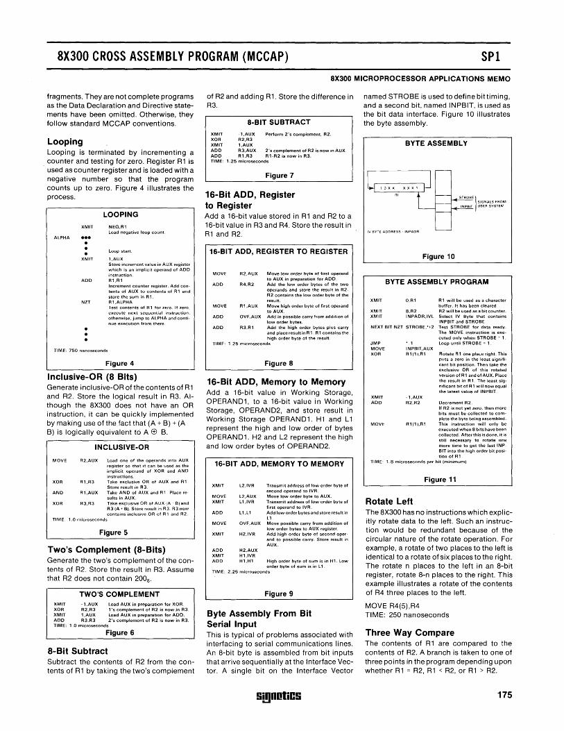
8X300 CROSS ASSEMBLY PROGRAM (MCCAP) SPI
fragments. They are not complete programs as the Data Declaration and Directive statements have been omitted. Otherwise, they follow standard MCCAP conventions.
Looping Looping is terminated by incrementing a counter and testing for zero. Register R1 is
, used as counter register and is loaded with a negative number so that the program counts up to zero. Figure 4 illustrates the process.
ALPHA
XMIT
••• • • • XMIT
ADD
NZT
• • •
LOOPING
NEG,R1 Load negative loop count.
loop start.
1,AUX Store increment value in AUX register which is an implicit operand of ADD instruction. R1,R1 Increment counter register. Add contents of AUX to contents of R 1 and store the sum in R 1. R1,AlPHA Test contents of R1 for zero. If zero, execute next sequential instruction, otherwise, jump to ALPHA and continue execution from there.
TIME: 750 nanoseconds
Figure 4
Inclusive-OR (a Bits) Generate inclusive-OR of the contents of R1 and R2. Store the logical result in R3. Although the 8X300 does not have an OR instruction, it can be quickly implemented by making use of the fact that (A + B) + (A B) is logically equivalent to A Ef) B.
INCLUSIVE-OR
MOVE R2,AUX load one of the operands into AUX register so that it can be used as the implicit operand of XOR and AND instructions.
XOR R 1 ,R3 Take exclusive OR of AUX and R 1 Store resu It in R 3.
AND R 1 ,AUX Take AND of AUX and R 1. Place results in AUX.
XOR R3,R3 Take exclusive OR of AUX IA . 8) and R3 (A + B). Store result'" R3. R3 now contains inclusIve OR of R 1 and R2.
TIME 1.0 microseconds
Figure 5
Two's Complement (a-Bits) Generate the two's complement of the contents of R2_ Store the result in R3. Assume that R2 does not contain 2008,
TWO'S COMPLEMENT XMIT -1,AUX load AUX in preparation for XOR. XOR R2,R3 1 's complement of R2 is now in R3. XMIT 1,AUX load AUX in preparation for ADD. ADD R3,R3 2's complement of R2 is now in R3. TIME: 1.0 microseconds
Figure 6
a-Bit Subtract Subtract the contents of R2 from the contents of R1 by taking the two's complement
aX300 MICROPROCESSOR APPLICATIONS MEMO
of R2 and adding R1. Store the difference in R3.
a-BIT SUBTRACT
XMIT -1,AUX Perform 2's complement, R2. XOR R2,R3 XMIT 1,AUX ADD R3,AUX 2's complement of R2 is now in AUX. ADD R1,R3 R1·R2 is now in R3. TIME: 1.25 microseconds
Figure 7
16-Bit ADD, Register to Register Add a 16-bit value stored in R1 and R2 to a 16-bit value in R3 and R4. Store the result in R1 and R2.
16-BIT ADD, REGISTER TO REGISTER
MOVE R2,AUX Move low order byte of first operand to AUX in preparation for ADD.
ADD R4,R2 Add the low order bytes of the two operands and store the result in R2. R2 contains the low order byte of the result.
MOVE R1,AUX Move high order byte of first operand to AUX.
ADD OVF,AUX Add in possible carry from addition of low order bytes.
ADD R3,R 1 Add the high order bytes plus carry and place result in R 1. R 1 contains the high order byte of the result.
TIME: 1.25 microseconds
Figure a
16-Bit ADD, Memory to Memory Add a 16-bit value in Working Storage, OPERAND1, to a 16-bit value in Working Storage, OPERAND2, and store result in Working Storage OPERAND1, H1 and L 1 represent the high and low order of bytes OPERAND1. H2 and L2 represent the high and low order bytes of OPERAND2,
16,;.BIT ADD, MEMORY TO MEMORY
XMIT l2,IVR Transmit address of low order byte of second operand to IVR.
MOVE l2,AUX Move low order byte to AUX. XMIT l1,IVR Transmit address of low order byte of
first operand to IVR. ADD l1,l1 Add low order bytes and store result in
l1. MOVE OVF,AUX Move possible carry from addition of
low order bytes to AUX register. XMIT H2,IVR Add high order byte of second oper
and to possible carry. Store result in AUX.
ADD XMIT ADD
H2,AUX H1,IVR H1,H1 High order byte of sum is in H1. low
order byte of sum is in l1. TIME: 2.25 microseconds
Figure 9
Byte Assembly From Bit Serial Input This is typical of problems associated with interfacing to serial communications lines, An 8-bit byte is assembled from bit inputs that arrive sequentially at the Interface Vector. A single bit on the Interface Vector
G!!I0otiCG
named STROBE is used to define bit timing, and a second bit, named INPBIT, is used as the bit data interface, Figure 10 illustrates the byte assembly,
BYTE ASSEMBLY
IV BYTE ADDRESS, INPADR
XMIT
Figure 10
BYTE ASSEMBLY PROGRAM
0,R1 R1 will be used as a character buffer. It has been cleared.
XMIT 8,R2 R2 will be used as a bit counter. XMIT INPADR,IVl Select IV Byte that contains
INPBIT and STROBE. NEXT BIT NZT STROBE:+2 Test STROBE for data ready.
JMP MOVE XOR
XMIT ADD
MOVE
*-1 INPBIT,AUX R1(1),R1
-1,AUX R2,R2
R1(1),R1
The MOVE instruction is executed only when STROBE c 1. loop until STROBE c 1.
Rotate R 1 one pla<.e right. This puts a zero in the least signifi~ cant bit pOSition. Then take the exclusive OR of this rotated version of R1 and of AUX. Place the result in R 1. The least significant bit of R 1 will now equal the latest value of INPBIT.
Decrement R2. If R 2 is not yet zero, then more bits must be collected to complete the byte being assembled. This instruction will only be executed when 8 bits have been COllected. Afterthis is done, it is still necessary to rotate one more time to get the last INPBIT into the high order bit position of R1.
TIME: 1.8 microseconds per bit (minimum)
Figure 11
Rotate Left The 8X300 has no instructions which explicitly rotate data to the left. Such an instruction would be redundant because of the circular nature of the rotate operation, For example, a rotate of two places to the left is identical to a rotate of six places to the right. The rotate n places to the left in an 8-bit register, rotate 8-n places to the right. This example illustrates a rotate of the contents of R4 three places to the left.
MOVE R4(5),R4 TIME: 250 nanoseconds
Three Way Compare The contents of R1 are compared to the contents of R2, A branch is taken to one of three points in the program depending upon whether R1 = R2, R1 < R2, or R1 > R2,
175
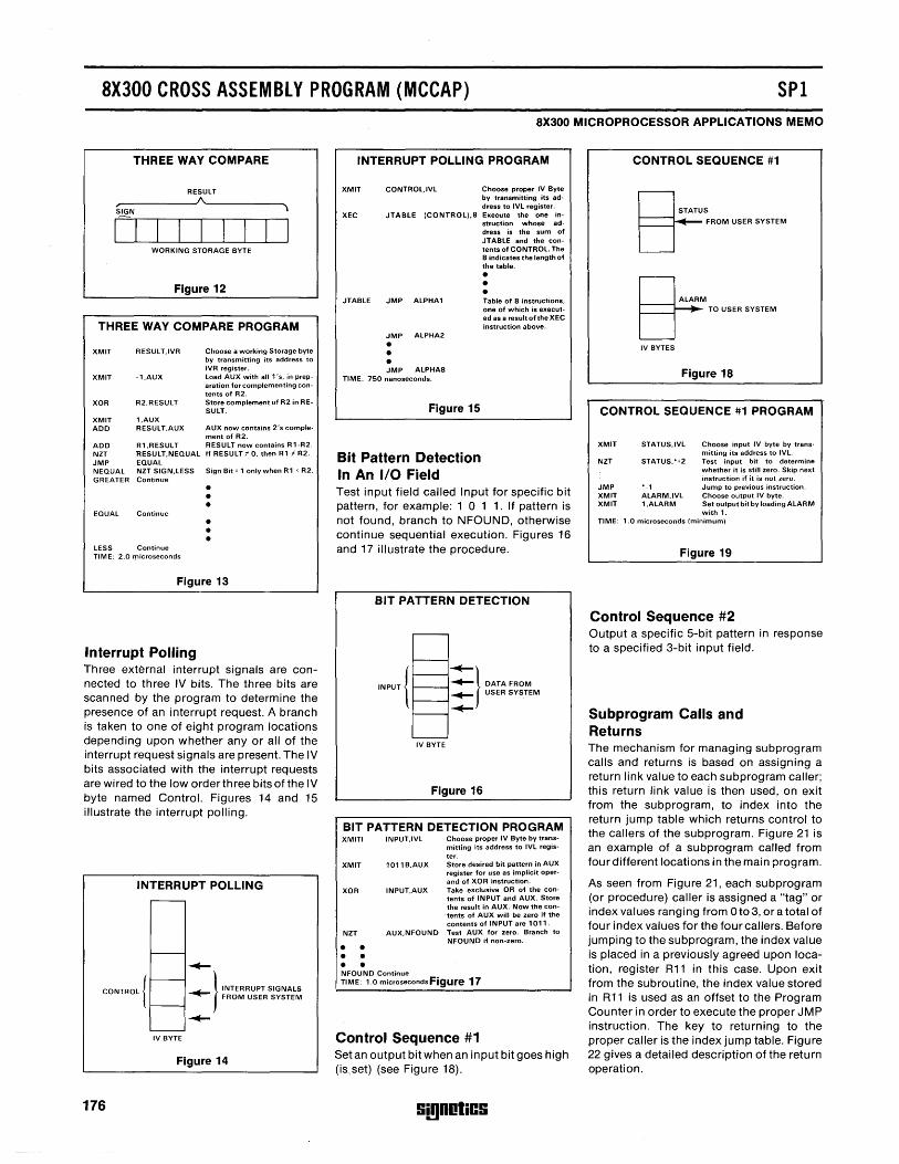
8X300 CROSS ASSEMBLY PROGRAM (MCCAP) SPI
THREE WAY COMPARE
RESULT ,-__________ ~A~ __________ ~ SIGN ,
I I I I I I I I I WORKING STORAGE BYTE
Figure 12
THREE WAY COMPARE PROGRAM
XMIT RESULT,IVR Choose a working Storage byte by transmitting its address to IVR register,
XMIT -1,AUX Load AUX with all 1's, in prep-aration for complementing con-tents of R2.
XOR R2,RESULT Store complement of R2 in RE-SULT,
XMIT 1,AUX ADD RESULT,AUX AUX now contains 2's comple-
ment of R2. ADD R1,RESULT RESULT now contains R 1-R2. NZT RESULT,NEQUAL If RESULT I' 0, then R1 I'R2. JMP EQUAL NEQUAL NZT SIGN,LESS Sign Bit = 1 only when R1 < R2. GREATER Continue
• • • EQUAL Continue
• • • LESS Continue TIME: 2.0l)1icroseconds
Figure 13
Interrupt Polling Three external interrupt signals are connected to three IV bits_ The three bits are scanned by the program to determine the presence of an interrupt request. A branch is taken to one of eight program locations depending upon whether any or all of the interrupt request signals are present. The IV bits associated with the interrupt requests are wired to the low order three bits of the IV byte named Control. Figures 14 and 15 illustrate the interrupt polling_
INTERRUPT POLLING
CONTROL (
176
IV BYTE
~
~} INTERRUPT SIGNALS FROM USER SYSTEM
~
Figure 14
8X300 MICROPROCESSOR APPLICATIONS MEMO
INTERRUPT POLLING PROGRAM
XMIT
XEC
JTABLE
CONTROL,IVL Choose proper IV Byte by transmitting its address to IVL register.
JTABLE (CONTROL),S Execute the one instruction whose address is the sum of JTABLE and the contents of CONTROL. The S indicates the length of the table_
JMP ALPHA1
JMP ALPHA2
• • • JMP ALPHAS
• • • Table of S instructions, one of which is executed as a result ofthe XEC instruction above.
TIME: 750 nanoseconds.
Figure 15
Bit Pattern Detection In An I/O Field Test input field called Input for specific bit pattern, for example: 1 0 1 1, If pattern is not found, branch to NFOUND, otherwise continue sequential execution_ Figures 16 and 17 illustrate the procedure,
BIT PATTERN DETECTION
~} ~ DATA FROM
~ USER SYSTEM
IV BYTE
Figure 16
BIT PATTERN DETECTION PROGRAM XMITI
XMIT
XOR
NZT
• • • • • •
INPUT,IVL
1011 B,AUX
INPUT,AUX
AUX,NFOUND
Choose proper IV Byte by transmitting its address to IVL register. Store desired bit pattern in AUX register for use as implicit operand of XOR instruction. Take exclusive OR of the contents of INPUT and AUX. Store the result in AUX. Now the contents of AUX will be zero if the contents of INPUT are 1011. Test AUX for zero. Branch to NFOUND if non-zero.
NFOUND Continue TIME: 1.0 microseconds Figure 17
Control Sequence #1 Set an output bit when an input bit goes high (isset) (see Figure 18).
!ii!)DotiC!i
CONTROL SEQUENCE #1
~S U FROM USER SYSTEM
~M U TO USER SYSTEM
IV BYTES
Figure 18
CONTROL SEQUENCE #1 PROGRAM
XMIT
NZT
JMP XMIT XMIT
STATUS,IVL Choose input IV byte by transmitting its address to IVL.
STATUS,'+2 Test input bit to determine whether it is still zero. Skip next instruction if it is not zero.
'-1 ALARM,IVL 1,ALARM
Jump to previous instruction. Choose output IV byte. Set output bit by loading ALARM with 1.
TIME: 1.0 microseconds (minimum)
Figure 19
Control Sequence #2 Output a specific 5-bit pattern in response to a specified 3-bit input field.
Subprogram Calls and Returns The mechanism for managing subprogram calls and returns is based on assigning a return link value to each subprogram caller; this return link value is then used, on exit from the subprogram, to index into the return jump table which returns control to the callers of the subprogram. Figure 21 is an example of a subprogram called from four different locations in the main program.
As seen from Figure 21, each subprogram (or procedure) caller is assigned a "tag" or index values ranging from Ot03, ora total of four index values for the four callers. Before jumping to the subprogram, the index value is placed in a previously agreed upon location, register R11 in this case. Upon exit from the subroutine, the index value stored in R11 is used as an offset to the Program Counter in order to execute the proper JMP instruction. The key to returning to the proper caller is the index jump table. Figure 22 gives a detailed description of the return operation.
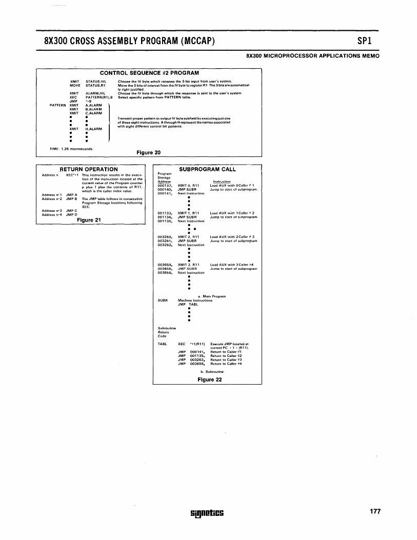
8X300 CROSS ASSEMBLY PROGRAM (MCCAP) SPI 8X300 MICROPROCESSOR APPLICATIONS MEMO
XMIT MOVE
XMIT XEC JMP
PATTERN XMIT XMIT XMIT
• • • XMIT
• • •
CONTROL SEQUENCE #2 PROGRAM STATUS,IVL STATUS,R1
ALARM,IVL PATTERN(R1 ),8 *+9 A,ALARM B,ALARM C,ALARM
• • • H,ALARM
• • •
Choose the IV byte which receives the 3-bit input from user's system. Move the 3 bits of interest from the IV byte to register R1. The 3 bits are automatically right justified. Choose the IV byte through which the response is sent to the user's system. Select specific pattern from PATTERN table.
Transmit proper pattern to output IV bytesubfield by executing just one of these eight instructions. A through H represent the names associated with eight different control bit patterns.
TIME: 1.25 microseconds. Figure 20
~ETURN OPERATION Address n XEC*+1 This instruction results in the execu-
Address n+1 JMP A
tion of the instruction located at the current value of the Program counter p plus 1 plus the contents of R 11, which is the caller index value.
Address n+2 JMP 8 The JMP table follows in consecutive Program Storage locations following SEC.
Address n+3 JMP C Address n+4 JMP D
Figure 21
Program Storage Address 000137, 000140, 000141,
001133, 001134, 001135.
003260, 003261, 003262,
003654, 003655, 003656,
SUBPROGRAM CALL
XMIT 0, R11 JMP SUBR Next Instruction
• • • • XMIT 1, R11 JMP SUBR Next Instruction
• • • • XMIT 2, R11 JMP SUBR Next Instruction
• • • • XMIT 3, R11 JMP SUBR Next Instruction
• • • •
Instruction Load AUX with OCaller # 1 Jump to start of subprogram.
Load AUX with 1 Caller # 2 Jump to start of subprogram.
Load AUX with 2 Caller # 3 Jump to start of subprogram
Load AUX with 3Caller #4 Jump to start of subprogram
a. Main Program SUBR Machine Instructions
Subroutine Return Code
TABL
JMP TABL
• • • •
XEC *+1 (R1 1)
JMP 000141, JMP 001135, JMP 003262, JMP 003656,
Execute JMP located at current PC + 1 + (R1 1). Return to Caller #1 Return to Caller #2 Return to Caller #3 Return to Caller #4
b. Subroutine
Figure 22
!ii!)DotiC!i 177
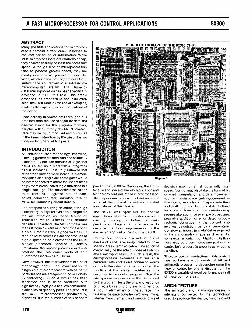
A FAST MICROPROCESSOR FOR CONTROL APPLICATIONS 8X300
ABSTRACT Many possible applications for microprocessors demand a very quick response to requests for action or information. While MOS microprocessors are relatively cheap, they do not generally possess the necessary speed. Although bipolar microprocessors tend to possess greater speed, they are mostly designed as general purpose devices, which means that they are not ideally suited to the requirements of a fast real-time microcomputer system. The Signetics 8X300 microprocessor has been specifically designed to fulfill this role. This article describes the architecture and instruction set of the 8X300 and, by the use of examples, explains the capabilities and applications of the device.
Considerably improved data throughout is obtained from the use of separate data and address buses for the program memory, coupled with extremely flexible I/O control. Data may be input, modified and output all in the same instruction by the use of the two independent, parallel I/O ports.
INTRODUCTION As semiconductor technology improved, allowing greater die area with economically acceptable yield, the amount of logic that could be put on a marketable integrated circuit increased. It naturc;llly followed that rather than provide more individual elementary gates on a single die, these gates would be interconnected to afford the user of these chips more complicated logic functions in a single package. The attractiveness of the more complex integrated circuits compelled semiconductor manufacturers to strive for increasing circuit density.
The prospect of putting an entire, although elementary, computer CPU on a single die focused attention on those fabrication processes which allowed the greatest densities. Therefore, the MOS process was the first to yield an entire microprocessor on a chip. Unfortunately, a price was paid in that the MOS processes did not produce as high a speed of logic element as the usual bipolar processes. Because of density limitations, the bipolar process could only produce the less dense parts of chip microprocessors-the bit slices.
Now, however, the improvements in bipolar technology permit the construction of single chip microprocessors with all of the performance advantages of bipolar Schottky technology. Such a circuit has been fabricated and is being produced with significantly high yield to allow commercial availability of quantity parts. The product is the 8X300 microprocessor produced by Signetics. It is the purpose of this paper to
178
MICROPHOTOGRAPH OF THE 8X300 CHIP fll9
Figure 1
present the 8X300 by discussing the architecture and some of the key fabrication and technology features of the microprocessor. This paper concludes with a brief review of some of the present as well as potential applications of this device.
The 8X300 was optimized for control applications rather than for extensive numerical processing, so before the main presentation begins, it is advisable to describe the basic requirements in the envisaged application field of the 8X300.
Control here applies to a wide variety of areas and is not necessarily limited to those specific areas itemized below. The action of control may be the sole purpose of a standalone microprocessor. In such a task, the microprocessor examines statuses at a particular rate and issues command words or bits to the external circuitry to effect the function of the whole machine as it is described in the control program. Thus, the microprocessor selects specific bits defined by the program, tests the bits, and responds or directs by setting or clearing other bits. Although elementary on the surface, this task may be quite complex involving timing, interval measurement, and various forms of
S!!IDotiCS
decision making, all at potentially high speed. Control may also take the form of bit or word manipulation and data movement such as in data concentrators, communication controllers, disk and tape controllers and similar devices. Here the data destined for storage, transfer or transmission may require alteration (for example bit packing, preamble addition or error detection/correction); consequently the control also involves calculation or data generation. Consider an industrial metal cutter required to form a complex shape as directed by some external data input. Matrix multiplications may be a very necessary part of this controller's process in order to carry out its function.
Thus, we see that controllers in this context may perform a wide variety of bit and arithmetic processing depending upon the type of controller one is discussing. The 8X300 is capable of good performance in all of these control areas.
ARCHITECTURE The architecture of a microprocessor is intimately connected to the technology used to produce the device, for one could
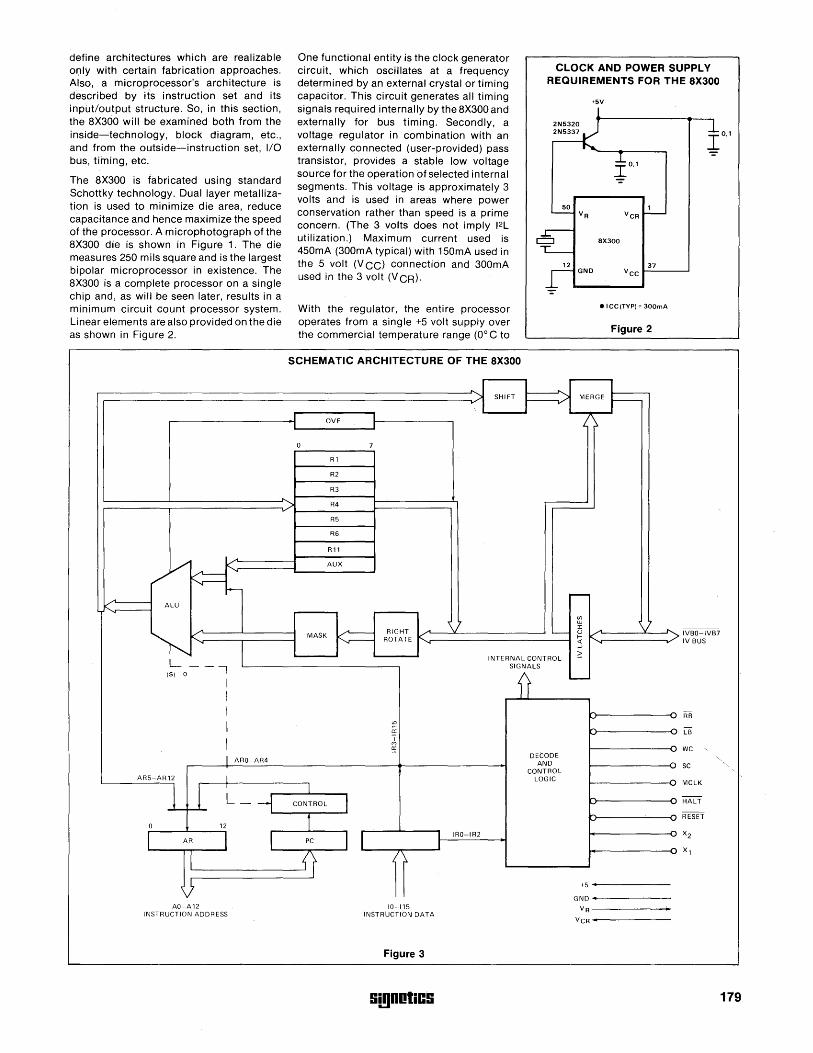
define architectures which are realizable only with certain fabrication approaches. Also, a microprocessor's architecture is described by its instruction set and its input/output structure. So, in this section, the 8X300 will be examined both from the inside-technology, block diagram, etc., and from the outside-instruction set, 1/0 bus, timing, etc.
The 8X300 is fabricated using standard Schottky technology. Dual layer metallization is used to minimize die area, reduce capacitance and hence maximize the speed of the processor. A microphotograph of the 8X300 die is shown in Figure 1. The die measures 250 mils square and is the largest bipolar microprocessor in existence. The 8X300 is a complete processor on a single chip and, as will be seen later, results in a minimum circuit count processor system. Linear elements are also provided on the die as shown in Figure 2.
-"'-
vr==t= ALU
~ K
'"
L __ (51 0 -,
I I I I I I ARO-AR4
AR5-AR12 I
1 1 L_
0 12
l AR I
V AO-A12
INSTRUCTION ADDRESS
l
CLOCK AND POWER SUPPLY REQUIREMENTS FOR THE 8X300
t5V
One functional entity is the clock generator circuit, which oscillates at a frequency determined by an external crystal or timing capacitor. This circuit generates all timing signals required internally by the 8X300 and externally for bus timing. Secondly, a voltage regulator in combination with an externally connected (user-provided) pass transistor, provides a stable low voltage source for the operation of selected internal segments. This voltage is approximately 3 volts and is used in areas where power conservation rather than speed is a prime concern. (The 3 volts does not imply 12L utilization.) Maximum current used is 450mA (300mA typical) with 150mA used in the 5 volt (V CC) connection and 300mA used in the 3 volt (V CR).
.IO.l
With the regulator, the entire processor operates from a single +5 volt supply over the commercial temperature range (0 0 C to
SCHEMATIC ARCHITECTURE OF THE 8X300
... SHIFT
I OVF I I I
0 7
R1
R2
R3
/ R4
R5
R6
Rll
AUX
50
c:::J
12
-=-
I [ I ...
~ RIGHT -"'- V '----MASK K.
I CONTROL I
1 PC J {r
ROTATE
en eI:
~
l It
10-115 INSTRUCTION DATA
Figure 3
!ii!l0otiCii
INTERNAL CONTROL SIGNALS
if
DECODE AND
CONTROL LOGIC
I IRO-IR2
J
*,0.1
V R VCR
8X300
37 GND Vee
• ICC (TVP) = 300mA
Figure 2
MERGE F 1,\
-(/) lJ.J :r:
v-"'- "'- J-,. U l- i<... 5 ... ::::
---r-h ~
r-
r-. ~
r-. ~
~ ,.. r- ~
h
,....
,.... ....,
+5 •
GND •
VR-----
VCR-·------
IVBO-IVB7 IV BUS
RB
LB
WC "
SC
MCLK
HALT
RESET
179
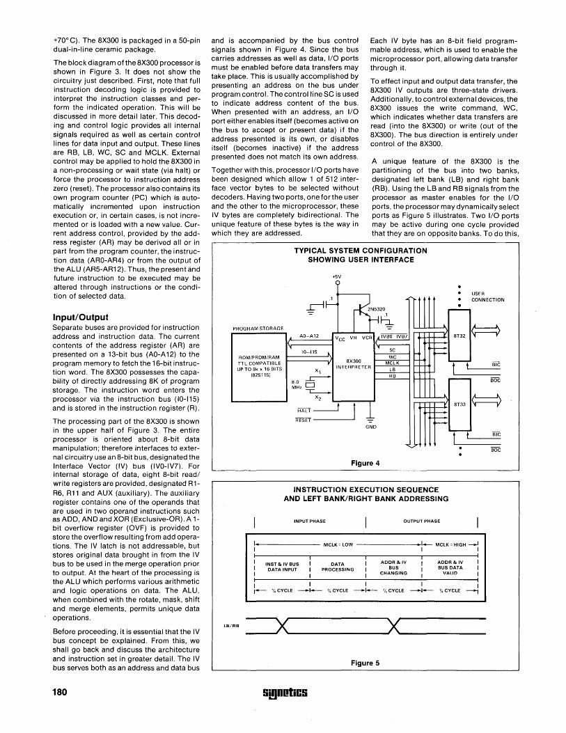
+?O°C). The 8X300 is packaged in a 50-pin dual-in-line ceramic package.
The block diagram of the 8X300 processor is shown in Figure 3. It does not show the circuitry just described. First, 110te that full instruction decoding logic is provided to interpret the instruction classes and perform the indicated operation. This will be discussed in more detail later. This decoding and control logic provides all internai signals required as well as certain control lines for data input and output. These lines are RB, LB, WC, SC and MCLK. External control may be applied to hold the 8X300 in a non-processing or wait state (via halt) or force the processor to instruction address zero (reset). The processor also contains its own program counter (PC) which is automatically incremented upon instruction execution or, in certain cases, is not incremented or is loaded with a new value. Current address control, provided by the address register (AR) may be derived all or in part from the program counter, the instruction data (ARO-AR4) or from the output of the ALU (AR5-AR12). Thus; the present and future instruction to be executed may be altered through instructions or the condition of selected data.
Input/Output Separate buses are provided for instruction address and instruction data. the current contents of the address register (AR) are presented on a 13-bit bus (AO-A 12) to the program memory to fetch the 16-bit instruction word. The 8X300 possesses the capability of directly addressing 8K of program storage. The instruction word enters the processor via the instruction bus (10-115) and is stored in the instruction register (R).
The processing part of the 8X300 is shown in the upper half of Figure 3. The entire processor is oriented about 8-bit data manipulation; therefore interfaces to external circuitry use an 8-bit bus, designated the Interface Vector (IV) bus (IVO-IV?). For internal storage of data, eight 8"'bit read/ write registers are provided, designated R1-R6, R11 and AUX (auxiliary). The auxiliary register contains one of the operands that are used in two operand instructions such as ADD, AND and XOR (Exclusive-OR). A 1-bit overflow register (OVF) is provided to store the overflow resulting from add operations. The IV latch is not addressable, but stores original data brought in from the IV bus to be used in the merge operation prior to output. At the heart of the processing is the ALU which performs various arithmetic and logic operations on data. The ALU, when combined with the rotate, mask, shift and merge elements, permits unique data operations.
Before proceeding, it is essential that the IV bus concept be explained. From this, we shall go back and discuss the architecture and instruction set in greater detail. The IV bus serves both as an address and data bus
180
and is accompanied by the bus control signals shown in Figure 4. Since the bus carries addresses as well as data, I/O ports must be enabled before data transfers may take place. This is usually accomplished by presenting an address on the bus under program control. The control line SC is used to indicate address content of the bus. When presented with an address, an I/O port either enables itself (becomes active on the bus to accept or present data) if the address presented is its own, or disables itself (becomes inactive) if the address presented does not match its own address.
Together with this, processor I/O ports have been designed which allow 1 of 512 interface vector bytes to be selected without decoders. Having two ports, one forthe user and the other to the microprocessor, these IV bytes are completely bidirectional. The unique feature of these bytes is the way in which they are addressed.
Each IV byte has an 8-bit field programmable address, which is used to enable the microprocessor port, allowing data transfer through it.
To effect input and output data transfer, the 8X300 IV outputs are three-state drivers. Additionally, to control external devices, the 8X300 issues the write command, WC, which indicates whether data transfers are read (into the 8X300) or write (out of the 8X300). The bus direction is entirely under control of the 8X300.
A unique feature of the 8X300 is the partitioning of the bus into two banks, designated left bank (LB) and right bank (RB). Using the LB and RB signals from the processor as master enables for the I/O ports, the processor may dynamically select ports as Figure 5 illustrates. Two I/O ports may be active during one cycle provided that they are on opposite banks. To do this,
TYPICAL SYSTEM CONFIGURATION SHOWING USER INTERFACE
+5V q •
r-i~ fF~ ... •
• USER CONNECTION
• ~ -=-
~ PROGRAM STORAGE
L
A AO-A12
VCC VR VCR A IVBO-IVB7 L 8T32
f--'i
10-115 l\ 'i
SC t--~ ~
ROM/PROM/RAM WC '-TTL COMPATIBLE r 8X300 MCLK 1+ -UP TO 8k x 16 BITS Xl
INTERPRETER LB
LB/RB
(82S1151 -.-e-- RB
n ~~z t::J r-r-
L:.--..... ~ X2
HALT~ r 1 1. -RESET -~
GND
.... !r'
Figure 4
INSTRUCTION EXECUTION SEQUENCE AND LEFT BANK/RIGHT BANK ADDRESSING
INPUT PHASE OUTPUT PHASE
~
8T33
ft • •
f.ool .>----~---- MCLK = LOW -------... 1_ MCLK = HIGH ~ 1 1 1 1 1 1 1 INST & IV BUS 1 DATA ADDR & IV ADDR & IV 1 1 DATA INPUT 1 PROCESSING BUS BUS DATA 1 : _ 1 CHANGING VALID:
I. 1 1 1 1 1-- '!. CYCLE --1-- '!. CYCLE --I- '!. CYCLE --1- '!. CYCLE --I
____ x ___________ ~x _________ __ Figure 5
s~nDtiC!i
BIC
I/O ports recognize addresses, data or controls only when enabled by the bank signal to which they are connected. Clearly, the bank partitioning may be considered as a ninth address bit which is alterable by the processor within an instruction. (The 8X300, therefore, has 512 direct I/O port address capability.) A general data operation between two I/O ports could follow the following steps. First, an address is presented to one bank enabling a selected I/O port and disabling all others on that bank. Secondly, another address is presented to the opposite bank effecting a similar selection there. Subsequently, in one instruction cycle, the 8X300 may accept data from one port (on one bank), operate on the data and deposit the result in the other port in the second bank. If the working storage of the registers is not sufficient, additional storage can be added using an I/O port address to add another 256X8 words of RAM . See Figure 6.
In order to fully appreciate the speed of the last operation, accepting data from one port and depositing it on the other, it is necessary to explore the details of the instruction cycle. Each 8X300 operation is executed in one instruction cycle which is subdivided into four quarter cycles. The quarter cycles are shown in Figure 5. The instruction address for an operation is presented at the output during the third quarter of the previous instruction cycle. With a memory of sufficient speed, the instruction is returned and accepted by the processor during the first quarter of the cycle in which that instruction is to be executed. The instruction is decoded and used to direct the operation of the processor throughout the cycle.
For data processing, the instruction cycle may be viewed as having two halves. During the fi rst half of the cycle, data to be processed is brought into the processor and stored in the IV latch. This is accomplished during the first quarter cycle. The next quarter cycle of this first half is used to bring the data through the ALU, thereby processing the data as required by the instruction. The second half cycle is the output phase during which the data is presented to the IV bus and finally clocked into the appropriate I/O port after bus stabilization. The processor issues MCLK for this purpose.
Bank selection during input and output phases is independent, thus data may be input from the right bank and deposited in the left bank or vice-versa, or to and from the same bank if the same IV is used. Bank selection during instruction cycle phases is specified by the instruction. Therefore, the processor may input data from one port, operate on the data and return it to a second port in one instruction cycle time. Remember that instruction fetching is concurrent with data operations. The cycle time is 250ns, making the 8X300 comparable in
WORKING STORAGE (RAM) MAY BE INCLUDED IN THE SYSTEM DESIGN
CONTROL ,'-BUS '-
ADDR LB/- -MCLK
lSI PROGRAM ..
W STORAGE 8X300 R8L
(PROM. ROM) INST J\. ... T
y ,
~
---
II ..
..
WORKING STORAGE
(RAM)
DATA BUS •
-!-
1/0 H PORT 2
~ ....
~--""!-~----
I/O H PORT 1 .... ~
,- ....,.--
LEFT BANK DEVICES
RIGHT BANK DEVICES
Figure 6
speed on a microcycle basis, to bipolar slice systems.
Instruction Set The power of the 8X300 architecture is embodied in the instruction set which controls the ALU, rotate, mask, shift and merge functions to provide for various data operations. Each 16-bit instruction word is subdivided into several fields. The arithmetic and logical instructions follow the format shown in Figure 7. There are eight instruction classes each with variations depending upon the operand specifications. These instructions provide for:
Arithmetic and logic operationsAdd, And and XOR
Data movement-Move and XMIT (transmit)
Context alteration-JMP (unconditional jump), NZT (test and branch on non-zero) and XEC (execute the instruction at the address specified without program counter alteration)
BIT
FORMAT OF ARITHMETIC AND LOGIC INSTRUCTIONS
POSITION 0 1 2 3 7 8 10 11
SOURCE I L I DESTINATION
15
~'~--------~--------~ OP CODE OPERAND(S) SPECIFICATION
L" LENGTH
Figure 7
Si!lDOliCS
The operand fields specify the sou rce of the data as one of the internal registers or from the IV bus as left bank or right bank, and the destination of the data as one ofthe internal registers, left bank or right bank or as left bank or right bank addresses. Additionally, these fields specify the length and position of the data which is to be processed. As an example, see Figure 8.
Before going through an example, some features of this instruction should be explained. The first 3 bits are used for the op-code. The 5 source bits contain two separate information groups: The first 2 bits (3 and 4) define the actual source while the next 3 bits (5, 6 and 7) define the least significant bit of the variable length field of the source. These are represented in the diagram by two digits-the first modulo 4 and the second modulo 8. In the example the first digit being 2 selects left bank I/O (right bank = 3).
The length of the source data field is specified by the length (bits 8,9 and 10). The 5 destination bits are represented by two digits-the first modulo 4 and the second modulo 8, as the source. In Figure 8, the destination is an internal register, specified by the first digit being 0 or 1. The actual register is specified by the value of the second digit. These operand fields control the rotate, mask and shift operations as data proceeds through the microprocessor.
Rather than go through the details of the complete instruction set, it is more instructive to proceed with an example which will serve to illustrate what may be done with a single instruction. What shall be done in this
181
TYPICAL INSTRUCTION
o
OP CODE T SOURCE T "1
11
LENGTH •
15
DESTINATION
• Op Code: 0 (MOVE). 1 (ADD). 2 (AND). 3 (XOR)
• Source: 20 -27. (Left bank). 30 - 37. (Right bank)
• Length: 0 - 7 (L)
• Dest.: 60 - 67 •• 11 •• 17.
• Action: Least Significant L bits of IV source data are right justified and processed by the ALU. The 8-bit result is deposited in the destination register.
SOURCE
DESTINATION 1....----+-__ ---1
Figure 8
example is to select two 1/0 ports, add the contents of the AUX register to a specified segment of the source, merge the result with the original data and deposit the result at the destination.
Suppose the source of the data is in IV port, address 5 on the left bank, and the destination address is contained in internal register R3. Further suppose that the AUX register already contains the required value to be added. First, the 1/0 ports are selected: XMIT 5, IVL (transmit the number 5 to the bus as left bank address). MOVE R3,IVR (move contents of R3 to the bus as a right bank address). The 1/0 ports have now been enabled using two instructions-500ns total thus far. Now perform ADD LB, RB (add left bank to AUX and deposit in right bank port). The add instruction is shown in Figure 9 where the add operand fields specify the selection of bits throughout rotate and length (mask), and after addition specify the position of merge (shift) in the original data. Although the source, length and destination fields shown here are unique to the MOVE, ADD, AND and XOR instructions, the comments made about these fields also apply to the fields of all the other instructions. Port 5 on the left bank is assumed to contain ao-a7
(Figure 10) and the AUX register is assumed to contain bo-b7 . The source field specifies selecting bits starting with a5 and the length field specifies taking 3 bits to the left. Thus, a5, a4 and a3 are masked off and right justified. Note that this requires that only contiguous bits be selected for operation. Next, the selected bits are added to the same length of bits (beginning at the right) from the AUX register.
182
ADD INSTRUCTION TO PERFORM THE ADDITION SHOWN IN
FIGURE 10
OP CODE
ADD
SOURCE I L
LEFT BANK
RIGHT ROTATE
RIGHT BANK
MASK (LENGTH)
Figure 9
DEST
SHIFT
Thus, the sum (a3, a4, a5) + (b5, b6 , b7) is computed producing a 3-bit sum, S1, S2, S3 (and a possible overflow). The destination field of the add instruction then specifies a shift of 1 bit to the left. The shift is made and the 3 bits of the sum are merged with the original source data. Note that the same length specification (3 in the example) applies in source selection, operation and merge functions and is not alterable within one instruction cycle. The destination contains the set of bits shown in Figure 10 after the add operation. Note that the entire set of rotate, mask, add, shift and merge functions took place in one instruction cycle time.
The content of each field can be represented by a set of digits. These digits have a direct relation to the specific operations which the data undergoes as it is directed along the 8X300 internal data paths. The op code for add is 1. This is followed by a two digit source field. The source field is in fact two fields (in this particular case) in which
Smnotics
THE ADD OPERATION
SOURCE I aD I a, I a, I a, I a. I as I a. a, I
~ AUX I x I x I x x I x I bs I b. I b, I
DEST I aD I ~
I
a, I a, I a, I s, I s, s, I a, I "---.r--J
I II
PREVIOUS VALUES OF SOURCE DATA PRESERVED
Figure 10
the first digit, 2, specifies left bank, while the second digit specifies the rotate operation which is to be performed on the incoming data. The L or length field specifies the number of bits to be accepted for ALU operation. This is the mask function specification and selects a quantity of bits counting from the right. The masking operation takes place after the rotate. The destination field, like the source field, specifies the bank or internal register (right bank in this case), and for the bank destination, also specifies the shift operation.
There is one important point to note about the instruction format. Since the fields are easily represented by octal digits and since these digits have a direct relation to the function specified by the field, programming the 8X300 is very easy. Simple mnemonic representation of each of the field specifications, such as ADD for the add function, LB and RB for left bank and right bank and so forth, are easily translated into the octal representation. With this convenience, several hundred lines of program code can be easily generated by hand from the mnemonic representation. Consequently, for small tasks (i.e., less than' 500 instructions), an assembler is not essential for efficient programming. A simple conversion is required to generate the actual program memory content.
The above example is typical of what can be done with the MOVE, ADD, AND and XOR instructions. However, the control functions perform differently and are worthy of further attention. Specifically, the XEC (execute) instruction is powerful in that it may be register or I/O vectored. The XEC instruction temporarily changes the contents of the address register for the one instruction cycle following the XEC while allowing sub-
sequent control to be resumed through the program counter. In this light, XEC may be viewed as calling a single instruction subroutine. The XEC instruction performs the vectoring by concatenating the higher order program counter contents with a number determined, in part, by the contents of one of the internal registers or by the content Gf an I/O port. Thus, the XEC instruction may be used to sequence through a list where the list counter is an internal register, or it may be used to branch to a specific service routine based on some external status reflected in a selected I/O port.
APPLICATIONS The 8X300 may be exploited in a variety of applications where high speed is required and where the architecture fits the particular requirement. The 8X300 may serve in disk controllers, communications data concentrators and demultiplexers, tape controllers, industrial process controllers, video controllers including entertainment and games, as well as CRT/keyboard terminals, plus a variety of other applications. Principally, the 8X300 affords its greatest service to the user in high speed, relatively sophisticated systems. For example, a low speed MOS processor might be used to control a CRT display and do so economically. However, add the requirement to do data processing for, say, graphics or color display, then the 8X300 becomes increasingly attractive. With 8-bit parallel to serial conversion, the 8X300 may easily process data and directly produce video for alphanumeric display. Generally, one may conclude that the 8X300 serves well where the control processor is required to be in the data path. In controlling computer peripherals, one alternative is to use a single 8X300 processor to control a number of peripherals, as opposed to having one lower speed, less costly processor with separate memory and auxiliary circuits in each peripheral.
Economically, the 8X300 is certainly competitive with the bit slice approach. For those who need the performance, the 8X300 affords a complete, single chip processor at a power consumption of only 1.5 watts in contrast to three to four chips for a bit slice equivalent using nearly 5 watts.
The typical system configuration for the 8X300 is shown in Figure 4. The 8X300 interfaces to the external world through a convenient number of I/O ports connected to the IV bus. Program storage is provided by a suitable ROM or PROM, but RAM could be used here also depending upon the user's application. However, in the more common control applications, the function of the processor is dedicated and, consequently, there is no need to have alterable program storage. This reasoning is also evident in the 8X300 architecture, as exem-
plified in Figure 4. It is clear that there is no direct connection between the program store and the I/O system, as opposed to other microprocessors (the MOS microprocessor in particular) in which instructions are fetched over the same bus on wh ich data and I/O transfers take place.
Figure 4 also emphasizes the compact nature of the processor system. Note that the CPU and program store are realized in as few as three packages (e.g. 8X300 with two 82S115 chips). I/O ports are added as required for the particular system configuration.
Connections to the IV bus are not restricted to the 8T32 type of addressable bidirectional I/O port. Depending upon requirements, a number of devices may be employed. Working storage in the form of RAM may be interfaced directly to the IV bus with an 8T31 or other suitable device used as an address latch. This affords the user temporary storage for data and status information. ROM may also be provided in order to access fixed constants for use by the processor. Examples of such ROM include sine function look-up tables, coordinate translation constants, sensor linearization curves, etc.
Some users have objected to the overhead cost in addressing I/O ports prior to an operation. As in the example used in this paper, 500ns (two instructions) were taken up in selecting I/O ports prior to the major data operation. This is acceptable if ports continue to be accessed for a number of times and thereby reduce the addressing overhead. However, for those who see this as a limitation, there is a convenient alternative. The instruction memory may be extended such that an extra field appears as an additional bus which is applied to each I/O port. Port selection (addressing) would then be done upon instruction fetch. No latch addressable I/O ports would be used, but the normal active-on-address-decode scheme would be employed. The address field may be as wide as required to serve all system I/O ports and if necessary memory. Bus left bank and right bank partitioning would still be used, so the address field would contain two addresses, one for each bank. With this scheme, an entire operation such as described earlier, including the selection of I/O ports, could be accomplished in 250ns.
Gi!lDOliCG 183

184 Gi!lDOliCG
CIIAPTER 5 DEYEIOpmEnT SYSTEmS
AnD PROGRAmS
S!!IDOliCS 185

186 !ii!lDotiC!i
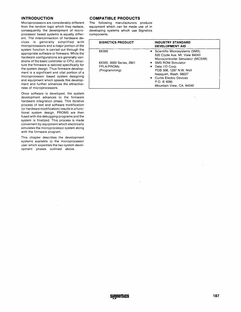
INTRODUCTION Microprocessors are considerably different from the random logic which they replace, consequently the development of microprocessor based systems is equally different. The interconnection of hardware devices is generally simplified with microprocessors and a major portion of the system function is carried out through the appropriate software or firmware. While the hardware configurations are generally variations of the basic controller or CPU, structure the firmware is tailored specifically for the system design. Thus firmware development is a significant and vital portion of a microprocessor based system designing and equipment which speeds this development and further enhances the attractiveness of microprocessors.
Once software is developed, the system development advances to the firmware hardware integration phase. This iterative process of test and software modification (or hardware modification) results in a functional system design. PROMS are then fused with the debugging programs and the system is finalized. This process is made convenient by equipmentwhich electrically simulates the microprocessor system along with the firmware program.
This chapter describes the development systems available to the microprocessor user which expedites the two system development phases outlined above.
COMPATIBLE PRODUCTS The following manufacturers produce equipment which can be made use of in developing systems which use Signetics components.
SIGNETICS PRODUCT
8X300
8X300, 3000 Series, 2901 FPLA/PROMs (Programming)
Si!)DotiCS
INDUSTRY STANDARD DEVELOPMENT AID
• Scientific Microsystems (SMS) 520 Clyde Ave. Mt. View 94043 Microcontroller Simulator (MCSIM)
• SMS ROM Simulator • Data 1/0 Corp.
POB 308, 1297 N.W. Mall Issaquah, Wash. 98027
• Curtis Electro Devices P.O. B 4090 Mountain View, CA. 94040
187

188 Gi!lDOliCG

!ii!lDOliC!i
CIIAPTIR6 MiliTARY
189

190 !ii!)DotiC!i
The Signetics Mil 38510/883 Program is organized to provide a broad selection of processing options, structured around the most commonly requested customer flows. The program is designed to provide our customers:
• Standard processing flows to help minimize the need for custom specs.
• Cost savings realized by using standard processing flows in lieu of custom flows.
• Better delivery lead times by minimizing spec negotiation time, plus allows customers to buy product off-the-shelf or in various stages of production rather than waiting for devices started specifically to custom specs.
The following explains the different processing options available to you. Special device marking clearly distinguishes the type of screening performed.
JAN QUALIFIED JAN Qualified product i~ designed to give you the optimum in quality and reliability. The JAN processing level is offered as the result of the government's product standardization programs, and is monitored by the Defense Electronic Supply Center (DESC), through the use of industry-wide procedures and specifications.
JAN Qualified products are manufactured, processed and tested in a government certified facility to Mil-M 38510, and appropriate device slash sheet specifications. Design documentation, lot sampling plans, electrical test data and qualification data for each specific part type has been approved by the Defense Electronic Supply Center (DESC) and products appear on the DESC Qualified Products List (QPL-38510).
Group B testing, per Mil-Std-883 Method 5005, is performed on each six weeks of production on each slash sheet for each package type. Group C, per Mil-Std-883 Method 5005, is performed every ninety days for each microcircuit group. Group D testing, per Mil-Std-883 Method 5005, is performed every six months for each package type.
In addition to the common specs used throughout the industry for processing and testing, JAN Qualified products also possess a requirement for a standard marking to be used throughout the IC industry.
JAN PROCESSING This option is extremely useful when the reliability and screening of a JAN device is required, however, Signetics is not listed on the QPL forthe product needed. Processing is performed to Mil-Std-883 Method 5004, and product is 100% electrically tested to the appropriate JAN slash sheet.
Group B, C and D data for JAN processed and the other military processing levels which follow, consists of Group Band D testing performed per Mil-Std-883 Method 5005, every six months minimum by package type and Group C per Mil-Std-883 Method 5005, is run every ninety days on each microcircuit group.
JAN REL Processing to this option is ideal when no JAN slash sheets are released on devices required. Product is processed to Mil-Std-883 Method 5004, and is 100% electrically tested to industry data sheets. (Specific parameters required by a customer may also be included.)
/8838 This is a lower priced version ofthe JAN Rei option described above. Processing is identical with the only exceptions being the dc electrical testing over the temperature range and ac electrical testing at room temperature are performed as a part of Group A instead of 100%.
MIL TEMP If you need a Military temp. range device, but do not require all the high reliability screening performed in the other processing options, our Mil-Temp. product is ideal. Mil-Temp. parts are the standard full MilTemperature range product guaranteed to a 1 % AQL to the Signetics data sheet parameters.
S!!IDotiCS
MILITARY GENERIC DATA Signetics has a new program for those customers who require qualification data on their products. This program allows our customers to obtain reliability information without the necessity of running Groups B, C and D inspections for their particular purchase order. It provides for the customer something that has not been readily available before in the semiconductor industry in that all Military Generic Data is controlled and audited by both Government Inspection and Quality Assurance.
Signetics Military Generic Data is generated by the Military Products Division. The data is compiled from 1) JAN qualification lots, and 2) Data generated by qualification lots run for other reliability programs.
A Military Generic family is defined as consisting of die function and package type families.
A Generic die function lot qualifies a ninety day manufacturing period and a representative package type qualifies a one hundred and eight day manufacturing period.
Military Generic Data • Allows our customers to qualify Signet
ics products based on existing qualification data performed at Signetics.
• Allows our customers to reduce costs and improve deliveries.
• Provides assurance that all Signetics die function families and packages meet JAN and customer reliability requirements.
• Provides and attributes summary to the customer backed by lot identity and traceability.
Generic Quality Conformance Data is supplied upon customer request in a format conforming to either Notice 2 (March 1, 1976) or Notice 1 (February 5,1975) of MilStd-883A. Testing to either notice is considered equivalent, since only the test frequency has been altered. Table 2 provides the definition and qualifying manufacturing periods as outlined in Notice 1 and Notice 2 of Mil-Std-883A.
191
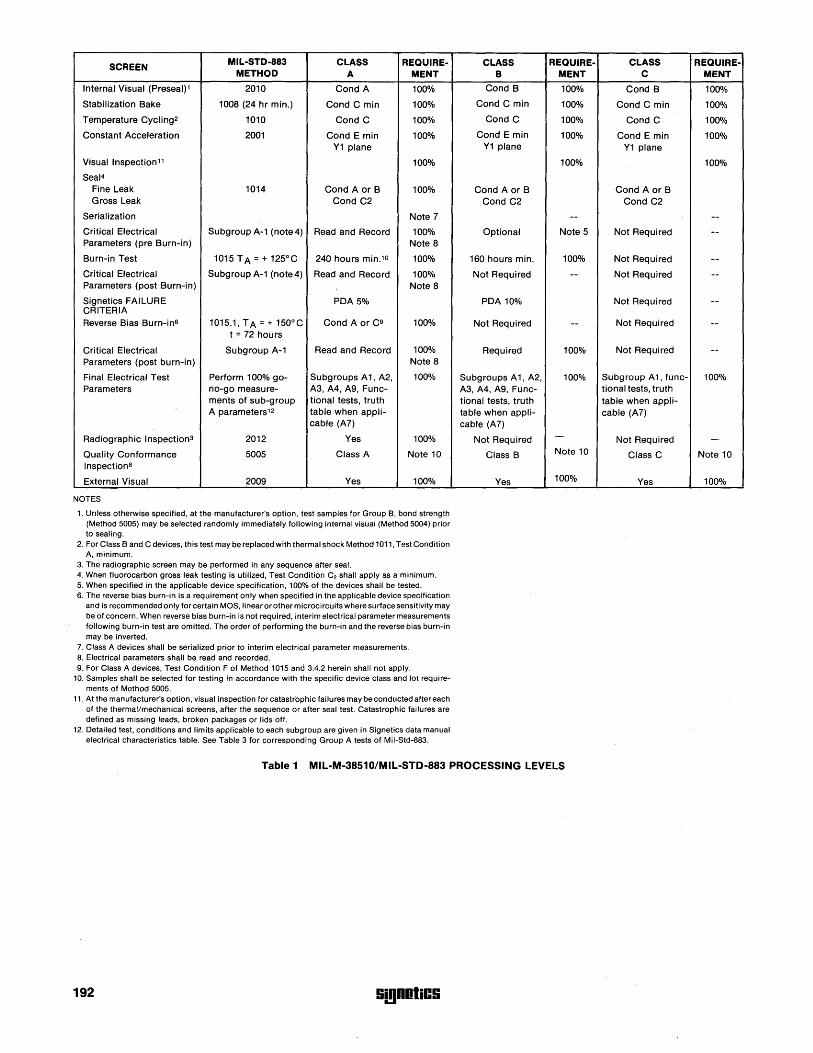
SCREEN MIL-STD-883 CLASS REQUIRE-METHOD A MENT
Internal Visual (Preseal)1 2010 Cond A 100%
Stabilization Bake 1008 (24 hr min.) Cond C min 100%
Temperature Cycling2 1010 Cond C 100%
Constant Acceleration 2001 Cond E min 100% Y1 plane
Visual Inspection11 100%
Seal4
Fine Leak 1014 Cond A or B 100% Gross Leak Cond C2
Serialization Note 7
Critical Electrical Subgroup A-1 (note4) Read and Record 100% Parameters (pre Burn-in) Note 8
Burn-in Test 1015 T A = + 125°C 240 hours min.1O 100%
Critical Electrical Subgroup A-1 (note4) Read and Reco.rd 100% Parameters (post Burn-in) Note 8
Signetics FAILURE PDA5% CRITERIA Reverse Bias Burn-in6 1015.1, T A = + 150°C Cond A or C9 100%
t = 72 hours
Critical Electrical Subgroup A-1 Read and Record 100% Parameters (post burn-in) Note 8
Final Electrical Test Perform 100% go-:- Subgroups A 1, A2, 100% Parameters no-go measure- A3, A4, A9, Func-
ments of sub-group tional tests, truth A parameters12 table when appli-
cable (A7)
Radiographic Inspection3 2012 Yes 100%
Quality Conformance 5005 Class A Note 10 InspectionS
External Visual 2009 Yes 100%
NOTES
1. Unless otherwise specified, at the manufacturer's option, test samples for Group B, bond strength (Method 5005) may be selected randomly immediately following internal visual (Method 5004) prior to sealing.
2. For Class Band C devices, this test maybe replaced with thermal shock Method 1011, TestCondition A, minimum.
3. The radiographic screen may be performed in any sequence after seal. 4. When fluorocarbon gross leak testing is utilized, Test Condition C2 shall apply as a minimum. 5. When specified in the applicable device specification, 100% of the devices shall be tested. 6. The reverse bias burn-in is a requirement only when specified in the applicable device specification
and is recommended only for certain MOS, linear orother microcircuits where surface sensitivity may be of concern. When reverse bias burn-in is not required, interim electrical parameter measurements following burn-in test are omitted. The order of performing the burn-in and the reverse bias burn-in may be inverted.
7. Class A devices shall be serialized prior to interim electrical parameter measurements. 8. Electrical parameters shall be read and recorded. 9. For Class A devices, Test Condition F of Method 1015 and 3.4.2 herein shall not apply.
10. Samples shall be selected for testing in accordance with the specific device class and lot requirements of Method 5005.
11. At the manufacturer's option, visual inspection for catastrophic failures may be conducted after each of the thermal/mechanical screens, after the sequence or after seal test. Catastrophic failures are defined as missing leads, broken packages or lids off.
12. Detailed test, conditions and limits applicable to each subgroup are given in Signetics data manual electrical characteristics table. See Table 3 for corresponding Group A tests of Mil-Std-883.
CLASS REQUIRE-B MENT
Cond B 100%
Cond C min 100%
Cond C 100%
Cond E min 100% Y1 plane
100%
Cond A or B Cond C2
--Optional Note 5
160 hours min. 100%
Not Required --
PDA10%
Not Required --
Required 100%
Subgroups A 1, A2, 100% A3, A4, A9, Func-tiona I tests, truth table when appli-cable (A7)
Not Required -
Class B Note 10
Yes 100%
Table 1 MIL-M-38510/MIL-STD-883 PROCESSING LEVELS
192 !i(gnotiC!i
CLASS REQUIRE-C MENT
Cond B 100%
Cond C min 100%
Cond C 100%
Cond E min 100% Y1 plane
100%
Cond A or B Cond C2
--Not Required --
Not Required --Not Required --
Not Required --
Not Required --
Not Required --
Subgroup A 1, func- 100% tional tests, truth table when appli-cable (A7)
Not Required -
Class C Note 10
Yes 100%
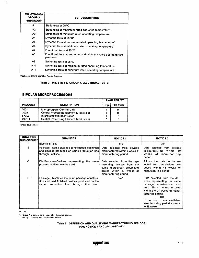
MIL-STD-883A GROUP A TEST DESCRIPTION
SUBGROUP
A1 Static tests at 25°C
A2 Static tests at maximum rated operating temperature
A3 Static tests at minimum rated operating temperature
A4 Dynamic tests at 25°C*
A5 Dynamic tests at maximum rated operating temperature*
A6 Dynamic tests at minimum rated operating temperature* A7 Functional tests at 25° C
A8 Functional tests at maximum and minimum rated operating tem-peratures
A9 Switching tests at 25°C
A10 Switching tests at maximum rated operating temperature A11 SWitching tests at minimum rated operating temperature
·Applicable only to Signetics Analog Products
Table 3 MIL-STD-883 GROUP A ELECTRICAL TESTS
BIPOLAR MICROPROCESSORS
PRODUCT
3001 3002 8X300 2901-1
·Under development
QUALIFIED SUB-GROUPS
NOTES
A
B
C
o
DESCRIPTION
Microprogram Control Unit Central Processing Element (2-bit slice) Interpreter /M icrocontroller Central Processing Element (4-bit slice)
QUALIFIES
Electrical Test
Package-Same package construction lead finish and devices produced on same production line through final seal.
Die/Process-Devices representing the same process families may be used.
Package-Qualifies the same package construction and lead finished devices produced on the same production line through final seal.
1. Group A is performed on each lot of Signetics devices. 2. Group D not offered in Mil-Std-883 Notice 1.
AVAILABILITY
Dip Flat Pack
I R I R I * * *
NOTICE 1
n/a1
Data selected from devices manufactured within 6 weeks of manufacturing period.
Data selected from the representing devices from the same microcircuit group and sealed within 12 weeks of manufacturing period.
n/a2
NOTICE 2
n/a1
Data selected from devices manufactured within 24 weeks of manufacturing period.
Allows the data to be selected from the devices produced within 48 weeks of manufacturing period.
Data selected from the devices representing the same package construction and lead finish manufactured within the 24 weeks of manufacturing period.
OR If no such data available,manufacturing period extends to 48 weeks.
Table 2 DEFINITION AND QUALIFYING MANUFACTURING PERIODS FOR NOTICE 1 AND 2 MIL-STD-883
9i!110liC9 193
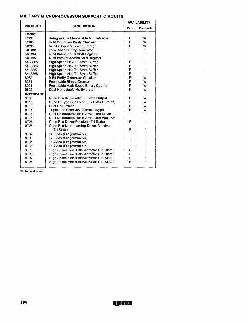
MILITARY MICROPROCESSOR SUPPORT CIRCUITS AVAILABILITY
PRODUCT DESCRIPTION Dip Fla'pack
LOGIC 54123 Retriggerable Monostable Multivibrator F W 54180 8-Bit Odd/Even Parity Checker F W 54298 Quad 2-lnput Mux with Storage F W 54S182 Look-Ahead Carry Generator * *
54S194 4-Bit Bidirectional Shift Register * *
54S195 4-Bit Parallel Access Shift Register * *
54LS365 High Speed Hex Tri-State Buffer F *
54LS366 High Speed Hex Tri-State Buffer F *
54LS367 High Speed Hex Tri-State Buffer F *
54LS368 High Speed Hex Tri-State Buffer F *
8262 9-Bit Parity Generator Checker F W 8281 Presettable Binary Counter F W 8291 Presettable High Speed Binary Counter F W 9602 Dual Monostable Multivibrator F W
INTERFACE 8T09 Quad Bus Driver with Tri-State Output F W 8T10 Quad D-Type Bus Latch (Tri-State Outputs) F W 8T13 Dual Line Driver F W 8T14 Triple Line Receiver/Schmitt Trigger F W 8T15 Dual Communication EIA/Mil Line Driver * *
8T16 Dual Communication EIA/Mil Line Receiver * *
8T26 Quad Bus Driver/Receiver (Tri-State) F *
8T28 Quad Bus Non-Inverting Driver/Receiver (Tri-State) F *
8T32 IV Bytes (Programmable) I * 8T33 IV Bytes (Programmable) I * 8T34 IV Bytes (Programmable) I * 8T35 IV Bytes ,(Programmable) I * 8T95 High Speed Hex Buffer/Inverter (Tri-State) F * 8T96 High Speed Hex Buffer/Inverter (Tri-State) F * 8T97 High Speed Hex Buffer/Inverter (Tri-State) F * 8T98 High Speed Hex Buffer/Inverter (Tri-State) F *
·Under development
194 9i!1DOliC9
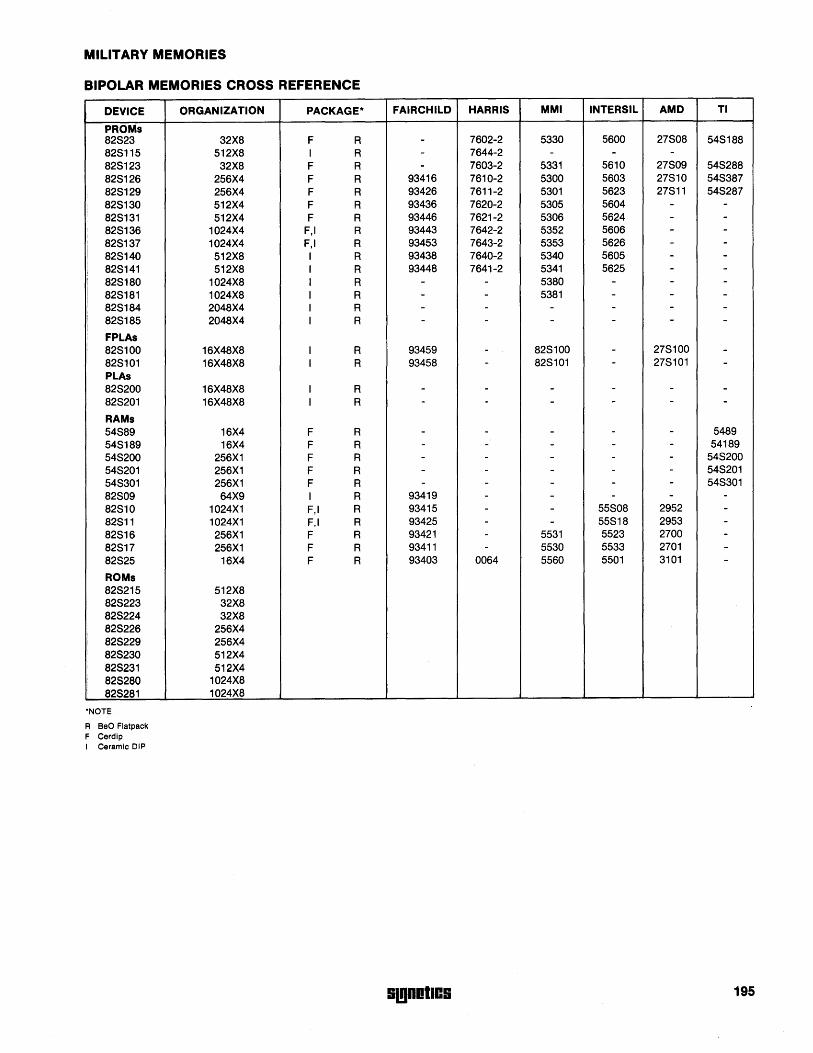
MILITARY MEMORIES
BIPOLAR MEMORIES CROSS REFERENCE
DEVICE
PROMs 82823 828115 828123 828126 828129 828130 828131
I 828136 i
828137 828140 828141 828180 828181 828184 828185 FPLAs 828100 828101 PLAs 828200 828201
RAMs 54889 548189 548200 548201 548301 82809 82810 82811 82816 82817 82825
ROMs 828215 828223 828224 828226 828229 828230
I 828231 828280 828281
"NOTE
R BeO Flatpack F Cerdip I Ceramic DIP
ORGANIZATION PACKAGE*
32X8 F R 512X8 I R
32X8 F R 256X4 F R 256X4 F R 512X4 F R 512X4 F R
1024X4 F,I R 1024X4 F,I R 512X8 I R 512X8 I R
1024X8 I R 1024X8 I R 2048X4 I R 2048X4 I R
16X48X8 I R 16X48X8 I R
16X48X8 I R 16X48X8 I R
16X4 F R 16X4 F R
256X1 F R 256X1 F R 256X1 F R 64X9 I R
1024X1 F,I R 1024X1 F,I R
256X1 F R 256X1 F R
16X4 F R
512X8 32X8 32X8
256X4 256X4 512X4 512X4
1024X8 1024X8
FAIRCHILD
---
93416 93426 93436 93446 93443 93453 93438 93448
----
93459 93458
--
-----
93419 93415 93425 93421 93411 93403
lii!lDOliCIi
HARRIS MMI INTERSIL AMD TI
7602-2 5330 5600 27808 548188 7644-2 - - -7603-2 5331 5610 27809 548288 7610-2 5300 5603 27810 548387 7611-2 5301 5623 27811 548287 7620-2 5305 5604 - -7621-2 5306 5624 - -7642-2 5352 5606 - -7643-2 5353 5626 - -7640-2 5340 5605 - -7641-2 5341 5625 - -
- 5380 - - -- 5381 - - -- - - - -- - - - -
- 828100 - 278100 -- 828101 - 278101 -
- - - - -- - - - -
- - - - 5489 - - - - 54189 - - - - 548200 - - - - 548201 - - - - 548301 - - - - -- - 55808 2952 -- - 55818 2953 -- 5531 5523 2700 -- 5530 5533 2701 -
0064 5560 5501 3101 -
195
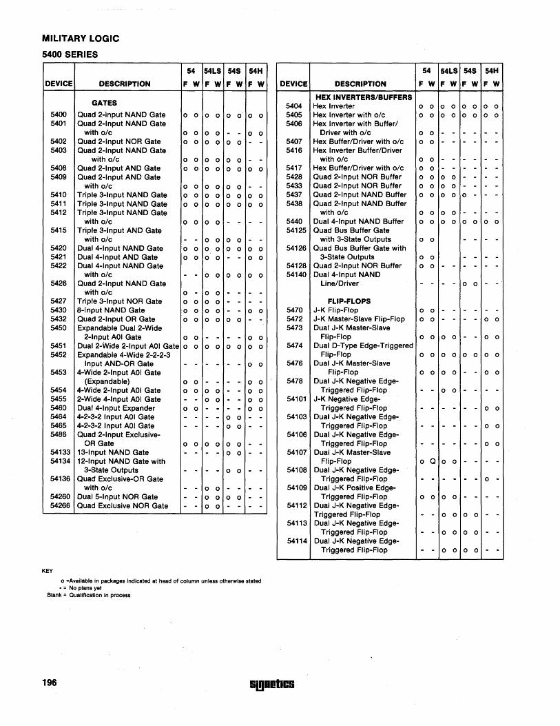
MILITARY LOGIC
5400 SERIES
DEVICE DESCRIPTION
GATES
5400 Quad 2-input NAND Gate 5401 Quad 2-lnput NAND Gate
with o/c 5402 Quad 2-lnput NOR Gate 5403 Quad 2-lnput NAND Gate
with o/c 5408 Quad 2-lnput AND Gate 5409 Quad 2-lnput AND Gate
with o/c 5410 Triple 3-lnput NAND Gate 5411 Triple 3-lnput NAND Gate 5412 Triple 3-lnput NAND Gate
with o/c 5415 Triple 3-lnput AND Gate
with o/c 5420 Dual4-lnput NAND Gate 5421 Dual4-lnput AND Gate 5422 Dual 4-lnput NAND Gate
with o/c 5426 Quad 2-lnput NAND Gate
with o/c 5427 Triple 3-lnput NOR Gate 5430 8-lnput NAND Gate 5432 Quad 2-lnput OR Gate 5450 Expandable Dual 2-Wide
54
F W
0 0
0 0
0 0
0 0
0 0
0 0
0 0
0 0
0 0
- -0 0
0 0
- -
0 -0 0
0 0
0 0
2-lnput AOI Gate 0 0
5451 Dual 2-'Nide 2-lnput AOI Gate 0 0
5452 Expandable 4-Wide 2-2-2-3 Input AND-OR Gate - -
5453 4-Wide 2-lnput AOI Gate (Expandable) 0 0
5454 4-Wide 2-lnput AOI Gate 0 0
5455 2-Wide 4-lnput AOI Gate - -5460 Dual 4-lnput Expander 0 0 5464 4-2-3-2 Input AOI Gate - -5465 4-2-3-2 Input AOI Gate - -5486 Quad 2-lnput Exclusive-
OR Gate 0 0
54133 13-lnput NAND Gate - -54134 12-lnput NAND Gate with
3-State Outputs - -54136 Quad Exclusive-OR Gate
with o/c - -54260 Dual 5-lnput NOR Gate - -54266 Quad Exclusive NOR Gate - -
KEY
54LS 54S 54H
F W F W F W
0 0 0 0 0 0
0 0 - - 0 0
0 0 0 0 - -
0 0 0 0 - -0 0 0 0 0 0
0 0 0 0 - -0 0 0 0 0 0
0 0 0 0 0 0
0 0 - - - -
0 0 0 0 - -0 0 0 0 0 0
0 0 - - 0 0
0 0 0 0 0 0
0 0 - - - -0 0 - - - -0 0 - - 0 0
0 0 0 0 - -
- - - - 0 0
0 0 0 0 0 0
- - - - 0 0
- - - - 0 0
0 0 - - 0 0
0 0 - - 0 0
- - - - 0 0
- - 0 0 - -- - 0 0 - -
0 0 0 0 - -- - 0 0 - -
- - 0 0 - -0 0 - - - -0 0 0 0 - -0 0 - - - -
o =Available in packages indicated at head of column unless otherwise stated - = No plans yet
Blank = Qualification in process
DEVICE
5404 5405 5406
5407 5416
5417 5428 5433 5437 5438
5440 54125
54126
54128 54140
5470 5472 5473
5474
5476
5478
54101
54103
54106
54107
54108
54109
54112
54113
54114
196 lii!llOliCIi
DESCRIPTION
HEXINVERTERS/BUFFERS Hex Inverter Hex Inverter with o/c Hex Inverter with Bufferl
Driver with o/c Hex BufferlDriver with o/c Hex Inverter BufferlDriver
with o/c Hex BufferlDriver with o/c Quad 2-lnput NOR Buffer Quad 2-lnput NOR Buffer Quad 2-lnput NAND Buffer Quad 2-lnput NAND Buffer
with o/c Dual 4-lnput NAND Buffer Quad Bus Buffer Gate
with 3-State Outputs Quad Bus Buffer Gate with
3-State Outputs Quad 2-lnput NOR Buffer Dual 4-lnput NAND
Line/Driver
FLIP-FLOPS J-K Flip-Flop J-K Master-Slave Flip-Flop Dual J-K Master-Slave
Flip-Flop Dual D-Type Edge-Triggered
Flip-Flop Dual J-K Master-Slave
Flip-Flop Dual J-K Negative Edge-
Triggered Flip-Flop J-K Negative Edge-
Triggered Flip-Flop Dual J-K Negative Edge-
Triggered Flip-Flop Dual J-K Negative Edge-
Triggered Flip-Flop Dual J-K Master-Slave
Flip-Flop Dual J-K Negative Edge-
Triggered Flip-Flop Dual J-K Positive Edge-
Triggered Flip-Flop Dual J-K Negative Edge-Triggered Flip-Flop Dual J-K Negative Edge-
Triggered Flip-Flop Dual J-K Negative Edge-
Triggered Flip-Flop
54 54LS 54S 54H
F W F W F W F W
0 0 0 0 0 0 0 0
0 0 0 0 0 0 0 0
0 0 - - - - - -0 0 - - - - - -
0 0 - - - - - -0 0 - - - - - -0 0 0 0 - - - -0 0 0 0 - - - -0 0 0 0 0 - - -
0 0 0 0 - - - -0 0 0 0 0 0 0 0
0 0 - - - -0 0 - - - -0 0 - - - - - -
- - - - 0 0 - -
0 0 - - - - - -0 0 - - - - 0 0
0 0 0 0 - - 0 0
0 0 0 0 0 0 0 0
0 0 0 0 - - 0 0
- - 0 0 - - - -
- - - - - - 0 0
- - - - - - 0 0
- - - - - - 0 0
o Q 0 0 - - - -
- - - - - - 0 -
0 0 0 0 - - - -
- - 0 0 0 0 - -
- - 0 0 0 0 - -
- - 0 0 0 0 - -
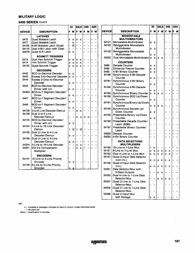
MILITARY LOGIC
5400 SERIES Cont'd
DEVICE DESCRIPTION
LATCHES 5475 Quad Bistable Latch 5477 Quad Bistable Latch 54100 4-Bit Bistable Latch (Dual) 54116 Dual 4-Bit Latch with Clear 54279 Quad S-R Latch
SCHMITT TRIGGERS 5413 Dual Hex Schmitt Trigger 5414 Hex Schmitt Trigger 54132 Quad Schmitt Trigger
DECODERS 5442 BCD-to-Decimal Decoder
54
F W
0 0
- 0
I Q I -0 0
0 0
.0 0
0 0
0 0
5443 Excess 3-to-Decimal Decoder 0 0
5444 Excess 3-Gray-to-Decimal Decoder 0 0
5445 BCD-to-Decimal Decoderl Driver with o/c 0 0
5446A BCD-to-7 Segment Decoderl Driver 0 0
5447 BCD-to-7 Segment Decoderl Driver 0 0
5448 BCD-to-7 Segment Decoderl Driver 0 0
54138 3-to-8 Line Decoder/Demux - -54139 Dual 2-to-4 Line
Decoder/Demux - -54145 BCD-to-Decimal Decoderl
Driver with o/c 0 0
54154 4-Line to 16-Line Decoderl Demux I Q
54155 Dual 2-Llne to 4-Line Decoder/Demux 0 0
54156 Dual 2-Line to 4-Line Decoder/Demux 0 0
54254 4-Line to 16-Line Decoder - -54261 2X4 2's Complement- - -
Multiplier
ENCODERS' 54147 10-Line to 4-Line Priority
Encoder 0 0
54148 8-Line to 3-Line Priority Encoder o 0
KEY
54LS 54S 54H
F W F W F W
0 0 - - - -- - - - - -- - - - - -- - - - - -
- - - -
0 0 - - - -0 0 - - - -0 0 - - - -
- - - -- - - - - -
- - - - - -
- - - - - -
- - - - - -
- - - - - -
- - - - - -0 0 - - - -
0 0 0 0 - -
- - - -
I Q - - - -
- - - - - -
- - - - - -0 0 - - - -0 0 - - - -
- - - - - -
- - - - - -
o = Available in packages indicated at head of column unless otherwise stated - = No plans yet
Blank = Qualification in process
DEVICE
54121 54122
54123
54222
5490 5492 5493 54160
54161
54162
54163 54190
54191
54192
54193
54196
54197
54290 54293
54150 54151 54153 54157
54158
54251
54253
54257
54258
54298
Gi!lnOliCG
54 54LS 54S 54H
DESCRIPTION F W F W F W F W
MONOSTABLE MUL TIVIBRATORS
Monostable-M u Itivi brator 0 0 - - - -Retriggerable Monostable
Multivibrator 0 0 - - - -Retriggerable Monostable
Multivibrator 0 0 - - - -Dual Monostable Multivibrator 0 0 0 0 - - - -
COUNTERS Decade Counter 0 0 - - - -Divide-by-Twelve Counter 0 0 - - - -4-Bit Binary Counter 0 0 - - - -Synchronous 4-Bit Decade
Counter 0 0 - - - - - -Synchronous 4-Bit Binary
Counter 0 0 - - - -Synchronous 4-Bit Decade
Counter 0 0 - - - - - -Synchronous Binary Counter 0 0 0 0 - - - -Synchronous BCD Up/Down
Counter 0 0 - - - -Synchronous Binary Up/Down
Counter 0 0 0 0 - - - -Synchronous Decade Upl
Down Counter 0 0 - - - -Presettable Binary Up/Down
Counter 0 0 - - - -Presettable Decade Counterl
Latch (8290) - - - - - -Presettable Binary Counterl
Latch - - - - - -Decade Counter - - - - - -4-Bit Binary Counter - - - - - -
DATA SELECTORSI MUL TIPLEXERS
16-Line to 1-Line Mux I 0 - - - - - -8-Line to 1-Line Mux 0 0 0 0 0 0 - -Dual 4-Line to 1-Line Mux 0 0 0 0 0 0 - -Quad 2-lnput Data Selector
(non-inv.) 0 0 0 0 0 0 - -Quad 2-lnput Data Selector
(inv.) 0 0 0 0 0 0 - -Data Selector/Mux with
3-State Outputs - - 0 0 - - - -Dual 4-Line to 1-Line Data
Selector/Mux - - 0 0 0 0 - -Quad 2-Line to 1-Line Data
Selector/Mux - - - - - -Quad 2-Line to 1-Line Data
Selector/Mux - - - - - -Quad 2-lnput Mux
with Storage 0 0 - - - - - -
197
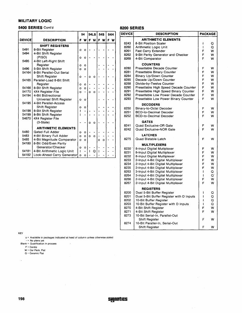
MILITARY LOGIC
5400 SERIES Cont'd
DEVICE DESCRIPTION
SHIFT REGISTERS 5491 8-Bit Register 5494 4-Bit Shift Register
(PISO) 5495 4-Bit Left-Right Shift
Register 5496 5-Bit Shift Register 54164 8-Bit Parallel-Out Serial
Shift Register 54165 Parallel-Load 8-Bit Shift
Register 54166 8-Bit Shift Register 54170 4X4 Register File 54194 4-Bit Bidirectional
Universal Shift Register 54195 4-Bit Parallel-Access
Shift Register 54198 8-Bit Shift Register 54199 8-Bit Shift Register 54670 4X4 Register File
(3-State)
ARITHMETIC ELEMENTS 5480 Gated Full Adder 5483 4-Bit Binary Full Adder 5485 4-Bit Magnitude Comparator 54180 8-Bit Odd/Even Parity
Generator/Checker 54181 4-Bit Arithmetic Logic Unit 54182 Look-Ahead Carry Generator
KEY
54 54LS 54S 54H
F W F VI F W F W
0 0 - - - - - -0 0 - - - - - -
0 0 - - - -0 0 - - - -0 - 0 0 - - - -
0 0 - - - - - -0 0 - - - - - -0 - 0 0 - - - -
0 0 - - - -
0 0 - - - -I - - - - - - -I - - - - - - -
- - 0 0 - - - -
0 0 - - - - - -0 0 0 0 - - - -0 0 0 0 - -
0 0 - - - - - -I - I Q I - - -0 0 - - - - - -
0= Available in packages indicated at head of column unless otherwise stated - = No plans yet
Blank = Qualification in process
F = Cerdip W = Cer Pack, Flat Q = Ceramic Flat
8200 SERIES DEVICE DESCRIPTION
ARITHMETIC ELEMENTS 8243 8-Bit Position Scaler 8260 Arithmetic Logic Unit 8261 Fast Carry Extender 8262 9-Bit Parity Generator and Checker 8269 4-Bit Comparator
COUNTERS 8280 Presettable Decade Counter 8281 Presettable Binary Counter 8284 Binary Up/Down Counter 8285 Decade Up/Down Counter 8288 Divide-by-Twelve Counter 8290 Presettable High Speed Decade Counter 8291 Presettable High Speed Binary Counter 8292 Presettable Low Power Decade Counter 8293 Presettable Low Power Binary Counter
DECODERS 8250 Binary-to-Octal Decoder 8251 BCD-to-Decimal Decoder 8252 BCD-to-Decimal Decoder
GATES 8241 Quad Exclusive-OR Gate 8242 Quad Exclusive-NOR Gate
LATCHES 8275 Quad Bistable Latch
MUL TIPLEXERS 8230 ' 8-lnput Digital Mutiplexer 8231 8-lnput Digital Multiplexer 8232 8-lnput Digital Multiplexer 8233 2-lnput 4-Bit Digital Multiplexer 8234 2-lnput 4-Bit Digital Multiplexer 8235 2-lnput 4-Bit Digital Multiplexer 8263 3-lnput 4-Bit Digital Multiplexer 8264 3-lnput 4-Bit Digital Multiplexer 8266 2-lnput 4-Bit Digital Multiplexer 8267 2-lnput 4-Bit Digital Multiplexer
REGISTERS 8200 Dual 5-Bit Buffer Register 8201 Dual 5-Bit Buffer Register with D Inputs 8202 10-Bit Buffer Register 8203 10-Bit Buffer Register with D Inputs 8270 4-Bit Shift Register 8271 4-Bit Shift Register 8273 10-Bit Serial-In, Parallel-Out
Shift Register 8274 10-Bit Parallel-In, Serial-Out
Shift Register
198 G!!IDotiCG
PACKAGE
I Q I Q F W F W F W
F W F W F W F W F W F W F W F W F W
F W F W F W
F W F W
F W
F W F W F W F W F W F W I Q I Q' F W F W
I Q I Q I Q I Q F W F W
F W
F W
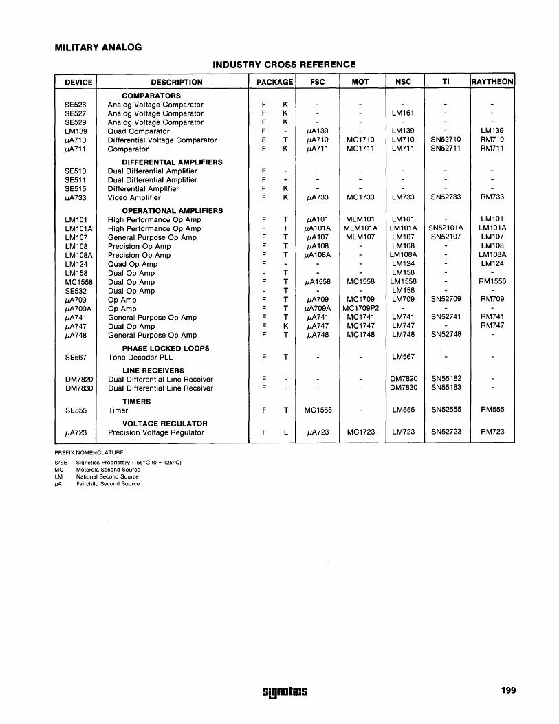
MILITARY ANALOG
INDUSTRY CROSS REFERENCE
DEVICE DESCRIPTION PACKAGE FSC MOT NSC TI RAYTHEON
COMPARATORS SE526 Analog Voltage Comparator F K - - - - -SE527 Analog Voltage Comparator F K - - LM161 - -SE529 Analog Voltage Comparator F K - - - - -LM139 Quad Comparator F - fJ.A139 - LM139 - LM139
fJ.A710 Differential Voltage Comparator F T fJ.A710 MC1710 LM710 SN52710 RM710 fJ.A711 Comparator F K fJ.A711 MC1711 LM711 SN52711 RM711
DIFFERENTIAL AMPLIFIERS SE510 Dual Differential Amplifier F - - - - - -SE511 Dual Differential Amplifier F - - - - - -SE515 Differential Amplifier F K - - - - -fJ.A733 Video Amplifier F K fJ.A733 MC1733 LM733 SN52733 RM733
OPERATIONAL AMPLIFIERS LM101 High Performance Op Amp F T fJ.A 101 MLM101 LM101 - LM101
LM101A High Performance Op Amp F T fJ.A1 01 A MLM101A LM101A SN52101A LM101A LM107 General Purpose Op Amp F T fJ.A107 MLM107 LM107 SN52107 LM107 LM108 Precision Op Amp F T fJ.A 108 - LM108 - LM108 LM108A Precision Op Amp F T fJ.A108A - LM108A - LM108A LM124 Quad Op Amp F - - - LM124 - LM124 LM158 Dual Op Amp - T - - LM158 - -MC1558 Dual Op Amp F T fJ.A1558 MC1558 LM1558 - RM1558 SE532 Dual Op Amp - T - - LM158 - -fJ.A709 OpAmp F T fJ.A709 MC1709 LM709 SN52709 RM709 fJ.A709A OpAmp F T fJ.A709A MC1709P2 - - -fJ.A741 General Purpose Op Amp F T fJ.A741 MC1741 LM741 SN52741 . RM741
fJ.A747 Dual Op Amp F K fJ.A747 MC1747 LM747 - RM747
fJ.A748 General Purpose Op Amp F T fJ.A748 MC1748 LM748 SN52748 -
PHASE LOCKED LOOPS SE567 Tone Decoder PLL F T - - LM567 - -
LINE RECEIVERS DM7820 Dual Differential Line Receiver F - - - DM7820 SN55182 -DM7830 Dual Differential Line Receiver F - - - DM7830 SN55183 -
TIMERS SE555 Timer F T MC1555 - LM555 SN52555 RM555
VOLTAGE REGULATOR fJ.A723 Precision Voltage Regulator F L fJ.A723 MC1723 LM723 SN52723 RM723
PREFIX NOMENCLATURE
S/SE Signetics Proprietary (-55°C to + 125°C) MC Motorola Second Source LM National Second Source !-IA Fairchild Second Source
!ii!)notiC!i 199

How can you switch to bipolar from MOS microprocessing without obsoleting your existing designs? How can you reduce hardware design time, reduce programming time, reduce debugging time? How can you try it before you buy it?
Signetics has put it all together in bipolar microprocessors featuring the industry's most complete product family, fastest 2-bit j.LPA (3001), first 8-bit fixed instruction processor (8X300), the 8080 emulator, several designers' kits, interface elements, bipolar memories and all using Signetics superior low power Schottky LSI technology.
• 8080 Emulator upgrades performance of existing system. Delivers 5 times more performance, reduces micro-code writing time, operates from existing software, makes designing easy. (Available now.)
• A free microprocessing book. It's filled with memory, logic, interface info and application notes. All
Signetics' high performance bipolar products are listed in detail.
• The industrY's leading selection of RAM's, ROM's, PROM's, FPLA's, you name it. Signetics has more configurations and performance levels available from stock. You get the right fit and absolute maximum efficiency in minimum time.
• 8X3OO Designer's Kit. We supply all the parts you need to build your own general purpose controlleryou do the PROM programming, checkout prototype system, order production quantities from Signetics. It's just another example of Signetics total support.
• Long list of interface products to pick from. Signetics has the interface products you'll need to make your bipolar microprocessing shopping easier and more convenient. Now you get everything on your list from one source.
@) Introductory Designer's Kit. A $230.00 value, for $100.00. You get 12 parts and 1 manual to let you work with bipolar, design with bipolar, program

with bipolar, and prove out all the advantages for yourself. The parts you need to actually try out Signetics' 3000 Thtal System.
• A description of all design support systems. Read all about 'em. SMS ROM Simulator, SMS McSim Prototyping System, Microassembler, SMS McCAP Assembler and more, all in the microprocessor book.
Field Applications Engineers that know bipolar microprocessing. They have the industry's best support systems at hand to help you solve your design problems. They will show you exactly how Signetics' total bipolar microprocessor capabilities will make your design resources go further.
N ow you know when Signetics claims to reduce your hardware design time, to reduce your programming time, and to reduce your debugging time ... Signetics supports it. Start saving time in the future by mailing the coupon today.
r---~~~~;~;~~~~:~;~;~;:;-~--
o Send me information on the 3000 Introductory Designer's Kit .
D Send me information on the 8X300 Designer's Kit-to dream up my own controllers.
o I want to read the book on bipolar microprocessing. Send it ASAP. FREE.
D Send me info now on an emulator that delivers 5 times more performance, the 8080.
o Have a Bipolar Microprocessing Answerman call me for an appointment.
My application is ______________ _
Name Title
l(gnDliCI a subsidiary of Us. PIiIips Corporation
Signetics Corporation 811 East Arques Averoo
Sunnyvale, California 94086 Telephone 408/739-7700
SIGNETICS onawa. Ontario
HEADQUARTERS Philips Electronics Industries Ltd.
Phone: (613) 237-3131 811 East Arques Avenue Scarborough. Ontario Sunnyvale. California 94086 Philips Electronics, Phone: (408) 739-7700 Industries Ltd. ARIZONA Phone: (416) 292-5161
Phoenix Vancouver. B.C. Phone: (602) 971-2517 Philips Electronics
Industries Ltd. CALIFORNIA Phone: (604) 435-4411 Inglewood COLORADO Phone: (213) 670-1101
Denver Irvine Barnhill Five. Inc. Phone: (714) 833-8980 Phone: (303) 426-0222 (21-3) 924-1668 CONNECTICUT San Diego Newtown Phone: (714) 560-0242 Kanan Associates
Sunnyvale Phone: (203) 426-8157 Phone: (408) 736-7565 COLORADO FLORIDA
Altamonte Springs Parker Phone: (303) 841-3274
Semtronic Associates Phone: (305) 831-8233
flORIDA Pompano Beach
Largo Semtronic Associates
Phone: (305) 782-8225 Phone: (813) 586-1404 ILLINOIS IlliNOIS Rolling Meadows Chicago Phone: (312) 259-8300 l-Tec Inc. INDIANA Phone: (312) 286-1500 Noblesville KANSAS Phone: (317) 773-6770 Lenexa KANSAS Buckman & Associates Wichita Phone: (913) 492-8470 Phone: (316) 683-6035 MARYLAND
MASSACHUSETTS Glen Burni
Woburn Microcomp. Inc.
Phone: (617) 933-8450 Phone: (301) 761-4600
MICHIGAN MASSACHUSETTS
Southlield Reading Phone: (313) 645-1232 Kanan Associates
MINNESOTA Phone: (617) 944-8484 MICHIGAN
Edina Phone: (612) 835-7455 Bloomlield Hills
Enco Marketing NEW JERSEY Phone: (313) 642-0203 Cherry Hill MINNESOTA Phone: (609) 665-5071
Edina Piscataway Mel Foster Tech. Assoc. Phone: (201) 981-0123 Phone: (612) 835-2254 NEW YORK MISSOURI Wappingers Falls St. Charles Phone: (914) 297-4074 Buckman & Associates Woodbury.l.I. Phone: (314) 724-6690 Phone: (516) 364-9100 NEW JERSEY OHIO Haddonfield Worthington Thomas Assoc .. Inc. Phone: (614) 888-7143 Phone: (609) 854-3011 TEXAS NEW MEXICO Dallas Albuquerque Phone: (214) 661-1296 The Staley Company. Inc.
Phone: (505) 821-4310/11 NEW YORK
REPRESENTATIVES Ithaca Bob Dean. Inc. Phone: (607) 272-2187
ARIZONA NORTH CAROLINA Phoenix
Chaparral-Dorton Cary Phone: (602) 263-0414 Montgomery Marketing
CALIFORNIA Phone: (919) 467-6319 OHIO
San Diego Mesa Engineering Centerville Phone (714) 278-8021 Norm Case Associates
Sherman Oaks Phone: (513) 433-0966
Astralonics Fairview Park Phone: (213) 990-5903 Norm Case Associates
CANADA Phone: (216) 333-4120
Calgary. Alberta OREGON
Philips Electronics Portland Industires ltd Western Technical Sales
Phone: (403) 243-7737 Phone: (503) 297-1711
Montreal. Quebec TEXAS Philips Electronics Dallas
Industries ltd. Cunningham Company Phone: (514) 342-9180 Phone: (214) 233-4303
Houston CONNECTICUT Cunningham Company Danbury Phone: (713) 461-4197 Schweber Electronics UTAH Phone: (203) 792-3500 West Bountiful Georgetown Barnhill Five. Inc. Hamiltonl Avnet Electronics Phone: (801) 292-8991 Phone: (203) 762-0361 WASHINGTON Hamden Bellevue Arrow Electronics Western Technical Sales Phone: (203) 248-3801 Phone: (206) 641-3900 flORIDA WISCONSIN Ft. Lauderdale Greenlield Arrow Electronics l-Tec. Inc. Phone: (305) 776-7790 Phone: (414) 545-8900 Hamiitonl Avnet Electronics
Phone: (305) 971-2900
DISTRIBUTORS Hollywood Schweber Electronics
ALABAMA Phone: (305) 922-4506
Huntsville Orlando Hamiltonl Avnet Electronics Hammond Electronics
Phone: (305) 241-6601 Phone (205) 533-1170 ARIZONA GEORGIA
Phoenix Allanla Hamiltonl Avnet Electronics Schweber Electronics Phone: (602) 275-7851 Phone: (404) 449-9170
Norcross liberty Electronics Hamiitonl Avnet Electronics Phone: (602) 257-1272 Phone: (404) 448-0800
CAUFORNIA ILLINOIS Costa Mesa
Schweber Electronics Elk Grove Schweber Electronics Phone: (714) 556-3880 Phone: (312) 593-2740 Culver City Elmhurst Hamilton Electro Sales
Phone: (213) 558-2173 Semiconductor Specialists
EI Segundo Phone: (312) 279-1000
liberty Electronics Schieler Park Phone: (213) 322-8100 Hamiltonl Avnet Electronics
Mountain View Phone: (312) 671-6082
Elmar Electronics INDIANA Phone: (415) 961-3611 Indianapolis Hamilton! AIInet Electronics Semiconductor Specialists Phone: (415) 961-7000 Phone: (317) 243-8271
San Diego KANSAS Hamiltonl Avnet Electronics Lenexa Phone: (714) 279-2421 Hamiltonl Avnet Electronics liberty Electronics Phone: (913) 888-8900 Phone: (714) 565-9171 MARYLAND Sunnyvale Baltimore Intermark Electronics Arrow Electronics Phone: (408) 738-1111 Phone: (301) 247-5200 CANADA Gaithersburg Downsview. Ontario Pioneer Washington Cesco Electronics Electronics Phone: (416) 661-0220 Phone: (301) 948-0710
Mississauga. Ontario Hanover Hamiltonl Avnet Electronics Hamiltonl Avnet Electronics Phone: (416) 677-7432 Phone: (301) 796-5000
Montreal. Quebec Rockville Schweber Electronics Cesco Electronics Phone: (301) 881-2970 Phone: (514) 735-5511
Zentronics ltd. MASSACHUSETTS Phone: (514) 735-5361 Waltham
Schweber Electronics Onawa. Ontario Phone: (617) 890-8484 Hamiltonl Avnet Electronics
Phone: (613) 226-1700 Woburn Arrow Electronics Zentronics ltd. Phone: (617) 933-8130 Phone: (613) 238-6411
Toronto. Ontario Hamiltonl Avnet Electronics Zentronics ltd. Phone: (617) 933-8000 Phone: (416) 789-5111 MICHIGAN Vancouver. B.C. Farmington Bowtek Electronics Co .. ltd. Semiconductor Specialists Phone: (604) 736-1141 Phone: (313) 478-2700
Ville SI. Laurent. Quebec Livonia Hamiltonl Avnet ElectroniCS Hamiltonl Avnet Electronics Phone: (514) 331-6443 Phone: (313) 522-4700 COLORADO Troy Commerce City Schweber Electronics Elmar Electronics Phone: (313) 583-9242 Phone: (303) 287-9611 MINNESOTA Denver Eden Prairie Hamiltonl Avnet Electronics Schweber Electronics Phone: (303) 534-1212 Phone: (612) 941-5280 Lakewood Edina Acacia Sales. Inc. Hamiltonl Avnet Electronics Phone: (303) 232-2882 Phone: (612) 941-3801
Minneapolis Hamiltonl Avnet Electronics INDONESIA Semiconductor Specialists Phone: (214) 661-8204 P.T. Phlllps-Ralin Electronics Phone: (612) 854-8841 Schweber Electronics Jakarta MISSOURI Phone: (214) 661-5010 Phone: 581058 Hazelwood Houston IRAN Hamiltonl Avnet Electronics Component Specialists Berkeh Company. lid. Phone: (314) 731-1144 Phone: (713) 771-7237 Tehran NEW MEXICO Hamiltonl Avnet Electronics Phone: 831564 Albuquerque Phone: (713) 780-1771 ISRAEL Hamiltonl Avnet Electronics Schweber Electronics Rlpac Eleclronlcs. Ltd. Phone: (505) 765-1500 Pone: (713) 784-3600 Tel Aviv NEW YORK UTAH Phone: 477115-6-7 Buffalo Salt Lake City ITALY Summit Distributors Alta Electronics Philips S.p.A. Phone: (716) 884-3450 Phone: (801) 486-7227 Milano East Syracuse Hamiltonl Avnet Electronics Phone: 2-6994 Hamiltonl Avnet Electronics Phone: (801) 262-8451 JAPAN Phone: (315) 437-2642 WASHINGTON Signelics Japan. lid. Farmingdale. 1.I. Bellevue Tokyo Arrow Electronics Hamiltonl Avnet Electronics Phone: (03) 230-1521 Phone: (516) 694-6800 Phone: (206) 746-8750 KOREA Johnson City Seanle Wilshire Electronics Intermark Electronics
Philips Electronics Korea. Ltd. Seoul Phone: (607) 797-1236 Phone: (206) 767-3160 Phone: 44-4202
Rochester liberty Electronics MEXICO Hamiltonl Avnet Electronics Phone: (206) 763-8200 Phone: (716) 442-7820 Electronlca S.A. de C. V.
Schweber Electronics Mexico D.F.
Phone: (716) 461-4000 Phone: 533-1180
Westbury.l.I. NETHERLANOS
FOR SIGNETICS PRODUCTS Hamiltonl Avnet Electronics Philips Nederland B.V. Phone: (516) 333-5800 WORLDWIDE Eindhoven Schweber Electronics Phone: (040) 79 33 33 Pmne: (516) 334-7474 NEW ZEALAND
NORTHERN NEW JERSEY ARGENTINA E.D.A.C. Ltd.
Cedar Grove Fapesa I. y .C. Wellington
Hamilton/Avnet Electronics Buenos-Aires Phone: 873-159
Phone: (201) 239-0800 Phone: 652-743817478 NORWAY
Saddlebrook AUSTRIA Electronica A.S. Arrow Electronics Osterreichische Philips Oslo Phone: (201) 797-5800 Wien Phone: (02) 15 05 90
SOUTHERN NEW JERSEY Phone: 93 26 11 PHILIPPINES
AND PENNSYLVANIA AUSTRALIA Philips Industrial Dev .. Inc.
Cherry Hill. N.J. Philips Industries-ELCOMA Makata-Rizal Phone: 868951-9
Milgray-Delaware Valley lane-Cove N.SW. Phone: (609) 424-1300 Phone: 421261 SINGAPORE/MALAYSIA
BELGIUM Philips Singapore Pte .. Ltd. Moorestown. N.J. Arrowl Angus Electronics M.B.l.E. Toa Payoh Phone: (609) 235-1900 Bruselles Phone: 538811
Mt. Laurel. N.J. Phone: 523 00 00 SOUTH AFRICA Hamiltonl Avnet ElectroniCS BRAZIL E.D.A.C. IPTY). LId. Phone: (609) 234-2133 Ibrape. S.A. Johannesburg
CENTRAL NEW JERSEY Sao Paulo Phone: 24-6701-3
AND PENNSYLVANIA Phone: 287-7144 SPAIN
CANADA Copresa S.A. Someresl. N.J. Schweber Electronics Philips Electron Devices Barcelon"
Phone: (201) 469-6008 Toronto Phone: 329 63 12
Phone: 425-5161 SWEDEN Horsham. PA Schweber Electronics CHILE Elcoma A.B. Phone: (215) 441-0600 Philips Chilena S.A. Stockholm
Phone: 08/67 97 80 NORTH CAROLINA Phone: 39-4001 Greensboro DENMARK SWITZERLAND
Hammond Electronics Philips A.G. MiniwaU A/S Phone: (919) 275-6391 Kobenhavn Zurich
OHIO Phone: (01) 69 1622 Phone: 01144 22 11 TAIWAN Beechwood FINLAND
Schweber Electronics Philips Taiwan. lid. Phone: (216) 464-2970
Oy Philips Ab Taipei Helsinki Phone: (02) 551-3101-5 Cleveland Phone: 1 72 71 Arrow Electronics FRANCE THAILAND/LAOS Phone: (216) 464-2000 R.T.C. Sleng Thong Radio. lid.
Bangkok Hamiltonl Avnet Electronics Paris Phone: 527195. 519763 Phone: (216) 461-1400 Phone: 355-44-99 Pioneer Standard Electronics GERMANY UNITED KINGDOM Phone: (216) 587-3600 Valvo MUllard.lId. Dayton Hamburg London Arrow Electronics Phone: (040) 3296-1 Phone: 01-580 6633 Phone: (513) 253-9176 HONG KONG UNITED STATES Hamiltonl Avnet Electronics Philips Hong Kong. lid. Signatici International Corp. Phone: (513) 433-0610 Kwuntong Sunnyvale. California Pioneer Standard Electronics Phone: 3-427232 Phone: (408) 739-7700 Phone: (513) 236-9900 INDIA VENEZUELA. PANAMA. TEXAS Semiconductors. Ltd. ARUBA. TRINIDAD DaUas (REPRESENTATIVE ONLY) Inltrul.b C.A. Component Specialists Bombay Caracas Phone: (214) 357-6511 Phone: 293-667 Phone 614138
Feb. 1977