Embed Size (px)
Citation preview
University of Central Florida University of Central Florida
STARS STARS
Electronic Theses and Dissertations, 2004-2019
2012
Bst-inspired Smart Flexible Electronics Bst-inspired Smart Flexible Electronics
Ya Shen University of Central Florida
Part of the Electrical and Electronics Commons
Find similar works at: https://stars.library.ucf.edu/etd
University of Central Florida Libraries http://library.ucf.edu
This Doctoral Dissertation (Open Access) is brought to you for free and open access by STARS. It has been accepted
for inclusion in Electronic Theses and Dissertations, 2004-2019 by an authorized administrator of STARS. For more
information, please contact [email protected].
STARS Citation STARS Citation Shen, Ya, "Bst-inspired Smart Flexible Electronics" (2012). Electronic Theses and Dissertations, 2004-2019. 2483. https://stars.library.ucf.edu/etd/2483
BST-INSPIRED SMART FLEXIBLE ELECTRONICS
by
YA SHEN M.S. University of Central Florida, 2009
A dissertation submitted in partial fulfillment of the requirements for the degree of Doctor of Philosophy
in the Department of Electrical Engineering and Computer Science in the College of Engineering and Computer Science
at the University of Central Florida Orlando, Florida
Summer Term 2012
Major Professors: Xun Gong and Parveen Wahid

ii
© 2012 Ya Shen
iii
ABSTRACT
The advances in modern communication systems have brought about devices with more
functionality, better performance, smaller size, lighter weight and lower cost. Meanwhile, the
requirement for newer devices has become more demanding than ever. Tunability and
flexibility are both long-desired features. Tunable devices are ‘smart’ in the sense that they can
adapt to the dynamic environment or varying user demand as well as correct the minor
deviations due to manufacturing fluctuations, therefore making it possible to reduce system
complexity and overall cost. It is also desired that electronics be flexible to provide
conformability and portability.
Previously, tunable devices on flexible substrates have been realized mainly by dicing
and assembling. This approach is straightforward and easy to carry out. However, it will become
a “mission impossible” when it comes to assembling a large amount of rigid devices on a
flexible substrate. Moreover, the operating frequency is often limited by the parasitic effect of
the interconnection between the diced device and the rest of the circuit on the flexible
substrate. A recent effort utilized a strain-sharing Si/SiGe/Si nanomembrane to transfer a
device onto a flexible substrate. This approach works very well for silicon based devices with
small dimensions, such as transistors and varactor diodes. Large-scale fabrication capability is
still under investigation.
A new transfer technique is proposed and studied in this research. Tunable BST (Barium
Strontium Titanate) IDCs (inter-digital capacitors) are first fabricated on a silicon substrate. The
devices are then transferred onto a flexible LCP (liquid crystalline polymer) substrate using
iv
wafer bonding of the silicon substrate to the LCP substrate, followed by silicon etching. This
approach allows for monolithic fabrication so that the transferred devices can operate in
millimeter wave frequency. The tunability, capacitance, Q factor and equivalent circuit are
studied. The simulated and measured performances are compared. BST capacitors on LCP
substrates are also compared with those on sapphire substrates to prove that this transfer
process does not impair the performance.
A primary study of a reflectarray antenna unit cell is also conducted for loss and phase
swing performance. The BST thin film layout and bias line positions are studied in order to
reduce the total loss. Transferring a full-size BST-based reflectarray antenna onto an LCP
substrate is the ultimate goal, and this work is ongoing at the University of Central Florida
(UCF).
HFSS is used to simulate the devices and to prove the concept. All of the devices are
fabricated in the clean room at UCF. Probe station measurements and waveguide
measurements are performed on the capacitors and reflectarray antenna unit cells
respectively.
This work is the first comprehensive demonstration of this novel transfer technique.

v
Dedicated to my parents.

vi
ACKNOWLEDGMENTS
I am deeply in debt to the people who have been with me during these years of my Ph.D
study, people who have encouraged me in various ways at different times, and people who
have shared my joys and tears. I simply cannot imagine myself facing life’s challenges by myself.
Special thanks to my advisors and mentors, Dr. Wahid and Dr. Gong, for their
continuous teaching and support all these years. Even during my days of self-doubt and
uncertainty, they never gave up on me. I could not ask for more from any mentor.
Huge thanks to all the professors in my committee for their hard work and constructive
advice for my research and my dissertation. I feel very sorry for having you all go through my
first draft of the dissertation, which, when I look at it now, was kind of like a punishment.
Big thanks to all of my course professors who invested in me. I learned so much from all
of you that will surely benefit me for the rest of my life.
Many thanks to all my coworkers who have been working with me for years, some more
than the number of fingers on my hand. How can I forget those days when you guys generously
offered your time to help me proofread my papers, to prepare me for various presentation
occasions and even just to “chit-chat” to lower my stress?
A lot of thanks also go to all my friends from school, from my church family and
everywhere else. There are just too many of you so I’m not going to spend pages to list all the
names. Thanks for always being there for me whenever I needed you. It is such a blessing to
have you all in my life!

vii
And of course, most importantly, I would like to thank my parents. You are the ones
who have been there for me ever since I took my first breath. You are the ones who would still
love me whether I succeed or fail. I would not have accomplished so much in my life without
your teaching, encouragement and love. Hope this one more achievement will add in your
collection of “things I’m proud of for my girl”!
viii
TABLE OF CONTENTS
LIST OF FIGURES .............................................................................................................................. xi
LIST OF TABLES ............................................................................................................................. xvii
LIST OF ACRONYMS/ABBREVIATIONS ......................................................................................... xviii
CHAPTER ONE: INTRODUCTION ..................................................................................................... 1
1.1 Frequency-agile Technologies ....................................................................................................... 1
1.1.1 Semiconductors .................................................................................................................... 2
1.1.2 MEMS .................................................................................................................................... 4
1.1.3 Ferroelectric Materials .......................................................................................................... 8
1.1.4 A Comparison of the Current Available Tunable Technologies .......................................... 12
1.2 Flexible Electronics ...................................................................................................................... 13
1.2.1 Materials and Fabrication Techniques for Flexible Electronics .......................................... 15
1.2.2 LCP State-of-the-art Applications........................................................................................ 16
1.3 Tunable and Flexible – The Newly-mingled Field ....................................................................... 19
1.4 Dissertation Outline .................................................................................................................... 21
CHAPTER TWO: BST – A SMART MATERIAL ................................................................................. 23
2.1 BST Material Properties .............................................................................................................. 23
2.1.1 Ferroelectric Phenomenology ............................................................................................. 23
2.1.2 Bulk vs. Thin Film BST .......................................................................................................... 25
2.1.3 BST Thin Film Electrical Properties ...................................................................................... 26
2.2 BST Deposition Techniques ......................................................................................................... 29
2.2.1 RF Magnetron Sputter Deposition ...................................................................................... 29
2.2.2 Pulsed Laser Deposition PLD ............................................................................................... 32
2.2.3 Sol-gel .................................................................................................................................. 33
2.2.4 Chemical Vapor Deposition CVD ......................................................................................... 33
2.3 BST Analytical Techniques........................................................................................................... 34
2.4 BST Transfer Technique .............................................................................................................. 37
CHAPTER THREE: BST CAPACITOR ON FLEXIBLE SUBSTRATE ...................................................... 40
3.1 Layout Design of BST capacitors ................................................................................................. 40
ix
3.2 BST Thin Film on a Silicon Substrate ........................................................................................... 43
3.2.1 Thermal Incompatibility between BST Thin Film and Silicon Substrate ............................. 44
3.2.2 Deposition and Annealing Parameters for BST Thin Film on a Silicon Substrate ............... 46
3.2.3 Material Characterization of the BST Thin Film on a Silicon Substrate .............................. 46
3.3 BST IDC on Flexible LCP Substrate – Simulation ......................................................................... 48
3.4 BST IDC on Flexible LCP Substrate – Fabrication and Transfer ................................................... 54
3.5 BST IDC on Flexible LCP Substrate – Measurement Setup .......................................................... 60
3.6 Measurement Results and Discussions ....................................................................................... 62
3.6.1 Measured Results of BST IDC on LCP Substrate .................................................................. 62
3.6.2 BST IDC on an LCP substrate – Comparison of Measured and Simulated Results .............. 67
3.6.3 BST IDC Comparison of Measured Results on an LCP and a Sapphire Substrates .............. 72
3.6.4 Extraction of BST Permittivity Values and Loss Tangent Values from measurement ......... 74
CHAPTER FOUR: BST-BASED REFLECTARRAY ANTENNA UNIT CELL ............................................ 78
4.1 Why Reflectarray Antenna? ........................................................................................................ 79
4.1.1 Advantages and Disadvantages of Parabolic Reflector and Phased Array ......................... 79
4.1.2 Reflectarray Antenna .......................................................................................................... 80
4.2 Available Technologies for the Tunable Microstrip Patch Reflectarray antenna ....................... 81
4.3 BST-thin-film-based Reflectarray Antenna Unit Cell Design ....................................................... 84
4.3.1 Patch Size Design ................................................................................................................ 84
4.3.2 Proof of Concept: Lumped Capacitor vs. BST-loaded Gap .................................................. 89
4.3.3 BST thin film Layout Design................................................................................................. 92
4.3.4 Bias Line Layout Design ....................................................................................................... 93
4.4 X-band Reflectarray Antenna Unit Cell Simulation ..................................................................... 97
4.5 X-band Reflectarray Antenna Unit Cell Fabrication .................................................................. 100
4.6 X-band Reflectarray Antenna Unit Cell Measurement Setup ................................................... 104
4.7 Results and Discussions ............................................................................................................ 105
4.8 A Further Study of Bias Lines .......................................................................................................... 109
4.8.1 Optimum Bias Line Position .............................................................................................. 110
4.8.2 X-band Unit Cell Simulation .............................................................................................. 111
4.9 A Possible Upgrade – Ka-band Unit Cell Simulation ................................................................. 113
x
CHAPTER FIVE: CONCLUSION AND FUTURE WORK ................................................................... 117
APPENDIX A: SILICON ETCHING RATE BY KOH SOLUTION ......................................................... 119
APPENDIX B: CONVERSION OF S-PARAMETERS TO Y-PARAMETERS ......................................... 121
APPENDIX C: BST IDC ON LCP SUBSTRATE FABRICATION .......................................................... 123
APPENDIX D: BST-BASED REFLECTARRAY ANTENNA UNIT CELL FABRICATION ......................... 126
LIST OF REFERENCES ................................................................................................................... 129
xi
LIST OF FIGURES
Figure 1 - 1 Varactor Diode ............................................................................................................. 2
Figure 1 - 2 RF MEMS switch and capacitor .................................................................................... 4
Figure 1 - 3 Electrical field dependent permittivity ........................................................................ 8
Figure 2 - 1 BST molecule structure .............................................................................................. 24
Figure 2 - 2 polarization of BST material (a) Ferroelectric and (b) paraelectric ........................... 25
Figure 2 - 3 An RF sputtering system, (a) diagram, (b) targets, and (c) the inside picture of a 3-
gun sputtering system ............................................................................................. 31
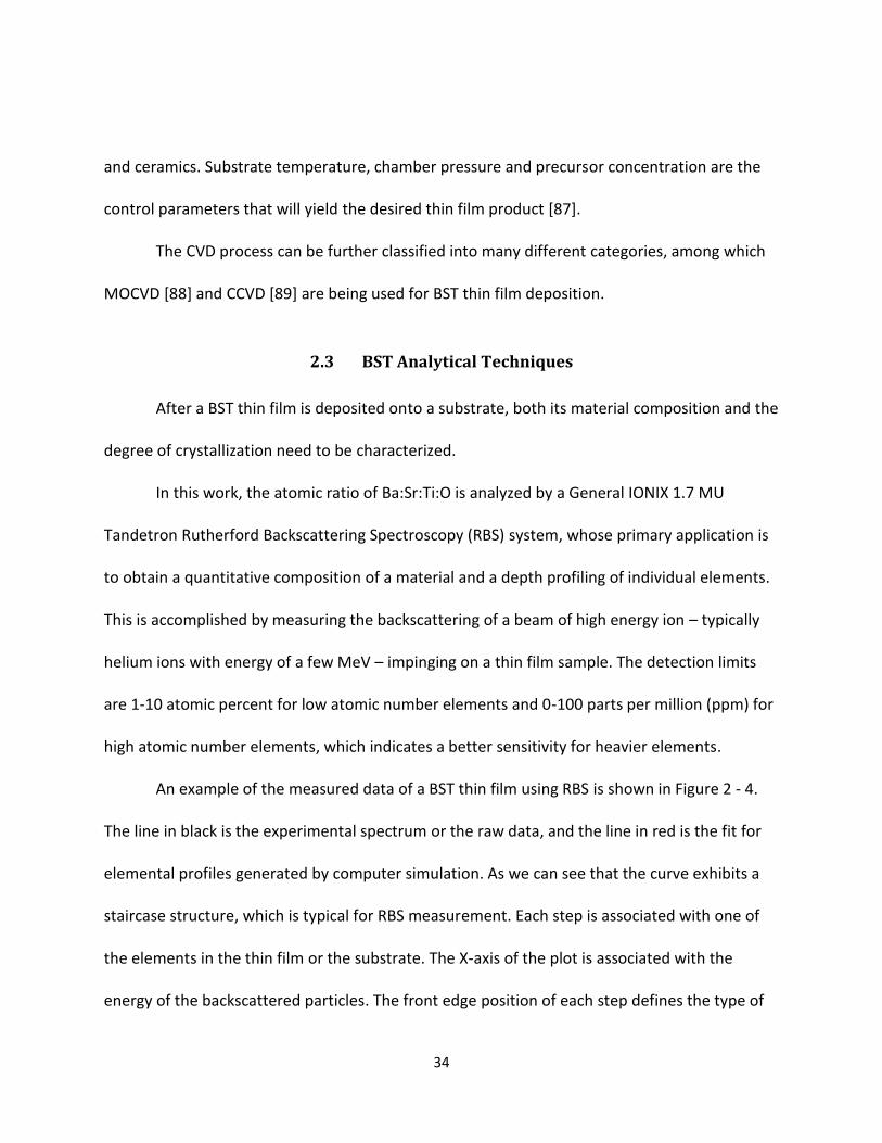
Figure 2 - 4 Sample data of an RBS measurement ....................................................................... 36
Figure 2 - 5 Sample data of an XRD measurement ....................................................................... 37
Figure 2 - 6 BST transfer technique .............................................................................................. 38
Figure 3 - 1 Capacitor with MIM structure ................................................................................... 41
Figure 3 - 2 Capacitor with IDC structure...................................................................................... 42
Figure 3 - 3 Different BST thin film cracking observed under the microscope with the same
magnification ........................................................................................................... 45
Figure 3 - 4 RBS result of a BST thin film on a silicon substrate ................................................... 47
Figure 3 - 5 XRD result of a BST thin film on a silicon substrate ................................................... 48
Figure 3 - 6 HFSS simulation for BST IDC on LCP substrate .......................................................... 49
Figure 3 - 7 Simulated variation of S11 with the BST permittivity εr ............................................ 50
Figure 3 - 8 BST IDC lumped element equivalent circuit .............................................................. 51
Figure 3 - 9 Extracted series capacitance Cs from HFSS simulation ............................................. 52
xii
Figure 3 - 10 Extracted series resistance Rs from HFSS simulation .............................................. 52
Figure 3 - 11 Extracted parasitic capacitance Cp from HFSS simulation ...................................... 52
Figure 3 - 12 Extracted parasitic conductance Gp from HFSS simulation .................................... 53
Figure 3 - 13 Extracted Q factor from HFSS simulation ................................................................ 53
Figure 3 - 14 PR overhanging or under-cutting effect .................................................................. 57
Figure 3 - 15 A fixture used in silicon etching process to protect the LCP substrate from being
etched by silicon etchant ........................................................................................ 58
Figure 3 - 16 Fabrication process for the BST IDC on LCP substrate ............................................ 59
Figure 3 - 17 BST IDC on an LCP substrate (a) bent (b) under the microscope ............................ 60
Figure 3 - 18 Agilent 110 GHz N5250A PNA and Cascade Microtech M150 probe station .......... 61
Figure 3 - 19 Picosecond Pulse Labs model 5543 bias tee............................................................ 61
Figure 3 - 20 BST IDC being measured using Cascade Microtech GSG 150 probes ...................... 62
Figure 3 - 21 S11 with DC bias voltage variation for the BST IDC on LCP substrate ..................... 63
Figure 3 - 22 Extracted series capacitance Cs with DC bias voltage variation for the BST IDC on
LCP substrate ........................................................................................................... 63
Figure 3 - 23 Extracted series resistance Rs with DC bias voltage variation for the BST IDC on LCP
substrate .................................................................................................................. 64
Figure 3 - 24 Extracted parasitic capacitance Cp with DC bias voltage variation for the BST IDC
on LCP substrate ...................................................................................................... 64
Figure 3 - 25 Extracted parasitic Conductance Gp with DC bias voltage variation for the BST IDC
on LCP substrate ...................................................................................................... 64
xiii
Figure 3 - 26 Extracted Q factor with DC bias voltage variation for the BST IDC on LCP substrate
................................................................................................................................. 65
Figure 3 - 27 Extracted tunability for the BST IDC on LCP substrate ............................................ 67
Figure 3 - 28 Measured S11 vs. simulated S11 ............................................................................. 68
Figure 3 - 29 Measured Cs vs. simulated Cs .................................................................................. 68
Figure 3 - 30 Measured Rs vs. simulated Rs ................................................................................. 69
Figure 3 - 31 Measured Cp vs. simulated Cp ................................................................................ 70
Figure 3 - 32 Measured Gp vs. simulated Gp ................................................................................ 70
Figure 3 - 33 Measured Q factor vs. simulated Q factor .............................................................. 71
Figure 3 - 34 S11 measured on an LCP substrate vs. on a sapphire substrate ............................. 72
Figure 3 - 35 Cs measured on an LCP substrate vs. on a sapphire substrate ............................... 73
Figure 3 - 36 Rs measured on an LCP substrate vs. on a sapphire substrate ............................... 73
Figure 3 - 37 Cp measured on an LCP substrate vs. on a sapphire substrate ............................... 73
Figure 3 - 38 Gp measured on an LCP substrate vs. on a sapphire substrate .............................. 74
Figure 3 - 39 Q factor measured on an LCP substrate vs. on a sapphire substrate...................... 74
Figure 3 - 40 Extracted BST permittivity vs. frequency for different DC bias voltages ................ 75
Figure 3 - 41 Extracted BST loss tangent vs. frequency for different DC bias voltages ................ 75
Figure 3 - 42 Extracted BST permittivity and loss tangent vs. bias voltage at 10 GHz ................. 76
Figure 3 - 43 Extracted BST permittivity and loss tangent vs. bias voltage at 30 GHz ................. 76
Figure 3 - 44 Extracted BST permittivity and loss tangent vs. bias voltage at 50 GHz ................. 77
Figure 4 - 1 A 7 by 7 microstrip-patch-antenna-based reflectarray antenna ............................... 81
xiv
Figure 4 - 2 A reflectarray antenna with BST-based capacitive loading ....................................... 83
Figure 4 - 3 Reflectarray antenna unit cell with a square patch ................................................... 86
Figure 4 - 4 HFSS waveguide simulation of a reflectarray antenna unit cell with a square patch 87
Figure 4 - 5 HFSS simulation of a reflectarray antenna unit cell with a square patch (a) S11
magnitude, (b) S11 phase ........................................................................................ 88
Figure 4 - 6 Reflectarray antenna unit cell (a) lumped capacitor loading, (b) BST loading .......... 89
Figure 4 - 7 HFSS simulation results of a reflectarray antenna unit cell with lumped capacitor
loading. (a) S11 magnitude, (b) S11 phase, and (c) phase swing ............................ 90
Figure 4 - 8 HFSS simulation results of a reflectarray antenna unit cell with BST loading. (a) S11
magnitude, (b) S11 phase, and (c) phase swing ...................................................... 91
Figure 4 - 9 Different designs of BST thin film layout (a) BST thin film covering the entire
substrate, (b) BST thin film only under the gap area .............................................. 92
Figure 4 - 10 S11 magnitude comparison of reflectarray antenna unit cells with small BST thin
film and large BST thin film ..................................................................................... 93
Figure 4 - 11 Different bias line configurations for reflectarray antenna unit cell (a) no bias line,
(b) horizontal bias lines in the middle, (c) vertical bias lines in the middle, (d)
horizontal bias lines in the center, (e) vertical bias lines in the corner, (f) horizontal
bias lines in the corner ............................................................................................ 94
Figure 4 - 12 Current distribution for reflectarray antenna unit cell with different bias lines (a)
no bias line, (b) horizontal bias lines in the middle, (c) vertical bias lines in the
xv
middle, (d) horizontal bias lines in the center, (e) vertical bias lines in the corner,
(f) horizontal bias lines in the corner ...................................................................... 95
Figure 4 - 13 HFSS simulation of S11 for different bias line configurations (a) S11 magnitude of
unit cells with horizontal bias lines and without bias line, (b) S11 magnitude of unit
cells with vertical bias lines and without bias line, (c) S11 phase of unit cells with
horizontal bias lines and without bias line, (d) S11 phase of unit cells with vertical
bias lines and without bias line ............................................................................... 96
Figure 4 - 14 HFSS waveguide simulation of a reflectarray antenna unit cell with BST loading and
bias lines .................................................................................................................. 98
Figure 4 - 15 HFSS simulation results of a reflectarray antenna unit cell with BST loading. (a) S11
magnitude, (b) S11 phase, and (c) phase swing. ..................................................... 99
Figure 4 - 16 Reflectarray antenna unit cell fabrication procedure for the front side ............... 103
Figure 4 - 17 Reflectarray antenna unit cell illustration and microscopic pictures .................... 104
Figure 4 - 18 Reflectarray antenna unit cell measurement setup .............................................. 105
Figure 4 - 19 Reflectarray antenna unit cell measurement results (a) S11 magnitude, (b) S11
phase, and (c) phase swing ................................................................................... 106
Figure 4 - 20 Extracted BST permittivity and loss tangent.......................................................... 109
Figure 4 - 21 E-field shifts with lumped capacitance variation ................................................... 110
Figure 4 - 22 HFSS simulation results of a reflectarray antenna unit cell with BST loading and
optimized bias lines. (a) S11 magnitude, (b) S11 phase, and (c) phase swing ...... 112
Figure 4 - 23 HFSS waveguide simulation of a reflectarray antenna unit cell in Ka-band.......... 114

xvi
Figure 4 - 24 HFSS simulation results of a reflectarray antenna unit cell in Ka-band (a) S11
magnitude, (b) S11 phase, and (c) phase swing .................................................... 115
xvii
LIST OF TABLES
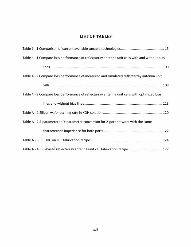
Table 1 - 1 Comparison of current available tunable technologies .............................................. 13
Table 4 - 1 Compare loss performance of reflectarray antenna unit cells with and without bias
lines ....................................................................................................................... 100
Table 4 - 2 Compare loss performance of measured and simulated reflectarray antenna unit
cells ........................................................................................................................ 108
Table 4 - 3 Compare loss performance of reflectarray antenna unit cells with optimized bias
lines and without bias lines ................................................................................... 113
Table A - 1 Silicon wafer etching rate in KOH solution ............................................................... 120
Table A - 2 S-parameter to Y-parameter conversion for 2-port network with the same
characteristic impedance for both ports............................................................... 122
Table A - 3 BST IDC on LCP fabrication recipe ............................................................................. 124
Table A - 4 BST-based reflectarray antenna unit cell fabrication recipe .................................... 127
xviii
LIST OF ACRONYMS/ABBREVIATIONS
BOX Buried Oxide
BOE Buffered Oxide Etch
BPF Band-Pass Filter
BST Barium Strontium Titanate
CCVD Combustion Chemical Vapor Deposition
CNT Carbon Nanotube
CPW Coplanar Waveguide
CVD Chemical Vapor Deposition
CTE Coefficient of Thermal Expansion
DI Water Deionized Water
DMTL Distributed Microelectromechanical Transmission Line
DRAM Dynamic Random Access Memories
EBG Electromagnetic-bandgap
EDP Ethylene Diamine Pyrocatechol
EM Electromagnetic
FOM Figure of Merit
FSS Frequency-selective surfaces
GaAs Gallium Arsenide
IDC Inter-Digital Capacitor
LCP Liquid Crystalline Polymer
xix
LNA Low Noise Amplifier
LPF Low-Pass Filter
MEMS Micro-Electro-Mechanical Systems
MIM Metal-Insulator-Metal
MMIC Monolithic Microwave Integrated Circuit
MMW Millimeter Wave
MOCVD Metalorganic Chemical Vapor Deposition
NEC Nantenna Electromagnetic Collector
NWT Nanowire Transistor
OLED Organic Light-emitting Diode
PA Power Amplifier
PCB Printed Circuit Board
PLD Pulsed Laser Deposition
PPM Parts-Per-Million
PR Photoresist
PVD Physical Vapor Deposition
PZT Lead Zirconate Titanate
RBS Rutherford Backscattering Spectroscopy
RF Radio Frequency
RFID Radio Frequency Identification
RPM Revolutions Per Mnute
xx
SBT Strontium Bismutate Tantalate
SCCM Standard Cubic Centimeter per Minute
SiNM Silicon-nanomembrane
SOP System-on-package
SSP Single Side Polish
TMAH Tetra Methyl Ammonium Hydroxide
TMN Tunable Matching Network
UHV Ultra High Vacuum
UWB Ultra-wideband
VCO Voltage Controlled Oscillator
XRD X-Ray Diffraction
1
CHAPTER ONE: INTRODUCTION
Advances in science and technology since the vacuum tube era have brought about the
rapid evolution in electronic devices. While the ever-increasing demands of enhanced
functionality, downscaled dimension and reduced cost have attracted the spotlight during the
20th century, tunability and flexibility are emerging needs for contemporary electronics. The
driving force behind this recent focus of interest is indisputable. Tunable devices are ‘smart’ in
the sense that they can adapt to the dynamic environment, varying user demands as well as
correct the minor deviations due to manufacturing fluctuations. This favorable feature makes it
possible to reduce system complexity and thus overall cost. On the other hand, flexible
electronics are desired for their many virtues, such as conformability, portability – being light
and able to be rolled up and deployed – and low-cost, thanks to the use of lightweight, flexible
and inexpensive substrates.
A lot of research effort and progress has been made in the area of tunable radio
frequency (RF) and microwave devices and in the field of flexible electronics respectively. Only
during recent years has the possibility of combining the two wonderful properties become
evident.
1.1 Frequency-agile Technologies
Tunable RF and microwave devices are often referred to as frequency-agile devices
because of their ability to quickly shift the operating frequency to accommodate different
2
needs. This category includes filters, phase shifters, matching networks, and voltage controlled
oscillators (VCO), to name a few. The frequency band for RF and microwave devices generally
covers anywhere from 20 kHz to 300 GHz. The three most frequently used technologies that are
available in the commercial market are semiconductors, micro-electro-mechanical systems
(MEMS) and ferroelectric materials [1] – [3].
1.1.1 Semiconductors
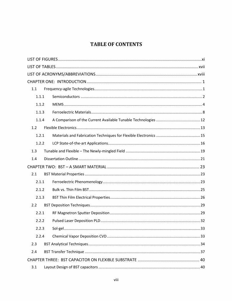
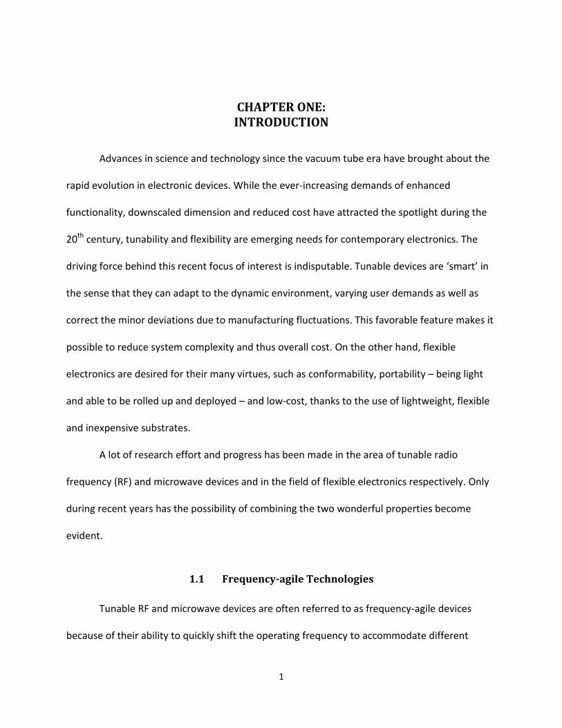
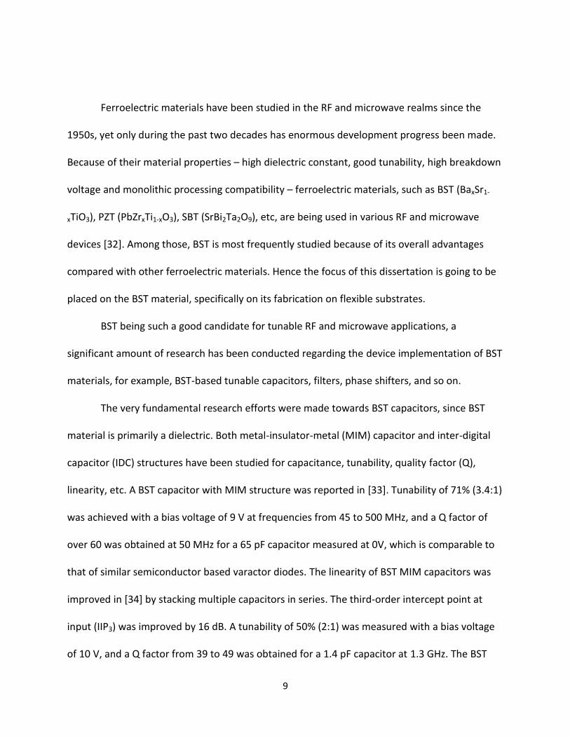
The semiconductor-based varactor diode is the earliest-matured technology among the
three technologies mentioned above in the electronics industry. It utilizes a reversely biased PN
junction to realize capacitance tuning, as shown in Figure 1 - 1 [4]. As the reverse bias voltage
increases, the width of the depletion region grows, thus the capacitance decreases, and vice
versa. This effect is equivalent to changing the distance between the plates of a metal-
insulator-metal capacitor in order to adjust its capacitance [5].
Figure 1 - 1 Varactor Diode
Because of its tuning mechanism, the varactor diode offers fast and continuous tuning,
yet it is inexpensive for mass production. However, it has disadvantages that limit its
3
applications, such as low quality factor at microwave frequencies, nonlinear C/V characteristics
and low power handling capacity.
Presently, varactor diodes are being used in two main areas: tunable filters and VCOs [6]
– [10]. Their main operating frequencies are within several GHz.
The tunable filters have always been a popular research topic. An early study of a
varactor-diode-based coplanar waveguide (CPW) slotline bandpass filter in the 1990’s showed a
tuning bandwidth of 600 MHz at the center frequency of 3 GHz (20% tuning) with a maximum
insertion loss of 2.15 dB. This tuning was achieved with a maximum bias voltage of 25 V [6]. A
later study of a varactor-diode-tuned filter using a suspended stripline showed a tuning range
from 0.7 to 1.33 GHz (60% tuning) with less than 3 dB of insertion loss. The maximum bias
voltage applied was 30 V [7]. More recent research results showed several resonator-based
two-pole filters using varactor diodes as tuning elements with a tuning range of 0.85 to 1.4 GHz
(50% tuning) with no more than 3.5 dB of insertion loss. A maximum bias voltage of 22 V was
used [8].
The VCOs have also been studied extensively. Research in the 1990’s showed a VCO
utilizing a varactor diode achieved a tuning of 9% at 4 GHz with a control voltage of 1 – 3 V. The
phase noise was measured at -106 dBc/Hz at 1 MHz and -85 dBc/Hz at 100 kHz [9]. A more
recent study of a varactor-diode-tuned VCO showed an improved phase noise of -110.5 – 108
dBc/Hz at 100 kHz that can be tuned from 5.4 to 5.8 GHz with a maximum bias voltage of 26 V
[10].
4
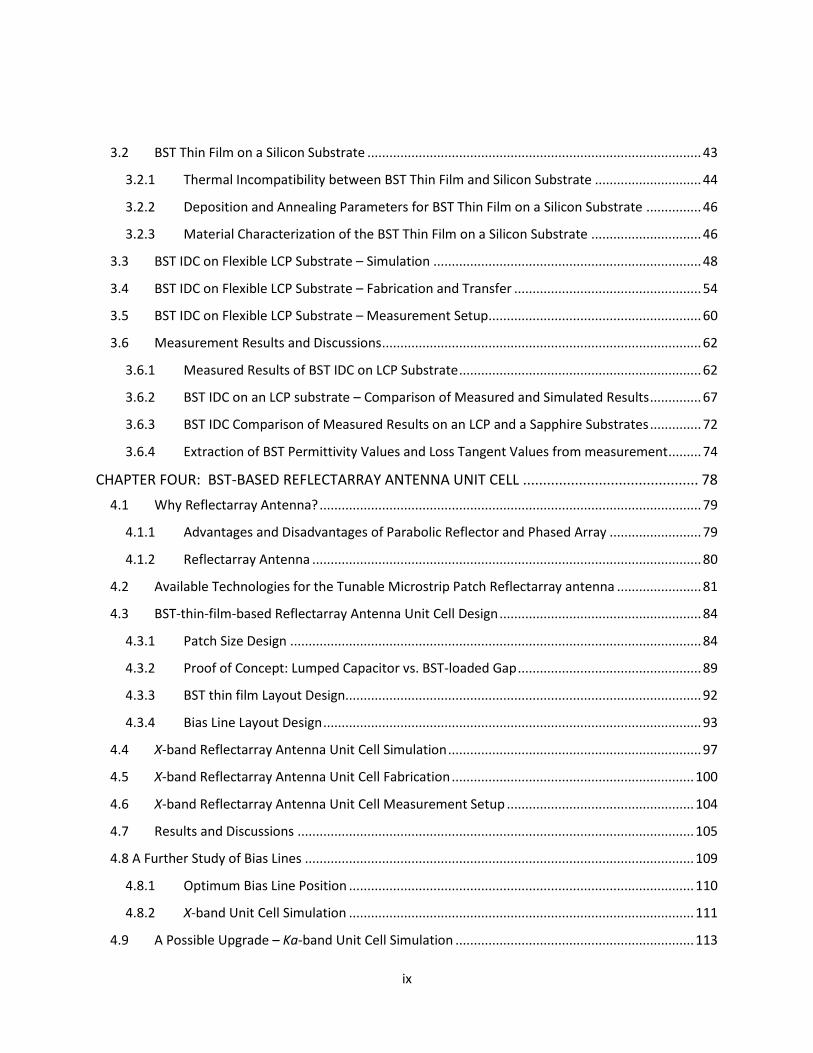
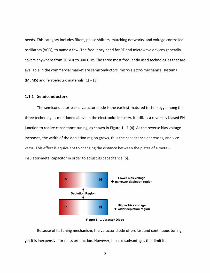
1.1.2 MEMS
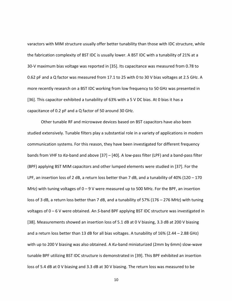
RF MEMS switches and capacitors belong to another popular category of frequency-
agile technology. MEMS – from its name, micro-electro-mechanical systems – traditionally refer
to miniature structures (usually sub-millimeter in dimension) that combine mechanical and
electrical functions. A demonstration of a basic MEMS switch and capacitor is shown in Figure 1
- 2 [1]. Upon applying an electrostatic force, the device changes its state from isolating position
(OFF) to conducting position (ON). Based on the type of dielectric material, this ON state can be
either conductive – a switch – or capacitive – a capacitor, as the demonstration in Figure 1 - 2
shows. This mechanism means that the tuning of the basic MEMS devices is typically discrete:
on and off [11] [12]. However, with some special designs, MEMS devices can be made to
perform continuous tuning.
Figure 1 - 2 RF MEMS switch and capacitor
Substrate
Substrate
Post Post
Post Post
MetalConducting or
dielectric material
OFF
Electrostatic Force
ON
5
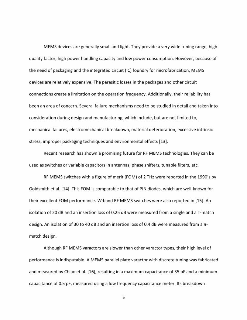
MEMS devices are generally small and light. They provide a very wide tuning range, high
quality factor, high power handling capacity and low power consumption. However, because of
the need of packaging and the integrated circuit (IC) foundry for microfabrication, MEMS
devices are relatively expensive. The parasitic losses in the packages and other circuit
connections create a limitation on the operation frequency. Additionally, their reliability has
been an area of concern. Several failure mechanisms need to be studied in detail and taken into
consideration during design and manufacturing, which include, but are not limited to,
mechanical failures, electromechanical breakdown, material deterioration, excessive intrinsic
stress, improper packaging techniques and environmental effects [13].
Recent research has shown a promising future for RF MEMS technologies. They can be
used as switches or variable capacitors in antennas, phase shifters, tunable filters, etc.
RF MEMS switches with a figure of merit (FOM) of 2 THz were reported in the 1990’s by
Goldsmith et al. [14]. This FOM is comparable to that of PIN diodes, which are well-known for
their excellent FOM performance. W-band RF MEMS switches were also reported in [15]. An
isolation of 20 dB and an insertion loss of 0.25 dB were measured from a single and a T-match
design. An isolation of 30 to 40 dB and an insertion loss of 0.4 dB were measured from a π-
match design.
Although RF MEMS varactors are slower than other varactor types, their high level of
performance is indisputable. A MEMS parallel plate varactor with discrete tuning was fabricated
and measured by Chiao et al. [16], resulting in a maximum capacitance of 35 pF and a minimum
capacitance of 0.5 pF, measured using a low frequency capacitance meter. Its breakdown
6
voltage, over 200 V, was much higher than that of a varactor diode. Another recent report of a
MEMS tunable capacitor with a continuous tuning range of 8.4:1 showed a high Q factor of
greater than 200 measured over the frequencies from 225 to 400 MHz [17]. Both of these
devices showed an exceptional tuning capacity which is superior to either the varactor diode or
the ferroelectric tunable capacitor.
RF MEMS switch or varactor based antennas require extra caution during design, since
antennas are generally very sensitive to surrounding structures and feeding variations. An early
effort of a tunable antenna integrating MEMS technology demonstrated a scanning angle of 48o
at 17.5 GHz. Directivity was estimated to be around 38 [18]. A V-band 2-D beam-steering
antenna applying MEMS technology was reported in [19]. This antenna was driven by magnetic
force and reached a maximum scanning angle of 40o.
An RF MEMS phase shifter design can employ many different topologies, such as
loaded-line phase shifters, reflection phase shifters, delay line phase shifters, etc. Although
MEMS phase shifters provide much lower loss than those based on monolithic microwave
integrated circuit (MMIC) technology, they suffer from slow tuning speed, normally in the order
of microseconds (µs). A 0 – 60 GHz wide band loaded line phase shifter has been developed in
[20], with a phase shift of 118o and an insertion loss of 2 dB when measured at 60 GHz. A phase
shift of 84o and insertion loss of 1.8 dB was measured at 40 GHz. The return loss was better
than 10 dB for both cases. Two other W-band loaded line phase shifters have also been
demonstrated in [21]. For the 3-bit distributed microelectromechanical transmission line
(DMTL) configuration, phase shifts of 45o, 90o, 135o, 180o, 225o, 270o and 315o were achieved,
7
and an average insertion loss of 2.7 dB and a return loss better than 10 dB were measured at 78
GHz. For the 2-bit DMTL configuration, phase shifts of 89o, 180o and 272o were achieved, and an
average insertion loss of 2.2 dB and return loss better than 11 dB was measured at 81 GHz. A
reflection phase shifter was reported in [22]. This 4-bit circuit provided a phase shift from 0 to
337.5o in 22.5o steps. An average insertion loss of 1.4 dB and a return loss better than 11 dB
were measured for all 16 states. Two delay line phase shifters, one with 3-bit and the other
with 4-bit, were reported in [23]. The 3-bit phase shifter had an average insertion loss of 1.7 dB
and a return loss better than 13 dB for all 16 states from 0o to 337.5o with 22.5o increments.
The 4-bit phase shifter had an average insertion loss of 2.25 dB and a return loss better than 15
dB for all 8 states from 0o to 315o with 45o increments.
RF MEMS tunable filters have been studied intensively for all frequency bands. A
differential 4-bit MEMS band-pass filter designed from 6.5 to 10 GHz was reported in [24]. A
44% tuning range was achieved with return loss better than 16 dB for the whole frequency
range. Insertion losses of 4.1 dB and 5.6 dB were measured at 9.8 and 6.5 GHz respectively.
Fractional bandwidths of 4.7% and 5.5% were obtained. A Ku-band RF MEMS tunable band-pass
filter was reported in [25]. A tunability of 44% (from 9.55 to 14.95 GHz), an insertion loss less
than 3.2 dB, a return loss better than 15 dB and a fractional bandwidth of 5.3-5.8% were
measured. A miniature three-pole slow-wave RF MEMS band pass filter at 18-22 GHz was
developed in [26]. This filter exhibited a tuning range of 14% (from 18.6 to 21.4 GHz), an
insertion loss of 3.85-4.15 dB and a fractional bandwidth of 7.5%.
8
In addition to RF and microwave applications, MEMS devices have made their way into
numerous fields in the last half a century, for instance, fluidics, thermodynamics, acoustics,
electromagnetics, chemistry, biology, optics, etc [27] – [29]. Therefore the name MEMS has also
outgrown its classical definition as many MEMS devices nowadays do not involve mechanical
movement anymore.
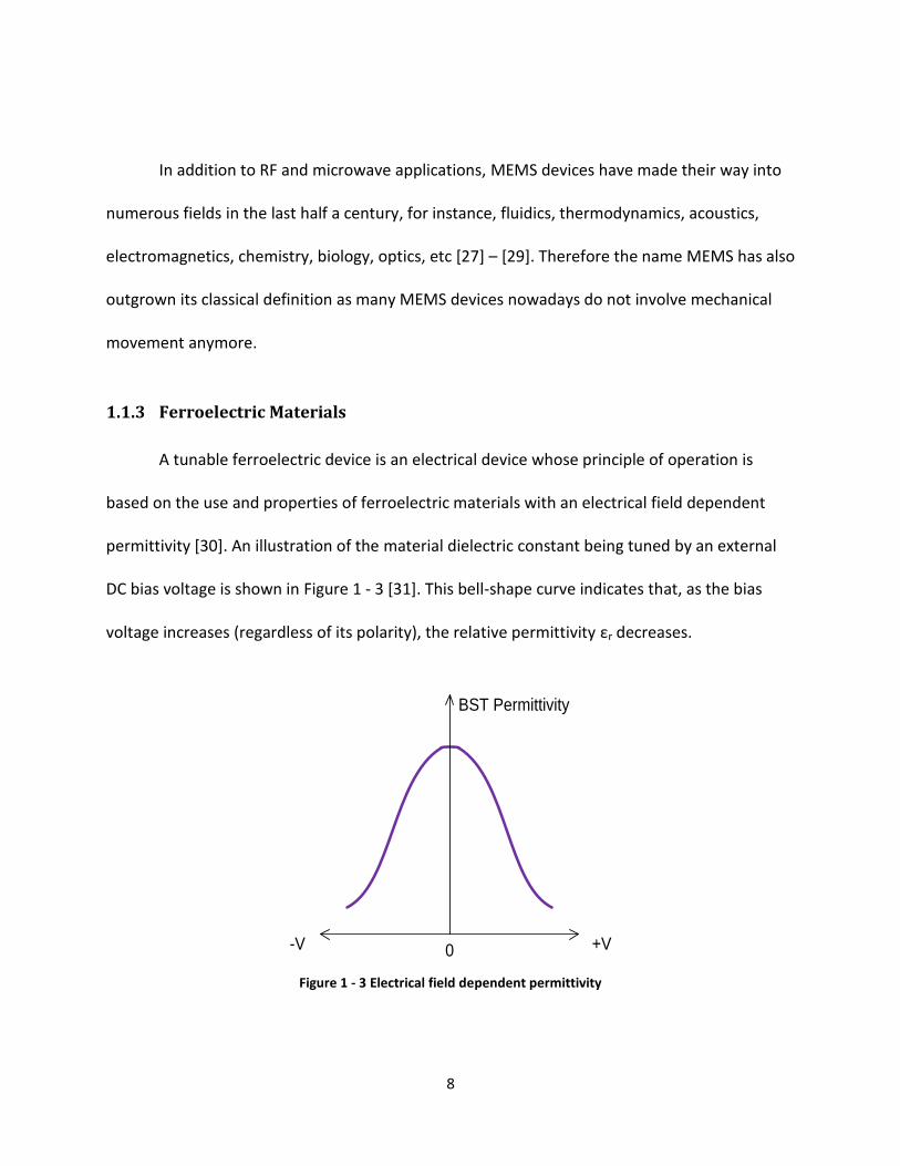
1.1.3 Ferroelectric Materials
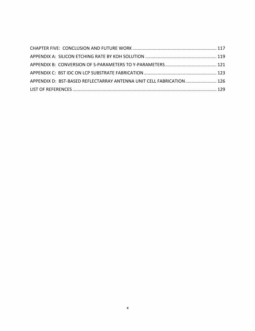
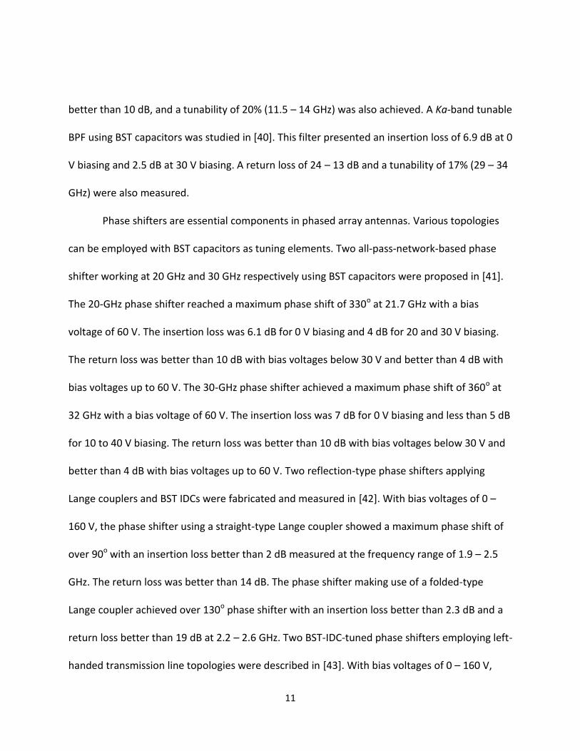
A tunable ferroelectric device is an electrical device whose principle of operation is
based on the use and properties of ferroelectric materials with an electrical field dependent
permittivity [30]. An illustration of the material dielectric constant being tuned by an external
DC bias voltage is shown in Figure 1 - 3 [31]. This bell-shape curve indicates that, as the bias
voltage increases (regardless of its polarity), the relative permittivity εr decreases.
Figure 1 - 3 Electrical field dependent permittivity
0 +V-V
BST Permittivity
9
Ferroelectric materials have been studied in the RF and microwave realms since the
1950s, yet only during the past two decades has enormous development progress been made.
Because of their material properties – high dielectric constant, good tunability, high breakdown
voltage and monolithic processing compatibility – ferroelectric materials, such as BST (BaxSr1-
xTiO3), PZT (PbZrxTi1-xO3), SBT (SrBi2Ta2O9), etc, are being used in various RF and microwave
devices [32]. Among those, BST is most frequently studied because of its overall advantages
compared with other ferroelectric materials. Hence the focus of this dissertation is going to be
placed on the BST material, specifically on its fabrication on flexible substrates.
BST being such a good candidate for tunable RF and microwave applications, a
significant amount of research has been conducted regarding the device implementation of BST
materials, for example, BST-based tunable capacitors, filters, phase shifters, and so on.
The very fundamental research efforts were made towards BST capacitors, since BST
material is primarily a dielectric. Both metal-insulator-metal (MIM) capacitor and inter-digital
capacitor (IDC) structures have been studied for capacitance, tunability, quality factor (Q),
linearity, etc. A BST capacitor with MIM structure was reported in [33]. Tunability of 71% (3.4:1)
was achieved with a bias voltage of 9 V at frequencies from 45 to 500 MHz, and a Q factor of
over 60 was obtained at 50 MHz for a 65 pF capacitor measured at 0V, which is comparable to
that of similar semiconductor based varactor diodes. The linearity of BST MIM capacitors was
improved in [34] by stacking multiple capacitors in series. The third-order intercept point at
input (IIP3) was improved by 16 dB. A tunability of 50% (2:1) was measured with a bias voltage
of 10 V, and a Q factor from 39 to 49 was obtained for a 1.4 pF capacitor at 1.3 GHz. The BST
10
varactors with MIM structure usually offer better tunability than those with IDC structure, while
the fabrication complexity of BST IDC is usually lower. A BST IDC with a tunability of 21% at a
30-V maximum bias voltage was reported in [35]. Its capacitance was measured from 0.78 to
0.62 pF and a Q factor was measured from 17.1 to 25 with 0 to 30 V bias voltages at 2.5 GHz. A
more recently research on a BST IDC working from low frequency to 50 GHz was presented in
[36]. This capacitor exhibited a tunability of 63% with a 5 V DC bias. At 0 bias it has a
capacitance of 0.2 pF and a Q factor of 50 around 30 GHz.
Other tunable RF and microwave devices based on BST capacitors have also been
studied extensively. Tunable filters play a substantial role in a variety of applications in modern
communication systems. For this reason, they have been investigated for different frequency
bands from VHF to Ka-band and above [37] – [40]. A low-pass filter (LPF) and a band-pass filter
(BPF) applying BST MIM capacitors and other lumped elements were studied in [37]. For the
LPF, an insertion loss of 2 dB, a return loss better than 7 dB, and a tunability of 40% (120 – 170
MHz) with tuning voltages of 0 – 9 V were measured up to 500 MHz. For the BPF, an insertion
loss of 3 dB, a return loss better than 7 dB, and a tunability of 57% (176 – 276 MHz) with tuning
voltages of 0 – 6 V were obtained. An S-band BPF applying BST IDC structure was investigated in
[38]. Measurements showed an insertion loss of 5.1 dB at 0 V biasing, 3.3 dB at 200 V biasing
and a return loss better than 13 dB for all bias voltages. A tunability of 16% (2.44 – 2.88 GHz)
with up to 200 V biasing was also obtained. A Ku-band miniaturized (2mm by 6mm) slow-wave
tunable BPF utilizing BST IDC structure is demonstrated in [39]. This BPF exhibited an insertion
loss of 5.4 dB at 0 V biasing and 3.3 dB at 30 V biasing. The return loss was measured to be
11
better than 10 dB, and a tunability of 20% (11.5 – 14 GHz) was also achieved. A Ka-band tunable
BPF using BST capacitors was studied in [40]. This filter presented an insertion loss of 6.9 dB at 0
V biasing and 2.5 dB at 30 V biasing. A return loss of 24 – 13 dB and a tunability of 17% (29 – 34
GHz) were also measured.
Phase shifters are essential components in phased array antennas. Various topologies
can be employed with BST capacitors as tuning elements. Two all-pass-network-based phase
shifter working at 20 GHz and 30 GHz respectively using BST capacitors were proposed in [41].
The 20-GHz phase shifter reached a maximum phase shift of 330o at 21.7 GHz with a bias
voltage of 60 V. The insertion loss was 6.1 dB for 0 V biasing and 4 dB for 20 and 30 V biasing.
The return loss was better than 10 dB with bias voltages below 30 V and better than 4 dB with
bias voltages up to 60 V. The 30-GHz phase shifter achieved a maximum phase shift of 360o at
32 GHz with a bias voltage of 60 V. The insertion loss was 7 dB for 0 V biasing and less than 5 dB
for 10 to 40 V biasing. The return loss was better than 10 dB with bias voltages below 30 V and
better than 4 dB with bias voltages up to 60 V. Two reflection-type phase shifters applying
Lange couplers and BST IDCs were fabricated and measured in [42]. With bias voltages of 0 –
160 V, the phase shifter using a straight-type Lange coupler showed a maximum phase shift of
over 90o with an insertion loss better than 2 dB measured at the frequency range of 1.9 – 2.5
GHz. The return loss was better than 14 dB. The phase shifter making use of a folded-type
Lange coupler achieved over 130o phase shifter with an insertion loss better than 2.3 dB and a
return loss better than 19 dB at 2.2 – 2.6 GHz. Two BST-IDC-tuned phase shifters employing left-
handed transmission line topologies were described in [43]. With bias voltages of 0 – 160 V,
12
maximum phase shifters of 413o for design-I and 412o for design-II were obtained; maximum
insertion losses of 10.3 dB or 8 dB and return loss better than 15 dB or 10 dB were also
measured at 10 GHz for design-I and design-II respectively. A phase shifter consisting of a CPW
line periodically loaded with BST IDC was described in [44]. A phase shift of 360o was achieved
with 40 V biasing at 30 GHz, and insertion losses of below 5 dB and around 15 dB were also
measured for bias voltages of 40 V and 0 V respectively. No return loss data was reported in the
study. A similar phase shifter applying the same topology was also reported in [45]. This phase
shift was characterized up to 30 GHz, with a phase shift of 310o measured with a 35 V bias
voltage at 30 GHz, a maximum insertion loss of 3.6 dB and a return loss better than 12 dB.
1.1.4 A Comparison of the Current Available Tunable Technologies
Since each tunable technology has its pros and cons, a comparison of these technologies
is shown in Table 1 - 1 [1] [2] [46].
13
Table 1 - 1 Comparison of current available tunable technologies
Varactor Diode MEMS Ferroelectric
Tunability High High Moderate to High
Tuning Speed Fast Slow Fast
Continuous Tuning Continuous Discrete (typically) Continuous
Control Voltage Low High Low to High
Loss Moderate Low Moderate
Power Consumption Poor Excellent Excellent
Reliability Good Poor Excellent
Cost Moderate Moderate Low
Packaging Requirement Need Need No Need
1.2 Flexible Electronics
Flexible electronics, as the name implies, mean electronic circuitries and devices
fabricated on flexible substrates with the benefit that they can conform to a desired shape or
flex before, during or after their use. The very first device was a single-crystalline silicon solar
cell that was demonstrated in the 1960’s. Since then, the flexible electronics industry has
become a wide-open area and has been expanding rapidly [47].
14
A few recent applications of flexible electronics can be found in the free e-book “A
Foldable World” [48]. In 2003, the world’s first polymer-based transistor completely produced
using continuous mass printing was presented at the Institute for Print and Media Technology
at Chemnitz University of Technology. Later, the first fully printed ring oscillator on transparent
and flexible substrate applying seven stages using the same printing technology was also
created by the same institute [49]. Though the performance of either the transistors or the ring
oscillators was not yet comparable to the semiconductor counterparts, the breakthrough of this
technology still attracted a lot of attentions. In 2007, fully transparent and medically flexible
nanowire transistors (NWTs) on plastic substrates were reported in [50]. These devices
exhibited high-performance n-type transistor characteristics with about 82% optical
transparency. In 2008, a novel way of collecting solar energy using a flexible nano-antenna
electromagnetic collector (NEC) was developed in [51]. These nano-antennas can take in
infrared energy that is from both sunlight and the earth’s heat and convert it with higher
efficiency than conventional solar cells. In later years, more advanced flexible electronics have
been reported by both academic and industrial research institutes. Sony demonstrated for the
first time a 4.1-inch super-thin (about 80 µm thick) organic light-emitting diode (OLED) display
with a 432 × 240 resolution (121 ppi) and a 1000:1 contrast ratio. This display was so thin that it
could be wrapped around a pencil while continuing to display images and videos [52]. Bio-
compatible LED arrays capable of bending, stretching and being implanted under the skin using
traditional semiconductor GaAs (Gallium Arsenide) and conventional metals were introduced in
[53]. This technology can be used to activate drugs, monitor medical conditions or perform
15
other biomedical tasks inside human bodies. A thin, flexible secondary Li-ion paper battery
applying carbon nanotube (CNT) thin films was also reported in [54]. This battery was only 300-
µm-thick, yet exhibited robust mechanical flexibility (being able to bend down to less than 6
mm) and high energy density (108 mWh/g). Tests showed that this new prototype was capable
of recharging up to 300 times without failure. All-printed and roll-to-roll-printable 1-bit radio
frequency identification (RFID) tags on plastic foils were demonstrated in [55]. Operating at
13.56 MHz, these RFID tags could generate 102.8 Hz of clock signal as the tags approached the
RFID reader.
1.2.1 Materials and Fabrication Techniques for Flexible Electronics
Popular flexible substrates that serve as replacements for conventional rigid substrates
include, but are not limited to, thin glass, organic polymers (plastics) and metal foil [47]. Thin
glass is the standard substrate in current flat panel display technology; organic polymers such
as polyethylene terephthalate (PET), polyethylene naphthalate (PEN), and polyimide (PI), are
being researched to bear silicon-based devices; metal foil substrates are very attractive for
emissive or reflective displays. A number of requirements need to be met in the following areas
so that these materials can be used as the substrate for flexible electronics: surface roughness,
mechanical properties, chemical properties, thermal and thermo-mechanical properties, optical
properties, electrical and magnetic properties, etc.
Of the options discussed above, the liquid crystalline polymer (LCP), a class of aromatic
polyester polymer, exhibits unique electrical, physical and chemical properties, which makes it
16
favorable for RF and microwave applications. Section 1.2.2 will talk about different applications
of this substrate.
Two industrial approaches are being used for flexible electronics manufacturing: (1)
transfer of a complete device or circuit to flexible substrates, and (2) direct fabrication of
circuitry on flexible substrates. Either approach requires all components to comply with
bending to a certain extent without compromising performance.
For the transfer approach, the whole device or circuit is first fabricated on a traditional
rigid substrate such as a silicon or GaAs wafer, then diced and wire-bonded onto a flexible
substrate. Wire-bonding has long been used in research and industry. This method provides
high-performance devices comparable to those on rigid substrates. However it suffers from
small surface area coverage, high cost and high-frequency operation restriction resulting from
the inductive effects of the bond wires.
The direct fabrication approach is also used in many applications. It allows large-area
mass production with all components fabricated directly onto the flexible substrate. Not all
flexible substrates are compatible with the existing microfabrication processes, mostly because
of the high-temperature related procedures. Innovative techniques are being investigated,
including additive printing of each layer of the devices, the printing of masks and etching, etc.
1.2.2 LCP State-of-the-art Applications
LCP material has drawn a lot of attention in the RF and microwave field because of its
low relative dielectric constant, low dissipation factor and low lamination temperature. Recent
17
research and development have shown that LCP is probably the best polymer for multilayer
packaging, because while it is flexible, lighter and much less expensive, it also exhibits device
performance comparable to traditional metal and ceramic hermetic packages.
Immersion tests of patch antennas fabricated on three different flexible substrates were
carried out in [56]. Results showed that the LCP substrate was superior to the other two low-
moisture-absorption-substrates tested, since it showed no measureable changes in weight or
antenna resonance frequency after up to 16-days of submersion in water. It has also been
found that LCP materials can be used as a low-cost substitutes for standard hermetic materials
for monolithic microwave integrated circuit (MMIC) packaging applications in RF, microwave
and millimeter wave (MMW) frequencies. The packaging capability of the LCP substrates was
investigated as early as 1995 [57]. It was concluded that the packaged devices can be made
hermetic and the weight was only half to one fourth of the ceramic-packaged devices. The cost
was about one fifth of that for ceramic packaging. Recent research has showed even more
capacities of this substrate. LCP substrates with laser-micromachined cavities were used as the
packaging substrate for MMIC and RF MEMS devices. Results measured up to 40 GHz showed
that no significant difference was found between the devices with and without LCP packaging.
For millimeter wave (MMW) applications, LCP substrate was studied as the substrate/packaging
material for a low-loss integrated waveguide (IWG), a microstrip line-to-IWG transition and an
IWG bandpass filter (BPF) in [59]. The insertion loss was measured at 0.12 dB/mm for the IWG
and 0.14 dB for the microstrip line-to-IWG transition at 60 GHz. The three-pole BPF with a
center frequency of 61.1 GHz achieved a 3-dB bandwidth of 13.4%, an insertion loss of 1.8 dB
18
and a rejection of greater than 15 dB. For all the applications demonstrated, LCP substrate has
been proven as an excellent RF and microwave substrate and a system-level packaging
material.
Various antennas and power amplifiers on LCP substrates were also studied and
compared with those on rigid substrates. An RFID tag antenna covering both the European (866
MHz – 868 MHz) and North American (902 MHz – 928 MHz) RFID UHF frequency bands was
fabricated on 4-mil-thick LCP substrate in [60]. The measured return loss was better than 10 dB,
which was in agreement with the simulation. Dual-frequency (14 GHz and 35 GHz), dual-
polarization microstrip antenna arrays were demonstrated in [61]. The return losses for both
frequencies were better than 15 dB, and the measured bandwidths agreed with simulation
results. A CPW-fed micromachined stacked patch antenna was presented in [62]. The LCP
material was used to mechanically support and form cavities to protect the radiating and
parasitic patch elements. Measurement results showed a gain of 7.6 dBi and a bandwidth of
44%. A flexible ultra-wideband (UWB) elliptical slot antenna on LCP substrate was investigated
for breast cancer detection in [63]. This CPW-fed antenna was capable of detecting small
tumors with a size below 2 mm. The preliminary results of using a conformal 3-element array
showed very promising sensitivity enhancement. A 6 – 18 GHz push-pull power amplifier (PA)
module on a LCP substrate was studied in [64]. With very low even-order distortions, this PA
showed a P1dB power of 31 dBm and a 2nd order harmonic distortion reduction of over 20 dB
compared to a single PA throughout the passband.
19
1.3 Tunable and Flexible – The Newly-mingled Field
As both tunability and flexibility are much desired features, many research groups have
invented new techniques that can realize this combination in the RF and microwave regions.
The following attempts are the most cutting-edge accomplishments and thus are not
commercially available yet.
One simple concept is to mount tunable components onto a flexible substrate to realize
both tunability and flexibility. An example can be found in [65], in which a low-loss and
compact-sized X-band analog tunable filter was fabricated and measured on a flexible LCP
substrate. Tunable BST capacitor chips were surface-mounted onto the substrate using silver
epoxy and ribbon bond. This design was flexible and about 50% smaller than a conventional
open-loop resonator filter, and yet achieved a tuning of 12%, a return loss of better than 10 dB
and an insertion loss of 1.8 – 5.5 dB. However, as mentioned in the previous section, this
method has limitations, such as the extent of flexibility and the operation frequency.
Specifically, the bond wires used in the circuit will add in a considerable inductive effect as the
operation frequency increases.
Another remarkable approach is based on silicon-nanomembrane (SiNM), as described
in detail in [66]. Silicon based devices, such as diodes (varactors) and transistors, can first be
fabricated on the silicon nanomembrane, which is an elastically strain-sharing multilayer
structure consisting of Si-SiGe-Si layers. This multilayer structure is originally positioned on a
buried oxide (BOX) layer on a silicon wafer. By removing the BOX layer, the SiNM layer with the
device is released from the silicon wafer, and can then be transferred onto a foreign substrate,
20
including a flexible substrate. For instance, SiNM-based PIN diodes on flexible plastic substrates
were demonstrated in [67]. Measurement showed typical rectifying characteristics. An insertion
loss of less than 1.7 dB and isolation better than 20 dB were achieved from DC up to 5 GHz at
low bias conditions. This approach is an innovation of the monolithic fabrication of silicon-
based devices. Nevertheless, the possibility of large-scale fabrication is still under investigation.
Another notable method is to take advantage of the packaging capability of flexible
materials to realize reconfigurable system-on-package (SOP). In [68], two reconfigurable RF
MEMS phased array antennas were integrated into a SOP on LCP substrates. LCP substrates, in
this case, were used as the RF substrates as well as the packaging materials. Working at 14 GHz,
both antennas (one using a single layer SOP and the other using a multilayer SOP) exhibited low
loss characteristics and were able to achieve 12o of beam steering. In [69], tunable frequency-
selective surfaces (FSS) and electromagnetic-bandgap (EBG) structures on rigid-flex Kapton
substrates were fabricated using a newly-developed MEMS process. Kapton substrate is all
dielectric and after the special treatment is semi-flexible. The FSS switching between Ku-band
and Ka-band showed center frequencies of 17.8 GHz and 21.3 GHz at down-state and up-state,
respectively. The measured ±90o bandwidth for the EBG was 1.91% (bias on) and 1.29% (bias
off). Another example demonstrated that MEMS sensors, a flow sensor and a tactile sensor, can
be fabricated directly onto the flexible LCP substrate [70]. The flow sensor tested with flow
rates from 0 to 20 m/s showed an expected velocity-squared relationship. The tactile sensor
displayed a hysteretic behavior originally, which disappeared after flexing the device for a few
times.
21
BST-based tunable capacitors have also been made on copper foil with the use of
controlled oxygen pressure [71] or in a nearly inert atmosphere [72] during annealing. The core
of both techniques is to prevent copper from oxidazing in the high temperature annealing
process. The drawback for this technique is that copper is not a typical RF and microwave
substrate, therefore the applications for BST thin film on copper foil are limited.
The use of liquid crystal as the dielectric material of a tunable capacitor working in RF
and microwave frequencies was also presented in [73]. With a control voltage of 5 V, a quality
factor of 310 was measured at 4 GHz, and a tunability of 25.4% was obtained at 5 GHz. This
approach is suitable for preparing tunable devices on flexible substrates, especially for
transparent applications.
In this work, the possibility of BST thin film on LCP substrate is investigated, and a new
transfer technique incorporating wafer-bonding and substrate-etching is proposed. This will be
discussed in detail in Chapter 2.
1.4 Dissertation Outline
This dissertation consists of five major sections.
The first chapter is an introduction to tunable and flexible electronics. It covers the
motivation of this work, and the state-of-the-art research in tunable components, flexible
devices, and smart flexible electronics.
22
Chapter 2 is everything about BST – Barium Strontium Titanate. Material properties,
deposition techniques, analytical techniques and a new transfer technique are all discussed in
detail.
Chapter 3 talks about our research of a new transfer technique to realize BST-based
tunable capacitors on flexible LCP (liquid crystalline polymer) substrates. Simulation,
fabrication, measurement, results and detailed discussions are presented.
Chapter 4 focuses on our primary study of a BST-based reflectarray antenna. Unit cell
optimization is studied and the results are verified by either simulation or measurement or
both.
This dissertation is concluded in chapter 5. Future work based on this research is also
proposed.
23
CHAPTER TWO: BST – A SMART MATERIAL
BST, Barium Strontium Titanate, is considered a smart material mainly because of its
electric-field-dependent permittivity. It also has other good qualities such as high permittivity
and a high breakdown voltage. This chapter will focus on different aspects of this material,
including physical and electrical properties, fabrication methods, material characterization and
a new transfer technique that makes it possible to have BST thin films on flexible LCP
substrates.
2.1 BST Material Properties
2.1.1 Ferroelectric Phenomenology
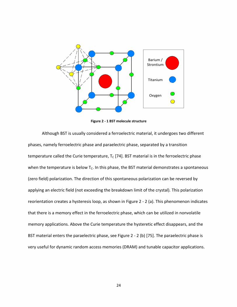
Ba1-xSrxTiO3 is a continuous solid solution between two basic substances, BaTiO3 and
SrTiO3. Since both of them have the perovskite crystal structure, BST naturally inherited the
same structure. Figure 2 - 1 shows a BST perovskite crystalline lattice, where a large Barium (Ba)
or Strontium (Sr) atom (red) occupies the center position of the cube, eight Titanium (Ti) atoms
(blue) sit in the corners, and twelve Oxygen (O) atoms (green) take the midpoint of each edge.
The yellow atoms are oxygen ions from adjacent molecules that share the titanium ion in that
corner.
24
Figure 2 - 1 BST molecule structure
Although BST is usually considered a ferroelectric material, it undergoes two different
phases, namely ferroelectric phase and paraelectric phase, separated by a transition
temperature called the Curie temperature, TC [74]. BST material is in the ferroelectric phase
when the temperature is below TC. In this phase, the BST material demonstrates a spontaneous
(zero field) polarization. The direction of this spontaneous polarization can be reversed by
applying an electric field (not exceeding the breakdown limit of the crystal). This polarization
reorientation creates a hysteresis loop, as shown in Figure 2 - 2 (a). This phenomenon indicates
that there is a memory effect in the ferroelectric phase, which can be utilized in nonvolatile
memory applications. Above the Curie temperature the hysteretic effect disappears, and the
BST material enters the paraelectric phase, see Figure 2 - 2 (b) [75]. The paraelectric phase is
very useful for dynamic random access memories (DRAM) and tunable capacitor applications.
Barium /Strontium
Titanium
Oxygen
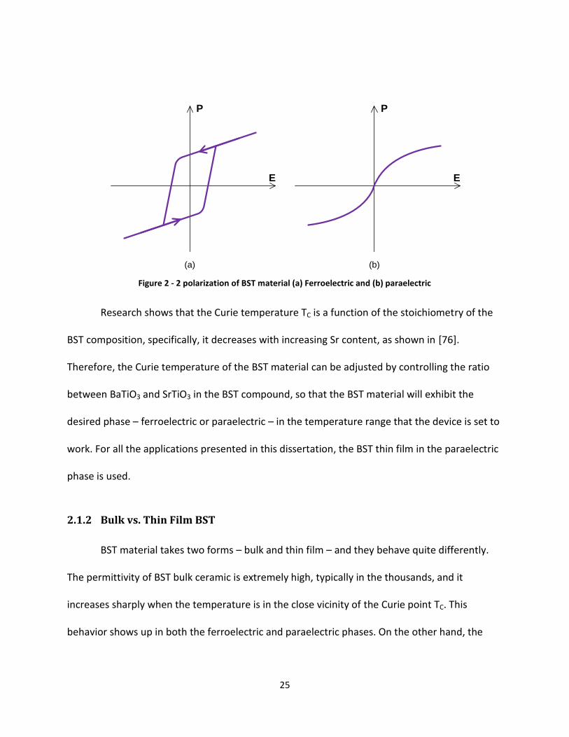
25
Figure 2 - 2 polarization of BST material (a) Ferroelectric and (b) paraelectric
Research shows that the Curie temperature TC is a function of the stoichiometry of the
BST composition, specifically, it decreases with increasing Sr content, as shown in [76].
Therefore, the Curie temperature of the BST material can be adjusted by controlling the ratio
between BaTiO3 and SrTiO3 in the BST compound, so that the BST material will exhibit the
desired phase – ferroelectric or paraelectric – in the temperature range that the device is set to
work. For all the applications presented in this dissertation, the BST thin film in the paraelectric
phase is used.
2.1.2 Bulk vs. Thin Film BST
BST material takes two forms – bulk and thin film – and they behave quite differently.
The permittivity of BST bulk ceramic is extremely high, typically in the thousands, and it
increases sharply when the temperature is in the close vicinity of the Curie point TC. This
behavior shows up in both the ferroelectric and paraelectric phases. On the other hand, the
P
E
P
E
(a) (b)
26
permittivity of BST in the thin film form is much lower, usually in the hundreds, and there is no
sharp peak observed with temperature variation. An example is shown in [77].
For the BST thin film particularly, the permittivity also varies with film thickness, as
shown in [78]. A thicker film provides higher permittivity as well as higher tunability. Therefore,
a certain thickness is needed in order to reach a specific value for both the permittivity and the
tunability.
In this dissertation we are studying BST thin films on LCP substrates and sapphire
substrates for applications in tunable capacitors, phase shifters and reflectarray antennas.
2.1.3 BST Thin Film Electrical Properties
Originated from the perovskite crystal structure, the BST thin film possesses a few
unique electrical properties that make it an excellent candidate for RF and microwave
applications. Some of these properties are listed below.
1. High permittivity.
Thin film BST permittivity is usually in the hundreds, depending on the BST composition
(Ba:Sr ratio), the thickness of the film and the level of crystallization. A better crystallized BST
thin film can be obtained by optimizing the deposition conditions, such as substrate
temperature, annealing temperature, ambient pressure, gas mixture, etc, during both
deposition and annealing processes. Thicker film and better crystallization ensures higher
27
permittivity, and the higher permittivity allows smaller device dimensions and therefore a
compact design.
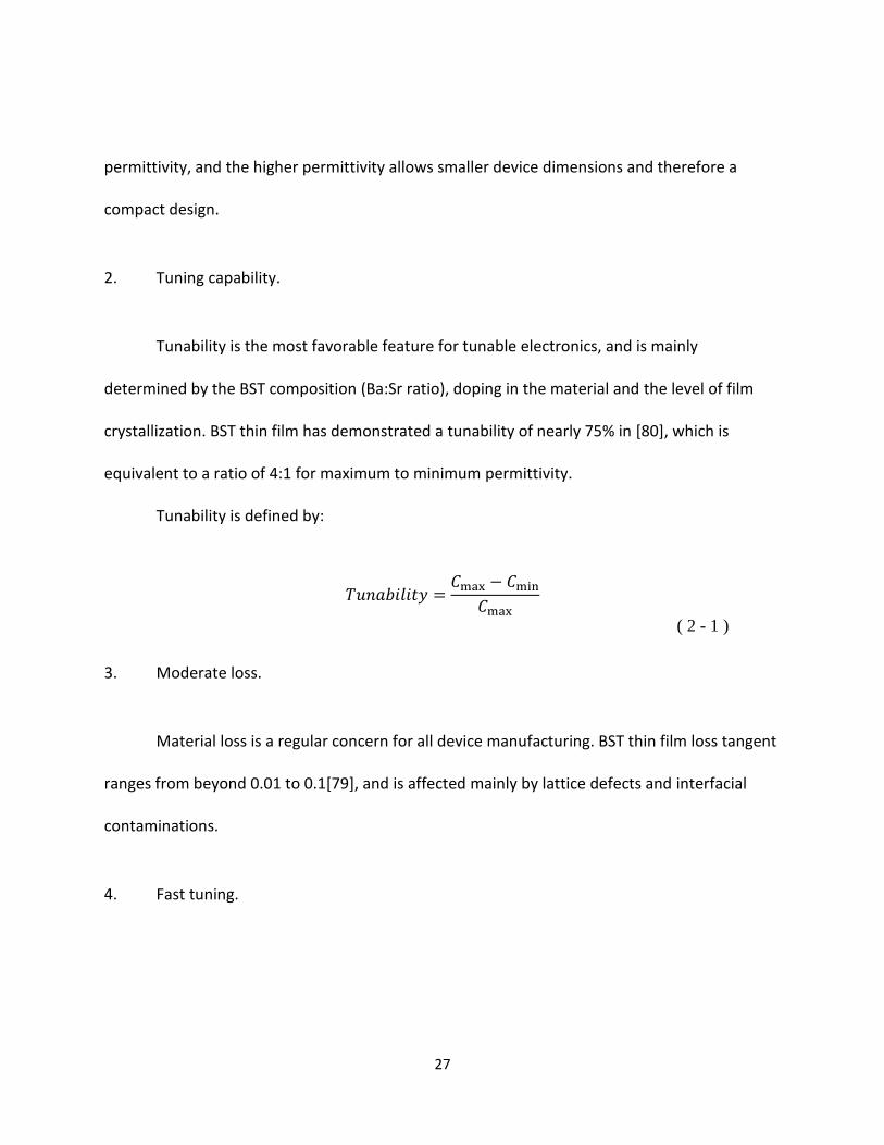
2. Tuning capability.
Tunability is the most favorable feature for tunable electronics, and is mainly
determined by the BST composition (Ba:Sr ratio), doping in the material and the level of film
crystallization. BST thin film has demonstrated a tunability of nearly 75% in [80], which is
equivalent to a ratio of 4:1 for maximum to minimum permittivity.
Tunability is defined by:
( 2 - 1 )
3. Moderate loss.
Material loss is a regular concern for all device manufacturing. BST thin film loss tangent
ranges from beyond 0.01 to 0.1[79], and is affected mainly by lattice defects and interfacial
contaminations.
4. Fast tuning.
28
BST tuning originates from its dipole reorientation, thus its tuning speed is as fast as the
rate of its electric polarization, which is normally in the picoseconds range. This is critical for
applications that require fast response, like multipliers and phase shifters.
5. Continuous tuning
The dipole-reorientation-originated tuning is also continuous. Therefore, with a proper
bias voltage, the BST permittivity can reach any value between the minimum and maximum of
that particular film.
6. Non-linear behavior
The non-linear relationship between the electric field (bias voltage) and the permittivity,
as shown in Figure 1 - 3, makes it possible for the BST thin film to be used in frequency
conversion devices, such as multipliers and mixers.
7. High power handling capacity
High breakdown voltage of more than 2×10⁶ V/cm has been reported in [80]. This
ensures that BST thin film can handle large RF signals and thus can be used in high power
devices.
8. Low power consumption or leakage current
29
Leakage current is the main cause for power consumption. Devices made from BST thin
films exhibit low leakage current density in the order of 10-8 A/cm2 [81].
9. High frequency device feasibility
BST thin film based devices are compatible with the existing semiconductor
manufacturing process. This lack of a packaging requirement enables the integration with other
parts of the circuit components, thus leading to low cost applications in RF and microwave even
millimeter wave (MMW) frequencies.
2.2 BST Deposition Techniques
The most commonly used BST deposition techniques in research and in industry are the
RF magnetron sputter deposition, pulsed laser deposition (PLD), sol-gel, chemical vapor
deposition (CVD) including metal-organic chemical vapor deposition (MOCVD) and combustion
chemical vapor deposition (CCVD). Since RF magnetron sputtering is employed in this work, it is
explained here in detail. A brief description of the other processes is also given in the following
sections.
2.2.1 RF Magnetron Sputter Deposition
Sputter deposition falls into the physical vapor deposition (PVD) category. It is a process
of depositing thin films by ejecting material atoms or molecules from a source material onto a
substrate using atom bombardment, which is excited by accelerating ionized neutral gas

30
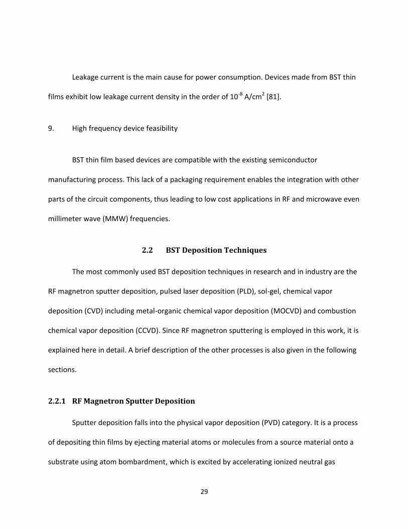
molecules in a vacuum environment. A typical system is illustrated in Figure 2 - 3 (a) [82]. The
source material is also called a ‘target’, also shown in Figure 2 - 3 (b), which is mounted in a
‘gun’ located at the bottom of the system.
31
Figure 2 - 3 An RF sputtering system, (a) diagram, (b) targets, and (c) the inside picture of a 3-gun sputtering system
The use of a magnetron – by placing a magnet below the target in the gun – can
considerably improve the deposition rate. Both DC power and RF power can be used in the
32
magnetron sputtering system. DC magnetron sputtering is only good for conducting materials
while RF magnetron sputtering can be used for both conducting and non-conducting materials.
The top view of an open magnetron sputtering system with 3 guns is shown in Figure 2 - 3 (c).
This system is capable of loading up to 3 different materials in the same chamber. Therefore, 3
different thin films or the combination of any of them may be deposited in the same vacuum.
When the RF magnetron sputtering process starts, the magnetic field traps a good
number of free electrons right above the target. This greatly increases the chance of the neutral
gas molecules getting ionized by these electrons. The positively charged ions (ionized neutral
gas molecules) are then attracted towards the target by the cathode connected to gun and
strike the target in an accelerated fashion. The target is then eroded by these ions through
momentum transfer and the source material is ejected as neutral particles – in the form of
individual atoms and/or clusters of atoms or molecules – traveling in a straight line onto the
substrate. Thin film deposition is achieved as a result.
An AJA ATC 1800 magnetron sputtering system is used to deposit BST thin films in this
work. With three guns and two power sources, one DC and one RF, this system can deposit
three different types of thin films alternatively or a combination of two materials.
2.2.2 Pulsed Laser Deposition PLD
PLD is also classified as a PVD process. It utilizes a focused pulsed laser beam with high
power to strike a material target in such a way that the material is vaporized and deposited
onto a substrate [83]. Although a series of events occur during this whole process, the
33
deposited thin film keeps the exact same chemical composition as the target material. The
uniqueness of this deposition is that the energy source (laser) is placed outside the chamber,
thus the operating pressure can be controlled in a wide range from ultra high vacuum (UHV) to
a fraction of the atmosphere pressure. Additionally, film thickness can be controlled by varying
the number of laser pulses.
Detailed BST thin film deposition parameters using PLD technique can be found in [84].
2.2.3 Sol-gel
The sol-gel process is a wet-chemical deposition technique that employs a ‘sol’ (usually a
colloidal solution) as the precursor to evolve towards the formation of a solid ‘gel’ phase [85]. A
thin film can be obtained by spin-coating or dip-coating a substrate. Other forms, such as fiber,
powder, porous and dense materials, can also be produced by appropriate treatment. A drying
or thermal procedure is often needed afterwards for further poly-condensation or mechanical
property and stability enhancement.
A detailed description of BST thin film deposited by the sol-gel process can be found in
[86].
2.2.4 Chemical Vapor Deposition CVD
The CVD process makes use of the reaction and/or decomposition of volatile precursors
in gaseous state to produce the thin film when they pass over or come into contact with a
heated substrate. CVD is extremely versatile and can be used to process a wide range of metals
34
and ceramics. Substrate temperature, chamber pressure and precursor concentration are the
control parameters that will yield the desired thin film product [87].
The CVD process can be further classified into many different categories, among which
MOCVD [88] and CCVD [89] are being used for BST thin film deposition.
2.3 BST Analytical Techniques
After a BST thin film is deposited onto a substrate, both its material composition and the
degree of crystallization need to be characterized.
In this work, the atomic ratio of Ba:Sr:Ti:O is analyzed by a General IONIX 1.7 MU
Tandetron Rutherford Backscattering Spectroscopy (RBS) system, whose primary application is
to obtain a quantitative composition of a material and a depth profiling of individual elements.
This is accomplished by measuring the backscattering of a beam of high energy ion – typically
helium ions with energy of a few MeV – impinging on a thin film sample. The detection limits
are 1-10 atomic percent for low atomic number elements and 0-100 parts per million (ppm) for
high atomic number elements, which indicates a better sensitivity for heavier elements.
An example of the measured data of a BST thin film using RBS is shown in Figure 2 - 4.
The line in black is the experimental spectrum or the raw data, and the line in red is the fit for
elemental profiles generated by computer simulation. As we can see that the curve exhibits a
staircase structure, which is typical for RBS measurement. Each step is associated with one of
the elements in the thin film or the substrate. The X-axis of the plot is associated with the
energy of the backscattered particles. The front edge position of each step defines the type of
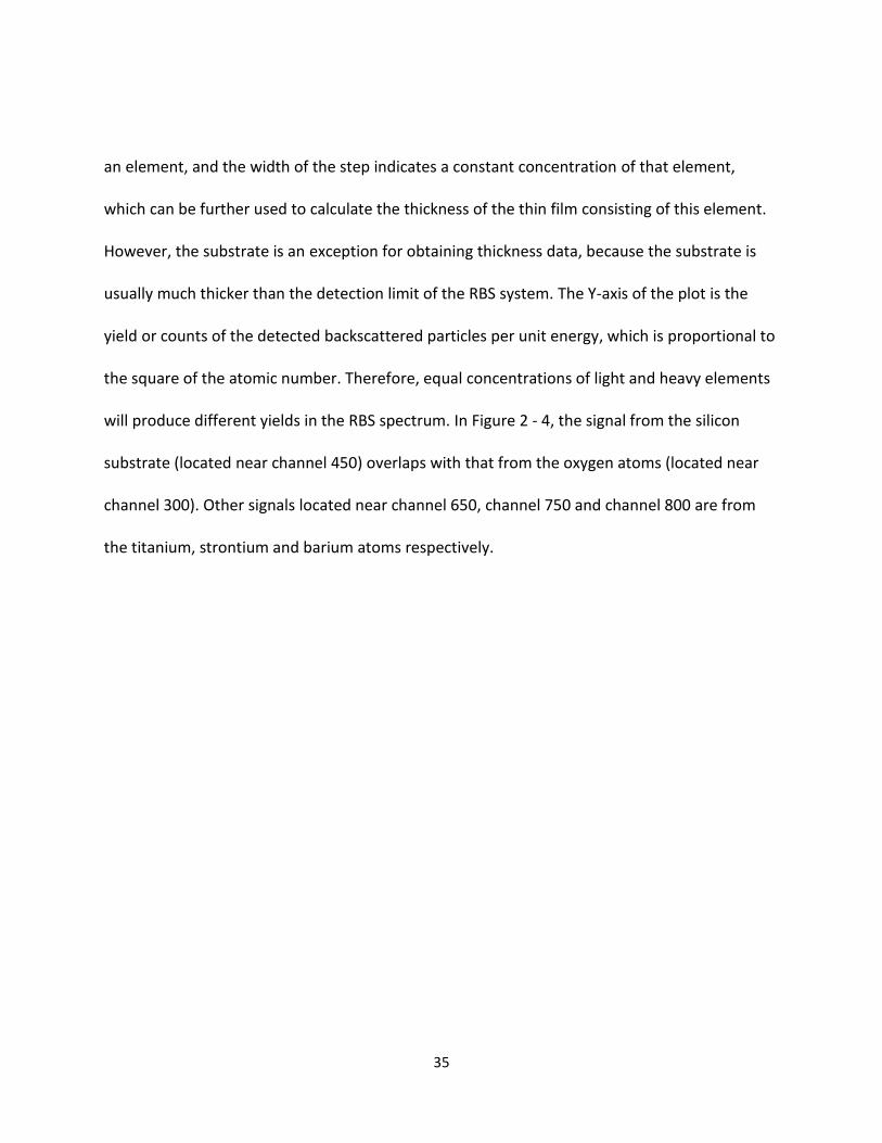
35
an element, and the width of the step indicates a constant concentration of that element,
which can be further used to calculate the thickness of the thin film consisting of this element.
However, the substrate is an exception for obtaining thickness data, because the substrate is
usually much thicker than the detection limit of the RBS system. The Y-axis of the plot is the
yield or counts of the detected backscattered particles per unit energy, which is proportional to
the square of the atomic number. Therefore, equal concentrations of light and heavy elements
will produce different yields in the RBS spectrum. In Figure 2 - 4, the signal from the silicon
substrate (located near channel 450) overlaps with that from the oxygen atoms (located near
channel 300). Other signals located near channel 650, channel 750 and channel 800 are from
the titanium, strontium and barium atoms respectively.
36
Figure 2 - 4 Sample data of an RBS measurement
BST crystallization is examined by a Rigaku D/MAX X-Ray Diffraction (XRD) system in this
study, which can determine the crystal structure and lattice parameters of a crystalline
material. This is achieved by measuring the intensity of X-rays beams diffracted by the thin film
under investigation. According to Bragg’s Law, diffraction occurs only when the X-ray beam is
incident at a certain angle that causes constructive interference. Therefore by plotting the
intensity of the diffracted X-ray beams versus the incident angle, crystal orientation can be
identified. Furthermore, by comparing the measured data with that in a database, an unknown
crystalline phase and orientation of a sample can be labeled. An example of an XRD
measurement is shown in Figure 2 - 5. The X-axis is associated with the angle of the incident X-
200 400 600 800
Channel
0
5
10
15
20
25
30N
orm
aliz
edY
ield
0.5 1.0 1.5 2.0
Energy (MeV)
BST on Silicon
Comp Ba 7.7 Sr 10.5 Ti 25.8 O 56.0
37
ray, 2θ to be exact. The Y-axis is the intensity of the X-ray detected. The strongest peak near 2θ
= 31 corresponds to a crystal orientation of <110> for BST thin film. The rest of the peaks
associated with other crystal orientations are considerably smaller compared to the <110>
peak, which indicates that this thin film is primarily consisting of crystal orientation <110>.
Figure 2 - 5 Sample data of an XRD measurement
2.4 BST Transfer Technique
BST material quality (permittivity, tunability, loss, etc) is largely determined by its
crystallinity level, i.e. a high degree of crystallization lead to a good thin film quality. The
crystalline structure can be achieved by a post-deposition annealing. A high temperature above
700oC is usually required for such a process. On the other hand, most flexible substrates have a
melting point well below 700oC. For instance the melting temperature for an LCP substrate is
315oC. This creates a difficult dilemma that prevents the BST thin film from being deposited and
annealed directly on the flexible substrates.
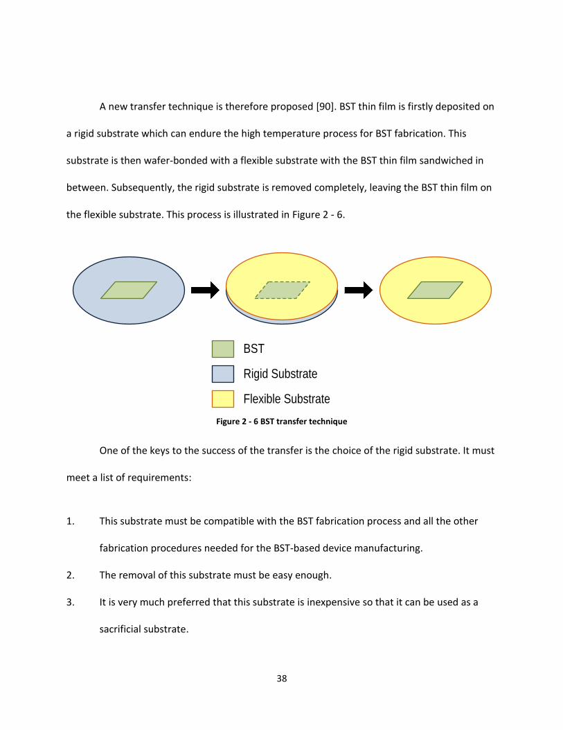
38
A new transfer technique is therefore proposed [90]. BST thin film is firstly deposited on
a rigid substrate which can endure the high temperature process for BST fabrication. This
substrate is then wafer-bonded with a flexible substrate with the BST thin film sandwiched in
between. Subsequently, the rigid substrate is removed completely, leaving the BST thin film on
the flexible substrate. This process is illustrated in Figure 2 - 6.
Figure 2 - 6 BST transfer technique
One of the keys to the success of the transfer is the choice of the rigid substrate. It must
meet a list of requirements:
1. This substrate must be compatible with the BST fabrication process and all the other
fabrication procedures needed for the BST-based device manufacturing.
2. The removal of this substrate must be easy enough.
3. It is very much preferred that this substrate is inexpensive so that it can be used as a
sacrificial substrate.
BST
Rigid Substrate
Flexible Substrate

39
In this work, a test grade silicon wafer with <100> crystalline orientation is used as the
rigid substrate. It is available at less than $10/pc. Moreover, silicon etching is a matured process
in the semiconductor industry, and the etching rate can reach as high as several
microns/minute, as seen in Appendix A [91].
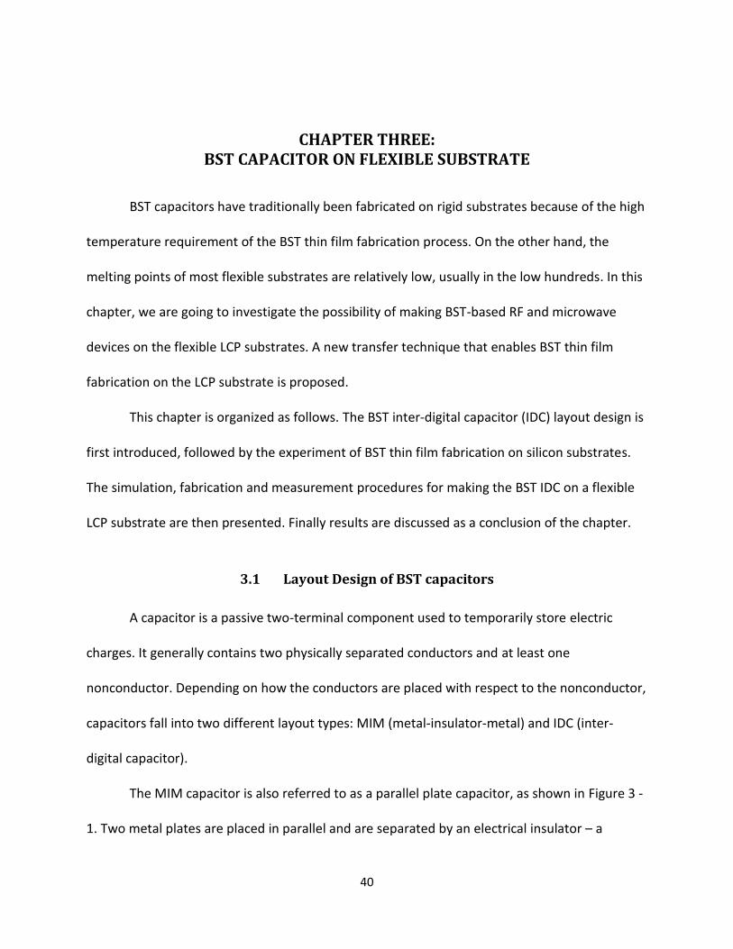
40
CHAPTER THREE: BST CAPACITOR ON FLEXIBLE SUBSTRATE
BST capacitors have traditionally been fabricated on rigid substrates because of the high
temperature requirement of the BST thin film fabrication process. On the other hand, the
melting points of most flexible substrates are relatively low, usually in the low hundreds. In this
chapter, we are going to investigate the possibility of making BST-based RF and microwave
devices on the flexible LCP substrates. A new transfer technique that enables BST thin film
fabrication on the LCP substrate is proposed.
This chapter is organized as follows. The BST inter-digital capacitor (IDC) layout design is
first introduced, followed by the experiment of BST thin film fabrication on silicon substrates.
The simulation, fabrication and measurement procedures for making the BST IDC on a flexible
LCP substrate are then presented. Finally results are discussed as a conclusion of the chapter.
3.1 Layout Design of BST capacitors
A capacitor is a passive two-terminal component used to temporarily store electric
charges. It generally contains two physically separated conductors and at least one
nonconductor. Depending on how the conductors are placed with respect to the nonconductor,
capacitors fall into two different layout types: MIM (metal-insulator-metal) and IDC (inter-
digital capacitor).
The MIM capacitor is also referred to as a parallel plate capacitor, as shown in Figure 3 -
1. Two metal plates are placed in parallel and are separated by an electrical insulator – a
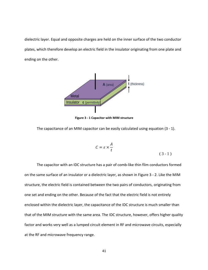
41
dielectric layer. Equal and opposite charges are held on the inner surface of the two conductor
plates, which therefore develop an electric field in the insulator originating from one plate and
ending on the other.
Figure 3 - 1 Capacitor with MIM structure
The capacitance of an MIM capacitor can be easily calculated using equation (3 - 1).
( 3 - 1 )
The capacitor with an IDC structure has a pair of comb-like thin film conductors formed
on the same surface of an insulator or a dielectric layer, as shown in Figure 3 - 2. Like the MIM
structure, the electric field is contained between the two pairs of conductors, originating from
one set and ending on the other. Because of the fact that the electric field is not entirely
enclosed within the dielectric layer, the capacitance of the IDC structure is much smaller than
that of the MIM structure with the same area. The IDC structure, however, offers higher quality
factor and works very well as a lumped circuit element in RF and microwave circuits, especially
at the RF and microwave frequency range.
Insulator
Metal
t (thickness)A (area)
ε (permittivity)
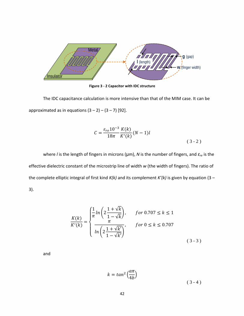
42
Figure 3 - 2 Capacitor with IDC structure
The IDC capacitance calculation is more intensive than that of the MIM case. It can be
approximated as in equations (3 – 2) – (3 – 7) [92].
( 3 - 2 )
where l is the length of fingers in microns (μm), N is the number of fingers, and εre is the
effective dielectric constant of the microstrip line of width w (the width of fingers). The ratio of
the complete elliptic integral of first kind K(k) and its complement K’(k) is given by equation (3 –
3).
( 3 - 3 )
and
( 3 - 4 )
g (gap)
w (finger width)
Insulator
l (length)
Metal
43
( 3 - 5 )
( 3 - 6 )
( 3 - 7 )
where w is the width of fingers and g is the gap size between two adjacent fingers, with
units both in µm.
For BST-based capacitors, the IDC structure is preferred, since it usually requires only
one step lithography process to pattern the electrodes. Moreover, the MIM structure requires
using high quality metal, such as platinum, as the bottom electrode that can resist oxidation
during the high-temperature procedure for BST thin film processing. Nonetheless, the process
for making IDC structure doesn’t limit the type of metal that can be used for the electrodes,
hence copper, which is inexpensive and highly conductive, can be used. The focus this chapter
will be on BST-based IDC structures that will be fabricated on flexible LCP substrates.
3.2 BST Thin Film on a Silicon Substrate
Before talking about the BST thin films on the LCP substrates, we need to first look into
how to make good quality BST thin films on the silicon substrates, since these BST thin films will
then be transferred onto the LCP substrates, as described in Section 2.4.
44
3.2.1 Thermal Incompatibility between BST Thin Film and Silicon Substrate
BST and silicon are not thermally compatible. There is a large difference between the
coefficients of thermal expansion (CTE) of these two materials. CTE is a measure of fractional
change in dimension per degree change in temperature at a fixed pressure. It is usually
expressed in parts-per-million/oC (ppm/oC). The CTE for silicon material is 2.6 ppm/oC, while the
CTE for BST thin film is about 10 ppm/oC [93] [94] at room temperature and atmospheric
pressure.
Right after the RF magnetron sputtering deposition, the BST thin film is mostly
amorphous. High-temperature annealing process of over 700oC is required in order to
crystallize the BST thin film. The big mismatch in CTE between the BST thin film and the silicon
substrate will cause BST film to crack during annealing, as shown in Figure 3 - 3. Depending on
the annealing condition, the extent of cracking varies. Generally, the higher the annealing
temperature and longer the annealing time, the worse the cracking in the BST thin film.
Parameters for both sputtering and annealing processes need to be properly designed in
order to reduce the strain and stress in the BST thin film and the silicon substrate, thereby,
eliminating BST thin film cracking.
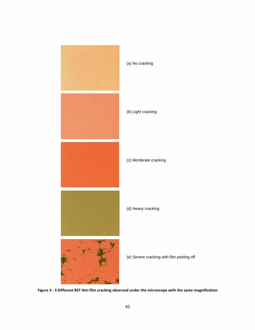
45
Figure 3 - 3 Different BST thin film cracking observed under the microscope with the same magnification
(a) No cracking
(b) Light cracking
(c) Morderate cracking
(d) Heavy cracking
(e) Severe cracking with film peeling off
46
3.2.2 Deposition and Annealing Parameters for BST Thin Film on a Silicon Substrate
During our experiments, it was found that when the substrate temperature is elevated
during the sputtering process, the annealing temperature can also be increased accordingly
without causing cracking in the BST thin film. The parameters used in this work for sputtering
and annealing the BST thin film on the silicon substrate are listed as follows:
RF magnetron sputtering
Substrate temperature: 650 oC
RF power: 200 W
Chamber pressure: 20 mTorr
Ar:O2: 10 sccm : 5 sccm (sccm: standard cubic centimeter per minute)
Oven annealing in atmosphere with O2 flow
Temperature: 700 oC
Duration: 2 hours
3.2.3 Material Characterization of the BST Thin Film on a Silicon Substrate
After the BST thin film was deposited and annealed on the silicon substrate, Rutherford
Backscattering Spectrometry (RBS) and X-ray diffraction (XRD) were performed to inspect the
material composition and crystallization respectively.
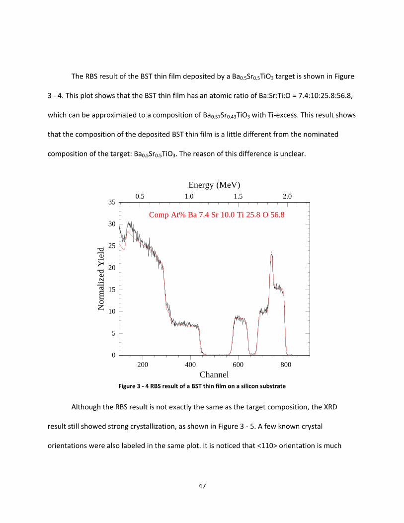
47
The RBS result of the BST thin film deposited by a Ba0.5Sr0.5TiO3 target is shown in Figure
3 - 4. This plot shows that the BST thin film has an atomic ratio of Ba:Sr:Ti:O = 7.4:10:25.8:56.8,
which can be approximated to a composition of Ba0.57Sr0.43TiO3 with Ti-excess. This result shows
that the composition of the deposited BST thin film is a little different from the nominated
composition of the target: Ba0.5Sr0.5TiO3. The reason of this difference is unclear.
Figure 3 - 4 RBS result of a BST thin film on a silicon substrate
Although the RBS result is not exactly the same as the target composition, the XRD
result still showed strong crystallization, as shown in Figure 3 - 5. A few known crystal
orientations were also labeled in the same plot. It is noticed that <110> orientation is much
200 400 600 800
Channel
0
5
10
15
20
25
30
35
No
rmal
ized
Yie
ld
0.5 1.0 1.5 2.0
Energy (MeV)
Comp At% Ba 7.4 Sr 10.0 Ti 25.8 O 56.8
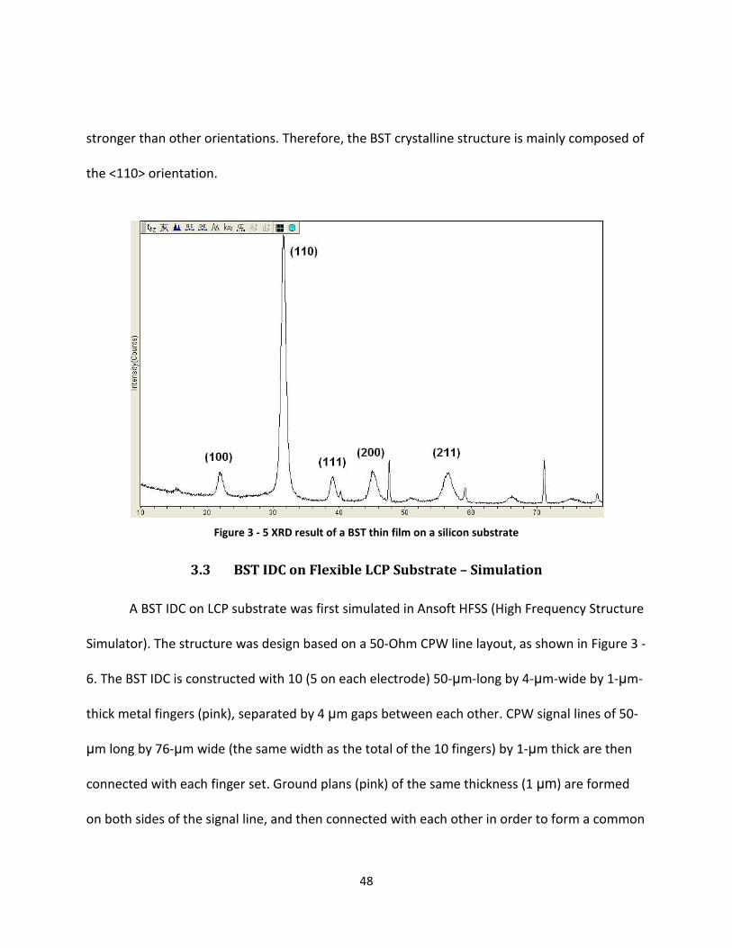
48
stronger than other orientations. Therefore, the BST crystalline structure is mainly composed of
the <110> orientation.
Figure 3 - 5 XRD result of a BST thin film on a silicon substrate
3.3 BST IDC on Flexible LCP Substrate – Simulation
A BST IDC on LCP substrate was first simulated in Ansoft HFSS (High Frequency Structure
Simulator). The structure was design based on a 50-Ohm CPW line layout, as shown in Figure 3 -
6. The BST IDC is constructed with 10 (5 on each electrode) 50-μm-long by 4-μm-wide by 1-μm-
thick metal fingers (pink), separated by 4 μm gaps between each other. CPW signal lines of 50-
μm long by 76-μm wide (the same width as the total of the 10 fingers) by 1-μm thick are then
connected with each finger set. Ground plans (pink) of the same thickness (1 μm) are formed
on both sides of the signal line, and then connected with each other in order to form a common
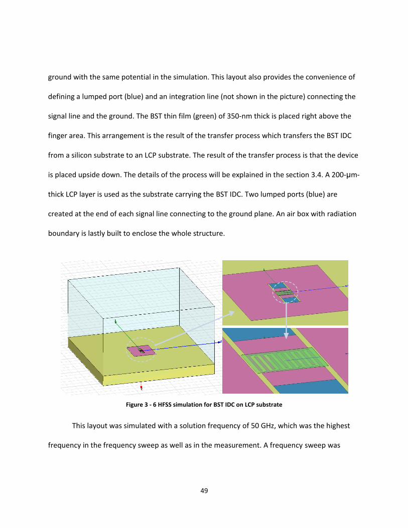
49
ground with the same potential in the simulation. This layout also provides the convenience of
defining a lumped port (blue) and an integration line (not shown in the picture) connecting the
signal line and the ground. The BST thin film (green) of 350-nm thick is placed right above the
finger area. This arrangement is the result of the transfer process which transfers the BST IDC
from a silicon substrate to an LCP substrate. The result of the transfer process is that the device
is placed upside down. The details of the process will be explained in the section 3.4. A 200-μm-
thick LCP layer is used as the substrate carrying the BST IDC. Two lumped ports (blue) are
created at the end of each signal line connecting to the ground plane. An air box with radiation
boundary is lastly built to enclose the whole structure.
Figure 3 - 6 HFSS simulation for BST IDC on LCP substrate
This layout was simulated with a solution frequency of 50 GHz, which was the highest
frequency in the frequency sweep as well as in the measurement. A frequency sweep was
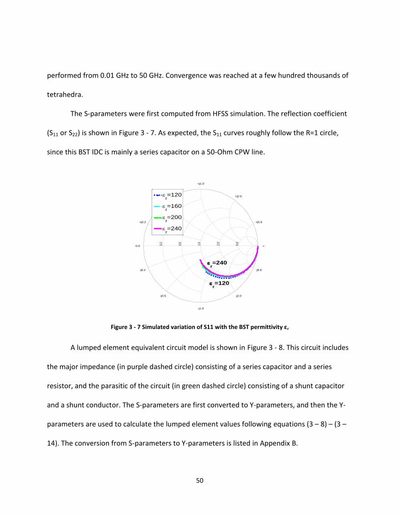
50
performed from 0.01 GHz to 50 GHz. Convergence was reached at a few hundred thousands of
tetrahedra.
The S-parameters were first computed from HFSS simulation. The reflection coefficient
(S11 or S22) is shown in Figure 3 - 7. As expected, the S11 curves roughly follow the R=1 circle,
since this BST IDC is mainly a series capacitor on a 50-Ohm CPW line.
Figure 3 - 7 Simulated variation of S11 with the BST permittivity εr
A lumped element equivalent circuit model is shown in Figure 3 - 8. This circuit includes
the major impedance (in purple dashed circle) consisting of a series capacitor and a series
resistor, and the parasitic of the circuit (in green dashed circle) consisting of a shunt capacitor
and a shunt conductor. The S-parameters are first converted to Y-parameters, and then the Y-
parameters are used to calculate the lumped element values following equations (3 – 8) – (3 –
14). The conversion from S-parameters to Y-parameters is listed in Appendix B.
0.2
0.5
1.0
2.0
5.0
+j0.2
-j0.2
+j0.5
-j0.5
+j1.0
-j1.0
+j2.0
-j2.0
+j5.0
-j5.0
0.0
r=120
r=160
r=200
r=240
r=240
r=120
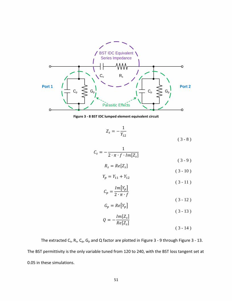
51
Figure 3 - 8 BST IDC lumped element equivalent circuit
( 3 - 8 )
( 3 - 9 )
( 3 - 10 )
( 3 - 11 )
( 3 - 12 )
( 3 - 13 )
( 3 - 14 )
The extracted Cs, Rs, Cp, Gp and Q factor are plotted in Figure 3 - 9 through Figure 3 - 13.
The BST permittivity is the only variable tuned from 120 to 240, with the BST loss tangent set at
0.05 in these simulations.
Cs Rs
Cp Gp Cp Gp
Port 1 Port 2
BST IDC Equivalent
Series Impedance
Parasitic Effects
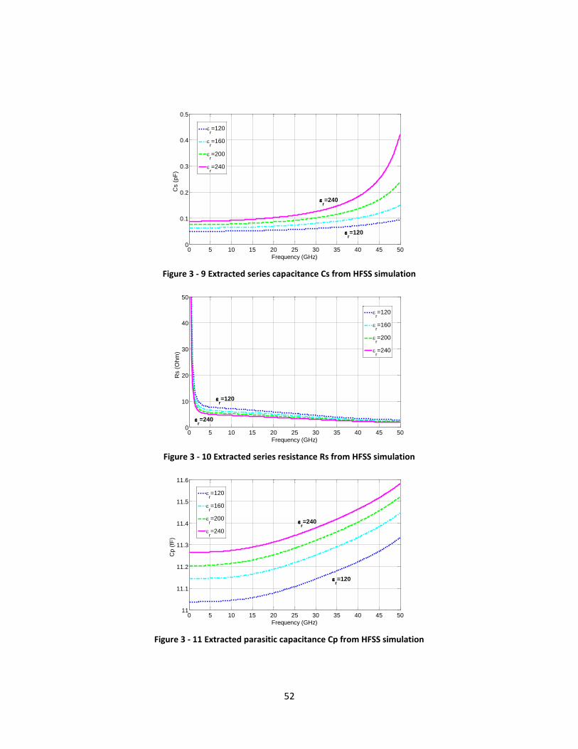
52
Figure 3 - 9 Extracted series capacitance Cs from HFSS simulation
Figure 3 - 10 Extracted series resistance Rs from HFSS simulation
Figure 3 - 11 Extracted parasitic capacitance Cp from HFSS simulation
0 5 10 15 20 25 30 35 40 45 500
0.1
0.2
0.3
0.4
0.5
Frequency (GHz)
Cs (
pF
)
r=120
r=160
r=200
r=240
r=120
r=240
0 5 10 15 20 25 30 35 40 45 500
10
20
30
40
50
Frequency (GHz)
Rs (
Oh
m)
r=120
r=160
r=200
r=240
r=240
r=120
0 5 10 15 20 25 30 35 40 45 5011
11.1
11.2
11.3
11.4
11.5
11.6
Frequency (GHz)
Cp
(fF
)
r=120
r=160
r=200
r=240
r=240
r=120
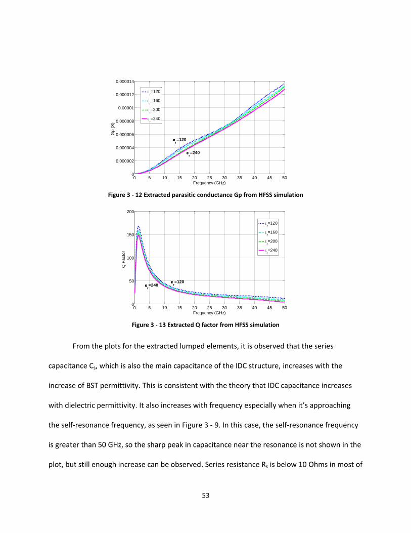
53
Figure 3 - 12 Extracted parasitic conductance Gp from HFSS simulation
Figure 3 - 13 Extracted Q factor from HFSS simulation
From the plots for the extracted lumped elements, it is observed that the series
capacitance Cs, which is also the main capacitance of the IDC structure, increases with the
increase of BST permittivity. This is consistent with the theory that IDC capacitance increases
with dielectric permittivity. It also increases with frequency especially when it’s approaching
the self-resonance frequency, as seen in Figure 3 - 9. In this case, the self-resonance frequency
is greater than 50 GHz, so the sharp peak in capacitance near the resonance is not shown in the
plot, but still enough increase can be observed. Series resistance Rs is below 10 Ohms in most of
0 5 10 15 20 25 30 35 40 45 500
0.000002
0.000004
0.000006
0.000008
0.00001
0.000012
0.000014
Frequency (GHz)
Gp
(S
)
r=120
r=160
r=200
r=240
r=120
r=240
0 5 10 15 20 25 30 35 40 45 500
50
100
150
200
Frequency (GHz)
Q F
acto
r
r=120
r=160
r=200
r=240
r=240
r=120
54
the simulated frequencies and it decreases with frequency. Also, higher permittivity provides
lower Rs, as shown in Figure 3 - 10. Parasitic capacitance Cp is about one magnitude smaller
than that of the main capacitance Cs, as shown in Figure 3 - 11. Parasitic conductance is in the
10-5 range, which is fairly small, as shown in Figure 3 - 12. Q factor curves of different BST
permittivity are very similar in readings, and they generally decrease with frequency after the
peak at around 1 GHz. It is also observed that higher permittivity leads to slightly lower Q, as
shown in Figure 3 - 13.
3.4 BST IDC on Flexible LCP Substrate – Fabrication and Transfer
The fabrication of BST IDC on LCP started with using a rigid silicon wafer as a sacrificial
substrate. Test grade N-type single-side-polished (SSP) silicon wafers with <100> crystalline
orientation were chosen for their quality, ease of processing and price considerations. After the
silicon wafers were cleaned using acetone-methanol-deionized water (DI water), a 700-nm-
thick SiO2 layer was first grown on the silicon wafer in a wet oxidation oven at 1100 oC. This
layer was mainly served as a protection for the BST thin film and the LCP substrate during the
silicon etching process. There are a few reasons that the SiO2 thin film was chosen in this
process. First, it is very easy to grow SiO2 on bare silicon wafers. Second, both the BST thin film
and the LCP substrate do not resist KOH solution, while the etching rate for SiO2 in KOH
solution is at least two magnitudes slower than that for silicon. Therefore, SiO2 layer can be
used as the etching stopper / protection for both the BST and the LCP. Third, SiO2 is
transparent. After the BST IDCs are transferred onto the LCP substrate, measurement windows
55
need to be opened in order to expose the CPW lines for the CPW probe contact. Transparent
SiO2 layer makes it easier for alignment as for where to open the measurement windows. Last
but not the least, SiO2 can be etched easily in a buffered oxide etch (BOE) solution.
After the SiO2 was thermally grown on the silicon wafer, BST thin film of 350 nm was
deposited on this SiO2/Si substrate using RF magnetron sputtering with a substrate
temperature of 650 oC, as mentioned in section 3.2.2. Shipley 1813, a positive photoresist (PR),
was then used in the photolithographic process to create a mask for BST thin film wet etching.
The spin rate was set to 3000 revolutions per minute (rpm), which gave a PR thickness of about
1.3 µm. This thickness is enough for most etching processes. A commercially available HF
solution diluted to 2% was used to etch the BST thin film. The BST etching process is not
straightforward, for the BST thin film is transparent and it is difficult to tell if etching is finished
or not. Since the BST thin film presents the same effect as the SiO2 thin film (color chart) that
the interference of light reflected by the surface of the BST thin film and that reflected by the
thin film or substrate right underneath the BST thin film gives a certain color to the film when
the BST thin film is of a certain thickness. Therefore, during the etching process, when the
thickness of the BST thin film kept reducing, the color seen at a certain angle changed
accordingly. From our experience, a proper rate of color changing implies a good rate of
etching. When it comes close to the end of the etching process, the color of the BST thin film
appears very dark mixed with navy and a tiny bit of red, which is not observed when the film is
relatively thick. When this color is observed, it means the wafer is ready to be taken out of the
etchant soon. It is also very important that the BST thin film is etched before annealing, since
56
the BST thin film will become very resistant to the etchant after the high temperature annealing
process, during which the BST thin film is crystallized to some extent. Although HF solution with
higher concentration, for example 10% and above, can be used to etch such films, it tends to
peel off PR as well. This makes it impossible to obtain well-defined BST patterns after etching.
After the BST thin film etching was finished, the PR on the wafer was cleaned up before
the wafer was sent to be annealed. This clean-up process included the acetone-methanol-DI
water rinse, followed by a plasma asher process to clean up any PR residuals if any. The BST
thin film annealing took place in a programmable box oven. The temperature was set to 700 oC
for 2 hours, with a ramp-up rate of 10o/min. The chamber stayed at atmosphere pressure at all
times and an oxygen flow was provided during this process.
After annealing, another layer of Shipley 1813 PR was spun and patterned, preparing for
the metal lift-off process. In this process, the spin rate was set to 1000 rpm, which gave a PR
thickness of about 2 µm. This thickness was the least requirement for lifting-off metal fingers
and CPW line patterns of 1 µm. After the PR was exposed by a mask aligner, it needed to go
through some special treatment in order to create a side wall profile that was vertical or with
an overhang. This is extremely important for our lift-off process because of the small features in
the design: 4-µm-wide finger patterns separated by the 4-µm-wide gaps. The wafer with the
exposed PR was soaked in chlorobenzene solution for 16 minutes. The purpose of this step was
to harden the top layer of the PR to make it harder to develop away. When the wafer was being
developed in CD-26 developer, the layer which was not hardened tend to be developed faster
than the layer that was, which created an overhanging or under-cutting effect if seen from the
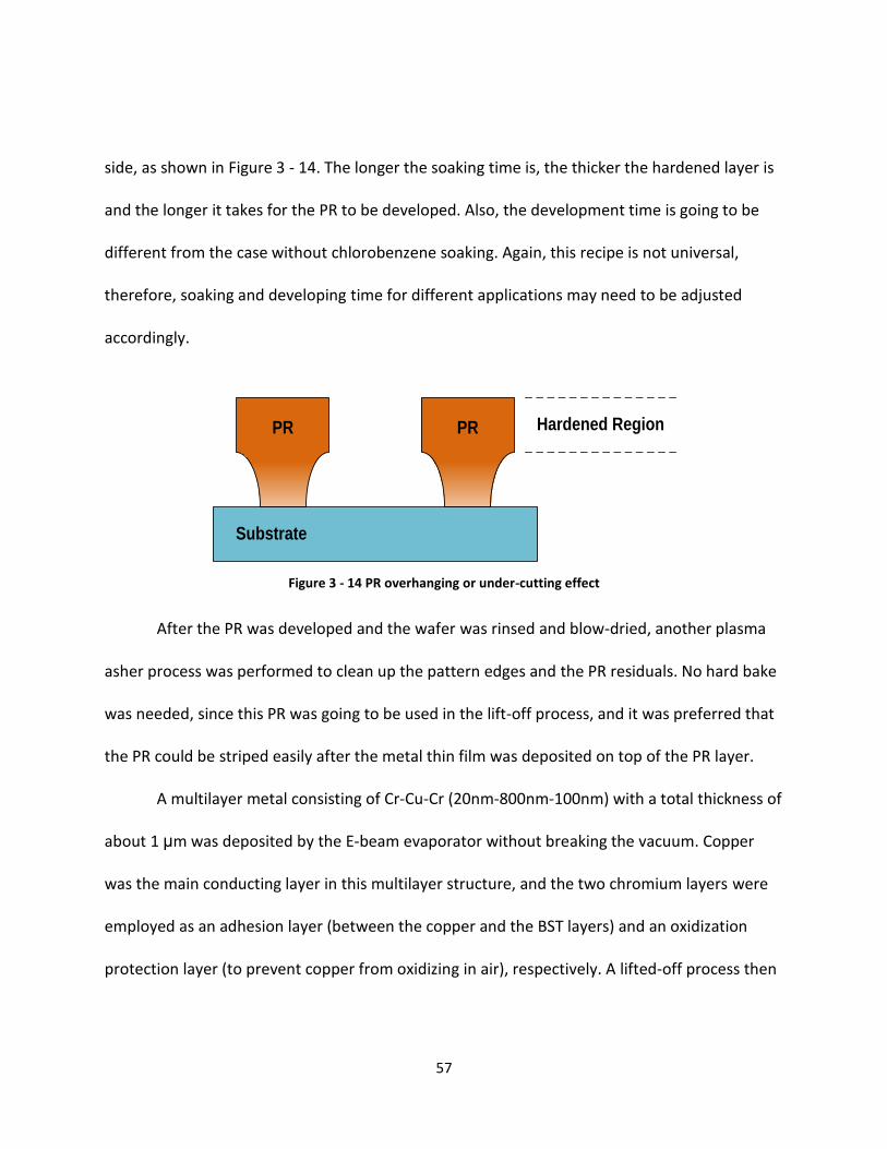
57
side, as shown in Figure 3 - 14. The longer the soaking time is, the thicker the hardened layer is
and the longer it takes for the PR to be developed. Also, the development time is going to be
different from the case without chlorobenzene soaking. Again, this recipe is not universal,
therefore, soaking and developing time for different applications may need to be adjusted
accordingly.
Figure 3 - 14 PR overhanging or under-cutting effect
After the PR was developed and the wafer was rinsed and blow-dried, another plasma
asher process was performed to clean up the pattern edges and the PR residuals. No hard bake
was needed, since this PR was going to be used in the lift-off process, and it was preferred that
the PR could be striped easily after the metal thin film was deposited on top of the PR layer.
A multilayer metal consisting of Cr-Cu-Cr (20nm-800nm-100nm) with a total thickness of
about 1 μm was deposited by the E-beam evaporator without breaking the vacuum. Copper
was the main conducting layer in this multilayer structure, and the two chromium layers were
employed as an adhesion layer (between the copper and the BST layers) and an oxidization
protection layer (to prevent copper from oxidizing in air), respectively. A lifted-off process then
Substrate
PR PR Hardened Region
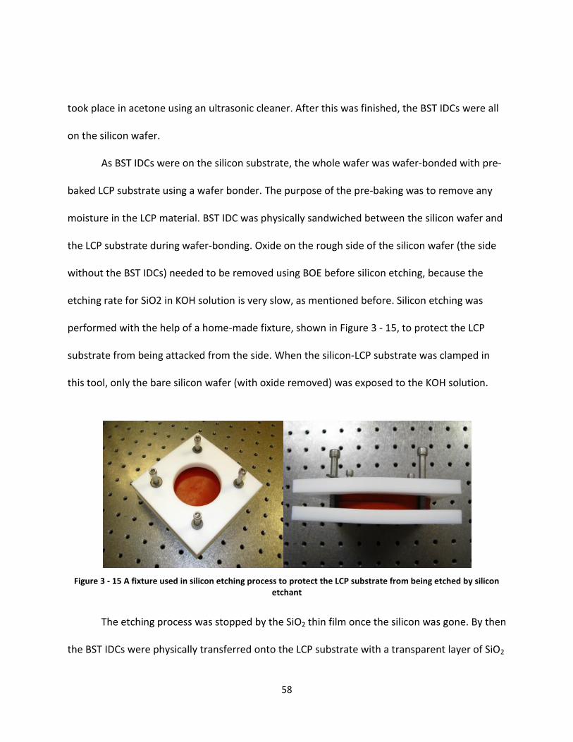
58
took place in acetone using an ultrasonic cleaner. After this was finished, the BST IDCs were all
on the silicon wafer.
As BST IDCs were on the silicon substrate, the whole wafer was wafer-bonded with pre-
baked LCP substrate using a wafer bonder. The purpose of the pre-baking was to remove any
moisture in the LCP material. BST IDC was physically sandwiched between the silicon wafer and
the LCP substrate during wafer-bonding. Oxide on the rough side of the silicon wafer (the side
without the BST IDCs) needed to be removed using BOE before silicon etching, because the
etching rate for SiO2 in KOH solution is very slow, as mentioned before. Silicon etching was
performed with the help of a home-made fixture, shown in Figure 3 - 15, to protect the LCP
substrate from being attacked from the side. When the silicon-LCP substrate was clamped in
this tool, only the bare silicon wafer (with oxide removed) was exposed to the KOH solution.
Figure 3 - 15 A fixture used in silicon etching process to protect the LCP substrate from being etched by silicon etchant
The etching process was stopped by the SiO2 thin film once the silicon was gone. By then
the BST IDCs were physically transferred onto the LCP substrate with a transparent layer of SiO2
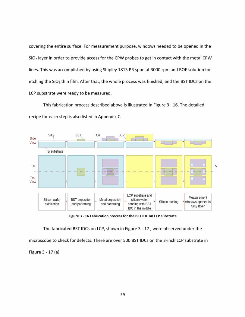
59
covering the entire surface. For measurement purpose, windows needed to be opened in the
SiO2 layer in order to provide access for the CPW probes to get in contact with the metal CPW
lines. This was accomplished by using Shipley 1813 PR spun at 3000 rpm and BOE solution for
etching the SiO2 thin film. After that, the whole process was finished, and the BST IDCs on the
LCP substrate were ready to be measured.
This fabrication process described above is illustrated in Figure 3 - 16. The detailed
recipe for each step is also listed in Appendix C.
Figure 3 - 16 Fabrication process for the BST IDC on LCP substrate
The fabricated BST IDCs on LCP, shown in Figure 3 - 17 , were observed under the
microscope to check for defects. There are over 500 BST IDCs on the 3-inch LCP substrate in
Figure 3 - 17 (a).
Side
View
Top
View
Silicon wafer
oxidization
BST deposition
and patterning
Metal deposition
and patterning
LCP substrate and
silicon wafer
bonding with BST
IDC in the middle
Silicon etching
Measurement
windows opened in
SiO2 layer
Si substrate
SiO2 BST Cu LCP
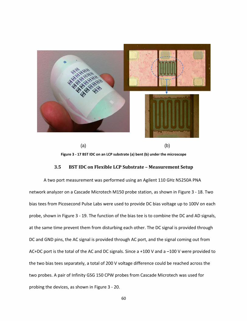
60
Figure 3 - 17 BST IDC on an LCP substrate (a) bent (b) under the microscope
3.5 BST IDC on Flexible LCP Substrate – Measurement Setup
A two port measurement was performed using an Agilent 110 GHz N5250A PNA
network analyzer on a Cascade Microtech M150 probe station, as shown in Figure 3 - 18. Two
bias tees from Picosecond Pulse Labs were used to provide DC bias voltage up to 100V on each
probe, shown in Figure 3 - 19. The function of the bias tee is to combine the DC and AD signals,
at the same time prevent them from disturbing each other. The DC signal is provided through
DC and GND pins, the AC signal is provided through AC port, and the signal coming out from
AC+DC port is the total of the AC and DC signals. Since a +100 V and a –100 V were provided to
the two bias tees separately, a total of 200 V voltage difference could be reached across the
two probes. A pair of Infinity GSG 150 CPW probes from Cascade Microtech was used for
probing the devices, as shown in Figure 3 - 20.
(a) (b)
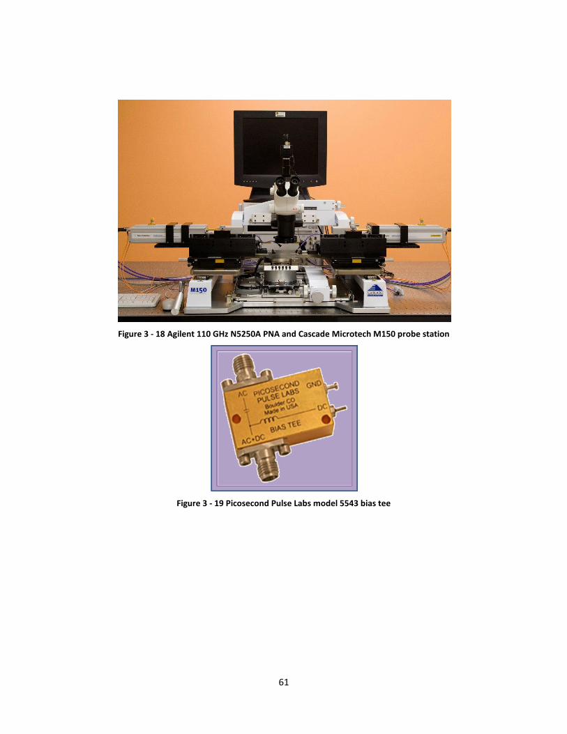
61
Figure 3 - 18 Agilent 110 GHz N5250A PNA and Cascade Microtech M150 probe station
Figure 3 - 19 Picosecond Pulse Labs model 5543 bias tee
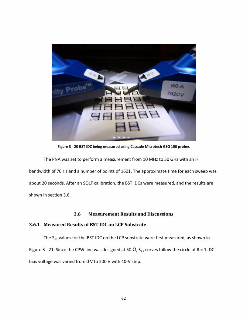
62
Figure 3 - 20 BST IDC being measured using Cascade Microtech GSG 150 probes
The PNA was set to perform a measurement from 10 MHz to 50 GHz with an IF
bandwidth of 70 Hz and a number of points of 1601. The approximate time for each sweep was
about 20 seconds. After an SOLT calibration, the BST IDCs were measured, and the results are
shown in section 3.6.
3.6 Measurement Results and Discussions
3.6.1 Measured Results of BST IDC on LCP Substrate
The S11 values for the BST IDC on the LCP substrate were first measured, as shown in
Figure 3 - 21. Since the CPW line was designed at 50 Ω, S11 curves follow the circle of R = 1. DC
bias voltage was varied from 0 V to 200 V with 40-V step.
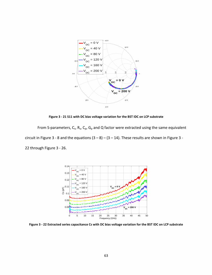
63
Figure 3 - 21 S11 with DC bias voltage variation for the BST IDC on LCP substrate
From S-parameters, Cs, Rs, Cp, Gp and Q factor were extracted using the same equivalent
circuit in Figure 3 - 8 and the equations (3 – 8) – (3 – 14). These results are shown in Figure 3 -
22 through Figure 3 - 26.
Figure 3 - 22 Extracted series capacitance Cs with DC bias voltage variation for the BST IDC on LCP substrate
0.2
0.5
1.0
2.0
5.0
+j0.2
-j0.2
+j0.5
-j0.5
+j1.0
-j1.0
+j2.0
-j2.0
+j5.0
-j5.0
0.0
VDC
= 0 V
VDC
= 40 V
VDC
= 80 V
VDC
= 120 V
VDC
= 160 V
VDC
= 200 V
VDC
= 0 V
VDC
= 200 V
0 5 10 15 20 25 30 35 40 45 50
0.08
0.09
0.1
0.11
0.12
0.13
0.14
Frequency (GHz)
Cs (
pF
)
VDC
= 0 V
VDC
= 40 V
VDC
= 80 V
VDC
= 120 V
VDC
= 160 V
VDC
= 200 V
VDC
= 0 V
VDC
= 200 V
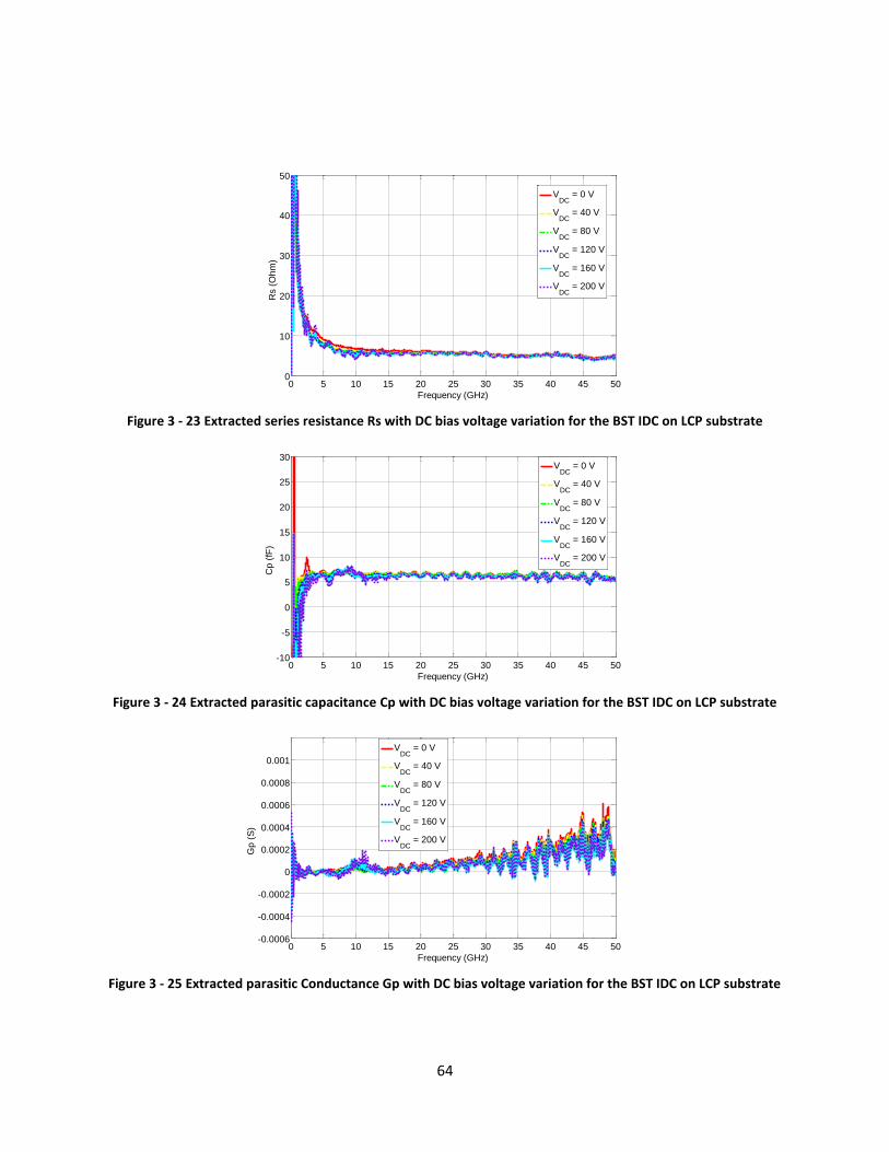
64
Figure 3 - 23 Extracted series resistance Rs with DC bias voltage variation for the BST IDC on LCP substrate
Figure 3 - 24 Extracted parasitic capacitance Cp with DC bias voltage variation for the BST IDC on LCP substrate
Figure 3 - 25 Extracted parasitic Conductance Gp with DC bias voltage variation for the BST IDC on LCP substrate
0 5 10 15 20 25 30 35 40 45 500
10
20
30
40
50
Frequency (GHz)
Rs (
Oh
m)
VDC
= 0 V
VDC
= 40 V
VDC
= 80 V
VDC
= 120 V
VDC
= 160 V
VDC
= 200 V
0 5 10 15 20 25 30 35 40 45 50-10
-5
0
5
10
15
20
25
30
Frequency (GHz)
Cp
(fF
)
VDC
= 0 V
VDC
= 40 V
VDC
= 80 V
VDC
= 120 V
VDC
= 160 V
VDC
= 200 V
0 5 10 15 20 25 30 35 40 45 50-0.0006
-0.0004
-0.0002
0
0.0002
0.0004
0.0006
0.0008
0.001
Frequency (GHz)
Gp
(S
)
VDC
= 0 V
VDC
= 40 V
VDC
= 80 V
VDC
= 120 V
VDC
= 160 V
VDC
= 200 V
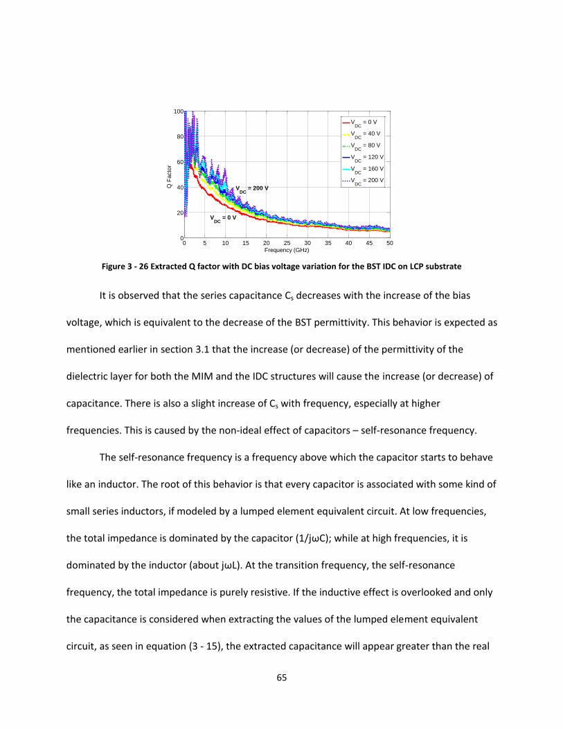
65
Figure 3 - 26 Extracted Q factor with DC bias voltage variation for the BST IDC on LCP substrate
It is observed that the series capacitance Cs decreases with the increase of the bias
voltage, which is equivalent to the decrease of the BST permittivity. This behavior is expected as
mentioned earlier in section 3.1 that the increase (or decrease) of the permittivity of the
dielectric layer for both the MIM and the IDC structures will cause the increase (or decrease) of
capacitance. There is also a slight increase of Cs with frequency, especially at higher
frequencies. This is caused by the non-ideal effect of capacitors – self-resonance frequency.
The self-resonance frequency is a frequency above which the capacitor starts to behave
like an inductor. The root of this behavior is that every capacitor is associated with some kind of
small series inductors, if modeled by a lumped element equivalent circuit. At low frequencies,
the total impedance is dominated by the capacitor (1/jωC); while at high frequencies, it is
dominated by the inductor (about jωL). At the transition frequency, the self-resonance
frequency, the total impedance is purely resistive. If the inductive effect is overlooked and only
the capacitance is considered when extracting the values of the lumped element equivalent
circuit, as seen in equation (3 - 15), the extracted capacitance will appear greater than the real
0 5 10 15 20 25 30 35 40 45 500
20
40
60
80
100
Frequency (GHz)
Q F
acto
r
VDC
= 0 V
VDC
= 40 V
VDC
= 80 V
VDC
= 120 V
VDC
= 160 V
VDC
= 200 V
VDC
= 0 V
VDC
= 200 V
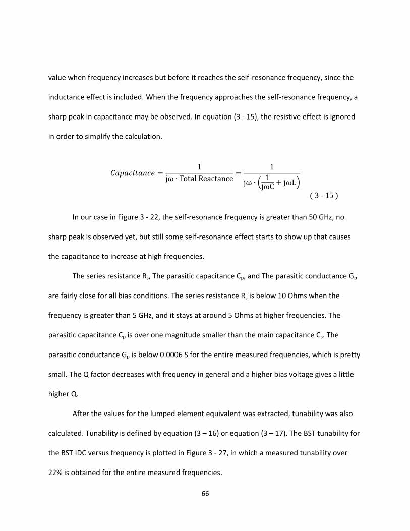
66
value when frequency increases but before it reaches the self-resonance frequency, since the
inductance effect is included. When the frequency approaches the self-resonance frequency, a
sharp peak in capacitance may be observed. In equation (3 - 15), the resistive effect is ignored
in order to simplify the calculation.
( 3 - 15 )
In our case in Figure 3 - 22, the self-resonance frequency is greater than 50 GHz, no
sharp peak is observed yet, but still some self-resonance effect starts to show up that causes
the capacitance to increase at high frequencies.
The series resistance Rs, The parasitic capacitance Cp, and The parasitic conductance Gp
are fairly close for all bias conditions. The series resistance Rs is below 10 Ohms when the
frequency is greater than 5 GHz, and it stays at around 5 Ohms at higher frequencies. The
parasitic capacitance Cp is over one magnitude smaller than the main capacitance Cs. The
parasitic conductance Gp is below 0.0006 S for the entire measured frequencies, which is pretty
small. The Q factor decreases with frequency in general and a higher bias voltage gives a little
higher Q.
After the values for the lumped element equivalent was extracted, tunability was also
calculated. Tunability is defined by equation (3 – 16) or equation (3 – 17). The BST tunability for
the BST IDC versus frequency is plotted in Figure 3 - 27, in which a measured tunability over
22% is obtained for the entire measured frequencies.
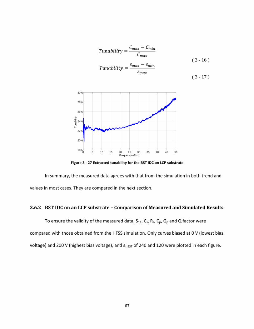
67
( 3 - 16 )
( 3 - 17 )
Figure 3 - 27 Extracted tunability for the BST IDC on LCP substrate
In summary, the measured data agrees with that from the simulation in both trend and
values in most cases. They are compared in the next section.
3.6.2 BST IDC on an LCP substrate – Comparison of Measured and Simulated Results
To ensure the validity of the measured data, S11, Cs, Rs, Cp, Gp and Q factor were
compared with those obtained from the HFSS simulation. Only curves biased at 0 V (lowest bias
voltage) and 200 V (highest bias voltage), and εr,BST of 240 and 120 were plotted in each figure.
0 5 10 15 20 25 30 35 40 45 5018%
20%
22%
24%
26%
28%
30%
Frequency (GHz)
Tu
na
bili
ty
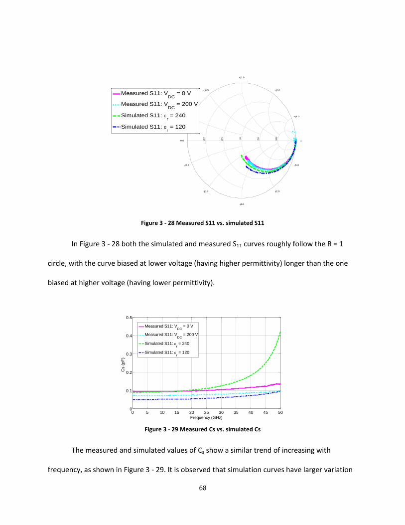
68
Figure 3 - 28 Measured S11 vs. simulated S11
In Figure 3 - 28 both the simulated and measured S11 curves roughly follow the R = 1
circle, with the curve biased at lower voltage (having higher permittivity) longer than the one
biased at higher voltage (having lower permittivity).
Figure 3 - 29 Measured Cs vs. simulated Cs
The measured and simulated values of Cs show a similar trend of increasing with
frequency, as shown in Figure 3 - 29. It is observed that simulation curves have larger variation
0.2
0.5
1.0
2.0
5.0
+j0.2
-j0.2
+j0.5
-j0.5
+j1.0
-j1.0
+j2.0
-j2.0
+j5.0
-j5.0
0.0
Measured S11: VDC
= 0 V
Measured S11: VDC
= 200 V
Simulated S11: r = 240
Simulated S11: r = 120
0 5 10 15 20 25 30 35 40 45 500
0.1
0.2
0.3
0.4
0.5
Frequency (GHz)
Cs (
pF
)
Measured S11: VDC
= 0 V
Measured S11: VDC
= 200 V
Simulated S11: r = 240
Simulated S11: r = 120
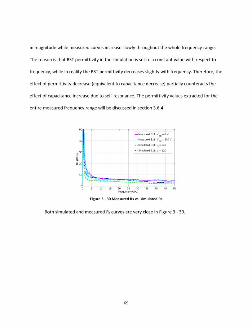
69
in magnitude while measured curves increase slowly throughout the whole frequency range.
The reason is that BST permittivity in the simulation is set to a constant value with respect to
frequency, while in reality the BST permittivity decreases slightly with frequency. Therefore, the
effect of permittivity decrease (equivalent to capacitance decrease) partially counteracts the
effect of capacitance increase due to self-resonance. The permittivity values extracted for the
entire measured frequency range will be discussed in section 3.6.4.
Figure 3 - 30 Measured Rs vs. simulated Rs
Both simulated and measured Rs curves are very close in Figure 3 - 30.
0 5 10 15 20 25 30 35 40 45 500
10
20
30
40
50
Frequency (GHz)
Rs (
Oh
m)
Measured S11: VDC
= 0 V
Measured S11: VDC
= 200 V
Simulated S11: r = 240
Simulated S11: r = 120
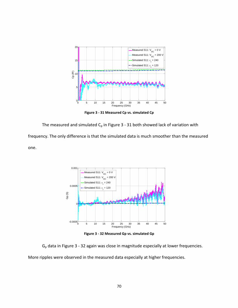
70
Figure 3 - 31 Measured Cp vs. simulated Cp
The measured and simulated Cp in Figure 3 - 31 both showed lack of variation with
frequency. The only difference is that the simulated data is much smoother than the measured
one.
Figure 3 - 32 Measured Gp vs. simulated Gp
Gp data in Figure 3 - 32 again was close in magnitude especially at lower frequencies.
More ripples were observed in the measured data especially at higher frequencies.
0 5 10 15 20 25 30 35 40 45 500
5
10
15
20
Frequency (GHz)
Cp
(fF
)
Measured S11: VDC
= 0 V
Measured S11: VDC
= 200 V
Simulated S11: r = 240
Simulated S11: r = 120
0 5 10 15 20 25 30 35 40 45 50-0.0005
0
0.0005
0.001
Frequency (GHz)
Gp
(S
)
Measured S11: VDC
= 0 V
Measured S11: VDC
= 200 V
Simulated S11: r = 240
Simulated S11: r = 120
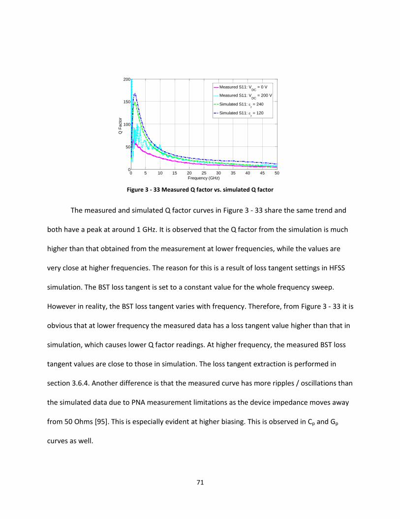
71
Figure 3 - 33 Measured Q factor vs. simulated Q factor
The measured and simulated Q factor curves in Figure 3 - 33 share the same trend and
both have a peak at around 1 GHz. It is observed that the Q factor from the simulation is much
higher than that obtained from the measurement at lower frequencies, while the values are
very close at higher frequencies. The reason for this is a result of loss tangent settings in HFSS
simulation. The BST loss tangent is set to a constant value for the whole frequency sweep.
However in reality, the BST loss tangent varies with frequency. Therefore, from Figure 3 - 33 it is
obvious that at lower frequency the measured data has a loss tangent value higher than that in
simulation, which causes lower Q factor readings. At higher frequency, the measured BST loss
tangent values are close to those in simulation. The loss tangent extraction is performed in
section 3.6.4. Another difference is that the measured curve has more ripples / oscillations than
the simulated data due to PNA measurement limitations as the device impedance moves away
from 50 Ohms [95]. This is especially evident at higher biasing. This is observed in Cp and Gp
curves as well.
0 5 10 15 20 25 30 35 40 45 500
50
100
150
200
Frequency (GHz)
Q F
acto
r
Measured S11: VDC
= 0 V
Measured S11: VDC
= 200 V
Simulated S11: r = 240
Simulated S11: r = 120
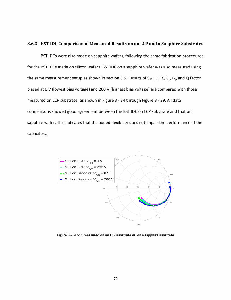
72
3.6.3 BST IDC Comparison of Measured Results on an LCP and a Sapphire Substrates
BST IDCs were also made on sapphire wafers, following the same fabrication procedures
for the BST IDCs made on silicon wafers. BST IDC on a sapphire wafer was also measured using
the same measurement setup as shown in section 3.5. Results of S11, Cs, Rs, Cp, Gp and Q factor
biased at 0 V (lowest bias voltage) and 200 V (highest bias voltage) are compared with those
measured on LCP substrate, as shown in Figure 3 - 34 through Figure 3 - 39. All data
comparisons showed good agreement between the BST IDC on LCP substrate and that on
sapphire wafer. This indicates that the added flexibility does not impair the performance of the
capacitors.
Figure 3 - 34 S11 measured on an LCP substrate vs. on a sapphire substrate
0.2
0.5
1.0
2.0
5.0
+j0.2
-j0.2
+j0.5
-j0.5
+j1.0
-j1.0
+j2.0
-j2.0
+j5.0
-j5.0
0.0
S11 on LCP: VDC
= 0 V
S11 on LCP: VDC
= 200 V
S11 on Sapphire: VDC
= 0 V
S11 on Sapphire: VDC
= 200 V
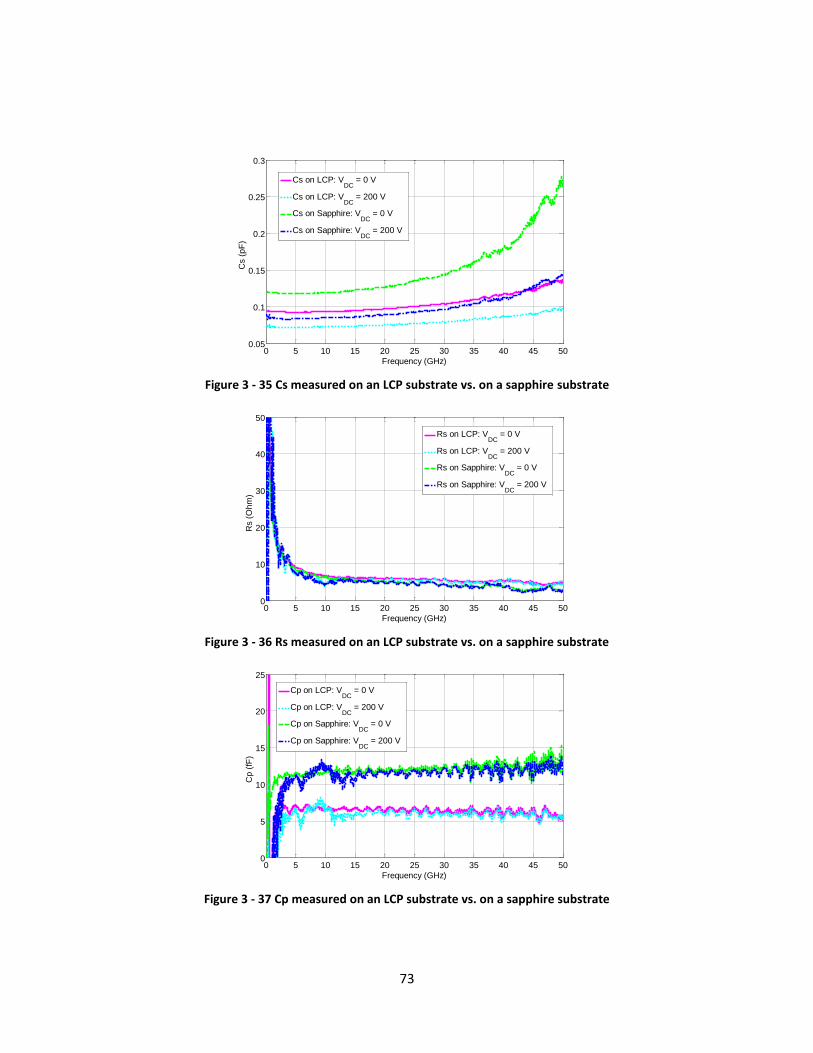
73
Figure 3 - 35 Cs measured on an LCP substrate vs. on a sapphire substrate
Figure 3 - 36 Rs measured on an LCP substrate vs. on a sapphire substrate
Figure 3 - 37 Cp measured on an LCP substrate vs. on a sapphire substrate
0 5 10 15 20 25 30 35 40 45 500.05
0.1
0.15
0.2
0.25
0.3
Frequency (GHz)
Cs (
pF
)
Cs on LCP: VDC
= 0 V
Cs on LCP: VDC
= 200 V
Cs on Sapphire: VDC
= 0 V
Cs on Sapphire: VDC
= 200 V
0 5 10 15 20 25 30 35 40 45 500
10
20
30
40
50
Frequency (GHz)
Rs (
Oh
m)
Rs on LCP: VDC
= 0 V
Rs on LCP: VDC
= 200 V
Rs on Sapphire: VDC
= 0 V
Rs on Sapphire: VDC
= 200 V
0 5 10 15 20 25 30 35 40 45 500
5
10
15
20
25
Frequency (GHz)
Cp
(fF
)
Cp on LCP: VDC
= 0 V
Cp on LCP: VDC
= 200 V
Cp on Sapphire: VDC
= 0 V
Cp on Sapphire: VDC
= 200 V
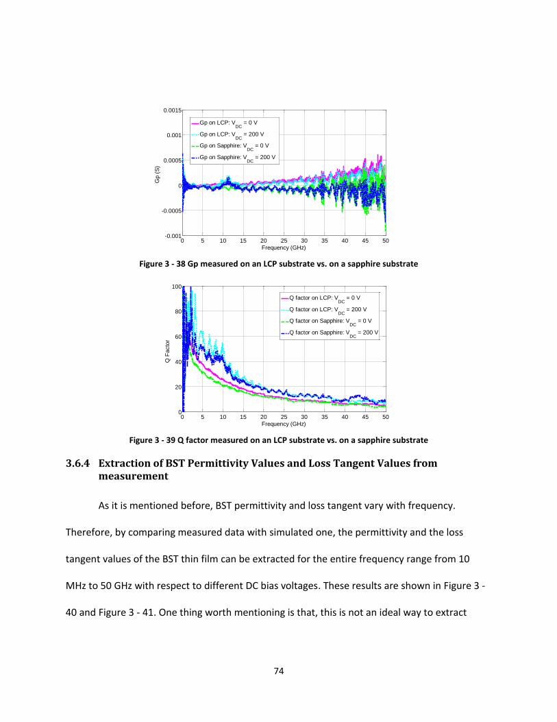
74
Figure 3 - 38 Gp measured on an LCP substrate vs. on a sapphire substrate
Figure 3 - 39 Q factor measured on an LCP substrate vs. on a sapphire substrate
3.6.4 Extraction of BST Permittivity Values and Loss Tangent Values from measurement
As it is mentioned before, BST permittivity and loss tangent vary with frequency.
Therefore, by comparing measured data with simulated one, the permittivity and the loss
tangent values of the BST thin film can be extracted for the entire frequency range from 10
MHz to 50 GHz with respect to different DC bias voltages. These results are shown in Figure 3 -
40 and Figure 3 - 41. One thing worth mentioning is that, this is not an ideal way to extract
0 5 10 15 20 25 30 35 40 45 50-0.001
-0.0005
0
0.0005
0.001
0.0015
Frequency (GHz)
Gp
(S
)
Gp on LCP: VDC
= 0 V
Gp on LCP: VDC
= 200 V
Gp on Sapphire: VDC
= 0 V
Gp on Sapphire: VDC
= 200 V
0 5 10 15 20 25 30 35 40 45 500
20
40
60
80
100
Frequency (GHz)
Q F
acto
r
Q factor on LCP: VDC
= 0 V
Q factor on LCP: VDC
= 200 V
Q factor on Sapphire: VDC
= 0 V
Q factor on Sapphire: VDC
= 200 V
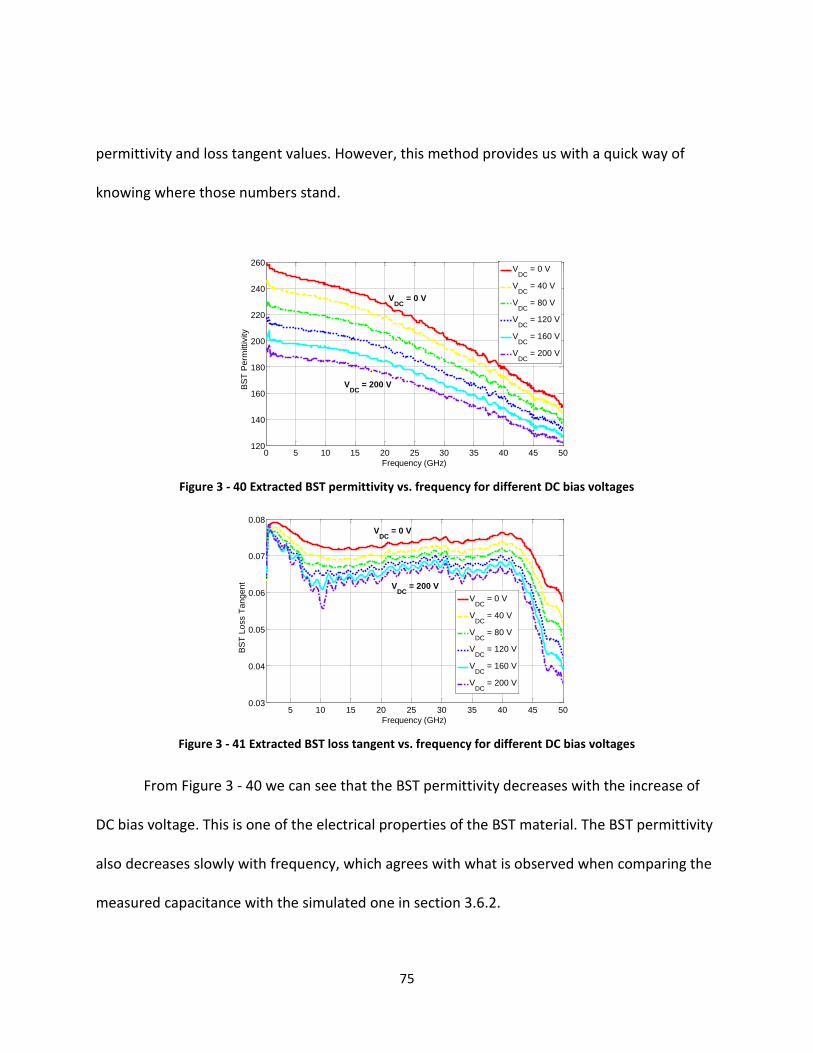
75
permittivity and loss tangent values. However, this method provides us with a quick way of
knowing where those numbers stand.
Figure 3 - 40 Extracted BST permittivity vs. frequency for different DC bias voltages
Figure 3 - 41 Extracted BST loss tangent vs. frequency for different DC bias voltages
From Figure 3 - 40 we can see that the BST permittivity decreases with the increase of
DC bias voltage. This is one of the electrical properties of the BST material. The BST permittivity
also decreases slowly with frequency, which agrees with what is observed when comparing the
measured capacitance with the simulated one in section 3.6.2.
0 5 10 15 20 25 30 35 40 45 50120
140
160
180
200
220
240
260
Frequency (GHz)
BS
T P
erm
ittivity
VDC
= 0 V
VDC
= 40 V
VDC
= 80 V
VDC
= 120 V
VDC
= 160 V
VDC
= 200 V
VDC
= 0 V
VDC
= 200 V
5 10 15 20 25 30 35 40 45 500.03
0.04
0.05
0.06
0.07
0.08
Frequency (GHz)
BS
T L
oss T
an
ge
nt
VDC
= 0 V
VDC
= 40 V
VDC
= 80 V
VDC
= 120 V
VDC
= 160 V
VDC
= 200 V
VDC
= 200 V
VDC
= 0 V
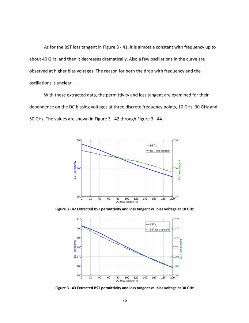
76
As for the BST loss tangent in Figure 3 - 41, it is almost a constant with frequency up to
about 40 GHz, and then it decreases dramatically. Also a few oscillations in the curve are
observed at higher bias voltages. The reason for both the drop with frequency and the
oscillations is unclear.
With these extracted data, the permittivity and loss tangent are examined for their
dependence on the DC biasing voltages at three discrete frequency points, 10 GHz, 30 GHz and
50 GHz. The values are shown in Figure 3 - 42 through Figure 3 - 44.
Figure 3 - 42 Extracted BST permittivity and loss tangent vs. bias voltage at 10 GHz
Figure 3 - 43 Extracted BST permittivity and loss tangent vs. bias voltage at 30 GHz
0 20 40 60 80 100 120 140 160 180 200150
200
250
DC bias voltage (V)
BS
T p
erm
ittivity
0 20 40 60 80 100 120 140 160 180 2000.04
0.06
0.08
BS
T lo
ss t
an
ge
nt
BST r
BST loss tangent
0 20 40 60 80 100 120 140 160 180 200150
160
170
180
190
200
210
DC bias voltage (V)
BS
T p
erm
ittivity
0 20 40 60 80 100 120 140 160 180 2000.064
0.066
0.068
0.07
0.072
0.074
0.076
BS
T lo
ss t
an
ge
nt
BST r
BST loss tangent
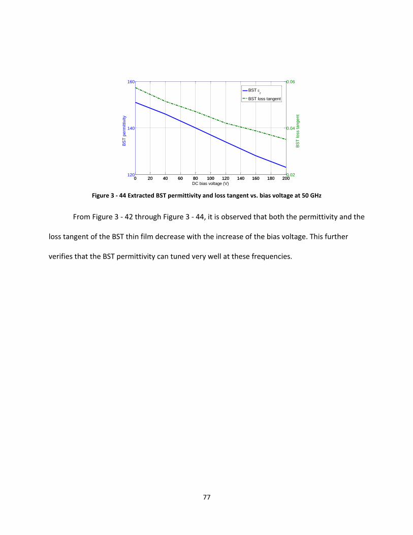
77
Figure 3 - 44 Extracted BST permittivity and loss tangent vs. bias voltage at 50 GHz
From Figure 3 - 42 through Figure 3 - 44, it is observed that both the permittivity and the
loss tangent of the BST thin film decrease with the increase of the bias voltage. This further
verifies that the BST permittivity can tuned very well at these frequencies.
0 20 40 60 80 100 120 140 160 180 200120
140
160
DC bias voltage (V)
BS
T p
erm
ittivity
0 20 40 60 80 100 120 140 160 180 2000.02
0.04
0.06
BS
T lo
ss t
an
ge
nt
BST r
BST loss tangent
78
CHAPTER FOUR: BST-BASED REFLECTARRAY ANTENNA UNIT CELL
A reflectarray antenna is the child of the marriage of a parabolic reflector and a phased
array. Different tuning mechanisms, including varactor, MEMS and BST thick film, have been
investigated and implemented in the past to realize the reflectarray antenna tuning. In this
chapter, we are going to explore the potential of BST thin film being used for tuning the
reflectarray antenna unit cell. The design of the bias lines that can introduce additional loss into
the unit cell is also discussed. This primarily study can be further extended to making
reflectarray antennas on the LCP or other flexible substrates, if combined with the the transfer
technique presented in chapter three.
This chapter is organized as follows. The origin of the reflectarray antennas is first
introduced, followed by a quick overview of the current technologies used for reflectarray
antenna tuning. The design, simulation, fabrication, measurement and results for a BST-thin-
film-based reflectarray antenna unit cell are then presented. The study of the bias line
optimization is carried out as a conclusion for the chapter as well as a prelude for future
research.
79
4.1 Why Reflectarray Antenna?
4.1.1 Advantages and Disadvantages of Parabolic Reflector and Phased Array
A high-gain antenna is a necessity for modern communication systems. Among various
types of antennas, parabolic reflectors and phased arrays are most frequently used in high-gain
applications. Each of these two antennas has its advantages and disadvantages.
A parabolic reflector is named after its physical shape – parabolic – and its working
mechanism – to reflect electromagnetic (EM) waves. It is structurally simple for having one
dish-like main component. This kind of structure doesn’t require complicated power dividing
circuitry and the antenna itself is low loss and highly efficient. However, the curved surface is
hard to build, especially at higher frequencies. Function-wise, the parabolic reflector lacks
electronic beam scanning capability.
On the other hand, a phased array antenna is well-known for its wide-angle beam
steering ability. It consists of an array of radiating elements, and each element is accompanied
by a phase shifter. This array of radiating elements usually takes a linear form (1-dimentional)
or a planar arrangement (2-dimentional). Due to the need of the phase shifters, beam-forming
controllers, amplifier modules and other related circuitry, a phased array antenna can be bulky,
complicated and expensive. Moreover, all these components will contribute to the total loss of
the phased array antenna as well.
A new type of antenna array is needed, which can combine the main advantages of both
a parabolic reflector and a phased array as well as abate the disadvantages of both. This
antenna is named ‘reflectarray antenna’.
80
4.1.2 Reflectarray Antenna
A reflectarray antenna evolves from two traditional antennas: a parabolic reflector and
a phased array. It takes the form of either a flat or a slightly curved reflecting surface made up
of many radiating elements [96]. Like the parabolic reflector, a feed antenna is used to spatially
illuminate the reflectarray antenna elements. Also similar to the phased array, all the
reflectarray antenna elements are designed to reradiate the incident wave in such a way that
the electrical phases in the far-field form a planar phase front. No complicated phase shifters,
power dividers and other circuitry are needed. Different types of antennas can be used as the
radiating elements, for example, printed microstrip patches, open-ended waveguides, dipoles
or rings.
The reflectarray antenna basically inherits the main advantages from both the parabolic
reflector and the phased array antennas. High-gain is an obvious virtue since it is an asset from
both parent antennas. Originating from the parabolic reflector, good efficiency over 50% can be
achieved for a very large aperture. On the other hand, the reflectarray antenna can realize
wide-angle beam steering of 50o and above, the same as the phased array antenna. Also, due to
the elimination of resistive loss generated by the power divider and other related circuitry, the
total loss of the reflectarray antenna is relatively low. Furthermore, the comparably simple
structure allows for easy and low-cost manufacturing, especially in the case of the microstrip-
patch-based reflectarray antenna. An example is shown in Figure 4 - 1. This chapter will be
focused on the investigation of the microstrip-patch-based reflectarray antenna unit cell.
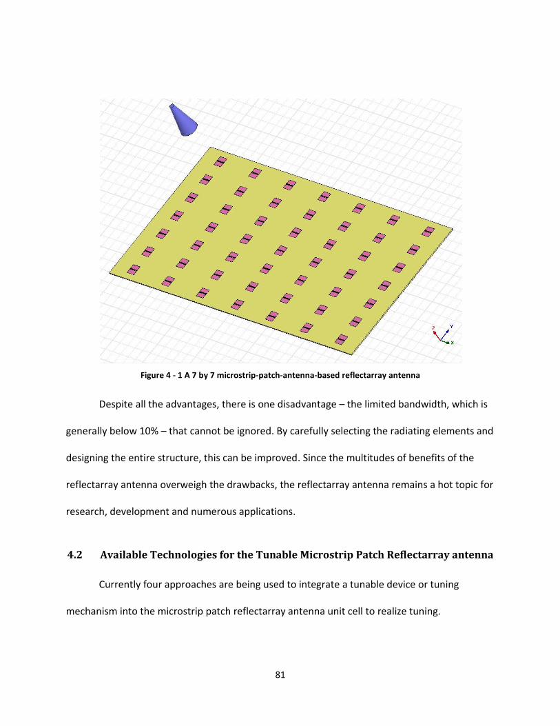
81
Figure 4 - 1 A 7 by 7 microstrip-patch-antenna-based reflectarray antenna
Despite all the advantages, there is one disadvantage – the limited bandwidth, which is
generally below 10% – that cannot be ignored. By carefully selecting the radiating elements and
designing the entire structure, this can be improved. Since the multitudes of benefits of the
reflectarray antenna overweigh the drawbacks, the reflectarray antenna remains a hot topic for
research, development and numerous applications.
4.2 Available Technologies for the Tunable Microstrip Patch Reflectarray antenna
Currently four approaches are being used to integrate a tunable device or tuning
mechanism into the microstrip patch reflectarray antenna unit cell to realize tuning.
82
The first technique is to load varactor diodes in the through-slot located in the middle of
the patch of a unit cell. This variable capacitive loading changes the resonant frequency of the
unit cell, thus realizing beam steering of the array. A phase swing of 320o and a reflection loss of
3.5 dB have been measured at 5.5 GHz with this configuration. [97]
A similar approach is to load a reflectarray antenna unit cell patch with a shunt varactor
diode between the patch and the ground. This has the same effect as changing the resonant
frequency of the unit cell to achieve beam steering of the array. A phase swing of nearly 360o
and a loss of about 2.5 dB have been measured at 5 GHz using this method. [98]
Another technique utilizes a slot in the ground plane loaded with MEMS switches. Using
different configurations of the MEMS switches, the effective slot length can be changed,
leading to a resonant frequency variation and therefore beam steering. A phase swing of nearly
150o and a maximum loss of 1.6 dB have been measured at 2 GHz from this prototype. [99]
The three techniques mentioned above share a common trait: lumped elements, either
varactor diodes or MEMS switches, are used in the configuration. As a result, the operating
frequency is limited by the parasitic effect within the interconnections or the inductive effect of
the bonding wires between the tuning elements and antennas [100]. Therefore, a new
reflectarray antenna unit cell design is needed to eliminate the use of lumped elements while
retaining the tuning ability.
The last technique, also the focus of this chapter, enables tunability without the use of
lumped elements. This reflectarray antenna unit cell design is based on the voltage-dependent
permittivity of BST material. By cutting a through-slot in the middle of the patch in the direction
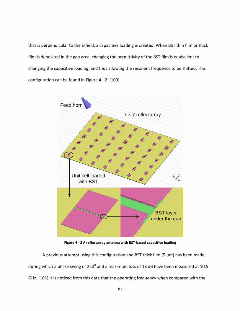
83
that is perpendicular to the E-field, a capacitive loading is created. When BST thin film or thick
film is deposited in the gap area, changing the permittivity of the BST film is equivalent to
changing the capacitive loading, and thus allowing the resonant frequency to be shifted. This
configuration can be found in Figure 4 - 2. [100]
Figure 4 - 2 A reflectarray antenna with BST-based capacitive loading
A previous attempt using this configuration and BST thick film (5 µm) has been made,
during which a phase swing of 250o and a maximum loss of 18 dB have been measured at 10.5
GHz. [101] It is noticed from this data that the operating frequency when compared with the
Feed horn
Unit cell loaded
with BST
7 × 7 reflectarray
BST layer
under the gap

84
cases applying lumped elements has increased from 5 GHz and below to the X-band at 10 GHz.
However, loss performance of 14 – 18 dB is not as satisfactory.
This chapter focuses on improving the loss performance by properly designing the
pattern of BST thin film and bias lines. BST thin film is employed in the unit cell design.
4.3 BST-thin-film-based Reflectarray Antenna Unit Cell Design
The BST-thin-film-based reflectarray antenna unit cell design includes three aspects:
patch size design, BST thin film layout and bias line positions. The patch size generally decides
the resonant frequency; while the BST thin film layout and bias line positions determine the
additional losses that are introduced into the system.
4.3.1 Patch Size Design
The patch size design for the reflectarray antenna unit cell follows the rules of the patch
antenna design [102]. For a rectangular patch with no gap, the width (the dimension
perpendicular to the E field) for getting efficient radiation can be calculated by equation (4 – 1).
( 4 - 1 )
here, c is the velocity of light in free-space, fr is the radiating frequency and εr is the
permittivity of the substrate.
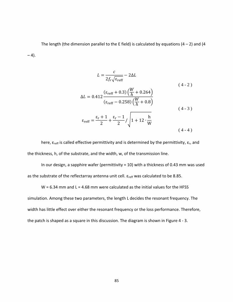
85
The length (the dimension parallel to the E field) is calculated by equations (4 – 2) and (4
– 4).
( 4 - 2 )
( 4 - 3 )
( 4 - 4 )
here, εreff is called effective permittivity and is determined by the permittivity, εr, and
the thickness, h, of the substrate, and the width, w, of the transmission line.
In our design, a sapphire wafer (permittivity = 10) with a thickness of 0.43 mm was used
as the substrate of the reflectarray antenna unit cell. εreff was calculated to be 8.85.
W = 6.34 mm and L = 4.68 mm were calculated as the initial values for the HFSS
simulation. Among these two parameters, the length L decides the resonant frequency. The
width has little effect over either the resonant frequency or the loss performance. Therefore,
the patch is shaped as a square in this discussion. The diagram is shown in Figure 4 - 3.
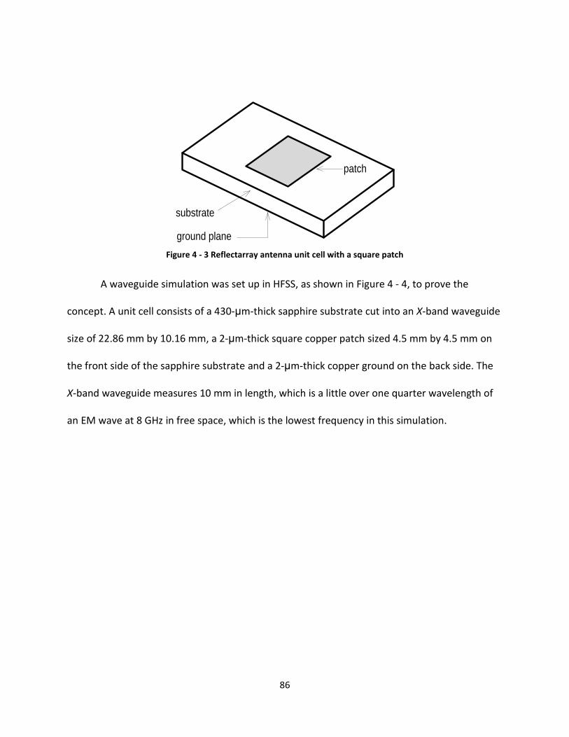
86
Figure 4 - 3 Reflectarray antenna unit cell with a square patch
A waveguide simulation was set up in HFSS, as shown in Figure 4 - 4, to prove the
concept. A unit cell consists of a 430-μm-thick sapphire substrate cut into an X-band waveguide
size of 22.86 mm by 10.16 mm, a 2-μm-thick square copper patch sized 4.5 mm by 4.5 mm on
the front side of the sapphire substrate and a 2-μm-thick copper ground on the back side. The
X-band waveguide measures 10 mm in length, which is a little over one quarter wavelength of
an EM wave at 8 GHz in free space, which is the lowest frequency in this simulation.
substrate
patch
BSTgap
ground plane
substrate
patch
Lumped C
gap
ground plane
substrate
patch
ground plane
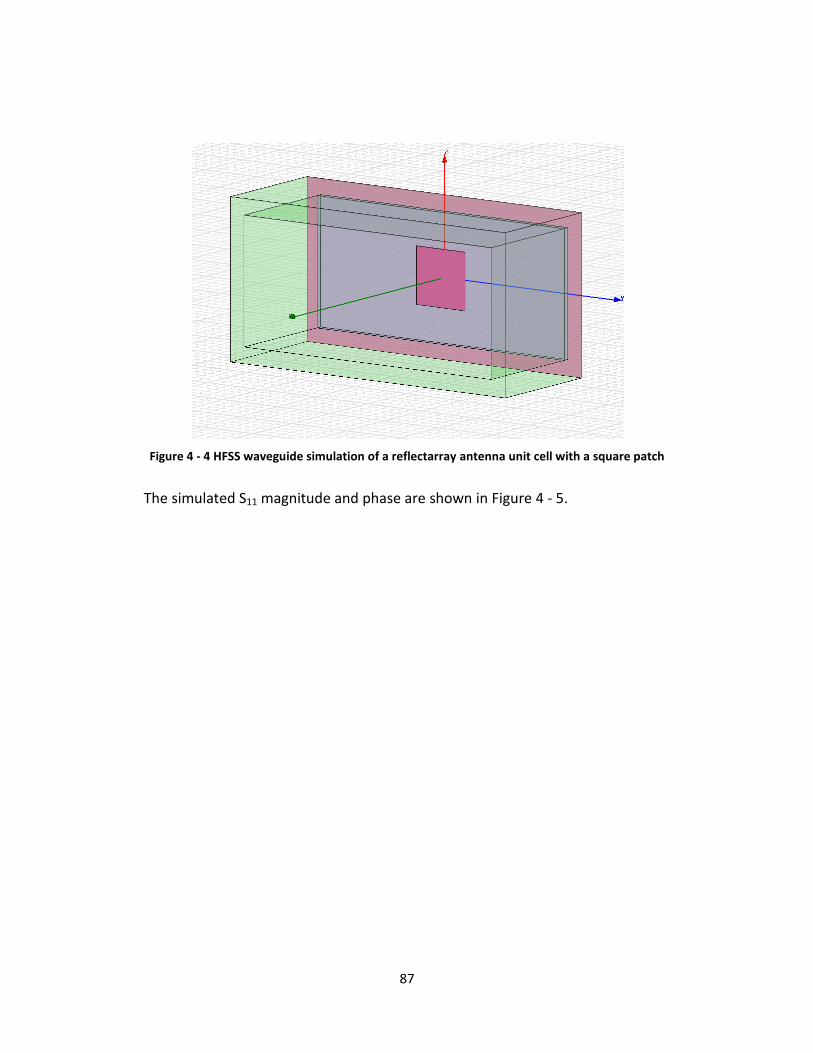
87
Figure 4 - 4 HFSS waveguide simulation of a reflectarray antenna unit cell with a square patch
The simulated S11 magnitude and phase are shown in Figure 4 - 5.
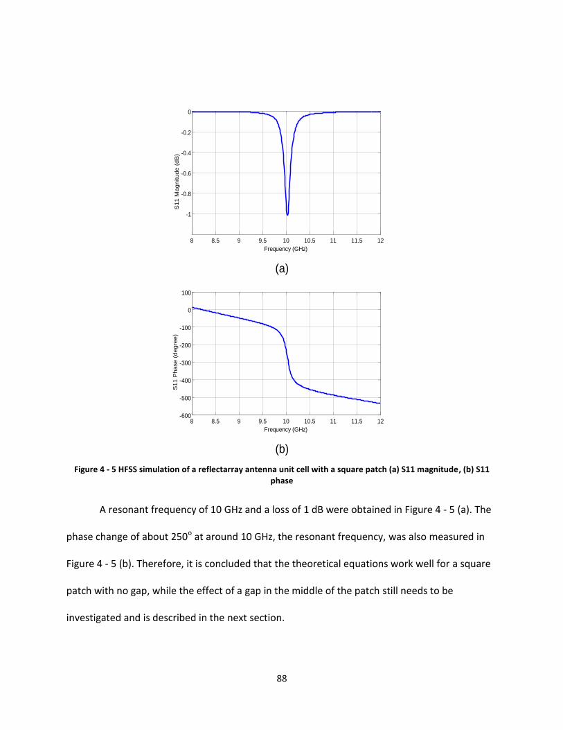
88
Figure 4 - 5 HFSS simulation of a reflectarray antenna unit cell with a square patch (a) S11 magnitude, (b) S11 phase
A resonant frequency of 10 GHz and a loss of 1 dB were obtained in Figure 4 - 5 (a). The
phase change of about 250o at around 10 GHz, the resonant frequency, was also measured in
Figure 4 - 5 (b). Therefore, it is concluded that the theoretical equations work well for a square
patch with no gap, while the effect of a gap in the middle of the patch still needs to be
investigated and is described in the next section.
(a)
(b)
8 8.5 9 9.5 10 10.5 11 11.5 12
-1
-0.8
-0.6
-0.4
-0.2
0
Frequency (GHz)
S1
1 M
ag
nitu
de
(d
B)
8 8.5 9 9.5 10 10.5 11 11.5 12-600
-500
-400
-300
-200
-100
0
100
Frequency (GHz)
S1
1 P
ha
se
(d
eg
ree
)
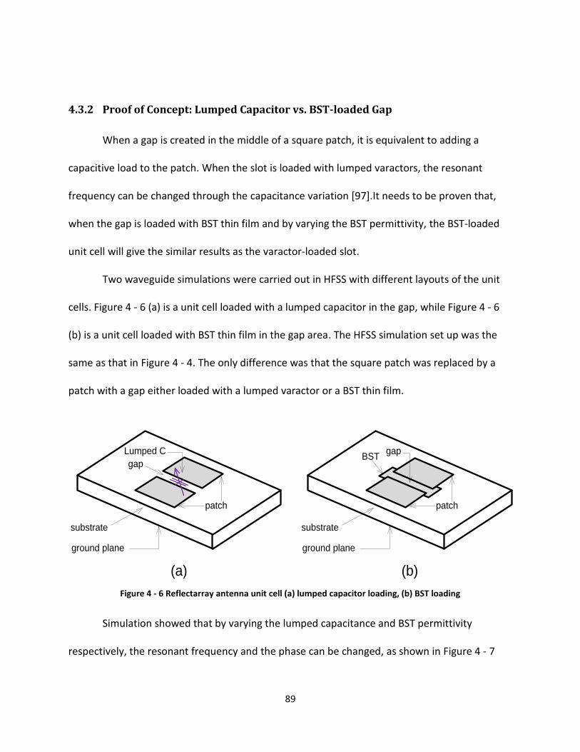
89
4.3.2 Proof of Concept: Lumped Capacitor vs. BST-loaded Gap
When a gap is created in the middle of a square patch, it is equivalent to adding a
capacitive load to the patch. When the slot is loaded with lumped varactors, the resonant
frequency can be changed through the capacitance variation [97].It needs to be proven that,
when the gap is loaded with BST thin film and by varying the BST permittivity, the BST-loaded
unit cell will give the similar results as the varactor-loaded slot.
Two waveguide simulations were carried out in HFSS with different layouts of the unit
cells. Figure 4 - 6 (a) is a unit cell loaded with a lumped capacitor in the gap, while Figure 4 - 6
(b) is a unit cell loaded with BST thin film in the gap area. The HFSS simulation set up was the
same as that in Figure 4 - 4. The only difference was that the square patch was replaced by a
patch with a gap either loaded with a lumped varactor or a BST thin film.
Figure 4 - 6 Reflectarray antenna unit cell (a) lumped capacitor loading, (b) BST loading
Simulation showed that by varying the lumped capacitance and BST permittivity
respectively, the resonant frequency and the phase can be changed, as shown in Figure 4 - 7
substrate
patch
BSTgap
ground plane
substrate
patch
Lumped C
gap
ground plane
substrate
patch
ground plane
(a) (b)
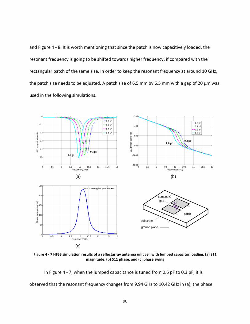
90
and Figure 4 - 8. It is worth mentioning that since the patch is now capacitively loaded, the
resonant frequency is going to be shifted towards higher frequency, if compared with the
rectangular patch of the same size. In order to keep the resonant frequency at around 10 GHz,
the patch size needs to be adjusted. A patch size of 6.5 mm by 6.5 mm with a gap of 20 µm was
used in the following simulations.
Figure 4 - 7 HFSS simulation results of a reflectarray antenna unit cell with lumped capacitor loading. (a) S11 magnitude, (b) S11 phase, and (c) phase swing
In Figure 4 - 7, when the lumped capacitance is tuned from 0.6 pF to 0.3 pF, it is
observed that the resonant frequency changes from 9.94 GHz to 10.42 GHz in (a), the phase
8 8.5 9 9.5 10 10.5 11 11.5 12
-0.5
-0.4
-0.3
-0.2
-0.1
0
Frequency (GHz)
S1
1 m
ag
nitu
de
(d
B)
0.3 pF
0.4 pF
0.5 pF
0.6 pF
0.6 pF
0.3 pF
8 8.5 9 9.5 10 10.5 11 11.5 12-1200
-1000
-800
-600
-400
-200
Frequency (GHz)
S1
1 p
ha
se
(d
eg
ree
)
0.3 pF
0.4 pF
0.5 pF
0.6 pF
0.3 pF0.6 pF
8 8.5 9 9.5 10 10.5 11 11.5 120
50
100
150
200
250
Frequency (GHz)
Ph
ase
sw
ing
(d
eg
ree
)
Max = 233 degrees @ 10.17 GHz
(a) (b)
(c)
substrate
patch
Lumped C
gap
ground plane
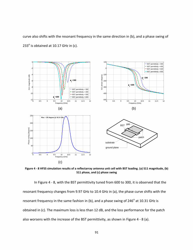
91
curve also shifts with the resonant frequency in the same direction in (b), and a phase swing of
233o is obtained at 10.17 GHz in (c).
Figure 4 - 8 HFSS simulation results of a reflectarray antenna unit cell with BST loading. (a) S11 magnitude, (b) S11 phase, and (c) phase swing
In Figure 4 - 8, with the BST permittivity tuned from 600 to 300, it is observed that the
resonant frequency changes from 9.97 GHz to 10.4 GHz in (a), the phase curve shifts with the
resonant frequency in the same fashion in (b), and a phase swing of 246o at 10.31 GHz is
obtained in (c). The maximum loss is less than 12 dB, and the loss performance for the patch
also worsens with the increase of the BST permittivity, as shown in Figure 4 - 8 (a).
8 8.5 9 9.5 10 10.5 11 11.5 120
50
100
150
200
250
Frequency (GHz)
Ph
ase
sw
ing
(d
eg
ree
)
Max = 245 degrees @ 10.31 GHz
(a) (b)
(c)
substrate
patch
BSTgap
ground plane
8 8.5 9 9.5 10 10.5 11 11.5 12-12
-10
-8
-6
-4
-2
0
Frequency (GHz)
S1
1 m
ag
nitu
de
(d
B)
BST permittivity = 300
BST permittivity = 400
BST permittivity = 500
BST permittivity = 600r=600
r=300
8 8.5 9 9.5 10 10.5 11 11.5 12-500
-400
-300
-200
-100
0
100
Frequency (GHz)S
11
ph
ase
(d
eg
ree
)
BST permittivity = 300
BST permittivity = 400
BST permittivity = 500
BST permittivity = 600
r=600
r=300
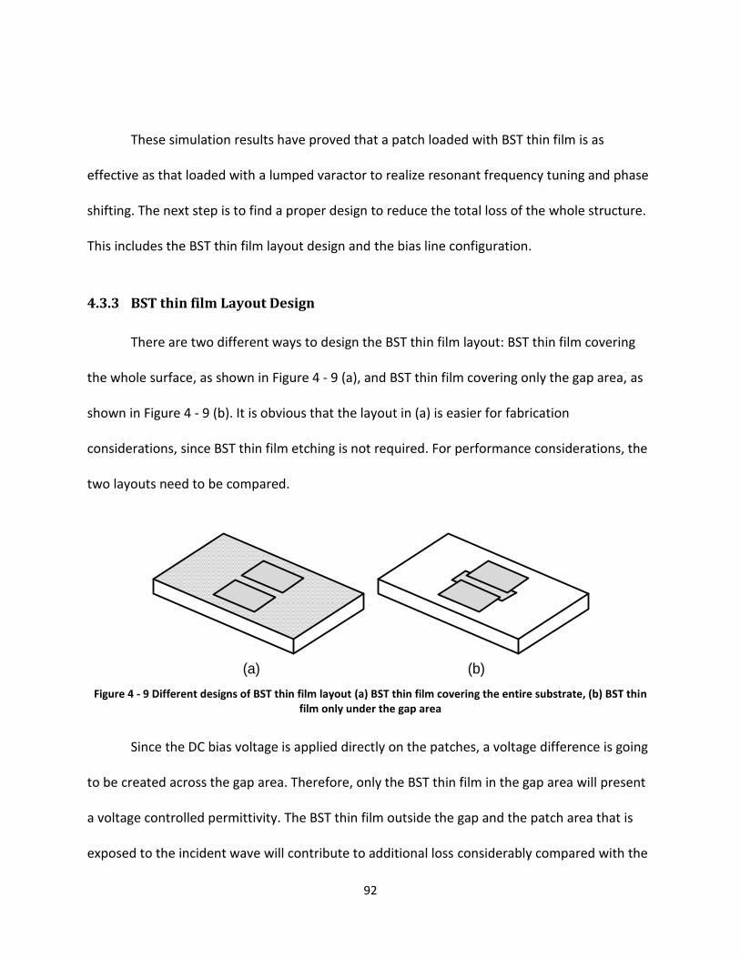
92
These simulation results have proved that a patch loaded with BST thin film is as
effective as that loaded with a lumped varactor to realize resonant frequency tuning and phase
shifting. The next step is to find a proper design to reduce the total loss of the whole structure.
This includes the BST thin film layout design and the bias line configuration.
4.3.3 BST thin film Layout Design
There are two different ways to design the BST thin film layout: BST thin film covering
the whole surface, as shown in Figure 4 - 9 (a), and BST thin film covering only the gap area, as
shown in Figure 4 - 9 (b). It is obvious that the layout in (a) is easier for fabrication
considerations, since BST thin film etching is not required. For performance considerations, the
two layouts need to be compared.
Figure 4 - 9 Different designs of BST thin film layout (a) BST thin film covering the entire substrate, (b) BST thin film only under the gap area
Since the DC bias voltage is applied directly on the patches, a voltage difference is going
to be created across the gap area. Therefore, only the BST thin film in the gap area will present
a voltage controlled permittivity. The BST thin film outside the gap and the patch area that is
exposed to the incident wave will contribute to additional loss considerably compared with the
(c)
(b)(a)
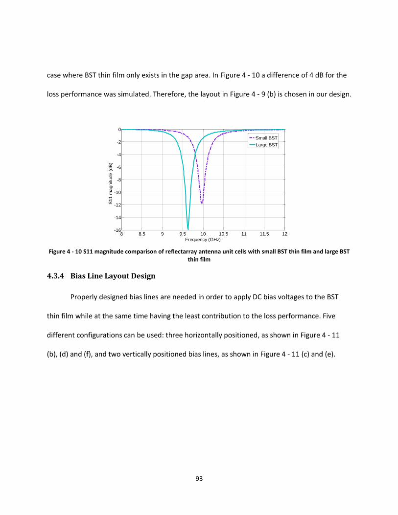
93
case where BST thin film only exists in the gap area. In Figure 4 - 10 a difference of 4 dB for the
loss performance was simulated. Therefore, the layout in Figure 4 - 9 (b) is chosen in our design.
Figure 4 - 10 S11 magnitude comparison of reflectarray antenna unit cells with small BST thin film and large BST thin film
4.3.4 Bias Line Layout Design
Properly designed bias lines are needed in order to apply DC bias voltages to the BST
thin film while at the same time having the least contribution to the loss performance. Five
different configurations can be used: three horizontally positioned, as shown in Figure 4 - 11
(b), (d) and (f), and two vertically positioned bias lines, as shown in Figure 4 - 11 (c) and (e).
8 8.5 9 9.5 10 10.5 11 11.5 12-16
-14
-12
-10
-8
-6
-4
-2
0
Frequency (GHz)
S1
1 m
ag
nitu
de
(d
B)
Small BST
Large BST
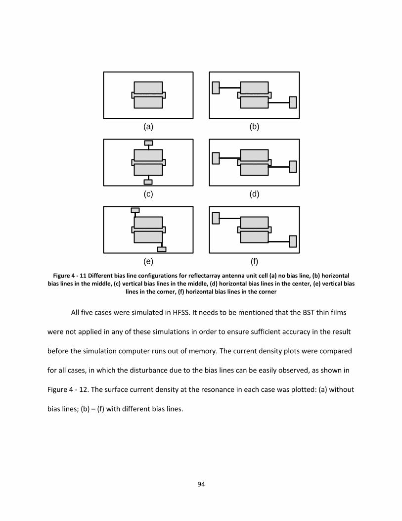
94
Figure 4 - 11 Different bias line configurations for reflectarray antenna unit cell (a) no bias line, (b) horizontal bias lines in the middle, (c) vertical bias lines in the middle, (d) horizontal bias lines in the center, (e) vertical bias
lines in the corner, (f) horizontal bias lines in the corner
All five cases were simulated in HFSS. It needs to be mentioned that the BST thin films
were not applied in any of these simulations in order to ensure sufficient accuracy in the result
before the simulation computer runs out of memory. The current density plots were compared
for all cases, in which the disturbance due to the bias lines can be easily observed, as shown in
Figure 4 - 12. The surface current density at the resonance in each case was plotted: (a) without
bias lines; (b) – (f) with different bias lines.
(b)(a)
(d)(c)
(f)(e)
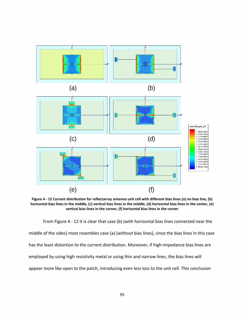
95
Figure 4 - 12 Current distribution for reflectarray antenna unit cell with different bias lines (a) no bias line, (b) horizontal bias lines in the middle, (c) vertical bias lines in the middle, (d) horizontal bias lines in the center, (e)
vertical bias lines in the corner, (f) horizontal bias lines in the corner
From Figure 4 - 12 it is clear that case (b) (with horizontal bias lines connected near the
middle of the sides) most resembles case (a) (without bias lines), since the bias lines in this case
has the least distortion to the current distribution. Moreover, if high-impedance bias lines are
employed by using high resistivity metal or using thin and narrow lines, the bias lines will
appear more like open to the patch, introducing even less loss to the unit cell. This conclusion
(b)(a)
(d)(c)
(f)(e)
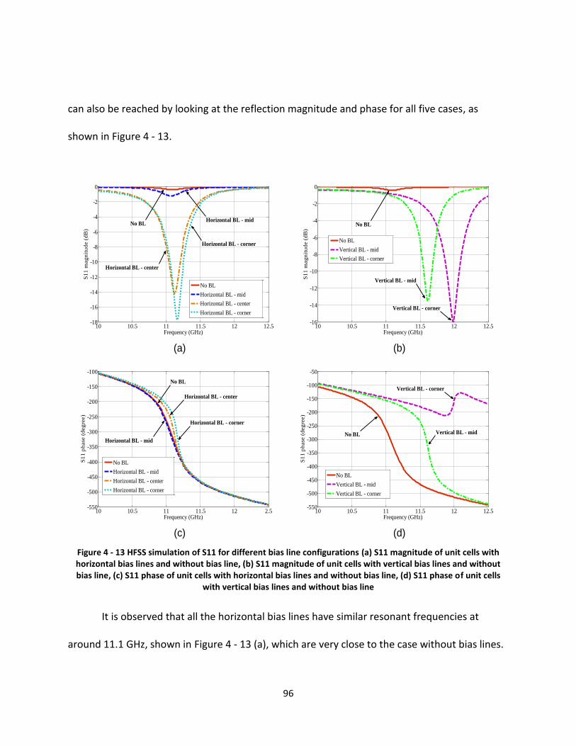
96
can also be reached by looking at the reflection magnitude and phase for all five cases, as
shown in Figure 4 - 13.
Figure 4 - 13 HFSS simulation of S11 for different bias line configurations (a) S11 magnitude of unit cells with horizontal bias lines and without bias line, (b) S11 magnitude of unit cells with vertical bias lines and without bias line, (c) S11 phase of unit cells with horizontal bias lines and without bias line, (d) S11 phase of unit cells
with vertical bias lines and without bias line
It is observed that all the horizontal bias lines have similar resonant frequencies at
around 11.1 GHz, shown in Figure 4 - 13 (a), which are very close to the case without bias lines.
10 10.5 11 11.5 12 12.5-18
-16
-14
-12
-10
-8
-6
-4
-2
0
Frequency (GHz)
S1
1 m
ag
nit
ud
e (
dB
)
No BL
Horizontal BL - mid
Horizontal BL - center
Horizontal BL - corner
No BLHorizontal BL - mid
Horizontal BL - corner
Horizontal BL - center
10 10.5 11 11.5 12 12.5-16
-14
-12
-10
-8
-6
-4
-2
0
Frequency (GHz)
S1
1 m
ag
nit
ud
e (
dB
)
No BL
Vertical BL - mid
Vertical BL - corner
Vertical BL - corner
Vertical BL - mid
No BL
10 10.5 11 11.5 12 2.5-550
-500
-450
-400
-350
-300
-250
-200
-150
-100
Frequency (GHz)
S1
1 p
hase
(d
eg
ree)
No BL
Horizontal BL - mid
Horizontal BL - center
Horizontal BL - corner
Horizontal BL - mid
Horizontal BL - center
Horizontal BL - corner
No BL
10 10.5 11 11.5 12 12.5-550
-500
-450
-400
-350
-300
-250
-200
-150
-100
-50
Frequency (GHz)
S1
1 p
hase
(d
eg
ree)
No BL
Vertical BL - mid
Vertical BL - corner
No BL Vertical BL - mid
Vertical BL - corner
(b)(a)
(d)(c)
97
A large phase change at resonance is also obtained for each case, as shown in Figure 4 - 13 (c).
The difference in loss can reach as much as 18 dB for the different bias line positions. Vertical
bias line cases not only show a large loss at resonance, as shown in Figure 4 - 13 (b), but also
show a resonant frequency difference of at least 500 MHz compared to the case without bias
lines, as shown in Figure 4 - 13 (d). One case with vertical bias lines in the middle of the patch
also shows a much smaller phase change compared to the other cases. Therefore, it is
concluded that the horizontal bias lines do not affect the resonant frequency, while the vertical
bias lines do. Moreover, the position of the horizontal bias lines is very important. In the case
without BST thin film, bias lines positioned in the middle along the side of each half-patch give
the least additional loss, less than 1 dB to be exact. It should be pointed out that since these
structures were simulated without BST thin film, the resonant frequency shifted from 10 GHz to
around 11 GHz.
Using the patch size (6.5 mm by 6.5 mm with 20 µm gap), the BST layout (only in the gap
area) and the bias line arrangement (in the middle of each half patch) discussed above, the unit
cell simulation was performed for the X-band.
4.4 X-band Reflectarray Antenna Unit Cell Simulation
An X-band reflectarray antenna unit cell was simulated in HFSS with the BST permittivity
being the only variable, as shown in Figure 4 - 14. A 430-μm-thick sapphire substrate is placed
at the end of an X-band waveguide of 10 mm in length. The front side of the sapphire substrate
has a copper patch with a 20-µm gap cut horizontally across the middle, a BST thin film in the
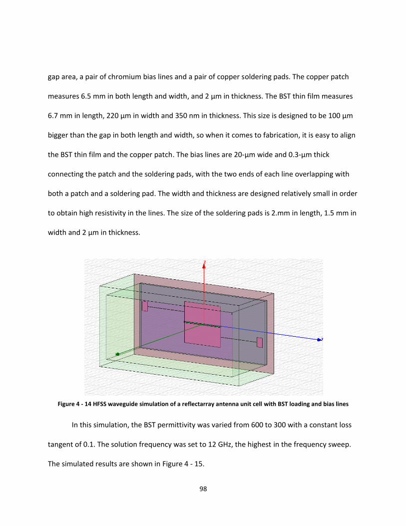
98
gap area, a pair of chromium bias lines and a pair of copper soldering pads. The copper patch
measures 6.5 mm in both length and width, and 2 µm in thickness. The BST thin film measures
6.7 mm in length, 220 µm in width and 350 nm in thickness. This size is designed to be 100 µm
bigger than the gap in both length and width, so when it comes to fabrication, it is easy to align
the BST thin film and the copper patch. The bias lines are 20-µm wide and 0.3-µm thick
connecting the patch and the soldering pads, with the two ends of each line overlapping with
both a patch and a soldering pad. The width and thickness are designed relatively small in order
to obtain high resistivity in the lines. The size of the soldering pads is 2.mm in length, 1.5 mm in
width and 2 µm in thickness.
Figure 4 - 14 HFSS waveguide simulation of a reflectarray antenna unit cell with BST loading and bias lines
In this simulation, the BST permittivity was varied from 600 to 300 with a constant loss
tangent of 0.1. The solution frequency was set to 12 GHz, the highest in the frequency sweep.
The simulated results are shown in Figure 4 - 15.
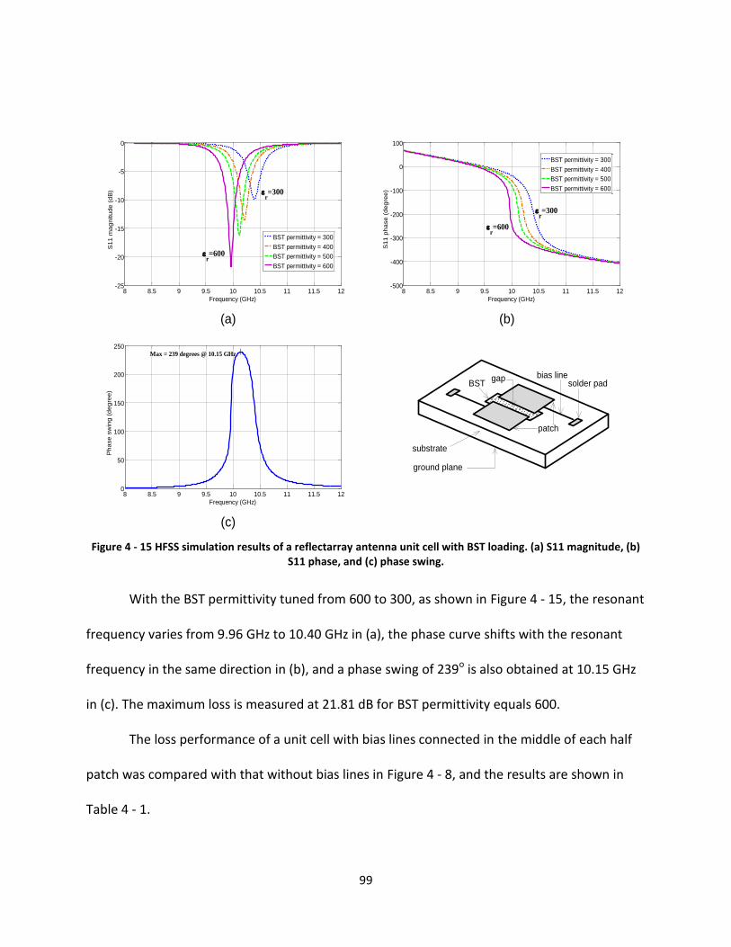
99
Figure 4 - 15 HFSS simulation results of a reflectarray antenna unit cell with BST loading. (a) S11 magnitude, (b) S11 phase, and (c) phase swing.
With the BST permittivity tuned from 600 to 300, as shown in Figure 4 - 15, the resonant
frequency varies from 9.96 GHz to 10.40 GHz in (a), the phase curve shifts with the resonant
frequency in the same direction in (b), and a phase swing of 239o is also obtained at 10.15 GHz
in (c). The maximum loss is measured at 21.81 dB for BST permittivity equals 600.
The loss performance of a unit cell with bias lines connected in the middle of each half
patch was compared with that without bias lines in Figure 4 - 8, and the results are shown in
Table 4 - 1.
(a) (b)
(c)
substrate
patch
BSTgap
ground plane
solder padbias line
8 8.5 9 9.5 10 10.5 11 11.5 12-25
-20
-15
-10
-5
0
Frequency (GHz)
S1
1 m
ag
nitu
de
(d
B)
BST permittivity = 300
BST permittivity = 400
BST permittivity = 500
BST permittivity = 600
r=600
r=300
8 8.5 9 9.5 10 10.5 11 11.5 12-500
-400
-300
-200
-100
0
100
Frequency (GHz)
S1
1 p
ha
se
(d
eg
ree
)
BST permittivity = 300
BST permittivity = 400
BST permittivity = 500
BST permittivity = 600
r=300
r=600
8 8.5 9 9.5 10 10.5 11 11.5 120
50
100
150
200
250
Frequency (GHz)
Ph
ase
sw
ing
(d
eg
ree
)
Max = 239 degrees @ 10.15 GHz
100
Table 4 - 1 Compare loss performance of reflectarray antenna unit cells with and without bias lines
Max. Loss for Simulated Reflectarray
Unit Cell with Bias Lines (Mid)
Max. Loss for Simulated Reflectarray Unit Cell without Bias
Lines
Additional Loss Caused by Optimized Bias
Lines
BST permittivity = 600
21.81 dB @ 9.96 GHz 11.89 dB @ 9.97 GHz 9.92 dB
BST permittivity = 500
16.27 dB @ 10.12 GHz 10.59 dB @ 10.05 GHz 5.68 dB
BST permittivity = 400
13.57 dB @ 10.21 GHz 8.84 dB @ 10.19 GHz 4.73 dB
BST permittivity = 300
9.97 dB @ 10.40 GHz 6.52 dB @ 10.44 GHz 3.45 dB
From this comparison it is clear that the bias lines introduced nearly 10 dB of additional
loss when BST permittivity equals 600, which is different than what has been concluded in
section 4.3.4 that a good bias line design should add in no more than 1 dB of loss. The reason
for this discrepancy was found during a further study of the bias line positions, which will be
discussed in section 4.8.
4.5 X-band Reflectarray Antenna Unit Cell Fabrication
A BST-based reflectarray antenna unit cell was fabricated following the steps illustrated
in Figure 4 - 16. A sapphire wafer was first cut into a size of 22.86 mm by 10.16 mm, the same
size as the cross section of an X-band waveguide. A 350-nm-thick BST thin-film was deposited
using RF magnetron sputtering with a substrate temperature of 400 oC. It needs to be
mentioned that this temperature is different from the one used in section 3.4, which was 650
oC on a silicon substrate. The reason is that a different substrate – sapphire – was used in the
101
reflectarray antenna unit cell fabrication. Sapphire has a CTE of around 10, which is very close
to that of the BST material. So the thermal mismatch problem during the annealing process no
longer exists. Therefore, the BST thin film on a sapphire substrate can be deposited at a lower
temperature (400 oC) and then annealed at a higher temperature (900 oC, due to our
equipment limitations).
After the BST thin film was deposited, Shipley 1813 (spun at a rate of 3000 rpm) was
used as an etching mask for wet-etching the BST thin film. A commercially available HF solution
diluted to 1% was used as an etchant. This concentration was different from that used in
section 3.4, which was 2%. Since the BST thin film was deposited at lower temperature, 400 oC
in this case, its etching was relatively easy. In order to have clearly defined patterns, the etching
rate needs to be controlled within a limit so that over-etching can be prevented. The 1%
solution etched the BST thin film in about 5 minutes and the patterns looked very neat when
checked under a microscope. Also as mentioned before, the BST thin film was sized 200 µm
larger than the gap in both length and width. This oversize approach can alleviate the negative
effects from the misalignment in photolithographic process as well as the possible over-etching
of the BST thin film.
After the substrate with etched BST thin film was rinsed using acetone-methanol-DI
water and cleaned in a plasma asher, it was annealed at 900o for 20 hours in a box oven with an
oxygen flow under atmospheric pressure. This annealing process had to happen after BST
etching since the annealed BST thin film is very resistant to etchant.
102
After annealing, chromium bias lines of 20 um wide and 300 nm thick were then
deposited and patterned using liftoff. Shipley 1813 (spun at 3000 rpm) was again used. The
resistance of each bias line measured about 3 kΩ using a digital multimeter. The sequence of
bias line deposition and patch deposition could not be altered. The bias lines were designed at
300-nm thick, while the patch was designed at 2 µm thick. The overlaps between the bias lines
and the patch were also needed to ensure good electrical connection. If the bias lines were
deposited first, followed by the patch deposition, the thick patch pattern could easily cover the
thin bias lines in the areas where the two overlapped. If this process were reversed, the thin
bias lines were going to be disconnected at the 2-µm step of the patch edge.
After the bias lines were defined, a patch and a pair of soldering pads made of a Cr-Cu-
Cr (30nm-1.8µm-150nm) multilayer with a total thickness of around 2 µm were deposited in an
E-beam evaporator without breaking the vacuum, and patterned by liftoff. AZ 4620 was used as
the PR in the lift-off process, since it can provide a thickness of at least several microns,
depending on the spin speed. In our work, 3000 rpm was used, which created a PR thick film of
about 8 µm. By now, the front side of the unit cell has been completed. On the back side of the
substrate, the ground plane, a copper layer of 2 µm was deposited using E-beam evaporator.
This concluded the fabrication of a reflectarray antenna unit cell. The detailed recipe for
each step is also listed in Appendix D. Wires for connecting the unit cell with a DC power supply
will be soldered onto the soldering pads before taking measurement.
103
Figure 4 - 16 Reflectarray antenna unit cell fabrication procedure for the front side
The fabricated BST-based reflectarray antenna unit cell was checked under a
microscope. A close view of the BST thin film and the gap is shown in Figure 4 - 17.
Sapphire wafer is cut to the
size of an X-band waveguide.
BST thin film is deposited onto
the sapphire substrate.
BST thin film is etched in
diluted HF solution.
Cr bias lines are deposited and
patterned using lift-off.
A copper patch and solder pads
are deposited and patterned
using lift-off. A copper ground is
also deposited on the back of
the substrate.
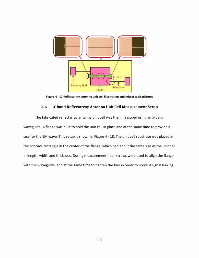
104
Figure 4 - 17 Reflectarray antenna unit cell illustration and microscopic pictures
4.6 X-band Reflectarray Antenna Unit Cell Measurement Setup
The fabricated reflectarray antenna unit cell was then measured using an X-band
waveguide. A flange was built to hold the unit cell in place and at the same time to provide a
seal for the EM wave. This setup is shown in Figure 4 - 18. The unit cell substrate was placed in
the concave rectangle in the center of the flange, which had about the same size as the unit cell
in length, width and thickness. During measurement, four screws were used to align the flange
with the waveguide, and at the same time to tighten the two in order to prevent signal leaking.
BST
Patch
Soldering PadBias Line
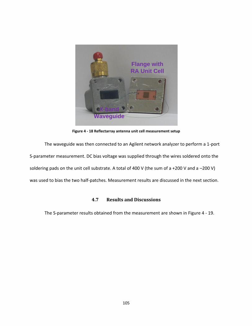
105
Figure 4 - 18 Reflectarray antenna unit cell measurement setup
The waveguide was then connected to an Agilent network analyzer to perform a 1-port
S-parameter measurement. DC bias voltage was supplied through the wires soldered onto the
soldering pads on the unit cell substrate. A total of 400 V (the sum of a +200 V and a –200 V)
was used to bias the two half-patches. Measurement results are discussed in the next section.
4.7 Results and Discussions
The S-parameter results obtained from the measurement are shown in Figure 4 - 19.
X-band
Waveguide
Flange with
RA Unit Cell
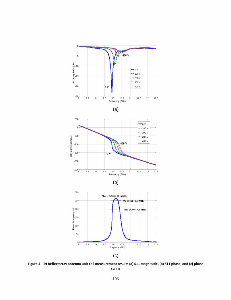
106
Figure 4 - 19 Reflectarray antenna unit cell measurement results (a) S11 magnitude, (b) S11 phase, and (c) phase swing
(a)
(b)
(c)
8 8.5 9 9.5 10 10.5 11 11.5 12 12.5-25
-20
-15
-10
-5
0
Frequency (GHz)
S1
1 m
ag
nitu
de
(d
B)
0 V
100 V
200 V
300 V
400 V0 V
400 V
8 8.5 9 9.5 10 10.5 11 11.5 12 12.5-1000
-800
-600
-400
-200
0
200
Frequency (GHz)
S1
1 p
ha
se
(d
eg
ree
)
0 V
100 V
200 V
300 V
400 V400 V
0 V
8 8.5 9 9.5 10 10.5 11 11.5 12 12.50
50
100
150
200
250
300
Frequency (GHz)
Ph
ase
Sw
ing
(d
eg
ree)
Max = 262.8 @ 10.15 GHz
BW @ 250 = 240 MHz
BW @ 200 = 420 MHz
107
It is observed from Figure 4 - 19 (a) that the unit cell exhibits a maximum loss of 23 dB
when biased at 0 V and 3.6 dB when biased at 400 V. The losses at the resonant frequency
decrease with different bias voltages. The total loss is less than 10 dB when a DC bias voltage of
100 V (equivalent to 5 V/um) and above is applied, which is at least 4 dB better than the
previous attempt [101]. The resonance frequency of the patch increases from 9.93 GHz to 10.45
GHz, corresponding to a DC bias voltage increase of 0-400 V (equivalent to 20 V/um).
The measured reflection phase is plotted in Figure 4 - 19 (b). It is observed that varying
the DC bias voltage across the gap can cause the reflection phase of the unit cell to change. This
phenomenon is the key for designing a large-scale reflectarray antenna using BST-tuning.
Figure 4 - 19 (c) shows the maximum phase swing at different frequencies. This
maximum phase swing is calculated from the phase difference between 0 and 400 V biasing. A
maximum phase swing of 263 degree is obtained at 10.15 GHz, and a bandwidth of 240 MHz for
a phase shift greater than 250 degrees is also obtained.
The measured loss performance is also compared with the simulated one, as shown in
Table 4 - 2.
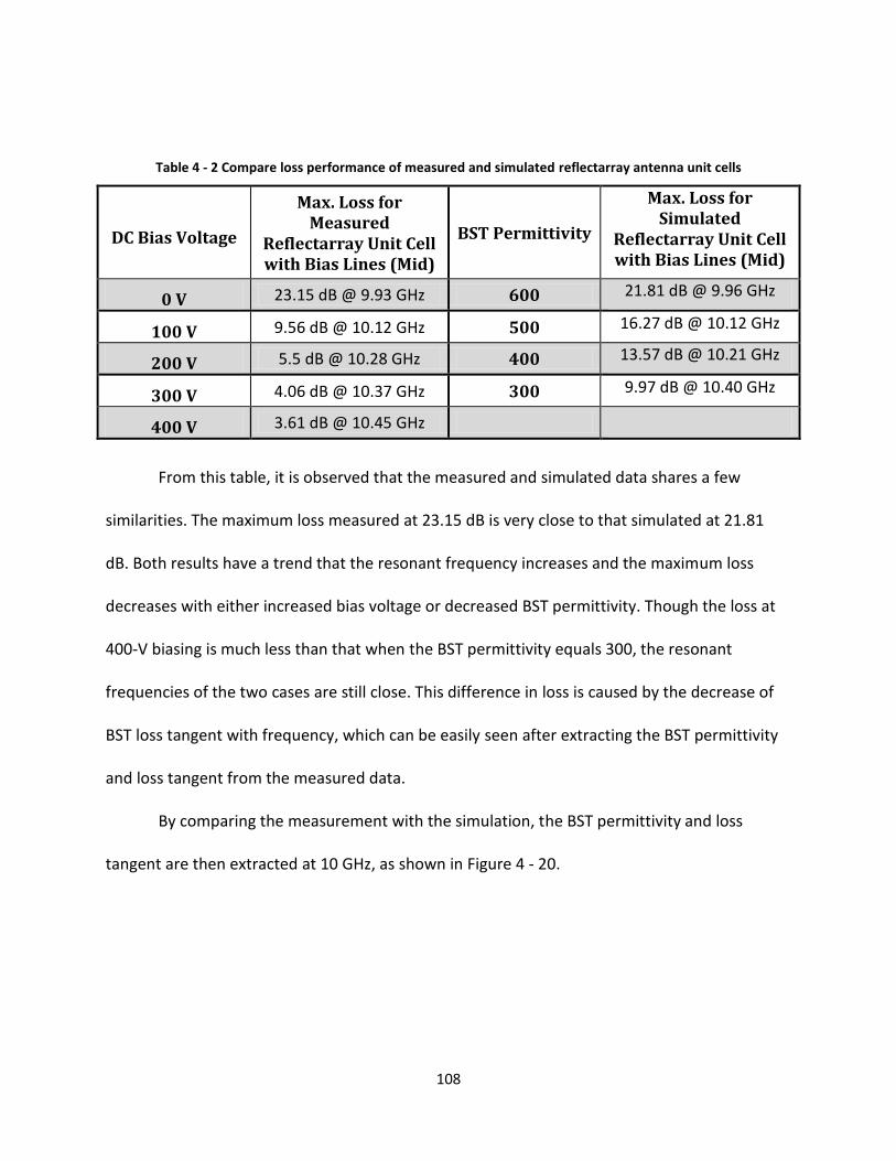
108
Table 4 - 2 Compare loss performance of measured and simulated reflectarray antenna unit cells
DC Bias Voltage
Max. Loss for Measured
Reflectarray Unit Cell with Bias Lines (Mid)
BST Permittivity
Max. Loss for Simulated
Reflectarray Unit Cell with Bias Lines (Mid)
0 V 23.15 dB @ 9.93 GHz 600 21.81 dB @ 9.96 GHz
100 V 9.56 dB @ 10.12 GHz 500 16.27 dB @ 10.12 GHz
200 V 5.5 dB @ 10.28 GHz 400 13.57 dB @ 10.21 GHz
300 V 4.06 dB @ 10.37 GHz 300 9.97 dB @ 10.40 GHz
400 V 3.61 dB @ 10.45 GHz
From this table, it is observed that the measured and simulated data shares a few
similarities. The maximum loss measured at 23.15 dB is very close to that simulated at 21.81
dB. Both results have a trend that the resonant frequency increases and the maximum loss
decreases with either increased bias voltage or decreased BST permittivity. Though the loss at
400-V biasing is much less than that when the BST permittivity equals 300, the resonant
frequencies of the two cases are still close. This difference in loss is caused by the decrease of
BST loss tangent with frequency, which can be easily seen after extracting the BST permittivity
and loss tangent from the measured data.
By comparing the measurement with the simulation, the BST permittivity and loss
tangent are then extracted at 10 GHz, as shown in Figure 4 - 20.
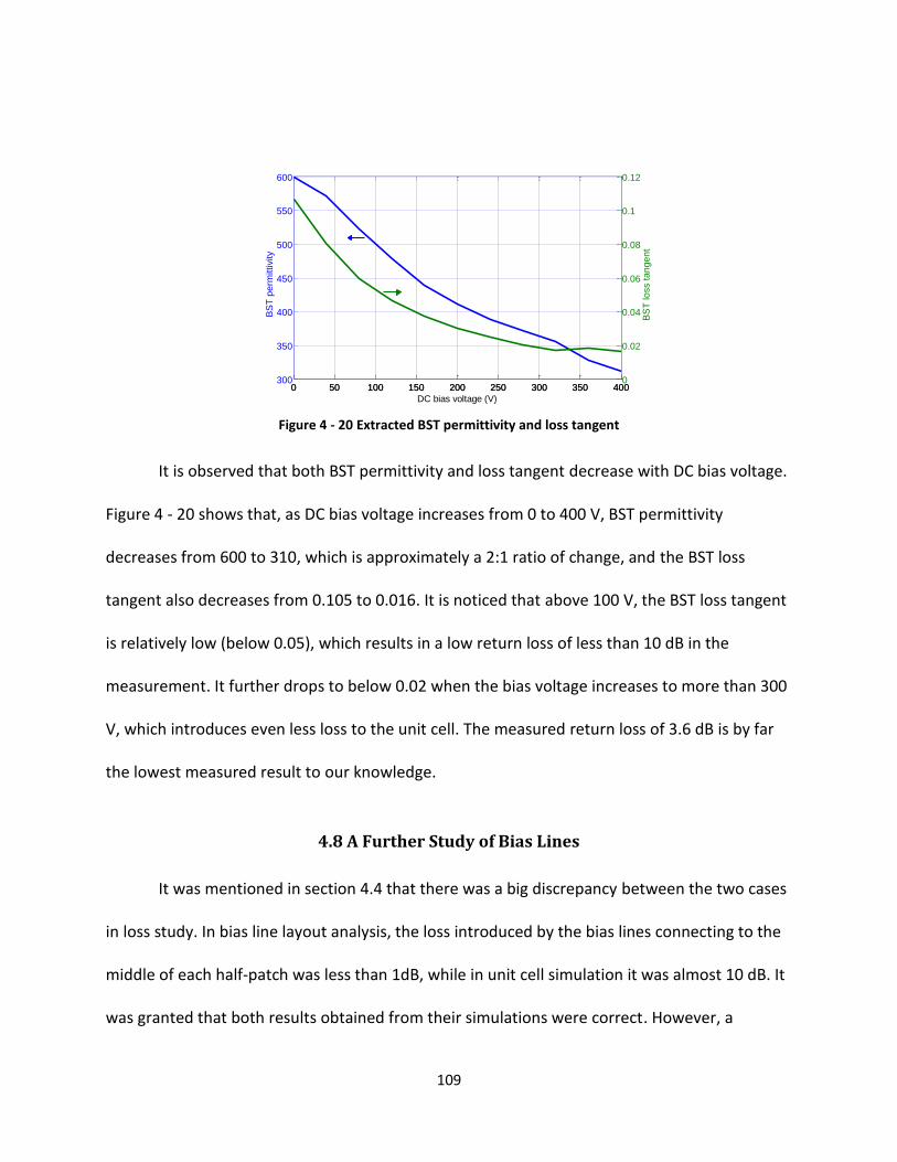
109
Figure 4 - 20 Extracted BST permittivity and loss tangent
It is observed that both BST permittivity and loss tangent decrease with DC bias voltage.
Figure 4 - 20 shows that, as DC bias voltage increases from 0 to 400 V, BST permittivity
decreases from 600 to 310, which is approximately a 2:1 ratio of change, and the BST loss
tangent also decreases from 0.105 to 0.016. It is noticed that above 100 V, the BST loss tangent
is relatively low (below 0.05), which results in a low return loss of less than 10 dB in the
measurement. It further drops to below 0.02 when the bias voltage increases to more than 300
V, which introduces even less loss to the unit cell. The measured return loss of 3.6 dB is by far
the lowest measured result to our knowledge.
4.8 A Further Study of Bias Lines
It was mentioned in section 4.4 that there was a big discrepancy between the two cases
in loss study. In bias line layout analysis, the loss introduced by the bias lines connecting to the
middle of each half-patch was less than 1dB, while in unit cell simulation it was almost 10 dB. It
was granted that both results obtained from their simulations were correct. However, a
0 50 100 150 200 250 300 350 400300
350
400
450
500
550
600
DC bias voltage (V)
BS
T p
erm
ittivity
0 50 100 150 200 250 300 350 4000
0.02
0.04
0.06
0.08
0.1
0.12
BS
T lo
ss t
an
ge
nt
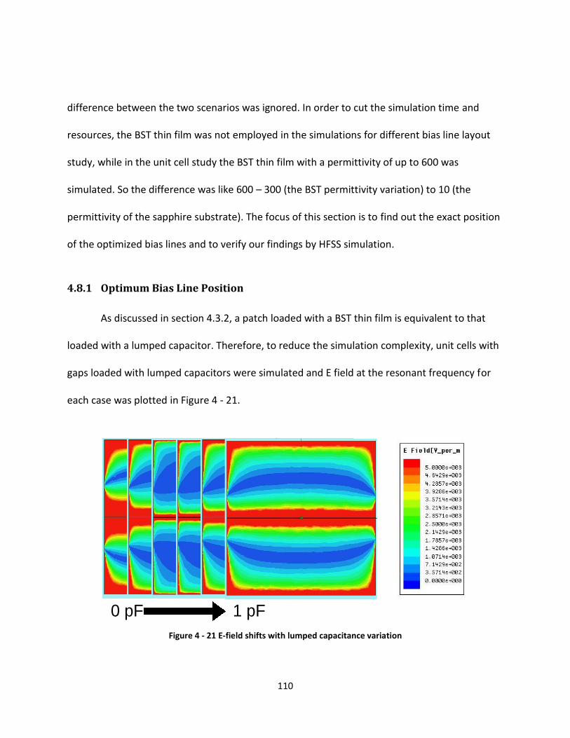
110
difference between the two scenarios was ignored. In order to cut the simulation time and
resources, the BST thin film was not employed in the simulations for different bias line layout
study, while in the unit cell study the BST thin film with a permittivity of up to 600 was
simulated. So the difference was like 600 – 300 (the BST permittivity variation) to 10 (the
permittivity of the sapphire substrate). The focus of this section is to find out the exact position
of the optimized bias lines and to verify our findings by HFSS simulation.
4.8.1 Optimum Bias Line Position
As discussed in section 4.3.2, a patch loaded with a BST thin film is equivalent to that
loaded with a lumped capacitor. Therefore, to reduce the simulation complexity, unit cells with
gaps loaded with lumped capacitors were simulated and E field at the resonant frequency for
each case was plotted in Figure 4 - 21.
Figure 4 - 21 E-field shifts with lumped capacitance variation
0 pF 1 pF
111
It is found that when the equivalent capacitance increases from 0 pF to 1 pF, the
optimum point for connecting the bias lines, the weakest location of the E-field, moves towards
the gap. The larger the BST permittivity (the bigger the lumped capacitance), the closer the
optimum point is to the gap. With all factors considered, a connection point needs to be
optimized for the case when the loss caused by the patch itself is the highest, such that the
worst loss performance of the unit cell is not going to be further worsened. As discussed in
section 4.3.2 for the patch only study, with all other conditions the same, higher BST
permittivity (equivalent to 0-V biasing) introduces higher total loss. Moreover, the BST loss
tangent is higher at lower bias voltages, as discussed in section 3.6.4. Therefore, the loss of the
unit cell without bias lines is the highest at 0-V biasing, and the optimum bias lines should be
designed for 0-V DC bias voltage. Based on the simulation results in section 4.3.2, an optimum
bias line position was found to be about 1 mm away from the gap along the side of the 6.5 mm
by 6.5 mm patch.
4.8.2 X-band Unit Cell Simulation
An HFSS simulation was performed using the optimized bias line design, and the results
are shown in Figure 4 - 22.
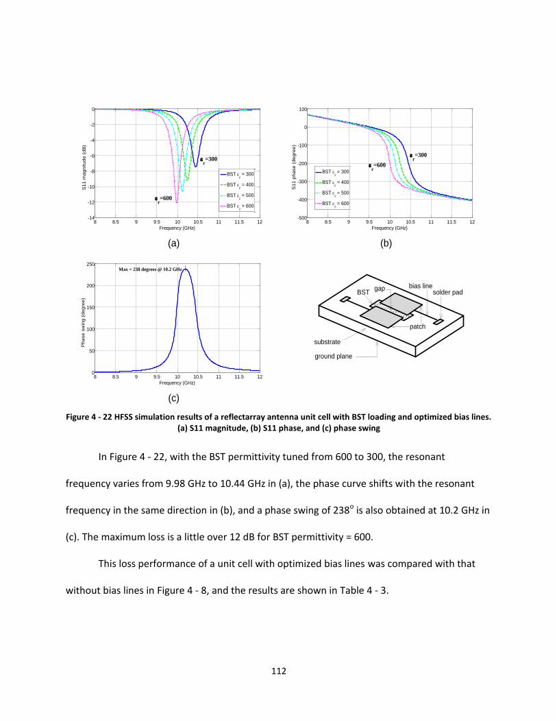
112
Figure 4 - 22 HFSS simulation results of a reflectarray antenna unit cell with BST loading and optimized bias lines. (a) S11 magnitude, (b) S11 phase, and (c) phase swing
In Figure 4 - 22, with the BST permittivity tuned from 600 to 300, the resonant
frequency varies from 9.98 GHz to 10.44 GHz in (a), the phase curve shifts with the resonant
frequency in the same direction in (b), and a phase swing of 238o is also obtained at 10.2 GHz in
(c). The maximum loss is a little over 12 dB for BST permittivity = 600.
This loss performance of a unit cell with optimized bias lines was compared with that
without bias lines in Figure 4 - 8, and the results are shown in Table 4 - 3.
(a) (b)
(c)
8 8.5 9 9.5 10 10.5 11 11.5 12-14
-12
-10
-8
-6
-4
-2
0
Frequency (GHz)
S1
1 m
ag
nitu
de
(d
B)
BST r = 300
BST r = 400
BST r = 500
BST r = 600
r=600
r=300
8 8.5 9 9.5 10 10.5 11 11.5 120
50
100
150
200
250
Frequency (GHz)
Ph
ase
sw
ing
(d
eg
ree
)
Max = 238 degrees @ 10.2 GHz
8 8.5 9 9.5 10 10.5 11 11.5 12-500
-400
-300
-200
-100
0
100
Frequency (GHz)
S1
1 p
ha
se
(d
eg
ree
)
BST r = 300
BST r = 400
BST r = 500
BST r = 600
r=300
r=600
substrate
patch
BSTgap
ground plane
solder padbias line
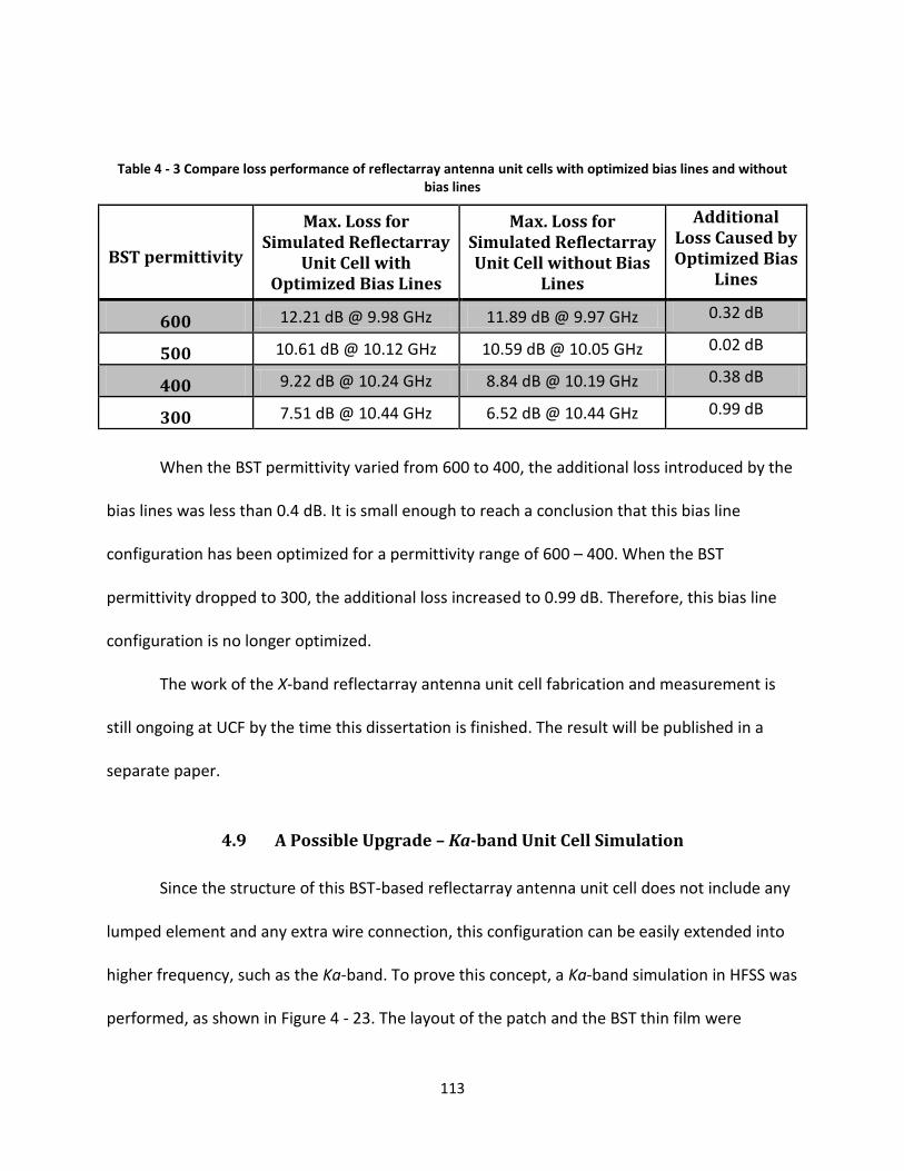
113
Table 4 - 3 Compare loss performance of reflectarray antenna unit cells with optimized bias lines and without bias lines
BST permittivity
Max. Loss for Simulated Reflectarray
Unit Cell with Optimized Bias Lines
Max. Loss for Simulated Reflectarray Unit Cell without Bias
Lines
Additional Loss Caused by Optimized Bias
Lines
600 12.21 dB @ 9.98 GHz 11.89 dB @ 9.97 GHz 0.32 dB
500 10.61 dB @ 10.12 GHz 10.59 dB @ 10.05 GHz 0.02 dB
400 9.22 dB @ 10.24 GHz 8.84 dB @ 10.19 GHz 0.38 dB
300 7.51 dB @ 10.44 GHz 6.52 dB @ 10.44 GHz 0.99 dB
When the BST permittivity varied from 600 to 400, the additional loss introduced by the
bias lines was less than 0.4 dB. It is small enough to reach a conclusion that this bias line
configuration has been optimized for a permittivity range of 600 – 400. When the BST
permittivity dropped to 300, the additional loss increased to 0.99 dB. Therefore, this bias line
configuration is no longer optimized.
The work of the X-band reflectarray antenna unit cell fabrication and measurement is
still ongoing at UCF by the time this dissertation is finished. The result will be published in a
separate paper.
4.9 A Possible Upgrade – Ka-band Unit Cell Simulation
Since the structure of this BST-based reflectarray antenna unit cell does not include any
lumped element and any extra wire connection, this configuration can be easily extended into
higher frequency, such as the Ka-band. To prove this concept, a Ka-band simulation in HFSS was
performed, as shown in Figure 4 - 23. The layout of the patch and the BST thin film were
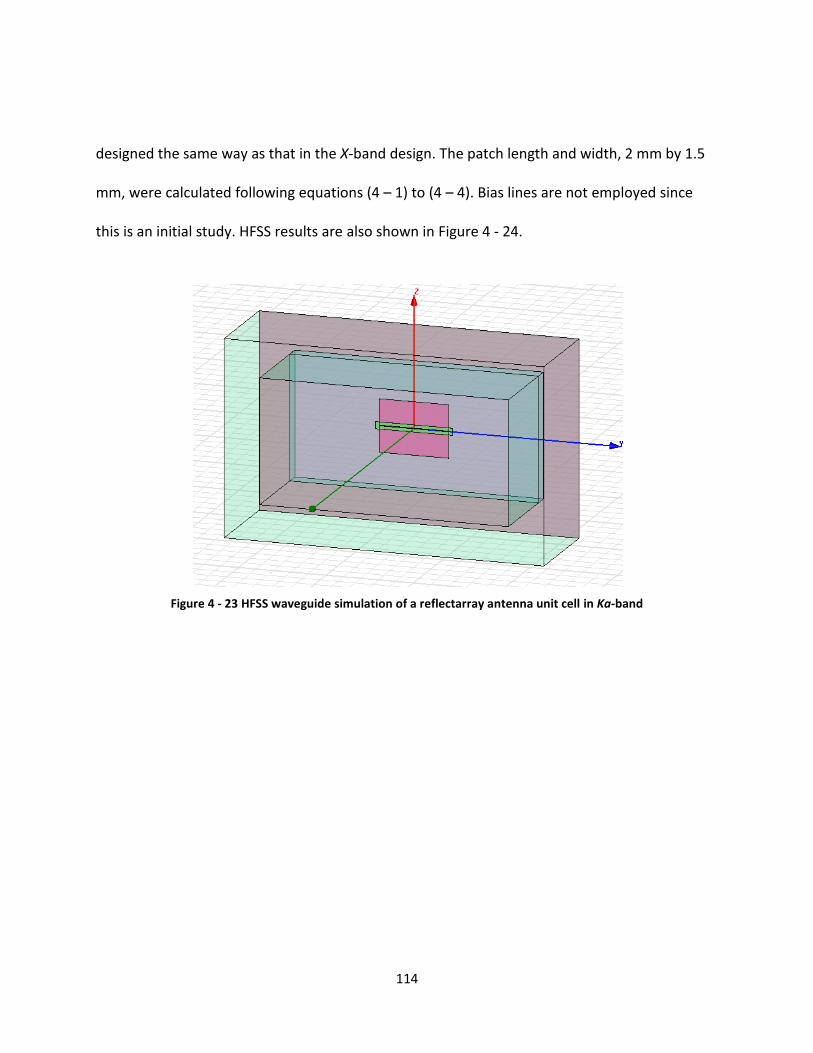
114
designed the same way as that in the X-band design. The patch length and width, 2 mm by 1.5
mm, were calculated following equations (4 – 1) to (4 – 4). Bias lines are not employed since
this is an initial study. HFSS results are also shown in Figure 4 - 24.
Figure 4 - 23 HFSS waveguide simulation of a reflectarray antenna unit cell in Ka-band
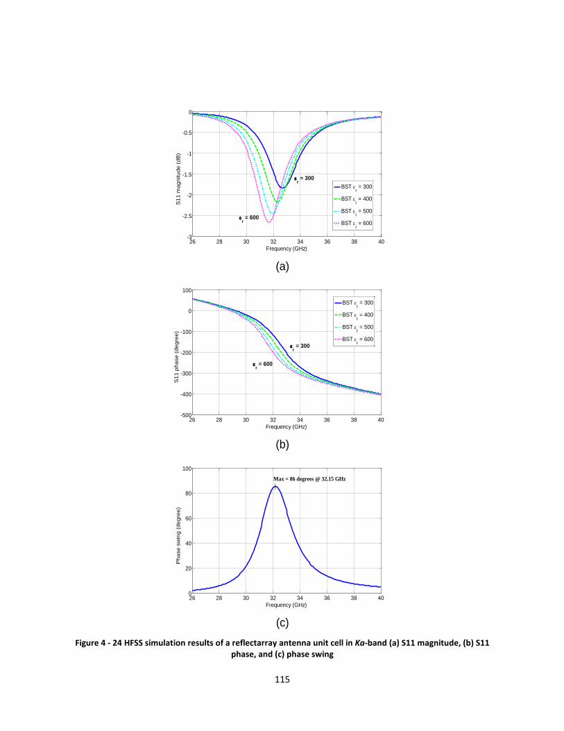
115
Figure 4 - 24 HFSS simulation results of a reflectarray antenna unit cell in Ka-band (a) S11 magnitude, (b) S11 phase, and (c) phase swing
(a)
(b)
(c)
26 28 30 32 34 36 38 40-3
-2.5
-2
-1.5
-1
-0.5
0
Frequency (GHz)
S1
1 m
ag
nitu
de
(d
B)
BST r = 300
BST r = 400
BST r = 500
BST r = 600
r = 600
r = 300
26 28 30 32 34 36 38 40-500
-400
-300
-200
-100
0
100
Frequency (GHz)
S1
1 p
ha
se
(d
eg
ree
)
BST r = 300
BST r = 400
BST r = 500
BST r = 600
r = 600
r = 300
26 28 30 32 34 36 38 400
20
40
60
80
100
Frequency (GHz)
Ph
ase
sw
ing
(d
eg
ree
)
Max = 86 degrees @ 32.15 GHz

116
With BST permittivity tuned from 600 to 300, resonant frequency varies from 31.65 GHz
to 32.7 GHz with a maximum loss of 2.66 dB. A phase swing of 86o is also obtained at 32.15
GHz. It can be concluded that this BST-loaded reflectarray antenna unit cell works very well in
Ka-band.
117
CHAPTER FIVE: CONCLUSION AND FUTURE WORK
Smart flexible electronics were studied in this dissertation.
BST material properties were first examined for its composition and crystallization. RBS
measurement showed a composition of Ba:Sr:Ti:O = 7.4:10.0:25.8:56.8, which can be
approximated to a composition of Ba0.57Sr0.43TiO3 with the excess of Ti atoms in the deposited
thin film. XRD measurement showed a strong <110> crystalline orientation.
Tunable BST IDCs were simulated, fabricated and transferred onto a flexible LCP
substrate by using a novel monolithic transfer technique. Measurement was performed from 10
MHz to 50 GHz on a Cascade probe station, and 2-prot S-parameters were obtained. Post data
analysis showed a tunability of more than 22% for the entire measured frequency range.
Lumped element values, Cs, Rs, Cp and Gp, for the equivalent circuit were calculated from Y-
parameters, which were converted from the S-parameters. Capacitance from 0.07 to 0.135 was
measured at different DC bias voltages from 0 to 200 V, and Q factors of better than 24 at 10
GHz and better than 10 at 30 GHz was obtained. This is the first time that such a high Q factor
has been reported from a tunable BST capacitor on a flexible LCP substrate. Simulation and
measurement showed good agreement. The comparison between the BST IDCs on an LCP
substrate and those on a sapphire substrate fabricated using the exact same recipe ensured
that this transfer process did not impair the performance of the tunable capacitors.
A reflectarray antenna unit cell was also designed, fabricated, simulated and measured
in X-band. The simulated results agreed very well with the measured ones. A loss as low as 3.6
118
dB was achieved when the unit cell was bias at 400 V, which is, to our knowledge, the lowest
measured return loss for the same configuration. A maximum phase swing of 263o was
obtained at 10.15 GHz, and a bandwidth of 240 MHz for a phase shift greater than 250o was
also measured. A further study of the bias line positions showed that the optimum location
changes with the capacitive loading in the gap. For our case, the horizontal bias lines placed 1
mm away from the gap improves the overall performance to about 12 dB or less, obtained from
the simulation result.
The research presented in this dissertation is a prelude for the future work in the
tunable and flexible electronics field. Based on the BST thin film transfer technique, other
tunable devices, such as phase shifters, tunable filters, etc, may be made monolithically on the
LCP or other flexible substrates. An X-band and a Ka-band phase shifters employing BST tuning
are being fabricated on LCP substrates at UCF. The reflectarray unit cell study in this work can
also be extended to a full-size array. Using the same transfer technique, this reflectarray
antenna can be made on a flexible substrate.

119
APPENDIX A: SILICON ETCHING RATE BY KOH SOLUTION
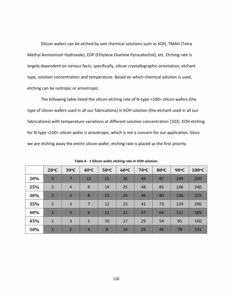
120
Silicon wafers can be etched by wet chemical solutions such as KOH, TMAH (Tetra
Methyl Ammonium Hydroxide), EDP (Ethylene Diamine Pyrocatechol), etc. Etching rate is
largely dependent on various facts, specifically, silicon crystallographic orientation, etchant
type, solution concentration and temperature. Based on which chemical solution is used,
etching can be isotropic or anisotropic.
The following table listed the silicon etching rate of N-type <100> silicon wafers (the
type of silicon wafers used in all our fabrications) in KOH solution (the etchant used in all our
fabrications) with temperature variations at different solution concentration [103]. KOH etching
for N-type <100> silicon wafer is anisotropic, which is not a concern for our application. Since
we are etching away the entire silicon wafer, etching rate is placed as the first priority.
Table A - 1 Silicon wafer etching rate in KOH solution
20oC 30oC 40oC 50oC 60oC 70oC 80oC 90oC 100oC
20% 4 7 12 15 26 49 87 149 250
25% 2 4 9 14 25 48 85 146 240
30% 2 3 8 13 24 46 80 136 225
35% 1 3 7 12 23 41 73 124 206
40% 1 3 6 11 21 37 64 111 185
45% 1 3 5 10 17 29 54 95 160
50% 1 2 4 8 14 25 46 78 131

121
APPENDIX B: CONVERSION OF S-PARAMETERS TO Y-PARAMETERS
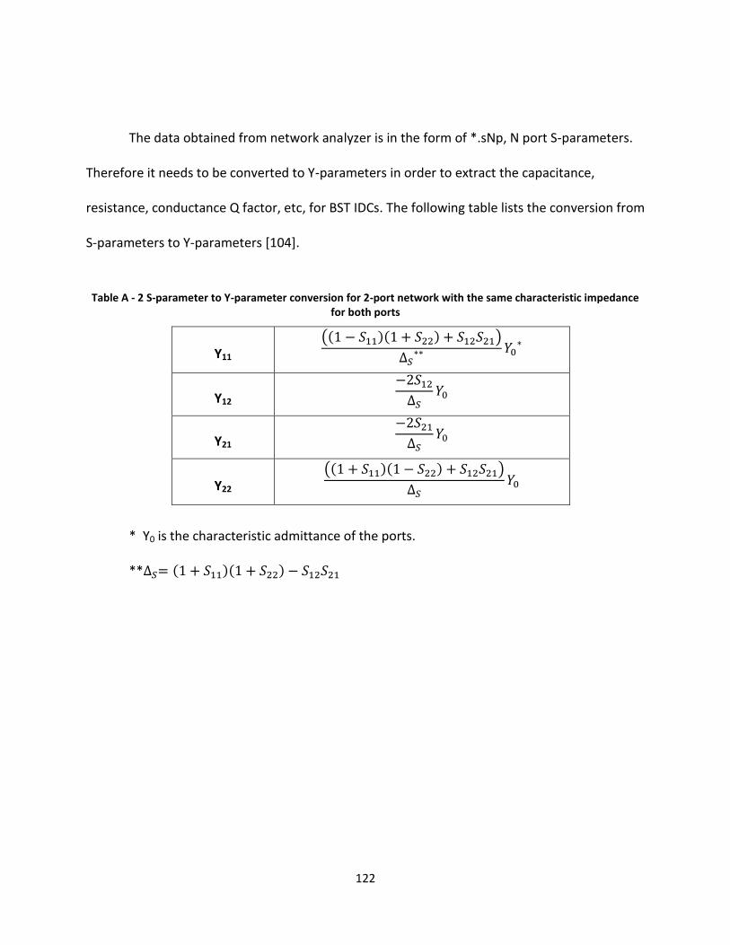
122
The data obtained from network analyzer is in the form of *.sNp, N port S-parameters.
Therefore it needs to be converted to Y-parameters in order to extract the capacitance,
resistance, conductance Q factor, etc, for BST IDCs. The following table lists the conversion from
S-parameters to Y-parameters [104].
Table A - 2 S-parameter to Y-parameter conversion for 2-port network with the same characteristic impedance for both ports
Y11
Y12
Y21
Y22
* Y0 is the characteristic admittance of the ports.
**
123
APPENDIX C: BST IDC ON LCP SUBSTRATE FABRICATION
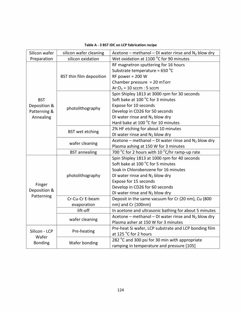
124
Table A - 3 BST IDC on LCP fabrication recipe
Silicon wafer Preparation
silicon wafer cleaning Acetone – methanol – DI water rinse and N2 blow dry
silicon oxidation Wet oxidation at 1100 oC for 90 minutes
BST Deposition & Patterning &
Annealing
BST thin film deposition
RF magnetron sputtering for 16 hours Substrate temperature = 650 oC RF power = 200 W Chamber pressure = 20 mTorr Ar:O2 = 10 sccm : 5 sccm
photolithography
Spin Shipley 1813 at 3000 rpm for 30 seconds Soft bake at 100 oC for 3 minutes Expose for 10 seconds Develop in CD26 for 50 seconds DI water rinse and N2 blow dry Hard bake at 100 oC for 10 minutes
BST wet etching 2% HF etching for about 10 minutes DI water rinse and N2 blow dry
wafer cleaning Acetone – methanol – DI water rinse and N2 blow dry Plasma ashing at 150 W for 3 minutes
BST annealing 700 oC for 2 hours with 10 oC/hr ramp-up rate
Finger Deposition &
Patterning
photolithography
Spin Shipley 1813 at 1000 rpm for 40 seconds Soft bake at 100 oC for 5 minutes Soak in Chlorobenzene for 16 minutes DI water rinse and N2 blow dry Expose for 15 seconds Develop in CD26 for 60 seconds DI water rinse and N2 blow dry
Cr-Cu-Cr E-beam evaporation
Deposit in the same vacuum for Cr (20 nm), Cu (800 nm) and Cr (100nm)
lift-off In acetone and ultrasonic bathing for about 5 minutes
wafer cleaning Acetone – methanol – DI water rinse and N2 blow dry Plasma asher at 150 W for 3 minutes
Silicon - LCP Wafer
Bonding
Pre-heating Pre-heat Si wafer, LCP substrate and LCP bonding film at 125 oC for 2 hours
Wafer bonding 282 oC and 300 psi for 30 min with appropriate ramping in temperature and pressure [105]
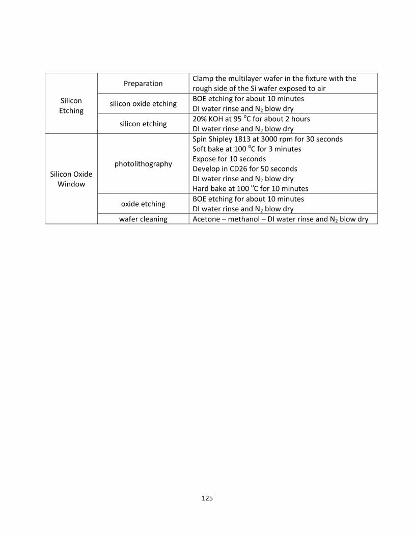
125
Silicon Etching
Preparation Clamp the multilayer wafer in the fixture with the rough side of the Si wafer exposed to air
silicon oxide etching BOE etching for about 10 minutes DI water rinse and N2 blow dry
silicon etching 20% KOH at 95 oC for about 2 hours DI water rinse and N2 blow dry
Silicon Oxide Window
photolithography
Spin Shipley 1813 at 3000 rpm for 30 seconds Soft bake at 100 oC for 3 minutes Expose for 10 seconds Develop in CD26 for 50 seconds DI water rinse and N2 blow dry Hard bake at 100 oC for 10 minutes
oxide etching BOE etching for about 10 minutes DI water rinse and N2 blow dry
wafer cleaning Acetone – methanol – DI water rinse and N2 blow dry
126
APPENDIX D: BST-BASED REFLECTARRAY ANTENNA UNIT CELL FABRICATION
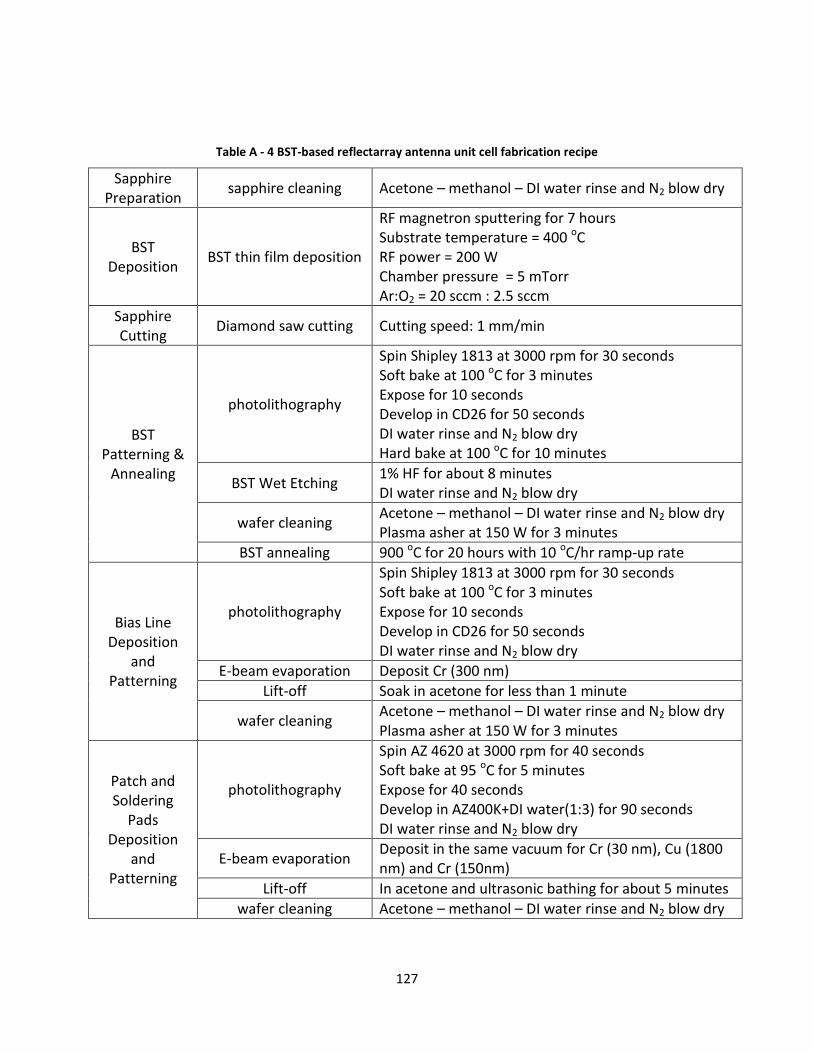
127
Table A - 4 BST-based reflectarray antenna unit cell fabrication recipe
Sapphire Preparation
sapphire cleaning Acetone – methanol – DI water rinse and N2 blow dry
BST Deposition
BST thin film deposition
RF magnetron sputtering for 7 hours Substrate temperature = 400 oC RF power = 200 W Chamber pressure = 5 mTorr Ar:O2 = 20 sccm : 2.5 sccm
Sapphire Cutting
Diamond saw cutting Cutting speed: 1 mm/min
BST Patterning &
Annealing
photolithography
Spin Shipley 1813 at 3000 rpm for 30 seconds Soft bake at 100 oC for 3 minutes Expose for 10 seconds Develop in CD26 for 50 seconds DI water rinse and N2 blow dry Hard bake at 100 oC for 10 minutes
BST Wet Etching 1% HF for about 8 minutes DI water rinse and N2 blow dry
wafer cleaning Acetone – methanol – DI water rinse and N2 blow dry Plasma asher at 150 W for 3 minutes
BST annealing 900 oC for 20 hours with 10 oC/hr ramp-up rate
Bias Line Deposition
and Patterning
photolithography
Spin Shipley 1813 at 3000 rpm for 30 seconds Soft bake at 100 oC for 3 minutes Expose for 10 seconds Develop in CD26 for 50 seconds DI water rinse and N2 blow dry
E-beam evaporation Deposit Cr (300 nm)
Lift-off Soak in acetone for less than 1 minute
wafer cleaning Acetone – methanol – DI water rinse and N2 blow dry Plasma asher at 150 W for 3 minutes
Patch and Soldering
Pads Deposition
and Patterning
photolithography
Spin AZ 4620 at 3000 rpm for 40 seconds Soft bake at 95 oC for 5 minutes Expose for 40 seconds Develop in AZ400K+DI water(1:3) for 90 seconds DI water rinse and N2 blow dry
E-beam evaporation Deposit in the same vacuum for Cr (30 nm), Cu (1800 nm) and Cr (150nm)
Lift-off In acetone and ultrasonic bathing for about 5 minutes
wafer cleaning Acetone – methanol – DI water rinse and N2 blow dry

128
Ground Plane Deposition
E-beam evaporation Deposit Cu (1000 nm)
129
LIST OF REFERENCES
[1] Eric Marsan, Jules Gauthier, Mohamed Chaker, and Ke Wu, “Tunable Microwave Device:
Status and Perspective,” in Proc. 3rd Int. IEEE NEWCAS Conf., 2005, pp. 279 - 282.
[2] Rolf Jakohy, Patrick Scheele, Stefan Muller, and Carsten Weil, “Nonlinear Dielectrics for
Tunable Microwave Components,” in Proc. 15th Int. Conf. Microw., Radar and Wireless
Commun., 2004, vol. 2, pp. 369 - 378.
[3] K.C.James Raju and K.Sudheendran, “Tunable Materials and Their Microwave
Characterization,” in Proc. Int. Conf. Microw., 2008, pp. 378 - 381.
[4] http://en.wikipedia.org/wiki/Varicap.
[5] Kenneth E. Mortenson, Variable Capacitance Diodes: The Operation and
Characterization of Varactor, Charge Storage and PIN Diodes for RF and Microwave
Applications. Dedham, MA: Artech House, 1974.
[6] Yong-Hui Shu, Julio A. Navarro, and Kai Chang, “Electronically Switchable and Tunable
Coplanar Waveguide-Slotline Band-Pass Filters,” IEEE Trans. Microw. Theory Tech., vol.
39, no. 3, pp. 548 - 554, Mar. 1991.
[7] Andrew R. Brown and Gabriel M. Rebeiz, “A Varactor-Tuned RF Filter,” IEEE Trans.
Microw. Theory Tech., vol. 48, no. 7, pp. 1157 - 1160, Jul. 2000.
[8] Sang-June Park and Gabriel M. Rebeiz, “Low-Loss Two-Pole Tunable Filters With Three
Different Predefined Bandwidth Characteristics,” IEEE Trans. Microw. Theory Tech., vol.
56, no. 5, pp. 1137 - 1148, May 2008.
130
[9] Mehmet Soyuer, Keith A. Jenkins, Joachim N. Burghartz, and Michael D. Hulvey, “A 3V
46Hz nMOS Voltage-controlled Oscillator with Integrated Resonator,” IEEE J. Solid-State
Circuits, vol. 31, no. 12, pp. 2042 - 2045, Dec. 1996.
[10] Jaewon Choi and Chulhun Seo, “Broadband and Low Phase Noise VCO Using Tunable
Metamaterial Transmission Line Based on Varactor-Loaded Split-Ring Resonator,” in
Proc. Korea-Japan Microw. Conf., 2007, pp. 145 - 148.
[11] Elliott R. Brown, “RF-MEMS Switches for Reconfigurable Integrated Circuits,” IEEE Trans.
Microw. Theory Tech., vol. 46, no. 11, pp. 1868 - 1880, Nov. 1988.
[12] S. Lucyszyn, “Review of Radio Frequency Microelectromechanical Systems Technology,”
in IEE Proc. Sci. Meas. Technol., Mar. 2004, vol. 151, no. 2, pp. 93 - 103.
[13] Tai-Ran Hsu, “Reliability In MEMS Packaging,” in Proc. IEEE 44th Annu. Int. Reliability
Physics Symp., Mar. 2006, pp. 398 - 402.
[14] Chuck Goldsmith, Tsen-Hwang Lin, Bill Powers, Wen-Rong Wu, Bill Norvell,
“Micromechanical membrane switches for microwave applications,” in Proc. IEEE MTT-S
Int. Microw. Symp. Dig., 1995, vol. 1, pp. 91 – 94.
[15] Jad Rizk, Guan-Leng Tan, Jeremy B. Muldavin, and Gabriel M. Rebeiz, “High Isolation W-
band MEMS Switches,” IEEE Microw. Wirel. Compon.Lett., Vol. 11, No. 1, pp.10 - 12, Jan.
2001.
[16] Chiao, J.-C., Fu, Y., Choudhury, D., and Lin, L-Y, “MEMS Millimeterwave Components”, in
Proc. IEEE MTT-S Int.M icrow.Symp., June. 1999, Vol. 2, pp.463–4 66.
131
[17] Robert L. Borwick, III, Philip A. Stupar, Jeffrey F. DeNatale, Robert Anderson, and Robert
Erlandson, “Variable MEMS capacitors implemented into RF filter systems,” IEEE Trans.
Microw. Theory Tech., Vol. 51, No. 1, pp. 315–319, Jan. 2003.
[18] Jung-Chih Chiao, Yiton Fu, Iao Mak Chio, Michael DeLisio and Lih-Yuan Lin, “MEMS
Reconfigurable Vee Antenna”, in Proc. IEEE MTT-S Int.Micro w. Symp., Jun. 1999, Vol. 4,
pp. 1515–1518.
[19] Chang-Wook Baek, Seunghyun Song, Jae-Hyoung Park, Sanghyo Lee, Jung-Mu Kim,
Wooyeol Choi, Changyul Cheon, Yong-Kweon Kim, and Youngwoo Kwon, “A V-band
micromachined 2-D beam-steering antenna driven by magnetic force with
polymerbasedhinges,” IEEE Trans. Microw. Theory Tech., Vol. 51, No. 1, pp. 325 - 331,
Jan. 2003.
[20] N. Scott Barker and Gabriel M. Rebeiz, “Distributed MEMS True-Time Delay Phase
Shifters and Wide-Band Switches,” IEEE Trans. Microw. Theory Tech., Vol. 46, No. 11, pp.
1881 - 1890, Nov. 1998.
[21] Juo-Jung Hung, Laurent Dussopt, and Gabriel M. Rebeiz, “Distributed 2- and 3-Bit W-
Band MEMS Phase Shifters on Glass Substrates,” IEEE Trans. Microw. Theory Tech., Vol.
52, No. 2, pp. 600 - 606, Feb. 2004.
[22] A. Malczewski, S. Eshelman, B. Pillans, J. Ehmke, and C. L. Goldsmith, “X-Band RF MEMS
Phase Shifters for Phased Array Applications,” IEEE Microw. Guid. Wave Lett., Vol. 9, No.
12, pp. 517 - 519, Dec. 1999.
132
[23] B. Pillans, S. Eshelman, A. Malczewski, J. Ehmke, and C. Goldsmith, “Ka-Band RF MEMS
Phase Shifters,” IEEE Microw. Guid. Wave Lett., Vol. 9, No. 12, pp. 520 - 522, Dec. 1999.
[24] Kamran Entesari and Gabriel M. Rebeiz, “A Differential 4-bit 6.5–10-GHz RF MEMS
Tunable Filter,” IEEE Trans. Microw. Theory Tech., Vol. 53, No. 3, pp. 1103 - 1110, Mar.
2005.
[25] Arnaud Pothier, Jean-Christophe Orlianges, Guizhen Zheng, Corinne Champeaux, Alain
Catherinot, Dominique Cros, Pierre Blondy, and John Papapolymerou, “Low-Loss 2-Bit
Tunable Bandpass Filters Using MEMS DC Contact Switches,” IEEE Trans. Microw. Theory
Tech., Vol. 53, No. 1, pp. 354 - 360, Jan. 2005.
[26] Abbas Abbaspour-Tamijani, Laurent Dussopt, and Gabriel M. Rebeiz, “Miniature and
Tunable Filters Using MEMS Capacitors,” IEEE Trans. Microw. Theory Tech., Vol. 51, No.
7, pp. 1878 - 1885, Jul. 2003.
[27] Lawrence E. Larson, “Microwave MEMS Technology for Next-generation Wireless
Communications,” in IEEE MTT-S Int. Microw. Symp. Dig., Jun. 1999, vol. 3, pp. 1073 -
1076.
[28] J Jason Yao, “RF MEMS from a Device Perspective,” J. Micromech. Microeng., vol. 10, no.
4, pp. R9 - R38, Dec. 2000.
[29] Amy C. Richards Grayson, Rebecca S. Shawgo, Audrey M. Johnson, Nolan T. Flynn,
Yawen Li, Michael J. Cima, and Robert Langer, “A BioMEMS Review: MEMS Technology
for Physiologically Integrated Devices,” Proc. IEEE, vol. 92, no. 1, pp. 6 - 21, Jan. 2004.
133
[30] Stanis Courrèges, Zhiyong Zhao, Kwang Choi, Andrew Hunt, and John Papapolymerou,
“Electronically Tunable Ferroelectric Devices for Microwave Applications,” in Microwave
and Millimeter Wave Technologies: from Photonic Bandgap Devices to Antenna and
Applications, Igor Minin, Ed. InTech, Mar. 2010, pp. 185 - 204.
[31] C. Basceri, S. K. Streiffer, A. I. Kingon, and R. Waser, “The Dielectric Response as a
Function of Temperature and Film Thickness of Fiber-textured (Ba,Sr)TiO3 Thin Films
Grown by Chemical Vapor Deposition,” J. Appl. Phys., vol. 82, no. 5, pp. 2497 - 2504,
Sep. 1997.
[32] A. K. Tagantsev, V. O. Sherman, K. F. Astafiev, J. Venkatesh, and N. Setter, “Ferroelectric
Materials for Microwave Tunable Applications,” J. Electroceramics, vol. 11, no. 1/2, pp. 5
- 66, 2003.
[33] Ali Tombak, Jon-Paul Maria, Francisco Ayguavives, Zhang Jin, Gregory T. Stauf, Angus I.
Kingon, and Amir Mortazawi, “Tunable Barium Strontium Titanate Thin Film Capacitors
for RF and Microwave Applications,” IEEE Microw. Wireless Compon. Lett., vol. 12, no. 1,
pp. 3 - 5, Jan. 2002.
[34] Jia-Shiang Fu, Xinen Alfred Zhu, Jamie D. Phillips, and Amir Mortazawi, “Improving
Linearity of Ferroelectric-Based Microwave Tunable Circuits,” IEEE Trans. Microw.
Theory Tech., vol. 55, no. 2, pp. 354 - 360, Feb. 2007.
[35] Yong-Kyu Yoon, Dongsu Kim, Mark G. Allen, and J. Stevenson Kenney, “A Reduced
Intermodulation Distortion Tunable Ferroelectric Capacitor: Architecture and
134
Demonstration,” IEEE Trans. Microw. Theory Tech., vol. 51, no. 12, pp. 2568 - 2576, Dec.
2003.
[36] Mahmoud Al Ahmad, Magali Brunet, Sandrine Payan, Dominique Michau, Mario
Maglione, and Robert Plana, “Wide-Tunable Low-Field Interdigitated Barium Strontium
Titanate Capacitors,” IEEE Microw. Wireless Compon. Lett., vol. 17, no. 11, pp. 769 - 771,
Nov. 2007.
[37] Ali Tombak, Jon-Paul Maria, Francisco T. Ayguavives, Zhang Jin, Gregory T. Stauf, Angus
I. Kingon, and Amir Mortazawi, “Voltage-Controlled RF Filters Employing Thin-Film
Barium–Strontium–Titanate Tunable Capacitors,” IEEE Trans. Microw. Theory Tech., vol.
51, no. 2, pp. 462 - 467, Feb. 2003.
[38] Jayesh Nath, Dipankar Ghosh, Jon-Paul Maria, Angus I. Kingon, Wael Fathelbab, Paul D.
Franzon, and Michael B. Steer, “An Electronically Tunable Microstrip Bandpass Filter
Using Thin-Film Barium–Strontium–Titanate (BST) Varactors,” IEEE Trans. Microw.
Theory Tech., vol. 53, no. 9, pp. 2707 - 2712, Sep. 2005.
[39] John Papapolymerou, Cesar Lugo, Zhiyong Zhao, Xiaoyan Wang, and Andrew Hunt, “A
Miniature Low-Loss Slow-Wave Tunable Ferroelectric BandPass Filter From 11- 14 GHz,”
in Proc. IEEE MTT-S Int. Microw. Symp. Dig., 2006, pp. 556 - 559.
[40] Stanis Courrèges, Yuan Li, Zhiyong Zhao, Kwang Choi, Andrew Hunt, Stephen Horst, John
D. Cressler, and John Papapolymerou, “A Ka-Band Electronically Tunable Ferroelectric
Filter,” IEEE Microw. Wireless Compon. Lett., vol. 19, no. 6, pp. 356 - 358, Jun. 2009.
135
[41] Zhiyong Zhao, Xiaoyan Wang, Kwang Choi, Cesar Lugo, and Andrew T. Hunt,
“Ferroelectric Phase Shifters at 20 and 30 GHz,” IEEE Trans. Microw. Theory Tech., vol.
55, no. 2, pp. 430 - 437, Feb. 2007.
[42] Dongsu Kim, Yoonsu Choi, Mark G. Allen, J. Stevenson Kenney, and David Kiesling, “A
Wide-Band Reflection-Type Phase Shifter at S-Band Using BST Coated Substrate,” IEEE
Trans. Microw. Theory Tech., vol. 50, no. 12, pp. 2903 - 2909, Dec. 2002.
[43] Mohsen Sazegar, Yuliang Zheng, Holger Maune, Christian Damm, Xianghui Zhou, and
Rolf Jakoby, “Compact Tunable Phase Shifters on Screen-Printed BST for Balanced
Phased Arrays,” IEEE Trans. Microw. Theory Tech., vol. 59, no. 12, pp. 3331 - 3337, Dec.
2011
[44] Gabriel Vélu, Karine Blary, Ludovic Burgnies, Aurélien Marteau, Grégory Houzet, Didier
Lippens, and Jean-Claude Carru, “A 360 BST Phase Shifter With Moderate Bias Voltage at
30 GHz,” IEEE Trans. Microw. Theory Tech., vol. 55, no. 2, pp. 438 - 444, Feb. 2007.
[45] G.Velu, K. Blary, L. Burgnies, J. C. Carru, E. Delos, A. Marteau, and D. Lippens, “A 310
/3.6-dB K-band Phaseshifter using Paraelectric BST Thin Films,” IEEE Microw. Wireless
Compon. Lett., vol. 16, no. 2, pp. 87 - 89, Feb. 2006.
[46] R. York, A. Nagra, E. Erker, T. Taylor, P. Periaswamy, J. Speck, S. Streiffer, and O. Auciello,
“Microwave Integrated Circuits using Thin-Film BST,” in Proc. 12th IEEE Int. Symp.
Applications of Ferroelectrics (ISAF), 2000, vol. 1, pp. 195 - 200.
[47] William S. Wong and Alberto Salleo, Flexible Electronics: materials and applications, New
York: Springer, 2009.
136
[48] Massimo Marrazzo (2011). A Foldable World [Online]. Available:
http://issuu.com/massimomarrazzo/docs/foldable_world.
[49] Dirk Zielke, Arved C. Hübler, Ulrich Hahn, Nicole Brandt, Matthias Bartzsch,Uta
Fügmann, Thomas Fischer, Janos Veres, and Simon Ogier, “Polymer-based organic field-
effect transistor using offset printedsource/drain structures”, Appl. Phys. Lett. vol. 87,
no. 12, pp. 123508, Sep. 2005.
[50] Sanghyun Ju, Antonio Facchetti, Yi Xuan, Jun Liu, Fumiaki Ishikawa, Peide Ye, Chongwu
Zhou, Tobin J. Marks, and David B. Janes, “Fabrication of fully transparent nanowire
transistors for transparent and flexible electronics”, Nature Nanotechnology, vol. 2, no.
6, pp. 378 – 384, Jun, 2007.
[51] Dale K. Kotter, Steven D. Novack, W. Dennis Slafer, and Patrick Pinhero, “Solar Nantenna
Electromagnetic Collectors”, in Proc. ES2008, Aug. 2008, vol. 2, no. ES2008-54016, pp.
409 - 415.
[52] Sony Corp. [Online]. Available: http://www.sony.net/SonyInfo/News/Press/201005/10-
070E/.
[53] Rak-Hwan Kim, Dae-Hyeong Kim, Jianliang Xiao, Bong Hoon Kim, Sang-Il Park, Bruce
Panilaitis, Roozbeh Ghaffari, Jimin Yao, Ming Li, Zhuangjian Liu, Viktor Malyarchuk, Dae
Gon Kim, An-Phong Le, Ralph G. Nuzzo, David L. Kaplan, Fiorenzo G. Omenetto,
Yonggang Huang, Zhan Kang, and John A. Rogers, “Waterproof AlInGaP optoelectronics
on stretchable substrates with applications in biomedicine and robotics”, Nature
Materials, vol. 9, no. 11, pp. 929–937, Oct. 2010.
137
[54] Liangbing Hu, Hui Wu, Fabio La Mantia, Yuan Yang, and Yi Cui, “Thin, Flexible Secondary
Li-Ion Paper Batteries”, ACS Nano, vol. 4, no. 10, pp. 5843–5848, Oct. 2010.
[55] Minhun Jung, Jaeyoung Kim, Jinsoo Noh, Namsoo Lim, Chaemin Lim, Gwangyong Lee,
Junseok Kim, Hwiwon Kang, Kyunghwan Jung, Leonard, A.D., Tour, J.M., and Gyoujin
Cho, “All-Printed and Roll-to-Roll-Printable 13.56-MHz-Operated 1-bit RF Tag on Plastic
Foils”, IEEE Trans. Electron Devices, vol. 57, no. 3, pp. 571 - 580, Mar, 2010.
[56] Dane C. Thompson, Manos M. Tentzeris, and John Papapolymerou, “Experimental
Analysis of the Water Absorption Effects on RF/mm-Wave Active/Passive Circuits
Packaged in Multilayer Organic Substrates,” IEEE Trans. Advanced Packaging, vol. 30,
no. 3, pp. 551 - 557, Aug. 2007.
[57] K. Jayaraj, Thomas E. Noll, and Donald R. Singh, “A Low Cost Multichip Packaging
Technology for Monolithic Microwave Integrated Circuits,” IEEE Trans. Antennas
Propag., vol. 43, no. 9, pp. 992 - 997, Sep. 1995.
[58] Dane Thompson, Nickolas Kingsley, Guoan Wang, John Papapolymerou, and Manos M.
Tentzeris, “RF Characteristics of Thin Film Liquid Crystal Polymer (LCP) Packages for RF
MEMS and MMIC Integration,” in Proc. IEEE MTT-S Int. Microw. Symp. Dig., 2005, pp.
857 - 860.
[59] Ki Seok Yang, Stephane Pinel, Il Kwon Kim, and Joy Laskar, “Low-Loss Integrated-
Waveguide Passive Circuits Using Liquid-Crystal Polymer System-on-Package (SOP)
Technology for Millimeter-Wave Applications,” IEEE Trans. Microw. Theory Tech., vol.
54, no. 12, pp. 4572 - 4579, Dec. 2006.
138
[60] Rushi Vyas, Amin Rida, Swapan Bhattacharya, and Manos M. Tentzeris, “Liquid Crystal
Polymer (LCP): The Ultimate Solution for Low-Cost RF Flexible Electronics and
Antennas,” in Proc. IEEE Antennas Propag. Society Int. Symp., 2007, pp. 1729 - 1732.
[61] G. DeJean, R. Bairavasubramanian, D. Thompson, G. E. Ponchak, M. M. Tentzeris, and J.
Papapolymerou, “Liquid Crystal Polymer (LCP): A New Organic Material for the
Development of Multilayer Dual-Frequency/Dual-Polarization Flexible Antenna Arrays,”
IEEE Antennas Wireless Propag. Lett., vol. 4, pp. 22 - 26, 2005.
[62] Sumanth Kumar Pavuluri, Changhai Wang, and Alan J. Sangster, “High
EfficiencyWideband Aperture-Coupled Stacked Patch Antennas Assembled Using
Millimeter Thick Micromachined Polymer Structures,” IEEE Trans. Antennas Propag., vol.
58, no. 11, pp. 3616 - 3621, Nov. 2010.
[63] Negar Tavassolian, Symeon Nikolaou, and Manos M. Tentzeris, “A Flexible UWB Elliptical
Slot Antenna with a Tuning Uneven U-shape Stub on LCP for Microwave Tumor
Detection,” in Proc. Asia-Pacific Microw. Conf., 2007. pp. 1 - 4.
[64] A. C. Chen, A. Pham, and R. E. Leoni, “A 6-18 GHz Push-Pull Power Amplifier with
Wideband Even-Order Distortion Cancellation in LCP Module,” in Proc. IEEE MTT-S Int.
Microw. Symp. Dig., 2007, pp. 1079 - 1082.
[65] Benjamin Lacroix, Stanis Courreges, Kwang Choi, Yongqiang Wang, Andrew T. Hunt, and
John Papapolymerou, “A Low-Loss and Compact Size Analog Tunable Filter on Flexible
Organic Substrate,” in Proc. Asia-Pacific Microw. Conf., 2010, pp. 155 - 158.
139
[66] Hao-Chih Yuan, Michelle M. Kelly (Roberts), Donald E. Savage, Max G. Lagally, George K.
Celler, and Zhenqiang Ma, “Thermally Processed High-Mobility MOS Thin-Film
Transistors on Transferable Single-Crystal Elastically Strain-Sharing Si/SiGe/Si
Nanomembranes,” IEEE Trans. Electron Devices, vol. 55, no. 3, pp. 810 - 815, Mar. 2008.
[67] Hao-Chih Yuan, Zhenqiang Ma, and George K. Celler, “Flexible RF/Microwave Switch-PIN
Diodes Using Single-Crystal Si-Nanomembranes,” in Proc. IEEE MTT-S Int. Microw. Symp.
Dig., 2007, pp. 1027 - 1030.
[68] Nickolas Kingsley, George E. Ponchak, and John Papapolymerou, “Reconfigurable RF
MEMS Phased Array Antenna Integrated Within a Liquid Crystal Polymer (LCP) System-
on-Package,” IEEE Trans. Antennas Propag., vol. 56, no. 1, pp. 108 - 118, Jan. 2008.
[69] Gordon M. Coutts, Raafat R. Mansour, and Sujeet K. Chaudhuri,
“Microelectromechanical Systems Tunable Frequency-Selective Surfaces and
Electromagnetic-Bandgap Structures on Rigid-Flex Substrates,” IEEE Trans. Microw.
Theory Tech., vol. 56, no. 7, pp. 1737 - 1746, Jul. 2008.
[70] XuefengWang, Jonathan Engel, and Chang Liu, “Liquid crystal polymer (LCP) for MEMS:
Processes and Applications,” J. Micromech. Microeng., vol. 13, no. 5, pp. 628 - 633, May.
2003.
[71] Brian Laughlin, Jon Ihlefeld, and Jon-Paul Maria, “Preparation of Sputtered (BaxSr1-x)TiO3
Thin Films Directly on Copper,” J. Am. Ceram. Soc., vol. 88, no. 9, pp. 2652 - 2654, Sep.
2005.
140
[72] Yanhua Fan, Shuhui Yu, Rong Sun, Lei Li, Mian Huang, Yansheng Yin, and Lixi Wan,
“Microstructure and Properties of Barium Strontium Titanate Thin Films Prepared on
Copper Foils via Addition of PEG to the Sol Precursor,” in Proc. Int. Conf. Electronic
Packaging Technology High Density Packaging (ICEPT-HDP 2008), 2008, pp. 1 - 4.
[73] J. Andrew Yeh, C. Alex Chang, Chih-Cheng Cheng, Jing-Yi Huang, and Shawn S. H. Hsu,
“Microwave Characteristics of Liquid-Crystal Tunable Capacitors,” IEEE Electron Device
Lett., vol. 26, no. 7, pp. 451 - 453, Jul. 2005.
[74] Kenji Uchino, Ferroelectric Devices, New York, NY: Marcel Deker, 2000.
[75] http://en.wikipedia.org/wiki/Ferroelectricity.
[76] Thomas Remmel, Richard Gregory, and Beth Baumert, “Characterization of Barium
Strontium Titanate Films Using XRD,” in Proc. Denver X-ray Conf., 1997, vol. 41, pp 38 -
45.
[77] T. M. Shaw, Z. Suo, M. Huang, E. Liniger, R. B. Laibowitz, and J. D. Baniecki, “The Effect of
Stress on the Dielectric Properties of Barium Strontium Titanate Thin Films,” Appl. Phys.
Lett., vol. 75, no.14, pp. 2129 - 2131, Oct. 1999.
[78] C. Basceri, S. K. Streiffer, A. I. Kingon, and R. Waser, “The Dielectric Response as a
Function of Temperature and Film Thickness of Fiber-textured (Ba,Sr)TiO3 Thin Films
Grown by Chemical Vapor Deposition,” J. Appl. Phys., vol. 82, no. 5, pp. 2497 - 2504,
1997.
141
[79] J. D. Baniecki, R. B. Laibowitz, T. M. Shaw, P. R. Duncombe, D. A. Neumayer, D. E.
Kotecki, H. Shen, and Q. Y. Ma, “Dielectric Relaxation of Ba0.7Sr0.3TiO3 Thin Films from
1 MHz to 20 GHz,” Appl. Phys. Lett., vol. 72, no. 4, pp. 498-500, 1998.
[80] P. Padmini, T. R. Taylor, M. J. Lefevre, A. S. Nagra, R. A. York, and J. S. Speck, “Realization
of High Tunability Barium Strontium Titanate Thin Films by RF Magnetron Sputtering,”
Appl. Phys. Lett., vol. 75, no. 20, pp. 3186 - 3188, 1999.
[81] Ming Shiahn Tsai, S. C. Sun, and Tseung-Yuen Tseng, “Effect of Bottom Electrode
Materials on the Electrical and Reliability Characteristics of (Ba,Sr)TiO3 Capacitors,” IEEE
Trans. Electron Devices, vol. 46 , no. 9, pp. 1829 - 1838, 1999.
[82] http://www.ajaint.com/whatis.htm.
[83] Robert Eason, Pulsed Laser Deposition of Thin Films, Hoboken, NJ: Wiley, 2007.
[84] Ki-Byoung Kim, Tae-Soon Yun, Jong-Chul Lee, Hyun-Suk Kim, Ho-Gi Kim, and Il-Doo Kim,
“Integration of Coplanar (Ba,Sr)TiO3 Microwave Phase Shifters onto Si Wafers Using
TiO2 Buffer Layers,” IEEE Trans. Ultrasonics Ferroelectrics Frequency Control, vol. 53, no.
3, pp. 519 - 524, Mar. 2006.
[85] Larry L. Hench and Jon K. West, “The sol-gel process,” Chem. Rev., vol. 90, no. 1, pp 33 -
72, 1990.
[86] G. Vélu, J. C. Carru, E. Cattan, D. Remiens, X. Mélique, and D. Lippens, “Deposition of
Ferroelectric BST Thin Films by Sol-gel Route in View of Electronic Applications,”
Ferroelectrics, vol. 288, pp. 59 - 69, 2003.
142
[87] Richard C. Jaeger, "Film Deposition," in Introduction to Microelectronic Fabrication,
Upper Saddle River, NJ: Prentice Hall, 2002.
[88] C. Basceri, S. K. Streiffer, A. I. Kingon, and R. Waser, “The Ddielectric Response as a
Function of Temperature and Film Thickness of Fiber-textured (Ba,Sr)TiO3 Thin Films
Grown by Chemical Vapor Deposition,” J. Appl. Phys., vol. 82, no. 5, pp. 2497 - 2504,
1997.
[89] G. Wang, T. Polley, A. Hunt, and J. Papapolymerou, “A High Performance Tunable RF
MEMS Switch Using Barium Strontium Titanate (BST) Dielectrics for Reconfigurable
Antennas and Phased Arrays,” IEEE Antennas Wireless Propag. Lett., vol. 4, pp. 217 -
220, 2005.
[90] Ya Shen, Siamak Ebadi, Parveen Wahid, and Xun Gong, “Tunable and Flexible Barium
Strontium Titanate (BST) Varactors on Liquid Crystal Polymer (LCP) Substrates,” in Proc.
IEEE MTT-S Int. Microw. Symp. Dig., 2012, to be published.
[91] http://www.cleanroom.byu.edu/KOH.phtml.
[92] Inder Bahl, Lumped Elements for RF and Microwave Circuits. Norwood, MA: Artech
House, 2003.
[93] J. Zhang, M. W. Cole, and S. P. Alpay, "Pyroelectric properties of barium strontium
titanate films: Effect of thermal stresses," J. Appl. Phys., vol. 108, no 5, pp. 054103 –
054103-7, 2010.
143
[94] B. Su, T. W. Button, T. Price, D. Iddles, and D. Cannell, "Dielectric properties of barium
strontium titanate (BST)/yttrium aluminate (YAlO3) thick films under DC bias field", J.
Mater. Sci., vol 43, no. 3, pp. 847 - 851, 2008.
[95] J. Park, J. Lut, S. Stemmert, and R. York, "Microwave Planar Capacitors Employing Low
Loss, High-K, and Tunable BZN Thin Films," IEEE MTT-S Int. Microw. Symp. Dig., June
2005, pp. 607 - 610.
[96] John Huang, José A. Encinar, Reflectarray antennas. Hoboken, NJ: Wiley, 2008, pp. 1-6.
[97] S. V. Hum, M. Okoniewski, and R. J. Davies, “Modeling and design of electronically
tunable reflectarrays,” IEEE Trans. Antennas Propag., vol. 55, no. 8, pp. 2200–2210, Aug.
2007.
[98] L. Boccia, G. Amendola, and G. D. Massa, “Performance Improvement for a Varactor-
Loaded Reflectarray Element,” IEEE Trans. Antennas Propag., vol. 58, no. 2, pp. 585–
589, Feb. 2010.
[99] H. Rajagopalan, Y. Rahmat-Samii, and W. A. Imbriale, “RF MEMS actuated reconfigurable
reflectarray patch-slot element,” IEEE Trans. Antennas Propagat., vol. 56, no. 12, pp.
3689-3699, Dec 2008.
[100] Y. Shen, S. Ebadi, P. Wahid, and X. Gong, Tunable Reflectarray Unit Cell Element Using
BST Technology, presented at the 2012 IEEE Radio and Wireless Symposium, Santa
Clara, CA, Jan. 15 - 19 2012.
144
[101] M. Sazegar, A. Giere, Z. Yuliang, H. Maune, A. Moessinger, R. Jakoby, “Reconfigurable
Unit Cell for Reflectarray Antenna Based on Barium-Strontium-Titanate Thick-Film
Ceramic” In Proc. of European microwave conference 2009, pp. 598-601, Sept-Oct. 2009.
[102] Constantine A. Balanis, Antenna Theory: Analysis and Design, 3rd ed. Hoboken, NJ: Wiley,
2005.
[103] http://www.cleanroom.byu.edu/KOH.phtml.
[104] David M. Pozar, Microwave Engineering, 4th ed. Hoboken, NJ: Wiley, 2011
[105] ULTRALAM 3000 Series Liquid Crystalline Polymer Circuit Materials Fabrication
Guidelines [Online]. Available: http://www.rogerscorp.com.