Embed Size (px)
Citation preview
University of Bath
PHD
An investigation of the microwave properties of resonant tunnelling devices
Sammut, Carmel Victor
Award date:1992
Awarding institution:University of Bath
Link to publication
Alternative formatsIf you require this document in an alternative format, please contact:[email protected]
Copyright of this thesis rests with the author. Access is subject to the above licence, if given. If no licence is specified above,original content in this thesis is licensed under the terms of the Creative Commons Attribution-NonCommercial 4.0International (CC BY-NC-ND 4.0) Licence (https://creativecommons.org/licenses/by-nc-nd/4.0/). Any third-party copyrightmaterial present remains the property of its respective owner(s) and is licensed under its existing terms.
Take down policyIf you consider content within Bath's Research Portal to be in breach of UK law, please contact: [email protected] with the details.Your claim will be investigated and, where appropriate, the item will be removed from public view as soon as possible.
Download date: 30. Mar. 2022
AN INVESTIGATION OF THE MICROWAVE PROPERTIES OF RESONANT TUNNELLING DEVICES
Submitted by C a m e l Victor Sammut for the degree of PhD
of the University of Bath 1992
COPYRIGHT
Attention is drawn to the fact that copyright of this thesis rests with its author. This copy of the thesis has been supplied on condition that anyone who consults it is understood to recognize that its copyright rests with the author and that no quotation from the thesis and no information derived from it may be published without the prior written consent of the author.

UMI Number: U548879
All rights reserved
INFORMATION TO ALL USERS The quality of this reproduction is dependent upon the quality of the copy submitted.
In the unlikely event that the author did not send a complete manuscript and there are missing pages, these will be noted. Also, if material had to be removed,
a note will indicate the deletion.
Dissertation Publishing
UMI U548879Published by ProQuest LLC 2013. Copyright in the Dissertation held by the Author.
Microform Edition © ProQuest LLC.All rights reserved. This work is protected against
unauthorized copying under Title 17, United States Code.
ProQuest LLC 789 East Eisenhower Parkway
P.O. Box 1346 Ann Arbor, Ml 48106-1346

UNIVERSITY OF BATH LIBRARY
[24. I 19 FEB 1993"Ph rv _
f O { ’ I f.f }

To my wife Mary Hose and sons
Neil and Keith.
They have endured so much for the sake of Science!
ABSTRACT
This thesis presents a study of the microwave properties of resonant tunnelling devices.
Low frequency stability is considered as this affects device applicability potential. It is shown that bias circuit instabilities can be simulated assuming a simplified model and that the simulated effects can account for observed features in the dc current-voltage characteristics.
Small-signal reflection measurements between 45 MHz and 13 GHz were performed. The experimental results, the most accurate published to date, fitted to within less than 5% difference from those simulated using a tunnel diode equivalent circuit model with frequency-independent parameters and voltage-dependent conductance and capacitance. These measurements allowed the device capacitance to be determined over a wide voltage range. This was made possible by the use of a hitherto un-characterised microwave package and accurate de-embedding techniques based on the derivation of a lumped-element equivalent circuit for the package inside a novel 3.5 mm coaxial mount which was designed and constructed for the purpose.
Large-signal impedance measurements were also performed. The results fitted the tunnel diode model with frequency-independent parameters over narrow frequency bands.
The large-signal behaviour of resonant tunnelling devices was investigated numerically using a computer program modified to employ the experimental small-signal model as a starting point. A simple multiplier circuit was used to compare experimental results with calculations. The comparison shows that accurate large-signal analysis is possible with this technique.
ii
Table of Contents
CHAPTER 1: Resonant Tunnelling Devices 11.1 Introduction 11.2 The Basic Physics of ResonantTunnelling 51.2.1 The Tunnelling Current 51.2.2 The Tunnelling Probability 81.2.2.1 The Transfer-Matrix Method 9
1.3 Resonant Tunnelling versus Sequential Tunnelling 131.4 Equivalent Circuit Models 17References 24
CHAPTER 2: Dc Characterisation andBias Circuit Instability 302.1 Introduction 302.2 The tested devices 312.2.1 The MBE devices 312.2.2 The MOCVD devices 382.3 Bistability and Hysteresis in theI-V characteristic 412.3.1 Stability criteria 472.3.2 Observation and Simulation of bias circuit oscillations andextrinsic bistability 542.3.2.1 Time-domain behaviour 572.3.2.2 Simulation of unstable I-Vcharacteristics 65
2.4 Implications of dc stability criteria on rf power generation 69References 70
CHAPTER 3: De-embedding Techniques 753.1 Introduction 753.2 De-embedding devices 763.2.1 Lumped-element equivalent circuit synthesis 783.2.1.1 Package equivalent circuit 81
iii
3.2.2 Two-port network representationof package and mount discontinuities 843.2.2.1 Basic technique 86
3.3 The S4-type package mount 913.4 The E10/A microwave package 933.4.1 The 3.5mm backshort mount 943.4.2 Package-mount equivalent circuit 953.4.3 Determination of the lumpedequivalent circuit elements 973.4.3.1 Measurements on the emptypackages 973.4.3.2 Measurements on the dummysolid package 993.4.3.3 Measurements on the dummyopen-circuited package 1003.4.3.4 Measurements on the dummyshort-circuited package 1043.4.3.5 Calculated estimates of thepackage parameters 1073.4.4 Summary of results 109
References 110
CHAPTER 4: Small- and Large-signalDevice Equivalent Circuit Models 1134.1 Introduction 1134.1.1 Small- and large-signal admittance 1134.2 Small-signal measurements 1144.2.1 Small-signal equivalent circuitmodel of the RTD 523B 1154.2.1.1 Experimental procedure 1174.2.1.2 Results and analysis 1184.2.1.3 Simulation of experimentalresults 1234.2.1.4 Effects of test-signal power 130
4.3 Large-signal Measurements 1404.3.1 Large-signal impedance of theRTD GWS160 1434.3.1.1 Some important observations 1464.3.1.2 Results and Analysis 1474.3.2 Large-signal impedance of theRTD 523B 152
iv
4.3.2.1 Observations 1534.3.2.2 Results and Analysis 153
4.4 Summary of the main results andconclusions 155References 156
CHAPTER 5: Large-signal Analysis of aSimple RTD Multiplier 1595.1 Introduction 1595.2 Frequency multiplication with resonant tunnelling devices 1605.2.1 Odd harmonic multiplier 1605.2.2 Doubler 1635.3 Multiplier Analysis 1645.3.1 The multiple reflection technique 1665.3.2 Details of the large signalanalysis 1695.4 The multiplier analysis program 1745.4.1 The large signal analysis subroutine 1745.4.2 Port impedances and conversionproperties 1795.5 Experiment and analysis 1815.5.1 Measurement of the harmonic output power 1825.5.2 Experimental results and simulation for a 1 GHz pump signal 1875.5.2.1 Harmonic output power 1875.5.2.2 Conversion loss and efficiency 1955.5.2.3 Rectified current 2025.5.3 Experimental results at higherfrequencies 2075.5.3.1 Pump frequencies between 2 and6 GHz 2075.5.4 Sweeping the pump power at zerobias 2095.6 Concluding remarks 212References 213
CHAPTER 6: Concluding Notes 219
v

6.1 Introduction6.2 Summary and discussion of the main observations and conclusions6.2.1 Bias circuit oscillations6.2.2 Small- and large-signal equivalent circuits and some useful observations6.2.3 Large-signal analysis and harmonic multiplication6.3 Some recent novel designs for improving RTD oscillatorsReferences
Appendix I: Design and construction of the dc characterisation station
Appendix II: Bias circuit simulation program
Appendix III: Device processing and packaging
Appendix IV: Typical RTD oscillation spectra
Appendix V: Nonlinear analysis program
Acknowledgements
CHAPTER 1
RESONANT TUNNELLING DEVICES
1.1 Introduction
The first report of negative differential resistance (NDR) from a tunnelling structure was due to Esaki in 1958 [1]. In a tunnelling structure, NDR occurs when the total number of tunnelling electrons transmitted across a barrier structure per second decreases, rather than increases, with an increase in applied voltage. The negative resistance regions in the I-V characteristics themselves are not only important in solid-state electronics because of possible signal amplification, but also shed light on some fundamental aspects of tunnelling [2].
Since then, much has been achieved in the field of solid-state tunnelling structures, but the intention here is to focus on a particular class of semiconductor tunnelling structures which have become known as resonant tunnelling devices (RTD's). In 1969, Duke [3] predicted a new phenomenon due to quantum confinement of charge carriers. In 1973, Tsu and Esaki [4] predicted NDR in a finite superlattice as a consequence of resonant tunnelling. The first experimental results were obtained by Chang et al. [5] who demonstrated the existence of NDR regions in the I-V characteristic of a double barrier quantum well (DBQW), AlGaAs-GaAs-AlGaAs heterostructure grown by molecular beam epitaxy (MBE). Similar observations were subsequently reported [6] with an MBE-grown AlGaAs-GaAs multi-barrier quantum well (MBQW) superlattice. This epitaxial growth process was then still in its infancy. The quality of the samples grown immediately
1
after the pioneering work of Chang and Esaki [5,6] did not result in much improved non-linearity regions in the I/V characteristics. Indeed these works found effects only at low temperatures and even here, these were much less pronounced than expected from theory. This implicitly suggested the idea that resonant tunnelling was too critically dependent on experimental parameters to be really controllable and reproducible, let alone exploited, in actual samples with defect concentrations, surface cleanliness, actual dimensions, etc., different from the clear-cut pictures of theoretical models. As a result, interest in these structures dwindled for almost a decade.
Since then, however, the quality of epitaxial layers grown by MBE had improved considerably and in 1983, Sollner et al. reported a peak-to-valley current ratio (PVR) of 6 at low temperatures and claimed to have carried out successful detecting and mixing experiments at 2.5THz [7,8]. Almost a year later, the same group announced the observation of 186Hz oscillations from a DBRTD at temperatures of about 200K [9], Shewchuk et al. [10] were the first to report room temperature NDR regions in the I-V characteristics of a DBRT heterostructure based on the AlxGai_xAs-GaAs system with a PVR of 1.5 (8) at 300K (77K).
By this time, interest in resonant tunnelling structures had rekindled, as evidenced from the vast amount of relevant literature published. Immediately after the announcement by Shewchuk et al. [10] the first observation of NDR in AlAs/GaAs DBRT heterostructures grown by metalorganic chemical vapour deposition (MOCVD) was reported [11]. Published room-temperature results on GaAs-AlGaAs MOCVD- grown resonant tunnelling structures are rare and significantly inferior to those of similar MBE structures (e.g. PVR < 1.5 and J p< l k A c m ' 2 [56]). For structures in the InAlAs-InGaAs material system [57] typical PVR's are about 9 times lower than for similar MBE structures. The char
2
acteristics for GaAs-AlGaAs MOCVD-grown structures have been marginally improved to V p* 2 k A c m ' 2 and PVR's greater than 2 [58] (see chapter 2).
Until about 1985, most of the structures grown and tested had n+-type emitters and collectors; i.e., resonant tunnelling had only been demonstrated for electrons. Mendez et al. [12] were the first to report resonant tunnelling due to holes in an AlAs-GaAs-AlAs DBQW sandwiched between p+-GaAs regions.
By 1986, the PVR in the dc characteristics of AlAs-GaAs DBRT devices had risen to 3.5 at room temperature [13]. Huang et al. reported 3.9 at room temperature the following year for an Alo.42Gao.58As-GaAs DBRT heterostructure [14] . There then seemed to be a consensus that the non-linearities obtainable from the AlAs-GaAs or AlGaAs-GaAs systems could not be further improved. However, the extent of NDR and peak current densities had been improved sufficiently to enable such devices to give rise to microwave oscillation at frequencies of 56GHz (60p,l/ - fundamental) and 87GHz (18p.l/ - second harmonic) [15,16,17] when placed in microwave cavities.
Interest was by no means confined to DB structures. NDR has been reported in a single barrier - QW device [18] in which electrons tunnel through the AlAs barrier into the GaAs QW and subsequently drift to a lateral contact. Two peaks in the I-V curve at low-temperature for a triple barrier diode were observed by Nakagawa et al. [19], while Reed et al. [20] reported resonant tunnelling in a DB structure in which the barriers had been replaced by thin short period binary superlattices of AlAs and GaAs. However, the most promising results have come from structures involving In in ternary or binary alloy systems inside or outside the QW.
3
The first such structure was due to Inata et al. [21]. It consisted of an InGaAs QW sandwiched between two InAlAs barriers grown by MBE on an epitaxial layer of InGaAs lattice-matched to an InP substrate. This device gave a PVR of 2.3 at room temperature and 11.7 at 77K. The first pseudomorphic structure was reported in 1987 [22]. Itsstructure was similar to the former but had AlAs instead of InAlAs in the barriers. The improvement was dramatic. The PVR reported for this device was 14 at 300K and 35 at 77K. However, there was yet to be a further significant improvement the following year. This was due to Broekaert et al. [23] and was another pseudomorphic heterostructure, grown by MBE, having strained AlAs barriers and a QW consisting of 3 monolayers of InGaAs cladding 6 monolayers of InAs on either side. These layers were sandwiched between InGaAs undoped spacer layers and grown on epitaxial InGaAs lattice-matched to InP as the substrate. This structure gave the best PVR to date; 30 at room temperature and 63 at 77K with a peak current density of 6kAcm“2 .
The realisation that the negative resistance region in RTD characteristics is capable of providing the gain necessary for high frequency oscillations led to a series of reports of oscillations exceeding in frequency the previously reported 56GHz [15,16,17]; 200Ghz [24] and 420GHz, with a predicted maximum oscillation frequency of ITHz [25]. Various material parameters in the GaAs-AlGaAs and GaAs-AlAs material systems preclude operation at higher frequencies [25]. In this respect, the InGaAs-AlAs and similar material systems [23] were investigated in order to circumvent these problems. Other systems have been investigated, such as InAs-AlSb [59,60,61,62,63] and InSb-AlInSb [64] grown on GaAs substrates since these are more suitable for fabrication of monolithic integrated circuits. The InAs-AlSb system has proved most promising with the recent reports of 712 GHz oscillations at 0.3p.W [65] from a 1.8p.m-diameter device.
4
Three-terminal devices using resonant tunnelling in various ways have also been proposed [26] and the future of such devices seems promising, even though the relative lack of literature in this area may suggest otherwise.
Considerable effort has been made towards a better understanding of the equivalent circuit of the device [27,28,29,30,31,32] and underlying processes for the frequency response [33]. It is here that this work attempts to contribute by examining the behaviour of some resonant tunnelling devices at low and microwave frequencies. The interaction of the RTD with the bias circuit is investigated in chapter 2, which analyses in detail the nature and origin of low-frequency bias circuit oscillations. Subsequent chapters tackle small- and large-signal device behaviour at microwave frequencies. In particular, chapter 5 applies numerical self-consistent methods to investigate the behaviour of RTD's as harmonic multipliers using an experimentally-based small-signal equivalent circuit model obtained as described in chapter 4.
1.2 The basic physics of resonant tunnelling
1.2.1 The tunnelling current
Let us consider a GaAs-AlxGai_xAs single crystal with an abrupt interface between the two regions. The alloy AlxGai_xAs has a wider bandgap than GaAs with some of this difference appearing in the conduction band. It thus acts as a barrier with height, relative to the GaAs conduction band edge, of [34]
A E c = 0.65(1.247x) (1-1)
5

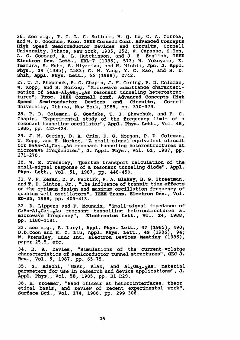
where 1.247x is the band gap difference [35] and 0.65 is the fraction appearing in the conduction band [36] (figure 1.1).
V(z)
Figure 1.1. Electronic potential energy at an interface between two materials of different band gaps. The motion of an electron in material 1 is restricted along the z-direction because of a potential barrier at the junction.
The electrons on both sides of the interface move in a screened potential due to the ion cores, while interacting with each other via the Coulomb potential. The Hamiltonian of the system is complicated and is thus frequently simplified by using one electron states that take into account the periodic component of the electron-ion potential [37,38].
Since there is no electrostatic potential parallel to the interface, only a one-dimensional Schrodinger equation need be considered. Thus, in the free-electron approximation, solutions are sought to an equation of the form
h2 d22 m d z 2+ V(z)-E
(1.2)
V(z) is the potential near the interface and is an envelopefunction which is subject to the following conditions imposed by conservation of particle flux at any interface
(1.3)
6
1 dT|>£ i dijj£ (1*4)mi dz _ m 2 dz
z 1 zx
where z\ and z\ refer to positions to the left and to theright of respectively, and and m 2 are the electron effective masses in regions 1 and 2.
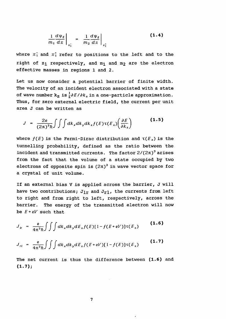
Let us now consider a potential barrier of finite width. The velocity of an incident electron associated with a state of wave number kz is l-dE/dkz in a one-particle approximation. Thus, for zero external electric field, the current per unit area J can be written as
2e r r r ( a e \ (i-s)7 " (2 n j * f t J J J d k * d k y d k
where /(F) is the Fermi-Dirac distribution and t (Fz) is the tunnelling probability, defined as the ratio between the incident and transmitted currents. The factor 2/(2n)3 arises from the fact that the volume of a state occupied by two electrons of opposite spin is (2n)3 in wave vector space for a crystal of unit volume.
If an external bias V is applied across the barrier, J will have two contributions; Jir and Jrl/ the currents from left to right and from right to left, respectively, across the barrier. The energy of the transmitted electron will now be E + eV such that
Jir “ J j dfc*dfc,d£2/(£-)[l-/(£- + e K ) ] T ( i r z ) ( 1 ' 6 )
J , ‘ " 4^fi/ 1 f d k * d k yd E z f ( .E + e m i - f ( . E ' n i ( . E z ' ) (1'7)
The net current is thus the difference between (1.6) and (1.7);
7
j _ _e r r r ____ . (i.s)4ji ftj J Jdfcxd/cyd£-i[/(£')-/(£- + eK)]x(£-J
The zero-temperature limit for the free-electron approximation gives [39]
,, 2nm (1.9)dkxdkv = — z-dEi
y n 2 1
where E ( is the electron energy component parallel to theinterface. Hence, the tunnelling current can be written as [39]
e m T fEf~*v r*r ~ \ i o v e V < E F
(1.10)
J - e m fore >£,Znzh3Jo e " *' (1-11)
Equations (1.10) and (1.11) can be evaluated provided that t(Ez) is known.
1.2.2 The tunnelling probability
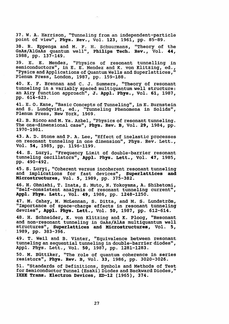
The tunnelling probability is determined by solving Schrodinger's equation. Analytical solutions can only be obtained for a few barrier profiles such as the one in figure1.2 (a). This profile can serve as a first approximation to the situation of a thin, undoped, semiconductor sandwiched between two thick layers of degenerately doped semiconductors of lower energy gap (e.g. GaAs-AlGaAs-GaAs heterostructure).
If an external voltage is applied across the doped regions, the barrier shifts as shown qualitatively in figure 1.2 (b) and will become essentially triangular when the applied voltage Vg is such that eVB> A E c (figure 1.2 (c)).
8
1 2 3
(a) (b) (c)
Figure 1.2. Rectangular potential model representing two regions of degenerately doped semiconductor with an interposed region of undoped material of higher band gap, (a) with no externally applied voltage, (b) and (c) with an external applied voltage and Vg, respectively.
In the case of the rectangular barrier, the solution of(1.2) is expressed in terms of plane waves in regions 1 and 3 (figure 1.2 (a)). In region 2, can be written as a linear combination of the Airy functions A i ( z ) and B i ( z ) [34,39,40]. By matching the wave functions and their derivatives divided by the respective effective masses in the three regions (i.e., applying the boundary conditions(1.3) and (1.4)), the relative amplitudes of the incident and transmitted waves are determined, from which x may be calculated.
1.2.2.1 The transfer-matrix method
If, for simplicity, we assume the potential V(z) to be constant in a given region, the general solution of (1.2) has the form of a linear combination of waves propagating normal to the interface;
\p£ = A e x p ( j k z ) + B e x p ( - j k z ) (1*12)
with
9

(1.13)E-V
2m
When E- V >0, k is real and the wave functions are plane waves. When E-V < 0, k is imaginary and the wave functions are exponentially growing and decaying waves. Thus the overall wave function for the potential step in figure 1.1 has a plane-wave form for z < z x (for electron energies such that E-V>0) and an exponentially decaying wave form for z > z Y (E - V <0) . The coefficients A and B in (1.12) are determined from the boundary conditions (1.3) and (1.4) for
Ai and Bi can be related to A 2 and B2 by means of a matrix M such that
Now, for the general case of n regions (figure 1.3) with corresponding potentials Vi and effective masses mi (i = 1, 2, ..., n), separated by rc-1 interfaces at positions zi (i = 1,2, ...,n), the wave functions at the extreme left hand region 1 and the extreme right hand region n are linked by
z = zi
>4,expCy'/Cj2Tj) + fij expC-yfcjZj) = /42exp(yfc2zi) + 2exP("7fc2zi) (1.14)
{A lexp(jklz l')-Blexp(-jkiz i)> {A 2exp(jk2z l)-B2exp(-jk2z i)> (1.15)
(1.16)
where M is given by
M 1 / ( k l m 2 + k 2m ] ) e x p [ j ( k 2 - fc,)z,] (*, m 2- fc2m, )exp[-/(/c2 + k , )z, ]2 t , m 2\(fclm 2-fc2m l)exp[y(*:2 + *:1)z1] (*, m 2 + k 2m l )exp[-/(fc2 - k , )z, ]c
A (1.17)
[41]
(1.18)
10
The elements of M are, from (1.17),
/" fcimi+1 + /ci+1/nA (1.19)M fln = ----^ 7— ------- exp[y(fcl+,-fc£) z J\ 2rCj/7lj+j J
r iN , (1.20)1112 “ --------rt — expt-yCfcj.i + fc.OZi]V, Ztiffli.i J
(1.21)m <I2i “ ---^j— ----- JexpfyCfc^j + fcjJz,]
(ktm^i + k ^ m ^ (1.22)1 122 - — rr— -----lexp[-y(fci.i-fcj)Zj]V 2rC i n\ j J
2 4
3
--------
n-3 n-1
n-2
Z, Z2 Z3 z4 z , z , z , zn-3 n—2 n— 1 n
Figure 1.3. Potential energy prof ile for a heterostructure consisting of n rectangular regions separated by n-1 interfaces at (i = 1, 2, . . ., n). The electron effective masses in the respective regions are (i = 1, 2, n) and the potentials are Vi (i = 1, 2, ..., n).
Now, if an electron is incident on interface 1 from region 1, then Bn=0 since there will be no reflected wave in this region, and the transmission probability will be given by [39]
^ _ f c . m J / U 2 (1.23)fci.'TCiMJ2
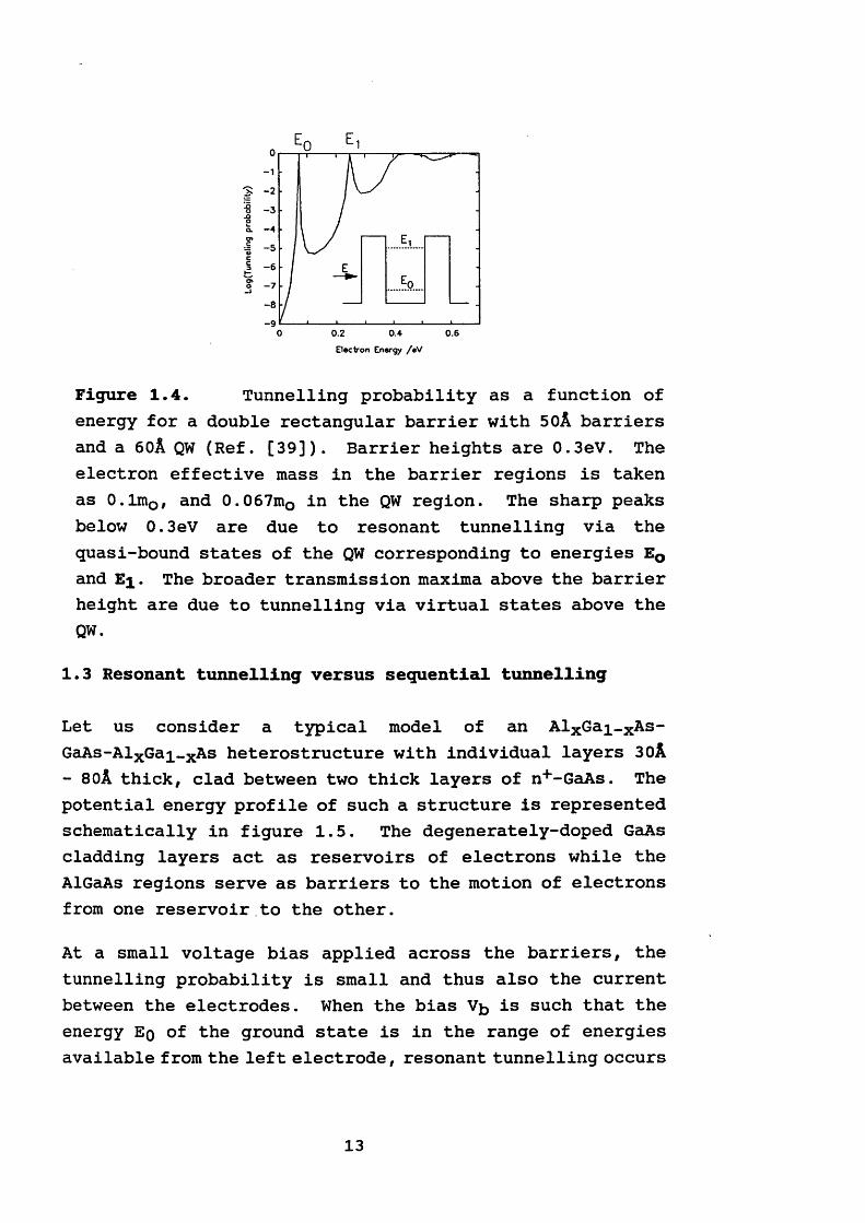
An analytical expression for t(E z} may be obtained by thismethod [41] for the case of rectangular-barrier potential energy profiles. A typical result is shown in figure 1.4 for a symmetrical double-barrier of height 0.3 eV. The
11
barrier widths are 5 nm while the QW width is 6 nm. The electron effective mass was assumed to be 0. lmQ in the barrier regions and 0.067mo in the QW [39]. At certain energies below the barrier height (E0 and Ei), electrons incident on the left barrier can appear on the right without attenuation. This situation corresponds to constructive interference between the two plane waves coexisting in the QW. These energies are the eigen-energies of the QW (since the solutions of Schrodinger's equation in this region are standing waves). This phenomenon is called resonant tunnelling.
It also appears from figure 1.4 that for electron energies above the barrier, the transmission probability also reaches unity for certain values where the interference is again constructive. Such levels are often referred to as virtual states and the x(£2) peaks corresponding to these are much broader than those corresponding to quasi-bound states below the barrier height.
In practice, the transmission probability does not reach unity. This is mainly because the barriers are not identical. Indeed, even if they were, application of an electric field across the structure distorts the potential profile and hence destroys symmetry [42]. However, it is possible to apply the transfer-matrix technique to arbitrarily-shaped profiles by approximating them by rectangular steps of arbitrarily small width. The exact tunnelling probability may then be approached as closely as desired by chosing the appropriate step width [39].
12
-1
5 - 2
O_QO -3ql —4 u*I -5I -6
-7-8-90 0.2 0.4 0.6
Electron Energy /e V
Figure 1.4. Tunnelling probability as a function of energy for a double rectangular barrier with 50A barriers and a 60A QW (Ref. [39]). Barrier heights are 0.3eV. The electron effective mass in the barrier regions is taken as 0.1mO/ and 0.067mo in the QW region. The sharp peaks below 0.3eV are due to resonant tunnelling via the quasi-bound states of the QW corresponding to energies E0 and Ei. The broader transmission maxima above the barrier height are due to tunnelling via virtual states above the QW.
1.3 Resonant tunnelling versus sequential tunnelling
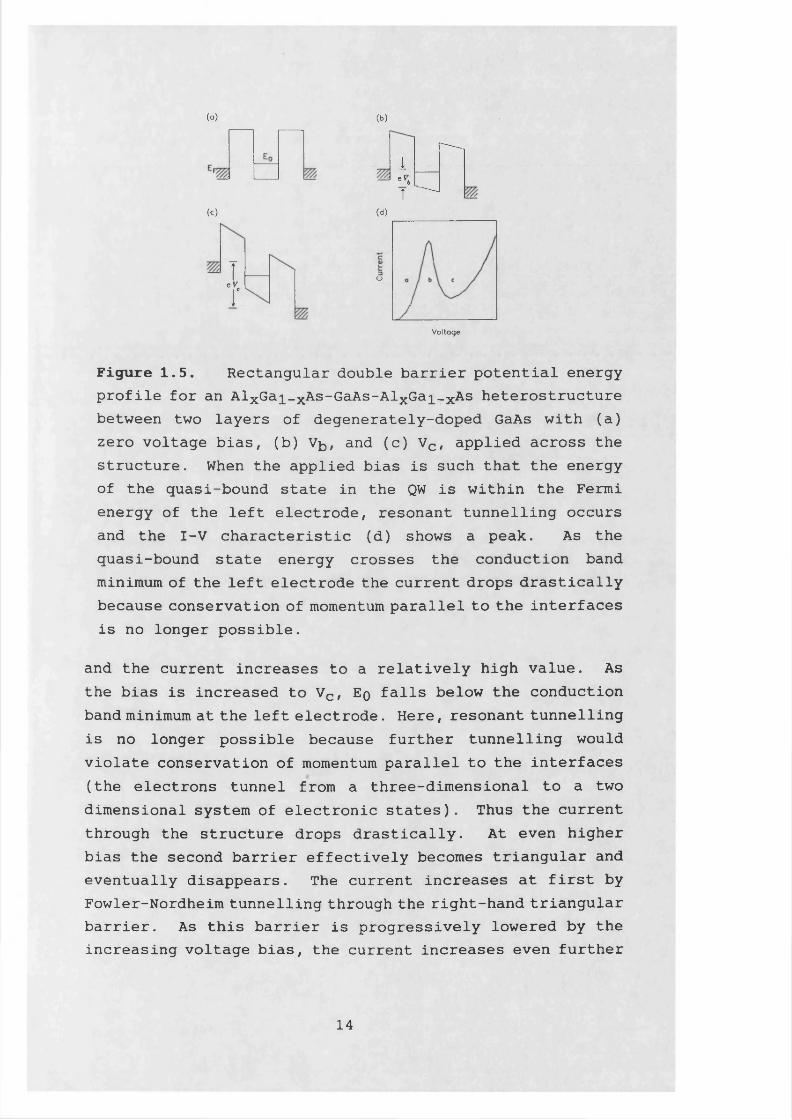
Let us consider a typical model of an AlxGai-xAs- GaAs-AlxGai-xAs heterostructure with individual layers 30A - 80A thick, clad between two thick layers of n+-GaAs. The potential energy profile of such a structure is represented schematically in figure 1.5. The degenerately-doped GaAs cladding layers act as reservoirs of electrons while the AlGaAs regions serve as barriers to the motion of electrons from one reservoir to the other.
At a small voltage bias applied across the barriers, the tunnelling probability is small and thus also the current between the electrodes. When the bias Vfc is such that the energy Eg of the ground state is in the range of energies available from the left electrode, resonant tunnelling occurs
13
(o)
(c)
(b)
1 — I6 6t ^
(d)
TtVBI
O
Voltage
Figure 1.5. Rectangular double barrier potential energy profile for an AlxGai_xAs-GaAs-AlxGai-xAs heterostructure between two layers of degenerately-doped GaAs with (a) zero voltage bias, (b) V^, and (c) Vc, applied across the structure. When the applied bias is such that the energy of the quasi-bound state in the QW is within the Fermi energy of the left electrode, resonant tunnelling occurs and the I-V characteristic (d) shows a peak. As the quasi-bound state energy crosses the conduction band minimum of the left electrode the current drops drastically because conservation of momentum parallel to the interfaces is no longer possible.
and the current increases to a relatively high value. As the bias is increased to Vc, Eq falls below the conduction band minimum at the left electrode. Here, resonant tunnelling is no longer possible because further tunnelling would violate conservation of momentum parallel to the interfaces (the electrons tunnel from a three-dimensional to a two dimensional system of electronic states). Thus the current through the structure drops drastically. At even higher bias the second barrier effectively becomes triangular and eventually disappears. The current increases at first by Fowler-Nordheim tunnelling through the right-hand triangular barrier. As this barrier is progressively lowered by the increasing voltage bias, the current increases even further
14
as now the electrons have only to tunnel through the first barrier to find an increased availability of unoccupied states on the other side with'no reduced dimensionality.
The number of negative resistance features on the I-V characteristic depends only on the width of the QW; for narrow wells (up to about 50A) only the ground state is quasi-bound and this gives rise to a single NDR feature.
The resonant tunnelling process assumes phase coherence across the barrier structure for the wave functions that represent the electrons in these adjacent regions. This, as has been mentioned previously, leads to physically observable negative resistance effects. In actual resonant tunnelling heterostructures, scattering effects are unavoidable. This is seen as the main reason why the peak-to-valley ratio in the NDR region decreases drastically as the device temperature approaches 300K.
One of the effects of inelastic scattering on tunnelling resonances is the decrease in the peak transmission probability [43]. If phase coherence is completely lost because of this underlying process, then it is no longer justifiable to refer to any residual NDR as due to resonant tunnelling. Luryi [44,45] demonstrated that for negative resistance to occur, the necessary and sufficient element is a QW and therefore the second barrier can be infinitely wide [18]. In such extreme situations, the proper term to describe the physical processes leading to negative resistance effects is sequential, non-resonant, or incoherent tunnelling [44,45].
Since the barriers considered here are of finite width, the states in the QW region are quasi-bound, since a particle localised in the well at a time f=0 can tunnel out of it. The lifetime associated with such states is related to the tunnelling probability near resonance, and, by the uncertainty principle, to the width of the resonant state. The
15
resonant tunnelling process may be visualised as starting with a wavepacket incident on the left of a barrier structure similar to the one in figure 1.5. If the energy distribution of the packet is peaked at one of the eigen-energies of the QW, the waves are trapped in the well which now acts as an electronic equivalent to a Fabri-Perot resonator with the waves reflecting back and forth between the barriers with such a phase as to continually reinforce themselves and leaking out slowly. Hence, resonant tunnelling is a 'slow' process. The average time xtrans taken by an electron to leak out of the QW is related to the tunnelling probability and to the average number of times it strikes the barrier per second. It may be shown that xtrans is related to the width of the resonant state A E by [39]
xtransAF * 2nfi (1*24)
in accordance with the uncertainty principle.
Since the resonant tunnelling process requires the build-up of the wave function in the QW region, the process leads to the accumulation of electric charge in the well (this will, in turn, modify the potential energy profile and further complicate calculations of the tunnelling probability; a realisation which has prompted self-consistent calculations of x ( £ J [46,47]).
Because of the exponential nature of the tunnelling probability off resonance, a small increase of the barrier width drastically increases the transit time xtrans (similar effects are observed by increasing barrier heights or electron effective masses). Now, the material parameter that determines whether resonant or sequential tunnelling dominates is the barrier width. If this is small then the transit time xtrans is bound to be smaller than the scattering time xs and resonant tunnelling may be the dominant mechanism leading to negative resistance. In the other extreme of thick barriers, Ttrans ^ anc* sequential tunnelling takes
16
over [48], However, the techniques of section 1.2 are equally applicable to both mechanisms [49]. The basic difference is that the tunnelling probability near 'resonance' will be of order unity in the resonant tunnelling limit and of the order of the tunnelling probability through a single barrier [50] in the other (sequential tunnelling).
1.4 Equivalent circuit models
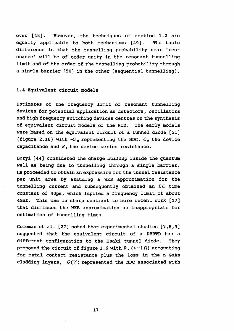
Estimates of the frequency limit of resonant tunnelling devices for potential application as detectors, oscillators and high frequency switching devices centres on the synthesis of equivalent circuit models of the RTD. The early models were based on the equivalent circuit of a tunnel diode [51] (figure 2.16) with -Gd representing the NDC, Cd the device capacitance and R s the device series resistance.
Luryi [44] considered the charge buildup inside the quantum well as being due to tunnelling through a single barrier. He proceeded to obtain an expression for the tunnel resistance per unit area by assuming a WKB approximation for the tunnelling current and subsequently obtained an RC time constant of 40ps, which implied a frequency limit of about 4GHz. This was in sharp contrast to more recent work [17] that dismisses the WKB approximation as inappropriate for estimation of tunnelling times.
Coleman et al. [27] noted that experimental studies [7,8,9] suggested that the equivalent circuit of a DBRTD has a different configuration to the Esaki tunnel diode. They proposed the circuit of figure 1.6 with R s (<~1D) accounting for metal contact resistance plus the loss in the n-GaAs cladding layers, -G(K) represented the NDC associated with
17
the double-barrier-QW, c the 'quantum capacitor' (similar in essence to Luryi's [44]), and R being a resistance which avoids shunting -G through C at high frequencies^-.
Figure 1.6. Equivalent circuit proposed by Coleman et al. [27], The NDC is represented by -£(10, while R s and C are respectively the series resistance and device capacitance. R was introduced empirically to explain high-frequency detection experiments.
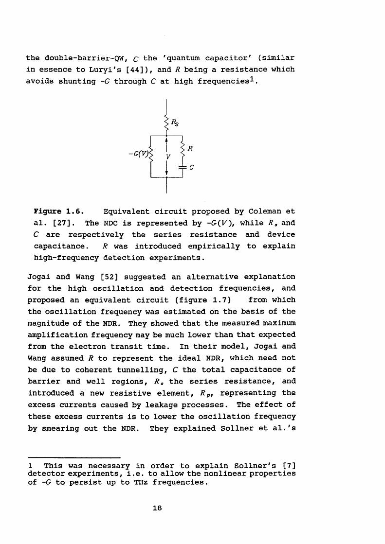
Jogai and Wang [52] suggested an alternative explanation for the high oscillation and detection frequencies, and proposed an equivalent circuit (figure 1.7) from which the oscillation frequency was estimated on the basis of the magnitude of the NDR. They showed that the measured maximum simplification frequency may be much lower than that expected from the electron transit time. In their model, Jogai and Wang assumed R to represent the ideal NDR, which need not be due to coherent tunnelling, C the total capacitance of barrier and well regions, R s the series resistance, and introduced a new resistive element, R PI representing the excess currents caused by leakage processes. The effect of these excess currents is to lower the oscillation frequency by smearing out the NDR. They explained Sollner et al.'s
1 This was necessary in order to explain Sollner's [7] detector experiments, i.e. to allow the nonlinear properties of -G to persist up to THz frequencies.
18
detection at 2.5THz as being due to the frequency-independence of the second derivative of the terminal current as long as R s was small and providing the NDR is not degraded at high frequencies.
-r
Lv w —
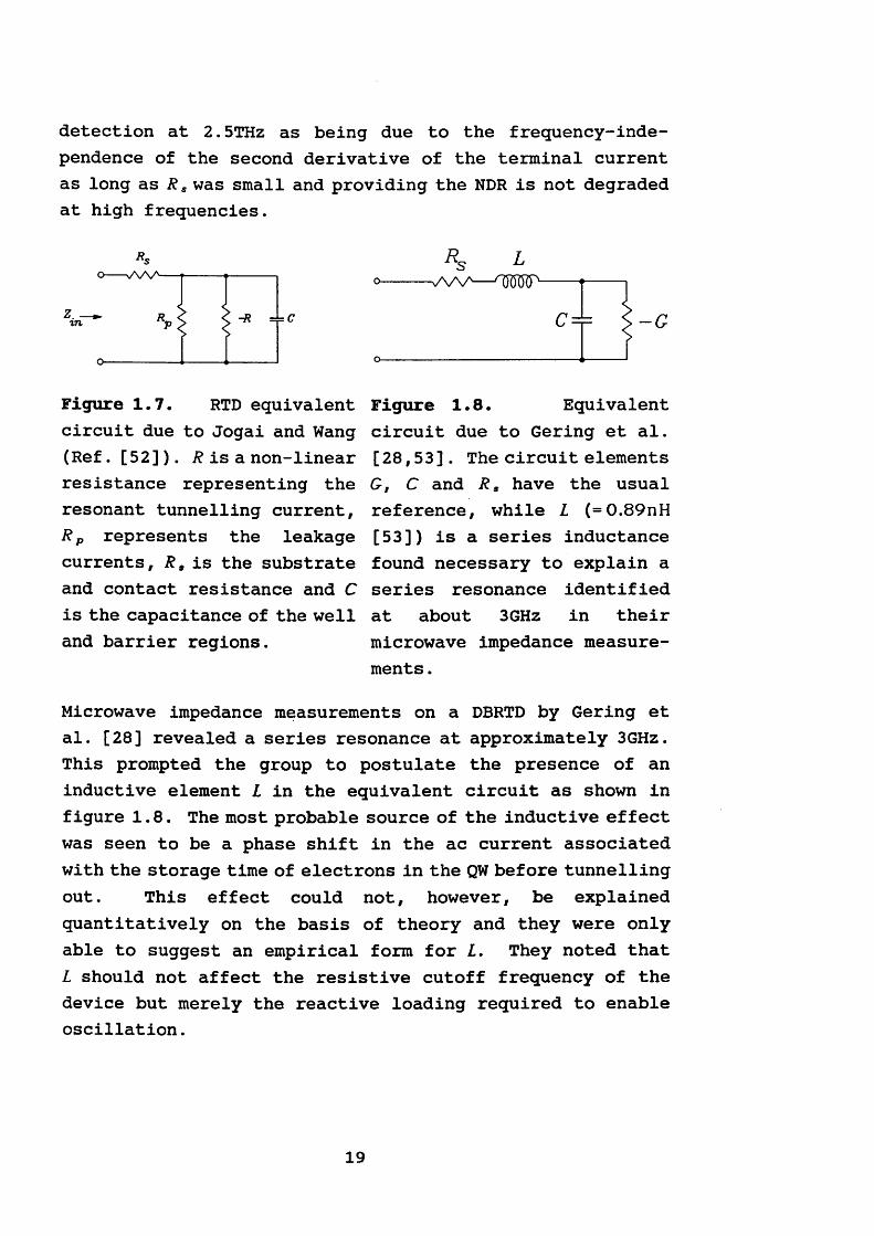
Figure 1.7. RTD equivalent circuit due to Jogai and Wang (Ref. [52]). R is a non-linear resistance representing the resonant tunnelling current, R p represents the leakage currents, is the substrate and contact resistance and C is the capacitance of the well and barrier regions.
Figure 1.8. Equivalentcircuit due to Gering et al. [28,53]. The circuit elements G, C and R s have the usual reference, while L (=0.89nH [53]) is a series inductance found necessary to explain a series resonance identified at about 3 GHz in their microwave impedance measurements .
Microwave impedance measurements on a DBRTD by Gering et al. [28] revealed a series resonance at approximately 3GHz. This prompted the group to postulate the presence of an inductive element L in the equivalent circuit as shown in figure 1.8. The most probable source of the inductive effect was seen to be a phase shift in the ac current associated with the storage time of electrons in the QW before tunnelling out. This effect could not, however, be explained quantitatively on the basis of theory and they were only able to suggest an empirical form for Z. They noted that L should not affect the resistive cutoff frequency of the device but merely the reactive loading required to enable oscillation.
19
Frensley [29] had predicted that the imaginary part of the admittance is negative and proportional to frequency at lower frequencies and that, therefore, this resembled an inductance. However his inductance is several orders of magnitude smaller than the series inductance of Gering et al.. His calculations also revealed that NDC should persist to 5THz, although parasitic circuit elements limit the maximum oscillation frequency to a lower value. Similar inductive behaviour was predicted from an indepen- dent-electron solution to the time-dependent Schrodinger equation [53],
In subsequent work [54], Gering et al. gathered more experimental evidence in support of their series inductive element from studies of a RTD used as a microwave detector. They showed that the detector rectified current can be accurately predicted on the basis of their small-signal equivalent circuit. They also concluded that a RTD biased at its resonant peak would be an inherently better detector than a conventional Schottky barrier diode since the former implements full-wave rectification of an incident signal as opposed to the latter's half-wave rectification.
Recently, Brown et al. [55] have attempted to incorporate the physical effect of a finite quasi-bound state lifetime into an equivalent circuit model by analysing the response of a DBRT structure to a time-varying potential of the form of an abrupt voltage step A V . A finite time interval elapses before the wave function reaches its final steady-state form at a bias of V B + A V . The associated current through the device was assumed to be governed by this time interval xN (being the lifetime of the Nth quasi-bound state) acting as an exponential time constant. The small-signal admittance y(to) of the active region was obtained as
where g is the differential small-signal conductance. From(1.25), the small-signal impedance z(a>) is 1 /g + juoxN/g, and therefore a tunnelling inductance may be defined as l = xN/g.
L
=r C- G
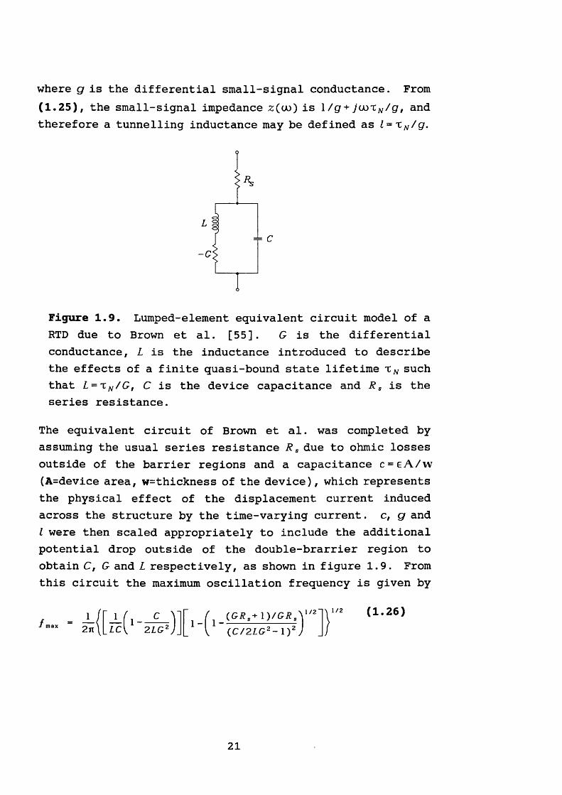
IFigure 1.9. Lumped-element equivalent circuit model of a RTD due to Brown et al. [55]. G is the differential conductance, L is the inductance introduced to describe the effects of a finite quasi-bound state lifetime xN such that L=xN/Gt C is the device capacitance and R s is the series resistance.
The equivalent circuit of Brown et al. was completed by assuming the usual series resistance R s due to ohmic losses outside of the barrier regions and a capacitance c = e A / w (A=device area, w=thickness of the device), which represents the physical effect of the displacement current induced across the structure by the time-varying current. c, g and I were then scaled appropriately to include the additional potential drop outside of the double-brarrier region to obtain C, G and L respectively, as shown in figure 1.9. From this circuit the maximum oscillation frequency is given by
(1.26)f m a x
21
In the limit as L -» 0 (or equivalently 'Ew ->0), the equivalent circuit reverts to the earlier form of a single pole C-model (figure 2.16), where fmax is given by equation (2.3) of chapter 2 .
The oscillator power output was calculated on the basis of an assumption of a sinusoidal voltage waveform t'oCO = A sin (co0f) across the device active region. This enabled expression of the large-signal conductance as
where A and T are the signal amplitude and period respectively and io is the device current. R s and C were assumed to remain unchanged under large-signal conditions whilst the inductance becomes LA = xN/GA.
The power delivered to a load under steady-state conditions was then calculated as
where Z D is the device large-signal impedance. Equation(1.28) was used to obtain estimates of the maximum oscillation power for an AlGaAs-GaAs-AlGaAs DBRTD and compare these with experimental results. The agreement was qualitatively quite good and showed a marked improvement in the prediction accuracy of the cutoff frequency over the previous £C-model, at least up to about 50GHz. Indeed, in a more recent work [25] improved accuracy in the prediction of / max has been shown to be obtainable up to higher frequencies of -450 GHz and possibly above by taking into account the frequen- cy-dependence of R t via the skin effect and using an improved estimate of C which includes the effects of the accumulation and depletion regions outside the QW and charge accumulation within the QW at resonance. It now seems that the oscillation
(1.27)
1 /12S(Z0) 2\R,-2d\2
(1.28)
22

frequency limit is primarily determined by the series resistance while the magnitude of the NDC determines the maximum output power, although the two effects are not independent.
23
References1. L. Esaki, "New phenomenon in narrow germanium p-n junctions", Phys. Rev., Vol. 109, 1958, pp. 601-604.2. L. Esaki, "Long journey into tunneling", Science, Vol. 183, 1974, pp. 1149-1155.3. C. B. Duke, "Tunneling in Solids," Academic Press, New York, 1969.4. R. Tsu and L. Esaki, "Tunneling in a finite superlattice", Appl. Phys. Lett., Vol. 22, 1973, pp. 562-564.5. L. L. Chang, L. Esaki, and R. Tsu, "Resonant tunneling in semiconductor double barriers", Appl. Phys. Lett., Vol. 24, 1974, pp. 593-595.6 . L. Esaki and L. L. Chang, "New transport phenomenon in a semiconductor 'superlattice'", Phys. Rev. Lett., Vol. 33, 1974, pp. 495-498.7. T. C. L. G. Sollner, W. D. Goodhue, P. E. Tannenwald, C. D. Parker, and D. D. Peck, "Resonant tunneling through quantum wells at frequencies up to 2.5 THz", Appl. Phys. Lett., Vol. 43, 1983, pp. 588-590.8 . T. C. L. G. Sollner, W. D. Goodhue, P. E. Tannenwald, C. D. Parker, and D. D. Peck, "Resonant tunneling through quantum wells at 2.5 THz", IEEE Trans Electron Devices, Vol. ED-30, 1983, p. 1577.9. T. C. L. G. Sollner, P. E. Tannenwald, D. D. Peck, and W. D. Goodhue, "Quantumwell oscillators", Appl. Phys. Lett., Vol. 45, 1984, pp. 1319-1321.10. T. J. Shewchuk, P. C. Chapin, P. D. Coleman, W. Kopp, R. Fischer, and H. Morkog, "Resonant tunneling in a GaAs-AlxGai_xAs heterostructure at room temperature", Appl. Phys. Lett., Vol. 46, 1985, pp. 508-510.11. A. R. Bonnefoi, R. T. Collins, T. C. McGill, R. D. Burnham, and F. A. Ponce, "Resonant tunneling in GaAs-AlAs heterostructures by metalorganic chemical vapour deposition", Appl. Phys. Lett., Vol. 46, 1985, pp. 285-287.12. E. E. Mendez, W. I. Wang, and L. Esaki, "Resonant tunneling of holes in AlAs-GaAs-AlAs heterostructures", Appl. Phys. Lett., Vol. 47, 1985, pp. 415-417.13. W. D. Goodhue, T. C. L. G. Sollner, H. Q. Le, E. R. Brown, and B. A. Vojak, "Large room-temperature effects from resonant tunneling through AlAs barriers", Appl. Phys. Lett., Vol. 49, 1986, pp. 1086-1088.14. C. I. Huang, M. J. Paulus, C. A. Bozada, S. C. Dudley, K. R. Evans, C. E. Stutz, R. L. Jones, and M. E. Cheney, "AlGaAs-GaAs double barrier diodes with high peak-to-valley current ratio", Appl. Phys. Lett., Vol. 51, 1987, pp. 121-123.
24
15. E. R. Brown, T. C. L. G. Sollner, W. D. Goodhue, and C. D. Parker, "Fundamental oscillations up to 200 GHz in a resonant-tunneling diode", IEEE Trans. Electron Dev., Vol. ED-34, 1987, p. 2381.16. E. R. Brown, T. C. L. G. Sollner, W. D. Goodhue, and C. D. Parker, "Millimeter-band oscillations based on resonant tunneling in a double-barrier diode at room temperature", Appl. Phys. Lett., Vol. 50, 1987, pp. 83-85.17. T. C. L. G. Sollner, E. R. Brown, W. D. Goodhue, and H. Q. Le, "Observation of millimeter-wave oscillations from resonant tunneling diodes and some theoretical considerations of ultimate frequency limits", Appl. Phys. Lett., Vol. 50, 1987, pp. 332-334.18. H. Morkog, J. Chen, U. K. Reddy, T. Henderson, and S. Luryi, "Observation of a negative differential resistance due to tunneling through a single barrier into a quantum well", Appl. Phys. Lett., Vol. 49, 1986, pp. 70-72.19. T. Nakagawa, H. Imamoto, T. Kojima, and K. Ohta, "Observation of resonant tunneling in AlGaAs/GaAs triple barrier diodes", Appl. Phys. Lett., Vol. 49, 1986, pp. 73-75.20. M. A. Reed, J. W. Lee, and H-L. Tsai, "Resonant tunneling through a double GaAs/AlAs superlattice barrier, single quantum well heterostructure", Appl. Phys. Lett., Vol. 49, 1986, pp. 158-160.21. T. Inata, S. Muto, Y. Nakata, T. Fuji, H. Ohnishi, and S. Hiyamizu, "Excellent negative differential resistance of InAlAs/lnGaAs resonant tunneling barrier structures grown by MBE", Jpn. J. Appl. Phys., Vol. 25, 1986, pp. L983-L985.22. T. Inata, S. Muto, Y. Nakata, S. Sasa, T. Fuji, and S. Hijamizu, "A Pseudomorphic Ino.5 3 Gao.4 7 AS/AIAS resonant tunneling barrier with peak-to-valley current ratio of 14 at room temperature", Jpn. J. Appl. Phys., Vol. 26, 1987, pp. L1332-L1334.23. T. P. E. Broekaert, W. Lee, andC. Fonstad, "Pseudomorphic InO.53GaO.47As/AlAs/InAs resonant tunneling diodes with peak-to-valley current ratios of 30 at room temperature", Appl. Phys. Lett., Vol. 53, 1988, pp. 1545-1547.24. E. R. Brown, W. D. Goodhue, and T. C. L. G. Sollner, "Fundamental oscillations up to 200 GHz in resonant tunneling diodes and new features of their maximum oscillation frequency from stationary-state tunneling theory", J. Appl. Phys., Vol. 64, 1988, pp. 1519-1529.25. E. R. Brown, T. C. L. G. Sollner, C. D. Parker, W. D. Goodhue, and C. L. Chen, "Oscillations up to 420 GHz in GaAs/AlAs resonant tunneling diodes", Appl. Phys. Lett., Vol. 55, 1989, pp. 1777-1779.
25
26. see e.g., T. C. L. G. Sollner, H. Q. Le, C. A. Correa, and W . D . Goodhue, Proc. IEEE Cornell Conf • Advanced Concepts High Speed Semiconductor Devices and Circuits, Cornell University, Ithaca, New York, 1985, 252; F. Capasso, S.Sen, A. C. Gossard, A. L. Hutchinson, and J. E. English, IEEE Electron Dev. Lett., EDL-7 (1986), 573; N. Yokoyama, K. Imamura, S. Muto, S. Hiyamizu, and H. Nishii, Jpn. J. Appl. Phys., 24 (1985), L583; C. H. Yang, Y. C. Kao, and H. D. Shih, Appl. Phys. Lett., 55 (1989), 2742.27. T. J. Shewchuk, P. C. Chapin, J. M. Gering, P. D. Coleman, W. Kopp, and H. Morkog, "Microwave admittance characterisation of GaAs-AlxGai_xAs resonant tunneling heterostructures", Proc. IEEE Cornell Conf. Advanced Concepts High Speed Semiconductor Devices and Circuits, Cornell University, Ithaca, New York, 1985, pp. 370-379.28. P. D. Coleman, S. Goedeke, T. J. Shewchuk, and P. C. Chapin, "Experimental study of the frequency limit of a resonant tunneling oscillator", Appl. Phys. Lett., Vol. 48, 1986, pp. 422-424.29. J. M. Gering, D. A. Crim, D. G. Morgan, P. D. Coleman, W. Kopp, and H. Morkog, "A small-signal equivalent circuit for GaAs-AlxGai_xAs resonant tunneling heterostructures at microwave frequencies", J. Appl. Phys., Vol. 61, 1987, pp. 271-276.30. W. R. Frensley, "Quantum transport calculation of the small-signal response of a resonant tunneling diode", Appl. Phys. Lett., Vol. 51, 1987, pp. 448-450.31. V. P. Kesan, D. P. Neikirk, P. A. Blakey, B. G. Streetman, andT. D. Linton, Jr., "The influence of transit-time effects on the optimum design and maximum oscillation frequency of quantum well oscillators", IEEE Trans. Electron Dev., Vol. ED-35, 1988, pp. 405-413.32. D. Lippens and P. Mounaix, "Small-signal impedance of GaAs-AlxGai_xAs resonant tunnelling heterostructures at microwave frequency", Electronics Lett., Vol. 24, 1988,pp. 1180-1181.33. see e.g., S. Luryi, Appl. Phys. Lett., 47 (1985), 490; D.D.Coon and H. C. Liu, Appl. Phys. Lett., 49 (1986), 94; W. Frensley, IEEE Int. Electron Devices Meeting (1986), paper 25.5, etc.34. R. A. Davies, "Simulations of the current-volatge characteristics of semiconductor tunnel structures", GEC J. Res., Vol. 9, 1987, pp. 65-75.35. S. Adachi, "GaAs, AlAs, and AlxGai_xAs: material parameters for use in research and device applications", J. Appl. Phys., Vol. 58, 1985, pp. R1-R29.36. H. Kroemer, "Band offsets at heterointerfaces: theoretical basis, and review of recent experimental work", Surface Sci., Vol. 174, 1986, pp. 299-306.
26
37. W. A. Harrison, "Tunneling from an independent-particle point of view", Phys. Rev., Vol. 123, 1961, pp. 85-89.38. R. Eppenga and M. F. H. Schuurmans, "Theory of the GaAs/AlGaAs quantum well", Philips Tech. Rev., Vol. 44,1988, pp. 137-149.39. E. E. Mendez, "Physics of resonant tunnelling in semiconductors", in E. E. Mendez and K. von Klitzing, ed., "Pysics and Applications of Quantum Wells and Superlattices," Plenum Press, London, 1987, pp. 159-188.40. K. F. Brennan and C. J. Summers, "Theory of resonant tunneling in a variably spaced multiquantum well structure: an Airy function approach", J. Appl. Phys., Vol. 61, 1987, pp. 614-623.41. E. 0. Kane, "Basic Concepts of Tunneling", in E. Burnstein and S. Lundqvist, ed., "Tunneling Phenomena in Solids", Plenum Press, New York, 1969.42. B. Ricco andM. Ya. Azbel, "Physics of resonant tunneling. The one-dimensional case", Phys. Rev. B, Vol. 29, 1984, pp. 1970-1981.43. A. D. Stone and P. A. Lee, "Effect of inelastic processes on resonant tunneling in one dimension", Phys. Rev. Lett., Vol. 54, 1985, pp. 1196-1199.44. S. Luryi, "Frequency Limit of double-barrier resonant tunneling oscillators", Appl. Phys. Lett., Vol. 47, 1985, pp. 490-492.45. S. Luryi, "Coherent versus incoherent resonant tunneling and implications for fast devices", Superlattices and Microstructures, Vol. 5, 1989, pp. 375-382.46. H. Ohnishi, T. Inata, S. Muto, N. Yokoyama, A. Shibatomi, "Self-consistent analysis of resonant tunneling current", Appl. Phys. Lett., Vol. 49, 1986, pp. 1248-1250.47. M. Cahay, M. McLennan, S. Ditta, and M. S. Lundstrom, "Importance of space-charge effects in resonant tunneling devcies", Appl. Phys. Lett., Vol. 50, 1987, pp. 612-614.48. H. Schneider, K. von Klitzing and K. Ploog, "Resonant and non-resonant tunneling in GaAs/AlAs multiquantum well structures", Superlattices and Microstructures, Vol. 5,1989, pp. 383-396.49. T. Weil and B. Vinter, "Equivalence between resonant tunneling an sequential tunneling in double-barrier diodes", Appl. Phys. Lett., Vol. 50, 1987, pp. 1281-1283.50. M. Biittiker, "The role of quantum coherence in series resistors", Phys. Rev. B, Vol. 33, 1986, pp. 3020-3026.51. "Standards of Definitions, Symbols and Methods of Test for Semiconductor Tunnel (Esaki) Diodes and Backward Diodes," IEEE Trans. Electron Devices, ED-12 (1965), 374.
27
52. B. Jogai and K. L. Wang, "Frequency and power limit of quantum well oscillators", Appl. Phys. Lett., Vol. 48, 1986, pp. 1003-1005.53. R. K. Mains and G. I. Haddad, "Time-dependent modelling of resonant tunneling diodes from direct solution of the Schrodinger equation", J. Appl. Phys., Vol. 64. 1988, pp. 3564-3569.54. J. M. Gering, T. J. Rudnick, and P. D. Coleman, "Microwave detection using the resonant tunneling diode", IEEE Trans. Microwave Theory Tech., Vol. MTT-36, 1988, pp. 1145-1150.55. E. R. Brown, C. D. Parker, and T. C. L. G. Sollner, "Effect of quasibound-state lifetime on the oscillation frequency of resonant tunneling diodes", Appl. Phys. Lett., Vol. 54, 1989, pp. 934-936.56. S. Ray, P. Ruden, V. Sokolov, R. Kolbas, T. Boonstra, and J. Williams, "Resonant tunneling transport at 300 K in GaAs/AlGaAs quantum wells grown by metalorganic chemical vapour depositions", Appl. Phys. Lett., Vol. 48, 1986, pp. 1666-1668.57. P. D. Hodson, D. J. Robbins, R. H. Wallis, J. I. Davies, and A. C. Marshall, "Resonant tunnelling in AlInAs/GalnAs double barrier diodes grown by MOCVD", Electron. Lett., Vol. 24, 1988, pp. 187-188.58. R. D. Scnell, H. Tews, and R. Neumann, "Room temperature operation of AlGaAs/GaAs resonant tunnelling structures grown by metalorganic vapour-phaes epitaxy", Electron. Lett., Vol. 25, pp. 830-831.59. L. F. Lou, R. Beresford, and W. I. Wang, "Resonant tunneling in AlSb/InAs/AlSb double-barrier heterostructures", Appl. Phys. Lett., Vol. 53, 1988, pp. 2320-2322.60. J. R. Soderstrom, D. H. Chow, and T. C. McGill, "InAs/AlSb double-barrier structure with large peak-to-valley current ratio: a candidate for high-frequency microwave devices", IEEE Electron Dev. Lett., Vol. 11, 1990, pp. 27-29.61. C. J. Gulatieri, C. D. Schwarz, R. G. Nuzzo, R. J. Malik, and J. P. Walker, "Determination of the (100) InAs/GaSb heterojunction valence-band discontinuity by X-ray photoemission core level spectroscopy", J. Appl. Phys.B, Vol.61. 1987, pp. 5337-5341.62. C. J. Gulatieri, C. D. Schwarz, R. G. Nuzzo, and W. A. Sunder, "X-ray photoemission core level determination of the GaSb/AlSb heterojunction valence-band discontinuity", Appl. Phys. Lett., Vol. 49, 1986, pp. 1037-1039.63. J. R. Soderstrom, E. R. Brown, C. D. Parker, L. J. Mahoney, J. Y. Yao, T. G. Anderson, and T. C. McGill, "Growth and characterisation of high density, high-speed InAs/AlSb resonant tunneling diodes", Appl. Phys. Lett., Vol. 58, 1991, pp. 275-277.
28
64. J. R. Soderstrom, J. Y. Yao, and T. G. Anderson, "Observation of resonant tunneling in InSb/AlInSb doublebarrier structures", Appl. Phys. Lett., Vol. 58, 1991, pp. 708-710.65. E. R. Brown, J. R. Soderstrom, C. D. Parker, L. J. Mahoney, K. M. Molvar, and T. C. McGill, "Oscillations up to 712 Ghz in InAs/AlSb resonant tunneling diodes", Appl. Phys. Lett., Vol. 58, 1991, pp. 2291-2293.
29
CHAPTER 2
DC CHARACTERISATION AND BIAS CIRCUIT INSTABILITY
2.1 Introduction
For a negative conductance device the potential capabilities as an active element in a microwave oscillator circuit may be tentatively assessed by considering two parameters; the maximum frequency of operation and the maximum radio frequency (rf) power output. However, the biasing circuit may effect both.
Using a simple equivalent circuit model for a resonant tunnelling device it is possible to analyse the circuit behaviour when the device is biased in different regions of its dc current-voltage (I-V) characteristic. Dc characterisation is therefore important as the results give clear indications of the suitability or otherwise of these negative conductance devices as potential active microwave circuit elements and the problems such applications are likely to encounter. Moreover, the experimental data thus obtained can be used to construct empirical equivalent circuit models for RTD's which form the basis of small- and large-signal analysis, as will be described here and in chapters 4 and5.
This chapter starts by describing some of the double barrier resonant tunnelling structures (DBRTD's) tested and their subsequent dc characteristics. The experimental I-V curves shown here were determined using the dc characterisation station described in Appendix I.
30
The rest of the chapter is concerned with dc instability inherent with most of the tested devices. The recent controversy about the nature of hysteresis and bistability in the dc I-V characteristics of DBRTD's is discussed. Time-domain numerical simulations reported here will show that it is possible to explain this phenomenon on the basis of device-circuit interaction.
The necessary criteria for low frequency stability are derived and experimental observations of bias circuit oscillation are explained in detail and compared with the numerical simulations.
The final section discusses the influence of dc stabilisation on the rf power generation capabilities of RTD's.
2.2 The tested devices
This section is concerned with describing the structures of the devices tested and some results obtained from their dc characterisation.
Section 2.2.1 describes structures and dc characterisation results obtained from some MBE-grown heterostructures while section 2 .2 . 2 is concerned with the evaluation of some structures grown by MOCVD.
2.2.1 The MBE devices
Three of the MBE structures tested were grown at Philips Research Laboratories (PRL), Redhill, Surrey. The fourth
« was provided by DRA (formerly RSRE), Malvern. The devices were code named as follows:
PRL devices 6294MV1484M269
31
DRA devices GWS160
All the wafer samples had Ni/Ge/Au top and bottom ohmic contacts. Devices were defined as mesas by wet chemical etching. The latest batch of M269 devices were, however, plasma-etched.
Growth schedules for the G294 wafer are not available, thus the exact details of the structure are not known. The AlxGai_xAs barriers have x = 0.67, and they, along with the GaAs quantum well (QW) were not intentionally doped. It is not known whether undoped spacer layers have been incorporated into this structure.
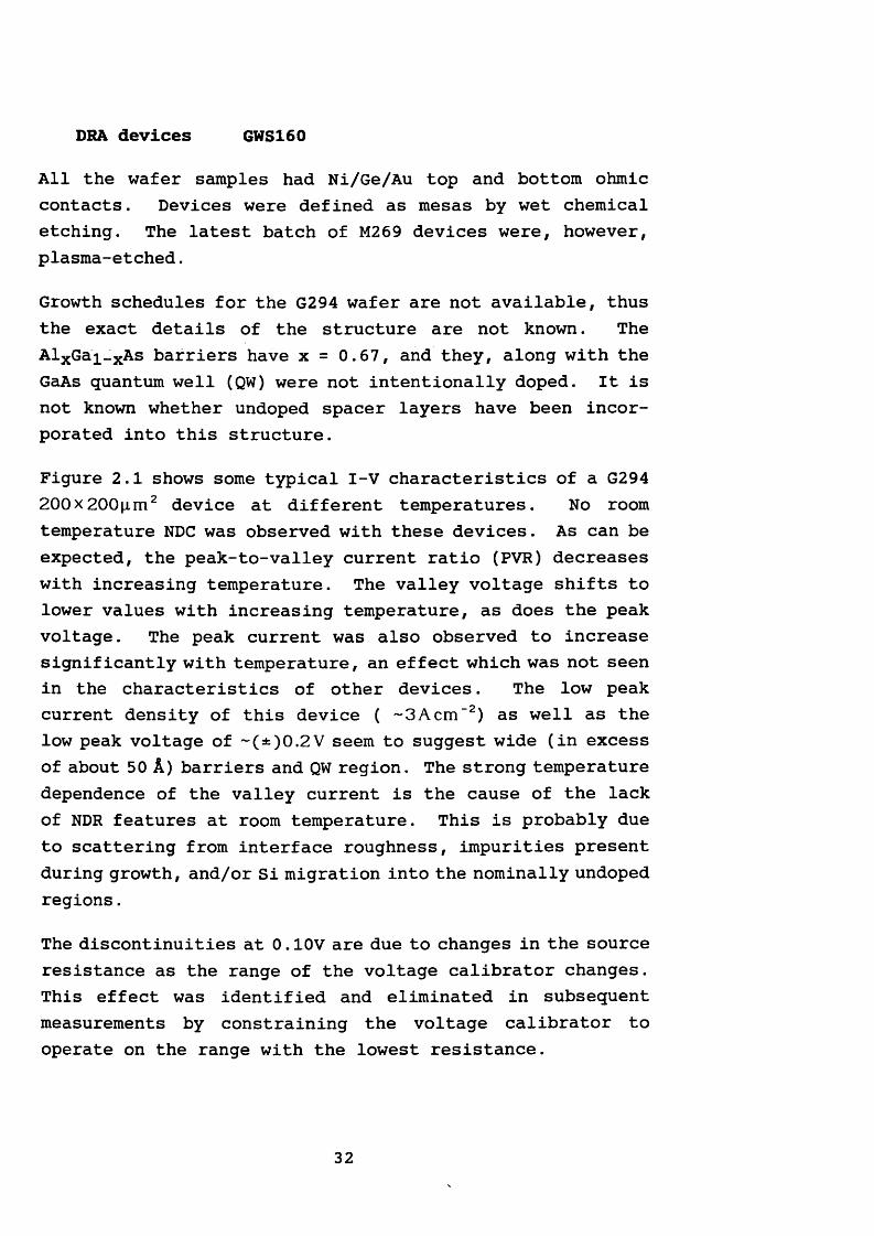
Figure 2.1 shows some typical I-V characteristics of a G294 200x 200^m 2 device at different temperatures. No room temperature NDC was observed with these devices. As can be expected, the peak-to-valley current ratio (PVR) decreases with increasing temperature. The valley voltage shifts to lower values with increasing temperature, as does the peak voltage. The peak current was also observed to increase significantly with temperature, an effect which was not seen in the characteristics of other devices. The low peak current density of this device ( ~ 3 A c m -2) as well as the low peak voltage of ~(±)0 .2 V seem to suggest wide (in excess of about 50 A ) barriers and QW region. The strong temperature dependence of the valley current is the cause of the lack of NDR features at room temperature. This is probably due to scattering from interface roughness, impurities present during growth, and/or Si migration into the nominally undoped regions.
The discontinuities at 0.10V are due to changes in the source resistance as the range of the voltage calibrator changes. This effect was identified and eliminated in subsequent measurements by constraining the voltage calibrator to operate on the range with the lowest resistance.
32
20
10
<E
77K
-1 0140K- 1 5
-20 200K
- 2 5- 0 . 4 0 .4- 0.2 0 0.2
V o ltage / V
Figure 2.1. I-V characteristics at different temperatures for a device from wafer G294. The discontinuities at 0.10V are due to changes in source resistance associated with a change of range.
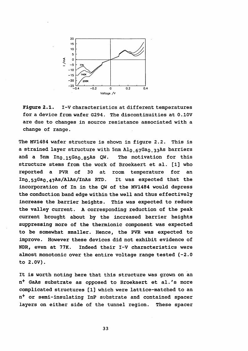
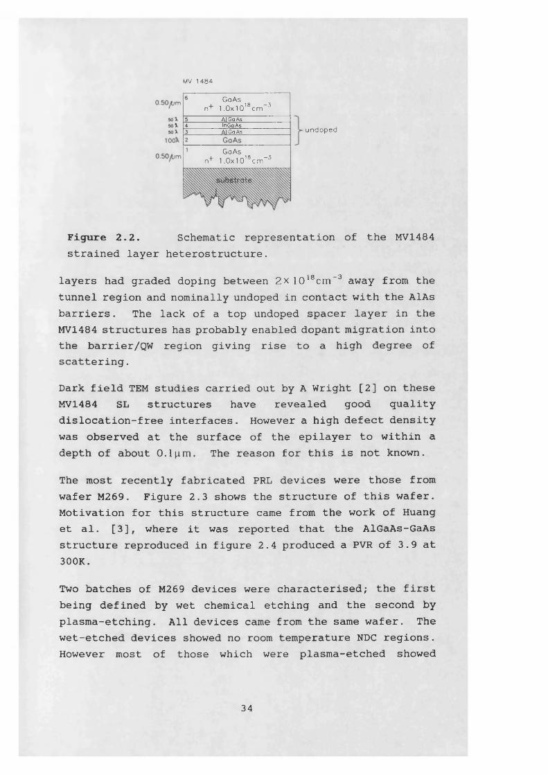
The MV1484 wafer structure is shown in figure 2.2. This is a strained layer structure with 5nm AIq.67Ga0 .33As barriers and a 5nm Ing.l5Gao.85As QW. The motivation for this structure stems from the work of Broekaert et al. [1] who reported a PVR of 30 at room temperature for an Ino.5 3 Gao.4 7 As/AlAs/InAs RTD. It was expected that the incorporation of In in the QW of the MV1484 would depress the conduction band edge within the well and thus effectively increase the barrier heights. This was expected to reduce the valley current. A corresponding reduction of the peak current brought about by the increased barrier heights suppressing more of the thermionic component was expected to be somewhat smaller. Hence, the PVR was expected to improve. However these devices did not exhibit evidence of NDR, even at 77K. Indeed their I-V characteristics were almost monotonic over the entire voltage range tested (-2 . 0 to 2.0V).
It is worth noting here that this structure was grown on an n+ GaAs substrate as opposed to Broekaert et al.'s more complicated structures [1 ] which were lattice-matched to an n+ or semi-insulating InP substrate and contained spacer layers on either side of the tunnel region. These spacer
33
MV 1484
GaAs n+ 1 .0x1018cm ~3
Al Go AsInGaAsA l Go As
GoAs n+ 1 .0x1018cm -3
undoped
Figure 2.2. Schematic representation of the MV1484strained layer heterostructure.
layers had graded doping between 2x 1018cm"3 away from the tunnel region and nominally undoped in contact with the AlAs barriers. The lack of a top undoped spacer layer in the MV1484 structures has probably enabled dopant migration into the barrier/QW region giving rise to a high degree of scattering.
Dark field TEM studies carried out by A Wright [2] on these MV1484 SL structures have revealed good quality dislocation-free interfaces. However a high defect density was observed at the surface of the epilayer to within a depth of about O.lpim. The reason for this is not known.
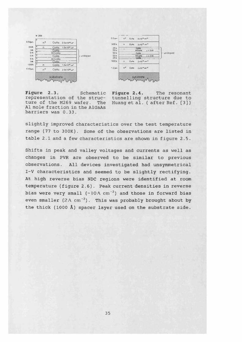
The most recently fabricated PRL devices were those from wafer M269. Figure 2.3 shows the structure of this wafer. Motivation for this structure came from the work of Huang et al. [3], where it was reported that the AlGaAs-GaAs structure reproduced in figure 2.4 produced a PVR of 3.9 at 300K.
Two batches of M269 devices were characterised; the first being defined by wet chemical etching and the second by plasma-etching. All devices came from the same wafer. The wet-etched devices showed no room temperature NDC regions. However most of those which were plasma-etched showed
34
O.SOfums
n + GaAs 2 .0x10 l»«m-
200X 8 n GaAs 1.0X10“ cm134X 7 GaAs5 IX 6
AlGaAs51X 5 GaAsSIX 4 AlGaAs34X I GaAs
1000X 2 n GaAs 1.0x10’ * cm*
0.40pm1
n+ GaAs 2 .0x10 ‘4 cm"*
undoped
0.5 pm
500 X
25 X 50x 50 x 50 x 25 X 500X
1.0 pm
n + GaAs 2 x 1 0 " t i
n GaAs 2x10“ <#n“ *
AlGaAs X - 0.42
GaAsAlGaAs x - 0.42
n GaAs 2 x 1 0 *« » -*
GaAs 2x10“ c
undoped
Figure 2.3. Schematicrepresentation of the structure of the M269 wafer. The Al mole fraction in the AlGaAs barriers was 0.33.
Figure 2.4. The resonant tunnelling structure due to Huang etal. (after Ref. [3])
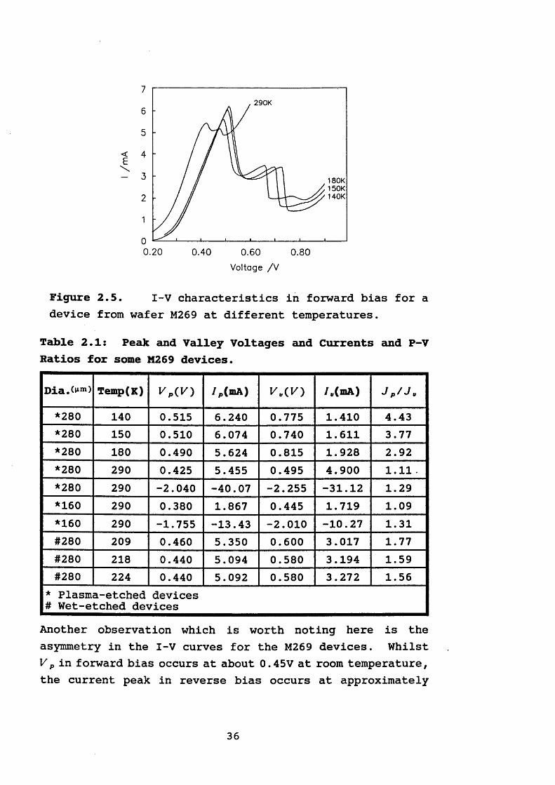
slightly improved characteristics over the test temperature range (77 to 300K) . Some of the observations are listed in table 2.1 and a few characteristics are shown in figure 2.5.
Shifts in peak and valley voltages and currents as well as changes in PVR are observed to be similar to previous observations. All devices investigated had unsymmetrical I-V characteristics and seemed to be slightly rectifying. At high reverse bias NDC regions were identified at room temperature (figure 2.6). Peak current densities in reverse bias were very small (~10A c m -2) and those in forward bias even smaller (2A cm"2) . This was probably brought about by the thick ( 1 0 0 0 A ) spacer layer used on the substrate side.
35
99
72 9 0 K
6
543 1 8 0 K
1 5 0 K1 4 0 K2
1
0 ^ 0.20 0.40 0.60 0.80
Voltage /V
Figure 2.5. I-V characteristics in forward bias for a device from wafer M269 at different temperatures.
Table 2.1: Peak and Valley Voltages and Currents and P-VRatios for some M269 devices.
Dia.^m ) Temp(K) V p(V) /p(mA) 7v(mA) Jp/Jv
*280 140 0.515 6.240 0.775 1.410 4.43*280 150 0.510 6.074 0.740 1.611 3.77*280 180 0.490 5.624 0.815 1.928 2.92*280 290 0.425 5.455 0.495 4.900 1 . 1 1 .*280 290 -2.040 -40.07 -2.255 -31.12 1.29*160 290 0.380 1.867 0.445 1.719 1.09*160 290 -1.755 -13.43 -2 . 0 1 0 i M O N> 1.31#280 209 0.460 5.350 0.600 3.017 1.77#280 218 0.440 5.094 0.580 3.194 1.59#280 224 0.440 5.092 0.580 3.272 1.56
* Plasma-etched devices# Wet-etched devicesAnother observation which is worth noting here is the asymmetry in the I-V curves for the M269 devices. Whilst V p in forward bias occurs at about 0.45V at room temperature, the current peak in reverse bias occurs at approximately
36
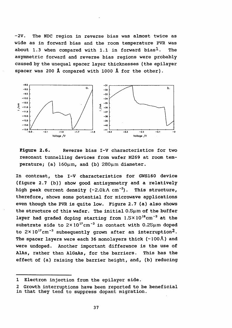
-2V. The NDC region in reverse bias was almost twice as wide as in forward bias and the room temperature PVR was about 1.3 when compared with 1.1 in forward bias1 . The asymmetric forward and reverse bias regions were probably caused by the unequal spacer layer thicknesses (the epilayer spacer was 2 0 0 A compared with 1 0 0 0 A for the other).
-8 .5
-9 .0
-9 .5
-13.5•2.3 . - 2.1 -1.9
-31
-3 2
■33
•34
-3 5
-3 6
~ -3 7
-3 8
-3 9
-4 0
- 2.2-2 .3•2.4Voltage / V Voltage / V
Figure 2.6. Reverse bias I-V characteristics for two resonant tunnelling devices from wafer M269 at room temperature; (a) 160iim, and (b) 280|im diameter.
In contrast, the I-V characteristics for GWS160 device (figure 2.7 (b)) show good antisymmetry and a relatively high peak current density (-2.0k A cm"2). This structure, therefore, shows some potential for microwave applications even though the PVR is quite low. Figure 2.7 (a) also shows the structure of this wafer. The initial 0 .5*1 m of the buffer layer had graded doping starting from 1.5xl018c m "3 at the substrate side to 2 x 10¹⁷c m ’3 in contact with 0.25*xm doped to 2 x 1 0 17c m "3 subsequently grown after an interruption^. The spacer layers were each 36 monolayers thick (-100A) and were undoped. Another important difference is the use of AlAs, rather than AlGaAs, for the barriers. This has the effect of (a) raising the barrier height, and, (b) reducing
1 Electron injection from the epilayer side.2 Growth interruptions have been reported to be beneficialin that they tend to suppress dopant migration.
37
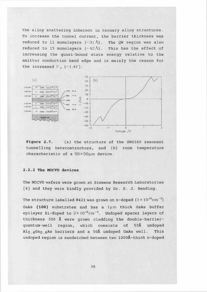
the alloy scattering inherent in ternary alloy structures. To increase the tunnel current, the barrier thickness was reduced to 11 monolayers (-31 A). The QW region was also reduced to 15 monolayers (~42A) . This has the effect of increasing the quasi-bound state energy relative to the emitter conduction band edge and is mainly the reason for the increased V p (-1.4K).
(a)0 .2 5 /Un
0.50 f**
0.25 ftn
0.25 /U"
0 .2 5 /Wn
0.50 ftni
r & GaAs 1.0x10'*«m-3
n GaAs 2.0*101?cm->
n GaAs 2.0x10,7cm*>
it GaAs 2.0x1017cm-»
n GaAs 2.0x101?cm->
n+ GaAs 1.5x10'* cm-A
W M M i
GaAs 36 ml
MAS <1 ml
GaAs
AJAS <1 M
GaAs 36 ml
5 0
4 0
3 0
20
<E
-20- 3 0
- 4 0
- 5 0
- 6 0 0 1 2-2 - 1Voltage / V
Figure 2.7. (a) the structure of the GWS160 resonanttunnelling heterostructure, and (b) room temperature characteristic of a 50x50nm device.
2.2.2 The MOCVD devices
The MOCVD wafers were grown at Siemens Research Laboratories [4] and they were kindly provided by Dr. S. J. Bending.
The structure labelled #421 was grown on n-doped (1 x 1018cm'3)GaAs (100) substrates and has a l^m thick GaAs buffer epilayer Si-doped to 2x 1018cm"3. Undoped spacer layers of thickness 300 A were grown cladding the double-barrier- quantum-well region, which consists of 50A undoped AlQ.4Gao.6As barriers and a 50A undoped GaAs well. This undoped region is sandwiched between two lOOOA-thick n-doped
38
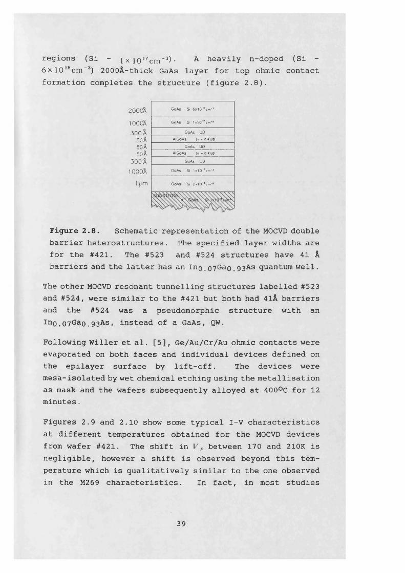
regions (Si - 1 x 1017cm'3) • A heavily n-doped (Si -6 x l 0 18c m ”3) 2000A-thick GaAs layer for top ohmic contact formation completes the structure (figure 2.8).
2000ft GaAs Si 6x10” cn-J
1000ft300 ft
5 0 f t
5 0 f t
5 0 ft
300 ft1000ft
1 p m
GoAs Si 1x10,7«r
GaAs UD
AlGaAs (* - o.4)udGaAs UD
AJGoAs (x - 0.4)U D
GaAs UD
GaAs Si 1x10’7cm-s
GaAs Si 2x10” cm-»
Figure 2.8. Schematic representation of the MOCVD double barrier heterostructures. The specified layer widths are for the #421. The #523 and #524 structures have 41 A barriers and the latter has an Ino.07Ga0 .93As quantum well.
The other MOCVD resonant tunnelling structures labelled #523 and #524, were similar to the #421 but both had 4lA barriers and the #524 was a pseudomorphic structure with an In0 .07Ga0 .93As* instead of a GaAs, QW.
Following Wilier et al. [5], Ge/Au/Cr/Au ohmic contacts were evaporated on both faces and individual devices defined on the epilayer surface by lift-off. The devices were mesa-isolated by wet chemical etching using the metallisation as mask and the wafers subsequently alloyed at 400°C for 12 minutes.
Figures 2.9 and 2.10 show some typical I-V characteristics at different temperatures obtained for the MOCVD devices from wafer #421. The shift in V p between 170 and 210K is negligible, however a shift is observed beyond this temperature which is qualitatively similar to the one observed in the M269 characteristics. In fact, in most studies
39
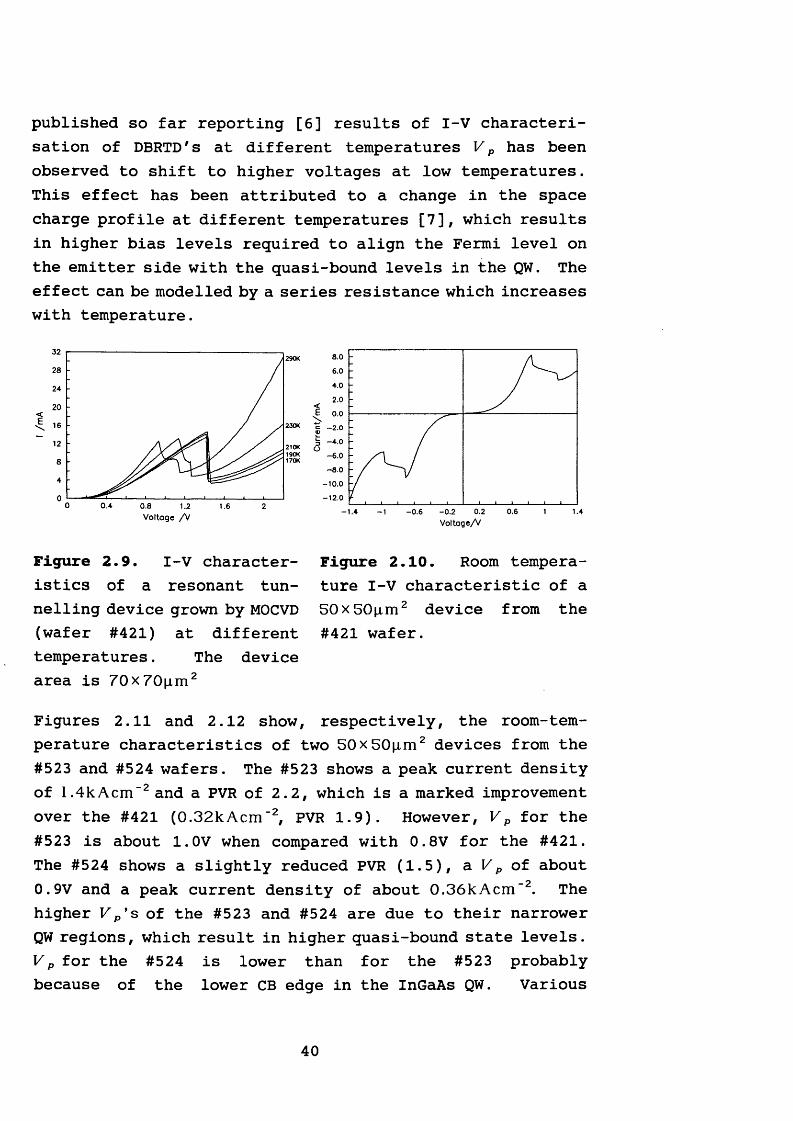
published so far reporting [6 ] results of I-V characterisation of DBRTD's at different temperatures V p has been observed to shift to higher voltages at low temperatures. This effect has been attributed to a change in the space charge profile at different temperatures [7], which results in higher bias levels required to align the Fermi level on the emitter side with the quasi-bound levels in the QW. The effect can be modelled by a series resistance which increases with temperature.
32 S.O290K
6.04.0242.0
<E 230K •2.0
- 4 . 0210K190K170K
- 6.0- 8.0
- 10.0
- 12.00 0.4 0.8 1.2 1.6 2 0.2 0.6- 0.6 - 0.2 1 1.4-1 .4 -1V o ltage /V
Figure 2.10. Room temperature I-V characteristic of a 5 0 x 5 0 n m 2 device from the #421 wafer.
Figure 2.9. I-V characteristics of a resonant tunnelling device grown by MOCVD (wafer #421) at different temperatures. The device area is 7 0 x 7 0 n m 2
Figures 2.11 and 2.12 show, respectively, the room-tem- perature characteristics of two 50x50|im2 devices from the #523 and #524 wafers. The #523 shows a peak current density of 1.4kAcm_2and a PVR of 2.2, which is a marked improvement over the #421 (0.32kAcm'2, PVR 1.9). However, V p for the #523 is about 1.0V when compared with 0.8V for the #421.The #524 shows a slightly reduced PVR (1.5), a V p of about0.9V and a peak current density of about 0.36kAcm"2. The higher K p’s of the #523 and #524 are due to their narrower QW regions, which result in higher quasi-bound state levels. V p for the #524 is lower than for the #523 probablybecause of the lower CB edge in the InGaAs QW. Various
40
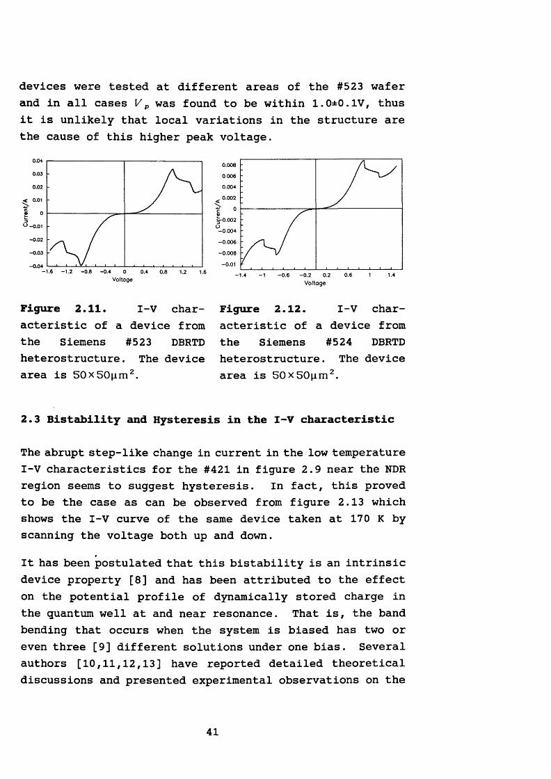
devices were tested at different areas of the #523 wafer and in all cases V p was found to be within 1.0±0.1V, thus it is unlikely that local variations in the structure are the cause of this higher peak voltage.
0.03 -
0.02 -
^ 0.01 -
« 0 - 3
° - 0.01 -
- 0.02 -
-0.03 -
-0.0+ 1--- 1--- 1—3 —i 1--- 1--- 1--- i___ i___ i___ i___ i___ i___ i-1 .6 -1 .2 -0 .8 -0 .4 0 0.4 0.8 1.2 1.6
Voltage
Figure 2.11. I-V characteristic of a device from the Siemens #523 DBRTD heterostructure. The device area is 50x50pim2.
0.008 -
0.006 -
0.004 -
^ 0.002 -
fwt-0.002 -U-0 .0 04 -
-0 .0 06 -
-0 .008 -
- 0.01 '
-1 .4 -1 -0 .6 -0 .2 0.2 0.6 1 1.4Voltage
Figure 2.12. I-V characteristic of a device from the Siemens #524 DBRTD heterostructure. The device area is 50x50pim2.
2.3 Bistability and Hysteresis in the I-V characteristic
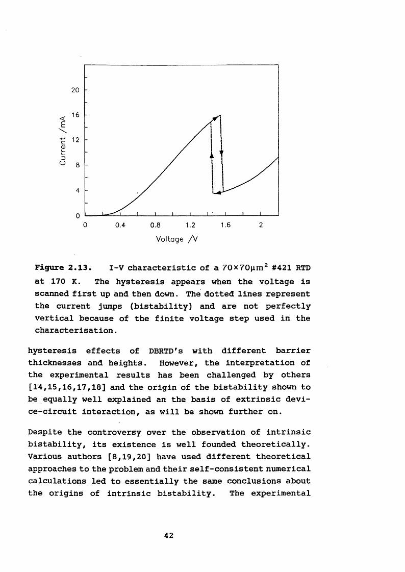
The abrupt step-like change in current in the low temperature I-V characteristics for the #421 in figure 2.9 near the NDR region seems to suggest hysteresis. In fact, this proved to be the case as can be observed from figure 2.13 which shows the I-V curve of the same device taken at 170 K by scanning the voltage both up and down.
It has been postulated that this bistability is an intrinsic device property [8 ] and has been attributed to the effect on the potential profile of dynamically stored charge in the quantum well at and near resonance. That is, the band bending that occurs when the system is biased has two or even three [9] different solutions under one bias. Several authors [10,11,12,13] have reported detailed theoretical discussions and presented experimental observations on the
41
20
<E
cCD
Do
0 1.2 1.6 20.4 0.8Voltage /V
Figure 2.13. I-V characteristic of a 7 0 x 7 0 ^ m 2 #421 RTDat 170 K. The hysteresis appears when the voltage is scanned first up and then down. The dotted lines represent the current jumps (bistability) and are not perfectly vertical because of the finite voltage step used in the characterisation.
hysteresis effects of DBRTD's with different barrier thicknesses and heights. However, the interpretation of the experimental results has been challenged by others [14,15,16,17,18] and the origin of the bistability shown to be equally well explained an the basis of extrinsic devi- ce-circuit interaction, as will be shown further on.
Despite the controversy over the observation of intrinsic bistability, its existence is well founded theoretically. Various authors [8,19,20] have used different theoretical approaches to the problem and their self-consistent numerical calculations led to essentially the same conclusions about the origins of intrinsic bistability. The experimental
42
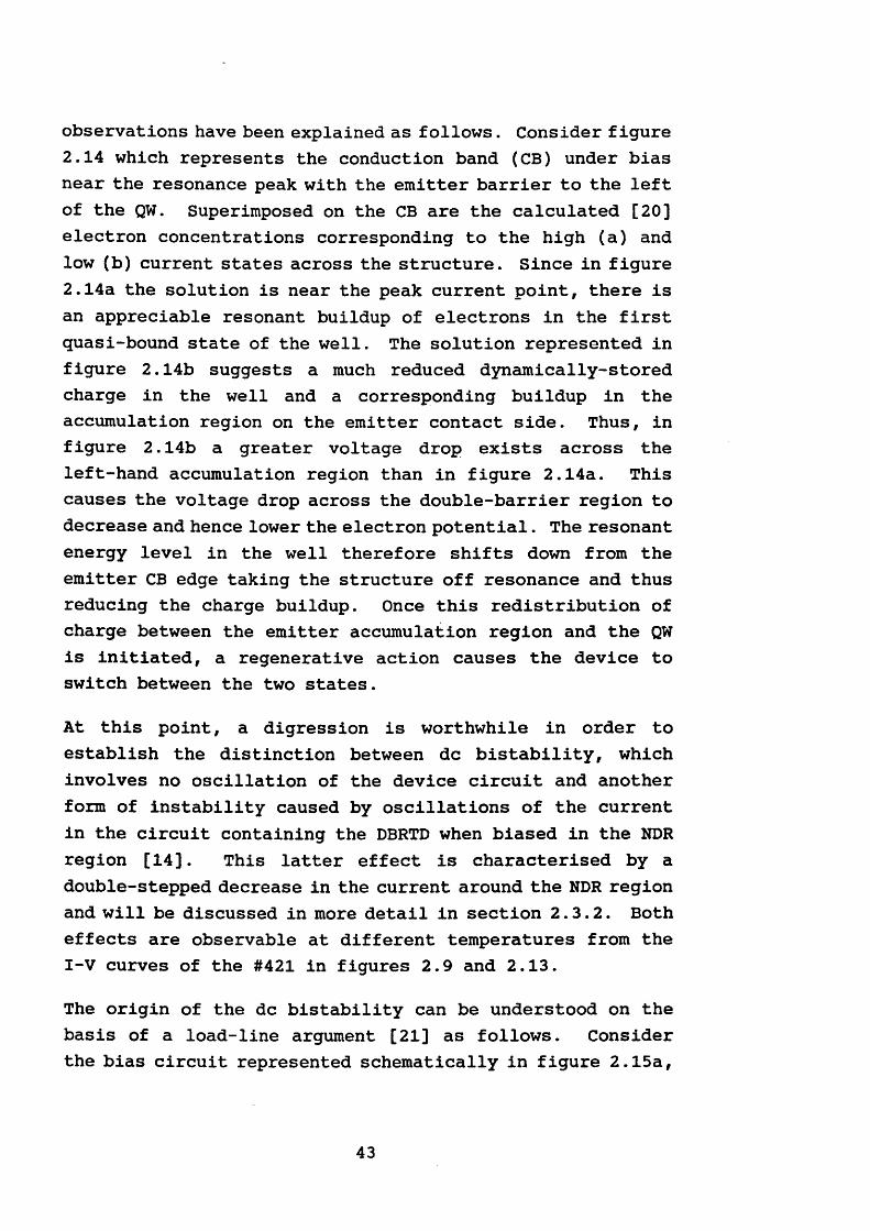
observations have been explained as follows. Consider figure 2.14 which represents the conduction band (CB) under bias near the resonance peak with the emitter barrier to the left of the QW. Superimposed on the CB are the calculated [20] electron concentrations corresponding to the high (a) and low (b) current states across the structure. Since in figure 2.14a the solution is near the peak current point, there is an appreciable resonant buildup of electrons in the first quasi-bound state of the well. The solution represented in figure 2.14b suggests a much reduced dynamically-stored charge in the well and a corresponding buildup in the accumulation region on the emitter contact side. Thus, in figure 2.14b a greater voltage drop exists across the left-hand accumulation region than in figure 2.14a. This causes the voltage drop across the double-barrier region to decrease and hence lower the electron potential. The resonant energy level in the well therefore shifts down from the emitter CB edge taking the structure off resonance and thus reducing the charge buildup. Once this redistribution of charge between the emitter accumulation region and the QW is initiated, a regenerative action causes the device to switch between the two states.
At this point, a digression is worthwhile in order to establish the distinction between dc bistability, which involves no oscillation of the device circuit and another form of instability caused by oscillations of the current in the circuit containing the DBRTD when biased in the NDR region [14]. This latter effect is characterised by a double-stepped decrease in the current around the NDR region and will be discussed in more detail in section 2.3.2. Both effects are observable at different temperatures from the I-V curves of the #421 in figures 2.9 and 2.13.
The origin of the dc bistability can be understood on the basis of a load-line argument [21] as follows. Consider the bias circuit represented schematically in figure 2.15a,
43
0.4
0.3
0.2
0.1 CB
0.0Distance
0.4
0.3EOO 0.2 OacQ>uCoa CB
0.0Distance
Figure 2.14. The conduction band of a DBRTD biased at resonance; the dotted line represents the electron concentration across the structure (a) in the high current state, and (b) in the low current state. (After Ref. [20])
where R d(V d) represents the RTD in the dc circuit as avoltage-dependent resistance (which can take on negative values) and R SI the series resistance, which here represents the sum of both the substrate and contact resistance of the RTD as well as the bias circuit resistance. V is the applied bias and I is the measured current. Assume that the I-V characteristic of the RTD has the typical shape of figure 2.15b. The device voltage V d is related to V by
V = IRS + V d (2.1)
which enables the load line shown in figure 2.15b to be constructed in order to find the stable operating point of the device. The slope of the line is -Rs and in this model is assumed independent of K d, As the applied voltage V increases, the load line moves such that it intersects the I-V curve at higher voltages. The point of intersection defines the operating point (Vd, I) of the device. Now, if R s<| R3"n I, the magnitude of the minimum value of the NDR, the intersection occurs at only one point and the whole of
44
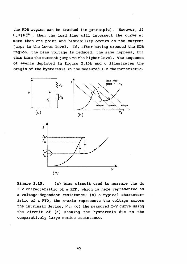
the NDR region can be tracked (in principle). However, if R 9 >|R3lln|, then the load line will intersect the curve at more than one point and bistability occurs as the current jumps to the lower level. If, after having crossed the NDR region, the bias voltage is reduced, the same happens, but this time the current jumps to the higher level. The sequence of events depicted in figure 2.15b and c illustrates the origin of the hysteresis in the measured I-V characteristic.
V(c)
Figure 2.15. (a) bias circuit used to measure the dcI-V characteristic of a RTD, which is here represented as a voltage-dependent resistance; (b) a typical characteristic of a RTD, the x-axis represents the voltage across the intrinsic device, V d; (c) the measured I-V curve using the circuit of (a) showing the hysteresis due to the comparatively large series resistance.
45
As V is increased (decreased) towards the bistable point, the current suddenly decreases (increases) from (la')to lb (Ia )» Since V is fixed by the voltage source, the drop (increase) in I has to be compensated for by an increase (drop) in V d such that equation (2.1) still holds. Thus, the measured I-V curve exhibits hysteresis.
In the case of current-oscillation induced bistability, it has been proposed [14,22] that the measured dc current may be a time-averaged ac signal when the whole measurement circuit oscillates. This oscillation has been reported to be suppressed by a capacitor connected in parallel and close to the device [10]. The persistence in this case of the bistability at low temperatures, in the absence of oscillations, was interpreted as supporting the claim for its intrinsic nature. However, as the PVR increases greatly at low temperatures through the depression of the valley current, the NDR decreases correspondingly. Hence, series resistance in the measurement circuit, including contributions from the ohmic contacts and the bulk resistance of the doping region, can still introduce hysteresis [2 2 ]. Studies performed with DBRTD's of different areas [22,23] have revealed that the bistability and hysteresis cease to exist as the device area is reduced providing that oscillations in the circuit are adequately suppressed and the (total) series resistance in the circuit is less than |R5in j*. Now, if the bistability were intrinsic, it would also be manifest in the dc characteristics of the smaller devices. However, the structures of Ref. [22] and [23] were specially designed for high NDR by using thick (72 A) AlGaAs barriers and a wide (100 A) GaAs QW. Thus, it is still possible that
1 The argument for reducing device area is that the NDR is increased roughly in proportion to the area reduction, while the intrinsic component of the series resistance, including both the alloyed ohmic contacts and bulk semiconductor away from the DB region, does not decrease proportionally to the reducing area since the whole substrate is heavily doped [14].
46
intrinsic bistability exists in structures other than these and the task still remains to distinguish experimentally between the intrinsic and extrinsic mechanisms. For electrical measurements the device is inevitably connected to external elements, whereas for optical means such as photoluminescence the signal comes from both electrons and holes [24]. In the case of magnetotunnelling experiments [10,25,26] only the density of states, rather than the density of two-dimensional electrons in the quantum well, can be obtained.
2.3.1 Stability criteria
In most theoretical predictions of power from resonant tunnelling devices [27] the device is assumed to be biased at a stable point in the NDR region. In the presence of low frequency oscillations this is not possible. Since the negative resistance of the RTD extends from dc to high frequencies it is very difficult to suppress bias circuit oscillations and as a result, most of the published characteristics, as in the case of the present study, show evidence of bias-circuit related instability. Low frequency (LF) stability is a necessary criterion for most practical applications. In mixer and detector applications, the LF oscillations can occur near the IF or video frequencies, introducing additional noise. In high-frequency oscillator operation LF bias circuit instabilities may introduce undesirable up-converted signals that modulate the carrier and noise from chaotic-like oscillation bursts [28], resulting in a signal which is unacceptable for most applications.
The following describes established stability analysis and examines the nature and origin of bias circuit oscillations as well as their effect on measured current-voltage characteristics .
47
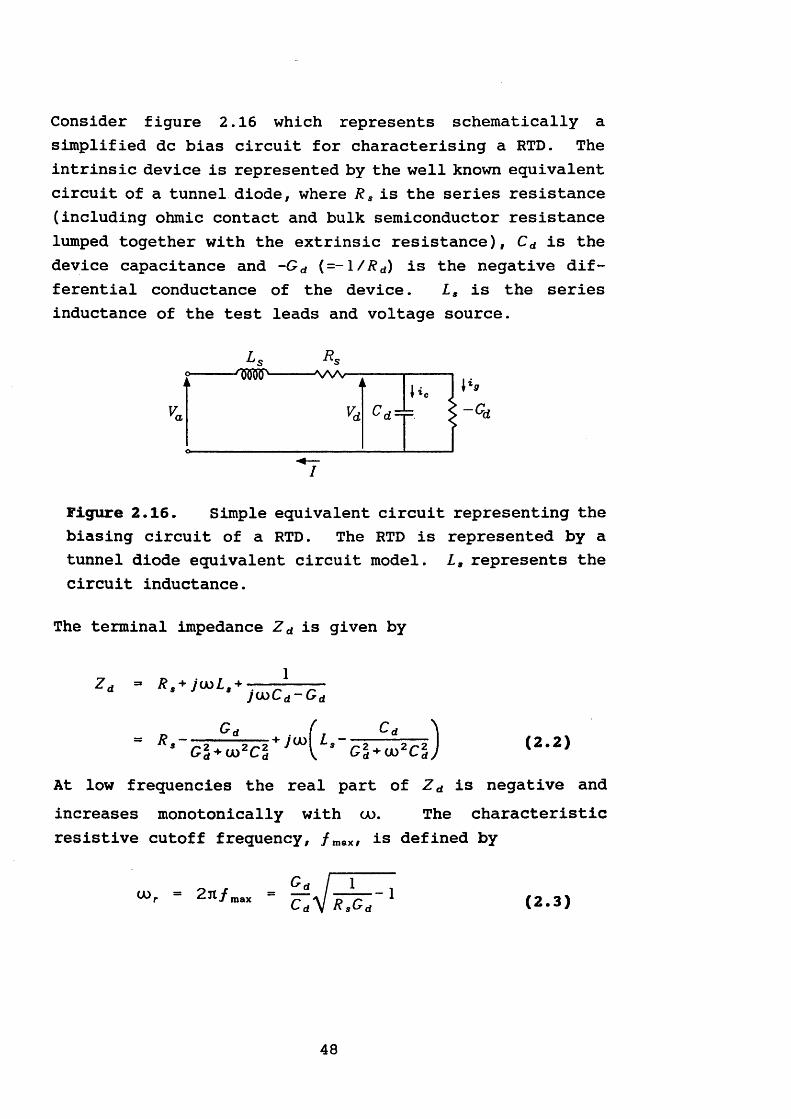
Consider figure 2.16 which represents schematically a simplified dc bias circuit for characterising a RTD. The intrinsic device is represented by the well known equivalent circuit of a tunnel diode, where R s is the series resistance (including ohmic contact and bulk semiconductor resistance lumped together with the extrinsic resistance), Cd is the device capacitance and -Gd (=-1 /Rd) is the negative differential conductance of the device. Ls is the series inductance of the test leads and voltage source.
V,a
Ls-'TOStP- AAV
Figure 2.16. Simple equivalent circuit representing the biasing circuit of a RTD. The RTD is represented by a tunnel diode equivalent circuit model. Ls represents the circuit inductance.
The terminal impedance Z d is given by
/?s + ycA)Z.,+ 1juoCd-G d
- R . ~ G5 + u>2Cd G% + w 2C? (2.2)L - d \ \* d ' \AJ \*d
At low frequencies the real part of Z d is negative andincreases monotonically with <jo. The characteristic resistive cutoff frequency, / max, is defined by
oo, = 2 it/, 1R.G,
- 1 (2.3)
48
Above this frequency, the device loses its function as an active device and thus its capacity for generating power. If R s does not include the external circuit resistance, then / max would increase correspondingly to f ri, the intrinsic negative resistance cutoff frequency [2 1 ], which can be used as a figure of merit for device comparison. Inspection of the imaginary term on the right-hand side of equation (2 .2 ) leads to the definition of / x, the internal resonance frequency of the device [2 1 ], which is obtained by setting the imaginary part of Z d to zero:
o x n ^= 2n/‘ = V ^ ' ^ i (2-4)
The subsequent analysis will show the importance of the parameter /*, which should be larger than / max to prevent oscillations [29].
The dc stability criterion has been established in the previous section using the load-line concept. The basic requirement for a RTD biased at the minimum NDR point is therefore
R,Gd < 1 ( 2 . 5 )
Let us now assume that the RTD is biased at this point, where the voltage across -Gd is V d, and that over a small voltage range about V d the I-V curve is linear. Then, the differential equation representing the circuit of figure 2.16 is
d 2K rf dV,V - L.C*-^T+iR.C<-L,Gd-)-^+Vd{\-R.Gd) (2>6)
For small signals, equation (2.6) is linear since both G dand Cd have been assumed independent of small changes in V d. In this case, the general solution of (2 .6 ) has the form
49
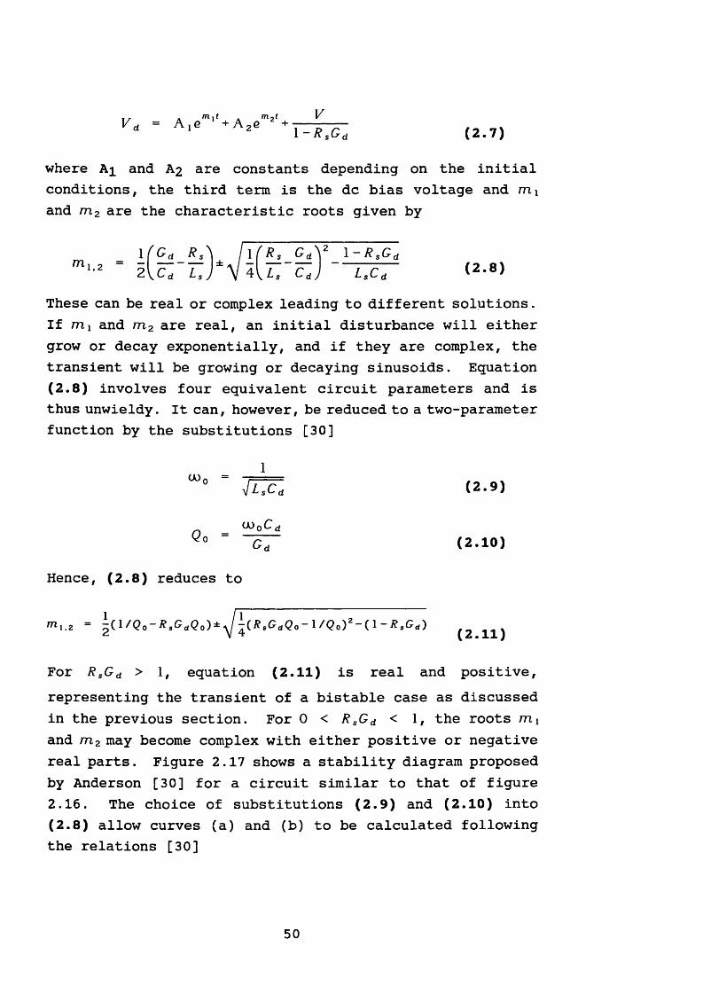
j r a TTl \t TTljt " V
K “ ■ A ‘e + A ‘e T T ^ d (2.7)
where A^ and A 2 are constants depending on the initial conditions, the third term is the dc bias voltage and m^ and m 2 are the characteristic roots given by
m>'2 2 U d L j ± yj 4\L, C j L,Cd (2 -8 )These can be real or complex leading to different solutions. If rrtx and m 2 are real, an initial disturbance will either grow or decay exponentially, and if they are complex, the transient will be growing or decaying sinusoids. Equation(2 .8 ) involves four equivalent circuit parameters and is thus unwieldy. It can, however, be reduced to a two-parameter function by the substitutions [30]
if R s Gd}2 1 — R sG d
1
Qo =
Hence, (2.8) reduces to
(2-9)
u>0 CdGd (2.10)
For RsG d > 1, equation (2.11) is real and positive,representing the transient of a bistable case as discussed in the previous section. For 0 < R sG d < 1, the roots mi and m 2 may become complex with either positive or negative real parts. Figure 2.17 shows a stability diagram proposed by Anderson [30] for a circuit similar to that of figure 2.16. The choice of substitutions (2.9) and (2.10) into(2 .8 ) allow curves (a) and (b) to be calculated following the relations [30]
50
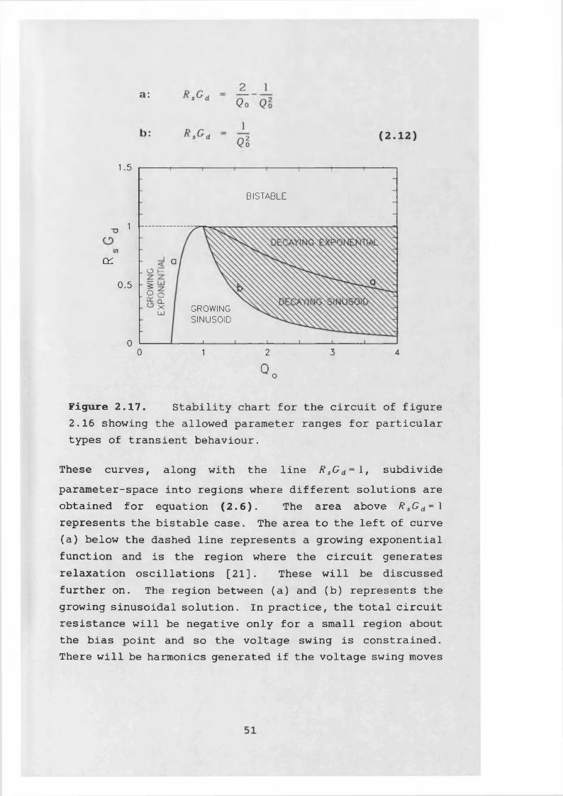
1.5
BISTABLE
1
QL_ o i-
0.5 .goXLd GROWING
SINUSOID
00 2 3 41
Q o
Figure 2.17. Stability chart for the circuit of figure 2.16 showing the allowed parameter ranges for particular types of transient behaviour.
These curves, along with the line R sGd = \ , subdivideparameter-space into regions where different solutions are obtained for equation (2.6). The area above R sGd = 1represents the bistable case. The area to the left of curve(a) below the dashed line represents a growing exponential function and is the region where the circuit generates relaxation oscillations [21]. These will be discussedfurther on. The region between (a) and (b) represents the growing sinusoidal solution. In practice, the total circuit resistance will be negative only for a small region about the bias point and so the voltage swing is constrained. There will be harmonics generated if the voltage swing moves

significantly out of the linear region. Hence, steady sinusoidal oscillations can only be obtained if R s is close to (but less than) 1/Gd.
The hatched area between (b) and (a) represents the decaying sinusoidal solutions and the remaining part above (a) represents the decaying exponential region. With circuit parameter values within these areas, the device is stable and it would thus be theoretically possible to measure the stable I-V characteristic.
From (2.11) and (2.12) we can quantify the circuit conditions which lead to the various regions of figure 2.17. For growing exponential solutions (2 .1 1 ) must be real and mi and/or m 2 must be positive. Thus, (2.11) and (2.12) give the conditions
(2.13a)Qo Qo
R s^d < — ~1 G\l,Ql Cd (2.13b)
For decaying exponentials, (2.13a) still holds but both m x and m 2 must be negative and hence,
0\lsRsGd * Cd (2.14)
Growing sinusoidal solutions require (2.11) to be complex with a positive real part. Thus (2.11) and (2.12) give
Qo Qo (2.15a)
1 G\L,Q o (2.15b)
And for decaying sinusoids, (2.15a) holds but (2.11) must have a negative real part, so that
52
G dLsR.G, > C d (2.16)
Thus the stable regions of figure 2.17 (hatched areas) can be characterised by considering (2.14) and (2.16) together with (2.5) to give the stability criteria for the circuit of figure 2.16 as
0\L,< R*Gd K 1 (2.17)
From the inequality (2.17) and the expressions for cor andca) * of (2.3) and (2.4), it may be shown that for stability oor < go* [21,29] .
Now, for a given device, G d and Cd are intrinsic properties,as is the part of R s (in figure 2.16) which combines the ohmic contact and bulk semiconductor resistance. Thus, the stability criterion (2.17) reduces to
i < £-G\ (2.18)
The foregoing analysis applies for other voltage-controlled negative conductance devices which exhibit NDC from dc to high frequencies, such as tunnel diodes and Gunn devices. For tunnel diodes, minimising lead inductance is a problem. However, it is relatively simpler to stabilise a tunnel diode than a RTD because the former has a larger capacitance. Gunn devices, on the other hand, have a much smaller negative conductance at the operating point which makes stabilisation easier to achieve.
With the DBRTD's studied in chapters 4 and 5, typical values of G d and Cd are of the order of millisiemens and picofarads respectively. This constrains Ls to nanohenries and even smaller. Thus, conventional microwave packaging may just be sufficient to introduce dc instability. Smaller devices,
53
with correspondingly lower G d values, could be potentiallystable providing the equivalent bias circuit inductance and capacitance are adjusted to satisfy (2.18). Devices with considerably higher peak current densities and PVR's, suitable for high frequency applications, would have reduced areas. However lower values of Cd and relatively higher G d place even more severe restrictions on LSf which would preclude the use of conventional microwave packaging. Whisker contacting techniques could reduce Ls significantly, although in some cases not enough. Another possible method would be to mount the device between the plates of a capacitor, as is effectively the case with resonant cap circuits [31,32] which have been used successfully for millimetre-wave IMPATT oscillators. In this case, however, added capacitance inside the microwave circuit will lower the effective cutoff frequency and output power [29] especially since RTD's have a relatively low impedance.
2.3.2 Observation and Simulation of bias circuit oscillations and extrinsic bistability
The purpose of the numerical simulations to be described here is to study the effect on the I-V characteristics of external elements in the biasing circuit and to obtain a physical picture of the interaction of the RTD with the latter. Several studies [15,16,17,18] have reported numerical simulations of extrinsic instability effects on the I-V characteristics of DBRTD's which are similar to experimentally observed curves, employing methods initially applied for tunnel diodes [33]. A similar approach will be adopted here.
For the purpose of the calculation, the circuit of figure 2.16 is modified to that of figure 2.18, where the intrinsic device is now simply a nonlinear (voltage-controlled) conductance, G d(K). The resistance R represents the total
54
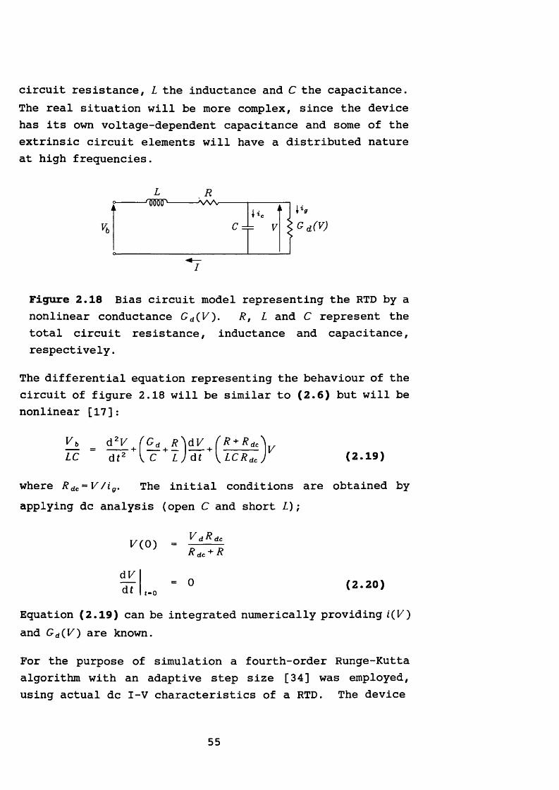
circuit resistance, L the inductance and C the capacitance. The real situation will be more complex, since the device has its own voltage-dependent capacitance and some of the extrinsic circuit elements will have a distributed nature at high frequencies.
w v
Figure 2.18 Bias circuit model representing the RTD by a nonlinear conductance G d(V'). R, L and C represent the total circuit resistance, inductance and capacitance, respectively.
The differential equation representing the behaviour of the circuit of figure 2.18 will be similar to (2 .6 ) but will be nonlinear [17]:
Vjb _ d zK [ (Gd | /? W t f R + Rdc\ LC df2 A C + LJ dt+\LCRdc) (2.19)
where Rdc^V/ig. The initial conditions are obtained by applying dc analysis (open C and short L);
K( 0 ) = V dc
dV d t t-o
R d c + R
= 0 (2.20)Equation (2.19) can be integrated numerically providing i(V) and G d(V) are known.
For the purpose of simulation a fourth-order Runge-Kutta algorithm with an adaptive step size [34] was employed, using actual dc I-V characteristics of a RTD. The device
55
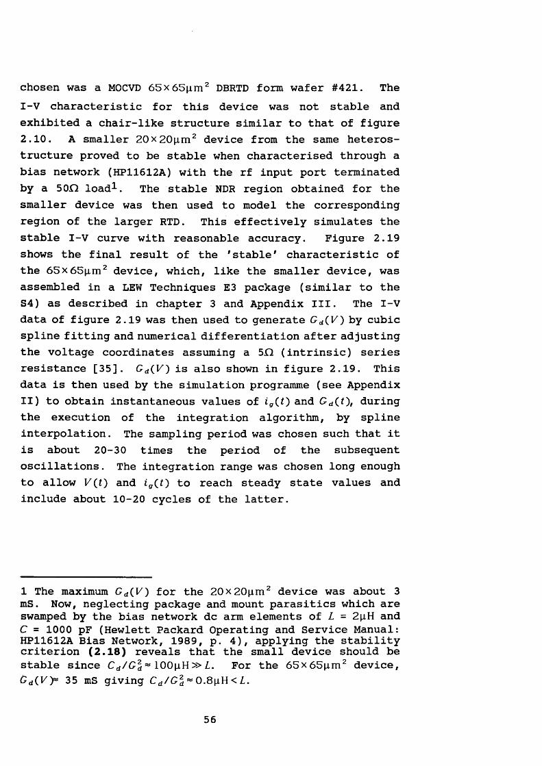
chosen was a MOCVD 6 5 x 6 5 ^ m 2 DBRTD form wafer #421. The I-V characteristic for this device was not stable and exhibited a chair-like structure similar to that of figure 2.10. A smaller 20x20p,m2 device from the same heterostructure proved to be stable when characterised through a bias network (HP11612A) with the rf input port terminated by a 50D load^. The stable NDR region obtained for the smaller device was then used to model the corresponding region of the larger RTD. This effectively simulates the stable I-V curve with reasonable accuracy. Figure 2.19 shows the final result of the 'stable' characteristic of the 65x65|im2 device, which, like the smaller device, was assembled in a LEW Techniques E3 package (similar to the S4) as described in chapter 3 and Appendix III. The I-V data of figure 2.19 was then used to generate G dQV) by cubic spline fitting and numerical differentiation after adjusting the voltage coordinates assuming a 5.Q (intrinsic) series resistance [35]. C d(K) is also shown in figure 2.19. This data is then used by the simulation programme (see Appendix II) to obtain instantaneous values of ig(0 and £ d(0/ during the execution of the integration algorithm, by spline interpolation. The sampling period was chosen such that it is about 20-30 times the period of the subsequent oscillations. The integration range was chosen long enough to allow K(£) and ig ( 0 to reach steady state values and include about 1 0 - 2 0 cycles of the latter.
1 The maximum G d{V) for the 20x20pim2 device was about 3 mS. Now, neglecting package and mount parasitics which are swamped by the bias network dc arm elements of L = 2piH and C = 1000 pF (Hewlett Packard Operating and Service Manual: HP11612A Bias Network, 1989, p. 4), applying the stability criterion (2.18) reveals that the small device should bestable since Cd/Gd * 100p,H » L. For the 6 5 x 6 5 n m 2 device, Gdi^y* 35 mS giving Cd/Gd » 0.8piH < L.
56
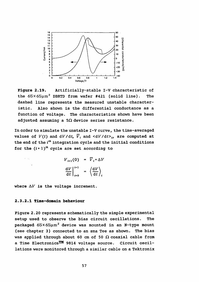
-400 0.2 0.4 0.6 0.8V o lta g e /V
1.2 1.4
Figure 2.19. Artificially-stable I-V characteristic of the 6 5 x 6 5 n m 2 DBRTD from wafer #421 (solid line). The dashed line represents the measured unstable characteristic. Also shown is the differential conductance as a function of voltage. The characteristics shown have been adjusted assuming a 5D device series resistance.
In order to simulate the unstable I-V curve, the time-averaged values of V(t) and dV/dt, V t and <dV/dt>u are computed at the end of the ith integration cycle and the initial conditions for the (*+l)t/l cycle are set according to
where AV is the voltage increment.
2.3.2.1 Time-domain behaviour
Figure 2.20 represents schematically the simple experimental setup used to observe the bias circuit oscillations. The packaged 65 x 6 5 p m 2 device was mounted in an N-type mount (see chapter 3) connected to an sma Tee as shown. The bias was applied through about 60 cm of 50 D coaxial cable from a Time Electronics™ 9814 voltage source. Circuit oscillations were monitored through a similar cable on a Tektronix
57
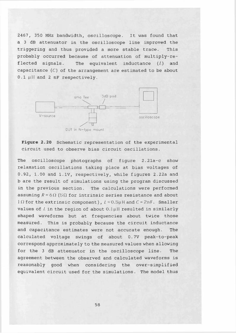
2467, 350 MHz bandwidth, oscilloscope. It was found that a 3 dB attenuator in the oscilloscope line improved the triggering and thus provided a more stable trace. This probably occurred because of attenuation of multiply-reflected signals. The equivalent inductance (I) and capacitance (C) of the arrangement are estimated to be about 0.1 |iH and 2 nF respectively.
3dB padsm a Tee
V -s o u rc e o sc illo sco p e
DUT in N—type m o u n t
Figure 2.20 Schematic representation of the experimental circuit used to observe bias circuit oscillations.
The oscilloscope photographs of figure 2.21a-c show relaxation oscillations taking place at bias voltages of 0.92, 1.00 and 1.1V, respectively, while figures 2.22a and b are the result of simulations using the program discussed in the previous section. The calculations were performed assuming R = 6Cl (5D for intrinsic series resistance and about 1 D for the extrinsic component), L = 0.5|j.H and C = 2nF. Smaller values of L in the region of about 0.1 [lU resulted in similarly shaped waveforms but at frequencies about twice those measured. This is probably because the circuit inductance and capacitance estimates were not accurate enough. The calculated voltage swings of about 0.7V peak-to-peak correspond approximately to the measured values when allowing for the 3 dB attenuator in the oscilloscope line. The agreement between the observed and calculated waveforms is reasonably good when considering the over-simplified equivalent circuit used for the simulations. The model thus
58

represents the actual situation fairly well and should therefore allow useful qualitative (if not quantitative) information about circuit behaviour to be extracted.
Figures 2.23-2.26 give the results of simulations carried out with circuit parameters and bias voltages listed in table 2.2. In the case of figure 2.22 the initial circuit conditions are such that (2.15a) and (2.15b) are satisfied such that the transient is a growing sinusoid.
59
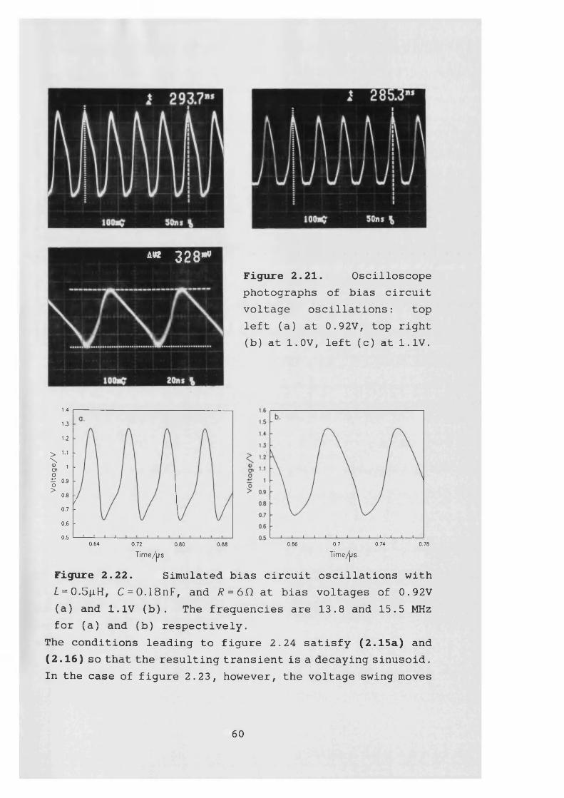
4« 3 2 8 - *Figure 2.21. Oscilloscope photographs of bias circuit voltage oscillations: topleft (a) at 0.92V, top right (b) at 1.0V, left (c) at 1.1V.
1.4
u 1.2
> 11 \«) !O)otL 0.9 o> 0.8
0.7
0.6 0.5
0.64 0.72 0.80 0.88 0.66 0.7 0.74 0.78
Time/ps Time/ps
Figure 2.22. Simulated bias circuit oscillations with f = 0.5jiH, C = 0.18nF, and R = 6D. at bias voltages of 0.92V (a) and 1.IV (b). The frequencies are 13.8 and 15.5 MHz for (a) and (b) respectively.
The conditions leading to figure 2.24 satisfy (2.15a) and (2.16) so that the resulting transient is a decaying sinusoid. In the case of figure 2.23, however, the voltage swing moves
6 0
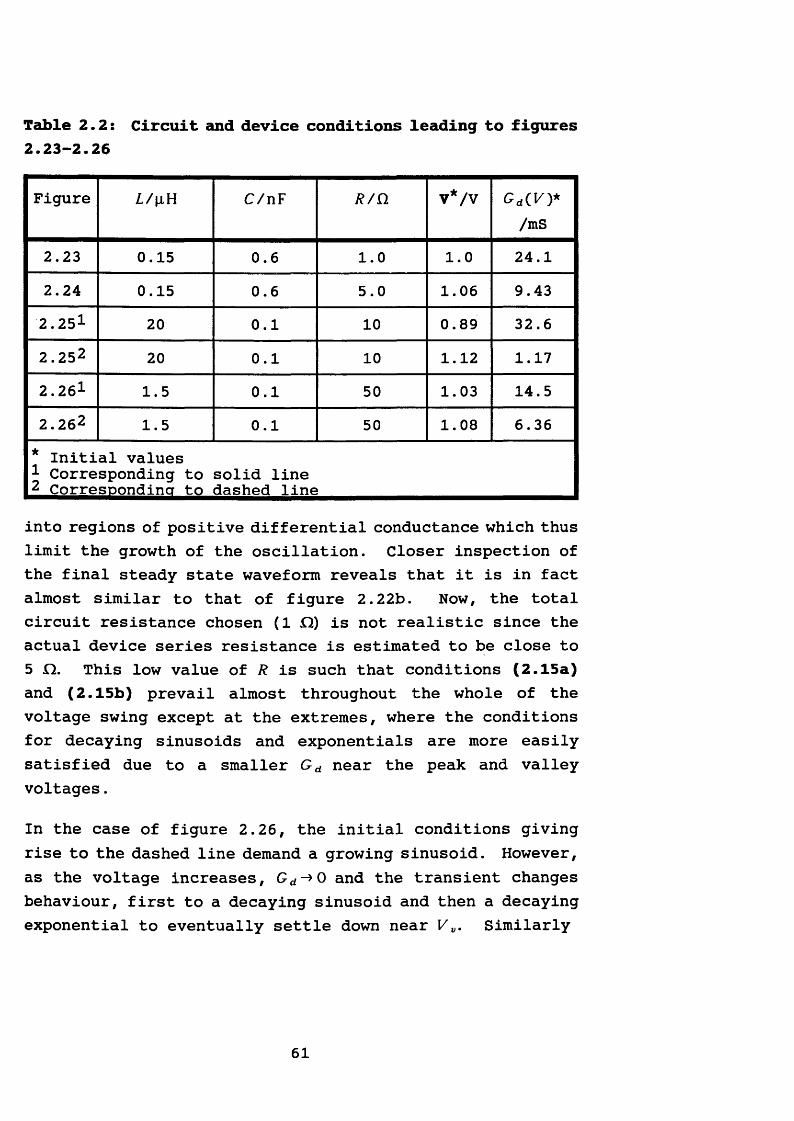
Table 2.2: Circuit and device conditions leading to figures 2.23-2.26
Figure L/[lH C/nF R/Q V*/V O d(V)*/mS
2.23 0.15 0 . 6 1 . 0 1 . 0 24.12.24 0.15 0 . 6 5.0 1.06 9.432.251 2 0 0 . 1 1 0 0.89 32.62.252 2 0 0 . 1 1 0 1 . 1 2 1.172.261 1.5 0 . 1 50 1.03 14.52.262 1.5 0 . 1 50 1.08 6.36* Initial values1 Corresponding to solid line2 CorresDondina to dashed line
into regions of positive differential conductance which thus limit the growth of the oscillation. Closer inspection of the final steady state waveform reveals that it is in fact almost similar to that of figure 2.22b. Now, the total circuit resistance chosen ( 1 II) is not realistic since the actual device series resistance is estimated to be close to 5 Q. This low value of R is such that conditions (2.15a) and (2.15b) prevail almost throughout the whole of the voltage swing except at the extremes, where the conditions for decaying sinusoids and exponentials are more easily satisfied due to a smaller G d near the peak and valley voltages.
In the case of figure 2.26, the initial conditions giving rise to the dashed line demand a growing sinusoid. However, as the voltage increases, G d->0 and the transient changes behaviour, first to a decaying sinusoid and then a decaying exponential to eventually settle down near V v. Similarly
61
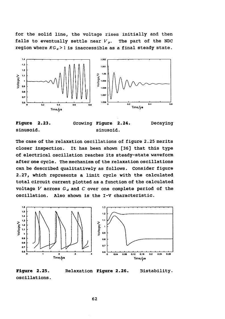
for the solid line, the voltage rises initially and then falls to eventually settle near V p. The part of the NDC region where R G d > 1 is inaccessible as a final steady state.
1.4
1.3 -
1.2
< 11
0.8
0.7
0.6 0 0J 0.4 0.6 0.8
1.062
1.061
^ 1.06
O>1.058
1.057
1.0560.4 0.60.20
Time/psTime/ps
Figure 2.23.sinusoid.
Growing Figure 2.24, sinusoid.
Decaying
The case of the relaxation oscillations of figure 2.25 merits closer inspection. It has been shown [36] that this type of electrical oscillation reaches its steady-state waveform after one cycle. The mechanism of the relaxation oscillations can be described qualitatively as follows. Consider figure 2.27, which represents a limit cycle with the calculated total circuit current plotted as a function of the calculated voltage V across G d and C over one complete period of the oscillation. Also shown is the I-V characteristic.
1.6
1.4
1.3
< 1.24>o>3
0.9
0.80.7
0.6 0 1 2 3 4Timers
Figure 2.25. Relaxationoscillations.
1.3
1.2
O 0.9
0.8
0.7
0.60.24 0.280.04 0.08 0.12 0.16 0.20
Time/jjs
Figure 2.26. Bistability.
62
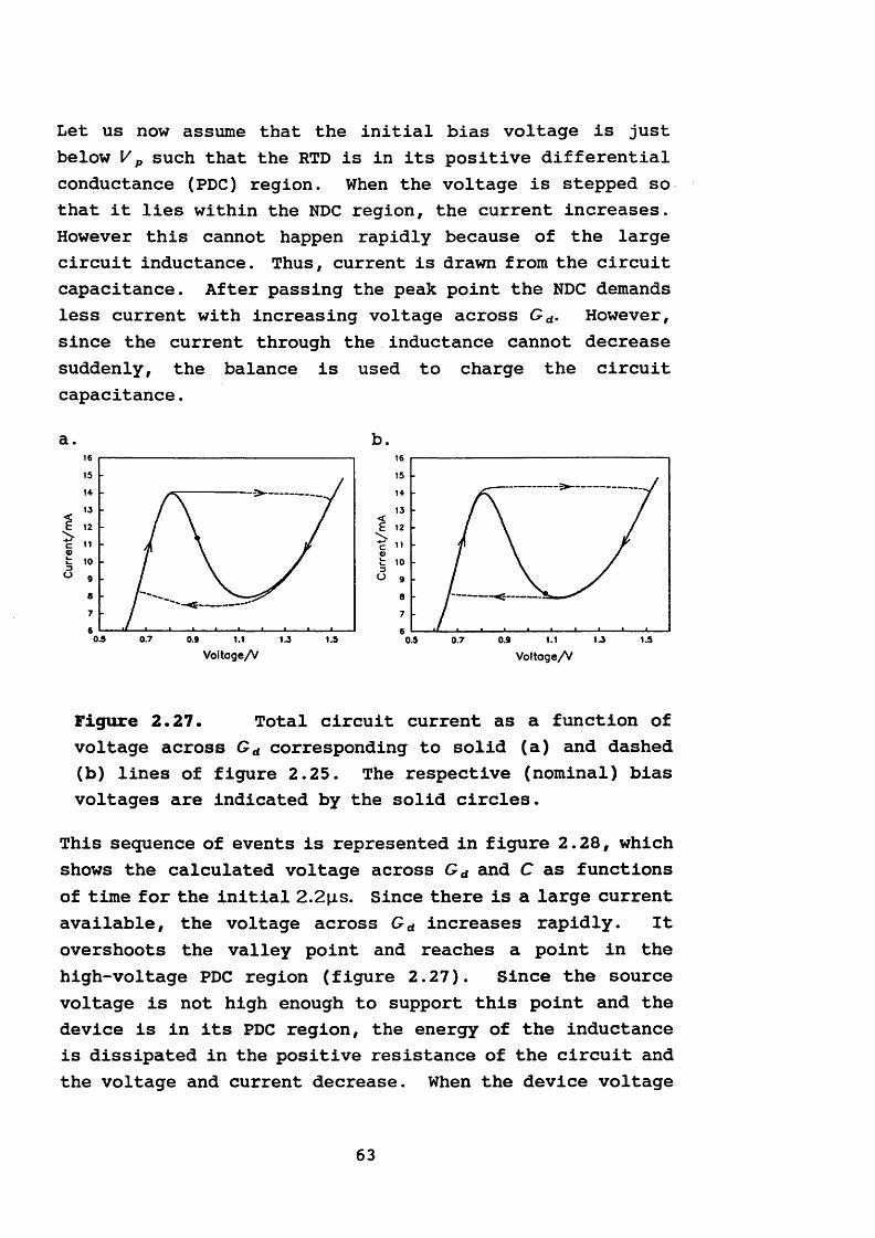
Let us now assume that the initial bias voltage is just below V p such that the RTD is in its positive differential conductance (PDC) region. When the voltage is stepped so that it lies within the NDC region, the current increases. However this cannot happen rapidly because of the large circuit inductance. Thus, current is drawn from the circuit capacitance. After passing the peak point the NDC demands less current with increasing voltage across G d. However, since the current through the inductance cannot decrease suddenly, the balance is used to charge the circuit capacitance.
a. b.161514 -> -------
1312
1110
9
876 0.7 0.9 1.1 1.5
15 -
1ca>3o
1.50.5 0.9 1.10.7
Voltage/V VoltogeA
Figure 2.27. Total circuit current as a function of voltage across G d corresponding to solid (a) and dashed (b) lines of figure 2.25. The respective (nominal) bias voltages are indicated by the solid circles.
This sequence of events is represented in figure 2.28, which shows the calculated voltage across G d and C as functions of time for the initial 2.2p.s. Since there is a large current available, the voltage across G d increases rapidly. It overshoots the valley point and reaches a point in the high-voltage PDC region (figure 2.27). Since the source voltage is not high enough to support this point and the device is in its PDC region, the energy of the inductance is dissipated in the positive resistance of the circuit and the voltage and current decrease. When the device voltage
63
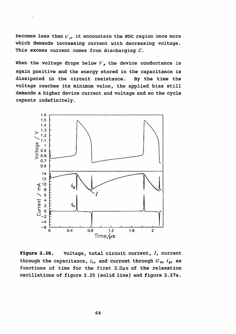
becomes less than y v, it encounters the NDC region once more which demands increasing current with decreasing voltage. This excess current comes from discharging C.
When the voltage drops below V p the device conductance isagain positive and the energy stored in the capacitance is dissipated in the circuit resistance. By the time the voltage reaches its minimum value, the applied bias still demands a higher device current and voltage and so the cycle repeats indefinitely.
1.61.51.4
> 1 3 1.2
^ 1.1& 13 0.9o 0.8
0.70.614 12
< 10 £ 8 \ 6c ^<D o
z-
3 0o -2-4-6
0 0.4 0.8 1.2 1.6 2Time/pis
Figure 2.28. Voltage, total circuit current, /, current through the capacitance, ic, and current through G d, ig, as functions of time for the first 2 .2 p.s of the relaxation oscillations of figure 2.25 (solid line) and figure 2.27a.
64
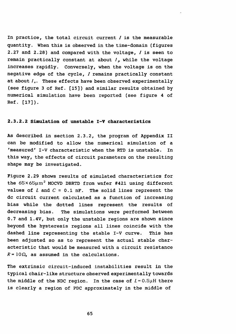
In practice, the total circuit current I is the measurable quantity. When this is observed in the time-domain (figures 2.27 and 2.28) and compared with the voltage, I is seen to remain practically constant at about Ip while the voltage increases rapidly. Conversely, when the voltage is on the negative edge of the cycle, / remains practically constant at about /„. These effects have been observed experimentally (see figure 3 of Ref. [15]) and similar results obtained by numerical simulation have been reported (see figure 4 of Ref. [17]).
2.3.2.2 Simulation of unstable I-V characteristics
As described in section 2.3.2, the program of Appendix II can be modified to allow the numerical simulation of a 'measured' I-V characteristic when the RTD is unstable. In this way, the effects of circuit parameters on the resulting shape may be investigated.
Figure 2.29 shows results of simulated characteristics for the 6 5 x 6 5 n m 2 MOCVD DBRTD from wafer #421 using different values of L and C = 0.1 nF. The solid lines represent the dc circuit current calculated as a function of increasing bias while the dotted lines represent the results of decreasing bias. The simulations were performed between0.7 and 1.4V, but only the unstable regions are shown since beyond the hysteresis regions all lines coincide with the dashed line representing the stable I-V curve. This has been adjusted so as to represent the actual stable characteristic that would be measured with a circuit resistance R= IOC, as assumed in the calculations.
The extrinsic circuit-induced instabilities result in the typical chair-like structure observed experimentally towards the middle of the NDC region. In the case of Z = 0.5piH there is clearly a region of PDC approximately in the middle of
65
15L{ pH):
x 5.0+ 0.5o 0.1
7
bias increasing bias decreasing
60.8 1.2 1.4
Bias voltage/V
Figure 2.29 Simulated unstable dc characteristics of the 6 5 x 6 5 ^ m 2 MOCVD DBRTD from wafer #421 using different values of L, C = 0.1 nF and R = 10H. The bias voltage was increased (solid lines) and then decreased (dotted lines) by 0.01V increments in the calculation. The dashed line represents the 'measured' characteristic if the circuit were to be stable. Most of the point-labels have been removed from the central and peripheral regions for clarity.
the plateau. It is observed that the width of the hysteresis loops depends mainly on the relative values of L and C, and that around V p the loops are narrower than the corresponding loops near V v.
These effects may be explained as follows. For small L the prevailing circuit conditions with the device biased near the unstable region are those which support decaying sinusoids near V p and V v (to a greater extent near V v because of the slower change in £ d(K) in this vicinity) hence the circuit remains stable to within the extremities of the NDC region. When the bias reaches the middle region where RGd < G dL / C , the circuit starts oscillating almost sinusoidally since with the maximum G d of about 35 mS condition
66
(2.15a) is satisfied which implies growing sinusoids. The amplitude is limited as mentioned earlier, and steady-state waveforms are established and the dc circuit measures the time average of the circuit current. Now, for Z = 0.5p.H and higher, conditions (2.13a) and (2.13b) are upheld for bias voltages within the middle of the NDC region. The resulting exponentially-growing voltage is then limited as described in the previous section, giving rise to relaxation oscillations. Thus it is the larger values of L/C that cause the circuit to become unstable at voltages relatively closer to the PDC sections and to quickly move into regions where (2.13a) and (2.13b) are satisfied, explaining the sharp demarcation between stable and unstable regions for higher L. It can therefore be appreciated that, in addition to defining the stability range for given circuit parameters, the shape of G d(K) controls the symmetry of the hysteresis loops near V p and V v. Thus, because of the steeper variation of G d(K) near V p, the damping due to oscillatory excursions into the PDC region increases faster and oscillations cease sooner, resulting in a narrow loop in this vicinity. Near the valley, however, C d(V) varies more slowly, and oscillation is permitted at bias voltages closer to V v. As a matter of fact, inspection of figure 2.25 reveals that the oscillation represented by the dashed line at a bias close to V v has about 63% duty cycle as opposed to about 21% for the other oscillation (solid line). The frequency also increases slightly, as is observed from figures 2.25 and 2 .2 1 .
The extent to which oscillations are allowed to persist past V v depends on whether the bias is increasing (i.e. G d(K) increasing) or decreasing (Cd(K) decreasing) since the initial conditions at any bias voltage are determined by the steady-state conditions at the previous voltage.
67
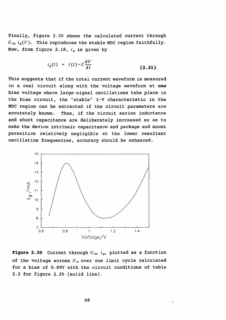
Finally, figure 2.30 shows the calculated current through Gd§ ig{Y)• This reproduces the stable NDC region faithfully. Now, from figure 2.18, ig is given by
< „ ( 0 - (2.21)This suggests that if the total current waveform is measured in a real circuit along with the voltage waveform at one bias voltage where large-signal oscillations take place in the bias circuit, the 'stable' I-V characteristic in the NDC region can be extracted if the circuit parameters are accurately known. Thus, if the circuit series inductance and shunt capacitance are deliberately increased so as to make the device intrinsic capacitance and package and mount parasitics relatively negligible at the lower resultant oscillation frequencies, accuracy should be enhanced.
<
15
14
13
12
1 1
10
9
8
70 .5 1.41.20.8 1
Voltage/V
Figure 2.30 Current through G dt ig, plotted as a functionof the voltage across G d over one limit cycle calculated for a bias of 0.89V with the circuit conditions of table 2.2 for figure 2.25 (solid line).
68
2.4 Implications of dc stability criteria on rf power generation
It has been mentioned previously that bias circuit instabilities adversely affect the applicability of RTD's. Since the usefulness of these devices will be determined by functionality rather than interesting physics, it would be fruitful to assess the effects of stability criteria on power generation.
Condition (2.18) would require LsG d/Cd< 1 in the rf sectionof a potential oscillator circuit. Assuming G d and Cd scale linearly with device area, A, and writing these as the respective conductance and capacitance per unit area, this inequality can be re-written as
G d is an intrinsic property of the device structure and can only be partially controlled by device design.
It is apparent that stability will be improved by reducing device area, which is consistent with requirements for high frequency devices. Reducing A results in smaller capacitance, which is beneficial in coupling these low-impedance devices to an rf load. However (2.22) also implies that the device capacitance should be increased to improve dc stability. This is in direct conflict with performance criteria for high-frequency devices [37]
The output power from a RTD may be calculated by assuming that the device is matched to a circuit with a load resistance R L. Thus, from (2.2)
< 1 (2.22)
G DR l = -R s + A C| + (ooCD)2 (2.23)
69
where the conductance and capacitance per unit area have been used instead of G d and Cd, since the power scales with device area and thus A has to be selected. In order to examine the effects of G D and C D on power generation, let us assume A to be unit area and R s to be negligibly small. Under these conditions (2.23) reduces to
where V r/ is the rf voltage amplitude across the RTD. Letus further assume G D to be constant over the NDC region and the bias such that V rf reaches V p and V v during the cycle. Thus V rf will be assumed as (Vv - K p)/2 = AK/2 and ^ = (^p'^)/AK, where J p and J v are the peak and valley current densities, respectively. With these assumptions, P rf at very high frequencies reduces to
This has encouraged efforts to increase J p and decrease C D,while maintaining a reasonably high PVR, in a bid to raise power output at high frequencies. If stability is considered, however, the analysis is not strictly valid except for the ideal situation with negligible Ls. Condition (2.22) must therefore be applied, which, for unit area, requires C D > G\LS. This imposes a lower bound on device intrinsic capacitance which is determined by G D apart from Ls. It is therefore
G D
G | + ( ( A ) C d)2 (2.24)
The power generated by a RTD of unit area is thus
1 W r f\22 R l
1 W rf\Z
(2.25)
(2.26)
70
obvious that A K cannot be ignored when designing devices for high frequency power generation, since the stability-limited power becomes1 [29]
P rf < - A K A J - — ^ = -(AK)r/ _ s^ y j AJL' {2.21)
Where the device properties are concerned, the requirements for stability are therefore in direct conflict with those for high frequency power generation. When the device is limited by stability, the performance becomes related to the ratio A JLS/CD. Stability considerations will not limit the output power of a device only if the maximum power from(2.27) exceeds the power from (2.26).
Finally, the circuit parameters limiting dc-stable rf generation are the load resistance and the lead inductance. R l has to be small for improved matching since RTD's have a relatively low impedance. This limits the usable device area through (2.5) especially for high frequencies. The minimum value of Ls necessary to prevent bias circuit oscillations limits the device area through (2.23).
1 Prf = | V rfl*rf | /2. Because \Vrf\ has been assumed to be (Kp-K„)/2 = AK/2, then 11 rf |-(/p - /„)/2 - A( Jp - Jv)/2 - A A J/2. Thus Prf = A A F A J / 8 .
71
References1. T. P. E. Broekaert, W. Lee, and C. G. Fonstad, "Pseu- domorphic Ino.5 3 Gao.4 7 As/AlAs/InAs resonant tunneling diodes with peak-to-valley current ratios of 30 at room temperature", Appl. Phys. Lett., Vol. 53, 1988, pp. 1545-1547.2. A. Wright, Private communication3. C. I. Huang, M. J. Paulus, C. A. Bozada, S. C. Dudley, K. R. Evans, C. E. Stutz, R. L. Jones, and M. E. Cheney, "AlGaAs/GaAs double barrier diodes with high peak-to-valley current ratio", Appl. Phys.f Lett., Vol. 51, 1987, pp. 121-123.4. R. D. Schnell, H. Tews, and R. Neumann, "Room-temperature operation of AlGas/GaAs resonant tunnelling structures grown by metalorganic vapour-phase epitaxy," Electron. Lett., Vol. 25, 1989, pp. 830-831.5. J. Wilier, D. Ristow, W. Kellner, and H. Oppolzer, "Very stable Ge/Au/Cr/Au ohmic contacts to GaAs," J. Electrochem. Soc., Vol. 135, pp. 179-181, 1988.6 . The literature abounds with such reports. To name but a few, see for example: C. I. Huang, et al., Appl. Phys. Lett., Vol. 51, 1987, pp. 121-123;C. R. Wei and Y. W. Choi, ibid., Vol. 58, 1991, pp. 1077-1079; J. Chen et al., J. Appl. Phys., Vol. 70, 1991, pp. 3131-3136, etc.7. J. Chen, J. G. Chen, C. H. Yang, and R. A. Wilson, "The I-V characteristics of double-barrier resonant tunneling diodes: observation and calculation on their temperature dependence and asymmetry," J. Appl. Phys., Vol. 70, pp. 3131-3136, 1991.8 . V. J. Goldman, D. C. Tsui, and J. E. Cunningham, "Observation of intrinsic bistability in resonant-tunneling structures", Phys. Rev. Lett., Vol. 58, 1987, p. 1256.9. D. D. Coon, K. M. S. V. Bandra, and H. Zhao, "Is intrinsic bistability really intrinsic tristability?11, Appl. Phys. Lett., Vol. 54, 1989, pp. 2115-2117.10. A. Zalavsky, V. J. Goldman, D. C. Tsui, and J. E. Cunningham, "Resonant tunneling and intrinsic bistability in asymmetric double-barrier heterostructures", Appl. Phys. Lett., Vol. 53, 1988, pp. 1408-1410.11. A. Zalavsky, D. C. Tsui, M. Santos, and M. Shayegan, "Magnetotunneling in double-barrier heterostructures", Phys. Rev. B, Vol. 40, 1989, pp. 9829-9833.12. F. W. Sheard and G. A. Toombs, "Space-charge buildup and bistability in resonant-tunneling double-barrier structures", Appl. Phys. Lett., Vol. 52, 1988, pp. 1228-1230.
72
13. E. S. Alves, L. Eaves, M. Henini, 0. H. Hughes, M. L. Leadbeater, F. W. Sheard, and G. A. Toombs, "Observation of intrinsic bistability in resonant tunnelling devices", Electron. Lett., Vol. 24, 1988, pp. 1190-1191.14. T. C. L. G. Sollner, "Comment on 'Observation of intrinsic bistability in resonant-tunneling structures'", Phys. Rev. Lett., Vol. 59, 1987, p. 1622.15. J. F. Young, B. M. Wood, H. C. Liu, M. Buckanan, and D.Landheer, "Effect of circuit oscillations on the dc cur- rent-voltage characteristics of double barrier resonant tunneling structures", Appl. Phys. Lett., Vol. 52, 1988, pp. 1398-1400.16. H. C. Liu, "Simulation of extrinsic bistability of resonant tunneling structures", Appl. Phys. Lett., Vol. 53, 1988, pp. 485-486.17. C. Y. Belhadj, K. P. Martin, S. Ben Amor, J. J. L. Rascol, R. J. Higgins, R. C. Potter, and E. Hempfling, "Bias circuit effects on the current-voltage characteristic of double-barrier tunneling structures: experimental andtheoretical results", Appl. Phys. Lett., Vol. 57, 1990, pp. 58-60.18. E. S. Heilman, K. L. Lear, and J. S. Harris, Jr., "Limitcycle oscillation in negative differential resistancedevices", J. Appl. Phys., Vol. 64, 1988, pp. 2798-2800.19. N. Kluksdhal, A. M. Kriman, D. K. Ferry, andC. Ringhoffer, "Intrinsic bistability in the resonant tunneling diode". Super lattices and Microstructures, Vol. 5, 1989, pp. 397-401.20. R. K. Mains, J. P. Sun, and G. I. Haddad, "Observation of intrinsic bistability in resonant tunneling diode modelling", Appl. Phys. Lett., Vol. 55, 1989, pp. 371-373.21. F. W. Chow, "Principles of Tunnel diode circuits", John Wiley and Sons, Inc., New York, 1964.22. J. G. Chen and C. H. Yang, "On the intrinsic bistability in resonant tunneling structures: observation of area dependence of hysteresis", J. Appl. Phys., Vol. 69, 1991, pp. 4132-4134.23. J. G. Chen, J. Chen, R. A. Wilson, W. Johnson, and C. H. Yang, "On the intrinsic bistability in resonant tunneling structures: observation of area and temperature dependence of hysteresis", J. Appl. Phys., Vol. 70, 1991, pp. 2473-2475.24. J. F. Young, B. M. Wood, G. C. Aers, R. L. Devine, H. C. Liu, D. Landheer, M. Buchanan, A. J. Spring Thorpe, and P. Mandeville, "Determination of charge accumulation and its characteristic time in double-barrier resonant tunneling structures using steady-state photoluminescence", Phys. Rev. Lett., Vol. 60, 1988, pp. 2085-2088.
73
25. 6 . A. Toombs, E. S. Alves, L. Eaves, T. L. Foster, M. Henini, 0. H. Hughes, M. L. Leadbeater, C. A. Payling, F. W. Sheard, P. A. Claxton, G. Hill, M. A. Pate, and J. C. Portal, "Magnetic field studies of resonant tunnelling double barrier structures", Proc. 14th int. Symp. on gallium arsenide and related compounds, Crete, 1987; Institute of Phys. Conf. Series, Vol. 91, 1988, pp. 581-584.26. C. H. Yang, M. J. Yang, and Y. C. Kao, "Magnetotunneling spectroscopy in a double-barrier heterostructure: observation of incoherent resonant-tunneling processes", Phys. Rev. B, Vol. 40, 1989, pp. 6272-6276.27. R. K. Mains, I. Mehdi, and G. I. Haddad, "Power generation in resonant tunneling diodes", Int. J. Infrared and Millimeter Waves, Vol. 10, 1989, pp. 595-620.28. R. Robertson, J. C. G. Lesurf, "Self-oscillating mixing in a QW double barrier diode at W-band", Int. J. Infrared and Millimeter Waves, Vol. 12, 1991, pp. 1379-1385.29. C. Kidner, I. Mehdi, J. R. East, and G. I. Haddad, "Power and stability limitations of resonant tunneling diodes", IEEE Trans. Microwave Theory Tech., Vol. MTT-38, 1990, pp. 864-872.30. M. E. Hines, "High frequency negative resistance circuit principles for Esaki diode applications", Bell Syst. Tech. J., Vol. 39, 1960, pp. 477-513.31. T. Misawa and N. D. Kenyon, "An oscillator circuit with cap structure for millimeter wave IMPATT diodes", IEEE Trans. Microwave Theory Tech., Vol. MTT-18, 1970, pp. 969-970.32. N. D. Kenyon, "Equivalent circuit tuning characteristics of resonant-cap type IMPATT diode oscillators", 1973 European Microwave Conf. Proc., Brussels, Belgium, Sept. 1973, paper A.1.1.33. M. Schuller and W. W. Gartner, "Large-signal circuit theory for negative-resistance diodes, in particular tunnel diodes", Proc. IRE, Vol. 49, 1961, pp. 1268-1278.34. W. H. Press, B. P. Flannery, S. A. Teukolsky, and W. T. Vetterling, "Numerical recipes: the art of scientific computing", Cambridge University Press, New York, 1987.35. This value was assumed on the bases of small-signal impedance characterisation results (see chapter 4) performed on devices from a similar heterostructure (namely the #523) with identical ohmic contact processing.36. B. Van der Pol, "The non-linear theory of electrical oscillation", Proc. IRE, Vol. 22, 1934, pp. 1051-1061.37. I. Mehdi, G. I. Haddad, and R. K. Mains, "Device performance criteria for resonant tunneling diodes as microwave and millimeter-wave sources", Optical and Microwave Tech. Lett., Vol. 2, 1939, pp. 172-175.
74
CHAPTER 3
DE-EMBEDDING TECHNIQUES
3.1 Introduction
The realisation of passive or active microwave components and systems requires, in the design stage, detailed knowledge of the behaviour of the incorporated solid state devices under varying dc bias and microwave operating conditions. Device characterisation is here taken to describe the process by which the microwave impedance (or admittance) of the device is recovered from impedance measurements carried out at a suitable reference plane close to the device. At microwave frequencies and above, it would be futile to attempt direct measurement on unmounted devices since the probe and mount parasitics seriously alter the measured impedance. An indirect method is therefore essential.
This chapter discusses some of the key techniques used in de-embedding device characteristics from microwave measurements. Particular reference is made to techniques as well as mounts and packages suitable for RTD microwave characterisation. Some of the techniques and the coaxial mounts described here were used with success, in particular the equivalent circuit representation of a hitherto uncharacterised package (the E10/A) housed in a novel mount, as is described in Chapter 4.
75
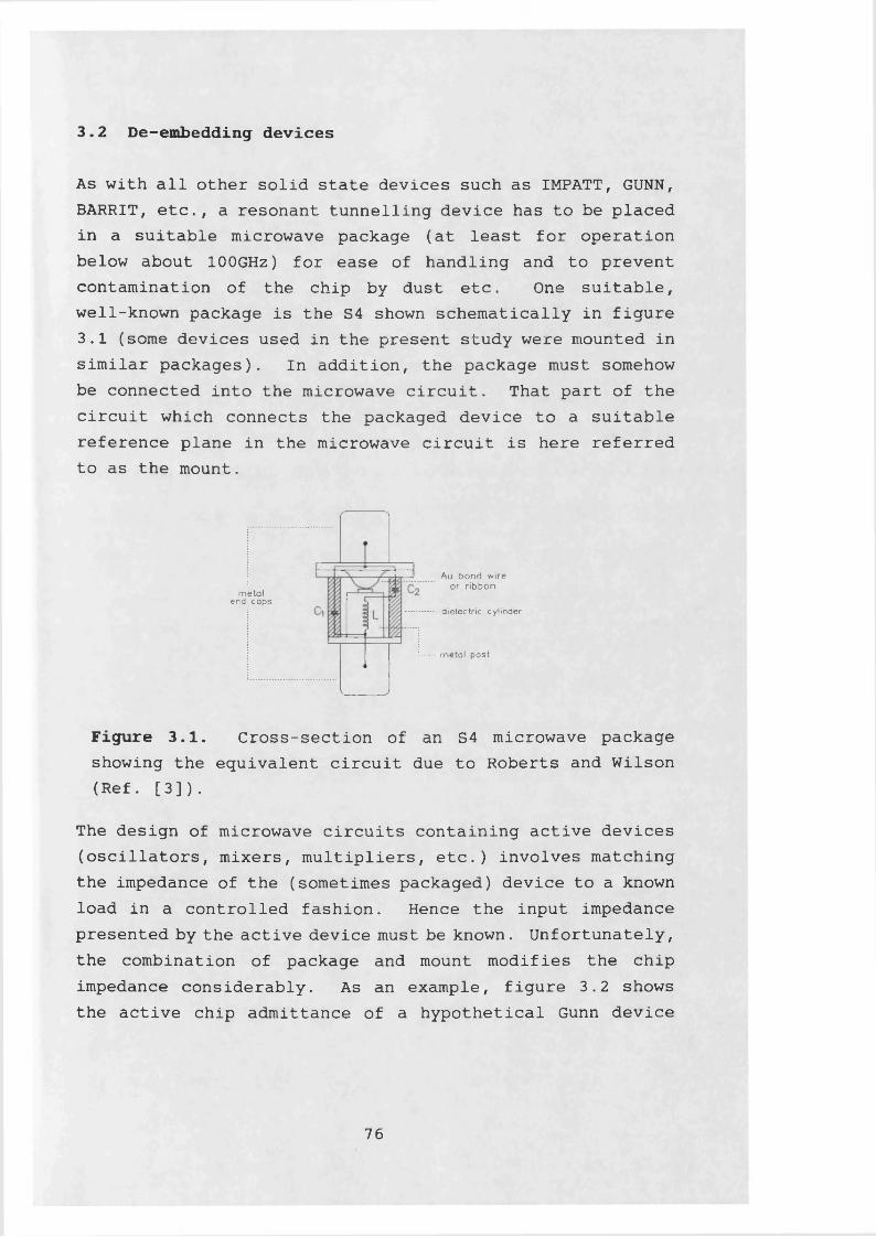
3.2 De-embedding devices
As with all other solid state devices such as IMPATT, GUNN, BARRIT, etc., a resonant tunnelling device has to be placed in a suitable microwave package (at least for operation below about 100GHz) for ease of handling and to prevent contamination of the chip by dust etc. One suitable, well-known package is the S4 shown schematically in figure3.1 (some devices used in the present study were mounted in similar packages). In addition, the package must somehow be connected into the microwave circuit. That part of the circuit which connects the packaged device to a suitable reference plane in the microwave circuit is here referred to as the mount.
metalend caps
Au bond wire or ribbon
dielectric cylinder
metal post
Figure 3.1. Cross-section of an S4 microwave package showing the equivalent circuit due to Roberts and Wilson (Ref. [3]).
The design of microwave circuits containing active devices (oscillators, mixers, multipliers, etc.) involves matching the impedance of the (sometimes packaged) device to a known load in a controlled fashion. Hence the input impedance presented by the active device must be known. Unfortunately, the combination of package and mount modifies the chip impedance considerably. As an example, figure 3.2 shows the active chip admittance of a hypothetical Gunn device
76
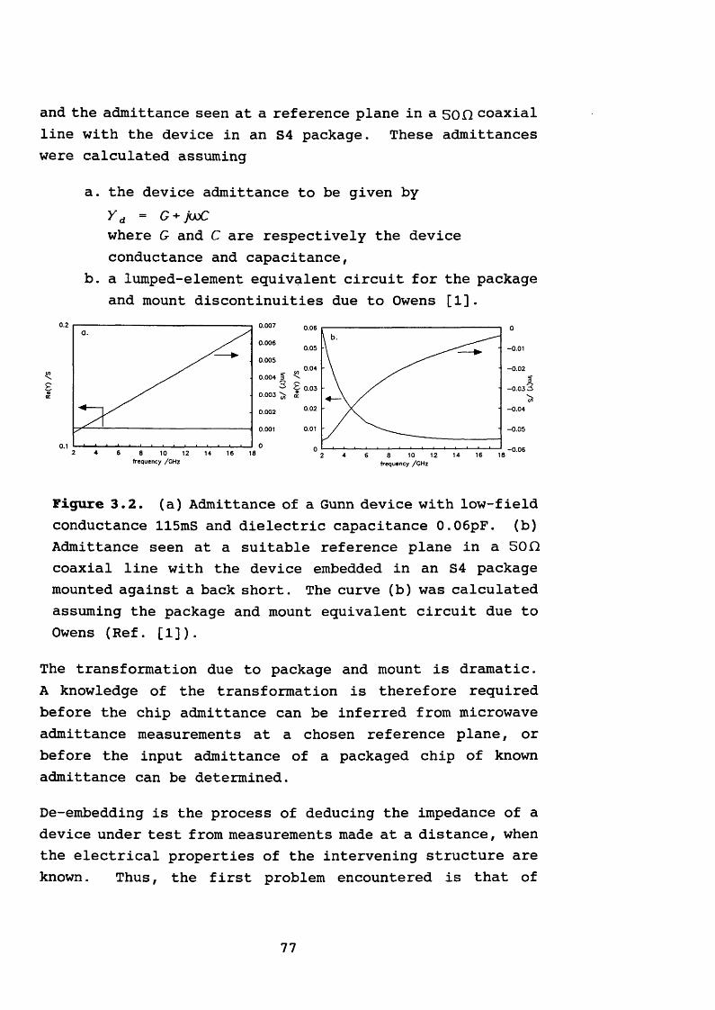
and the admittance seen at a reference plane in a 5 0 D coaxial line with the device in an S4 package. These admittances were calculated assuming
a. the device admittance to be given by Y d = G + juoCwhere G and C are respectively the device conductance and capacitance,
b. a lumped-element equivalent circuit for the package and mount discontinuities due to Owens [1].
0.2 0 .007 0 .0 6
0 .0 0 60 .0 5 - 0.01
0 .0 0 5
_ in 0 .0 0 4 zl_ \
0 .04 - 0.02in ■>■p 0 .0 3 - 0 .0 3 3eo:
0.02 - 0 .0 40.002
0.010.001 - 0 .0 5
0.1 - 0 .0 62 4 6 8 1810 12 1614frequency /GHz
Figure 3.2. (a) Admittance of a Gunn device with low-fieldconductance 115mS and dielectric capacitance 0.06pF. (b)Admittance seen at a suitable reference plane in a 50D coaxial line with the device embedded in an S4 package mounted against a back short. The curve (b) was calculated assuming the package and mount equivalent circuit due to Owens (Ref. [1]).
The transformation due to package and mount is dramatic. A knowledge of the transformation is therefore required before the chip admittance can be inferred from microwave admittance measurements at a chosen reference plane, or before the input admittance of a packaged chip of known admittance can be determined.
De-embedding is the process of deducing the impedance of a device under test from measurements made at a distance, when the electrical properties of the intervening structure are known. Thus, the first problem encountered is that of
77
characterising the package and mount discontinuity. There are two main schools of thought as to how this problem may be approached. The first involves the synthesis of lum- ped-element equivalent circuits for the mount and the package. The second represents the package and mount by a two-port network where one port is at the reference plane and the device (essentially a two-terminal one) is connected across the other. In the former case, the synthesis of a representative equivalent circuit of the mount and package is no easy matter, especially if the circuit is to be used at high frequencies and/or over a wide band of frequencies. However, valuable knowledge about the relative contributions of mount and package to the overall transformation is gained in the process. Two-port network representation, on the other hand is unique to a specific mount configuration and package and by its very nature will not convey any notion of the relative importance of mount and package on the reference plane impedance. Indeed, this method will be suitable only if de-embedding the active device is the primary objective. In any case the intervening structure between the reference plane and the actual device must be characterised prior to attempting measurement of the device at microwave frequencies. If we refer to this process as unterminating, then unterminating the package and mount discontinuities can be achieved either by lumped-element equivalent circuit modelling or by determining the ABCD matrix of a two-port equivalent network. These two methods will now be briefly reviewed.
3.2.1 Lumped-element equivalent circuit synthesis
The S4 and similar microwave packages have been the most popular and most widely studied of all (dc to ~20GHz) packages presently available. Gunn devices mounted in S4 packages are available and are well suited to half-wave coaxial-cavity
78
oscillators [2]. It had originally been assumed that thepackage may be represented by a lumped element low-passJi-network of the form indicated in figure 3.1.
The physical significance of the individual components of figure 3.1 may be explained by reference to Roberts and Wilson [3]. Ci is the capacitance between the lower portion of the post, through an air gap and the ceramic ring to the top cap, and C2 is the capacitance from the top of the post,through an air gap and the ceramic ring to the top cap.According to Roberts and Wilson [3], the inductance of the lead wire appeared to be negligible, but Owens and Cawsey[4] found it necessary to include this effect in their proposed package equivalent circuit. The parameters of this circuit were shown to be variant with change in measuring frequency, mount geometry and active device impedance [4].
Getsinger [5] retained the basic n circuit and derived additional components for mount geometry. This was achieved by subdividing the volume between chip and measurement plane into small regions each described by a lumped element circuit. Figure 3.3a illustrates the sub-regions chosen by Getsinger in deriving the equivalent circuit for the coaxial mount shown in figure 3.3c.
The subregions comprise
A - a coaxial line segment,B - a radial line segment, andC - a transition region with distorted electric and
magnetic fields (figure 3.3b).
A. Coaxial line segment
Assuming a lossless coaxial segment of small volume, the equivalent circuit of figure 3.4a may be used with L and C being the coaxial inductance and capacitance per unit length [6 ].
79
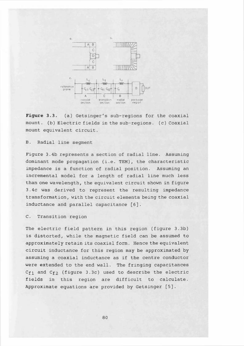
a. b.
referenceplane DUT
i i icoaxial transition radial packagesection section section region
Figure 3.3. (a) Getsinger's sub-regions for the coaxial mount, (b) Electric fields in the sub-regions, (c) Coaxial mount equivalent circuit.
B. Radial line segment
Figure 3.4b represents a section of radial line. Assuming dominant mode propagation (i.e. TEM), the characteristic impedance is a function of radial position. Assuming an incremental model for a length of radial line much less than one wavelength, the equivalent circuit shown in figure 3.4c was derived to represent the resulting impedance transformation, with the circuit elements being the coaxial inductance and parallel capacitance [6].
C. Transition region
The electric field pattern in this region (figure 3.3b) is distorted, while the magnetic field can be assumed to approximately retain its coaxial form. Hence the equivalent circuit inductance for this region may be approximated by assuming a coaxial inductance as if the centre conductor were extended to the end wall. The fringing capacitances Cfi and Cf2 (figure 3.3c) used to describe the electric fields in this region are difficult to calculate. Approximate equations are provided by Getsinger [5].
80
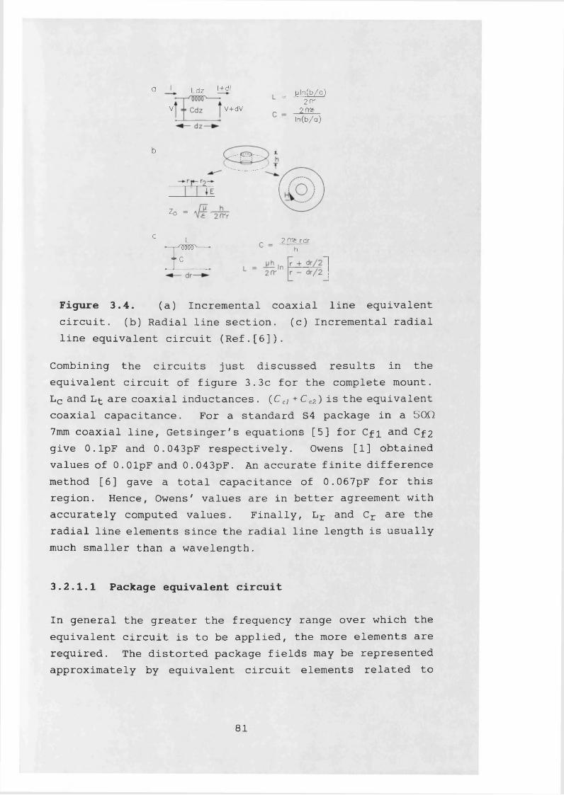
a Ldz |±d> ■ = P ln (b /a ) 2(TV V+dV 2 fra
ln (b /a )
b i
20 =
c L•—r W --•" C
2 fra rdr h
Figure 3.4. (a) Incremental coaxial line equivalentcircuit, (b) Radial line section, (c) Incremental radial line equivalent circuit (Ref.[6]).
Combining the circuits just discussed results in the equivalent circuit of figure 3.3c for the complete mount. Lc and Lt are coaxial inductances . (Ccl + C c2) is the equivalent coaxial capacitance. For a standard S4 package in a 500 7mm coaxial line, Getsinger's equations [5] for Cfi and Cf2 give 0.lpF and 0.043pF respectively. Owens [1] obtained values of O.OlpF and 0.043pF. An accurate finite difference method [6] gave a total capacitance of 0.067pF for this region. Hence, Owens' values are in better agreement with accurately computed values. Finally, Lr and Cr are the radial line elements since the radial line length is usually much smaller than a wavelength.
3.2.1.1 Package equivalent circuit
In general the greater the frequency range over which the equivalent circuit is to be applied, the more elements are required. The distorted package fields may be represented approximately by equivalent circuit elements related to
81
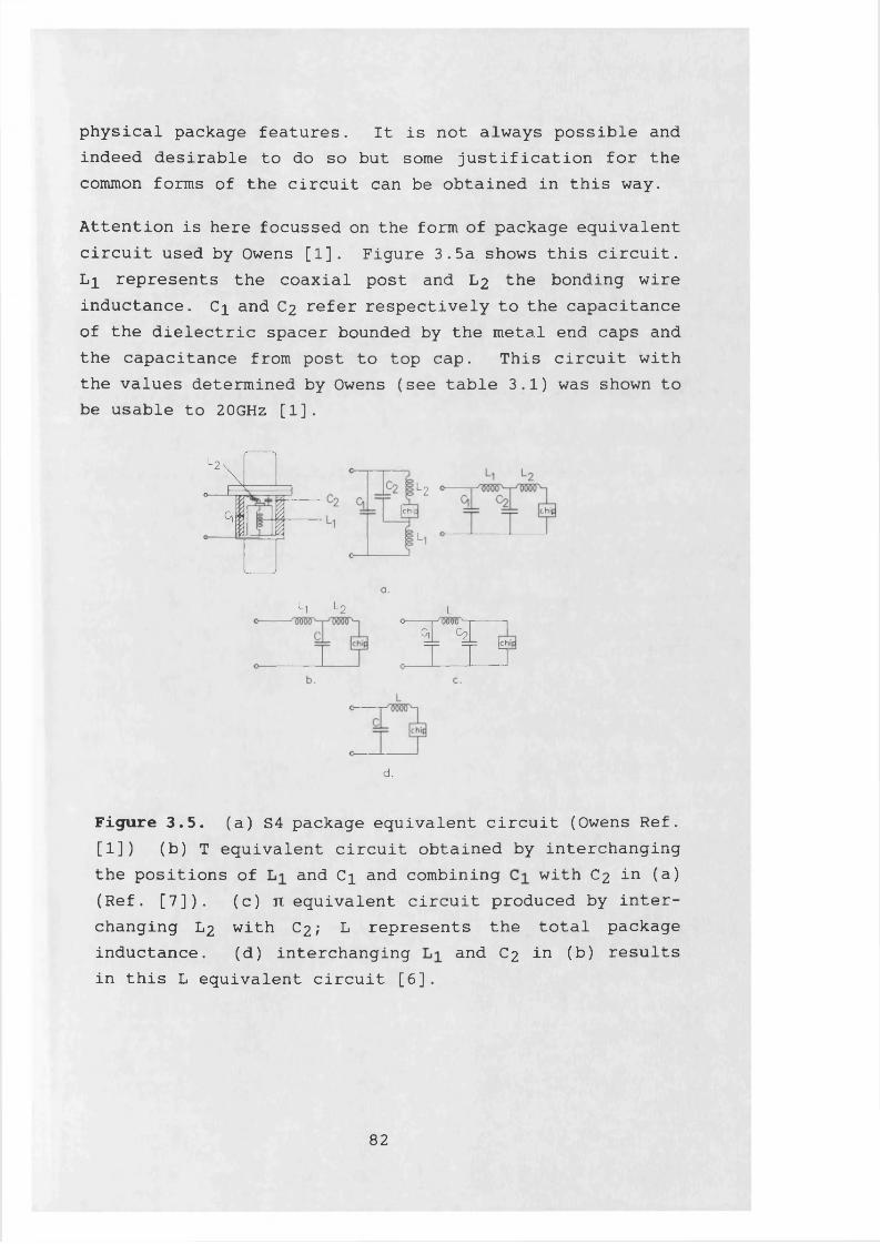
physical package features. It is not always possible and indeed desirable to do so but some justification for the common forms of the circuit can be obtained in this way.
Attention is here focussed on the form of package equivalent circuit used by Owens [1]. Figure 3.5a shows this circuit. Ll represents the coaxial post and L2 the bonding wire inductance. Ci and C2 refer respectively to the capacitance of the dielectric spacer bounded by the metal end caps and the capacitance from post to top cap. This circuit with the values determined by Owens (see table 3.1) was shown to be usable to 20GHz [1].
L>0---------^
Cl 1 iI
1
L2[c h i| C h i|
L
L1 l2
zLo--— r - wuu "-1-----1
1 it t g
d.
Figure 3.5. (a) S4 package equivalent circuit (Owens Ref.[1]) (b) T equivalent circuit obtained by interchangingthe positions of and C± and combining with C2 in (a) (Ref. [7]). (c) ji equivalent circuit produced by interchanging L2 with C2 ; L represents the total package inductance. (d) interchanging and C2 in (b) results in this L equivalent circuit [6].
82
This circuit can be simplified at lower frequencies. The impedance transformation due to a series L and shunt C combination remains approximately invariant when the order in which they appear in a circuit is reversed, provided that o)2ZC«l. Hence the positions of Li and Ci in figure 3.5a were interchanged and Ci combined with C2 to produce the circuit of figure 3.5b [7]. Similarly, if the positional order of L 2 and C2 is reversed in figure 3.5a, the circuit of figure 3.5c results in which L now represents the total package inductance.
Finally, by interchanging Li and C2 in figure 3.5b, the simple circuit of figure 3.5d is obtained [6 ]. This circuit is only accurate over a narrow frequency range but may be utilised to identify the principal resonances in the device-package interaction.
Various methods have been used to determine the package equivalent circuit elements, the most frequently cited work being due to Owens and Cawsey [4]. They assumed that the S4 package was lossless and used various internally short- and open-circuited dummy packages to derive a lumped-element equivalent circuit which eventually led to figure 3.6. The values of Lc, Lr , Cfi, Cf2 and represent the mount and were estimated by calculations based on Getsinger's work[5], while the remaining values, representing the package itself, were derived by a process of curve-fitting to the dummy package measurements.
83
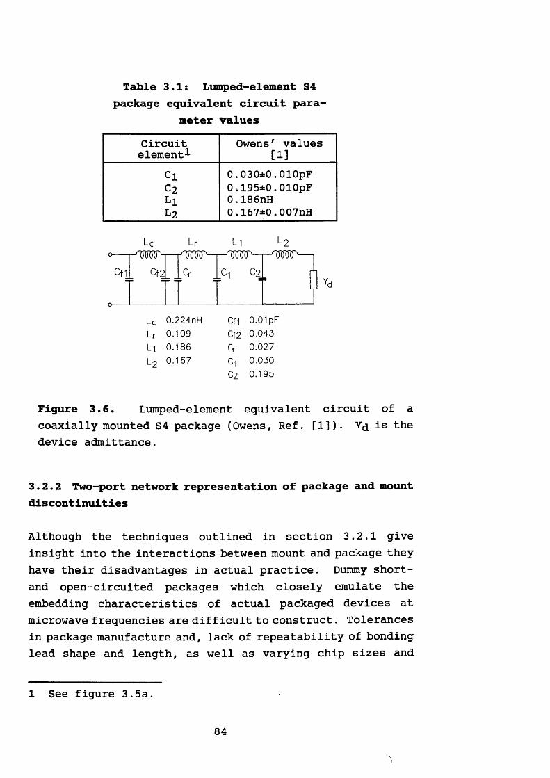
Table 3.1: Lumped-element S4package equivalent circuit para<
meter valuesCircuitelement^
Owens' values [1 ]
Cl 0.030±0.OlOpFC2 0.195±0.010pFLl 0.186nH^ 2 0.167±0.007nH
L1
Cflr-^000(P— r
Cf2 Cr q c2
l2
jYd
L c 0 .2 2 4 n H
L r 0 .1 0 9
L i 0 .1 8 6
L 2 0 .1 6 7
C fi 0.01 pF
Cf2 0 .0 4 3
Cr 0 .0 2 7
C-j 0 .0 3 0
C2 0 .1 9 5
Figure 3.6. Lumped-element equivalent circuit of a coaxially mounted S4 package (Owens, Ref. [1]). Y^ is the device admittance.
3.2.2 Two-port network representation of package and mount discontinuities
Although the techniques outlined in section 3.2.1 give insight into the interactions between mount and package they have their disadvantages in actual practice. Dummy short- and open-circuited packages which closely emulate the embedding characteristics of actual packaged devices at microwave frequencies are difficult to construct. Tolerances in package manufacture and, lack of repeatability of bonding lead shape and length, as well as varying chip sizes and
1 See figure 3.5a.
shapes give rise to a spread in package parasitics. Hence, precise equivalence in dummy- and device-package constructions is difficult to obtain. These factors introduce errors and uncertainties which give rise to the derivation of inaccurate device equivalent circuits. Moreover, the usefulness of an equivalent circuit such as the one of figure 3.6 is limited by the fact that the mount-dependent part is only usable in the configuration of figure 3.3a.
Another measurement technique, suitable for oscillators, makes use of a short-circuted dummy package and direct network analyser measurements to establish the reference plane at the chip terminals [8,9]. Pollard et al. [10] used a SOD tapered coaxial line as a probe to measure the admittance looking into the circuit from the position normally occupied by the device. This was achieved by connecting the 7mm end of the probe to a network analyser reflection test unit with the narrow end inserted into an axial hole drilled into a dummy package pedestal. The dummy package was replaced with a packaged Gunn device biased to the required operating point and power and frequency measurements made. The device admittance was then calculated using the basic equation for stable oscillations given by Kurokawa [11].
The latter technique, elegant as it may seem, is quite difficult to apply and has some inherent disadvantages. Although it is technologically possible to construct the probe it is by no means a simple problem to achieve a smooth taper from standard 7mm to less than 1mm coaxial air line; the least non-uniformity gives rise to significant inaccuracies, especially at high frequencies. Furthermore, the geometry of the package is altered by the pedestal hole and the presence of the probe, giving rise to fringing fields which perturb the package parasitics.
85
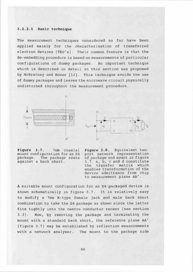
3.2.2.1 Basic technique
The measurement techniques considered so far have been applied mainly for the characterisation of transferred electron devices (TED7s ). Their common feature is that the de-embedding procedure is based on measurements of particular configurations of dummy packages. An important technique which is described in detail in this section was proposed by McBretney and Howes [12]. This technique avoids the use of dummy packages and leaves the microwave circuit physically undisturbed throughout the measurement procedure.
A
7 m m7nn//n//i/nmtllh
Figure 3.7. 7mm coaxial mount configuration for an S4 package. The package rests against a back short.
Figure 3.8. Equivalent two- port network representation of package and mount in figure 3.7. a, b, c and d constitute the transfer matrix which enables transformation of the device admittance from chip to measurement plane AA'.
A suitable mount configuration for an S4-packaged device is shown schematically in figure 3.7. It is relatively easy to modify a 7mm N-type female jack and male back short combination to take the S4 package as shown since the latter fits tightly into the centre conductor recess (see section 3.3). Now, by removing the package and terminating the mount with a standard back short, the reference plane AA' (figure 3.7) may be established by reflection measurements with a network analyser. The mount to the package side
86
along with the package itself may then be represented by the two-port network of figure 3.8, which is terminated by
the device admittance Y& [12,13]. ^ refer to the
transfer matrix of the two-port network such that the currents and voltages are related by [1 2 ]
(3.1)
Expanding (3.1) and dividing to obtain the admittance Ym looking into the plane AA' gives
Hence,
Y,
/j_ _ cV2 + dIz (3.1)V i aV 2 + b 12
c+dYd (3.2)a + bYn
Dividing the right hand side of (3.3) by d reduces this equation to
C + X „ (3.3)y,m A + B Y ,
where A, B and C are now the complex and frequency dependent transfer parameters characterising the two-port network. Ym can be measured directly with a network analyser. If this is done for three known values of Y^ in the frequency range of interest, then A, B and C can be solved simultaneously at each frequency. The problem is thus reduced to establishing known reference chip admittances. For the case of TED's, McBretney and Howes used the geometric magne- toresistance effect [14,15,16] whereby the application of a transverse magnetic field to a bulk semiconductor of suitable aspect ratio [17] (see note at the end of this
87
section) results in a decrease in its low field conductance G0 - McBretney and Howes have demonstrated that G0 remains constant at least up to about 20GHz. The measurement technique consisted basically in obtaining Ym in the frequency range of interest (2 - 18GHz) with the packaged and mounted device in a transverse magnetic field at three different flux densities between 0 and 2.5T. G0 was measured for each field setting using a resistance bridge.
If the Gunn device admittance can be modelled by a conductance G0 in parallel with a capacitance CQ , then from (3.3),
X m i {/l + £ ( G 01 + / u ) C 0 )} = C + G 0l + jw>C0 (3.4)
Y mZ{A + B(G02 + ju)C0)} = C + G 02 + y u ) C 0 (3.5)
y m3{y4 + 5(G03 + y(A)C0)> = C + G 03 + j<x>C0 (3.6)
where the numeric subscripts refer to the different magneticfield settings. Simultaneous solution of (3.4), (3.5) and (3.6) at each measurement frequency effectively characterises the two port network, providing that a reasonable estimate of CQ is available. In this respect, McBretney and Howes assumed CQ to be the dielectric capacitance and estimated it from the electrical parameters of the device by using,
sftoM'O
where pt0 and G 0 are the low field mobility and conductancerespectively (in the absence of a magnetic field), e is the permittivity and n0l the dopant concentration in the active layer.
If the device is removed from the magnetic field and biased to the required level, measurement of Ym will enable the transformation to be made to the chip itself, thus determiningYd-
88
The problem encountered in de-embedding a RTD in a microwave circuit by means of the two-port network representation is that of obtaining three known reference chip admittances. An identical approach to that used by McBretney and Howes cannot be used here because this approach pre-assumes the small-signal equivalent circuit model of the device. Furthermore, magnetotunnelling experiments with B parallel [18,19] and perpendicular [2 0 ,2 1 ,2 2 ] to J, carried out on double barrier RT heterostructures have demonstrated that there is little, if any, change in conductance, even at high magnetic fields, with the device biased below the resonant tunneling region. Indeed, these works have only shown a weakening and shifting to higher voltages of the features in the I-V characteristics. Moreover, since the capacitance varies appreciably with bias voltage, this situation is made even more difficult.
It may be possible and indeed fruitful, once an accurate device equivalent circuit has been established (at least at three distinct bias voltages), to apply a similar technique where the reference admittances are, instead, obtained by changing the device bias voltage. This would effectively eliminate the need for dummy packages and would lead to the determination of accurate small- and large-signal measurements.
Note: Aspect ratio for enhanced geometric magne tores is tance effectUnder strong magnetic fields, a significant increase in the resistivity of a bulk semiconductor is observed. For spherical energy surfaces the ratio of incremental resistivity to the bulk resistivity at zero magnetic field is approximately [15]
Ap ~ ,.2/?2 (a)— - \lnBP 0
where [in is the drift mobility for a semiconductor with n » p and B is the magnetic field component perpendicular to the direction of current flow.
89
Equation (a) should hold for a specimen of infinite extent. The effect of the shape of the specimen on Ap/p 0 is very significant [16]. It was shown by Willardson and Beer [17] that, for a square sample of side 1 and thickness d to give~ values approaching the theoretical, 1/d 1. Now, formost Gunn devices, the active layer thickness is between 2 and 8p.m and the surface dimensions between about 50x50 and 100x100p.m. Hence, the aspect ratio of most TED's is suitable for the observation of marked geometric magnetoresistance effects with fields of below ~ 2 T.
90
3.3 The S4-type package mount
The mounting arrangement shown schematically in figure 3.7 may in practice be obtained by a simple modification of a standard 7mm male N-type back short. Figure 3.9 shows the design. Use of 7mm N-type configurations facilitates design of coaxial mounts for S4 packages since the top and bottom caps fit tightly into the centre conductor recess on female jacks.
The centre pin of the standard back short was drilled out and substituted with the spring-loaded plunger arrangement shown. This plunger serves as a back short and pushes forward on the package so as to maintain good electrical contact.
The actual package used for mounting the first RTD's tested was the LEW Techniques^ type E3 with Cl/S covers, which is almost identical to the S4 package. Hence the lumped-element equivalent circuit of figure 3.6 was used with Owens' [1] parameter values, except for the value of L2 , the bond wire inductance, which was calculated from the known wire length and diameter.
1 LEW Techniques Ltd, 99 Taunton Trading Estates, Taunton, Somerset, England.
91
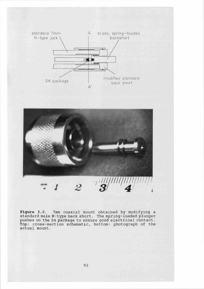
standard 7mm A brass, spring-loadedN— type jack backshort
modified standard back shortS4 package
A'
Figure 3.9. 7mm coaxial mount obtained by modifying a standard male N-type back short. The spring-loaded plunger pushes on the S4 package to ensure good electrical contact. Top: cross-section schematic, bottom: photograph of the actual mount.
92
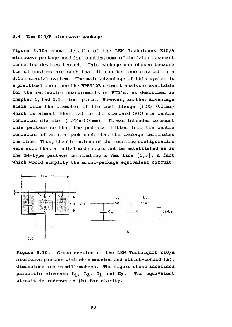
3.4 The El0/A microwave package
Figure 3.10a shows details of the LEW Techniques E10/A microwave package used for mounting some of the later resonant tunneling devices tested. This package was chosen because its dimensions are such that it can be incorporated in a 3.5mm coaxial system. The main advantage of this system is a practical one since the HP8510B network analyser available for the reflection measurements on RTD's, as described in chapter 4, had 3.5mm test ports. However, another advantage stems from the diameter of the post flange (1.30± 0.05mm) which is almost identical to the standard S OD sma centre conductor diameter (1.27± 0.03nm). It was intended to mount this package so that the pedestal fitted into the centre conductor of an sma jack such that the package terminates the line. Thus, the dimensions of the mounting configuration were such that a radial mode could not be established as in the S4-type package terminating a 7mm line [1,5], a fact which would simplify the mount-package equivalent circuit.
1.25 - 1.35
0.38 - 0.48
(b)
Device
Figure 3.10. Cross-section of the LEW Techniques E10/A microwave package with chip mounted and stitch-bonded (a), dimensions are in millimetres. The figure shows idealised parasitic elements L^, L2 , Ci and C2 . The equivalent circuit is redrawn in (b) for clarity.
93
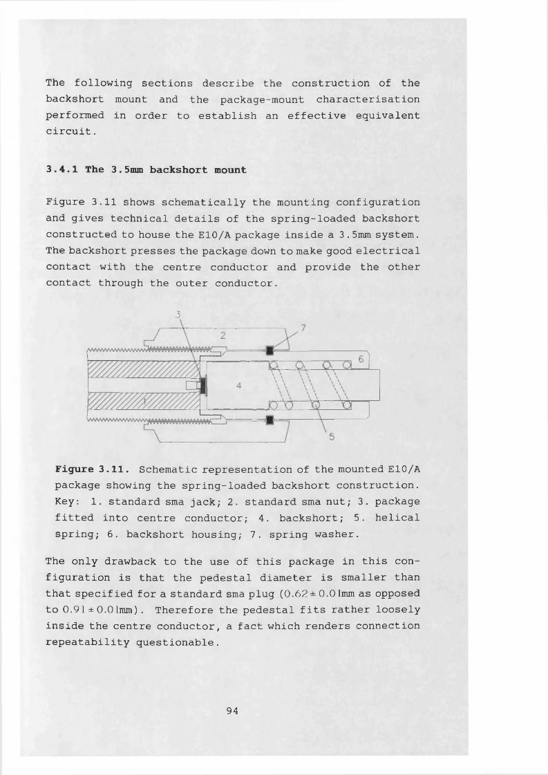
The following sections describe the construction of the backshort mount and the package-mount characterisation performed in order to establish an effective equivalent circuit.
3.4.1 The 3.5mm backshort mount
Figure 3.11 shows schematically the mounting configuration and gives technical details of the spring-loaded backshort constructed to house the E10/A package inside a 3.5mm system. The backshort presses the package down to make good electrical contact with the centre conductor and provide the other contact through the outer conductor.
3
Figure 3.11. Schematic representation of the mounted E10/A package showing the spring-loaded backshort construction. Key: 1. standard sma jack; 2. standard sma nut; 3. packagefitted into centre conductor; 4. backshort; 5. helical spring; 6. backshort housing; 7. spring washer.
The only drawback to the use of this package in this configuration is that the pedestal diameter is smaller than that specified for a standard sma plug (0.62 ± 0.0 lmm as opposed to 0.91 ± 0.01mm) . Therefore the pedestal fits rather loosely inside the centre conductor, a fact which renders connection repeatability questionable.
94
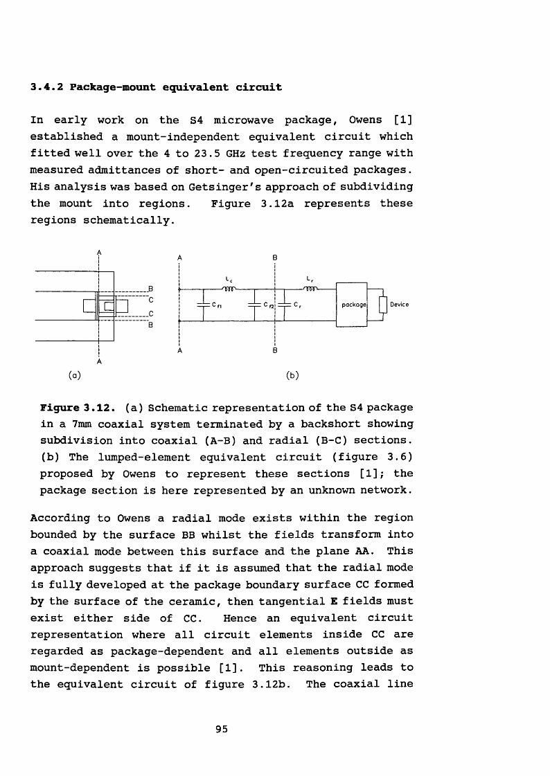
3.4.2 Package-mount equivalent circuit
In early work on the S4 microwave package, Owens [1] established a mount-independent equivalent circuit which fitted well over the 4 to 23.5 GHz test frequency range with measured admittances of short- and open-circuited packages. His analysis was based on Getsinger's approach of subdividing the mount into regions. Figure 3.12a represents these regions schematically.
□ package Device
(a) ( b )
Figure 3.12. (a) Schematic representation of the S4 packagein a 7mm coaxial system terminated by a backshort showing subdivision into coaxial (A-B) and radial (B-C) sections, (b) The lumped-element equivalent circuit (figure 3.6) proposed by Owens to represent these sections [1]; the package section is here represented by an unknown network.
According to Owens a radial mode exists within the region bounded by the surface BB whilst the fields transform into a coaxial mode between this surface and the plane AA. This approach suggests that if it is assumed that the radial mode is fully developed at the package boundary surface CC formed by the surface of the ceramic, then tangential E fields must exist either side of CC. Hence an equivalent circuit representation where all circuit elements inside CC are regarded as package-dependent and all elements outside as mount-dependent is possible [1]. This reasoning leads to the equivalent circuit of figure 3.12b. The coaxial line
95
section is represented by a coaxial inductance Lc flanked by fringing capacitances Cfi and Cf2 and the radial-line section by an inductance Lr and capacitance Cr .
Now, in the case of the E10/A package in the mount of figure 3.11, the diameter of the ceramic ring is approximately equal to that of the 500, 3.5mm coaxial line. Thus, although the E10/A and S4 packages and their respective mounts are similar (except for the dimensions), the assumption of a radial-line section for the E10/A mount is unjustifiable. Consequently it is not an easy matter to separate the equivalent circuit into a package-dependent part and a mount-dependent part, because there must be some interaction between the two along the ceramic ring surface.
The true field distribution within the package and in the area immediately surrounding must be extremely complex. However, one can still attempt to represent the package equivalent circuit as shown in figure 3.10b, where the package elements would have the following significance assuming no mount-package interaction:
Li: inductance of bond wireL2 : inductance of the protruding post and chipCi: capacitance between the chip surface, through an air
gap and the ceramic ring, and the top capC2 : capacitance between the pedestal flange, through an
air gap and the ceramic ring, and the top cap.Since it has been assumed that there is no radial-line section in the E10/A package mount, the package equivalent circuit elements must be effected by the mount. The ji-section including L2 flanked by Ci and C2 would now represent a coaxial-line section. 1*2 , Ci and C2 for the package regarded as a purely radial-line structure would be different. The true field situation lies somewhere between these two extremes and is effected significantly by the presence of a device chip of dimensions comparable to the package internal
96
dimensions. It is therefore not unreasonable to assume the radial-line structure as a starting point and treat the equivalent circuit elements as perturbed values, specifically that the series inductances and shunt capacitances are distributed differently. In this case there would be no need to consider mount and package separately and the resulting lumped element equivalent circuit representation would be simplified considerably.
3.4.3 Determination of the lumped equivalent circuit elements
The experimental procedure adopted for the determination of the package-mount equivalent circuit parameter values was similar in principle to that of Refs. [1], [2], and [4]. Reflection measurements were made over 0.5 to 13 GHz on four types of structure using an HP8510B network analyser calibrated at the package plane using a broadband and a sliding load as well as standard open and short circuits. The structures tested were the following:
1 . empty package
2 . dummy solid package
3. dummy open-circuited package
4. dummy short-circuited package
3.4.3.1 Measurements on the empty packages
For this structure the equivalent circuit of figure 3.10b would be reduced to just the capacitance C2 . Hence, the admittance looking into the package from the measurement plane should be the susceptance of C2 .
97
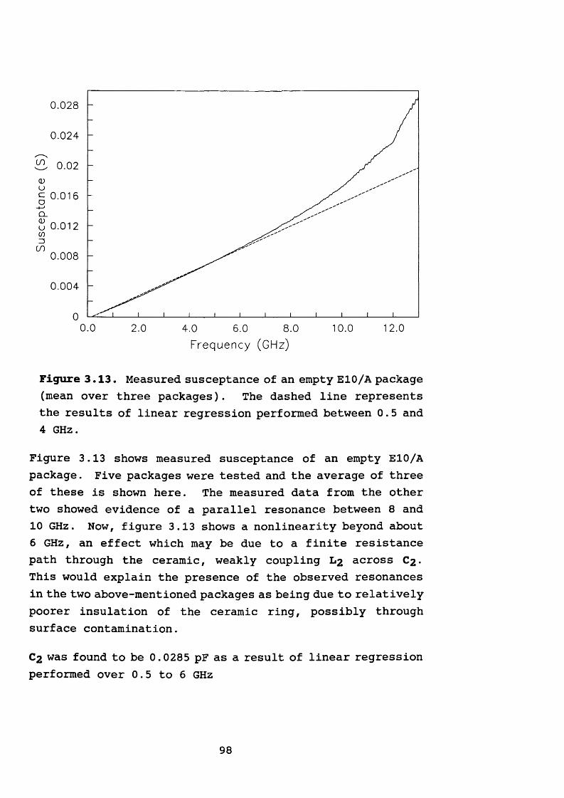
0.028
0.024
0.02
c 0.016
C l
0.012
000.008
0.004
0.0 2.0 12.010.04.0 6.0 8.0Frequency (GHz)
Figure 3.13. Measured susceptance of an empty E10/A package (mean over three packages). The dashed line represents the results of linear regression performed between 0 .5 and 4 GHz.
Figure 3.13 shows measured susceptance of an empty E10/A package. Five packages were tested and the average of three of these is shown here. The measured data from the other two showed evidence of a parallel resonance between 8 and 10 GHz. Now, figure 3.13 shows a nonlinearity beyond about 6 GHz, an effect which may be due to a finite resistance path through the ceramic, weakly coupling L2 across C2 - This would explain the presence of the observed resonances in the two above-mentioned packages as being due to relatively poorer insulation of the ceramic ring, possibly through surface contamination.
C2 was found to be 0.0285 pF as a result of linear regression performed over 0.5 to 6 GHz
98
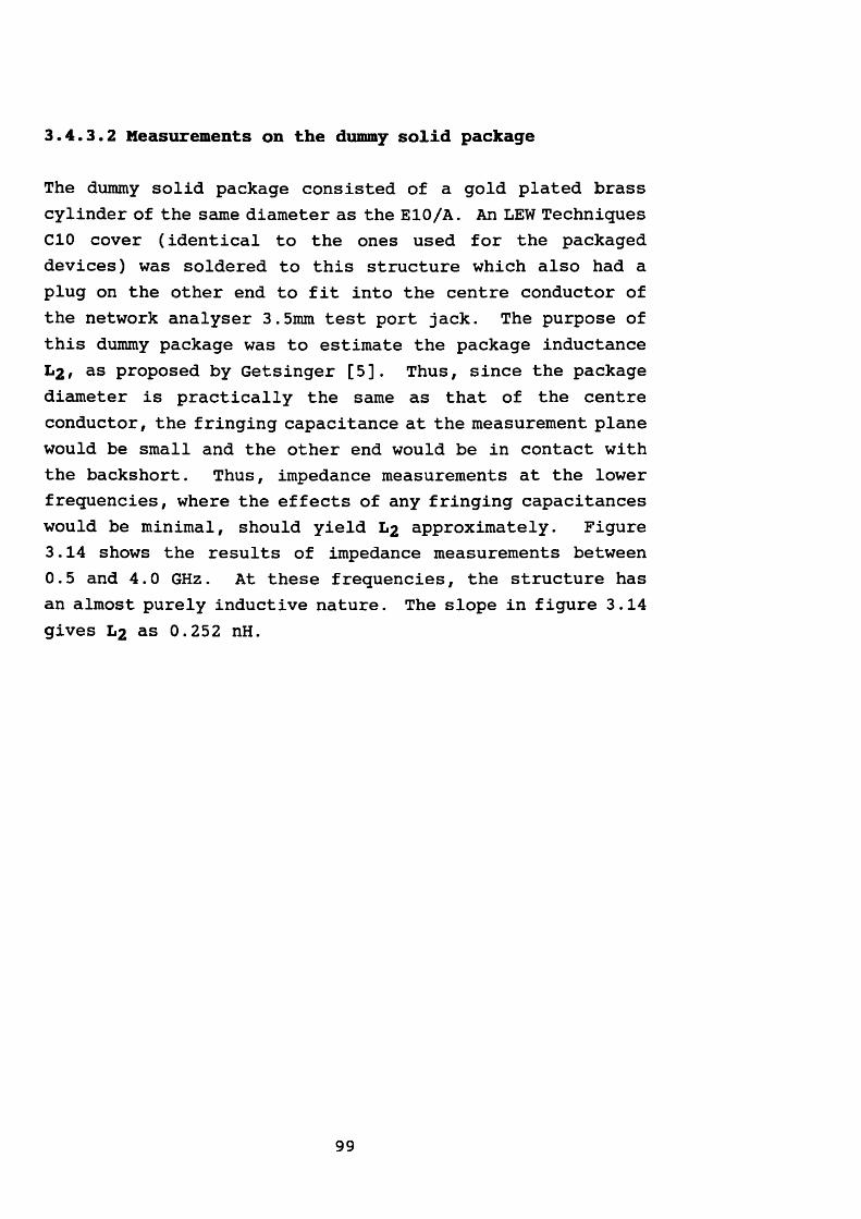
3.4.3.2 Measurements on the dummy solid package
The dummy solid package consisted of a gold plated brass cylinder of the same diameter as the E10/A. An LEW Techniques CIO cover (identical to the ones used for the packaged devices) was soldered to this structure which also had a plug on the other end to fit into the centre conductor of the network analyser 3.5mm test port jack. The purpose of this dummy package was to estimate the package inductance 1-2 f as proposed by Getsinger [5]. Thus, since the package diameter is practically the same as that of the centre conductor, the fringing capacitance at the measurement plane would be small and the other end would be in contact with the backshort. Thus, impedance measurements at the lower frequencies, where the effects of any fringing capacitances would be minimal, should yield l»2 approximately. Figure 3.14 shows the results of impedance measurements between 0.5 and 4.0 GHz. At these frequencies, the structure has an almost purely inductive nature. The slope in figure 3.14 gives L2 as 0.252 nH.
99
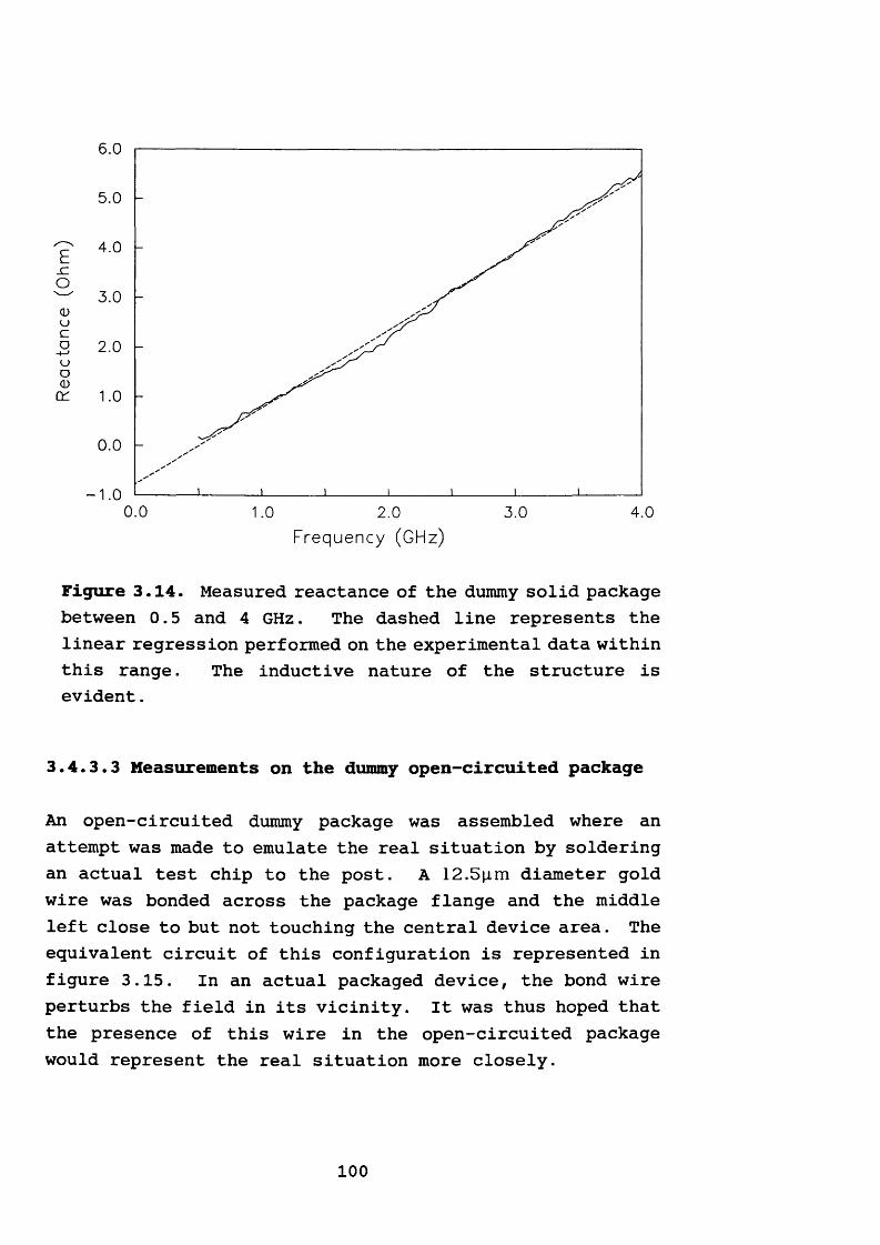
6.0
5.0
E 40_ CO
3.0CD u3 20u aCDC Z 1 .0
0.0
- 1.00.0 1.0 2.0 3.0 4.0
Frequency (GHz)
Figure 3.14. Measured reactance of the dummy solid package between 0.5 and 4 GHz. The dashed line represents the linear regression performed on the experimental data within this range. The inductive nature of the structure is evident.
3.4.3.3 Measurements on the dummy open-circuited package
An open-circuited dummy package was assembled where an attempt was made to emulate the real situation by soldering an actual test chip to the post. A 12.5n.rn diameter gold wire was bonded across the package flange and the middle left close to but not touching the central device area. The equivalent circuit of this configuration is represented in figure 3.15. In an actual packaged device, the bond wire perturbs the field in its vicinity. It was thus hoped that the presence of this wire in the open-circuited package would represent the real situation more closely.
J_____________ 1_____________ 1_____________ 1_____________ 1_____________ 1_____________ L
100
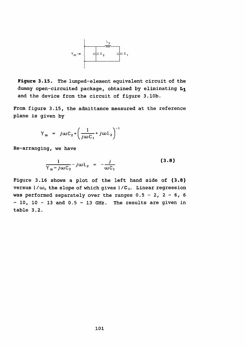
Figure 3.15. The lumped-element equivalent circuit of the dummy open-circuited package, obtained by eliminating and the device from the circuit of figure 3.10b.
From figure 3.15, the admittance measured at the reference plane is given by
Y m = /'ooCo + f . * + yuoLo )m J 2 VycxjC! z)
Re-arranging, we have
1 , j (3.8)---------- /coLo ------Y m - y CD C 2 (A) C !
Figure 3.16 shows a plot of the left hand side of (3.8) versus 1/co, the slope of which gives 1/Cj. Linear regression was performed separately over the ranges 0 . 5 - 2 , 2 - 6 , 6
- 10, 10 - 13 and 0.5 - 13 GHz. The results are given in table 3.2.
101
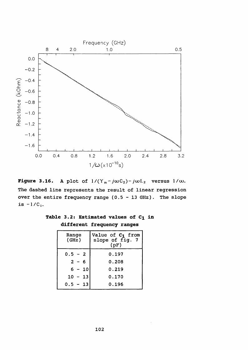
szO(D O Co
- t—'uoCDtr
2.0Frequency (GHz)
1.0 0.5
0.0- 0.2
- 0.8- 1.0
1.2
-1 .4
1.6
0.0 0.4 2.4 2.8 3.20.8 1.2 1.6 2.01/CJ(x10_10s)
Figure 3.16. A plot of l/(Ym -yooC2)-ycA)L2 versus 1/co.The dashed line represents the result of linear regression over the entire frequency range (0.5 - 13 GHz). The slope is - 1 /Cl
Table 3.2: Estimated values of Ci indifferent frequency ranges
Range(GHz)
Value of Ci from slope of fig. 7
(pF)0.5 - 2 0.197
2 - 6 0.2086 - 1 0 0.219
10 - 13 0.1700 . 5 - 1 3 0.196
102
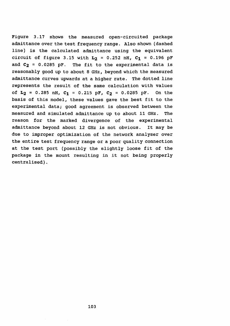
Figure 3.17 shows the measured open-circuited package admittance over the test frequency range. Also shown (dashed line) is the calculated admittance using the equivalent circuit of figure 3.15 with L2 = 0.252 nH, Ci = 0.196 pF and C2 = 0.0285 pF. The fit to the experimental data is reasonably good up to about 8 GHz, beyond which the measured admittance curves upwards at a higher rate. The dotted line represents the result of the same calculation with values of L2 = 0.285 nH, Ci = 0.215 pF, C2 = 0.0285 pF. On the basis of this model, these values gave the best fit to the experimental data; good agreement is observed between the measured and simulated admittance up to about 11 GHz. The reason for the marked divergence of the experimental admittance beyond about 12 GHz is not obvious. It may be due to improper optimization of the network analyser over the entire test frequency range or a poor quality connection at the test port (possibly the slightly loose fit of the package in the mount resulting in it not being properly centralised).
103
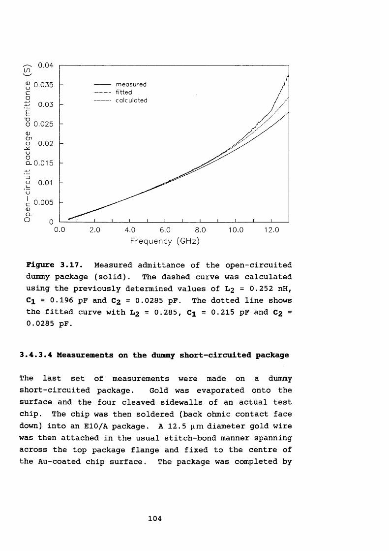
0.04
v 0.035 measuredfittedcalculated
0.03
a 0.025
Q- 0.01 5
0.005C l
0.0 12.02.0 6.0 10.04.0 8.0Frequency (GHz)
Figure 3.17. Measured admittance of the open-circuited dummy package (solid). The dashed curve was calculated using the previously determined values of L2 = 0.252 nH, Ci = 0 .196 pF and C2 = 0.0285 pF. The dotted line shows the fitted curve with L2 = 0.285, Ci = 0.215 pF and C2 = 0.0285 pF.
3.4.3.4 Measurements on the dummy short-circuited package
The last set of measurements were made on a dummy short-circuited package. Gold was evaporated onto the surface and the four cleaved sidewalls of an actual test chip. The chip was then soldered (back ohmic contact face down) into an E10/A package. A 12.5 pirn diameter gold wire was then attached in the usual stitch-bond manner spanning across the top package flange and fixed to the centre of the Au-coated chip surface. The package was completed by
104
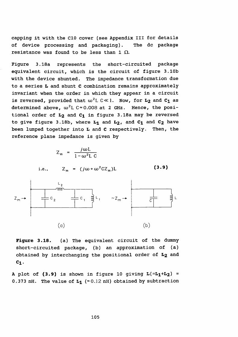
capping it with the CIO cover (see Appendix III for details of device processing and packaging). The dc package resistance was found to be less than 1 D.
Figure 3.18a represents the short-circuited package equivalent circuit, which is the circuit of figure 3.10b with the device shunted. The impedance transformation due to a series L and shunt C combination remains approximately invariant when the order in which they appear in a circuit is reversed, provided that oo2L C«l. Now, for and Cl as determined above, u>2L C * 0.008 at 2 GHz. Hence, the positional order of * 2 and Cl in figure 3.18a may be reversed to give figure 3.18b, where and L2 , and Cl and C2 have been lumped together into L and C respectively. Then, the reference plane impedance is given by
j ca)L 1 - ud2L C
i.e., Z m = (yco + co2CZm)L (3.9)
(a) (b)
Figure 3.18. (a) The equivalent circuit of the dummyshort-circuited package, (b) an approximation of (a) obtained by interchanging the positional order of 1*2 and Ci.
A plot of (3.9) is shown in figure 10 giving L(=Li+L2 ) = 0.373 nH. The value of (*0.12 nH) obtained by subtraction
105
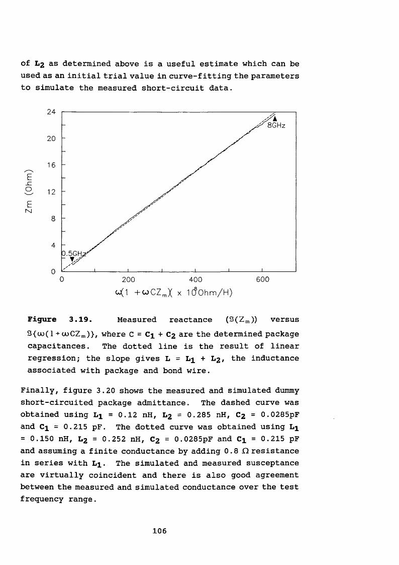
of I«2 as determined above is a useful estimate which can be used as an initial trial value in curve-fitting the parameters to simulate the measured short-circuit data.
24
8GHz
20
0.5GK
0 600200 400
cj(1 +coCZmX x 1C?0hm/H)
Figure 3.19. Measured reactance (3(Zm )) versusS{(A)(1 + coCZm)>, where C = Ci + C2 are the determined package capacitances. The dotted line is the result of linear regression; the slope gives L = Li + L2 , the inductance associated with package and bond wire.
Finally, figure 3.20 shows the measured and simulated dummy short-circuited package admittance. The dashed curve was obtained using Li = 0.12 nH, L2 = 0.285 nH, C2 = 0.0285pF and Ci = 0.215 pF. The dotted curve was obtained using Li = 0.150 nH, L2 = 0.252 nH, C2 = 0.0285pF and Ci = 0.215 pF and assuming a finite conductance by adding 0 . 8 D resistance in series with Li. The simulated and measured susceptance are virtually coincident and there is also good agreement between the measured and simulated conductance over the test frequency range.
106
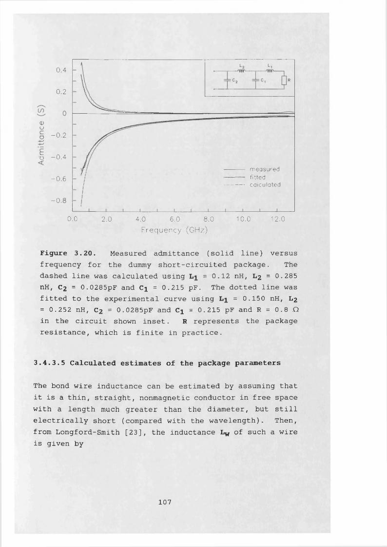
0.4
0.2
- 0.2
~o —0.4
measuredf i t t e dc a l c u la t e d
- 0.6
- 0.
0.0 2.0 8.0 10.0 12.04.0 6.0Frequency (GHz)
Figure 3.20. Measured admittance (solid line) versus frequency for the dummy short-circuited package. The dashed line was calculated using = 0.12 nH, L2 = 0.285 nH, C2 = 0.0285pF and Ci = 0.215 pF. The dotted line was fitted to the experimental curve using = 0.150 nH, L2 = 0.252 nH, C2 = 0.0285pF and Ci = 0.215 pF and R = 0.8 O in the circuit shown inset. R represents the package resistance, which is finite in practice.
3.4.3.5 Calculated estimates of the package parameters
The bond wire inductance can be estimated by assuming that it is a thin, straight, nonmagnetic conductor in free space with a length much greater than the diameter, but still electrically short (compared with the wavelength). Then, from Longford-Smith [23], the inductance Lw of such a wire is given by
107
where I and d are the length and diameter of the wire in inches, or,
with I and d in mm. I was estimated to be 0.40mm and d was12.5 (im, giving 1^ = 0.382 nH. Since a stitch-bond was used, would be half this value, assuming the bond to the chip occurs in the middle of the wire. This sets as 0.191 nH, which is of the same order of the fitted value of 0.150 nH.
Assuming L2 to be a purely coaxial inductance, independent of the ceramic, transmission line theory gives [24]
where d Q and d t are respectively the external and internalconductor diameters and h the package length («0.91 mm, complete with lid). An estimate of L2 as Lc in (3.11) gives L2 = 0 .232 nH which agrees well with the measured value of 0.252 nH.
Now, the field situation within the package is bound to be highly complex especially when considering that (a) the internal geometry of the package is significantly altered by the inclusion of a device chip which is large compared with the package dimensions and (b) the presence of the alumina ring (relative permittivity *9) very close to the post and chip (100-110pim separation). The assumption of Lc being a coaxial inductance is thus not strictly valid
nH (3.10)
(3.11)
and should be treated with caution. Any calculation of Ci and C2 would, for similar reasons, serve only as a very rough estimate.
An order-of-magnitude estimate of Ci and C2 may be made by assuming the region within the package ceramic ring outer surface to be a radial line section. Ci and C2 can then be approximated as parallel plate capacitances as suggested by Getsinger [5]. Such estimates give Ci = 0.34 pF and C2 =0.13 pF. Both, not surprisingly, differ significantly from the measured values.
3.4.4 Summary of results
In conclusion, a mount-dependent lumped element equivalent circuit of the LEW Techniques E10/A microwave package in a 50 fl 3.5mm mount terminated by a backshort has been proposed. Reflection measurements between 0.5 and 13 GHz were made with a network analyser on empty, dummy solid, open- and short-circuited packages leading to estimates of the parasitic elements. The model agrees well with experimental data for the short-circuited package, especially when allowance is made for an imperfect short circuit. The parameter values which gave the best fit are listed in table 3.3.
Table 3.3: Equivalent circuit parameter values for the El0/A package in the
mount of figure 3.11
Lx/nH L2/nH Ci/pF C2/pF0.150 0.252 0.215 0.0285
These values are subject to marginal changes from package to package due to manufacturing tolerances. Inconsistent bond wire length and shape is also bound to effect the value of L^. However, for chips of dimensions comparable to the
109
internal package dimensions, these changes would be negligible compared with changes in the parameter values brought about by varying chip sizes and shapes. The effect will be mostly on Ci and C2 since L2 has been shown to have a nearly coaxial nature. In this respect, the excellent agreement between the capacitances determined from the dummy open- and short-circuited packages is thought to be due to the choice of chips assembled in the respective packages. These were very carefully selected to have nearly identical dimensions and consequently the procedure was successful in pinning down fairly accurately the values of Ci and C2 -
110
References1. R. P. Owens, "Mount-independent equivalent circuit of the S4 diode package", Electron. Lett., Vol. 7, 1971, pp. 580-582.2. F. L. Warner and P. Herman, "Miniature X band Gunn oscillator with a dielectric tuning system", Electron. Lett., Vol. 12, 1966, pp. 467-468.3. D. A. E. Roberts and K. Wilson, "Evaluation of high quality varactor diodes", Proc. IEE Symp. Microwave Applications of Semiconductors (London), June 1965, pp. 22/1-22/8.4. R. P. Owens and D. Cawsey, "Microwave equivalent circuit parameters of Gunn-effect-device packages", IEEE Trans. Microwave Theory Tech., Vol. MTT-18, 1970, pp. 790-798.5. W. J. Getsinger, "The packaged and mounted diode as a microwave circuit", IEEE Trans. Microwave Theory Tech., Vol. MTT-14, 1966, pp. 58-69.6 . D. V. Morgan and M. J. Howes, "Microwave Solid StateDevices and Applications," Peter Peregrinus Ltd., 1980, pp. 72-86.7. P. T. Greiling and G. I. Haddad, "Large-signal equivalent circuits of avalanche transit-time devices", IEEE Trans. Microwave Theory Tech., Vol. MTT-18, 1970, pp. 842-852.8 . M. J. Howes and M. L. Jeremy, "Transferred-electronoscillator devices plane measurements", IEEE Trans. Electron Devices, Vol. ED-20, 1973, pp. 657-659.9. M. J. Howes and M. L. Jeremy, "Large signal circuitcharacterization of solid/state microwave oscillator devices", IEEE Trans. Electron Devices, Vol. ED-21, 1974, pp. 488-499.10. R. D. Pollard, M. J. Howes, and D. V. Morgan, "Design of BARRITT oscillators based on large-signal measurements," in Proc. 4th European Microwave Conf., Montreux, Switzerland, 1974, pp. 192-196.11. K. Kurokawa, "Some basic characteristics of broadband negative oscillator circuits", Bell Syst. Tech. J., Vol. 48, 1969, pp. 1937-1955.12. J. McBretney and M. J. Howes, "Electrical characterisation of transferred electron devices by a novel galva- nomagnetic technique", IEEE Trans. Microwave Theory Tech., Vol. MTT-27, 1979, pp. 256-265.13. R. F. Bauer and P. Penfield, Jr., "De-embedding and unterminating", IEEE Trans. Microwave Theory Tech., Vol. MTT-22, 1974, pp. 282-288.14. P. J. Bulman, G. S. Hobson, and B. C. Taylor, "Transferred Electron Devices," Academic Press, London, 1972.15. R. A. Smith, "Semiconductors," 2nd ed., Cambridge University Press, London, 1979.
Ill
16. E. H. Putley, "The Hall Effect and Related Phenomena," Butterworths, London, 1960.17. R. K. Wilardson, A. C. Beer, and A. E. Middleton, "Electrical properties of AlSb", J. Electrochem. Soc., Vol. 101, 1954, pp. 354-358.18. E. E. Mendez, L. Esaki, and W. I. Wang, "Resonant magnetotunneling in GaAlAs-GaAs-GaAlAs heterostructures", Phys. Rev. B, Vol. 33, 1986, 2893-2896.19. E. E. Mendez, "Physics of Resonant Tunneling in Semiconductors", in E. E. Mendez and K. von Klitzing (Ed.), "Physics and applications of Quantum Wells and Superlattices", Plenum Press, 1987.20. R. A. Davies, D. J. Newson, T. G. Powell, M. J. Kelly, and H. W. Myron, "Magnetotransport in semiconductor superlattices", Semicond. Science Tech., Vol. 2, 1987, pp. 61-64.21. M. L. Leadbeater, L. Eaves, P. E. Simmonds, G. A. Tombs, F. W. Sheard, P. A. Claxton, G. Hill, and M. A. Pate, "Magnetic field studies of negative differential conductivity in double barrier resonant tunnelling structures based on n~* InP/(InGa)As", Solid-State Electron., Vol. 31,1988, pp. 707-720.22. P. England, J. R. Hayes, M. Helm, J. P. Harbison, L. T. Florez, and S. J. Allen, Jr., "Resonant tunneling in crossed electric and magnetic fields", Appl. Phys. Lett., Vol. 54,1989, pp. 1469-1471.23. F. Longford-Smith, "Radio Designers Handbook," 4th ed., Iliffe, London, 1953.24. S. Ramo, J. R. Whinery, and T. Van Duzer, "Fields and Waves in Communication Electronics," John Wiley & Sons, New York, 1984.
112
CHAPTER 4
SMALL- AMD LARGE-SIGNAL DEVICE EQUIVALENT CIRCUITMODELS
4.1 Introduction
In this chapter, the measurement of small-signal and large-signal device admittance will be discussed with particular reference to the actual techniques used in this work. Thus, it is worthwhile to discuss briefly what is meant by the two terms.
4.1.1 Small- and large-signal admittance
The admittance (or impedance) of an active microwave solid state device is generally a function of frequency for high rf currents (7r/). However, at very small rf drive levels, the admittance becomes virtually independent of /r/ such that the rf current and voltage are linearly related by
lr, “ Y t V r, ( 4 - 1 )
In this region, the device is said to operate in its small-signal regime. Oscillators and amplifiers incorporating solid state devices operating under large-signal conditions are perhaps not best described by their small-signal admittance (or impedance) as this is obviously not a faithful description under these conditions. However, small-signal characterisation is useful:
a. for linear amplifier design.
113

b. for preliminary design of nonlinear circuits such as oscillators,
c. because the admittance is independent of Irf and hence of incident microwave power,
d. the admittance requires low microwave power for its measurement which enables the use of standard network analysers,
e. the small-signal admittance of most solid-state devices can often be quite easily modelled and computed, from known physical and electrical parameters, thus facilitating comparisons of theoretical predictions and small-signal measurements which may lead to greater understanding of the device,
f. small-signal equivalent circuits determined over a sufficiently wide bias voltage range may be used in large-signal combined time-frequency domain analysis (see chapter 5).
When Irf is large enough such that any nonlinear region (orregions) of the device characteristic I-V relationship is (are) swept to any significant degree during the rf cycle, the device admittance may become a rapidly varying function of both frequency and signal amplitude. This is often the case with oscillators and frequency multipliers.
4.2 Small-signal measurements
Having distinguished between small- and large-signal device behaviour this section discusses small-signal equivalent circuits of resonant tunnelling devices. Experiments and
114
analysis leading to the successful determination of the small-signal equivalent circuit model elements between 45 MHz and 13 GHz over a wide range of bias voltages are described. The effect of test signal power upon the measurements is also discussed and shown to be an important consideration.
4.2.1 Small-signal equivalent circuit model of the RTD 523B
The subject of this study was the double barrier resonant tunnelling heterostructure No. 523. This is an MOCVD structure grown by Siemens, the details of which are given in chapter 2. The wafer sections available were 400 pim thick and had a back ohmic contact. They were thus not suitable for mounting into E10/A packages as the gap between the post and top cap is less than 500 p.m.
Wafer sections of the 523 heterostructure were lapped down mechanically from the substrate side to about 2 0 0 pim thickness. A fresh Au-Ge ohmic contact layer was then evaporated to form the new back contact. The wafers were subsequently subjected to rapid thermal annealing and individual devices scribed and diced into ~300x300nm2 chips. Devices with top contact areas of S O x S O u m 2 and 20x20^im2 were mounted into E10/A packages and bonded with 12.5 p,m-diameter gold wire3*. Re-processing of these wafers in most cases did not alter their dc characteristics significantly. The measurements described in this section were performed on a 2 0 x 2 0 n m 2 device, henceforth to be referred to as the 523B.
1 Details of the device processing are given in AppendixIII.
115
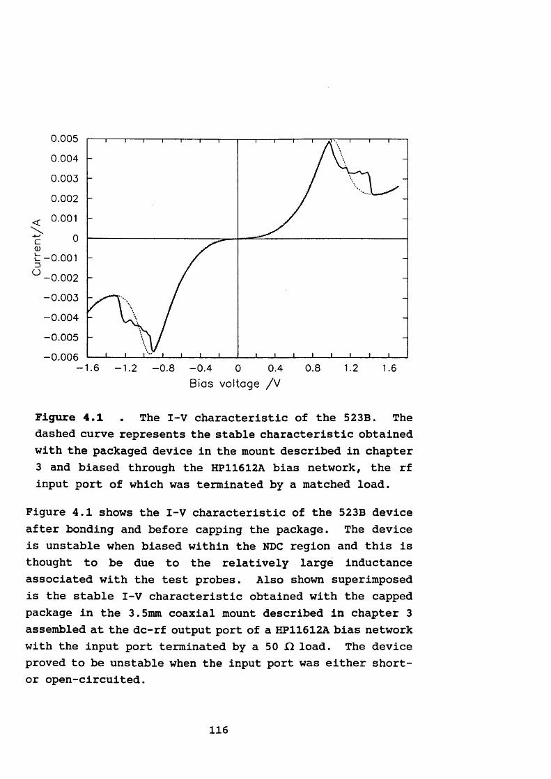
0.005
0.0040.0030.0020.001
c 0<Dh -0.001
- 0.002-0.003-0.004-0.005-0.006
1.6 -1.2 -0.8 -0.4 0.8 1.2 1.60 0.4Bias vo ltage / V
Figure 4.1 . The I-V characteristic of the 523B. Thedashed curve represents the stable characteristic obtained with the packaged device in the mount described in chapter 3 and biased through the HP11612A bias network, the rf input port of which was terminated by a matched load.
Figure 4.1 shows the I-V characteristic of the 523B device after bonding and before capping the package. The device is unstable when biased within the NDC region and this is thought to be due to the relatively large inductance associated with the test probes. Also shown superimposed is the stable I-V characteristic obtained with the capped package in the 3.5mm coaxial mount described in chapter 3 assembled at the dc-rf output port of a HP11612A bias network with the input port terminated by a 50 D load. The device proved to be unstable when the input port was either short- or open-circuited.
116
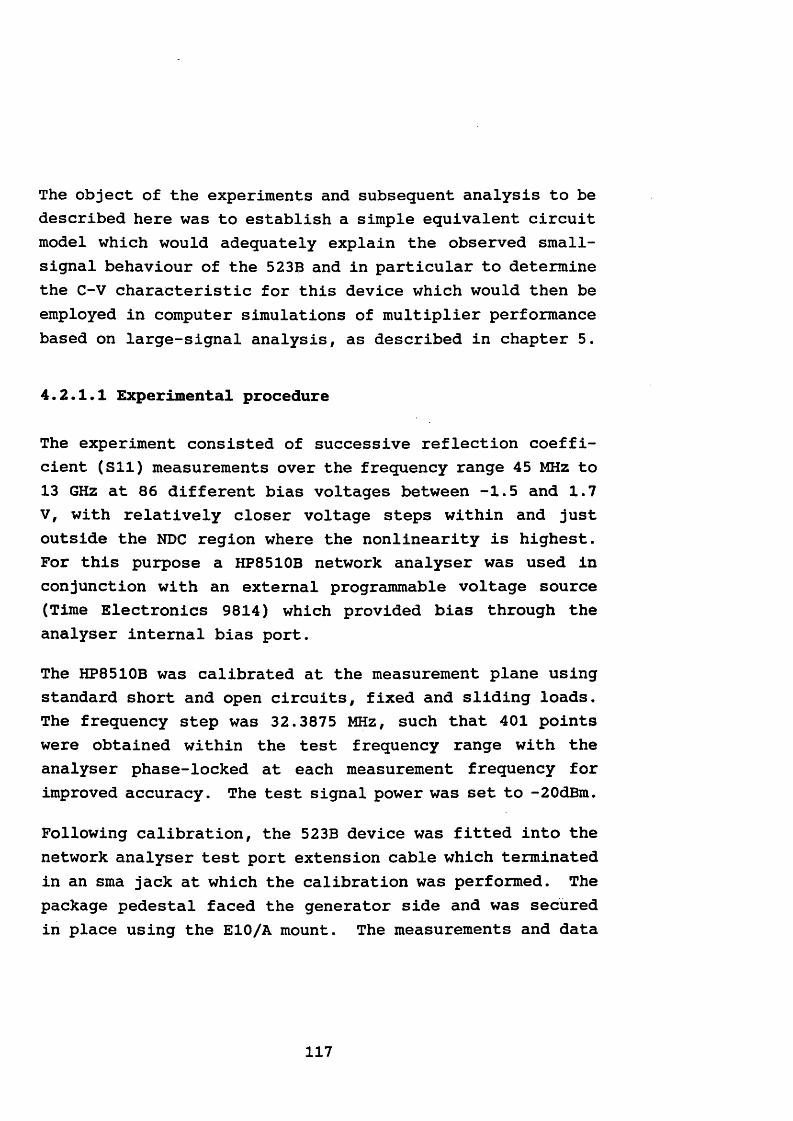
The object of the experiments and subsequent analysis to be described here was to establish a simple equivalent circuit model which would adequately explain the observed small- signal behaviour of the 523B and in particular to determine the C-V characteristic for this device which would then be employed in computer simulations of multiplier performance based on large-signal analysis, as described in chapter 5.
4.2.1.1 Experimental procedure
The experiment consisted of successive reflection coefficient (Sll) measurements over the frequency range 45 MHz to 13 GHz at 8 6 different bias voltages between -1.5 and 1.7 V, with relatively closer voltage steps within and just outside the NDC region where the nonlinearity is highest. For this purpose a HP8510B network analyser was used in conjunction with an external programmable voltage source (Time Electronics 9814) which provided bias through the analyser internal bias port.
The HP8510B was calibrated at the measurement plane using standard short and open circuits, fixed and sliding loads. The frequency step was 32.3875 MHz, such that 401 points were obtained within the test frequency range with the analyser phase-locked at each measurement frequency for improved accuracy. The test signal power was set to -20dBm.
Following calibration, the 523B device was fitted into the network analyser test port extension cable which terminated in an sma jack at which the calibration was performed. The package pedestal faced the generator side and was secured in place using the E10/A mount. The measurements and data
117
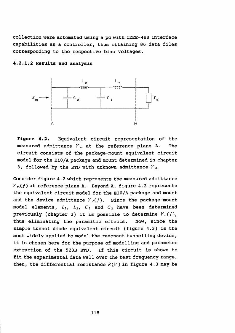
collection were automated using a pc with IEEE-488 interface capabilities as a controller, thus obtaining 8 6 data files corresponding to the respective bias voltages.
4.2.1.2 Results and analysis
Figure 4.2. Equivalent circuit representation of the measured admittance Y m at the reference plane A. The circuit consists of the package-mount equivalent circuit model for the E10/A package and mount determined in chapter 3, followed by the RTD with unknown admittance Y d.
Consider figure 4.2 which represents the measured admittance ^m(/) at reference plane A. Beyond A, figure 4.2 represents the equivalent circuit model for the E10/A package and mount and the device admittance Y d(f). Since the package-mount model elements, Llt Lz, C x and C2 have been determined previously (chapter 3) it is possible to determine ^ d(/)/ thus eliminating the parasitic effects. Now, since the simple tunnel diode equivalent circuit (figure 4.3) is the most widely applied to model the resonant tunnelling device, it is chosen here for the purpose of modelling and parameter extraction of the 523B RTD. If this circuit is shown to fit the experimental data well over the test frequency range, then, the differential resistance R(V) in figure 4.3 may be
118
i
obtained from the dc I-V characteristic leaving R s, the series resistance and C(K) to be determined from the reflection measurements. R s should be nominally independent of frequency while C in this model is assumed to depend only on bias voltage.
The first step in the analysis is to obtain an estimate of the series resistance R s. Referring to figure 4.3, the device impedance, Z d, has real and imaginary parts given by
_ / *7 "v n R <4 -2)K(Zd) - Rs +--------- -1 + ( cjoC/?)
uoCR2 (4.3)a ( Z -> ’
c(v)=i= G(V)=1/R(V)
Figure 4.3 . Equivalent circuit model assumed for theRTD 523B. R s is the series resistance, G(K)the differential conductance and C(K) the capacitance. Y d is the device admittance.
Thus, C may be calculated from (4.3) by assuming the value of R obtained from the I-V characteristic at any bias voltage and frequency within the test ranges. R s can then be estimated by substituting for R and C in (4.2). This procedure was performed using the de-embedded measured impedance at the
119
minimum positive differential resistance bias points (prior to the current peaks in forward and reverse bias). A mean value of 4.4±0.5Hwas obtained over the test frequency range.
A more convenient, and possibly more accurate, method of determining the capacitance is as follows. Having estimated the series resistance, and assuming this is approximately independent of frequency and bias voltage, the effect of R a on Y d is subtracted out, giving the intrinsic admittance Y intr as
Z intr ~ Z d~ R s
Lq-> yintr(“>)= G(V) + ju>C(V) 4)
where G = 1/R is the differential conductance. Thus, the slope of the susceptance versus frequency plot gives C(K). The mean value of <X (co)> over the frequency range gives another estimate of G(K).
In practice, this procedure was coded in FORTRAN and the slope determined at each bias point over the test frequency range by using a linear regression algorithm. The percentage standard error of the slope was between less than 1 % and up to about 3%. In each case the intercept was negligibly small and comparable in magnitude to its respective standard error. The results of these calculations are given in figure4.4 which is a plot of the capacitance as a function of bias voltage. Since the small-signal analysis was based on measurements of Sll, this is essentially a differential capacitance. The asymmetry in the C-V characteristic is probably due to unintentional asymmetry in the structure of the 523B. This is also evident from the I-V and G-V characteristics of figure 4.1 and 4.5, respectively.
120
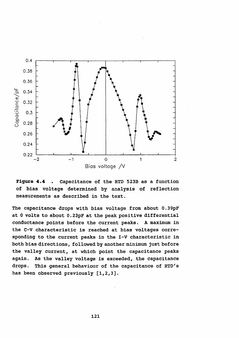
0.4
0.380.36
l_L_Q- 0.340.320.3
Q.
0.260.240.22-2 20 1
Bias vo lta ge / V
Figure 4.4 . Capacitance of the RTD 523B as a functionof bias voltage determined by analysis of reflection measurements as described in the text.
The capacitance drops with bias voltage from about 0.39pF at 0 volts to about 0.23pF at the peak positive differential conductance points before the current peaks. A maximum in the C-V characteristic is reached at bias voltages corresponding to the current peaks in the I-V characteristic in both bias directions, followed by another minimum just before the valley current, at which point the capacitance peaks again. As the valley voltage is exceeded, the capacitance drops. This general behaviour of the capacitance of RTD's has been observed previously [1,2,3].
121
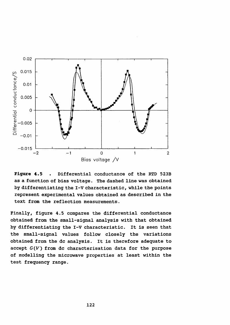
0.02
0.015
0.01
X) 0.005
0
£-0. 0 0 5
o- 0.01
-0.015-2 2- 1 0 1
Bias vo ltage / V
Figure 4.5 . Differential conductance of the RTD 523Bas a function of bias voltage. The dashed line was obtained by differentiating the I-V characteristic, while the points represent experimental values obtained as described in the text from the reflection measurements.
Finally, figure 4.5 compares the differential conductance obtained from the small-signal analysis with that obtained by differentiating the I-V characteristic. It is seen that the small-signal values follow closely the variations obtained from the dc analysis. It is therefore adequate to accept G(K) from dc characterisation data for the purpose of modelling the microwave properties at least within the test frequency range.
122
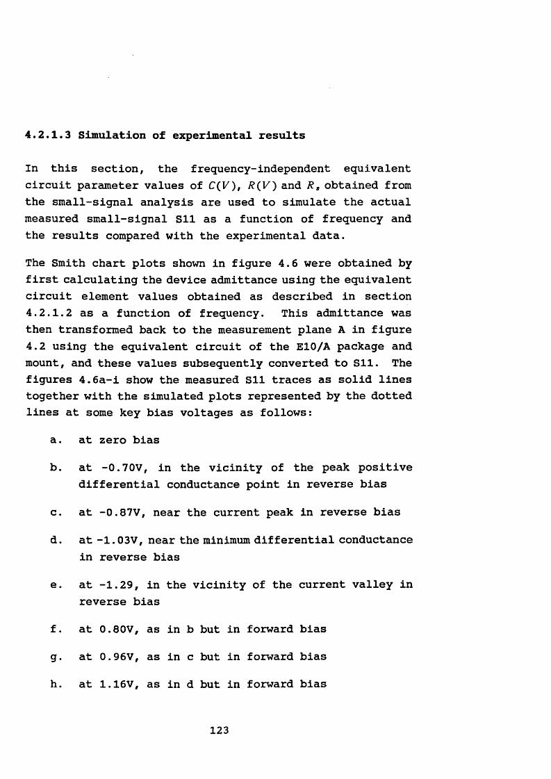
4.2.1.3 Simulation of experimental results
In this section, the frequency-independent equivalent circuit parameter values of C(K), /?(K) and R s obtained from the small-signal analysis are used to simulate the actual measured small-signal Sll as a function of frequency and the results compared with the experimental data.
The Smith chart plots shown in figure 4.6 were obtained by first calculating the device admittance using the equivalent circuit element values obtained as described in section4.2.1.2 as a function of frequency. This admittance was then transformed back to the measurement plane A in figure4.2 using the equivalent circuit of the E10/A package and mount, and these values subsequently converted to Sll. The figures 4.6a-i show the measured Sll traces as solid lines together with the simulated plots represented by the dotted lines at some key bias voltages as follows:
a. at zero bias
b. at -0.70V, in the vicinity of the peak positive differential conductance point in reverse bias
c. at -0.87V, near the current peak in reverse bias
d. at -1.03V, near the minimum differential conductance in reverse bias
e. at -1.29, in the vicinity of the current valley inreverse bias
f. at 0.80V, as in b but in forward bias
g. at 0.96V, as in c but in forward bias
h. at 1.16V, as in d but in forward bias
123
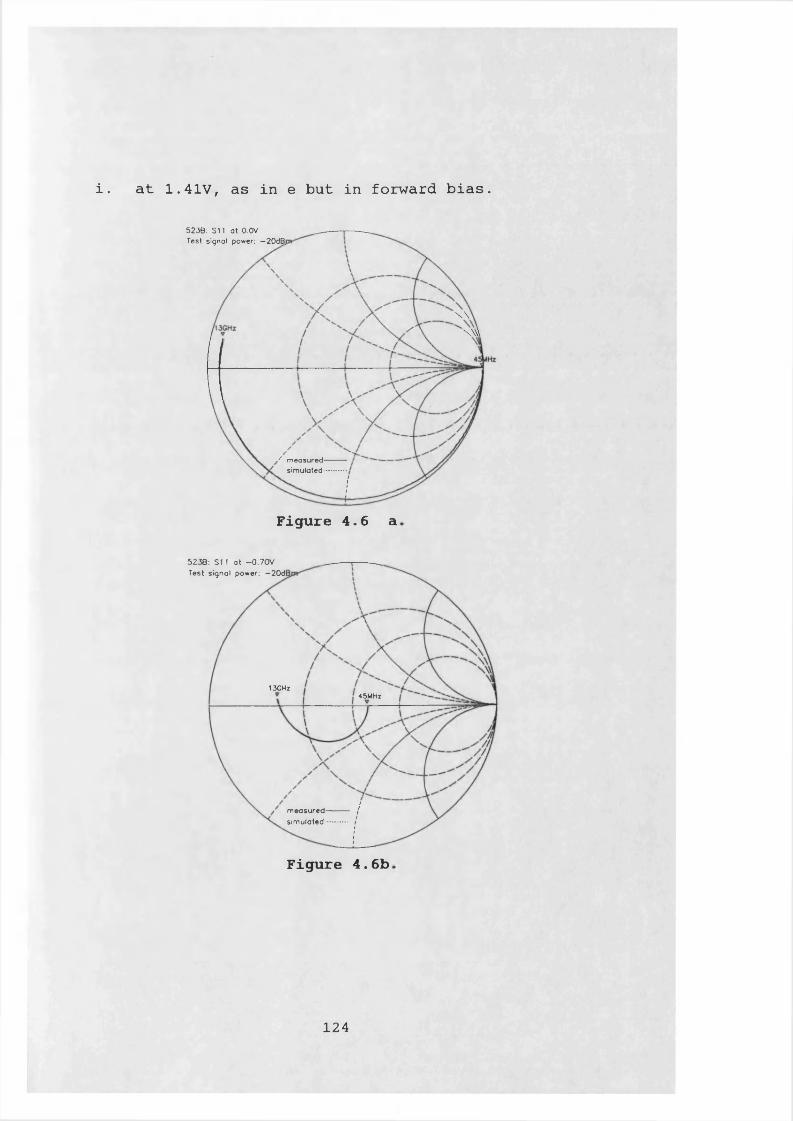
i. at 1.41V, as in e but in forward bias.
5238: S11 ot 0.0V Test signal power: —20dBj
w\w\
/ measured- simulated
Figure 4.6 a
5238: St 1 ot -0.70V Test signal power: — 20dl
13GHz45MHz
measured-simulated
Figure 4.6 b
124
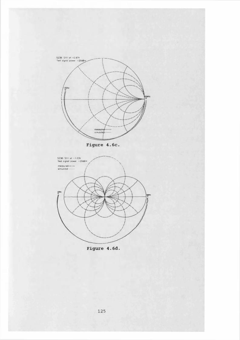
5236: S11 ot -0 .87 VTest signal power: -20dBm ,
\ V
■\W\
simulated
Figure 4.6c
5238: S l l ot - 1.03V V NTest signol power: -20dBm / \
measured / \simulated / \
Figure 4.6d.
125
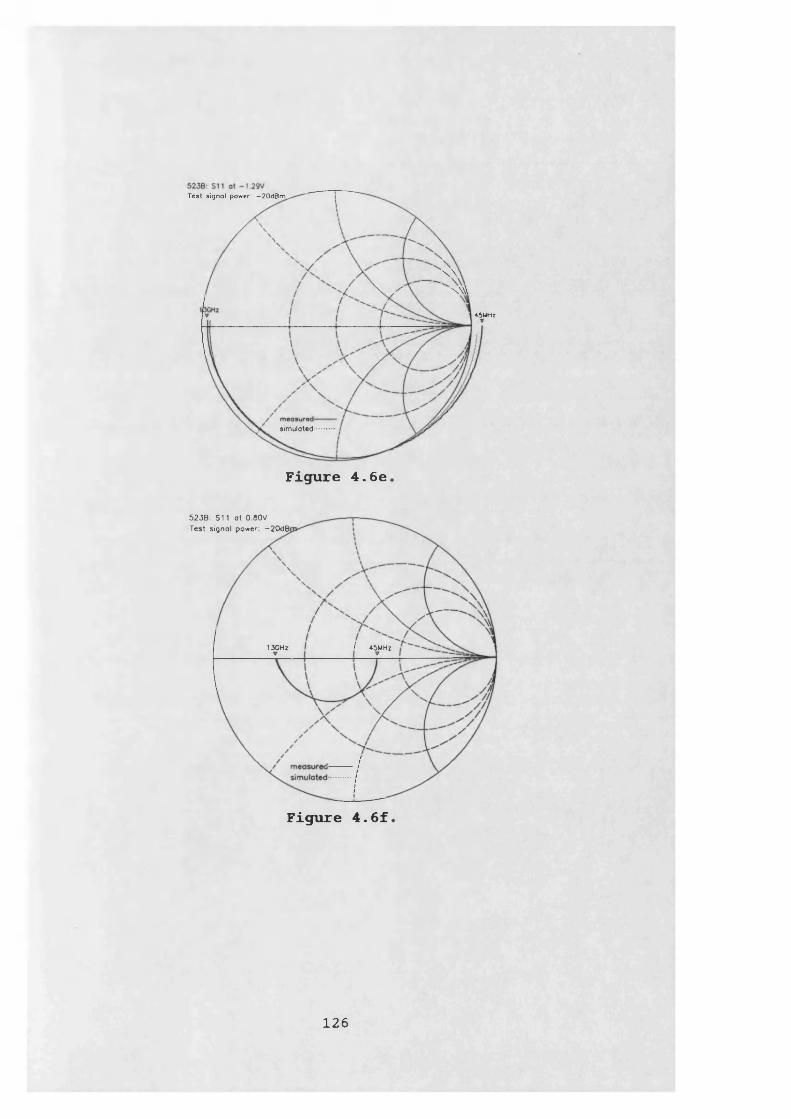
T e s t s ig n a l pow er: - 2 0 d 9 m
wxw\
45MHz
simulated-
Figure 4.6e
523B: S11 ot 0.80V Test signal power: -20dBi
/ 45M Hz13GHz
Figure 4.6f
126
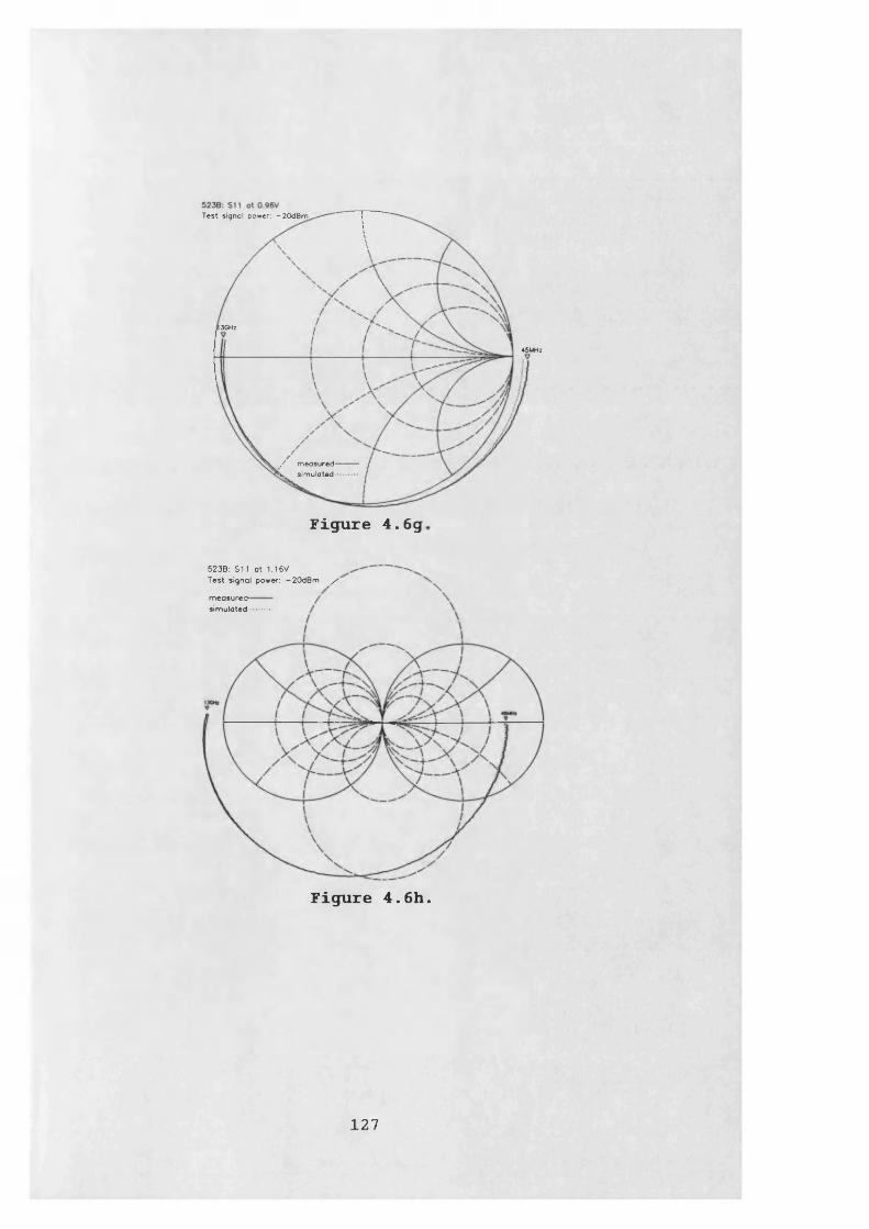
T e st s igna l power: -2 0 d B m
3GHz
45MHz
/ measured---------k simulated —
Figure 4.6g
523B: S11 ot 1.16VTest signal power: -20d8m /
measured'simulated-
Figure 4.6h.
127
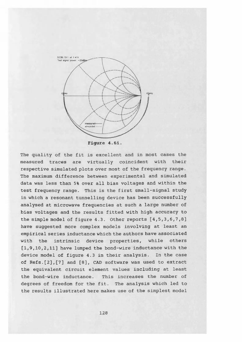
523B: S11 ot 1.41VTest signal power: -2 0 (
♦5MHziHz
simulated
Figure 4.6i.
The quality of the fit is excellent and in most cases the measured traces are virtually coincident with their respective simulated plots over most of the frequency range. The maximum difference between experimental and simulated data was less than 5% over all bias voltages and within the test frequency range. This is the first small-signal study in which a resonant tunnelling device has been successfully analysed at microwave frequencies at such a large number of bias voltages and the results fitted with high accuracy to the simple model of figure 4.3. Other reports [4,5,3,6,7,81 have suggested more complex models involving at least an empirical series inductance which the authors have associated with the intrinsic device properties, while others [1,9,10,2,11] have lumped the bond-wire inductance with the device model of figure 4.3 in their analysis. In the case of Refs.[2],[7] and [8], CAD software was used to extract the equivalent circuit element values including at least the bond-wire inductance. This increases the number of degrees of freedom for the fit. The analysis which led to the results illustrated here makes use of the simplest model
128
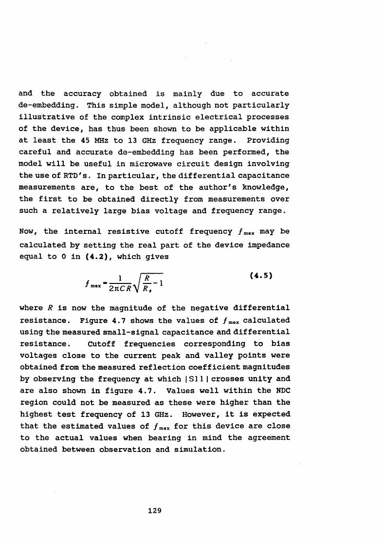
and the accuracy obtained is mainly due to accurate de-embedding. This simple model, although not particularly illustrative of the complex intrinsic electrical processes of the device, has thus been shown to be applicable within at least the 45 MHz to 13 GHz frequency range. Providing careful and accurate de-embedding has been performed, the model will be useful in microwave circuit design involving the use of RTD's. In particular, the differential capacitance measurements are, to the best of the author's knowledge, the first to be obtained directly from measurements over such a relatively large bias voltage and frequency range.
Now, the internal resistive cutoff frequency / m ax may becalculated by setting the real part of the device impedance equal to 0 in (4.2), which gives
where R is now the magnitude of the negative differential resistance. Figure 4.7 shows the values of / max calculated using the measured small-signal capacitance and differential
voltages close to the current peak and valley points were obtained from the measured reflection coefficient magnitudes by observing the frequency at which |S11 | crosses unity and are also shown in figure 4.7. Values well within the NDC region could not be measured as these were higher than the highest test frequency of 13 GHz. However, it is expected that the estimated values of fmax for this device are close to the actual values when bearing in mind the agreement obtained between observation and simulation.
max
(4.5)
resistance. Cutoff frequencies corresponding to bias
129
28N 26 O 24^ 22uc 20 0)=5 18cr
1 &4 —
4 —4 —O-t—1DUQ)>
calculatedmeasured
1.2 1.3 1.4- 0.9 1.0 1.11.3 1.2 1.1 - 1B ia s v o l t a g e / V
Figure 4.7 . Internal resistive cutoff frequency, / mtxlfor the RTD 523B as a function of bias voltage within the NDC region. The solid line was calculated from the extracted equivalent circuit parameters. The points represent the measured cutoff frequencies. It was not possible to obtain / max from the experimental data for bias voltages well within the NDC regions as these were outside the test frequency range.
4.2.1.4 Effects of test-signal power
Many authors have published results of small-signal microwave characterisation of resonant tunnelling devices, however, although the experimental methods employed were essentially similar to those reported here, some have unfortunately not
130
mentioned the test signal levels used [10,2,8,14,12], In fact, the effect of signal power on small-signal reflection measurements of RTD's has been all but overlooked in the literature. It will be shown here that considerations of test signal level are of the utmost importance and that these have a direct bearing on the accuracy of parameter extraction.
A digression is worthwhile at this point. The test signal power from the HP8510B used for the measurements described in section 4.2.1.1 was monitored over the test frequency range and found to fluctuate between about -22 and -25 dBm. The nominal power setting was -20 dBm and difficulties were experienced with phase locking when using lower signal levels. Ideally, as low a signal level as possible should be-employed, however, the nominal value of -20 dBm actually used proved to be sufficiently low.
The experimental procedure described in section 4.2.1.1 was repeated with a nominal signal level of -10 dBm (actually found to be between about -11 and -13 dBm) and using the same device. Subsequent analysis using the methods described in section 4.2 .1 . 2 revealed that it was impossible to extract frequency-independent parameter values at bias voltages close to regions were the I-V characteristic is highly nonlinear and within the NDC region. It was, however, found possible to obtain a relatively good fit to the experimental data at frequencies above about 4 GHz in most cases. Figure 4.8 shows some of the measured Sll traces plotted on Smith charts along with those calculated using the estimated parameter values derived from the analysis. In the cases where the bias voltage approached the NDC regions,
131
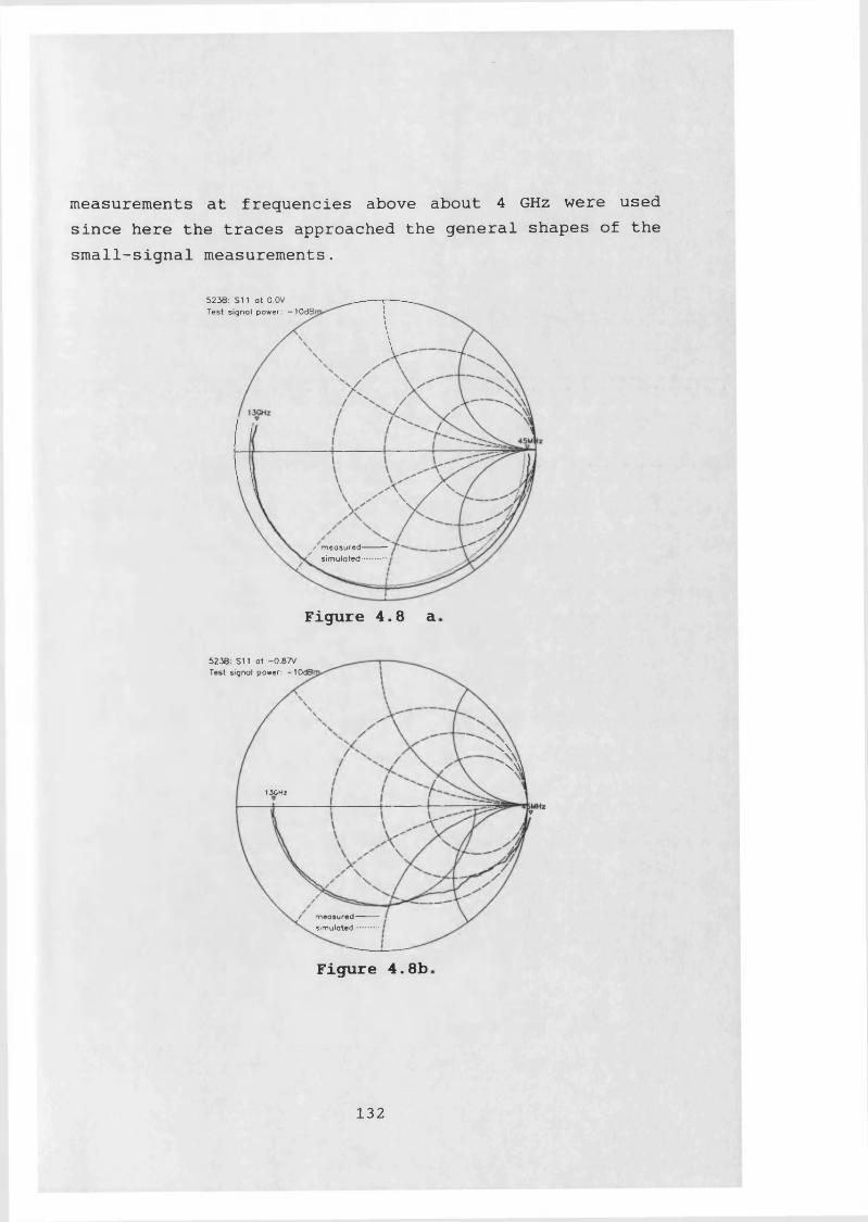
measurements at frequencies above about 4 GHz were used since here the traces approached the general shapes of the small-signal measurements.
5236: S11 ot 0.0V Test signal power: -10dBi
/ measured- simulated-
Figure 4.8 a
5238: S l l at -0 .87V Test signal power: -10dBi
\ V
\W \
13GHI
measured---------simulated —
Figure 4.8b
132
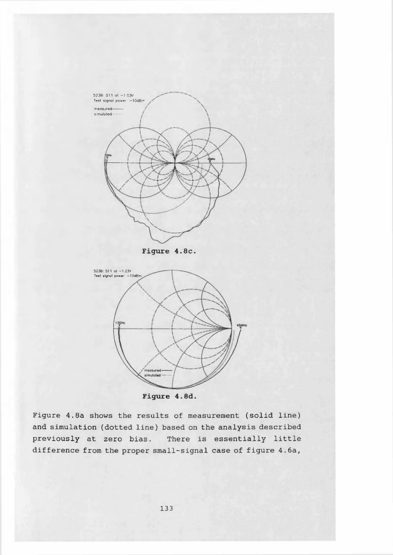
523B: S11 ot -1 .0 3 VTest signal power: -1 0 d B m
measured-simulated-
Figure 4.8c.
5238: S11 at -1.23V Test signal power: -10d6m
Figure 4.8d.
Figure 4.8a shows the results of measurement (solid line) and simulation (dotted line) based on the analysis described previously at zero bias. There is essentially little difference from the proper small-signal case of figure 4.6a,
133
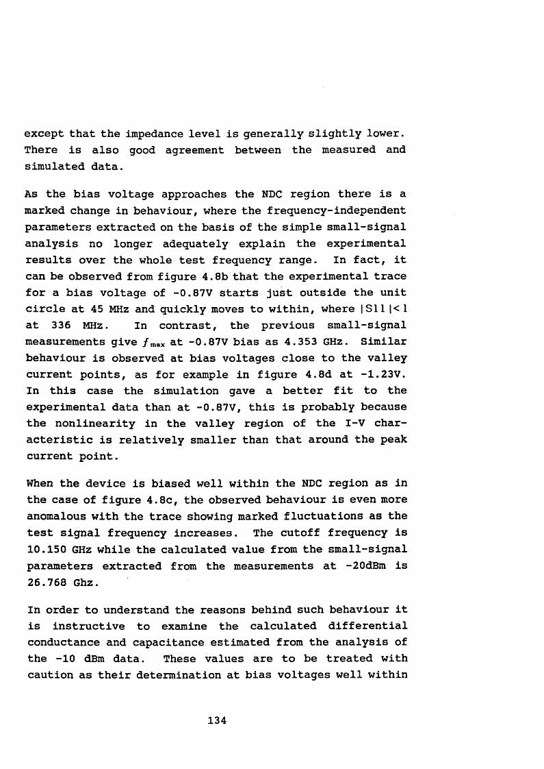
except that the impedance level is generally slightly lower. There is also good agreement between the measured and simulated data.
As the bias voltage approaches the NDC region there is a marked change in behaviour, where the frequency-independent parameters extracted on the basis of the simple small-signal analysis no longer adequately explain the experimental results over the whole test frequency range. In fact, it can be observed from figure 4.8b that the experimental trace for a bias voltage of -0.87V starts just outside the unit circle at 45 MHz and quickly moves to within, where | S 11 |< 1 at 336 MHz. In contrast, the previous small-signal measurements give / max at -0.87V bias as 4.353 GHz. Similar behaviour is observed at bias voltages close to the valley current points, as for example in figure 4.8d at -1.23V. In this case the simulation gave a better fit to the experimental data than at -0.87V, this is probably because the nonlinearity in the valley region of the I-V characteristic is relatively smaller than that around the peak current point.
When the device is biased well within the NDC region as in the case of figure 4.8c, the observed behaviour is even more anomalous with the trace showing marked fluctuations as the test signal frequency increases. The cutoff frequency is 10.150 GHz while the calculated value from the small-signal parameters extracted from the measurements at -20dBm is 26.768 Ghz.
In order to understand the reasons behind such behaviour it is instructive to examine the calculated differential conductance and capacitance estimated from the analysis of the -10 dBm data. These values are to be treated with caution as their determination at bias voltages well within
134
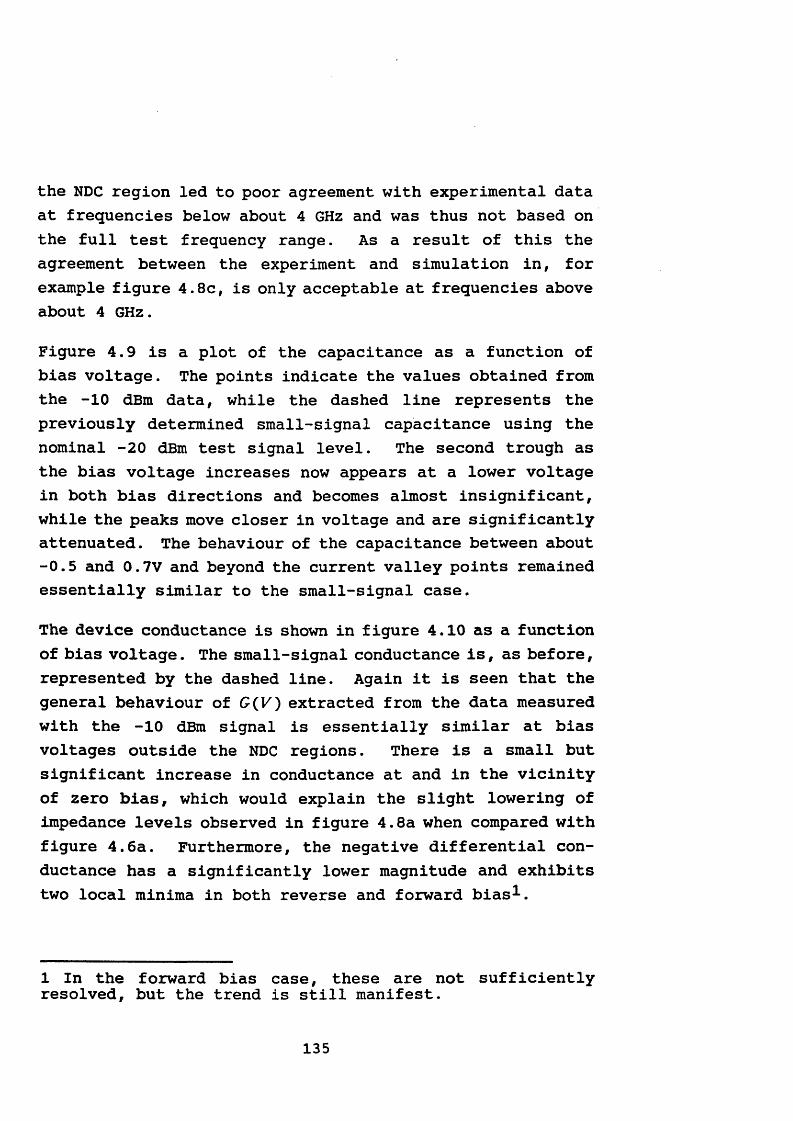
the NDC region led to poor agreement with experimental data at frequencies below about 4 GHz and was thus not based on the full test frequency range. As a result of this the agreement between the experiment and simulation in, for example figure 4.8c, is only acceptable at frequencies above about 4 GHz.
Figure 4.9 is a plot of the capacitance as a function of bias voltage. The points indicate the values obtained from the -10 dBm data, while the dashed line represents the previously determined small-signal capacitance using the nominal -20 dBm test signal level. The second trough as the bias voltage increases now appears at a lower voltage in both bias directions and becomes almost insignificant, while the peaks move closer in voltage and are significantly attenuated. The behaviour of the capacitance between about -0.5 and 0.7V and beyond the current valley points remained essentially similar to the small-signal case.
The device conductance is shown in figure 4.10 as a function of bias voltage. The small-signal conductance is, as before, represented by the dashed line. Again it is seen that the general behaviour of G(K) extracted from the data measured with the -10 dBm signal is essentially similar at bias voltages outside the NDC regions. There is a small but significant increase in conductance at and in the vicinity of zero bias, which would explain the slight lowering of impedance levels observed in figure 4.8a when compared with figure 4.6a. Furthermore, the negative differential conductance has a significantly lower magnitude and exhibits two local minima in both reverse and forward bias1 .
1 In the forward bias case, these are not sufficiently resolved, but the trend is still manifest.
135
0.4- 1 0 dBm test signal
- 2 0 dBm test signal0.380.36
P- 0.340.320.3
8" 0.280.260.240.22
-2 21 0 1B ia s v o l t a g e / V
Figure 4.9 . Capacitance of the 523B as a function of bias voltage. The points represent the values obtained from measurements with a -10 dBm test signal level, while the dashed line represents the small-signal capacitance of the same device obtained from measurements with a nominal -20 dBm signal level.
The cutoff frequencies have been markedly reduced, mainly as a result of the lower NDC exhibited by the device at the higher test signal level. In fact, figure 4.11 shows that at most bias voltages in the NDC region, / max < 13 GHz. The more drastic reductions occurred with bias voltages in the reverse bias NDC region as here the magnitude of the NDC has been subjected to a relatively higher attenuation (figure 4.10). The reason for this effect becomes apparent when one considers that the NDC region is wider in forward bias than in reverse. Now, the test signal causes the instan-
136
taneous terminal voltage of the device to sweep over the I-V characteristic to an extent determined by the signal amplitude and the degree of impedance match at any particular frequency and bias voltage. With bias voltages approximately in the middle of the forward bias NDC region the voltage excursion brought about by the application of the test signal does not encounter regions where the conductance is significantly different from the small-signal case. However, with a narrower NDC region and nominally similar voltage sweeps during the rf cycle, it would be more likely for the instantaneous voltage to encounter regions of greatly reduced conductance magnitudes or even cross into positive differential conductance regions. This would account for the smaller NDC magnitudes obtained in reverse bias. The reasons for the local maxima in the NDC magnitude are not apparent and would require detailed large-signal analysis to establish whether these are a result of inaccurate modelling or genuine features.
137
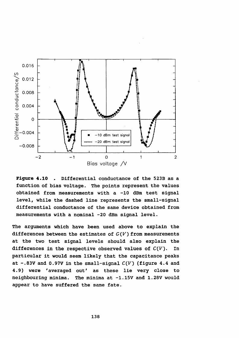
0.016co
0.012
0.008~oO 0.004o
-0.004■ —10 dBm test signol
— —20 dBm test signal-0.008
- 2 - 1 0 1 2Bias vo lta g e / V
Figure 4.10 . Differential conductance of the 523B as afunction of bias voltage. The points represent the values obtained from measurements with a -10 dBm test signal level, while the dashed line represents the small-signal differential conductance of the same device obtained from measurements with a nominal -20 dBm signal level.
The arguments which have been used above to explain the differences between the estimates of G(V) from measurements at the two test signal levels should also explain the differences in the respective observed values of C(K). In particular it would seem likely that the capacitance peaks at -.83V and 0.97V in the small-signal C(K) (figure 4.4 and 4.9) were 'averaged out' as these lie very close to neighbouring minima. The minima at -1.15V and 1.28V would appear to have suffered the same fate.
138
26
N 24S 22
ca lcu la ted
m easured
1.2 1.41.0- 1.3 - 0.91.1Bias vo lta ge / V
Figure 4.11 • Measured and calculated cutoff frequenciesof the 523B with a test signal level of -10 dBm. The missing points corresponding to bias voltages approximately in the middle of the forward bias NDC region correspond to values of / max > 13 GHz and thus outside the test frequency range.
The less significant capacitance maxima at -1.08V and -0.94 in reverse bias and 1.04V and 1.13V in forward bias coincide precisely with the anomalous minima in the respective NDC regions of figure 4.10, thus the two effects seem to be related. Evidence suggesting that these are genuine features may be obtained, at least for the reverse bias case, from figure 4.11 since the maxima in the measured / max also occur at -1.08 and -0.94V, and also correspond with those obtained by the calculation using the values of C(K) and G(K) extracted from the -10 dBm signal data.
139
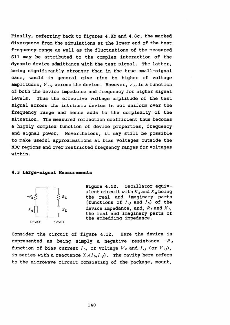
Finally, referring back to figures 4.8b and 4.8c, the marked divergence from the simulations at the lower end of the test frequency range as well as the fluctuations of the measured Sll may be attributed to the complex interaction of the dynamic device admittance with the test signal. The latter, being significantly stronger than in the true small-signal case, would in general give rise to higher rf voltage amplitudes, V r/, across the device. However, V rf is a function of both the device impedance and frequency for higher signal levels. Thus the effective voltage amplitude of the test signal across the intrinsic device is not uniform over the frequency range and hence adds to the complexity of the situation. The measured reflection coefficient thus becomes a highly complex function of device properties, frequency and signal power. Nevertheless, it may still be possible to make useful approximations at bias voltages outside the NDC regions and over restricted frequency ranges for voltages within.
4.3 Large-signal Measurements
Figure 4.12. Oscillator equivalent circuit with R d and X d being the real and imaginary parts(functions of /r/ and 70) of thedevice impedance, and, R L and X Ltthe real and imaginary parts of the embedding impedance.
Consider the circuit of figure 4.12. Here the device is represented as being simply a negative resistance -Rd function of bias current 10, or voltage V 0 and /r/ (or V r/), in series with a reactance X d{I0tIrf). The cavity here refersto the microwave circuit consisting of the package, mount,
DEVICE CAVITY
140
etc. which loads the device with an embedding impedance (Rl + jX l)* A basic requirement for a negative resistance oscillator active element is that at low Irf the magnitude of the negative resistance (/?d) must exceed the real part of the embedding impedance (RL). Thus, the net resistance in the circuit is negative and noise currents grow exponentially at a frequency determined by the reactive match of X L and X d. As the peak Irf grows, R d > R L until the net circuit resistance becomes zero and steady-state oscillations ensue. Thus, stable oscillations require the device negative resistance magnitude to fall with increasing /r/. So, the initial condition for the onset of oscillation is
R d(sma 11-signal) > R L (4.6)
when
X d(small-signal) = - X L (4.7)
and the final condition for stable oscillation is
*d(/o./r,) = Rl
In general the device reactance varies with Irf such that the oscillation frequency shifts until Ir/ stabilises.
At steady-state oscillation, the power made available by the device is given by
1 2 (4.9)P - ~lr,R*
141
assuming sinusoidal oscillations, where Irf is the peak rf current.
From the above brief discussion one concludes that device large-signal impedance (or admittance) must be determined as a function of bias voltage, rf signal power and frequency, and that this information is consequential in any subsequent attempt at designing prototype microwave circuits for large-signal operation. The procedure for such measurements will now be outlined.
Various workers have used basically similar techniques for large-signal device impedance or admittance measurements[13,14,15] in that having first de-embedded the device by some means, the device is biased into oscillation at a convenient power and frequency. The conjugate admittance of the matching network is then measured with a network analyser which thus determines the large-signal device impedance or admittance. The method presented here was implemented using packaged RTD's and follows the same general outline. Consider the arrangement represented schematically in figure 4.13.
The device is suitably mounted in a microwave package (E3 or E10/A in this case) and placed in a coaxial mount such as the ones described in chapter 3. It is then biased in the negative conductance region and the double-stub tuner (Maury Microwave™ model 2640D) adjusted for a convenient rf power output and frequency. These are measured on the spectrum analyser.
The mount, which is designed to be compatible with the test port connector on the network analyser reflection test unit, is removed and the rest of the circuit connected to the network analyser at reference plane AA' . The admittance
142
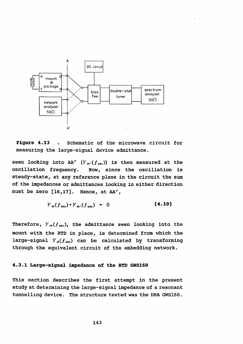
DC circuit
biasTee
package
m ount
double—stub
tuner
spectrumanalyser
50f)networkanalyser500
A'
Figure 4.13 . Schematic of the microwave circuit formeasuring the large-signal device admittance.
seen looking into AA' (Ym'C/o»e)) is then measured at the oscillation frequency. Now, since the oscillation is steady-state, at any reference plane in the circuit the sum of the impedances or admittances looking in either direction must be zero [16,17]. Hence, at AA',
^m(/«c)+ r m-U„c) - 0 (4.10)
Therefore, Y m(fosc), the admittance seen looking into themount with the RTD in place, is determined from which the large-signal y d(/„c) can be calculated by transforming through the equivalent circuit of the embedding network.
4.3.1 Large-signal impedance of the RTD 6HS160
This section describes the first attempt in the present study at determining the large-signal impedance of a resonant tunnelling device. The structure tested was the DRA GWS160.
143
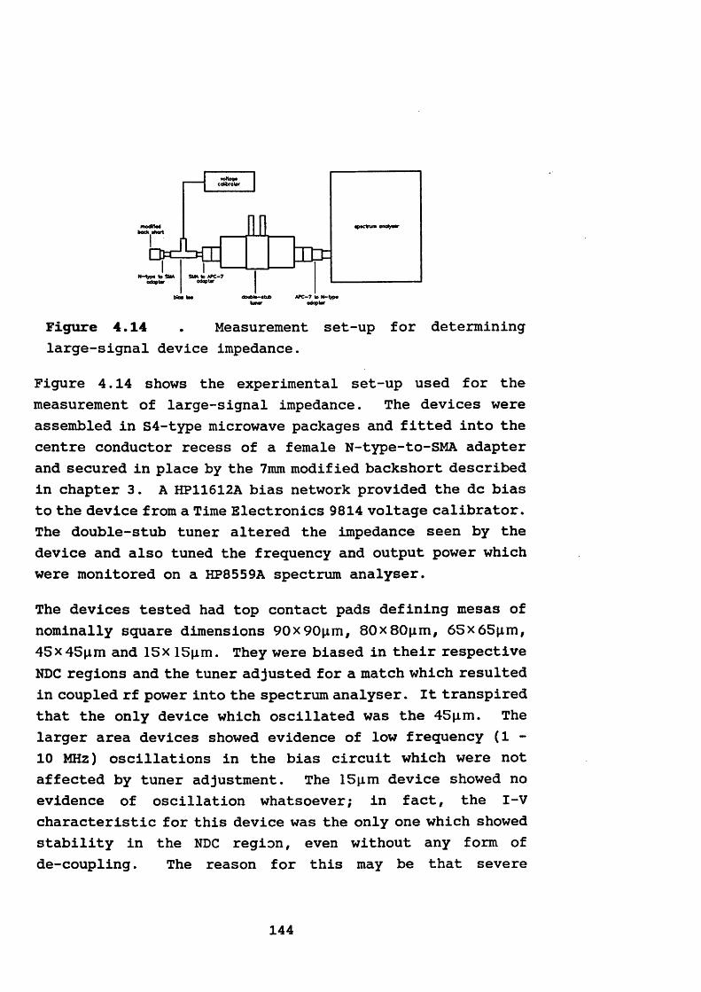
•p«ctrum oncfymr
APC-7 to N-typ* od^tir
Figure 4.14 . Measurement set-up for determininglarge-signal device impedance.
Figure 4.14 shows the experimental set-up used for the measurement of large-signal impedance. The devices were assembled in S4-type microwave packages and fitted into the centre conductor recess of a female N-type-to-SMA adapter and secured in place by the 7mm modified backshort described in chapter 3. A HP11612A bias network provided the dc bias to the device from a Time Electronics 9814 voltage calibrator. The double-stub tuner altered the impedance seen by the device and also tuned the frequency and output power which were monitored on a HP8559A spectrum analyser.
The devices tested had top contact pads defining mesas of nominally square dimensions 90x90|im, 80x80nm, 65x65iim, 45x45nm and 15x ISpim. They were biased in their respective NDC regions and the tuner adjusted for a match which resulted in coupled rf power into the spectrum analyser. It transpired that the only device which oscillated was the 45jxm. The larger area devices showed evidence of low frequency ( 1 - 10 MHz) oscillations in the bias circuit which were not affected by tuner adjustment. The 15p.m device showed no evidence of oscillation whatsoever; in fact, the I-V characteristic for this device was the only one which showed stability in the NDC region, even without any form of de-coupling. The reason for this may be that severe
144
undercutting during the wet chemical etch might have resulted in a very small-area device which is intrinsically stable at both dc and microwave frequencies (see chapter 2). The peak current density (assuming the nominal device area) for this device was found to be ~ 9 A c m ' 2, much smaller than that of the others (400-700Acm"2).
Thus, the microwave measurements described above could only be performed on the 45p.m device. Hence, with this device in the modified mount and using the configuration of figure4.14, a forward bias voltage was set in the middle of the NDC region at 0.709V. The tuner was then adjusted to obtain the lowest oscillation frequency allowable. This was 810 MHz at about -13 dBm. The tuner adjustments were then noted. The output frequency was subsequently increased in approximately 50 MHz steps up to 1.13 GHz (the highest oscillation frequency obtainable), each time keeping output power approximately constant and noting the tuner adjustments. Higher power levels (about -lOdBm) were achievable but could not be maintained constant over the tuning range. The fact that the output was so low may invalidate the claim for large-signal measurements, but nevertheless the procedure is still applicable.
The device was then removed from the mount and the spectrum analyser replaced by a 50 0 termination. Single frequency impedance measurements were then made by connecting the unknown port of a HP8410A network analyser to the N-type female-to-SMA adapter such that the reference plane coincided with the device position. The tuner settings which resulted in the stable oscillation conditions determined above were replicated and the impedance looking towards the tuner from the package plane was measured for each setting.
145
4.3.1.1 Some important observations
The oscillations observed were strongly effected by tuner adjustments. Moving the tuner stubs out by more than about 1mm resulted in spurious oscillations in the bias circuit which were not effected by tuner adjustments. The spectrum of these oscillations could not be observed on the spectrum analyser as the lower cutoff frequency of the bias network was 45 MHz. However, these oscillations were examined by connecting a wide-bandwidth oscilloscope across the dc circuit and found to have waveforms similar to relaxation oscillations as discussed in chapter 2. The frequency of these spurious oscillations was between about 500 kHz and 5 MHz and depended strongly on the applied bias.
Moving the tuner stubs back in resulted in a dramatic change in the output spectrum in that single frequency oscillations appeared suddenly at frequencies tuneable between about 800 MHz to just over 1 GHz. This spectrum consisted of a fundamental within this frequency range at a power level of about -13dBm with harmonics the highest of which was less than 30dB below the fundamental. The bandwidth was about 50 kHz.
The most important observation was that the bias circuit oscillations disappeared instantly with the onset of the single-frequency oscillations. To the best of the author's knowledge and at the time of writing, this is the first time that such observations have been reported in respect of resonant tunnelling devices. Indeed, with all oscillating devices tested during the course of this study, the bias circuit oscillations have been observed to disappear (outside measurable limits) irrespective of any de-coupling circuit on the dc arm as soon as the conditions for a well-defined
146
microwave spectrum with clearly discernible oscillations have been established1 . The implications of this effect on high- and moderately high-Q potential applications would mean that dc and low-frequency stabilisation design would be greatly simplified; a significant advantage since RTD's are notoriously difficult to stabilise at low frequencies.
4.3.1.2 Results and Analysis
In a freely-running oscillator circuit generating a stable rf output, the sum of the impedances looking into either side of any reference plane along the circuit must be zero [18] . Thus, if the measured impedance at the packaged device plane is Z m, then the impedance of the embedded device (i.e., including package and mount parasitic effects), Z amb, may be obtained from
Z m + Z.mb-0 (4.11)
At this point, the device impedance may be de-embedded by transforming Z #mb through an appropriate equivalent circuit model for the package and mount combination. As the equivalent circuit due to Owens [19] is currently the best-available model for this package and mount combination, it was used to determine the device impedance at all test frequencies. The only parameter value changed was that due to the bonding wire inductance. The bonding wire stretches diametrically across the package flange and is bonded to the device top contact roughly at the middle of its length. This suggests an equivalent circuit for the lead inductance
1 See Appendix IV for examples of microwave spectral output of some of the tested devices.
147
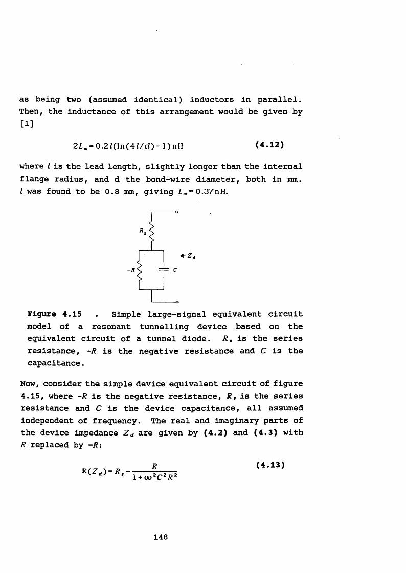
as being two (assumed identical) inductors in parallel. Then, the inductance of this arrangement would be given by [1]
2LW = 0.2 Z(ln (4 Z/d)- 1) nH (4.12)
where I is the lead length, slightly longer than the internal flange radius, and d the bond-wire diameter, both in mm. Z was found to be 0.8 mm, giving 0.37nH.
Figure 4.15 . Simple large-signal equivalent circuitmodel of a resonant tunnelling device based on the equivalent circuit of a tunnel diode. R, is the series resistance, -/? is the negative resistance and C is the capacitance.
Now, consider the simple device equivalent circuit of figure4.15, where -/? is the negative resistance, R, is the series resistance and C is the device capacitance, all assumed independent of frequency. The real and imaginary parts of the device impedance Z d are given by (4.2) and (4.3) with R replaced by -/?:
o
-o
R (4.13)1 + uo2C zR 2
148
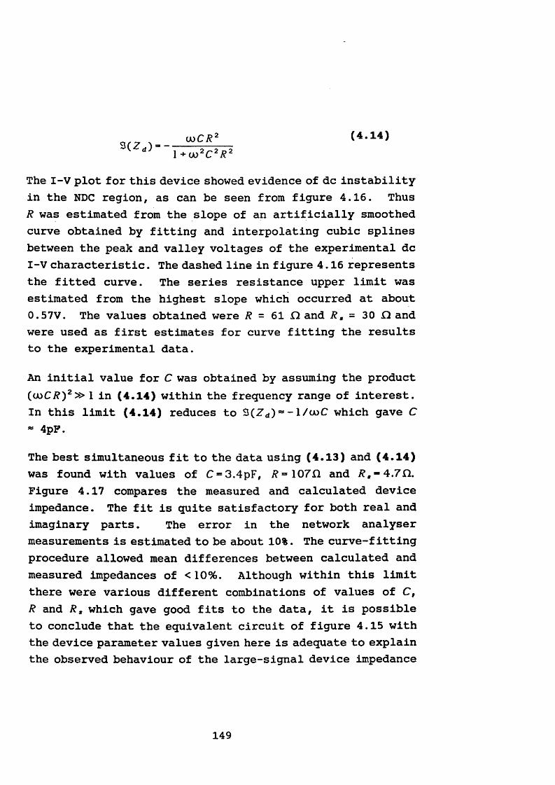
The I-V plot for this device showed evidence of dc instability in the NDC region, as can be seen from figure 4.16. Thus R was estimated from the slope of an artificially smoothed curve obtained by fitting and interpolating cubic splines between the peak and valley voltages of the experimental dc I-V characteristic. The dashed line in figure 4.16 represents the fitted curve. The series resistance upper limit was estimated from the highest slope which occurred at about 0.57V. The values obtained were R = 61 Cl and R, = 30 Cl and were used as first estimates for curve fitting the results to the experimental data.
An initial value for C was obtained by assuming the product (u>C/?)2» l in (4.14) within the frequency range of interest. In this limit (4.14) reduces to 3(Zd) ~ - 1/ooC which gave C - 4pF.
The best simultaneous fit to the data using (4.13) and (4.14) was found with values of C = 3.4pF, /?=107H and /?,-4.7n. Figure 4.17 compares the measured and calculated device impedance. The fit is quite satisfactory for both real and imaginary parts. The error in the network analyser measurements is estimated to be about 10%. The curve-fitting procedure allowed mean differences between calculated and measured impedances of <10%. Although within this limit there were various different combinations of values of C, R and R s which gave good fits to the data, it is possible to conclude that the equivalent circuit of figure 4.15 with the device parameter values given here is adequate to explain the observed behaviour of the large-signal device impedance
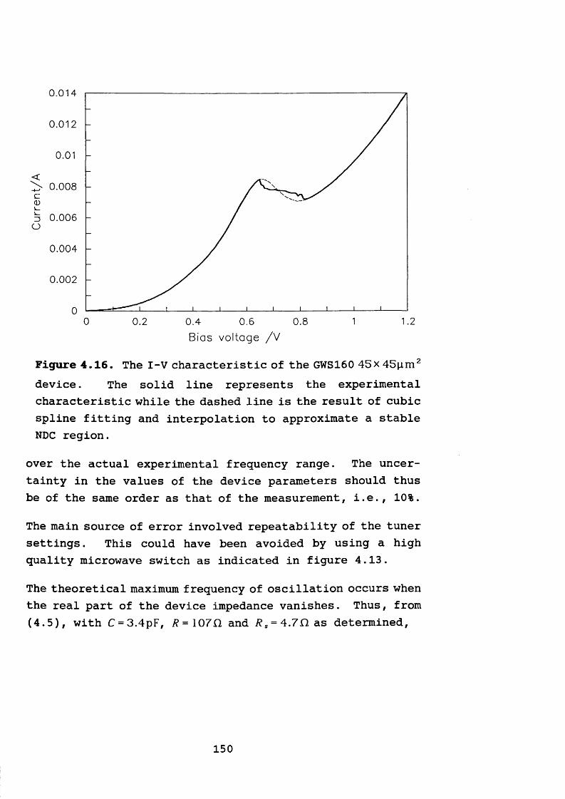
0.014
0.012
0.01
<-t—' 0.008c<DZ3 0.006o
0.004
0.002
0 . -t------- i_______________i___________i___________ i___________ i___________ i___________ i----------- 1----------- 1----------- 1-----------
0 0.2 0.4 0.6 0.8 1 1.2Bias voltage /V
Figure 4.16. The I-V characteristic of the GWS160 45 x 4 5 p m 2
device. The solid line represents the experimental characteristic while the dashed line is the result of cubic spline fitting and interpolation to approximate a stable NDC region.
over the actual experimental frequency range. The uncertainty in the values of the device parameters should thus be of the same order as that of the measurement, i.e., 1 0 %.
The main source of error involved repeatability of the tuner settings. This could have been avoided by using a high quality microwave switch as indicated in figure 4.13.
The theoretical maximum frequency of oscillation occurs when the real part of the device impedance vanishes. Thus, from (4.5), with C = 3.4pF, R = 107C and /?s = 4.70 as determined,
150
- 1 0
JZ - 2 0
measured real part
measured imag. part- 3 0
Q .
- 4 0
- 5 0
1.120.8 0.88 1 . 0 40 . 9 6
frequency /GHz
Figure 4.17 . Large-signal impedance of the 45M./72 deviceas a function of frequency. The curves are fitted to the data on the basis of the equivalent circuit model of figure 4.15, with C = 3.4pF, /?=107O, R s-4.70 and a bonding wire inductance of 0.37nH.
fmax is about 2 GHz. As this is an intrinsic device limit to the oscillation frequency based on measurements at -13 dBm, it is in reasonably good agreement with observation.
Finally, having obtained an estimate of the device impedance, the voltage amplitude across the actual device can be estimated assuming purely sinusoidal oscillations from
_ IKpl2 (4.15)ou‘ " 2S(-Zd)
where Pou/= -13dBm is the output power. This leads to a valueof V 0 between about 45 and 30mV. One can thus understand, at least qualitatively, the reason for the difference between the differential resistance estimate from the dc characteristic and the value obtained by curve-fitting the rf
151
data. The bias point chosen for the impedance measurements coincides with the point where the negative differential resistance has the lowest magnitude of 61 D, from the spline-fitted line of figure 4.16. During the oscillation cycle the instantaneous bias point is swept by about ± K 0 from the dc value, the oscillations about this point thus smear out the minimum value of R shifting it to higher values.
4.3.2 Large-signal impedance of the RTD 523B
The configuration used for the measurements was similar to the one of figure 4.14 but, in this case, the 3.5mm mount described in chapter 3 was used in order to house the E10/A package and a HP8593A spectrum analyser in place of the HP8559A. The measurement procedure was the same as described in section 4.2.1, however the network analyser used to measure the impedance looking into the tuner from the package plane was a HP8510B. This was calibrated using standard open and short circuits, a standard fixed load and a sliding load.
The harmonics observed were more than 20 dB below the fundamental, thus the oscillations were practically single frequency. Tuner adjustments were made to obtain a power level of -8.4 dBm at frequencies spaced by about 33 MHz between 2.149 and 3.403 GHz at a bias voltage of 1.30V.
For practical reasons it was not possible to employ a microwave switch as shown in figure 4.13 in order to avoid errors introduced by lack of accurate repeatability of the tuner settings for the impedance measurements.
152
4.3.2.1 Observations
The output spectrum from this device was similar in nature to that of the GWS160. However, the fundamental frequency could be tuned between about 2 and 4 GHz and maximum power levels of about -7 dBm were achieved with a voltage bias of 1.30V. The strongest harmonic observed was the third and this was less than 20 dB below the fundamental.
As the tuner stub assembly is moved, say towards the device, the output frequency increases linearly with the position of the stub assembly until at some point a mode hop occurs resulting in a sudden shift with the fundamental at a lower frequency and several harmonics. The original spectrum could be retrieved by moving the stub assembly well back, extracting the stubs by about 2 mm and pushing them back in. This is due to tuning hysteresis.
Mode hops were sometimes observed to occur of their own accord when the above-mentioned tuner settings were approached but not surpassed.
Bias circuit oscillations were confirmed to be relaxation oscillations and again observed to disappear instantly with the advent of sharp spectral lines at microwave frequencies.
4.3.2.2 Results and Analysis
The measured impedances looking towards the tuner from the package plane were transformed through the E10/A package- mount model established in chapter 3. Thus, the resulting impedances give - Z d(/).
153
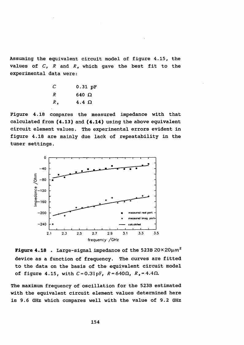
Assuming the equivalent circuit model of figure 4.15, the values of C, R and R s which gave the best fit to the experimental data were:
C 0.31 pFR 640 DR s 4.4 D
Figure 4.18 compares the measured impedance with that calculated from (4*13) and (4.14) using the above equivalent circuit element values. The experimental errors evident in figure 4.18 are mainly due lack of repeatability in the tuner settings.
o
-4 0
o -so-1 2 0
-200 measured real port -
measured imog. part-
-240 - ♦3.53.33.12.1 2.3 2.7 2.92.5
frequency /GHz
Figure 4.18 . Large-signal impedance of the 5 2 3B20x20nm2 device as a function of frequency. The curves are fitted to the data on the basis of the equivalent circuit model of figure 4.15, with C = 0.31pF, /? = 640fl, tf,*4.4n.
The maximum frequency of oscillation for the 523B estimated with the equivalent circuit element values determined here is 9.6 GHz which compares well with the value of 9.2 GHz
154
obtained by interpolating between the measured points in figure 4.11 of section 4.2.1.4 at 1.30V. However, the highest observed frequency was 4.2 GHz with an output power of -9 dBm. This is probably due to limitations of the tuning arrangement which did not allow it to support such high frequencies.
Applying (4.15) and with values of C, R and R s as determined, it is possible to conclude that the rf voltage amplitude across the device was between about 150 and 90mV over the test frequency range.
The stable I-V characteristic of this device, shown in figure 4.1, gives the differential resistance magnitude at dc as 250 flat 1.30V bias. The fitted large-signal value was 640 D. Now, the differential conductance tends to zero as the voltage approaches 1.43V. Thus the voltage amplitude, as has been determined, would sweep the instantaneous voltage across the device into regions where the differential resistance greatly exceeds 250 D in magnitude and may even cross over into regions where this becomes positive. The average value of R during the cycle therefore increases.
Since the device capacitance is also voltage-dependent, it would behave in a similar way and one would expect the low frequency small-signal value to be considerably different from that determined from the large-signal measurements. In this case the small-signal capacitance was found to be0.25pF at 1.30V from the results of section 4.2.1.2.
4.4 Summary of the main results and conclusions
The simple tunnel diode equivalent circuit has been applied to analyse the small-signal microwave properties of the RTD
155
523B. Results show that simulations based on this model are in excellent agreement with the experimental results. The device differential conductance and capacitance extracted by fitting this model to the small-signal admittance measurements are f requency-independent, at least up to 13 GHz, and will be useful in large-signal analysis.
The effect of signal power upon such measurements has also been investigated. It was shown that using a signal level of about -10 dBm gives results that cannot be accurately predicted by the model, especially with bias voltages within the NDC regions and over wide frequency ranges.
Impedance measurements on the GWS160 and 523B RTD's in a simple microwave oscillator circuit have confirmed that the use of this device equivalent circuit can be extended to the large-signal case with the conductance and capacitance values used being functions of bias voltage and rf output power. It was also observed that dc stability is not an important consideration when RTD's are used in high- or moderately high-Q cavities because when the devices are biased to oscillate and the impedance presented by the cavity is such as to support narrow bandwidth microwave oscillations, spurious oscillations in the bias line disappear.
156
References1. T. J. Shewchuk, P. C. Chapin, J. M. Gering, P. D. Coleman, W. Kopp, and H. Morkog, "Microwave admittance characterisation of GaAs-AlxGai_xAs resonant tunneling heterostructures 11 , Proceedings of the IEEE: Cornell Conference on advanced concepts in high speed semiconductor devices and circuits, Cornell University, Ithaca, New York, 1985, pp. 370-379.2. J. M. Owens, D. J. Halchin, K. L. Lear, W. S. Lee, and J. S. Harris Jr., "Microwave characteristics of MBE grown resonant tunneling devices", IEEE International Microwave Symposium Digest, 1989, pp. 471-474.3. A. Zarea, A. Sellai, M. S. Raven, D. P. Steenson, J. M. Chamberlain, M. Henini, and 0. H. Hughes, "Small signal analysis of resonant tunnel diodes in the bistable mode", in W. Eccleston and P. J. Rosser, (ed.), ESSDERC 90, 20th European Solid State Device Research Conference, Nottingham, IOP Publishing Ltd, 1990, pp. 559-562.4. J. M. Gering, D. A. Crim, D. G. Morgan, and P. D. Coleman, "A small-signal equivalent-circuit model for GaAs-AlxGai_xAs resonant tunneling heterostructures at microwave frequencies", J. Appl. Phys., Vol. 61, 1987, pp. 271-276.5. J. M. Gering, T. J. Rudnick, and P. D. Coleman, "Microwave detection using the resonant tunneling diode", IEEE Trans Microwave Theory Tech., Vol. MTT-36, 1988, pp. 1145-1150.6 . A. Zarea, A. Sellai, M. S. Raven, D. P. Steenson, J. M. Chamberlain, M. Henini, andO. H. Hughes, "Impedance analysis of GaAs/Al(Ga)As resonant tunnelling diodes in the NDR region", Electron. Lett., Vol. 26, 1990, pp. 1522-1523.7. R. E. Miles, G. Millington, R. D. Pollard, D. P. Steenson, J. M. Chamberlain, and M. Henini, "An accurate equivalent circuit model of resonant tunnelling diodes", Electron. Lett., Vol. 27, 1991, pp. 427-428.8 . M. F. C. Schemmann, H. C. Heyker, J. J. M. Kwaspen, andTh. G. Van de Roer, "Microwave impedance measurements on resonant tunnelling diodes and network model parameter extraction", IEE Proc.-H, Vol. 138, 1991, pp. 248-252.9. E. R. Brown, W. D. Goodhue, and T. C. L. G. Sollner, "Fundamental oscillations up to 200 GHz in resonant tunneling diodes and new estimates of their maximum oscillation frequency from stationary-state tunneling theory", J. Appl. Phys., Vol. 64, 1988, pp. 1519-1529.10. D. Lippens and P. Mounaix, "Small-signal impedance ofGaAS-AlxGai_xAs resonant tunnelling heterostructures at microwave frequencies", Electron. Lett., Vol. 24, 1988, pp. 1180-1181.
157
11. P. Mounaix, P. Bedu, and D. Lippens, "Measurement of negative differential conductance to 40 GHz for vertically integrated resonant tunnelling diodes", Electron. Lett., Vol. 27, 1991, pp. 1358-1359.12. A. Zarea, M. S. Raven, D. P. Steenson, J. M. Chamberlain, M. Henini, and 0. H. Hughes, "Effect of temperature on frequency limits of GaAS/AlGaAs resonant tunnel diodes", Electron. Lett., Vol. 28, 1992, pp. 264-266.13. D. R. Decker, C. N. Dunn, and R. L. Frank, "Large-signal silicon and germanium avalanche diode characteristics", IEEE Trans. Microwave Theory Tech., Vol. MTT-18, 1970, pp.872-876.14. J. McBretney and M. J. Howes, "Electrical characterisation of transferred electron devices by a novel galva- nomagnetic technique", IEEE Trans. Microwave Theory Tech., Vol. MTT-27, 1979, pp. 256-265.15. P. D. Coleman, S. Geodeke, T. J. Shewchuk, and P. C. Chapin, "Experimental study of the frequency limits of a resonant tunneling oscillator", Appl. Phys. Lett., Vol. 48, 1986, pp. 422-424.16. K. Kurokawa, "Some basic characteristics of broadband negative resistance oscillator circuits", Bell Syst. Tech. J., Vol. 48, 1969, pp. 1937-1955.17. W. F. Chow, "Principles of Tunnel Diode Circuits," John Wiley & Sons, Inc., London, 1964.18. K Kurokawa, "Microwave Solid State Oscillator Circuits", in M. J. Howes and D. V. Morgan (ed.),"Microwave Devices: Device Circuit Interactions", John Wiley & Sons, 1976.19. R. P. Owens, "Mount-independent equivalent circuit of the S4 diode package", Electron. Lett., Vol. 7, 1971, pp. 580-582.
158
CHAPTER 5
LARGE-SIGNAL ANALYSIS OF A SIMPLE RTD MULTIPLIER
5.1 Introduction
A nonlinear impedance driven by a periodic source (the pump) gives rise to frequency multiplication. The main types of millimetre wave harmonic generators utilise either the nonlinear resistance of a forward biased Schottky barrier diode or the nonlinear capacitance of a reverse biased varactor diode.
Resistive multipliers have been in use since the early 1940's [1]. Since then, many workers have reported resistive diode multipliers operating in the millimetre-wave region with useful output powers [2,3,4,5,6,7,8,9,10,11,12]. The conversion efficiency for generating the nth harmonic of a resistive multiplier is fundamentally limited to n~2[13,14,15]. In contrast, the Manley-Rowe relations [16] predict no limit below 1 0 0 % efficiency for nonlinear reactance multipliers. The high efficiency of varactor multipliers has therefore made them attractive for use in solid state microwave power sources at frequencies up to about 100 GHz.
However, varactor multipliers have an inherent frequency limitation caused by the saturation velocity of the neutral space-charge boundary. At frequencies above about 100 GHz the usable nonlinearity of the transition capacitance diminishes because the carrier velocity in the space-charge layer cannot exceed the saturation velocity [17]. Hence, despite the excellent performance of some early varactor multipliers in the microwave region [18,19,20] the efficiencies of devices in the millimetre-wave band fell far below the levels predicted by theory [21]. It was not until quite recently that millimetre-wave reactive multipliers
159
began to achieve respectable output power levels and much of the improvement was due to advances in diode fabrication technology. Some recent state-of-the-art nonlinear reactance multipliers have found use as local oscillators in millimetre-wave mixers and heterodyne receivers where hitherto expensive and short-lived klystrons had been used. For example, Archer [22] reported a doubler exhibiting typically 1 0 % conversion efficiency at an output frequency range of 100-260 GHz and a tripler at 215 GHz with 6 % efficiency. Erickson [23] obtained a peak 6 % efficiency at 266 GHz. Recently, a novel submillimetre wave tripler using a quantum-barrier-varactor diode [24] resulted in 5% conversion efficiency between 210 and 280 GHz and a quintupler efficiency of just below 0.2% at 310 GHz, comparable to state-of-the-art Schottky diode quintuplers.
5.2 Frequency multiplication with resonant tunnelling devices
5.2.1 Odd harmonic multiplier
The I-V curve of a RTD may be represented by a polynomial such as [25]
((v) = X a 2„_,u2"'1n« 1
a l = 0.32mAV~1
a 3 = 8 .2 m A V ‘3
a 5 = - 124mA V '5
a7 = 403 m A V ~ 7
Suppose for simplicity we assume a purely sinusoidal pump voltage v = v0cosuot. Then, substituting for v in (5.1) and simplifying gives the time-dependent current in the RTD as
(5.1)(v < 0.5 V)
160
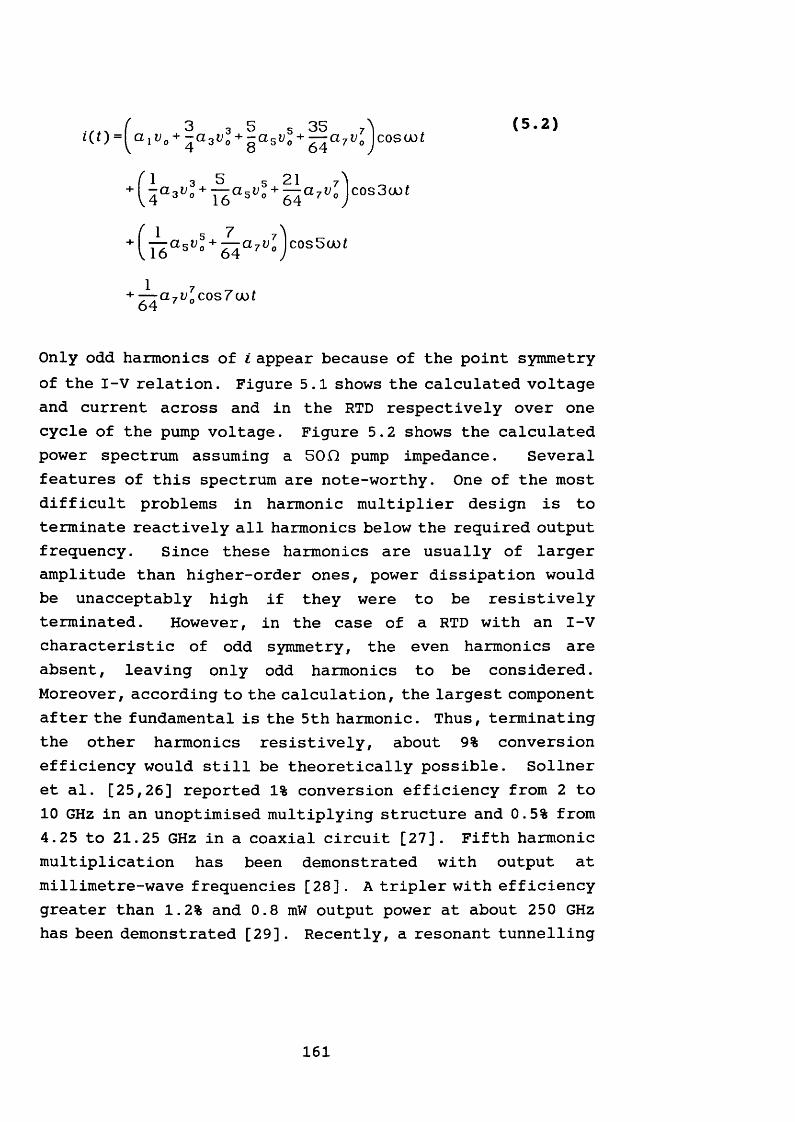
Only odd harmonics of i appear because of the point symmetry of the I-V relation. Figure 5.1 shows the calculated voltage and current across and in the RTD respectively over one cycle of the pump voltage. Figure 5.2 shows the calculated power spectrum assuming a 50D pump impedance. Several features of this spectrum are note-worthy. One of the most difficult problems in harmonic multiplier design is to terminate reactively all harmonics below the required output frequency. Since these harmonics are usually of larger amplitude than higher-order ones, power dissipation would be unacceptably high if they were to be resistively terminated. However, in the case of a RTD with an I-V characteristic of odd symmetry, the even harmonics are absent, leaving only odd harmonics to be considered. Moreover, according to the calculation, the largest component after the fundamental is the 5th harmonic. Thus, terminating the other harmonics resistively, about 9% conversion efficiency would still be theoretically possible. Sollner et al. [25,26] reported 1% conversion efficiency from 2 to 10 GHz in an unoptimised multiplying structure and 0.5% from 4.25 to 21.25 GHz in a coaxial circuit [27]. Fifth harmonic multiplication has been demonstrated with output at millimetre-wave frequencies [28] . A tripler with efficiency greater than 1.2% and 0.8 mW output power at about 250 GHz has been demonstrated [29]. Recently, a resonant tunnelling
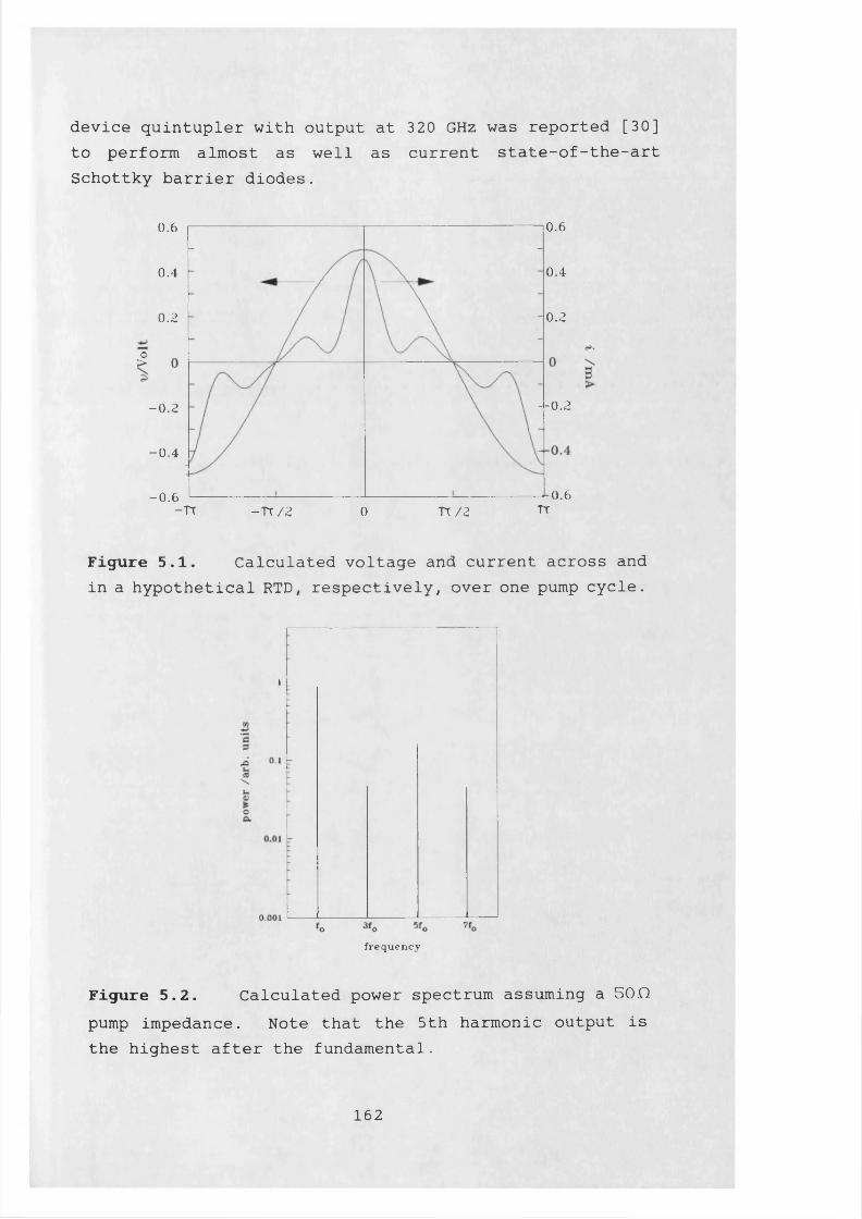
device quintupler with output at 320 GHz was reported [30] to perform almost as well as current state-of-the-art Schottky barrier diodes.
0.60.6
0.40.4
0.20.2
o>
- - 0.2- 0.2
- 0 .4
0.6- 0.6TT-TT - T t / 2 0 T T /2
Figure 5.1. Calculated voltage and current across and in a hypothetical RTD, respectively, over one pump cycle.
1 r
f r e q u e n c y
Figure 5.2. Calculated power spectrum assuming a 50D pump impedance. Note that the 5th harmonic output is the highest after the fundamental.
162
5.2.2 Doubler
Suppose that a RTD is biased at the peak current voltage V pand a sinusoidal (pump) signal of frequency go with amplitude v0 is applied such that the excursion along the I-V characteristic over the pump cycle is V p±v0. If u0 is small enough, the relevant part of the I-V curve may be approximated by a parabola:
Kv) = + U P-1 o) 1 -
I 0 = i( 0)
- {KV±v0)-I
v-VV n
i - 4v p j
(5.3)
V
P± o) may be determined from the I-V curve. Substituting for v in (5.3) gives
<(0 = /o + (/p-/o) 1- _vl_2V] 2K| cos2cof (5.4)
Thus, the rf current in the RTD is also sinusoidal and has double the pump frequency. This simple analysis suggests that there is the potential of realising a frequency doubler based on the resonant tunnelling device. The attractive feature is that providing the pump amplitude is small enough, no harmonics are produced other than the second harmonic of the pump frequency, a fact which would greatly simplify its realisation.
The foregoing treatment completely neglects problems arising from the interaction of the pump signal and subsequent harmonics generated with the device parasitics and the embedding network. The signal power has to be effectively coupled from the input part of the circuit to the device and at the same time the harmonic of interest has to be coupled into another part of the circuit where it can be
163
utilised. Furthermore, the input and output circuits have to be effectively isolated from one another and a stable biasing arrangement designed to de-couple the dc and RF circuits over the entire operating frequency range.
In chapter 4, the influence of test signal power on microwave ref lection measurements of an active device was investigated. It was concluded that the device-circuit-signal interaction is highly complex. A self-consistent method of large-signal analysis is therefore required in order to understand and simulate the behaviour of a RTD in a multiplier circuit. The following sections describe in detail the multiple reflection technique [31] and show how this can be used in the analysis of a simple RTD multiplier configuration.
5.3 Multiplier analysis
The analysis of the performance of a frequency multiplier involves only large signals, unlike mixers where both small- and large-signal analyses have to be performed. However, the large-signal analysis of both configurations need not differ significantly. In the present work, therefore, the mixer approach, which has been developed sufficiently well, will be adopted. As with mixers, the most difficult step in analysing multipliers is precisely that of determining the diode waveforms produced by the pump (or local oscillator in the case of mixers). High diode nonlinearities, the distributed nature of the elements comprising the multiplier and device parasitics only complicate matters.
Torrey and Whitmer [32] describe one of the first attempts at solving the large signal problem. They obtained analytical solutions by assuming a sinusoidal voltage at the diode terminals, i.e. that no harmonic voltages were present beyond the local oscillator (LO) frequency. In their analysis, Torrey and Whitmer considered both a purely resistive diode and one represented by a nonlinear conductance shunted by
164
a constant capacitance. The more complicated variable capacitance case was only considered qualitatively. Later analyses [33,34,35,36] included quantitative treatments of nonlinear capacitance, although making the same simplifying assumption of a sinusoidal driving voltage. Barber [37] indicated the necessity for removing this constraint at the LO frequency.
Fieri and Cohen [38] performed large signal analysis in a very simple lumped element embedding network. In their approach a numerical Runge-Kutta integration algorithm was used to solve the network state equations for the time-dependent diode voltage and current. Gwarek [39] extended this method to allow more general embedding circuits. He represented the embedding network as a simple lumped element circuit in series with a set of voltage sources, one at each LO harmonic. The amplitudes and phases of these generators are adjusted to keep the terminal impedance of the circuit equal to that of the actual embedding network. Although the scheme works well for many mixer circuits, it is strongly dependent on the guessed values of the lumped elements and does not converge for all embedding impedances [40].
An early form of the harmonic balance technique was used by Egami [41] to find the terminal voltage and current waveforms for a diode with constant capacitance. The mixer equivalent circuit was separated into two parts, one containing the linear embedding network, and the other containing the nonlinear diode elements. The voltages and currents in each half were then matched (or balanced) at all the LO harmonic frequencies using an iterative procedure. In this approach, the linear circuit problem (i.e. the embedding circuit) is solved in the frequency domain while a time domain solution is sought for the state equations representing the nonlinear
165
circuit. This method seemed to be effective when one or two LO harmonics were considered, but convergence to a steady state proved difficult when more harmonics were included.
Gupta and Lomax [42] described a method for large signal analysis of IMPATT oscillators where a pair of dual algorithms are used to update the estimates of either the diode voltage or current after each iteration. Convergence was reached once a stationary solution was obtained by this self-consistent approach. Hicks and Khan [43,44] have reported excellent results with a generalisation of the Gupta and Lomax procedure. The Hicks and Khan algorithms have since been used successfully on a variety of nonlinear circuits.
The large signal analysis technique used in the present work was originally developed by Kerr [31] and subsequently used by Siegel, Kerr and Hwang [40] in Schottky mixer and varactor multiplier analysis. It solves the nonlinear problem by iterating over a series of reflection cycles of the voltage waveforms between the diode and the embedding network. Like the harmonic balance methods, the algorithm operates in the time domain when considering the diode and in the frequency domain when dealing with the embedding network. This multiple reflection technique requires more computing time than either the methods of Gwarek [39] or Hicks and Khan [43,44], but solutions were obtained for all mixer and multiplier circuits which were studied by Siegel, Kerr and Hwang [40].
5.3.1 The multiple reflection technique
The large signal equivalent circuit of a nonlinear reactance multiplier is represented in figure 5.3. The intrinsic device is, as before, represented by a nonlinear conductance g(vd) shunted by a nonlinear capacitance c(t»d), where vd is the instantaneous voltage across the intrinsic device. The device series resistance, R sr will here be assumed inde
166
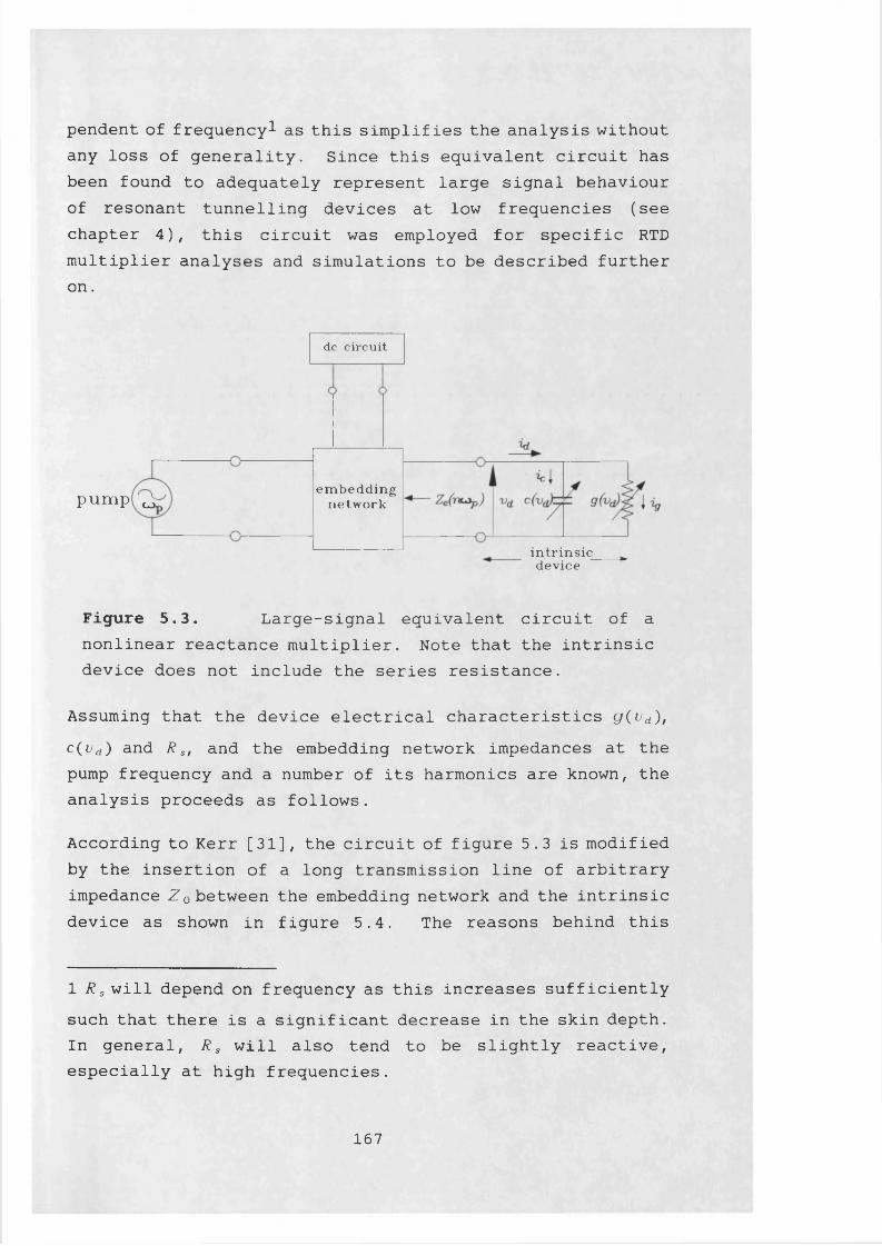
pendent of frequency! as this simplifies the analysis without any loss of generality. Since this equivalent circuit has been found to adequately represent large signal behaviour of resonant tunnelling devices at low frequencies (see chapter 4), this circuit was employed for specific RTD multiplier analyses and simulations to be described further on.
dc circuit
em beddingnetw orkP u m p ^
in tr in s icdevice
Figure 5.3. Large-signal equivalent circuit of anonlinear reactance multiplier. Note that the intrinsic device does not include the series resistance.
Assuming that the device electrical characteristics g ( v d),c(>d) and R s, and the embedding network impedances at the pump frequency and a number of its harmonics are known, the analysis proceeds as follows.
According to Kerr [31], the circuit of figure 5.3 is modified by the insertion of a long transmission line of arbitrary impedance Z 0 between the embedding network and the intrinsic device as shown in figure 5.4. The reasons behind this
1 R swill depend on frequency as this increases sufficientlysuch that there is a significant decrease in the skin depth. In general, R s will also tend to be slightly reactive, especially at high frequencies.
167
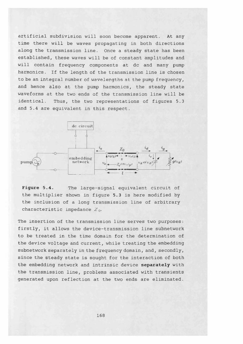
artificial subdivision will soon become apparent. At any time there will be waves propagating in both directions along the transmission line. Once a steady state has been established, these waves will be of constant amplitudes and will contain frequency components at dc and many pump harmonics. If the length of the transmission line is chosen to be an integral number of wavelengths at the pump frequency, and hence also at the pump harmonics, the steady state waveforms at the two ends of the transmission line will be identical. Thus, the two representations of figures 5.3 and 5.4 are equivalent in this respect.
dc c ir c u it
— I + V r(z)k ic
Z J n u J \yd c(vd>em bedd ing
n e tw o rk
Figure 5.4. The large-signal equivalent circuit ofthe multiplier shown in figure 5.3 is here modified by the inclusion of a long transmission line of arbitrary characteristic impedance Z Q.
The insertion of the transmission line serves two purposes: firstly, it allows the device-transmission line subnetwork to be treated in the time domain for the determination of the device voltage and current, while treating the embedding subnetwork separately in the frequency domain, and, secondly, since the steady state is sought for the interaction of both the embedding network and intrinsic device separately with the transmission line, problems associated with transients generated upon reflection at the two ends are eliminated.
168
Thus, the device waveforms are determined from figure 5.4 by alternately solving two much simpler circuits, each of which is in steady state with the transmission line.
The analysis starts by determining the voltage and current waveforms in the time domain. The time-dependent voltage and current are then transformed to the frequency domain, where the waveforms at the two ends of the transmission line are compared. If these are the same then the large signal problem has been solved; i.e. vd and id are respectively equal to va and ta in figure 5.4. If the terminal conditions are not satisfied, then a new waveform reflected off the embedding network is determined and the circuit analysis repeated. The solution converges when waveforms from the last reflection cycle match the ones from the previous cycle to within a specified accuracy.
5.3.2 Details of the large signal analysis
Referring to figure 5.4, at a general point along the line there will be a set of left- and right- travelling waves which are related to the total voltage {v) and current (i) at point by
v(z) = vr(z) + vl (z)
i(z) = ir(z)-il(z)
vr(z)-vi(z)Z 0
As the transmission line (of length I) is an integral number of wavelengths at all harmonics, the conditions that must prevail in steady state are:
v(0) = v(l) (5.7)
t(0) = i(l) (5.8)
(5.5)
(5.6)
169
Since a form of the harmonic balance technique will be used to assess the degree of convergence according to the conditions (5.7) and (5.8) in the frequency domain, vd and id must be expanded into Fourier series:
oo
vd W ~ I , V d>exp(;nu3pt) (5.9a)
+ 7 / 2
v d„ = f f ud(t)exp(-jn<x>pt)dt (5 .9 b)- 7 / 2
00
id ( 0 = l l d xp(JnM p 0 (510a)
+ 7 / 2
ld* = f f ‘“(Oexp(-jnMpt)dt (5.10b)- 7 / 2
where oop is the radian frequency of the pump. Using theFourier coefficients V dn and Id„of the intrinsic device voltage and current, the conditions (5.7) and (5.8) may be expressed in the frequency domain by
v d> (5.ii)— = Z,(n«) b')*Rs, n = 2 ,3,...<*>
V p- V d] (5.12)— --- 1 = Ze(Mp) + RsId,V dc- v d. (5.13)
I
where V p and V dc are the Thevenin equivalent pump and dc voltages, respectively, seen by the intrinsic device.
Now, assume that the transmission line in figure 5.4 is terminated by an impedance Z 0 until time t = 0 when the device is first connected to the circuit. At time t = 0 + a right
170
propagating wave will exist on the line, with Fourier components at dc and at the pump frequency. On the device side of the transmission line (z=l), these are
(5.14)
for the dc component and,
(5.15)
- V
at the pump frequency.
Figure 5.5a represents the nonlinear subnetwork consisting of the intrinsic device and the transmission line in the time domain, with V ro and V rj given by (5.14) and (5.15). The state equation for this circuit is
where us( 0 is the sum of the voltage sources across the
differential equation which can be solved numerically over a number of pump cycles, starting from an initial value of Vd(t = 0), if c(ud) and ig(ud) are known. This then gives the steady state voltage waveform ud ( 0 which will contain frequency components at all the pump harmonics. We now require the Fourier series coefficients of this new left-travelling wave. Solving (5.5) and (5.6) for vt(z) gives
(5.16)
transmission line. Equation (5.16) is a nonlinear
v(z)-i(z)Z o (5.17)2
171
such that at the device-end of the transmission line,
^d(Q-td(0 ^o2
(5.18)U|(0
Now, since the transmission line is an integer number of wavelengths at all the pump harmonics, equation (5.7) holds. Thus, the Fourier series coefficients of the left-traveling wave incident on the embedding network are given by
where V da and Idn are the Fourier series coefficients of t'dCOand id(0 taken over one pump cycle with period T = 2n/uop. The frequency domain analysis proceeds by calculating the reflected amplitude components at each pump harmonic from a knowledge of the reflection coefficient, fn, which is given
The wave reflected from the embedding network becomes the new right-travelling wave on the transmission line and its Fourier coefficients at all harmonic frequencies above the pump are
At dc and the pump frequency, the respective components are incremented by the dc and pump voltages:
Figure 5. 5b represents the additional voltage components produced by the device over the previous pump cycle as a string of voltage sources, the sum of which defines the new
V (5.19)A
by
Z e(n) + Rs-Z o Z «(rc) + R s + Z o
(5.20)
r.V,.. (n>l) (5.21)A
V (5.22)
V r,v, +v (5.23)
172
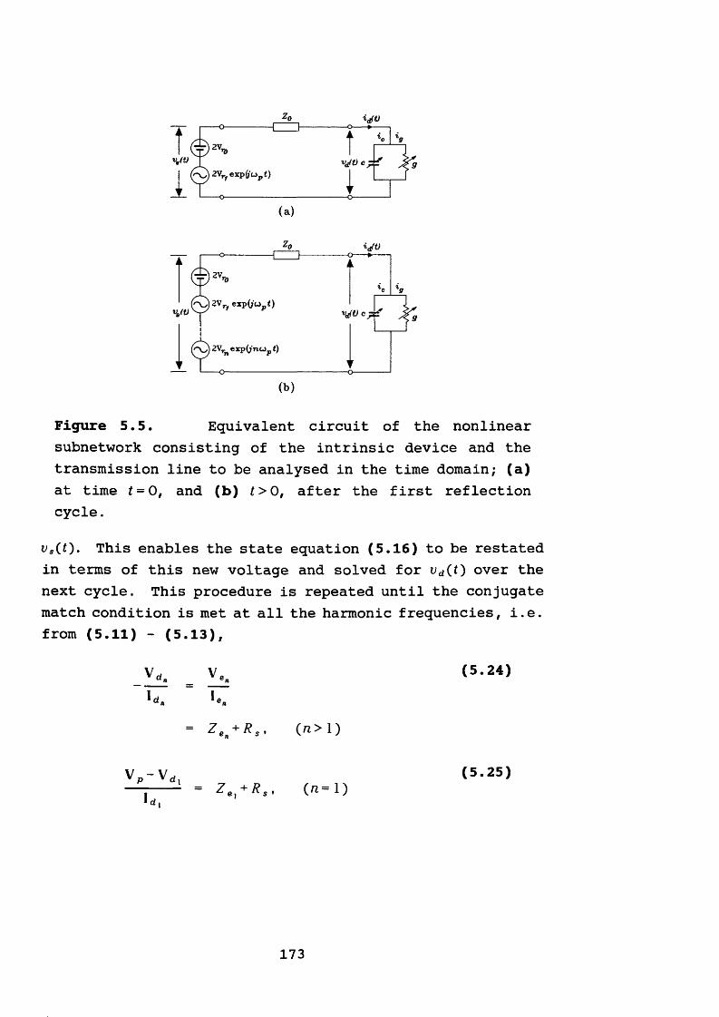
tV,(t)
>~sj) 2Vrfexp{3L>p t)
(a)
ijt)tVj/t) c
1
2V,
(b)
Figure 5.5. Equivalent circuit of the nonlinearsubnetwork consisting of the intrinsic device and the transmission line to be analysed in the time domain; (a) at time t = 0 , and (b) t > 0 , after the first reflection cycle.
vs(t). This enables the state equation (5.16) to be restated in terms of this new voltage and solved for vd(t) over the next cycle. This procedure is repeated until the conjugate match condition is met at all the harmonic frequencies, i.e. from (5.11) - (5.13),
Vd,id.
v,
- Z.+R,, (n> 1)
(5.24)
v„-vd- - Z + R , (n= 1)
(5.25)
173
5.4 The multiplier analysis program
The performance of a multiplier can be assessed by its conversion efficiency which is defined here as:
conversion efficiency _ o u t p u t p o w e r at n th h a r m o n i c (5.26)to n th h a r m o n i c p o w e r a b s o r b e d at p u m p f r e q u e n c y
This quantity depends upon the large signal waveforms at the diode and on the embedding impedance of the multiplier at the pump frequency and its harmonics. These intrinsic device voltage and current waveforms may be found using the multiple reflection technique described in section 5.3. The multiplier analysis program described here implements this technique to estimate the diode waveforms and the input and output impedances of the multiplier. This results in the calculation of conversion efficiency (or conversion loss^-).
The program is a modification of an original developed by Siegel, Kerr and Hwang [40]. Section 5.4.1 outlines the large signal calculation which is carried out in subroutine LGSIG which forms the main body of the program and is responsible for calculating the steady state diode waveforms - the most fundamental procedure in the whole analysis. The program listing given in Appendix V is one particular version used to simulate the performance of a RTD multiplier over a range of pump powers and bias voltages. Some of these results are discussed in section 5.5.
5.4.1 The large signal analysis subroutine
The multiplier program begins with a call to subroutine LGSIG to perform the large signal analysis using the multiple reflection technique. The embedding network impedances ZeH = Z e( nuop) from the pump frequency up to the highest
_ _ . _ _ _ , f power absorbed at pump input port "N ,1 Defined as lOlog ----------- r— jrr----: :— :— in° V, output power into the n harmonic port impedance/
174
harmonic considered (of order NH, assumed even) are formed in subroutine ZEMBED which is called by LGSIG. The real and imaginary parts of the embedding impedances are stored in arrays ZER ( - K ( Z 6n)) and ZEI ( = 3 ( Z 6ji) ) . The dc term is considered separately. The series resistance (RS)# which is here assumed purely resistive^, is added to each element of ZER and a complex array ZEMB(I) = ZER(I) + RS + ^ER(I), 1=1,...,NH is formed.
Following the calculation of the embedding impedances ZEMB and ZEMBDC (the dc embedding impedance), ZEMBDC is arbitrarily set equal to Z 0 (ZO), the characteristic impedance of the hypothetical transmission line. This has no effect on the final steady state solutions, as long as we adjust the dc Thevenin equivalent voltage source accordingly during the calculation of the actual bias voltage at the end of the large signal analysis. In fact, in the mixer program of Ref. [40], the embedding impedance at dc and the LO frequency are, at this stage, both equated to Z 0 as this modification speeds up the nonlinear analysis by reducing the number of constraints imposed on the device waveforms by the embedding network. In the case of a multiplier, however, the dc current is not generally known apriori.
At this point it is worthwhile digressing to describe how this problem is resolved in the subroutine CALBIAS which is called by LGSIG after the nonlinear analysis has been performed. With ZEMBDC set to Z 0, the dc bias voltage used in the program will be different from that which would actually be required to produce the calculated device rectified current (IDCOS(l)), unless the latter is negligibly small. Referring to figure 5.6a, which represents the dc equivalent circuit of the actual multiplier, the actual bias voltage can be written as
1 At high frequencies it would probably be necessary to include a reactive part with RS. This does not detract from the generality of the analysis.
175
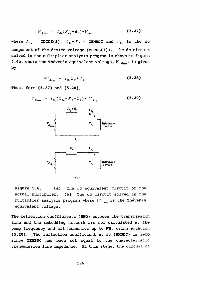
V , = Id (Ze + R S) + V t (5.27)
where /do = IDCOS(l), Z eo + R s = ZEMBDC and V do is the dccomponent of the device voltage (VDCOS(l)). The dc circuit solved in the multiplier analysis program is shown in figure 5.6b, where the Thevenin equivalent voltage, V'dhlaai is given by
Thus, form (5.27) and (5.28),
(5.28)
= Ii.(Z.+R.-Z0) + V (5.29)
(a)
1intrinsicdevice
(b)J
intrinsicdevice
Figure 5.6. (a) The dc equivalent circuit of theactual multiplier. (b) The dc circuit solved in the multiplier analysis program where V'dbtas is the Thevenin equivalent voltage.
The reflection coefficients (RHO) between the transmission line and the embedding network are now calculated at the pump frequency and all harmonics up to NH, using equation(5.20). The reflection coefficient at dc (RHODC) is zero since ZEMBDC has been set equal to the characteristic transmission line impedance. At this stage, the circuit of
176
figure 5.5a applies and the initial voltage wave (VR) on the transmission line propagating to the right towards the device is determined from equations (5.14) and (5.15). The multiple reflection algorithm is now initiated.
LGSIG calls the subroutine DRKGS, an IBM SSP integration routine implementing a Runge-Kutta algorithm with adaptive stepsize control, to solve the state equation (5.16) by determining ud(0 (Y(l)) in the time domain. The period of the voltage waveform is scaled so that one pump cycle occurs in 2n seconds. Subroutine FCT is called by DRKGS to set up (5.16) and evaluate dvd(t)/dt using the appropriate instantaneous value of the transmission line voltage sources vs(O (VS). The main modifications made to the program of Ref.[40] were in this particular subroutine. The original version evaluates the instantaneous values of ^(Ud)# c(ud) and g(ud) by calculation using analytical expressions for these quantities. In the present work, these values are obtained by interpolation from tabulated experimental data. It is assumed here that the device being analysed in the multiplier configuration has been adequately characterised at dc and microwave frequencies to obtain ig(ud) and c(i>d), as has been described in chapter 4, over a suitable bias voltage range and that an adequately effective small-signal equivalent circuit model of the device has been established over the frequency range of interest. The program should thus be capable of simulating the behaviour of particular devices in the desired multiplier configuration. The merits of this technique are discussed in section 5.5, where results of actual simulation runs are compared with experiment.
The routine DRKGS makes periodic calls to the subroutine OUTP at the appropriate stages of the integration to store the values of ud(0/ *d(O, ig(0/ ic(0# c(0 and g(0- Thus, at the end of one complete pump cycle, these quantities have been stored at equally spaced time intervals in their respective arrays, VDDATA, IDDATA, IGJDAT, ICJDAT, CJDATA
177
and GJDATA. The Fourier series coefficients of ud(0 and id( 0 over the pump cycle are then determined by a call to subroutine DFORIT. The coefficients V d and Id were defined
u i* u n
in equations (5.9) and (5.10) using the single ended exponential series representation. DFORIT uses the trigonometric series representation such that V d# = VDC0S(N+1) - yVDSIN(N+l) and ldn = IDCOS(N+l) - yIDSIN(N+l), where VDCOS(N+l) and IDC0S(N+1) are the cosine coefficients and VDSIN(N+1) and IDSIN(N+1) are the sine coefficients of the device voltage at harmonic N. This establishes the components of the left propagating wave on the transmission line (VL) and hence convergence according to equations (5.24) and(5.25) can now be tested by forming the ratios I V dj|/Id)( I / I (Z6(i + /?s) | (ZQMAG) at all harmonics up to NH. An integer flag, ZQFLAG, is augmented by 1 for every harmonic that does not give a value of unity to within the specified accuracy (ZQACC) for this ratio. If the value of ZQFLAG is non-zero, the right-propagating wave coefficients (VR) are calculated using equations (5.21) - (5.23). The time domain integration of the state equation (5.16) is repeated by calling DRKGS whence subroutine FCT would then use the new coefficients VR to determine the voltage sources vs and hence restate (5.16) on demand.
This procedure is repeated until the value of ZQFLAG is established as zero, i.e., conditions (5.24) and (5.25) are satisfied at all pump harmonics considered. LGSIG then calls subroutine MLTPER to calculate the multiplier performance as described in section 5.4.2 and the subsequent call to CALBIAS calculates the actual multiplier voltage required (VDCMLT) to give the calculated rectified current IDCOS(l) from (5.28).
178
5.4.2 Port impedances and conversion properties
The multiplier nonlinear analysis yields the device voltage, current, capacitance and conductance waveforms at a particular pump power level and dc bias. These waveforms can then be used to determine the input and output impedances and the conversion properties.
Figure 5.7 represents the equivalent circuit upon which is based the calculation of the multiplier conversion loss. The input impedance of the multiplier at any port is given
In the multiplier analysis program V dn and Idn are given by
The minus sign is required for the conversion from the trigonometric Fourier series representation generated by DFORIT into the complex form used elsewhere in the program.
The available pump power at port 1 is, from figure 5.7,
The program requires the value of V'lf the pump amplitude,and this is calculated in subroutine LGSIG as VLO from equation (5.33).
by
(5.30)
V d- = VDCOS(N +1) - y VDSIN(N +1) (5.31)
and
d IDCOS(N +1) - yIDSIN(N+1) (5.32)
(5.33)P1 a v a i l
179
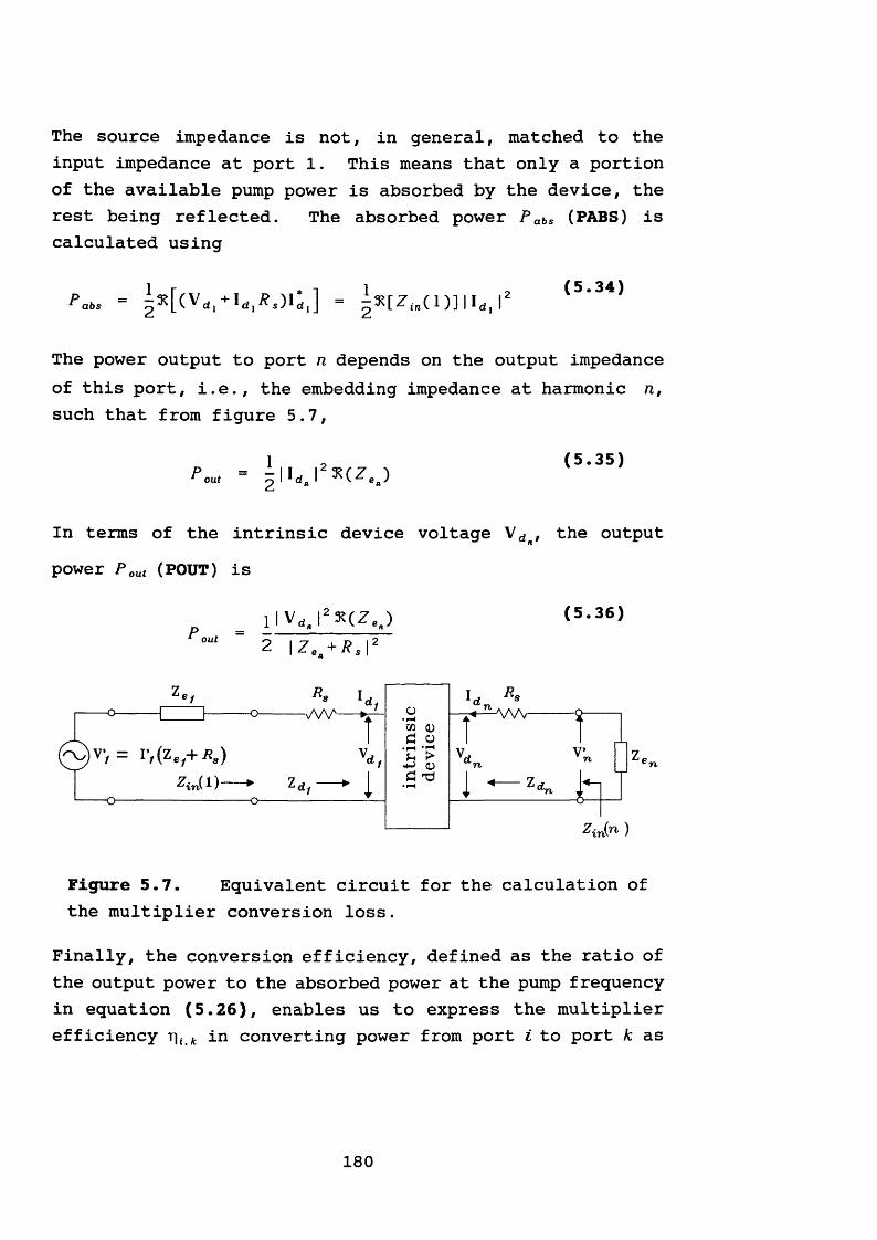
The source impedance is not, in general, matched to the input impedance at port 1. This means that only a portion of the available pump power is absorbed by the device, the rest being reflected. The absorbed power P abs (PABS) is calculated using
(5.34)
The power output to port n depends on the output impedance of this port, i.e., the embedding impedance at harmonic nt such that from figure 5.7,
out(5.35)
In terms of the intrinsic device voltage V d , the output power P out (POUT) is
outl l V d J ^ C f O 2 |Z.+/?S|2
(5.36)
0 vv=zin(D
03 <U
in(n )
Figure 5.7. Equivalent circuit for the calculation of the multiplier conversion loss.
Finally, the conversion efficiency, defined as the ratio of the output power to the absorbed power at the pump frequency in equation (5.26), enables us to express the multiplier efficiency r\i k in converting power from port i to port k as
180
Pou,(k) = H d J 2 ^[^.n(fc)] T1i‘ P a 6S ( 0 W ' t f n Z i ^ m
(5.37)
Normally one is interested in the conversion efficiency from the pump port to the nth harmonic port, in which case the conversion loss at port n is expressed as
The subroutine MLTPER is called at the end of the nonlinear analysis to perform the above calculations.
The definition of conversion efficiency (and consequently conversion loss) as stated in (5.37) is not strictly conventional. The object of the experiments and calculations described in section 5.5 was, however, to investigate the behaviour of a RTD when pumped with a microwave signal and not an attempt at designing and optimising a proper multiplier circuit. As such (5.37) expresses the conversion efficiency in a way which is effectively independent of the degree of mismatch at the input port.
In the case of a device, such as a RTD, exhibiting negative differential conductance, it is possible that the reflected power exceeds the incident. Hence, there might be gain at the fundamental frequency because the device acts as a reflection amplifier when biased in the NDC region. Thus, P abs will be negative and equations (5.37) and (5.38) will become ambiguous. For this reason, it was elected to resort to convention in such cases by substituting P abs by the incident power into a matched load in (5.37) and (5.38).
5.5 Experiment and analysis
This section describes a simple multiplier configuration used with the RTD 523B as the active device. It compares some of the experimental results obtained, mainly output
(5.38)LOSS(rc) -101og(Ti1>n)
181
power at the observed harmonics and rectified current as a function of bias voltage, with calculations performed using the computer program described in section 5.4 and listed in Appendix V. The device equivalent circuit model used was that derived in chapter 4 with the experimentally determined series resistance, differential conductance and capacitance.
5.5.1 Measurement of the harmonic output power
Figure 5 .8 shows the multiplier circuit and measurement set-up used to determine the power generated at a number of harmonics when the device is pumped at a set frequency and power level. The coaxial circuit is simple and its practical implementation facilitates accurate measurements of the embedding impedance seen by the device under test (DUT) at the pump frequency and its harmonics, thus enabling accurate determination of the available input and output power levels.
The microwave pump signal source used was a HP8350B sweep oscillator which was coupled to a 10 dB coupler (Triangle Microwave™ model CA-691) through an isolator (which transforms the source impedance to 50D). The pump signal then passes through the rf input port of the bias network (HP11612A) to reach the DUT, where some of the incident power is reflected and some absorbed. The device then generates harmonics because of the nonlinear nature of its I-V characteristic. These harmonics, along with the reflected part of the pump signal, then travel back along the input path through the coupler, which samples the output. The output power spectrum is then examined on the spectrum analyser (HP8593A) and the harmonic power levels measured. The dc circuit included a Time Electronics 9814 voltage calibrator in series with a Keithley 617 electrometer, both of which are programmable, thus enabling measurement of rectified current. In practice the measurement procedure was automated by using a pc with IEEE-488 interface capabilities as controller. This enabled a large number of
182
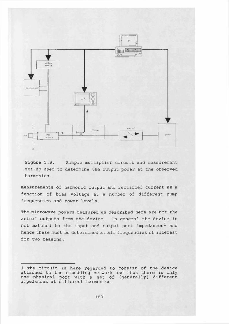
voltage
electrometer
S. A.
isolatorcoupler
biasnetwork
pumpDUT
Figure 5.8. Simple multiplier circuit and measurement set-up used to determine the output power at the observed harmonics.
measurements of harmonic output and rectified current as a function of bias voltage at a number of different pump frequencies and power levels.
The microwave powers measured as described here are not the actual outputs from the device. In general the device is not matched to the input and output port impedances 1 and hence these must be determined at all frequencies of interest for two reasons:
1 The circuit is here regarded to consist of the device attached to the embedding network and thus there is only- one physical port with a set of (generally) different impedances at different harmonics.
183
1 . to determine the coupling between the device package plane and the spectrum analyser input port, this will enable calculation of the actual power delivered by the device into the embedding network beyond the package,
2 . these impedances are required by the multiplier analysis program in order to perform the large- signal analysis and calculate the harmonic output power levels.
The coupling between the packaged device plane A (figure 5.8) and the spectrum analyser input port can be defined with reference to figure 5.9. Here the circuit between plane A, the coupler output port (2) and the spectrum analyser input port (3) is represented by a 3-port network. If a generator with source impedance equal to Z 0 is connected as shown to port 1 at reference plane A, then this sees the input impedance Z in at this port, which will not always be matched to Z 0. In fact, it can be observed from figure 5.10, which represents the VSWR at the packaged device plane A as measured with a HP8510B network analyser, that port 1 is not matched to 500 within certain frequency bands above about 6 GHz. This is to be expected since the design frequency band of the coupler was about 2 - 5 GHz.
Now, the incident power Pmc in figure 5.9 is the power whichwould be delivered to a matched load and this can be accurately measured at all frequencies of interest. Part of the incident signal is reflected giving rise to P r0f. A sample of the power absorbed in Z in will appear at port 3 to be measured by the spectrum analyser. This absorbed power, P in, is the required quantity and is thus given by
184
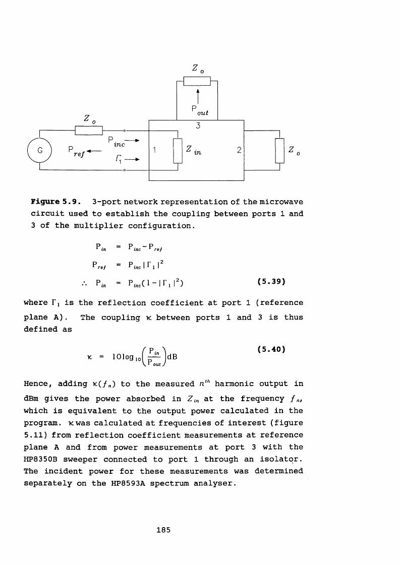
o
po u t
0 3
0
p.pref** 2 o
■o
Figure 5.9. 3-port network representation of the microwave circuit used to establish the coupling between ports 1 and 3 of the multiplier configuration.
where is the reflection coefficient at port 1 (referenceplane A ) . The coupling k between ports 1 and 3 is thus defined as
Hence, adding k (/„) to the measured nth harmonic output indBm gives the power absorbed in Z in at the frequency /„, which is equivalent to the output power calculated in the program, icwas calculated at frequencies of interest (figure 5.11) from reflection coefficient measurements at reference plane A and from power measurements at port 3 with the HP8350B sweeper connected to port 1 through an isolator. The incident power for these measurements was determined separately on the HP8593A spectrum analyser.
p = p - p1 in 1 inc x ref
?ref = PteclTj l 2
•*. Pte = PmcCi-irj2) (5.39)
(5.40)K
185
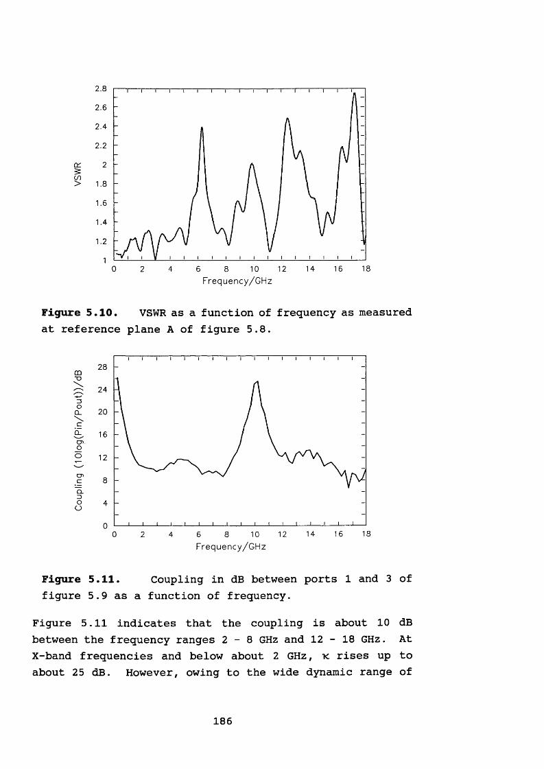
2.8
2.62.4
2.2
2
1.8
1.6
1.4
1.2
1180 12 166 10 142 4 8
Frequency/GHz
Figure 5.10. VSWR as a function of frequency as measured at reference plane A of figure 5.8.
28CDX I
24-t— 1
oQ_\ 20ch_cr>_oO
181612 140 2 6 8 104
Frequency/GHz
Figure 5.11. Coupling in dB between ports 1 and 3 of figure 5.9 as a function of frequency.
Figure 5.11 indicates that the coupling is about 10 dB between the frequency ranges 2 - 8 GHz and 12 - 18 GHz. At X-band frequencies and below about 2 GHz, k rises up to about 25 dB. However, owing to the wide dynamic range of
186
the spectrum analyser, useful measurements can still be made within these bands, since the coupling has been determined accurately.
5.5.2 Experimental results and simulation for a 1 GHz pump signal
5.5.2.1 Harmonic output power
The test set-up shown schematically in figure 5.8 was used to measure the output power at the first 8 harmonics1 at different pump frequencies and power levels as a function of bias voltage. At moderately high pump power levels (> 1 dBm) and/or bias voltages close to the NDC regions, higher harmonics right up to the highest measurable frequency were identified. Figure 5.12 shows a typical power spectrum of the RTD 523B pumped at 0.5 GHz at about 10 dBm, with the device at zero bias. The first line at 0.5 GHz represents the reflected signal. As can be expected, the odd harmonics are in general higher than the neighbouring even harmonics. This is due to the odd symmetry of the I-V characteristic.
For the purpose of simulation, the experimental results of chapter 4 were used to supply the multiplier program with the necessary data. Specifically, the device current and conductance, derived from the dc characteristic, and the capacitance c as well as dc/di>, obtained by numerical differentiation from the small-signal values of c, were tabulated in an input file together with all the other data elements required by the program. The voltages in the tabulation
1 The limitations imposed on frequency were partly due to the coaxial circuit and partly to the spectrum analyser. The measurement circuit included sma connectors which are specified up to 18 GHz, and the HP8593A maximum measurement frequency is 21 GHz.
187
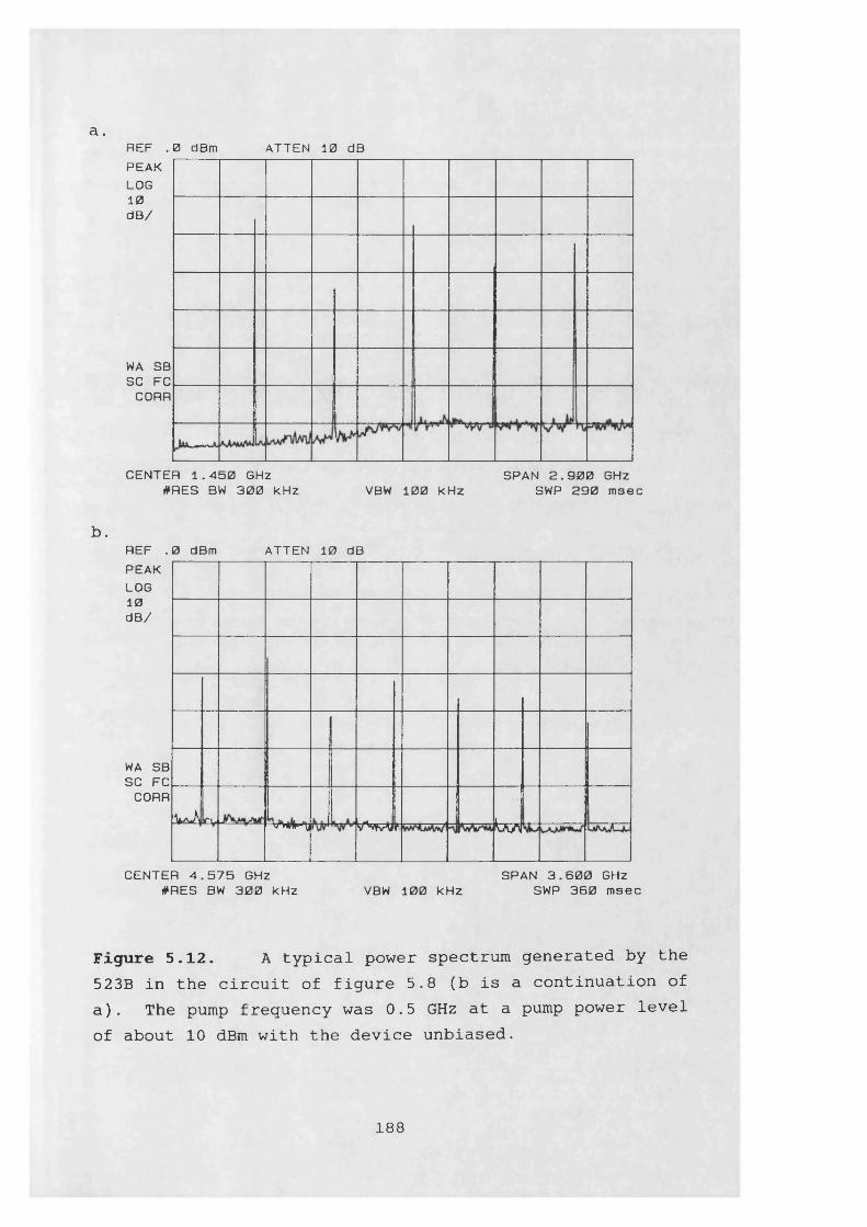
a .
REF .0 dBm ATTEN 10 dBPEAKLOG10dB/
WA SB SC FC CORR
CENTER 1.450 GHz SPAN 2.900 GHz#RES BW 300 kHz VBW 100 kHz SWP 290 msec
b.REF .0 dBm PEAK LOG 10 dB/
ATTEN 10 dB
WA SB SC FC CORR
V v \ r, i"v'rW'Hj VV v-W \A /\ |,
CENTER 4.575 GHz SPAN 3.600 GHz#RES BW 300 kHz VBW 100 kHz SWP 360 msec
Figure 5.12. A typical power spectrum generated by the 523B in the circuit of figure 5.8 (b is a continuation of a). The pump frequency was 0.5 GHz at a pump power level of about 10 dBm with the device unbiased.
188
were adjusted for series resistance using the same value derived in chapter 4, namely 4.40. Harmonics up to the eighth were considered in the analysis.
It was observed that with high power levels and/or high bias voltages, the time-domain integration of (5.16) demanded parameter values at voltages outside the measured range and as a consequence the convergence to the steady state solution could not be obtained. This was remedied by extrapolating the tabulated values as realistically as possible. For this purpose, the current beyond the tabulated points was assumed to increase in proportion to the square of the bias voltage, while the capacitance was assumed to approach zero exponentially. There is no experimental basis for these assumptions since the extrapolation was extended to ±50V 1 and therefore well outside the safe bias range of the device. The reason for such an apparently excessive extension of the tabulation range is that at certain instances during the derivative calculations, the integration algorithm might be required to calculate differences close to the machine precision. This might lead to instability. Clamping the voltage artificially to within the measured range did not prove to be effective at high bias voltages and/or pump power levels as either the analysis was inaccurate or convergence impossible. It was therefore hoped that by clamping the voltage to within the extended range would help to re-establish convergence more accurately. In fact, it was then found possible to obtain reasonably accurate simulations of multiplier performance at voltages right up to the extremes of the measured range and convergence was obtained in all the analyses performed.
1 The extent of this extrapolation might seem excessive. However a similar technique is often used which clamps calculated parameters during numerical integration to below limits which are far beyond the expected ranges. For example Siegel et al. [40] clamp the device voltage to below 100V in their mixer analysis.
189
Figure 5 .13a-g show the measured and calculated output powers at harmonics up to the 8 ^^ for a pump signal of 1.30 dBm (available power) at 1.00 GHz, with the I-V characteristic of the 523B superimposed on figures 5.13a and b. The agreement between experiment and calculation is good, at least up to the 5th harmonic. The simulated outputs diverge from measurement as higher bias voltages are reached. This may (at least partly) be due to inaccuracy in the extrapolated current, conductance and capacitance which was found necessary in order to artificially extend the range over which these values are input to the program. However, the calculated outputs still predict the same general trend of the measurements and mirror the slight divergence from odd-symmetry of the I-V and C-V characteristics. In particular refer to figure 5.13c and d. The point of inflection at about -0.3V occurring in the 4 ^ harmonic output is weaker than the corresponding one in forward bias. Although the calculated power in these regions is about 3 dB higher than the experimental value the same trend is evident. Similarly, the minimum power output at the 5*^ harmonic at about -0.3V is higher than that at 0.2V; the calculations predict this difference, although not accurately.
190
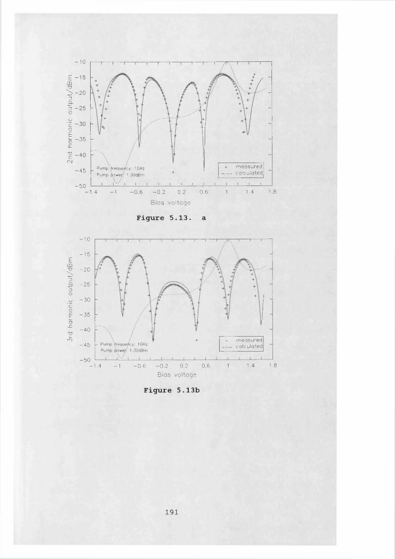
3rd
harmonic
output/dBm
2nd
harmonic
outp
ut/d
Bm- 1 0
-20
- 3 5
+ m easured calcula ted
Pump \frequericy: 1GHz Pump power; 1.30dBm
- 4 5
- 5 080.6 11.4 -1 - 0.6 - 0.2 0.2 1 . 4
Bias voltage
Figure 5.13. a
10
- 1 5
-20
- 2 5
- 3 0
- 3 5
- 4 0
+ measured calculated- Pump 'frequency: 1GHz
Pump ppwec; 1.30dBm- 4 5
- 5 01.80.6 1 . 4- 1 .4 - 0.6 - 0.2 0.2-1
Bias voltage
Figure 5.13b
191
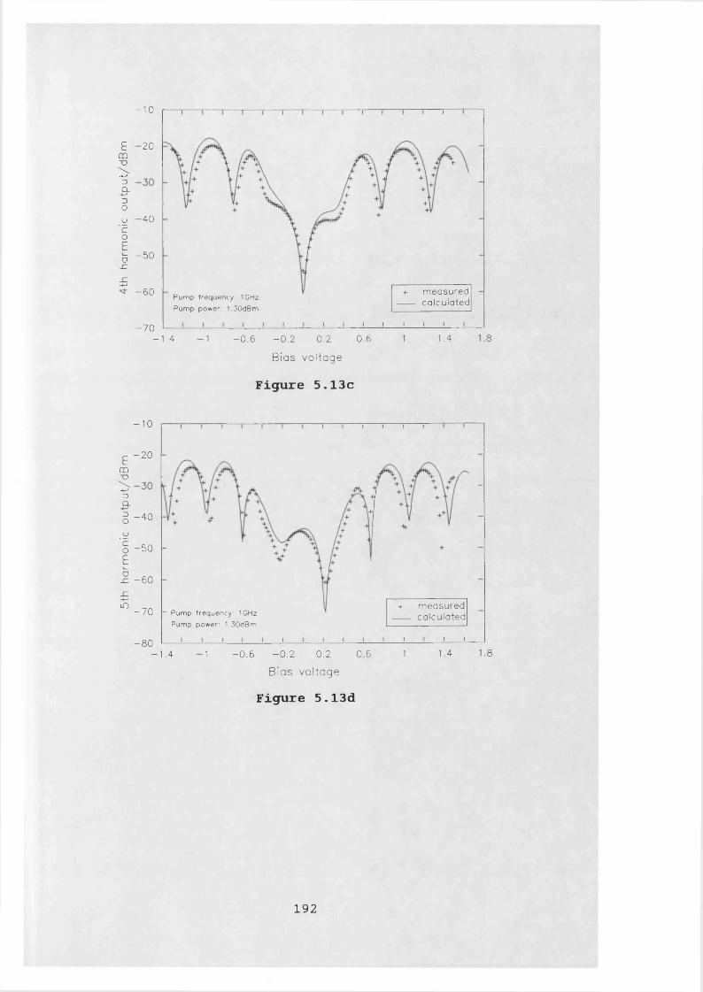
5th
harmonic
output/dBm
4th
harmonic
outp
ut/d
Bm- 1 0
-20
- 4 0
- 5 0
+ measured calcula ted
- 6 0 Pump frequency: 1GHz Pump power: 1.30dBm
- 7 080.6 1.4-1 .4 1 - 0.6 - 0.2 0.2
Bias voltage
Figure 5.13c
-10
-20
- 4 0
- 5 0
- 6 0
+ m easured calcu la ted- 7 0 ~ Pump frequency: 1GHz
Pump power: 1,30dBm
- 8 081.40.6 1- 1 .4 1 - 0.6 - 0.2 0.2
Bias voltage
Figure 5.13d
192
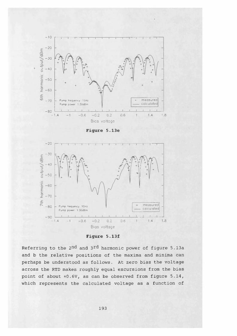
- 1 0
-20CD
- 3 0
C l
2 - 4 0
- 5 0
- 6 0
+ m easured calculated
Pump frequency: 1GHz Pump power: 1.30dBm
- 7 0
- 8 0- 0.6 - 0.2 0.6 1.8- 1 . 4 0.2 1.4
Bias voltage
Figure 5.13e
-20
- 3 0
*o- 4 0
a.
2 -50u
- 6 0
- 7 0
m easuredcalcu la ted
Pump frequency: 1GHz Pump power: 1.30dBm
- 8 0
- 9 08- 1 .4 0.6 1 1.4-1 - 0.6 - 0.2 0.2
Bias voltage
Figure 5.13f
Referring to the 2nd and 3rd harmonic power of figure 5.13a and b the relative positions of the maxima and minima can perhaps be understood as follows. At zero bias the voltage across the RTD makes roughly equal excursions from the bias point of about ±0.6V, as can be observed from figure 5.14, which represents the calculated voltage as a function of
193
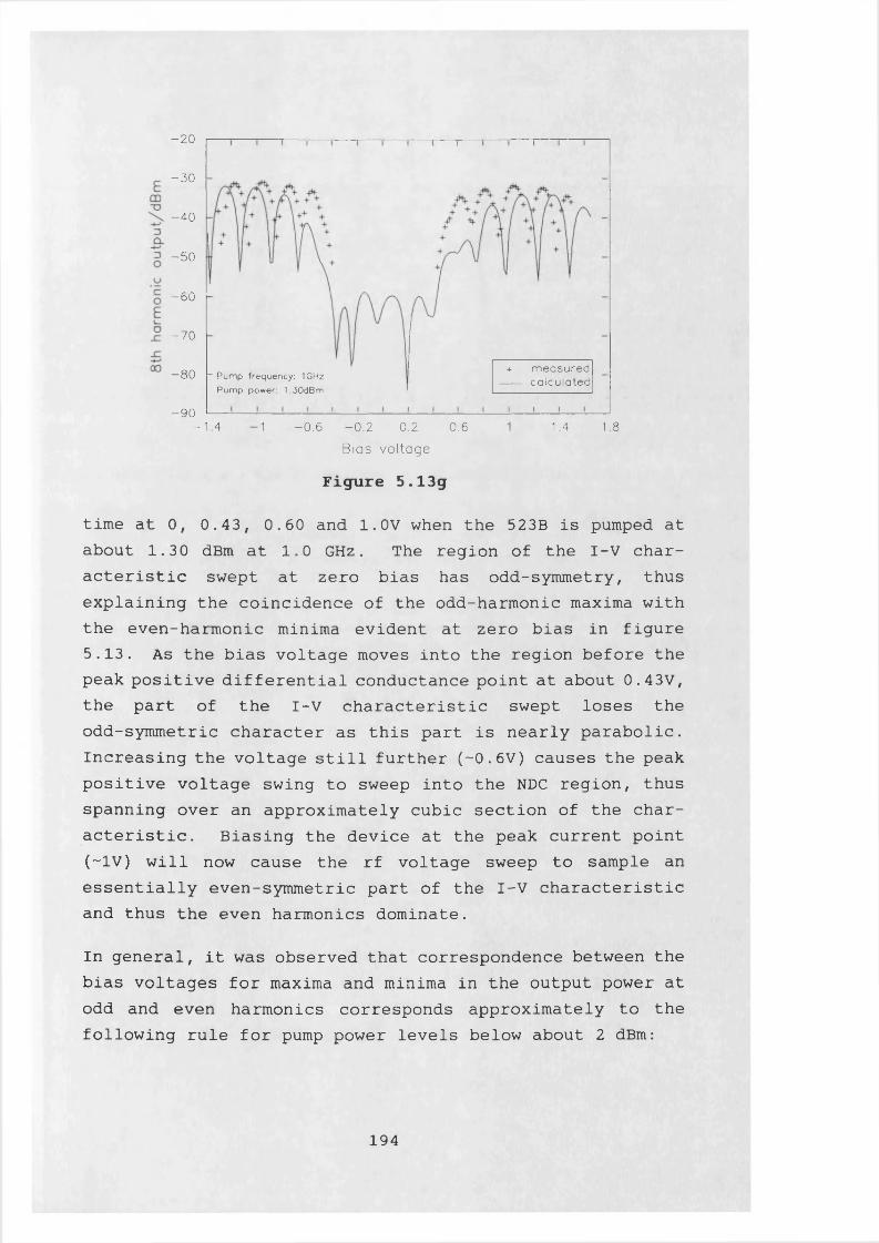
- 2 0
- 3 0
- 4 0
- 5 0
- 6 0
- 7 0
+ m easured calcu la ted- 8 0 “ Pump frequency: 1GHz
Pump power: 1,30dBm
- 9 0- 1 .4 1 - 0.6 - 0.2 0.2 0.6 1.81.4
Bias voltage
Figure 5.13g
time at 0, 0.43, 0.60 and 1.0V when the 523B is pumped at about 1.30 dBm at 1.0 GHz. The region of the I-V characteristic swept at zero bias has odd-symmetry, thus explaining the coincidence of the odd-harmonic maxima with the even-harmonic minima evident at zero bias in figure 5.13. As the bias voltage moves into the region before the peak positive differential conductance point at about 0.43V, the part of the I-V characteristic swept loses the odd-symmetric character as this part is nearly parabolic. Increasing the voltage still further (-0.6V) causes the peak positive voltage swing to sweep into the NDC region, thus spanning over an approximately cubic section of the characteristic. Biasing the device at the peak current point (~1V) will now cause the rf voltage sweep to sample an essentially even-symmetric part of the I-V characteristic and thus the even harmonics dominate.
In general, it was observed that correspondence between the bias voltages for maxima and minima in the output power at odd and even harmonics corresponds approximately to the following rule for pump power levels below about 2 dBm:
194
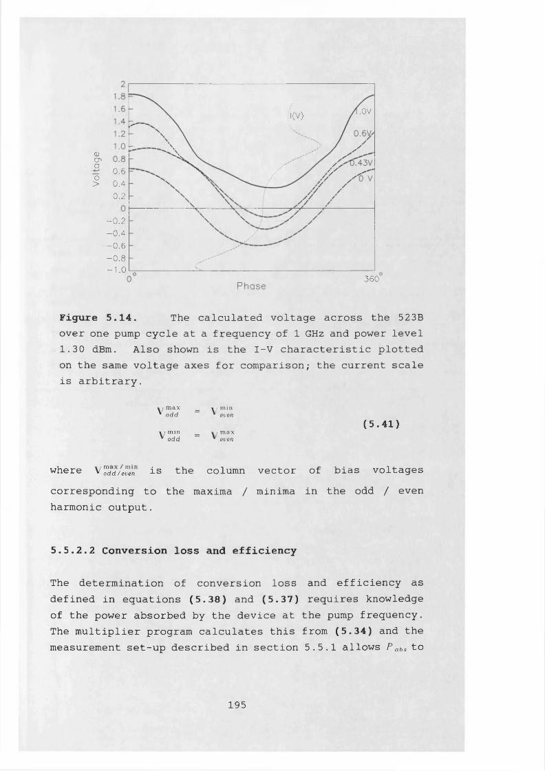
,0VI(V)
(Dcr>o 0.6 o> 0 .4
0.2 \\
-0.2- 0 . 4
- 0.6-0.8- 1.0
3 6 0
Figure 5.14. The calculated voltage across the 523Bover one pump cycle at a frequency of 1 GHz and power level 1.30 dBm. Also shown is the I-V characteristic plotted on the same voltage axes for comparison; the current scale is arbitrary.
V max _ « ; minodd ~ V even
(5.41)y min _ » r max
odd — * even
where V dd/e7en is the column vector of bias voltagescorresponding to the maxima / minima in the odd / even harmonic output.
5.5.2.2 Conversion loss and efficiency
The determination of conversion loss and efficiency as defined in equations (5.38) and (5.37) requires knowledge of the power absorbed by the device at the pump frequency. The multiplier program calculates this from (5.34) and the measurement set-up described in section 5.5.1 allows P abs to
195
be estimated from the reflected power at the pump frequency, which also appears on the spectrum analyser display (see figure 5.12) and was measured for this purpose. The measured value of the reflected power is appropriately scaled by the coupling k at the pump frequency as described in section 5.5.1 in order to determine the actual power reflected into port 1 of figure 5.9. The difference between the known incident power and the reflected power must then be the required power absorbed by the device.
Figure 5.15 shows the conversion loss to 2nc , 3rc*, 4t 1, 5t 1 and 6 th harmonics for a pump power level of 1.30 dBm at 1.0 GHz as a function of bias voltage. Again we see that the simulations predict the same general trends of the experimental results, with divergences between the two increasing with bias voltage. Figure 5.15 also shows that the maxima in conversion loss for odd harmonics coincide with the minima for the even harmonics and vice-versa as in the case of the output powers of figure 5.13.
196
Conversion
loss/dB
Conversion
loss
/dB
50harm onic 2
40
30
20
10
ump: 1.30dBm @ 1.0GHz
01.4- 1.4 -0.6 -0.2 0.2 0.6
Bias voltage
Figure 5.15. a
50harm onic 3
40
30
20
10
Pump: 1,30dBm @ 1GHz
01.40.2 0.6- 1.4 1 -0.6 -0.2
Bias voltage
Figure 5.15b
197
Conversion
loss/dB
Conversion
loss
/dB
60harm onic 4
50
40
30
20
Pump: 1.30dBm @ 1.0GHz
101.4- 0.6 - 0.2 0.2 0.6 1- 1 .4
Bias voltage
Figure 5.15c
70
harm onic 5
60
50
40
30
20Pump: 1.30dBm @ 1.0GHz
101.40.2 0.6- 1 .4 1 - 0.6 - 0.2
Bias voltage
Figure 5.15d
198
70harm onic 6
60
50(/)coococ/>
40
a>>coo
30
20Pum p: 1,30dBm © 1.0GHz
- 0.6 - 0.2 0.2 0.6- 1 . 4 1 1
Bias voltage
Figure 5.15e
Efficiencies of about 14% were measured for 2n( harmonic conversion with a pump power level of 1.30 dBm at 1 GHz at bias voltages corresponding to the minima of figure 5.15a and in excess of ±1.4V. For bias voltages within the NDC regions conversion efficiencies to the 3r< and 5*.h harmonics peaked to about 12% and 1.3%, respectively. The limit for purely resistive diode multipliers [13,14,15] would suggest11.1% and 4.0% conversion efficiency for these harmonics, thus, even with the unoptimised test set-up described in section 5.5.1, the harmonic conversion properties of the RTD seem promising. Table 5.1 gives the maximum observed and calculated conversion efficiencies over three different pump power levels; 1.30, 5.28 and 10.53 dBm at 1.0 GHz. The power at which these efficiencies were measured is the lowest used (1.30 dBm) and in this respect, the large-signal analysis predicts basically the same result except for the 7th harmonic, where the maximum efficiency was obtained at 10.53 dBm.
The maximum conversion efficiencies obtained experimentally are shown in figure 5.16 compared with calculated values for a pump signal frequency of 1 GHz at the 1.30, 5.28 and
199
Table 5.1: Maximum conversion efficiencies for 1.0 GHzpump signal
Harm.(No.)
Meas. Eff. %
PPL*(dBm)
Calc. Eff. %
PPL*(dBm)
2 14.9 1.30 8.41 1.303 11.5 1.30 5.93 1.304 3.02 1.30 3.21 1.305 1.30 1.30 1.53 1.306 0.637 1.30 0.752 1.307 0 . 2 2 0 1.30 0.255 10.538 0.276 1.30 0.157 1.30
*Pump power level 10.53 dBm power levels. Measured and calculated data show the same trend (except for the 7t 1 harmonic) in that at the lowest pump power levels, conversion efficiency is markedly higher. Now, refer to figure 5.17, which represents the calculated device voltage and current over one pump cycle at a bias voltage of 1.43V for the three pump power levels. Both the voltage and, even more so, the current show evidence of relatively smaller harmonic content at the higher power levels. This is due to the larger voltage swings obtained in the latter cases (e.g., about ±1.9V for the 10.53 dBm pump signal) which result in the device voltage being swept over a region of the I-V characteristic which is significantly wider than the highly nonlinear region between about 0 .9 and 1.4V during the pump cycle.
200
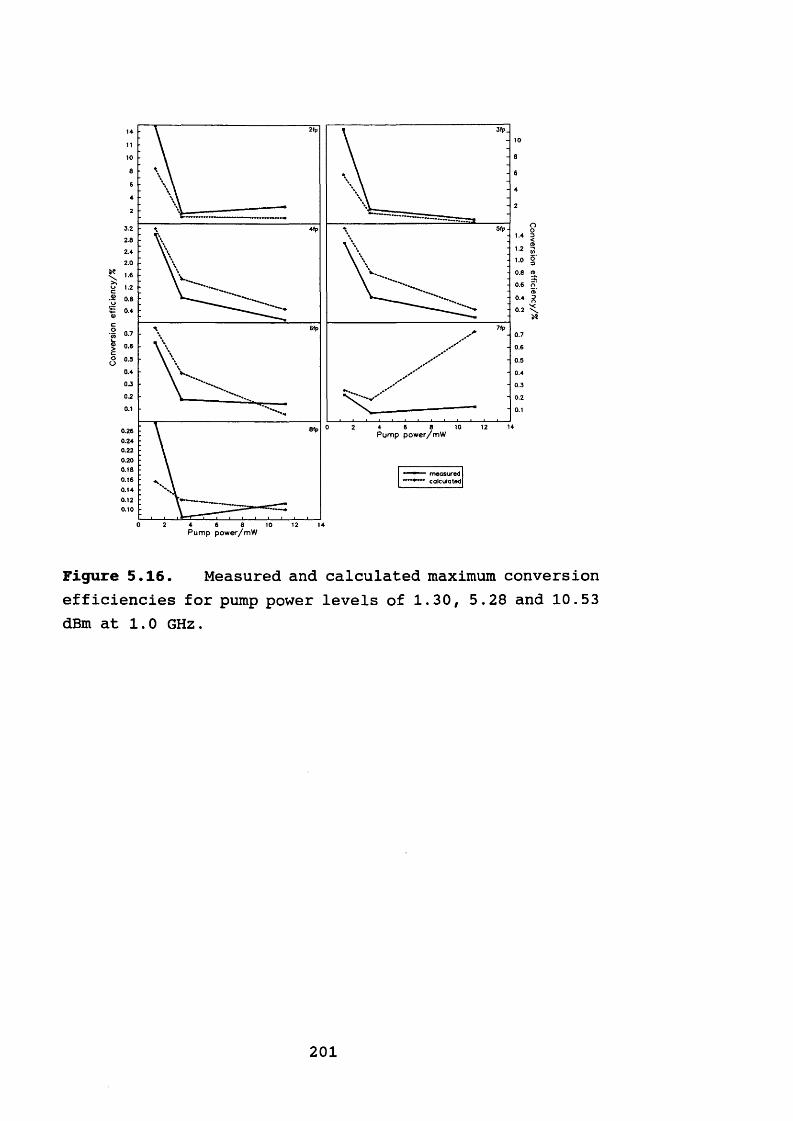
2fp1411
10
8642
3.2 5fp4fp2.8
2.42.0
1.2
0.80.4
7fp6fp0.7
0.40-3
0.1
8fp0.280.240.220.200.180.160.140.120.10
Pump power/mW
0 2 4 6 8 1210 14Pump power/mW
Figure 5.16. Measured and calculated maximum conversion efficiencies for pump power levels of 1.30, 5.28 and 10.53 dBm at 1.0 GHz.
201
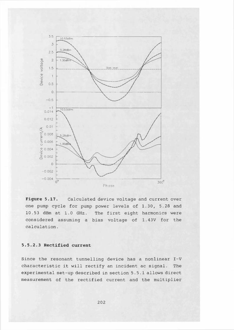
3.5 10.53dBm
5.28dBm2 . 5
1.30dBmCP x \Bias level
_0 . 5
- 0 . 5
10.53dBm0 . 0 1 4
0.012
0.01
c 0 . 0 0 8 5.28dBm
3 0 . 0 0 6
^ 0 . 0 0 4
" 0.002
- 0.002- 0 . 0 0 4
3 6 0Phase
Figure 5.17. Calculated device voltage and current over one pump cycle for pump power levels of 1.30, 5.28 and 10.53 dBm at 1.0 GHz. The first eight harmonics were considered assuming a bias voltage of 1.43V for the calculation.
5.5.2.3 Rectified current
Since the resonant tunnelling device has a nonlinear I-V characteristic it will rectify an incident ac signal. The experimental set-up described in section 5.5.1 allows direct measurement of the rectified current and the multiplier
202
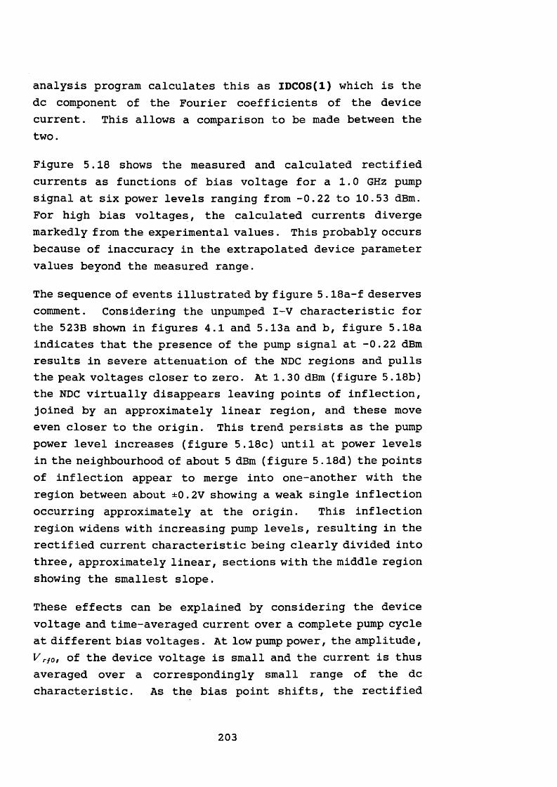
analysis program calculates this as IDCOS(l) which is the dc component of the Fourier coefficients of the device current. This allows a comparison to be made between the two.
Figure 5.18 shows the measured and calculated rectified currents as functions of bias voltage for a 1.0 GHz pump signal at six power levels ranging from -0.22 to 10.53 dBm. For high bias voltages, the calculated currents diverge markedly from the experimental values. This probably occurs because of inaccuracy in the extrapolated device parameter values beyond the measured range.
The sequence of events illustrated by figure 5.18a-f deserves comment. Considering the unpumped I-V characteristic for the 523B shown in figures 4.1 and 5.13a and b, figure 5.18a indicates that the presence of the pump signal at -0.22 dBm results in severe attenuation of the NDC regions and pulls the peak voltages closer to zero. At 1.30 dBm (figure 5.18b) the NDC virtually disappears leaving points of inflection, joined by an approximately linear region, and these move even closer to the origin. This trend persists as the pump power level increases (figure 5.18c) until at power levels in the neighbourhood of about 5 dBm (figure 5.18d) the points of inflection appear to merge into one-another with the region between about ±0.2V showing a weak single inflection occurring approximately at the origin. This inflection region widens with increasing pump levels, resulting in the rectified current characteristic being clearly divided into three, approximately linear, sections with the middle region showing the smallest slope.
These effects can be explained by considering the device voltage and time-averaged current over a complete pump cycle at different bias voltages. At low pump power, the amplitude, V rfo, of the device voltage is small and the current is thus averaged over a correspondingly small range of the dc characteristic. As the bias point shifts, the rectified
203
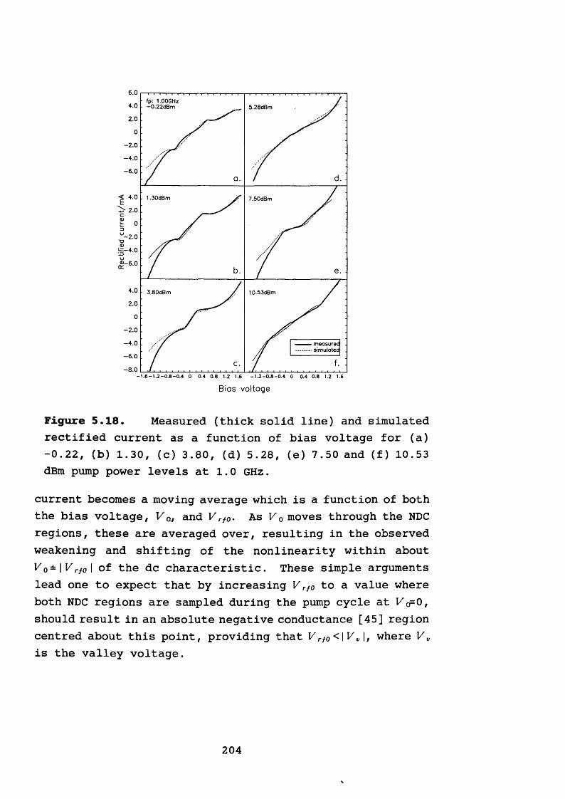
6.0fp: 1.00GHz -0.22dBm4.0 5.28dBm
2.0
- 2.0-4 .0
- 6.0
< 4.0 7 .5 0 d B m
> 2.0
- 2.0■4.0
e.
4.0 3.80dBm 10.53dBm
2.0
- 2.0-4 .0 - measured
simulated- 6.0- 8.0
1.6 - 1 . 2 - 0 . 8 - 0 .4 0 0 . * 0 .8 1.2 1.6 1 .2 - 0 .8 - 0 .4 0 0 .4 0 .8 1.2 1.6
Bias voltage
Figure 5.18, Measured (thick solid line) and simulated rectified current as a function of bias voltage for (a) -0.22, (b) 1.30, (c) 3.80, (d) 5.28, (e) 7.50 and (f) 10.53 dBm pump power levels at 1.0 GHz.
current becomes a moving average which is a function of both the bias voltage, V 0, and V rf0. As V 0 moves through the NDC regions, these are averaged over, resulting in the observed weakening and shifting of the nonlinearity within about Vo± \Vrfo \ of the dc characteristic. These simple arguments lead one to expect that by increasing K r/0 to a value where both NDC regions are sampled during the pump cycle at K(f0, should result in an absolute negative conductance [45] region centred about this point, providing that K r/0 < \V„\t where V v is the valley voltage.
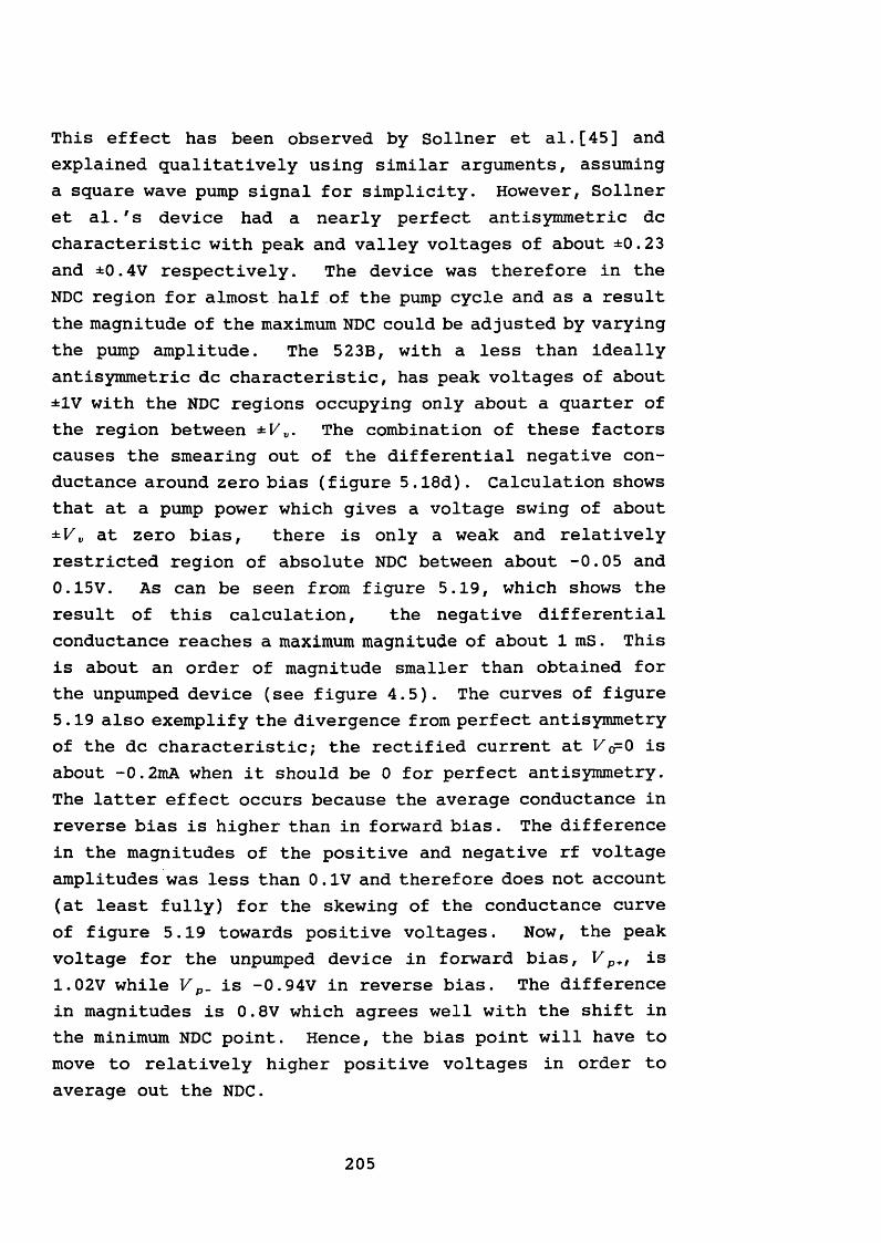
This effect has been observed by Sollner et al.[45] and explained qualitatively using similar arguments, assuming a square wave pump signal for simplicity. However, Sollner et al.'s device had a nearly perfect antisymmetric dc characteristic with peak and valley voltages of about ±0.23 and ±0.4V respectively. The device was therefore in the NDC region for almost half of the pump cycle and as a result the magnitude of the maximum NDC could be adjusted by varying the pump amplitude. The 523B, with a less than ideally antisymmetric dc characteristic, has peak voltages of about ±1V with the NDC regions occupying only about a quarter of the region between ±F„. The combination of these factors causes the smearing out of the differential negative conductance around zero bias (figure 5.18d). Calculation shows that at a pump power which gives a voltage swing of about ±K„ at zero bias, there is only a weak and relatively restricted region of absolute NDC between about -0.05 and0.15V. As can be seen from figure 5.19, which shows the result of this calculation, the negative differential conductance reaches a maximum magnitude of about 1 mS. This is about an order of magnitude smaller than obtained for the unpumped device (see figure 4.5). The curves of figure 5.19 also exemplify the divergence from perfect antisymmetry of the dc characteristic; the rectified current at Kq= 0 is about -0.2mA when it should be 0 for perfect antisymmetry. The latter effect occurs because the average conductance in reverse bias is higher than in forward bias. The difference in the magnitudes of the positive and negative rf voltage amplitudes was less than 0. IV and therefore does not account (at least fully) for the skewing of the conductance curve of figure 5.19 towards positive voltages. Now, the peak voltage for the unpumped device in forward bias, V p+, is 1.02V while K p_ is -0.94V in reverse bias. The difference in magnitudes is 0.8V which agrees well with the shift in the minimum NDC point. Hence, the bias point will have to move to relatively higher positive voltages in order to average out the NDC.
205
0.4
4.00.20.0
c -0.2
d - 0 .4
- 0.6- 0.8- 1.0
-1.01.2 6.35dBm 1 GHz
- 0 .5 -0 .3 -0.1 0.1 0.3 0.5
Bias voltage /V
Figure 5.19. Rectified current and conductance calculatedfor a 1.0 GHz pump signal at 6.35 dBm.
For pump amplitudes higher than V v, the occurrence of thelower slope central region in the characteristic can be understood as follows. As the bias starts increasing from zero, the portion of the I-V characteristic averaged over at first comprises both NDC regions, thus the net average conductance is reduced. As the bias shifts to higher, say- positive, voltages, a stage will be reached where the negative-going voltage swing reaches a point just before V p. and thus, the time averaged conductance over one pump cycle now increases since only the forward bias NDC region is encountered during the cycle. Similarly, for negative bias voltages the conductance increases as soon as the forward bias NDC region becomes inaccessible to the positive-going half-cycle. Thus the rectified cur- rent-voltage characteristic takes on the appearance of figure 5.18e.
206
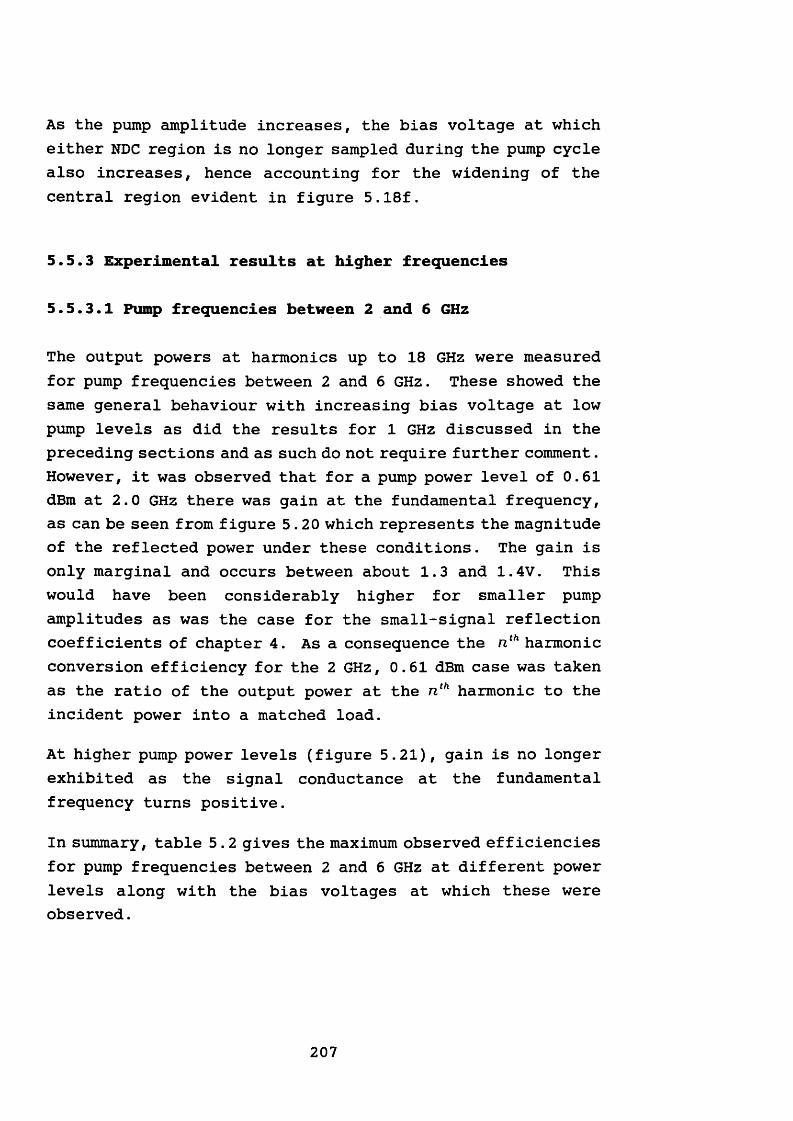
As the pump amplitude increases, the bias voltage at which either NDC region is no longer sampled during the pump cycle also increases, hence accounting for the widening of the central region evident in figure 5.18f.
5.5.3 Experimental results at higher frequencies
5.5.3.1 Pump frequencies between 2 and 6 GHz
The output powers at harmonics up to 18 GHz were measured for pump frequencies between 2 and 6 GHz. These showed the same general behaviour with increasing bias voltage at low pump levels as did the results for 1 GHz discussed in the preceding sections and as such do not require further comment. However, it was observed that for a pump power level of 0.61 dBm at 2.0 GHz there was gain at the fundamental frequency, as can be seen from figure 5.20 which represents the magnitude of the reflected power under these conditions. The gain is only marginal and occurs between about 1.3 and 1.4V. This would have been considerably higher for smaller pump amplitudes as was the case for the small-signal reflection coefficients of chapter 4. As a consequence the harmonic conversion efficiency for the 2 GHz, 0.61 dBm case was taken as the ratio of the output power at the n‘h harmonic to the incident power into a matched load.
At higher pump power levels (figure 5.21), gain is no longer exhibited as the signal conductance at the fundamental frequency turns positive.
In summary, table 5.2 gives the maximum observed efficiencies for pump frequencies between 2 and 6 GHz at different power levels along with the bias voltages at which these were observed.
207
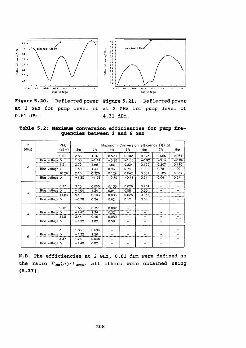
Refle
cted
po
wer
/mW pum p levs): 1.15mW
0.9
0.80.7
0.6
0.5
0.4
-1 .4 -0.61 -0.2 0.2 0.6 1 1 .4
Bias voltage
Figure 5.20. Ref lected power at 2 GHz for pump level of 0.61 dBm.
©5oCl
2.62.42.2'©
C£1.8
1.4
0.6 1.4- 0.6 - 0.2 0.2 111.4
Bias voltage
Figure 5.21. Reflected power at 2 GHz for pump level of 4.31 dBm.
Table 5.2: Maximum conversion efficiencies for pump fre quencies between 2 and 6 GHz
fp(GHz)
PP L(dBm) 2fp
M axim um Conversion e ffic iency (% ) a t 3fp 4fp 5fp 6fp 7fp 8fp
0.61 2.86 1.16 0.578 0.102 0.075 0.066 0.031Bias voltage > 1.50 -1 .1 4 -0 .9 0 -1 .0 8 -0 .9 2 -0 .8 2 -0 .8 6
4.31 2.75 1.96 1.65 0.224 0.155 0.207 0.110Bias voltage > 1.50 1.34 0.96 0.74 1.00 0.78 1.00
10.26 2.16 0.326 0.129 0.042 0.081 0.185 0.057Bias voltage > -1 .3 0 -1 .3 6 -0 .8 0 -0 .4 8 0.34 0.04 0.24
8.73 3.15 0.055 0.130 0.029 0.234 — -
Bias voltage > -1 .0 4 1.34 0.94 0.58 0.30 - -3 14.64 5.49 0.103 0.083 0.025 0.037 - -
Bias voltage > -0 .7 8 0.24 0.62 0.12 0.58 - -
9.12 1.65 0.351 0.092 _ — - -
4 Bias voltage > -1 .4 0 1.34 0.32 - - - -14.5 3.44 0.461 0.080 - - - -
Bias voltage > -1 .2 2 1.02 0.58 - - - -
3 1.83 0.694 _ _ _ - -
Bias voltage > -1 .3 2 1.26 - - - - -o8.37 1.28 0.548 - - - - -
Bias voltage > -1 .4 0 0.02 - - - - -
N.B. The efficiencies at 2 GHz, 0.61 dBm were defined as the ratio P out(n')/P avail, all others were obtained using (5.37).
208
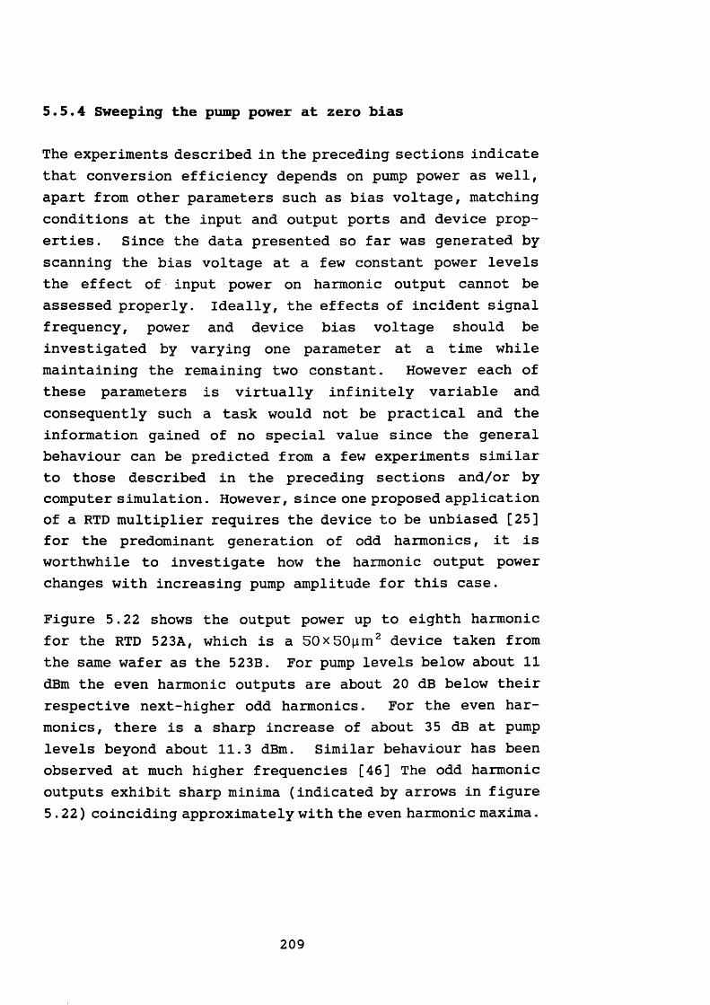
5.5.4 Sweeping the pump power at zero bias
The experiments described in the preceding sections indicate that conversion efficiency depends on pump power as well, apart from other parameters such as bias voltage, matching conditions at the input and output ports and device properties. Since the data presented so far was generated by scanning the bias voltage at a few constant power levels the effect of input power on harmonic output cannot be assessed properly. Ideally, the effects of incident signal frequency, power and device bias voltage should be investigated by varying one parameter at a time while maintaining the remaining two constant. However each of these parameters is virtually infinitely variable and consequently such a task would not be practical and the information gained of no special value since the general behaviour can be predicted from a few experiments similar to those described in the preceding sections and/or by computer simulation. However, since one proposed application of a RTD multiplier requires the device to be unbiased [25] for the predominant generation of odd harmonics, it is worthwhile to investigate how the harmonic output power changes with increasing pump amplitude for this case.
Figure 5.22 shows the output power up to eighth harmonic for the RTD 523A, which is a 5 0 x 5 0 n m 2 device taken from the same wafer as the 523B. For pump levels below about 11 dBm the even harmonic outputs are about 20 dB below their respective next-higher odd harmonics. For the even harmonics, there is a sharp increase of about 35 dB at pump levels beyond about 11.3 dBm. Similar behaviour has been observed at much higher frequencies [46] The odd harmonic outputs exhibit sharp minima (indicated by arrows in figure 5.22) coinciding approximately with the even harmonic maxima.
209
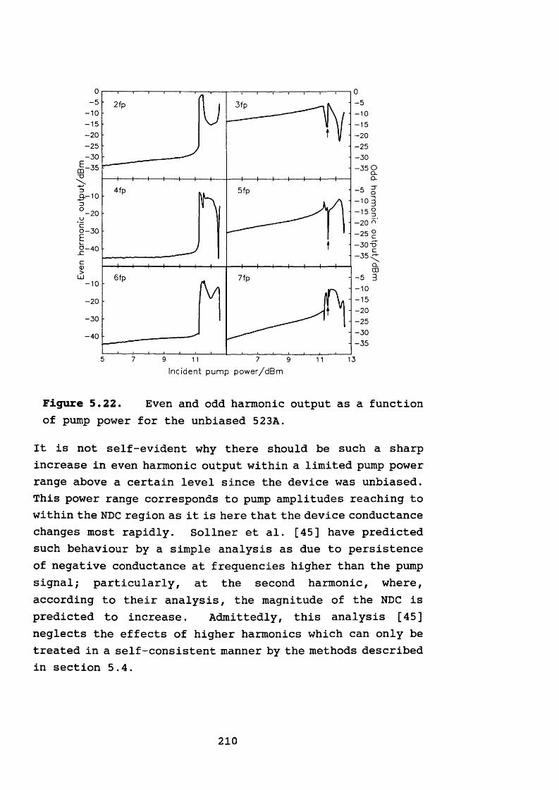
- 5-1 0-1 5-20-2 5-3 0
|-35T>
- 5- 1 0
-1 5-20-2 5-3 0-3 5 0
Cl Q-
2fp 3fp
4fp -5 E-1° 3- 1 5 °-20 °
-2 5 °- 3 0 -D c-3 5
Q.00
5fpQ .-1 0
-200 -3 0
6fp ?fpLJ-1 0
- - 1 0
- -1 5- -20- -2 5- -3 0- -3 5
-20-3 0
-4 0
5 7 9 7 1311 9 11
Inc ident pum p p o w e r/d B m
Figure 5.22. Even and odd harmonic output as a functionof pump power for the unbiased 523A.
It is not self-evident why there should be such a sharp increase in even harmonic output within a limited pump power range above a certain level since the device was unbiased. This power range corresponds to pump amplitudes reaching to within the NDC region as it is here that the device conductance changes most rapidly. Sollner et al. [45] have predicted such behaviour by a simple analysis as due to persistence of negative conductance at frequencies higher than the pump signal; particularly, at the second harmonic, where, according to their analysis, the magnitude of the NDC is predicted to increase. Admittedly, this analysis [45] neglects the effects of higher harmonics which can only be treated in a self-consistent manner by the methods described in section 5.4.
210
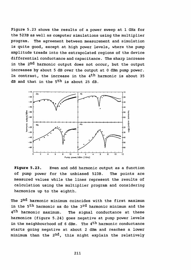
Figure 5.23 shows the results of a power sweep at 1 GHz for the 523B as well as computer simulations using the multiplier program. The agreement between measurement and simulation is quite good, except at high power levels, where the pump amplitude treads into the extrapolated regions of the device differential conductance and capacitance. The sharp increase in the 2 nc harmonic output does not occur, but the output increases by about 5 dB over the output at 0 dBm pump power. In contrast, the increase in the 4t 1 harmonic is about 35 dB and that in the 5 ^ is about 25 dB.
- 1 02 fp 3fp
-20
—30
-4 0
- 5 0
4 fp5fp-20
- 3 0
- 4 0 -
-5 0
- 6 0
0 2 6 8 124 10 6 8 100 2 4
Pump power/dBm (1GHz)
Figure 5.23. Even and odd harmonic output as a function of pump power for the unbiased 523B. The points are measured values while the lines represent the results of calculation using the multiplier program and considering harmonics up to the eighth.
The 2nc* harmonic minimum coincides with the first maximum in the 5t 1 harmonic as do the 3r( harmonic minimum and the 4 ^ harmonic maximum. The signal conductance at these harmonics (figure 5.24) goes negative at pump power levels in the neighbourhood of 6 dBm. The 4 ^ harmonic conductance starts going negative at about 2 dBm and reaches a lower minimum than the 2 n( , this might explain the relatively
211
higher conversion efficiency to the former at these power levels. One can also observe that the even harmonic conductance minima occur before the corresponding odd harmonic minima.
4.063.0
3.0
£ 0.8 2.00.6 2 ♦ 6 , 8 Pump power/dBm0.4
5fp 0.00.2 4fp
- 1.0
- 0.2- 2.0
- 0 .4- 3 .0
12100 82 6 64 8 10 2 4
Pump power/dBm
Figure 5.24. Signal conductance at the 2nc*, 3rc , 4"^ and 5tl1 harmonics calculated for the unbiased 523B as a function of pump power.
Finally, shown inset in figure 5.24 is the calculated signal conductance for the pump signal. The minimum corresponds in position with the others, but the interesting point is that the conductance remains positive throughout; thus signal amplification is not possible with the 523B at zero bias. However, the device still has potential as an unbiased multiplier.
5.6 Concluding remarks
A self-consistent method allowing large-signal analysis, the multiple reflection technique [31], has been discussed in detail. The multiplier program due to Siegel et al. [40] has been modified to take advantage of the small-signal characterisation of a RTD (the 523B; chapter 4) in such a
212
way as to allow actual experimental values of the device current and small-signal differential conductance and capacitance to be used during the analysis.
The same simple device equivalent circuit model of chapter 4 was used here and the program shown to simulate actual device behaviour in a simple multiplier configuration reasonably well. Thus, small-signal characterisation results can be used effectively in predicting the large- signal behaviour by the scheme outlined in the preceding sections.
The experimental set-up used did not allow any form of independent adjustment of the port impedances as it was kept as simple as possible in order to facilitate accurate measurement of embedding impedance at all harmonics of interest and thus be able to supply the necessary data for the computer simulations. However, the program could be used to home in on the optimum embedding impedances by iteration. For example if the required harmonic is the nth, then the bias voltage could be determined approximately by supplying arbitrary embedding impedances as a start. After the first run, the device nth harmonic impedance is noted and the n"' harmonic port matched accordingly, while terminating the other ports reactively. This procedure is then repeated until no further increase in the nth harmonic output is achieved. The embedding impedances thus obtained could serve as the design specifications for a potential multiplier.
The experimental results did not reveal conversion gain at any of the test bias voltages and pump power levels used. This was most likely due to two factors; device characteristics and unoptimised embedding impedances. Computer simulations performed using idealised I-V characteristics in order to investigate the factors effecting the conversion properties predicted the following:
213
1. For low pump power levels harmonic generation favours the second and to a lesser degree the fourth harmonic at bias voltages corresponding to the peak current points on the I-V curve. In this respect, a high peak-to-valley ratio (PVR) increases the low-order even harmonic outputs roughly in proportion to the product of the PVR and the peak current density.
2. For odd harmonic generation, the device should be unbiased and ideally have a perfect antisymmetric I-V characteristic. It should also have low values of V p, high PVR and peak current density but a NDC region which is wide relative to the pump amplitude so that the extremes of the voltage swings do not cross significantly into PDC regions where the signal conductance could revert to positive values.
Given these conditions and proper optimisation of the port impedances as described above, conversion gain is possible.
214
References1. R. Berenger, "The absorption of one-half centimetre electromagnetic waves in oxygen", Phys. Rev., Vol. 70, 1946, pp. 53-57.2. F. A. Benson and W. F. Winder, "Harmonic Generators and detectors for millimetre wavelengths", Proc. IEE, Vol. 115, 1968, pp. 37-42.3. N. R. Erickson, "A cryogenic receiver for 1mm wavelength", 6th Int. Conf. Infrared and Millimetre Waves: Conference Digest, 1981, pp. W-3-8.4. W. Gordy, "Millimetre and submillimetre waves in physics", in Millimetre Waves, Microwave Res. Inst. Symp. Series Vol. IX, Polytechnic Institute of Brooklyn, N.Y.: Polytechnic Press, 1959, pp. 1-23.5. C. M. Jhonson, D. M. Slager, and D. D. King, "Millimetre waves from harmonic gengenerators", Rev. Sci. Instr., Vol. 25, 1954, pp. 213-217.6 . W. C. King, "Millimetre wave spectroscopic components", IRE Trans. Microwave Theory Tech., Vol. MTT-2, 1954, pp. 13-16.7. A. Mardon, "Non-linear resistance and non-linear reactance devices for harmonic generation", in F. A. Benson (ed.), "Millimetre and Submillimetre Waves", Ilffe Books Ltd., London, 1969, pp. 179-191.8 . A. H. Nethercot Jr., "Harmonics at millimetre wavelengths", IRE Trans. Microwave Theory Tech., Vol. MTT-2, 1954, pp. 17-19.9. R. S. Ohl, P. P. Budenstein, and C. A. Burrus, "Improved diode for harmonic generation of millimetre and submillimetre waves", Rev. Sci. Instr., Vol. 30, 1959, pp. 765-774.10. J. M. Richardson and R. B. Riley, "Performance of three-millimeter harmonic generators and crystal detectors", IRE Trans. Microwave Theory Tech., Vol. MTT-5, 1957, pp. 131-135.11. C. Nguyen, "A 35% bandwidth Q-to-W band frequency doubler", Microwave J., Sept. 1987, pp. 232-235.12. J. W. Archer and M. T. Faber, "High-output single- and dual-diode, millimeter-wave frequency doublers", IEEE Trans. Microwave Theory Tech., Vol. MTT-33, 1985, pp. 533-538.13. C. H. Page, "Frequency conversion with positive nonlinear resistors", J. Nat. Bur. Stand., Vol. 56, 1956, pp. 179-182.14. C. H. Page, "Harmonic generation with ideal rectifiers", Proc. IRE, Vol. 46, 1956, pp. 1738-1741.15. P. Penfield Jr., "Frequency-Power Formulas", John Wiley & Sons, New York, 1960.
215
16. J. M. Manley and H. E. Rowe, "Some general properties of nonlinear elements - Part Is General energy relations", Proc. IRE, Vol. 44, 1956, pp. 904-916.17. K. Rauschenbach, C. A. Lee, and M. V. Schneider, "High-frequency efficient reflection multiplier", IEEE Trans. Microwave Theory Tech., Vol. MTT-39, 1991, pp. 575-579.18. B. C. DeLoach Jr., "Recent advances in solid state microwave generators", in "Advances in Microwaves", Vol. 2, Academic Press, New York, 1967, p. 58.19. J. C. Irvin and N. C. Vanderwal, "Schottky barrier devices", in H. A. Watson (ed.), "Microwave Semiconductors and Their Circuit Applications", McGraw Hill, New York, 1969, pp. 340-369.20. J. Monroe and E. Feldman, "Ka band klystron replacement", IEEE Trans. Microwave Theory Tech., Vol. MTT-12, 1964, p. 553.21. C. A. Burrus, "Millimeter-wave point-contact and junction diodes", Proc. IEEE, Vol. 54, 1966, pp. 575-587.22. J. W. Archer, "Millimetre wavelength frequency multipliers", IEEE Trans. Microwave Theory Tech., Vol. MTT-29, 1981, pp. 552-557.23. N. R. Erickson, "A high efficiency frequency tripler for 230 GHz", Proc. 12th European Microwave Conf., 1982, pp. 288-292.24. A. Anders, H. Gronqvist, and E. Kollberg, "Millimetre- and submillimeter-wave multipliers using quantum-barrier- varactor (QVB) diodes", IEEE Electron Dev. Lett., Vol. 11, 1990, pp. 373-375.25. T. C. L. G. Sollner, E. R. Brown, and W. D. Goodhue, "Microwave and millimeter-wave resonant tunneling diodes", in F. J. Leonberger, C. H. Lee, F. Capasso, and H. Morkog (ed.), "Picosecond Electronics and Optoelectronics II", Springer Series in Electronics and Photonics, Vol. 24, 1987,pp. 102-108.26. T. C. L. G. Sollner, E. R. Brown, C. D. Parker, and W. D. Goodhue, "High-frequency applications of resonant-tun- neling devices", in J. M. Chamberlain, L. Eaves, and J.-C. Portal, "Electronic properties of multilayers and low-dimensional structures", NATO ASI Series B, Vol. 231, Plenum , New York, 1990, pp. 283-296.27. T. C. L. G. Sollner, E. R. Brown, W. D. Goodhue, and C. A. Correa, "Harmonic multiplication using resonant tunneling", J. Appl. Phys., Vol. 64, 1988, pp. 4248-4250.28. P. D. Batelaan and M. A. Frerking, "A quantum well frequency multiplier with millimeterwave output", Proc. 4th Int. Conf. Infrared Physics, Zurich, 1988, pp. 527-529.
216
29. A. Rydberg and H. Groquist, "Quantum-well high-effi- ciency, millimeter-wave frequency multiplier", Electron. Lett., Vol. 25, 1989, pp. 348-349.30. R. Bouregba, D. Lippens, L. Palmateer, E. Borkenhoff, M. Bogey, J. L. Destombes, and A. Lecluse, "Frequency multiplication using resonant tunnelling diode with output at submillimetre wavelengths", Electron. Lett., Vol. 26, 1990, pp. 1804-1806.31. A. R. Kerr, "A technique for determining the localoscillator waveforms in a microwave mixer", IEEE Trans. Microwave Theory Tech., Vol. MTT-23, 1975, pp. 828-831.32. H. C. Torrey and C. A. Whitmer, "Crystal Rectifiers", MIT Radiation Laboratory Series, Vol. 15, McGraw Hill, New York, 1948.33. L. Becker and R. L. Ernst, "Non-linear-admittancemixers", RCA Review, Vol. 25, 1964, pp. 662-691.34. G. F. Edwards, "Frequency conversion by means of anon-linear admittance", Bell Systems Tech. J., Vol. 35,1956, pp. 1403-1416.35. A. C. MacPherson, "An analysis of the diode mixerconsisting of a non-linear capacitance and ohmic spreading resistance", IRE Trans. Micrwowave Theory Tech., Vol. MTT-5,1957, pp. 43-51.36. G. C. Messenger and C. T. McCoy, "Theory and operation of crystal diodes as mixers", Proc. IRE, Vol. 45, 1957, pp. 1269-1283.37. M. R. Barber, "Noise figure and conversion loss of the Schottky barrier mixer diode", IEEE Trans. Microwave Theory Tech., Vol. MTT-15, 1967, pp. 629-635.38. D. A. Fieri and L. D. Cohen, "Nonlinear analysis of the Schottky-barrier mixer diode", IEEE Trams. Microwave Theory Tech., Vol. MTT-21, 1973, pp. 39-43.39. W. K. Gwarek, "Nonlinear analysis of microwave mixers", M.S. Thesis, Mass. Institute of Tech., Cambridge, Mass., 1974.40. P. H. Siegel, A. R. Kerr, and W. Hwang, "Topics in the optimization of millimeter-wave mixers", NASA Technical Paper 2287, March 1984.41. S. Egami, "Nonlinear, linear analysis and computer aided design of resistive mixers", IEEE Trams. Microwave Theory Tech., Vol. MTT-22, 1974, pp. 270-275.42. M. Gupta and R. Lomax, "A self-consistent large signal analysis of a Read-type IMPATT diode oscillator", IEEE Trams. Electron Dev., Vol. ED-18, 1971, pp. 544-550.43. R. Hicks and P. J. Khan, "Numerical technique for determining pumped nonlinear device waveforms", Electron. Lett., Vol. 16, 1980, pp. 375-376.
217
44. R. Hicks and P. J. Khan, "Numerical analysis of nonlinear solid-state device excitation in microwave circuits", IEEE Trans. Microwave Theory Tech., Vol. MTT-30, 1982, pp. 251-259.45. T. C. L. G. Sollner, E. R. Brown, W. D. Goodhue, and H. Q. Le, "Microwave and millimetre-wave resonant tunneling devices", in F. Capasso (ed.), "Physics of Quantum electron devices", Springer Series in Electronics and Photonics, Vol. 28, 1990, pp. 147-180.46. R. Bouregba, D. Lippens, L. Palmateer, E. Borkenhoff, M. Bogey, J. L. Destombes, and A. Lecluse, "Frequency multiplication using resonant tunnelling diode with output at submillimetre wavelengths", Electron. Lett., Vol. 26, 1990, pp. 1804-1806.
218
CHAPTER 6
CONCLUDING NOTES
6.1 Introduction
Lack of time, funding and availability of devices suitable for high frequency operation were the main factors confining the experimental work discussed in this thesis to the lower microwave frequencies. However, some significant groundwork has yielded a number of useful results and indicated possible methods which may be employed in further investigation.
This final chapter discusses the main results presented and conclusions reached in the course of work which culminated in this thesis. The discussion on the various aspects of the microwave properties of resonant tunnelling devices and their small- and large-signal behaviour in different configurations indicates some of the areas for future investigation. The last section on techniques for improving the spectral purity and output power of RTD oscillators discusses some of the most recently reported novel ideas.
6.2 Summary and discussion of the main observations and conclusions
6.2.1 Bias circuit oscillations
The analysis of the device/bias-circuit interactions in chapter 2 indicates that experimentally observed behaviour can be well explained and predicted. Although it cannot be ruled out that some of the effects observed may be of
219
intrinsic origin, as yet there is no concrete evidence to support this view. This and similar works have shown the importance of device and circuit parameters in the analysis of extrinsic bistability. Indeed, it is possible to simulate the effects of extrinsic instability on I-V characteristics to the extent that qualitative agreement is achieved between the measured and calculated shape of the unstable NDC region and the extent of the hysteresis loops, and the dependence of these on circuit parameters, such as the series inductance, for a given device [1]. The lack of quantitative agreement is due to the over-simplified bias circuit assumed.
Consideration of stability criteria based on tunnel diode circuit analysis leads to two basic conditions for stability:
R sG d < 1 (6-l)
Q\L. (6 -2 )Cd <
where R s is the series resistance (circuit total), G d thedifferential conductance magnitude, Ls the circuit inductance and Cd the equivalent circuit capacitance.
The effects of maintaining stability in the bias circuit upon the output power of RTD oscillators have also been investigated. The requirements for high frequency power generation are found to be in conflict with those ensuring dc stability. The former demand a high peak current density and peak-to-valley ratio with a small device capacitance, while dc stability concerns lead to the inverse with the quantity = dominating. In fact, equation (2.27)shows a cubic dependence of the low-frequency stable rf power on AK. Thus, for stability, the maximum power calculated from stability considerations (equation (2.27)) must exceed the operating power output.
220
Now, in practice, the rf and dc circuits in a practical microwave oscillator are decoupled. This is usually achieved by biasing through a low-pass filter section. However, since the RTD exhibits negative conductance at all frequencies from dc to the oscillation frequency, the design of a bias circuit to suppress undesired oscillations over such a broad frequency range presents a formidable challenge. The solution to the problem may be to introduce lossy sections in the bias line rather than a low-loss reactive filter. This has been achieved for a 10 GHz RTD oscillator [2] by biasing through a parallel-plate transmission line constructed from fibreglass circuit board material. The high dielectric and metallic loss thus introduced lower significantly the Q of all resonances in the bias circuit. A conceptually similar arrangement is possible at millimetre and submillimetre-wave frequencies. In this instance, the RTD is typically contacted by a whisker inside a rectangular waveguide. The bias is supplied through a high-loss coaxial
A
ou tpu tbackshortRTD chipwhisker—
absorberdc bias pin
Figure 6.1. Schematic cross-section of a typical high frequency RTD oscillator used at the Lincoln Laboratory at M.I.T., showing the coaxial bias line with an iron-loaded high-loss section. (After Ref. [8])
221
line section, where the bias pin is effectively the centre conductor surrounded by iron-loaded epoxy [3,4,5,6 ,7,8 ], as shown in figure 6.1. The narrow gap between the top of the pin and the surrounding waveguide wall appears as a short circuit at high frequencies such that no rf power is lost down the bias line.
6.2.2 Small-* and large-signal equivalent circuits and some useful observations
An understanding of device behaviour in microwave circuits is dependent on an effective model which adequately represents the device physics whilst being simple and amenable enough to allow parameter extraction from microwave measurements. In this respect work at lower frequencies is advantageous as in this regime device physical properties, package and mount parasitics are relatively simple to model by lumped-element equivalent circuits. Furthermore, inaccurate parasitic element estimation will affect experimental results much more at higher frequencies. Another advantage of low frequency characterisation is that test and measurement systems are readily available up to frequencies of about 25 GHz where simple coaxial systems permit versatile and repeatable circuit realisation. Once an adequate understanding of the microwave properties of a device has been achieved and an accurate model derived, high frequency analysis of the model parameters should then follow. Together with feedback from theoretical studies, the analysis could then lead to fine-tuning the device model itself in order to allow high frequency device behaviour to be predicted.
The foregoing has been the motivation behind the work described in chapters 3 and 4. The LEW Techniques E10/A microwave package used for most of the microwave characterisation had not previously been characterised itself. This package offers an inexpensive and effective way of
222
mounting devices for reflection measurements in a 3.5 mm coaxial system. An accurate equivalent circuit model for the package in the specially-designed 3.5 mm coaxial mount described in chapter 3 has been derived for the frequency range 45 MHz to 13 GHz. This model was used with success in de-embedding the device impedance of a 20x20pim2 RTD bonded into an E10/A package mounted in a coaxial system.
Applying the equivalent circuit of a tunnel diode and fitting frequency independent parameters to the experimental data led to excellent agreement between measurement and simulation based on the extracted parameters. In particular, it was shown that the differential conductance obtained from dc characterisation can be used directly in the model. This allowed the determination of device capacitance over a wide range of bias voltages. For the first time it was found possible to fit a single-valued capacitance over the test frequency range of 45 MHz to 13 GHz, dependent only on bias voltage, as also was the case for the differential conductance. The small-signal equivalent circuit model thus constructed allows impedance estimates to within a difference of less than 5% of measurement.
This accuracy is thought to be due primarily to the accurate de-embedding procedures used. However other factors have influenced the results. In contrast to most published reports on microwave characterisation of RTD's employing basically the same technique of reflection measurements with a network analyser[9,10,11,12,13,13,14,15,16], the methods of parameter extraction used in the small-signal study did not make use of commercial CAD curve-fitting software. This type of analysis can result in a number of different equivalent circuit configurations which are all equally capable of generating a simulated frequency-response close to experimental observation. The lumped circuit elements thus extracted are, however, not always identifiable with the device physical properties. This is especially so in
223
cases where de-embedding is not accurate enough or part of the equivalent circuit representing the embedding network, such as the bonding wire inductance, is not determined beforehand thus leading to extra degrees of freedom for the fit. This type of analysis inevitably leads to attributing properties to the device which essentially pertain to the embedding network.
Another factor effecting the accuracy of small-signal characterisation is the test signal power used in the reflection measurements. An assessment has been made of this effect by repeating the measurements using a -10 dBm signal level instead of the original -20 dBm. This has led to the conclusion that at bias voltages corresponding to regions of relatively high nonlinearity in the I-V and C-V characteristics the equivalent circuit parameters exhibit frequency dependence. This is caused by the frequency-sensitive averaging effect of the pump signal through the varying degree of match between the device and the source. Since the device impedance is a function of frequency and is independent of the source impedance as seen through the embedding network, the degree of matching between the two is also a function of frequency. This means that the voltage amplitude across the device varies with frequency. Since at higher signal levels the voltage spans across an appreciable part of the I-V and C-V characteristics during the pump cycle, the differential conductance and capacitance will not be similar to the small-signal case and will, in turn, become frequency-dependent since they are effectively time-averaged values. The large-signal behaviour of a device can therefore become very complicated as the voltage amplitude across the device is self-consistently determined along with the impedance as stated here. Direct reflection measurements on the device using high test signal levels will therefore not reveal the true large-signal behaviour.
224
The solution is to allow the device to oscillate and attempt to adjust the output frequency independently of the power. In so doing, the steady-state condition for an oscillator, that is
Ztf(co) + ZI(u>) = 0 (6.3)allows the device impedance Z d to be determined frommeasurements of the load impedance Z L which the device sees at the oscillation frequency. This method restricts the frequency range and is difficult in practice since tuning the circuit for the required frequency will in general alter the output power. In the case of the large-signal impedance measurements of chapter 4, the coaxial double-stub tuner used could be adjusted to give the desired frequency and power (within the respective allowable ranges) by iteratively sliding the stub assembly and moving either or both stubs. Adjustment of the stubs resulted in significant change in the output power accompanied by a slight frequency shift, and vice-versa for changes in the position of the stub-assembly.
Large-signal impedance measurements thus performed revealed that within a narrow frequency range, the experimental data fitted the tunnel diode equivalent circuit model reasonably well. The fit was obtained with the same value of series resistance and roughly time-averaged values of the capacitance and negative conductance as in the small-signal case at the corresponding bias voltage.
In the course of the large-signal experiments it was observed that when the tuner adjustments were such as to permit the generation of narrow bandwidth, essentially single-frequency oscillations, bias circuit oscillations ceased to exist. This implies that when the RTD locks onto a cavity mode with a sufficiently high loaded Q the restrictions placed on the
225
bias circuit by stability considerations are relaxed. Hence, it would appear that the design of RTD oscillators has to be based on the realisation of high-Q cavities.
Another possible course of action could be the use of injection locking techniques. Although injection locking of RTD oscillators was not properly investigated in the present work, it was observed that the quality of the output spectrum can be improved markedly when a spectrally pure signal of low intensity is incident on the device. In brief, the packaged RTD is mounted in a coaxial circuit similar to the one used for the large-signal impedance measurements described in chapter 4, but modified as shown in figure 6.2 for this particular case. The device is biased in its NDC region and the tuner adjusted so that nearly single frequency microwave oscillations are observed, at which point the bias circuit oscillations desist. The oscillation frequency is then noted and the tuner stubs retracted to the point where the spectral quality is degraded and bias circuit oscillations reappear. The sweep oscillator is then used to provide an injection signal, typically at about -5 dBm, at a frequency close to (within about ± 20 MHz) the observed oscillation frequency of the RTD. At this point the spectrum consists of the fundamental at the injected signal frequency and its harmonics since the RTD is now acting as a harmonic multiplier. Providing that the circuit is not extensively de-tuned prior to the injection signal, the bias instabilities subside. The most interesting effect observed in this experiment is that when the injection signal is switched off, the RTD oscillation spectrum reverts to nearly its original form before the de-tuning took place. Thus it would seem that the device stays locked onto a cavity mode even in the absence of the injection signal, notwithstanding the degraded Q of the circuit. It was, however, observed that this situation was not indefinitely stable since the spectrum was observed to revert to its de-tuned form
226
immediately before the application of the injection signal. This occurred quite randomly and might have been caused by voltage transients in the bias line.
spectrum analyser
bias TeeDUT
coup ler in jec tion signadoub le—stub
tuner
dc c irc u it
Figure 6.2. Experimental set-up for the observation of the effects of an injection signal on the output spectrum of an RTD oscillator.
Injection locking of RTD oscillators has been almost overlooked in the literature. Due to its promise of improved output characteristics which could lead to practical applications, this aspect is worthy of further investigation.
6.2.3 Large-signal analysis and harmonic multiplication
The preceding section outlines the difficulties encountered in attempting to predict the large-signal microwave characteristic properties of essentially any nonlinear device, but in particular a device, such as the RTD, which exhibits a negative real part of impedance over a broad frequency range. When a rf signal is incident on a device with a nonlinear I-V and/or C-V characteristic the device voltage
227
and current waveforms have to be calculated in a self-consistent manner, where the interaction of the device and its embedding circuit are duly considered at the pump frequency and its harmonics. The type of harmonic balance technique applied in chapter 5 is a powerful tool which allows such a nonlinear analysis to be performed. It requires the assumption of a device equivalent circuit model and knowledge of the embedding impedance seen by the device in the test circuit at the pump frequency and a number of harmonics.
A nonlinear analysis program [17] that uses the multiple reflection technique [18], a form of the harmonic balance technique, was modified in such a way as to allow direct use of the experimentally-determined I-V (and G-V) and C-V characteristics, assuming the simple tunnel diode model. The circuit elements of this model were assumed frequency-independent and were determined from small-signal reflection measurements as described in chapter 4. A simple microwave circuit which allows measurement of harmonic output powers was used to provide means for direct comparison of calculated and measured harmonic output and conversion efficiency. The resulting agreement was encouraging and showed that the small-signal equivalent circuit model with the measured G(V) and C(K) can be used as the basis for predicting large-signal device behaviour.
The harmonic conversion properties of a RTD were examined as a function of bias voltage and pump power without attempting to optimise the embedding impedance of the experimental circuit. The results indicate that at bias voltages such that the rf voltage amplitude spans over a region of the I-V characteristic which is approximately antisymmetric, the odd harmonics dominate. Conversely, the even harmonics dominate when the rf voltage covers regions of approximate symmetry about the bias point. Hence, the potential exists for the use of RTD's as multipliers of not
228
just odd but also even harmonic output depending on signal power and bias voltage. To date the accent has been on odd (particularly 5th) harmonic multiplication[19,20,21,22,23], but the possibilities of efficient even (particularly 2 nc*) harmonic generation with low-level pump signals, when the device is biased at the peak voltage, cannot be overlooked.
Comparative studies using the same DBRTD heterostructure [24] as a quintupler and fundamental oscillator have revealed that the multiplier power drops more slowly than that of the oscillator with increasing output frequency, since multiplication still occurs beyond the oscillation cutoff frequency. Another advantage of amillimetre/submillimetre-wave multiplier is that locking the pump input signal at a relatively low frequency is easier than locking the fundamental oscillator at some five times that frequency. This suggests that the multiplier may be a better source of power in the submillimetre spectrum than a RTD fundamental oscillator.
The nonlinear analysis of chapter 5 allows the calculation of device rectified current and the experimental circuit permits its direct measurement. These were compared for a range of bias voltages at a number of different pump power levels. The experimental results are in good agreement with the simulations and allow qualitative interpretation of the decreasing nonlinearities of the rectified current-voltage characteristic with increasing signal power. In particular, there will be a certain power level which results in an absolute negative differential conductance region centred about zero bias. This mode of operation may prove useful as will now be briefly outlined.
Sollner et al. [25] have predicted that if an unbiased RTD is pumped at a frequency uo0/ say, a low-level signal at a frequency c jo s » c j o 0 can be amplified making use of the absolute
229
negative conductance. Furthermore, the magnitude of the negative conductance can be controlled by the pump amplitude, a very useful circuit property.
The predictions of Sollner et al. [25] were based on a very simple analysis which neglects the effects of pump harmonics higher than the second. A more accurate analysis performed with the modified multiplier program is described in chapter 5, and the results are shown in figure 5.24. This figure shows clearly that even though the conductance at the pump frequency is positive, the harmonics show regions of negative signal conductance within a range of pump power. The device is thus capable of amplifying signals at frequencies much higher than the pump. Now, if a resonant cavity is provided for the pump signal, the cavity Q controls the fraction of the pump signal energy stored per cycle. If Q is such that Qcd0 >cjus, oscillation at uos can be maintained in the absence of the original signal. Operation at zero dc bias implies that no dc connection need be made to the sample. Hence, the problem of dc stabilisation disappears since the dc circuit in which undesirable oscillations could occur is eliminated. *
Finally, the optimisation of device electrical characteristics for frequency multiplication was investigated using the multiplier analysis. The results indicate that for small pump signals with the device biased at the peak voltage, low-order harmonic generation is enhanced by higher peak-to-valley ratios. For predominant odd-harmonic generation, the device I-V characteristic should be as perfectly antisymmetric as possible and should be unbiased. Conversion efficiency in this case will be improved if the peak voltages in forward and reverse bias are low and the respective NDC regions wide relative to the pump amplitude so that the rf voltage does not cross significantly into the PDC regions
230
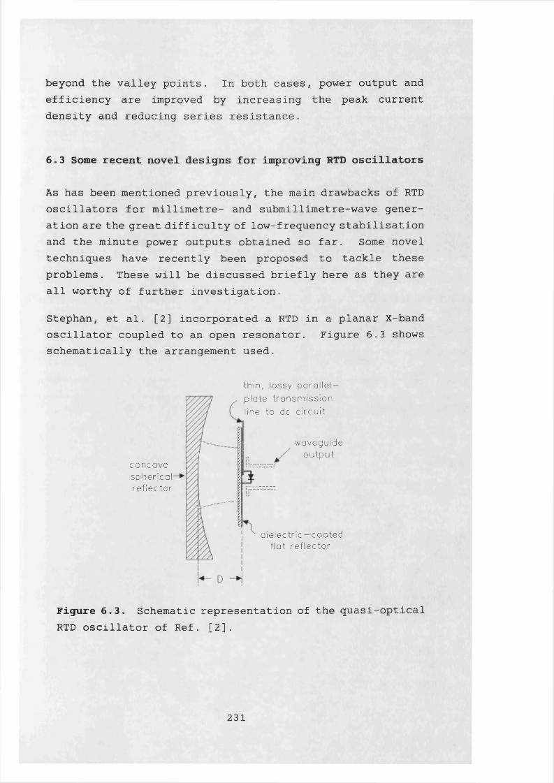
beyond the valley points. In both cases, power output and efficiency are improved by increasing the peak current density and reducing series resistance.
6 .3 Some recent novel designs for improving RTD oscillators
As has been mentioned previously, the main drawbacks of RTD oscillators for millimetre- and submillimetre-wave generation are the great difficulty of low-frequency stabilisation and the minute power outputs obtained so far. Some novel techniques have recently been proposed to tackle these problems. These will be discussed briefly here as they are all worthy of further investigation.
Stephan, et al. [2] incorporated a RTD in a planar X-band oscillator coupled to an open resonator. Figure 6.3 shows schematically the arrangement used.
concavespherical-reflector
thin, lossy parallel — plate transmission line to dc circuit
waveguide output
dielectric—coated flat reflector
Figure 6.3. Schematic representation of the quasi-optical RTD oscillator of Ref. [2].
231
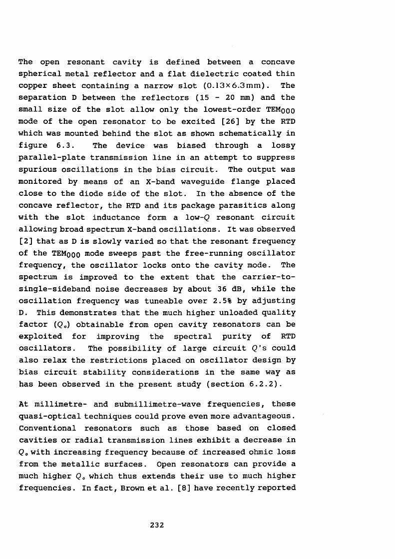
The open resonant cavity is defined between a concave spherical metal reflector and a flat dielectric coated thin copper sheet containing a narrow slot (0.13x6.3mm). The separation D between the reflectors (15 - 20 mm) and the small size of the slot allow only the lowest-order TEMqqq mode of the open resonator to be excited [26] by the RTD which was mounted behind the slot as shown schematically in figure 6.3. The device was biased through a lossy parallel-plate transmission line in an attempt to suppress spurious oscillations in the bias circuit. The output was monitored by means of an X-band waveguide flange placed close to the diode side of the slot. In the absence of the concave reflector, the RTD and its package parasitics along with the slot inductance form a low-Q resonant circuit allowing broad spectrum X-band oscillations. It was observed [2] that as D is slowly varied so that the resonant frequency of the TEMqoo mode sweeps past the free-running oscillator frequency, the oscillator locks onto the cavity mode. The spectrum is improved to the extent that the carrier-to- single-sideband noise decreases by about 36 dB, while the oscillation frequency was tuneable over 2.5% by adjusting D. This demonstrates that the much higher unloaded quality factor (Q0) obtainable from open cavity resonators can be exploited for improving the spectral purity of RTD oscillators. The possibility of large circuit Q ’s could also relax the restrictions placed on oscillator design by bias circuit stability considerations in the same way as has been observed in the present study (section 6 .2 .2 ).
At millimetre- and submillimetre-wave frequencies, these quasi-optical techniques could prove even more advantageous. Conventional resonators such as those based on closed cavities or radial transmission lines exhibit a decrease in Q 0 with increasing frequency because of increased ohmic loss from the metallic surfaces. Open resonators can provide a much higher Q 0 which thus extends their use to much higher frequencies. In fact, Brown et al. [8 ] have recently reported
232
the application of the open resonator in the construction of a millimetre-wave RTD oscillator. They estimate a Q„ of about 1.2X10⁴ at 103 GHz for their resonator which leads to a linewidth of approximately 10 kHz at 10 dB below the peak, an improvement by a factor of 1 0 0 over the same oscillator with a backshort replacing the quasi-optical arrangement.
Despite these and many previous efforts, however, the output powers from RTD oscillators are still too low for most practical applications. Brown et al.'s [8 ] quasi-optically stabilised oscillator has an output of only -19 dBm and at higher frequencies other efforts have reported much lower outputs [7]. Thus, it seems that with the device characteristics currently available the implementation of the RTD oscillator in microwave, millimetre- and submillimetre-wave systems is still not advantageous. However, it is expected that eventually its primary application could be as a low-noise local oscillator for high-sensitivity radiometers operating in the submillimetre-wave region [8 ].
In view of the foregoing, several power-combining schemes have recently been proposed. The classical approach to power combining involves placing a number of sources in a waveguide cavity with separate circuits for each source [27]. At high frequencies, however, this approach becomes impractical and expensive as the components become lossy and difficult to construct. Mink [28] suggested placing devices in a two-dimensional array in a Fabri-Perot cavity in a configuration not unlike that of a laser. Rutlegde, et al. [29] have recently applied this method successfully with planar arrays of 4x4 Gunn diodes and 10x10 MESFET's to obtain effective radiated powers of 22 and 25 W respectively at X-band. As proposed by Stephan [2], this configuration can be applied to RTD's. One such configuration is shown schematically in figure 6.4.
233
bock reflector active grid partially reflecting dielectric slab
Figure 6.4. Schematic representation of a planar monolithic RTD array synchronised by a Fabri-Perot cavity.
The devices could be formed in a monolithic grid pattern on a single GaAs substrate with the bias provided through lossy transmission lines defined on the surface by photolithography. Patch [29] or slot [2] antennas could prove useful techniques in coupling the output from each device to the cavity.
A grid of this type could easily contain hundreds of RTD's thus constituting a planar sheet with a reflection coefficient in excess of unity. The resonator provides feedback that couples the devices together and permits the active sheet to be used as an oscillator. The output from the partially-reflecting dielectric slab could be used directly or coupled into a rectangular waveguide by means of a feedhorn.
Another method of integrating several RTD's to enhance power output has recently been suggested by Yang and Pan [30]. In contrast to the planar integration schemes mentioned previously, Yang and Pan envisage the series integration of several RTD's resulting from growing several double barrier structures on the same substrate. These are separated by thin drift regions sufficient to destroy electron phase coherence between successive RTD's. Now, oscillation cannot be triggered in a circuit consisting of series connected
234
NDR devices unless the dc supply is switched on fast enough [31]. However, when the turn-on process is so fast that capacitive current components dominate, the initial distribution of the total voltage can be equally partitioned among the individual NDR elements and adjusted to reach into the NDR regions of the individual I-V characteristics, providing these are sufficiently similar [31]. Thus, rf oscillation can be initiated and sustained given a proper embedding circuit.
It is estimated that for a series-integrated RTD structure designed to operate in the millimetre-wave region, a turn-on time of the order of 1 ps is required [30]. It may be possible to provide these necessary switching conditions by applying the nonlinear transmission line technique [32] which has resulted in 6V-amplitude voltage shock waves with 1 . 6 ps fall times.
The maximum output power from vertically integrated devices has been shown to be proportional to the square of the number of integrated devices [33]. Yang and Pan estimate that about 0.1 W output at 100 GHz should be possible from 10 series-integrated RTD's, after allowing for 20% spread in peak currents and the degradation due to transit time effects. This is indeed a promising estimate.
235
References1. C. Y. Belhadj, K. P. Martin, S. Ben Amor, J. J. L. Rascol, R. J. Higgins, R. C. Potter, and E. Hempfling, "Bias circuit effects on the current-voltage characteristic of doublebarrier tunneling structures: experimental and theoretical results", Appl. Phys. Lett., Vol. 57, 1990, pp. 58-60.2. K. D. Stephan, E. R. Brown, C. D. Parker, W. D. Goodhue,C. L. Chen, and T. C. L. G. Sollner, "Resonant-tunnelling diode oscillator using a slot-coupled quasioptical open resonator", Electron. Lett., Vol. 27, 1991, pp. 647-649.3. E. R. Brown, T. C. L. G. Sollner, W. D. Goodhue, and C.D. Parker, "Millimeter-band oscillations based on resonant tunneling in a double-barrier diode at room temperature", Appl. Phys. Lett., Vol. 50, 1987, pp. 83-85.4. T. C. L. G. Sollner, E. R. Brown, W. D. Goodhue, and H. Q. Le, "Observation of millimeter-wave oscillations from resonant tunneling diodes and some theoretical considerations of ultimate frequency limits", Appl. Phys. Lett., Vol. 50, 1987, pp. 332-334.5. E. R. Brown, W. D. Goodhue, and T. C. L. G. Sollner, "Fundamental oscillations up to 200 GHz in resonant tunneling diodes and new features of their maximum oscillation frequency from stationary-state tunneling theory", J. Appl. Phys., Vol. 64, 1988, pp. 1519-1529.6 . E. R. Brown, T. C. L. G. Sollner, C. D. Parker, W. D. Goodhue, and C. L. Chen, "Oscillations up to 420 GHz in GaAs/AlAs resonant tunneling diodes", Appl. Phys. Lett., Vol. 55, 1989, pp. 1777-1779.7. E. R. Brown, J. R. Soderstrom, C. D. Parker, L. J. Mahoney, K. M. Molvar, and T. C. McGill, "Oscillations up to 712 Ghz in InAs/AlSb resonant tunneling diodes", Appl. Phys. Lett., Vol. 58, 1991, pp. 2291-2293.8 . E. R. Brown, C. D. Parker, K. M. Molvar, and K. D. Stephan "A quasioptically stabilized resonant-tunneling diode oscillator for millimeter- and submillimeter-wave regions", IEEE Trans. Microwave Theory Tech., Vol. MTT-40, 1992, pp. 846-850.9. T. J. Shewchuk, P. C. Chapin, J. M. Gering, P. D. Coleman, W. Kopp, and H. Morkog, "Microwave admittance characterisation of GaAs-AlxGai-xAs resonant tunneling heterostructures," Proc. IEEE: Cornell Conf. advanced concepts in high speed semiconductor devices and circuits, Cornell University, Ithaca, New York, 1985, pp. 370-379.10. J. M. Gering, D. A. Crim, D. G. Morgan, and P. D. Coleman, "A small-signal equivalent-circuit model for GaAs-AlxGai_xAs resonant tunneling heterostructures at microwave frequencies", J. Appl. Phys, Vol. 61, 1987, pp. 271-276.
236
11. D. Lippens, P. Mounaix, "Small-signal impedance of GaAS-AlxGai_xAs resonant tunnelling heterostructures at microwave frequencies," Electron. Lett., Vol. 24, 1988, pp. 1180-1181.12. J. M. Owens, D. J. Halchin, K. L. Lear, W. S. Lee, and J. S. Harris Jr., "Microwave characteristics of MBE grown resonant tunneling devices," IEEE Int. Microwave Symp. Digest, 1989, pp. 471-474.13. A. Zarea, A. Sellai, M. S. Raven, D. P. Steenson, J. M. Chaimberlain, M. Henini, and 0. H. Hughes, "Small signal analysis of resonant tunnel diodes in the bistable mode," in W. Eccleston arid P. J. Rosser, ed., ESSDERC 90, 20th European Solid State Device Research Conf., Nottingham, IOP Publishing Ltd, 1990, pp. 559-562.14. A. Zarea, A. Sellai, M. S. Raven, D. P. Steenson, J. M. Chaimberlain, M. Henini, and 0. H. Hughes, "Impedance analysis of GaAs/Al (Ga)As resonant tunnelling diodes in the NDR region," Electron. Lett., Vol. 26, 1990, pp. 1522-1523.15. M. F. C. Schemmann, H. C. Heyker, J. J. M. Kwaspen, and Th. G. van de Roer, "Microwave impedance measurements on resonant tunnelling diodes and network model parameter extraction," IEE Proc.-H, Vol. 138, 1991, pp. 248-252.16. R. E. Miles, G. Millington, R. D. Pollard, D. P. Steenson, J. M. Chaimberlain, and M. Henini, "An accurate equivalent circuit model of resonant tunnelling diodes," Electron. Lett., Vol. 27, 1991, pp. 427-428.17. P. H. Siegel, A. R. Kerr, and W. Hwang, "Topics in the optimization of millimeter-wave mixers," NASA Technical Paper 2287, March 1984.18. A. R. Kerr, "A technique for determining the local oscillator waveforms in a microwave mixer," IEEE Trans. Microwave Theory Tech., Vol. MTT-23, pp. 828-831, 1975.19. P. D. Batelaan and M. A. Frerking, "Quantum well multipliers", in R. Temkin (ed.): Proc. 12th Int. Conf. Infrared Millimeter Waves, 1987, paper Ml.7, pp. 14-15.20. T. C. L. G. Sollner, E. R. Brown, W. D. Goodhue, and C. A. Correa, "Harmonic multiplication using resonant tunneling", J. Appl. Phys., Vol. 64, 1988, pp. 4248-4250.21. A. Rydberg and H. Gronqvist, "Quantum-well high-effi- ciency millimetre-wave frequency tripler", Electron. Lett., Vol. 25, 1989, pp. 348-349.22. R. Bouregba, D. Lippens, L. Palmateer, E. Bockenhoff, M. Bogey, J. L. Destombes, and A. Lecluse, "Frequency multiplication using resonant tunnelling diode with output at submillimetre wavelengths", Elrctron. Lett., Vol. 26, 1990, pp. 1804-1805.23. P. D. Batelaan, T. J. Tolmunen, and M. A. Frerking, "Quantum-well diode frequency multipliers: varistor case", IEEE Microwave and Guided Wave Lett., Vol. 2, 1992, pp. 289-291.
237
24. T. C. L. G. Sollner, E. R. Brown, C. D. Praker, and W.D. Goodhue, "High-frequency applications of resonant-tun- neling devices", in J. M. Chamberlain, L. Eaves, and J.-C. Portal, (ed.), "Electronic properties of multilayers and low-dimensional semiconductor structures", Plenum Press, New York, 1990, pp. 283-296.25. T. C. L. G. Sollner, E. R. Brown, and W. D. Goodhue, "Microwave and millimeter-wave resonant tunneling diodes", in F. J. Leonberger, C. H. Lee, F. Capasso, and H. Morkog, (ed.), "Picosecond electronics and optoelectronics II", Springer Series in Electronics and Photonics, Vol. 24, 1987,pp. 102-108.26. R. G. Jones, "Precise dielectric measurements st 35 GHz using an open microwave resonator", Proc. I EE, Vol. 123, 1976, pp. 285-290.27. K. Kurokawa, "The single-cavity multiple-device oscillator", IEEE Trans. Microwave Theory Tech., Vol. MTT-19, 1971, pp. 793-801.28. J. W. Mink, "Quasi-optical power combining of solid-state millimetre-wave sources", IEEE Trans. Microwave Theory Tech., Vol. MTT-34, 1986, pp. 273-279.29. D. B. Rutlegde, Z. B. Popovic, R. M. Weikle, II, M. Kim, K. A. Potter, R. C. Compton, and R. A. York, "Quasi-optical power combining arrays", 1990 IEEE MTT-S, Int. Microwave Symp. Digest, Vol. Ill, pp. 1201-1204.30. C. C. Yang and D. S. Pan, "Theoretical investigations of a proposed series integration of resonant tunneling diodes for millimeter-wave power generation", IEEE Trans. Microwave Theory Tech., Vol. MTT-40, 1992, pp. 434-441.31. Y. I. Voronstov and I. V. Polyakov, "Study of oscillatory processes in circuits with several series-connected tunnel diodes", Radio Eng. Electron. Phys., Vol. 10, 1965, pp. 758-763.32. C. J. Madden, R. Marsland, M. J. W. Rodwell, D. M. Bloom, andY. C. Pao, "Hyperabrupt-doped GaAs nonlinear transmission line for picosecond shock-wave generation", Appl. Phys. Lett., Vol. 54, 1989, pp. 1019-1021.33. D. S. Pan, C. C. Yang, C. F. Jou, and B. Jogai, "Multi-layered heterojunction structure for millimeter wave sources", in H. L. Grubin, K. Hess, G. J. Iafrate, and D. K. Ferry, (ed.), "The Physics of submicron structures", Plenum, New York, 1984.
238
APPENDIX I
DESIGN AND CONSTRUCTION OF THE DC CHARACTERISATIONSTATION
A dc characterisation system was required from an early stage. Such a system was intended primarily for accurate determination of I-V characteristics of devices in the unmounted state.
Wafer-probing facilities were thus seen to be advantageous as such techniques would identify devices with promising characteristics at an early stage before subsequent packaging and bonding, a laborious and time-consuming process. A whisker probing station was therefore designed and constructed. The system was also designed to allow I-V measurements on cooled samples. An attempt to resolve the problem of frost formation on the chip surface at low temperatures involved the design of a special cold stage as described in section 1.1. Subsequent sections describe the characterisation station design as well as the protection electronics and the thermocouple pre-amplifier.
At the start of this project there was available a computer programme designed by Mason and Azari [1] which controlled a programmable voltage source in conjunction with an electrometer for device characterisation. This programme was modified extensively and implemented with the system.
1.1 Device cooling assembly
1.2 The cold stage
Figure 1.1 shows the cold stage which consists of a copper cold arm fitted to a flange at the top. At the head of the
239
arm a circular recess accommodates the sample mount (figure 1.2). Not shown in figure I.2a is an inlet tube for liquid nitrogen.
The middle cover is a circular tufnol ring which bolts to the flange. This houses the probe port, nitrogen inlet and outlet purging tubes and the thermocouple port, apart from delineating the sample chamber. The thermocouple leads pass through a rubber sleeve press-fitted into a brass sleeve which screws into the middle cover; thus ensuring a hermetic seal. The leads then protrude into the sample chamber. They are then bent downward at right angles and the junction fitted into a small hole drilled half way into the circular copper sample mount. A smear of high thermal conductivity paste in the junction hole improves thermal contact.
The top cover bolts to the middle cover and is essentially a viewing window. It consists of two glass plates separated by an evacuated space to minimise heat transfer from the outer to the inner plate and thus limit frosting on the surface of the former.
The whole assembly is then placed into a large polystyrene cup with recesses cut out in the side to accommodate the various protrusions described above (figure 1.3). This, in turn, is then fitted into a small dewar which serves the double purpose of giving the whole assembly mechanical stability and surrounding the cold stage with a liquid nitrogen jacket to further minimise heat exchange.
1.3 The probe assembly
Figure 1.4 shows the probe design. This consists of a support shaft which fits into a micro-manipulator arm. The flange at the end of the shaft mates with the flat end of the sleeve which is threaded to take the probe-end of the support shaft.
240

The probe itself consists of a 1.6mm diameter phosphor-bronze arm, 85mm long, fitted tightly into an axial hole in the support shaft. The other end is threaded to take the probe head (figure 1.4).
241
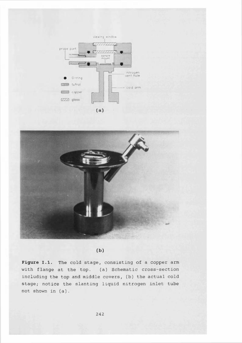
viewing window
probe port
\mmzzzw0m samplemount
nitrogen vent note
• O -ring
V////A tufnolcold arm
copper
(a)
(b)
Figure 1.1. The cold stage, consisting of a copper arm with flange at the top. (a) Schematic cross-section including the top and middle covers, (b) the actual cold stage; notice the slanting liquid nitrogen inlet tube not shown in (a).
242
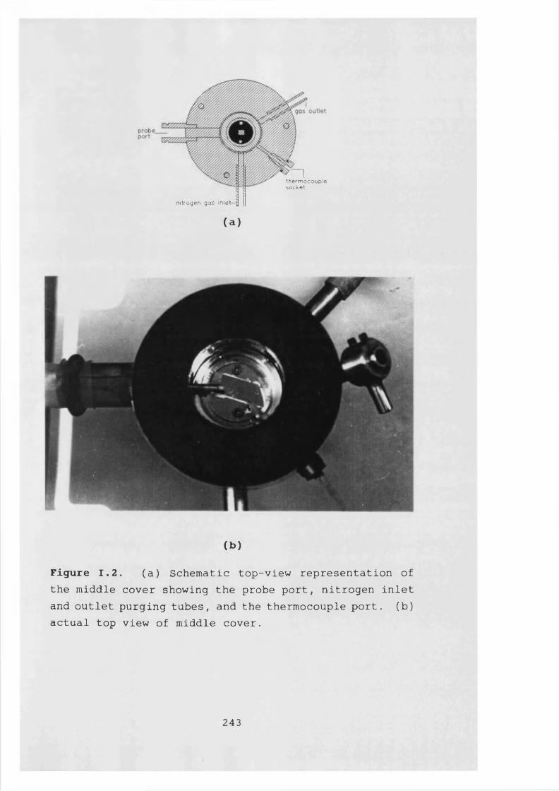
nitrogen gas inlet— )
(a)
thermocouplesocket
(b)
Figure 1.2. (a) Schematic top-view representation ofthe middle cover showing the probe port, nitrogen inlet and outlet purging tubes, and the thermocouple port, (b) actual top view of middle cover.
243
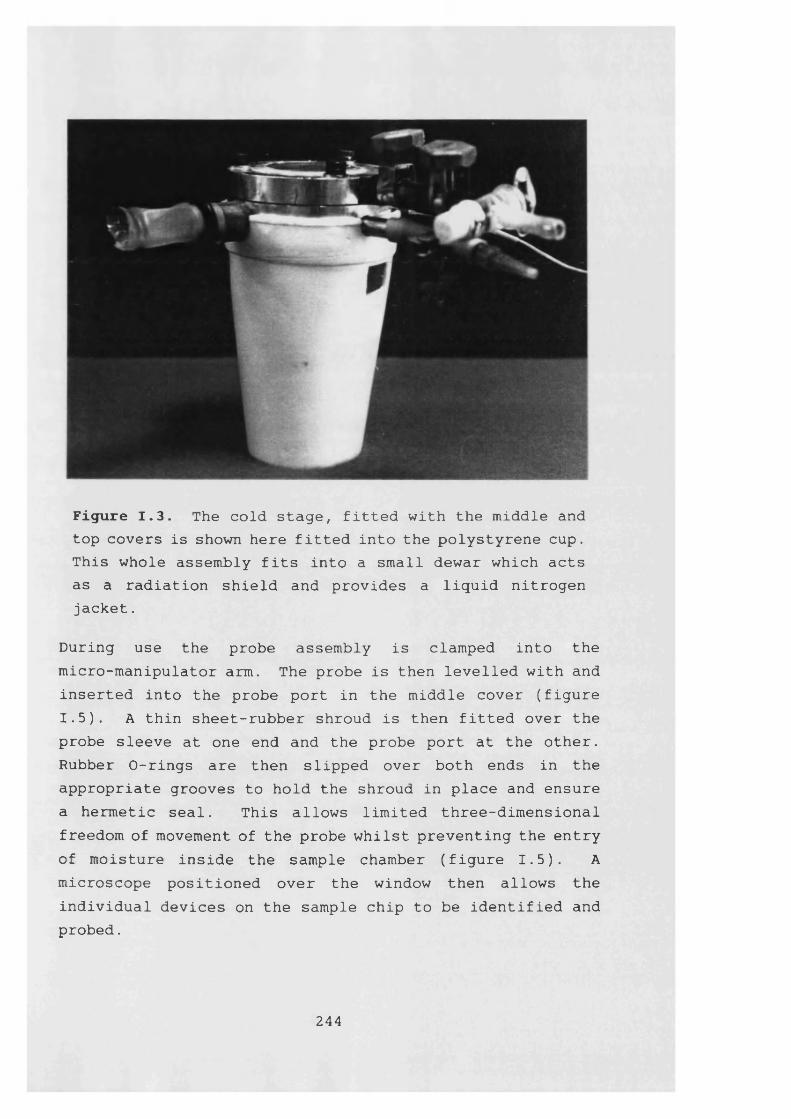
Figure 1.3. The cold stage, fitted with the middle and top covers is shown here fitted into the polystyrene cup. This whole assembly fits into a small dewar which acts as a radiation shield and provides a liquid nitrogen jacket.
During use the probe assembly is clamped into the micro-manipulator arm. The probe is then levelled with and inserted into the probe port in the middle cover (figure 1.5). A thin sheet-rubber shroud is then fitted over the probe sleeve at one end and the probe port at the other. Rubber O-rings are then slipped over both ends in the appropriate grooves to hold the shroud in place and ensure a hermetic seal. This allows limited three-dimensional freedom of movement of the probe whilst preventing the entry of moisture inside the sample chamber (figure 1.5). A microscope positioned over the window then allows the individual devices on the sample chip to be identified and probed.
244
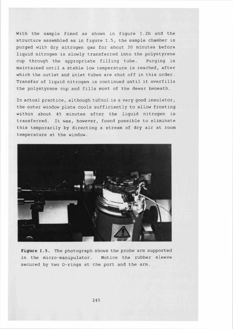
With the sample fixed as shown in figure 1 . 2b and the structure assembled as in figure 1.5, the sample chamber is purged with dry nitrogen gas for about 30 minutes before liquid nitrogen is slowly transferred into the polystyrene cup through the appropriate filling tube. Purging is maintained until a stable low temperature is reached, after which the outlet and inlet tubes are shut off in this order. Transfer of liquid nitrogen is continued until it overfills the polystyrene cup and fills most of the dewar beneath.
In actual practice, although tufnol is a very good insulator, the outer window plate cools sufficiently to allow frosting within about 45 minutes after the liquid nitrogen is transferred. It was, however, found possible to eliminate this temporarily by directing a stream of dry air at room temperature at the window.
Figure 1.5. The photograph shows the probe arm supported in the micro-manipulator. Notice the rubber sleeve secured by two 0-rings at the port and the arm.
245
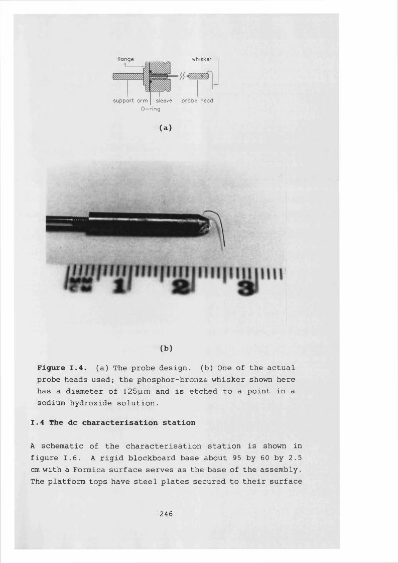
flonge whisker— i
suppo rt a rm sleeve probe head 0 —ring
(a)
(b)
Figure 1.4. (a) The probe design, (b) One of the actualprobe heads used; the phosphor-bronze whisker shown here has a diameter of 125p.m and is etched to a point in a sodium hydroxide solution.
1.4 The dc characterisation station
A schematic of the characterisation station is shown in figure 1.6. A rigid blockboard base about 95 by 60 by 2.5 cm with a Formica surface serves as the base of the assembly. The platform tops have steel plates secured to their surface
246
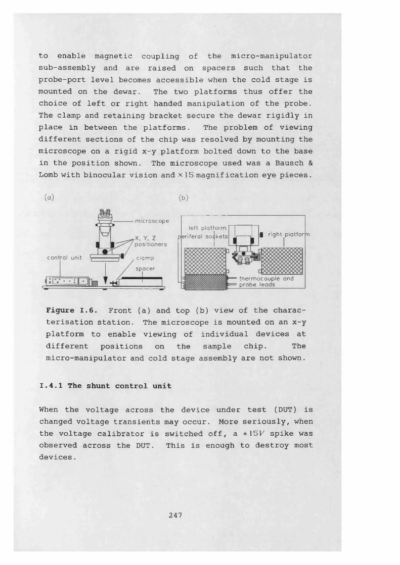
to enable magnetic coupling of the micro-manipulator sub-assembly and are raised on spacers such that the probe-port level becomes accessible when the cold stage is mounted on the dewar. The two platforms thus offer the choice of left or right handed manipulation of the probe. The clamp and retaining bracket secure the dewar rigidly in place in between the platforms. The problem of viewing different sections of the chip was resolved by mounting the microscope on a rigid x-y platform bolted down to the base in the position shown. The microscope used was a Bausch & Lomb with binocular vision and x 15 magnification eye pieces.
(a)
m ic ro s c o p e
p o s itio n e rs
c o n tro l u n it c la m p
spa ce r
( b )
le f t p la t fo rmJ r ig h t p la tfo rmp e r ife ra l so< k e ts
th e rm o c o u p le and p ro b e le od s______
Figure 1.6. Front (a) and top (b) view of the characterisation station. The microscope is mounted on an x-y platform to enable viewing of individual devices at different positions on the sample chip. Themicro-manipulator and cold stage assembly are not shown.
1.4.1 The shunt control unit
When the voltage across the device under test (DUT) is changed voltage transients may occur. More seriously, when the voltage calibrator is switched off, a ±15K spike was observed across the DUT. This is enough to destroy most devices.
247
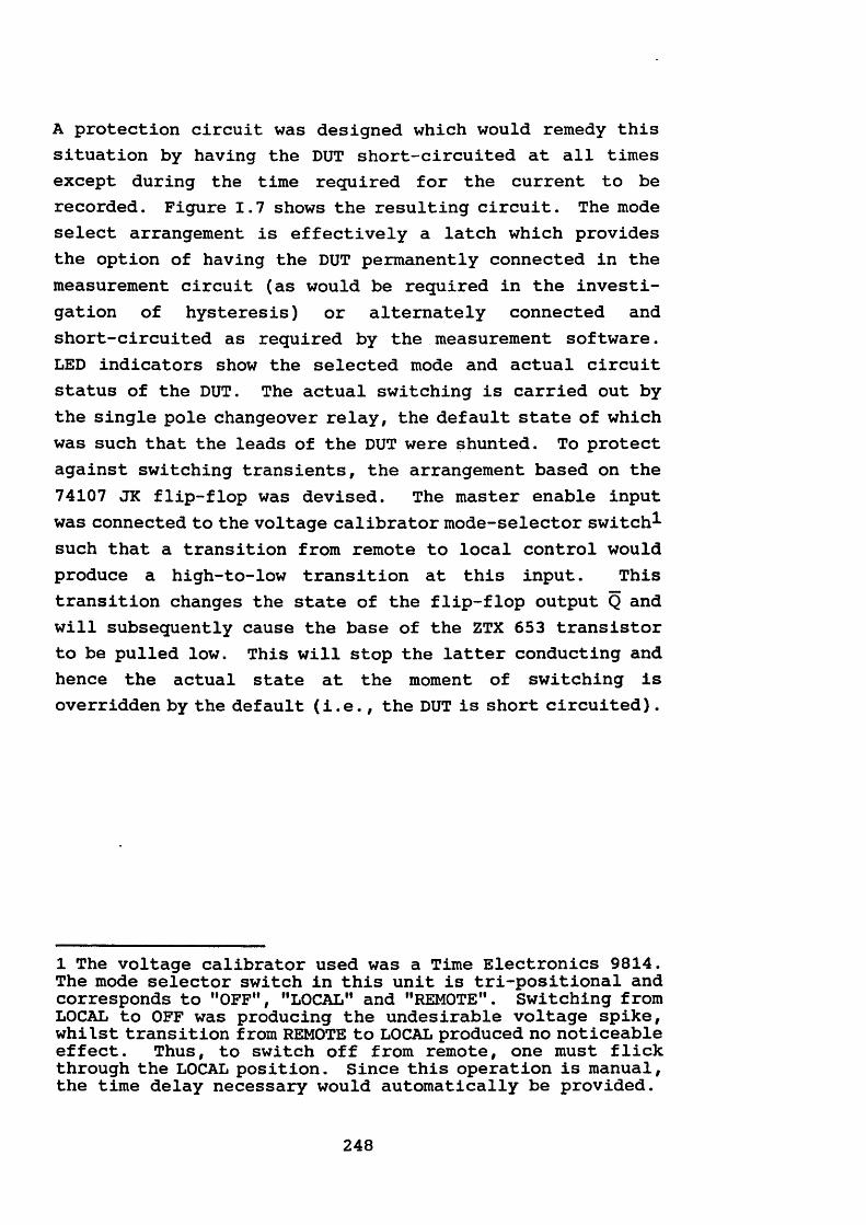
A protection circuit was designed which would remedy this situation by having the DUT short-circuited at all times except during the time required for the current to be recorded. Figure 1.7 shows the resulting circuit. The mode select arrangement is effectively a latch which provides the option of having the DUT permanently connected in the measurement circuit (as would be required in the investigation of hysteresis) or alternately connected and short-circuited as required by the measurement software. LED indicators show the selected mode and actual circuit status of the DUT. The actual switching is carried out by the single pole changeover relay, the default state of which was such that the leads of the DUT were shunted. To protect against switching transients, the arrangement based on the 74107 JK flip-flop was devised. The master enable input was connected to the voltage calibrator mode-selector switch^- such that a transition from remote to local control would produce a high-to-low transition at this input. This transition changes the state of the flip-flop output Q and will subsequently cause the base of the ZTX 653 transistor to be pulled low. This will stop the latter conducting and hence the actual state at the moment of switching is overridden by the default (i.e., the DUT is short circuited).
1 The voltage calibrator used was a Time Electronics 9814. The mode selector switch in this unit is tri-positional and corresponds to "OFF1*, "LOCAL1* and "REMOTE". Switching from LOCAL to OFF was producing the undesirable voltage spike, whilst transition from REMOTE to LOCAL produced no noticeable effect. Thus, to switch off from remote, one must flick through the LOCAL position. Since this operation is manual, the time delay necessary would automatically be provided.
248
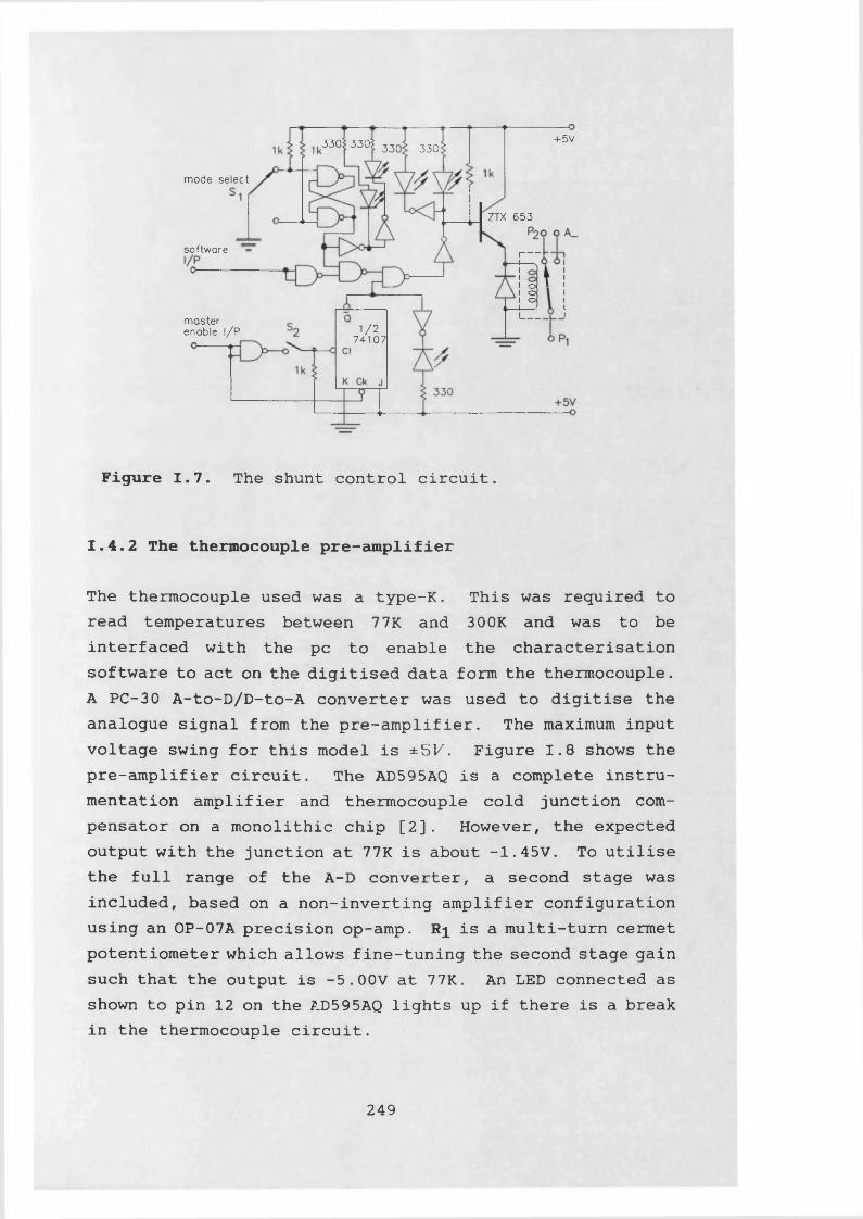
+ 5 V3 3 0 1 3 3 0 1 331 3 3 0 :
mode select
ZTX 6 5 3
software i--i o i o I oI__master
enable l/P 1 /27 4 1 0 7
Figure 1.7. The shunt control circuit.
1.4.2 The thermocouple pre-amplifier
The thermocouple used was a type-K. This was required to read temperatures between 77K and 300K and was to be interfaced with the pc to enable the characterisation software to act on the digitised data form the thermocouple. A PC-30 A-to-D/D-to-A converter was used to digitise the analogue signal from the pre-amplifier. The maximum input voltage swing for this model is ±51/. Figure 1.8 shows the pre-amplifier circuit. The AD595AQ is a complete instrumentation amplifier and thermocouple cold junction compensator on a monolithic chip [2]. However, the expected output with the junction at 77K is about -1.45V. To utilise the full range of the A-D converter, a second stage was included, based on a non-inverting amplifier configuration using an OP-07A precision op-amp. Ri is a multi-turn cermet potentiometer which allows fine-tuning the second stage gain such that the output is -5.00V at 77K. An LED connected as shown to pin 12 on the AD595AQ lights up if there is a break in the thermocouple circuit.
249
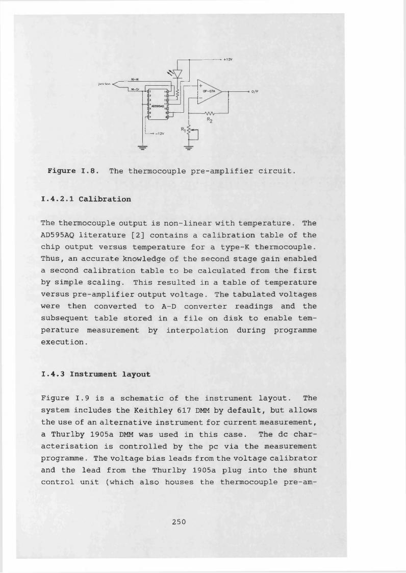
junctionNl-Cr
0/P
° -12V
Figure 1.8. The thermocouple pre-amplifier circuit.
I.4.2.1 Calibration
The thermocouple output is non-linear with temperature. The AD595AQ literature [2] contains a calibration table of the chip output versus temperature for a type-K thermocouple. Thus, an accurate knowledge of the second stage gain enabled a second calibration table to be calculated from the first by simple scaling. This resulted in a table of temperature versus pre-amplifier output voltage. The tabulated voltages were then converted to A-D converter readings and the subsequent table stored in a file on disk to enable temperature measurement by interpolation during programme execution.
1.4.3 Instrument layout
Figure 1.9 is a schematic of the instrument layout. The system includes the Keithley 617 DMM by default, but allows the use of an alternative instrument for current measurement, a Thurlby 1905a DMM was used in this case. The dc characterisation is controlled by the pc via the measurement programme. The voltage bias leads from the voltage calibrator and the lead from the Thurlby 1905a plug into the shunt control unit (which also houses the thermocouple pre-am
250
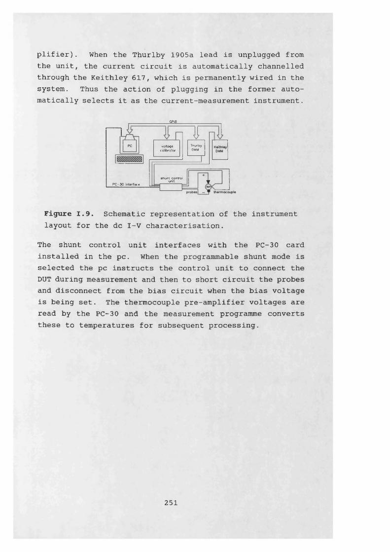
plifier) . When the Thurlby 1905a lead is unplugged from the unit, the current circuit is automatically channelled through the Keithley 617, which is permanently wired in the system. Thus the action of plugging in the former automatically selects it as the current-measurement instrument.
GPIB
shunt control unit
PC-30 interfoce
PC ThurlbyDMMvoltage
calibrator
Figure 1.9. Schematic representation of the instrument layout for the dc I-V characterisation.
The shunt control unit interfaces with the PC-30 card installed in the pc. When the programmable shunt mode is selected the pc instructs the control unit to connect the DUT during measurement and then to short circuit the probes and disconnect from the bias circuit when the bias voltage is being set. The thermocouple pre-amplifier voltages are read by the PC-30 and the measurement programme converts these to temperatures for subsequent processing.
251

References1. H. Mason and J. Azari, unpublished.2. RS Data Library, March 1988, No. 6957, pp. 1-7.
252
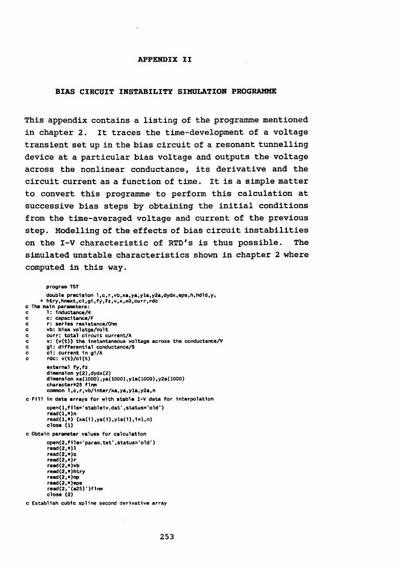
APPENDIX II
BIAS CIRCUIT INSTABILITY SIMULATION PROGRAMME
This appendix contains a listing of the programme mentioned in chapter 2. It traces the time-development of a voltage transient set up in the bias circuit of a resonant tunnelling device at a particular bias voltage and outputs the voltage across the nonlinear conductance, its derivative and the circuit current as a function of time. It is a simple matter to convert this programme to perform this calculation at successive bias steps by obtaining the initial conditions from the time-averaged voltage and current of the previous step. Modelling of the effects of bias circuit instabilities on the I-V characteristic of RTD's is thus possible. The simulated unstable characteristics shown in chapter 2 where computed in this way.
program TSTdouble precision 1,c1r,vb,xa,ya,yla,y2a,dydx>eps,h,hdidly,
+ htry,hnext,c1,g1,fy,fz,v,x,xO,curr,rdc c The main parameters: c 1: 1nductance/Hc c: capac1tance/Fc r: series res1stance/Ohmc vb: bias volatge/Voltc curr: total circuit current/Ac v: (v(t)) the Instantaneous voltage across the conductance/Vc g1: differential conductance/Sc c1: current 1n g1/Ac rdc: v(t)/c1(t)
external fy,fz dimension y(2),dydx(2)dimension xa(1000),ya(1000),yla(1000),y2a(1000) character*25 flnmcommon 1,c,r,vb/1nter/xa,ya,yla,y2a,n
c Fill 1n data arrays for with stable I-V data for Interpolationopen(ltf1le='stab1e1v.dat’,status=‘old’) read(l,*)nread(l,*) (xa(1),ya(1),yla(1),1=l,n) close (1)
c Obtain parameter values for calculationopen(2,f11e=*param.tst',status=’old’)read(2,*)lread(2,*)cread(2,*)rread(2,*)vbread(2,*)htryread(2,*)npread(2,*)epsread(2,'(a25)')flnmclose (2)
c Establish cubic spline second derivative array
253
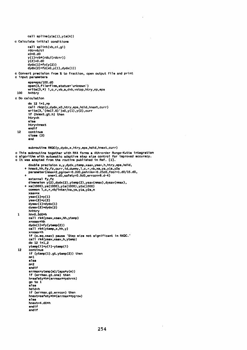
call spHne(yla(l) ,yla(n))c Calculate Initial conditions
call spl1nt(vb,ci,gi)rdc=vb/cix0=0.d0y(1)=vb*(rdc/(rdc+r)) y(2)=0.d0 dydx(l)=fy(y(2)) dydx(2)=fz(x0,yd),dydx(l))
c Convert precision from X to fraction, open output file and print c input parameters
eps=eps/100.d0open(3,file=flnm,status='unknown') wr1te(3,») 1,c,r,vb,a,dvb,vstop,htry,np,eps
100 h=htryc Do calculation
do 12 1*1,npcall rkqc(y,dydx,xO,htry,eps,hdid,hnext,curr)wr1te(3,1(4el7.6)*)x0,y(1),y(2),curr1f (hnext.gt.h) thenhtry=helsehtry=hnext endlf
12 continue close (3) end
subroutine RKQC(y,dydx,x,htry,eps,hdid,hnext,curr)c This subroutine together with RK4 forms a 4th-order Runge-Kutta integration c algorithm with automatic adaptive step size control for improved accuracy, c It was adapted from the routine published 1n Ref. [1].
double precision x,y,dydx,ytemp,xsav,ysav,h,htry,eps,hdid,+ hnext,hh,fy,fz,curr,1d,dummy,1,c,r,vb,xa,ya,yla,y2a
parameter(nmax=2,pg row=-0.2d0,psh rnk=-0.25d0,fco r=1.d0/15.dO,+ one*1.dO,safety=0.9d0,e rrcon=6.d-4)
external fy,fzdimension y(2),dydx(2),ytemp(2),ysav(nmax).dysav(nmax),
+ xa(1000),ya(1000),yla(1000),y2a(1000) common 1,c,r,vb/1nter/xa,ya,yla,y2a,n xsav*x ysav(l)*y(l) ysav(2)=y(2) dysav(l)*dydx(l) dysav(2)=dydx(2) h*htry
1 hh*0.5d0*hcall rk4(ysav,xsav,hh,ytemp) x=xsav+hhdydx(1)*fy(ytemp(2)) call rk4(ytemp,x,hh,y) x=xsav+h1f (x.eq.xsav) pause 'Step size not significant in RKQC.' call rk4(ysav,xsav,h,ytemp) do 12 1*1,2 ytemp(1)=y(1)-ytemp(1>
12 continue1f (ytemp(l).gt.ytemp(2)) thenm=lelsem=2endlfe rrmax*ytemp(m)/(eps*y(m))if (errmax.gt.one) thenh=safety*h*(errmax**pshrnk)go to 1elsehd1d=h1f (errmax.gt.errcon) then hnext=safety* h*(er rmax* *pgrow) elsehnext=4.d0*hendlfendlf
254
cm n
m «D
do 13 1=1,2y(i)=y(i)+ytemp(i)*fcor
13 continuecall splint (y(l),1d,dummy)curr=c*y(2)+1dreturnendsubroutine RK4(y,xO,h,yout)double precision ylxO,yO,hlyoutlzOlykllyk2lyk3lyk4l
+ zkl,zk2,zk3,zk4,fy,fzexternal fy,fz dimension y(2),yout(2) yO=y(D z0=y(2) ykl=h*fy(zO)
I zkl=h*fz(xO,yO,zO) yk2=h*fy(z0+.5d0*zkl)zk2=h*fz(x0+.5d0*h,y0+.5d0*ykl,z0+.5d0*zkl) yk3=h*fy(z0+.5d0*zk2)zk3=h*fz(x0+.5d0*h,y0+.5d0*yk2,z0+.5d0*z k2) yk4=h*fy(z0+zk3)
128 zk4=h*fz(x0+h,y0+yk3,z0+zk3)yout(1)=y0+(ykl+2.dO*yk2+2.dO*yk3+yk4)/6.dOyout(2)=z0+(zkl+2.d0*zk2+2.d0*zk3+zk4)/6.d0returnendsubroutine SPLINE(ypl,ypn)
c This subroutine fits cubic splines to a set of tabulated data. It was c adapted from the routine published 1n Ref. [1]. The common blocks have c been added for ease of handling.
double precision x ly lyl,y2,u,ypl,ypn,p,8lg,qnfun parameter (nmax=1000)dimension x(1000),y(1000),yl(1000),y2(1000),u(nmax)common /1nter/x,y,yl,y2,n1f (ypl.gt..99d30) theny2(l)=0.d0u(l)=0.d0elsey2(l)=-0.5d0u(l)=(3.d0/(x(2)-x(l)))*((y(2)-y(l))/(x(2)-x(l))-ypl)endlfdo 11 1=2,n-ls1g=(x(1)-x(1-l))/(x(1+l)-x(1-l))P=s1g*y2(1-l)+2.d0 y2(1)=(s1g-l.d0)/pu(1)=(6.d0*((y(1+l)-y(1))/(x(1+l)-x(1))-(y(1)-y(1-l))
+ /(x(1)-x(1-l)))/(x(1+l)-x(1-l))-s1g*u(1-l))/pII continue
1f (ypn.gt..99e30) thenqn=0.d0un=0.d0elseqn=0.5d0un=(3.d0/(x(n)-x(n-l)))*
+ (ypn-(y(n)-y(n-l))/(x(n)-x(n-l)))endlfy2(n)=(un-qn*u(n-l))/(qn*y2(n~l)+l.d0) do 12 k=n-l,1,-1 y2(k)=y2(k)*y2(k+l)+u(k)
12 continue return endsubroutine SPLINT(x,y,yl)
c This subroutine performs spline Interpolation and 1s designed to be used c 1n conjunction with SPLINE [1]. It was adapted 1n order to allow derivatives c to be evaluated numerically and output. The common blocks have been added c for ease of handling.
double precision xa,ya,yla,y2a,x,y,yl,h,a,bdimension xa(1000),ya(1000),yla(1000),y2a(1000)common /1nter/xa,ya,yla,y2a,nklo=lkh1=n
1 1f (khl-klo.gt.1) then k=(kh1+klo)/2 if (xa(k).gt.x) then
255
khi=kelseklo=kendifgo to 1endifh=xa(khi)-xa(klo)if (h.eq.O.dO) pause 'Bad XA input in SPLINT.' a=(xa(khi)-x)/h b=(x-xa(klo))/h y=a*ya(klo)+b*ya(khi)++ ((a**3-a)*y2a(klo)+(b**3-b)*y2a(khi))*(h**2)/6.d0yl=(ya(khi)-ya(klo))/h-
+ ((3.d0*(a**2)-l,d0)*y2a(klo)-(3.d0*(b**2)-l.d0)*y2a(khi))*h/6.d0return end
200 double precision function fy(z) c Function subroutine to evaluate dV/dt (=z, in this case).
double precision zfy=zreturnenddouble precision function fz(x,v,z)
c Function subroutine to evaluate d2K/dt2- dz/dL
double precision x,vlz lxa>ya,ylaly2aldcdv>ci,1,c,r,vb,fy,rdccommon 1,c,r,vb/inter/xa,ya,yla,y2a,ndimension xa(1000),ya(1000),yla(1000),y2a(1000)call splint(v,ci,dcdv)rdc=v/c1
211 fz=vb/(l*c)-fy(z)*(dcdv/c+r/l)-v*(r+rdc)/(l*c*rdc) return end
256

References1. W. H. Press, B. P. Flannery, S. A. Teukolsky, and W. T. Vetterling, "Numerical recipes: the art of scientificcomputing", Cambridge University Press, New York, 1987.
257
APPENDIX III
DEVICE PROCESSING AND PACKAGING
III.l Substrate thinning and re-processing
As mentioned previously, some devices were packaged in the LEW Techniques E10/A microwave package. As the substrate thickness of the MOCVD heterostructures was 0.4 mm the wafers had to be thinned down in order to allow their assembly into such small dimensions (see chapter 3). The problem was that these structures had back contact ohmic metallisation and had been previously alloyed at a temperature of 400°C for 12 minutes. This meant that after thinning the wafers, the back contacts would have to be re-formed.
The wafers were diced into 1 x 1 c m 2 chips for ease of handling and fixed face-down onto a manual lapping jig using cya- noacrilate adhesive. The substrate was then lapped down to about 150 - 200 p.m on 1200-grit grinding paper mounted on a flat glass plate. This produced a flat surface with roughness of the order of 20 - 30 n m which promotes adhesion of the ohmic metal to the substrate. The chips were then detached from the lapping jig by dissolving the adhesive in acetone.
The chips were thoroughly cleaned by a 5 minute immersion in boiling acetone followed by another 5 minutes in boiling propanol, after which they were blow-dried under a jet of nitrogen. They were then mounted epilayer face-down on a glass microscope slide using a small quantity of photoresist. The assembly was then placed inside a conventional vacuum coating unit where a Au-Ge (12 at% Ge) layer was evaporated onto the substrate side of the chips to a thickness of about 0.1 p.m. Immersion in acetone removed the chips from the backing plate.
258
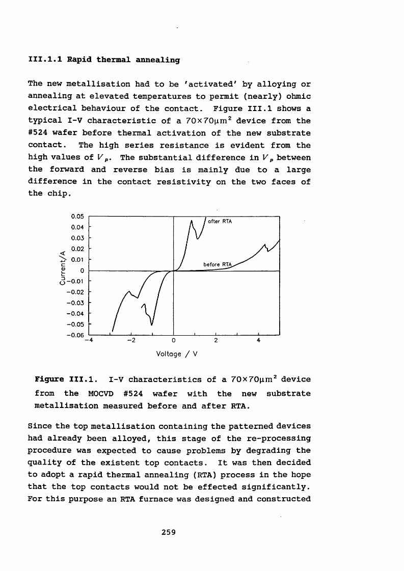
III.1.1 Rapid thermal annealing
The new metallisation had to be 'activated' by alloying or annealing at elevated temperatures to permit (nearly) ohmic electrical behaviour of the contact. Figure III.l shows a typical I-V characteristic of a 70x70pim2 device from the #524 wafer before thermal activation of the new substrate contact. The high series resistance is evident from the high values of K p. The substantial difference ixiVp between the forward and reverse bias is mainly due to a large difference in the contact resistivity on the two faces of the chip.
0.05after RTA
0.04
0.03
0.020.01
before RTA0
- 0.01
- 0.02- 0.03
- 0.04
- 0.05
- 0.06- 4 -2 420
Voltage / V
Figure III.l. I-V characteristics of a 70*70\im2 devicefrom the MOCVD #524 wafer with the new substrate metallisation measured before and after RTA.
Since the top metallisation containing the patterned devices had already been alloyed, this stage of the re-processing procedure was expected to cause problems by degrading the quality of the existent top contacts. It was then decided to adopt a rapid thermal annealing (RTA) process in the hope that the top contacts would not be effected significantly. For this purpose an RTA furnace was designed and constructed
259
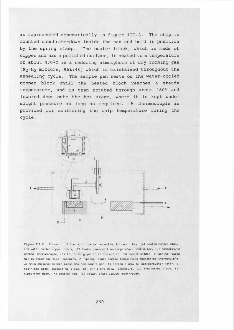
as represented schematically in figure III.2. The chip is mounted substrate-down inside the pan and held in position by the spring clamp. The heater block, which is made of copper and has a polished surface, is heated to a temperature of about 470°C in a reducing atmosphere of dry forming gas (N2-H2 mixture, 96%:4%) which is maintained throughout the annealing cycle. The sample pan rests on the water-cooled copper block until the heated block reaches a steady temperature, and is then rotated through about 180° and lowered down onto the hot stage, where it is kept under slight pressure as long as required. A thermocouple is provided for monitoring the chip temperature during the cycle.
□
Figure III.2. Schematic of the rapid thermal annealing furnace. Key: (A) heated copper block, (B) water-cooled copper block, (C) heater powered from temperature controller, (D) temperature control thermocouple, (E)-(F) forming gas inlet and outlet, (G) sample holder: 1) spring-loaded hollow stainless steel supports, 2) spring-loaded sample temperature-monitoring thermocouple, 3) thin phosphor-bronze press-moulded sample pan, 4) spring clamp, 5) semiconductor wafer, 6) stainless steel supporting plate, (H) air-tight metal enclosure, (I) insulating block, (J) supporting beam, (K) control rod, (L) rotary shaft vacuum leadthrough.
260
When the temperature reaches the maximum desired, the sample is lifted off the hot stage, quickly rotated back over to the cold stage and pressed down to make intimate contact with the polished copper surface of the latter. Water cooling was found necessary since otherwise the cold block temperature would eventually exceed 100°C. This simple design allows excellent, controllable temperature cycles with rise-times comparable to expensive state-of-the-art RTA systems and much shorter fall-times. A typical temperature cycle obtained with the prototype system is shown in figure III.3. It is observed that the temperature rises from an initial 27°C to 370°C in about 3 seconds. The maximum temperature allowed in this particular cycle was 400°C, after which the sample holder was switched to the cooling stage, where a sample temperature drop of 250°C is obtained in the first 2 seconds. The nearly straight portion of the curve between 400 and 370°C on the falling edge corresponds to the switching interval between hot and cold stages.
Different temperature cycles were tried on a number of test chips in order to optimise the process. In each case the original I-V characteristic of a few sample devices were compared with the corresponding characteristics after processing. The optimum cycle which did not result in any significant change was found to be one which allowed the substrate temperature to vary between 380 and 402°C in 21 seconds. The hot stage temperature for this cycle was set at 470°C and the chip was covered with a piece of scrap GaAs wafer of roughly the same area and held in position substrate-down with the spring clamp, as shown in figure III.2.
261
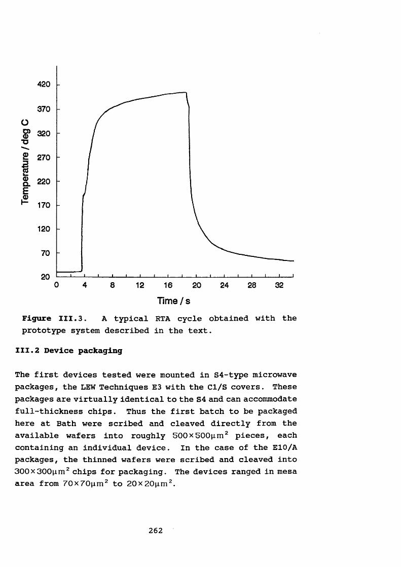
420 -
370O§? 320 TJ
270
120
20 J. 1 10 4 8 12 16 20 24 28 32
T i m e / sFigure III.3. A typical RTA cycle obtained with the prototype system described in the text.
Ill.2 Device packaging
The first devices tested were mounted in S4-type microwave packages, the LEW Techniques E3 with the Cl/S covers. These packages are virtually identical to the S4 and can accommodate full-thickness chips. Thus the first batch to be packaged here at Bath were scribed and cleaved directly from the available wafers into roughly SOOxsOOpim2 pieces, each containing an individual device. In the case of the E10/A packages, the thinned wafers were scribed and cleaved into 300x300p.m2 chips for packaging. The devices ranged in mesa area from 70x70nm2 to 20x20p.m2.
262
The first few chips were fixed to the post with silver-loaded epoxy and cured for 12 hours at a temperature of 80°C followed by 1 hour at 100°C. However the series resistance proved to be appreciably high. Subsequent tests on the epoxy revealed that this was at the root of the problem, as it was probably past its shelf life. It was thus decided to use indium-alloy solder both for attaching the chip and the cover, since this would provide better electrical contacts and result in improved mechanical strength of the completed package.
Indium Corporation of America alloy No. 2 (composition: 80% In, 15% Pb, 5% Ag), with a melting point of 149°C, was used to solder the chip substrate to the gold-plated package post. Thin slices of the solder (which is supplied in the form of -0.6 mm-diameter wire) where cut by means of a scalpel blade and pressed even thinner (~50p.m) between two flat glass sheets. The subsequent flattened dots where diced into rectangular pieces of sides roughly 500p.m for the E3 and 300pim for the E10/A package.
The soldering procedure is delicate and especially tedious with the much smaller E10/A package. Special brass fixing jigs had to be constructed to hold the packages firmly in place for soldering and wire bonding. Both these operations were performed by mounting the fixing jigs on the heated work holder of a West Bond model 7400A ultrasonic wire bonder. The package post is first smeared with a tiny amount of the appropriate flux. A pre-formed piece of indium-alloy solder is then positioned on top of the post and made to flow by setting the work holder temperature to about 160°C. The heat is then turned down and the solder allowed to solidify. The chip is then placed substrate-down on top of the post and centralised. Heat is once more applied until the solder flows. At this point the bonding wedge is brought
263
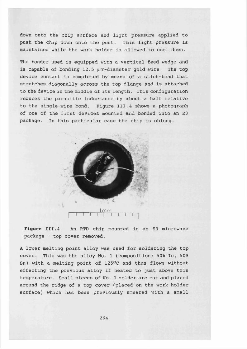
down onto the chip surface and light pressure applied to push the chip down onto the post. This light pressure is maintained while the work holder is allowed to cool down.
The bonder used is equipped with a vertical feed wedge and is capable of bonding 12.5 pm-diameter gold wire. The top device contact is completed by means of a stich-bond that stretches diagonally across the top flange and is attached to the device in the middle of its length. This configuration reduces the parasitic inductance by about a half relative to the single-wire bond. Figure III.4 shows a photograph of one of the first devices mounted and bonded into an E3 package. In this particular case the chip is oblong.
1 m m
Figure III.4. An RTD chip mounted in an E3 microwavepackage - top cover removed.
A lower melting point alloy was used for soldering the top cover. This was the alloy No. 1 (composition: 50% In, 50% Sn) with a melting point of 125°C and thus flows without effecting the previous alloy if heated to just above this temperature. Small pieces of No. 1 solder are cut and placed around the ridge of a top cover (placed on the work holder surface) which has been previously smeared with a small
264
quantity of flux. The E10/A package cover (CIO) is assembled as follows. The work holder temperature is set to about 135°C and the solder allowed to flow. The package flange is next smeared with flux and the cover positioned centrally and held in place until the solder re-flows. The assembled package is then allowed to cool and removed from the fixingjig-
The larger E3 package lids have a top-hat shape. This was exploited in the construction of an assembly tool which allows automatic alignment of the cover with the package flange. In this case a low temperature soldering iron with a narrow tip is used to re-flow the solder and thus fix the top and bottom parts of the package together accurately.
This method of mounting devices was found to be very effective, albeit laborious, as the finished package was mechanically strong and the series resistance introduced found to be negligibly small.
265
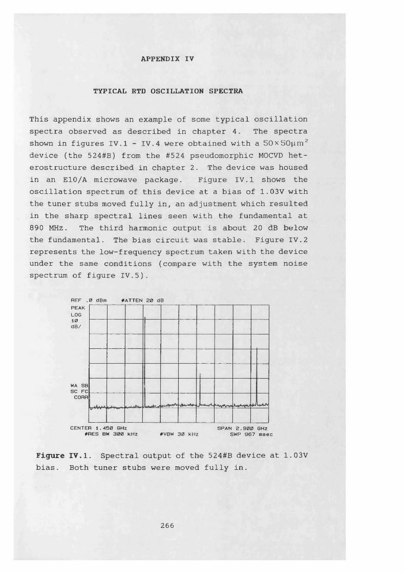
APPENDIX IV
TYPICAL RTD OSCILLATION SPECTRA
This appendix shows an example of some typical oscillation spectra observed as described in chapter 4. The spectra shown in figures IV. 1 - IV. 4 were obtained with a 50x 50pm2 device (the 524#B) from the #524 pseudomorphic MOCVD heterostructure described in chapter 2. The device was housed in an E10/A microwave package. Figure IV. 1 shows the oscillation spectrum of this device at a bias of 1.03V with the tuner stubs moved fully in, an adjustment which resulted in the sharp spectral lines seen with the fundamental at 890 MHz. The third harmonic output is about 20 dB below the fundamental. The bias circuit was stable. Figure IV.2 represents the low-frequency spectrum taken with the device under the same conditions (compare with the system noise spectrum of figure IV.5).
ref .PEAK LOG 10 dB/
WA SB SC FC CORR
CENTER 1.450 GHz SPAN 2.900 GHz#RES BW 300 kHz #VBW 30 kHz SWP 967 msec
Figure IV.1. Spectral output of the 524#B device at 1.03V bias. Both tuner stubs were moved fully in.
0 dBm #ATTEN 20 dB
v
2 6 6
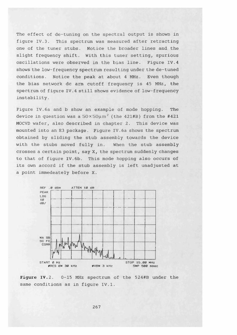
The effect of de-tuning on the spectral output is shown in figure IV.3. This spectrum was measured after retracting one of the tuner stubs. Notice the broader lines and the slight frequency shift. With this tuner setting, spurious oscillations were observed in the bias line. Figure IV.4 shows the low-frequency spectrum resulting under the de-tuned conditions. Notice the peak at about 4 MHz. Even though the bias network dc arm cutoff frequency is 45 MHz, the spectrum of figure IV.4 still shows evidence of low-frequency instability.
Figure IV. 6a and b show an example of mode hopping. The device in question was a 50x50p.m2 (the 421#B) from the #421 MOCVD wafer, also described in chapter 2. This device was mounted into an E3 package. Figure IV.6a shows the spectrum obtained by sliding the stub assembly towards the device with the stubs moved fully in. When the stub assembly crosses a certain point, say X, the spectrum suddenly changes to that of figure IV.6b. This mode hopping also occurs of its own accord if the stub assembly is left unadjusted at a point immedeately before X.
REF .0 dBm ATTEN 10 dBPEAKLOG10dB/
WA SB SC FC CORR
START 0 Hz STOP 15.00 MHz#RES BW 30 kHz #VBW 3 kHz SWP 500 msec
Figure IV. 2. 0-15 MHz spectrum of the 524#B under thesame conditions as in figure IV.1.
267
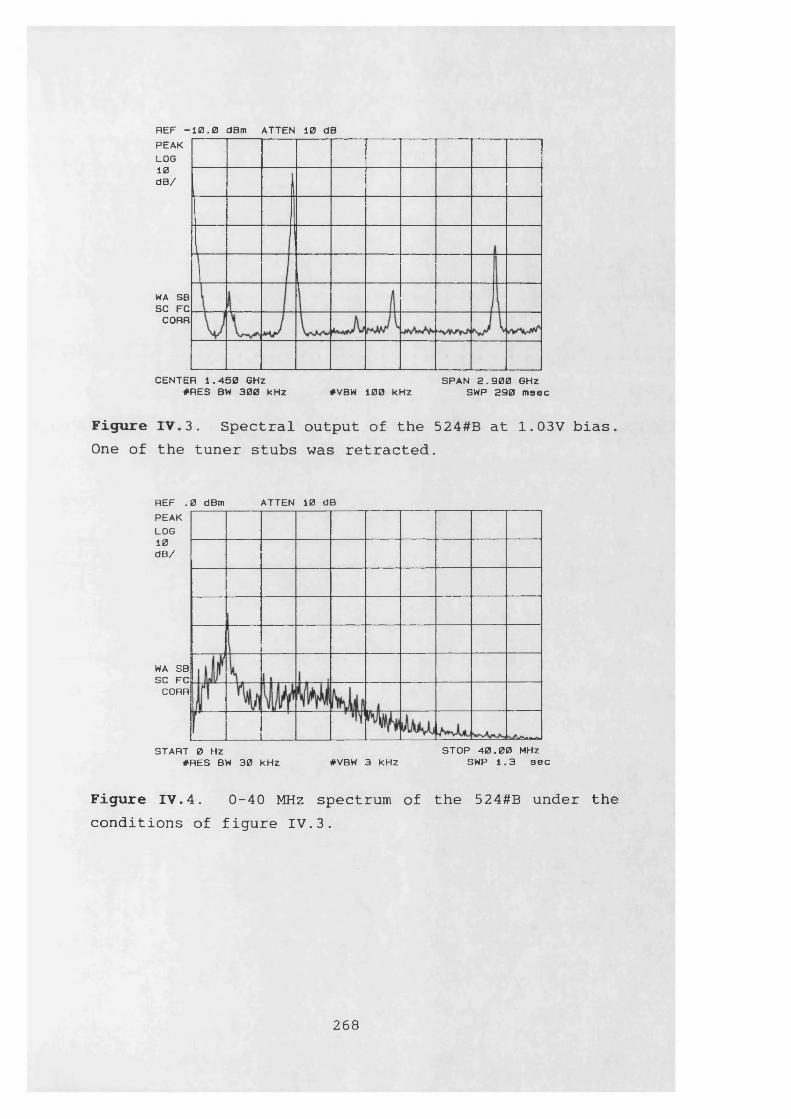
REF -10.0 dBm ATTEN 10 dBPEAKLOG10dB/
WA SB SC FC CORR
CENTER 1.450 GHz#RES BW 300 kHz #VBW 100 kHz
SPAN 2.900 GHz SWP 290 msec
Figure IV.3. Spectral output of the 524#B at 1.03V bias One of the tuner stubs was retracted.
REF .0 dBm ATTEN 10 dBPEAKLOG10dB/
WA SB SC FC CORR
START 0 HZ#RES BW 30 kHz #VBW 3 kHz
STOP 40.00 MHz SWP 1.3 sec
Figure IV.4. 0-40 MHz spectrum of the 524#B under theconditions of figure IV.3.
2 6 8
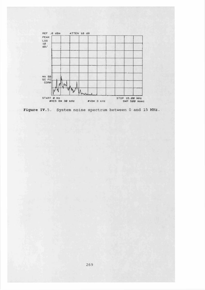
REF .0 dBm ATTEN 10 dBPEAKLOG10dB/
WA SB SC FC CORR
START 0 Hz STOP 15,00 MHz#RES BW 30 kHz #VBW 3 kHz SWP 500 msec
Figure IV.5. System noise spectrum between 0 and 15 MHz.
269
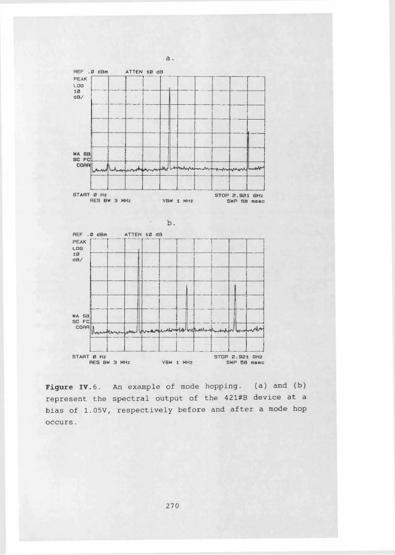
REF .0 dBm PEAK LOG 10 dB/
ATTEN 10 dB
A- 'M./V ~YWW.
START 0 HzRES BW 3 MHz VBW 1 MHz
STOP 2.921 GHz SWP 5B msec
b.REF .0 dBm ATTEN 10 dBPEAK LOG 10 dB/
WA SB SC FC CORR
11I
W v ' A
START 0 HZRES BW 3 MHz VBW 1 MHZ
STOP 2.921 GHz SWP 58 msec
Figure IV.6. An example of mode hopping. (a) and (b) represent the spectral output of the 421#B device at a bias of 1.05V, respectively before and after a mode hop occurs.
270

APPENDIX V
NONLINEAR ANALYSIS PROGRAM
This appendix contains a listing of the nonlinear multiplier analysis program mentioned in chapter 5. The code has not been optimised. Write statements have been omitted, as has the evaluation of multiplier performance in subroutine MLTPER, since these depend upon the intended purpose of any particular version used. The progamme is well commented and the most important variable names have been retained from the original version by Siegel et al. and are explained in chapter 5, which discusses in detail the theory behind the calculations performed.
PROGRAM MULE10A2
C MULTIPLIER ANALYSIS PROGRAM BASED ON P.H.SIEGEL, A.R.KERR, ANDC— W.HWANG, "TOPICS IN THE OPTIMIZATION OF MILLIMETER-WAVE MIXERS",C NASA TECHNICAL PAPER 2287 (MARCH 1984).C THIS VERSION ENABLES ANALYSIS OF MULTIPLIER PERFORMANCE WITH ANC— E10/A - PACKAGED DEVICE IN THE 3.5MM COAXIAL MOUNT DESCRIBED IN C CHAPTER 3.
C BEGIN THE MULTIPLIER ANALYSIS
C FOR COMMON/CONST/:REAL*8 PI INTEGER NINP
C FOR COMMON/DIODE/:REAL*8 RS,FP,WP,VIN(500),IIN(500),GIN(500),CIN(500),DCDVIN(500),
+GIN2(500),CIN2(500),IGJ,ICJ,GJ,CJ C— FOR COMMON/IMPED/:
REAL*8 LOPWR,ZER(16),ZEI(16),ZERDCC FOR COMMON/LOOPS/:
INTEGER NH,NL0,JLO,NVLO,NPTS,NCURR,IPT,NPRINT.NITERC FOR C0MM0N/RKG/:
REAL*8 ACC.VDINIT INTEGER NDIM
C FOR COMMON/TLINE/:REAL*8 ZO.ZQACC INTEGER ZQFLAG
C— FOR COMMON/VOLTS/:COMPLEX*16 VR(16)REAL*8 VRDC,VLO,VDBIAS,IDBIAS,BIAS(1000)
271
INTEGER NBIASC FOR COMMON/MULT/:
INTEGER NIN.NOUT REAL*8 PAVAIL,PABS,POUT
C FOR COMMON/PUMP/:INTEGER NPUMP REAL*8 PMPPWR(200)
C FOR COMMON/MNTPKG/:REAL*8 C(4),L(4)
C— -FOR COMMON/ZMEAS/:COMPLEX*16 ZM(16)REAL*8 CC1,CC2,LW
C THE COMMON BLOCKS USED ARE:COMMON/CONST/PI,NINPCOMMON/DIODE/RS,FP,WP,VIN,IIN,GIN,CIN,DCDVIN,+GIN2,CIN2,IGJ,ICJ,GJ,CJ COMMON/IMPED/LOPWR,ZER,ZEI,ZERDCCOMMON/LOOPS/NH,NLO,JLO,NVLO,NPTS,NCURR,IPT,NPRINT.NITER COMMON/RKG/ACC,VDINIT,NDIM COMMON/TLINE/ZO,ZQACC,ZQFLAGCOMMON/VOLTS/VR, VRDC, VLO, VDBIAS, IDBIAS, NBIAS, BIASCOMMON/MULT/NIN,NOUT,PAVAIL,PABS,POUTCOMMON/PUMP/NPUMP,PMPPWRCOMMON/MNTPKG/C,LCOMMON/ZMEAS/ZM.CC1.CC2,LWCALL DATAIN
C--CALL SPLINE TO OBTAIN SECOND DERIVATIVES OF THE DC CONDUCTANCEC--AND CAPACITANCE WITH RESPECT TO VOLTAGE. THESE ARE REQUIRED BYC--SPLINT, WHICH INTERPOLATES CURRENT, CONDUCTANCE AND CAPACITANCEC VALUES AS REQUESTED IN FCT AND OUTP.
CALL SPLINE(VIN,IIN,NINP,GIN(1).GIN(NINP),GIN2)CALL SPLINE(VIN,CIN,NINP,DCDVIN(1).DCDVIN(NINP),CIN2)
C--CALL LGSIG TO DO THE LARGE SIGNAL ANALYSISCALL LGSIG
END
SUBROUTINE LGSIG
C THE VARIABLES USED IN THIS SUBROUTINE ARE AS FOLLOWS:C--FOR COMMON/CONST/:
REAL*8 PI INTEGER NINP
C— -FOR COMMON/DATA/:REAL*8 ICJDAT(51),IGJDAT(51),CJDATA(51),GJDATA(51)REAL*8 VDDATA(51),IDDATA(51)
C--FOR COMMON/DIODE/:REAL*8 RS,FP,WP,VIN(500),IIN(500),GIN(500),CIN(500),DCDVIN(500), +GIN2(500),CIN2(500),IGJ,ICJ,GJ,CJ
C— FOR COMMON/FOR ITS/:REAL*8 6JCOS(17),GJSIN(17),CJCOS(17),CJSIN(17),VDCOS(17)REAL*8 VDSIN(17),IDCOS(17),IDSIN(17)INTEGER IER
272
C FOR COMMON/IMPED/:REAL*8 LOPWR,ZER(16),ZEI(16),ZERDC
C FOR COMMON/LOOPS/:INTEGER NH,NLO,JLO,NVLO,NPTS,NCURR,IPT,NPRINT.NITER
C FOR COMMOM/MULT/:INTEGER NIN.NOUT REAL*8 PAVAIL,PABS,POUT
C FOR COMMON/RKG/:REAL*8 ACC.VDINIT INTEGER NDIM
C FOR COMMON/TLINE/:REAL*8 ZO.ZQACC INTEGER ZQFLAG
C FOR COMMON/VOLTS/:COMPLEX*16 VR(16)REAL*8 VRDC,VLO,VDBIAS,IDBIAS.BIAS(1000)INTEGER NBIAS
C FOR COtWON/PUMP/:INTEGER NPUMP REAL*8 PMPPWR(200)
C FOR VARIABLES NOT IN ANY COMMON BLOCKS:COMPLEX*16 RH0(16),ZEMB(16),VL(16),ID,VD,ZQ REAL*8 Y(l),DERY(1),PRMT(5),AUX(8,1)REAL*8 VLDC,VOC,RHODC,ZEMBDC,VDCMLT REAL*8 ZQMAG(16),ZQPHA(16)INTEGER IHLF,ITER,JPUMP,JPT,JH.NHP1,NH02,NH02P1 CHARACTER*4Q SPERR
C THE COMMON BLOCKS USED ARE:COMMON/CONST/PI,NINPCOMMON/DATA/ICJDAT,IGJDAT,CJDATA,6JDATA.VDDATA,IDDATA C0MM0N/DI0DE/RS,FP,WP,VIN,IIN,GIN,CIN,DCDVIN,GIN2,CIN2, +IGJ,ICJ,GJ,CJCOMMON/FORITS/GJCOS,GJSIN,CJCOS.CJSIN.VDCOS,VDSIN.IDCOS,IDSIN,IER COMMON/IMPED/LOPWR.ZER.ZEI.ZERDCCOMMON/LOOPS/NH,NLO,JLO,NVLO,NPTS,NCURR,IPT,NPRINT.NITER COMMON/MULT/NIN,NOUT,PAVAIL,PABS,POUT COMMON/RKG/ACC,VDINIT,NDIM COMMON/TLINE/ZO,ZQACC,ZQFLAGCOMMON/VOLTS/VR.VRDC,VLO,VDBIAS,IDBIAS,NBIAS,BIAS COMMON/PUMP/NPUMP,PMPPWR
C SINCE THE FCT AND OUTP SUBPROGRAMS ARE CALLED BY DRKGS THEY MUST BEC DEFINED EXTERNALLY.
EXTERNAL FCT,OUTPC DEFINE SOME USEFUL CONSTANTS
NHP1=NH+1NHD2=NH/2NHD2Pl=NH/2+lWP=2.0D0*PI*FP
C CAL ZEMBED TO FORM THE EMBEDDING IMPEDANCESCALL ZEMBED(ZER.ZEI,FP.NH)
C CALL PRINT1 TO WRITE THE INITIAL CONDITIONSCALL PRINT1(ZEMB,ZERDC,ZEMBDC,ZER.ZEI,PRMT,Y ,DERY,
273
+VDBIAS.NH.NHD2)C OPEN OUTPUT FILE
OPEN(6,FILE=•mult i p .out’,STATUS= * NEW')C— BEGIN THE LOOP OVER THE PUMP POWER, PAVAIL IN WATTS
DO 30 JPUMP=1,NPUMPC BEGIN THE LOOP OVER THE DC BIAS VOLTAGE
DO 20 JVDC=1,NBIAS VDBIAS=BIAS(JVDC)
C SET THE IMPEDANCE AT DC TO ZO TO SPEED THE ANALYSISZEMBDC=ZO
C FORM THE SET OF COMPLEX IMPEDANCES WITH THE SERIES RESISTANCE ADDEDDO 1 JH=1,NH
1 ZEMB(JH)=DCMPLX(ZER(JH)+RS,ZEI(JH))C CALCULATE THE REFLECTION COEFFICIENT OF THE EMBEDDING NETWORK ATC EACH LO HARMONIC
RHODC=(ZEMBDC-ZO)/(ZEMBDC+ZO)DO 13 JH=1,NH
13 RHO(JH)=(ZEMB(JH)-ZO)/(ZEMB(JH)+ZO)PAVAIL=PMPPWR(JPUMP)/1000.ODO
C— -INITIALIZE VARIABLES FOR THE INTEGRATION BY DRKGS VL0=DSQRT(PAVAIL*8.ODO*ZER(NIN))PRMT(1)=O.ODO PRMT(2)=2.0D0*PI PRMT(3)=PRMT(2)/DFL0AT(NPTS)PRMT(4)=ACCY(1)*VDINIT
C--VDBIAS IS THE DC VOLTAGE APPLIED TO THE CIRCUIT IN WHICHC--ZE(0)=Z0. THE TRUE MULTIPLIER BIAS WILL BE FOUND LATER.
VDC=VDBIASC THE INITIAL LEFT AND RIGHT TRAVELING WAVES ON THE TRANSMISSION LINE
DO 2 JH=1,NHVL(JH)»OCMPLX(0.ODO,0.ODO)
2 VR(JH)=DCMPLX(O.ODO,O.ODO)C THE DC TERMS
VLDC=O.ODOVRDC=VDC*ZO/(ZO+ZEMBDC)ITER=0VR(1)=VLO*ZO/(ZEMB(1)+Z0)
C INITIALIZE DRKGS ERROR WEIGHTDERY(1)=1.0D0
C START THE REFLECTION CYCLE3 ITER=ITER+1
C PRINT ONLY AFTER MULTIPLES OF NPRINT CYCLES HAVE BEEN COMPLETEDJPRINT=MOD(ITER,NPRINT)
C SOLVE THE NETWORK STATE EQUATION OVER ONE LO CYCLEC THEN LOOP OVER THE NUMBER OF LO CYCLES TO REACH STEADY STATE
DO 6 JL0=1,NL0 IPT=1DERY(1)=1.0D0CALL DRKGS(PRMT,Y ,DERY,NDIM,IHLF,FCT,OUTP,AUX)
6 CONTINUEC CALL DFORIT TO FORM THE FOURIER COEFFICIENTS OF THE DIODE CURRENT
274
C AND VOLTAGE.CALL DFORIT(VDDATA,NPTS/2,NH,VDCOS,VDSIN,IER)CALL DFORIT(IDDATA,NPTS/2,NH,IDCOS,IDSIN,IER)
C— SET THE FLAG FOR THE CONVERGENCE TESTS ZQFLAG=0
C CALCULATE THE LEFT TRAVELING WAVE ON THE TRANSMISSION LINEC--THE MINUS SIGN COMES FROM THE CONVERSION OF THE TRIGONOMETRICC--FOURIER SERIES REPRESENTATION RETURNED BY DFORIT INTO THE SINGLEC ENDED COMPLEX EXPONENTIAL SERIES REPRESENTATION USED IN THEC LARGE SIGNAL ANALYSIS.
DO 7 JH=1,NHVD=DCMPLX(VDCOS(JH+1),-VDSIN(JH+1))ID=DCMPLX(IDCOS(JH+1),-IDSIN(JH+1))VL(JH)=0.5D0*(VD-ID*Z0)
C--CALCULATE THE IMPEDANCE RATIOS AT EACH PUMP HARMONIC TO DETERMINEC--THE DEGREE OF CONVERGENCE
ZQ=VD/ID/ZEMB(JH)IF(JH.GT.l) GOTO 5
C AT THE PUMP FREQUENCY THE CONVERGENCE PARAMETER IS MODIFIED BY VLOZQ=(VLO-VD)/ID/ZEMB(l)
5 ZQMAG(JH)=CDABS(ZQ)ZQPHA(JH)=DATAN2(DIMAG(ZQ).DREAL(ZQ))*57.2957795100 IF(ZQMAG(JH).GT.1.ODO+ZQACC) ZQFLAG=ZQFLAG+1 IF(ZQMAG(JH).LT.1.ODO-ZQACC) ZQFLAG=ZQFLAG+1
7 CONTINUEC--THE LEFT TRAVELING WAVE AT DC
VLDC=0.5D0*(VDCOS(1)-ZO*IDCOS(1))9 CONTINUE
C THE NEW RIGHT TRAVELING WAVE INCIDENT ON THE DIODEDO 10 JH=2,NH
10 VR(JH)=VL(JH)*RHO(JH)C THE RIGHT TRAVELING WAVE AT DC AND THE FIRST HARMONIC
VR(1)=RHO(1)*VL(1)+VLO*ZO/(ZO+ZEMB(1))VRDC=W10DC*VLDC+VDC*Z0/(ZO+ZEMBDC)
C--WAS THIS THE LAST REFECTION CYCLE ALLOWED?11 IF(ITER.EQ.NITER) GOTO 12
C--HAS THE SOLUTION CONVERGED?IF(ZQFLAG.EQ.O) GOTO 12
C-GO ON TO THE NEXT REFLECTION CYCLEGOTO 3
C UNSCALE THE CAPACITANCE VALUES (THEY WERE SCALED IN SUBROUTINE FCTC-WHICH IS CALLED BY THE DRKGS INTEGRATION ROUTINE).
12 DO 19 JPT=1,NPTS19 CJDATA(JPT)=CJDATA(JPT)/WP
C-FINISH THE ANALYSIS BY OBTAINING THE FOURIER COEFFICIENTS OF THEC-DIODE CONDUCTANCE AND CAPACITANCE.
CALL DF0RIT(6JDATA,NPTS/2,NH,GJCOS,GJSIN,IER)CALL DFORIT(CJDATA,NPTS/2,NH,CJCOS,CJSIN,IER)
C CALL CALBIAS TO CALCULATE THE ACTUAL BIAS VOLTAGE APPLIED (ALLOWINGC-FOR SERIES RESISTANCE)
CALL CALBIAS(VDCOS(1),IDCOS(1),ZERDC,RS,ZO.VDCMLT.VDBIAS)C-CALL MLTPER TO CALCULATE AND PRINT THE MULTIPLIER PERFORMANCE
275
CALL MLTPER(ZER,RS,VDCOS,VDSIN,IDCOS,IDSIN,NHP1,ZQFLAG,FP,VDCMLT)C REPEAT THE ANALYSIS WITH A NEW PUMP POWER
20 CONTINUEC REPEAT THE ANALYSIS WITH A NEW BIAS VOLTAGE
30 CONTINUE RETURN END
SUBROUTINE MLTPER(ZER,RS,VDCOS,VDSIN,IDCOS,IDSIN,NHP1,ZQFLAG,FP,VDBIAS)
C MULTPER CALCULATES THE MULTIPLIER INPUT AND OUTPUT IMPEDANCES, ABSORBEDC--POWER AT THE PUMP FREQUENCY, OUTPUT POWER AT ALL HARMONICS CONSIDERED, ETC.C--ACCORDING TO THE PURPOSE OF THE INVESTIGATION. PRINT STATEMENTS HAVE BEENC OMITTED FOR BREVITY.
COMPLEX*16 ID(17),VD(17),ZIN(17)REAL*8 ZER(1),RS,EFF(17),PABS,PAVAIL,POUT,LOSSDB(16),FP,VDBIAS REAL*8 VDCOS(NHPI).VDSIN(NHPl),IDCOS(NHPl),IDSIN(NHPl),P0DBM(16)INTEGER NIN.NOUT,ZQFLAG COMMON/MULT/NIN,NOUT,PAVAIL,PABS,POUTCOMMON/LOOPS/NH,NLO,JLO,NVLO,NPTS,NCURR,IPT,NPRINT.NITER
C INPUT IMPEDANCESDO 10 1=1,NHVD(I)=DCMPLX(VDCOS(1+1),-VDSIN(1+1))ID(I)=DCMPLX(IDC0S(I+1),-IDSIN(1+1))ZIN(I)=VD(I)/ID(I)+DCMPLX(RS,O.ODO)
10 CONTINUEC ABSORBED POWER
PABS=O.5D0*DREAL(ZIN(NIN)*ID(NIN)*DCONJG(ID(NIN)))C OUTPUT POWER
DO 20 1=2,NHP0UT=0.5D0*ZER(I)*ID(I)*DC0NJG(ID(I))
C AT THIS POINT, POUT CAN BE USED IN CONJUNCTION WITH PABS TO CALCULATEC— -AND PRINT CONVERSION EFFICIENCY AND CONVERSION LOSS IF REQUIRED
20 CONTINUE RETURN END
SUBROUTINE DRKGS(PRMT,Y ,DERY,NDIM,IHLF,FCT,OUTP,AUX)
C--DRKGS IS AN IBM SSP PROGRAM WHICH SOLVES A SYSTEM OF DIFFERENTIALC--EQUATIONS BY THE RUNGE-KUTTA ALGORITHM. IT HAS NOT BEEN ALTEREDC FOR THIS ANALYSIS.
DIMENSION Y(l),DERY(1),AUX(8,1),A(4),B(4),C(4),PRMT(5)DOUBLE PRECISION PRMT,Y,DERY,AUX,A,B,C,X,XEND,H,AJ,BJ,CJ,R1,R2,1DELTEXTERNAL FCT,OUTP DO 1 1=1,NDIM
1 AUX(8,I)=.066666666666666667D0*DERY(I)X=PRMT(1)XEND=PRMT(2)H=PRMT(3)PRMT(5)=0.D0
276
CALL FCT(X,Y,DERY) IF(H*(XEND-X))38,37,2
2 A(1)=.5D0A(2)=.29289321881345248D0A(3)=1.7071067811865475D0A (4)=.1666666666666666700B(1)=2.D0B(2)=1.D0B(3)=1.D0B(4)=2.D0C(1)=.5D0C(2)=.29289321881345248D0C(3)=1.7071067811865475D0C(4)=.5D0DO 3 1=1,NDIMAUX(1,I)=Y(I)AUX(2,I)=DERY(I)AUX(3,I)=0.D0
3 AUX(6,I)=O.DO IREC=0 H=H+H IHLF=-1 ISTEP=0 IEND=0
4 IF((X+H-XEND)*H)7,6,55 H=XEND-X6 IEND=17 CALL OUTP(X,Y,DERY,PRMT)
IF(PRMT(5))40,8,408 ITEST=09 ISTEP=ISTEP+1
J=110 AJ=A(J)
BJ=B(J)CJ=C(J)DO 11 1=1,NDIM R1=H*DERY(I)R2=AJ*(R1-BJ*AUX(6,I))Y(I)=Y(I)+R2R2=R2+R2+R2
11 AUX(6,I)=AUX(6,I)+R2-CJ*R1 IF(J-4)12,15,15
12 J=J+1IF(J-3)13,14,13
13 X=X+.5D0*H14 CALL FCT(X,Y,DERY)
GOTO 1015 IF(ITEST)16,16,2016 DO 17 1=1,NDIM17 AUX(4,I)=Y(I)
ITEST=1ISTEP=ISTEP+ISTEP-2
18 IHLF=IHLF+1 X=X-H H=.5D0*HDO 19 1=1,NDIM Y(I)=AUX(1,I)DERY(I)=AUX(2,I)
19 AUX(6,I)=AUX(3,I)GOTO 9
20 IMOD=ISTEP/2 IF(ISTEP-IM0D-IM0D)21,23,21
21 CALL FCT(X,Y,DERY)DO 22 I=1,NDIM AUX(5,I)=Y(I)
22 AUX(7,I)=DERY(I)GOTO 9
23 DELT=O.DODO 24 1=1,NDIM
24 DELT=DELT+AUX(8,I)*DABS(AUX(4,I)-Y(I)) IF(DELT-PRMT(4))28,28,25
25 IF (IHLF-10)26,36,3626 DO 27 1=1,NDIM27 AUX(4,I)=AUX(5,I)
ISTEP=ISTEP+ISTEP-4X=X-HIEND=0 GOTO 18
28 CALL FCT(X.Y.DERY)DO 29 1=1,NDIM AUX(1,I)=Y(I)AUX(2,I)=DERY(I)AUX(3,I)=AUX(6,I)Y(I)=AUX(5,I)
29 DERY(I)=AUX(7,I)CALL OUTP(X-H,Y,DERY,PRMT) IF(PRMT(5))40,30,40
30 DO 31 1=1,NDIM Y(I)=AUX(1,I)
31 DERY(I)=AUX(2,I)IREC=IHLFIF(IEND)32,32,39
32 IHLF=IHLF-1 ISTEP=ISTEP/2 H=H+HIF(IHLF)4,33,33
33 IM0D=ISTEP/2IF(ISTEP-IMOO-IMOO)4,34,4
34 IF(DELT-,02D0*PRMT(4))35,35,435 IHLF=IHLF-1
ISTEP=ISTEP/2 H=H+HGOTO 4
36 IHLF=11
278
CALL FCT(X,Y,DERY)GOTO 39
37 IHLF=12 GOTO 39
38 IHLF=1339 CALL OUTP(X,Y,DERY,PRMT)40 RETURN
END
SUBROUTINE FCT(X,Y,DERY)
C--FCT IS REQUIRED BY DRKGS AND SETS UP THE NETWORK STATE EQUATION FOR THEC--DIODE AND TRANSMISSION LINE.C--NOTE THAT THE JUNCTION CAPACITANCE HAS BEEN FREQUENCY SCALED BY 2*PI*FPC SO THAT ONE LO CYCLE OCCURS IN 2*PI SECONDS.
C THE VARIABLE TYPES USED IN THIS SUBROUTINE ARE AS FOLLOWS:C FOR COMMON/CONST/:
REAL*8 PI INTEGER NINP
C FOR COMMON/DIODE/:REAL*8 RS,FP,WP,VIN(500),IIN(500),GIN(500),CIN(500),DCDVIN(500),+GIN2(500),CIN2(500),IGJ,ICJ,GJ,CJ
C--FOR COMMON/LOOPS/:INTEGER NH,NLO,JLO,NVLO,NPTS,NCURR,IPT,NPRINT,NITER
C FOR COMMON/TLINE/:REAL*8 ZO.ZQACC INTEGER ZQFLAG
C FOR COMMON/VOLTS/:COMPLEX*16 VR(16)REAL*8 VRDC,VLO,VDBIAS,IDBIAS,BIAS(IOOO)INTEGER NBIAS
C--FOR VARIABLES NOT IN ANY COMMON BLOCKS:REAL*8 X,Y(1),DERY(1),VSREAL*8 CN,SN,CN0,SN0,CN1,SN1,DCAP2INTEGER JH
C--THE COMMON BLOCKS USED ARE:COMMON/CONST/PI,NINPC0MM0N/DI0DE/RS,FP,WP,VIN,IIN,GIN,CIN,DCDVIN,GIN2,CIN2,+IGJ,ICJ,GJ1CJCOMMON/LOOPS/NH,NLO,JLO,NVLO,NPTS.NCURR,IPT,NPRINT,NITER COMMON/TLINE/ZO,ZQACC.ZQFLAGCOMMON/VOLTS/VR,VRDC,VLO.VDBIAS,IDBIAS,NBIAS,BIAS
C--CALCULATE THE TOTAL VOLTAGE ON THE TRANSMISSION LINE INCIDENT ON THE DIODEC--USING A FAST TRIGIGONOMETRIC ALGORITHM TO FIND SINES AND COSINES. THISC--ALGORITHM INCREASES THE SPEED OF THE PROGRAM AND WAS SUGGESTED TO THEC--ORIGINAL AUTHORS BY 0. GRONDIN OF THE UNIVERSITY OF MICHIGAN. IT HAS BEENC--RETAINED IN THE PRESENT VERSION.
279
VS=VRDCSN1=DSIN(X)CN1=DC0S(X)SNO=O.ODOCN0=1.0D0DO 1 JH=1,NHSN=SN1*CN0+CN1*SN0CN=CN1*CN0-SN1*SN0VS=VS+DREAL(VR(JH))*CN-DIMAG(VR(JH))*SN CN0=CN
1 SNO=SNC— -MULTIPLY BY 2 TO CONVERT VS INTO AN EQUIVALENT TRANSMISSION LINEC VOLTAGE SOURCE
VS=VS*2.ODOC INTERPOLATE TO FIND DIODE CAPACITANCE, CONDCTANCE AND CURRENT
IF(DABS(Y(1)).GT.50.D0) Y(1)=DSIGN(50.D0,Y(1))CALL SPLINT(VIN,CIN,CIN2,NINP,Y(1),CJ,DCAP2)CJ=WP*CJCALL SPLINT(VIN,IIN,GIN2,NINP,Y(1),IGJ,GJ)
C DVD/DTDERY(1)=((VS-Y(l))/Z0-IGJ)/CJ
40 RETURN END
SUBROUTINE OUTP(X,Y,DERY,PRMT)
C OUTP IS REQUIRED BY DRKGS AND IS USED TO OUTPUT THE RESULTSC--OF THE INTEGRATION AT THE PROPER POINT ALONG AN LO CYCLE. WHENC--THE X VARIABLE IN THE DRKGS INTEGRATION REACHES THE END OF ANC--INTERVAL OF LENGTH 1/(NPTS-1) THEN ALL THE WAVEFORM DATA (DIODEC--CURRENTS AND VOTAGE) ARE SAVED IN DATA ARRAYS. OTHERWISE THEC INTEGRATION IS ALLOWED TO CONTINUE. THIS ROUTINE IS NEEDED SINCEC DRKGS AUTOMATICALLY HALVES AND DOUBLES THE INTEGRATION STEP SIZEC TO OBTAIN A GIVEN ACCURACY.C THE VARIABLE TYPES USED IN THIS SUBROUTINE ARE AS FOLLOWS:C FOR COMMON/CONST/:
REAL*8 PI INTEGER NINP
C--FOR COMMON/DATA/:REAL*8 ICJDAT(51),IGJDAT(51),CJDATA(51),GJDATA(51)REAL*8 VDDATA(51),IDDATA(51)
C— FOR COMMON/DIODE/:REAL*8 RS,FP,WP,VIN(500),IIN(500),GIN(500),CIN(500),DCDVIN(500), +GIN2(500),CIN2(500),IGJ,ICJ,GJ,CJ
C--FOR COMMON/LOOPS/:INTEGER NH,NLO,J LO,NVLO,NPTS,NCURR,IPT,NPRINT.NITER
C— -FOR VARIABLES NOT IN ANY COMMON BLOCKS:REAL*8 TX,X,Y(1),DERY(1),PRMT(5).DCAP2
C--THE COMMON BLOCKS USED ARE:COMMON/CONST/PI,NINPCOMMON/DATA/ICJDAT,I6JDAT,CJDATA,GJDATA,VDDATA,IDDATA
280
C0MM0N/DI0DE/RS,FP,WP,VIN,IIN,GIN,CIN,DCDVIN,GIN2,CIN2,+IGJ,ICJ,GJ,CJCOMMON/LOOPS/NH,NLO,J LO,NVLO,NPTS,NCURR,IPT,NPRINT,NITER
C TEST X TO SEE IF WE HAVE REACHED THE END OF AN INTERVALTX=X-PRMT(1)-DFLOAT(IPT)*PRMT(3)
C— -DON’T STORE ANYTHING IF THIS IS NOT THE END OF AN LO CYCLE INTERVAL1 IF(DABS(TX).GT.l.OD-7) GOTO 6
C INCREMENT THE LO CYCLE INTERVAL COUNTER2 IPT=IPT+1
C FIND THE DIODE CAPACITANCE, CONDUCTANCE AND THE CURRENT COMPONENTS.CALL SPLINT(VIN,CIN,CIN2ININP,Y(l),CJ,DCAP2)CJ=CJ*WPCALL SPLINT(VIN,IIN,GIN2,NINP,Y(1),IGJ,GJ)ICJ=DERY(1)*CJ
C SAVE THE LAST POINT (NPTS) AS THE FIRST LO CYCLE POINT.IF(IPT-NPTS-I) 3,4,6
3 VDDATA(IPT)=Y(1)IDDATA(IPT)=IGJ+ICJIGJDAT(IPT)=IGJICJDAT(IPT)=ICJGJDATA(IPT)=GJCJDATA(IPT)=CJGOTO 6
4 VDDATA(1)=Y(1)IDDATA(1)=IGJ+ICJ GJDATA(1)=GJ CJDATA(1)=CJ IGJDAT(1)=IGJ ICJDAT(1)=ICJ
6 CONTINUE 40 RETURN
END
SUBROUTINE DFORIT(FNT,N,M,A,B,IER)
C--DFORIT IS A DOUBLE PRECISION VERSION OF FORIT, AN IBM SSP ROUTINEC--THAT PERFORMS A FOURIER ANALYSIS ON A PERIODIC FUNCTION.C--IT COMPUTES THE COEFFICIENTS OF THE TERMS IN THE SERIES WHICHC--IS GIVEN BY: A(1)+SUM(A(N)C0S((N-1)X)+B(N)SIN((N-1)X)) N=2,3,4...C--NOTE THAT THESE SINGLE ENDED SERIES COEFFICIENTS MUST BE CONVERTEDC--INTO THEIR EQUIVALENT COMPLEX DOUBLE ENDED FOURIER COEFFICIENTSC--FOR USE IN THE REST OF THE ANALYSIS. IN DOING SO A(N) BECOMES A(N)/2C--AND B(N) BECOMES -B(N)/2 FOR N>1. FOR N=l, A(N) REMAINS UNCHANGEDC--SINCE THE FACTOR OF 1/2 IS ALREADY INCLUDED IN THE VALUE RETURNEDC--BY THIS ROUTINE (SEE LABEL 100).
C--THE PARAMETERS USED ARE:C--FNT/: TABULATED VALUES OF THE FUNCTION TO BE ANALYSEDC-- NOTE THAT FNT(l) CORRESPONDS TO TIME T=0C--M/: THE MAXIMUM ORDER OF THE HARMONICS TO BE FITTEDC--N/: DEFINES THE INTERVAL OVER WHICH THE POINTS ARE TAKEN. THEC INTERVAL GOES FROM 0 TO 2*PI AND 2N+1 POINTS ARE TAKEN AS DATA.
281
C— -A/: THE FOURIER COSINE COEFFICIENTS C— B/: THE FOURIER SINE COEFFICIENTSC---IER/: THE RESULTANT ERROR MESSAGE CODE WHERE IER=0 MEANS NO ERROR,C-- IER=1 MEANS N IS LESS THAN M, IER=2 MEANS M IS LESS THAN 0
REAL*8 A(1),B(I),FNT(1),CONST REAL*8 C0EF,C,S,C1,S1,AN,FNTZ,U0,U1,U2,Q INTEGER N,M IER=0
20 IF(M) 30,40,40 30 IER=2
RETURN 40 IF(M-N) 60,60,50 50 IER=1
RETURN 60 AN=N
C0EF=2.ODO/(2.ODO*AN+1.ODO)C0NST=3.14159265358979D0*C0EF S1=DSIN(CONST)C1=DC0S(CONST)C=1.0D0 S=0.ODO J=1FNTZ=FNT(1)
70 U2=0.0D0 U1=0.ODO I=2*N+1
75 UO=FNT(I)+2.0DO*C*U1-U2 U2=U1 U1=U0 1=1-1IF(I-l) 80,80,75
80 A(J)=C0EF*(FNTZ+C*U1-U2)B(J)=C0EF*S*U1 IF(J-(M+1)) 90,100,100
90 Q=C1*C-S1*S S=C1*S+S1*C C=Q J=J+1 GO TO 70
100 A(1)=A(1)*0.5D0 RETURN END
SUBROUTINE PRINT1(ZEMB,ZERDC,ZEMBDC,ZER,ZEI,PRMT,Y ,1DERY,VDBIAS,NHARM,NHD2)
C— PRINT1 WRITES THE VALUES OF THE INPUT VARIABLES AND THE INITIALC CONDITIONS FOR THE NONLINEAR ANALYSIS SECTION OF THE PROGRAM. ITS LISTINGC— HAS BEEN OMITTED FOR BREVITY
SUBROUTINE SPLINE(X,Y,N,YP1,YPN,Y2)
282
C-— THIS SUBROUTINE IS LISTED IN APPENDIX II AND IS THUS OMITTED HERE. IN THIS C— CASE NO COMMON BLOCKS ARE USED.
SUBROUTINE SPLINT(XA,YA,Y2A,N,X,Y,Y1,NSP)
C— -THIS SUBROUTINE IS LISTED IN APPENDIX II AND IS THUS OMITTED HERE. IN THIS C CASE NO COMMON BLOCKS ARE USED.
SUBROUTINE CALBIAS(VDO,IDO,ZERDC,RS,ZO.VDCMLT,VDBIAS)
C— CALBIAS CALCULATES THE ACTUAL DC VOLTAGE WHICH SHOULD BE APPLIEDC TO THE MULTIPLIER IN ORDER TO OBTAIN THE DIODE RECTIFIED CURRENTC CALCULATED IN THIS PROGRAMME.
REAL*8 VDO,IDO,ZERDC,RS,ZO,VDCMLT,VDBIASVDCMLT=IDO*(ZERDC+RS-ZO)+VDBIASRETURNEND
SUBROUTINE ZEMBED(ZER,ZEI,FP,NH)
C THIS SUBROUTINE TRANSFORMS MEASURED LOAD IMPEDANCES THROUGHC AN EQUIVALENT CIRCUIT OF THE E10/A PACKAGE AND 3.5mm COAXIAL MOUNTC--AS OBTAINED IN CHAPTER 3. IT THEREFORE CALCULATES THE EMBEDDINGC--IMPEDANCES AT THE PUMP FREQUENCY AND ITS HARMONICS.
C— FOR COMMON/CONST/:REAL*8 PI INTEGER NINP
C FOR COMMON/MNTPKG/:REAL*8 C(4),L(4)
C FOR COMMON/ZMEAS/:COMPLEX*16 ZM(16)REAL*8 CC1,CC2,LW
C THE COMMON BLOCKS USED ARE:COMMON/CONST/PI,NINP COMMON/MNTPKG/C,L COMMON/ZMEAS/ZM,CC1,CC2, LW
C VARIABLES NOT IN ANY COMMON BLOCKS:INTEGER NFREAL*8 FP,W,ZER(16),ZEI(16)COMPLEX*16 Z(0:4),JW
DO 1 NF=1,NHJW=DCMPLX(0.DO,1.DO)*DFLOAT(NF)*FP*2.ODO*PI Z(0)=ZM(NF)DO 2 J=2,1,-1Z(3-J)=JW*L(J)+(JW*C(J)+Z(2-J)**(-1))**(-1)
2 CONTINUEZER(NF)=DREAL(Z(2))ZEI(NF)=DIMAG(Z(2))
1 CONTINUE RETURN END
283
SUBROUTINE DATAIN
C INPUTS ALL THE REQUIRED DATA FOR THE NONLINEAR ANALYSIS.
CHARACTER*70 TITLEC FOR COMMON/CONST/:
REAL*8 PI INTEGER NINP
C FOR COMMON/DIODE/:REAL*8 RS,FP,WP,VIN(500),IIN(500),GIN(500),CIN(500),DCDVIN(500) , +GIN2(500),CIN2(500),IGJ,ICJ,GJ,CJ
C FOR COMMON/IMPED/:REAL*8 L0PWR,ZER(16),ZEI(16),ZERDC
C FOR COMMON/LOOPS/:INTEGER NH,NLO,J LO,NVLO,NPTS,NCURR,IPT,NPRINT,NITER
C-— FOR COMMON/RKG/:REAL*8 ACC.VDINIT INTEGER NDIM
C FOR COMMON/TLINE/:REAL*8 ZO.ZQACC INTEGER ZQFLAG
C FOR COMMON/VOLTS/:COMPLEX*16 VR(16)REAL*8 VRDC,VLO,VDBIAS,IDBIAS,BIAS(1000)INTEGER NBIAS
C FOR COMMON/MNTPKG/:REAL*8 C(4),L(4)
C FOR COMMON/ZMEAS/:COMPLEX*16 ZM(16)REA1*8 CC1,CC2,LW
C FOR COMMON/PUMP/:INTEGER NPUMP REAL*8 PMPPWR(200)
C FOR COMMON/MULT/:INTEGER NIN.NOUT REAL*8 PAVAIL,PABS,POUT
C FOR VARIABLES NOT IN ANY COMMON BLOCKS:REAL*8 ZR,ZI,VSTART,VSTOP,VSTEP
C THE COMMON BLOCKS USED ARE:COMMON/CONST/PI,NINPCOMMON/DIODE/RS, FP, WP, VIN, I IN, GIN, CIN, DCDVIN, GIN2, CIN2, IGJ, ICJ, +GJ.CJCOMMON/IMPED/LOPWR,ZER,ZEI,ZERDCCOMMON/LOOPS/NH, NLO, JLO, NVLO, NPTS, NCURR, IPT, NPRINT, N ITER COMMON/RKG/ACC,VDINIT,NDIM COMMON/TLINE/ZO,ZQACC,ZQFLAGCOMMON/VOLTS/VR,VRDC,VLO,VDBIAS, IDBIAS,NBIAS,BIASCOMMON/MNTPKG/C,LCOMMON/ZMEAS/ZM,CC1,CC2,LWCOMMON/PUMP/NPUMP,PMPPWRCOMMON/MULT/NIN,NOUT,PAVAIL,PABS,POUT
284
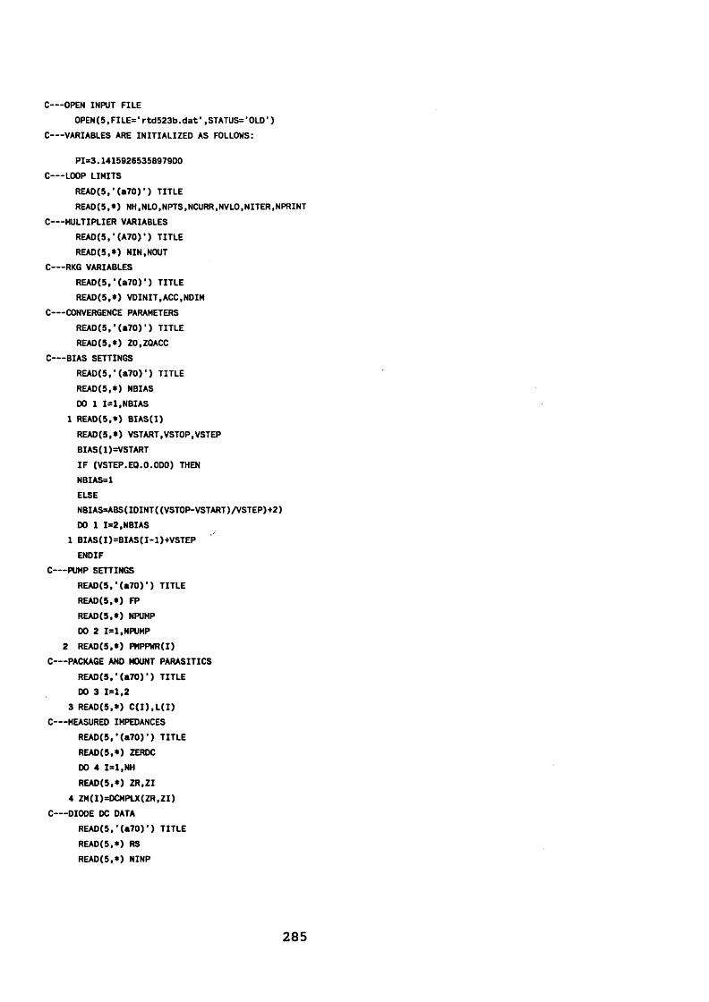
C OPEN INPUT FILEOPEN(5,FILE=‘rtd523b.dat*,STATUS= * OLD')
C— VARIABLES ARE INITIALIZED AS FOLLOWS:
PI=3.1415926535897900C LOOP LIMITS
READ(5t'(a70)’) TITLEREADC5,*) NH,NLO,NPTS,NCURR,NVLO,NITER,NPRINT
C MULTIPLIER VARIABLESREAD(5,*(A70)*) TITLE REA0(5,«) NIN.NOUT
C RKG VARIABLESREAD(5,*(a70)') TITLE READ(5,*) VDINIT,ACC,NDIM
C CONVERGENCE PARAMETERSREAD(5,’(a70)’) TITLE READ(5,*) ZO,ZQACC
C BIAS SETTINGSREAD(5,‘(a70)') TITLE READ(5,*) NBIAS DO 1 1=1,NBIAS
1 READ(5,*) BIAS(I)READ(5,*) VSTART,VSTOP,VSTEPBIAS(1)=VSTARTIF (VSTEP.EQ.O.ODO) THENNBIAS=1ELSENBIAS=ABS(IDINT((VSTOP-VSTART)/VSTEP)+2)DO 1 1=2,NBIAS
1 BIAS(I)=BIAS(I-1)+VSTEP END IF
C PUMP SETTINGSREAD(5,'(a70)’) TITLE READ(5,*) FP READ(5,*) NPUMP DO 2 1=1,NPUMP
2 READ(5,*) PMPPWR(I)C PACKAGE AND MOUNT PARASITICS
READ(5,1(a70)*) TITLE DO 3 1=1,2
3 READ(5,*) C(I),L(I)C MEASURED IMPEDANCES
READ(5,’(a70)’) TITLE READ(5,*) ZERDC DO 4 1=1,NH READ(5,*) ZR,ZI
4 ZM(I)=DCMPLX(ZR,ZI)C DIODE DC DATA
READ(5,'(a70)’) TITLE READ(5,*) RS READ(5,*) NINP
285

DO 5 1=1,NINPREAD(5,*) VIN(I),IIN(I),GIN(I),CIN(I),DCDVIN(I)
5 CONTINUE
CLOSE(5)RETURNEND
286
ACKNOWLEDGMENTS
I am deeply indebted to my supervisor, Dr N. J. Cronin, who was responsible for the conception of this project as well as seeking and obtaining the collaboration of Philips Research Laboratories (PRL), Redhill, and DRA (formerly RSRE), Malvern. His dedication, genuine friendship and expertise have tipped the balance in my favour in many difficult situations of both personal and technical nature.
The realisation of this project would not have been possible without the provision of test devices. In this respect, I am therefore thankful to both Dr J. J. Harris (formerly with PRL) of Imperial College, London, and Dr A. W. Higgs of DRA for supervising the collaborative work on the part of their organisations and for many helpful and enlightening discussions. Thanks are also due to Dr J. M. Chamberlain, D. P. Steenson and M. Henini of Nottingham University for providing sample devices, experimental results of which could not, unfortunately, feature in this thesis for the sake of brevity. I am especially grateful to Dr S. J. Bending for providing the MOCVD structures. His resourcefulness, genuine interest in the work and many helpful suggestions have made possible the device processing and bonding. I am grateful to my friend and colleague, Mr A. S. Treen for his advice on device processing and numerous fruitful discussions, and to Dr A. Wright for the transmission electron micrography of the strained-layer structures.
This project involved a considerable element of technical design and construction. In this respect I am especially grateful to Mr R. C. J. Draper without whose technical
287
support, advice and know-how much of the hardware construction would not have been possible. I would also like to thank Mr Draper for the photographs appearing in this report and Mr M. Deven of the School of Materials Science for the E3 package negatives.
Unfortunately, it is not possible to specifically mention everyone who helped directly or indirectly during the fruitful years I have spent working at the School of Physics, Bath University. I therefore express my gratitude to all the members of the academic, technical and non-technical staff of this School who have assisted me in any way.
Finally, I wish to acknowledge the financial support of the British Council and thank the Association of Commonwealth Universities for the award of the fellowship which led to this project, and the University of Malta for granting the necessary study leave.
288


