Embed Size (px)
Citation preview
CE1921: COMPUTER ARCHITECTURE SINGLE-CYCLE PROCESSOR DESIGN
Dr. Russ Meier, Milwaukee School of Engineering, Last Update: April 9, 2019
SUMMARY
Instruction set architecture describes the programmer’s view of the machine. This level of computer blueprinting allows design engineers to discover expected features of the circuit including:
data processing instructions like ADD, SUB, AND, EOR, etc., memory load-store instructions like LDR, STR, etc., branch instructions with both conditional and unconditional flow control, the names and sizes of the registers provided for computational storage and flow control, the size of data memory provided for longer term storage during program execution, and the binary encodings for each instruction.
These features are then used by design engineers as they choose components to organize together into a working circuit. Multiple micro-architectures are possible for any given instruction set architecture because different design engineers can choose different components and different organizational strategies when implementing the features. In the end, however, any micro-architecture design must implement the features described by the instruction set architecture.
One organizational decision that leads to different micro-architectures is the number of clock periods used per instruction. Three common clock-period strategies are called single-cycle, multi-cycle, and pipelined.
Single-cycle processors use one clock-period per instruction and the clock-period is set by the total delay of the slowest instruction. This is a disadvantage because a faster instruction cannot execute more quickly. The advantage, however, is straightforward control circuitry.
Multi-cycle processors use multiple clock-periods per instruction and each instruction uses the minimum number of clock periods required for its execution. This allows faster instructions that do not access data memory, like ADD, to avoid the unnecessary delay of the data memory stage. Thus, the advantage is speed for faster instructions. The disadvantage is more complex control because a finite state machine controller must be built to coordinate control signals across multiple clock periods.
Pipelined processors exploit instruction level parallelism to allow multiple instructions to be in execution at the same time. This is accomplished by adding state registers between the instruction fetch, instruction decode, execute, memory access, and write-back stages of the circuit.
This multi-week project requires students to design and simulate a single-cycle processor for a subset of the ARMv4 instructions. Students are required to:
Design VHDL and schematic components. Organize the components together into a top-level schematic that implements a single-cycle processor. Simulate the processor using a basic test program.
CE1921: COMPUTER ARCHITECTURE SINGLE-CYCLE PROCESSOR DESIGN
Dr. Russ Meier, Milwaukee School of Engineering, Last Update: April 9, 2019
SUMMARY Instruction set architectures can be implemented in multiple ways. An organization of components into a circuit capable of executing instructions forms a micro-architecture. The textbook presents one micro-architecture that follows the ARMv4 instruction set architecture quite closely. In the textbook micro-architecture, a partial branch address of PC+8 is formed by an adder and routed to the register file on each clock cycle. This allows the controller to route PC+8 to the A input of the ALU to finish adding the left-shifted immediate to form the full branch address as PC+8 + (SExtImm32 << 2). The textbook also presents a more complex controller that coordinates conditional instruction execution.
An alternate organization is presented in this laboratory. This organization simplifies the register file and the control logic for branching. The partial branch address is removed from the register file and replaced by a separate circuit that calculates the full branch address without using the ALU. The instruction set implemented by the controller is kept to a foundational set of ARMv4 instructions. The basic arithmetic and logic instructions are included. No conditional versions of these instructions are implemented (i.e. ADDS, SUBS, etc. are not implemented). Simple immediate-offset mode LDR and STR are implemented. Basic branches are implemented but more complex branches are not implemented. This reduced set results in a simpler controller that can be implemented quite cleanly using VHDL when-else statements for each control signal.
Always remember that engineering is both art and science. Through lecture, you have studied the ARMv4 instruction set architecture and basic assembly language programming. You have learned the computer science behind this numeric processor. You can see the art of engineering by studying both the textbook implementation and this laboratory implementation. Both achieve the desired goal of allowing a small set of ARMv4 machine code instructions to execute. But, both achieve the goal using different organizations of components. The choices made in this week’s alternate laboratory organization prevent the processor from executing some ARM instructions that would be expected to work if presented as machine code instructions in a commercial processor. In particular, the LDR and STR instructions are greatly reduced in functionality. In the next laboratory, you will extend the single-cycle processor complexity so that a broader set of instructions will execute.
PROJECT CREATION
Create a new Quartus project for your single-cycle processor named scp. Copy and paste the VHDL of all data path components completed in earlier labs into this new project. Set an advanced synthesis option:
o AssignmentsSettings…Compiler SettingsAdvanced Settings (Synthesis) Block Design Naming Choose Quartus II
o This assignment allows signal busses in block diagram files to use the bracket [ ] syntax (example: D[13..0]). This option used to be the default. More recent versions of Quartus have changed to a different default option.
Complete the exercises that follow.
IMPORTANT NOTE
USE START ANALYSIS AND SYNTHESIS THROUGHOUT YOUR WORK. DO NOT ATTEMPT A FULL COMPILATION TO FPGA.
CE1921: COMPUTER ARCHITECTURE SINGLE-CYCLE PROCESSOR DESIGN
Dr. Russ Meier, Milwaukee School of Engineering, Last Update: April 9, 2019
WEEEK 8 DELIVERABLES The deliverables include:
VHDL descriptions of the remaining data path components, schematic designs of fetch, decode, execute, memory, and write-back circuitry, schematic design of the final single-cycle processor, and testing of the final single-cycle processor.
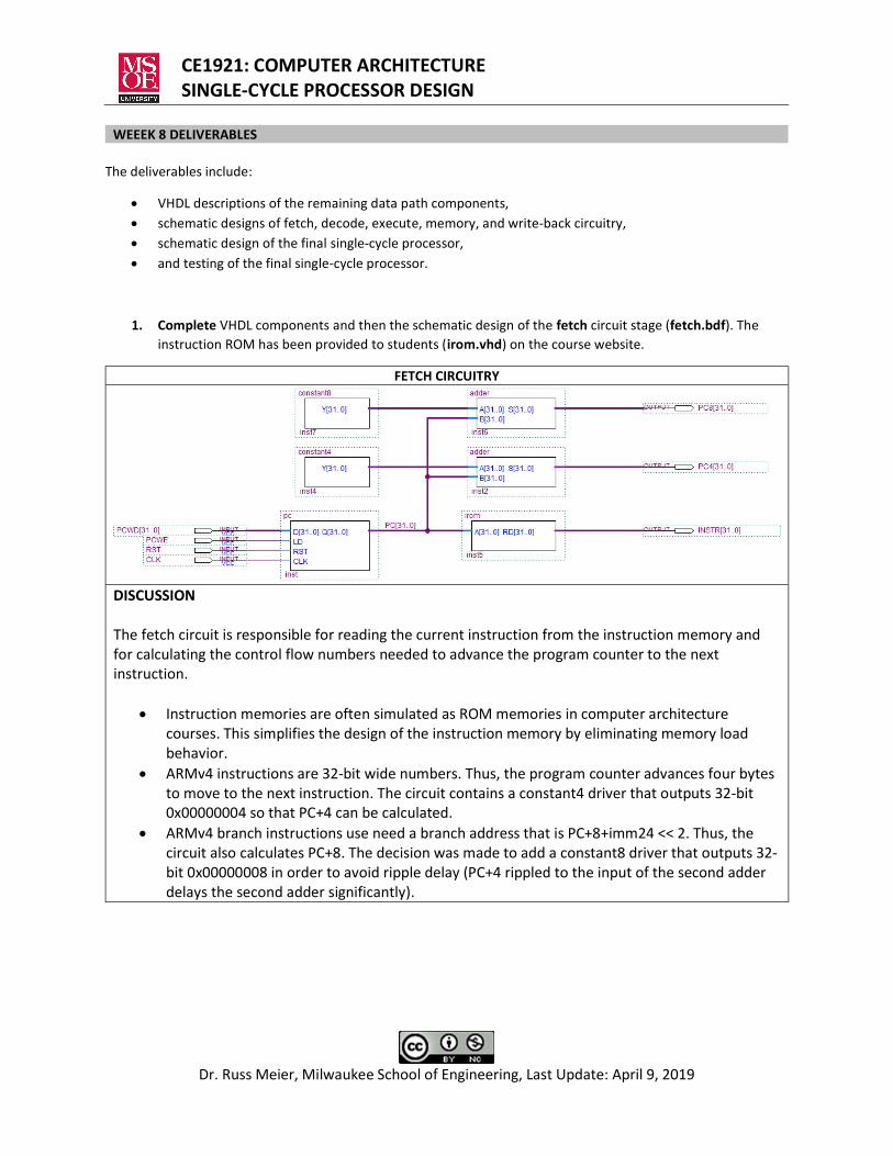
1. Complete VHDL components and then the schematic design of the fetch circuit stage (fetch.bdf). The instruction ROM has been provided to students (irom.vhd) on the course website.
FETCH CIRCUITRY
DISCUSSION The fetch circuit is responsible for reading the current instruction from the instruction memory and for calculating the control flow numbers needed to advance the program counter to the next instruction.
Instruction memories are often simulated as ROM memories in computer architecture courses. This simplifies the design of the instruction memory by eliminating memory load behavior.
ARMv4 instructions are 32-bit wide numbers. Thus, the program counter advances four bytes to move to the next instruction. The circuit contains a constant4 driver that outputs 32-bit 0x00000004 so that PC+4 can be calculated.
ARMv4 branch instructions use need a branch address that is PC+8+imm24 << 2. Thus, the circuit also calculates PC+8. The decision was made to add a constant8 driver that outputs 32-bit 0x00000008 in order to avoid ripple delay (PC+4 rippled to the input of the second adder delays the second adder significantly).
CE1921: COMPUTER ARCHITECTURE SINGLE-CYCLE PROCESSOR DESIGN
Dr. Russ Meier, Milwaukee School of Engineering, Last Update: April 9, 2019
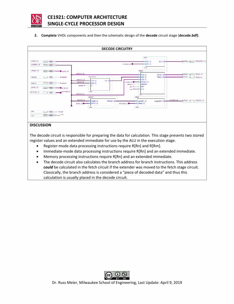
2. Complete VHDL components and then the schematic design of the decode circuit stage (decode.bdf).
DECODE CIRCUITRY
DISCUSSION The decode circuit is responsible for preparing the data for calculation. This stage presents two stored register values and an extended immediate for use by the ALU in the execution stage.
Register-mode data processing instructions require R[Rn] and R[Rm]. Immediate-mode data processing instructions require R[Rn] and an extended immediate. Memory processing instructions require R[Rn] and an extended immediate. The decode circuit also calculates the branch address for branch instructions. This address
could be calculated in the fetch circuit if the extender was moved to the fetch stage circuit. Classically, the branch address is considered a “piece of decoded data” and thus this calculation is usually placed in the decode circuit.
CE1921: COMPUTER ARCHITECTURE SINGLE-CYCLE PROCESSOR DESIGN
Dr. Russ Meier, Milwaukee School of Engineering, Last Update: April 9, 2019
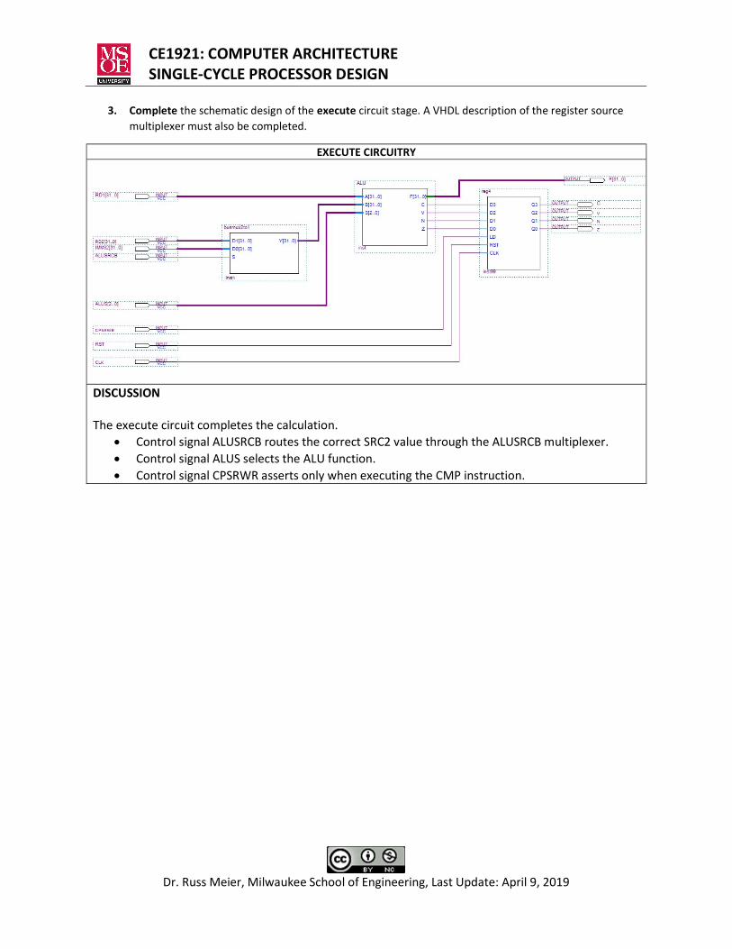
3. Complete the schematic design of the execute circuit stage. A VHDL description of the register source multiplexer must also be completed.
EXECUTE CIRCUITRY
DISCUSSION The execute circuit completes the calculation.
Control signal ALUSRCB routes the correct SRC2 value through the ALUSRCB multiplexer. Control signal ALUS selects the ALU function. Control signal CPSRWR asserts only when executing the CMP instruction.
CE1921: COMPUTER ARCHITECTURE SINGLE-CYCLE PROCESSOR DESIGN
Dr. Russ Meier, Milwaukee School of Engineering, Last Update: April 9, 2019
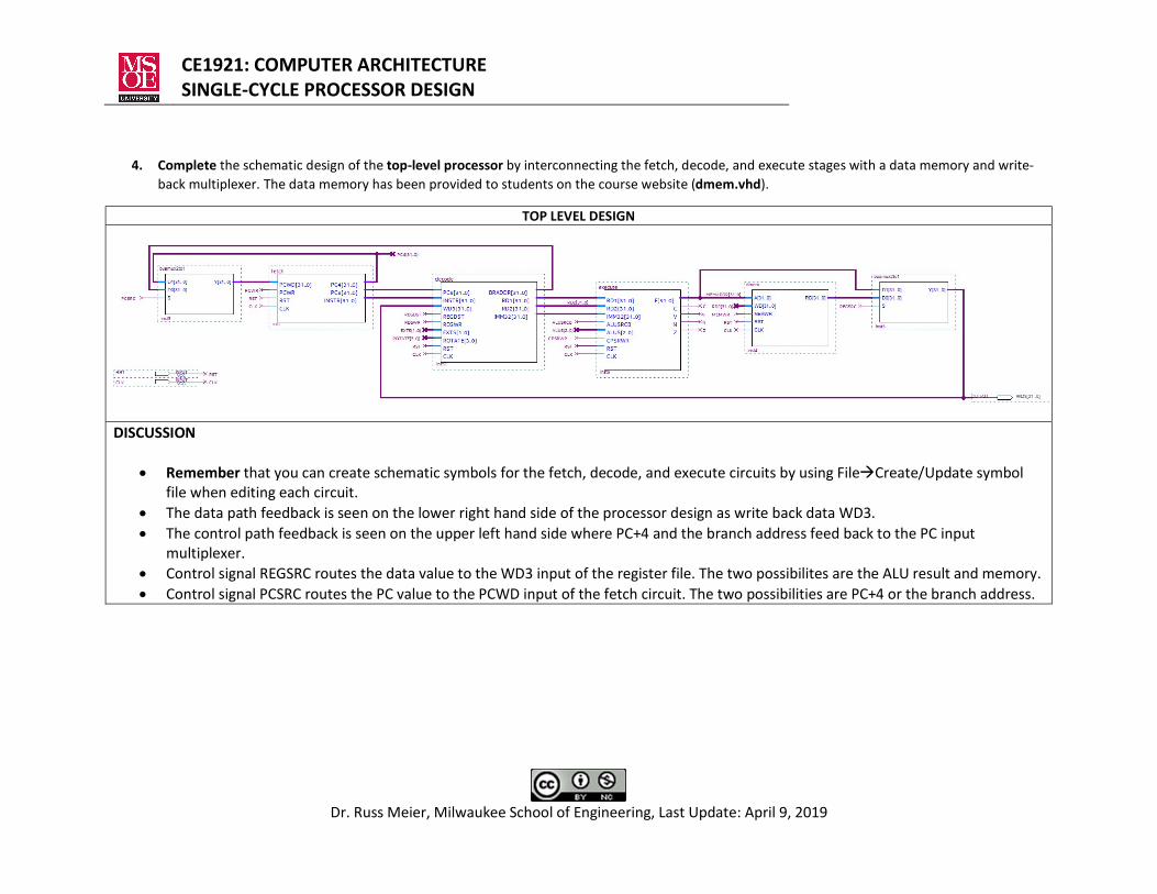
4. Complete the schematic design of the top-level processor by interconnecting the fetch, decode, and execute stages with a data memory and write-back multiplexer. The data memory has been provided to students on the course website (dmem.vhd).
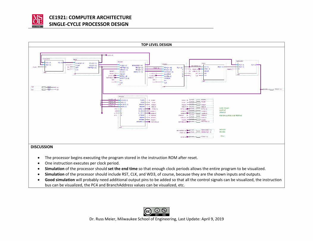
TOP LEVEL DESIGN
DISCUSSION
Remember that you can create schematic symbols for the fetch, decode, and execute circuits by using FileCreate/Update symbol file when editing each circuit.
The data path feedback is seen on the lower right hand side of the processor design as write back data WD3. The control path feedback is seen on the upper left hand side where PC+4 and the branch address feed back to the PC input
multiplexer. Control signal REGSRC routes the data value to the WD3 input of the register file. The two possibilites are the ALU result and memory. Control signal PCSRC routes the PC value to the PCWD input of the fetch circuit. The two possibilities are PC+4 or the branch address.
CE1921: COMPUTER ARCHITECTURE SINGLE-CYCLE PROCESSOR DESIGN
Dr. Russ Meier, Milwaukee School of Engineering, Last Update: April 9, 2019
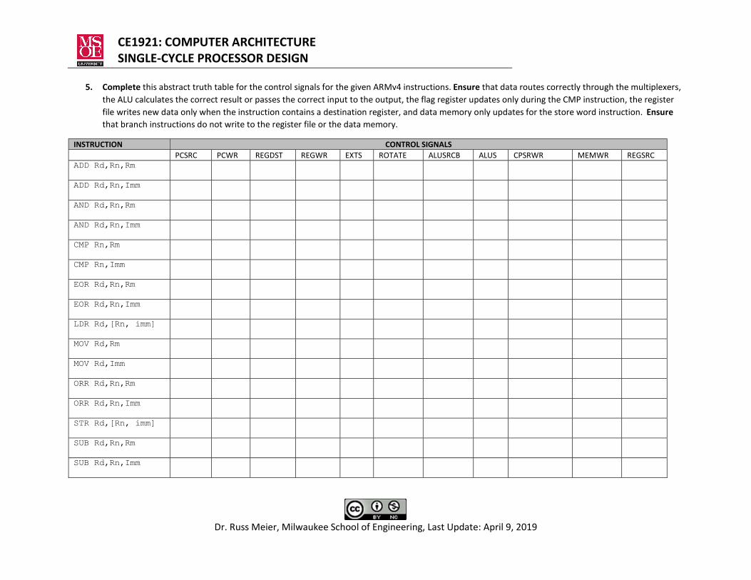
5. Complete this abstract truth table for the control signals for the given ARMv4 instructions. Ensure that data routes correctly through the multiplexers, the ALU calculates the correct result or passes the correct input to the output, the flag register updates only during the CMP instruction, the register file writes new data only when the instruction contains a destination register, and data memory only updates for the store word instruction. Ensure that branch instructions do not write to the register file or the data memory.
INSTRUCTION CONTROL SIGNALS PCSRC PCWR REGDST REGWR EXTS ROTATE ALUSRCB ALUS CPSRWR MEMWR REGSRC ADD Rd,Rn,Rm
ADD Rd,Rn,Imm
AND Rd,Rn,Rm
AND Rd,Rn,Imm
CMP Rn,Rm
CMP Rn,Imm
EOR Rd,Rn,Rm
EOR Rd,Rn,Imm
LDR Rd,[Rn, imm]
MOV Rd,Rm
MOV Rd,Imm
ORR Rd,Rn,Rm
ORR Rd,Rn,Imm
STR Rd,[Rn, imm]
SUB Rd,Rn,Rm
SUB Rd,Rn,Imm
CE1921: COMPUTER ARCHITECTURE SINGLE-CYCLE PROCESSOR DESIGN
Dr. Russ Meier, Milwaukee School of Engineering, Last Update: April 9, 2019
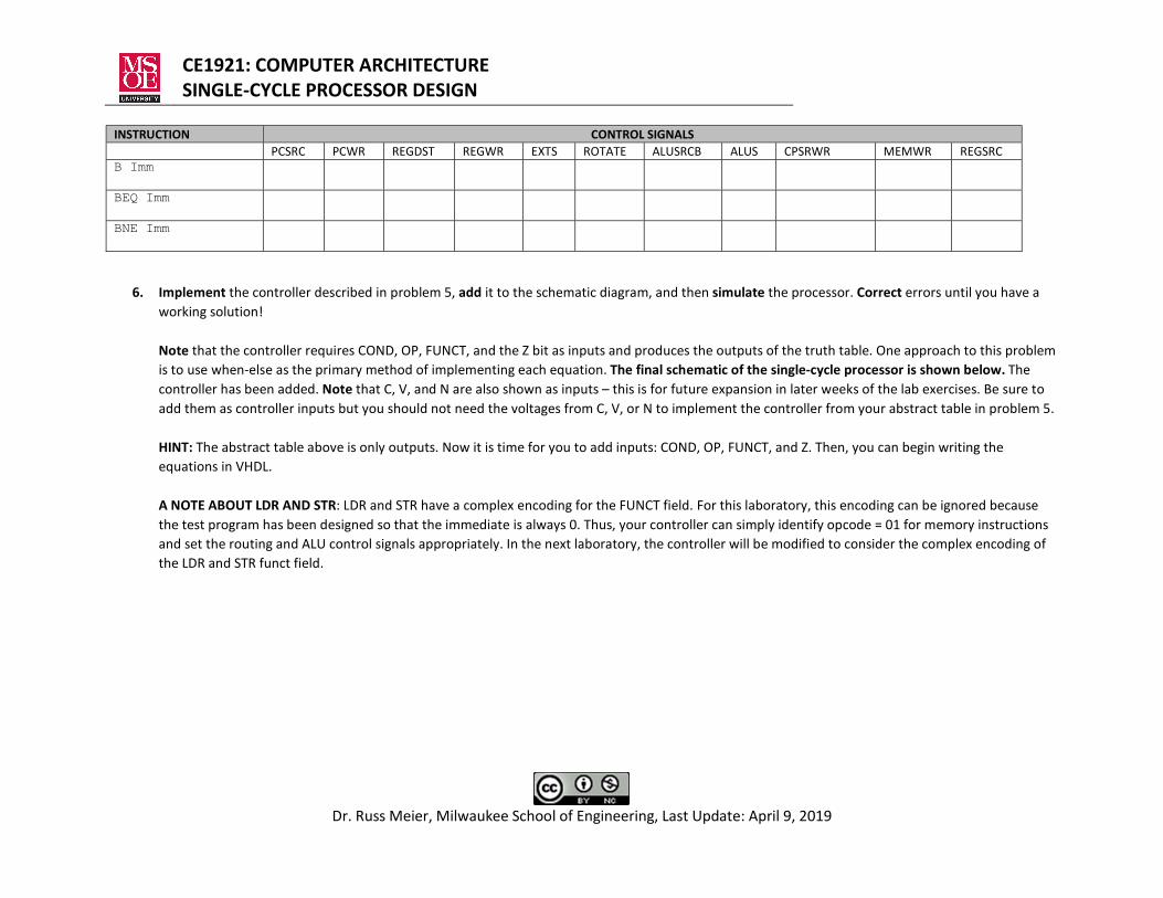
INSTRUCTION CONTROL SIGNALS PCSRC PCWR REGDST REGWR EXTS ROTATE ALUSRCB ALUS CPSRWR MEMWR REGSRC B Imm
BEQ Imm
BNE Imm
6. Implement the controller described in problem 5, add it to the schematic diagram, and then simulate the processor. Correct errors until you have a working solution! Note that the controller requires COND, OP, FUNCT, and the Z bit as inputs and produces the outputs of the truth table. One approach to this problem is to use when-else as the primary method of implementing each equation. The final schematic of the single-cycle processor is shown below. The controller has been added. Note that C, V, and N are also shown as inputs – this is for future expansion in later weeks of the lab exercises. Be sure to add them as controller inputs but you should not need the voltages from C, V, or N to implement the controller from your abstract table in problem 5. HINT: The abstract table above is only outputs. Now it is time for you to add inputs: COND, OP, FUNCT, and Z. Then, you can begin writing the equations in VHDL. A NOTE ABOUT LDR AND STR: LDR and STR have a complex encoding for the FUNCT field. For this laboratory, this encoding can be ignored because the test program has been designed so that the immediate is always 0. Thus, your controller can simply identify opcode = 01 for memory instructions and set the routing and ALU control signals appropriately. In the next laboratory, the controller will be modified to consider the complex encoding of the LDR and STR funct field.
CE1921: COMPUTER ARCHITECTURE SINGLE-CYCLE PROCESSOR DESIGN
Dr. Russ Meier, Milwaukee School of Engineering, Last Update: April 9, 2019
TOP LEVEL DESIGN
DISCUSSION
The processor begins executing the program stored in the instruction ROM after reset. One instruction executes per clock period. Simulation of the processor should set the end time so that enough clock periods allows the entire program to be visualized. Simulation of the processor should include RST, CLK, and WD3, of course, because they are the shown inputs and outputs. Good simulation will probably need additional output pins to be added so that all the control signals can be visualized, the instruction
bus can be visualized, the PC4 and BranchAddress values can be visualized, etc.
CE1921: COMPUTER ARCHITECTURE SINGLE-CYCLE PROCESSOR DESIGN
Dr. Russ Meier, Milwaukee School of Engineering, Last Update: April 9, 2019
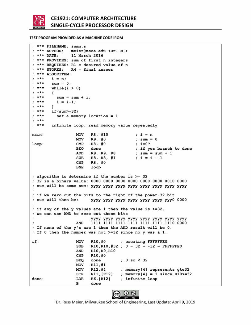
TEST PROGRAM PROVIDED AS A MACHINE CODE IROM
; *** FILENAME: sumn.s ; *** AUTHOR: [email protected] <Dr. M.> ; *** DATE: 11 March 2016 ; *** PROVIDES: sum of first n integers ; *** REQUIRES: R1 = desired value of n ; *** STORES: R4 = final answer ; *** ALGORITHM: ; *** i = n; ; *** sum = 0; ; *** while(i > 0) ; *** { ; *** sum = sum + i; ; *** i = i-1; ; *** } ; *** if(sum>=32) ; *** set a memory location = 1 ; *** ; *** infinite loop: read memory value repeatedly main: MOV R8, #10 ; i = n MOV R9, #0 ; sum = 0 loop: CMP R8, #0 ; i=0? BEQ done ; if yes branch to done ADD R9, R9, R8 ; sum = sum + i SUB R8, R8, #1 ; i = i - 1 CMP R8, #0 BNE loop ; algorithm to determine if the number is >= 32 ; 32 is a binary value: 0000 0000 0000 0000 0000 0000 0010 0000 ; sum will be some num: yyyy yyyy yyyy yyyy yyyy yyyy yyyy yyyy ; ; if we zero out the bits to the right of the power-32 bit ; sum will then be: yyyy yyyy yyyy yyyy yyyy yyyy yyy0 0000 ; ; if any of the y values are 1 then the value is >=32. ; we can use AND to zero out those bits ; yyyy yyyy yyyy yyyy yyyy yyyy yyyy yyyy ; AND 1111 1111 1111 1111 1111 1111 1110 0000 ; If none of the y's are 1 then the AND result will be 0. ; If 0 then the number was not >=32 since no y was a 1. if: MOV R10,#0 ; creating FFFFFFE0 SUB R10,R10,#32 ; 0 – 32 = -32 = FFFFFFE0 AND R10,R9,R10 CMP R10,#0 BEQ done ; 0 so < 32 MOV R11,#1 MOV R12,#4 ; memory[4] represents gte32 STR R11,[R12] ; memory[4] = 1 since R10>=32 done: LDR R6,[R12] ; infinite loop B done
CE1921: COMPUTER ARCHITECTURE SINGLE-CYCLE PROCESSOR DESIGN
Dr. Russ Meier, Milwaukee School of Engineering, Last Update: April 9, 2019
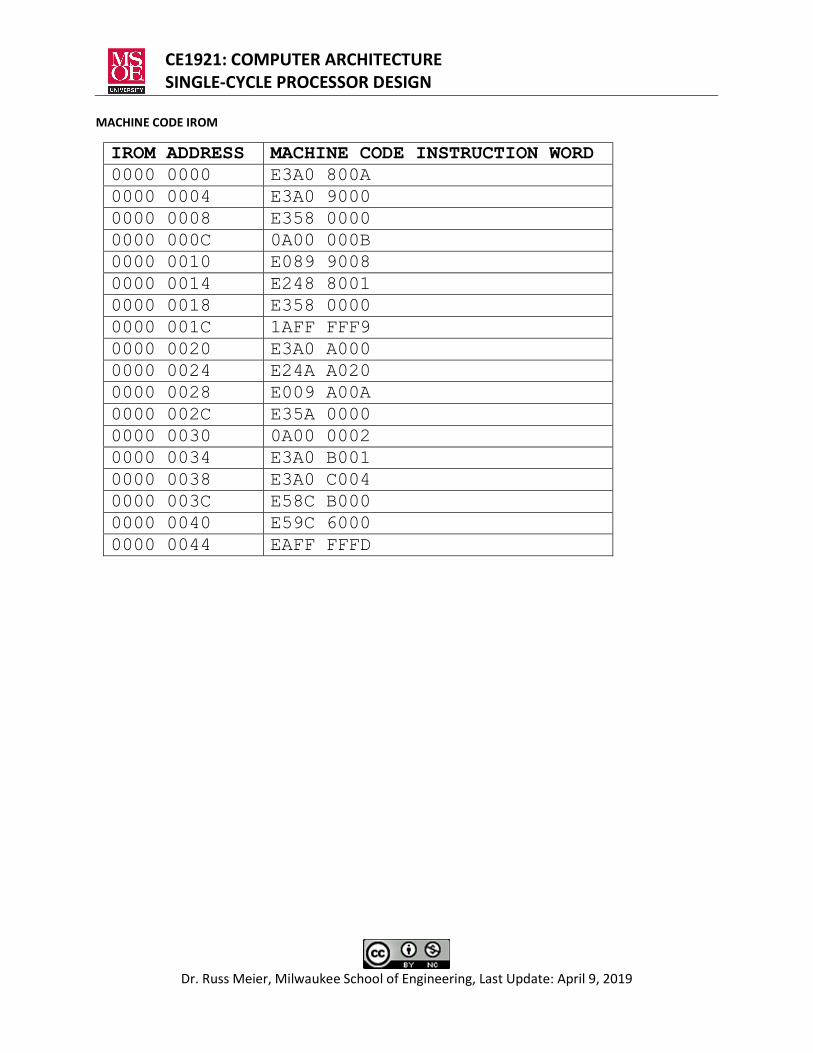
MACHINE CODE IROM
IROM ADDRESS MACHINE CODE INSTRUCTION WORD 0000 0000 E3A0 800A 0000 0004 E3A0 9000 0000 0008 E358 0000 0000 000C 0A00 000B 0000 0010 E089 9008 0000 0014 E248 8001 0000 0018 E358 0000 0000 001C 1AFF FFF9 0000 0020 E3A0 A000 0000 0024 E24A A020 0000 0028 E009 A00A 0000 002C E35A 0000 0000 0030 0A00 0002 0000 0034 E3A0 B001 0000 0038 E3A0 C004 0000 003C E58C B000 0000 0040 E59C 6000 0000 0044 EAFF FFFD


