Embed Size (px)
Citation preview
Family Name: SOLUTIONS First Name: Student ID:
Final Exam
Computer Architecture (227-2210-00L)
ETH Zürich, Fall 2020Prof. Onur Mutlu
Problem 1 (175 Points): Potpourri
Problem 2 (105 Points): DRAM Refresh
Problem 3 (90 Points): RowHammer
Problem 4 (100 Points): Processing-using-Memory
Problem 5 (70 Points): Emerging Memory Technologies
Problem 6 (100 Points): Prefetching
Problem 7 (100 Points): Cache Coherence
Problem 8 (BONUS: 90 Points): Genome Analysis
Total (740 + 90 bonus Points):
Examination Rules:
1. Written exam, 180 minutes in total.
2. No books, no calculators, no computers or communication devices. 10 single-sided (or 5 double-sided) A4pages of handwritten notes are allowed.
3. Write all your answers on this document, space is reserved for your answers after each question. Blankpages are available at the end of the exam. Do not answer questions on them.
4. Clearly indicate your final answer for each problem. Answers will only be evaluated if they are readable.
5. Put your Student ID card visible on the desk during the exam.
6. If you feel disturbed, immediately call an assistant.
7. Write with a black or blue pen (no pencil, no green, red or any other color).
8. Show all your work. For some questions, you may get partial credit even if the end result is wrong dueto a calculation mistake. If you make assumptions, state your assumptions clearly and precisely.
9. Please write your initials at the top of every page.
Tips:
• Be cognizant of time. Do not spend too much time on one question.• Be concise. You may be penalized for verbosity.• Show work when needed. You will receive partial credit at the instructors’ discretion.• Write legibly. Show your final answer.
i
Initials: Solutions Computer Architecture December 18th, 2020
This page intentionally left blank
Final Exam Page 1 of 29
Initials: Solutions Computer Architecture December 18th, 2020
1 Potpourri [175 points]
A multiple choice question can potentially have multiple correct choices. 4 incorrectly-answered ques-tions will cause you to lose 1 correctly-answered question (you can never go below 0, though, in thepoints you gain from this question). Choose wisely.
(a) [8 points] In lecture, we covered the Bloom Filter data structure. As you should recall,Bloom Filter represents set membership. Which of the following is NOT correct aboutBloom Filters?
1) It has no false negatives.
2) It has false positives.
3) It is approximate.
4) It can be used in both hardware and software.
5) In the best case, its false positive rate is 100%.
(b) [8 points] Consider the following statements about different memory technologies.Pick the one that is NOT correct.
1) DRAM is charge based memory.
2) Phase Change Memory is resistive memory.
3) Charge based memories are fundamentally less scalable than resistive memories (based on ourcurrent understanding of them).
4) Flash memory is resistive memory.
5) Both Flash memory and Phase Change Memory are non-volatile memories.
(c) [8 points] If activating row A causes some bits in row B to flip (due to RowHammer),then does activating row B cause some bits in row A to flip as well?
1) No, never.
2) Yes, always.
3) Not necessarily.
4) Only the bits that contain ‘1’ in row A will be flipped to ‘0’.
5) Only the bits that contain ‘0’ in row A will be flipped to ‘1’.
(d) [8 points] DRAM latency has improved much less than capacity or bandwidth in recentyears. The main inhibitor of DRAM latency is the long subarray bitlines. What isthe main reason manufacturers do not reduce the latency?
1) Shorter subarray bitlines result in larger chip area and higher module costs.
2) Long subarray bitlines are necessary due to the manufacturing process technology limitation.
3) Long bitlines require an extremely large sense amplifier for fast sensing. DRAM technologydoes not allow to for a faster sense amplifier structure.
4) Reducing latency requires considerable engineering effort.
5) Latency is dependent on the memory controller design, which was not redesigned in recentyears.
Final Exam Page 2 of 29
Initials: Solutions Computer Architecture December 18th, 2020
(e) [8 points] What makes it very difficult to determine the retention time of a DRAMcell?
1) Retention time of the cell can change randomly over time, due to the variable retention timephenomenon.
2) Retention time of the cell is dependent on the value stored in the cell and the cells around it.
3) The RowHammer phenomenon negatively affects the retention time of the cell.
4) Only 1) and 2).
5) 1), 2), and 3).
(f) [8 points] In lecture, we covered the idea of Heterogeneous Reliability Memory (HRM),where part of physical memory is built using very reliable DRAM chips whereas otherparts are built using unreliable DRAM chips. The system intelligently partitions thedata between the two types of memories. What is the fundamental property thatHRM relies on?
1) Even unreliable DRAM chips provide some amount of error correction.
2) Some data in a given application can tolerate the memory errors that may happen in unreliable DRAM chips.
3) The operating system can automatically detect and correct memory errors that happen inunreliable DRAM chips.
4) Only 1) and 2).
5) Only 2) and 3).
(g) [8 points] Why is a DRAM cell faster to access at low temperatures compared to athigh temperatures?
1) DRAM cell loses charge quickly at low temperatures, which causes it to be refreshed morefrequently, which, in turn, reduces the access latency of the cell.
2) DRAM cell stores more charge at low temperatures, which leads to faster sensing.
3) DRAM cell is more reliable at low temperature, which enables it to be accessed faster sincethere is less need for error correction.
4) DRAM cell is less vulnerable to RowHammer at low temperatures, making it faster to access.
5) The question starts from a wrong axiom. DRAM cell is not faster to access at low tempera-tures.
(h) [8 points] In lecture, we covered the concept of thread ranking, as a fundamentalbuilding block of modern memory controllers. The idea, as you should recall, is torank the threads based on some characteristics, and use the ranking as a prioritizationorder between requests of different threads across all banks and memory controllers.Which of the following statements is NOT correct about thread ranking?
1) Ranking a low-memory-intensity thread over a high-memory-intensity thread improves systemthroughput.
2) Ranking is complex to implement, compared to a baseline thread-unaware memory scheduler.
3) Ranking helps preserve bank-level parallelism of threads.
4) Ranking provides starvation freedom to different threads.
5) Ranking can be determined by system software, if the interfaces to the memory controller areprovided.
Final Exam Page 3 of 29
Initials: Solutions Computer Architecture December 18th, 2020
(i) [8 points] We covered the idea of the Blacklisting Memory Scheduler, which essentiallyde-prioritizes the requests of an application that has recently been serviced by thememory scheduler with a series of consecutive requests. Basically, the application getsblacklisted for a short time. The rest of the scheduling policy is similar to baselineFirst-Ready First-Come-First-Serve (FR-FCFS) policy of modern memory schedulers.Which of the following is NOT correct about the Blacklisting Memory Scheduler?
1) Blacklisting is simpler to implement than ranking of applications.
2) It adapts quickly to changing memory access behavior of different threads.
3) It explicitly tries to preserve bank-level parallelism of each thread.
4) It takes into account row buffer locality in scheduling decisions.
5) It does not take into account requests coming from accelerators with strict QoS requirements.
(j) [8 points] We discussed the idea of identifying “limiter threads” in a multithreaded ap-plication in order to prioritize them in the memory scheduler. Which of the followingcan be considered a limiter thread?
1) A thread that is holding a contended lock.
2) A thread that arrives late at a barrier synchronization point.
3) A thread that is executing a pipeline stage with the lowest throughput.
4) Only 1) and 2).
5) 1), 2), and 3).
(k) [8 points] Which of the following interference control techniques can fundamentallyreduce the load (i.e., number of outstanding requests) on the entire memory system?
1) Application-aware memory request scheduling.
2) Application-aware data mapping.
3) Application-aware source throttling.
4) Only 2) and 3).
5) 1), 2), and 3).
(l) [8 points] Assume a toy system that has 32,000,000 bytes of DRAM. Assume eachrefresh consumes 1 milliWatts (i.e., 10−3 Watts). If you are told that the total powerconsumption spent on refresh is 320 Watts, what can you conclude about the DRAMsystem?
1) The row size is 10 bytes.
2) The row size is 100 bytes.
3) The row size is 1000 bytes.
4) The row size is 10,000 bytes.
5) The row size is not possible to determine.
Final Exam Page 4 of 29
Initials: Solutions Computer Architecture December 18th, 2020
(m) [8 points] In lecture, we covered the idea of accelerating serialized code portions byshipping them to powerful cores in an asymmetric multicore system. Which of thefollowing is NOT one of the key benefits bottleneck acceleration provides in an asym-metric multicore architecture?
1) It lowers the burden on the programmer for parallel code optimization.
2) It reduces serialization due to contended locks.
3) It improves lock locality.
4) It increases the number of available parallel threads.
5) It reduces the performance impact of hard-to-parallelize code sections.
(n) [8 points] To improve the performance of a program, we decide to split the programcode into segments and run each segment on the most suitable core to run it. Whichof the following can this approach NOT achieve by itself?
1) It can accelerate segments/critical paths using specialized/heterogeneous cores.
2) It can exploit inter-segment parallelism.
3) It can improve the locality of inter-segment data.
4) It can improve the locality of within-segment data.
(o) [8 points] In a runahead execution processor, runahead mode is used to:
1) Tolerate memory latency.
2) Increase computational parallelism.
3) Increase power efficiency.
4) All of the above.
(p) [8 points] Entering runahead mode in an out-of-order runahead execution processorrequires checkpointing:
1) The store buffer.
2) The L1 instruction cache.
3) The register file.
4) All of the above.
(q) [8 points] Exiting runahead mode in an out-of-order runahead execution processorrequires:
1) Flushing the pipeline.
2) Flushing the branch predictor tables.
3) Flushing the prefetcher tables.
4) All of the above.
Final Exam Page 5 of 29
Initials: Solutions Computer Architecture December 18th, 2020
(r) [8 points] We covered the design of the Tesseract system for graph processing. Re-call that Tesseract exploits the logic layer in 3D-stacked memory to perform graphprocessing computations. Which one of the following is NOT true about Tesseract?
1) The system is programmed using message passing.
2) The system makes use of aggressive prefetching.
3) The system provides cache coherence between the CPU cores and the computation logic in the logic layer of 3D-stacked memory.
4) The system uses simple in-order cores in the logic layer of 3D-stacked memory.
5) The system exposes a very large amount of memory bandwidth to the cores.
(s) [8 points] Name the three fundamental reasons as to why the parallel portion of aparallel program is NOT perfectly parallel.
1) Synchronization overhead (e.g., updates to shared data)
2) Load imbalance overhead (imperfect parallelization)
3) Resource sharing overhead (contention among N processors)
(t) [15 points] Consider the following statement: “A sequentially consistent multiproces-sor guarantees that different executions of the same multithreaded program producethe same architecturally-exposed ordering of memory operations.”
1) Is this statement true or false? CIRCLE ONE.
1. True 2. False
2) Explain your reasoning (less than 15 words).
Sequential consistency makes no guarantees across different executions. (It is aboutthe ordering of operations within the same execution)
3) Why do we want the property described above; i.e., the property that “different executionsof the same multithreaded program produce the same architecturally-exposed ordering ofmemory operations”?
Debugging ease
Final Exam Page 6 of 29
Initials: Solutions Computer Architecture December 18th, 2020
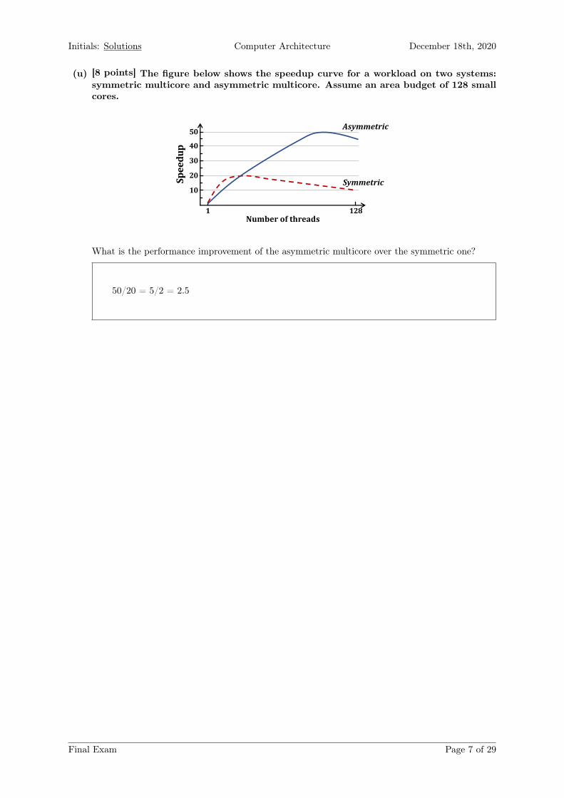
(u) [8 points] The figure below shows the speedup curve for a workload on two systems:symmetric multicore and asymmetric multicore. Assume an area budget of 128 smallcores.
Numberofthreads
Speedup
10
20
30
40
50
1 128
Asymmetric
Symmetric
What is the performance improvement of the asymmetric multicore over the symmetric one?
50/20 = 5/2 = 2.5
Final Exam Page 7 of 29
Initials: Solutions Computer Architecture December 18th, 2020
2 DRAM Refresh [105 points]
2.1 Basics [30 points]
A memory system is composed of eight banks, and each bank contains 216 rows. Every DRAM rowrefresh is initiated by a command from the memory controller, and it refreshes a single row in a singleDRAM bank. Each refresh command keeps the command bus busy for 5 ns. We define command busutilization as the fraction of total execution time during which the command bus is occupied.
1. [10 points] Given that the refresh interval is 64ms, calculate the command bus utilization of refreshcommands. Show your work step-by-step.
Command bus is utilized for 8× 216 × 5ns at every 64ms.Utilization = (219 × 5ns)/(26 × 106ns) = 213/(2× 105) = 212 × 10−5 = 4.096%
2. [20 points] Now assume 60% of all rows can withstand a refresh interval of 128 ms. If we areable to customize the refresh rate of each row independently, up to how much could we reduce thecommand bus utilization of refresh commands? Calculate the reduction (1− new
old ) in bus utilization.Show your work step-by-step.
At every 128ms:• 60% of the rows are refreshed once.Command bus is busy for: 0.6× 8× 216 × 5ns = 3× 219ns
• 40% of the rows are refreshed two times.Command bus is busy for: 0.4× 8× 216 × 5ns× 2 = 4× 219ns
Utilization = (3 + 4)× 219ns/128ms = 7× 212 × 10−6
Reduction = 1− (0.7× 212 × 10−5)/(212 × 10−5) = 30%
2.2 VRL: Variable Refresh Latency [75 points]
In this question, you are asked to evaluate "Variable Refresh Latency," proposed by Das et al. in DAC2018.1
The paper presents two key observations:
• First, a cell’s charge reaches 95% of the maximum charge level in 60% of the nominal latency valueduring a refresh operation. In other words, the last 40% of the refresh latency is spent to increasethe charge of a cell from 95% to 100%. Based on this observation, the paper defines two types ofrefresh operations: (1) full refresh and (2) partial refresh. Full refresh uses the nominal latencyvalue and restores the cell charge to 100%, while the latency of partial refresh is only 60% of thenominal latency value and it restores 95% of the charge.
1Das, A. et al., "VRL-DRAM: Improving DRAM Performance via Variable Refresh Latency." In Proceedings of the55th Annual Design Automation Conference (DAC), 2018.
Final Exam Page 8 of 29
Initials: Solutions Computer Architecture December 18th, 2020
• Second, a fully refreshed cell operates correctly even after multiple partial refreshes, but it needs tobe fully refreshed again after a finite number of partial refreshes. The maximum number of partialrefreshes before a full refresh is required varies from cell to cell.
The key idea of the paper is to apply a full refresh operation only when necessary and use partial re-fresh operations at all other times.
(a) [25 points] Consider a case in which:
• Each row must be refreshed every 64 ms. In other words, the refresh interval is 64 ms.
• Row refresh commands are evenly distributed across the refresh interval. In other words, allrows are refreshed exactly once in any given 64 ms time window.
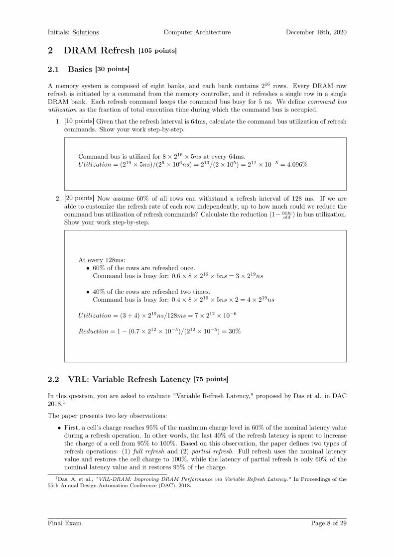
• You are given the following plot, which shows the distribution of the maximum number ofpartial refreshes across all rows of a particular bank. For example, if the maximum numberof refreshes is three, those rows can be partially refreshed for at most three refresh intervals,and the fourth refresh operation must be a full refresh.
• If all rows were always fully refreshed, the time that a bank is busy serving the refresh requestswithin a refresh interval would be T.
10
20
30
40
0 10 20 30 40 50
0
1
3
7
15
Fraction of Rows (%)
Max
Num
ber
of P
artia
l Ref
resh
es
Refresh interval: 64ms
10
2010
20
40
0 10 20 30 40 50
0
1
3
7
15
Fraction of Rows (%)
Max
Num
ber
of P
artia
l Ref
resh
es
Refresh interval: 128ms
How much time does it take (in terms of T) for a bank to refresh all rows within a refresh interval,after applying Variable Refresh Latency?
Full refresh latency = T, partial refresh latency = 0.6T.
10% of the rows are fully refreshed at every other interval:0.1× (1/2× 0.6T + 1/2× T )20% of the rows are fully refreshed after every three partial refresh:0.2× (3/4× 0.6T + 1/4× T )30% of the rows are fully refreshed after every seven partial refresh:0.3× (7/8× 0.6T + 1/8× T )40% of the rows are fully refreshed after every fifteen partial refresh:0.4× (15/16× 0.6T + 1/16× T )
Then, new refresh latency of a bank would be 0.665T.
Final Exam Page 9 of 29
Initials: Solutions Computer Architecture December 18th, 2020
(b) [25 points] You find out that you can relax the refresh interval, and define your baseline as follows:
• 75% of the rows are refreshed at every 128ms; 25% of the rows are refreshed at every 64ms.
• Refresh commands are evenly distributed in time.
• All rows are always fully refreshed.
• A single refresh command costs 0.2/N ms, where N is the number of rows in a bank.
• Refresh overhead is defined as the fraction of time that a bank is busy, serving the refreshrequests over a very large period of time.
Calculate the refresh overhead for the baseline.
At every 128ms:
25% of the rows are refreshed twice, 75% of the rows are refreshed once.
Total time spent for refresh in a 128 ms. interval is (0.75N+2×0.25N)×0.2/N = 0.25ms.
Then refresh overhead is 0.25/128
Final Exam Page 10 of 29
Initials: Solutions Computer Architecture December 18th, 2020
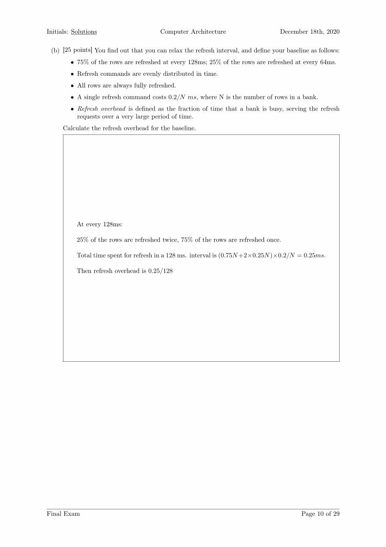
(c) [25 points] Consider a case where:
• 90% of the rows are refreshed at every 128ms; 10% of the rows are refreshed at every 64ms.
• Refresh commands are evenly distributed in time.
• You are given the following plot, which shows the distribution of the maximum number ofpartial refreshes across all rows of a particular bank.
• A single refresh command costs 0.2/N ms, where N is the number of rows in a bank.
• Refresh overhead is defined as the fraction of time that a bank is busy, serving the refreshrequests over a very large period of time.
1020
30
40
0 10 20 30 40 50
0
1
3
7
15
Fraction of Rows (%)
Max
Num
ber
of P
artia
l Ref
resh
es
Refresh interval: 128msRefresh interval: 64ms
Calculate the refresh overhead. Show your work step-by-step. Then, compare it against the baselineconfiguration (part b). How much reduction (1− new
old ) do you see in the performance overhead ofrefreshes?
Full refresh of a row costs 0.2/N ms. Then, partial refresh of a row costs 0.12/N ms
At every 8× 128 ms:• 10% of the rows are refreshed 16 times:8 times fully refreshed and 8 times partially refreshed.
• 20% of the rows are refreshed 8 times:4 times fully refreshed and 4 times partially refreshed.
• 30% of the rows are refreshed 8 times:2 times fully refreshed and 6 times partially refreshed.
• 40% of the rows are refreshed 8 times:1 time fully refreshed and 7 times partially refreshed.
The Total time spent for refresh is:= (0.1N × 8 + 0.2N × 4 + 0.3N × 2 + 0.4N × 1)× 0.2/N+ (0.1× 8 + 0.2N × 4 + 0.3N × 6 + 0.4N × 7)× 0.12/N
= (0.8 + 0.8 + 0.6 + 0.4)× 0.2 + (0.8 + 0.8 + 1.8 + 2.8)× 0.12= 0.52 + 0.744 = 1.264msThen, refresh overhead is 1.264/(8× 128)So, the reduction is 1− (1.264/8)/0.25 ≈ 36.8%.
Final Exam Page 11 of 29
Initials: Solutions Computer Architecture December 18th, 2020
3 RowHammer [90 points]
3.1 RowHammer Properties [15 points]
Determine whether each of the following statements is true or false. Note: we will subtract 1.5 pointsfor each incorrect answer. (The minimum score you can get for this question is 0 point.)
(a) [3 points] Violating DRAM timing parameters is necessary to induce RowHammer bit flips.
1. True 2. False
(b) [3 points] SECDED (Single Error Correction Double Error Detection) Hamming ECC cannot guar-antee RowHammer-safe operation.
1. True 2. False
(c) [3 points] Mobile devices are RowHammer-safe because they use low power memory chips.
1. True 2. False
(d) [3 points] We can more effectively induce bit flips in a given victim row by hammering rows indifferent banks.
1. True 2. False
(e) [3 points] In DRAM TRR (Target Row Refresh) mechanism provides RowHammer-safe operation.The only problem is that it is not implemented in all DRAM chips.
1. True 2. False
3.2 RowHammer Mitigation [75 points]
You are assigned to implement a RowHammer mitigation mechanism within the memory controller of anew processor. The DRAM chips that will be used with the processor are organized as 1 channel, 1 rank,8 banks, 8 KB row size, and 1 GB total capacity. The DRAM protocol specifies that each row shouldbe refreshed every 64 ms, and there should be at least 64 ns between two row activations targeting thesame DRAM bank. The RowHammer threshold of the chips is 50,000 row activations per aggressor rowduring a double-sided attack, while no hammer count for a single-sided attack can induce bit flips within64 ms.
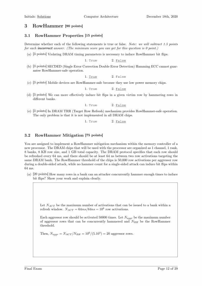
(a) [20 points] How many rows in a bank can an attacker concurrently hammer enough times to inducebit flips? Show your work and explain clearly.
Let NACT be the maximum number of activations that can be issued to a bank within arefresh window. NACT = 64ms/64ns = 106 row activations.
Each aggressor row should be activated 50000 times. Let Naggr be the maximum numberof aggressor rows that can be concurrently hammered and NRH be the RowHammerthreshold.
Then, Naggr = NACT /NRH = 106/(5.104) = 20 aggressor rows.
Final Exam Page 12 of 29
Initials: Solutions Computer Architecture December 18th, 2020
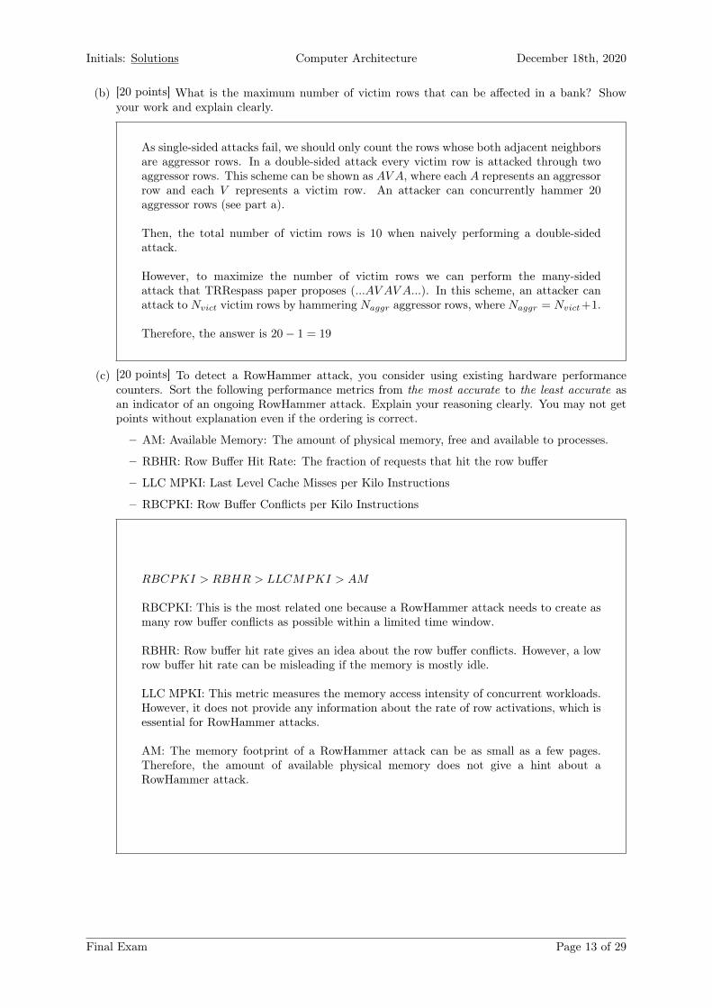
(b) [20 points] What is the maximum number of victim rows that can be affected in a bank? Showyour work and explain clearly.
As single-sided attacks fail, we should only count the rows whose both adjacent neighborsare aggressor rows. In a double-sided attack every victim row is attacked through twoaggressor rows. This scheme can be shown as AV A, where each A represents an aggressorrow and each V represents a victim row. An attacker can concurrently hammer 20aggressor rows (see part a).
Then, the total number of victim rows is 10 when naively performing a double-sidedattack.
However, to maximize the number of victim rows we can perform the many-sidedattack that TRRespass paper proposes (...AV AV A...). In this scheme, an attacker canattack to Nvict victim rows by hammering Naggr aggressor rows, where Naggr = Nvict+1.
Therefore, the answer is 20− 1 = 19
(c) [20 points] To detect a RowHammer attack, you consider using existing hardware performancecounters. Sort the following performance metrics from the most accurate to the least accurate asan indicator of an ongoing RowHammer attack. Explain your reasoning clearly. You may not getpoints without explanation even if the ordering is correct.
– AM: Available Memory: The amount of physical memory, free and available to processes.
– RBHR: Row Buffer Hit Rate: The fraction of requests that hit the row buffer
– LLC MPKI: Last Level Cache Misses per Kilo Instructions
– RBCPKI: Row Buffer Conflicts per Kilo Instructions
RBCPKI > RBHR > LLCMPKI > AM
RBCPKI: This is the most related one because a RowHammer attack needs to create asmany row buffer conflicts as possible within a limited time window.
RBHR: Row buffer hit rate gives an idea about the row buffer conflicts. However, a lowrow buffer hit rate can be misleading if the memory is mostly idle.
LLC MPKI: This metric measures the memory access intensity of concurrent workloads.However, it does not provide any information about the rate of row activations, which isessential for RowHammer attacks.
AM: The memory footprint of a RowHammer attack can be as small as a few pages.Therefore, the amount of available physical memory does not give a hint about aRowHammer attack.
Final Exam Page 13 of 29
Initials: Solutions Computer Architecture December 18th, 2020
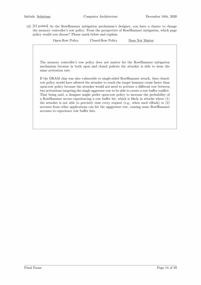
(d) [15 points] As the RowHammer mitigation mechanism’s designer, you have a chance to changethe memory controller’s row policy. From the perspective of RowHammer mitigation, which pagepolicy would you choose? Please mark below and explain.
Open-Row Policy Closed-Row Policy Does Not Matter
The memory controller’s row policy does not matter for the RowHammer mitigationmechanism because in both open and closed policies the attacker is able to issue thesame activation rate.
If the DRAM chip was also vulnerable to single-sided RowHammer attack, then closed-row policy would have allowed the attacker to reach the target hammer count faster thanopen-row policy because the attacker would not need to activate a different row betweentwo activations targeting the single aggressor row to be able to create a row buffer conflict.That being said, a designer might prefer open-row policy to increase the probability ofa RowHammer access experiencing a row buffer hit, which is likely in attacks where (1)the attacker is not able to precisely time every request (e.g., when used clflush) or (2)accesses from other applications can hit the agggressor row, causing some RowHammeraccesses to experience row buffer hits.
Final Exam Page 14 of 29
Initials: Solutions Computer Architecture December 18th, 2020
4 Processing-using-Memory [100 points]
One promising trend in the Processing-in-Memory paradigm is Processing-using-Memory (PuM), whichexploits the analog operation of memory cells to execute bulk bitwise operations. A pioneering proposalin PuM in DRAM technology is Ambit, which we discussed in class. Ambit provides the ability toperform bitwise AND/OR of two rows in a subarray and NOT of one row. Since Ambit is logicallycomplete, it is possible to implement any other logic gate (e.g., XOR). However, to be able to implementarithmetic operations (e.g., addition), bit shifting is also necessary. There is no way of shifting bits inDRAM with a conventional layout, but there are two possible approaches to modifying DRAM to enablebit shifting.
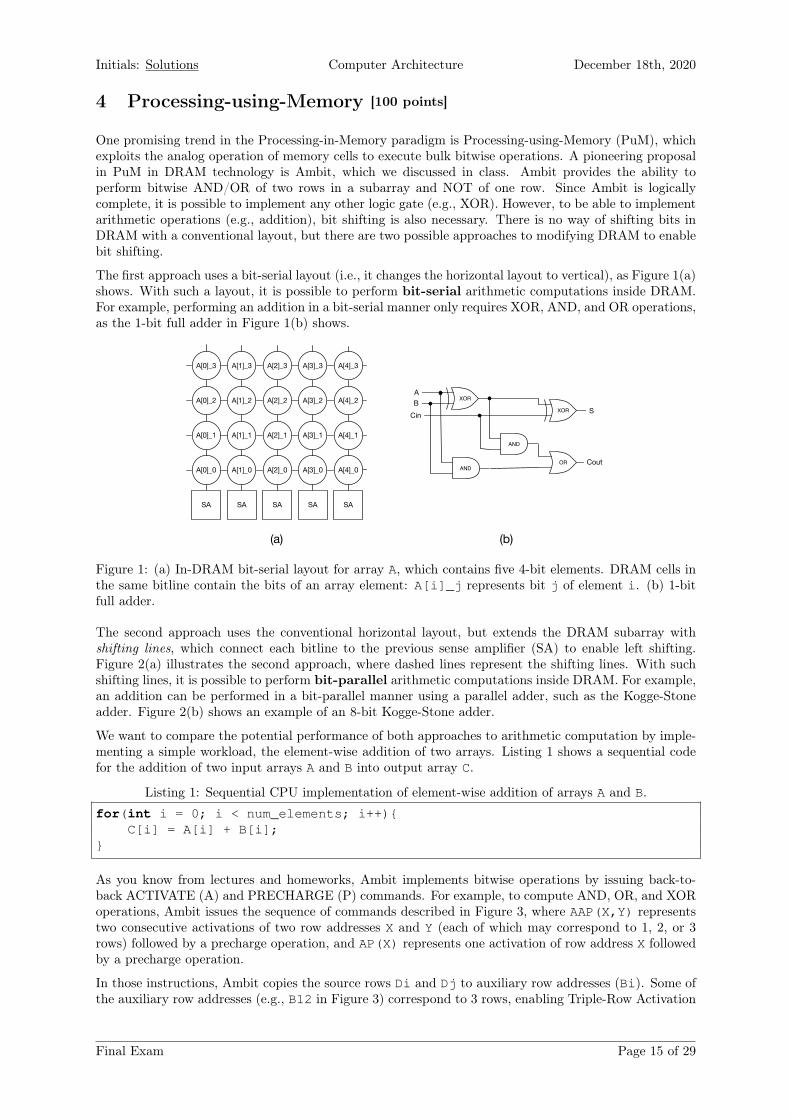
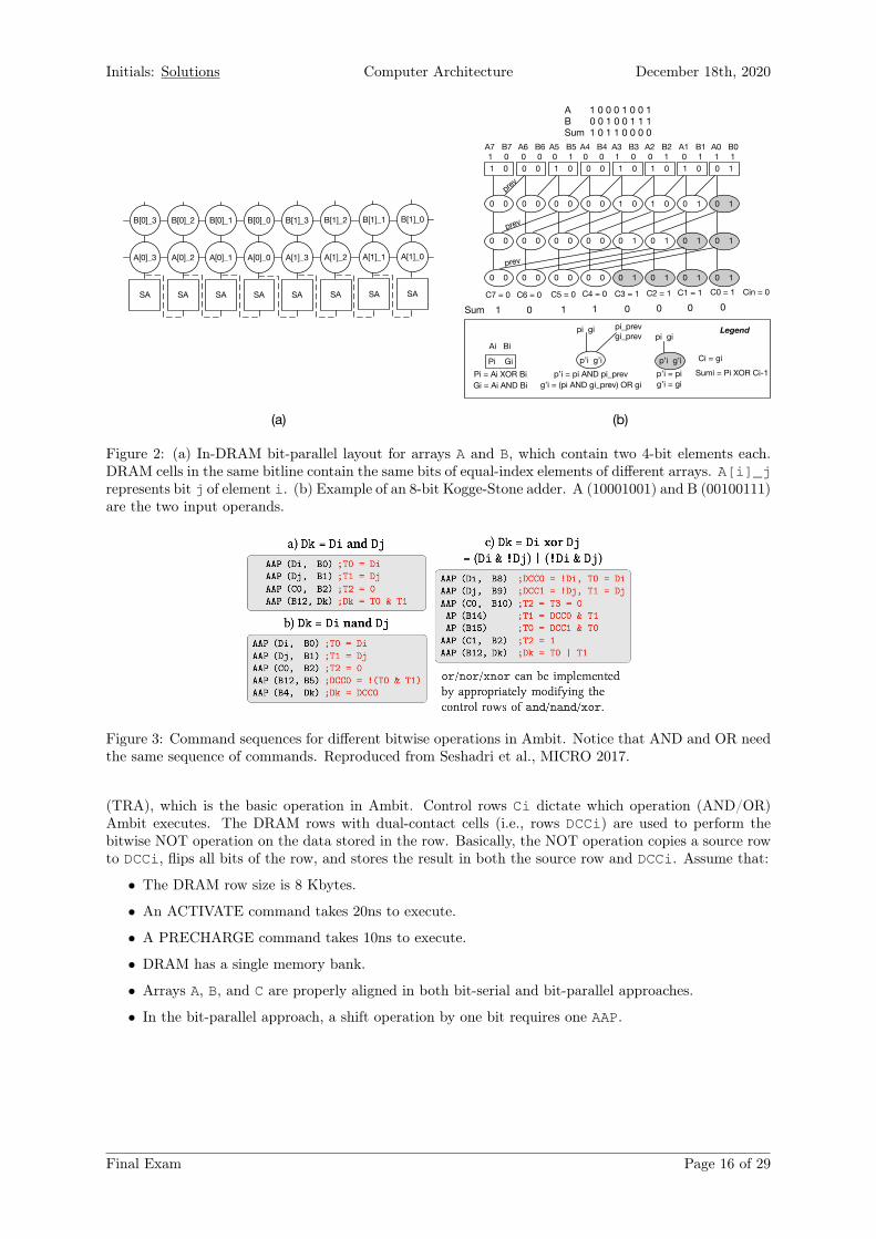
The first approach uses a bit-serial layout (i.e., it changes the horizontal layout to vertical), as Figure 1(a)shows. With such a layout, it is possible to perform bit-serial arithmetic computations inside DRAM.For example, performing an addition in a bit-serial manner only requires XOR, AND, and OR operations,as the 1-bit full adder in Figure 1(b) shows.
A[0]_3
A[0]_2
A[0]_1
A[0]_0
A[1]_3
A[1]_2
A[1]_1
A[1]_0
A[2]_3
A[2]_2
A[2]_1
A[2]_0
A[3]_3
A[3]_2
A[3]_1
A[3]_0
A[4]_3
A[4]_2
A[4]_1
A[4]_0
SA SA SA SA SA
XOR
XOR
AND
AND
OR
ABCin S
Cout
(a) (b)
Figure 1: (a) In-DRAM bit-serial layout for array A, which contains five 4-bit elements. DRAM cells inthe same bitline contain the bits of an array element: A[i]_j represents bit j of element i. (b) 1-bitfull adder.
The second approach uses the conventional horizontal layout, but extends the DRAM subarray withshifting lines, which connect each bitline to the previous sense amplifier (SA) to enable left shifting.Figure 2(a) illustrates the second approach, where dashed lines represent the shifting lines. With suchshifting lines, it is possible to perform bit-parallel arithmetic computations inside DRAM. For example,an addition can be performed in a bit-parallel manner using a parallel adder, such as the Kogge-Stoneadder. Figure 2(b) shows an example of an 8-bit Kogge-Stone adder.
We want to compare the potential performance of both approaches to arithmetic computation by imple-menting a simple workload, the element-wise addition of two arrays. Listing 1 shows a sequential codefor the addition of two input arrays A and B into output array C.
Listing 1: Sequential CPU implementation of element-wise addition of arrays A and B.
for(int i = 0; i < num_elements; i++){C[i] = A[i] + B[i];
}
As you know from lectures and homeworks, Ambit implements bitwise operations by issuing back-to-back ACTIVATE (A) and PRECHARGE (P) commands. For example, to compute AND, OR, and XORoperations, Ambit issues the sequence of commands described in Figure 3, where AAP(X,Y) representstwo consecutive activations of two row addresses X and Y (each of which may correspond to 1, 2, or 3rows) followed by a precharge operation, and AP(X) represents one activation of row address X followedby a precharge operation.
In those instructions, Ambit copies the source rows Di and Dj to auxiliary row addresses (Bi). Some ofthe auxiliary row addresses (e.g., B12 in Figure 3) correspond to 3 rows, enabling Triple-Row Activation
Final Exam Page 15 of 29
Initials: Solutions Computer Architecture December 18th, 2020
B[0]_3
A[0]_3
B[0]_2
A[0]_2
B[0]_1
A[0]_1
B[0]_0
A[0]_0
B[1]_3
A[1]_3
SA SA SA SA SA
B[1]_2
A[1]_2
SA
B[1]_1
A[1]_1
SA
B[1]_0
A[1]_0
SA
1 0 0 0 1 0 0 0 1 0 1 0 1 0 0 1
0 0 0 0 0 0 0 0 1 0 1 0 0 1 0 1
0 0 0 0 0 0 0 0 0 1 0 1 0 1 0 1
0 0 0 0 0 0 0 0 0 1 0 1 0 1 0 1
C7 = 0 C6 = 0 C5 = 0 C4 = 0 C3 = 1 C2 = 1 C1 = 1 C0 = 1 Cin = 0
1 0 1 1 0 0 0 0
prev
prev
prev
A 1 0 0 0 1 0 0 1B 0 0 1 0 0 1 1 1Sum 1 0 1 1 0 0 0 0
A7 B71 0
A6 B60 0
A5 B50 1
A4 B40 0
A3 B31 0
A2 B20 1
A1 B10 1
A0 B01 1
Pi GiPi = Ai XOR BiGi = Ai AND Bi
Ai Bip’i g’i
p’i = pi AND pi_prevg’i = (pi AND gi_prev) OR gi
p’i g’i
pi gi
p’i = pig’i = gi
pi gi pi_prevgi_prev
Ci = giSumi = Pi XOR Ci-1
Sum
Legend
(a) (b)
Figure 2: (a) In-DRAM bit-parallel layout for arrays A and B, which contain two 4-bit elements each.DRAM cells in the same bitline contain the same bits of equal-index elements of different arrays. A[i]_jrepresents bit j of element i. (b) Example of an 8-bit Kogge-Stone adder. A (10001001) and B (00100111)are the two input operands.
Figure 3: Command sequences for different bitwise operations in Ambit. Notice that AND and OR needthe same sequence of commands. Reproduced from Seshadri et al., MICRO 2017.
(TRA), which is the basic operation in Ambit. Control rows Ci dictate which operation (AND/OR)Ambit executes. The DRAM rows with dual-contact cells (i.e., rows DCCi) are used to perform thebitwise NOT operation on the data stored in the row. Basically, the NOT operation copies a source rowto DCCi, flips all bits of the row, and stores the result in both the source row and DCCi. Assume that:
• The DRAM row size is 8 Kbytes.
• An ACTIVATE command takes 20ns to execute.
• A PRECHARGE command takes 10ns to execute.
• DRAM has a single memory bank.
• Arrays A, B, and C are properly aligned in both bit-serial and bit-parallel approaches.
• In the bit-parallel approach, a shift operation by one bit requires one AAP.
Final Exam Page 16 of 29
Initials: Solutions Computer Architecture December 18th, 2020
(a) [40 points] Compute the maximum throughput in terms of addition operations per second (OPS)of the bit-serial approach as a function of the element size (i.e., bits/element).
Throughputbit−serial =65,5361220×nGOPS.
Explanation:Since DRAM has one single bank (and we can operate on a single subarray), themaximum throughput is achieved when we use complete rows. As the row size is 8KB,the maximum array size that we can work with is 65,536 elements.
First, we obtain the execution time as a function of the number of bits per element.Each XOR operation employs 12 ACTIVATION and 7 PRECHARGE operations. ForAND and OR, 8 ACTIVATION and 4 PRECHARGE operations. Thus, the executiontime of the bit-serial computation on one DRAM subarray can be computed as (n is thenumber of bits per element):tbit−serial = (2× tXOR + 2× tAND + tOR)× n;tbit−serial = 1220× n ns.
Second, we obtain the throughput in arithmetic operations per second (OPS) as:Throughputbit−serial =
65,5361220×n×10−9 = 65,536
1220×nGOPS.
(b) [35 points] Compute the maximum throughput in terms of addition operations per second (OPS)of the bit-parallel approach as a function of the element size (i.e., bits/element). Hint:
∑ni=0 x
i =1−xn+1
1−x .
Throughputbit−parallel =65,536
(820+log n×(500+100×n))×10−9×nGOPS.
Explanation:This approach requires log n iterations. Before the first iteration (iteration 0), one XORand one AND are executed. After the last iteration (iteration (log n) − 1), one XORis executed. In each iteration, two AND and one OR are executed. It is also necessaryto shift pi_prev and gi_prev by an amount that depends on the iteration number: initeration 0, we shift 1 bit; in iteration 1, 2 bits; in iteration 2, 4 bits... Thus, the shiftamount is 2i, where i is the iteration number.First, we obtain the execution time as a function of the number of bits per element(n). The execution time of the bit-parallel computation on one DRAM subarray can becomputed as:tbit−parallel = (2×tXOR)+tAND+ log n× [2×tAND+tOR+
∑(log n)−1i=0 (2i×2×tSHIFT )];
tbit−parallel = 820 + log n× (600 + 100× (n− 1)) = 820 + log n× (500 + 100× n) ns.
Second, we obtain the throughput in arithmetic operations per second (OPS). We shouldtake into account that the number of elements per DRAM row is also a function of n,i.e., 65,536
n :Throughputbit−parallel = 65,536/n
(820+log n×(500+100×n))×10−9 =65,536
(820+log n×(500+100×n))×10−9×nGOPS.
Final Exam Page 17 of 29
Initials: Solutions Computer Architecture December 18th, 2020
(c) [25 points] Determine the element size (in bits) for which one approach (i.e., bit-serial or bit-parallel) is preferred over the other one.
There is no number of bits per element (greater than 1) that makes the bit-parallelapproach faster than the bit-serial approach.
Explanation:We want to find n such that Throughputbit−serial < Throughputbit−parallel. If we useconsider one DRAM subarray:Throughputbit−serial < Throughputbit−parallel;65,5361220×n < 65,536
(820+log n×(500+100×n))×n ; 1220 > 820+ log n× (500+ 100×n); 400 > log n×(500 + 100× n);There is no n greater than 1 that makes the bit-parallel implementation higher through-put than the bit-serial implementation.
Final Exam Page 18 of 29
Initials: Solutions Computer Architecture December 18th, 2020
5 Emerging Memory Technologies [70 points]
5.1 Phase Change Memory [15 points]
Indicate whether each of the following statements is true or false. Note: we will subtract 1.5 points foreach incorrect answer. (The minimum score you can get for this question is 0 point.)
(a) [3 points] Phase Change Memory (PCM) is more technology-scalable than DRAM.
1. True 2. False
(b) [3 points] PCM read/write operations are more energy efficient than DRAM read/write operations.
1. True 2. False
(c) [3 points] PCM provides shorter access latency but has lower endurance compared to NAND flashmemory.
1. True 2. False
(d) [3 points] Row-buffer hit latencies of DRAM and PCM are comparable.
1. True 2. False
(e) [3 points] Row-buffer miss penalty is smaller in PCM than in DRAM, since PCM commonly employsa small row buffer.
1. True 2. False
5.2 SAFARI-RAM [55 points]
Researchers in the SAFARI Research Group developed a new non-volatile memory technology, SAFARI-RAM. The read and write latency of SAFARI-RAM is close to that of DRAM while providing highermemory density compared to the latest DRAM technologies. However, SAFARI-RAM has one shortcom-ing: it has limited endurance, i.e., a memory cell fails after 107 writes are performed to the cell (knownas cell wear-out).
A bright ETH student has built a computer system using SAFARI-RAM as the main memory. SAFARI-RAM exploits a perfect wear-leveling mechanism, i.e., a mechanism that equally distributes the writesacross all of the cells of the main memory.
The student wants to estimate the worst-case lifetime of SAFARI-RAM when used as main memory.The student executes a test program to wear out the entire SAFARI-RAM as quickly as possible. Thetest program runs special instructions to bypass the cache hierarchy and repeatedly writes data intodifferent pages until all the SAFARI-RAM cells are worn out. The student’s measurements show thatSAFARI-RAM stops functioning (i.e., all its cells are worn-out) in 2.5 years. Assume the following:
• The processor is in-order.
• There is no memory-level parallelism (i.e., there is a single bank in the memory system).
• It takes 32 ns to send a memory request from the processor to the memory controller.
• It takes 52 ns to send the request from the memory controller to SAFARI-RAM.
• The write latency of SAFARI-RAM is 172 ns.
• Each write request is fully serialized, i.e., there are three steps of write requests: (1) memoryrequest from CPU to controller, (2) write request from controller to SAFARI-RAM, and (3) datawrite to SAFARI-RAM cells. None of the steps can be pipelined.
• SAFARI-RAM requests are issued at page granularity, where the page size is 4,096 bytes (4 KiB).
• SAFARI-RAM adopts a quad-level cell (QLC) technique that stores four bits in a single memorycell.
Final Exam Page 19 of 29
Initials: Solutions Computer Architecture December 18th, 2020
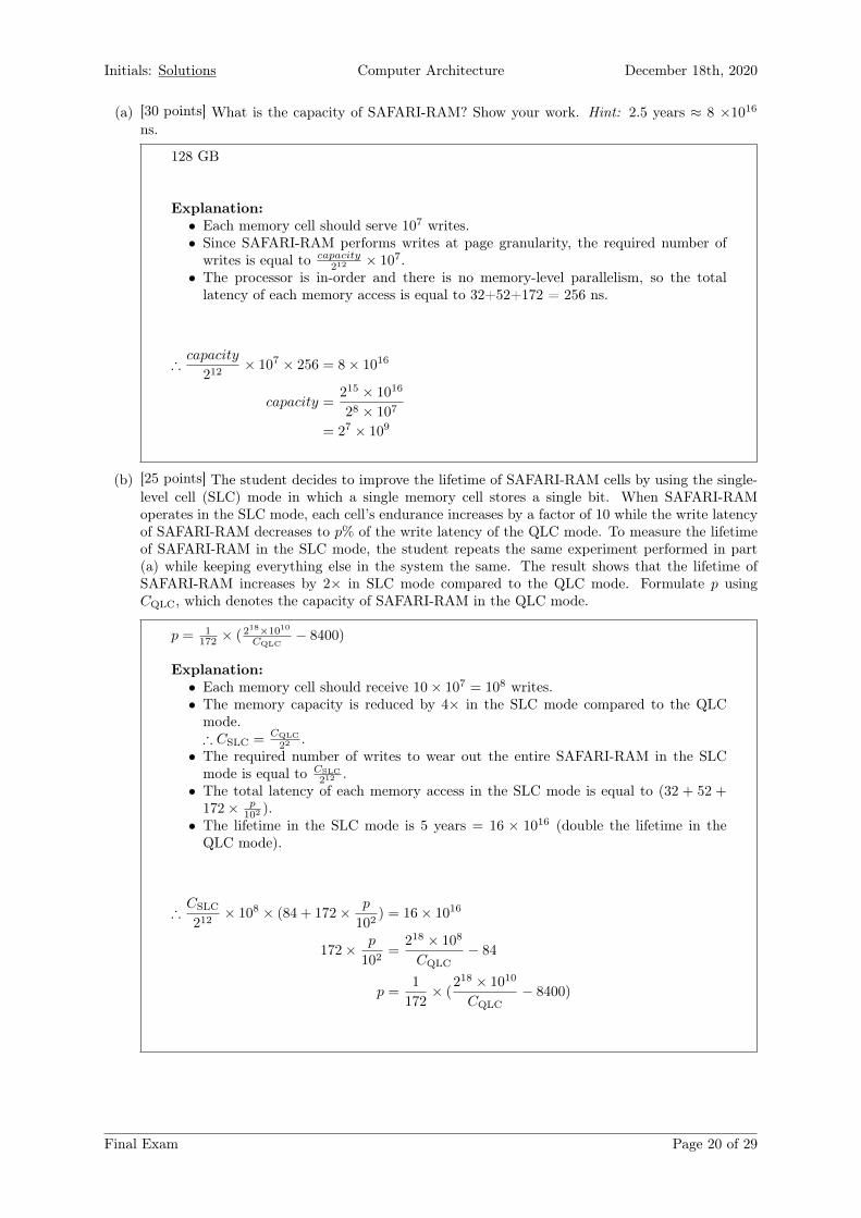
(a) [30 points] What is the capacity of SAFARI-RAM? Show your work. Hint: 2.5 years ≈ 8 ×10¹⁶ns.
128 GB
Explanation:• Each memory cell should serve 107 writes.• Since SAFARI-RAM performs writes at page granularity, the required number ofwrites is equal to capacity
212 × 107.• The processor is in-order and there is no memory-level parallelism, so the totallatency of each memory access is equal to 32+52+172 = 256 ns.
∴capacity
212× 107 × 256 = 8× 10¹⁶
capacity =215 × 1016
28 × 107
= 27 × 109
(b) [25 points] The student decides to improve the lifetime of SAFARI-RAM cells by using the single-level cell (SLC) mode in which a single memory cell stores a single bit. When SAFARI-RAMoperates in the SLC mode, each cell’s endurance increases by a factor of 10 while the write latencyof SAFARI-RAM decreases to p% of the write latency of the QLC mode. To measure the lifetimeof SAFARI-RAM in the SLC mode, the student repeats the same experiment performed in part(a) while keeping everything else in the system the same. The result shows that the lifetime ofSAFARI-RAM increases by 2× in SLC mode compared to the QLC mode. Formulate p usingCQLC, which denotes the capacity of SAFARI-RAM in the QLC mode.
p = 1172 × ( 2
18×1010
CQLC− 8400)
Explanation:• Each memory cell should receive 10× 107 = 108 writes.• The memory capacity is reduced by 4× in the SLC mode compared to the QLCmode.∴ CSLC =
CQLC22 .
• The required number of writes to wear out the entire SAFARI-RAM in the SLCmode is equal to CSLC
212 .• The total latency of each memory access in the SLC mode is equal to (32 + 52 +172× p
102 ).• The lifetime in the SLC mode is 5 years = 16 × 1016 (double the lifetime in the
QLC mode).
∴CSLC
212× 108 × (84 + 172× p
102) = 16× 1016
172× p
102=
218 × 108
CQLC− 84
p =1
172× (
218 × 1010
CQLC− 8400)
Final Exam Page 20 of 29
Initials: Solutions Computer Architecture December 18th, 2020
6 Prefetching [100 points]
A processor is observed to have the following access pattern to cache blocks. Note that the addressesare cache block addresses, not byte addresses. This pattern is repeated for a large number of iterations.
Access Pattern P : A, A+ 3, A+ 6, A, A+ 5
Each cache block is 8 KB. The hardware has a fully associative cache with LRU replacement policy anda total size of 24 KB.
None of the prefetchers mentioned in this problem employ confidence bits, but they all start out withempty tables at the beginning of the access stream shown above. Unless otherwise stated, assume that 1)each access is separated long enough in time such that all prefetches issued can complete before the nextaccess happens, and 2) the prefetchers have large enough resources to detect and store access patterns.
(a) [20 points] You have a stream prefetcher (i.e., a next-N -block prefetcher), but you do not knowthe prefetch degree (N) of it. However, you have a magical tool that displays the coverage andaccuracy of the prefetcher. When you run a large number of repetitions of access pattern P, youget 40% coverage and 10% accuracy. What is the degree of this prefetcher (i.e., N)?
Next 4 blocks.
40% coverage with a stream prefetcher for this pattern means blocks A+3 and A+6 areprefetched. Possible N at this point are 3 and 4. Accuracy 10% = 2/(N ∗ 5), so N is 4.
(b) [20 points] You are not satisfied with the performance of the stream prefetcher, so you decide toswitch to a PC-based stride prefetcher that issues prefetch requests based on the stride detected foreach memory instruction. Assume all memory accesses are incurred by the same load instruction(i.e., the same PC value) and the initial stride value for the prefetcher is set to 0.
Underline which of the cache block addresses are prefetched by this prefetcher:
A, A+3, A+6, A, A+5A, A+3, A+6, A, A+5A, A+3, A+6, A, A+5A, A+3, A+6, A, A+5
Explain clearly to get points.
This prefetcher remembers the last stride and applies that to prefetch the next blockfrom the current access.
Final Exam Page 21 of 29
Initials: Solutions Computer Architecture December 18th, 2020
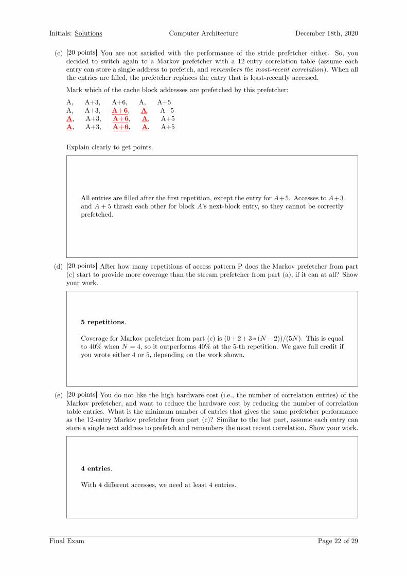
(c) [20 points] You are not satisfied with the performance of the stride prefetcher either. So, youdecided to switch again to a Markov prefetcher with a 12-entry correlation table (assume eachentry can store a single address to prefetch, and remembers the most-recent correlation). When allthe entries are filled, the prefetcher replaces the entry that is least-recently accessed.
Mark which of the cache block addresses are prefetched by this prefetcher:
A, A+3, A+6, A, A+5A, A+3, A+6, A, A+5A, A+3, A+6, A, A+5A, A+3, A+6, A, A+5
Explain clearly to get points.
All entries are filled after the first repetition, except the entry for A+5. Accesses to A+3and A+ 5 thrash each other for block A’s next-block entry, so they cannot be correctlyprefetched.
(d) [20 points] After how many repetitions of access pattern P does the Markov prefetcher from part(c) start to provide more coverage than the stream prefetcher from part (a), if it can at all? Showyour work.
5 repetitions.
Coverage for Markov prefetcher from part (c) is (0+2+3 ∗ (N − 2))/(5N). This is equalto 40% when N = 4, so it outperforms 40% at the 5-th repetition. We gave full credit ifyou wrote either 4 or 5, depending on the work shown.
(e) [20 points] You do not like the high hardware cost (i.e., the number of correlation entries) of theMarkov prefetcher, and want to reduce the hardware cost by reducing the number of correlationtable entries. What is the minimum number of entries that gives the same prefetcher performanceas the 12-entry Markov prefetcher from part (c)? Similar to the last part, assume each entry canstore a single next address to prefetch and remembers the most recent correlation. Show your work.
4 entries.
With 4 different accesses, we need at least 4 entries.
Final Exam Page 22 of 29
Initials: Solutions Computer Architecture December 18th, 2020
7 Cache Coherence [100 points]
We have a system with 4 processors {P0, P1, P2, P3} that can access memory at byte granularity. Eachprocessor has a private data cache with the following characteristics:
• Capacity of 256 bytes.
• Direct-mapped.
• Write-back.
• Block size of 64 bytes.
Each processor has also a dedicated private cache for instructions. The characteristics of the instructioncaches are not necessary to solve this question.
All data caches are connected to and actively snoop a global bus, and cache coherence is maintainedusing the MESI protocol, as we discussed in class. Note that on a write to a cache block in the S state,the block transitions directly to the M state. The range of accessible memory addresses is from 0x00000to 0xfffff.
The semantics of the instructions used in this question are as follows:
Opcode Operands Descriptionld rx,[ry] rx ← Mem[ry]st rx,[ry] rx → Mem[ry]
addi rx,#VAL rx ← rx + VALsubi rx,#VAL rx ← rx - VALj TARGET jump to TARGET
bneq rx,ry,TARGET if([rx]!=[ry]) jump to TARGET
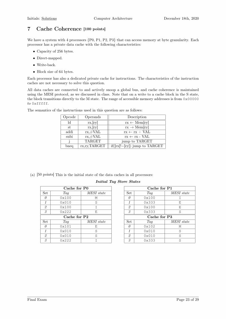
(a) [50 points] This is the initial state of the data caches in all processors:
Initial Tag Store States
Cache for P0Set Tag MESI state0 0x100 M1 0x010 S2 0x100 I3 0x222 E
Cache for P1Set Tag MESI state0 0x100 I1 0x333 E2 0x100 E3 0x333 S
Cache for P2Set Tag MESI state0 0x101 E1 0x010 S2 0x010 S3 0x222 I
Cache for P3Set Tag MESI state0 0x102 M1 0x010 S2 0x010 S3 0x333 S
Final Exam Page 23 of 29
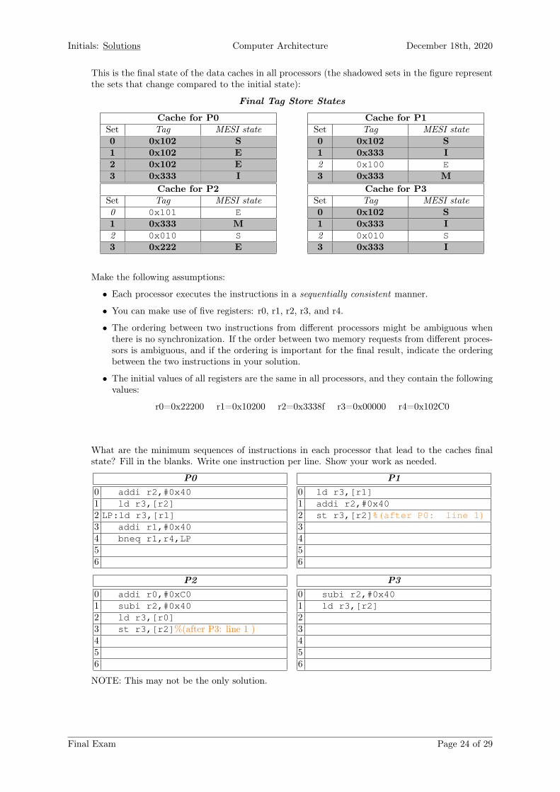
Initials: Solutions Computer Architecture December 18th, 2020
This is the final state of the data caches in all processors (the shadowed sets in the figure representthe sets that change compared to the initial state):
Final Tag Store States
Cache for P0Set Tag MESI state0 0x102 S1 0x102 E2 0x102 E3 0x333 I
Cache for P1Set Tag MESI state0 0x102 S1 0x333 I2 0x100 E3 0x333 M
Cache for P2Set Tag MESI state0 0x101 E1 0x333 M2 0x010 S3 0x222 E
Cache for P3Set Tag MESI state0 0x102 S1 0x333 I2 0x010 S3 0x333 I
Make the following assumptions:
• Each processor executes the instructions in a sequentially consistent manner.
• You can make use of five registers: r0, r1, r2, r3, and r4.
• The ordering between two instructions from different processors might be ambiguous whenthere is no synchronization. If the order between two memory requests from different proces-sors is ambiguous, and if the ordering is important for the final result, indicate the orderingbetween the two instructions in your solution.
• The initial values of all registers are the same in all processors, and they contain the followingvalues:
r0=0x22200 r1=0x10200 r2=0x3338f r3=0x00000 r4=0x102C0
What are the minimum sequences of instructions in each processor that lead to the caches finalstate? Fill in the blanks. Write one instruction per line. Show your work as needed.
P00 addi r2,#0x401 ld r3,[r2]2 LP:ld r3,[r1]3 addi r1,#0x404 bneq r1,r4,LP56
P10 ld r3,[r1]1 addi r2,#0x402 st r3,[r2]%(after P0: line 1)3456
P20 addi r0,#0xC01 subi r2,#0x402 ld r3,[r0]3 st r3,[r2]%(after P3: line 1 )456
P30 subi r2,#0x401 ld r3,[r2]23456
NOTE: This may not be the only solution.
Final Exam Page 24 of 29
Initials: Solutions Computer Architecture December 18th, 2020
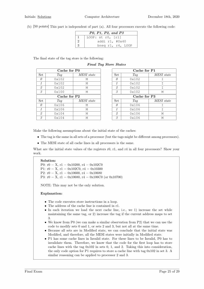
(b) [50 points] This part is independent of part (a). All four processors execute the following code:
P0, P1, P2, and P31 LOOP: st r0, [r1]2 addi r1, #0x403 bneq r1, r4, LOOP
The final state of the tag store is the following:
Final Tag Store States
Cache for P0Set Tag MESI state0 0x102 M1 0x102 M2 0x102 M3 0x100 M
Cache for P1Set Tag MESI state0 0x102 I1 0x102 I2 0x102 I3 0x102 M
Cache for P2Set Tag MESI state0 0x106 M1 0x106 M2 0x104 M3 0x104 M
Cache for P3Set Tag MESI state0 0x106 I1 0x106 I2 0x106 M3 0x106 M
Make the following assumptions about the initial state of the caches:
• The tag is the same in all sets of a processor (but the tags might be different among processors).
• The MESI state of all cache lines in all processors is the same.
What are the initial state values of the registers r0, r1, and r4 in all four processors? Show yourwork.
Solution:P0: r0 = X, r1 = 0x10200, r4 = 0x102C0P1: r0 = X, r1 = 0x102C0, r4 = 0x10300P2: r0 = X, r1 = 0x10600, r4 = 0x10680P3: r0 = X, r1 = 0x10680, r4 = 0x106C0 (or 0x10700)
NOTE: This may not be the only solution.
Explanation:
• The code executes store instructions in a loop.• The address of the cache line is contained in r1.• In each iteration we load the next cache line, i.e., we 1) increase the set whilemaintaining the same tag, or 2) increase the tag if the current address maps to set3.
• We know from P0 (we can make a similar observation from P2) that we can use thecode to modify sets 0 and 1, or sets 2 and 3, but not all at the same time.
• Because all sets are in Modified state, we can conclude that the initial state wasModified, and therefore, all the MESI states were initially in Modified state.
• P1 has some cache lines in Invalid state. For these lines to be Invalid, P0 has toinvalidate them. Therefore, we know that the code for the first loop has to storecache lines with the tag 0x102 in sets 0, 1, and 2. Taking this into consideration,the only code option for P1 requires to store a cache line with tag 0x102 in set 3. Asimilar reasoning can be applied to processor 2 and 3.
Final Exam Page 25 of 29
Initials: Solutions Computer Architecture December 18th, 2020
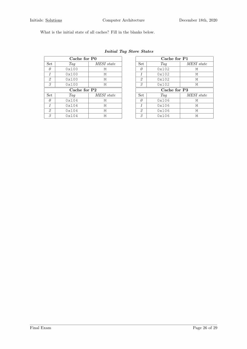
What is the initial state of all caches? Fill in the blanks below.
Initial Tag Store States
Cache for P0Set Tag MESI state0 0x100 M1 0x100 M2 0x100 M3 0x100 M
Cache for P1Set Tag MESI state0 0x102 M1 0x102 M2 0x102 M3 0x102 M
Cache for P2Set Tag MESI state0 0x104 M1 0x104 M2 0x104 M3 0x104 M
Cache for P3Set Tag MESI state0 0x106 M1 0x106 M2 0x106 M3 0x106 M
Final Exam Page 26 of 29
Initials: Solutions Computer Architecture December 18th, 2020
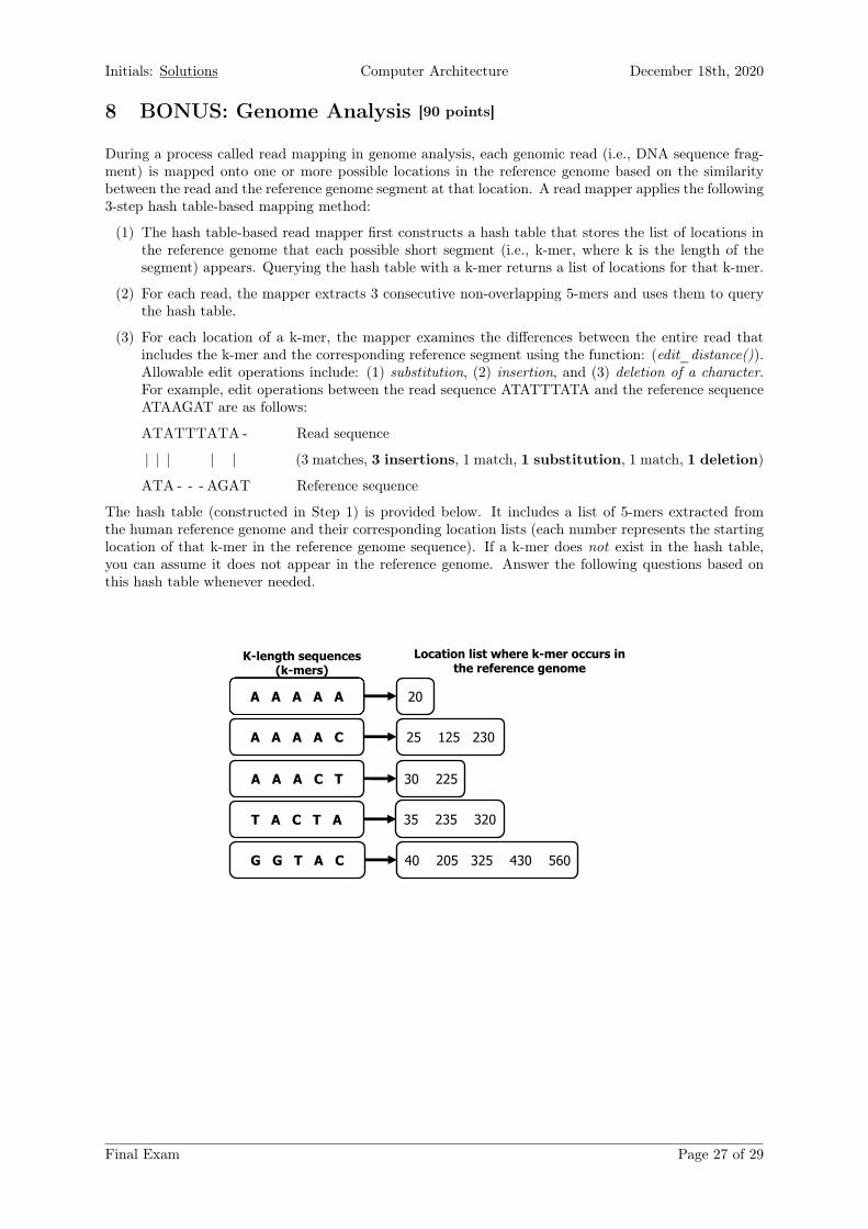
8 BONUS: Genome Analysis [90 points]
During a process called read mapping in genome analysis, each genomic read (i.e., DNA sequence frag-ment) is mapped onto one or more possible locations in the reference genome based on the similaritybetween the read and the reference genome segment at that location. A read mapper applies the following3-step hash table-based mapping method:
(1) The hash table-based read mapper first constructs a hash table that stores the list of locations inthe reference genome that each possible short segment (i.e., k-mer, where k is the length of thesegment) appears. Querying the hash table with a k-mer returns a list of locations for that k-mer.
(2) For each read, the mapper extracts 3 consecutive non-overlapping 5-mers and uses them to querythe hash table.
(3) For each location of a k-mer, the mapper examines the differences between the entire read thatincludes the k-mer and the corresponding reference segment using the function: (edit_distance()).Allowable edit operations include: (1) substitution, (2) insertion, and (3) deletion of a character.For example, edit operations between the read sequence ATATTTATA and the reference sequenceATAAGAT are as follows:
ATATTTATA - Read sequence
| | | | | (3 matches, 3 insertions, 1 match, 1 substitution, 1 match, 1 deletion)
ATA - - - AGAT Reference sequence
The hash table (constructed in Step 1) is provided below. It includes a list of 5-mers extracted fromthe human reference genome and their corresponding location lists (each number represents the startinglocation of that k-mer in the reference genome sequence). If a k-mer does not exist in the hash table,you can assume it does not appear in the reference genome. Answer the following questions based onthis hash table whenever needed.
A A A A A 20
A A A A C 25 125 230
A A A C T 30 225
T A C T A
K-length sequences (k-mers)
G G T A C 40 205 325 430 560
35 235 320
Location list where k-mer occurs in the reference genome
Final Exam Page 27 of 29
Initials: Solutions Computer Architecture December 18th, 2020
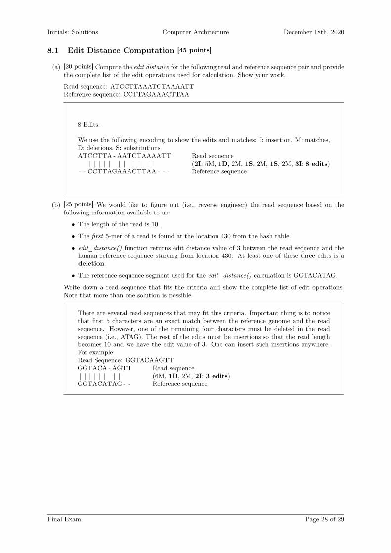
8.1 Edit Distance Computation [45 points]
(a) [20 points] Compute the edit distance for the following read and reference sequence pair and providethe complete list of the edit operations used for calculation. Show your work.
Read sequence: ATCCTTAAATCTAAAATTReference sequence: CCTTAGAAACTTAA
8 Edits.
We use the following encoding to show the edits and matches: I: insertion, M: matches,D: deletions, S: substitutionsATCCTTA - AATCTAAAATT Read sequence| | | | | | | | | | | (2I, 5M, 1D, 2M, 1S, 2M, 1S, 2M, 3I: 8 edits)
- - CCTTAGAAACTTAA - - - Reference sequence
(b) [25 points] We would like to figure out (i.e., reverse engineer) the read sequence based on thefollowing information available to us:
• The length of the read is 10.
• The first 5-mer of a read is found at the location 430 from the hash table.
• edit_distance() function returns edit distance value of 3 between the read sequence and thehuman reference sequence starting from location 430. At least one of these three edits is adeletion.
• The reference sequence segment used for the edit_distance() calculation is GGTACATAG.
Write down a read sequence that fits the criteria and show the complete list of edit operations.Note that more than one solution is possible.
There are several read sequences that may fit this criteria. Important thing is to noticethat first 5 characters are an exact match between the reference genome and the readsequence. However, one of the remaining four characters must be deleted in the readsequence (i.e., ATAG). The rest of the edits must be insertions so that the read lengthbecomes 10 and we have the edit value of 3. One can insert such insertions anywhere.For example:Read Sequence: GGTACAAGTTGGTACA - AGTT Read sequence| | | | | | | | (6M, 1D, 2M, 2I: 3 edits)GGTACATAG - - Reference sequence
Final Exam Page 28 of 29
Initials: Solutions Computer Architecture December 18th, 2020
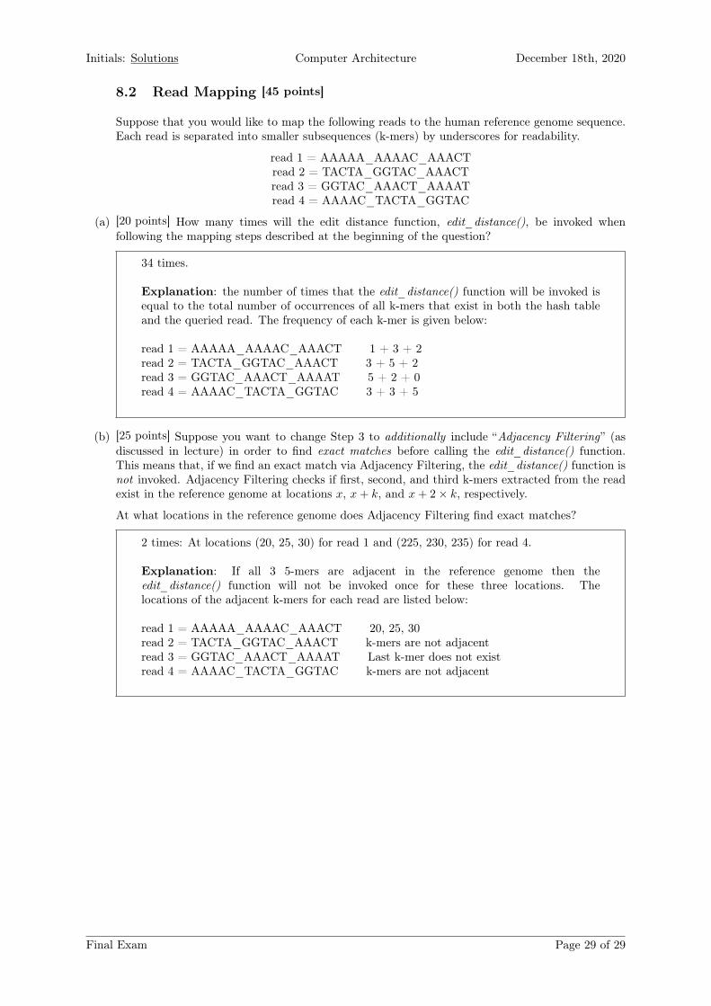
8.2 Read Mapping [45 points]
Suppose that you would like to map the following reads to the human reference genome sequence.Each read is separated into smaller subsequences (k-mers) by underscores for readability.
read 1 = AAAAA_AAAAC_AAACTread 2 = TACTA_GGTAC_AAACTread 3 = GGTAC_AAACT_AAAATread 4 = AAAAC_TACTA_GGTAC
(a) [20 points] How many times will the edit distance function, edit_distance(), be invoked whenfollowing the mapping steps described at the beginning of the question?
34 times.
Explanation: the number of times that the edit_distance() function will be invoked isequal to the total number of occurrences of all k-mers that exist in both the hash tableand the queried read. The frequency of each k-mer is given below:
read 1 = AAAAA_AAAAC_AAACT 1 + 3 + 2read 2 = TACTA_GGTAC_AAACT 3 + 5 + 2read 3 = GGTAC_AAACT_AAAAT 5 + 2 + 0read 4 = AAAAC_TACTA_GGTAC 3 + 3 + 5
(b) [25 points] Suppose you want to change Step 3 to additionally include “Adjacency Filtering” (asdiscussed in lecture) in order to find exact matches before calling the edit_distance() function.This means that, if we find an exact match via Adjacency Filtering, the edit_distance() function isnot invoked. Adjacency Filtering checks if first, second, and third k-mers extracted from the readexist in the reference genome at locations x, x+ k, and x+ 2× k, respectively.
At what locations in the reference genome does Adjacency Filtering find exact matches?
2 times: At locations (20, 25, 30) for read 1 and (225, 230, 235) for read 4.
Explanation: If all 3 5-mers are adjacent in the reference genome then theedit_distance() function will not be invoked once for these three locations. Thelocations of the adjacent k-mers for each read are listed below:
read 1 = AAAAA_AAAAC_AAACT 20, 25, 30read 2 = TACTA_GGTAC_AAACT k-mers are not adjacentread 3 = GGTAC_AAACT_AAAAT Last k-mer does not existread 4 = AAAAC_TACTA_GGTAC k-mers are not adjacent
Final Exam Page 29 of 29


