Embed Size (px)
Citation preview
15
CHAPTER THREE
System Design 3.1 System Design
Circumstances that we find ourselves in today in the field of
microcontrollers had their beginnings in the development of technology of
integrated circuits. This development has made it possible to integrate
hundreds of thousands of transistors into one chip. That was a prerequisite
for production of microprocessors, and the first computers were made by
adding external peripherals such as memory, input-output lines, timers and
other. Further increasing of the volume of the package resulted in creation of
integrated circuits. These integrated circuits contained both processor and
peripherals. That is how the first chip containing a microcomputer, or what
would later be known as a microcontroller came about. In these project we
can use various types of component.[10]
These components works to perform and satisfy the main objectives on how
to detect the location of fault ,also can be divided this components
according to design and objective in two group:
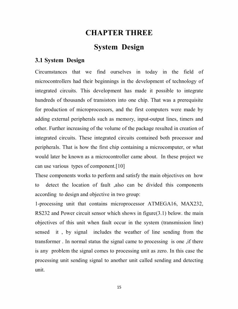
1-processing unit that contains microprocessor ATMEGA16, MAX232,
RS232 and Power circuit sensor which shows in figure(3.1) below. the main
objectives of this unit when fault occur in the system (transmission line)
sensed it , by signal includes the weather of line sending from the
transformer . In normal status the signal came to processing is one ,if there
is any problem the signal comes to processing unit as zero. In this case the
processing unit sending signal to another unit called sending and detecting
unit.
16
Figure (3.1) : contains of control unit
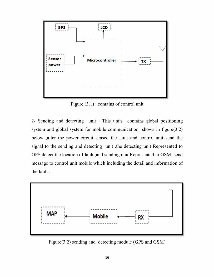
2- Sending and detecting unit : This units contains global positioning
system and global system for mobile communication shows in figure(3.2)
below ,after the power circuit sensed the fault and control unit send the
signal to the sending and detecting unit .the detecting unit Represented to
GPS detect the location of fault ,and sending unit Represented to GSM send
message to control unit mobile which including the detail and information of
the fault .
Figure(3.2) sending and detecting module (GPS and GSM)
17
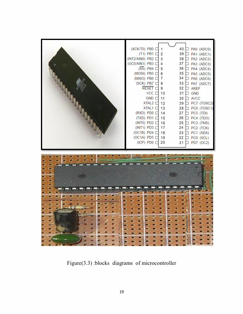
3.2 8-bit AVR Microcontroller (AT mega 16 L)
The AVR core combines a rich instruction set with 32 general purpose
working registers. All the 32 registers are directly connected to the
Arithmetic Logic Unit (ALU), allowing two independent registers to be
accessed in one single instruction executed in one clock cycle. The resulting
architecture is more code efficient while achieving throughputs up to ten
times faster than conventional CISC microcontrollers.[11]
The ATmega16 provides the following features: 16K bytes of In-System
Programmable Flash Program memory with Read-While-Write capabilities,
512 bytes EEPROM, 1K byte SRAM, 32 general purpose I/O lines, 32
general purpose working registers, a JTAG interface for Boundary-scan, On-
chip Debugging support and programming, three flexible Timer/Counters
with compare modes, Internal and External Interrupts, a serial programmable
USART, a byte oriented Two-wire Serial Interface, an 8-channel, 10-bit
ADC with optional differential input stage with programmable gain (TQFP
package only), a programmable Watchdog Timer with Internal Oscillator, an
SPI serial port, and six software selectable power saving modes. The Idle
mode stops the CPU while allowing the USART, Two-wire interface, A/D
Converter, SRAM, Timer/Counters, SPI port, and interrupt system to
continue functioning. The Power-down mode saves the register contents
but freezes the Oscillator, disabling all other chip functions until the next
External Interrupt or Hardware Reset. In Power-save mode, the
Asynchronous Timer continues to run, allowing the user to maintain a timer
base while the rest of the device is sleeping. The ADC Noise Reduction
mode stops the CPU and all I/O modules except Asynchronous Timer and
ADC, to minimize switching noise during ADC conversions. In Standby
18
mode, the crystal/resonator Oscillator is running while the rest of the device
is sleeping. This allows very fast start-up combined with low-power
consumption. In Extended Standby mode, both the main Oscillator and the
Asynchronous Timer continue to run[12]. The device is manufactured using
Atmel’s high density nonvolatile memory technology. The On-chip ISP
Flash allows the program memory to be reprogrammed in-system through an
SPI serial interface, by a conventional nonvolatile memory programmer, or
by an On-chip Boot program running on the AVR core. The boot program
can use any interface to download the application program in the
Application Flash memory. Software in the Boot Flash section will continue
to run while the Application Flash section is updated, providing true Read-
While-Write operation. By combining an 8-bit RISC CPU with In-System
Self-Programmable Flash on a monolithic chip, the Atmel ATmega16 is a
powerful microcontroller that provides a highly-flexible and cost-effective
solution to many embedded control applications. The ATmega16 AVR is
supported with a full suite of program and system development tools
including: C compilers, macro assemblers, program debugger/simulators, in-
circuit emulators, and evaluation kits.[13]
19
Figure(3.3) :blocks diagrams of microcontroller
20
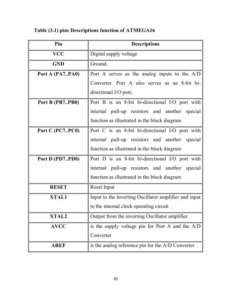
Table (3.1) pins Descriptions function of ATMEGA16
Pin Descriptions
VCC Digital supply voltage
GND Ground.
Port A (PA7..PA0) Port A serves as the analog inputs to the A/D
Converter. Port A also serves as an 8-bit bi-
directional I/O port,
Port B (PB7..PB0) Port B is an 8-bit bi-directional I/O port with
internal pull-up resistors and another special
function as illustrated in the block diagram
Port C (PC7..PC0) Port C is an 8-bit bi-directional I/O port with
internal pull-up resistors and another special
function as illustrated in the block diagram
Port D (PD7..PD0) Port D is an 8-bit bi-directional I/O port with
internal pull-up resistors and another special
function as illustrated in the block diagram
RESET Reset Input
XTAL1 Input to the inverting Oscillator amplifier and input
to the internal clock operating circuit
XTAL2 Output from the inverting Oscillator amplifier
AVCC is the supply voltage pin for Port A and the A/D
Converter
AREF is the analog reference pin for the A/D Converter
21
3.3 Global Positioning System (GPS)
It is space based satellite navigation system that provides location and time
information in all weather conditions anywhere on or near the earth where
there is unobstructed line of sight to four or more GPS Satellites. Advances
in technology and new demands on the existing system have now led to
efforts to modernize the GPS system in addition to GPS other systems are in
use or under development. The design of GPS is based partly on similar
ground based Radio Navigation systems the first Navigation satellite system
transit was used by US 1960. GPS is owned and operated by United States
as a national resource. The satellites carry very stable atomic clocks that are
synchronized to each other and to ground clocks A GPS reviver monitors
multiple satellites and solves equations to determine the exact position of the
receiver and its deviation from true time. It is sometimes above is
representative of a receiver start-up situation. Most receivers have a track
algorithm, sometimes called a tracker, that combines sets of satellite
measurements collected at different time-in effect, taking advantage of a the
fact that successive receiver positions are usually close to each other. After a
set of measurements are processed, the tracker predicts the receiver location
corresponding to the next set of satellite measurements. When the new
measurements are collected, the receiver uses a weighting scheme to
combine the new measurements with the tracker prediction. In general a
tracker can (a) improve receiver position and time accuracy, (b) reject bad
measurements, and (c) estimate receiver speed and direction.[15]
3.3.1 ACCURACY
Most receiver lose accuracy in the interpretation of the signals and are only
accurate to 100 nanoseconds.
22
GPS time is theoretically accurate to about 14 nanoseconds.
3.3.2 TIMEKEEPING
Leap seconds GPS navigation message includes the difference between
GPS time and UTS. As of July 2012, GPS time is 16 seconds ahead of UTS
because of the leap second added to UTS June. 30,2012 Receivers subtract
this offset from GPS time to calculate UTS and specific time zone values.
New GPS units may not show the correct UTS time until after receiving the
UTS offset massage. The GPS- UTS offset field can accommodate 255 leap
second (eight bits)
3.3.3 ERROR SOURCES AND ANALYSIS
Magnitude of residual errors from these sources depends on geometric
dilution of precision. Artificial errors may result from jamming devices and
threaten ships and aircraft or from intentional signed degradation through
selective availability, which limited accuracy to- 6-12 m, but has now been
switched off
3.3.4 STRUCTURE
The space segment is composed of 24 to 32 satellites in medium earth orbit
and also includes the payload adapters to the boosters required to launch
them into orbit. The control segment is composed of a master control station
(MCS), an alternate master control station, and a host of dedicated and
shared ground antennas and monitor stations. The user segment is composed
of hundreds of thousands of U.S. and allied military users of the secure GPS
Precise Positioning Service and tens of millions of civil, commercial, and
scientific user of the Standard Positioning Service The period of the carrier
frequency multiplied by the speed of light gives the wavelength, which is
about 0.19 meters. Accuracy within 1% of wavelength in detecting the
23
leading edge reduces this component of pseudo range error to as little as 2
millimeters. [15]
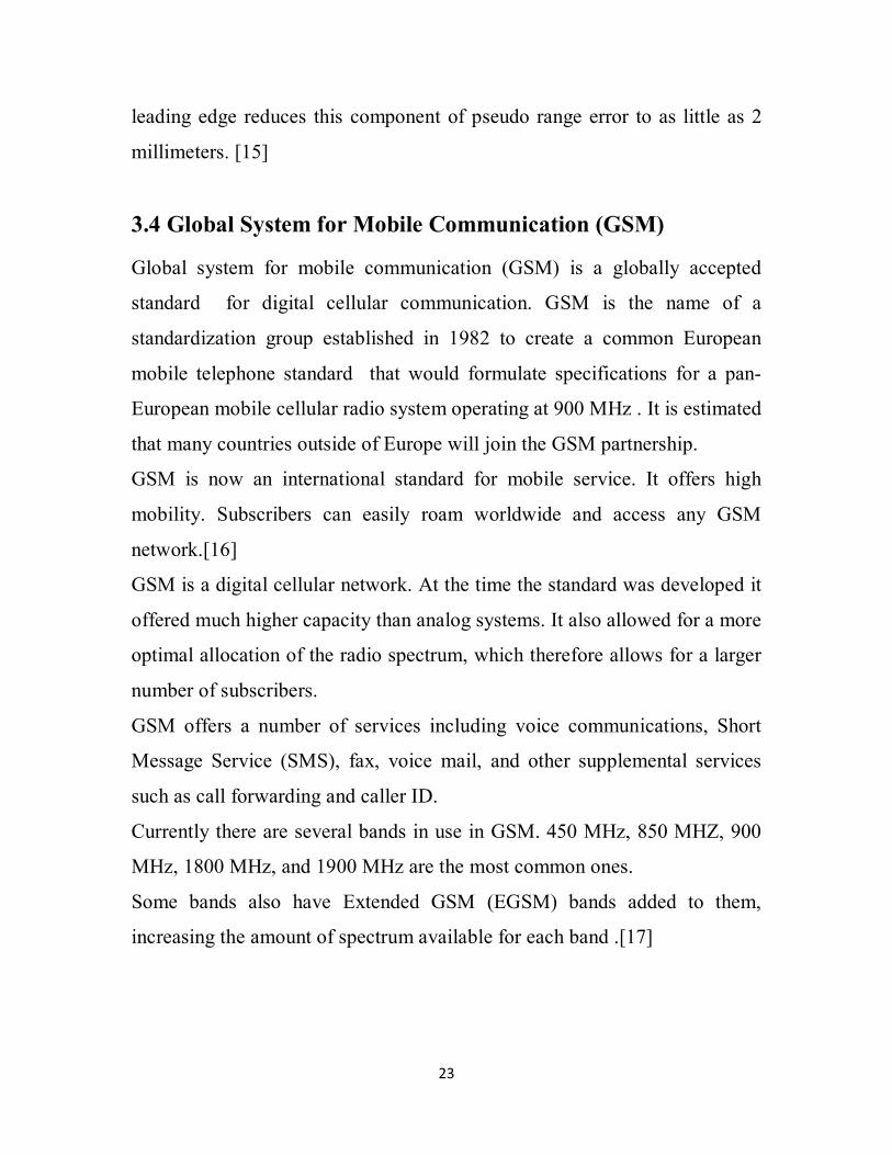
3.4 Global System for Mobile Communication (GSM)
Global system for mobile communication (GSM) is a globally accepted
standard for digital cellular communication. GSM is the name of a
standardization group established in 1982 to create a common European
mobile telephone standard that would formulate specifications for a pan-
European mobile cellular radio system operating at 900 MHz . It is estimated
that many countries outside of Europe will join the GSM partnership.
GSM is now an international standard for mobile service. It offers high
mobility. Subscribers can easily roam worldwide and access any GSM
network.[16]
GSM is a digital cellular network. At the time the standard was developed it
offered much higher capacity than analog systems. It also allowed for a more
optimal allocation of the radio spectrum, which therefore allows for a larger
number of subscribers.
GSM offers a number of services including voice communications, Short
Message Service (SMS), fax, voice mail, and other supplemental services
such as call forwarding and caller ID.
Currently there are several bands in use in GSM. 450 MHz, 850 MHZ, 900
MHz, 1800 MHz, and 1900 MHz are the most common ones.
Some bands also have Extended GSM (EGSM) bands added to them,
increasing the amount of spectrum available for each band .[17]
24
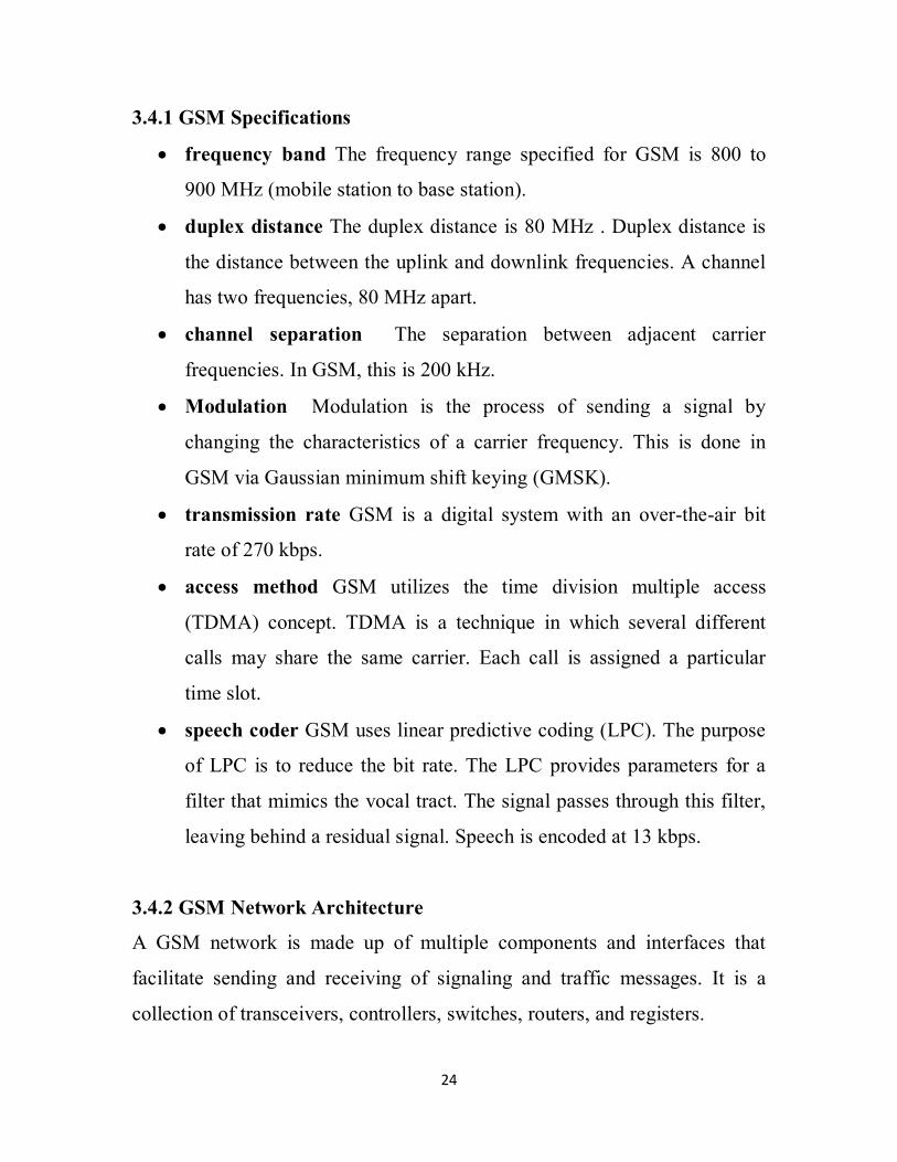
3.4.1 GSM Specifications
frequency band The frequency range specified for GSM is 800 to
900 MHz (mobile station to base station).
duplex distance The duplex distance is 80 MHz . Duplex distance is
the distance between the uplink and downlink frequencies. A channel
has two frequencies, 80 MHz apart.
channel separation The separation between adjacent carrier
frequencies. In GSM, this is 200 kHz.
Modulation Modulation is the process of sending a signal by
changing the characteristics of a carrier frequency. This is done in
GSM via Gaussian minimum shift keying (GMSK).
transmission rate GSM is a digital system with an over-the-air bit
rate of 270 kbps.
access method GSM utilizes the time division multiple access
(TDMA) concept. TDMA is a technique in which several different
calls may share the same carrier. Each call is assigned a particular
time slot.
speech coder GSM uses linear predictive coding (LPC). The purpose
of LPC is to reduce the bit rate. The LPC provides parameters for a
filter that mimics the vocal tract. The signal passes through this filter,
leaving behind a residual signal. Speech is encoded at 13 kbps.
3.4.2 GSM Network Architecture
A GSM network is made up of multiple components and interfaces that
facilitate sending and receiving of signaling and traffic messages. It is a
collection of transceivers, controllers, switches, routers, and registers.
25
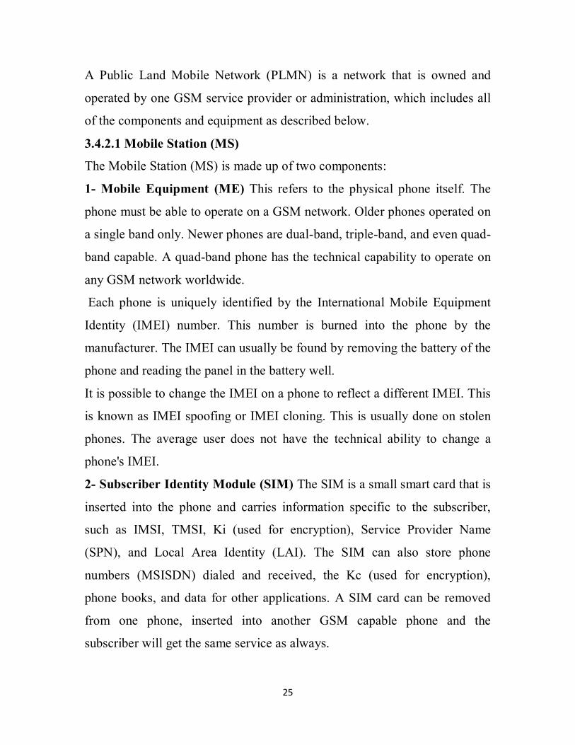
A Public Land Mobile Network (PLMN) is a network that is owned and
operated by one GSM service provider or administration, which includes all
of the components and equipment as described below.
3.4.2.1 Mobile Station (MS)
The Mobile Station (MS) is made up of two components:
1- Mobile Equipment (ME) This refers to the physical phone itself. The
phone must be able to operate on a GSM network. Older phones operated on
a single band only. Newer phones are dual-band, triple-band, and even quad-
band capable. A quad-band phone has the technical capability to operate on
any GSM network worldwide.
Each phone is uniquely identified by the International Mobile Equipment
Identity (IMEI) number. This number is burned into the phone by the
manufacturer. The IMEI can usually be found by removing the battery of the
phone and reading the panel in the battery well.
It is possible to change the IMEI on a phone to reflect a different IMEI. This
is known as IMEI spoofing or IMEI cloning. This is usually done on stolen
phones. The average user does not have the technical ability to change a
phone's IMEI.
2- Subscriber Identity Module (SIM) The SIM is a small smart card that is
inserted into the phone and carries information specific to the subscriber,
such as IMSI, TMSI, Ki (used for encryption), Service Provider Name
(SPN), and Local Area Identity (LAI). The SIM can also store phone
numbers (MSISDN) dialed and received, the Kc (used for encryption),
phone books, and data for other applications. A SIM card can be removed
from one phone, inserted into another GSM capable phone and the
subscriber will get the same service as always.
26
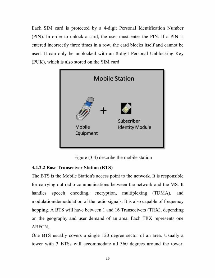
Each SIM card is protected by a 4-digit Personal Identification Number
(PIN). In order to unlock a card, the user must enter the PIN. If a PIN is
entered incorrectly three times in a row, the card blocks itself and cannot be
used. It can only be unblocked with an 8-digit Personal Unblocking Key
(PUK), which is also stored on the SIM card
Figure (3.4) describe the mobile station
3.4.2.2 Base Transceiver Station (BTS)
The BTS is the Mobile Station's access point to the network. It is responsible
for carrying out radio communications between the network and the MS. It
handles speech encoding, encryption, multiplexing (TDMA), and
modulation/demodulation of the radio signals. It is also capable of frequency
hopping. A BTS will have between 1 and 16 Transceivers (TRX), depending
on the geography and user demand of an area. Each TRX represents one
ARFCN.
One BTS usually covers a single 120 degree sector of an area. Usually a
tower with 3 BTSs will accommodate all 360 degrees around the tower.
27
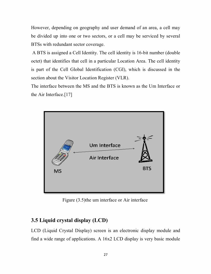
However, depending on geography and user demand of an area, a cell may
be divided up into one or two sectors, or a cell may be serviced by several
BTSs with redundant sector coverage.
A BTS is assigned a Cell Identity. The cell identity is 16-bit number (double
octet) that identifies that cell in a particular Location Area. The cell identity
is part of the Cell Global Identification (CGI), which is discussed in the
section about the Visitor Location Register (VLR).
The interface between the MS and the BTS is known as the Um Interface or
the Air Interface.[17]
Figure (3.5)the um interface or Air interface
3.5 Liquid crystal display (LCD)
LCD (Liquid Crystal Display) screen is an electronic display module and
find a wide range of applications. A 16x2 LCD display is very basic module
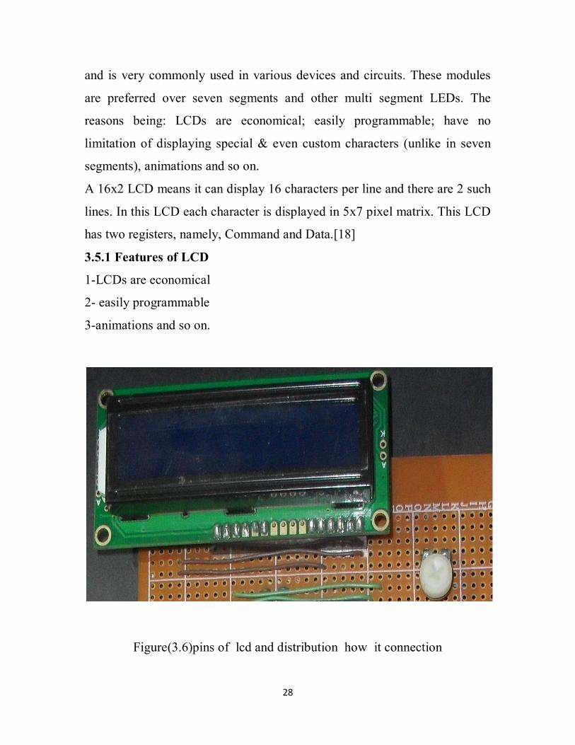
28
and is very commonly used in various devices and circuits. These modules
are preferred over seven segments and other multi segment LEDs. The
reasons being: LCDs are economical; easily programmable; have no
limitation of displaying special & even custom characters (unlike in seven
segments), animations and so on.
A 16x2 LCD means it can display 16 characters per line and there are 2 such
lines. In this LCD each character is displayed in 5x7 pixel matrix. This LCD
has two registers, namely, Command and Data.[18]
3.5.1 Features of LCD
1-LCDs are economical
2- easily programmable
3-animations and so on.
Figure(3.6)pins of lcd and distribution how it connection
29
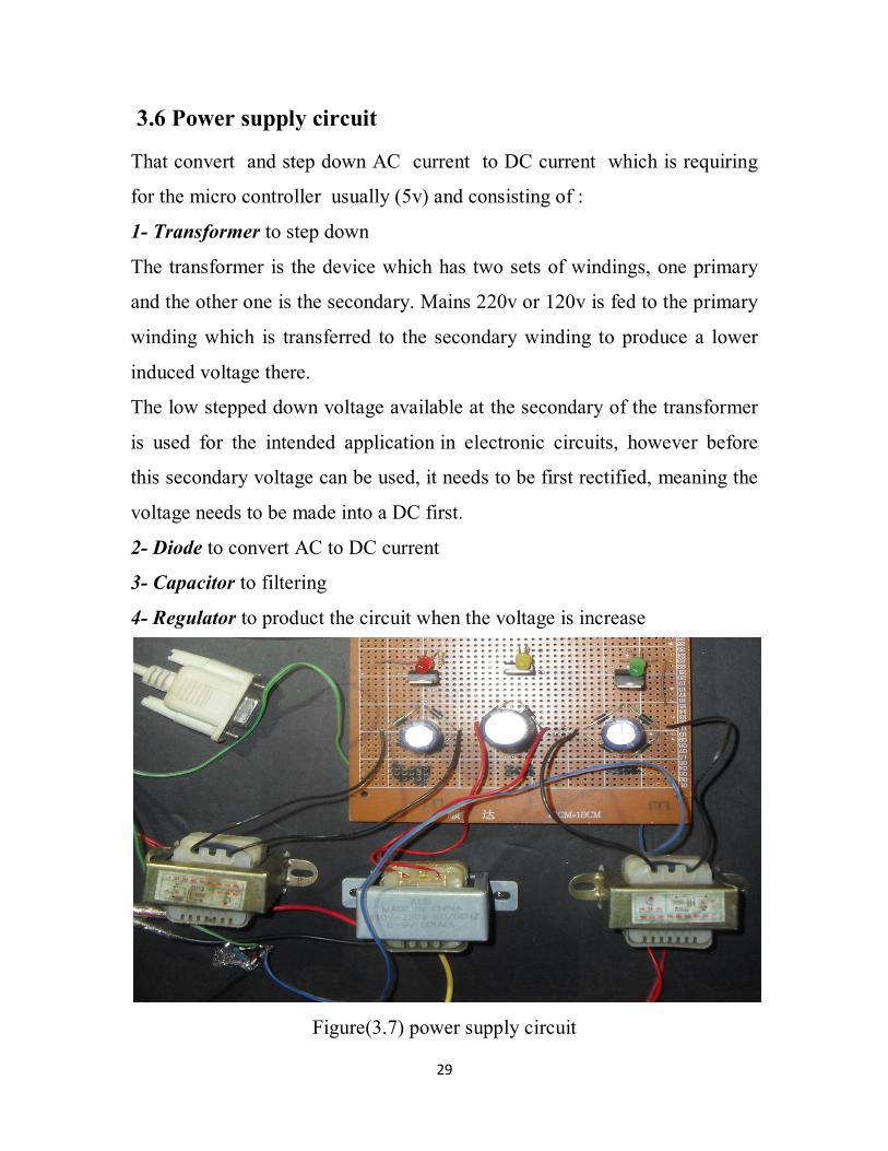
3.6 Power supply circuit
That convert and step down AC current to DC current which is requiring
for the micro controller usually (5v) and consisting of :
1- Transformer to step down
The transformer is the device which has two sets of windings, one primary
and the other one is the secondary. Mains 220v or 120v is fed to the primary
winding which is transferred to the secondary winding to produce a lower
induced voltage there.
The low stepped down voltage available at the secondary of the transformer
is used for the intended application in electronic circuits, however before
this secondary voltage can be used, it needs to be first rectified, meaning the
voltage needs to be made into a DC first.
2- Diode to convert AC to DC current
3- Capacitor to filtering
4- Regulator to product the circuit when the voltage is increase
Figure(3.7) power supply circuit
30
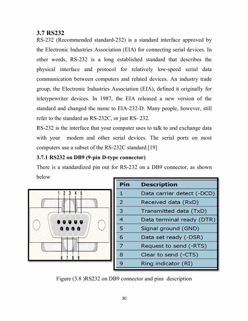
3.7 RS232 RS-232 (Recommended standard-232) is a standard interface approved by
the Electronic Industries Association (EIA) for connecting serial devices. In
other words, RS-232 is a long established standard that describes the
physical interface and protocol for relatively low-speed serial data
communication between computers and related devices. An industry trade
group, the Electronic Industries Association (EIA), defined it originally for
teletypewriter devices. In 1987, the EIA released a new version of the
standard and changed the name to EIA-232-D. Many people, however, still
refer to the standard as RS-232C, or just RS- 232.
RS-232 is the interface that your computer uses to talk to and exchange data
with your modem and other serial devices. The serial ports on most
computers use a subset of the RS-232C standard.[19]
3.7.1 RS232 on DB9 (9-pin D-type connector)
There is a standardized pin out for RS-232 on a DB9 connector, as shown
below
Figure (3.8 )RS232 on DB9 connector and pins description
31
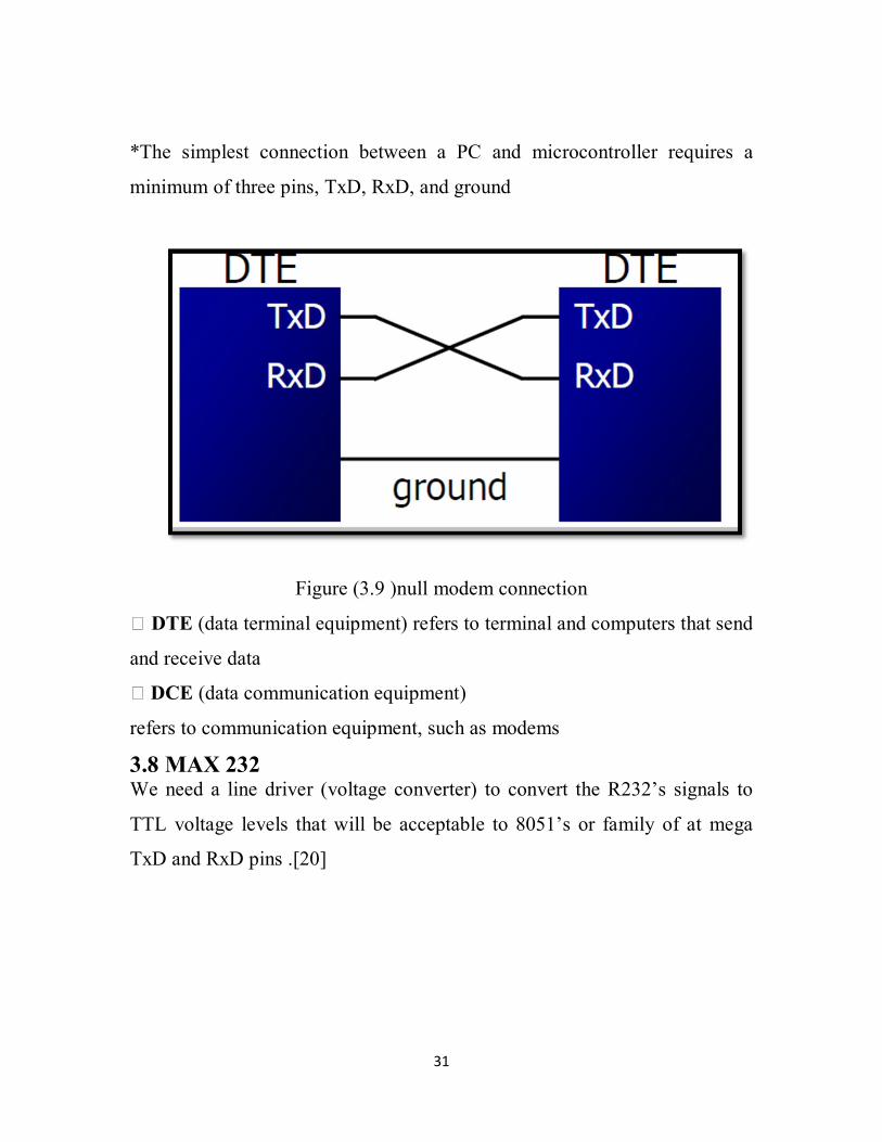
*The simplest connection between a PC and microcontroller requires a
minimum of three pins, TxD, RxD, and ground
Figure (3.9 )null modem connection
DTE (data terminal equipment) refers to terminal and computers that send
and receive data
DCE (data communication equipment)
refers to communication equipment, such as modems
3.8 MAX 232 We need a line driver (voltage converter) to convert the R232’s signals to
TTL voltage levels that will be acceptable to 8051’s or family of at mega
TxD and RxD pins .[20]
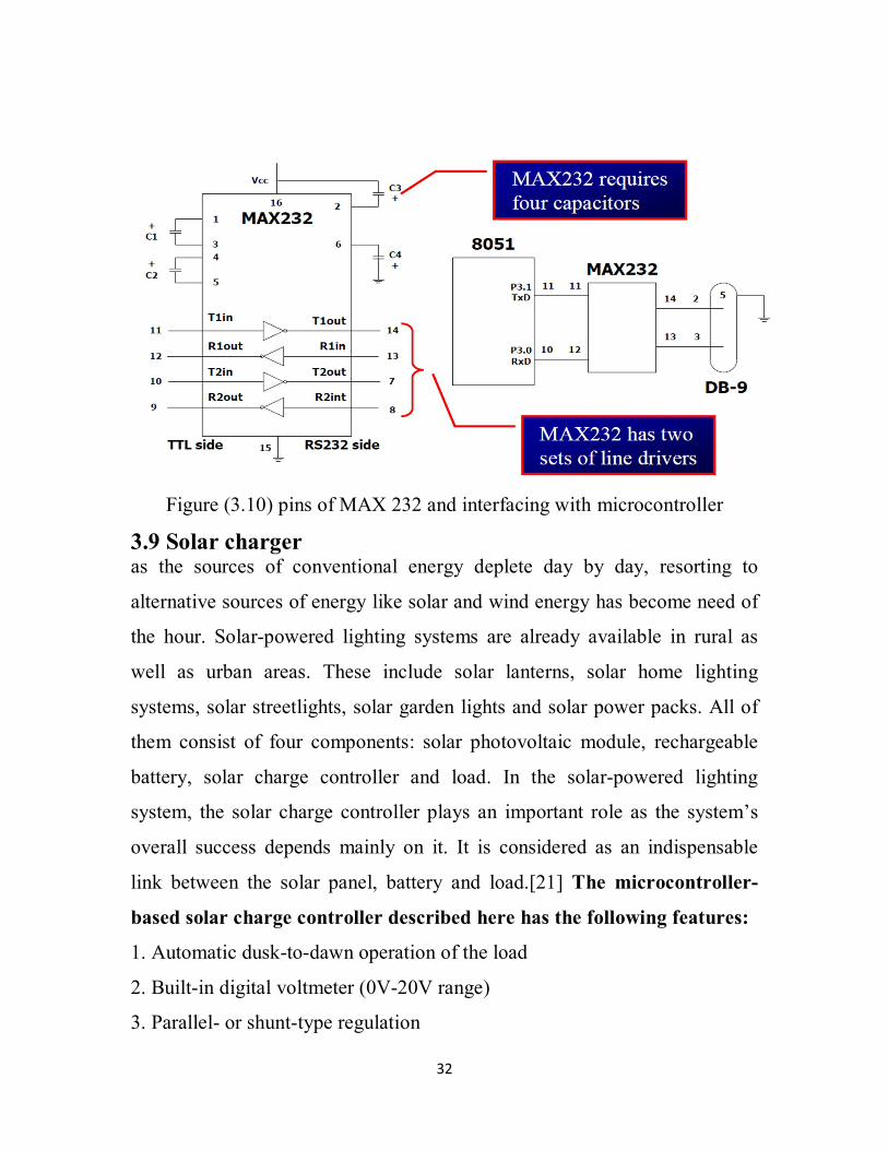
32
Figure (3.10) pins of MAX 232 and interfacing with microcontroller
3.9 Solar charger as the sources of conventional energy deplete day by day, resorting to
alternative sources of energy like solar and wind energy has become need of
the hour. Solar-powered lighting systems are already available in rural as
well as urban areas. These include solar lanterns, solar home lighting
systems, solar streetlights, solar garden lights and solar power packs. All of
them consist of four components: solar photovoltaic module, rechargeable
battery, solar charge controller and load. In the solar-powered lighting
system, the solar charge controller plays an important role as the system’s
overall success depends mainly on it. It is considered as an indispensable
link between the solar panel, battery and load.[21] The microcontroller-
based solar charge controller described here has the following features:
1. Automatic dusk-to-dawn operation of the load
2. Built-in digital voltmeter (0V-20V range)
3. Parallel- or shunt-type regulation
33
4. Charging current changes to ‘pulsed’ at full charge
5. Low current consumption
6. Highly efficient design based on microcontroller
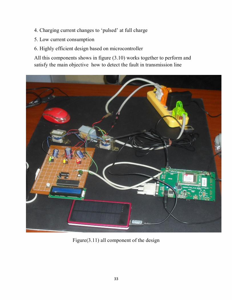
All this components shows in figure (3.10) works together to perform and satisfy the main objective how to detect the fault in transmission line
Figure(3.11) all component of the design


