Embed Size (px)
Citation preview
Characteristics of ultra-compact polymer modulators based on silicon photonic crystal ring resonators
Zexuan Qiang,a Weidong Zhou,a Richard A. Soref,b and Zhenqiang Mac aDepartment of Electrical Engineering, NanoFAB Center
University of Texas at Arlington, TX 76019, USA [email protected]
b Sensors Directorate, Air Force Research Laboratory, AFRL/RYHC Hanscom Air Force Base, MA 01731, USA
cDepartment of Electrical and Computer Engineering University of Wisconsin-Madison, WI 53706, USA
Abstract. Ultra-compact polymer modulators were proposed and simulated, based on the hybrid integration of functional polymer materials with Si based photonic-crystal ring resonators (PCRRs). The simulations were carried out on device characteristics with an effective ring radius of 2.3 µm and tunable polymer index from 1.785 to 1.805. Investigating the loss, the cavity quality factor Q, and the free spectral range of such PCRRs, we found a 0.02 dB intrinsic loss that is independent of diameter, unlike the loss that varies inversely with diameter in microstrip resonators. Close to 100% drop efficiency at the drop channel of 1557.5 nm was obtained by design with a high spectral selectivity of Q greater than 1319 in the single-ring PCRR-based add-drop filters with ring radius of 1.2 µm.
Keywords: Photonic crystals, ring resonators, silicon modulators, polymer photonics, RF photonics.
1 INTRODUCTION There is an increasing and largely unfulfilled need for nanometer-scale photonic components, both passive and active, in intra-chip optical communications and other high-speed, ultra-low-power photonic applications. Some of the most compact microphotonic components developed for 1550 nm use, such as microring-resonator modulators [1-6], have a minimum useable diameter (D) of about 25 λ/n, where λ is the free-space wavelength and n is the refractive index of the silicon-on-insulator strip (or rib) waveguide from which the ring is made. In the field of nanophotonics, it is desirable to scale D downwards in future versions of the device. However, the 1/D dependence of propagation loss in the microstrip [5, 7] presents an obstacle to scaling [7].
On the other hand, photonic crystals offer great promise in ultra-compact photonic components. Photonic crystal add-drop filters (ADFs) have been reported with various defect and cavity configurations, with a single-defect cavity as the smallest resonators [8-13]. Recently we proposed and reported photonic-crystal ring resonators (PCRRs), with scalable ring sizes and flexible mode coupling configurations [14]. Potentially, PCRRs can have a minimum D of around 5 λ/n. This may present a solution to the 1/D dependent loss problem-- if it can be shown that the PCRR insertion loss will be significantly lower than that of a micro- ring which has same diameter. Additionally, the issue of whether the PCRR also satisfies the well-known relationship between free spectral range (FSR) and ring radius R of traditional micro-strip ring resonators hasn’t been addressed yet.
Polymer-based electro-optical modulators have attracted great attention due to their intrinsic high performance like low loss, low birefringence, high thermo-optic coefficient,
Journal of Nanophotonics, Vol. 2, 023507 (22 May 2008)
© 2008 Society of Photo-Optical Instrumentation Engineers [DOI: 10.1117/1.2943640]Received 12 Apr 2008; accepted 21 May 2008; published 22 May 2008 [CCC: 19342608/2008/$25.00]Journal of Nanophotonics, Vol. 2, 023507 (2008) Page 1
environmental stability, and high yields with easy processibility [15, 16]. There are two general structures to implement ultrafast polymer modulators: the Mach-Zehnder Interferometer (MZI) [17, 18] and the microring-resonator [19-21] based structure. Traveling wave MZI polymer modulators require several millimeters of optical path (or even ~ 1 cm) to achieve the desired phase shift, which brings phase matching problems to the RF design because the electrode length is comparable to RF wavelength. However in micro-ring modulators, the electrode loss is not an issue and the bandwidth is set by the electrode capacitance. The device is small enough to allow the electrode size to be much smaller than the modulation wavelength, even up to 100 GHz [22], and the device’s high-speed behavior is mainly capacitive. Here we propose a new hybrid integration of functional polymer materials with Si rods-based PCRRs, which can lead to ultra-compact, high-speed modulators suitable for photonic integration and RF photonics.
In what follows, we first present a detailed analysis of the feasibility of ultra-compact low-propagation-loss PCRRs as compared to the traditional micro-strip rings with effective radius from 1 to 15 µm at λ ~ 1550 nm by using the two-dimensional finite-difference time-domain (FDTD) technique with perfectly matched layers (PML) as absorbing boundaries. We then investigate the performance of the hybrid polymer/silicon PCRR modulator including its tuning ability and the effect of surrounding PC periods on resonator’s quality factor. The results are favorable.
2 ANALYSIS OF LOW-LOSS ULTRA-COMPACT SILICON-ROD-BASED PCRRS
For traditional micro-strip ring resonators the relationship between FSR and R is [19]:
RnR
nn
FSRgeff
effπ
λ
πλ
λ
λλ2
2)()(
22
⋅=
⋅∂
∂−
=∆ , (1)
where λ is the resonant wavelength, while neff and ng are the effective index and the group index of the ring, respectively. The group velocity can be further derived from
dkdc
vcng
g /ϖ== , (2)
where c is the speed of light in vacuum, vg is the group velocity, equal to dω/dk. We here attempted to use the same equation (1) to analyze the spectral characteristics of PCRR structures. The group velocity vg can be obtained from the dispersion curve for the confined defect mode in the single-line-defect bus waveguide [23] after which the group index ng is found. We first introduce an effective radius concept for the PCRR structure based upon the equivalent area concept, as shown in Fig. 1(a) (right), with
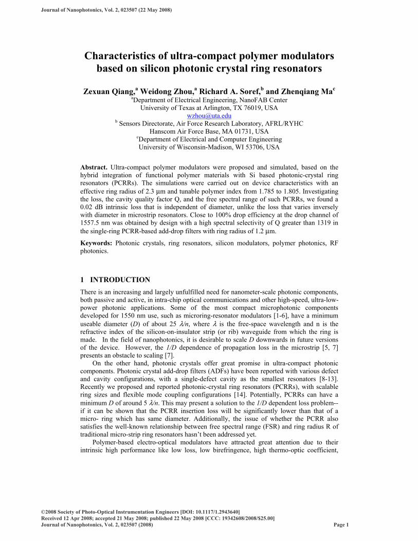
π/)1( amReff += , (3) where m is the number of dielectric rods or air holes enclosed in the PCRR resonator (m = 3 for the structure shown). By changing the m values, the effective radius changes accordingly. Finally, we can get the free spectral relationship of PCRRs by using the defined effective radius and the derived group index in equation (1).
For comparison, a two-dimensional single-ring optical ADF fashioned from silicon micro-strip (“nano wires”) is schematically shown in Fig. 1(b), where the incident port and the exit ports are labeled as A, B, C, D, respectively. The structure in Fig. 1(a) is based on a square lattice of high-index dielectric rods (nh, 3.48) surrounded by the background of low index (nl) materials. The low index materials can be silica or polymer with index of 1.48-1.78, or simply air (nl = 1). Comparable ADF performances can be obtained for both cases. Note that in Fig. 1(a) four additional dielectric-rod scatterers (blue color) with the same parameters
Journal of Nanophotonics, Vol. 2, 023507 (2008) Page 2
(size and index) as all other dielectric rods were introduced to improve the spectral selectivity and drop efficiency [14]. In this section, we only report the results for the air background case since the Si micro-strip-ring-based ADFs are surrounded by air as well. In Fig. 1(a), the ratio of the rod radius r to the lattice constant a, is 0.185. Based on the simulated photonic dispersion curves (see the inset of Fig. 3 (b)), the photonic bandgap is present from 1270 to 1740 nm for the lattice constant a of 540nm.
(a) Photonic crystal ring resonators
A B
CD
A B
CD
A
D
B
C
R
(b) Micro-strip ring resonators
Width W
Gap t
Reff
a
Reff
a
(a) Photonic crystal ring resonators
A B
CD
A B
CD
A
D
B
C
R
(b) Micro-strip ring resonators
Width W
Gap t
Width W
Gap t
Reff
a
Reff
a
Reff
a
Reff
a
Fig. 1. (a) Schematic of photonic crystal ring resonators with effective radius Reff defined as shown in the right plot; (b) Micro-strip ring resonators and the associated radius R.
In the present comparison, ADFs based on micro-strip ring resonators having similar configuration parameters are used to simulate the transmission and loss properties, as shown in Fig. 1 (b), where the effective index and group index are both equal to 2.44, while the strip width and gap size are W = 500 nm and t = 100 nm, respectively. The lengths of the waveguide buses are kept the same for all cases in these two structures, which is L = 33.5 µm (or 62a for PCRR-based ADFs). A sequence of decreasing ring radii R is investigated in our size dependent loss analysis. Generally, there is a trade-off between an increase of the cavity Q and the associated decrease of the coupling/dropping efficiency [14]. The coupling strength, i.e., the number of coupling periods between the line defect waveguide bus and the PCRRs, was adjusted for high drop efficiency. The bus-ring coupling distance changed from two periods for small ring sizes (e.g., the one shown in Fig. 1(a)), to three periods when the Reff of PCRR increased to 2.44 µm and greater (m > 7).
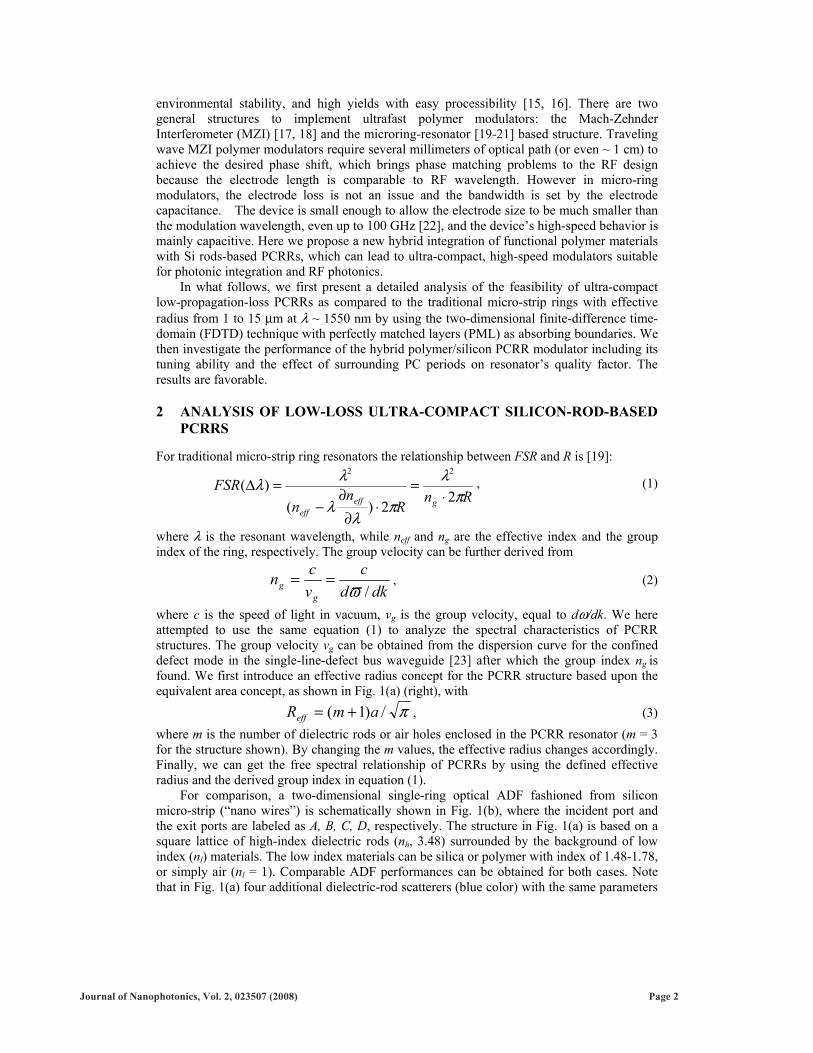
The transmission characteristics were then simulated with 2D FDTD using perfectly matched layers (PML) as absorbing boundaries [14]. A Gaussian optical pulse, covering the whole frequency-range-of-interest is launched at the input port A. Power monitors were placed at each of the other three ports (B, C, D) to collect the transmitted spectral power density after Fourier transformation. All of the transmitted spectral power densities were normalized to the incident light spectral power density at Port A. Simulations were carried out for Silicon PCRR and micro-strip-ring-resonator-based ADFs. Shown in Fig. 2(a) are the normalized transmission spectra for three output ports (B, C, D) in the single-ring ADFs. Close to 100% drop efficiency at the drop channel of 1557.5 nm was obtained with a high spectral selectivity of Q greater than 1319 in the single-ring PCRR-based ADFs with 1.2 µm effective radius. We determined that the spectral performance reported here is comparable to or better than that of the micro-strip ring resonators aswith even large ring radius (R = 3 µm) as shown in Fig. 2(b). The field patterns for the drop channels with different ring sizes for
Journal of Nanophotonics, Vol. 2, 023507 (2008) Page 3
PCRRs and for the micro-strip ring resonators are shown in Fig. 2(c). The total normalized power at three output ports (B+C+D)/A is used to derive the total loss in the ADF devices, in units of dBs. It is worth mentioning that the total loss in the ADF devices derived here includes both the bending loss associated with small ring-radius PCRRs as well as the coupling loss between the waveguide buses and the PCRRs.
1552 1556 15600204060
80100
Wavelength (nm)T
(%)
B
C
D
1400 1440 1480 1520 1560 16000
20
40
60
80
100
Wavelength (nm)
Nor
mal
ized
tran
smis
sion
(%) m=3
Reff = 1.218 µm
R=3µmB
DC
1480 1500 1520 1540 1560 15800
20
40
60
80
100
Wavelength (nm)
Nor
mal
ized
tran
smis
sion
(%)
(a)
(b) (c)
PCRR: m = 3
PCRR: m = 15
Micro-strip RR
1552 1556 15600204060
80100
Wavelength (nm)T
(%)
B
C
D
1400 1440 1480 1520 1560 16000
20
40
60
80
100
Wavelength (nm)
Nor
mal
ized
tran
smis
sion
(%) m=3
Reff = 1.218 µm
1552 1556 15600204060
80100
Wavelength (nm)T
(%)
1552 1556 15600204060
80100
Wavelength (nm)T
(%)
B
C
D
1400 1440 1480 1520 1560 16000
20
40
60
80
100
Wavelength (nm)
Nor
mal
ized
tran
smis
sion
(%)
B
C
D
1400 1440 1480 1520 1560 16000
20
40
60
80
100
Wavelength (nm)
Nor
mal
ized
tran
smis
sion
(%)
1400 1440 1480 1520 1560 16000
20
40
60
80
100
Wavelength (nm)
Nor
mal
ized
tran
smis
sion
(%) m=3
Reff = 1.218 µm
R=3µmB
DC
1480 1500 1520 1540 1560 15800
20
40
60
80
100
Wavelength (nm)
Nor
mal
ized
tran
smis
sion
(%)
R=3µmB
DC
1480 1500 1520 1540 1560 15800
20
40
60
80
100
Wavelength (nm)
Nor
mal
ized
tran
smis
sion
(%)
(a)
(b) (c)
PCRR: m = 3
PCRR: m = 15
Micro-strip RR
Fig. 2. Spectral response of single ring add-drop filters based on (a) PCRRs; (b) Micro-strip ring resonators. Shown in (c) are the field patterns for the corresponding drop channels with different ring sizes for PCRRs and micro-strip ring resonators.
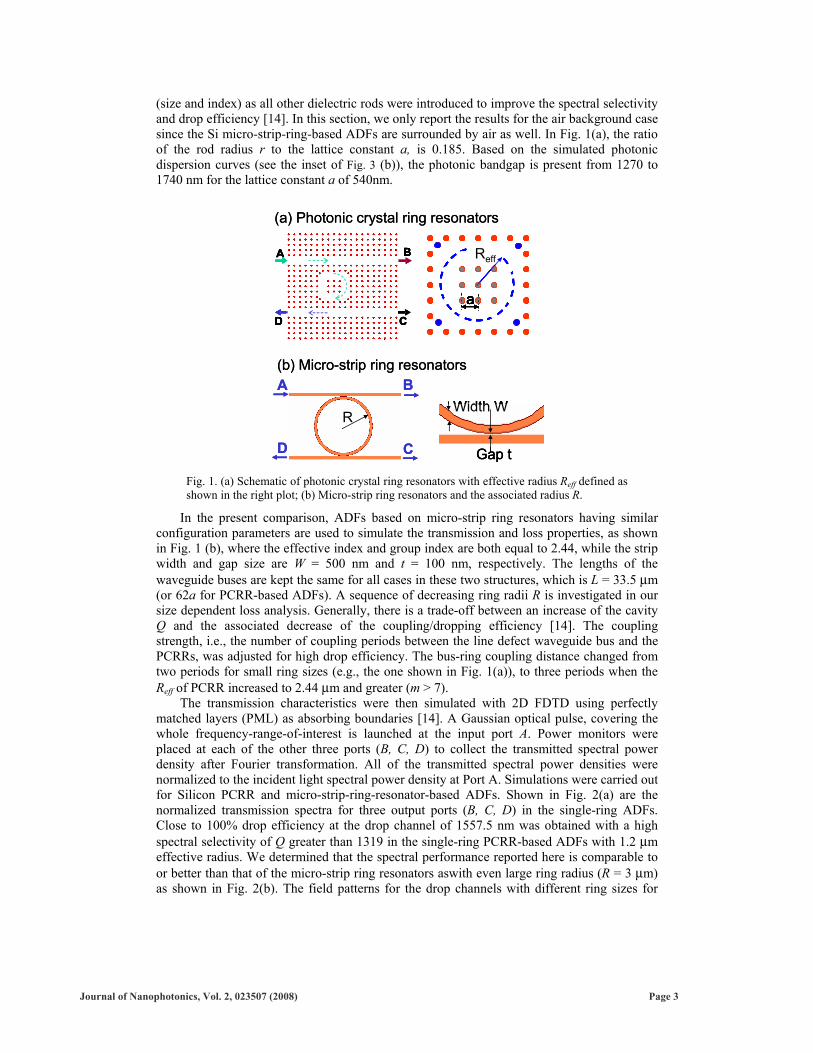
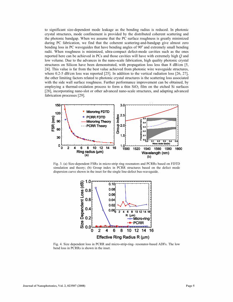
The size-dependent free-spectral range (FSR) values were investigated and compared for both PCRRs and micro-strip ring resonators. One set of the data is plotted in Fig. 3 (a) which is derived from the simulated spectral response curves, as shown in Fig. 2, for different radii. It is interesting to note that the change in FSR associated with effective radius in PCRRs follows closely the FSR change for micro-strip-based ring resonators. We tried to fit the FDTD data with the theoretical equation (1). The ng result is shown in Fig. 3 (b) for different Reff. The dispersion plot for a single line-defect bus-waveguide is shown in the inset of Fig. 3 (b) which was simulated with the plane-wave expansion technique. Theoretical FSR values were calculated for each radius with different resonator wavelength and the corresponding group index based on Fig. 3 (b). As shown in Fig. 3 (a), very good agreement was obtained between theory and FDTD simulation for both structures.
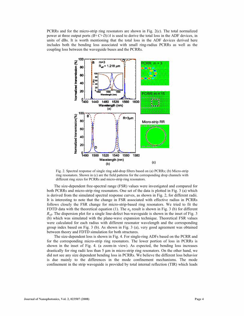
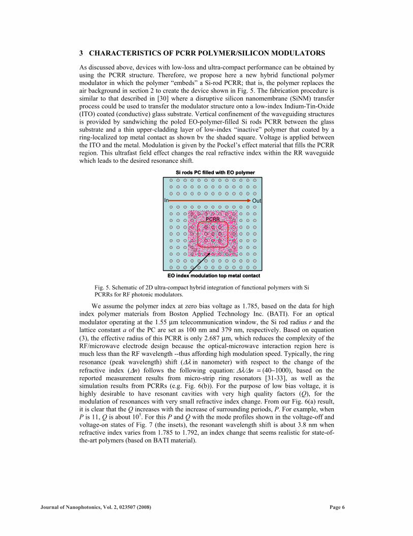
The size-dependent loss is shown in Fig. 4. For single-ring ADFs based on the PCRR and for the corresponding micro-strip ring resonators. The lower portion of loss in PCRRs is shown in the inset of Fig. 4. (a zoom-in view). As expected, the bending loss increases drastically for ring radii less than 5 µm in micro-strip ring resonators. On the other hand, we did not see any size dependent bending loss in PCRRs. We believe the different loss behavior is due mainly to the differences in the mode confinement mechanisms. The mode confinement in the strip waveguide is provided by total internal reflection (TIR) which leads
Journal of Nanophotonics, Vol. 2, 023507 (2008) Page 4
to significant size-dependent mode leakage as the bending radius is reduced. In photonic crystal structures, mode confinement is provided by the distributed coherent scattering and the photonic bandgap. When we assume that the PC surface roughness is greatly minimized during PC fabrication, we find that the coherent scattering-and-bandgap give almost zero bending loss in PC waveguides that have bending angles of 90o and extremely small bending radii. When roughness is minimized, ultra-compact defect-mode cavities such as the ones reported here can be achieved in PCs and those cavities will have with extremely high Q and low volume. Due to the advances in the nano-scale fabrication, high quality photonic crystal structures on Silicon have been demonstrated, with propagation loss less than 8 dB/cm [5, 24]. This value is far from the best value achieved from photonic wire waveguide structures, where 0.2-5 dB/cm loss was reported [25]. In addition to the vertical radiation loss [26, 27], the other limiting factors related to photonic crystal structures is the scattering loss associated with the side wall surface roughness. Further performance improvement can be obtained, by employing a thermal-oxidation process to form a thin SiO2 film on the etched Si surfaces [28], incorporating nano-slot or other advanced nano-scale structures, and adapting advanced fabrication processes [29].
0 2 4 6 8 10 12 14 160
30
60
90
120
150
Ring radius (µm)
FSR
(nm
)
Microring FDTD
PCRR FDTDMicroring TheoryPCRR Theory
(a)
0 2 4 6 8 10 12 14 160
30
60
90
120
150
Ring radius (µm)
FSR
(nm
)
Microring FDTD
PCRR FDTDMicroring TheoryPCRR Theory
0 2 4 6 8 10 12 14 160
30
60
90
120
150
Ring radius (µm)
FSR
(nm
)
0 2 4 6 8 10 12 14 160
30
60
90
120
150
Ring radius (µm)
FSR
(nm
)
Microring FDTD
PCRR FDTDMicroring TheoryPCRR Theory
Microring FDTD
PCRR FDTDMicroring TheoryPCRR Theory
(a)
Wave vector (ka/2π)Fr
eque
ncy
(ωa/
2πc=
a/λ)
0.5
0.4
0.3
0.2
0.1
0.00.0 0.1 0.2 0.3 0.4 0.5
Wave vector (ka/2π)Fr
eque
ncy
(ωa/
2πc=
a/λ)
0.5
0.4
0.3
0.2
0.1
0.00.0 0.1 0.2 0.3 0.4 0.5
( )
(b)
1500 1520 1540 1560 1580 16001.0
1.5
2.0
2.5
3.0
Wavelength (nm)
Gro
up in
dex
Wave vector (ka/2π)Fr
eque
ncy
(ωa/
2πc=
a/λ)
0.5
0.4
0.3
0.2
0.1
0.00.0 0.1 0.2 0.3 0.4 0.5
Wave vector (ka/2π)Fr
eque
ncy
(ωa/
2πc=
a/λ)
0.5
0.4
0.3
0.2
0.1
0.00.0 0.1 0.2 0.3 0.4 0.5
( )
(b)
1500 1520 1540 1560 1580 16001.0
1.5
2.0
2.5
3.0
Wavelength (nm)
Gro
up in
dex
1500 1520 1540 1560 1580 16001.0
1.5
2.0
2.5
3.0
Wavelength (nm)
Gro
up in
dex
Fig. 3. (a) Size-dependent FSRs in micro-strip ring resonators and PCRRs based on FDTD simulation and theory; (b) Group index in PCRR structures based on the defect mode dispersion curve shown in the inset for the single line-defect bus-waveguide.
0 2 4 6 8 10 12 14 160.0
0.2
0.4
0.6
0.8
1.0
Effective Ring Radius R (µm)
Siz
e D
epen
dent
Los
s (d
B)
Micro-ringPCRR
0 2 4 6 8 10 12 14 160.000.020.040.060.080.10
R (µm)0 2 4 6 8 10 12 14 160.00
0.020.040.060.080.10
R (µm)
0 2 4 6 8 10 12 14 160.0
0.2
0.4
0.6
0.8
1.0
Effective Ring Radius R (µm)
Siz
e D
epen
dent
Los
s (d
B)
Micro-ringPCRR
0 2 4 6 8 10 12 14 160.0
0.2
0.4
0.6
0.8
1.0
Effective Ring Radius R (µm)
Siz
e D
epen
dent
Los
s (d
B)
Micro-ringPCRRMicro-ringPCRR
0 2 4 6 8 10 12 14 160.000.020.040.060.080.10
R (µm)0 2 4 6 8 10 12 14 160.00
0.020.040.060.080.10
R (µm)
Fig. 4. Size dependent loss in PCRR and micro-strip-ring- resonator-based ADFs. The low bend loss in PCRRs is shown in the inset.
Journal of Nanophotonics, Vol. 2, 023507 (2008) Page 5
3 CHARACTERISTICS OF PCRR POLYMER/SILICON MODULATORS
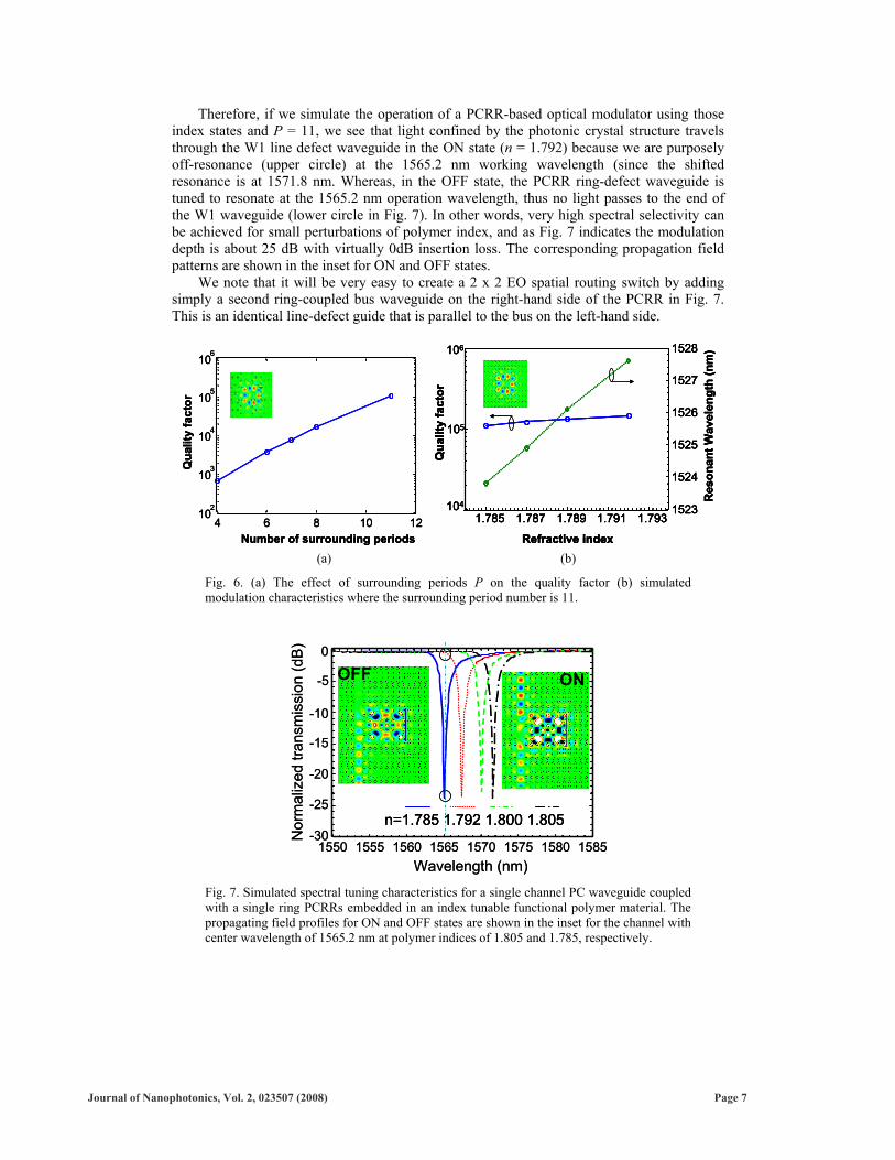
As discussed above, devices with low-loss and ultra-compact performance can be obtained by using the PCRR structure. Therefore, we propose here a new hybrid functional polymer modulator in which the polymer “embeds” a Si-rod PCRR; that is, the polymer replaces the air background in section 2 to create the device shown in Fig. 5. The fabrication procedure is similar to that described in [30] where a disruptive silicon nanomembrane (SiNM) transfer process could be used to transfer the modulator structure onto a low-index Indium-Tin-Oxide (ITO) coated (conductive) glass substrate. Vertical confinement of the waveguiding structures is provided by sandwiching the poled EO-polymer-filled Si rods PCRR between the glass substrate and a thin upper-cladding layer of low-index “inactive” polymer that coated by a ring-localized top metal contact as shown bv the shaded square. Voltage is applied between the ITO and the metal. Modulation is given by the Pockel’s effect material that fills the PCRR region. This ultrafast field effect changes the real refractive index within the RR waveguide which leads to the desired resonance shift.
In Out
PCRR
EO index modulation top metal contact
Si rods PC filled with EO polymer
In Out
PCRR
EO index modulation top metal contact
Si rods PC filled with EO polymer
Fig. 5. Schematic of 2D ultra-compact hybrid integration of functional polymers with Si PCRRs for RF photonic modulators.
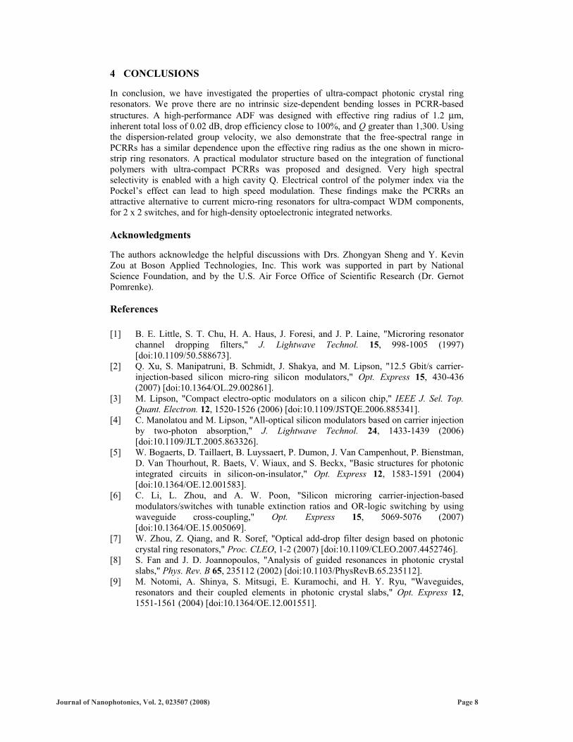
We assume the polymer index at zero bias voltage as 1.785, based on the data for high index polymer materials from Boston Applied Technology Inc. (BATI). For an optical modulator operating at the 1.55 µm telecommunication window, the Si rod radius r and the lattice constant a of the PC are set as 100 nm and 379 nm, respectively. Based on equation (3), the effective radius of this PCRR is only 2.687 µm, which reduces the complexity of the RF/microwave electrode design because the optical-microwave interaction region here is much less than the RF wavelength --thus affording high modulation speed. Typically, the ring resonance (peak wavelength) shift (∆λ in nanometer) with respect to the change of the refractive index (∆n) follows the following equation: ∆λ/∆n = (40−1000), based on the reported measurement results from micro-strip ring resonators [31-33], as well as the simulation results from PCRRs (e.g. Fig. 6(b)). For the purpose of low bias voltage, it is highly desirable to have resonant cavities with very high quality factors (Q), for the modulation of resonances with very small refractive index change. From our Fig. 6(a) result, it is clear that the Q increases with the increase of surrounding periods, P. For example, when P is 11, Q is about 105. For this P and Q with the mode profiles shown in the voltage-off and voltage-on states of Fig. 7 (the insets), the resonant wavelength shift is about 3.8 nm when refractive index varies from 1.785 to 1.792, an index change that seems realistic for state-of-the-art polymers (based on BATI material).
Journal of Nanophotonics, Vol. 2, 023507 (2008) Page 6
Therefore, if we simulate the operation of a PCRR-based optical modulator using those index states and P = 11, we see that light confined by the photonic crystal structure travels through the W1 line defect waveguide in the ON state (n = 1.792) because we are purposely off-resonance (upper circle) at the 1565.2 nm working wavelength (since the shifted resonance is at 1571.8 nm. Whereas, in the OFF state, the PCRR ring-defect waveguide is tuned to resonate at the 1565.2 nm operation wavelength, thus no light passes to the end of the W1 waveguide (lower circle in Fig. 7). In other words, very high spectral selectivity can be achieved for small perturbations of polymer index, and as Fig. 7 indicates the modulation depth is about 25 dB with virtually 0dB insertion loss. The corresponding propagation field patterns are shown in the inset for ON and OFF states.
We note that it will be very easy to create a 2 x 2 EO spatial routing switch by adding simply a second ring-coupled bus waveguide on the right-hand side of the PCRR in Fig. 7. This is an identical line-defect guide that is parallel to the bus on the left-hand side.
4 6 8 10 1210
2
103
104
105
106
Number of surrounding periods
Qua
lity
fact
or
4 6 8 10 1210
2
103
104
105
106
Number of surrounding periods
Qua
lity
fact
or
4 6 8 10 1210
2
103
104
105
106
Number of surrounding periods
Qua
lity
fact
or
106
Qua
lity
fact
or105
104
1.785 1.787 1.789 1.791 1.793
Refractive index
1523
1524
1525
1526
1527
1528
Res
onan
t Wav
elen
gth
(nm
)106
Qua
lity
fact
or105
104
1.785 1.787 1.789 1.791 1.793
Refractive index
1523
1524
1525
1526
1527
1528
Res
onan
t Wav
elen
gth
(nm
)106
Qua
lity
fact
or105
104
1.785 1.787 1.789 1.791 1.793
Refractive index
1523
1524
1525
1526
1527
1528
Res
onan
t Wav
elen
gth
(nm
)106
Qua
lity
fact
or105
104
1.785 1.787 1.789 1.791 1.793
Refractive index
1523
1524
1525
1526
1527
1528
Res
onan
t Wav
elen
gth
(nm
)
(a) (b)
Fig. 6. (a) The effect of surrounding periods P on the quality factor (b) simulated modulation characteristics where the surrounding period number is 11.
1550 1555 1560 1565 1570 1575 1580 1585-30
-25
-20
-15
-10
-5
0
Wavelength (nm)
Nor
mal
ized
tran
smis
sion
(dB
)
OFF
n=1.785 1.792 1.800 1.805
ON
1550 1555 1560 1565 1570 1575 1580 1585-30
-25
-20
-15
-10
-5
0
Wavelength (nm)
Nor
mal
ized
tran
smis
sion
(dB
)
OFF
n=1.785 1.792 1.800 1.805n=1.785 1.792 1.800 1.805
ON
Fig. 7. Simulated spectral tuning characteristics for a single channel PC waveguide coupled with a single ring PCRRs embedded in an index tunable functional polymer material. The propagating field profiles for ON and OFF states are shown in the inset for the channel with center wavelength of 1565.2 nm at polymer indices of 1.805 and 1.785, respectively.
Journal of Nanophotonics, Vol. 2, 023507 (2008) Page 7
4 CONCLUSIONS
In conclusion, we have investigated the properties of ultra-compact photonic crystal ring resonators. We prove there are no intrinsic size-dependent bending losses in PCRR-based structures. A high-performance ADF was designed with effective ring radius of 1.2 µm, inherent total loss of 0.02 dB, drop efficiency close to 100%, and Q greater than 1,300. Using the dispersion-related group velocity, we also demonstrate that the free-spectral range in PCRRs has a similar dependence upon the effective ring radius as the one shown in micro-strip ring resonators. A practical modulator structure based on the integration of functional polymers with ultra-compact PCRRs was proposed and designed. Very high spectral selectivity is enabled with a high cavity Q. Electrical control of the polymer index via the Pockel’s effect can lead to high speed modulation. These findings make the PCRRs an attractive alternative to current micro-ring resonators for ultra-compact WDM components, for 2 x 2 switches, and for high-density optoelectronic integrated networks.
Acknowledgments
The authors acknowledge the helpful discussions with Drs. Zhongyan Sheng and Y. Kevin Zou at Boson Applied Technologies, Inc. This work was supported in part by National Science Foundation, and by the U.S. Air Force Office of Scientific Research (Dr. Gernot Pomrenke). References [1] B. E. Little, S. T. Chu, H. A. Haus, J. Foresi, and J. P. Laine, "Microring resonator
channel dropping filters," J. Lightwave Technol. 15, 998-1005 (1997) [doi:10.1109/50.588673].
[2] Q. Xu, S. Manipatruni, B. Schmidt, J. Shakya, and M. Lipson, "12.5 Gbit/s carrier-injection-based silicon micro-ring silicon modulators," Opt. Express 15, 430-436 (2007) [doi:10.1364/OL.29.002861].
[3] M. Lipson, "Compact electro-optic modulators on a silicon chip," IEEE J. Sel. Top. Quant. Electron. 12, 1520-1526 (2006) [doi:10.1109/JSTQE.2006.885341].
[4] C. Manolatou and M. Lipson, "All-optical silicon modulators based on carrier injection by two-photon absorption," J. Lightwave Technol. 24, 1433-1439 (2006) [doi:10.1109/JLT.2005.863326].
[5] W. Bogaerts, D. Taillaert, B. Luyssaert, P. Dumon, J. Van Campenhout, P. Bienstman, D. Van Thourhout, R. Baets, V. Wiaux, and S. Beckx, "Basic structures for photonic integrated circuits in silicon-on-insulator," Opt. Express 12, 1583-1591 (2004) [doi:10.1364/OE.12.001583].
[6] C. Li, L. Zhou, and A. W. Poon, "Silicon microring carrier-injection-based modulators/switches with tunable extinction ratios and OR-logic switching by using waveguide cross-coupling," Opt. Express 15, 5069-5076 (2007) [doi:10.1364/OE.15.005069].
[7] W. Zhou, Z. Qiang, and R. Soref, "Optical add-drop filter design based on photonic crystal ring resonators," Proc. CLEO, 1-2 (2007) [doi:10.1109/CLEO.2007.4452746].
[8] S. Fan and J. D. Joannopoulos, "Analysis of guided resonances in photonic crystal slabs," Phys. Rev. B 65, 235112 (2002) [doi:10.1103/PhysRevB.65.235112].
[9] M. Notomi, A. Shinya, S. Mitsugi, E. Kuramochi, and H. Y. Ryu, "Waveguides, resonators and their coupled elements in photonic crystal slabs," Opt. Express 12, 1551-1561 (2004) [doi:10.1364/OE.12.001551].
Journal of Nanophotonics, Vol. 2, 023507 (2008) Page 8
[10] J. Romero-Vivas, D. Chigrin, A. Lavrinenko, and C. Sotomayor Torres, "Resonant add-drop filter based on a photonic quasicrystal," Opt. Express 13, 826-835 (2005) [doi:10.1364/OPEX.13.000826].
[11] Z. Zhang and M. Qiu, "Compact in-plane channel drop filter design using a single cavity with two degenerate modes in 2D photonic crystal slabs," Opt. Express 13, 2596-2604 (2005) [doi:10.1364/OE.13.002596].
[12] H. Takano, B. S. Song, T. Asano, and S. Noda, "Highly efficient in-plane channel drop filter in a two-dimensional heterophotonic crystal," Appl. Phys. Lett. 86, 241101 (2005) [doi:10.1063/1.1941458].
[13] H. Takano, Y. Akahane, T. Asano, and S. Noda, "In-plane-type channel drop filter in a two-dimensional photonic crystal slab," Appl. Phys. Lett. 84, 2226 (2004) [doi:10.1063/1.1689742].
[14] Z. Qiang, W. D. Zhou, and R. A. Soref, "Optical add-drop filters based on photonic crystal ring resonators," Opt. Express 15, 1823-1831 (2007) [doi:10.1364/OE.15.001823].
[15] J. H. Burroughes and C. Jones, "New semiconductor device physics in polymer diodes and transistors," Nature 335, 137-141 (1988) [doi:10.1038/335137a0].
[16] L. Eldada, "Polymer integrated optics: Promise vs. practicality," Proc. SPIE 4642, 11-22 (2002) [doi:10.1117/12.470454].
[17] W. H. Steier, A. Chen, S. S. Lee, S. Garner, H. Zhang, V. Chuyanov, L. R. Dalton, F. Wang, A. S. Ren, and C. Zhang, "Polymer electro-optic devices for integrated optics," Chem. Phys. 245, 487-506 (1999) [doi:10.1016/S0301-0104(99)00042-7].
[18] R. M. de Ridder, A. Driessen, E. Rikkers, P. V. Lambeck, and M. B. J. Diemeer, "Design and fabrication of electro-optic polymer modulators and switches," Opt. Mater. 12, 205-214 (1999) [doi:10.1016/S0925-3467(99)00048-8].
[19] P. Rabiei, W. H. Steier, C. Zhang, and L. R. Dalton, "Polymer micro-ring filters and modulators," J. Lightwave Tech. 20, 1968-1975 (2002) [doi:10.1109/JLT.2002.803058].
[20] A. Leinse, M. B. J. Diemeer, A. Rousseau, and A. Driessen, "A novel high-speed polymeric EO modulator based on a combination of a microring resonator and an MZI," IEEE Photon. Technol. Lett. 17, 2074-2076 (2005) [doi:10.1109/LPT.2005.854354].
[21] H. Tazawa, Y. H. Kuo, I. Dunayevskiy, J. Luo, A. K. Y. Jen, H. R. Fetterman, and W. H. Steier, "Ring resonator-based electrooptic polymer traveling-wave modulator," J. Lightwave Technol. 24, 3514–3519 (2006) [doi:10.1109/JLT.2006.878514].
[22] R. T. Chen, "Polymer-based photonic integrated circuits," Optic. Laser Technol. 25, 347–365 (1993) [doi:10.1016/0030-3992(93)90001-V].
[23] S.-H. Jeong, N. Yamamoto, J. Sugisaka, M. Okano, and K. Komori, "GaAs-based two-dimensional photonic crystal slab ring resonator consisting of a directional coupler and bent waveguides," J. Opt. Soc. Am. B 24, 1951-1959 (2007) [doi:10.1364/JOSAB.24.001951].
[24] Y. A. Vlasov, M. O'Boyle, H. F. Hamann, and S. J. McNab, "Active control of slow light on a chip with photonic crystal waveguides," Nature 438, 65-69 (2005) [doi:10.1038/nature04210].
[25] Y. Vlasov and S. McNab, "Losses in single-mode silicon-on-insulator strip waveguides and bends," Opt. Express 12, 1622-1631 (2004) [doi:10.1364/OPEX.12.001622].
[26] T. Baba, A. Motegi, T. Iwai, N. Fukaya, Y. Watanabe, and A. Sakai, "Light propagation characteristics of straight single-line-defectwaveguides in photonic crystal slabs fabricated into asilicon-on-insulator substrate," IEEE J. Quant. Electron. 38, 743-752 (2002) [doi:10.1109/JQE.2002.1017584].
Journal of Nanophotonics, Vol. 2, 023507 (2008) Page 9
[27] W. Kuang and J. D. O'Brien, "Reducing the out-of-plane radiation loss of photonic crystal waveguides on high-index substrates," Opt. Lett. 29, 860-862 (2004) [doi:10.1364/OL.29.000860].
[28] Y. Jiang, W. Jiang, L. Gu, X. Chen, and R. T. Chen, "80-micron interaction length silicon photonic crystal waveguide modulator," Appl. Phys. Lett. 87, 221105 (2005) [doi:10.1063/1.2138367].
[29] M. Lipson, "Guiding, modulating and emitting light on silicon - challenges and opportunities," J. Lightwave Technol. 23, 4222-4238 (2005) [doi:10.1109/JLT.2005.858225].
[30] H. C. Yuan, Z. Ma, M. M. Roberts, D. E. Savage, and M. G. Lagally, "High-speed strained-single-crystal-silicon thin-film transistors on flexible polymers," J. Appl. Phys. 100, 13708-13708 (2006) [doi:10.1063/1.2214301].
[31] V. R. Almeida, C. A. Barrios, R. R. Panepucci, and M. Lipson, "All-optical control of light on a silicon chip," Nature 431, 1081-1084 (2004) [doi:10.1038/nature02921].
[32] M. Lipson, "Overcoming the limitations of microelectronics using Si nanophotonics: solving the coupling, modulation and switching challenges," Nanotechnol. 15, S622-S627 (2004) [doi:10.1088/0957-4484/15/10/020].
[33] E. Chow, A. Grot, L. W. Mirkarimi, M. Sigalas, and G. Girolami, "Ultracompact biochemical sensor built with two-dimensional photonic crystal microcavity," Opt. Lett. 29, 1093-1095 (2004) [doi:10.1364/OL.29.001093].
Journal of Nanophotonics, Vol. 2, 023507 (2008) Page 10


