Embed Size (px)
Citation preview

Surface and Coatings Technology 151–152(2002) 194–203
0257-8972/02/$ - see front matter� 2002 Elsevier Science B.V. All rights reserved.PII: S0257-8972Ž01.01619-X
Characterization of nitride coatings by XPS
I. Bertoti*´
Chemical Research Center , Hungarian Academy of Sciences, Research Laboratory of Materials and Environmental Chemistry, P.O. Box 17,,1
H-1525 Budapest, Hungary
Abstract
Nitride coatings have been used in numerous applications to increase the hardness and improve the wear and corrosionresistance of structural materials, as well as in various high-tech areas, where their functional rather than mechanical propertiesare of prime importance. Performance of these coatings is equally dependent on their chemical composition and long-rangecrystalline structure, as well as on the nature and amount of impurities and intergranular interactions. Significant improvement inthe mechanical properties has recently been achieved with multi-component superlattice and nanocomposite nitride coatings. Inthe case of such multi-component systems, not only is close control of the elemental composition(stoichiometry) necessary tooptimize the properties of the coatings, but the influence of chemical bond formation between the components is also of primeimportance. Special care needs to be taken when non-equilibrium preparation conditions, activation of CVD and PVD by plasmasor energetic particle beams are applied, occasionally leading to unpredicted deviations, both in composition and structure. As ishighlighted in this paper, nitride coatings or nitrided surfaces can be analyzed in detail by X-ray photoelectron spectroscopy(XPS) due to its excellent element selectivity, quantitative character and high surface sensitivity. More importantly, XPS reflectsthe atomic scale chemical interactions, i.e. the bonds between neighboring atoms, and thus it also provides reliable structuralcharacteristics for amorphous or nano-crystalline coatings of complex composition, for which application of diffraction techniquesis not straightforward. A number of examples of the application of XPS are given for various types of nitride coatings, includinginterstitial compounds, such as TiN, CrN , etc., as well as compounds with predominantly covalent bonding, such as AlN, GaN,x
Si N and CN . Special emphasis is placed on ion beam-induced compositional and structural changes and to the formation of3 4 x
‘superstoichiometric’ TiN , ZrN compounds.� 2002 Elsevier Science B.V. All rights reserved.1qx 1qx
Keywords: Nitrides; Nitride coatings; X-Ray photoelectron spectroscopy(XPS); X-Ray-induced Auger electron spectroscopy(XAES)
1. Introduction
Nitride coatings deposited by physical(PVD) andchemical vapor deposition(CVD) and layers created onthe surface of a workpiece by plasma treatment or ionimplantation have gained wide structural application inimproving the wear resistance, oxidation and corrosionprotection of machining tools and engineering compo-nents. In addition, they are broadly used as functionaland as decorative coatings. Among the functional appli-cations, microelectronics and optics should be mentionedfirst. Due to the biocompatibility of TiN, it can beapplied in orthopedic and dental implants. Atomicallysmooth surfaces of CN coatings make them applicablex
* Tel.: q36-1-325-8147; fax:q36-1-325-7892.E-mail address: [email protected](I. Bertoti).´http:y ywww.chemres.huyAKKL1
as protective layers for high-density magnetic storagemedia. In other high-tech fields, new multi-component,nano-structured or multi-layered superlattice coatingswith new combinations of beneficial structural andfunctional properties are attracting much interest andutilization w1–4x.The determination of the crystallographic phases pres-
ent in these films is usually carried out by X-raydiffraction (XRD), which allows overall identificationof the crystalline phases. However, in the case of dual-or multiple-phase coatings with very low grain size,exact determination of the individual phases by XRDcan be ambiguous due to overlapping peaks or peakbroadening. In addition to these ambiguities, minorphases of atomic–molecular dimensions constituting theinterface between the crystalline grains may be over-looked in XRD. Consequently, this technique cannotgive a complete characterization of a nitride coating ora thin nitrided surface layer.

195I. Bertoti / Surface and Coatings Technology 151 –152 (2002) 194–203´
Fig. 1. The N 1s lineshape recorded for various nitride coatings(top) and the result of peak generation for the N 1s peak envelope of a CNx
sample(bottom).
As far as the chemical composition is concerned,exact determination of the nitrogen content in thinsurface films(similar to carbon in carbide coatings) hasremained problematic. The accuracy of energy- andwavelength-dispersive X-ray analysis, as well as that ofglow-discharge optical emission spectroscopy frequentlyapplied for this purpose is dependent on appropriatestandards, which may also contain unidentified minorphases and impurities. Electron energy-loss spectroscopyin combination with transmission electron microscopy,capable of detecting minor phases, needs skilful, time-consuming sample preparation. Rutherford backscatter-ing and other nuclear, accelerator-based analyticaltechniques are among the most reliable ones; these donot need standards, but require an appropriate high-energy beam-line and a related, rather complex, apparentbackground.
The purpose of this paper is to show the capabilityof routine application of X-ray photoelectron spectros-copy (XPS), including X-ray-induced Auger electronspectroscopy(XAES), in analyzing nitride coatings andnitrided surface layers. As will be highlighted, due toits excellent element selectivity, quantitative characterand high surface sensitivity, XPS can be used withoutstandards to analyze all types of simple and complexnitride coatings. In addition, XP spectra reflect atomic-scale chemical interactions, i.e. the bonds betweenneighboring atoms, and thus XPS also provides reliablestructural characteristics for nano-crystalline or amor-phous coatings of complex composition, for which theapplication of diffraction techniques is not straightfor-ward. All this will be demonstrated by a number ofpractical examples, i.e. including a series of nitridecoatings characterized in the author’s laboratory. In most
196 I. Bertoti / Surface and Coatings Technology 151 –152 (2002) 194–203´
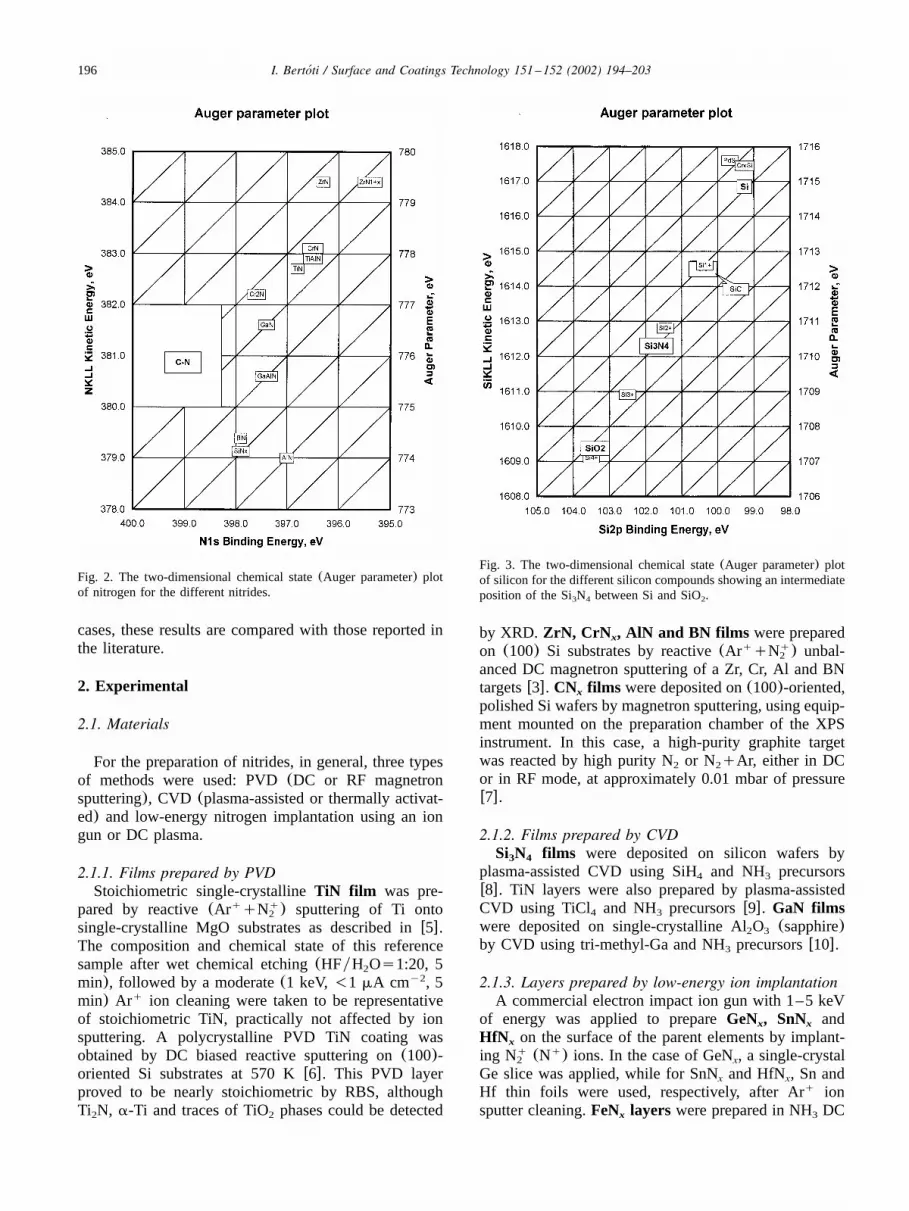
Fig. 2. The two-dimensional chemical state(Auger parameter) plotof nitrogen for the different nitrides.
Fig. 3. The two-dimensional chemical state(Auger parameter) plotof silicon for the different silicon compounds showing an intermediateposition of the Si N between Si and SiO .3 4 2
cases, these results are compared with those reported inthe literature.
2. Experimental
2.1. Materials
For the preparation of nitrides, in general, three typesof methods were used: PVD(DC or RF magnetronsputtering), CVD (plasma-assisted or thermally activat-ed) and low-energy nitrogen implantation using an iongun or DC plasma.
2.1.1. Films prepared by PVDStoichiometric single-crystallineTiN film was pre-
pared by reactive(Ar qN ) sputtering of Ti ontoq q2
single-crystalline MgO substrates as described inw5x.The composition and chemical state of this referencesample after wet chemical etching(HFyH Os1:20, 52
min), followed by a moderate(1 keV,-1 mA cm , 5y2
min) Ar ion cleaning were taken to be representativeq
of stoichiometric TiN, practically not affected by ionsputtering. A polycrystalline PVD TiN coating wasobtained by DC biased reactive sputtering on(100)-oriented Si substrates at 570 Kw6x. This PVD layerproved to be nearly stoichiometric by RBS, althoughTi N, a-Ti and traces of TiO phases could be detected2 2
by XRD. ZrN, CrN , AlN and BN films were preparedx
on (100) Si substrates by reactive(Ar qN ) unbal-q q2
anced DC magnetron sputtering of a Zr, Cr, Al and BNtargetsw3x. CN films were deposited on(100)-oriented,x
polished Si wafers by magnetron sputtering, using equip-ment mounted on the preparation chamber of the XPSinstrument. In this case, a high-purity graphite targetwas reacted by high purity N or NqAr, either in DC2 2
or in RF mode, at approximately 0.01 mbar of pressurew7x.
2.1.2. Films prepared by CVDSi N films were deposited on silicon wafers by3 4
plasma-assisted CVD using SiH and NH precursors4 3
w8x. TiN layers were also prepared by plasma-assistedCVD using TiCl and NH precursorsw9x. GaN films4 3
were deposited on single-crystalline Al O(sapphire)2 3
by CVD using tri-methyl-Ga and NH precursorsw10x.3
2.1.3. Layers prepared by low-energy ion implantationA commercial electron impact ion gun with 1–5 keV
of energy was applied to prepareGeN , SnN andx x
HfN on the surface of the parent elements by implant-x
ing N (N ) ions. In the case of GeN , a single-crystalq q2 x
Ge slice was applied, while for SnN and HfN , Sn andx x
Hf thin foils were used, respectively, after Ar ionq
sputter cleaning.FeN layers were prepared in NH DCx 3

197I. Bertoti / Surface and Coatings Technology 151 –152 (2002) 194–203´
Fig. 4. The evolution of the chemical states of N, Al and C at Ar ion depth-profiling of a plasma-nitrided Al sample.q
plasma on an ARMCO iron surface at a negative biasof y720 V with 100 mA of current, increasing thetemperature of the sample to approximately 600 K.AlNlayers were prepared on Al sheets by applying theplasma-immersion ion implantation(PIII) techniquew11,12x.
2.2. XPS and XAES analysis
2.2.1. Analysis conditionsXPS spectra were recorded on a Kratos XSAM 800
spectrometer operated in fixed retarding ratio or fixedanalyzer transmission mode using Mg Ka (1253.61,2
eV) or AlKa (1486.6 eV) excitation. The linearity of1,2
the energy scale was calibrated by the dual AlyMganode method, setting a 233.0-eV KE differencebetween the two Ag 3d lines. The pressure of the5y2
analysis chamber was lower than 10 Pa, whichy7
increased to approximately 5=10 Pa during ion bom-y5
bardment. Under these conditions, only a slow build-upof the O 1s(adsorbed CO, and H O) and C 1s(C–O2
and C–H type) signals could be detected on ion-bombarded samples. Wide-scan spectra in the 50–1250-eV kinetic energy range were recorded in 0.5-eV stepsfor all samples. Detailed spectra of the most intense
core level lines and Auger transitions of the constituentelementswmetal lines, N 1s and N(KLL )x, as well as ofthe most common impurities, oxygen and carbon(O 1sand C 1s), were recorded in 0.1-eV steps. The Augerlines and valence band were often acquired in 0.2-eVsteps. The resolution at 40 eV of pass energy, definedas the width of the Ag 3d line at half its magnitude,5y2
was 1.26 eV. At this applied resolution, the line energypositions could be determined with an accuracy equalto or better than"0.2 eV. The effective sampling depthfor these lines is approximately 8–10 nmw13x. High-energy AugerwSi(KLL ), Al(KLL )x lines excited by theBremsstrahlung part of the unmonochromatized X-rayradiation were also recorded.
2.2.2. Charge referencingSpectra of all the as-received and part of the ion-
bombarded samples were referenced to the C 1s line ofthe adventitious carbon set at 284.6 eV. The applicabilityof such referencing was proved using the gold decorationmethod by setting the Au 4f line to 84.0 eV. The7y2
position of the Ar 2p line of the implanted argon can3y2
also be used for referencing the spectra after Ar ionq
beam cleaning or during depth profiling in combinationwith Ar ion etching.q

198 I. Bertoti / Surface and Coatings Technology 151 –152 (2002) 194–203´
2.2.3. Data processingSpectra were acquired and processed by the Kratos
DS 300, DS 800 and Vision 2000 software packages.The results were severely affected by the selection ofthe background subtraction method and the width ofintegration for the doublet lines. In these experiments,both Shirley and linear-type backgrounds were applied.Quantitative analysis, based on peak area intensity, wasperformed with the XPS MultiQuant programw14x usingthe experimentally determined photo-ionization cross-section data of Evans et al.w15x and the asymmetryparameters of Reilman et al.w16x. Basic principles andexperimental approaches for the acquisition and evalu-ation of XP spectra and practical hints on the analysisof solid surfaces and thin films are described in earlyand recent monographsw13,17x.
2.2.4. Ion bombardmentAr and N ion bombardment experiments wereq q
2
performed using a Kratos MacroBeam ion gun fed withhigh-purity (5N5) gases. The ion beam(spot size ofapprox. 2 mm, non-mass-selected, incident at meanangle of 558 to the surface normal) was rastered over asample area of approximately 8=8 mm . At 2.5 keV of2
energy, a typical current density of 1–10mA ycm was2
measured as the sample current. Doses of up to 1018
ionsycm were applied. Steady-state surface alterations2
were achieved at approximately 15–30 min, i.e. withdoses at or above 10 ionsycm .17 2
3. Results and discussion
3.1. Chemical state determination
The chemical state of the nitride coatings is usuallycharacterized by the binding energy(BE) position ofthe N 1s and the respective metal or nitride-formingelement line. The Auger transitions of the nitrogen andthe metal, which can be recorded in the same experi-ment, are far less studied. This may be due to theircomplex shape, and as such, they are only occasionallyinvolved in typical analysis. The N 1s line recorded ona chemically well defined nitride is of a simple Gaussianshape with a full width at half-height of approximately1.6–1.9 eV. Any significant broadening is usually indic-ative of the presence of a new chemical state. Smallcomponents on the high BE side of the main N 1s peakare often related to various energy loss processes of theemerging photoelectrons. This is illustrated by the N 1slines for selected nitrides depicted in Fig. 1a. The N 1sBE values fall in a relatively narrow energy rangebetween 396 and 398 eV. Nitrides of Hf, Zr, Ti, Cr andFe are located in the lower BE range between 396 and397 eV. The N 1s BE for nitrides of Ge, Si, Al and Gahas values between 397 and 398 eV. The small chemicalshifts, although indicative of groups of compounds,
cannot be used alone for identification a particularnitride. It should be underlined that although the N 1sline-shapes sensitively reflect even small chemical struc-tural changes in the nitride layers, their full potentialcould not be explored due to the lack of reliablereference data. According to our experience, the bindingenergy of the N 1s line may be measurably shifted whenoxygen is also incorporated into the nitrides.The N(KLL ) Auger lines, recorded occasionally dur-
ing XPS analysis, show broader energy spread for thenitrides than the corresponding N 1s lines. A two-dimensional chemical state plot, developed by Wagnerw21x for Al and Si compounds and for other elementsw13x, was adopted in this study to characterize thechemical state of nitrogen in the nitride coatings. Theresults are shown in Fig. 2. As is evident, interstitialnitrides (ZrN, CrN, TiN) are well separated from AlN,Si N , BN and CN , possessing bonding with predomi-3 4 x
nantly covalent character.
3.1.1. Nitrides of C, Si, Al, Ga and Ge
3.1.1.1. CN . The N 1s lineshape of CN layer differsx x
significantly from those for the other nitrides shown inFig. 1a. The broad line envelope incorporates a numberof different chemical states. The similarly broad C 1ssignal supports this statement. A representative exampleof the N 1s peak generated is depicted in Fig. 1b. Thelow-energy N1 component at BE of 398.3 eV is assignedto N_C double bonds, the N2 at 400.7 eV to N–Csingle bonds and the N3 component at 400.7 eV to Nincorporated in a graphitic ring structurew18–20x. Theassignment of the N 1s(and also the related C 1s)peaks has been under debate for a long time in greatnumber of papers dealing with the characterization ofCN coatings. This latter assignment was based on ourx
experimental data obtained on N-implanted graphite,polyethylenew19x and melaminew7x, as well as on IRmeasurement of the D and G band intensity of thesefilms (being active in the IR region due to the distortedsymmetry) w20x.
3.1.1.2. Si N . The N 1s and the Si 2p line energy3 4
values are cited in Table 1. The specific feature for thisnitride, as well as for AlN, is that the high-energySi(KLL ) and Al(KLL ) lines could also be recorded andused for identification of the chemical state. The two-dimensional plot of the chemical state for Si, proposedby Wagner et al.w21x, is shown in Fig. 3. The Augerparameter values, composed of the sum of Si 2p BEqSi(KLL ) KE, can be accurately measured because theyare not affected by charge referencing. From the plot, itis obvious that the shift of the Auger line is approxi-mately two-fold that of the Si 2p line between particularchemical states. The shift in the parameter changes withthe extra-atomic relaxation energy of the Auger process

199I. Bertoti / Surface and Coatings Technology 151 –152 (2002) 194–203´
Table 1Energy position of the XPS(binding energy) and XAES(kinetic energy) spectral lines of various nitrides
Sample Present work(eV) Literature data(eV)
Nitrogen Nitride- Auger(KLL ) Nitrogen Nitride- Auger(KLL ) ReferenceN 1s forming lines N 1s forming lines
element element
CN (film)x 398.3– C 1s 284.6– N 380.0– 398.2– C 1s 284.5– w43x402.2 288.9 381.5 400.8 289.9
Si N (film)3 4 397.7 Si 2p 102.0 Si 1612.1 397.4 Si 2p 101.7 Si 1612.4 w44,21xN 379.2
SiN (impl)x 397.4 Si 2p 102.0 398.0 Si 2p 101.9 Si 1612.2 w48xGeN (impl)x 397.0 Ge 3d 30.1 397.4 Ge 2p 1218.8 w44xSnN (impl)x 396.9 Sn 3d 485.05y2
BN 397.9 B 1s 190.3 N 379.3 398.1 B 1s 190.5 N 379.2 w53xAlN 396.8 Al 2p 73.6 Al 1389.6 396.7 Al 2p 73.8 Al 1389.4 w46,47x
N 379.0 396.8 73.7 N 378.0GaN 397.4 Ga 3d 20.0 397.0 Ga 3d 20.2 w45x
Ga 2p 1117.53y2
TiN 396.7 Ti 2p 454.73y2 N 383.2 397.4 Ti 2p 455.13y2 w34,49xTiN1qx 396.7 395.8 Ti 2p 454.73y2 w39x
456.3ZrNx 396.3 Zr 3d 179.65y2 N 384.4 397.5 Zr 3d 179.85y2 w49xZrN1qx 395.4 Zr 3d 181.05y2 N 384.4HfNx 396.0 Hf 4d 211.85y2 396.6 Hf 4d 213.85y2 w50xCrN 396.5 Cr 2p 574.73y2 N 383.0 396.9 Cr 2p 574.53y2 Cr(LMM ) 489.3 w51xCr N2 397.5 Cr 2p 574.53y2 N 382.5 397.8 Cr 2p 574.53y2 Cr(LMM ) 489.1 w51xFeN (DC pl)x 397.7 Fe 2p 707.13y2 397.3 Fe 2p 706.73y2 N 383.0 w52xFeN (impl)x 396.4 Fe 2p 708.83y2
and as such, reflects the polarizability of the bondsaround the investigated Si atomw21x. Using this concept,intermediate states between the elemental silicon(Sihaving only Si neighbors) and fully oxidized silicon(Si , e.g. Si in SiO) were determined with confidence4q
2
w22,23x.When a low amount of N(-30 at.%) was implanted
into Si, one single chemical state could be identified fornitrogen accommodated among three Si neighbors, sim-ilar to its environment in the stoichiometric Si N3 4
compound. On the contrary, several states are apparentfrom the Si 2p peak envelope of silicon. This latter peakcould be deconvoluted into five components correspond-ing, in order, to Si–Si , Si–Si N, Si–Si N , Si–SiN and4 3 2 2 3
Si–N bonding states, equally separated by 0.65 eV,4
covering the 2.6-eV shift between Si and Si Nw24x.3 4
Because the XPS peak intensities are insensitive to thechemical environment, the peak areas determined in thisway reflect the relative amount of Si in the particularchemical state. Similar types of intermediate states werefound at the interface between a Si substrate and Si N3 4
film.
3.1.1.3. GeN . BE values cited in Table 1 for this systemx
are representative of a surface layer containing approx-imately 12 at.% N and 36 at.% N-bonded Ge, with theBE shifted by 0.7 eV from the remaining elemental Ge.
In accordance with the above discussion, the statescharacterized are N–Ge and Ge–Ge N.3 3
3.1.1.4. SnN . The N 1s value for SnN was obtainedx x
for 7.5 at.% implanted N. This amount of N did notcause a measurable shift of the Sn 3d line positioncompared to Sn metal.
3.1.1.5. BN films. BE values cited in Table 1 for thissystem were obtained on relatively pure PVD films withapproximately 10% oxygen impurity.
3.1.1.6. AlN films. BE values cited in Table 1 for thissystem were obtained on high-purity PVD films(O-5at.%). In addition, a layer prepared at 670 K in nitrogenplasma by PIII treatment was also characterized. Fig. 4shows the development of the N 1s, Al 2p, Al(KLL )and C 1s lines for this sample. Based on the compositiondetermined and the known chemical shifts for the Al–Nand Al–O bonding states, the intermediate peak com-ponents could be assigned to O–Al–N species, i.e. to Alatoms partly bonded to O and to Nw12x.
3.1.1.7. GaN films. The only feature to be mentioned isthat in addition to N 1s, BE values for both Ga 2p andGa 3d lines may be recorded and are reported for thegallium compounds.

200 I. Bertoti / Surface and Coatings Technology 151 –152 (2002) 194–203´
3.1.2. Nitrides of Ti, Zr, Hf, Cr and FeBE values for fairly stoichiometric compounds of
TiN, ZrN, Cr N and CrN are also cited in Table 1. For2
Ti and Zr, ‘super-stoichiometric’ TiN and ZrN1qx 1qx
compositions were also prepared and line energy valuesdetermined for these chemical sates are also included inthe table. For the case of the Fe–N system, the lineenergy values measured could not be assigned to a well-defined phase. It is interesting to note that there is asignificant, more than 1 eV shift between the N 1s linesof Cr N and CrNw25x.2
3.2. Composition, non-stoichiometry and ion beam-induced effects
3.2.1. CompositionIt is broadly documented that XPS is capable of
providing accurate analysis of the top;10 nm thicklayer of the surface of the samplew13x. The analysis isbased on the area intensity of selected peaks of theconstituent elements, normalized by the experimentallydetermined or theoretically derived differential ioniza-tion cross-sections and electron escape depths. Increasedsurface roughness and in-depth compositional inhomo-geneity may significantly affect the accuracy. Surfacecontamination, frequently apparent as thin oxide layersand hydrocarbon-type deposits, may introduce errors,especially if XPS lines involved in the analysis are wellapart in the energy scale. This effect can be eliminatedusing the XPS MultiQuant program for quantificationw14,26x. This program is also capable of evaluating thethickness of several surface layers(oxides, contami-nants, etc.) on flat, and even on structured samples.Surface segregation may also be easily detected byrecording XP spectra at different electron take-off anglesw13x.For most of the nitrides discussed in this work,
quantitative analysis can be accurately performed byXPS. An uncertainty exists for TiN connected with theintense satellite structure of the Ti 2p line and the relatedbackground subtraction procedure. It has been repeatedlydocumented that the shoulders observed on the highbinding-energy side of the Ti 2p and Ti 2p com-3y2 1y2
ponent peaks are inherent characteristic features ofstoichiometric TiN w27–33x. The concept of Strydomand Hofmannw30x was adopted by us, but applied in adifferent way, by including three loss peak doubletsw6,17,35x. Low-intensity loss peaks associated with theN 1s transition have also been included in the generationof the N 1s peak, with identical energy separation forTi 2p w6,17,35x. In general, loss peaks are characteristicfor most of the transition metal nitrides. They appear aslow intensity features on the high BE side of the spectra,not related to chemical shifts caused, e.g. by impurities.Impurities, such as oxygen(and chlorine in some
CVD samples), and adventitious carbon contamination
layers are always present on the surface of the nitridecoatings exposed to air(ambient laboratory) beforeanalysis. Although their quantity, i.e. the thickness ofsuch layers, may vary over a broad range, they areusually restricted to 1–2 nm. Such contaminant layerscan be removed by a short Ar ion sputtering usingq
moderate(f1 keV) beam energy. The nitride coatingscan readily pick up impurities during deposition, suchas oxygen and chlorine(when chlorides are used asCVD precursors), as well as carbon, due to their highchemical reactivity with these elements. The amount ofsuch impurities may be slightly overestimated by quan-titative XPS if they are not evenly distributed, butsegregated on the boundaries of nanosized grains.The importance of quantitative analysis is a trivial
fact and this has been repeatedly pointed out. This hasalso been recently shown in connection with systematicvariation of the elastic properties of TiN and TiC withx x
the N or C content of the coatingsw27x.
3.2.2. Ion beam-induced effectsIn this section, the attention of the reader is called to
some particular problems the surface analyst mayencounter in analyzing thin nitride films treated byvarious low-energy(1–5 keV) particle beams. In fact,all nitrides involved in this study were exposed to ionbombardment at certain stages of their preparation orsurface analysis. It is well known that both electronicand ballistic processes initiated by the impinging ionsmay provoke significant structural and compositionalchanges in the surface layer of the solids bombardedw17,36x. Preferential sputtering, implantation, ion beam-induced diffusion and surface segregation are citedamong the main processes leading to the alterationsobserved. For nitride coatings, these effects are notalways fully recognized. Preferential removal of nitrogenon Ar bombardment was repeatedly detected by XPSq
for a number of nitrides by the author’s groupw6,25,35x.This effect is often overlooked and false statements onthe non-preferential(congruent) sputtering of manyrefractory nitrides are published in the literature.In the following paragraphs, some representative
examples will be presented, demonstrating how theeffects of particle bombardment on the surface chemistrycan be evaluated by XPS for TiN and ZrN. Here, ourattention will be focused on an effect even less recog-nized in analysis, namely the build-up of excess nitrogenin the nitride coatings.
3.2.2.1. Effect of Ar and N ion bombardment on theq q2
PE-CVD TiN layer. The PE-CVD TiN layer was sub-jected to Ar and N bombardment in sequence. Char-q q
2
acteristic changes in the shape and intensity of the Ti2p and N 1s lines were observed. In Fig. 5a, the Ti 2plines are shown after 35 min of Ar and after successiveq

201I. Bertoti / Surface and Coatings Technology 151 –152 (2002) 194–203´
Fig. 5. Comparison of the Ti 2p(top) and the N 1s(bottom) lines ofa TiN sample after 35 min of Ar bombardment followed by 50 minq
of N bombardment.q2
Fig. 6. Comparison of the N 1s lines of a ZrN sample after 90 minof Ar bombardment followed by 40 min of N bombardment(top)q q
2
and the evolution of the concentration of the constituents at a seriesof Ar –N –Ar bombardment steps(bottom).q q q
2
50 min of N bombardment(with normalized intensity),q2
together with the difference spectrum. It is clear that akind of new doublet developed on N bombardmentq
2
with Ti 2p and Ti 2p components at approximately3y2 1y2
456.4 and 462.2 eV, respectively. Incorporation of addi-tional nitrogen and the simultaneous appearance of anew N 1s peak could be measured at this stage.Accordingly, the new doublet was assigned to Ti incor-porated into a super-stoichiometric TiN statew6x.1qx
Fig. 5b shows the change in the N 1s lineshape ofthe PE-CVD TiN sample after 35 min of Ar bombard-q
ment as compared to that after successive 50-min Nq2
bombardment. The broadening of the N 1s peak afterbombardment by N is obvious, while the main N 1sq
2
peak in TiN after Ar bombardment was found at 396.7q
eV. After N bombardment, a new peak appeared atq2
395.8 eV. The major difference between the two curvesis the high intensity of this second N 1s component ofthe N -bombarded sample. The presence of a relativelyq
2
large amount of this low-energy nitrogen in the surfacelayers of plasma-nitrided Ti samples is a characteristicfeature for the type of layers formed under high-densityN bombardment by DC plasmaw35x.q2
We observed very similar compositional(Fig. 6a) andchemical state changes(development of such a low-energy N 1s component) when bombarding a PVD ZrNcoating with N . The increase in the surface N-contentq
2
reached the level of NyZrs1.3, i.e. a compositioncorresponding to Zr N(Fig. 6b). This is in line with3 4
the results of a recent study, where Zr N was synthe-3 4
sized by plasma nitriding of a Zr filmw37x.The shift of Ti 2p to higher BE and N 1s to lower
BE can be interpreted as an increased charge transferfrom Ti to N, i.e. it can be related to the formation of acompound with ionic-type bonds. This is also in agree-ment with the 0.93-eV optical bandgap measured andthe insulating properties found for Ti N inw38x. Similar3 4
conclusions can be drawn also for the ZrN sample.There are only a few publications mentioning the
appearance of a second nitrogen peak at the lower BEside of the N 1s line, with an energy separation rangingbetween 0.9 and 1.4 eVw6,35,39–42x. Only Miyagi etal. w40x explicitly related the low BE shoulder to super-stoichiometric TiN , in full agreement with our1qx
findings.

202 I. Bertoti / Surface and Coatings Technology 151 –152 (2002) 194–203´
4. Conclusions
● XPS can be applied as a simple tool for complexcharacterization of nitride coatings.
● In addition to core level lines, Auger transitionsrecorded simultaneously can provide useful data forchemical state identification.
● Minor compositional and chemical state changes canbe detected and unambiguously interpreted, even formulti-element nanophase coatings.
● Results obtained on TiN and ZrN coatings,1qx 1qx
besides supporting earlier findings, verify the exis-tence of new compounds with more ionic Ti–N andZr–N bonds.
● Delineation of ion beam-induced stoichiometrychanges may provide valuable information for devel-oping optimum conditions for the deposition ofnitride coatings with a pre-determined compositionand structure.
Acknowledgements
This work was partially supported by HungarianNational Fund(OTKA No: T030424). Thanks are dueto M. Mohai and A. Toth for participating in XPS´experiments and discussion of the results; to Prof J.E.Sundgren(formerly at the University of Linkopping)¨and to Dr C. Mitterer, Montanuniversitat Leoben, for¨kindly providing a set of nitride coatings and to L.Gulyas for technical assistance.´
References
w1x J. Musil, Surf. Coat. Technol. 125(2000) 322.w2x S. Muhl, J.M. Mendez, Diamond Relat. Mater. 8(1999) 1809.´w3x P. Zeman, R. Cerstvy, P.H. Mayrhofer, C. Mitterer, J. Musil,´
Mater. Sci. Eng. A 289(2000) 189.w4x M.I. Lembke, D.B. Lewis, W.-D. Munz, Surf. Coat. Technol.¨
125 (2000) 263.w5x J-E. Sundgren, Doctoral Thesis�79, Linkopping University,¨
1982.w6x I. Bertoti, M. Mohai, J.L. Sullivan, S.O. Saied, Surf. Interface´
Anal. 21 (1994) 467.w7x I. Bertoti, A. Toth, M. Mohai, T. Ujvari, Surf. Interface Anal.´ ´ ´
30 (2000) 538.w8x F. Pavlyak, I. Bertoti, M. Mohai, I. Biczo, J. Giber, Surf.´ ´ ´
Interface Anal. 20(1993) 221.w9x C. Mitterer, F. Holler, F. Ustel, D. Heim, Surf. Coat. Technol.¨
125 (2000) 233.w10x B. Pecz, M.A. di Forte-Poisson, F. Huet, et al., J. Appl. Phys.´
86 (1999) 6059.w11x C. Blawert, L. Mordike, Nucl. Instrum. Methods B 127y128
(1997) 873.w12x C. Blawert, B.L. Mordike, M. Mohai, I. Bertoti, A. Juhasz, in:´ ´
J. Lendvai, T. RetiŽEds.., Proceedings of the 7th International´Seminar of IFHT on Heat Treatment and Surface Engineeringof Light Alloys, Hungarian Society of Mechanical Engineering,Budapest, 1999, p. 51.
w13x D. Briggs, M.P. Seah(Eds.), Practical Surface Analysis, JohnWiley & Sons, Chichester, 1990.
w14x M. Mohai, Surf. Interface Anal., in press.w15x S. Evans, R.G. Pritchard, J.M. Thomas, J. Electron Spectrosc.
Relat. Phenom. 14(1978) 341.w16x R.F. Reilman, A. Msezane, S.T. Manson, J. Electron Spectrosc.
Relat. Phenom. 8(1976) 389.w17x I. Bertoti, A. Toth, M. Menyhard, in: J.C. Riviere, S. Myhra´ ´ `
ŽEds.., Handbook of Surface and Interface Analysis, MarcelDekker Inc, New York, 1998, p. 297.
w18x S. Souto, M. Pickholz, M.C. dos Santos, F. Alvarez, Phys. Rev.B 57 (1998) 2536.
w19x A. Toth, T. Bell, I. Bertoti, M. Mohai, B. Zelei, Nucl. Instrum.´ ´Methods B 148(1999) 1134.
w20x T. Ujvari, A. Toth, M. Mohai, J. Szepvolgyi, I. Bertoti, Solid-´ ´ ´ ¨ ´State Ionics 141-142(2001) 65.
w21x C.D. Wagner, D.E. Passoja, H.F. Hillery, et al., J. Vac. Sci.Technol. 21(1982) 933.
w22x I. Bertoti, A. Toth, M. Mohai, R. Kelly, G. Marlettal, Nucl.´ ´Instrum. Methods B 116(1996) 200.
w23x I. Bertoti, A. Toth, M. Mohai, R. Kelly, G. Marlettal, M.´ ´Farkas-Jahnke, Nucl. Instrum. Methods B 122(1997) 510.
w24x O. Benkherourou, S. Shahnoune, M. Djabi, J.-P. Deville,Vacuum 53(1999) 427.
w25x I. Bertoti, M. Mohai, P.H. Mayrhofer, C. Mitterer, Surf.´Interface Anal., in press.
w26x M. Mohai, I. Bertoti, in: H.J. Mathieu, B. Reihl, D. Briggs´ŽEds.., ECASIA ’95, John Wiley & Sons, Chichester, 1996,p. 675.
w27x M. Guemmaz, A. Moser, J.-C. Parlebas, J. Electron Spectrosc.Relat. Phenom. 107(2000) 91.
w28x L. Porte, L. Roux, J. Hanus, Phys. Rev. B 28(1983) 3214.w29x B.J. Burrow, A.E. Morgan, R.C. Ellwanger, J. Vac. Sci. Tech-
nol. A 4 (1986) 2463.w30x I. le, R. Strydom, S. Hofmann, J. Electron Spectrosc. Relat.
Phenom. 56(1991) 85.w31x R. Bertoncello, A. Casagrande, M. Casarin, et al., Surf.
Interface Anal. 18(1992) 525.w32x C.W. Louw, I. le R. Strydom, K. van den Heever, M.J.
van Staden, Surf. Coat. Technol. 49(1991) 348.w33x I. le R. Strydom, S. Hofmann, Vacuum 41(1990) 1619.w34x B.M. Biwer, S.L. Bernasek, Surface Sci. 167(1986) 207.w35x I. Bertoti, M. Mohai, J.L. Sullivan, S.O. Saied, Appl. Surf.´
Sci. 84(1995) 357.w36x R. Kelly, I. Bertoti, A. Miotello, Nucl. Instrum. Methods B´
80y81 (1993) 1154.w37x A. Straboni, L. Pichon, T. Girardeau, Surf. Coat. Technol. 125
(2000) 100.w38x D.S. Yee, J.J. Cuomo, A.M. Frisch, D.P.E. Smith, J. Vac. Sci.
Technol. A 4(1986) 381.w39x C.G.H. Walker, S.A. Morton, N.M.D. Brown, J.A.D. Matthew,
J. Electron Spectrosc. Relat. Phenom. 95(1998) 211.w40x M. Miyagi, Y. Sato, T. Mizuno, S. Sawada, Proceedings of the
4th International Conference, Titanium ’80, The MetallurgicalSociety of AIME, Kyoto, 1980, p. 2867.
w41x K.S. Robinson, B.M.A. Sherwood, Surf. Interface Anal. 6(1984) 261.
w42x C. Ernsberger, J. Nickerson, A.E. Miller, J. Moulder, J. Vac.Sci. Technol. A 3(1985) 2415.
w43x C. Ronning, H. Feldermann, R. Merk, H. Hofsass, P. Reinke,¨J.-U. Thiele, Phys. Rev. B 58(1998) 2207.
w44x J.A. Taylor, G.M. Lancaster, J.W. Rabalais, J. Electron Spec-trosc. Relat. Phenom. 13(1978) 435.
w45x S. Anantathanasharn, S. Ootomo, T. Hasizume, H. Hasegawa,Appl. Surf. Sci. 159y160 (2000) 456.

203I. Bertoti / Surface and Coatings Technology 151 –152 (2002) 194–203´
w46x H.K. Sanghera, J.L. Sullivan, Surf. Interface Anal. 27(1999)678.
w47x N. Duez, B. Mutel, O. Dessaux, P. Goudmand, J. Grimblot,Surf. Coat. Technol. 125(2000) 79.
w48x J.A. Taylor, Appl. Surf. Sci. 7(1981) 168.w49x H. Hochst, R.D. Bringans, P. Steiner, T. Wolf, Phys. Rev. B 25¨
(1982) 7183.w50x E. Bruninx, A.F.P.M. Van Eenbergen, P. van der Werf, J.
Haisma, J. Mater. Sci. 21(1986) 541.
w51x C. Emery, A.R. Chourasia, P. Yashar, J. Electron Spectrosc.Relat. Phenom. 104(1999) 91.
w52x B.M. Biwer, S.L. Bernasek, J. Electron Spectrosc. Relat.Phenom. 40(1986) 339.
w53x C.D. Wagner, W.M. Riggs, L.E. Davis, J.F. Moulder, G.E.Muilenberg, Handbook of X-Ray Photoelectron Spectroscopy,Perkin Elmer Corporation, Physical Electronics Division, EdenPrairie, MN 55344, 1979.