Embed Size (px)
Citation preview

*This chapter has been submitted to Surf. Sci. Spectra for review (David S. Jensen, Supriya S.
Kanyal, Michael A. Vail, Andrew E. Dadson, Mark Engelhard, and Matthew R. Linford)
Chapter 9: XPS of Silicon (100)/SiO2*
9.1. Abstract
Silicon (100) substrates are ubiquitous in microfabrication and, accordingly, their surface
characteristics are important. Herein, we report the analysis of Si (100) via X-ray photoelectron
spectroscopy (XPS) using monochromatic Al Kα radiation. Survey scans show that the material
is primarily silicon and oxygen with small amounts of carbon, nitrogen, and fluorine
contamination. The Si 2p region shows two peaks that correspond to elemental silicon and
silicon dioxide. Using these peaks the thickness of the native oxide (SiO2) is estimated using the
equation of Strohmeier.1 The oxygen peak is symmetric. These silicon wafers are used as the
substrate for subsequent growth of templated carbon nanotubes in the preparation of
microfabricated thin layer chromatography plates.2-4
9.2. Introduction
Silicon wafers, especially of the (100) orientation are widely used in microfabrication and
in academic research. Accordingly, the surface characteristics of Si (100) are important. Here
XPS was used to characterize the upper ca. 10 nm of this material. The present spectra are from a
study by Jensen et al., the entirety of the study can be found in Ref 5.5 The Si (100) sample was
analyzed as received from the vendor, without any cleaning. The survey scan shows that the
material is primarily silicon and oxygen (Figure 9.1). The narrow scan of the silicon 2p region
contains two peaks (Figure 9.2) at 100.1 eV and 104.1 eV that correspond to elemental silicon
and silicon dioxide, respectively, where the upper portion of the material is the native oxide

2
layer. The thickness of the oxide layer calculated to be 1.18 ± 0.09 nm (average and standard
deviation of two measurement on two different of two different pieces of silicon) using an
equation developed by Strohmeier1, 6
and Carlson.7
{[( ⁄ ) ( ⁄ )] }
Where λSiO2 is the inelastic mean free path (IMFP or attenuation length) of the Si 2p electrons in
SiO2, θ is the photoelectron take-off angle of the analyzer,
⁄ (I corresponds to the Si
2p intensity for infinitely thick SiO2 and Si as noted in its subscript), and the ⁄ term is the
ratio of peak areas from the unknown film. The IMFP for Si 2p photoelectrons in SiO2 was taken
as 2.7 ± 0.2 nm and the value used for β was 0.83.8
The valence band portion of the spectrum from ca. 0 – 25 eV is similar to the valence
band spectra of other silicon wafers with ca. 1 nm of native oxide (Figure 9.3).9-13
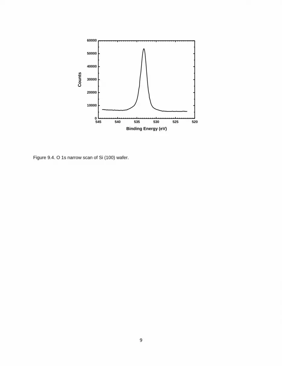
The oxygen
peak is symmetric and centered at 533.3 eV (Figure 9.4). The survey spectra show surface
contamination by fluorine, adventitious carbon, and nitrogen.
Si (100) wafers are used as the substrate for templated carbon nanotube (CNT) forests as
part of a preparation of microfabricated thin-layer chromatography plates.2-4
Indeed, submissions
to Surface Science Spectra have been made on the XPS and SIMS characterization of the key
materials in this microfabrication, Si/SiO2 (the current submission and one on ToF-SIMS14
) an
alumina barrier layer on the Si/SiO2 substrate,15, 16
the Fe film on the alumina layer,17, 18
the Fe
film after annealing in H2 to create Fe nanoparticles,19, 20
and the carbon nanotube forest grown
on the Fe nanoparticles.21, 22

3
9.3. Instrumental Parameters
XPS and valence band spectroscopy were performed on as received bare Si (100) wafers.
This work was performed at the Pacific Northwest National Laboratory (PNNL) in the
Environmental Molecular Sciences Laboratory (EMSL) using a Physical Electronics Quantera
Scanning X-ray Microprobe. This system uses a focused, monochromatic Al Kα X-ray (1486.7
eV) source for excitation, a spherical section analyzer, and a 32 element multichannel detection
system. A 98 W X-ray beam focused to 100 μm (diameter) was rastered over a 1.3 mm x 0.1 mm
rectangle on the sample. The X-ray beam is at normal incidence to the sample and the
photoelectron detector is at 45° off-normal. High energy resolution spectra were collected using
a pass-energy of 69.0 eV with a step size of 0.125 eV. For the Ag 3d5/2 line, these conditions
produced a FWHM of 1.2 eV. All samples were analyzed as received. All XPS spectra were
charge referenced to the maximum in the carbon C 1s narrow scan, taken as 285.0 eV.
9.4. Acknowledgments
We thank Diamond Analytics, a US Synthetic company (Orem, UT), for funding this
study. Part of this research was performed at EMSL, a national scientific user facility sponsored
by the Department of Energy’s Office of Biological and Environmental Research and located at
Pacific Northwest National Laboratory.
9.5. References
1. Strohmeier, B. R., Surf. Interface Anal. 1990, 15 (1), 51-56.
2. Song, J.; Jensen, D. S.; Hutchison, D. N.; Turner, B.; Wood, T.; Dadson, A.; Vail, M. A.;
Linford, M. R.; Vanfleet, R. R.; Davis, R. C., Adv. Funct. Mater. 2011, 21 (6), 1132-1139.

4
3. Jensen, D. S.; Kanyal, S. S.; Gupta, V.; Vail, M. A.; Dadson, A. E.; Engelhard, M.;
Vanfleet, R.; Davis, R. C.; Linford, M. R., J. Chromatogr., A 2012, 1257 (0), 195-203.
4. Jensen, D. S.; Kanyal, S. S.; Miles, A. J.; Davis, R. C.; Vanfleet, R.; Vail, M. A.; Dadson,
A. E.; Linford, M. R., Submitted to J. Vac. Sci. Technol., B 2012, - (-), -.
5. Jensen, D. S.; Kanyal, S. S.; Handcock, J. M.; Vail, M. A.; Dadson, A. E.;
Shutthanandan, V.; Zhu, Z.; Vanfleet, R.; Engelhard, M.; Linford, M. R., Submitted to Surf.
Interface Anal. 2012, - (-), -.
6. Lu, Z. H.; McCaffrey, J. P.; Brar, B.; Wilk, G. D.; Wallace, R. M.; Feldman, L. C.; Tay,
S. P., Appl. Phys. Lett 1997, 71 (19), 2764-2766.
7. Carlson, T. A.; McGuire, G. E., J. Electron Spectrosc. Relat. Phenom. 1972, 1 (2), 161-
168.
8. Shallenberger, J. R.; Cole, D. A.; Novak, S. W.; Moore, R. L.; Edgell, M. J.; Smith, S. P.;
Hitzman, C. J.; Kirchhoff, J. F.; Principe, E.; Biswas, S.; Bleiler, R. J.; Nieveen, W.; Jones, K. In
Oxide thickness determination by XPS, AES, SIMS, RBS and TEM, Ion Implantation Technology
Proceedings, 1998 International Conference on, 1999; 1999; pp 79-82 vol.1.
9. Zatsepin, D. A.; Mack, P.; Wright, A. E.; Schmidt, B.; Fitting, H. J., Phys. Status Solidi A
2011, 208 (7), 1658-1661.
10. van der Heide, P. A. W.; Azzarello, F. V., Surf. Sci. 2003, 531 (3), L369-L377.
11. Hirose, K.; Nohira, H.; Azuma, K.; Hattori, T., Prog. Surf. Sci. 2007, 82 (1), 3-54.
12. Hirose, K.; Nohira, H.; Koike, T.; Sakano, K.; Hattori, T., Phys. Rev. B 1999, 59 (8),
5617-5621.
13. Hirose, K.; Sakano, K.; Nohira, H.; Hattori, T., Phys. Rev. B 2001, 64 (15), 155325.
14. Kanyal, S. S.; Jensen, D. S.; Zhu, Z.; Linford, M. R., Submitted to Surf. Sci. Spectra

5
2012, - (-), -.
15. Jensen, D. S.; Kanyal, S. S.; Engelhard, M.; Linford, M. R., Submitted to Surf. Sci.
Spectra 2012, - (-), -.
16. Kanyal, S. S.; Jensen, D. S.; Zhu, Z.; Linford, M. R., Submitted to Surf. Sci. Spectra
2012, - (-), -.
17. Kanyal, S. S.; Jensen, D. S.; Zhu, Z.; Linford, M. R., Submitted to Surf. Sci. Spectra
2012, - (-), -.
18. Jensen, D. S.; Kanyal, S. S.; Engelhard, M.; Linford, M. R., Submitted to Surf. Sci.
Spectra
2012, - (-), -.
19. Kanyal, S. S.; Jensen, D. S.; Zhu, Z.; Linford, M. R., Submitted to Surf. Sci. Spectra
2012, - (-), -.
20. Jensen, D. S.; Kanyal, S. S.; Engelhard, M.; Linford, M. R., Submitted to Surf. Sci.
Spectra
2012, - (-), -.
21. Jensen, D. S.; Kanyal, S. S.; Engelhard, M.; Linford, M. R., Submitted to Surf. Sci.
Spectra
2012, - (-), -.
22. Kanyal, S. S.; Jensen, D. S.; Zhu, Z.; Linford, M. R., Submitted to Surf. Sci. Spectra
2012, - (-), -.

6
Figure 9.1. Survey scan of Si (100) wafer. O 2s (ca. 30 eV), Si 2p (ca 99 eV), 2s (ca. 150 eV), C 1s (ca. 285 eV), O 1s (ca. 530 eV), F 1s (ca. 690 eV), O KLL (ca. 975 eV), and C KVV (ca. 1230 eV).
1200 1000 800 600 400 200 00
20000
40000
60000
80000
100000
120000
Co
un
ts
Binding Energy (eV)

7
Figure 9.2. Si 2p narrow scan of Si (100) wafer. The spectrum shows peaks due to elemental Si (ca. 99 eV) and oxidized Si (ca. 104 eV).
115 110 105 100 95 900
2000
4000
6000
8000
10000
12000
14000
16000
18000
20000
Co
un
ts
Binding Energy (eV)

8
Figure 9.3. Valence band spectrum of Si (100) wafer.
25 20 15 10 5 0 -5 -100
100
200
300
400
500
600
700
800
Co
un
ts
Binding Energy
9
Figure 9.4. O 1s narrow scan of Si (100) wafer.
545 540 535 530 525 5200
10000
20000
30000
40000
50000
60000
Co
un
ts
Binding Energy (eV)


