Embed Size (px)
Citation preview

AN2016-20 Application Note Please read the Important Notice and Warnings at the end of this document <Revision 1.0>
www.infineon.com <2017-08-08>
AN2016-20 Application Note
Control Integrated POwer System (CIPOS™) PFC Integrated IPM (IFCMxxS(P)60yz) Reference Board
About this document
Scope and Purpose
The scope of this application note is to describe the product reference board-type1 of the CIPOS™ Mini PFC
integrated IPM and the basic requirements for operating the product in a recommended mode.
Environmental conditions were considered in the design of the reference board. The design was tested as described in this document but not qualified regarding safety requirements or manufacturing and operation over the whole operating temperature range or lifetime. The boards provided by Infineon are subject to functional testing only.
Reference boards are not subject to the same procedures as regular products regarding Returned Material Analysis (RMA), Process Change notification (PCN) and Product Discontinuation (PD). Reference boards are intended to be used under laboratory conditions by specialists only.
When handling or operating the board, all necessary safety precautions must be observed. The board operates at high voltages and may become hot.
Intended Audience
Power electronics engineers who want to evaluate the CIPOS™ Mini PFC integrated IPM.
Table of Contents
About this document ............................................................................................................................1
Table of Contents .................................................................................................................................1
1 Introduction ........................................................................................................................3
2 Schematic.......................................................................................................................... 4
3 External Connection ............................................................................................................5
3.1 Signal Connector ................................................................................................................................ 5
3.2 Power Terminals................................................................................................................................. 5
4 Key Parameter Setting ....................................................................................................... 6
4.1 Circuit of Input Signals (IN(xH), IN(xL)) ...............................................................................................6
4.2 Bootstrap Capacitor ...........................................................................................................................6
4.3 Internal Bootstrap Circuit Characteristics ........................................................................................... 8
4.4 Over Current Protection ..................................................................................................................... 8
4.4.1 Current Sensing Resistor Selection ................................................................................................9
4.4.2 Delay Time .................................................................................................................................. 10
4.5 Temperature Monitor and Thermal Protection ................................................................................. 10
5 PFC Control Circuit Setting ................................................................................................. 12
5.1 PFC Control Circuit in the Reference Board ...................................................................................... 12
5.2 Anti-parallel diode between collector and emitter of IGBT ............................................................... 13
5.3 PFC Control Key Parameter Setting ................................................................................................. 13
5.3.1 Gate Drive IC ............................................................................................................................... 13
5.3.2 PFC Controller ............................................................................................................................. 14

AN2016-20 Application Note 2 <Revision 1.0> <2017-08-08>
Control Integrated POwer System (CIPOS™)
CIPOS™ Mini PFC Integrated IPM (IFCMxxS(P)60yz) Reference Board-Type1
Table of Contents
5.3.3 Output Bus Voltage (DC Link Voltage) ........................................................................................ 14
5.3.4 PFC Switching Frequency ............................................................................................................ 15
5.3.5 Over Current Protection .............................................................................................................. 15
5.3.6 Gate Resistance & Capacitance for PFC IGBT .............................................................................. 16
6 Boost PFC Circuit Setting ................................................................................................... 17
6.1 Target Specification ......................................................................................................................... 17
6.2 Boost Inductor .................................................................................................................................. 17
6.3 Output Capacitor .............................................................................................................................. 18
7 Evaluation Example of Reference Board .............................................................................. 19
7.1 Evaluation Results ............................................................................................................................ 19
8 Part List............................................................................................................................ 20
9 PCB Design Guide .............................................................................................................. 22
9.1 Layout of Reference Board ............................................................................................................... 22
10 Reference ......................................................................................................................... 23
Revision History ................................................................................................................................. 23

AN2016-20 Application Note 3 <Revision 1.0> <2017-08-08>
Introduction
Control Integrated POwer System (CIPOS™)
CIPOS™ Mini PFC Integrated IPM (IFCMxxS(P)60yz) Reference Board-Type1
1 Introduction
This reference board-type1 is composed of the IFCMxxy60GD, IRS44273L (Gate driver for PFC IGBT), ICE2PCS05G (CCM PFC controller), minimum peripheral components and two current sensing resistors. It is
designed for customers to evaluate the performance of the CIPOS™ Mini PFC integrated IPM with simple
connections of 3-phase inverter control signals, PFC IGBT control signal and power wires. Figure 1 shows the external view of the reference board.
This application note also describes how to design key parameters and PCB layout.
Figure 1 Reference board pictures
12
34
56
78
910
11
12
13
14
15
16
17
18
19
20
21
22
23
24
25
26
27
28VDD VB3
VFO
ITRIP VB2
HIN1
HIN2 VB1
HIN3 HO1
LIN1 VS1
LIN2
LIN3 HO2
VS2
VSS
LO3 HO3
LO2 VS3
LO1
CIPOS™ Mini
V1
U1
Power Connectors
Signal connector to controller
Reference Board-type1
SMPSMCU
Filters & Itrip, Fo & temperature monitor
circuits
Thermistor(Optional)
P1
W1
NX1
X1
NX2
PFC controller
+
Bridge Rectifier
AC
N1
M
Boost Inductor
Shunt R (INV)
Shunt R (PFC)
Gate Driver
Figure 2 Application example

AN2016-20 Application Note 4 <Revision 1.0> <2017-08-08>
Schematic
Control Integrated POwer System (CIPOS™)
CIPOS™ Mini PFC Integrated IPM (IFCMxxS(P)60yz) Reference Board-Type1
2 Schematic
Figure 3 shows a circuitry of the reference board-type1.
The reference board consists of interface circuit, bootstrap circuit, snubber capacitors, Short Circuit (SC) protection circuit, fault output circuit, current sensing resistors, PFC gate driver and passive parts etc.
Figure 3 Circuit of the reference board
Note: The “+5V” on the CN1 HEADER 11 pin 9 denotes the control signal supply voltage such as 5V or 3.3V

AN2016-20 Application Note 5 <Revision 1.0> <2017-08-08>
External Connection
Control Integrated POwer System (CIPOS™)
CIPOS™ Mini PFC Integrated IPM (IFCMxxS(P)60yz) Reference Board-Type1
3 External Connection
3.1 Signal Connector
Table 1 Pin description of the signal connector (CN1 HEADER 11, 11-pin, 2.5mm pin pitch)
Pin No. Name Description
1 IN(UH) Control signal input for phase U upper side IGBT
2 IN(VH) Control signal input for phase V upper side IGBT
3 IN(WH) Control signal input for phase W upper side IGBT
4 IN(UL) Control signal input for phase U lower side IGBT
5 IN(VL) Control signal input for phase V lower side IGBT
6 IN(WL) Control signal input for phase W lower side IGBT
7 VFO Fault output signal
8 NC No connection
9 +5V External 5V or 3.3V supply for control signal
10 VDD External 15V supply for module and PFC controller power
11 GND Ground
3.2 Power Terminals
Table 2 Pin description of power terminals
Terminal No. Name Desctiption
NX1 NX1 Ground for DC capacitor
NX2 NX2 Ground to Bridge Diode
X1 X Inductor Input
P1 P Positive node of DC link voltage
U1 U Output node of U phase
V1 V Output node of V phase
W1 W Output node of W phase
N1 N Power Ground
AN2016-20 Application Note 6 <Revision 1.0> <2017-08-08>
Key Parameter Setting
Control Integrated POwer System (CIPOS™)
CIPOS™ Mini PFC Integrated IPM (IFCMxxS(P)60yz) Reference Board-Type1
4 Key Parameter Setting
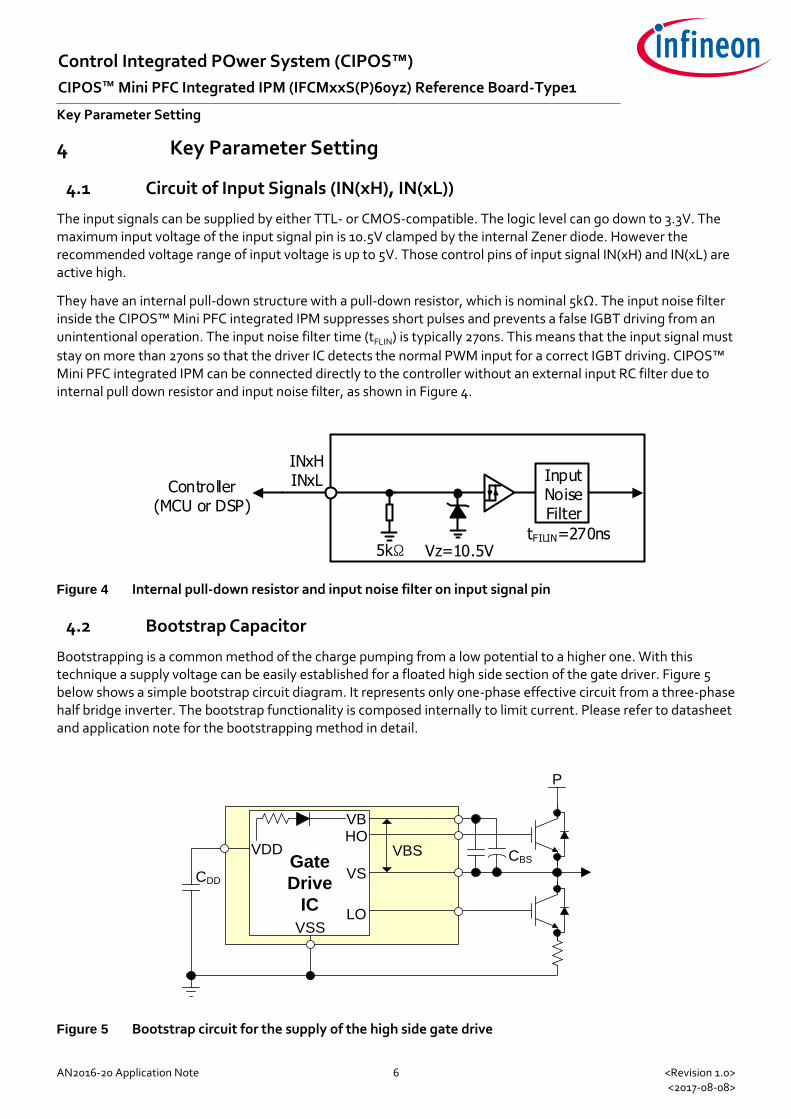
4.1 Circuit of Input Signals (IN(xH), IN(xL))
The input signals can be supplied by either TTL- or CMOS-compatible. The logic level can go down to 3.3V. The maximum input voltage of the input signal pin is 10.5V clamped by the internal Zener diode. However the recommended voltage range of input voltage is up to 5V. Those control pins of input signal IN(xH) and IN(xL) are active high.
They have an internal pull-down structure with a pull-down resistor, which is nominal 5kΩ. The input noise filter inside the CIPOS™ Mini PFC integrated IPM suppresses short pulses and prevents a false IGBT driving from an unintentional operation. The input noise filter time (tFLIN) is typically 270ns. This means that the input signal must
stay on more than 270ns so that the driver IC detects the normal PWM input for a correct IGBT driving. CIPOS™ Mini PFC integrated IPM can be connected directly to the controller without an external input RC filter due to internal pull down resistor and input noise filter, as shown in Figure 4.
InputNoiseFilter
INxHINxLController
(MCU or DSP)
tFILIN=270nsVz=10.5V5kΩ
Figure 4 Internal pull-down resistor and input noise filter on input signal pin
4.2 Bootstrap Capacitor
Bootstrapping is a common method of the charge pumping from a low potential to a higher one. With this technique a supply voltage can be easily established for a floated high side section of the gate driver. Figure 5 below shows a simple bootstrap circuit diagram. It represents only one-phase effective circuit from a three-phase half bridge inverter. The bootstrap functionality is composed internally to limit current. Please refer to datasheet and application note for the bootstrapping method in detail.
VDD
VSS
Gate
Drive
IC
P
HO
LO
CDD
CBS
VB
VS
VBS
Figure 5 Bootstrap circuit for the supply of the high side gate drive

AN2016-20 Application Note 7 <Revision 1.0> <2017-08-08>
Key Parameter Setting
Control Integrated POwer System (CIPOS™)
CIPOS™ Mini PFC Integrated IPM (IFCMxxS(P)60yz) Reference Board-Type1
A low leakage current of the high side section is very important in order to keep the bootstrap capacitor small. The bootstrap capacitor (CBS) is discharged mainly by the following mechanisms:
Quiescent current to the high side circuit in IC
Gate charge for turning high side IGBT on
Level-shift charge required by level shifters in IC
Bootstrap capacitor leakage current (can be ignored for a non-electrolytic capacitor)
Bootstrap diode leakage current
Bootstrap diode reverse recovery charge
The calculation of the bootstrap capacitor results in the following equation.
BS
Pleak BS
ΔV
tIC
Where,
CBS : bootstrap capacitor value
Ileak : maximum discharge current of the CBS
tP : maximum on pulse width of the high side IGBT
∆VBS : voltage drop at the bootstrap capacitor within a switching period
A practical leakage current level (Ileak) of the CIPOS™ Mini PFC integrated IPM is max. 1mA for 1 cycle turn on of
the HS IGBT. Figure 6 shows the curve corresponding to the CBS equation above for a continuous sinusoidal
modulation when the voltage ripple (∆VBS) is 0.1V. The recommended bootstrap capacitance for a continuous
sinusoidal modulation method is therefore in the range up to 4.7µF for 2~20kHz switching frequencies. In other PWM method case like a discontinuous sinusoidal modulation, the tP must be set to the longest period of the low
side IGBT off.
Figure 6 Value of the bootstrap capacitor as a function of the switching frequency, fPWM
0
1
2
3
4
5
0 5 10 15 20
fPWM [kHz]
CB
S [
uF
]

AN2016-20 Application Note 8 <Revision 1.0> <2017-08-08>
Key Parameter Setting
Control Integrated POwer System (CIPOS™)
CIPOS™ Mini PFC Integrated IPM (IFCMxxS(P)60yz) Reference Board-Type1
4.3 Internal Bootstrap Circuit Characteristics
CIPOS™ Mini module includes three bootstrap circuits in the internal drive IC, which consist of three diodes and
three resistors, as shown in Figure 5. A typical value of the internal bootstrap resistor is 40Ω. For more information, please refer to the below Table 3. Note that RBS2 and RBS3 have the same value with the RBS1.
Table 3 Internal bootstrap circuit characteristics
Description Condition Symbol Min. Typ. Max. Unit
Repetitive peak reverse voltage
VRRM 600 V
Bootstrap resistance of U-phase
VS2 or VS3=300V, TJ=25°C VS2 and VS3=0V, TJ=25°C VS2 or VS3=300V, TJ=125°C VS2 and VS3=0V, TJ=125°C
RBS1
35
40
50
65
Ω
Reverse recovery time IF=0.6A, di/dt=80A/µs trr_BS 50 ns
Forward voltage drop IF=20mA, VS2 and VS3=0V VF_BS 2.6 V
4.4 Over Current Protection
Over Current (OC) protection level is decided by ITRIP positive going threshold voltage (VIT,TH+) and current
sensing resistance. When the ITRIP voltage exceeds VIT,TH+, the module turns off 6 IGBTs and the fault flag is
activated during fault-output duration time, typically 65µs.
Figure 7 Timing chart of OC protection
Low Side IGBT
Collector Current
Sensing Voltage
of the shunt resistor
Fault Output Signal
SC Reference Voltage
RC circuit time
constant delay
SC
OC
Typ. 65μs Typ. 65μs
tSCP
Should set to
be within 5ms
tITRIP
HINx
LINx
HOx
LOx

AN2016-20 Application Note 9 <Revision 1.0> <2017-08-08>
Key Parameter Setting
Control Integrated POwer System (CIPOS™)
CIPOS™ Mini PFC Integrated IPM (IFCMxxS(P)60yz) Reference Board-Type1
4.4.1 Current Sensing Resistor Selection
The value of the current sensing resistor (R20) can be calculated with the following equation.
OC
TH IT,
SHI
VR
Where,
RSH : current sensing resistor value
VIT,TH+ : ITRIP positive going threshold voltage, typ. 0.47V
IOC : over current level
A maximum value of the OC protection level should be set less than the maximum peak output current in the datasheet absolute maximium ratings under considering the tolerance of the current sensing resistor.
For example, the maximum peak output current of the IFCM15P60GD is 30Apeak,
0.016Ω30A
0.47VR SH(min)
So the recommended value of the current sensing resistor should be higher than 16mΩ for IFCM15P60GD.
In order to calculate the power rating of the current sensing resistor, below items have to be taken into account.
Maximum load current of inverter (IRMS)
Shunt resistor value at TC=25°C (RSH)
Power derating ratio of the current sensing resistor at TSH=100°C according to manufacturer’s datasheet
Safety margin
And the power rating can be calculated with the equation below.
ratio Derating
marginSafety RIP SH
2
RMSSH
For example, in case of IFCM15P60GD and RSH=16mΩ,
Max. load current of inverter (IRMS) : 10ARMS
Power derating ratio of shunt resistor at TSH=100°C : 80%
Safety margin : 30%
.6W280%
130%0.01610AP
2
SH
So the proper power rating of the current sensing resistor is recommended as over than 3W.
Based on the equation, condition and calculation method above, some example values of minimum current sensing resistance and required resistor power rating are introduced as shown in below Table 4 for CIPOS™ Mini PFC integrated IPM product. When choosing a proper current sensing resistance and its power rating, an accurate OC protection level in the application set should be taken into account for a correct over current detection.

AN2016-20 Application Note 10 <Revision 1.0> <2017-08-08>
Key Parameter Setting
Control Integrated POwer System (CIPOS™)
CIPOS™ Mini PFC Integrated IPM (IFCMxxS(P)60yz) Reference Board-Type1
Table 4 Maximum peak current, shunt resistor(R20) value and required power rating
Product Max. Peak Current Min. Shunt Resistance, RSH Min. Shunt Resistance Power, PSH
IFCM10P60zD 20A 24m 1.5W
IFCM10S60zD 20A 24m 1.5W
IFCM15P60zD 30A 16m 3W
IFCM15S60zD 30A 16m 3W
4.4.2 Delay Time
RC filter should be necessary in an OC sensing circuit to prevent a false OC protection caused by noise interference. The time constant of the RC filter should be determined with considering noise period and IGBT withstanding time against the OC event. When the current flows through the current sensing resistor, the induced voltage drop on the current sensing resistor is supplied to the ITRIP pin of the CIPOS™ Mini PFC integrated IPM through the RC filter. While the ITRIP pin voltage is rising to the ITRIP positive threshold voltage (VIT,TH+ = typ. 0.47V), the filter delay time (tFilter) is created by below equation (1), (2).
𝑉𝐼𝑇,𝑇𝐻+ = 𝑅𝑆𝐻 ∙ 𝐼𝐶 ∙ (1 −1
𝑒𝑡𝐹𝑖𝑙𝑡𝑒𝑟
𝜏
) (1)
𝑡𝐹𝑖𝑙𝑡𝑒𝑟 = −𝜏 ∙ ln(1 −𝑉𝐼𝑇,𝑇𝐻+
𝑅𝑆𝐻∙𝐼𝐶) (2)
Where, VIT,TH+ is the ITRIP pin input voltage, IC is the peak current, RSH is the shunt resistor value and τ is the RC
time constant. In addition there is a shutdown propagation delay on ITRIP (tITRIP) as shown in the Table 5 below.
Table 5 Shut down propagation delay
Item Condition Min. Typ. Max. Unit
Shut down propagation delay (tITRIP)
IFCM10P60zD Iout =6A, from VIT,TH+to 10% Iout - 1290 -
ns IFCM10S60zD
IFCM15P60zD Iout =10A, from VIT,TH+to 10% Iout - 1330 -
IFCM15S60zD
Therefore, the total delay time from the occurrence of the OC event to the shut-down of the IGBT gate becomes
ITRIPFiltertotal ttt
The shut down propagation delay is in inverse proportion to the current range. Therefore the tITRIP will be shorter
with a higher current condition, comparing to the current condition in the Table 5. The total delay must be less than 5µs of the short circuit withstand time (tSC), which is specified in the datasheet. Thus, the RC time constant
should be set in the range of 1~2µs. A recommended RC filter values are 1.8kΩ R21 and 1nF C31.
4.5 Temperature Monitor and Thermal Protection
In case of the CIPOS™ Mini PFC integrated IPM, a built-in thermistor (85kΩ at 25°C) is connected between VFO and VSS pins. The typical application circuit looks like Figure 8 where the VFO pin is used for both thermistor temperature sensing and fault flag. The voltage of the VFO pin decreases as the thermistor temperature increases because the thermistor is a NTC (Negative Temperature Coefficient) type and it is connected to the external pull-up resistor. Note that the voltage variation of the VFO pin, which is generated by the thermistor temperature change, should be always higher than the fault detection level of the micro controller. In this reference board, the pull-up resistor is set to 3.6kΩ so that the VFO voltage becomes 2.95V and 1.95V

AN2016-20 Application Note 11 <Revision 1.0> <2017-08-08>
Key Parameter Setting
Control Integrated POwer System (CIPOS™)
CIPOS™ Mini PFC Integrated IPM (IFCMxxS(P)60yz) Reference Board-Type1
respectively for 5V and 3.3V control voltage (Vctr) when the thermistor temperature is 100°C, as shown in Figure 9.
IFCMxxP60zD
Drive IC
VFO
R11=3.6kΩ
Thermistor
VFO
Vctr
VSS
CIPOSTM
Input to AD Converter
Input to Fault Detection
Micro Controller
Figure 8 Temperature monitor with built in thermistor and pull up resistor
0 10 20 30 40 50 60 70 80 90 100 110 1200.0
0.5
1.0
1.5
2.0
2.5
3.0
3.5
4.0
4.5
5.0
OT set 100 : 1.95V at Vctr=3.3V
OT set 100 : 2.95V at Vctr=5V
Vctr=5V
Vctr=3.3V
VF
O [
V ]
Thermistor temperature [ oC ]
Figure 9 Voltage variation of the VFO along with the NTC thermistor temperature change

AN2016-20 Application Note 12 <Revision 1.0> <2017-08-08>
PFC Control Circuit Setting
Control Integrated POwer System (CIPOS™)
CIPOS™ Mini PFC Integrated IPM (IFCMxxS(P)60yz) Reference Board-Type1
5 PFC Control Circuit Setting
5.1 PFC Control Circuit in the Reference Board
The reference board consists of two sections for PFC integrated IPM and PFC control circuit. The PFC IGBT inside IPM needs gate drive IC for switching operation. Figure 10 shows the board configuration diagram for PFC integorated IPM and PFC control circuit section.
220V/50Hz AC Input
Rectifier
Inverter3Φ
MotorLoGateDriver COM
PFC Shunt INV. Shunt
VDC
CIPOS™ Mini PFC Integrated IPM
Reference Board-Type1MCU
Boost Inductor
PFC Controller
Figure 10 Reference board configuration diagram
Figure 11 below shows the detailed schematic of the PFC gate drive and PFC control circuit in the reference board. Infineon IRS44273L is used for the PFC gate drive and Infineon ICE2PCS05 is used for the PFC controller.
Figure 11 PFC controller and gate drive circuit for PFC IGBT

AN2016-20 Application Note 13 <Revision 1.0> <2017-08-08>
PFC Control Circuit Setting
Control Integrated POwer System (CIPOS™)
CIPOS™ Mini PFC Integrated IPM (IFCMxxS(P)60yz) Reference Board-Type1
5.2 Anti-parallel diode between collector and emitter of IGBT
In this reference board, anti-parallel diode is embedded between collector and emitter of IGBT as Figure 12. The standard conventional boost power factor correction (PFC) circuit needs this anti-parallel diode between collector and emitter of IGBT in order to prevent IGBT random failure.
X(22)
GX(24)
NX(23)
Rg
COMOUT2
VDD
IN
Diode
OUT1
VDD
Inductor
Csb1
EC
Bridge RectifierCIPOS™ Mini
R1 C1
Cf
Rf
Rshunt(PFC)
P(21)
Gate Driver
AC
PGND
SGND
2
N(17)
MCU / Controller
SGND
Figure 12 Anit-parallel diode for PFC IGBT
During startup, shutdown and under fault conditions power circuits often pass through operating modes that are not readily apparent from normal operation analysis. A PFC circuit may be designed to operate its boost inductor in the continuous current mode (CCM) during normal load operation. However, under light load, the boost inductor may go into discontinuous current mode (DCM) conduction. Discontinous operation may also occur near the AC mains zero voltage crossing even under full load conditions. Operation in DCM may require the PFC powerswitching device to conduct in the reverse direction. If an alternate current path is not provided for this switch current reversal, the IGBT may be reverse avalanched. In most cases low energy reverse avalanche is not harmful to IGBTs but it will cause additional heating. However, under specific circumstances gradual degradation and failure is possible. If the energy associated with this current reversal is minimal the failure mode may not be immediate but appear as gradual device degradation and random device failures. For detailed information, please refer to [2].
5.3 PFC Control Key Parameter Setting
5.3.1 Gate Drive IC
In order to drive the PFC (Power Factor Correction) IGBT, we strongly recommend using a gate driver IC such as IRS44273L which is a single low side driver IC. Features of IRS44273L are as below,
Features
CMOS Schmitt-triggered input
Under voltage lockout
3.3V logic compatible
1.5A Sinking / Sourcing current (typical)
50nsec Turn-on/off propagation delay (typical)

AN2016-20 Application Note 14 <Revision 1.0> <2017-08-08>
PFC Control Circuit Setting
Control Integrated POwer System (CIPOS™)
CIPOS™ Mini PFC Integrated IPM (IFCMxxS(P)60yz) Reference Board-Type1
5.3.2 PFC Controller
In order to control PFC, we recommend using a single PFC controller such as ICE2PCS05G [3] which is standalone PFC controller in CCM. Features of ICE2PCS05G are as below. For detail information about ICE2PCS05G, please refer to reference [3].
Features
Ease of Use with few External Components
Average Current Control
External Current and Voltage Loop Compensation for Greater User Flexibility
Programmable Operating/Switching Frequency (20kHz ~ 250kHz)
Trimmed Internal Reference Voltage (3V±2% at 25°C)
VCC under-Voltage Lockout,
Cycle by Cycle Peak Current Limiting
Output Over-Voltage Protection
Open Loop Detection
Short Startup(SoftStart) Duration
Fulfills Class D Requirements of IEC 61000-3-2
Soft Overcurrent Protection
5.3.3 Output Bus Voltage (DC Link Voltage)
The VSENSE pin of the PFC controller ICE2PCS05 is used for sensing the output bus voltage in order to setup the DC link voltage level. The voltage divider composed of R12~R14 senses the output bus voltage and scales it down. The scale-downed voltage by R12~R14 is supplied to the VSENSE pin. The reference voltage of the VSENSE pin is typ. 3V. The equation below shows the relationship among Vout, Vref and R12~R14..
Vout
Vref
RRR
R
1064
10
Where,
R10 : lower resistor of the voltage divider between output bus and VSENSE pin
R4+R6 : upper resistor of the voltage divider between output bus and VSENSE pin
Vref : reference voltage of the VSENSE pin, typ. 3.0V
Vout : output bus voltage (DC link voltage)
The equation above can be rearranged as below for R4+R6 calculation.
1064 RVref
VrefVoutRR
Table 1 below shows some example of R4, R6 and R10 calculation for various DC link voltages. Note that each value of R4 and R6 are a standard value based on the 5% tolerance resistors to obtain an accurate R13+R14 value.

AN2016-20 Application Note 15 <Revision 1.0> <2017-08-08>
PFC Control Circuit Setting
Control Integrated POwer System (CIPOS™)
CIPOS™ Mini PFC Integrated IPM (IFCMxxS(P)60yz) Reference Board-Type1
Table 1 Resistor value example for various DC link voltage setup
DC Link Voltage R10 R4+R6 R4 R6 Note
380V 5.9kΩ 740kΩ 180kΩ 560kΩ
390V 5.9kΩ 760kΩ 330kΩ 430kΩ
400V 5.9kΩ 780kΩ 390kΩ 390kΩ Default setting
410V 5.9kΩ 800kΩ 180kΩ 620kΩ
420V 5.9kΩ 820kΩ 200kΩ 620kΩ
5.3.4 PFC Switching Frequency
The FREQ pin is used for setting up the PFC switching frequency. A resistor value of the R9 on the FREQ pin defines the PFC switching frequency as shown in the Table 2 below. Yellow cells show default setting.
Table 2 Resistor value on FREQ pin vs. PFC switching frequency
R9 [kΩ] Fsw [kHz] R9 [kΩ] Fsw [kHz] R9 [kΩ] Fsw [kHz] R9 [kΩ] Fsw [kHz]
15 281 60 76 100 46 210 22.7
20 216 63 72 110 42 221 21.6
30 147 70 65 120 39 232 20.6
33 134 80 58 150 31.3 240 19.9
40 112 83 56 169 27.9 249 19.2
50 90 90 51 191 24.8
5.3.5 Over Current Protection
The PFC controller ICE2PCS05 has two OC protection features such as SOC (Soft Over Current Control) and PCL (Peak Current Limit).
The PFC controller IC is designed not to support any output power that corresponds to a voltage lower than typ. -0.68V at the ISENSE pin. A further increase in the inductor current, which results in a lower ISENSE voltage, will activate the SOC. It is a soft control as it does not directly switch off the gate drive. It acts on the nonlinear gain block to result in a reduced PWM duty cycle.
The PCL feature provides a cycle by cycle peak current limitation during switching. It is acvated when the voltage at ISENSE pin is lower than typ. -1.04V.
Table 3 below shows some example for setting up the OCP level with different shunt resistor values. The 30mΩ is a default shunt resistor value for PFC output current of 22.7A typ. by SOC and 34.7A typ. by PCL.
Table 3 Shunt resistor vs. OCP level for PFC control circuit
Shunt resistor R11
OCP level by SOC [A] OCP level by PCL [A] Note
Min. Typ. Max. Min. Typ. Max.
30mΩ 20.3 22.7 25.0 31.7 34.7 38.7 Default setting
40mΩ 15.3 17.0 18.8 23.8 26.0 29.0
50mΩ 12.2 13.6 15.0 19.0 20.8 23.2
The two 110Ω resistors in series (R1 and R2) are recommended in order to limit an inrush current flowing into the ISENSE pin during the power up period.

AN2016-20 Application Note 16 <Revision 1.0> <2017-08-08>
PFC Control Circuit Setting
Control Integrated POwer System (CIPOS™)
CIPOS™ Mini PFC Integrated IPM (IFCMxxS(P)60yz) Reference Board-Type1
5.3.6 Gate Resistance & Capacitance for PFC IGBT
In order to achieve low switching loss and low EMI effect, a gate resistor, R7 in the Figure 11 between gate drive IC and PFC IGBT can be used to control IGBT turn on and off speed. When decreasing the gate resistance, IGBT turn on and off speed will be getting faster and the IGBT switchinig loss will be smaller, but the EMI will be increasing by the fast dv/dt. On the contrary, increasing the gate resistance will create higher switching loss and lesser EMI. In addition, in order to prevent gate oscillation due to fast turn-on di/dt of IGBT at small Rg conditions, gate-emitter capacitance, C6 in Figure 11 between gate and emitter of IGBT is needed. A recommended gate resistance and capacitance is shown in the Table 4 below.
Table 4 Switching characteristics at recommended gate drive parameters(VDC=400V, VGE=15V, IC=15A, TJ=25°C)
Product R7 [Ω] C6 [nF] EON [μJ] On dv/dt [kV/μs]
On di/dt [A/μs]
EOFF [μJ] Off dv/dt [kV/μs]
Off di/dt [A/μs]
IFCM15P60zD 10 4.7 368 8.1 368 99 17.9 664
IFCM15S60zD 10 4.7 570 5.7 249 212 8.9 525
AN2016-20 Application Note 17 <Revision 1.0> <2017-08-08>
Boost PFC Circuit Setting
Control Integrated POwer System (CIPOS™)
CIPOS™ Mini PFC Integrated IPM (IFCMxxS(P)60yz) Reference Board-Type1
6 Boost PFC Circuit Setting
6.1 Target Specification
Table 5 below shows a target specification example for the CIPOS™ Mini PFC integrated IPM reference board.
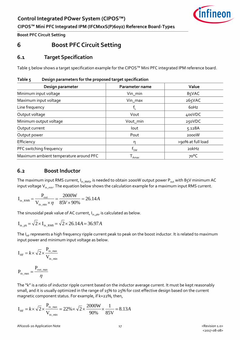
Table 5 Design parameters for the proposed target specification
Design parameter Parameter name Value
Minimum input voltage Vin_min 85VAC
Maximum input voltage Vin_max 265VAC
Line frequency fL 60Hz
Output voltage Vout 400VDC
Minimum output voltage Vout_min 250VDC
Output current Iout 5.128A
Output power Pout 2000W
Efficiency η >90% at full load
PFC switching frequency fSW 20kHz
Maximum ambient temperature around PFC TAmax 70°C
6.2 Boost Inductor
The maximum input RMS current, Iin_RMS, is needed to obtain 2000W output power Pout with 85V minimum AC
input voltage Vin_min. The equation below shows the calculation example for a maximum input RMS current.
AV
14.26%9058
2000W
V
PI
in_min
outin_RMS
The sinusoidal peak value of AC current, Iin_pk, is calculated as below.
AA 97.3614.262I2I in_RMSin_pk
The IHF represents a high frequency ripple current peak to peak on the boost inductor. It is related to maximum
input power and minimum input voltage as below.
in_min
in_max
HFV
P2I k
out_max
in_max
PP
The “k” is a ratio of inductor ripple current based on the inductor average current. It must be kept reasonably small, and it is usually optimized in the range of 15% to 25% for cost effective design based on the current magnetic component status. For example, if k=22%, then,
Ak 13.885V
1
90%
2000W2%22
V
P2I
in_min
in_max
HF

AN2016-20 Application Note 18 <Revision 1.0> <2017-08-08>
Boost PFC Circuit Setting
Control Integrated POwer System (CIPOS™)
CIPOS™ Mini PFC Integrated IPM (IFCMxxS(P)60yz) Reference Board-Type1
The peak current passing through the inductor is,
AA 04.412
8.13A97.36
2
III HF
in_peakL_pk
The on-duty of the transistor switch in a boost converter operating under CCM at minimum AC input RMS voltage is,
692.0390V
85V21
V
V21D
out
in_min
on
The boost inductor value is,
SWHF
outboost
I
VDon)-(1DonL
f
The value of Don=0.5 will generate the maximum Lboost value, so the Lboost should be selected with higher value
than below.
HkHzA
V
f600
2013.8
4000.5)-(10.5
I
VDon)-(1DonL
SWHF
out
boost
However, designer have to consider various AC input voltage conditions. For higher AC input voltage conditions as evaluation example in chapter7, we need to select bigger boost inductor value than 0.6mH@Vin=85Vac such as 2~3mH@Vin=220Vac.
The core material of the boost inductor can be either magnetic power or ferrite. For further detailed design of boost inductor, please refer to the PFC controller related or appropriate application note.[3]
6.3 Output Capacitor
An output bulk capacitor has to meet the requirement for output double line frequency ripple limit as the equation below. The Vout_ripple is normally defined as lower than 10% of Vout. For example, 3% of 400VDC Vout is around 12V of Vout_ripple. The equation below shows a calculation example of minimum output capacitance.
FVHzVf
113412602
5.128A
2
IC
out_rippleL
OUTOUT
The output capacitor of PFC circuit also has to supply enough energy to the next stage during hold-up time. The 16.7ms hold-up time is based on the line frequency of 60Hz. The output capacitor value should be higher than the result of the equation below for hold-up time requirement.
FVV
msW
VV
tP
outout
684250400
7.16200022C
222
min_
2
holdupOUT
OUT
Comparing with two output capacitor calculation values above, the 1134µF capacitor can be chosen, but a max. 20% capacitance tolerance should be considered. So, approximately 1400µF capacitor is finally recommended for the output capacitor.

AN2016-20 Application Note 19 <Revision 1.0> <2017-08-08>
Evaluation Example of Reference Board
Control Integrated POwer System (CIPOS™)
CIPOS™ Mini PFC Integrated IPM (IFCMxxS(P)60yz) Reference Board-Type1
7 Evaluation Example of Reference Board
7.1 Evaluation Results
Table 6 Evaluation Setup [DUT: IFCM15S60GD, PFC Controller: ICE2PCS05G]
Parameter Parameter name Value
PFC Part
Input Voltage Vin 220 [Vac]
Line frequency fL 60 [Hz]
PFC Switching Frequency FSW 20.0 [kHz]
Output Voltage Vout 400 [V]
Gate Resistance Rg 10 [Ω]
Gate-Emitter Capacitance Cge 4.7 [nF]
Boost Inductor LB 3.0 [mH]
Inverter Part
DC Link Voltage VDC 400 [V]
Control Supply Voltage VDD 15 [V]
Switching Frequency FSW 5 [kHz]
Power Factor P.F. 0.99
Modulation Index M.I. 0.70
Output Current IO 7.0 [Arms]
Figure 13 Operating waveform (CH1: input voltage, CH2: input current, CH3: output voltage, CH4: motor output current) and Case Temperature (TC)
Input Voltage [Vac]/Frequency [Hz]
PFC Input Current [Arms]
Input Power [kW]
Inverter Output Current [Arms]
Power Factor
THD [%]
Case Temperature [°C]
PFC IGBT Inverter IGBT
220/60 9.0 2.0 7.0 0.99 9.1 62.8 63.7
VREC.
[200 V/Div.]
IREC.
[10 A/Div.]
VDC
[200 V/Div.]
CH4: IO_U
[10 A/Div.] Time [5ms/Div.]

AN2016-20 Application Note 20 <Revision 1.0> <2017-08-08>
Part List
Control Integrated POwer System (CIPOS™)
CIPOS™ Mini PFC Integrated IPM (IFCMxxS(P)60yz) Reference Board-Type1
8 Part List
Table 7 Part list (Only for reference. Supplier can be changed)
Symbol Part description Description Part number Supplier
R1, R2, N/A (1206) Voltage divide resistor for ISENSE on PFC control(Option) N/A N/A
R3 200Ω 5% 0805 Filter resistor for PFC gate drive IC signal input WR08X201J Walsin
R4 10kΩ 5% 0805 Pull down resistor for PFC IGBT gate to emitter WR08X103J Walsin
R5 N/A (1206) Gate resistor for PFC IGBT(Option) N/A N/A
R6, R8 390kΩ 1% 1206 Voltage divide resistor for VSENSE on PFC control(Option) WR12X3903F Walsin
R7 10Ω 5% 1206 Gate resistor for PFC IGBT WR12X100J Walsin
R8 33kΩ 1% 0805 Comp. network resistor for VCOMP on PFC controller WR08X3302F Walsin
R9 240kΩ 1% 0805 Switching frequency setting resistor for PFC controller WR08X2403F Walsin
R10 5.9kΩ 1% 1206 Pull-down resistor for VSENSE on PFC controller WR12X5901F Walsin
R11 0.03 1% 5W Shunt resistor for PFC current sensing WSR5R0300F Vishay
R12~R17, R19 100Ω 5% 0805 Filter resistors for IN(xH), IN(xL), and VFO signal input WR08X101J Walsin
R18 0.03 1% 5W Shunt resistor for PFC current sensing
WSR5R0300F Vishay
R20 Refer to 4.4.1 Shunt resistor for inverter current sensing N/A Vishay
R21 1.8kΩ 1% 0805 Filter resistor for current sensing signal input WR08X1801J Walsin
C1 1nF 50V X7R 10% Filter capacitors for PFC gate drive IC signal input 0805B101K500 Walsin
C2 100μF 35V Electrolytic capacitor for 15V(VDD) supply voltage of PFC gate drive IC 100μF 35V Samyoung
C3 100nF 50V X7R 10% Decoupling capacitor for PFC gate drive IC 0805B104K500 Walsin
C4 100nF 50V X7R 10% Decoupling capacitor for PFC controller 0805B104K500 Walsin
C5 100μF 35V Electrolytic capacitor for 15V(VDD) supply voltage of PFC controller 100μF 35V Samyoung
C6 4.7nF 50V X7R 10% Filter capacitor for PFC IGBT gate to emitter 0805B471K500 Walsin
C7 10nF 50V X7R 10% Comparator network capacitor for ICOMP on PFC controller 0805B102K500 Walsin
C8 100nF 50V X7R 10% Comparator network capacitor for VCOMP on PFC controller 0805B104K500 Walsin
C9 1μF 50V X7R 10% Comparator network capacitor for VCOMP on PFC controller 0805B105K500 Walsin
C10 1μF 50V X7R 10% Filter capacitor for VSENSE on PFC controller 0805B105K500 Walsin
C11,C18,C20 22uF 35V Bootstrap capacitors for xH IGBT 22μF 35V Samyoung

AN2016-20 Application Note 21 <Revision 1.0> <2017-08-08>
Part List
Control Integrated POwer System (CIPOS™)
CIPOS™ Mini PFC Integrated IPM (IFCMxxS(P)60yz) Reference Board-Type1
Symbol Part description Description Part number Supplier
C13 100μF 35V Electrolytic capacitor for 5V supply voltage 100μF 35V Samyoung
C14 220μF 35V Electrolytic capacitor for 15V supply voltage 220μF 35V Samyoung
C16 100nF 50V X7R 10% Decoupling capacitor for 5V supply voltage 0805B104K500 Walsin
C17 100nF 50V X7R 10% Decoupling capacitor for 15V supply voltage 0805B104K500 Walsin
C19 100nF 630V 5% Snubber capacitor on inverter to reduce voltage spike
PCMP 378 J62 104
Pilkor
C22 100nF 630V 5% Snubber capacitor on inverter to reduce voltage spike
PCMP 378 J62 104
Pilkor
C23 ~ C28 1nF 50V X7R 10% Filter capacitors for IN(xH) and IN(xL) signal input 0805B101K500 Walsin
C29 1nF 50V X7R 10% Filter capacitors for VFO signal 0805B101K500 Walsin C30 1nF 50V X7R 10% Decoupling capacitors for VFO
signal 0805B101K500 Walsin C31 1nF 50V X7R 10% Filter capacitors for ITRIP signal 0805B101K500 Walsin C12,C15,C21 100nF 50V X7R 10% Bootstrap capacitors for xH IGBT 0805B104K500 Walsin D1 1N4148 Series diode for gate drive IC 1N4148 Vishay
D2 SB2K Anti-parallel diode for boost PFC SB2K Vishay CN1, CN2 SMW250-11P
11-pin connector for signal and power supply SMW250-11P Yeonho
NX1,NX2, X1, P1,U1,V1,W1,N1
Fasten Tap Power terminals GP881181-2 KET
IC2 IRS44273L Gate Drive IC for PFC IGBT IRS44273L Infineon
IPM1 N/A CIPOS™ Mini PFC integrated IPM
IFCM10P60xD IFCM10S60xD IFCM15P60xD IFCM15S60xD
Infineon

AN2016-20 Application Note 22 <Revision 1.0> <2017-08-08>
PCB Design Guide
Control Integrated POwer System (CIPOS™)
CIPOS™ Mini PFC Integrated IPM (IFCMxxS(P)60yz) Reference Board-Type1
9 PCB Design Guide
In general, there are a lot of issues to be considered when designing a 3-phase motor drives application.
Low stray inductive connection
Isolation distance
Component placement
This chapter will explain about the items above and come up with the solutions for the better layout design.
9.1 Layout of Reference Board
Figure 14 Layout of reference board type-1
1. The connection between emitters of CIPOS™ Mini PFC integrated IPM (N and NX) and current sensing resistors
should be as short and as wide as possible.
2. It is recommended that the ground pin of the micro-controller should be directly connected to the VSS pin. Signal ground and power ground should be as short as possible and connected at only one point via the VDD capacitor (C14).
3. All of the bypass capacitors should be placed as close to the pins of CIPOS™ Mini PFC integrated IPM as possible.
4. The capacitor (C31) for voltage sensing of the current sensing resistor should be placed as close to ITRIP and VSS pins as possible.
5. In order to accurately detect the voltage of the current sensing resistor, both sensing and ground patterns should be connected at the pins of the current sensing resistor and should not be overlapped with any patterns for the load current, as shown in Figure 14.
6. The snubber capacitors (C19, C22) should be placed as close to the power terminals as possible.
7. The PCB routings for power pins such as P, U, V, W, X, N and NX should be placed on both top and bottom layers with vias to allow high current flowing. They have to keep the minimum isolation distance among the power patterns. The distance should be at least over than 2.54mm.
8. Note that there are milling profiles in blue lines on the board to keep the isolation distance.
9. Make the one point connection between gate driver ground and power ground for PFC part.

AN2016-20 Application Note 23 <Revision 1.0> <2017-08-08>
Reference
Control Integrated POwer System (CIPOS™)
CIPOS™ Mini PFC Integrated IPM (IFCMxxS(P)60yz) Reference Board-Type1
10 Reference
[1] CIPOS™ Mini PFC Integrated IPM; IFCM15P60GD Datasheet
[2] AN2017-12; CIPOS Mini PFC integrated IPM technical description_V1.0_EN
[3] Design Guide for Boost Type CCM PFC with ICE2PCSxx, 2008
Revision History
Document version
Date of release Description of changes
Ver.1.0 2017.08.08 Initial Release

Edition <2017-08-08>
AN2016-20 Application Note
Published by
Infineon Technologies AG
81726 Munich, Germany
© 2017 Infineon Technologies AG. All Rights Reserved.
Do you have a question about this document?
Email: [email protected]
Document reference
IMPORTANT NOTICE The information contained in this application note is given as a hint for the implementation of the product only and shall in no event be regarded as a description or warranty of a certain functionality, condition or quality of the product. Before implementation of the product, the recipient of this application note must verify any function and other technical information given herein in the real application. Infineon Technologies hereby disclaims any and all warranties and liabilities of any kind (including without limitation warranties of non-infringement of intellectual property rights of any third party) with respect to any and all information given in this application note. The data contained in this document is exclusively intended for technically trained staff. It is the responsibility of customer’s technical departments to evaluate the suitability of the product for the intended application and the completeness of the product information given in this document with respect to such application.
For further information on the product, technology, delivery terms and conditions and prices please contact your nearest Infineon Technologies office (www.infineon.com). Please note that this product is not qualified according to the AEC Q100 or AEC Q101 documents of the Automotive Electronics Council.
WARNINGS Due to technical requirements products may contain dangerous substances. For information on the types in question please contact your nearest Infineon Technologies office. Except as otherwise explicitly approved by Infineon Technologies in a written document signed by authorized representatives of Infineon Technologies, Infineon Technologies’ products may not be used in any applications where a failure of the product or any consequences of the use thereof can reasonably be expected to result in personal injury.
Trademarks All referenced product or service names and trademarks are the property of their respective owners.