Embed Size (px)
Citation preview
Circuits and Systems Advances in N
ear Threshold Computing • Sangham
itra Roy
Circuits and Systems Advances in Near Threshold Computing
Printed Edition of the Special Issue Published in Journal of Low Power Electronics and Applications
www.mdpi.com/journal/jlpea
Sanghamitra RoyEdited by

Circuits and Systems Advances in NearThreshold Computing

Circuits and Systems Advances in NearThreshold Computing
Editor
Sanghamitra Roy
MDPI • Basel • Beijing • Wuhan • Barcelona • Belgrade • Manchester • Tokyo • Cluj • Tianjin
Editor
Sanghamitra Roy
Utah State University
USA
Editorial Office
MDPI
St. Alban-Anlage 66
4052 Basel, Switzerland
This is a reprint of articles from the Special Issue published online in the open access journal
Journal of Low Power Electronics and Applications (ISSN 2079-9268) (available at: https://www.mdpi.
com/journal/jlpea/special issues/NTC).
For citation purposes, cite each article independently as indicated on the article page online and as
indicated below:
LastName, A.A.; LastName, B.B.; LastName, C.C. Article Title. Journal Name Year, Volume Number,
Page Range.
ISBN 978-3-0365-0720-0 (Hbk)
ISBN 978-3-0365-0721-7 (PDF)
© 2021 by the authors. Articles in this book are Open Access and distributed under the Creative
Commons Attribution (CC BY) license, which allows users to download, copy and build upon
published articles, as long as the author and publisher are properly credited, which ensures maximum
dissemination and a wider impact of our publications.
The book as a whole is distributed by MDPI under the terms and conditions of the Creative Commons
license CC BY-NC-ND.
Contents
About the Editor . . . . . . . . . . . . . . . . . . . . . . . . . . . . . . . . . . . . . . . . . . . . . . vii
Preface to ”Circuits and Systems Advances in Near Threshold Computing” . . . . . . . . . . . ix
Sriram Vangal, Somnath Paul, Steven Hsu, Amit Agarwal, Ram Krishnamurthy, James Tschanz and Vivek De
Near-Threshold Voltage Design Techniques for Heterogenous Manycore System-on-ChipsReprinted from: J. Low Power Electron. Appl. 2020, 10, 16, doi:10.3390/jlpea10020016 . . . . . . . . 1
Mohammad Saber Golanbari and Mehdi Tahoori
Cross-Layer Reliability, Energy Efficiency, and Performance Optimization of Near-ThresholdData PathsReprinted from: J. Low Power Electron. Appl. 2020, 10, 42, doi:10.3390/jlpea10040042 . . . . . . . . 25
Pramesh Pandey, Noel Daniel Gundi, Prabal Basu ,Tahmoures Shabanian, Mitchell Craig Patrick, Koushik Chakraborty and Sanghamitra Roy
Challenges and Opportunities in Near-Threshold DNN Accelerators around Timing ErrorsReprinted from: J. Low Power Electron. Appl. 2020, 10, 33, doi:10.3390/jlpea10040033 . . . . . . . . 63
Alfio Di Mauro, Hamed Fatemi, Jose Pineda de Gyvez and Luca Benini
Idleness-Aware Dynamic Power Mode Selection on the i.MX 7ULP IoT Edge ProcessorReprinted from: J. Low Power Electron. Appl. 2020, 10, 19, doi:10.3390/jlpea10020019 . . . . . . . . 85
Francisco Luna-Perejon, Manuel Domınguez-Morales, Daniel Gutierrez-Galan and Anton Civit-Balcells
Low-Power Embedded System for Gait Classification Using Neural NetworksReprinted from: J. Low Power Electron. Appl. 2020, 10, 14, doi:10.3390/jlpea10020014 . . . . . . . . 93
v

About the Editor
Sanghamitra Roy is an Associate Professor in the Department of Electrical and Computer
Engineering at Utah State University. She received her Ph.D. degree in Electrical and Computer
Engineering from the University of Wisconsin-Madison. She received her M.S. degree in Computer
Engineering from Northwestern University in December 2003. Dr. Roy has authored over 80
peer-reviewed publications in top-tier journals and conferences, as well as three book chapters in VLSI
Design Automation. She serves in the editorial boards of the IEEE Design and Test Magazine and the
Journal of Low Power Electronics and Applications. She has also served in the technical program
committees of DAC, DATE, ICCAD, and ESWEEK, among others. She has received Best Paper
Award nominations at the IEEE Design Automation & Test in Europe (DATE), 2011; the IEEE/ACM
International Conference on Computer Aided Design (ICCAD), 2005; the IEEE 23rd International
Conference on VLSI Design (VLSI Design), 2010; the IEEE/ACM International Conference on
Hardware/Software Codesign and System Synthesis, 2014; and the IEEE/ACM Design Automation
and Test in Europe, March 2018. She won the Best Paper Award at the 30th IEEE International
Conference on Computer Design (ICCD), 2012. She received the NSF CAREER Award in 2013.
Her research interests are in VLSI circuit design and optimization, and exploring reliability-aware
novel circuit styles and architectures. Dr. Roy was named in the “125 People of Impact”—the list of
the most influential alumni to graduate from the University of Wisconsin-Madison—in recognition
of her ongoing success in academia and research. She is the inventor of 12 issued US patents.
vii

Preface to ”Circuits and Systems Advances in Near
Threshold Computing”
Modern society is witnessing a sea change in ubiquitous computing, in which people have
embraced computing systems as an indispensable part of day-to-day existence. Computation,
storage, and communication abilities of smartphones, for example, have undergone monumental
changes over the past decade. However, global emphasis on creating and sustaining green
environments is leading to a rapid and ongoing proliferation of edge computing systems and
applications. As a broad spectrum of healthcare, home, and transport applications shift to the edge
of the network, near-threshold computing (NTC) is emerging as one of the promising low-power
computing platforms. An NTC device sets its supply voltage close to its threshold voltage,
dramatically reducing the energy consumption. Despite showing substantial promise in terms of
energy efficiency, NTC is yet to see widescale commercial adoption. This is because circuits and
systems operating with NTC suffer from several problems, including increased sensitivity to process
variation, reliability problems, performance degradation, and security vulnerabilities, to name a few.
To realize its potential, we need designs, techniques, and solutions to overcome these challenges
associated with NTC circuits and systems. The readers of this book will be able to familiarize
themselves with recent advances in electronics systems, focusing on near-threshold computing.
Sanghamitra Roy
Editor
ix

Journal of
Low Power Electronicsand Applications
Review
Near-Threshold Voltage Design Techniques forHeterogenous Manycore System-on-Chips
Sriram Vangal *, Somnath Paul, Steven Hsu, Amit Agarwal, Ram Krishnamurthy, James Tschanz
and Vivek De
Circuit Research, Intel Labs, Intel Corporation, Hillsboro, OR 97124, USA; [email protected] (S.P.);[email protected] (S.H.); [email protected] (A.A.); [email protected] (R.K.);[email protected] (J.T.); [email protected] (V.D.)* Correspondence: [email protected]
Received: 14 April 2020; Accepted: 7 May 2020; Published: 14 May 2020
Abstract: Aggressive power supply scaling into the near-threshold voltage (NTV) region holdsgreat potential for applications with strict energy budgets, since the energy efficiency peaks as thesupply voltage approaches the threshold voltage (VT) of the CMOS transistors. The improved siliconenergy efficiency promises to fit more cores in a given power envelope. As a result, many-coreNear-threshold computing (NTC) has emerged as an attractive paradigm. Realizing energy-efficientheterogenous system on chips (SoCs) necessitates key NTV-optimized ingredients, recipes andIP blocks; including CPUs, graphic vector engines, interconnect fabrics and mm-scale microcontroller(MCU) designs. We discuss application of NTV design techniques, necessary for reliable operationover a wide supply voltage range—from nominal down to the NTV regime, and for a variety of IPs.Evaluation results spanning Intel’s 32-, 22- and 14-nm CMOS technologies across four test chips arepresented, confirming substantial energy benefits that scale well with Moore’s law.
Keywords: NTV; NTC; low-power; low-voltage memory and clocking circuits; minimum-energydesign; power-performance; resilient adaptive computing
1. Introduction
Near-threshold computing promises dramatic improvements in energy efficiency. For manyCMOS designs, the energy consumption reaches an absolute minimum in the NTV regime that isof the order of magnitude improvement over super-threshold operation [1–3]. However, frequencydegradation due to aggressive voltage scaling may not be acceptable across all single-threaded orperformance-constrained applications. The key challenge is to lock-in this excellent energy efficiencybenefit at NTV, while addressing the impacts of (a) loss in silicon frequency, (b) increased performancevariations and (c) higher functional failure rates in memory and logic circuits. Enabling digitaldesigns to operate over a wide voltage range is key to achieving the best energy efficiency [2],while satisfying varying application performance demands. To tap the full latent potential of NTC,multi-layered co-optimization approaches that crosscut architecture, devices, design, circuits, tool flowsand methodologies, and coupled with fine-grain power management techniques are mandatory torealize NTC circuits and systems in scaled CMOS process nodes.
The overarching goal of this work is to advance NTV computing, demonstrate its energy benefits,to quantify and overcome the barriers that have historically relegated ultralow-voltage operationto niche markets. We present four multi-voltage designs across three technology nodes, featuringmany-core SoC building blocks. The IPs demonstrate wide dynamic power-performance range,including reliable NTV regime operation for maximum energy efficiency. Key innovations in NTVcircuit design methods and CAD approaches for wide-dynamic range design, including optimizationsto design methodology are highlighted.
J. Low Power Electron. Appl. 2020, 10, 16; doi:10.3390/jlpea10020016 www.mdpi.com/journal/jlpea1
J. Low Power Electron. Appl. 2020, 10, 16
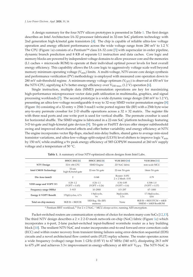
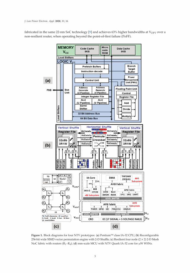
A design summary for the four NTV silicon prototypes is presented in Table 1. The first designdescribes an Intel Architecture IA-32 processor fabricated in 32-nm SoC platform technology with2nd generation high-k/metal gate transistors [4]. The chip is capable of reliable ultra-low voltageoperation and energy efficient performance across the wide voltage range from 280 mV to 1.2 V.The CPU (Figure 1a) consists of a Pentium™ class IA-32 core [5] with superscalar in-order pipeline,dynamic branch prediction and 8 KB of separate L1 instruction and data caches. Core logic andmemory blocks are powered by independent voltage domains to allow processor core and the memories(L1 caches + microcode ROM) to operate at their individual optimal power levels for best overallenergy efficiency. This capability allows the IA core logic to aggressively voltage scale well beyondmemory minimum operating voltage (Vmin) limits. A multi-voltage, NTV-aware core design synthesisand performance verification (PV) methodology is employed with measured core operation down to280 mV sub-threshold regime. A minimum-energy voltage optimum (VOPT) is observed at 450 mV forthe NTV-CPU, signifying 4.7× better energy efficiency over VDD-max (1.2 V) operation [6].
Single instruction, multiple data (SIMD) permutation operations are key for maximizinghigh-performance microprocessor vector data path utilization in multimedia, graphics, and signalprocessing workloads [7]. The second prototype is a wide dynamic range design (240 mV to 1.2 V),presenting an ultra-low-voltage reconfigurable 4-way to 32-way SIMD vector permutation engine [8](Figure 1b) consisting of a 32-entry × 256b 3-read/1-write ported register file (RF) with a 256b byte-wiseany-to-any permute crossbar for 2-D shuffle operations across a 32 × 32 matrix. The register filewith three read ports and one write port is used for vertical shuffle. The permute crossbar is usedfor horizontal shuffle. The SIMD engine is fabricated in a 22-nm SoC platform technology featuring3-D tri-gate and high-k/metal gate devices [9]. Tri-gate or FinFET devices offer steeper subthresholdswing and improved short-channel effects and offer better variability and energy efficiency at NTV.The engine incorporates vector flip-flops, stacked min-delay buffers, shared gates to average min-sizedtransistor variations, and ultra-low-voltage split-output (ULVS) level shifters to improve logic Vmin
by 150 mV, while enabling a 9× peak energy efficiency of 585 GOPS/W measured at 260 mV supplyvoltage and a temperature of 50 ◦C.
Table 1. A summary of four NTV-optimized silicon designs from Intel Labs.
ISSCC 2012 [6] ISSCC 2012 [8] VLSI 2013 [10] VLSI 2016 [11]
NTV Design 32-b ×86 CPU SIMD Engine 2D NoC fabric mm-scale MCU
Intel CMOS Technology32-nm
high-K/metal-gate 22-nm Tri-gate 22-nm Tri-gate 14nm Tri-gate
Die Area (mm2) 2 0.048 Router: 0.0512 × 2 Mesh: 0.93 0.79
VDD range and VOPT (V)0.28–1.2
(VOPT = 0.45)0.24–1.1
(VOPT = 0.26)0.34–0.85
(VOPT = 0.4)0.308–1.0
(VOPT = 0.37)
Frequency range (MHz) 3–915 10–2900 0.5–297 67–1000
Energy @ VOPT Benefit 170pJ/cyclea, 4.7× 1.9pJ/cycle,9×
36pJ/cycleb,3.3×
17.18pJ/cyclec,4.8×
Total on-chip memory 8KB I$ + 8KB D$ 1KB Reg. file (RF)memory None 8KB I$ + 8KB DTCM + 64KB
SMEM + 16KB BootROMa Pentium BIST workload, b For 2 × 2 NoC, c MCU always-active, running AES encryption.
Packet-switched routers are communication systems of choice for modern many-core SoCs [12,13].The third NTV design describes a 2 × 2 2-D mesh network-on-chip (NoC) fabric (Figure 1c) whichincorporates a 6-port, 2-lane packet-switched input-buffered wormhole router as a key buildingblock [10]. The resilient NTV-NoC and router incorporates end-to-end forward error correction code(ECC) and within router recovery from transient timing failures using error-detection sequential (EDS)circuits and a novel architectural flow control units (FLIT) replay scheme. The router operates acrossa wide frequency (voltage) range from 1 GHz (0.85 V) to 67 MHz (340 mV), dissipating 28.5 mWto 675 μW and achieves 3.3× improvement in energy-efficiency at 400 mV VOPT. The NTV-NoC is
2
J. Low Power Electron. Appl. 2020, 10, 16
fabricated in the same 22-nm SoC technology [9] and achieves 63% higher bandwidths at VOPT over anon-resilient router, when operating beyond the point-of-first failure (PoFF).
Figure 1. Block diagrams for four NTV prototypes: (a) Pentium™ class IA-32 CPU; (b) Reconfigurable256-bit wide SIMD vector permutation engine with 2-D Shuffle; (c) Resilient four node (2 × 2) 2-D MeshNoC fabric with routers (R1–R4); (d) mm-scale MCU with NTV Quark IA-32 core for μW WSNs.
3
J. Low Power Electron. Appl. 2020, 10, 16
The final NTV prototype showcases a wireless sensor node (WSN) platform that integrates amm-scale, 0.79 mm2 NTV IA-32 Quark™microcontroller (Figure 1d) (MCU) [14,15], built using a 14-nm2nd generation tri-gate CMOS process. The WSN platform includes a solar cell, energy harvester, flashmemory, sensors and a Bluetooth Low Energy (BLE) radio, to enable always-on always-sensing (AOAS)and advanced edge computing capabilities in Internet-of-Things (IoT) systems [11]. The MCU featuresfour independent voltage-frequency islands (VFI), a low-leakage SRAM array, an on-die oscillator clocksource capable of operating at sub-threshold voltage, power-gating and multiple active/sleep states,managed by an integrated power management unit (PMU). The MCU operates across a wide frequency(voltage) range of 297 MHz (1 V) to 0.5 MHz (308 mV) and achieves 4.8× improvement in energyefficiency at an optimum supply voltage (VOPT) of 370 mV, operating at 3.5 MHz. The WSN, powered bya solar cell, demonstrates sustained MHz AOAS operation, consuming only 360 μW.
This paper is organized as follows: Section 2 describes various NTV design techniques for SRAMand logic circuits. Architecture driven adaptive mechanisms to address higher functional failure ratesand variation-tolerant resiliency at NTV for SoC fabrics are described in Section 3. Section 4 presentsthe tools, flows and recipes for wide-dynamic range design. In addition, solutions for multi-voltageglobal clock generation and distribution are introduced. Key experimental results from measuring allfour prototypes are presented, analyzed, and discussed in Section 5. Finally, Section 6 concludes thepaper and suggests future work.
2. NTV Circuit Design Methodology
The most common limit to voltage scaling is failure of SRAM and logic circuits. SRAM cells fail atlow voltage because device mismatches degrade stability of the bit-cell for read, write or data retention.SRAM cells typically use the smallest transistors. Also, they are the most abundant among all circuittypes on a die. Therefore, the Vmin of the SRAM cell array limits Vmin of the entire chip. Logic circuits,clocking, and sequentials fail at low voltage because of noise and process variations. Alpha and cosmicray-induced soft errors cause transient failure of memory, sequentials, and logic at NTV. Frequencystarts degrading exponentially as the supply voltage approaches VT. This sets a limit on Vmin. This limitcan be alleviated to some extent by tri-gate transistors. Since they have a steeper sub-threshold swing,they can provide a lower VT for the same leakage current target. Aging degradations cause failureof SRAM cells at low voltages since different transistors in the cell undergo different amounts of VT
shift under voltage–temperature stress and thus worsen device mismatches in the bit-cells. All theseeffects degrade and limit Vmin. The following sections describe low-voltage design techniques used forSRAM memory, combinational cells, sequentials and voltage level shifters circuits.
2.1. SRAM Memory and Register File (RF) Optimizations
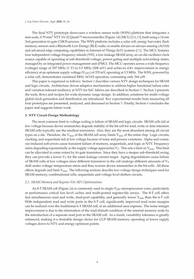
An 8-T SRAM cell (Figure 2a) is commonly used in single-VDD microprocessor cores, particularlyin performance critical low-level caches and multi-ported register-file arrays. The 8-T cell offersfast simultaneous read and write, dual-port capability, and generally lower Vmin than the 6-T cell.With independent read and write ports in the 8-T cell, significantly improved read noise marginscan be realized over the traditional 6-T SRAM cell, at an additional area expense. The noise marginimprovement is due to the elimination of the read-disturb condition of the internal memory node bythe introduction of a separate read port in the SRAM cell. As a result, variability tolerance is greatlyenhanced, making it a desirable design choice for ULP SRAM memory operating at lower supplyvoltages down to NTV and energy-optimum points.
4
J. Low Power Electron. Appl. 2020, 10, 16
Figure 2. The prototypes use variability-tolerant SRAM bit-cells: (a) 8-T SRAM bit-cell used in theNTV-MCU; (b) The SIMD engine uses a 10-T dual-ended transmission gate (DETG) SRAM topology;(c) An alternate 10-T transmission gate (TG) SRAM bit-cell used in the NTV-CPU; (d) Simulatedretention voltage simulations for the 10-T TG SRAM in 32-nm, as a function of keeper device size(m9, m10) in the presence of random variations (5.9σ, slow skew, −25 ◦C); (e) The shared PMOS/NMOSon the virtual supplies improve memory write Vmin by 125 mV in the 22-nm DETG based memory array.
The 8-T bit-cell is still prone to write failures due to write contention between strong PMOSpull-up and a weak NMOS transfer device across PVT variation. This contention becomes worseas VDD is lowered, limiting Vmin. A variation-tolerant dual-ended transmission gate (DETG) cell isimplemented on the 22-nm NTV-SIMD register file array by replacing the NMOS transfer devices withfull transmission gates (Figure 2b). This design enables a strong “1” and “0” write on both sides of thecross-coupled inverter pair. The DETG cell always has two NMOS or two PMOS devices to write a “1”or “0”, on nodes bit and bitx. This inherent redundancy averages the random variation effect acrossthe transistors, improving both contention and write-completion. Moreover, the cell is symmetricwith respect to PMOS and NMOS skew which reduces the effect of systematic variation. DETG cellsimulations show 24% improvement in write delay, allowing a 150 mV reduction in write Vmin.However, the DETG cell is contention limited at its write Vmin, which can be reduced by the shared
5
J. Low Power Electron. Appl. 2020, 10, 16
P/N circuits. An always “ON” PMOS and NMOS is shared across the virtual supplies of eight DETGcells (Figure 2e). The shared P/N circuit limits the strength of the cross-coupled inverters acrossvariations reducing write contention by 22%. This circuit optimization results in an additional 125 mVwrite reduction compared to DETG, enabling an overall 275 mV write Vmin reduction when comparedto the 8-T SRAM cell.
Caches in the 32-nm NTV-CPU use a modified, single-ended and fully interruptible 10-Ttransmission gate (TG) SRAM bit-cell (Figure 2c), which allows for contention-free write operations.This topology enables a 250 mV improvement in write Vmin over an 8-T bit-cell. With this improvement,bit-cell retention now becomes a key VDD limiter. The simulated retention voltage data for the 10-TTG SRAM, as a function of keeper device size (m9, m10) and in the presence of random variations(5.9σ, slow skew, −25 ◦C) is shown in Figure 2d. Clearly, larger keeper devices lower the retentionvoltage. The keeper device is increased from 140-nm to 200-nm to realize a 550 mV retention Vmin
target. For reliable read operation, bit-lines incorporate a scan-controlled, programmable stackedkeeper, which can be configured to three or four PMOS device stacks to reduce read contention andimprove read Vmin, across wide operating voltage/frequency range.
To achieve low standby power in the WSN, all on-die memories and caches on the 14-nmNTV-MCU use a custom 8-T (Figure 2a), 0.155-μm2 bit-cell, built using 84-nm gate pitch ultra-lowpower (ULP) transistors [14]. The 8-T bit-cell provides a well-balanced trade-off in Vmin and area overthe 6-T and 10-T SRAM cells. The ULP transistor optimized memory arrays are designed to providelow standby leakage. However, as summarized in Table 2, a 5× performance slowdown is estimatedover standard performance (SP) transistor 8T memory at 500 mV, but is still fast enough for edgecompute applications. Context-aware power-gating of each 2 KB array is supported for further leakagereduction with no state retention. The ULP array also enables 26× lower leakage (at 500 mV supply)and has a 55% area cost over an SP-based 8T memory array, drawn on a 70 nm gate pitch. The ULPmemory leakage scales from 114 pA at 1 V voltage down to 8.28 pA per bit at the retention limit of308 mV, as measured at room temperature (25 ◦C).
Table 2. Comparison between 8T SRAMS build with ULP and SP bit-cells.
8T SRAM Device Type. Gate PitchNormalized
Frequency (0.5V)Normalized Leakage
(0.5V, 25C)14 nm Bit-Cell
Area (μm2)
Standard performance (SP) 70nm 5× 26× 0.100 μm2
Ultralow power (ULP, NTVMCU Memory) 84nm 1× 1× 0.155 μm2 (1.55×)
Process, voltage and temperature (PVT) and aging adaptive on-die boosting of read word-line(RWL) and write word-line (WWL) as a common circuit assist technique for further lowering SRAMVmin is described in [16,17]. Boosting RWL enables larger read “ON” current without forcing a largerPMOS keeper. Boosting WWL helps write Vmin for two reasons—it improves contention withoutupsizing NMOS pass device size (or lowering its VTH), and improving write completion by writing a “1”from the other side. At iso-array area, on-die WL boosting achieves twice as much Vmin reduction overbit- cell upsizing [16]. However, word-line boosting requires an integrated charge-pump, or anothermethod for generating a boosted voltage on die.
2.2. Combinational Cells Design Criteria
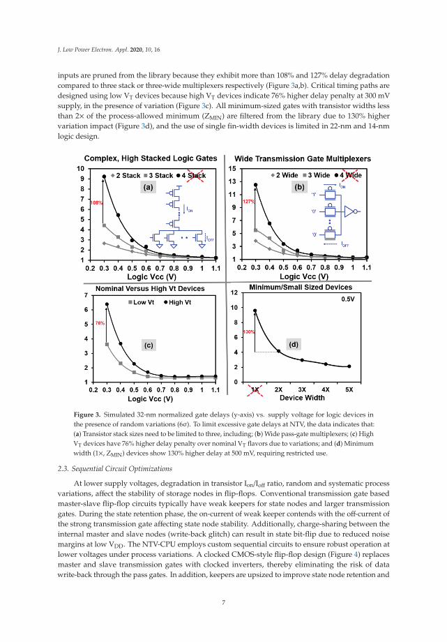
Circuits are optimized for robust and reliable ultra-low voltage operation. A variation-awarepruning is performed on the standard cell library to eliminate the circuits which exhibit DC failuresor extreme delay degradation at NTV due to reduced transistor on/off current ratios and increasedsensitivity to process variations. Simulated 32-nm normalized gate delays (y-axis), as a function ofVDD for logic devices in the presence of random variations (6σ) is presented in Figure 3. Complex logicgates with four or more stacked devices and wide transmission-gate multiplexers with four or more
6
J. Low Power Electron. Appl. 2020, 10, 16
inputs are pruned from the library because they exhibit more than 108% and 127% delay degradationcompared to three stack or three-wide multiplexers respectively (Figure 3a,b). Critical timing paths aredesigned using low VT devices because high VT devices indicate 76% higher delay penalty at 300 mVsupply, in the presence of variation (Figure 3c). All minimum-sized gates with transistor widths lessthan 2× of the process-allowed minimum (ZMIN) are filtered from the library due to 130% highervariation impact (Figure 3d), and the use of single fin-width devices is limited in 22-nm and 14-nmlogic design.
Figure 3. Simulated 32-nm normalized gate delays (y-axis) vs. supply voltage for logic devices inthe presence of random variations (6σ). To limit excessive gate delays at NTV, the data indicates that:(a) Transistor stack sizes need to be limited to three, including; (b) Wide pass-gate multiplexers; (c) HighVT devices have 76% higher delay penalty over nominal VT flavors due to variations; and (d) Minimumwidth (1×, ZMIN) devices show 130% higher delay at 500 mV, requiring restricted use.
2.3. Sequential Circuit Optimizations
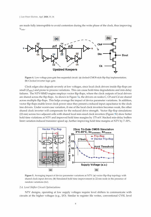
At lower supply voltages, degradation in transistor Ion/Ioff ratio, random and systematic processvariations, affect the stability of storage nodes in flip-flops. Conventional transmission gate basedmaster-slave flip-flop circuits typically have weak keepers for state nodes and larger transmissiongates. During the state retention phase, the on-current of weak keeper contends with the off-current ofthe strong transmission gate affecting state node stability. Additionally, charge-sharing between theinternal master and slave nodes (write-back glitch) can result in state bit-flip due to reduced noisemargins at low VDD. The NTV-CPU employs custom sequential circuits to ensure robust operation atlower voltages under process variations. A clocked CMOS-style flip-flop design (Figure 4) replacesmaster and slave transmission gates with clocked inverters, thereby eliminating the risk of datawrite-back through the pass gates. In addition, keepers are upsized to improve state node retention and
7
J. Low Power Electron. Appl. 2020, 10, 16
are made fully interruptible to avoid contention during the write phase of the clock, thus improvingVmin.
Figure 4. Low-voltage pass-gate free sequential circuit: (a) clocked-CMOS-style flip-flop implementation;(b) Clocked inverter logic gate.
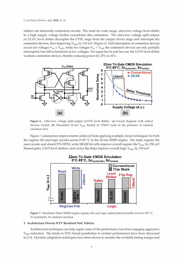
Clock edges also degrade severely at low voltages, since local clock drivers inside flip-flops aresmall (ZMIN) and prone to process variations. This can cause hold-time degradations and min-delayfailures. The NTV-SIMD engine employs vector flip-flops, where the clock outputs of local driversare shared across the flip-flops. As shown in Figure 5a, the drivers on nodes C, C# and Cd are sharedacross multiple flip-flops. This helps average the impact of device parameter variations. In addition,vector flip-flops enable lower clock power since they present a reduced input capacitance to the clocktree drivers. Under worst-case variation, if one of the local clock inverters becomes weak, the othershared clock inverter will compensate for the reduced drive strength. Vector flip-flop simulations(22-nm) across two adjacent cells with shared local min-sized clock inverters (Figure 5b) show betterhold time violations at NTV and improved hold time margins by 175 mV. Stacked min-delay bufferslimit variation-induced transistor speed up, further improving hold time margins at NTV by 7–30%.
Figure 5. Averaging impact of device parameter variations at NTV: (a) vector flip-flop topology withshared clock input drivers; (b) Simulated hold time improvement in 22-nm node in the presence ofrandom variations (6σ).
2.4. Level Shifter Circuit Optimizations
NTV designs, operating at low supply voltages require level shifters to communicate withcircuits at the higher voltages (e.g., I/O). Similar to register file writes, conventional CVSL level
8
J. Low Power Electron. Appl. 2020, 10, 16
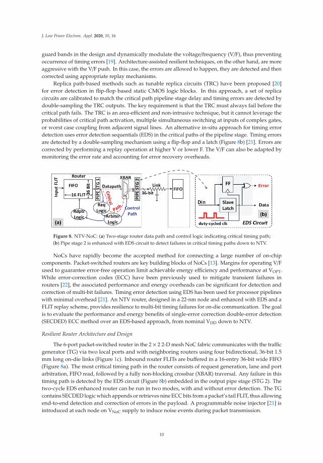
shifters are inherently contention circuits. The need for wide range, ultra-low voltage level shifterto a high supply voltage further exacerbates this contention. The ultra-low voltage split-output,or ULVS, level shifter decouples the CVSL stage from the output driver stage and interrupts thecontention devices, thus improving Vmin by 125 mV (Figure 6). Full interruption of contention devicesoccurs for voltages Vin ≥ Vout, while for voltages Vin < Vout the contention devices are only partiallyinterrupted, but still is beneficial at low voltages. For equal fan-in and fan-out, the ULVS level shifterweakens contention devices, thereby reducing power by 25% to 32%.
Figure 6. Ultra-low voltage split-output (ULVS) level shifter: (a) Circuit diagram with criticaldevices circled; (b) Simulated 22-nm Vmin benefit of 125mV node in the presence of randomvariations (6σ).
Figure 7 summarizes improvements achieved from applying multiple circuit techniques for boththe register file and logic circuits across 0–85 ◦C in the 22-nm SIMD engine. The static register fileread circuits and shared P/N DETG write SRAM bit-cells improve overall register file Vmin by 250 mV.Shared gates, ULVS level shifters, and vector flip-flops improve overall logic Vmin by 150 mV.
Figure 7. Simulated 22nm SIMD engine register file and logic optimization benefits across 0–85 ◦C,3σ systematic, 6σ random variation.
3. Architecture Driven NTV Resilient NoC Fabrics
Architectural techniques can help regain some of the performance loss from engaging aggressiveVDD reduction. The limits to NTC-based parallelism to reclaim performance have been discussedin [18]. Dynamic adaptation techniques have been shown to monitor the available timing margin and
9
J. Low Power Electron. Appl. 2020, 10, 16
guard bands in the design and dynamically modulate the voltage/frequency (V/F), thus preventingoccurrence of timing errors [19]. Architecture-assisted resilient techniques, on the other hand, are moreaggressive with the V/F push. In this case, the errors are allowed to happen, they are detected and thencorrected using appropriate replay mechanisms.
Replica path-based methods such as tunable replica circuits (TRC) have been proposed [20]for error detection in flip-flop based static CMOS logic blocks. In this approach, a set of replicacircuits are calibrated to match the critical path pipeline stage delay and timing errors are detected bydouble-sampling the TRC outputs. The key requirement is that the TRC must always fail before thecritical path fails. The TRC is an area-efficient and non-intrusive technique, but it cannot leverage theprobabilities of critical path activation, multiple simultaneous switching at inputs of complex gates,or worst case coupling from adjacent signal lines. An alternative in-situ approach for timing errordetection uses error detection sequentials (EDS) in the critical paths of the pipeline stage. Timing errorsare detected by a double-sampling mechanism using a flip-flop and a latch (Figure 8b) [21]. Errors arecorrected by performing a replay operation at higher V or lower F. The V/F can also be adapted bymonitoring the error rate and accounting for error recovery overheads.
Figure 8. NTV-NoC: (a) Two-stage router data path and control logic indicating critical timing path;(b) Pipe stage 2 is enhanced with EDS circuit to detect failures in critical timing paths down to NTV.
NoCs have rapidly become the accepted method for connecting a large number of on-chipcomponents. Packet-switched routers are key building blocks of NoCs [13]. Margins for operating V/Fused to guarantee error-free operation limit achievable energy efficiency and performance at VOPT.While error-correction codes (ECC) have been previously used to mitigate transient failures inrouters [22], the associated performance and energy overheads can be significant for detection andcorrection of multi-bit failures. Timing error detection using EDS has been used for processor pipelineswith minimal overhead [21]. An NTV router, designed in a 22-nm node and enhanced with EDS and aFLIT replay scheme, provides resilience to multi-bit timing failures for on-die communication. The goalis to evaluate the performance and energy benefits of single-error correction double-error detection(SECDED) ECC method over an EDS-based approach, from nominal VDD down to NTV.
Resilient Router Architecture and Design
The 6-port packet-switched router in the 2 × 2 2-D mesh NoC fabric communicates with the trafficgenerator (TG) via two local ports and with neighboring routers using four bidirectional, 36-bit 1.5mm long on-die links (Figure 1c). Inbound router FLITs are buffered in a 16-entry 36-bit wide FIFO(Figure 8a). The most critical timing path in the router consists of request generation, lane and portarbitration, FIFO read, followed by a fully non-blocking crossbar (XBAR) traversal. Any failure in thistiming path is detected by the EDS circuit (Figure 8b) embedded in the output pipe stage (STG 2). Thetwo-cycle EDS enhanced router can be run in two modes, with and without error detection. The TGcontains SECDED logic which appends or retrieves nine ECC bits from a packet’s tail FLIT, thus allowingend-to-end detection and correction of errors in the payload. A programmable noise injector [21] isintroduced at each node on VNoC supply to induce noise events during packet transmission.
10
J. Low Power Electron. Appl. 2020, 10, 16
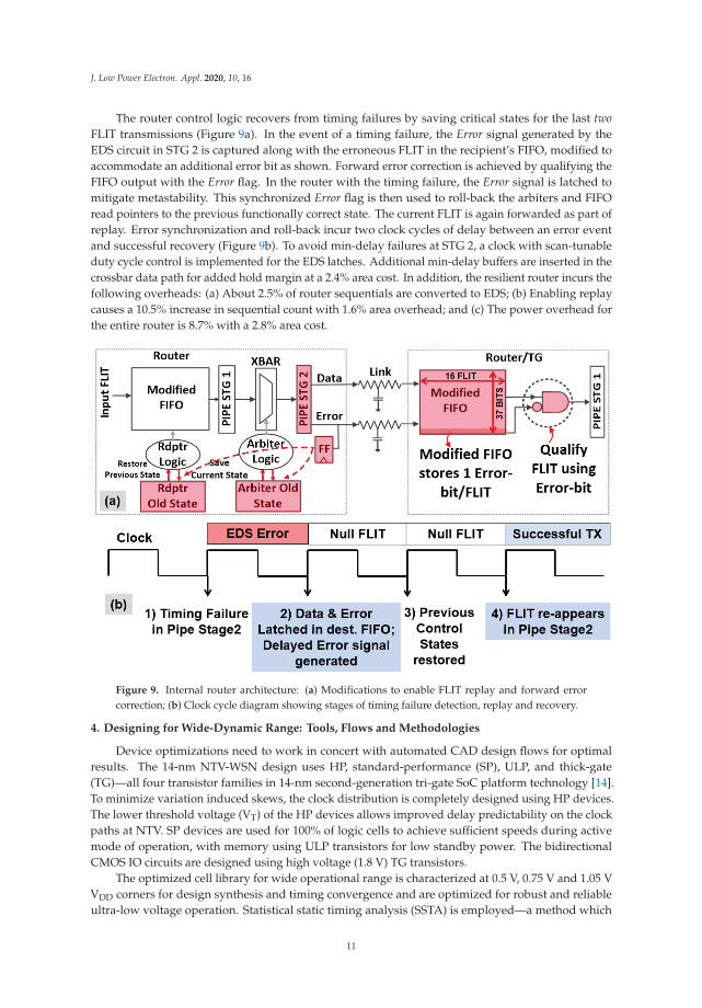
The router control logic recovers from timing failures by saving critical states for the last twoFLIT transmissions (Figure 9a). In the event of a timing failure, the Error signal generated by theEDS circuit in STG 2 is captured along with the erroneous FLIT in the recipient’s FIFO, modified toaccommodate an additional error bit as shown. Forward error correction is achieved by qualifying theFIFO output with the Error flag. In the router with the timing failure, the Error signal is latched tomitigate metastability. This synchronized Error flag is then used to roll-back the arbiters and FIFOread pointers to the previous functionally correct state. The current FLIT is again forwarded as part ofreplay. Error synchronization and roll-back incur two clock cycles of delay between an error eventand successful recovery (Figure 9b). To avoid min-delay failures at STG 2, a clock with scan-tunableduty cycle control is implemented for the EDS latches. Additional min-delay buffers are inserted in thecrossbar data path for added hold margin at a 2.4% area cost. In addition, the resilient router incurs thefollowing overheads: (a) About 2.5% of router sequentials are converted to EDS; (b) Enabling replaycauses a 10.5% increase in sequential count with 1.6% area overhead; and (c) The power overhead forthe entire router is 8.7% with a 2.8% area cost.
Figure 9. Internal router architecture: (a) Modifications to enable FLIT replay and forward errorcorrection; (b) Clock cycle diagram showing stages of timing failure detection, replay and recovery.
4. Designing for Wide-Dynamic Range: Tools, Flows and Methodologies
Device optimizations need to work in concert with automated CAD design flows for optimalresults. The 14-nm NTV-WSN design uses HP, standard-performance (SP), ULP, and thick-gate(TG)—all four transistor families in 14-nm second-generation tri-gate SoC platform technology [14].To minimize variation induced skews, the clock distribution is completely designed using HP devices.The lower threshold voltage (VT) of the HP devices allows improved delay predictability on the clockpaths at NTV. SP devices are used for 100% of logic cells to achieve sufficient speeds during activemode of operation, with memory using ULP transistors for low standby power. The bidirectionalCMOS IO circuits are designed using high voltage (1.8 V) TG transistors.
The optimized cell library for wide operational range is characterized at 0.5 V, 0.75 V and 1.05 VVDD corners for design synthesis and timing convergence and are optimized for robust and reliableultra-low voltage operation. Statistical static timing analysis (SSTA) is employed—a method which
11
J. Low Power Electron. Appl. 2020, 10, 16
replaces the normal deterministic timing of gates and interconnects with probability distributions andprovides a distribution of possible circuit outcomes [23,24]. As discussed in Section 2.2, variation-awareSSTA study is performed on the standard cell library to eliminate the circuits which exhibit DC failuresor extreme delay degradation due to reduced transistor on/off current ratios and increased sensitivityto process variations. As a result, the standard cell library was conservatively constrained for use inthe NTV optimized designs.
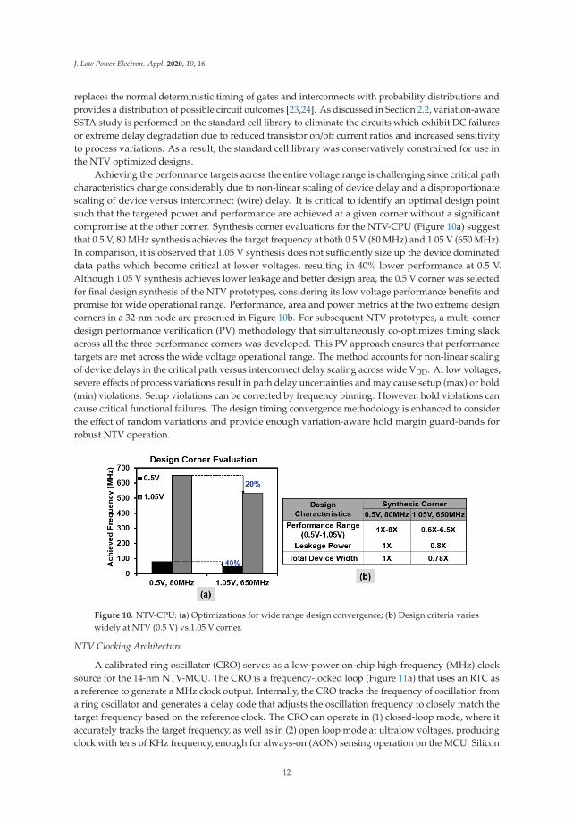
Achieving the performance targets across the entire voltage range is challenging since critical pathcharacteristics change considerably due to non-linear scaling of device delay and a disproportionatescaling of device versus interconnect (wire) delay. It is critical to identify an optimal design pointsuch that the targeted power and performance are achieved at a given corner without a significantcompromise at the other corner. Synthesis corner evaluations for the NTV-CPU (Figure 10a) suggestthat 0.5 V, 80 MHz synthesis achieves the target frequency at both 0.5 V (80 MHz) and 1.05 V (650 MHz).In comparison, it is observed that 1.05 V synthesis does not sufficiently size up the device dominateddata paths which become critical at lower voltages, resulting in 40% lower performance at 0.5 V.Although 1.05 V synthesis achieves lower leakage and better design area, the 0.5 V corner was selectedfor final design synthesis of the NTV prototypes, considering its low voltage performance benefits andpromise for wide operational range. Performance, area and power metrics at the two extreme designcorners in a 32-nm node are presented in Figure 10b. For subsequent NTV prototypes, a multi-cornerdesign performance verification (PV) methodology that simultaneously co-optimizes timing slackacross all the three performance corners was developed. This PV approach ensures that performancetargets are met across the wide voltage operational range. The method accounts for non-linear scalingof device delays in the critical path versus interconnect delay scaling across wide VDD. At low voltages,severe effects of process variations result in path delay uncertainties and may cause setup (max) or hold(min) violations. Setup violations can be corrected by frequency binning. However, hold violations cancause critical functional failures. The design timing convergence methodology is enhanced to considerthe effect of random variations and provide enough variation-aware hold margin guard-bands forrobust NTV operation.
Figure 10. NTV-CPU: (a) Optimizations for wide range design convergence; (b) Design criteria varieswidely at NTV (0.5 V) vs.1.05 V corner.
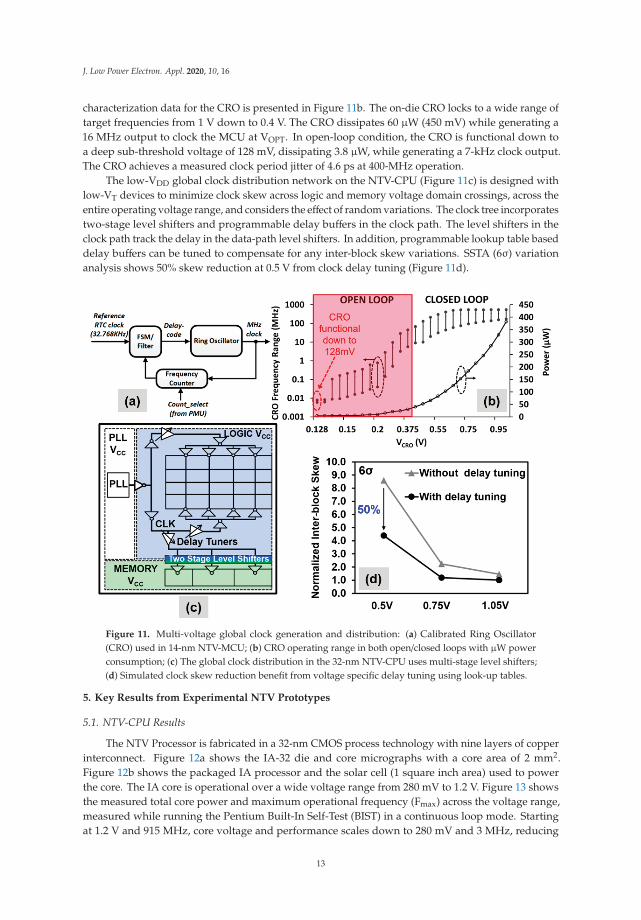
NTV Clocking Architecture
A calibrated ring oscillator (CRO) serves as a low-power on-chip high-frequency (MHz) clocksource for the 14-nm NTV-MCU. The CRO is a frequency-locked loop (Figure 11a) that uses an RTC asa reference to generate a MHz clock output. Internally, the CRO tracks the frequency of oscillation froma ring oscillator and generates a delay code that adjusts the oscillation frequency to closely match thetarget frequency based on the reference clock. The CRO can operate in (1) closed-loop mode, where itaccurately tracks the target frequency, as well as in (2) open loop mode at ultralow voltages, producingclock with tens of KHz frequency, enough for always-on (AON) sensing operation on the MCU. Silicon
12
J. Low Power Electron. Appl. 2020, 10, 16
characterization data for the CRO is presented in Figure 11b. The on-die CRO locks to a wide range oftarget frequencies from 1 V down to 0.4 V. The CRO dissipates 60 μW (450 mV) while generating a16 MHz output to clock the MCU at VOPT. In open-loop condition, the CRO is functional down toa deep sub-threshold voltage of 128 mV, dissipating 3.8 μW, while generating a 7-kHz clock output.The CRO achieves a measured clock period jitter of 4.6 ps at 400-MHz operation.
The low-VDD global clock distribution network on the NTV-CPU (Figure 11c) is designed withlow-VT devices to minimize clock skew across logic and memory voltage domain crossings, across theentire operating voltage range, and considers the effect of random variations. The clock tree incorporatestwo-stage level shifters and programmable delay buffers in the clock path. The level shifters in theclock path track the delay in the data-path level shifters. In addition, programmable lookup table baseddelay buffers can be tuned to compensate for any inter-block skew variations. SSTA (6σ) variationanalysis shows 50% skew reduction at 0.5 V from clock delay tuning (Figure 11d).
Figure 11. Multi-voltage global clock generation and distribution: (a) Calibrated Ring Oscillator(CRO) used in 14-nm NTV-MCU; (b) CRO operating range in both open/closed loops with μW powerconsumption; (c) The global clock distribution in the 32-nm NTV-CPU uses multi-stage level shifters;(d) Simulated clock skew reduction benefit from voltage specific delay tuning using look-up tables.
5. Key Results from Experimental NTV Prototypes
5.1. NTV-CPU Results
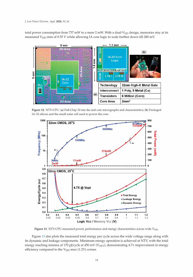
The NTV Processor is fabricated in a 32-nm CMOS process technology with nine layers of copperinterconnect. Figure 12a shows the IA-32 die and core micrographs with a core area of 2 mm2.Figure 12b shows the packaged IA processor and the solar cell (1 square inch area) used to powerthe core. The IA core is operational over a wide voltage range from 280 mV to 1.2 V. Figure 13 showsthe measured total core power and maximum operational frequency (Fmax) across the voltage range,measured while running the Pentium Built-In Self-Test (BIST) in a continuous loop mode. Startingat 1.2 V and 915 MHz, core voltage and performance scales down to 280 mV and 3 MHz, reducing
13
J. Low Power Electron. Appl. 2020, 10, 16
total power consumption from 737 mW to a mere 2 mW. With a dual-VDD design, memories stay at itsmeasured VDD-min of 0.55 V while allowing IA core logic to scale further down till 280 mV.
Figure 12. NTV-CPU: (a) Full-Chip 32-nm die and core micrographs and characteristics; (b) PackagedIA-32 silicon and the small solar cell used to power the core.
Figure 13. NTV-CPU measured power, performance and energy characteristics across wide VDD.
Figure 13 also plots the measured total energy per cycle across the wide voltage range along withits dynamic and leakage components. Minimum energy operation is achieved at NTV, with the totalenergy reaching minima of 170 pJ/cycle at 450 mV (VOPT), demonstrating 4.7× improvement in energyefficiency compared to the VDD-max (1.2V) corner.
14
J. Low Power Electron. Appl. 2020, 10, 16
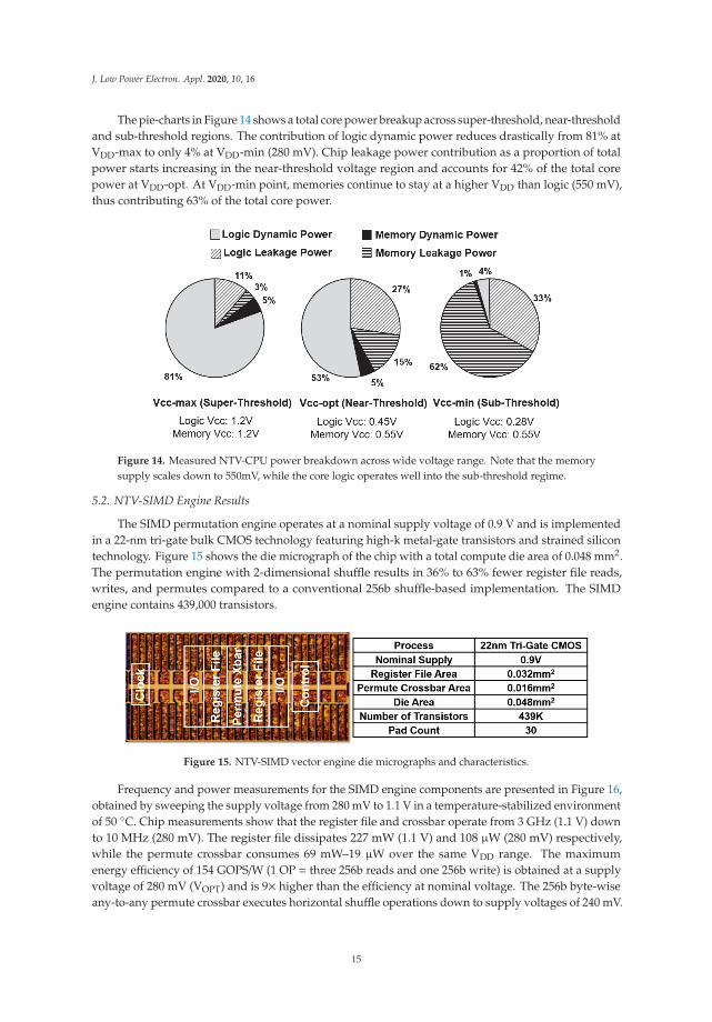
The pie-charts in Figure 14 shows a total core power breakup across super-threshold, near-thresholdand sub-threshold regions. The contribution of logic dynamic power reduces drastically from 81% atVDD-max to only 4% at VDD-min (280 mV). Chip leakage power contribution as a proportion of totalpower starts increasing in the near-threshold voltage region and accounts for 42% of the total corepower at VDD-opt. At VDD-min point, memories continue to stay at a higher VDD than logic (550 mV),thus contributing 63% of the total core power.
Figure 14. Measured NTV-CPU power breakdown across wide voltage range. Note that the memorysupply scales down to 550mV, while the core logic operates well into the sub-threshold regime.
5.2. NTV-SIMD Engine Results
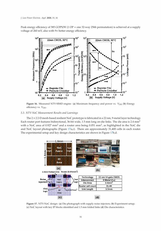
The SIMD permutation engine operates at a nominal supply voltage of 0.9 V and is implementedin a 22-nm tri-gate bulk CMOS technology featuring high-k metal-gate transistors and strained silicontechnology. Figure 15 shows the die micrograph of the chip with a total compute die area of 0.048 mm2.The permutation engine with 2-dimensional shuffle results in 36% to 63% fewer register file reads,writes, and permutes compared to a conventional 256b shuffle-based implementation. The SIMDengine contains 439,000 transistors.
Figure 15. NTV-SIMD vector engine die micrographs and characteristics.
Frequency and power measurements for the SIMD engine components are presented in Figure 16,obtained by sweeping the supply voltage from 280 mV to 1.1 V in a temperature-stabilized environmentof 50 ◦C. Chip measurements show that the register file and crossbar operate from 3 GHz (1.1 V) downto 10 MHz (280 mV). The register file dissipates 227 mW (1.1 V) and 108 μW (280 mV) respectively,while the permute crossbar consumes 69 mW–19 μW over the same VDD range. The maximumenergy efficiency of 154 GOPS/W (1 OP = three 256b reads and one 256b write) is obtained at a supplyvoltage of 280 mV (VOPT) and is 9× higher than the efficiency at nominal voltage. The 256b byte-wiseany-to-any permute crossbar executes horizontal shuffle operations down to supply voltages of 240 mV.
15
J. Low Power Electron. Appl. 2020, 10, 16
Peak energy efficiency of 585 GOPS/W (1 OP = one 32-way 256b permutation) is achieved at a supplyvoltage of 260 mV, also with 9× better energy efficiency.
Figure 16. Measured NTV-SIMD engine: (a) Maximum frequency and power vs. VDD (b) Energyefficiency vs. VDD.
5.3. NTV-NoC Measurement Results and Learnings
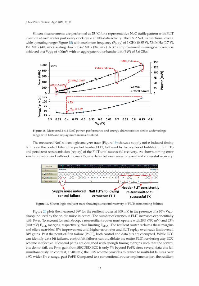
The 2× 2 2-D mesh-based resilient NoC prototype is fabricated in a 22 nm, 9-metal layer technology.Each router port features bidirectional, 36-bit wide, 1.5 mm long on-die links. The die area is 2.4 mm2
with a NoC area of 0.927 mm2 and a router area being 0.051 mm2, as highlighted in the NoC dieand NoC layout photographs (Figure 17a,c). There are approximately 31,400 cells in each router.The experimental setup and key design characteristics are shown in Figure 17b,d.
Figure 17. NTV-NoC design: (a) Die photograph with supply noise injectors; (b) Experiment setup;(c) NoC layout with key IP blocks identified and 1.5 mm folded links (d) Die characteristics.
16
J. Low Power Electron. Appl. 2020, 10, 16
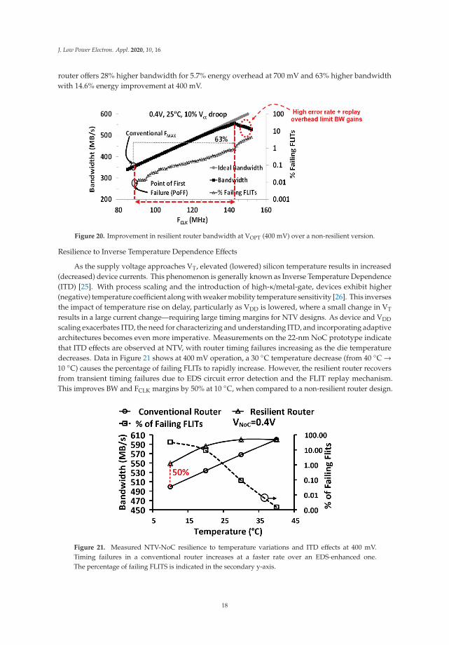
Silicon measurements are performed at 25 ◦C for a representative NoC traffic pattern with FLITinjection at each router port every clock cycle at 10% data activity. The 2 × 2 NoC is functional over awide operating range (Figure 18) with maximum frequency (FMAX) of 1 GHz (0.85 V), 734 MHz (0.7 V),151 MHz (400 mV), scaling down to 67 MHz (340 mV). A 3.3X improvement in energy-efficiency isachieved at a VOPT of 400mV with an aggregate router bandwidth (BW) of 3.6 GB/s.
Figure 18. Measured 2 × 2 NoC power, performance and energy characteristics across wide voltagerange with EDS and replay mechanisms disabled.
The measured NoC silicon logic analyzer trace (Figure 19) shows a supply noise-induced timingfailure on the control bits of the packet header FLIT, followed by two cycles of bubble (null) FLITSand persistent retransmission (replay) of the FLIT until successful recovery. As shown, timing errorsynchronization and roll-back incurs a 2-cycle delay between an error event and successful recovery.
Figure 19. Silicon logic analyzer trace showing successful recovery of FLITs from timing failures.
Figure 20 plots the measured BW for the resilient router at 400 mV, in the presence of a 10% VNoC
droop induced by the on-die noise injectors. The number of erroneous FLIT increases exponentiallywith FCLK. To account for such droop, a non-resilient router must operate with 28% (700 mV) and 63%(400 mV) FCLK margins, respectively, thus limiting FMAX. The resilient router reclaims these marginsand offers near-ideal BW improvement until higher error rates and FLIT replay overheads limit overallBW gains. Past the point-of-first failure (PoFF), both control and data bits are corrupted. While ECCcan identify data bit failures, control bit failures can invalidate the entire FLIT, rendering any ECCscheme ineffective. If control paths are designed with enough timing margins such that the controlbits do not fail, the FCLK gain from SECDED ECC is only 7% beyond PoFF, since several data bits failsimultaneously. In contrast, at 400 mV, the EDS scheme provides tolerance to multi-bit failures overa 9X wider FCLK range, past PoFF. Compared to a conventional router implementation, the resilient
17
J. Low Power Electron. Appl. 2020, 10, 16
router offers 28% higher bandwidth for 5.7% energy overhead at 700 mV and 63% higher bandwidthwith 14.6% energy improvement at 400 mV.
Figure 20. Improvement in resilient router bandwidth at VOPT (400 mV) over a non-resilient version.
Resilience to Inverse Temperature Dependence Effects
As the supply voltage approaches VT, elevated (lowered) silicon temperature results in increased(decreased) device currents. This phenomenon is generally known as Inverse Temperature Dependence(ITD) [25]. With process scaling and the introduction of high-κ/metal-gate, devices exhibit higher(negative) temperature coefficient along with weaker mobility temperature sensitivity [26]. This inversesthe impact of temperature rise on delay, particularly as VDD is lowered, where a small change in VT
results in a large current change—requiring large timing margins for NTV designs. As device and VDD
scaling exacerbates ITD, the need for characterizing and understanding ITD, and incorporating adaptivearchitectures becomes even more imperative. Measurements on the 22-nm NoC prototype indicatethat ITD effects are observed at NTV, with router timing failures increasing as the die temperaturedecreases. Data in Figure 21 shows at 400 mV operation, a 30 ◦C temperature decrease (from 40 ◦C→10 ◦C) causes the percentage of failing FLITs to rapidly increase. However, the resilient router recoversfrom transient timing failures due to EDS circuit error detection and the FLIT replay mechanism.This improves BW and FCLK margins by 50% at 10 ◦C, when compared to a non-resilient router design.
Figure 21. Measured NTV-NoC resilience to temperature variations and ITD effects at 400 mV.Timing failures in a conventional router increases at a faster rate over an EDS-enhanced one.The percentage of failing FLITS is indicated in the secondary y-axis.
18
J. Low Power Electron. Appl. 2020, 10, 16
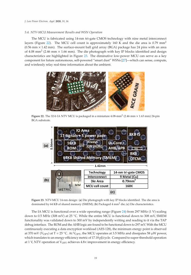
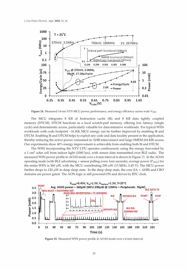
5.4. NTV-MCU Measurement Results and WSN Operation
The MCU is fabricated using 14-nm tri-gate CMOS technology with nine metal interconnectlayers (Figure 22). The MCU cell count is approximately 160 K and the die area is 0.79 mm2
(0.56 mm × 1.42 mm). The surface-mount ball grid array (BGA) package has 24 pins with an areaof 4.08 mm2 (2.46 mm × 1.66 mm). The die photograph with key IP blocks identified and designcharacteristics are highlighted in Figure 23. The diminutive low-power MCU can serve as a keycomponent for future autonomous, self-powered “smart dust” WSNs [27]—which can sense, compute,and wirelessly relay real-time information about the ambient.
Figure 22. The 32-b IA NTV MCU is packaged in a miniature 4.08-mm2 (2.46 mm × 1.63 mm) 24-pinBGA substrate.
Figure 23. NTV-MCU 14-nm design: (a) Die photograph with key IP blocks identified. The die area isdominated by 64 KB of shared memory (SMEM); (b) Packaged 4 mm2 die; (c) Die characteristics.
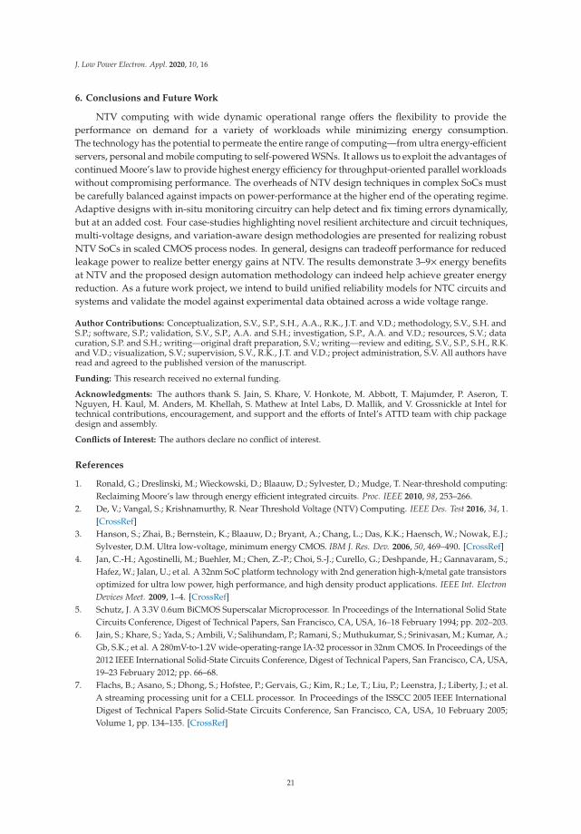
The IA MCU is functional over a wide operating range (Figure 24) from 297 MHz (1 V) scalingdown to 0.5 MHz (308 mV) at 25 ◦C. While the entire MCU is functional down to 308 mV, SMEMfunctionality was validated down to 300 mV by independently writing and reading to it via the TAPdebug interface. The ROM and the AHB logic are found to be functional down to 297 mV. With the MCUcontinuously executing a data encryption workload (AES-128), the minimum energy point is observedat 370 mV (VOPT) at T = 25 ◦C. At VOPT, the MCU operates at 3.5 MHz and dissipates 58 μW power,which translates to an energy-efficiency metric of 17.18 pJ/cycle. Compared to super-threshold operationat 1 V, NTV operation at VOPT achieves 4.8× improvement in energy efficiency.
19
J. Low Power Electron. Appl. 2020, 10, 16
Figure 24. Measured 14-nm NTV-MCU power, performance, and energy efficiency across wide VDD.
The MCU integrates 8 KB of Instruction cache (I$) and 8 KB data tightly coupledmemory (DTCM). DTCM functions as a local scratch-pad memory, offering low latency (singlecycle) and deterministic access, particularly valuable for data-intensive workloads. For typical WSNworkloads with code footprint ~16 KB, MCU energy can be further improved by enabling I$ andDTCM. Enabling I$ and DTCM helps to exploit any code and data locality present in the application,thereby reducing the active power consumed in AHB interconnect and large SMEM (64 KB) access.Our experiments show 40% energy improvement is achievable from enabling both I$ and DTCM.
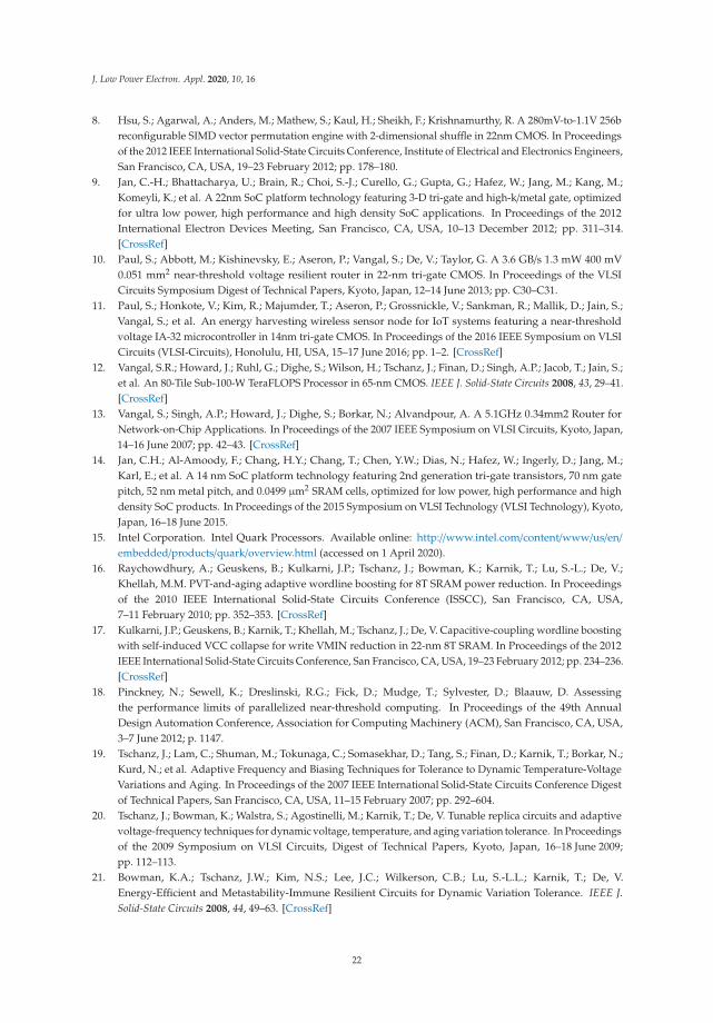
The WSN incorporating the NTV CPU operates continuously using the energy harvested bya 1 cm2 solar cell from indoor light (1000 lux), with sensor data transmitted over BLE radio. Themeasured WSN power profile in AOAS mode over a 4-min interval is shown in Figure 25. In the AOASoperating mode (with BLE advertising + sensor polling every four seconds), average power (PAVG) forthe entire WSN is 360 μW, with the MCU contributing 290 μW (13 MHz, 0.45 V). The MCU powerfurther drops to 120 μW in deep sleep state. In the deep sleep state, the core (IA + AHB) and CROdomains are power gated. The AON logic is still powered-ON and driven by RTC clock.
Figure 25. Measured WSN power profile in AOAS mode over a 4-min interval.
20
J. Low Power Electron. Appl. 2020, 10, 16
6. Conclusions and Future Work
NTV computing with wide dynamic operational range offers the flexibility to provide theperformance on demand for a variety of workloads while minimizing energy consumption.The technology has the potential to permeate the entire range of computing—from ultra energy-efficientservers, personal and mobile computing to self-powered WSNs. It allows us to exploit the advantages ofcontinued Moore’s law to provide highest energy efficiency for throughput-oriented parallel workloadswithout compromising performance. The overheads of NTV design techniques in complex SoCs mustbe carefully balanced against impacts on power-performance at the higher end of the operating regime.Adaptive designs with in-situ monitoring circuitry can help detect and fix timing errors dynamically,but at an added cost. Four case-studies highlighting novel resilient architecture and circuit techniques,multi-voltage designs, and variation-aware design methodologies are presented for realizing robustNTV SoCs in scaled CMOS process nodes. In general, designs can tradeoff performance for reducedleakage power to realize better energy gains at NTV. The results demonstrate 3–9× energy benefitsat NTV and the proposed design automation methodology can indeed help achieve greater energyreduction. As a future work project, we intend to build unified reliability models for NTC circuits andsystems and validate the model against experimental data obtained across a wide voltage range.
Author Contributions: Conceptualization, S.V., S.P., S.H., A.A., R.K., J.T. and V.D.; methodology, S.V., S.H. andS.P.; software, S.P.; validation, S.V., S.P., A.A. and S.H.; investigation, S.P., A.A. and V.D.; resources, S.V.; datacuration, S.P. and S.H.; writing—original draft preparation, S.V.; writing—review and editing, S.V., S.P., S.H., R.K.and V.D.; visualization, S.V.; supervision, S.V., R.K., J.T. and V.D.; project administration, S.V. All authors haveread and agreed to the published version of the manuscript.
Funding: This research received no external funding.
Acknowledgments: The authors thank S. Jain, S. Khare, V. Honkote, M. Abbott, T. Majumder, P. Aseron, T.Nguyen, H. Kaul, M. Anders, M. Khellah, S. Mathew at Intel Labs, D. Mallik, and V. Grossnickle at Intel fortechnical contributions, encouragement, and support and the efforts of Intel’s ATTD team with chip packagedesign and assembly.
Conflicts of Interest: The authors declare no conflict of interest.
References
1. Ronald, G.; Dreslinski, M.; Wieckowski, D.; Blaauw, D.; Sylvester, D.; Mudge, T. Near-threshold computing:Reclaiming Moore’s law through energy efficient integrated circuits. Proc. IEEE 2010, 98, 253–266.
2. De, V.; Vangal, S.; Krishnamurthy, R. Near Threshold Voltage (NTV) Computing. IEEE Des. Test 2016, 34, 1.[CrossRef]
3. Hanson, S.; Zhai, B.; Bernstein, K.; Blaauw, D.; Bryant, A.; Chang, L.; Das, K.K.; Haensch, W.; Nowak, E.J.;Sylvester, D.M. Ultra low-voltage, minimum energy CMOS. IBM J. Res. Dev. 2006, 50, 469–490. [CrossRef]
4. Jan, C.-H.; Agostinelli, M.; Buehler, M.; Chen, Z.-P.; Choi, S.-J.; Curello, G.; Deshpande, H.; Gannavaram, S.;Hafez, W.; Jalan, U.; et al. A 32nm SoC platform technology with 2nd generation high-k/metal gate transistorsoptimized for ultra low power, high performance, and high density product applications. IEEE Int. ElectronDevices Meet. 2009, 1–4. [CrossRef]
5. Schutz, J. A 3.3V 0.6um BiCMOS Superscalar Microprocessor. In Proceedings of the International Solid StateCircuits Conference, Digest of Technical Papers, San Francisco, CA, USA, 16–18 February 1994; pp. 202–203.
6. Jain, S.; Khare, S.; Yada, S.; Ambili, V.; Salihundam, P.; Ramani, S.; Muthukumar, S.; Srinivasan, M.; Kumar, A.;Gb, S.K.; et al. A 280mV-to-1.2V wide-operating-range IA-32 processor in 32nm CMOS. In Proceedings of the2012 IEEE International Solid-State Circuits Conference, Digest of Technical Papers, San Francisco, CA, USA,19–23 February 2012; pp. 66–68.
7. Flachs, B.; Asano, S.; Dhong, S.; Hofstee, P.; Gervais, G.; Kim, R.; Le, T.; Liu, P.; Leenstra, J.; Liberty, J.; et al.A streaming processing unit for a CELL processor. In Proceedings of the ISSCC 2005 IEEE InternationalDigest of Technical Papers Solid-State Circuits Conference, San Francisco, CA, USA, 10 February 2005;Volume 1, pp. 134–135. [CrossRef]
21
J. Low Power Electron. Appl. 2020, 10, 16
8. Hsu, S.; Agarwal, A.; Anders, M.; Mathew, S.; Kaul, H.; Sheikh, F.; Krishnamurthy, R. A 280mV-to-1.1V 256breconfigurable SIMD vector permutation engine with 2-dimensional shuffle in 22nm CMOS. In Proceedingsof the 2012 IEEE International Solid-State Circuits Conference, Institute of Electrical and Electronics Engineers,San Francisco, CA, USA, 19–23 February 2012; pp. 178–180.
9. Jan, C.-H.; Bhattacharya, U.; Brain, R.; Choi, S.-J.; Curello, G.; Gupta, G.; Hafez, W.; Jang, M.; Kang, M.;Komeyli, K.; et al. A 22nm SoC platform technology featuring 3-D tri-gate and high-k/metal gate, optimizedfor ultra low power, high performance and high density SoC applications. In Proceedings of the 2012International Electron Devices Meeting, San Francisco, CA, USA, 10–13 December 2012; pp. 311–314.[CrossRef]
10. Paul, S.; Abbott, M.; Kishinevsky, E.; Aseron, P.; Vangal, S.; De, V.; Taylor, G. A 3.6 GB/s 1.3 mW 400 mV0.051 mm2 near-threshold voltage resilient router in 22-nm tri-gate CMOS. In Proceedings of the VLSICircuits Symposium Digest of Technical Papers, Kyoto, Japan, 12–14 June 2013; pp. C30–C31.
11. Paul, S.; Honkote, V.; Kim, R.; Majumder, T.; Aseron, P.; Grossnickle, V.; Sankman, R.; Mallik, D.; Jain, S.;Vangal, S.; et al. An energy harvesting wireless sensor node for IoT systems featuring a near-thresholdvoltage IA-32 microcontroller in 14nm tri-gate CMOS. In Proceedings of the 2016 IEEE Symposium on VLSICircuits (VLSI-Circuits), Honolulu, HI, USA, 15–17 June 2016; pp. 1–2. [CrossRef]
12. Vangal, S.R.; Howard, J.; Ruhl, G.; Dighe, S.; Wilson, H.; Tschanz, J.; Finan, D.; Singh, A.P.; Jacob, T.; Jain, S.;et al. An 80-Tile Sub-100-W TeraFLOPS Processor in 65-nm CMOS. IEEE J. Solid-State Circuits 2008, 43, 29–41.[CrossRef]
13. Vangal, S.; Singh, A.P.; Howard, J.; Dighe, S.; Borkar, N.; Alvandpour, A. A 5.1GHz 0.34mm2 Router forNetwork-on-Chip Applications. In Proceedings of the 2007 IEEE Symposium on VLSI Circuits, Kyoto, Japan,14–16 June 2007; pp. 42–43. [CrossRef]
14. Jan, C.H.; Al-Amoody, F.; Chang, H.Y.; Chang, T.; Chen, Y.W.; Dias, N.; Hafez, W.; Ingerly, D.; Jang, M.;Karl, E.; et al. A 14 nm SoC platform technology featuring 2nd generation tri-gate transistors, 70 nm gatepitch, 52 nm metal pitch, and 0.0499 μm2 SRAM cells, optimized for low power, high performance and highdensity SoC products. In Proceedings of the 2015 Symposium on VLSI Technology (VLSI Technology), Kyoto,Japan, 16–18 June 2015.
15. Intel Corporation. Intel Quark Processors. Available online: http://www.intel.com/content/www/us/en/embedded/products/quark/overview.html (accessed on 1 April 2020).
16. Raychowdhury, A.; Geuskens, B.; Kulkarni, J.P.; Tschanz, J.; Bowman, K.; Karnik, T.; Lu, S.-L.; De, V.;Khellah, M.M. PVT-and-aging adaptive wordline boosting for 8T SRAM power reduction. In Proceedingsof the 2010 IEEE International Solid-State Circuits Conference (ISSCC), San Francisco, CA, USA,7–11 February 2010; pp. 352–353. [CrossRef]
17. Kulkarni, J.P.; Geuskens, B.; Karnik, T.; Khellah, M.; Tschanz, J.; De, V. Capacitive-coupling wordline boostingwith self-induced VCC collapse for write VMIN reduction in 22-nm 8T SRAM. In Proceedings of the 2012IEEE International Solid-State Circuits Conference, San Francisco, CA, USA, 19–23 February 2012; pp. 234–236.[CrossRef]
18. Pinckney, N.; Sewell, K.; Dreslinski, R.G.; Fick, D.; Mudge, T.; Sylvester, D.; Blaauw, D. Assessingthe performance limits of parallelized near-threshold computing. In Proceedings of the 49th AnnualDesign Automation Conference, Association for Computing Machinery (ACM), San Francisco, CA, USA,3–7 June 2012; p. 1147.
19. Tschanz, J.; Lam, C.; Shuman, M.; Tokunaga, C.; Somasekhar, D.; Tang, S.; Finan, D.; Karnik, T.; Borkar, N.;Kurd, N.; et al. Adaptive Frequency and Biasing Techniques for Tolerance to Dynamic Temperature-VoltageVariations and Aging. In Proceedings of the 2007 IEEE International Solid-State Circuits Conference Digestof Technical Papers, San Francisco, CA, USA, 11–15 February 2007; pp. 292–604.
20. Tschanz, J.; Bowman, K.; Walstra, S.; Agostinelli, M.; Karnik, T.; De, V. Tunable replica circuits and adaptivevoltage-frequency techniques for dynamic voltage, temperature, and aging variation tolerance. In Proceedingsof the 2009 Symposium on VLSI Circuits, Digest of Technical Papers, Kyoto, Japan, 16–18 June 2009;pp. 112–113.
21. Bowman, K.A.; Tschanz, J.W.; Kim, N.S.; Lee, J.C.; Wilkerson, C.B.; Lu, S.-L.L.; Karnik, T.; De, V.Energy-Efficient and Metastability-Immune Resilient Circuits for Dynamic Variation Tolerance. IEEE J.Solid-State Circuits 2008, 44, 49–63. [CrossRef]
22
J. Low Power Electron. Appl. 2020, 10, 16
22. Rossi, D.; Metra, C.; Nieuwland, A.K.; Katoch, A. New ECC for crosstalk effect minimization. IEEE Des.Test Comput. 2005, 22, 340–348. [CrossRef]
23. Amin, C.S.; Menezes, N.; Killpack, K.; Dartu, F.; Choudhury, U.; Hakim, N.; Ismail, Y.I. Statistical statictiming analysis. In Proceedings of the 42nd Design Automation Conference, Association for ComputingMachinery (ACM), Anaheim, CA, USA, 13–17 June 2005; p. 652.
24. Singhee, A.; Singhal, S.; Rutenbar, R.A. Practical, fast Monte Carlo statistical static timing analysis: Whyand how. In Proceedings of the 2008 IEEE/ACM International Conference on Computer-Aided Design, SanJose, CA, USA, 10–13 November 2008; pp. 190–195.
25. Cho, M.; Khellah, M.; Chae, K.; Ahmed, K.; Tschanz, J.; Mukhopadhyay, S. Characterization of InverseTemperature Dependence in logic circuits. In Proceedings of the IEEE 2012 Custom Integrated CircuitsConference, San Jose, CA, USA, 9–12 September 2012; pp. 1–4.
26. Han, S.; Guo, D.; Wang, X.; Mocuta, A.C.; Henson, W.K.; Rim, K. Reverse Temperature Dependence of CircuitPerformance in High-k/Metal-Gate Technology. IEEE Electron Device Lett. 2009, 30, 1344–1346.
27. Warneke, B.; Last, M.; Liebowitz, B.; Pister, K. Smart Dust: Communicating with a cubic-millimeter computer.Computer 2001, 34, 44–51. [CrossRef]
© 2020 by the authors. Licensee MDPI, Basel, Switzerland. This article is an open accessarticle distributed under the terms and conditions of the Creative Commons Attribution(CC BY) license (http://creativecommons.org/licenses/by/4.0/).
23

Journal of
Low Power Electronicsand Applications
Article
Cross-Layer Reliability, Energy Efficiency,and Performance Optimization of Near-ThresholdData Paths
Mehdi Tahoori * and Mohammad Saber Golanbari
Dependable Nano Computing, Karlsruhe Institute of Technology, 76131 Karlsruhe, Germany; [email protected]* Correspondence: [email protected]; Tel.: +49-721-608-47778
Received: 6 September 2020; Accepted: 18 November 2020; Published: 3 December 2020
Abstract: Modern electronic devices are an indispensable part of our everyday life. A major enablerfor such integration is the exponential increase of the computation capabilities as well as the drasticimprovement in the energy efficiency over the last 50 years, commonly known as Moore’s law. In thisregard, the demand for energy-efficient digital circuits, especially for application domains such as theInternet of Things (IoT), has faced an enormous growth. Since the power consumption of a circuithighly depends on the supply voltage, aggressive supply voltage scaling to the near-threshold voltageregion, also known as Near-Threshold Computing (NTC), is an effective way of increasing the energyefficiency of a circuit by an order of magnitude. However, NTC comes with specific challenges withrespect to performance and reliability, which mandates new sets of design techniques to fully harness itspotential. While techniques merely focused at one abstraction level, in particular circuit-level design,can have limited benefits, cross-layer approaches result in far better optimizations. This paper presentsinstruction multi-cycling and functional unit partitioning methods to improve energy efficiency andresiliency of functional units. The proposed methods significantly improve the circuit timing, and at thesame time considerably limit leakage energy, by employing a combination of cross-layer techniques basedon circuit redesign and code replacement techniques. Simulation results show that the proposed methodsimprove performance and energy efficiency of an Arithmetic Logic Unit by 19% and 43%, respectively.Furthermore, the improved performance of the optimized circuits can be traded to improving thereliability.
Keywords: reliability; Near-Threshold Computing; functional unit; energy efficiency; performanceoptimization; cross-layer optimization
1. Introduction
Since the advent of electronic digital computing, relentless technology scaling has enabled anexponential improvement in computation capability while decreasing the cost and power consumption.Gordon Moore predicted in 1965 that the number of transistors in integrated circuits would double everyyear to address the ever-increasing demand for higher computation power [1] (this prediction was adjustedafterward to reflect the real progress [2,3]). Such continuous growth in computation capability over morethan five decades affected almost all aspects of human life, including but not limited to industry, business,health-care, government, and society, which effectively started the Information Age, and made digitalcomputing circuits an inseparable part of our everyday life.
J. Low Power Electron. Appl. 2020, 10, 42; doi:10.3390/jlpea10040042 www.mdpi.com/journal/jlpea
25
J. Low Power Electron. Appl. 2020, 10, 42
Moore’s law has faced several technological challenges and has been slowed down in the pastdecade [2,4,5]; however, still more transistors can be integrated on every new technology generation downto a 3 nm node [6,7].
To avoid exponential growth in the power density, various parameters including supply voltage ofdigital circuits have been scaled according to Dennard’s scaling law [8]. However, the supply voltagedid not scale at the same pace for about one decade (since 2005–2006) due to technological challengesassociated with nanometer-scale devices [9]. Since then, various architectural and design directions havebeen actively explored including many-core computation, parallel processing, and 3D integration toprovide more computation power [5–7]. However, the main challenges caused by the end of Dennard’sscaling are energy efficiency and power density, which cannot be addressed by such approaches [10–12].Without proper addressing of the increasing power density due to technology scaling, it is not possible toutilize all the components of a chip at the same time due to overheating, a problem commonly knownas Dark Silicon [11,13], which diminishes the benefits of scaling. Therefore, reducing the power densitythrough improving the energy efficiency is pivotal for future digital circuits.
In fact, energy-efficient computing has already become a primary requirement in various applicationdomains. At one end of the spectrum, the growing IoT applications, with an expected 20 billion connecteddevices by 2020 [14–16], are continually looking for more energy efficiency. These IoT devices are expectedto operate on limited energy sources such as batteries or energy harvesting sources. High-performanceservers and data centers, at the other end, are responsible for a significant amount of consumed electricityworldwide (about 1.4% of the consumed electricity worldwide in 2011, and growing in much faster speedcompared to other electricity consumers) [17]. A large portion of the cost of data centers is directly orindirectly due to the energy consumption of digital circuits [17]; hence, it is necessary to improve theenergy efficiency of high-performance computing as well.
Power consumption of digital circuits has two components: dynamic power consumption, due tocircuit activity and computation, and leakage power consumption, due to slight leakage current oftransistors. Reducing the power density can be achieved through various approaches such as optimizingdesign techniques, employing power management strategies, improving the technology, and scalingsupply voltage [18]. Each of these approaches aims at reducing dynamic power, leakage power, orboth. In this regard, optimizing Instruction Set Architecture (ISA), scheduling methods, pipeline design,and synthesis methodologies have already enabled vast improvements in the energy efficiency [19].
Techniques such as clock-gating and power-gating are widely used in existing digital circuits to cutdown dynamic and leakage power of the idle components [20]. Dynamic Voltage and Frequency Scaling(DVFS) promotes supply voltage and speed adaptation depending on the workload to reduce powerconsumption under low workload [21,22].
Aggressive supply voltage reduction down to the sub-threshold region is known as an importantinstrument, which reduces power consumption by several orders of magnitude and improves energyefficiency [12,18,23–25]. Intel has demonstrated ultra-low power characteristics using such aggressivevoltage scaling by its experimental IA32 processor, which can run Windows and Linux on a small solarpanel [26]. In addition to extensive power reduction, voltage scaling degrades circuit speed significantly.Many applications have performance constraints that prevent them from operating in the sub-thresholdregion.
By operating digital circuits at supply voltages close to the threshold voltage of the transistors, which isknown as NTC, it is still possible to gain very high energy efficiency and achieve enough performance formany applications in the IoT domain [27,28]. Additionally, many-core computation based on NTC is anattractive approach to improve energy efficiency while satisfying the computational demands for highlyparallel workloads of data centers [10,29–31]. Therefore, NTC is considered an attractive paradigm forimproving the energy efficiency in modern technology nodes [32], if the associated reliability challenges
26
J. Low Power Electron. Appl. 2020, 10, 42
are addressed. These reliability challenges are typically caused by enormous sensitivity of NTC circuits tovariability sources and complicate NTC circuit design and operation.
Along with the enormous energy benefits, NTC comes with a variety of design challenges. The mostobvious one is the performance reduction of 10× compared to the super-threshold domain, which maylimit the applicability of NTC [27]. In addition, the escalated sensitivity to variability (such as process andvoltage variation) at reduced supply voltages forces designers to add very conservative and expensivetiming margins to achieve acceptable yield and reliability [33].
Moreover, in the near-threshold region leakage energy becomes comparable to dynamic energy,thus approaches to minimize leakage are of uttermost importance for NTC designs. Hence, althoughconventional designs can technically operate in the NTC domain, due to these challenges, new designparadigms have to be developed for NTC to harness its full potential.
Data paths are core components of any processing element such as processor cores and accelerators.A data path consists of various functional units, such as Arithmetic Logic Unit (ALU) and Floating PointUnit (FPU), the timing and power consumption characteristics of which significantly impact the overallperformance of the processor. Therefore, optimizing the reliability, energy efficiency, and performance ofdata paths is of decisive importance.
This paper presents two cross-layer functional unit optimization opportunities based on (1) instructionmulti-cycling and (2) functional unit partitioning, which improve energy-efficiency, reliability,and performance. We evaluate our methodology by using an ALU implemented for Alpha ISA. Our resultsshow that the proposed approach can effectively improve energy efficiency and reliability. For example,instruction multi-cycling effectively removes the extra timing slacks and improves the energy efficiency ofa circuit by up to 34%. Furthermore, the functional unit partitioning approach can improve the energyefficiency of an ALU by 43.4% while having positive impacts on the reliability and performance as well.
The rest of this paper is organized as follows. Section 2 provides the background on nearthreshold computing. Section 3 reviews the state-of-the-art and their shortcomings. The optimizationapproaches based on instruction multi-cycling and functional unit partitioning are presented in Section 4,while Section 5 discusses the optimization results. Finally, Section 6 concludes the paper.
2. Near-Threshold Computing
Various methodologies at different abstraction-levels have been proposed andemployed [18–22,34–36] to improve the energy efficiency and overcome the power wall challengecaused by the end of Dennard’s scaling [9–12]. Aggressive supply voltage scaling down to thesub-threshold region [12,18,23–25] is also presented as an effective way to reduce the power consumptionby several orders of magnitude; however, the speed of digital circuits at that supply voltage range ispoor. In the following, we present a promising approach towards supply voltage scaling, called NTC,which also retains enough performance for many applications.
Near-Threshold Computing is a paradigm in which the supply voltage is reduced close to thethreshold voltage of transistors to gain large energy efficiency while retaining enough performance formany applications. However, there are various challenges towards NTC mainly in the area of reliabilityand energy efficiency, which can nullify the benefits of NTC if not addressed correctly. This paper focuseson the NTC and its challenges.
From a circuit-level point of view, the total power consumption of a circuit can be calculated as inEquation (1):
Ptotal = Pdyn,sw + Pdyn,sc + Pleak, (1)
where Pdyn,sw, Pdyn,sc, and Pleak are dynamic switching power, dynamic short-circuit power, and leakagepower, respectively.
27
J. Low Power Electron. Appl. 2020, 10, 42
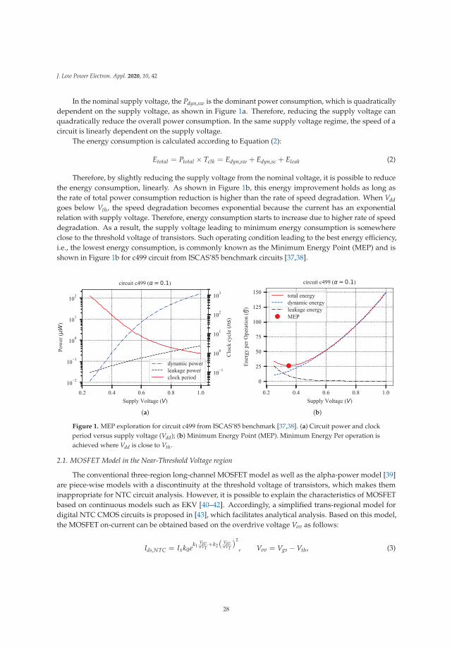
In the nominal supply voltage, the Pdyn,sw is the dominant power consumption, which is quadraticallydependent on the supply voltage, as shown in Figure 1a. Therefore, reducing the supply voltage canquadratically reduce the overall power consumption. In the same supply voltage regime, the speed of acircuit is linearly dependent on the supply voltage.
The energy consumption is calculated according to Equation (2):
Etotal = Ptotal × Tclk = Edyn,sw + Edyn,sc + Eleak (2)
Therefore, by slightly reducing the supply voltage from the nominal voltage, it is possible to reducethe energy consumption, linearly. As shown in Figure 1b, this energy improvement holds as long asthe rate of total power consumption reduction is higher than the rate of speed degradation. When Vddgoes below Vth, the speed degradation becomes exponential because the current has an exponentialrelation with supply voltage. Therefore, energy consumption starts to increase due to higher rate of speeddegradation. As a result, the supply voltage leading to minimum energy consumption is somewhereclose to the threshold voltage of transistors. Such operating condition leading to the best energy efficiency,i.e., the lowest energy consumption, is commonly known as the Minimum Energy Point (MEP) and isshown in Figure 1b for c499 circuit from ISCAS’85 benchmark circuits [37,38].
(a) (b)
Figure 1. MEP exploration for circuit c499 from ISCAS’85 benchmark [37,38]. (a) Circuit power and clockperiod versus supply voltage (Vdd); (b) Minimum Energy Point (MEP). Minimum Energy Per operation isachieved where Vdd is close to Vth.
2.1. MOSFET Model in the Near-Threshold Voltage region
The conventional three-region long-channel MOSFET model as well as the alpha-power model [39]are piece-wise models with a discontinuity at the threshold voltage of transistors, which makes theminappropriate for NTC circuit analysis. However, it is possible to explain the characteristics of MOSFETbased on continuous models such as EKV [40–42]. Accordingly, a simplified trans-regional model fordigital NTC CMOS circuits is proposed in [43], which facilitates analytical analysis. Based on this model,the MOSFET on-current can be obtained based on the overdrive voltage Vov as follows:
Ids,NTC = Ixk0ek1VovnVT
+k2
(VovnVT
)2
, Vov = Vgs − Vth, (3)
28
J. Low Power Electron. Appl. 2020, 10, 42
where Ix depends on process parameters and transistor dimensions (W, L), whereas k0, k1, and k2 areprocess independent fitting parameters [43]. In the above equation, it is assumed that Vds � VT ; therefore,the term depending on Vds is eliminated. However, it is possible to consider the threshold voltagedependency on Vds and body-biasing. Based on this model, the propagation delay of a gate in theNear-Threshold Voltage (NTV) region is obtained as:
tp,NTC =k f CLVdd
Ixk0e−k1
VdtnVT
−k2
( VdtnVT
)2
, Vdt = Vdd − Vth. (4)
Similarly, energy and power consumption of digital circuits can be calculated in the NTV region [43].
Process, Voltage, and Temperature Variation in NTC
The impacts of process, supply voltage, and temperature variations (PVT) are more pronounced inthe NTV region [27,33,44]. Authors of [45] showed that the sensitivity of the drain-source current of atransistor (Ids) to changes in Vth and Vdd increases by about 10× when the supply voltage is reduced fromthe super-threshold region to the sub-threshold region. Equation (4) also demonstrates that propagationdelay in the NTV region is exponentially dependent on supply and threshold voltages. Intel [33] reportedthat while the process and temperature variations cause 18% and 5% performance variation in thesuper-threshold region, their impacts aggravate to 2× performance variation in the NTV region.
The power consumption of NTC circuits is orders of magnitude smaller than the super-thresholdregion. As a result, runtime supply voltage fluctuation caused by power consumption also decreasesby the same scale, which makes it insignificant in NTC circuits, even considering the large sensitivity tofluctuations. Moreover, the temperature of NTC circuits is solely determined by the ambient temperaturesince the power dissipation is very small and has a negligible impact on circuit temperature fluctuation [46].
2.2. NTC Challenges
2.2.1. Reliability
Aggressive supply voltage scaling to the NTV region has benefits and drawbacks in terms of reliability.Reducing the supply voltage to the NTV region greatly reduces internal electric fields and current densitycompared to the super-threshold region, which helps to protect the circuits from some aging phenomenaand their associated reliability problems.
Nevertheless, the exponential sensitivity to PVT in the NTV region severely affects the circuit behaviorand may lead to large performance variation or reliability issues, in terms of functional failure or timingviolations. As presented in [33], ±2× performance variation is observed between different fabricated NTCcores only due to process variation, whereas this variation was limited to ±18% at the nominal voltage.Techniques such as adaptive body biasing [27] and supply voltage scaling [47] are presented to addresssuch performance fluctuation. Similarly, the maximum clock frequency of an NTC circuit may changeby ±2× due to 110 °C temperature fluctuation, while the impact of such temperature fluctuation onperformance is only 5% at the nominal voltage [33] (the measurement is done for a 65 nm typical die). Anunwanted performance fluctuation at gate-level may lead to timing violations. Setup-time violations canbe addressed by increasing the clock period Tclk (i.e., reducing clock speed f ), which inflicts performanceand energy efficiency loss. Various timing error detection and correction methods have also been proposedto address setup-time issues [48–52], which may be costly as the number of timing errors increases rapidlyin the NTV region. However, a hold-time violation cannot be fixed by changing the clock speed andleads to a functional failure. As an example, the number of hold-time violations increases by up to 16×when operating in the NTV region compared to the nominal voltage [53]. In order to fix these timing
29
J. Low Power Electron. Appl. 2020, 10, 42
violations, many buffers have to be inserted into the violating paths to delay the arrival times of such shortpaths. Therefore, the overhead of buffer insertion in the NTV region is significantly larger than that of thesuper-threshold region.
Reduced noise margin due to voltage scaling is a major challenge in storage component designfor NTC. Conventional 6T SRAM memory cells cannot operate correctly in the NTV region withoutredesigning [54], and 8T or 10T SRAMs are preferred due to better noise margin and resiliency tovariations [55–58]. In addition, due to low activity of memory cells, the optimum supply voltage may beconsiderably higher than core logic. Therefore, voltage level converters may be needed to interface memoryand core cells, which brings additional complexity to routing and Power Delivery Network (PDN) design.Similarly, flip-flops have issues due to reduced noise margin and high sensitivity to variations [27,33].Therefore, various flip-flop designs have been studied for low-voltage operation and are optimized forNTC [27,28,33,59–61]. The soft-error rate of storage components is dependent on the critical charge,which decreases by 5× in the NTV region [62]. Therefore, more soft-errors are observed in the NTV regionin both logic and memory components. Various methods have been proposed at different abstractionlevels from device to architecture-level to address the faults caused by soft-errors for NTC [63–70].
2.2.2. Energy Efficiency
The energy efficiency of NTC circuits is highly dependent on design, process variation, and runtimeparameters. Scaling down the supply voltage changes the ratio of dynamic and leakage power consumptionsignificantly, causing a paradigm shift in design and optimization. Figure 2 presents the powerconsumption of an IA32 processor. The contribution of logic dynamic power decreases from 81% inthe super-threshold region to 4% in the sub-threshold region, whereas the contribution of logic leakagepower increases from 11% to 33% [26]. Therefore, leakage power reduction techniques at architecture-level(e.g., by power-gating schemes) down to device-level (e.g., by incorporating advanced technologies such asFinFET) are more rewarding in the NTV region compared to the super-threshold region, in which leakagepower has a smaller contribution.
30
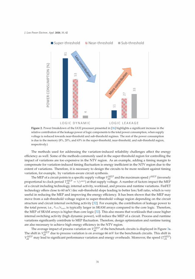
J. Low Power Electron. Appl. 2020, 10, 42
81
11
53
27
4
33
L O G I C D Y N A M I C L O G I C L E A K A G E
POW
ER C
ON
SUM
PTIO
N (%
)Super-threshold Near-threshold Sub-threshold
Figure 2. Power breakdown of the IA32 processor presented in [26] highlights a significant increase in therelative contribution of the leakage power of logic components to the total power consumption, when supplyvoltage is reduced towards near-threshold and sub-threshold regimes. The rest of the power consumptionis due to the memory (8%, 20%, and 63% in the super-threshold, near-threshold, and sub-threshold region,respectively.)
The methods used for addressing the variation-induced reliability challenges affect the energyefficiency as well. Some of the methods commonly used in the super-threshold region for controlling theimpact of variations are too expensive in the NTV region. As an example, adding a timing margin tocompensate for variation-induced timing fluctuation is energy inefficient in the NTV region due to theextent of variations. Therefore, it is necessary to design the circuits to be more resilient against timingvariation, for example, by variation-aware circuit synthesis.
The MEP of a circuit points to a specific supply voltage VMEPdd and the maximum speed f MEP (inversely
proportional to clock period TMEPclk = 1/f MEP) at that supply voltage. A number of factors impact the MEP
of a circuit including technology, internal activity, workload, and process and runtime variations. FinFETtechnology offers close to 60 mV/dec sub-threshold slope leading to better Ion/Ioff ratio, which is veryuseful in reducing the MEP and improving the energy efficiency. It has been shown that the MEP maymove from a sub-threshold voltage region to super-threshold voltage region depending on the circuitstructure and circuit internal switching activity [32]. For example, the contribution of leakage power tothe total power, i.e., Pleak/Ptotal, is typically larger in SRAM arrays compared to the core logic. Therefore,the MEP of SRAM arrays is higher than core logic [32]. This also means that workloads that cause higherinternal switching activity (high dynamic power), will reduce the MEP of a circuit. Process and runtimevariations significantly contribute to MEP fluctuation. Therefore, design optimization and runtime tuningare also necessary to achieve high energy efficiency in the NTV region.
The average impact of process variation on VMEPdd of the benchmark circuits is displayed in Figure 3a.
The shift in VMEPdd due to process variation is on average 66 mV for the benchmark circuits. This shift in
VMEPdd may lead to significant performance variation and energy overheads. Moreover, the speed (TMEP
clk )
31
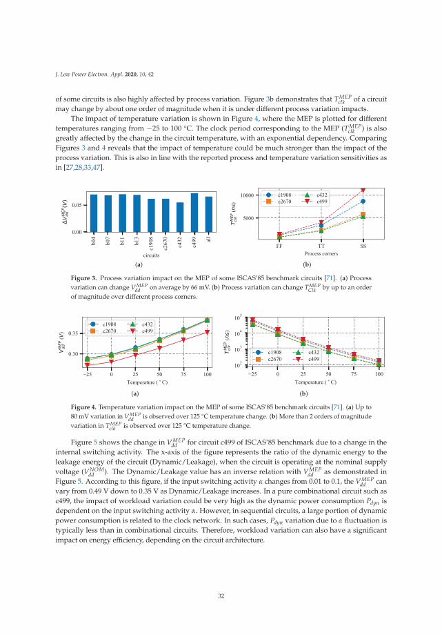
J. Low Power Electron. Appl. 2020, 10, 42
of some circuits is also highly affected by process variation. Figure 3b demonstrates that TMEPclk of a circuit
may change by about one order of magnitude when it is under different process variation impacts.The impact of temperature variation is shown in Figure 4, where the MEP is plotted for different
temperatures ranging from −25 to 100 °C. The clock period corresponding to the MEP (TMEPclk ) is also
greatly affected by the change in the circuit temperature, with an exponential dependency. ComparingFigures 3 and 4 reveals that the impact of temperature could be much stronger than the impact of theprocess variation. This is also in line with the reported process and temperature variation sensitivities asin [27,28,33,47].
b04
b07
b11
b13
c190
8
c267
0
c432
c499 al
l
circuits
0.00
0.05
ΔVMEP
dd(V)
(a)
FF TT SSProcess corners
5000
10000
TMEP
clk
(ns)
c1908c2670
c432c499
(b)
Figure 3. Process variation impact on the MEP of some ISCAS’85 benchmark circuits [71]. (a) Processvariation can change VMEP
dd on average by 66 mV. (b) Process variation can change TMEPClk by up to an order
of magnitude over different process corners.
−25 0 25 50 75 100Temperature ( ∘C)
0.30
0.35
VMEP
dd (V
)
c1908c2670
c432c499
(a)
−25 0 25 50 75 100Temperature ( ∘C)
102
103
104
105
TMEP
clk
(ns)
c1908c2670
c432c499
(b)
Figure 4. Temperature variation impact on the MEP of some ISCAS’85 benchmark circuits [71]. (a) Up to80 mV variation in VMEP
dd is observed over 125 °C temperature change. (b) More than 2 orders of magnitudevariation in TMEP
clk is observed over 125 °C temperature change.
Figure 5 shows the change in VMEPdd for circuit c499 of ISCAS’85 benchmark due to a change in the
internal switching activity. The x-axis of the figure represents the ratio of the dynamic energy to theleakage energy of the circuit (Dynamic/Leakage), when the circuit is operating at the nominal supplyvoltage (VNOM
dd ). The Dynamic/Leakage value has an inverse relation with VMEPdd as demonstrated in
Figure 5. According to this figure, if the input switching activity α changes from 0.01 to 0.1, the VMEPdd can
vary from 0.49 V down to 0.35 V as Dynamic/Leakage increases. In a pure combinational circuit such asc499, the impact of workload variation could be very high as the dynamic power consumption Pdyn isdependent on the input switching activity α. However, in sequential circuits, a large portion of dynamicpower consumption is related to the clock network. In such cases, Pdyn variation due to α fluctuation istypically less than in combinational circuits. Therefore, workload variation can also have a significantimpact on energy efficiency, depending on the circuit architecture.
32
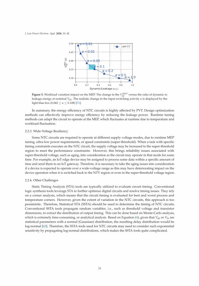
J. Low Power Electron. Appl. 2020, 10, 42
0.0 0.2 0.4 0.6 0.8 1.0Dynamic/Leakage (a.u.)
0.30
0.35
0.40
0.45
0.50
VMEP
dd(V
)
=0.01
=0.02
=0.05=0.1
=0.2=0.5 =1.0
c499 TT
Figure 5. Workload variation impact on the MEP. The change in the VMEPdd versus the ratio of dynamic to
leakage energy at nominal Vdd. The realistic change in the input switching activity α is displayed by thelight blue box (0.062 ≤ α ≤ 0.108) [71].
In summary, the energy efficiency of NTC circuits is highly affected by PVT. Design optimizationmethods can effectively improve energy efficiency by reducing the leakage power. Runtime tuningmethods can adapt the circuit to operate at the MEP, which fluctuates at runtime due to temperature andworkload fluctuation.
2.2.3. Wide-Voltage Resiliency
Some NTC circuits are required to operate at different supply voltage modes, due to runtime MEPtuning, ultra-low power requirements, or speed constraints (super-threshold). When a task with specifictiming constraints executes on the NTC circuit, the supply voltage may be increased to the super-thresholdregion to meet the performance constraints. However, this brings reliability issues associated withsuper-threshold voltage, such as aging, into consideration as the circuit may operate in that mode for sometime. For example, an IoT edge device may be assigned to process some data within a specific amount oftime and send them to an IoT gateway. Therefore, it is necessary to take the aging issues into considerationif a device is expected to operate over a wide-voltage range as this may have deteriorating impact on thedevice operation when it is switched back to the NTV region or even in the super-threshold voltage region.
2.2.4. Other Challenges
Static Timing Analysis (STA) tools are typically utilized to evaluate circuit timing. Conventionallogic synthesis tools leverage STA to further optimize digital circuits and resolve timing issues. They relyon a corner analysis, which means that the circuit timing is evaluated for best and worst process andtemperature corners. However, given the extent of variation in the NTC circuits, this approach is toopessimistic. Therefore, Statistical STA (SSTA) should be used to determine the timing of NTC circuits.Conventional SSTA tools propagate random variables, i.e., such as threshold voltage and transistordimensions, to extract the distribution of output timing. This can be done based on Monte-Carlo analysis,which is extremely time-consuming, or analytical analysis. Based on Equation (4), given that Vdd or Vth arestatistical parameters with a normal (Gaussian) distribution, the resulting delay distribution would belog-normal [43]. Therefore, the SSTA tools used for NTC circuits may need to consider such exponentialsensitivity by propagating log-normal distributions, which makes the SSTA tools quite complicated.
33
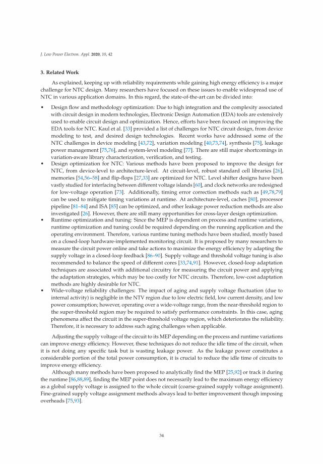
J. Low Power Electron. Appl. 2020, 10, 42
3. Related Work
As explained, keeping up with reliability requirements while gaining high energy efficiency is a majorchallenge for NTC design. Many researchers have focused on these issues to enable widespread use ofNTC in various application domains. In this regard, the state-of-the-art can be divided into:
• Design flow and methodology optimization: Due to high integration and the complexity associatedwith circuit design in modern technologies, Electronic Design Automation (EDA) tools are extensivelyused to enable circuit design and optimization. Hence, efforts have been focused on improving theEDA tools for NTC. Kaul et al. [33] provided a list of challenges for NTC circuit design, from devicemodeling to test, and desired design technologies. Recent works have addressed some of theNTC challenges in device modeling [43,72], variation modeling [40,73,74], synthesis [75], leakagepower management [75,76], and system-level modeling [77]. There are still major shortcomings invariation-aware library characterization, verification, and testing.
• Design optimization for NTC: Various methods have been proposed to improve the design forNTC, from device-level to architecture-level. At circuit-level, robust standard cell libraries [26],memories [54,56–58] and flip-flops [27,33] are optimized for NTC. Level shifter designs have beenvastly studied for interfacing between different voltage islands [60], and clock networks are redesignedfor low-voltage operation [73]. Additionally, timing error correction methods such as [49,78,79]can be used to mitigate timing variations at runtime. At architecture-level, caches [80], processorpipeline [81–84] and ISA [85] can be optimized, and other leakage power reduction methods are alsoinvestigated [26]. However, there are still many opportunities for cross-layer design optimization.
• Runtime optimization and tuning: Since the MEP is dependent on process and runtime variations,runtime optimization and tuning could be required depending on the running application and theoperating environment. Therefore, various runtime tuning methods have been studied, mostly basedon a closed-loop hardware-implemented monitoring circuit. It is proposed by many researchers tomeasure the circuit power online and take actions to maximize the energy efficiency by adapting thesupply voltage in a closed-loop feedback [86–90]. Supply voltage and threshold voltage tuning is alsorecommended to balance the speed of different cores [33,74,91]. However, closed-loop adaptationtechniques are associated with additional circuitry for measuring the circuit power and applyingthe adaptation strategies, which may be too costly for NTC circuits. Therefore, low-cost adaptationmethods are highly desirable for NTC.
• Wide-voltage reliability challenges: The impact of aging and supply voltage fluctuation (due tointernal activity) is negligible in the NTV region due to low electric field, low current density, and lowpower consumption; however, operating over a wide-voltage range, from the near-threshold region tothe super-threshold region may be required to satisfy performance constraints. In this case, agingphenomena affect the circuit in the super-threshold voltage region, which deteriorates the reliability.Therefore, it is necessary to address such aging challenges when applicable.
Adjusting the supply voltage of the circuit to its MEP depending on the process and runtime variationscan improve energy efficiency. However, these techniques do not reduce the idle time of the circuit, whenit is not doing any specific task but is wasting leakage power. As the leakage power constitutes aconsiderable portion of the total power consumption, it is crucial to reduce the idle time of circuits toimprove energy efficiency.
Although many methods have been proposed to analytically find the MEP [25,92] or track it duringthe runtime [86,88,89], finding the MEP point does not necessarily lead to the maximum energy efficiencyas a global supply voltage is assigned to the whole circuit (coarse-grained supply voltage assignment).Fine-grained supply voltage assignment methods always lead to better improvement though imposingoverheads [75,93].
34
J. Low Power Electron. Appl. 2020, 10, 42
Performance variations in the NTV region can be addressed by using conservative techniques suchas structural duplication, voltage and frequency margining [94]. However, such approaches can imposesignificant area and energy overhead. Moreover, the conservative timing margin will increase the idleperiod of the structures and potentially reduce the energy benefits of the NTC. Soft edge clocking [95,96]and body biasing [97] are two other well-known approaches to deal with process variation at NTC. Severalmethods have already been proposed [75,98], which incorporate synthesis techniques to improve thecircuit characteristics for NTC.
Dynamic input vector variation is another source of variation [99]. By applying different inputvectors, different parts of the circuits are activated, leading to different propagation delay from inputs tooutputs. There are so-called better-than-worst-case design techniques to improve circuit performance orenergy considering dynamic input vector variations [48–50]. In these approaches, the timing margin of thecircuit is reduced to a value smaller than the conservative worst-case margin, and possible timing errors aredetected and corrected on-the-fly to achieve error resiliency on top of improved performance and energy.However, traditional designs try to balance the circuit and hence there is a critical point called “path walls”in which reducing the delay beyond this point leads to a huge number of timing failures. In order toreduce timing errors, and hence further improving the efficiency of better-than-worst-case designs, re-timingtechniques to avoid path walls are introduced in the literature [51,52]. However, such techniques are noteffective in NTC because of the increased amount of timing errors.
For some circuits, such as ALU, there is a difference between the execution time of slow instructions(SI) and fast instructions (FI) due to dynamic input vector variation. Based on this fact, an aging-awareinstruction scheduling is proposed in [100,101] to execute each instruction group (FI or SI) with its ownspecialized functional units to improve lifetime.
In NTC, the delay difference between FI and SI is more pronounced. This means that if the clockcycle is set according to SI propagation delay, there is a considerable waste of leakage energy during theexecution of FIs. Based on this, we propose a technique in which the clock cycle is significantly reducedclose to the propagation delay of FI instructions to reduce the wasted leakage energy. In this approach, SIsare executed in multiple cycles to avoid possible timing failures.
At the super-threshold domain, various coarse-grained power-gating techniques have been proposedto turn-off idle cores [102–104]. The cores are turned-off when determined idle time is observed. However,such approaches require a state preservation mechanism and typically impose a long wake-up latency,which is costly at NTC. Furthermore, two methods based on the power-gating of execution units areproposed in [105]. These techniques allow the power gating of an entire execution unit. However, some ofthe instructions of an execution unit are utilized rarely by the running applications. Therefore, analyzingthe instruction utilization pattern could reveal opportunities for fine-grained power-gating.
4. Cross-Layer Data Path Optimization
4.1. Overview
To save leakage energy, it is important to reduce the time a circuit is powered on but idle, i.e., the timea circuit is performing no operation. For this purpose, the timing slack under all operation conditions hasto be trimmed. This is a very challenging task, in particular for functional units, which are fundamentalcomponents of data paths. In functional units, different operations have different timing criticalitiesand slacks. For instance, in an ALU, some operations need only a fraction of a clock cycle (e.g., logicoperations), whereas others require a full clock cycle (e.g., addition operation with operands of long datatype). Consequently, whenever an operation of the first category executed energy is “wasted” due toleakage, as the clock period is defined according to the slowest operation. Instead, it is much more efficient
35
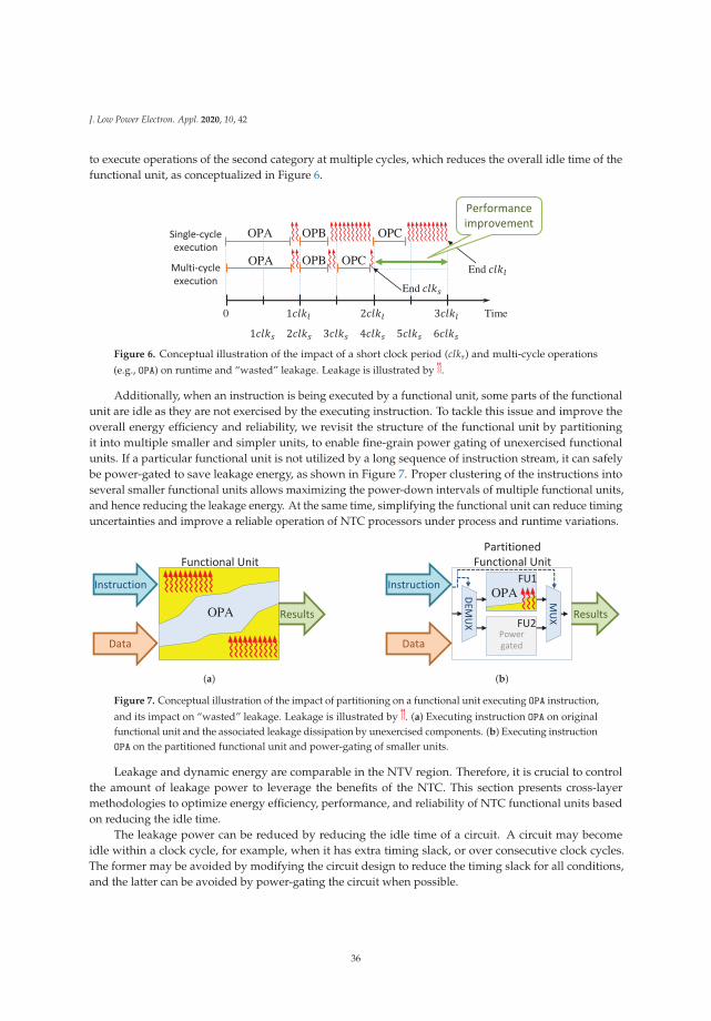
J. Low Power Electron. Appl. 2020, 10, 42
to execute operations of the second category at multiple cycles, which reduces the overall idle time of thefunctional unit, as conceptualized in Figure 6.
OPA OPB OPC
Time0
End
End
OPA OPB OPC
Figure 6. Conceptual illustration of the impact of a short clock period (clks) and multi-cycle operations
(e.g., OPA) on runtime and “wasted” leakage. Leakage is illustrated by .
Additionally, when an instruction is being executed by a functional unit, some parts of the functionalunit are idle as they are not exercised by the executing instruction. To tackle this issue and improve theoverall energy efficiency and reliability, we revisit the structure of the functional unit by partitioningit into multiple smaller and simpler units, to enable fine-grain power gating of unexercised functionalunits. If a particular functional unit is not utilized by a long sequence of instruction stream, it can safelybe power-gated to save leakage energy, as shown in Figure 7. Proper clustering of the instructions intoseveral smaller functional units allows maximizing the power-down intervals of multiple functional units,and hence reducing the leakage energy. At the same time, simplifying the functional unit can reduce timinguncertainties and improve a reliable operation of NTC processors under process and runtime variations.
OPA
(a)
OPA
(b)
Figure 7. Conceptual illustration of the impact of partitioning on a functional unit executing OPA instruction,
and its impact on “wasted” leakage. Leakage is illustrated by . (a) Executing instruction OPA on originalfunctional unit and the associated leakage dissipation by unexercised components. (b) Executing instructionOPA on the partitioned functional unit and power-gating of smaller units.
Leakage and dynamic energy are comparable in the NTV region. Therefore, it is crucial to controlthe amount of leakage power to leverage the benefits of the NTC. This section presents cross-layermethodologies to optimize energy efficiency, performance, and reliability of NTC functional units basedon reducing the idle time.
The leakage power can be reduced by reducing the idle time of a circuit. A circuit may becomeidle within a clock cycle, for example, when it has extra timing slack, or over consecutive clock cycles.The former may be avoided by modifying the circuit design to reduce the timing slack for all conditions,and the latter can be avoided by power-gating the circuit when possible.
36
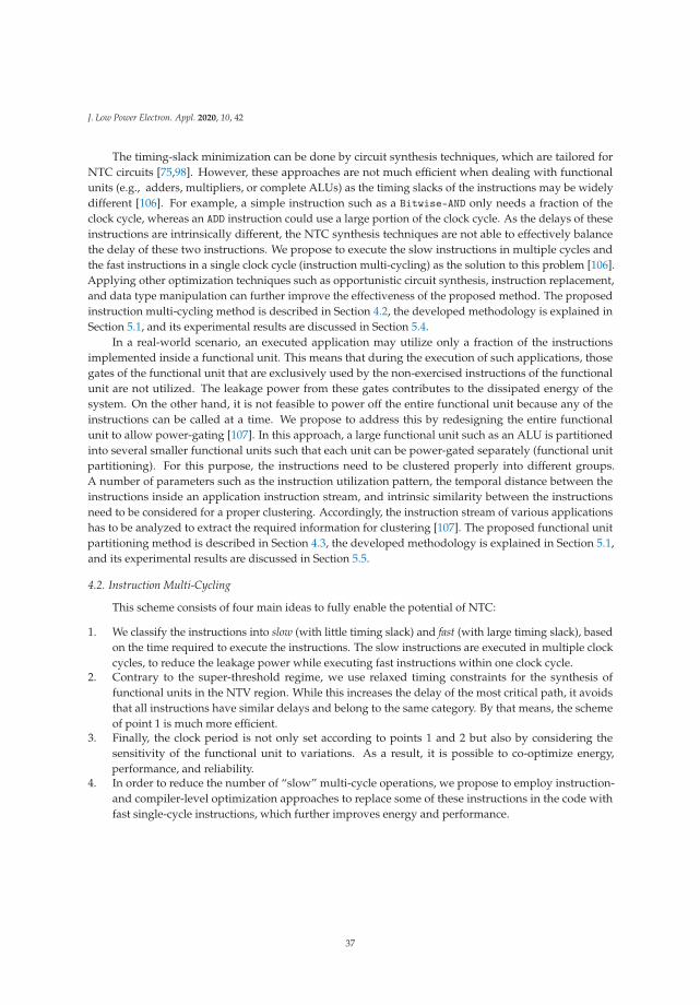
J. Low Power Electron. Appl. 2020, 10, 42
The timing-slack minimization can be done by circuit synthesis techniques, which are tailored forNTC circuits [75,98]. However, these approaches are not much efficient when dealing with functionalunits (e.g., adders, multipliers, or complete ALUs) as the timing slacks of the instructions may be widelydifferent [106]. For example, a simple instruction such as a Bitwise-AND only needs a fraction of theclock cycle, whereas an ADD instruction could use a large portion of the clock cycle. As the delays of theseinstructions are intrinsically different, the NTC synthesis techniques are not able to effectively balancethe delay of these two instructions. We propose to execute the slow instructions in multiple cycles andthe fast instructions in a single clock cycle (instruction multi-cycling) as the solution to this problem [106].Applying other optimization techniques such as opportunistic circuit synthesis, instruction replacement,and data type manipulation can further improve the effectiveness of the proposed method. The proposedinstruction multi-cycling method is described in Section 4.2, the developed methodology is explained inSection 5.1, and its experimental results are discussed in Section 5.4.
In a real-world scenario, an executed application may utilize only a fraction of the instructionsimplemented inside a functional unit. This means that during the execution of such applications, thosegates of the functional unit that are exclusively used by the non-exercised instructions of the functionalunit are not utilized. The leakage power from these gates contributes to the dissipated energy of thesystem. On the other hand, it is not feasible to power off the entire functional unit because any of theinstructions can be called at a time. We propose to address this by redesigning the entire functionalunit to allow power-gating [107]. In this approach, a large functional unit such as an ALU is partitionedinto several smaller functional units such that each unit can be power-gated separately (functional unitpartitioning). For this purpose, the instructions need to be clustered properly into different groups.A number of parameters such as the instruction utilization pattern, the temporal distance between theinstructions inside an application instruction stream, and intrinsic similarity between the instructionsneed to be considered for a proper clustering. Accordingly, the instruction stream of various applicationshas to be analyzed to extract the required information for clustering [107]. The proposed functional unitpartitioning method is described in Section 4.3, the developed methodology is explained in Section 5.1,and its experimental results are discussed in Section 5.5.
4.2. Instruction Multi-Cycling
This scheme consists of four main ideas to fully enable the potential of NTC:
1. We classify the instructions into slow (with little timing slack) and fast (with large timing slack), basedon the time required to execute the instructions. The slow instructions are executed in multiple clockcycles, to reduce the leakage power while executing fast instructions within one clock cycle.
2. Contrary to the super-threshold regime, we use relaxed timing constraints for the synthesis offunctional units in the NTV region. While this increases the delay of the most critical path, it avoidsthat all instructions have similar delays and belong to the same category. By that means, the schemeof point 1 is much more efficient.
3. Finally, the clock period is not only set according to points 1 and 2 but also by considering thesensitivity of the functional unit to variations. As a result, it is possible to co-optimize energy,performance, and reliability.
4. In order to reduce the number of “slow” multi-cycle operations, we propose to employ instruction-and compiler-level optimization approaches to replace some of these instructions in the code withfast single-cycle instructions, which further improves energy and performance.
37

J. Low Power Electron. Appl. 2020, 10, 42
4.2.1. Energy Improvement through Instruction Multi-Cycling
The propagation delay of functional units is typically dependent on input vectors. For example, inan ALU, the instructions can be categorized into slow instruction and fast instructions and the delay gapbetween fast and slow instructions might be significant. The logical operations such as inversion can beexecuted very fast while the execution of arithmetic operations such as addition and subtract requiresmore time. Figure 8a shows the normalized delay of various instructions of an ALU at 0.5 V (accordingto the simulation setup presented in Section 5). The synthesis tool balances as many paths as possible tooptimize the energy given the timing constraints. In this case, 26 instructions are balanced to be critical ornear-critical in terms of timing (slow instructions); however, the rest of the instructions require less timefor completion (fast instructions).
In a traditional design approach, the delay of the unit is determined by the delay of the slowestinstruction. Therefore, during the execution of the fast instructions, the ALU finishes the execution earlyand leaks for the rest of the clock cycle. The “dissipated” leakage energy is more important in the NTCbecause (1) the leakage energy is significant and constitutes a significant portion of the total energy, (2) thedelay gap between the fast instructions and the slow instructions is even more pronounced due to theimpact of process variation. As shown in Figure 8a, the amount of variation induced delay (the differencebetween the nominal delay and the worst-case delay) is larger for the slow instructions, which significantlyincrease the delay gap between the slow and fast instructions in the near-threshold regime.
38
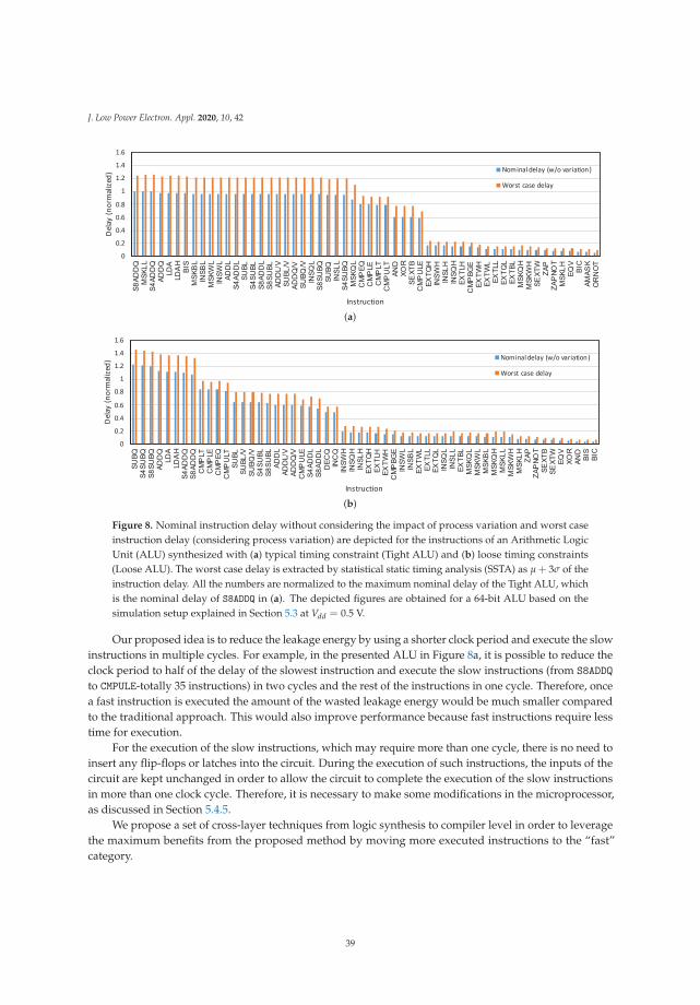
J. Low Power Electron. Appl. 2020, 10, 42
(a)
(b)
Figure 8. Nominal instruction delay without considering the impact of process variation and worst caseinstruction delay (considering process variation) are depicted for the instructions of an Arithmetic LogicUnit (ALU) synthesized with (a) typical timing constraint (Tight ALU) and (b) loose timing constraints(Loose ALU). The worst case delay is extracted by statistical static timing analysis (SSTA) as μ + 3σ of theinstruction delay. All the numbers are normalized to the maximum nominal delay of the Tight ALU, whichis the nominal delay of S8ADDQ in (a). The depicted figures are obtained for a 64-bit ALU based on thesimulation setup explained in Section 5.3 at Vdd = 0.5 V.
Our proposed idea is to reduce the leakage energy by using a shorter clock period and execute the slowinstructions in multiple cycles. For example, in the presented ALU in Figure 8a, it is possible to reduce theclock period to half of the delay of the slowest instruction and execute the slow instructions (from S8ADDQ
to CMPULE-totally 35 instructions) in two cycles and the rest of the instructions in one cycle. Therefore, oncea fast instruction is executed the amount of the wasted leakage energy would be much smaller comparedto the traditional approach. This would also improve performance because fast instructions require lesstime for execution.
For the execution of the slow instructions, which may require more than one cycle, there is no need toinsert any flip-flops or latches into the circuit. During the execution of such instructions, the inputs of thecircuit are kept unchanged in order to allow the circuit to complete the execution of the slow instructionsin more than one clock cycle. Therefore, it is necessary to make some modifications in the microprocessor,as discussed in Section 5.4.5.
We propose a set of cross-layer techniques from logic synthesis to compiler level in order to leveragethe maximum benefits from the proposed method by moving more executed instructions to the “fast”category.
39
J. Low Power Electron. Appl. 2020, 10, 42
4.2.2. Logic Synthesis for NTV Region
In order to show the impact of the logic synthesis on the ALU, we synthesized the same ALU withtwo different strategies. First, the ALU is synthesized with tight timing and area constraints, which is thedefault strategy in the super-threshold region. From now on, we refer to this synthesized ALU as TightALU. As the results depicted in Figure 8a show, the synthesis tool balanced the delay of many instructions(mostly arithmetic instructions) to maximize the energy efficiency and performance. However, thereare still many instructions (mostly logic instructions), which are too short to be balanced similar to theslow instructions. Furthermore, there is a sharp transition from the delay of slow instructions to the fastinstructions.
Then, the same ALU is synthesized with loose timing and area constraints (Loose ALU). The results ofthis synthesis are shown in Figure 8b. Since the synthesis tool is not under tight constraints, the delaysof the slow instructions are larger compared to the Tight ALU, and there is a smooth transition from thedelay of the slow instructions to the fast instructions.
In summary, the synthesis results based on the simulation setup presented in Section 5.3, show thatthe performance of the Tight ALU is better than the Loose ALU by 13% considering the variations; however,due to the wide spectrum of the delays of the instructions in the Loose ALU, there are more opportunitiesfor improving the ALU with the envisioned multi-cycling technique. The reason is that fewer instructionsare critical in terms of timing and by cleverly choosing the clock period we can gain in terms of energyand performance, as shown later in Section 5.
4.2.3. High-Level Optimization Techniques
From the above discussion, we observe that some ALU instructions are slower with longer executiontime, while other instructions are faster with shorter execution time. Therefore, the aim is to exploithigh-level optimization techniques such as data type conversion and instruction replacement to replaceslower instructions of an application by fast ones wherever possible, so that the overall energy demandwill be reduced further. Since the slower instructions are executed in multiple clock cycles, replacing themwith faster instruction can also improve the performance by reducing the Cycle Per Instruction of theapplications.
Data type conversion: The selection of data types for variables has a huge impact on the instructionbinary generated by the compiler. The data types such as short (1-byte), char (2-byte), int (4-byte) andlong (8-byte) not only specify the storage space size of variables but also the type of operation on thevariables (e.g., 64-bit arithmetic such as ADDQ vs. 32-bit arithmetic such as ADDL). This affects the occurrencerate of slower and faster instructions within an application. Hence, in addition to memory optimization,a clever data type selection will help to save energy by using fast instructions (e.g., ADDL in Figure 8b)instead of the slow ones (e.g., ADDQ in Figure 8b).
Instruction replacement: Many applications such as sorting and matrix multiplication algorithmsspend most of the execution time in loops. Hence, simple instructions such as increasing loop countersand array indexes significantly contribute to the overall instruction count. If such instructions are notassigned appropriate data type and operation, they can impose significant performance and energyoverhead. For instance, since modern ALUs have a dedicated increment/decrement circuitry, the usage ofincrement/decrement instructions plays a vital role in improving the performance and energy efficiencyby reducing the number of slower instructions. This and other instruction replacements (e.g., shift insteadof multiplication) can be achieved either by the programmer or using different compiler optimizationtechniques.
40
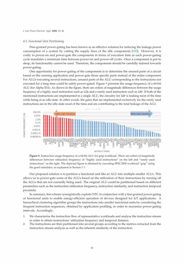
J. Low Power Electron. Appl. 2020, 10, 42
4.3. Functional Unit Partitioning
Fine-grained power-gating has been known as an effective solution for reducing the leakage powerconsumption of a system by cutting the supply lines of the idle components [105]. However, it iscostly to power-on and power-gate the components in terms of execution time as each power-gatingcycle mandates a minimum time between power-on and power-off cycles. Once a component is put tosleep, its functionality cannot be used. Therefore, the components should be carefully tailored towardspower-gating.
One opportunity for power-gating of the components is to determine the unused parts of a circuitbased on the running application and power-gate those specific parts instead of the entire component.For ALUs executing several instructions, unused parts of the ALU corresponding to the instructions notexecuted for a long time could be safely power-gated. Figure 9 presents the usage frequency of a 64-bitALU (for Alpha ISA). As shown in the figure, there are orders of magnitude differences between the usagefrequency of a highly used instruction such as LDA and a rarely used instruction such as ZAP. If both of thementioned instructions are implemented in a single ALU, the circuitry for ZAP is leaking most of the timewhile being at an idle state. In other words, the gates that are implemented exclusively for the rarely usedinstructions are in the idle state most of the time and are contributing to the total leakage of the ALU.
Figure 9. Instruction usage frequency in a 64-bit ALU for gzip workload. There are orders of magnitudedifferences between utilization frequency of “highly used instructions” on the left and “rarely usedinstructions” on the right. The depicted figure is obtained by executing SPEC2000 workload “gzip” usingthe gem5 simulator, as explained in Section 5.3.
Our proposed solution is to partition a functional unit like an ALU into multiple smaller ALUs. Thisallows us to power-gate some of the ALUs based on the utilization of their instructions by turning offthe ALUs that are not currently being used. The original ALU could be partitioned based on differentparameters such as the instruction utilization frequency, instruction similarity, and instruction temporalproximity.
In summary, this scheme synergistically exploits NTC in conjunction with a fine-grained power-gatingof functional units to enable energy-efficient operation of devices designed for IoT applications. Ahierarchical clustering algorithm groups the instructions into smaller functional units by considering thefrequent instruction sequences, obtained by application profiling, in order to maximize power-gatingintervals. Accordingly,
1. We characterize the instruction flow of representative workloads and analyze the instruction streamin order to obtain instructions’ utilization frequency and temporal distance.
2. The instructions are then partitioned into several groups according to the metrics extracted from theinstruction stream analysis as well as the inherent similarity of the instruction.
41
J. Low Power Electron. Appl. 2020, 10, 42
3. Each set of instructions residing in the same partition will be implemented by a dedicated functionalunit, and they form a complete functional unit altogether.
4. To reduce the leakage power, only the functional unit corresponding to the running instructionpartition is activated while other units are power-gated.
4.3.1. Instruction Pattern Analysis
A careful analysis of the instruction patterns on a set of representative workloads provides informationregarding the ALU partitioning. For this purpose, we first simulate the execution of a set of representativeworkloads by an architectural simulation tool as explained in Section 5, and then based on the extractedinstruction streams the utilization frequency and the temporal distance of different instructions areextracted.
Instruction utilization frequency: The instruction utilization frequencies presented in Figure 9 showa significant difference in utilization among the instructions. The instruction utilization frequency hasan inverse relation with the power-gating feasibility for the ALUs associated with the instructions. Forexample, the ALUs that contain instructions ADDQ and BIS are less likely to be power-gated because theseinstructions appear in the instruction buffer on average every 10 cycles. However, it is more likely topower-gate the ALUs implementing the rarely used instructions on the right side of Figure 9 such asS8ADDL.
The utilization frequency of an instruction can be simply defined as the number of cycles in whichthe instruction is executed divided by total cycles. For a given instruction stream S, which is a sequencecontaining N = |S| instructions, we can define the frequency of instruction A as:
FreqA =#Si ∈ S such that Si = A
N(5)
where Si is the i-th element (instruction) of S. If an instruction is used rarely, it can be easily groupedinto any existing ALUs. However, we need to be more cautious in grouping frequently used instructionbecause the grouping strategy might improve or deteriorate the power-gating capability of the ALUs.Based on this analysis, we can define the frequency distance metric between two instructions A and B asthe geometric mean:
dist f reqA-B =
√FreqA ∗ FreqB. (6)
Such definition facilitates the partitioning of rarely used instructions into a single ALU.Instruction temporal distance: Some instructions are more likely to appear next to each other in an
application. For example, from “bzip2” workload, we observed that ADDL appears after LDA on averageevery 2.97 instructions (see Figure 10). In these cases, it could be beneficial to group these neighboringinstructions inside one ALU in order to improve the power-gating interval for other ALUs.
The temporal distance between two instructions A and B can be extracted based on the number ofcycles between any occurrences of A and B. For example, according to the results presented in Figure 10,there are 19146 LDA instructions that are directly followed by an ADDL instruction, and there are 11860 LDA
instructions that are followed by an ADDL instruction after three cycles. Based on the workload analysis,a distribution is extracted for every instruction pair A-B, which explains the percentage of the A-B pairsthat are far from each other by k cycles. The Survival Function (SF) (defined as 1 − CDF of a distribution)of these temporal distance distributions is useful in the clustering problem definition in Section 4.3.2.
We define a temporal distance set which contains the indexes of consequent instructions A and B andtheir corresponding distances (i, k):
TemporalA-B ={(i, k)
∣∣ 0 < i, 0 < k, Si = A, Si+k = B,�j, 0 < j < k, Si+j ∈ {A, B}}. (7)
42
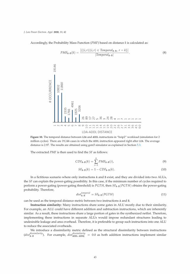
J. Low Power Electron. Appl. 2020, 10, 42
Accordingly, the Probability Mass Function (PMF) based on distance k is calculated as:
PMFA-B(k) =
∣∣{(i, r)|(i, r) ∈ TemporalA-B, r = k}∣∣
|TemporalA-B| . (8)19
146
1083
211
860
2335
1766
4961
1925 32
0626 89 17 27 5 36 3 24 28 4 1 7 1 1 1 1 1
1 2 3 4 5 6 7 8 9 10 11 12 13 14 15 19 20 22 26 27 31 33 36 45 60
# O
CCUR
RENC
E
LDA-ADDL DISTANCEFigure 10. The temporal distance between LDA and ADDL instructions in “bzip2” workload (simulation for 2million cycles). There are 19,146 cases in which the ADDL instruction appeared right after LDA. The averagedistance is 2.97. The results are obtained using gem5 simulator as explained in Section 5.3.
The extracted PMF is then used to find the SF as follows:
CDFA-B(k) =k
∑i=1
PMFA-B(i), (9)
SFA-B(k) = 1 − CDFA-B(k). (10)
In a fictitious scenario where only instructions A and B exist, and they are divided into two ALUs,the SF can explain the power-gating possibility. In this case, if the minimum number of cycles required toperform a power-gating (power-gating threshold) is PGTH, then SFA-B(PGTH) obtains the power-gatingprobability. Therefore,
disttemporalA-B = SFA-B(PGTH) (11)
can be used as the temporal distance metric between two instructions A and B.Instruction similarity: Many instructions share some gates in ALU mostly due to their similarity.
For example, an ALU could have different addition and subtraction instructions, which are inherentlysimilar. As a result, these instructions share a large portion of gates in the synthesized netlist. Therefore,implementing these instructions in separate ALUs would impose redundant structures leading toundesirable leakage and area overhead. Therefore, it is preferable to group such instructions into one ALUto reduce the associated overheads.
We introduce a dissimilarity metric defined as the structural dissimilarity between instructions(distdissimilarity
A-B ). For example, distdissimilarityADDL-ADDQ = 0.0 as both addition instructions implement similar
43
J. Low Power Electron. Appl. 2020, 10, 42
functionality. However, distdissimilarityADDL-ORNOT = 1.0 as the corresponding instructions implement two completely
different logic structures. The dissimilarity values are assigned based on the knowledge we have about thelogic implementation of different instructions.
Some of the above parameters may lead to contradictory grouping of instructions into ALUs.For example, instructions S8ADDL and ADDL should be grouped into one ALU because of inherent similarity;however, according to their utilization frequencies they should be placed into different ALUs to allowpower-gating. In the next section, we define a formal clustering problem considering the aforementionedparameters and solve it to find the best instruction grouping strategy.
4.3.2. Instruction Clustering Problem Definition
The problem of partitioning a large ALU into smaller ALUs can be defined as a clustering problem,in which the distance between the instructions is explained by temporal proximity, utilization frequency,and similarity of instructions. The goal of such clustering algorithm is to maximize the distance betweenALUs while minimizing the distance between instructions of each ALU. This allows us to increase theoverall power-gating likelihood of ALUs, which leads to lower leakage and better energy efficiency.
For this purpose we apply the Agglomerative Hierarchical Clustering (AHC) algorithm [108] tocluster the instructions into several groups, each group implemented in one ALU. AHC is suitable for ourproblem because we can provide pairwise distances between each and every two instructions.
We create the pairwise distance matrix needed for the AHC algorithm based on the frequency distancemetric (dist f req
A-B ), temporal distance metric (disttemporalA-B ), and structural similarity (distsimilarity
A-B ) introduced inthe previous section. Finally, the elements of the pairwise distance matrix (pdist) are obtained as (Cartesiandistance on a 3D space):
pdist2A-B = (β.dist f req
A-B )2 + (γ.disttemporal
A-B )2 + (λ.distdissimilarityA-B )2. (12)
Here, β, γ, λ are coefficients to scale all the metrics into the same scale.We consider the single-linkage clustering method on the AHC. In a single-linkage method, the linkage
function D(X, Y), which is the distance between two clusters X and Y, is defined as the minimum distancebetween every two members of the clusters:
D(X, Y) = minA∈X,B∈Y
pdistA-B. (13)
Therefore, maximizing the distance between clusters X and Y will allow the maximum power gatingpossibility of the corresponding ALU implementations and improves the energy efficiency.
4.3.3. Fine-Grained Power-Gating Prediction
Once the inactive phase for a component is detected at architecture-level, the component can bepower-gated by asserting a sleep signal on the header/footer sleep transistors. Although the power-gatingcan effectively reduce the wasted leakage energy, it has to be done when the functional unit is not utilizedfor a minimum number of cycles (PGTH) to break-even the associated overheads. This value is estimatedto be around 10 cycles for a typical technology [105,109].
The inactive phase of a functional unit can be predicted based on several techniques at runtime. Inorder to determine the inactive interval of each functional unit and decide whether to power gate it or not,it is possible to monitor the instruction buffer for a number of upcoming instructions while considering thebranch prediction buffer. However, the power-gating signal for a given functional unit can be mispredicteddue to branch misprediction. As a result of misprediction, the entire pipeline may be needed to be flushed
44
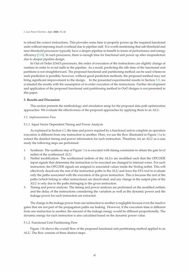
J. Low Power Electron. Appl. 2020, 10, 42
to reload the correct instructions. This provides some time to properly power up the required functionalunits without imposing much overhead due to pipeline stall. It is worth mentioning that sub-threshold andnear-threshold processors typically have a deeper pipeline to benefit in terms of performance and energyefficiency [110]. In such processors, there is enough time for functional unit power up after mispredictiondue to deeper pipeline design.
In Out of Order (OoO) processors, the order of execution of the instructions can slightly change atruntime in order to avoid stalls in the pipeline. As a result, predicting the idle time of the functional unitpartitions is not straightforward. The proposed functional unit partitioning method can be used wheneversuch prediction is possible; however, without good prediction methods, the proposed method may notbring significant improvement to the design. In the presented experimental results in Section 5.5, weevaluated the results with the assumption of in-order execution of the instructions. Further developmentand application of the proposed functional unit partitioning method to OoO designs is not presented inthis paper.
5. Results and Discussion
This section presents the methodology and simulation setup for the proposed data path optimizationapproaches. We evaluate the effectiveness of the proposed approaches by applying them to an ALU.
5.1. Implementation Flow
5.1.1. Input Vector Dependent Timing and Power Analysis
As explained in Section 4.2, the time and power required by a functional unit to complete an operationexecution is different from one instruction to another. Here, we use the flow illustrated in Figure 11a toextract the detailed timing and power information for each instruction. Therefore, for an ALU as a casestudy the following steps are performed:
1. Synthesis: The synthesis step of Figure 11a is executed with timing constraints to obtain the gate levelnetlist of the synthesized ALU.
2. Netlist modification: The synthesized netlists of the ALUs are modified such that the OPCODEinput signals that determine the instruction to be executed are changed to internal wires. For eachinstruction, the OPCODE signals are assigned to associated values inside the Verilog netlist. This willeffectively deactivate the rest of the instruction paths in the ALU and force the STA tool to evaluateonly the paths associated with the execution of the given instruction. This is because the rest of thepaths (which belong to other instructions) are deactivated, and any change in the output pins of theALU is only due to the paths belonging to the given instruction.
3. Timing and power analysis: The timing and power analyses are performed on the modified netlists,and the delay of the instructions considering the variation as well as the dynamic power and theleakage power for each instruction are extracted.
The change in the leakage power from one instruction to another is negligible because even the inactivegates that are not part of the propagation paths are leaking. However, if the execution time is differentfrom one instruction to another, the amount of the leakage energy would be different proportionally. Thedynamic energy for each instruction is also calculated based on the dynamic power value.
5.1.2. Functional Unit Partitioning Flow
Figure 11b shows the overall flow of the proposed functional unit partitioning method applied to anALU. The flow consists of three distinct steps:
45
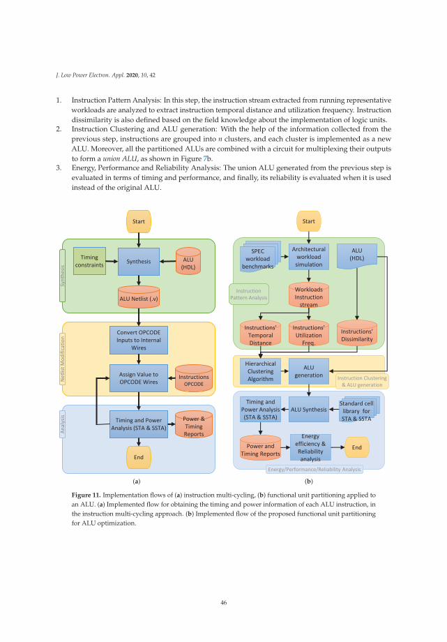
J. Low Power Electron. Appl. 2020, 10, 42
1. Instruction Pattern Analysis: In this step, the instruction stream extracted from running representativeworkloads are analyzed to extract instruction temporal distance and utilization frequency. Instructiondissimilarity is also defined based on the field knowledge about the implementation of logic units.
2. Instruction Clustering and ALU generation: With the help of the information collected from theprevious step, instructions are grouped into n clusters, and each cluster is implemented as a newALU. Moreover, all the partitioned ALUs are combined with a circuit for multiplexing their outputsto form a union ALU, as shown in Figure 7b.
3. Energy, Performance and Reliability Analysis: The union ALU generated from the previous step isevaluated in terms of timing and performance, and finally, its reliability is evaluated when it is usedinstead of the original ALU.
(a) (b)
Figure 11. Implementation flows of (a) instruction multi-cycling, (b) functional unit partitioning applied toan ALU. (a) Implemented flow for obtaining the timing and power information of each ALU instruction, inthe instruction multi-cycling approach. (b) Implemented flow of the proposed functional unit partitioningfor ALU optimization.
46
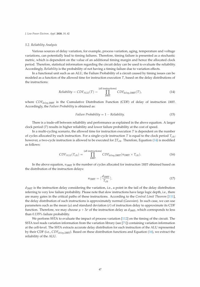
J. Low Power Electron. Appl. 2020, 10, 42
5.2. Reliability Analysis
Various sources of delay variation, for example, process variation, aging, temperature and voltagevariations, can potentially lead to timing failures. Therefore, timing failure is presented as a stochasticmetric, which is dependent on the value of an additional timing margin and hence the allocated clockperiod. Therefore, statistical information regarding the circuit delay can be used to evaluate the reliability.Accordingly, Reliability is the probability of not having a timing failure due to variation effects.
In a functional unit such as an ALU, the Failure Probability of a circuit caused by timing issues can bemodeled as a function of the allowed time for instruction execution T, based on the delay distributions ofthe instructions:
Reliability = CDFALU(T) ={all instructions}
∏INST
CDFdelay,INST(T), (14)
where CDFdelay,INST is the Cumulative Distribution Function (CDF) of delay of instruction INST.Accordingly, the Failure Probability is obtained as:
Failure Probability = 1 − Reliability. (15)
There is a trade-off between reliability and performance as explained in the above equation. A largerclock period (T) results in higher reliability and lower failure probability at the cost of speed.
In a multi-cycling scenario, the allowed time for instruction execution T is dependent on the numberof cycles allocated by each instruction. For a single-cycle instruction T is equal to the clock period Tclk;however, a two-cycle instruction is allowed to be executed for 2Tclk. Therefore, Equation (14) is modifiedas follows:
CDFALU(Tclk) ={all instructions}
∏INST
CDFdelay,INST(nINST × Tclk). (16)
In the above equation, nINST is the number of cycles allocated for instruction INST obtained based onthe distribution of the instruction delays:
nINST = �dINSTTclk
�. (17)
dINST is the instruction delay considering the variation, i.e., a point in the tail of the delay distributionreferring to very low failure probability. Please note that slow instructions have large logic depth, i.e., thereare many gates in the critical paths of these instructions. According to the Central Limit Theorem [111],the delay distribution of such instructions is approximately normal (Gaussian). In such case, we can useparameters such as the mean (μ) and standard deviation (σ) of instruction delay to approximate its CDFfunction. Therefore, we may choose μ + 3σ of the instruction delay as dINST, which corresponds to lessthan 0.135% failure probability.
We perform SSTA to evaluate the impact of process variation [112] on the timing of the circuit. TheSSTA tool reads variation information from the variation library (see [71]) containing variation informationat the cell-level. The SSTA extracts accurate delay distribution for each instruction of the ALU representedby their CDF (i.e., CDFdelay,INST). Based on these distribution functions and Equation (16), we extract thereliability of the ALU.
47
J. Low Power Electron. Appl. 2020, 10, 42
5.3. Simulation Setup
The proposed approaches are applied to a 64-bit ALU, namely the ALU of the Illinois Verilog Model(IVM) [113], which is a Verilog model for the Alpha 21264 core. The selected ALU implements 64-bit RISCInstruction Set Architecture of Alpha processor. For this purpose, we synthesize the HDL from the IVMALU with loose and tight timing constraints and characterize it for the NTC by an SSTA to extract thepower and delay of each instruction as well as the reliability as explained in Section 5.1. The synthesis isdone using the Synopsys Design Compiler [114]. Statistical static timing analysis (SSTA) is done using aCadence Encounter Timing System [115], which is able to perform SSTA using statistical CCS or ECSMstandard cell library models [116].
In order to prepare such statistical standard cell libraries for timing and power analysis, the cells fromselected libraries [117,118] from 32 nm down to 10 nm are re-characterized using the Cadence VirtuosoVariety [119] and the cells that are not suitable for NTC are excluded from the library [33]. The Varietytool characterizes the cells considering the process variation and all the power and delay values are storedin the generated standard cell libraries. The process of library characterization can be time consuming.However, this is only done once and the obtained libraries can be used in different projects.
The SSTA performed by this method is applicable to the NTV region, because it can consider a skeweddelay model for the cells. Each SSTA timing analysis run takes more execution time compared to a simplerSTA run, which is typically done at nominal supply voltage ranges. Nevertheless, it is still much fastercompared to a Monte-Carlo-based SSTA. The same method is applied to synthesize and analyze thepartitioned ALUs generated by the functional unit partitioning method.
Additionally, we extract the instruction stream for SPEC2000 benchmark workloads using a gem5architectural simulator [120]. This is done by executing the workloads using gem5, fast forwardingto the start of the executed workloads, and collecting all the executed instructions and the providedoperands. The result of the architectural simulation is used to evaluate the impact of the proposedinstruction multi-cycling approach and to perform instruction pattern analysis and clustering in theproposed functional unit partitioning approach. The results of both approaches are compared to thebaseline, which is an IVM ALU that is synthesized with conventional tight timing constraints.
5.4. ALU Multi-Cycling Results
5.4.1. Multi-Cycling Improvement
By reducing the clock period below the delay of the slowest instruction, some instructions need tobe executed in multiple clock cycles. The number of the required clock cycles can be calculated fromEquation (17). The delay of the slowest instruction is 146 ns; hence, the minimum clock period for runningall instructions in one cycle is also 146 ns.
We changed the clock period of the Loose ALU and extracted the instructions, which should beexecuted in multiple cycles for each clock period. Here, the clock period is swept from 49 ns (one-thirdof the delay of the most critical instruction) to 100 ns to explain the impact of clock period on the circuitcharacteristics. As shown in Figure 12a, some instructions need to be executed in three cycles when theclock period is below 73 ns (which is half the delay of the most critical instruction—marked by a verticaldashed line in the figure).
The energy and performance improvement of the ALU executing workload “equake” are plottedin Figure 12b for various clock periods. The improvement numbers are calculated in comparison withthe Tight ALU, which executes all instructions in one clock cycle. When the clock period is reduced,the energy and performance improvements increase because the delay slacks of the instructions aretrimmed. However, when any change in the sets of 1-cycle, 2-cycle or 3-cycle instructions happens due
48
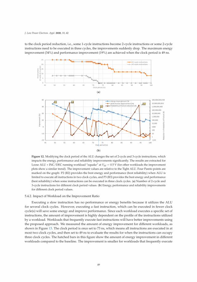
J. Low Power Electron. Appl. 2020, 10, 42
to the clock period reduction, i.e., some 1-cycle instructions become 2-cycle instructions or some 2-cycleinstructions need to be executed in three cycles, the improvements suddenly drop. The maximum energyimprovement (34%) and performance improvement (19%) are achieved when the clock period is 49 ns.
0
5
10
15
20
25
45 50 55 60 65 70 75 80 85 90 95 100
# in
ctru
ctio
ns
(2-c
ycle
s & 3
-cyc
les)
Clock period (ns)
# 2-cycle instructions# 3-cycle inctructions
(a)
(b)
Figure 12. Modifying the clock period of the ALU changes the set of 2-cycle and 3-cycle instructions, whichimpacts the energy, performance and reliability improvements significantly. The results are extracted forLoose ALU + INC/DEC running workload “equake” at Vdd = 0.5 V (for other workloads the improvementplots show a similar trend). The improvement values are relative to the Tight ALU. Four Pareto points aremarked on the graph: P2 (R2) provides the best energy and performance (best reliability) when ALU islimited to execute all instructions in two clock cycles, and P3 (R3) provides the best energy and performance(best reliability) when some instructions can be executed in three clock cycles. (a) Number of 2-cycle and3-cycle instructions for different clock period values. (b) Energy, performance and reliability improvementsfor different clock period values.
5.4.2. Impact of Workload on the Improvement Ratio
Executing a slow instruction has no performance or energy benefits because it utilizes the ALUfor several clock cycles. However, executing a fast instruction, which can be executed in fewer clockcycle(s) will save some energy and improve performance. Since each workload executes a specific set ofinstructions, the amount of improvement is highly dependent on the profile of the instructions utilizedby a workload. Workloads that frequently execute fast instructions will have better improvements usingthe proposed approach. We measured the amount of energy improvement for different workloads, asshown in Figure 13. The clock period is once set to 73 ns, which means all instructions are executed in atmost two clock cycles, and then set to 49 ns to evaluate the results for when the instructions can occupythree clock cycles. The hatched bars in this figure show the amount of energy improvement in differentworkloads compared to the baseline. The improvement is smaller for workloads that frequently execute
49
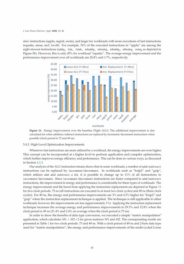
J. Low Power Electron. Appl. 2020, 10, 42
slow instructions (applu, mgrid, swim), and larger for workloads with more executions of fast instructions(equake, mesa, mcf, twolf). For example, 76% of the executed instructions in “applu” are among theeight slowest instructions (addq, lda, ldah, s4addq, s4subq, s8addq, s8subq, subq, as depicted inFigure 8b). However, this is only 45% for workload “equake”. The average energy improvement and theperformance improvement over all workloads are 20.8% and 1.7%, respectively.
0.00
5.00
10.00
15.00
20.00
25.00
30.00
35.00
40.00
45.00
ener
gy im
prov
emen
t (%
)
workloads
Loose ALU (T=49ns) Inst. Replacement (T=49ns)
Loose ALU (T=73ns) Inst. Replacement (T=73ns)
Figure 13. Energy improvement over the baseline (Tight ALU). The additional improvement is alsocalculated for when addition/subtract instructions are replaced by increment/decrement instructions whenpossible (clock period is 73 and 49 ns).
5.4.3. High-Level Optimization Improvements
Whenever fast instructions are more utilized by a workload, the energy improvements are even higher.This concept can be incorporated at a higher level to perform application and compiler optimization,which further improves energy efficiency and performance. This can be done in various ways, as discussedin Section 4.2.3.
Our analysis of the ALU instruction stream shows that in some workloads, a number of add/subtractinstructions can be replaced by increment/decrement. In workloads such as “bzip2” and “gzip”,which utilizes add and subtract a lot, it is possible to change up to 11% of all instructions toincrement/decrement. Since increment/decrement instructions are faster compared to add/subtract
instructions, the improvement in energy and performance is considerable for these types of workloads. Theenergy improvements and the boost from applying the instruction replacement are depicted in Figure 13for two clock periods: 73 ns (all instructions are executed in at most two clock cycles) and 49 ns (three clockcycles). For 49 ns, the energy and performance improvements are 3% and 4.3% higher for “bzip2” and“gzip” when the instruction replacement technique is applied. The technique is still applicable to otherworkloads; however, the improvements are less (approximately 1%). Applying the instruction replacementtechnique increases the average energy and performance improvements to 29.3% and 12.8% when theclock period is 49 ns (21.4% and 2.4% on average when the clock period is 73 ns).
In order to show the benefits of data type conversion, we executed a simple “matrix manipulation”application, which calculates M1 + M2 ∗ 2 for given matrices M1 and M2. The corresponding results arepresented in Table 1 for two clock periods: 73 and 49 ns. With a clock period of 49 ns and 2-byte data typeused for “matrix manipulation”, the energy and performance improvements of the multi-cycled Loose
50
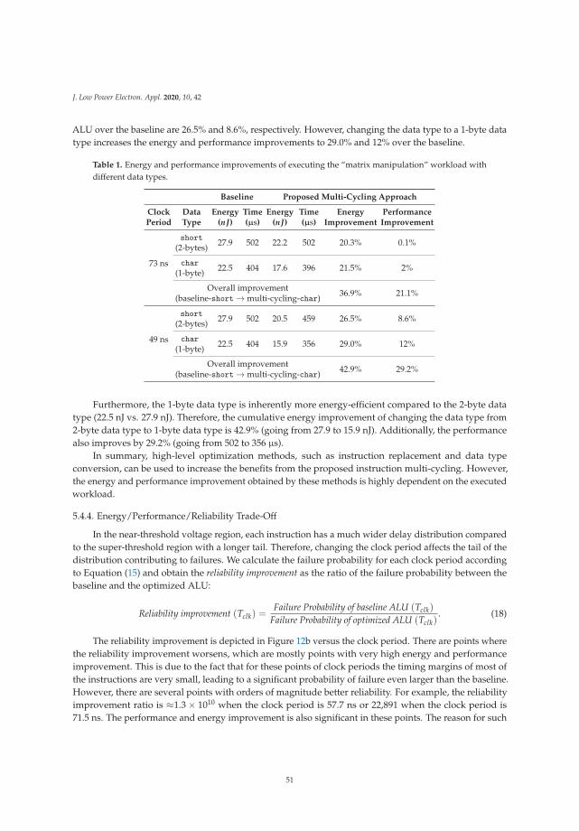
J. Low Power Electron. Appl. 2020, 10, 42
ALU over the baseline are 26.5% and 8.6%, respectively. However, changing the data type to a 1-byte datatype increases the energy and performance improvements to 29.0% and 12% over the baseline.
Table 1. Energy and performance improvements of executing the “matrix manipulation” workload withdifferent data types.
Baseline Proposed Multi-Cycling Approach
ClockPeriod
DataType
Energy(nJ)
Time(μs)
Energy(nJ)
Time(μs)
EnergyImprovement
PerformanceImprovement
73 ns
short(2-bytes) 27.9 502 22.2 502 20.3% 0.1%
char(1-byte) 22.5 404 17.6 396 21.5% 2%
Overall improvement(baseline-short → multi-cycling-char) 36.9% 21.1%
49 ns
short(2-bytes) 27.9 502 20.5 459 26.5% 8.6%
char(1-byte) 22.5 404 15.9 356 29.0% 12%
Overall improvement(baseline-short → multi-cycling-char) 42.9% 29.2%
Furthermore, the 1-byte data type is inherently more energy-efficient compared to the 2-byte datatype (22.5 nJ vs. 27.9 nJ). Therefore, the cumulative energy improvement of changing the data type from2-byte data type to 1-byte data type is 42.9% (going from 27.9 to 15.9 nJ). Additionally, the performancealso improves by 29.2% (going from 502 to 356 μs).
In summary, high-level optimization methods, such as instruction replacement and data typeconversion, can be used to increase the benefits from the proposed instruction multi-cycling. However,the energy and performance improvement obtained by these methods is highly dependent on the executedworkload.
5.4.4. Energy/Performance/Reliability Trade-Off
In the near-threshold voltage region, each instruction has a much wider delay distribution comparedto the super-threshold region with a longer tail. Therefore, changing the clock period affects the tail of thedistribution contributing to failures. We calculate the failure probability for each clock period accordingto Equation (15) and obtain the reliability improvement as the ratio of the failure probability between thebaseline and the optimized ALU:
Reliability improvement (Tclk) =Failure Probability of baseline ALU (Tclk)
Failure Probability of optimized ALU (Tclk). (18)
The reliability improvement is depicted in Figure 12b versus the clock period. There are points wherethe reliability improvement worsens, which are mostly points with very high energy and performanceimprovement. This is due to the fact that for these points of clock periods the timing margins of most ofthe instructions are very small, leading to a significant probability of failure even larger than the baseline.However, there are several points with orders of magnitude better reliability. For example, the reliabilityimprovement ratio is ≈1.3 × 10¹⁰ when the clock period is 57.7 ns or 22,891 when the clock period is71.5 ns. The performance and energy improvement is also significant in these points. The reason for such
51
J. Low Power Electron. Appl. 2020, 10, 42
large reliability improvements is that the baseline has many critical or near-critical instructions with zeroor minimal slack. However, the multi-cycling strategy is able to provide enough timing margin for manyinstructions such that the provided time for the execution of each instruction marks very high sigma valueson the tails of all the delay distributions. Therefore, the designer is able to find a good trade-off amongenergy efficiency, performance and reliability according to the design requirements.
5.4.5. Discussion
It is evident from the results analyzed before that the multi-cycling approach can provide considerableenergy and performance benefits, as well as reliability improvements. However, these results representthe ideal case where the clock period can be adjusted without any constraints.
In a real processor (or an ASIC), there may be other timing critical components, limiting the freedomfor modifying the clock period. Hence, another operation point in Figure 12b might be chosen. In suchscenarios, the entire processor has to operate at a higher frequency in order to exploit a short clock periodfor the ALU. This may require additional design tweaks for other parts of the processor. For this purpose,timing critical components of the processor can be split up into multiple “short-cycle” components.Consequently, this results in a deeper pipeline, requiring more control logic and more registers. However,this overhead should be compensated by the overall leakage savings of the entire processor due to theruntime benefits of our novel multi-cycling approach. In case a multi-cycle instruction has to be executed bythe ALU, the pipeline frontend of the microprocessor is stopped (through using a no-operation instruction,or clock gating), such that the ALU can work for multiple cycles without change of the input vector.
An alternative solution is to execute multiple short instructions in the ALU per clock cycle. By thatmeans, no major modifications of other processor components are necessary. For instance, to execute twoinstructions in a clock cycle, the high and low levels of the clock signal can be exploited as it was done inthe Intel Pentium 4 [121]. Executing more than two instructions in one cycle requires additional shiftedclock signals. Therefore, this scheme is only feasible for processors featuring reservation stations to executemultiple instructions per clock cycle.
In an energy efficient design, the operands of a functional unit are loaded from the memory before thefunctional unit starts executing the instruction, in order to improve power consumption and performance.These operands are typically stored in the local registers, which are easily accessible by the functional unitwithout much latency. As an example, the registers at the I/O of an ALU in a pipelined processor store theoperands used by the ALU.
5.5. Functional Unit Partitioning Results
This section presents the results of applying the proposed functional unit partitioning to an ALU,based on the simulation setup presented in Section 5.3.
5.5.1. Clustering Results
The distance metrics are extracted based on the analysis of the SPEC benchmark workloads.The temporal distance metric is extracted for PGTH = 100. The dendrogram in Figure 14 illustratesthe results of the AHC method. As shown in this figure, most of the rarely used instructions in Figure 9are either grouped together or grouped with other closely similar structures. The original ALU can bepartitioned into n smaller ALUs according to the dendrogram. One can determine the best n value, basedon inconsistency coefficients [122]. However, as the overhead of hardware implementation increases withthe number of clusters, we only have to limit n to have at most four clusters (ALUs). Here, we presentresults for partitioning the ALU into three and four smaller ALUs as the energy improvement for twoALUs vanishes away as the power-gating threshold (PGTH) increases.
52
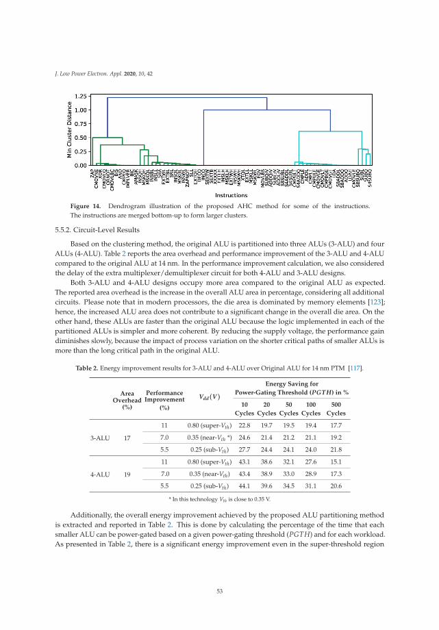
J. Low Power Electron. Appl. 2020, 10, 42
Figure 14. Dendrogram illustration of the proposed AHC method for some of the instructions.The instructions are merged bottom-up to form larger clusters.
5.5.2. Circuit-Level Results
Based on the clustering method, the original ALU is partitioned into three ALUs (3-ALU) and fourALUs (4-ALU). Table 2 reports the area overhead and performance improvement of the 3-ALU and 4-ALUcompared to the original ALU at 14 nm. In the performance improvement calculation, we also consideredthe delay of the extra multiplexer/demultiplexer circuit for both 4-ALU and 3-ALU designs.
Both 3-ALU and 4-ALU designs occupy more area compared to the original ALU as expected.The reported area overhead is the increase in the overall ALU area in percentage, considering all additionalcircuits. Please note that in modern processors, the die area is dominated by memory elements [123];hence, the increased ALU area does not contribute to a significant change in the overall die area. On theother hand, these ALUs are faster than the original ALU because the logic implemented in each of thepartitioned ALUs is simpler and more coherent. By reducing the supply voltage, the performance gaindiminishes slowly, because the impact of process variation on the shorter critical paths of smaller ALUs ismore than the long critical path in the original ALU.
Table 2. Energy improvement results for 3-ALU and 4-ALU over Original ALU for 14 nm PTM [117].
AreaOverhead
(%)
PerformanceImprovement
(%)
Vdd(V)
Energy Saving for
Power-Gating Threshold (PGT H) in %
10
Cycles
20
Cycles
50
Cycles
100
Cycles
500
Cycles
3-ALU 17
11 0.80 (super-Vth) 22.8 19.7 19.5 19.4 17.7
7.0 0.35 (near-Vth *) 24.6 21.4 21.2 21.1 19.2
5.5 0.25 (sub-Vth) 27.7 24.4 24.1 24.0 21.8
4-ALU 19
11 0.80 (super-Vth) 43.1 38.6 32.1 27.6 15.1
7.0 0.35 (near-Vth) 43.4 38.9 33.0 28.9 17.3
5.5 0.25 (sub-Vth) 44.1 39.6 34.5 31.1 20.6
* In this technology Vth is close to 0.35 V.
Additionally, the overall energy improvement achieved by the proposed ALU partitioning methodis extracted and reported in Table 2. This is done by calculating the percentage of the time that eachsmaller ALU can be power-gated based on a given power-gating threshold (PGTH) and for each workload.As presented in Table 2, there is a significant energy improvement even in the super-threshold region
53
J. Low Power Electron. Appl. 2020, 10, 42
(Vdd = 0.80 V). The reason is that one of the partitioned ALUs is mostly in sleep mode because itsinstructions are rarely used (see Figures 9 and 14). The percentage of the time an ALU is power-gated for aspecific PGTH is the same for all supply voltages; however, the energy improvement by the proposedALU partitioning technique is slightly more at lower supply voltages. The reason is that the leakagepower contribution to the overall power consumption grows significantly by reducing the supply voltage.Therefore, reducing the same amount of leakage results in a larger percentage of energy saving at lowersupply voltages.
Figure 15 compares the energy improvement results for 4-ALU at near-threshold region (0.35 V) intwo technology nodes: 10 and 14 nm. As shown, the energy improvement results for these technologynodes resemble each other closely. A similar trend is observed for the rest of the results.
Figure 15. Energy improvement of functional unit partitioning, on an ALU partitioned into 4 smaller units(4-ALU), for 10 and 14 nm technology nodes.
5.5.3. Performance and Reliability Trade-Off
The performance improvement of the functional unit partitioning, shown in Table 2, could be tradedfor reliability at low supply voltages, similar to what was explained for instruction multi-cycling inSection 5.4.
According to the results, it is possible to enjoy maximum performance improvement (for example11% at 0.80 V) or invest the achieved speed on reliability to get up to 109 times lower failure probability.At the near-threshold supply voltage (0.35 V) the maximum achievable reliability improvement is 11.5×(by trading 7% performance improvement from Table 2) because the delay distribution of the union ALUbecomes wider than the original ALU due to its shorter critical path.
6. Summary
The assumptions and optimization targets for NTC circuit design are different from the conventionalsuper-threshold design, due to large impact of variabilities as well as comparable contributions of leakagepower and dynamic power. This paper presented two cross-layer design optimization approaches forNTC circuits to co-optimize energy-efficiency, reliability, and performance.
In the instruction multi-cycling approach, the idle time of the functional units is reduced by executingslow instructions in multiple clock cycles and fast instructions in one clock cycle. This approach consists of
54
J. Low Power Electron. Appl. 2020, 10, 42
circuit redesign for smoother slack distribution across instructions (circuit level), multi-cycle executionof slow instructions (architecture level) and code replacement (compiler level). Our experimental resultsshow that this approach achieves significant energy (34%) and performance (19%) improvement whileproviding orders of magnitude reduction of timing failure rate.
The proposed functional unit partitioning approach improves the energy efficiency and reliability offunctional units by exploiting fine-grained power-gating. For this purpose, a large functional unit likean ALU is partitioned into several smaller (and faster) units based on the instruction usage pattern ofthe running applications and inherent similarity of the instructions. As a result, the smaller functionalunits can be power-gated whenever they are not used for a long time. Our simulation results showthat the energy efficiency of an ALU can be improved by up to 43.4% in the NTV region. Additionally,the performance can be improved by at least 7.0%, or the reliability can be improved by 11.5 times in theNTV region.
Therefore, by revisiting the design of functional units as important components of data paths andutilizing cross-layer approaches, it is possible to optimize the energy-efficiency, performance, and reliabilityof NTC designs.
Author Contributions: Conceptualization and methodology, M.S.G. and M.T. All authors have read and agreed to thepublished version of the manuscript.
Funding: This research received no external funding.
Conflicts of Interest: The authors declare no conflict of interest.
References
1. Moore, G. Cramming more components onto integrated circuits. Electronics 1965, 38, 114–117. [CrossRef]2. Moore, G.E. Progress in digital integrated electronics. In Proceedings of the International Electron Devices
Meeting (IEDM), Washington, DC, USA, 1–3 December 1975; Volume 21, pp. 11–13.3. Brock, D.C.; Moore, G.E. Understanding Moore’s Law: Four Decades of Innovation; Chemical Heritage Foundation:
Philadelphia, PA, USA, 2006.4. Borkar, S. Design challenges of technology scaling. IEEE Micro 1999, 19, 23–29. [CrossRef]5. Bohr, M. The new era of scaling in an SoC world. In Proceedings of the International Solid-State Circuits
Conference (ISSCC), San Francisco, CA, USA, 8–12 February 2009; pp. 23–28.6. International Technology Roadmap for Semiconductors (ITRS). Available online: http://www.itrs2.net (accessed
on 17 August 2020).7. International Roadmap for Devices and Systems (IRDS). Available online: https://irds.ieee.org (accessed on 17
August 2020).8. Dennard, R.H.; Gaensslen, F.H.; Rideout, V.L.; Bassous, E.; LeBlanc, A.R. Design of ion-implanted MOSFET’s
with very small physical dimensions. IEEE J. Solid State Circuits 1974, 9, 256–268. [CrossRef]9. Bohr, M. A 30 year retrospective on Dennard’s MOSFET scaling paper. IEEE Solid State Circuits Soc. Newsl. 2007,
12, 11–13. [CrossRef]10. Borkar, S.; Chien, A.A. The Future of Microprocessors. Commun. ACM 2011, 54, 67–77. [CrossRef]11. Esmaeilzadeh, H.; Blem, E.; Amant, R.S.; Sankaralingam, K.; Burger, D. Dark silicon and the end of multicore
scaling. In Proceedings of the International Symposium on Computer Architecture (ISCA), San Jose, CA, USA,4–8 June 2011; pp. 365–376.
12. Chang, L.; Frank, D.J.; Montoye, R.K.; Koester, S.J.; Ji, B.L.; Coteus, P.W.; Dennard, R.H.; Haensch, W. PracticalStrategies for Power-Efficient Computing Technologies. Proc. IEEE 2010, 98, 215–236. [CrossRef]
13. Esmaeilzadeh, H.; Blem, E.; St. Amant, R.; Sankaralingam, K.; Burger, D. Power Limitations and Dark SiliconChallenge the Future of Multicore. ACM Trans. Comput. Syst. (TOCS) 2012, 30, 1–27. [CrossRef]
14. Evans, D. The Internet of Things: How the Next Evolution of the Internet Is Changing Everything. In CISCOWhite Paper; Cisco IBSG: San Jose, CA, USA, 2011; pp. 1–11.
55
J. Low Power Electron. Appl. 2020, 10, 42
15. Ericsson, A. Enabling the internet of things. In Ericsson Mobility Report: On the Pulse of the Networked Society;Ericsson AB: Stockholm, Sweden, 2015; p. 10.
16. Middleton, P. Forecast Analysis: Internet of Things—Endpoints, Worldwide, 2016 Update. 2017.Available online: https://www.gartner.com/en/documents/3841268/forecast-analysis-internet-of-things-endpoints-worldwide (accessed on 2 November 2020).
17. Avgerinou, M.; Bertoldi, P.; Castellazzi, L. Trends in data centre energy consumption under the European codeof conduct for data centre energy efficiency. Energies 2017, 10, 1470. [CrossRef]
18. Pedram, M. Power minimization in IC design: Principles and applications. ACM TRansactions Des. Autom.Electron. Syst. (TODAES) 1996, 1, 3–56. [CrossRef]
19. Pedram, M. Low power design methodologies and techniques: An overview. Microprocess. Rep. 1999, 486, 66.20. Tiwari, V.; Singh, D.; Rajgopal, S.; Mehta, G.; Patel, R.; Baez, F. Reducing Power in High-performance
Microprocessors. In Proceedings of the Design Automation Conference (DAC), San Francisco, CA, USA,15–19 June 1998; pp. 732–737.
21. Semeraro, G.; Magklis, G.; Balasubramonian, R.; Albonesi, D.H.; Dwarkadas, S.; Scott, M.L. Energy-efficientprocessor design using multiple clock domains with dynamic voltage and frequency scaling. In Proceedingsof the International Symposium on High-Performance Computer Architecture (HPCA), Cambridge, MA, USA,2–6 February 2002; pp. 29–40.
22. Burd, T.D.; Pering, T.A.; Stratakos, A.J.; Brodersen, R.W. A dynamic voltage scaled microprocessor system. IEEEJ. Solid State Circuits 2000, 35, 1571–1580. [CrossRef]
23. Chandrakasan, A.P.; Sheng, S.; Brodersen, R.W. Low-power CMOS digital design. IEEE J. Solid State Circuits1992, 27, 473–484. [CrossRef]
24. Soeleman, H.; Roy, K.; Paul, B.C. Robust subthreshold logic for ultra-low power operation. IEEE Trans. VeryLarge Scale Integr. (VLSI) Syst. 2001, 9, 90–99. [CrossRef]
25. Gonzalez, R.; Gordon, B.M.; Horowitz, M.A. Supply and threshold voltage scaling for low power CMOS. IEEE J.Solid State Circuits 1997, 32, 1210–1216. [CrossRef]
26. Jain, S.; Khare, S.; Yada, S.; Ambili, V.; Salihundam, P.; Ramani, S.; Muthukumar, S.; Srinivasan, M.; Kumar, A.;Gb, S.K.; et al. A 280 mV-to-1.2 V wide-operating-range IA-32 processor in 32 nm CMOS. In Proceedings of theInternational Solid-State Circuits Conference (ISSCC), San Francisco, CA, USA, 19–23 February 2012; pp. 66–68.
27. Dreslinski, R.G.; Wieckowski, M.; Blaauw, D.; Sylvester, D.; Mudge, T. Near-threshold computing: Reclaimingmoore’s law through energy efficient integrated circuits. Proc. IEEE 2010, 98, 253–266. [CrossRef]
28. Kaul, H.; Anders, M.A.; Mathew, S.K.; Hsu, S.K.; Agarwal, A.; Krishnamurthy, R.K.; Borkar, S. A 320 mv 56 μw411 gops/watt ultra-low voltage motion estimation accelerator in 65 nm cmos. IEEE J. Solid State Circuits 2009,44, 107–114. [CrossRef]
29. Pahlevan, A.; Picorel, J.; Zarandi, A.P.; Rossi, D.; Zapater, M.; Bartolini, A.; Del Valle, P.G.; Atienza, D.; Benini, L.;Falsafi, B. Towards near-threshold server processors. In Proceedings of the Design, Automation & Test in EuropeConference (DATE), Dresden, Germany, 14–18 March 2016; pp. 7–12.
30. Dreslinski, R., Jr. Near Threshold Computing: From Single Core to Many-Core Energy Efficient Architectures.Ph.D. Thesis, University of Michigan, Ann Arbor, MI, USA, 2011.
31. De, V. Fine-grain power management in manycore processor and System-on-Chip (SoC) designs. In Proceedingsof the International Conference on Computer-Aided Design (ICCAD), Austin, TX, USA, 2–6 November 2015;pp. 159–164.
32. Zhai, B.; Dreslinski, R.G.; Blaauw, D.; Mudge, T.; Sylvester, D. Energy Efficient Near-threshold ChipMulti-processing. In Proceedings of the International Symposium on Low Power Electronics and Design(ISLPED), Portland, OR, USA, 27–29 August 2007; pp. 32–37.
33. Kaul, H.; Anders, M.; Hsu, S.; Agarwal, A.; Krishnamurthy, R.; Borkar, S. Near-threshold voltage (NTV) design:Opportunities and challenges. In Proceedings of the Design Automation Conference (DAC), San Francisco, CA,USA, 3–7 June 2012; pp. 1153–1158.
34. Alidina, M.; Monteiro, J.; Devadas, S.; Ghosh, A.; Papaefthymiou, M. Precomputation-based sequential logicoptimization for low power. IEEE Trans. Very Large Scale Integr. (VLSI) Syst. 1994, 2, 426–436. [CrossRef]
56
J. Low Power Electron. Appl. 2020, 10, 42
35. Benini, L.; De Micheli, G.; Macii, E. Designing low-power circuits: Practical recipes. IEEE Circuits Syst. Mag.2001, 1, 6–25. [CrossRef]
36. Wei, L.; Chen, Z.; Johnson, M.; Roy, K.; De, V. Design and optimization of low voltage high performance dualthreshold CMOS circuits. In Proceedings of the Design Automation Conference (DAC), San Francisco, CA, USA,15–19 June 1998; pp. 489–494.
37. Fujiwara, F.B. A Neutral Netlist of 10 Combinational Benchmark Circuits. In Proceedings of the InternationalSymposium on Circuits and Systems (ISCAS), Kyoto, Japan, 5–7 June 1985; pp. 695–698.
38. Brglez, F.; Pownall, P.; Hum, R. Accelerated ATPG and fault grading via testability analysis. In Proceedingsof the International Symposium on Circuits and Systems (ISCAS), Kyoto, Japan, 5–7 June 1985; pp. 695–698.
39. Sakurai, T.; Newton, A.R. Alpha-power law MOSFET model and its applications to CMOS inverter delay andother formulas. IEEE J. Solid State Circuits 1990, 25, 584–594. [CrossRef]
40. Markovic, D.; Wang, C.C.; Alarcon, L.P.; Liu, T.; Rabaey, J.M. Ultralow-Power Design in Near-Threshold Region.Proc. IEEE 2010, 98, 237–252. [CrossRef]
41. Enz, C.C.; Krummenacher, F.; Vittoz, E.A. An analytical MOS transistor model valid in all regions of operationand dedicated to low-voltage and low-current applications. Analog. Integr. Circuits Signal Process. 1995, 8, 83–114.[CrossRef]
42. Bucher, M.; Bazigos, A.; Krummenacher, F.; Sallese, J.M.; Enz, C. EKV3. 0: An advanced charge based MOStransistor model. A design-oriented MOS transistor compact model. In Transistor Level Modeling for Analog/RF ICDesign; Springer: Berlin/Heidelberg, Germany, 2006; pp. 67–95.
43. Keller, S.; Harris, D.M.; Martin, A.J. A compact transregional model for digital CMOS circuits operating nearthreshold. IEEE Trans. Very Large Scale Integr. (VLSI) Syst. 2014, 22, 2041–2053. [CrossRef]
44. Drego, N.; Chandrakasan, A.; Boning, D. Lack of spatial correlation in MOSFET threshold voltage variation andimplications for voltage scaling. IEEE Trans. Semicond. Manuf. 2009, 22, 245–255. [CrossRef]
45. Hanson, S.; Zhai, B.; Bernstein, K.; Blaauw, D.; Bryant, A.; Chang, L.; Das, K.K.; Haensch, W.; Nowak, E.J.;Sylvester, D.M. Ultralow-voltage, minimum-energy CMOS. IBM J. Res. Dev. 2006, 50, 469–490. [CrossRef]
46. Kiamehr, S.; Ebrahimi, M.; Golanbari, M.S.; Tahoori, M.B. Temperature-aware dynamic voltage scaling toimprove energy efficiency of near-threshold computing. IEEE Trans. Very Large Scale Integr. (VLSI) Syst. 2017, 25,2017–2026. [CrossRef]
47. Krishnamurthy, R.K.; Himanshu, K. Ultra-low voltage technologies for energy-efficient special-purpose hardwareaccelerators. Intel Technol. J. 2009, 13, 102–117.
48. Bowman, K.; Tschanz, J.; Wilkerson, C.; Lu, S.L.; Karnik, T.; De, V.; Borkar, S. Circuit techniques for dynamicvariation tolerance. In Proceedings of the Design Automation Conference (DAC), San Francisco, CA, USA, 26–31July 2009; pp. 4–7.
49. Ernst, D.; Das, S.; Lee, S.; Blaauw, D.; Austin, T.; Mudge, T.; Kim, N.S.; Flautner, K. Razor: Circuit-level correctionof timing errors for low-power operation. IEEE Micro 2004, 24, 10–20. [CrossRef]
50. Greskamp, B.; Torrellas, J. Paceline: Improving single-thread performance in nanoscale CMPs through coreoverclocking. In Proceedings of the International Conference on Parallel Architecture and CompilationTechniques (IEEE Computer Society), Brasov, Romania, 15–19 September 2007; pp. 213–224.
51. Ramasubramanian, S.G.; Venkataramani, S.; Parandhaman, A.; Raghunathan, A. Relax-and-retime:A methodology for energy-efficient recovery based design. In Proceedings of the Design Automation Conference(DAC), Austin, TX, USA, 2–6 June 2013; p. 111.
52. Liu, Y.; Ye, R.; Yuan, F.; Kumar, R.; Xu, Q. On logic synthesis for timing speculation. In Proceedingsof the International Conference on Computer-Aided Design (ICCAD), San Jose, CA, USA, 5–8 November2012; pp. 591–596.
53. Golanbari, M.S.; Kiamehr, S.; Tahoori, M.B. Hold-time Violation Analysis and Fixing in Near-Threshold Region.In Proceedings of the International Workshop on Power and Timing Modeling, Optimization and Simulation(PATMOS), Bremen, Germany, 21–23 September 2016.
54. Zhai, B.; Hanson, S.; Blaauw, D.; Sylvester, D. A variation-tolerant sub-200 mV 6-T subthreshold SRAM. IEEE J.Solid State Circuits 2008, 43, 2338. [CrossRef]
57
J. Low Power Electron. Appl. 2020, 10, 42
55. Chang, L.; Montoye, R.K.; Nakamura, Y.; Batson, K.A.; Eickemeyer, R.J.; Dennard, R.H.; Haensch, W.; Jamsek, D.An 8T-SRAM for variability tolerance and low-voltage operation in high-performance caches. IEEE J. Solid StateCircuits 2008, 43, 956–963. [CrossRef]
56. Chang, L.; Fried, D.M.; Hergenrother, J.; Sleight, J.W.; Dennard, R.H.; Montoye, R.K.; Sekaric, L.; McNab, S.J.;Topol, A.W.; Adams, C.D.; et al. Stable SRAM cell design for the 32 nm node and beyond. In Symposium on VLSITechnology; IEEE: Piscataway, NJ, USA, 2005; pp. 128–129.
57. Kulkarni, J.P.; Kim, K.; Roy, K. A 160 mV, fully differential, robust schmitt trigger based sub-threshold SRAM.In Proceedings of the International Symposium on Low Power Electronics and Design (ISLPED), Portland, OR,USA, 27–29 August 2007; pp. 171–176.
58. Calhoun, B.H.; Chandrakasan, A. A 256kb sub-threshold SRAM in 65nm CMOS. In Proceedings of theInternational Solid-State Circuits Conference (ISSCC), San Francisco, CA, USA, 6–9 February 2006; pp. 2592–2601.
59. Hu, J.; Yu, X. Low voltage and low power pulse flip-flops in nanometer CMOS processes. Curr. Nanosci. 2012,8, 102–107. [CrossRef]
60. Pinckney, N.; Blaauw, D.; Sylvester, D. Low-power near-threshold design: Techniques to improve energyefficiency. IEEE Solid State Circuits Mag. 2015, 7, 49–57. [CrossRef]
61. Fuketa, H.; Hirairi, K.; Yasufuku, T.; Takamiya, M.; Nomura, M.; Shinohara, H.; Sakurai, T. 12.7-times energyefficiency increase of 16-bit integer unit by power supply voltage (V DD) scaling from 1.2 V to 310 mV enabled bycontention-less flip-flops (CLFF) and separated V DD between flip-flops and combinational logics. In Proceedingsof the International Symposium on Low Power Electronics and Design (ISLPED), Fukuoka, Japan, 1–3 August2011; pp. 163–168.
62. Chandra, V.; Aitken, R. Impact of technology and voltage scaling on the soft error susceptibility in nanoscaleCMOS. In Proceedings of the IEEE International Symposium on Defect and Fault Tolerance of VLSI Systems,Boston, MA, USA, 1–3 October 2008; pp. 114–122.
63. Cannon, E.H.; Reinhardt, D.D.; Gordon, M.S.; Makowenskyj, P.S. SRAM SER in 90, 130 and 180 nm bulk andSOI technologies. In Proceedings of the IEEE International Reliability Physics Symposium Proceedings (IRPS),Phoenix, AZ, USA, 25–29 April 2004; pp. 300–304.
64. Hazucha, P.; Karnik, T.; Walstra, S.; Bloechel, B.A.; Tschanz, J.W.; Maiz, J.; Soumyanath, K.; Dermer, G.E.;Narendra, S.; De, V.; et al. Measurements and analysis of SER-tolerant latch in a 90-nm dual-V/sub T/CMOSprocess. IEEE J. Solid State Circuits 2004, 39, 1536–1543. [CrossRef]
65. Naseer, R.; Draper, J. DF-DICE: A scalable solution for soft error tolerant circuit design. In Proceedings of theInternational Symposium on Circuits and System (ISCAS), Island of Kos, Greece, 21–24 May 2006; pp. 3890–3893.
66. Zhang, M.; Mitra, S.; Mak, T.; Seifert, N.; Wang, N.J.; Shi, Q.; Kim, K.S.; Shanbhag, N.R.; Patel, S.J. Sequentialelement design with built-in soft error resilience. IEEE Trans. Very Large Scale Integr. (VLSI) Syst. 2006,14, 1368–1378. [CrossRef]
67. Zhou, Q.; Mohanram, K. Transistor sizing for radiation hardening. In Proceedings of the International ReliabilityPhysics Symposium (IRPS), Phoenix, AZ, USA, 25–29 April 2004; pp. 310–315.
68. Ebrahimi, M.; Rao, P.M.B.; Seyyedi, R.; Tahoori, M.B. Low-cost multiple bit upset correction in SRAM-basedFPGA configuration frames. IEEE Trans. Very Large Scale Integr. (VLSI) Syst. 2016, 24, 932–943. [CrossRef]
69. Chang, I.J.; Kim, J.J.; Park, S.P.; Roy, K. A 32 kb 10T sub-threshold SRAM array with bit-interleaving anddifferential read scheme in 90 nm CMOS. IEEE J. Solid State Circuits 2009, 44, 650–658. [CrossRef]
70. Fu, X.; Li, T.; Fortes, J.A.B. Soft error vulnerability aware process variation mitigation. In Proceedingsof the International Symposium on High Performance Computer Architecture (HPCA), Raleigh, NC, USA,14–18 February 2009; pp. 93–104.
71. Golanbari, M.S. Design and Optimization for Resilient Energy Efficient Computing. Ph.D. Thesis, KarlsruherInstitut für Technologie (KIT), Karlsruhe, Germany, 2019. [CrossRef]
72. Markov, S.; Zain, A.S.M.; Cheng, B.; Asenov, A. Statistical variability in scaled generations of n-channelUTB-FD-SOI MOSFETs under the influence of RDF, LER, OTF and MGG. In Proceedings of the IEEE InternationalSOI Conference (SOI), Napa, CA, USA, 1–4 October 2012; pp. 1–2.
58
J. Low Power Electron. Appl. 2020, 10, 42
73. Seok, M.; Chen, G.; Hanson, S.; Wieckowski, M.; Blaauw, D.; Sylvester, D. CAS-FEST 2010: Mitigating variabilityin near-threshold computing. IEEE J. Emerg. Sel. Top. Circuits Syst. 2011, 1, 42–49. [CrossRef]
74. Hanson, S.; Zhai, B.; Seok, M.; Cline, B.; Zhou, K.; Singhal, M.; Minuth, M.; Olson, J.; Nazhandali, L.; Austin, T.;et al. Performance and variability optimization strategies in a sub-200 mV, 3.5 pJ/inst, 11 nW subthresholdprocessor. In IEEE Symposium on VLSI Circuits; IEEE: Piscataway, NJ, USA, 2007; pp. 152–153.
75. Kakoee, M.R.; Sathanur, A.; Pullini, A.; Huisken, J.; Benini, L. Automatic synthesis of near-threshold circuits withfine-grained performance tunability. In Proceedings of the International Symposium on Low Power Electronicsand Design (ISLPED), Austin, TX, USA, 18–20 August 2010; pp. 401–406.
76. Myers, J.; Savanth, A.; Gaddh, R.; Howard, D.; Prabhat, P.; Flynn, D. A subthreshold ARM cortex-M0+ subsystemin 65 nm CMOS for WSN applications with 14 power domains, 10T SRAM, and integrated voltage regulator.IEEE J. Solid State Circuits 2016, 51, 31–44.
77. Karpuzcu, U.R.; Kim, N.S.; Torrellas, J. Coping with parametric variation at near-threshold voltages. IEEE Micro2013, 33, 6–14. [CrossRef]
78. Kim, S.; Kwon, I.; Fick, D.; Kim, M.; Chen, Y.P.; Sylvester, D. Razor-lite: A side-channel error-detection register fortiming-margin recovery in 45nm SOI CMOS. In Proceedings of the International Solid-State Circuits Conference(ISSCC), San Francisco, CA, USA, 17–21 February 2013; pp. 264–265.
79. Austin, T.; Bertacco, V.; Blaauw, D.; Mudge, T. Opportunities and challenges for better than worst-case design.In Proceedings of the Asia and South Pacific Design Automation Conference (ASP-DAC), Shanghai, China, 18–21January 2005; pp. 2–7.
80. Gebregiorgis, A.; Bishnoi, R.; Tahoori, M.B. A Comprehensive Reliability Analysis Framework for NTC Caches:A System to Device Approach. IEEE Trans. Comput. Aided Des. Integr. Circuits Syst. 2018, 38, 439–452. [CrossRef]
81. Zhai, B.; Pant, S.; Nazhandali, L.; Hanson, S.; Olson, J.; Reeves, A.; Minuth, M.; Helfand, R.; Austin, T.; Sylvester,D.; et al. Energy-efficient subthreshold processor design. IEEE Trans. Very Large Scale Integr. (VLSI) Syst. 2009,17, 1127–1137. [CrossRef]
82. Gebregiorgis, A.; Golanbari, M.S.; Kiamehr, S.; Oboril, F.; Tahoori, M.B. Maximizing Energy Efficiency in NTC byVariation-Aware Microprocessor Pipeline Optimization. In Proceedings of the International Symposium on LowPower Electronics and Design (ISLPED), San Francisco, CA, USA, 8–10 August 2016; pp. 272–277.
83. Zhai, B.; Hanson, S.; Blaauw, D.; Sylvester, D. Analysis and mitigation of variability in subthreshold design.In Proceedings of the International Symposium on Low Power Electronics and Design (ISLPED), San Diego, CA,USA, 8–10 August 2005; pp. 20–25.
84. Gebregiorgis, A.; Tahoori, M.B. Fine-Grained Energy-Constrained Microprocessor Pipeline Design. IEEE Trans.Very Large Scale Integr. (VLSI) Syst. 2018, 26, 457–469. [CrossRef]
85. Nazhandali, L.; Zhai, B.; Olson, J.; Reeves, A.; Minuth, M.; Helfand, R.; Pant, S.; Austin, T.; Blaauw, D.Energy optimization of subthreshold-voltage sensor network processors. ACM Sigarch Comput. Archit. News2005, 33, 197–207. [CrossRef]
86. Ramadass, Y.K.; Chandrakasan, A.P. Minimum energy tracking loop with embedded DC–DC converter enablingultra-low-voltage operation down to 250 mV in 65 nm CMOS. IEEE J. Solid State Circuits 2008, 43, 256–265.[CrossRef]
87. Ikenaga, Y.; Nomura, M.; Nakazawa, Y.; Hagihara, Y. A circuit for determining the optimal supply voltage tominimize energy consumption in LSI circuit operations. IEEE J. Solid State Circuits 2008, 43, 911–918. [CrossRef]
88. Koskinen, L.; Hiienkari, M.; Mäkipää, J.; Turnquist, M.J. Implementing minimum-energy-point systems withadaptive logic. IEEE Trans. Very Large Scale Integr. (VLSI) Syst. 2016, 24, 1247–1256. [CrossRef]
89. Mehta, N.; Makinwa, K.A. Minimum energy point tracking for sub-threshold digital CMOS circuits using anin-situ energy sensor. In Proceedings of the International Symposium on Circuits and Systems (ISCAS), Beijing,China, 19–23 May 2013; pp. 570–573.
90. Mehta, N.; Amrutur, B. Dynamic supply and threshold voltage scaling for CMOS digital circuits using in-situpower monitor. IEEE Trans. Very Large Scale Integr. (VLSI) Syst. 2012, 20, 892–901. [CrossRef]
59
J. Low Power Electron. Appl. 2020, 10, 42
91. Wang, A.; Chandrakasan, A.P.; Kosonocky, S.V. Optimal supply and threshold scaling for subthreshold CMOScircuits. In Proceedings of the IEEE Computer Society Annual Symposium on VLSI, Pittsburgh, PA, USA, 25–26April 2002; pp. 7–11.
92. Calhoun, B.H.; Wang, A.; Chandrakasan, A. Modeling and sizing for minimum energy operation in subthresholdcircuits. IEEE J. Solid State Circuits 2005, 40, 1778–1786. [CrossRef]
93. Karpuzcu, U.R.; Sinkar, A.; Kim, N.S.; Torrellas, J. EnergySmart: Toward energy-efficient manycores fornear-threshold computing. In Proceedings of the International Symposium on High-Performance ComputerArchitecture (HPCA), Shenzhen, China, 23–27 February 2013; pp. 542–553.
94. Seo, S.; Dreslinski, R.G.; Woh, M.; Park, Y.; Charkrabari, C.; Mahlke, S.; Blaauw, D.; Mudge, T. Process variationin near-threshold wide SIMD architectures. In Proceedings of the Design Automation Conference (DAC), SanFrancisco, CA, USA 3–7 June 2012; pp. 980–987.
95. Wieckowski, M.; Park, Y.M.; Tokunaga, C.; Kim, D.W.; Foo, Z.; Sylvester, D.; Blaauw, D. Timing yield enhancementthrough soft edge flip-flop based design. In Proceedings of the Custom Integrated Circuits Conference (CICC),San Jose, CA, USA, 21–24 September 2008; pp. 543–546.
96. Joshi, V.; Blaauw, D.; Sylvester, D. Soft-edge flip-flops for improved timing yield: Design and optimization.In Proceedings of the International Conference on Computer-Aided Design (ICCAD), San Jose, CA, USA, 5–8November 2007; pp. 667–673.
97. Gammie, G.; Wang, A.; Chau, M.; Gururajarao, S.; Pitts, R.; Jumel, F.; Engel, S.; Royannez, P.; Lagerquist, R.;Mair, H.; et al. A 45 nm 3.5 g baseband-and-multimedia application processor using adaptive body-bias andultra-low-power techniques. In Proceedings of the International Solid-State Circuits Conference (ISSCC), SanFrancisco, CA, USA, 3–7 February 2008; pp. 258–611.
98. Golanbari, M.S.; Kiamehr, S.; Ebrahimi, M.; Tahoori, M.B. Variation-aware near threshold circuit synthesis.In Proceedings of the Design, Automation & Test in Europe Conference (DATE), Dresden, Germany,14–18 March 2016.
99. Krimer, E.; Pawlowski, R.; Erez, M.; Chiang, P. Synctium: A near-threshold stream processor forenergy-constrained parallel applications. IEEE Comput. Archit. Lett. 2010, 9, 21–24. [CrossRef]
100. Oboril, F.; Firouzi, F.; Kiamehr, S.; Tahoori, M.B. Negative bias temperature instability-aware instructionscheduling: A cross-layer approach. J. Low Power Electron. 2013, 9, 389–402. [CrossRef]
101. Oboril, F.; Firouzi, F.; Kiamehr, S.; Tahoori, M. Reducing NBTI-induced processor wearout by exploitingthe timing slack of instructions. In Proceedings of the Eighth IEEE/ACM/IFIP International Conference onHardware/Software Codesign and System Synthesis, Tampere, Finland, 7–12 October 2012; pp. 443–452.
102. Annavaram, M. A case for guarded power gating for multi-core processors. In Proceedings of the InternationalSymposium on High-Performance Computer Architecture (HPCA), San Antonio, TX, USA, 12–16 February 2011.
103. Leverich, J.; Monchiero, M.; Talwar, V.; Ranganathan, P.; Kozyrakis, C. Power management of datacenterworkloads using per-core power gating. Comput. Archit. Lett. 2009, 8, 48–51. [CrossRef]
104. Bose, P.; Buyuktosunoglu, A.; Darringer, J.A.; Gupta, M.S.; Healy, M.B.; Jacobson, H.; Nair, I.; Rivers, J.A.; Shin, J.;Vega, A.; et al. Power management of multi-core chips: Challenges and pitfalls. In Proceedings of the Design,Automation & Test in Europe Conference (DATE), Dresden, Germany, 12–16 March 2012.
105. Hu, Z.; Buyuktosunoglu, A.; Srinivasan, V.; Zyuban, V.; Jacobson, H.; Bose, P. Microarchitectural techniques forpower gating of execution units. In Proceedings of the International Symposium on Low Power Electronics andDesign (ISLPED), Newport Beach, CA, USA, 9–11 August 2004; pp. 32–37.
106. Golanbari, M.S.; Gebregiorgis, A.; Oboril, F.; Kiamehr, S.; Tahoori, M.B. A Cross-Layer Approach for Resiliencyand Energy Efficiency in Near Threshold Computing. In Proceedings of the International Conference onComputer-Aided Design (ICCAD), Austin, TX, USA, 7–10 November 2016.
107. Golanbari, M.S.; Gebregiorgis, A.; Moradi, E.; Kiamehr, S.; Tahoori, M.B. Balancing resiliency and energyefficiency of functional units in ultra-low power systems. In Proceedings of the Asia and South Pacific DesignAutomation Conference (ASP-DAC), Jeju Island, Korea, 22–25 January 2018.
108. Kaufman, L.; Rousseeuw, P.J. Finding Groups in Data: An Introduction to Cluster Analysis; John Wiley & Sons:Hoboken, NJ, USA, 2009; Volune 344.
60
J. Low Power Electron. Appl. 2020, 10, 42
109. Wang, N.; Wang, H.; Jin, Y.; Ye, J. Integrating operation scheduling and binding for functional unit power-gatingin high-level synthesis. In Proceedings of the 2017 IEEE 12th International Conference on ASIC (ASICON),Guiyang, China, 25–28 October 2017; pp. 1129–1132.
110. Jeon, D.; Seok, M.; Chakrabarti, C.; Blaauw, D.; Sylvester, D. A super-pipelined energy efficient subthreshold 240MS/s FFT core in 65 nm CMOS. IEEE J. Solid State Circuits 2012, 47, 23–34. [CrossRef]
111. DeGroot, M.H.; Schervish, M.J. Probability and Statistics; Pearson Education: London, UK, 2012.112. Kuhn, K.J.; Giles, M.D.; Becher, D.; Kolar, P.; Kornfeld, A.; Kotlyar, R.; Ma, S.T.; Maheshwari, A.; Mudanai, S.
Process technology variation. IEEE Trans. Electron Devices 2011, 58, 2197–2208. [CrossRef]113. Wang, N.J.; Quek, J.; Rafacz, T.M.; Patel, S.J. Characterizing the effects of transient faults on a high-performance
processor pipeline. In Proceedings of the International Conference on Dependable Systems and Networks,Florence, Italy, 28 June–1 July 2004; pp. 61–70.
114. Synopsys Design Compiler. Available online: https://www.synopsys.com (accessed on 2 November 2020).115. Cadence Encounter Timing System. Available online: http://www.cadence.com (accessed on 2 November 2020).116. ECSM Specification. Available online: https://www.si2.org (accessed on 2 November 2020).117. Sinha, S.; Yeric, G.; Chandra, V.; Cline, B.; Cao, Y. Exploring sub-20nm FinFET design with predictive technology
models. In Proceedings of the Design Automation Conference (DAC), San Francisco, CA, USA, 3–7 June 2012;pp. 283–288.
118. Synopsys 32/28 nm PDK. Available online: https://www.synopsys.com/community/university-program/teaching-resources.html (accessed on 2 November 2020).
119. Cadence Virtuoso Variety Statistical Characterization Solution. Available online: http://www.cadence.com(accessed on 2 November 2020).
120. Binkert, N.; Beckmann, B.; Black, G.; Reinhardt, S.K.; Saidi, A.; Basu, A.; Hestness, J.; Hower, D.R.; Krishna, T.;Sardashti, S.; et al. The gem5 simulator. ACM Sigarch Comput. Archit. News 2011, 39, 1–7. [CrossRef]
121. Hinton, G.; Sager, D.; Upton, M.; Boggs, D.; Group, D.P.; Corp, I. The Microarchitecture of the Pentium 4 Processor.Intel Technol. J. 2001, 1, 2001.
122. Tan, P.N.; Steinbach, M.; Kumar, V. Introduction to Data Mining; Pearson Education: Delhi, India, 2007.123. Karunaratne, M.; Oomann, B. An optimal memory BISR implementation. J. Comput. 2013, 8, [CrossRef]
© 2020 by the authors. Licensee MDPI, Basel, Switzerland. This article is an open access articledistributed under the terms and conditions of the Creative Commons Attribution (CC BY)license (http://creativecommons.org/licenses/by/4.0/).
61

Journal of
Low Power Electronicsand Applications
Article
Challenges and Opportunities in Near-Threshold DNNAccelerators around Timing Errors
Pramesh Pandey *,†, Noel Daniel Gundi *,†, Prabal Basu, Tahmoures Shabanian,
Mitchell Craig Patrick, Koushik Chakraborty and Sanghamitra Roy
Bridge Lab, Electrical and Computer Engineering, Utah State University, Logan, UT 84321, USA;[email protected] (P.B.); [email protected] (T.S.); [email protected] (M.C.P.);[email protected] (K.C.); [email protected] (S.R.)* Correspondence: [email protected] (P.P.); [email protected] (N.D.G.)† These authors contributed equally to this work.
Received: 27 August 2020; Accepted: 7 October 2020; Published: 16 October 2020
Abstract: AI evolution is accelerating and Deep Neural Network (DNN) inference accelerators are atthe forefront of ad hoc architectures that are evolving to support the immense throughput required forAI computation. However, much more energy efficient design paradigms are inevitable to realize thecomplete potential of AI evolution and curtail energy consumption. The Near-Threshold Computing(NTC) design paradigm can serve as the best candidate for providing the required energy efficiency.However, NTC operation is plagued with ample performance and reliability concerns arising from thetiming errors. In this paper, we dive deep into DNN architecture to uncover some unique challenges andopportunities for operation in the NTC paradigm. By performing rigorous simulations in TPU systolicarray, we reveal the severity of timing errors and its impact on inference accuracy at NTC. We analyzevarious attributes—such as data–delay relationship, delay disparity within arithmetic units, utilizationpattern, hardware homogeneity, workload characteristics—and uncover unique localized and globaltechniques to deal with the timing errors in NTC.
Keywords: near-threshold computing (NTC); deep neural network (DNN); accelerators; timing error; AI;tensor processing unit (TPU); multiply and accumulate (MAC); energy efficiency
1. Introduction
The proliferation of artificial intelligence (AI) is predicted to contribute up to $15.7 trillion to theglobal economy by 2030 [1]. To accommodate the AI evolution, the computing industry has already shiftedgears to the use of specialized domain-specific AI accelerators along with major improvements in cost,energy and performance. Conventional CPUs and GPUs are no longer able to match up the requiredthroughput and they incur wasteful power consumption through their Von-Neumann bottlenecks [2–6].However, the upsurge in AI is bound to cater to a huge rise in energy consumption to facilitate powerrequirements throughout the wide spectrum of AI processing in the cloud data centers to smart edgedevices. Andrae et al. have projected that 3–13% of global electricity in 2030 will be used by datacenters [7].We need to develop energy efficient solutions to drag down this global consumption as low as possible tofacilitate the rapid rise in AI compute infrastructure. Moreover, the AI services are propagating deeper intothe edge and Internet of Things (IoT) paradigms. Edge AI architectures have several advantages, such aslow latency, high privacy, more robustness and efficient use of network bandwidth, which can be useful indiverse applications, such as robotics, mobile devices, smart transportation, healthcare service, wearables,
J. Low Power Electron. Appl. 2020, 10, 33; doi:10.3390/jlpea10040033 www.mdpi.com/journal/jlpea
63
J. Low Power Electron. Appl. 2020, 10, 33
smart speakers, biometric security and so on. The penetration towards the edge will, however, be hit bywalls of energy efficiency, as the availability of power from the grid will be replaced by limited powerfrom smaller batteries. In addition, the collective power consumption from the edge and IoT devices willincrease drastically. Hence, ultra low power paradigms for AI compute infrastructure, both at server andedge, are inevitable for realizing the complete potential of AI evolution.
Near-threshold computing (NTC) has been a promising roadmap for quadratic energy savings incomputing architectures, where the device is operated close to threshold voltage of transistors. Researchershave explored the application of NTC to the conventional CPU/GPU architectures [8–16]. One of theprominent use cases of NTC systems has been to improve the energy efficiency of the computing systems byquadratically reducing the energy consumption per functional unit and increasing the number of functionalunits (cores). The limit of the general purpose applications to be paralleled [17,18] in this use case hashindered the potential of NTC in CPU/GPU platforms. Deep Neural Network (DNN) accelerators are therepresentative inference architectures for AI compute infrastructure, which have larger and scalable basicfunctional units, such as Multiply and Accumulate (MAC) units, which can operate in parallel. Coupledwith the highly parallel nature of the DNN workloads to operate on, DNN accelerators serve as excellentcandidates for energy efficiency optimization through NTC operation. Substantial energy efficiency canbe rendered to inference accelerators in the datacenters. Towards edge, the quadratic reduction in theenergy consumption carries the potential to curtail the collective energy demands of the edge devicesand makes many compute intensive AI services feasible and practical. Secure and accurate on-deviceDNN computations can be enabled for AI services, such as face/voice recognition, biometric scanning,object detection, patient monitoring, short term weather prediction and so on at the closest proximity ofhardware, physical sensors and body area networks. Entire new classes of edge AI applications delvefurther into the edge, which are limited by the power consumption from being battery operated and canbe enabled by adaptation of NTC.
NTC operation in DNN accelerators is also plagued with almost all the reliability and performanceissues as experienced by the conventional architectures. NTC operation is prone to a very high sensitivity toprocess and environmental variations, resulting in excessive increase in delay and delay variation [14]. Thisslows down the performance and induces high rate of timing errors in the DNN accelerator. The prevalence,detection and handling of timing error, and its manifestation on the inference accuracy are very challengingfor DNN accelerators in comparison to conventional architectures. The unique challenges come from theunique nature of DNN algorithms operating in the complex interleaving among its very large number ofdataflow pipelines. Amidst these challenges, the homogeneous repetition of the basic functional unitsthroughout the architecture also bestows unique opportunities to deal with the timing errors. Innovationin the timing properties of a single MAC unit is scalable towards providing a system-wide timing resilience.We observe that very few input combinations to an MAC unit sensitize the delays close to the maximumdelay. This provides us with the predictive opportunity where we can predict the bad input combinationsand deal with them differently. We also establish the statistical disparity in the timing properties of themultiplier and accumulator inside a MAC unit and uncover unique opportunities to correct a timing errorin a timing window derived from the disparity. Through the study of the utilization pattern of MAC units,we present opportunities for fine tuning the timing resilience approaches.
We introduce the basic architecture of DNN in Section 2 with the help of Google’s DNN accelerator,Tensor Processing Unit (TPU). We uncover the challenges of NTC DNN accelerators around theperformance and timing errors in Section 3. We propose the opportunities in NTC DNN accelerators todeal with the timing errors in Section 4, by delving deep into the architectural attributes, such as utilizationpattern, hardware homogeneity, sensitization delay profile and DNN workload characteristics. Thequantitative illustrations of the challenges and opportunities are done using the methodology described
64
J. Low Power Electron. Appl. 2020, 10, 33
in Section 5. Section 6 surveys the notable works in the literature close to the domain of NTC DNNaccelerators. Finally, Section 7 concludes the paper.
2. Background
DNN inference involves repeated matrix multiplication operation with its input (activation) data andpre-trained weights. Conventional general purpose architectures have a limited number of processingelements (cores) to handle the unconventionally large stream of data. Additionally, the Von-Neumann designparadigm forces to have repeated sluggish and power-hungry memory accesses. DNN accelerators aimfor better performance in terms of cost, energy and throughput with respect to conventional computing.DNN workload, although very large, can be highly parallel which opens up possibilities for increasingthroughput by feeding data parallel to an array of simple Processing Elements (PE). The memorybottlenecks are relaxed by mixture of different techniques, such as keeping the memory close to thePEs, computing in-memory, architecting dataflow for bulk memory access, using advanced memory,data quantization and so on. DNN accelerators utilize the deterministic algorithmic properties of the DNNworkload and embrace maximum reuse of the data through a combination of different dataflow schemes,such as Weight Stationary (WS), Output Stationary (OS), No Local Reuse (NLR), and Row Stationary(RS) [6].
WS dataflow is adapted in most of the DNN accelerators to minimize the memory accesses to themain memory by adding a memory element near/on PEs for storing the weights [19–22]. OS dataflowminimizes the reading and writing of the partial sums to/from main memory, by streaming the activationinputs from neighboring PEs, such as in Shidiannao [22,23]. DianNao [24] follows NLR dataflow, whichreads input activations and weights from a global buffer, and processes them through PEs with customadder trees that can complete the accumulation in a single cycle, and the resulting partial sums or outputactivations are then put back into the global buffer. Eyeriss [19] embraces an RS dataflow, which maximizesthe reuse for all types of data, such as activation, weight and partial sums. Advanced memory wise,DianNao uses advanced eDRAM, which provides higher bandwidth and access speed than DRAMs.TPU [22] uses about 28MiB of on-chip SRAM. There are DNN accelerators which bring computation in thememory. The authors in [25] map the MAC operation to SRAM cells directly. ISAAC [26] PRIME [27], andPipelayer [28] compute dot product operation using an array of memristors. Several architectures rangingfrom digital to analog and mixed signal implementations are being commercially deployed in the industryto support the upsurging AI-based economy [22,29–31]. Next, we take an example architecture of theleading edge DNN Accelerator, Tensor Processing Unit (TPU) by Google to better understand the internalsof a DNN accelerator compute engine. TPU architecture, already being a successful industrial scaleaccelerator, has also put its prevalence at the edge through edge TPU [32,33]. We will use this architectureto methodologically explore different challenges and opportunities in an NTC DNN accelerator.
The usage of the systolic array of MAC units, has been recognized as a promising direction toaccelerate matrix multiplication operation. TPU employs a 256 × 256 systolic array of specializedMultiply and Accumulate (MAC) units, as shown in Figure 1 [22]. These MACs, in unison with paralleloperation, multiply the 8-bit integer precision weight matrix with the activation (also referred to as input)matrix. Rather than storing to and fetching from the memory for each step of matrix multiplication,the activations stream from a fast SRAM-based activation memory, reaching each column at successiveclock cycles. Weights are pre-loaded into the MACs from the weight FIFO ensuring their reuse over amatrix multiplication lifecycle. The partial sums from the rows of MACs move downstream to end upat output accumulator as the result of the matrix multiplication. As a consequence, the Von-Neumannbottlenecks related to memory access are cut down. The ability of the addition of hardware elements tocompute the repeating operations not only enables higher data parallelism, but also enables the scaling of
65
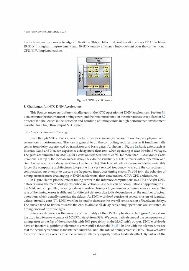
J. Low Power Electron. Appl. 2020, 10, 33
the architecture from server to edge applications. This architectural configuration allows TPU to achieve15–30 X throughput improvement and 30–80 X energy efficiency improvement over the conventionalCPU/GPU implementations.
Figure 1. TPU Systolic Array.
3. Challenges for NTC DNN Accelerators
This Section uncovers different challenges in the NTC operation of DNN accelerators. Section 3.1demonstrates the occurrence of timing errors and their manifestations on the inference accuracy. Section 3.2presents the challenges in the detection and handling of timing errors in high performance environmentessential for a high throughput NTC system.
3.1. Unique Performance Challenge
Even though NTC circuits give a quadratic decrease in energy consumption, they are plagued withsevere loss in performance. The loss is general to all the computing architectures as it fundamentallycomes from delay experienced by transistors and basic gates. As shown in Figure 2a, basic gates, such asInverter, Nand and Nor, can experience a delay more than 10×, when operating at near threshold voltages.The gates are simulated in HSPICE for a constant temperature of 25 ◦C, for more than 10,000 Monte-Carloiterations. On top of the increase in base delay, the extreme sensitivity of NTC circuits with temperature andcircuit noise results in a delay variation of up to 5× [14]. This level of delay increase and delay variabilityforces the computing architectures to operate in a very relaxed frequency, to ensure the correctness incomputation. An attempt to upscale the frequency introduces timing errors. To add to it, the behavior oftiming errors is more challenging in DNN accelerators, than conventional CPU/GPU architectures.
In Figure 2b, we plot the rate of timing errors in the inference computations in a TPU of eight DNNdatasets using the methodology described in Section 5. As there can be computations happening in allthe MAC units in parallel, crossing a delay threshold brings a huge number of timing errors at once. Therate of the timing errors is different for different datasets due to its dependence on the number of actualoperations which actually sensitize the delays. As DNN workload consists of several clusters of identicalvalues, (usually zero [2]), DNN workloads tend to decrease the overall sensitization of hardware delays.The curves tend to flatten towards the end as almost all delay sensitizing operations are saturated astiming errors at prior voltages.
Inference Accuracy is the measure of the quality of the DNN applications. In Figure 2c, we showthe drop in inference accuracy of MNIST dataset from 98%. We conservatively model the consequence oftiming error as the flip of the correct bit with 50% probability in the MAC unit’s output. DNN workloadshave an inherent algorithmic tolerance to error until a threshold [34,35]. In line with the tolerance, we seethat the accuracy variation is maintained under 5% until the rate of timing errors is 0.02%. However, afterthe error tolerance exceeds this, the accuracy falls very rapidly with a landslide effect. By virtue of the
66
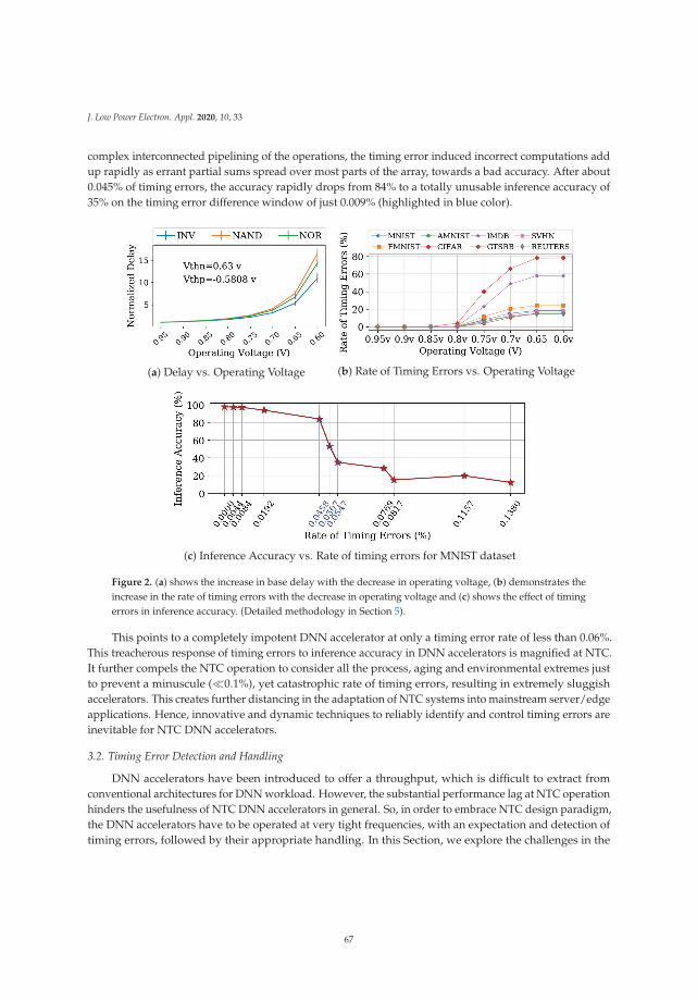
J. Low Power Electron. Appl. 2020, 10, 33
complex interconnected pipelining of the operations, the timing error induced incorrect computations addup rapidly as errant partial sums spread over most parts of the array, towards a bad accuracy. After about0.045% of timing errors, the accuracy rapidly drops from 84% to a totally unusable inference accuracy of35% on the timing error difference window of just 0.009% (highlighted in blue color).
(a) Delay vs. Operating Voltage (b) Rate of Timing Errors vs. Operating Voltage
(c) Inference Accuracy vs. Rate of timing errors for MNIST dataset
Figure 2. (a) shows the increase in base delay with the decrease in operating voltage, (b) demonstrates theincrease in the rate of timing errors with the decrease in operating voltage and (c) shows the effect of timingerrors in inference accuracy. (Detailed methodology in Section 5).
This points to a completely impotent DNN accelerator at only a timing error rate of less than 0.06%.This treacherous response of timing errors to inference accuracy in DNN accelerators is magnified at NTC.It further compels the NTC operation to consider all the process, aging and environmental extremes justto prevent a minuscule (�0.1%), yet catastrophic rate of timing errors, resulting in extremely sluggishaccelerators. This creates further distancing in the adaptation of NTC systems into mainstream server/edgeapplications. Hence, innovative and dynamic techniques to reliably identify and control timing errors areinevitable for NTC DNN accelerators.
3.2. Timing Error Detection and Handling
DNN accelerators have been introduced to offer a throughput, which is difficult to extract fromconventional architectures for DNN workload. However, the substantial performance lag at NTC operationhinders the usefulness of NTC DNN accelerators in general. So, in order to embrace NTC design paradigm,the DNN accelerators have to be operated at very tight frequencies, with an expectation and detection oftiming errors, followed by their appropriate handling. In this Section, we explore the challenges in the
67
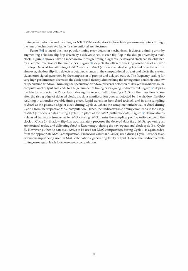
J. Low Power Electron. Appl. 2020, 10, 33
timing error detection and handling for NTC DNN accelerators in these high performance points throughthe lens of techniques available for conventional architectures.
Razor [36] is one of the most popular timing error detection mechanisms. It detects a timing error byaugmenting a shadow flip-flop driven by a delayed clock, to each flip-flop in the design driven by a mainclock. Figure 3 shows Razor’s mechanism through timing diagrams. A delayed clock can be obtainedby a simple inversion of the main clock. Figure 3a depicts the efficient working conditions of a Razorflip-flop. Delayed transitioning of data2 results in data1 (erroneous data) being latched onto the output.However, shadow flip-flop detects a detained change in the computational output and alerts the systemvia an error signal, generated by the comparison of prompt and delayed output. The frequency scaling forvery high performances decreases the clock period thereby, diminishing the timing error detection windowor speculation window. Shrinking the speculation window, prevents detection of delayed transitions in thecomputational output and leads to a huge number of timing errors going undiscovered. Figure 3b depictsthe late transition in the Razor Input during the second half of the Cycle 1. Since the transition occursafter the rising edge of delayed clock, the data manifestation goes undetected by the shadow flip-flopresulting in an undiscoverable timing error. Rapid transition from data2 to data3, and in-time samplingof data3 at the positive edge of clock during Cycle 2, ushers the complete withdrawal of data2 duringCycle 1 from the respective MAC computation. Hence, the undiscoverable timing error leads to the usageof data1 (erroneous data) during Cycle 1, in place of the data2 (authentic data). Figure 3c demonstratesa delayed transition from data2 to data3, causing data3 to miss the sampling point (positive edge of theclock in Cycle 2). Shadow flip-flop appropriately procures the delayed data (i.e., data3), spawning anarchitectural replay and delivering data3 to Razor output during the next operational clock cycle (i.e., Cycle3). However, authentic data (i.e., data2) to be used for MAC computation during Cycle 1, is again cededfrom the appropriate MAC’s computation. Erroneous values (i.e., data1) used during Cycle 1, render to anerroneous input being used in MAC calculations, generating faulty output. Hence, the undiscoverabletiming error again leads to an erroneous computation.
68
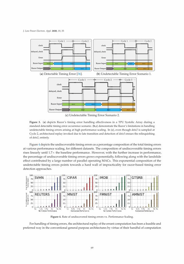
J. Low Power Electron. Appl. 2020, 10, 33
(a) Detectable Timing Error [36]. (b) Undetectable Timing Error Scenario 1.
(c) Undetectable Timing Error Scenario 2.
Figure 3. (a) depicts Razor’s timing error handling effectiveness in a TPU Systolic Array during astandard detectable timing error occurrence scenario. (b,c) demonstrate the Razor’s limitations in handlingundetectable timing errors arising at high performance scaling. In (c), even though data2 is sampled atCycle 2, architectural replay invoked due to late transition and detection of data3 ensues the relinquishingof data2, entirely.
Figure 4 depicts the undiscoverable timing errors as a percentage composition of the total timing errorsat various performance scaling, for different datasets. The composition of undiscoverable timing errorsrises linearly until 1.7× the baseline performance. However, with the further increase in performance,the percentage of undiscoverable timing errors grows exponentially, following along with the landslideeffect contributed by a large number of parallel operating MACs. This exponential composition of theundetectable timing errors points towards a hard wall of impracticality for razor-based timing errordetection approaches.
Figure 4. Rate of undiscovered timing errors vs. Performance Scaling.
For handling of timing errors, the architectural replay of the errant computation has been a feasible andpreferred way in the conventional general purpose architectures by virtue of their handful of computation
69
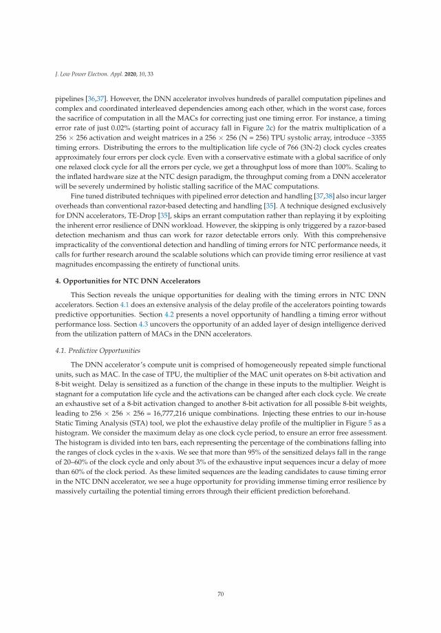
J. Low Power Electron. Appl. 2020, 10, 33
pipelines [36,37]. However, the DNN accelerator involves hundreds of parallel computation pipelines andcomplex and coordinated interleaved dependencies among each other, which in the worst case, forcesthe sacrifice of computation in all the MACs for correcting just one timing error. For instance, a timingerror rate of just 0.02% (starting point of accuracy fall in Figure 2c) for the matrix multiplication of a256 × 256 activation and weight matrices in a 256 × 256 (N = 256) TPU systolic array, introduce ~3355timing errors. Distributing the errors to the multiplication life cycle of 766 (3N-2) clock cycles createsapproximately four errors per clock cycle. Even with a conservative estimate with a global sacrifice of onlyone relaxed clock cycle for all the errors per cycle, we get a throughput loss of more than 100%. Scaling tothe inflated hardware size at the NTC design paradigm, the throughput coming from a DNN acceleratorwill be severely undermined by holistic stalling sacrifice of the MAC computations.
Fine tuned distributed techniques with pipelined error detection and handling [37,38] also incur largeroverheads than conventional razor-based detecting and handling [35]. A technique designed exclusivelyfor DNN accelerators, TE-Drop [35], skips an errant computation rather than replaying it by exploitingthe inherent error resilience of DNN workload. However, the skipping is only triggered by a razor-baseddetection mechanism and thus can work for razor detectable errors only. With this comprehensiveimpracticality of the conventional detection and handling of timing errors for NTC performance needs, itcalls for further research around the scalable solutions which can provide timing error resilience at vastmagnitudes encompassing the entirety of functional units.
4. Opportunities for NTC DNN Accelerators
This Section reveals the unique opportunities for dealing with the timing errors in NTC DNNaccelerators. Section 4.1 does an extensive analysis of the delay profile of the accelerators pointing towardspredictive opportunities. Section 4.2 presents a novel opportunity of handling a timing error withoutperformance loss. Section 4.3 uncovers the opportunity of an added layer of design intelligence derivedfrom the utilization pattern of MACs in the DNN accelerators.
4.1. Predictive Opportunities
The DNN accelerator’s compute unit is comprised of homogeneously repeated simple functionalunits, such as MAC. In the case of TPU, the multiplier of the MAC unit operates on 8-bit activation and8-bit weight. Delay is sensitized as a function of the change in these inputs to the multiplier. Weight isstagnant for a computation life cycle and the activations can be changed after each clock cycle. We createan exhaustive set of a 8-bit activation changed to another 8-bit activation for all possible 8-bit weights,leading to 256 × 256 × 256 = 16,777,216 unique combinations. Injecting these entries to our in-houseStatic Timing Analysis (STA) tool, we plot the exhaustive delay profile of the multiplier in Figure 5 as ahistogram. We consider the maximum delay as one clock cycle period, to ensure an error free assessment.The histogram is divided into ten bars, each representing the percentage of the combinations falling intothe ranges of clock cycles in the x-axis. We see that more than 95% of the sensitized delays fall in the rangeof 20–60% of the clock cycle and only about 3% of the exhaustive input sequences incur a delay of morethan 60% of the clock period. As these limited sequences are the leading candidates to cause timing errorin the NTC DNN accelerator, we see a huge opportunity for providing immense timing error resilience bymassively curtailing the potential timing errors through their efficient prediction beforehand.
70
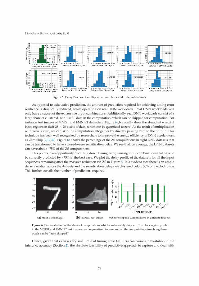
J. Low Power Electron. Appl. 2020, 10, 33
Figure 5. Delay Profiles of multiplier, accumulator and different datasets.
As opposed to exhaustive prediction, the amount of prediction required for achieving timing errorresilience is drastically reduced, while operating on real DNN workloads. Real DNN workloads willonly have a subset of the exhaustive input combinations. Additionally, real DNN workloads consist of alarge share of clustered, non-useful data in the computation, which can be skipped for computation. Forinstance, test images of MNIST and FMNIST datasets in Figure 6a,b visually show the abundant wastefulblack regions in their 28 × 28 pixels of data, which can be quantized to zero. As the result of multiplicationwith zero is zero, we can skip the computation altogether by directly passing zero to the output. Thistechnique has been well recognized by researchers to improve the energy efficiency of DNN accelerators,as Zero-Skip [2,19,39]. Figure 6c shows the percentage of the ZS computations in eight DNN datasets thatcan be transformed to have a close-to-zero sensitization delay. We see that, on average, the DNN datasetscan have about ~75% of the ZS computations.
This points to an opportunity of cutting down timing error, causing input combinations that have tobe correctly predicted by ~75% in the best case. We plot the delay profile of the datasets for all the inputsequences remaining after the massive reduction via ZS in Figure 5. It is evident that there is an ampledelay variation across the datasets and the sensitization delays are clustered below 50% of the clock cycle.This further curtails the number of predictions required.
(a) MNIST test image. (b) FMNIST test image. (c) Zero Skipable Computations in different datasets.
Figure 6. Demonstration of the share of computations which can be safely skipped. The black region pixelsin the MNIST and FMNIST test images can be quantized to zero and all the computations involving thosepixels can be “zero skipped”.
Hence, given that even a very small rate of timing error (�0.1%) can cause a devastation in theinference accuracy (Section 2), the absolute feasibility of predictive approach to capture and deal with
71
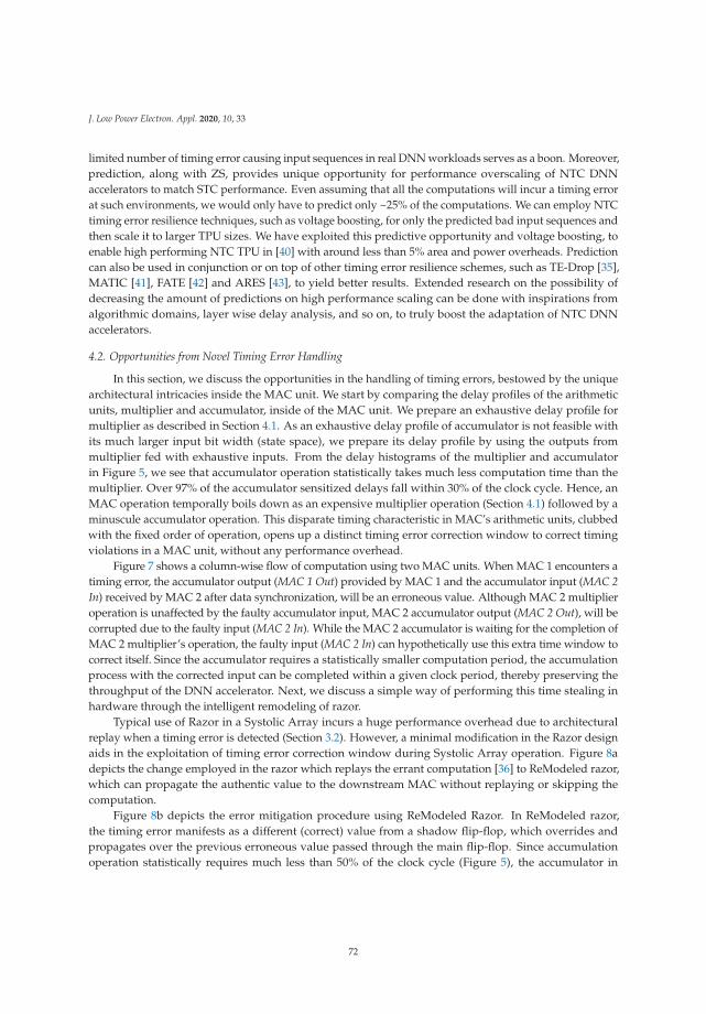
J. Low Power Electron. Appl. 2020, 10, 33
limited number of timing error causing input sequences in real DNN workloads serves as a boon. Moreover,prediction, along with ZS, provides unique opportunity for performance overscaling of NTC DNNaccelerators to match STC performance. Even assuming that all the computations will incur a timing errorat such environments, we would only have to predict only ~25% of the computations. We can employ NTCtiming error resilience techniques, such as voltage boosting, for only the predicted bad input sequences andthen scale it to larger TPU sizes. We have exploited this predictive opportunity and voltage boosting, toenable high performing NTC TPU in [40] with around less than 5% area and power overheads. Predictioncan also be used in conjunction or on top of other timing error resilience schemes, such as TE-Drop [35],MATIC [41], FATE [42] and ARES [43], to yield better results. Extended research on the possibility ofdecreasing the amount of predictions on high performance scaling can be done with inspirations fromalgorithmic domains, layer wise delay analysis, and so on, to truly boost the adaptation of NTC DNNaccelerators.
4.2. Opportunities from Novel Timing Error Handling
In this section, we discuss the opportunities in the handling of timing errors, bestowed by the uniquearchitectural intricacies inside the MAC unit. We start by comparing the delay profiles of the arithmeticunits, multiplier and accumulator, inside of the MAC unit. We prepare an exhaustive delay profile formultiplier as described in Section 4.1. As an exhaustive delay profile of accumulator is not feasible withits much larger input bit width (state space), we prepare its delay profile by using the outputs frommultiplier fed with exhaustive inputs. From the delay histograms of the multiplier and accumulatorin Figure 5, we see that accumulator operation statistically takes much less computation time than themultiplier. Over 97% of the accumulator sensitized delays fall within 30% of the clock cycle. Hence, anMAC operation temporally boils down as an expensive multiplier operation (Section 4.1) followed by aminuscule accumulator operation. This disparate timing characteristic in MAC’s arithmetic units, clubbedwith the fixed order of operation, opens up a distinct timing error correction window to correct timingviolations in a MAC unit, without any performance overhead.
Figure 7 shows a column-wise flow of computation using two MAC units. When MAC 1 encounters atiming error, the accumulator output (MAC 1 Out) provided by MAC 1 and the accumulator input (MAC 2In) received by MAC 2 after data synchronization, will be an erroneous value. Although MAC 2 multiplieroperation is unaffected by the faulty accumulator input, MAC 2 accumulator output (MAC 2 Out), will becorrupted due to the faulty input (MAC 2 In). While the MAC 2 accumulator is waiting for the completion ofMAC 2 multiplier’s operation, the faulty input (MAC 2 In) can hypothetically use this extra time window tocorrect itself. Since the accumulator requires a statistically smaller computation period, the accumulationprocess with the corrected input can be completed within a given clock period, thereby preserving thethroughput of the DNN accelerator. Next, we discuss a simple way of performing this time stealing inhardware through the intelligent remodeling of razor.
Typical use of Razor in a Systolic Array incurs a huge performance overhead due to architecturalreplay when a timing error is detected (Section 3.2). However, a minimal modification in the Razor designaids in the exploitation of timing error correction window during Systolic Array operation. Figure 8adepicts the change employed in the razor which replays the errant computation [36] to ReModeled razor,which can propagate the authentic value to the downstream MAC without replaying or skipping thecomputation.
Figure 8b depicts the error mitigation procedure using ReModeled Razor. In ReModeled razor,the timing error manifests as a different (correct) value from a shadow flip-flop, which overrides andpropagates over the previous erroneous value passed through the main flip-flop. Since accumulationoperation statistically requires much less than 50% of the clock cycle (Figure 5), the accumulator in
72
J. Low Power Electron. Appl. 2020, 10, 33
the downstream MAC can quickly recompute with the correct value. The presence of ZS computations(Figure 6c) further aids the timing error correction window, as the skippable multiplier operations leave theaccumulator to sensitize only to the upstream MAC’s output. Figure 9 demonstrates the RTL simulationsfor Razor/Remodeled Razor in the absence and presence of a timing error. Figure 9a depicts the standardwaveform for a timing error free operation. Figure 9b shows an occurrence of a timing error due to aminor delay in the Razor input and the stretching of operational cycle to procure the correct value for there-computation process. Figure 9c elaborates the detection and correction of the timing error, within thesame clock cycle. Although, Razor adds buffers on short paths to avoid hold time violations, Zhang etal. [44] have modeled the additional buffers in timing simulations and determined that in a MAC unitonly 14 out of 40 flip-flops requires a protection by Razor, which only adds a power penalty of 3.34%. Theaddition of ReModeled Razor into the Systolic Array adds an area overhead of only 5% into the TPU. Inlight of these findings, it is evident that we can extract novel opportunities to handle the timing errors atNTC by additional research on fine-tuning the combinational delays among the various arithmetic blocksinside the DNN accelerator. We have exploited this opportunistic timing error mitigation strategy in [45]to provide timing error resilience in a DNN systolic array.
Figure 7. Column-Wise MAC Operation.
73
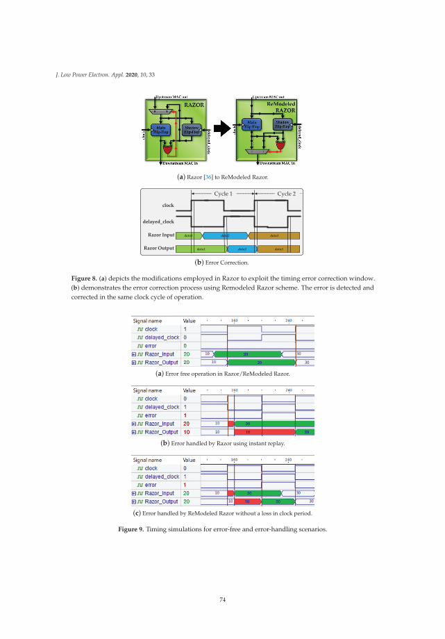
J. Low Power Electron. Appl. 2020, 10, 33
(a) Razor [36] to ReModeled Razor.
(b) Error Correction.
Figure 8. (a) depicts the modifications employed in Razor to exploit the timing error correction window.(b) demonstrates the error correction process using Remodeled Razor scheme. The error is detected andcorrected in the same clock cycle of operation.
(a) Error free operation in Razor/ReModeled Razor.
(b) Error handled by Razor using instant replay.
(c) Error handled by ReModeled Razor without a loss in clock period.
Figure 9. Timing simulations for error-free and error-handling scenarios.
74
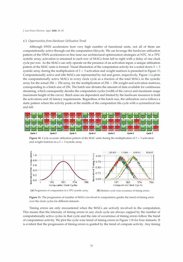
J. Low Power Electron. Appl. 2020, 10, 33
4.3. Opportunities from Hardware Utilization Trend
Although DNN accelerators host very high number of functional units, not all of them arecomputationally active through out the computation lifecycle. We can leverage the hardware utilizationpattern of the DNN accelerators to fine tune our architectural optimization strategies at NTC. In a TPUsystolic array, activation is streamed to each row of MACs from left to right with a delay of one clockcycle per row. As the MACs can only operate on the presence of an activation input, a unique utilizationpattern of the MAC units is formed. Visual illustration of the computation activity for a scaled down 3 × 3systolic array during the multiplication of 3 × 3 activation and weight matrices is presented in Figure 10.Computationally active and idle MACs are represented by red and green, respectively. Figure 11a plotsthe computationally active MACs in every clock cycle as a fraction of the total MACs in the systolicarray for the actual 256 × 256 array, for the multiplication of 256 × 256 weight and activation matrices,corresponding to a batch size of 256. The batch size dictates the amount of data available for continuousstreaming, which consequently decides the computation cycles (width of the curve) and maximum usage(maximum height of the curve). Batch sizes are dependent and limited by the hardware resources to holdthe activations and AI latency requirements. Regardless of the batch size, the utilization curve follows astatic pattern where the activity peaks at the middle of the computation life cycle with a symmetrical riseand fall.
Figure 10. Cycle accurate utilization pattern of the MAC units during the multiplication of 3 × 3 activationand weight matrices in a 3 × 3 systolic array.
(a) Progression of computation in a TPU systolic array. (b) Relative cycle wise occurence of timing errors.
Figure 11. The progression of number of MACs involved in computation guides the trend of timing errorover the clock cycles for different datasets.
Timing errors are only encountered when the MACs are actively involved in the computation.This means that the intensity of timing errors in any clock cycle are always capped by the number ofcomputationally active cycles in that cycle and the rate of occurrence of timing errors follow the trendof computation activity. We plot the cycle wise trend of timing errors in Figure 11b for four datasets. Itis evident that the progression of timing errors is guided by the trend of compute activity. Any timing
75
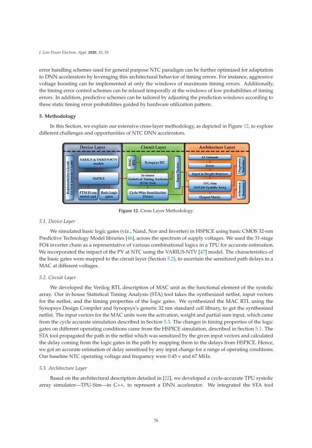
J. Low Power Electron. Appl. 2020, 10, 33
error handling schemes used for general purpose NTC paradigm can be further optimized for adaptationto DNN accelerators by leveraging this architectural behavior of timing errors. For instance, aggressivevoltage boosting can be implemented at only the windows of maximum timing errors. Additionally,the timing error control schemes can be relaxed temporally at the windows of low probabilities of timingerrors. In addition, predictive schemes can be tailored by adjusting the prediction windows according tothese static timing error probabilities guided by hardware utilization pattern.
5. Methodology
In this Section, we explain our extensive cross-layer methodology, as depicted in Figure 12, to exploredifferent challenges and opportunities of NTC DNN accelerators.
Figure 12. Cross Layer Methodology.
5.1. Device Layer
We simulated basic logic gates (viz., Nand, Nor and Inverter) in HSPICE using basic CMOS 32-nmPredictive Technology Model libraries [46], across the spectrum of supply voltages. We used the 31-stageFO4 inverter chain as a representative of various combinational logics in a TPU for accurate estimation.We incorporated the impact of the PV at NTC using the VARIUS-NTV [47] model. The characteristics ofthe basic gates were mapped to the circuit layer (Section 5.2), to ascertain the sensitized path delays in aMAC at different voltages.
5.2. Circuit Layer
We developed the Verilog RTL description of MAC unit as the functional element of the systolicarray. Our in-house Statistical Timing Analysis (STA) tool takes the synthesized netlist, input vectorsfor the netlist, and the timing properties of the logic gates. We synthesized the MAC RTL using theSynopsys Design Compiler and Synopsys’s generic 32 nm standard cell library, to get the synthesizednetlist. The input vectors for the MAC units were the activation, weight and partial sum input, which camefrom the cycle accurate simulation described in Section 5.3. The changes in timing properties of the logicgates on different operating conditions came from the HSPICE simulation, described in Section 5.1. TheSTA tool propagated the path in the netlist which was sensitized by the given input vectors and calculatedthe delay coming from the logic gates in the path by mapping them to the delays from HSPICE. Hence,we got an accurate estimation of delay sensitized by any input change for a range of operating conditions.Our baseline NTC operating voltage and frequency were 0.45 v and 67 MHz.
5.3. Architecture Layer
Based on the architectural description detailed in [22], we developed a cycle-accurate TPU systolicarray simulator—TPU-Sim—in C++, to represent a DNN accelerator. We integrated the STA tool
76
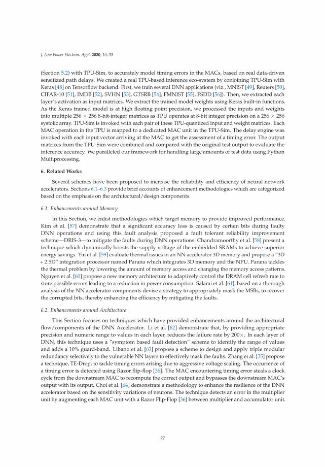
J. Low Power Electron. Appl. 2020, 10, 33
(Section 5.2) with TPU-Sim, to accurately model timing errors in the MACs, based on real data-drivensensitized path delays. We created a real TPU-based inference eco-system by conjoining TPU-Sim withKeras [48] on Tensorflow backend. First, we train several DNN applications (viz., MNIST [49], Reuters [50],CIFAR-10 [51], IMDB [52], SVHN [53], GTSRB [54], FMNIST [55], FSDD [56]). Then, we extracted eachlayer’s activation as input matrices. We extract the trained model weights using Keras built-in functions.As the Keras trained model is at high floating point precision, we processed the inputs and weightsinto multiple 256 × 256 8-bit-integer matrices as TPU operates at 8-bit integer precision on a 256 × 256systolic array. TPU-Sim is invoked with each pair of these TPU-quantized input and weight matrices. EachMAC operation in the TPU is mapped to a dedicated MAC unit in the TPU-Sim. The delay engine wasinvoked with each input vector arriving at the MAC to get the assessment of a timing error. The outputmatrices from the TPU-Sim were combined and compared with the original test output to evaluate theinference accuracy. We paralleled our framework for handling large amounts of test data using PythonMultiprocessing.
6. Related Works
Several schemes have been proposed to increase the reliability and efficiency of neural networkaccelerators. Sections 6.1–6.3 provide brief accounts of enhancement methodologies which are categorizedbased on the emphasis on the architectural/design components.
6.1. Enhancements around Memory
In this Section, we enlist methodologies which target memory to provide improved performance.Kim et al. [57] demonstrate that a significant accuracy loss is caused by certain bits during faultyDNN operations and using this fault analysis proposed a fault tolerant reliability improvementscheme—DRIS-3—to mitigate the faults during DNN operations. Chandramoorthy et al. [58] present atechnique which dynamically boosts the supply voltage of the embedded SRAMs to achieve superiorenergy savings. Yin et al. [59] evaluate thermal issues in an NN accelerator 3D memory and propose a “3D+ 2.5D” integration processor named Parana which integrates 3D memory and the NPU. Parana tacklesthe thermal problem by lowering the amount of memory access and changing the memory access patterns.Nguyen et al. [60] propose a new memory architecture to adaptively control the DRAM cell refresh rate tostore possible errors leading to a reduction in power consumption. Salami et al. [61], based on a thoroughanalysis of the NN accelerator components devise a strategy to appropriately mask the MSBs, to recoverthe corrupted bits, thereby enhancing the efficiency by mitigating the faults.
6.2. Enhancements around Architecture
This Section focuses on techniques which have provided enhancements around the architecturalflow/components of the DNN Accelerator. Li et al. [62] demonstrate that, by providing appropriateprecision and numeric range to values in each layer, reduces the failure rate by 200×. In each layer ofDNN, this technique uses a ”symptom based fault detection” scheme to identify the range of valuesand adds a 10% guard-band. Libano et al. [63] propose a scheme to design and apply triple modularredundancy selectively to the vulnerable NN layers to effectively mask the faults. Zhang et al. [35] proposea technique, TE-Drop, to tackle timing errors arising due to aggressive voltage scaling. The occurrence ofa timing error is detected using Razor flip-flop [36]. The MAC encountering timing error steals a clockcycle from the downstream MAC to recompute the correct output and bypasses the downstream MAC’soutput with its output. Choi et al. [64] demonstrate a methodology to enhance the resilience of the DNNaccelerator based on the sensitivity variations of neurons. The technique detects an error in the multiplierunit by augmenting each MAC unit with a Razor Flip-Flop [36] between multiplier and accumulator unit.
77
J. Low Power Electron. Appl. 2020, 10, 33
Occurrence of a timing error will be lead to the upstream partial sum to be bypassed on to the downstreamMAC unit. Zhang et al. [65] address the reliability concerns due to permanent faults arising from MACunits by mapping and pruning the weights of faulty MAC units.
6.3. Enhancements around Analog/Mixed-Signal Domain
Analog and mixed-signal DNN accelerators are also making a mark in the Neural Networkcomputing realm. Analog and mixed-signal accelerators use enhanced Analog-to-Digital converter(ADC), Digital-to-Analog converter (DAC) for encoding/decoding and Non-Volatile Memories, such asReRAM’s in DNN-based computations. Eshraghian et al. [66] utilize the frequency dependence of v-i placehysteresis to relieve the limitation on the single-bit-per-device and allocating the kernel information to thedevice conductance and partially to the frequency of the time-varying input. Ghodrati et al. [67] propose atechnique BIHIWE, to address the issues in mixed-signal circuitry due to restricted scope of informationencoding, noise susceptibility and overheads due to Analog to Digital conversions. BIHIWE, bit-partitionsvector dot-product into clusters of low-bitwidth operations executing in parallel and embedding acrossmultiple vector elements. Shafiee et al. [26] demonstrate a scheme ISAAC, by implementing a pipelinedarchitecture with each neural network layer being dedicated specific crossbars and heaping up the databetween pipe stages using eDRAM buffers. ISAAC also proposes a novel data encoding technique toreduce the analog-to-digital conversion overheads and performs a design space inspection to obtaina balance between memristor storage/compute, buffers and ADCs on the chip. Mackin et al. [68]propose the usage of crossbar arrays of NVMs to implement MAC operations at the data location anddemonstrates simultaneous programming of weights at optimal hardware conditions and exploring itseffectiveness under significant NVM variability. These recent developments in Analog and Mixed-signalDNN accelerators envision employing ADC, DAC and ReRAM’s in NTC DNN accelerators to yield betterenergy efficiency. Successive Approximation Register ADCs can be efficiently utilized at NTC owing totheir simple architecture and low power usage [69–73]. In addition, the efficacy of ReRAM [74–79] in alow power computing environment provides a promising direction in DNN accelerators venturing intothe NTC realm.
7. Conclusions
The NTC design paradigm, being a stronger direction towards energy efficiency, is plagued by timingerrors for DNN applications. In this paper, we illustrate the unique challenges coming from the DNNworkload and attributes of the occurrence and impact of timing errors. We discover that NTC DNNaccelerators are challenged by landslide increases in the rate timing errors and the inherent algorithmictolerance of DNNs to timing errors is quickly surpassed with a sharp decline in the inference accuracy.We explore the data–delay relationship with the practical DNN datasets to uncover an opportunity ofproviding bulk timing error resilience through prediction of a small group of high delay input sequences.We explore the timing disparities in the multiplier and accumulator to propose opportunities for providingan elegant timing error correction without performance loss. We correlate the hardware utilization patternto outshine the broad control strategies for timing error resilience techniques. The application of NTC inthe domain of DNN accelerators is a relatively newer domain and this article serves to present concretepossible directions towards timing error resilience, which remains to be a big hurdle for NTC systems.Energy efficient AI evolution is the need of the hour and further research with promising domains, such asNTC is required.
Author Contributions: Conceptualization, P.P. and N.D.G.; methodology, P.P., N.D.G., P.B. and T.S.; software, P.B., P.P.,N.D.G. and T.S.; validation, P.P. and N.D.G.; formal analysis, P.P. and N.D.G.; investigation, P.P., N.D.G., P.B., T.S. andM.C.P.; resources, P.P., N.D.G., P.B., T.S., K.C. and S.R.; data curation, P.P.; writing—original draft preparation, P.P. and
78
J. Low Power Electron. Appl. 2020, 10, 33
N.D.G.; writing—review and editing, P.P., N.D.G., K.C. and S.R.; visualization, P.P. and N.D.G.; supervision, K.C. andS.R.; project administration, P.P.; funding acquisition, K.C. and S.R. All authors have read and agreed to the publishedversion of the manuscript.
Funding: This research was supported in part by National Science Foundation under grant numbers CAREER-1253024and CNS-1421022.
Conflicts of Interest: The authors declare no conflict of interest.
References
1. AI Will Add 15 Trillion to the World Economy by 2030. Available online: https://www.forbes.com/sites/greatspeculations/2019/02/25/ai-will-add-15-trillion-to-the-world-economy-by-2030/ (accessed on20 September 2020).
2. Reagen, B.; Whatmough, P.; Adolf, R.; Rama, S.; Lee, H.; Lee, S.K.; Hernández-Lobato, J.M.; Wei, G.Y.; Brooks, D.Minerva: Enabling low-power, highly-accurate deep neural network accelerators. In ACM SIGARCH ComputerArchitecture News; IEEE Press: Piscataway, NJ, USA, 2016; Volume 44, pp. 267–278.
3. Chen, Y.H.; Emer, J.; Sze, V. Using dataflow to optimize energy efficiency of deep neural network accelerators.IEEE Micro 2017, 37, 12–21. [CrossRef]
4. Kim, S.; Howe, P.; Moreau, T.; Alaghi, A.; Ceze, L.; Sathe, V.S. Energy-Efficient Neural Network Acceleration inthe Presence of Bit-Level Memory Errors. IEEE Trans. Circuits Syst. I Regul. Pap. 2018, 65, 4285–4298. [CrossRef]
5. Gokhale, V.; Zaidy, A.; Chang, A.X.M.; Culurciello, E. Snowflake: An efficient hardware accelerator forconvolutional neural networks. In Proceedings of the 2017 IEEE International Symposium on Circuits andSystems (ISCAS), Baltimore, MD, USA, 28–31 May 2017; pp. 1–4.
6. Sze, V.; Chen, Y.H.; Yang, T.J.; Emer, J.S. Efficient processing of deep neural networks: A tutorial and survey.Proc. IEEE 2017, 105, 2295–2329. [CrossRef]
7. Andrae, A.S.; Edler, T. On global electricity usage of communication technology: Trends to 2030. Challenges 2015,6, 117–157. [CrossRef]
8. Seok, M.; Jeon, D.; Chakrabarti, C.; Blaauw, D.; Sylvester, D. Pipeline Strategy for Improving Optimal EnergyEfficiency in Ultra-Low Voltage Design. In Proceedings of the 48th Design Automation Conference, San Diego,CA, USA, 5–10 June 2011; pp. 990–995.
9. Chen, H.; Manzi, D.; Roy, S.; Chakraborty, K. Opportunistic turbo execution in NTC: Exploiting the paradigmshift in performance bottlenecks. In Proceedings of the 2015 52nd ACM/EDAC/IEEE Design AutomationConference (DAC), San Francisco, CA, USA, 8–12 June 2015; pp. 63:1–63:6.
10. Mugisha, D.M.; Chen, H.; Roy, S.; Chakraborty, K. Resilient Cache Design for Mobile Processors in theNear-Threshold Regime. J. Low Power Electron. 2015, 11, 112–120. [CrossRef]
11. Basu, P.; Chen, H.; Saha, S.; Chakraborty, K.; Roy, S. SwiftGPU: Fostering Energy Efficiency in a Near-ThresholdGPU Through a Tactical Performance Boost. In Proceedings of the 2016 53nd ACM/EDAC/IEEE DesignAutomation Conference (DAC), Austin, TX, USA, 5–9 June 2016.
12. Pinckney, N.; Blaauw, D.; Sylvester, D. Low-power near-threshold design: Techniques to improve energyefficiency energy-efficient near-threshold design has been proposed to increase energy efficiency across a wid.IEEE Solid State Circuits Mag. 2015, 7, 49–57. [CrossRef]
13. Pinckney, N.R.; Sewell, K.; Dreslinski, R.G.; Fick, D.; Mudge, T.N.; Sylvester, D.; Blaauw, D. Assessing theperformance limits of parallelized near-threshold computing. In Proceedings of the 49th Annual DesignAutomation Conference, San Francisco, CA, USA, 3–7 June 2012; pp. 1147–1152.
14. Dreslinski, R.G.; Wieckowski, M.; Blaauw, D.; Sylvester, D.; Mudge, T.N. Near-Threshold Computing: ReclaimingMoore’s Law Through Energy Efficient Integrated Circuits. Proc. IEEE 2010, 98, 253–266. [CrossRef]
15. Shabanian, T.; Bal, A.; Basu, P.; Chakraborty, K.; Roy, S. ACE-GPU: Tackling Choke Point Induced PerformanceBottlenecks in a Near-Threshold Computing GPU. In Proceedings of the International Symposium on LowPower Electronics and Design (ISLPED ’18), Bellevue, WA, USA, 23–25 July 2018.
79
J. Low Power Electron. Appl. 2020, 10, 33
16. Trapani Possignolo, R.; Ebrahimi, E.; Ardestani, E.K.; Sankaranarayanan, A.; Briz, J.L.; Renau, J. GPU NTC ProcessVariation Compensation With Voltage Stacking. IEEE Trans. Very Large Scale Integr. Syst. 2018, 26, 1713–1726.[CrossRef]
17. Esmaeilzadeh, H.; Blem, E.; Amant, R.S.; Sankaralingam, K.; Burger, D. Dark silicon and the end of multicorescaling. In Proceedings of the 2011 38th Annual International Symposium on Computer Architecture (ISCA),San Jose, CA, USA, 4–8 June 2011.
18. Silvano, C.; Palermo, G.; Xydis, S.; Stamelakos, I.S. Voltage island management in near threshold manycorearchitectures to mitigate dark silicon. In Proceedings of the 2014 Design, Automation & Test in Europe Conference& Exhibition (DATE), Dresden, Germany, 24–28 March 2014; pp. 1–6.
19. Chen, Y.H.; Krishna, T.; Emer, J.S.; Sze, V. Eyeriss: An energy-efficient reconfigurable accelerator for deepconvolutional neural networks. IEEE J. Solid State Circuits 2016, 52, 127–138. [CrossRef]
20. Yoo, H.J.; Park, S.; Bong, K.; Shin, D.; Lee, J.; Choi, S. A 1.93 tops/w scalable deep learning/inference processorwith tetra-parallel mimd architecture for big data applications. In Proceedings of the IEEE InternationalSolid-State Circuits Conference, San Francisco, CA, USA, 22–26 February 2015; pp. 80–81.
21. Cavigelli, L.; Gschwend, D.; Mayer, C.; Willi, S.; Muheim, B.; Benini, L. Origami: A convolutional networkaccelerator. In Proceedings of the 25th Edition on Great Lakes Symposium on VLSI, Pittsburgh, PA, USA, 20–22May 2015; pp. 199–204.
22. Jouppi, N.P.; Young, C.; Patil, N.; Patterson, D.; Agrawal, G.; Bajwa, R.; Bates, S.; Bhatia, S.; Boden, N.; Borchers,A.; et al. In-datacenter performance analysis of a tensor processing unit. In Proceedings of the 2017 ACM/IEEE44th Annual International Symposium on Computer Architecture (ISCA), Toronto, ON, Canada, 24–28 June 2017;pp. 1–12.
23. Du, Z.; Fasthuber, R.; Chen, T.; Ienne, P.; Li, L.; Luo, T.; Feng, X.; Chen, Y.; Temam, O. ShiDianNao: Shifting visionprocessing closer to the sensor. In Proceedings of the 2015 ACM/IEEE 42nd Annual International Symposiumon Computer Architecture (ISCA), Portland, OR, USA, 13–17 June 2015; pp. 92–104. [CrossRef]
24. Chen, T.; Du, Z.; Sun, N.; Wang, J.; Wu, C.; Chen, Y.; Temam, O. Diannao: A small-footprint high-throughputaccelerator for ubiquitous machine-learning. ACM Sigarch Comput. Archit. News 2014, 42, 269–284. [CrossRef]
25. Zhang, J.; Wang, Z.; Verma, N. A machine-learning classifier implemented in a standard 6T SRAMarray. In Proceedings of the 2016 IEEE Symposium on VLSI Circuits (VLSI-Circuits), Honolulu, HI, USA,15–17 June 2016; pp. 1–2.
26. Shafiee, A.; Nag, A.; Muralimanohar, N.; Balasubramonian, R.; Strachan, J.P.; Hu, M.; Williams, R.S.; Srikumar, V.ISAAC: A convolutional neural network accelerator with in-situ analog arithmetic in crossbars. ACM SigarchComput. Archit. News 2016, 44, 14–26. [CrossRef]
27. Chi, P.; Li, S.; Xu, C.; Zhang, T.; Zhao, J.; Liu, Y.; Wang, Y.; Xie, Y. Prime: A novel processing-in-memoryarchitecture for neural network computation in reram-based main memory. In Proceedings of the 43rdInternational Symposium on Computer Architecture, Seoul, Korea, 18–22 June 2016.
28. Song, L.; Qian, X.; Li, H.; Chen, Y. Pipelayer: A pipelined reram-based accelerator for deep learning.In Proceedings of the 2017 IEEE International Symposium on High Performance Computer Architecture (HPCA),Austin, TX, USA, 4–8 February 2017; pp. 541–552.
29. Mythic Technology: An Architecture Built from the Ground up for AI. Available online: https://www.mythic-ai.com/technology/ (accessed on 20 September 2020).
30. Graphcore IPU: Designed for Machine Intelligence. Available online: https://www.graphcore.ai/products/ipu(accessed on 20 September 2020).
31. Perceive Ergo: A Complete Solution for High Accuracy, Low Power Intelligence to Consumer Products. Availableonline: https://perceive.io/product/ (accessed on 20 September 2020).
32. Edge TPU: Google’s Purpose-Built ASIC Designed to Run Inference at the Edge. Available online: https://cloud.google.com/edge-tpu (accessed on 20 September 2020).
33. Google Coral Edge TPU Explained in Depth. Available online: https://qengineering.eu/google-corals-tpu-explained.html (accessed on 20 September 2020).
80
J. Low Power Electron. Appl. 2020, 10, 33
34. Jiao, X.; Luo, M.; Lin, J.H.; Gupta, R.K. An assessment of vulnerability of hardware neural networks to dynamicvoltage and temperature variations. In Proceedings of the 36th International Conference on Computer-AidedDesign, Irvine, CA, USA, 13–16 November 2017; pp. 945–950.
35. Zhang, J.; Rangineni, K.; Ghodsi, Z.; Garg, S. ThUnderVolt: Enabling Aggressive Voltage Underscaling and TimingError Resilience for Energy Efficient Deep Neural Network Accelerators. arXiv 2018, arXiv:1802.03806.
36. Ernst, D.; Kim, N.S.; Das, S.; Pant, S.; Rao, R.R.; Pham, T.; Ziesler, C.H.; Blaauw, D.; Austin, T.M.; Flautner, K.; et al.Razor: A Low-Power Pipeline Based on Circuit-Level Timing Speculation. In Proceedings of the 36th AnnualIEEE/ACM International Symposium on Microarchitecture (MICRO-36), San Diego, CA, USA, 5 December 2003;pp. 7–18.
37. Das, S.; Tokunaga, C.; Pant, S.; Ma, W.H.; Kalaiselvan, S.; Lai, K.; Bull, D.; Blaauw, D. RazorII: In Situ ErrorDetection and Correction for PVT and SER Tolerance. J. Solid State Circ. 2009, 44, 32–48. [CrossRef]
38. Fojtik, M.; Fick, D.; Kim, Y.; Pinckney, N.; Harris, D.; Blaauw, D.; Sylvester, D. Bubble Razor:An architecture-independent approach to timing-error detection and correction. In Proceedings of the 2012 IEEEInternational Solid-State Circuits Conference, San Francisco, California, USA, 19–23 February 2012; pp. 488–490.
39. Albericio, J.; Judd, P.; Hetherington, T.; Aamodt, T.; Jerger, N.E.; Moshovos, A. Cnvlutin: Ineffectual -Neuron-FreeDeep Neural Network Computing. In Proceedings of the 2016 ACM/IEEE 43rd Annual International Symposiumon Computer Architecture (ISCA), Seoul, Korea, 18–22 June 2016; pp. 1–13. [CrossRef]
40. Pandey, P.; Basu, P.; Chakraborty, K.; Roy, S. GreenTPU: Improving Timing Error Resilience of a Near-ThresholdTensor Processing Unit. In Proceedings of the 2019 56th ACM/IEEE Design Automation Conference (DAC), LasVegas, NV, USA, 2–6 June 2019; pp. 173:1–173:6.
41. Kim, S.; Howe, P.; Moreau, T.; Alaghi, A.; Ceze, L.; Sathe, V. MATIC: Learning around errors for efficientlow-voltage neural network accelerators. In Proceedings of the 2018 Design, Automation & Test in EuropeConference & Exhibition (DATE), Dresden, Germany, 19–23 March 2018; pp. 1–6.
42. Zhang, J.J.; Garg, S. FATE: fast and accurate timing error prediction framework for low power DNN acceleratordesign. In Proceedings of the 2018 IEEE/ACM International Conference on Computer-Aided Design (ICCAD);San Diego, CA, USA, 5–8 November 2018; pp. 1–8.
43. Reagen, B.; Gupta, U.; Pentecost, L.; Whatmough, P.; Lee, S.K.; Mulholland, N.; Brooks, D.; Wei, G.Y. Ares:A framework for quantifying the resilience of deep neural networks. In Proceedings of the 2018 55thACM/ESDA/IEEE Design Automation Conference (DAC), San Francisco, CA, USA, 24–28 June 2018; pp. 1–6.
44. Zhang, J.; Ghodsi, Z.; Rangineni, K.; Garg, S. Enabling Timing Error Resilience for Low-Power Systolic-ArrayBased Deep Learning Accelerators. IEEE Des. Test 2019, 37, 93–102. [CrossRef]
45. Gundi, N.D.; Shabanian, T.; Basu, P.; Pandey, P.; Roy, S.; Chakraborty, K.; Zhang, Z. EFFORT: Enhancing EnergyEfficiency and Error Resilience of a Near-Threshold Tensor Processing Unit. In Proceedings of the 2020 25th Asiaand South Pacific Design Automation Conference (ASP-DAC), Beijing, China, 13–16 January 2020; pp. 241–246.
46. Zhao, W.; Cao, Y. New Generation of Predictive Technology Model for sub-45nm Early Design Exploration.Electron. Devices 2006, 53, 2816–2823. [CrossRef]
47. Karpuzcu, U.R.; Kolluru, K.B.; Kim, N.S.; Torrellas, J. VARIUS-NTV: A microarchitectural model to capturethe increased sensitivity of manycores to process variations at near-threshold voltages. In Proceedings of theIEEE/IFIP International Conference on Dependable Systems and Networks (DSN 2012), Boston, MA, USA, 25–28June 2012; pp. 1–11.
48. Keras. Available online: https://keras.io (accessed on 20 September 2020).49. LeCun, Y.; Cortes, C. MNIST Handwritten Digit Database. Available online: http://yann.lecun.com/exdb/
mnist/ (accessed on 20 September 2020).50. Reuters-21578 Dataset. Available online: http://kdd.ics.uci.edu/databases/reuters21578/reuters21578.html
(accessed on 20 September 2020).51. Krizhevsky, A. Learning Multiple Layers of Features from Tiny Images. Available online: http://citeseerx.ist.
psu.edu/viewdoc/download?doi=10.1.1.222.9220&rep=rep1&type=pdf (accessed on 20 September 2020).52. Maas, A.L.; Daly, R.E.; Pham, P.T.; Huang, D.; Ng, A.Y.; Potts, C. Learning Word Vectors for Sentiment Analysis.
Available online: https://www.aclweb.org/anthology/P11-1015.pdf (accessed on 20 September 2020).
81
J. Low Power Electron. Appl. 2020, 10, 33
53. Netzer, Y.; Wang, T.; Coates, A.; Bissacco, A.; Wu, B.; Ng, A.Y. Reading Digits in Natural Images withUnsupervised Feature Learning. In Proceedings of the NIPS Workshop on Deep Learning and UnsupervisedFeature Learning, Granada, Spain, 12–17 December 2011.
54. Stallkamp, J.; Schlipsing, M.; Salmen, J.; Igel, C. Man vs. computer: Benchmarking machine learning algorithmsfor traffic sign recognition. Neural Netw. 2012, 32, 323–332. [CrossRef]
55. Xiao, H.; Rasul, K.; Vollgraf, R. Fashion-MNIST: A Novel Image Dataset for Benchmarking Machine LearningAlgorithms. arXiv 2017, arXiv:1708.07747.
56. Free Spoken Digit Dataset (FSDD). Available online: https://github.com/Jakobovski/free-spoken-digit-dataset(accessed on 20 September 2020).
57. Kim, J.S.; Yang, J.S. DRIS-3: Deep Neural Network Reliability Improvement Scheme in 3D Die-Stacked Memorybased on Fault Analysis. In Proceedings of the 2019 56th ACM/IEEE Design Automation Conference (DAC),Las Vegas, NV, USA, 2–6 June 2019; pp. 1–6.
58. Chandramoorthy, N.; Swaminathan, K.; Cochet, M.; Paidimarri, A.; Eldridge, S.; Joshi, R.; Ziegler, M.;Buyuktosunoglu, A.; Bose, P. Resilient Low Voltage Accelerators for High Energy Efficiency. In Proceedings ofthe 2019 IEEE International Symposium on High Performance Computer Architecture (HPCA), Washington, DC,USA, 16–20 February 2019; pp. 147–158. [CrossRef]
59. Yin, S.; Tang, S.; Lin, X.; Ouyang, P.; Tu, F.; Zhao, J.; Xu, C.; Li, S.; Xie, Y.; Wei, S.; et al. Parana: A parallelneural architecture considering thermal problem of 3d stacked memory. IEEE Trans. Parallel Distrib. Syst. 2018,30, 146–160. [CrossRef]
60. Nguyen, D.T.; Kim, H.; Lee, H.J.; Chang, I.J. An approximate memory architecture for a reduction of refreshpower consumption in deep learning applications. In Proceedings of the 2018 IEEE International Symposium onCircuits and Systems (ISCAS), Florence, Italy, 27–30 May 2018; pp. 1–5.
61. Salami, B.; Unsal, O.S.; Kestelman, A.C. On the resilience of rtl nn accelerators: Fault characterization andmitigation. In Proceedings of the 2018 30th International Symposium on Computer Architecture and HighPerformance Computing (SBAC-PAD), Lyon, France, 24–27 September 2018; pp. 322–329.
62. Li, G.; Hari, S.K.S.; Sullivan, M.; Tsai, T.; Pattabiraman, K.; Emer, J.; Keckler, S.W. Understanding errorpropagation in deep learning neural network (DNN) accelerators and applications. In Proceedings of theInternational Conference for High Performance Computing, Networking, Storage and Analysis, Denver, CO,USA, 12–17 November 2017; pp. 1–12.
63. Libano, F.; Wilson, B.; Anderson, J.; Wirthlin, M.; Cazzaniga, C.; Frost, C.; Rech, P. Selective hardening for neuralnetworks in fpgas. IEEE Trans. Nucl. Sci. 2018, 66, 216–222. [CrossRef]
64. Choi, W.; Shin, D.; Park, J.; Ghosh, S. Sensitivity Based Error Resilient Techniques for Energy Efficient DeepNeural Network Accelerators. In Proceedings of the 56th Annual Design Automation Conference 2019, DAC ’19,Las Vegas, NV, USA, 2–6 June 2019; pp. 204:1–204:6. [CrossRef]
65. Zhang, J.J.; Gu, T.; Basu, K.; Garg, S. Analyzing and mitigating the impact of permanent faults on a systolicarray based neural network accelerator. In Proceedings of the 2018 IEEE 36th VLSI Test Symposium (VTS), SanFrancisco, CA, USA, 22–25 April 2018; pp. 1–6. [CrossRef]
66. Eshraghian, J.K.; Kang, S.M.; Baek, S.; Orchard, G.; Iu, H.H.C.; Lei, W. Analog weights in ReRAM DNNaccelerators. In Proceedings of the 2019 IEEE International Conference on Artificial Intelligence Circuits andSystems (AICAS), Hsinchu, Taiwan, 18–20 March 2019; pp. 267–271.
67. Ghodrati, S.; Sharma, H.; Kinzer, S.; Yazdanbakhsh, A.; Samadi, K.; Kim, N.S.; Burger, D.; Esmaeilzadeh,H. Mixed-Signal Charge-Domain Acceleration of Deep Neural networks through Interleaved Bit-PartitionedArithmetic. arXiv 2019, arXiv:1906.11915.
68. Mackin, C.; Tsai, H.; Ambrogio, S.; Narayanan, P.; Chen, A.; Burr, G.W. Weight Programming in DNN AnalogHardware Accelerators in the Presence of NVM Variability. Adv. Electron. Mater. 2019, 5, 1900026. [CrossRef]
69. Shikata, A.; Sekimoto, R.; Kuroda, T.; Ishikuro, H. A 0.5 V 1.1 MS/sec 6.3 fJ/conversion-step SAR-ADC withtri-level comparator in 40 nm CMOS. IEEE J. Solid-State Circuits 2012, 47, 1022–1030. [CrossRef]
70. Lin, K.T.; Cheng, Y.W.; Tang, K.T. A 0.5 V 1.28-MS/s 4.68-fJ/conversion-step SAR ADC with energy-efficient DACand trilevel switching scheme. IEEE Trans. Very Large Scale Integr. (VLSI) Syst. 2016, 24, 1441–1449. [CrossRef]
82
J. Low Power Electron. Appl. 2020, 10, 33
71. Liu, C.C.; Chang, S.J.; Huang, G.Y.; Lin, Y.Z. A 10-bit 50-MS/s SAR ADC with a monotonic capacitor switchingprocedure. IEEE J. Solid State Circuits 2010, 45, 731–740. [CrossRef]
72. Song, J.; Jun, J.; Kim, C. A 0.5 V 10-bit 3 MS/s SAR ADC With Adaptive-Reset Switching Scheme andNear-Threshold Voltage-Optimized Design Technique. IEEE Trans. Circuits Syst. II Express Briefs 2020,67, 1184–1188. [CrossRef]
73. Hong, H.C.; Lin, L.Y.; Chiu, Y. Design of a 0.20–0.25-V, sub-nW, rail-to-rail, 10-bit SAR ADC for self-sustainableIoT applications. IEEE Trans. Circuits Syst. I Regul. Pap. 2019, 66, 1840–1852. [CrossRef]
74. Sheu, S.S.; Chang, M.F.; Lin, K.F.; Wu, C.W.; Chen, Y.S.; Chiu, P.F.; Kuo, C.C.; Yang, Y.S.; Chiang, P.C.; Lin, W.P.; etal. A 4Mb embedded SLC resistive-RAM macro with 7.2 ns read-write random-access time and 160 ns MLC-accesscapability. In Proceedings of the 2011 IEEE International Solid-State Circuits Conference, San Francisco, CA,USA, 20–24 February 2011; pp. 200–202.
75. Niu, D.; Xu, C.; Muralimanohar, N.; Jouppi, N.P.; Xie, Y. Design trade-offs for high density cross-point resistivememory. In Proceedings of the 2012 ACM/IEEE International Symposium on LOW Power Electronics andDesign, Redondo Beach, CA, USA, 30 July–1 August 2012; pp. 209–214.
76. Chang, M.F.; Wu, J.J.; Chien, T.F.; Liu, Y.C.; Yang, T.C.; Shen, W.C.; King, Y.C.; Lin, C.J.; Lin, K.F.; Chih, Y.D.; et al.19.4 embedded 1Mb ReRAM in 28 nm CMOS with 0.27-to-1V read using swing-sample-and-couple senseamplifier and self-boost-write-termination scheme. In Proceedings of the 2014 IEEE International Solid-StateCircuits Conference Digest of Technical Papers (ISSCC), San Francisco, CA, USA, 9–13 February 2014.
77. Chang, M.F.; Wu, C.W.; Hung, J.Y.; King, Y.C.; Lin, C.J.; Ho, M.S.; Kuo, C.C.; Sheu, S.S. A low-powersubthreshold-to-superthreshold level-shifter for sub-0.5 V embedded resistive RAM (ReRAM) macro in ultralow-voltage chips. In Proceedings of the 2014 IEEE Asia Pacific Conference on Circuits and Systems (APCCAS),Ishigaki, Japan, 17–20 November 2014.
78. Chang, M.F.; Wu, C.W.; Kuo, C.C.; Shen, S.J.; Lin, K.F.; Yang, S.M.; King, Y.C.; Lin, C.J.; Chih, Y.D. A 0.5 V 4 Mblogic-process compatible embedded resistive RAM (ReRAM) in 65nm CMOS using low-voltage current-modesensing scheme with 45ns random read time. In Proceedings of the 2012 IEEE International Solid-State CircuitsConference, San Francisco, CA, USA, 19–23 February 2012.
79. Ishii, T.; Ning, S.; Tanaka, M.; Tsurumi, K.; Takeuchi, K. Adaptive comparator bias-current control of 0.6 V inputboost converter for ReRAM program voltages in low power embedded applications. IEEE J. Solid State Circuits2016, 51, 2389–2397. [CrossRef]
© 2020 by the authors. Licensee MDPI, Basel, Switzerland. This article is an open access articledistributed under the terms and conditions of the Creative Commons Attribution (CC BY)license (http://creativecommons.org/licenses/by/4.0/).
83

Journal of
Low Power Electronicsand Applications
Article
Idleness-Aware Dynamic Power Mode Selection onthe i.MX 7ULP IoT Edge Processor
Alfio Di Mauro 1,*, Hamed Fatemi 2, Jose Pineda de Gyvez 3 and Luca Benini 1
1 Integrated Systems Laboratory, ETHZ, 8092 Zurich, Switzerland; [email protected] NXP Semiconductor, San Jose, CA 95134, USA; [email protected] NXP Semiconductor, 5656 Eindhoven, The Netherlands; [email protected]* Correspondence: [email protected]
Received: 15 April 2020; Accepted: 20 May 2020; Published: 5 June 2020
Abstract: Power management is a crucial concern in micro-controller platforms for the Internet ofThings (IoT) edge. Many applications present a variable and difficult to predict workload profile,usually driven by external inputs. The dynamic tuning of power consumption to the applicationrequirements is indeed a viable approach to save energy. In this paper, we propose the implementationof a power management strategy for a novel low-cost low-power heterogeneous dual-core SoC forIoT edge fabricated in 28 nm FD-SOI technology. Ss with more complex power management policiesimplemented on high-end application processors, we propose a power management strategy wherethe power mode is dynamically selected to ensure user-specified target idleness. We demonstratethat the dynamic power mode selection introduced by our power manager allows achieving morethan 43% power consumption reduction with respect to static worst-case power mode selection,without any significant penalty in the performance of a running application.
Keywords: edge devices; power management; energy efficiency
1. Introduction
Efficient energy management is very challenging in Internet of Things (IoT) edge devices [1].On one hand there is the increasing demand of more near-sensor computing capabilities, on the otherhand, strict constraints have to be set on the power consumption to maximize the lifetime of an IoTnode, which is in many cases battery-supplied.
Researchers have responded to this challenge by proposing new SoC architectures, e.g., parallel-ultra-low-power multi-core computing platforms, and power management strategies [2]. Similarapproaches are proposed also by industry, e.g., by adopting heterogeneous multi-core architectureswhere a low-power control core (e.g., Arm® Cortex®-M4 core (Arm and Cortex are registered trademarksof Arm Limited (or its subsidiaries) in the US and/or elsewhere)) with modest computing capabilities iscoupled with a more capable core (e.g., Arm Cortex-A7 core) for compute-intensive tasks.
In this scenario, well-known techniques such as clock-gating and power-gating are widely usedto minimize the power consumption of inactive sub-modules of an SoC. However, restoring thefunctionality of SoC subsystems that are clock-gated or power-gated during energy saving states couldrequire a non-negligible amount of time and energy. Additionally, in many event-driven applications,requiring fast time response or continuous event processing, duty-cycling computation phases, or evenoccasionally entering a sleep state can be unfeasible.
Shut-down-based power management can be complemented by more advanced energy savingtechniques such as Dynamic Voltage and Frequency Scaling (DVFS). DVFS is the process of adapting,at run-time, the frequency and the supply voltage of a digital circuit; typically, this is obtained in aclosed loop regulation, using as a feedback parameters such as core workload or desired core idleness.The dynamic power consumption of digital circuits has linear dependency from the frequency, and it
J. Low Power Electron. Appl. 2020, 10, 19; doi:10.3390/jlpea10020019 www.mdpi.com/journal/jlpea85
J. Low Power Electron. Appl. 2020, 10, 19
is in a quadratic relationship with the supply voltage. Therefore, such a technique is very effective tosignificantly reduce the energy consumption of digital circuits.
Unfortunately, the hardware and software infrastructure for DVFS available in heterogeneous edgedevices is not yet as mature as the one integrated into many high-end and mobile multi-core applicationprocessors. Such development is not trivial since, in sharp contrast with high-end multi-cores, dual-coreMCUs have most of the times heterogeneous ISAs, non-uniform memory hierarchy and neither cachecoherency nor shared virtual memory support.
The NXP i.MX 7ULP is a low-power low-cost Arm Cortex-M4/Cortex-A7-based SoC whichbelongs to this device category. The chip has been fabricated in 28 nm Fully Depleted Silicon OnInsulator (FD-SOI) technology, and it features an advanced power management infrastructure thatenables dynamic power mode adaptation. The main contribution of this paper is the development andqualification of the first (to our knowledge) DVFS-based power management software infrastructurefor this exemplary heterogeneous dual-core MCUs. Our power manager achieves up to 45% of powerconsumption reduction during the active state of the SoC, without any penalty on the applicationexecution performance.
The remainder of this paper is organized as follows. Section 2 gives an overview of the relatedwork. Section 3 describes the i.MX 7ULP SoC. Section 4 describes the power manager. In Section 5 wedescribe the experimental setup used to characterize the power manager. Section 6 presents the resultsin terms of power consumption reduction, while Section 7 provides concluding remarks.
2. Related Work
Among several techniques to increase the energy efficiency, Dynamic Voltage and FrequencyScaling (DVFS) represents a well established, effective [3] and low-complexity strategy. Despitetechnological scaling, which reduces the margins for supply voltage regulation, DVFS still represents aviable energy saving techniques for modern platforms operating near threshold [4]. Those platformsreach high energy efficiencies thanks to a combination of voltage scaling and adaptive body biasing toavoid performance degradation [5,6]. In [7,8], authors present two approaches where DVFS is controlledby dedicated hardware units on embedded microprocessors. Similarly, in [9] DVFS is applied onhigh-end CPUs for cloud infrastructures.
More sophisticated techniques rely on gathering information on the status of the system toguarantee a desired quality of service. In [10], authors exploit a combination of DVFS and workloadprofiling in a closed loop configuration.In [11,12], to optimize the efficiency of Linux-based systems,DVFS is operated in combination with advanced power-aware scheduling algorithms that exploit acombination of system-level statistics. Finally, in [13] machine learning algorithms are used to gatherhigher level information from the applications running on the core [13].
In this paper, we propose a power management unit implementation that takes inspiration fromthe power management policies surveyed above and adopted on many Linux-capable applicationprocessors. The proposed power manager can perform DVFS on a new low-cost low-power ARMA7-M4 SoC architecture for IoT edge (e.g., the NXP i.MX 7ULP SoC). Compared to the available powermanagement implementations [14], our approach targets lower-end devices where techniques suchas DVFS are typically not applied because of the lack of hardware/software support. As with whathappens in high-end CPUs based systems, the proposed power management gathers system levelinformation, e.g., the idleness of the system, and exploit this information to optimize the use of availableenergy. The regulation of the power mode is operated by a software implemented power managerrunning in a low-power real-time domain of the SoC. Unlike application-specific DVFS techniquesused in special-purpose accelerators, our approach relies on minimal knowledge of the system, sinceit exploits very high-level information such as the CPU idle time, making it suitable to be ported ondifferent platforms with similar hardware features.
86
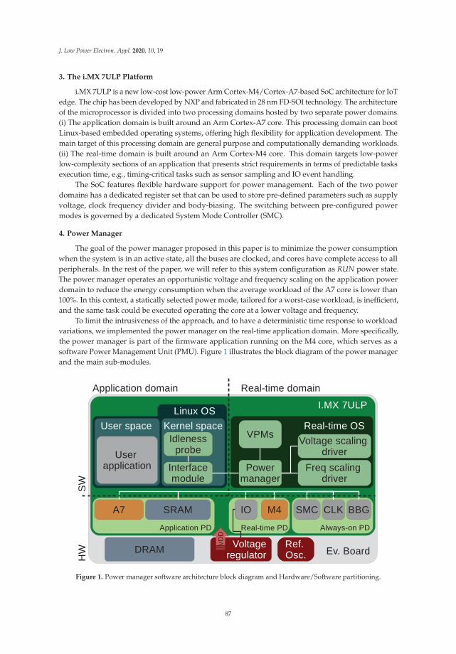
J. Low Power Electron. Appl. 2020, 10, 19
3. The i.MX 7ULP Platform
i.MX 7ULP is a new low-cost low-power Arm Cortex-M4/Cortex-A7-based SoC architecture for IoTedge. The chip has been developed by NXP and fabricated in 28 nm FD-SOI technology. The architectureof the microprocessor is divided into two processing domains hosted by two separate power domains.(i) The application domain is built around an Arm Cortex-A7 core. This processing domain can bootLinux-based embedded operating systems, offering high flexibility for application development. Themain target of this processing domain are general purpose and computationally demanding workloads.(ii) The real-time domain is built around an Arm Cortex-M4 core. This domain targets low-powerlow-complexity sections of an application that presents strict requirements in terms of predictable tasksexecution time, e.g., timing-critical tasks such as sensor sampling and IO event handling.
The SoC features flexible hardware support for power management. Each of the two powerdomains has a dedicated register set that can be used to store pre-defined parameters such as supplyvoltage, clock frequency divider and body-biasing. The switching between pre-configured powermodes is governed by a dedicated System Mode Controller (SMC).
4. Power Manager
The goal of the power manager proposed in this paper is to minimize the power consumptionwhen the system is in an active state, all the buses are clocked, and cores have complete access to allperipherals. In the rest of the paper, we will refer to this system configuration as RUN power state.The power manager operates an opportunistic voltage and frequency scaling on the application powerdomain to reduce the energy consumption when the average workload of the A7 core is lower than100%. In this context, a statically selected power mode, tailored for a worst-case workload, is inefficient,and the same task could be executed operating the core at a lower voltage and frequency.
To limit the intrusiveness of the approach, and to have a deterministic time response to workloadvariations, we implemented the power manager on the real-time application domain. More specifically,the power manager is part of the firmware application running on the M4 core, which serves as asoftware Power Management Unit (PMU). Figure 1 illustrates the block diagram of the power managerand the main sub-modules.
Figure 1. Power manager software architecture block diagram and Hardware/Software partitioning.
87

J. Low Power Electron. Appl. 2020, 10, 19
To operate the DVFS, we statically selected the RUN power mode. In this power state, the systemuses the main PLL to generate a reference clock frequency in the range from 800 MHz to 300 MHz;the forward body-bias can be applied to the transistors, the RAM is powered on, and the system cantolerate DVFS. In this scenario, we introduced multiple Virtual Power Modes (VPM). Each VPM is a setof values that the power manager uses to override configuration values for Voltage, clock Frequencyand Body-bias activation of the RUN power mode. The number of VPMs can be arbitrarily configuredby the user, their configuration values are stored in the M4 data memory.
The criterion on which the VPM of the system is switched is the idleness of the A7 core. Thisinformation is obtained directly from the operating system CPU statistics. The power managercompares the measured idleness with a user-specified target idleness, and determines how to adjustthe performance of the system to match the target idleness. Algorithm 1 describes the performanceadjustment procedure. The idleness observation time can vary in a range from 100 ms to 5 s dependingon the application requirements.
Algorithm 1 This pseudo-code procedure illustrates the steps that are performed by the power managerat every iteration of the power mode regulation.
1: while !new power mode request do2: wait for a new request3: end while4: if target idleness > curr. idleness then5: increase supply voltage6: while !Supply voltage change do7: wait8: end while9: increase clock freq.
10: while !clock freq. change do11: wait12: end while13: else14: decrease clock freq.15: while !clock freq. change do16: wait17: end while18: decrease supply voltage19: while !Supply voltage change do20: wait21: end while22: end if23: power mode transition complete
4.1. Real-Time Domain
The kernel of the power manager is part of the firmware running on the real-time domain,and it is constituted by 4 main sub-modules that operate synchronously to perform (i) the idlenessacquisition from the application domain, (ii) the target versus current idleness comparison, (iii) thepower mode selection and the power mode configuration registers modification, (iv) the voltage andthe frequency scaling.
4.2. Application Domain
The power manager uses the idleness of the core in a given time interval preceding the powermode regulation as a feedback signal. This information is made available by the operating system thatcollects statistics on the use of the core. To retrieve this information and transfer it to the real-timedomain, we developed (i) a module to track the idleness and (ii) a Linux-driver module that acts as aninterface with the power manager.
88
J. Low Power Electron. Appl. 2020, 10, 19
5. Experimental Setup
In this section, we describe the experimental setup for the measurements presented in Section 6.In our experiments, we focused on the dynamic reduction of the energy consumption of the applicationpower domain only, since it represents more than 90% of the power consumption of the entire SoC.Operating frequency and voltage of the real-time power domain have been statically selected as theminimum values that allow accomplishing the power management task.
In our power management implementation, we introduced six virtual power modes available fordynamic power mode selection. Table 1 reports the configuration values related to the core supplyvoltage and clock frequency of every VPM. Supply voltages have been arbitrarily chosen according to aquadratic curve, operating frequencies have been selected as the maximum ones achievable by the coreat the related supply voltages. To maximize performance, forward body-bias is active in all VPMs [15].To verify that the system was able to operate at a given frequency, we executed several benchmarks onthe core, selected among those provided by the stress-ng benchmark suite [16].
Table 1. Configuration values of Virtual Power Modes (VPM).
Power Mode ID VPM0 VPM1 VPM2 VPM3 VPM4 VPM5
Voltage [mV] 1100 1000 900 860 835 800
Frequency [MHz] 800 640 490 420 370 300
The power mode regulation period has been chosen as 5 s. This value can be modified toadjust responsiveness of the controller to the idleness variation, the minimum regulation period isapproximately of 100 ms; this value is bounded by the communication latency with the external voltageregulator hosted on the i.MX 7ULP evaluation board and does not constitute an intrinsic limitation ofthe i.MX 7ULP system.
To fully characterize the power manager and evaluate the benefits in terms of power saving weperformed the following measurements on the i.MX 7ULP evaluation board:
(i) we fixed the VPM, and we measured its power consumption. We performed the measurementsfor each of the VPMs reported in Table 1, and, at each VPM, we swept the CPU usage in a range of5% to 95%. The desired load of the core has been precisely changed by varying the number of taskslaunched in a fixed time period of 5 s. The use information of the core has been obtained by accessingthe core use and idleness statistic made available by the Linux kernel. In our experiment, we verifiedthat by executing a small number of tasks the core use was below 5%, and we linearly increased thenumber of task launched on the core within the reference period until the core use reached 95%.
(ii) we evaluated the power consumption at different workload levels when the controller isadjusting the power mode. We analyzed the response of the power manager when the target idlenesswas in a range of 5% to 95%, and similarly to the previous case, the workload on the core was swept ina range of 5% to 95%.
Section 6 shows the results of the two experiments; the power consumption has been measured atthe evaluation board 5 V power supply connector. The measurement conditions are the following:
• Operating temperature T = 25 °C• Test benchmark for operating frequency validation and power estimation = stress-ng test suite• Power measurement equipment = Keysight N6705B power analyzer (time resolution of 20 μs)
6. Results
In this section, we present the results in terms of power consumption reduction when the powermanager is active.
Figure 2a shows the power consumption of the i.MX 7ULP evaluation board when a VPM is fixed.From the static analysis, we can conclude that the dynamic power mode adaptation allows saving upto 28% of power when the system is in RUN mode, and in absence of core activity.
89
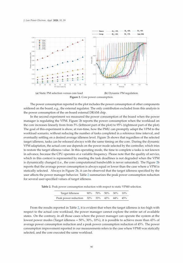
J. Low Power Electron. Appl. 2020, 10, 19
0 10 20 30 40 50 60 70 80 90 100
A7 Core load [%]
0.14
0.16
0.18
0.2
0.22
0.24
0.26
0.28
0.3
0.32
0.34
Pow
er c
onsu
mpt
ion
[W]
VPM0VPM1VPM2VPM3VPM4VPM5
(a) Static PM selection versus core load (b) Dynamic PM regulation.Figure 2. Core power consumption.
The power consumption reported in the plot includes the power consumption of other componentssoldered on the board, e.g., the external regulator. The only contribution excluded from this analysis isthe power consumption of the on-board external DRAM chip.
In the second experiment we measured the power consumption of the board when the powermanager is regulating the VPM. Figure 2b reports the power consumption when the workload onthe core increases linearly from from 5% (leftmost part of the plot) to 95% (rightmost part of the plot).The goal of this experiment is show, at run-time, how the PMU can promptly adapt the VPM to theworkload scenario, without reducing the number of tasks completed in a reference time interval, andeventually settling on a desired average idleness level. Figure 2b shows that regardless of the selectedtarget idleness, tasks can be released always with the same timing on the core. During the dynamicVPM adaptation, the actual core use depends on the power mode selected by the controller, which triesto restore the target idleness value. In this operating mode, the time to complete a tasks is not knownin advance, because the CPU operates at a variable frequency. Please note that the quality of service,which in this context is represented by meeting the task deadlines is not degraded when the VPMis dynamically changed (i.e., the core computational bandwidth is never saturated). The Figure 2breports that the average power consumption is always equal or lower than the case where a VPM isstatically selected. Always in Figure 2b, it can be observed that the target idleness specified by theuser affects the power manager behavior. Table 2 summarizes the peak power consumption reductionfor several user-specified values of target idleness.
Table 2. Peak power consumption reduction with respect to static VPM0 selection.
Target Idleness 90% 70% 50% 30% 10%
Peak power reduction 32% 33% 43% 44% 45%
From the results reported in Table 2, it is evident that when the target idleness is too high withrespect to the actual core workload, the power manager cannot explore the entire set of availablestates. On the contrary, in all those cases where the power manager can operate the system at thelowest power modes (Target idleness = 50%, 30%, 10%), it is possible to achieve more than 43% ofaverage power consumption reduction and a peak power consumption reduction of 45%. The powerconsumption improvement reported in our measurements refers to the case where VPM0 was staticallyselected, and the core executed the same workload.
90

J. Low Power Electron. Appl. 2020, 10, 19
In our experiment, we assumed that the number of operation performed at each task execution isconstant. In Figure 2b, we observe that every 5 s, a new set of task is released on the core, originating aspike in the power trace caused by the core wake-up. At each experiment run, which was performedwith a different target idleness, the core never saturated the computational bandwidth. Therefore,the number of task executed by the core was constant for all the experiments, while the powerconsumption significantly decreased, resulting in less energy consumed by the core.
7. Conclusions
In this paper, we presented the implementation of a power management unit capable of operatingan idleness aware dynamic power mode adaptation. We validated the proposed approach on a novellow-cost low-power heterogeneous MCU for IoT edge fabricated in 28 nm SOI technology. The proposedpower manager allows achieving a theoretical power consumption reduction higher than the 28% inabsence of core activity. We confirmed the expectations during the operation of the system, reportingmore than 43% of average power consumption reduction when the target idleness is selected accordingto the real idleness of the application, and a peak power consumption reduction of 45%.
Author Contributions: Conceptualization, L.B. and A.D.; methodology, H.F. and J.P.; software, A.D.; validation,A.D.; investigation, A.D.; data curation, A.D.; writing–original draft preparation, A.D.; writing–review and editing,A.D., H.F., J.P. and L.B.; supervision, H.F., J.P. and L.B.; project administration, H.F., J.P. and L.B. All authors haveread and agree to the published version of the manuscript.
Funding: Partially supported by NXP.
Conflicts of Interest: The authors declare no conflict of interest.
Abbreviations
The following abbreviations are used in this manuscript:IoT Internet of ThingsMCU Micro Controller UnitSoC System on ChipDVFS Dynamic voltage and Frequency ScalingISA Instruction Set ArchitectureFD-SOI Fully Depleted Silicon On InsulatorULP Ultra Low PowerCPU Central Processing UnitSMC System Mode ControllerPMU Power Management UnitPLL Phase Locked LoopVPM Virtual Power Mode
References
1. Conti, F.; Rossi, D.; Pullini, A.; Loi, I.; Benini, L. PULP: A Ultra-Low Power Parallel Accelerator forEnergy-Efficient and Flexible Embedded Vision. J. Signal Process. Syst. 2015, 84, 339–354. [CrossRef]
2. Rossi, D.; Pullini, A.; Loi, I.; Gautschi, M.; Gurkaynak, F.K.; Teman, A.; Constantin, J.; Burg, A.; Miro-Panades, I.;Beignè, E.; et al. 193 mops/mw @ 162 mops, 0.32 v to 1.15 v voltage range multi-core accelerator for energyefficient parallel and sequential digital processing. In Proceedings of the 2016 IEEE Symposium in Low-Powerand High-Speed Chips (COOL CHIPS XIX), Yokohama, Japan, 20–22 April 2016; pp. 1–3.
3. Qu, G. What is the limit of energy saving by dynamic voltage scaling? In Proceedings of the IEEE/ACMInternational Conference on Computer Aided Design, San Jose, CA, USA, 4–8 November 2001; pp. 560–563.
4. Rossi, D.; Pullini, A.; Loi, I.; Gautschi, M.; Gürkaynak, F.K.; Teman, A.; Constantin, J.; Burg, A.; Miro-Panades, I.;Beignè, E.; et al. Energy-efficient Near-Threshold Parallel Computing : The PULPv2 Cluster. IEEE Micro 2017,37, 20–31. [CrossRef]
5. Di Mauro, A.; Rossi, D.; Pullini, A.; Flatresse, P.; Benini, L. Independent Body-Biasing of P-N Transistors inan 28nm UTBB FD-SOI ULP Near-Threshold Multi-Core Cluster. In Proceedings of the 2018 IEEE SOI-3D-Subthreshold Microelectronics Technology Unified Conference (S3S), Burlingame, CA, USA, 15–18 October2018; pp. 1–3.
91
J. Low Power Electron. Appl. 2020, 10, 19
6. Di Mauro, A.; Rossi, D.; Pullini, A.; Flatresse, P.; Benini, L. Temperature and process-aware performancemonitoring and compensation for an ULP multi-core cluster in 28 nm UTBB FD-SOI technology. In Proceedingsof the 2017 27th International Symposium on Power and Timing Modeling, Optimization and Simulation(PATMOS), Thessaloniki, Greece, 25–27 September 2017; pp. 1–8.
7. Choi, K.; Soma, R.; Pedram, M. Fine-grained dynamic voltage and frequency scaling for precise energy andperformance tradeoff based on the ratio of off-chip access to on-chip computation times. IEEE Trans. Comput.Aided Des. Integr. Circuits Syst. 2005, 24, 18–28.
8. Seki, T.; Akui, S.; Seno, K.; Nakai, M.; Meguro, T.; Kondo, T.; Hashiguchi, A.; Kawahara, H.; Kumano, K.;Shimura, M. Dynamic voltage and frequency management for a low-power embedded microprocessor.IEICE Trans. Electron. 2005, 88, 520–527. [CrossRef]
9. Krishnaswamy, V.; Brooks, J.; Konstadinidis, G.; McAllister, C.; Pham, H.; Turullols, S.; Shin, J.L.; YangGong, Y.;Zhang, H. Fine-Grained Adaptive Power Management of the SPARC M7 processor. In Proceedings of the2015 IEEE International Solid-State Circuits Conference (ISSCC), San Francisco, CA, USA, 22–26 February2015; pp. 74–76.
10. Cheng, W.H.; Baas, B.M. Dynamic voltage and frequency scaling circuits with two supply voltages.In Proceedings of the IEEE International Symposium on Circuits and Systems, Seattle, WA, USA, 18–21 May2008; pp. 1236–1239.
11. Scordino, C.; Lipari, G. A resource reservation algorithm for power-aware scheduling of periodic and aperiodicreal-time tasks. IEEE Trans. Comput. 2006, 55, 1509–1522. [CrossRef]
12. Spiliopoulos, V.; Kaxiras, S.; Keramidas, G. Green governors: A framework for continuously adaptive dvfs.In Proceedings of the 2011 International Green Computing Conference and Workshops, Orlando, FL, USA,25–28 July 2011; pp. 1–8.
13. Juan, D.C.; Garg, S.; Park, J.; Marculescu, D. Learning the optimal operating point for many-core systemswith extended range voltage/frequency scaling. In Proceedings of the Ninth IEEE/ACM/IFIP InternationalConference on Hardware/Software Codesign and System Synthesis (CODES+ISSS ’13), Montreal, QC,Canada, 29 September–4 October 2013; IEEE Press: Piscataway, NJ, USA, 2013; pp. 8:1–8:10.
14. Pallipadi, V.; Starikovskiy, A. The Ondemand Governor. Linux Symp. 2006, 2, 223–238.15. Rossi, D.; Pullini, A.; Loi, I.; Gautschi, M.; Gürkaynak, F.K.; Bartolini, A.; Flatresse, P.; Benini, L. A 60 GOPS/W,
-1.8 v to 0.9 v body bias ULP cluster in 28 nm UTBB FD-SOI technology. Solid-State Electron. 2016, 117, 170–184.[CrossRef]
16. King, C.I. Stress-ng. Available online: https://github.com/ColinIanKing/stress-ng (accessed on 10 August 2018).
© 2020 by the authors. Licensee MDPI, Basel, Switzerland. This article is an open accessarticle distributed under the terms and conditions of the Creative Commons Attribution(CC BY) license (http://creativecommons.org/licenses/by/4.0/).
92
Journal of
Low Power Electronicsand Applications
Article
Low-Power Embedded System for Gait ClassificationUsing Neural Networks
Francisco Luna-Perejón *, Manuel Domínguez-Morales, Daniel Gutiérrez-Galán
and Antón Civit-Balcells
Architecture and Computer Technology Department, Universidad de Sevilla, E.T.S Ingeniería Informática,Reina Mercedes Avenue, 41012 Seville, Spain; [email protected] (M.D.-M.); [email protected] (D.G.-G.);[email protected] (A.C.-B.)* Correspondence: [email protected]
Received: 19 March 2020; Accepted: 17 April 2020; Published: 1 May 2020
Abstract: Abnormal foot postures can be measured during the march by plantar pressures in bothdynamic and static conditions. These detections may prevent possible injuries to the lower limbs likefractures, ankle sprain or plantar fasciitis. This information can be obtained by an embedded instrumentedinsole with pressure sensors and a low-power microcontroller. However, these sensors are placed insparse locations inside the insole, so it is not easy to correlate manually its values with the gait type; that iswhy a machine learning system is needed. In this work, we analyse the feasibility of integrating a machinelearning classifier inside a low-power embedded system in order to obtain information from the user’sgait in real-time and prevent future injuries. Moreover, we analyse the execution times, the powerconsumption and the model effectiveness. The machine learning classifier is trained using an acquireddataset of 3000+ steps from 6 different users. Results prove that this system provides an accuracy over99% and the power consumption tests obtains a battery autonomy over 25 days.
Keywords: machine learning; neural networks; gait analysis; embedded system
1. Introduction
Foot and ankle pain are very common in the population. Studies indicates that around 24% of peopleaged over 45 years report frequent foot pain [1]. Moreover, other studies indicate that more than 70% ofthe population over 65 years old present chronic foot pain [2].
It has also been demonstrated that abnormal foot postures and gait are associated with foot pain [3]as well as with lower limb injuries and pathologies [4]. Additionally, problems and disabilities associatedwith abnormal gait and foot posture include fractures, ankle sprain, pimple pain or plantar fasciitis,among others [5].
These previously named abnormalities due to bad foot postures have recently been related in severalexperiments to the pressure received at the base of the foot [4,6]. Therefore, a professional specialized infoot problems can perform a walking study of the patient’s footprint in order to detect these problems,prevent the injuries occasioned by prescribing insoles and/or indicate physical exercises to correct them.
For that reason, it is very important to characterize the static foot posture and the foot function witha gait analysis. In that concern, there are available various methods in the literature [7].
The classic gait study consists of walking in a straight line through a sensorized surface that emulatesa several meter long path—the surface measures and records the pressure obtained for each step during thegait for posterior analysis. The main problem using this mechanism is the psychological component—the
J. Low Power Electron. Appl. 2020, 10, 14; doi:10.3390/jlpea10020014 www.mdpi.com/journal/jlpea
93
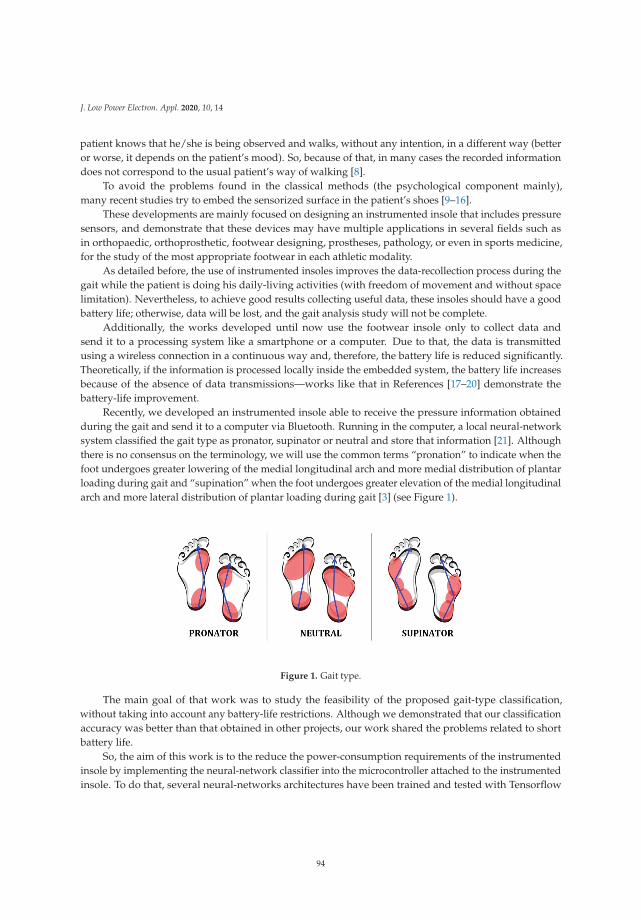
J. Low Power Electron. Appl. 2020, 10, 14
patient knows that he/she is being observed and walks, without any intention, in a different way (betteror worse, it depends on the patient’s mood). So, because of that, in many cases the recorded informationdoes not correspond to the usual patient’s way of walking [8].
To avoid the problems found in the classical methods (the psychological component mainly),many recent studies try to embed the sensorized surface in the patient’s shoes [9–16].
These developments are mainly focused on designing an instrumented insole that includes pressuresensors, and demonstrate that these devices may have multiple applications in several fields such asin orthopaedic, orthoprosthetic, footwear designing, prostheses, pathology, or even in sports medicine,for the study of the most appropriate footwear in each athletic modality.
As detailed before, the use of instrumented insoles improves the data-recollection process during thegait while the patient is doing his daily-living activities (with freedom of movement and without spacelimitation). Nevertheless, to achieve good results collecting useful data, these insoles should have a goodbattery life; otherwise, data will be lost, and the gait analysis study will not be complete.
Additionally, the works developed until now use the footwear insole only to collect data andsend it to a processing system like a smartphone or a computer. Due to that, the data is transmittedusing a wireless connection in a continuous way and, therefore, the battery life is reduced significantly.Theoretically, if the information is processed locally inside the embedded system, the battery life increasesbecause of the absence of data transmissions—works like that in References [17–20] demonstrate thebattery-life improvement.
Recently, we developed an instrumented insole able to receive the pressure information obtainedduring the gait and send it to a computer via Bluetooth. Running in the computer, a local neural-networksystem classified the gait type as pronator, supinator or neutral and store that information [21]. Althoughthere is no consensus on the terminology, we will use the common terms “pronation” to indicate when thefoot undergoes greater lowering of the medial longitudinal arch and more medial distribution of plantarloading during gait and “supination” when the foot undergoes greater elevation of the medial longitudinalarch and more lateral distribution of plantar loading during gait [3] (see Figure 1).
Figure 1. Gait type.
The main goal of that work was to study the feasibility of the proposed gait-type classification,without taking into account any battery-life restrictions. Although we demonstrated that our classificationaccuracy was better than that obtained in other projects, our work shared the problems related to shortbattery life.
So, the aim of this work is to the reduce the power-consumption requirements of the instrumentedinsole by implementing the neural-network classifier into the microcontroller attached to the instrumentedinsole. To do that, several neural-networks architectures have been trained and tested with Tensorflow
94

J. Low Power Electron. Appl. 2020, 10, 14
and Keras, using a database of 3000+ steps. We evaluate the effectiveness of the classifier in termsof the accuracy, among other metrics. After that, this architecture is compiled and integrated in theembedded system using STM32Cube.AI (artificial intelligence plugin used in STM32CubeIDE softwarefor STMicroelectronics microcontrollers) in order to check the correct behaviour when running onthe microcontroller, as well as to assess the power-consumption reduction when classifying with thelow-power microcontroller.
The rest of the paper is divided in the following way—first, the acquisition and evaluation processesare described in the Materials and Methods section, presenting the used embedded system , the collecteddatabase, and evaluated the neural-networks architectures. Next, the results obtained after the trainingprocess with the different neural-networks architectures in Keras, the classification from the neural networkdeployed into the embedded system and the power-consumption study are detailed and explained in theResults and Discussion section. Finally, conclusions are presented.
2. Materials and Methods
As detailed in the previous section, the system used in this work requires an instrumented insolecomposed of a set of force sensitive resistors (FSRs) and a microcontroller for the acquisition step and forthe final implementation.
Moreover, the main feature that makes the system to reduce drastically the power-consumptionrequirements consists in the implementation of the machine learning classifier in the microcontroller,avoiding the continuous data transmissions.
All these components and tools will be detailed in depth in this section, as well as the process followedfrom data acquisition to the final implementation.
2.1. Data Acquisition
The data registered for the gait analysis consists of a set of pressure measures obtained througha footwear insole connected to an embedded device. After an in depth study of the walking process andthe more adequate distribution of the sensors tested on previous works [21,22], seven FSRs are disposed indifferent parts of the foot. For each footstep, sensors samples at 50 hertz frequency since the first contactof the foot with the ground until the moment the foot is lifted. Thus, the information stored refers to themedium pressure received by each sensor during each step. These values are normalized after each stepends using the sensor’s value with the highest pressure received as 100% pressure and modifying theother sensors’ values to a percentage value relative to that sensor.
Next, both the footwear insole and the dataset obtained after the acquisition phase are detailed.
2.1.1. Footwear Insole
The hardware system used for the acquisition is based on a low-power consumption microcontroller,seven force sensitive resistors (FSRs) and a low-energy Bluetooth module. The selected microcontroller wasa STMicroelectronics MCU used for the acquisition and testing phases (model STM32L476RG, operating ata frequency up to 80 MHz, with 1 Mbyte of flash memory and 128 Kbytes of SRAM), with features thatallow real-time capabilities, digital signal processing and low-power operation. The FSRs were connectedto the analog inputs of the microcontroller using a voltage divider with a 10 KΩ resistor. These sensorsprovide information about the maximum pressure point and the load forces. Finally, a HM-10 BLE(Bluetooth Low-Energy) module was connected to the microcontroller as a wireless communication portto send the information to the computer (see Figure 2).
95
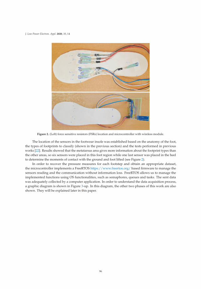
J. Low Power Electron. Appl. 2020, 10, 14
Figure 2. (Left) force sensitive resistors (FSRs) location and microcontroller with wireless module.
The location of the sensors in the footwear insole was established based on the anatomy of the foot,the types of footprints to classify (shown in the previous section) and the tests performed in previousworks [22]. Results showed that the metatarsus area gives more information about the footprint types thanthe other areas, so six sensors were placed in this foot region while one last sensor was placed in the heelto determine the moments of contact with the ground and foot lifted (see Figure 2).
In order to recover the pressure measures for each footstep and obtain an appropriate dataset,the microcontroller implements a FreeRTOS https://www.freertos.org/ based firmware to manage thesensors reading and the communication without information loss. FreeRTOS allows us to manage theimplemented functions using OS functionalities, such as semaphores, queues and tasks. The sent datawas adequately collected by a computer application. In order to understand the data acquisition process,a graphic diagram is shown in Figure 3-up. In this diagram, the other two phases of this work are alsoshown. They will be explained later in this paper.
96
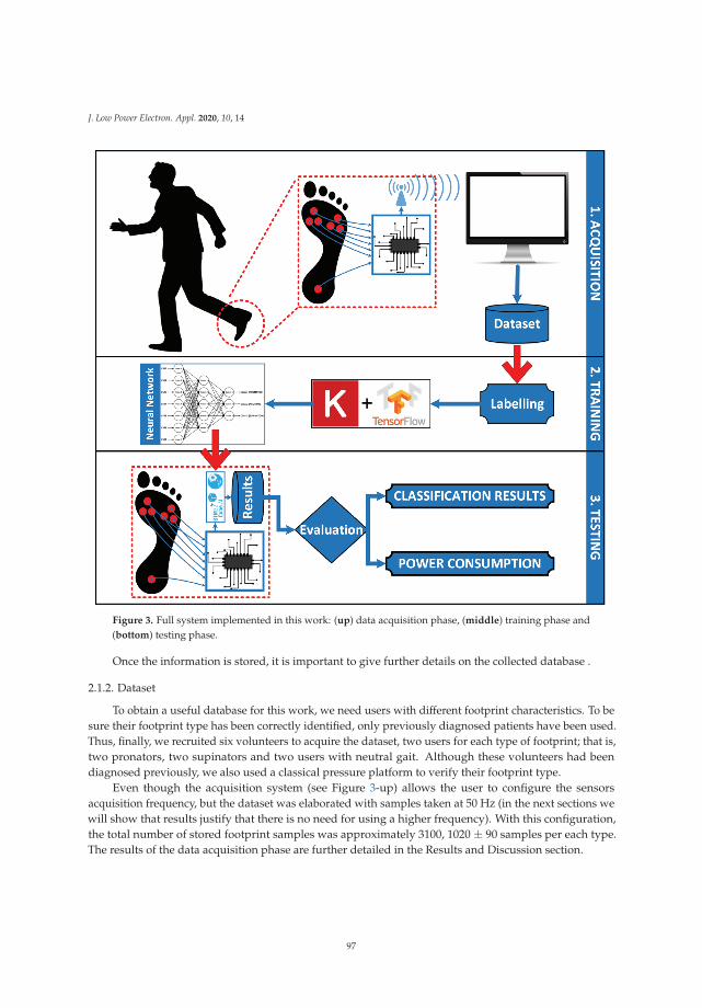
J. Low Power Electron. Appl. 2020, 10, 14
Figure 3. Full system implemented in this work: (up) data acquisition phase, (middle) training phase and(bottom) testing phase.
Once the information is stored, it is important to give further details on the collected database .
2.1.2. Dataset
To obtain a useful database for this work, we need users with different footprint characteristics. To besure their footprint type has been correctly identified, only previously diagnosed patients have been used.Thus, finally, we recruited six volunteers to acquire the dataset, two users for each type of footprint; that is,two pronators, two supinators and two users with neutral gait. Although these volunteers had beendiagnosed previously, we also used a classical pressure platform to verify their footprint type.
Even though the acquisition system (see Figure 3-up) allows the user to configure the sensorsacquisition frequency, but the dataset was elaborated with samples taken at 50 Hz (in the next sections wewill show that results justify that there is no need for using a higher frequency). With this configuration,the total number of stored footprint samples was approximately 3100, 1020 ± 90 samples per each type.The results of the data acquisition phase are further detailed in the Results and Discussion section.
97
J. Low Power Electron. Appl. 2020, 10, 14
2.2. Artificial Neural Network Classifier
Artificial Neural Networks (ANNs) have been used in several works recently to find the relationshipbetween some input data and the desired response at the system output (called the system’s inferenceor classification). This machine learning mechanism is very useful in applications where there are largeamounts of input data and the relationship between that data and the expected output cannot be easilyappreciated [23]. Thus, after an initial ’training’ phase, the ANN is configured with a set of weights atboth outputs and inputs of the different neuron layers with which the desired outputs can be obtained.ANNs have been demonstrated to obtain very good results in previous works, especially when used asa supervised machine learning method [24–26].
Their structure, based solely on arithmetic operations (except perhaps in inference phases inclassification problems), allows them to be combined with other architectures, making them a fundamentalcomponent in several Deep Learning algorithms. It is also possible to create very efficient implementations,which can be optimized for low performance devices, such as low-power microcontrollers [27]. This factallows acceptable execution times with very low power consumption. In this section we describe theANN architectures analysed in terms of effectiveness, as well as their performance when embedded ina low-power device.
2.2.1. Architecture Design
An ANN architecture with three layers is used in this gait classification study (see Figure 4). The firstlayer, that is, the input, contains seven nodes that receive information from the different FSRs, for eachfootstep. The last layer, the output, consisting of three nodes that return the degree of confidence ofa sample to belong to one of the three footprint classes (supinator, pronator or neutral). A final outputfunction called softmax is used. It implements a multi-class sigmoid and is typically used to normalize theresults of the network output layer, limiting each output to the 0 to 1 range. The sum of the values of all theoutput nodes for this function is always 1. This allows us to interpret the output directly as a probabilityor confidence. Thus, the predicted class would be that with a greater confidence. The intermediate layer,called the hidden layer, is connected to the input and the output layers. Each node of this layer receivesthe information of all the seven input nodes, processes it and transmits its result to the three nodes inthe output layer. Thus it is called a Fully Connected or Dense layer. In this study, architectures withdifferent numbers of nodes in the hidden layer were considered, in order to reduce the complexity ofthe architecture while maintaining a good classification effectiveness. Therefore we have to look fora high-accuracy network with low complexity to implement it inside a microcontroller as this implies lessmemory usage and a smaller power consumption.
In this study, TensorFlow https://www.tensorflow.org together with Keras https://keras.io/ havebeen used to implement, train and test the architectures with the previously detailed dataset (seeFigure 3-middle for a global description of the training phase). Tensorflow is a library created by Google fordistributed numerical computation, that allows to design, train, evaluate and run models based on neuralnetworks. Keras is a high-level API that simplifies model implementation with Tensorflow, by efficientlymanaging the connection between model layers and simplifying the Tensorflow code. The resultingmodels are compatible with STM32Cube utilities, allowing the creation of a C-compiled version that canbe embedded in STM32 microcontrollers.
98
J. Low Power Electron. Appl. 2020, 10, 14
Figure 4. Artificial Neural Network (ANN) architecture used in the study for classification.
2.2.2. Embedded Model Analysis
After the acquisition and training phases (see Figure 3-up and Figure 3-middle, respectively), the ANNis integrated into the embedded system in order to evaluate whether it provides the same effectivenessresults as the original implementation on a general-purpose computer, as well as the improvements inenergy consumption. For that purpose, STM32CubeIDE development environment https://www.st.com/en/development-tools/stm32cubeide.html was used. It provides tools for power consumption analysiswhen using different components and modules. Additionally, their STM32Cube.AI expansion plug-inhttps://www.st.com/en/embedded-software/x-cube-ai.html allows to generate C-compiled versions ofpre-trained Neural Networks models, optimized for STM32 microcontrollers.
To verify that the model effectiveness is maintained after conversion to a C-compiled version andintegration into the microcontroller, we compared the output confidence results for each class with thoseobtained with the original Keras model. We used the same MCU that the one used for the acquisitionphase for the integration and performance analysis of the trained models.
For the power efficiency analysis, two different scenarios were considered (see Figure 5). In thefirst one, the embedded system collects data from the sensors at 50Hz and sends it via Bluetooth (every20 ms); the information is received by the host, which processes and classifies it using an external ANNclassifier (this scenario is similar than the one used for the acquisition phase, but now the ANN classifier isimplemented in the host). In this case, the system spends almost 4ms for each data transmission (sending56 bytes at 115,200 bauds), which is 20% of the total time; and, moreover, the transmission process takesmore than 43 mA of power consumption (much more than the average power consumption of the system).
In the second scenario, the classification process is done inside the embedded system with the internalANN implementation. The information read from the sensors is processed and stored internally and,only once per step, the ANN classifies the footstep type and, after that, the classification result is transmittedto the host using Bluetooth. Two main improvements are obtained in this second scenario—first,the transmitted data size is significantly reduced (from 56 bytes to 3 bytes) and, thus, the transmission
99
J. Low Power Electron. Appl. 2020, 10, 14
time is much lower that in the first scenario (0.2 ms); and, second, the transmission is only done aftereach classification (only one per step), so the number of transmissions is much less than that in the firstscenario. However, the number of transmissions depends on the gait cadence of the user, so it must bestudied in depth.
Figure 5. Two scenarios proposed for power consumption analysis.
To easily understand both scenarios, the implemented firmwares are described. The first one (seeFigure 6-left) was used to acquire the data for the database and it was also used as “scenario 1” for thefinal power-consumption comparison. The second one (see Figure 6-right) is used for the embedded ANNimplementation and hence it corresponds to “scenario 2” in the testing phase.
Figure 6. Implemented Firmwares for the acquisition (left) and testing phase (right).
The firmware implemented in the MCU for the acquisition phase is a FreeRTOS based implementationthat allows a bi-directional serial communication with the bluetooth module (process 1 for reception
100
J. Low Power Electron. Appl. 2020, 10, 14
and process 3 for transmission) and a periodic sensor readings with data transformation (process 2),using a binary semaphore and a queue to communicate between these process. So, in the acquisition phase,there is no recording inside the MCU memory; but, after each reading, the data is packed and sent to anexternal computer where the information is stored in a database.
And, for the testing phase, the implemented firmware is also FreeRTOS based and uses periodicreadings, value normalization and performs an ANN classification after each steps ends. The result of thisclassification is transmitted (once per step) to the external computer.
3. Results and Discussion
In this section, the results obtained at the end of each phase are detailed. For the acquisition phase (seeFigure 3-up), the collected dataset is presented. For the training step (see Figure 3-middle), the classificationresults are detailed and, finally, the embedded model accuracy and the power consumption study arepresented as results of the testing phase (see Figure 3-bottom).
3.1. Dataset
The dataset used in this study was split for training and assessment purposes. We used the Hold-outtechnique, by randomly selecting a sample subset for the training of the models, and using the remainingsubset to validate the model performance. A subset with the 85% of dataset samples was used for training,while the remaining 15% subset was used for evaluation. The distribution was made to ensure that therewas a balanced percentage of each type of footprint in both subsets. Table 1 shows the distribution.
Table 1. Dataset distribution for each subset.
Subset Neutral Pronator Supinator Total
Total 1067 1129 928 3124Training 917 955 784 2656Test 150 174 144 468
3.2. ANN Model Assessment
This section presents the trained ANN architectures, their implementation and training specificationsand the effectiveness evaluation results.
3.2.1. ANN Architectures and Parameters
We analyse the architecture introduced in Section 2.2.1 with different numbers of nodes in its hiddenlayer. In previous studies, 5 hidden nodes were used in the hidden layer, based on [28]. For the currentanalysis, we assess the effectiveness by reducing the number of nodes looking for an improvement ofclassification times and power consumption reduction. Sigmoid function was used as activation functionfor the nodes in the hidden layer, while Rectified Linear Unit (ReLU) function was used for the output layernodes. The model training was performed with a learning rate of 0.001, a batch size of 8 and 75 epochs.The used optimizer was a Root Mean Square Prop (RMSProp).
3.2.2. Effectiveness Results
We compared the effectiveness using different metrics—accuracy, sensitivity (also named macrorecall), specificity, macro precision and macro F1-score [29]. This last metric measures the relation is theharmonic mean of macro precision and macro recall.
101
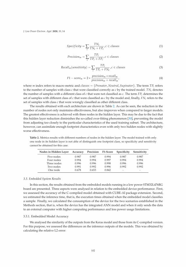
J. Low Power Electron. Appl. 2020, 10, 14
Speci f icity = ∑c
TNc
TNc + FPc, c ∈ classes (1)
Precisionm = ∑c
TPc
TPc + FPc, c ∈ classes (2)
Recallm(sensitivity) = ∑c
TPc
TPc + FNc, c ∈ classes (3)
F1 − scorem = 2 ∗ precisionm ∗ recallmprecisionm + recallm
, (4)
where m index refers to macro metric and classes = {Pronator, Neutral, Supinator}. The term TPc refersto the number of samples with class c that were classified correctly as c by the trained model. TNc denotesthe number of samples with a different class of c that were not classified as c. The term FPc determines theset of samples with different class of c that were classified as c by the model and, finally, FNc refers to theset of samples with class c that were wrongly classified as other different class.
The results obtained with each architecture are shown in Table 2. As can be seen, the reduction in thenumber of nodes not only maintains effectiveness, but also improves when compared to larger models.The greatest effectiveness is achieved with three nodes in the hidden layer. This may be due to the fact thatthis hidden layer reduction diminishes the so-called over-fitting phenomenon [30], preventing the modelfrom adjusting too closely to the particular characteristics of the used training subset. The architecture,however, can assimilate enough footprint characteristics even with only two hidden nodes with slightlyworse effectiveness.
Table 2. Metrics results with different numbers of nodes in the hidden layer. The model trained with onlyone node in its hidden layer is not able of distinguish one footprint class, so specificity and sensitivitycannot be obtained for this case.
Nodes in Hidden Layer Accuracy Precision F1-Score Specificity Sensitivity
Five nodes 0.987 0.987 0.994 0.987 0.987Four nodes 0.994 0.994 0.997 0.994 0.994Three nodes 0.996 0.996 0.998 0.996 0.996Two nodes 0.991 0.992 0.996 0.992 0.992One node 0.678 0.653 0.842 - -
3.3. Embedded System Results
In this section, the results obtained from the embedded models running in a low power STM32L476RGboard are presented. Three aspects were analysed in relation to the embedded device performance. First,we assessed the accuracy of the C-compiled model obtained with CUBE-AI package extension. Second,we estimated the inference time, that is, the execution times obtained when the embedded model classifiesa sample. Finally, we calculated the consumption of the device for the two scenarios established in theMethods section, that is, when the device has the integrated ANN model and when it only sends the datato an external computer with higher computing performance and less power usage limitations.
3.3.1. Embedded Model Accuracy
We analysed the similarity of the outputs from the Keras model and those from its C-compiled version.For this purpose, we assessed the differences on the inference outputs of the models. This was obtained bycalculating the relative L2 error:
102
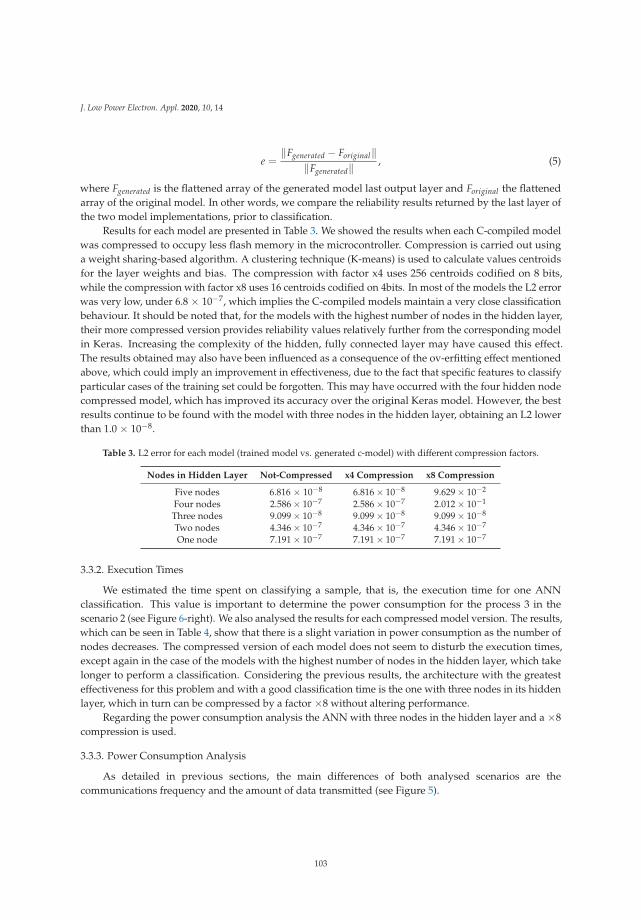
J. Low Power Electron. Appl. 2020, 10, 14
e =‖Fgenerated − Foriginal‖
‖Fgenerated‖ , (5)
where Fgenerated is the flattened array of the generated model last output layer and Foriginal the flattenedarray of the original model. In other words, we compare the reliability results returned by the last layer ofthe two model implementations, prior to classification.
Results for each model are presented in Table 3. We showed the results when each C-compiled modelwas compressed to occupy less flash memory in the microcontroller. Compression is carried out usinga weight sharing-based algorithm. A clustering technique (K-means) is used to calculate values centroidsfor the layer weights and bias. The compression with factor x4 uses 256 centroids codified on 8 bits,while the compression with factor x8 uses 16 centroids codified on 4bits. In most of the models the L2 errorwas very low, under 6.8 × 10⁻⁷, which implies the C-compiled models maintain a very close classificationbehaviour. It should be noted that, for the models with the highest number of nodes in the hidden layer,their more compressed version provides reliability values relatively further from the corresponding modelin Keras. Increasing the complexity of the hidden, fully connected layer may have caused this effect.The results obtained may also have been influenced as a consequence of the ov-erfitting effect mentionedabove, which could imply an improvement in effectiveness, due to the fact that specific features to classifyparticular cases of the training set could be forgotten. This may have occurred with the four hidden nodecompressed model, which has improved its accuracy over the original Keras model. However, the bestresults continue to be found with the model with three nodes in the hidden layer, obtaining an L2 lowerthan 1.0 × 10⁻⁸.
Table 3. L2 error for each model (trained model vs. generated c-model) with different compression factors.
Nodes in Hidden Layer Not-Compressed x4 Compression x8 Compression
Five nodes 6.816 × 10⁻⁸ 6.816 × 10⁻⁸ 9.629 × 10⁻²
Four nodes 2.586 × 10⁻⁷ 2.586 × 10⁻⁷ 2.012 × 10⁻¹
Three nodes 9.099 × 10⁻⁸ 9.099 × 10⁻⁸ 9.099 × 10⁻⁸
Two nodes 4.346 × 10⁻⁷ 4.346 × 10⁻⁷ 4.346 × 10⁻⁷
One node 7.191 × 10⁻⁷ 7.191 × 10⁻⁷ 7.191 × 10⁻⁷
3.3.2. Execution Times
We estimated the time spent on classifying a sample, that is, the execution time for one ANNclassification. This value is important to determine the power consumption for the process 3 in thescenario 2 (see Figure 6-right). We also analysed the results for each compressed model version. The results,which can be seen in Table 4, show that there is a slight variation in power consumption as the number ofnodes decreases. The compressed version of each model does not seem to disturb the execution times,except again in the case of the models with the highest number of nodes in the hidden layer, which takelonger to perform a classification. Considering the previous results, the architecture with the greatesteffectiveness for this problem and with a good classification time is the one with three nodes in its hiddenlayer, which in turn can be compressed by a factor ×8 without altering performance.
Regarding the power consumption analysis the ANN with three nodes in the hidden layer and a ×8compression is used.
3.3.3. Power Consumption Analysis
As detailed in previous sections, the main differences of both analysed scenarios are thecommunications frequency and the amount of data transmitted (see Figure 5).
103
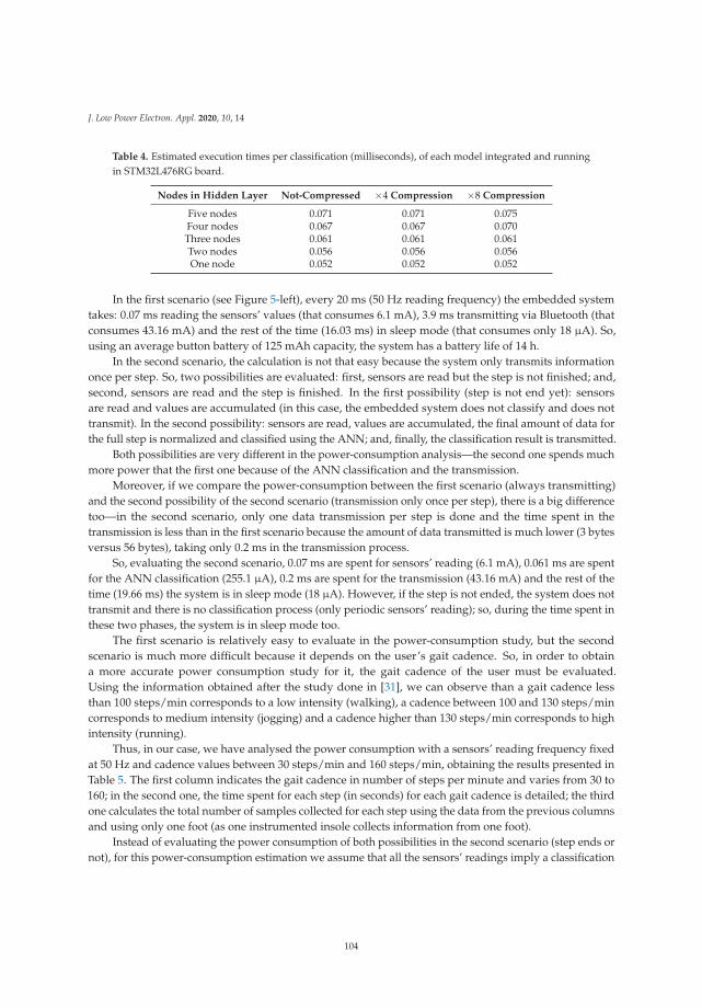
J. Low Power Electron. Appl. 2020, 10, 14
Table 4. Estimated execution times per classification (milliseconds), of each model integrated and runningin STM32L476RG board.
Nodes in Hidden Layer Not-Compressed ×4 Compression ×8 Compression
Five nodes 0.071 0.071 0.075Four nodes 0.067 0.067 0.070Three nodes 0.061 0.061 0.061Two nodes 0.056 0.056 0.056One node 0.052 0.052 0.052
In the first scenario (see Figure 5-left), every 20 ms (50 Hz reading frequency) the embedded systemtakes: 0.07 ms reading the sensors’ values (that consumes 6.1 mA), 3.9 ms transmitting via Bluetooth (thatconsumes 43.16 mA) and the rest of the time (16.03 ms) in sleep mode (that consumes only 18 μA). So,using an average button battery of 125 mAh capacity, the system has a battery life of 14 h.
In the second scenario, the calculation is not that easy because the system only transmits informationonce per step. So, two possibilities are evaluated: first, sensors are read but the step is not finished; and,second, sensors are read and the step is finished. In the first possibility (step is not end yet): sensorsare read and values are accumulated (in this case, the embedded system does not classify and does nottransmit). In the second possibility: sensors are read, values are accumulated, the final amount of data forthe full step is normalized and classified using the ANN; and, finally, the classification result is transmitted.
Both possibilities are very different in the power-consumption analysis—the second one spends muchmore power that the first one because of the ANN classification and the transmission.
Moreover, if we compare the power-consumption between the first scenario (always transmitting)and the second possibility of the second scenario (transmission only once per step), there is a big differencetoo—in the second scenario, only one data transmission per step is done and the time spent in thetransmission is less than in the first scenario because the amount of data transmitted is much lower (3 bytesversus 56 bytes), taking only 0.2 ms in the transmission process.
So, evaluating the second scenario, 0.07 ms are spent for sensors’ reading (6.1 mA), 0.061 ms are spentfor the ANN classification (255.1 μA), 0.2 ms are spent for the transmission (43.16 mA) and the rest of thetime (19.66 ms) the system is in sleep mode (18 μA). However, if the step is not ended, the system does nottransmit and there is no classification process (only periodic sensors’ reading); so, during the time spent inthese two phases, the system is in sleep mode too.
The first scenario is relatively easy to evaluate in the power-consumption study, but the secondscenario is much more difficult because it depends on the user’s gait cadence. So, in order to obtaina more accurate power consumption study for it, the gait cadence of the user must be evaluated.Using the information obtained after the study done in [31], we can observe than a gait cadence lessthan 100 steps/min corresponds to a low intensity (walking), a cadence between 100 and 130 steps/mincorresponds to medium intensity (jogging) and a cadence higher than 130 steps/min corresponds to highintensity (running).
Thus, in our case, we have analysed the power consumption with a sensors’ reading frequency fixedat 50 Hz and cadence values between 30 steps/min and 160 steps/min, obtaining the results presented inTable 5. The first column indicates the gait cadence in number of steps per minute and varies from 30 to160; in the second one, the time spent for each step (in seconds) for each gait cadence is detailed; the thirdone calculates the total number of samples collected for each step using the data from the previous columnsand using only one foot (as one instrumented insole collects information from one foot).
Instead of evaluating the power consumption of both possibilities in the second scenario (step ends ornot), for this power-consumption estimation we assume that all the sensors’ readings imply a classification
104
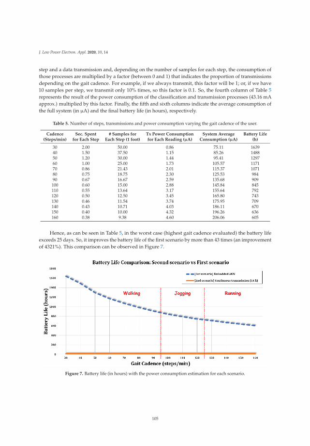
J. Low Power Electron. Appl. 2020, 10, 14
step and a data transmission and, depending on the number of samples for each step, the consumption ofthose processes are multiplied by a factor (between 0 and 1) that indicates the proportion of transmissionsdepending on the gait cadence. For example, if we always transmit, this factor will be 1; or, if we have10 samples per step, we transmit only 10% times, so this factor is 0.1. So, the fourth column of Table 5represents the result of the power consumption of the classification and transmission processes (43.16 mAapprox.) multiplied by this factor. Finally, the fifth and sixth columns indicate the average consumption ofthe full system (in μA) and the final battery life (in hours), respectively.
Table 5. Number of steps, transmissions and power consumption varying the gait cadence of the user.
Cadence Sec. Spent # Samples for Tx Power Consumption System Average Battery Life(Steps/min) for Each Step Each Step (1 foot) for Each Reading (μA) Consumption (μA) (h)
30 2.00 50.00 0.86 75.11 163940 1.50 37.50 1.15 85.26 148850 1.20 30.00 1.44 95.41 129760 1.00 25.00 1.73 105.57 117170 0.86 21.43 2.01 115.37 107180 0.75 18.75 2.30 125.53 98490 0.67 16.67 2.59 135.68 909100 0.60 15.00 2.88 145.84 845110 0.55 13.64 3.17 155.64 792120 0.50 12.50 3.45 165.80 743130 0.46 11.54 3.74 175.95 709140 0.43 10.71 4.03 186.11 670150 0.40 10.00 4.32 196.26 636160 0.38 9.38 4.60 206.06 605
Hence, as can be seen in Table 5, in the worst case (highest gait cadence evaluated) the battery lifeexceeds 25 days. So, it improves the battery life of the first scenario by more than 43 times (an improvementof 4321%). This comparison can be observed in Figure 7.
Figure 7. Battery life (in hours) with the power consumption estimation for each scenario.
105
J. Low Power Electron. Appl. 2020, 10, 14
The results presented in Figure 7 show that the higher the gait cadence, the lower the battery life is.Despite this, the life of the used battery (125 mAh) even for cases in which the user is running high enoughto allow a biomechanical gait study without recharges.
4. Conclusions
In this work, a performance analysis of a low-power footwear insole for the detection of abnormalfoot postures is presented. The device implements an embedded Machine Learning model based onANN for real-time footprint type inference. The inputs of the model consist of average FSR measuresobtained during a footstep, and the outputs correspond to the three gait types described in the Introductionsection—pronator, supinator and neutral.
First, a model study was performed. The effectiveness of the ANN architecture, consisting of threeneural layers, was assessed using a different number of nodes in the hidden layer. The architecturewith three nodes obtained the best results, with effectiveness metrics above 99.6%. The architectureswith a greater number of nodes showed slightly less classification ability, possibly due to overfitting thetraining dataset.
Finally, as the main point of the study, a complete analysis of the classifier performance has beenperformed when it is integrated into a low-power embedded device. The L2 error obtained whencomparing the Keras and the C-compiled model outputs showed that the conversion does not havea significant impact on the effectiveness of the model, even when the model is compressed, thus savingmemory space on the microcontroller. This can be an important aspect if we intend to include other modelswith different functionalities in the device in future works. Regarding the inference execution times,the best model is able to classify a footstep sample in 0.61 ms, even when it is compressed. This is muchless than the time needed to read a sample of the insole sensors, thereby achieving real-time execution.Based on this, and considering that the classifier execution and result transmission only take place whena full step is performed, the battery life estimation is over 25 days (considering the higher gait cadence).
Author Contributions: Conceptualization, M.D.-M., D.G.-G. and A.C.-B.; methodology, F.L.-P., M.D.-M. and A.C.-B.;software, F.L.-P. and D.G.-G.; validation, F.L.-P., M.D.-M. and A.C.-B.; investigation, F.L.-P., D.G.-G. and M.D.-M.;resources, F.L.-P. and M.D.-M.; writing–original draft preparation, F.L.-P., D.G.-G. and M.D.-M.; writing–review andediting, D.G.-G. and A.C.-B.; supervision, M.D.-M. and A.C.-B.; funding acquisition, A.C.-B. All authors have readand agreed to the published version of the manuscript.
Funding: This research was funded by the Robotics and Computer Technology Lab. (RTC) of the Universidad deSevilla, Spain.
Acknowledgments: This work has been supported by the Robotics and Computer Technology Lab. (RTC) of theUniversidad de Sevilla, Spain.
Conflicts of Interest: The authors declare no conflict of interest.
Abbreviations
The following abbreviations are used in this manuscript:
OS Operating SystemANN Artificial Neural NetworkFSR Force Sensitive ResistorsBLE Bluetooth Low EnergyMCU MicrocontrollerReLU Rectified Linear Unit
106
J. Low Power Electron. Appl. 2020, 10, 14
References
1. Thomas, M.J.; Roddy, E.; Zhang, W.; Menz, H.B.; Hannan, M.T.; Peat, G.M. The population prevalence of footand ankle pain in middle and old age: A systematic review. Pain 2011, 152, 2870–2880. [CrossRef]
2. Menz, H.B. Chronic foot pain in older people. Maturitas 2016, 91, 110–114. [CrossRef] [PubMed]3. Menz, H.B.; Dufour, A.B.; Riskowski, J.L.; Hillstrom, H.J.; Hannan, M.T. Association of planus foot posture
and pronated foot function with foot pain: The Framingham foot study. Arthritis Care Res. 2013, 65, 1991–1999.[CrossRef]
4. Buldt, A.K.; Allan, J.J.; Landorf, K.B.; Menz, H.B. The relationship between foot posture and plantar pressureduring walking in adults: A systematic review. Gait Posture 2018, 62, 56–67. [CrossRef] [PubMed]
5. Perry, J.; Davids, J.R. Gait analysis: Normal and pathological function. J. Pediatr. Orthop. 1992, 12, 815. [CrossRef]6. Buldt, A.K.; Forghany, S.; Landorf, K.B.; Levinger, P.; Murley, G.S.; Menz, H.B. Foot posture is associated with
plantar pressure during gait: A comparison of normal, planus and cavus feet. Gait Posture 2018, 62, 235–240.[CrossRef]
7. Razeghi, M.; Batt, M.E. Foot type classification: A critical review of current methods. Gait Posture 2002,15, 282–291. [CrossRef]
8. Frelih, N.G.; Podlesek, A.; Babic, J.; Geršak, G. Evaluation of psychological effects on human postural stability.Measurement 2017, 98, 186–191. [CrossRef]
9. Morris, S.J.; Paradiso, J.A. Shoe-integrated sensor system for wireless gait analysis and real-time feedback.In Proceedings of the Second Joint 24th Annual Conference and the Annual Fall Meeting of the BiomedicalEngineering Society, Houston, TX, USA, 23–26 October 2002; Volume 3, pp. 2468–2469.
10. Bamberg, S.J.M.; Benbasat, A.Y.; Scarborough, D.M.; Krebs, D.E.; Paradiso, J.A. Gait analysis usinga shoe-integrated wireless sensor system. IEEE Trans. Inf. Technol. Biomed. 2008, 12, 413–423. [CrossRef]
11. Shu, L.; Hua, T.; Wang, Y.; Li, Q.; Feng, D.D.; Tao, X. In-shoe plantar pressure measurement and analysis systembased on fabric pressure sensing array. IEEE Trans. Inf. Technol. Biomed. 2010, 14, 767–775.
12. Wahab, Y.; Mazalan, M.; Bakar, N.; Anuar, A.; Zainol, M.; Hamzah, F. Low power shoe integrated intelligentwireless gait measurement system. J. Phys. Conf. Ser. IOP Publ. 2014, 495, 13–14. [CrossRef]
13. Crea, S.; Donati, M.; De Rossi, S.M.M.; Oddo, C.M.; Vitiello, N. A wireless flexible sensorized insole for gaitanalysis. Sensors 2014, 14, 1073–1093. [CrossRef] [PubMed]
14. Talib, N.; Rahman, M.; Najib, A.; Noor, M. Implementation of Piezoelectric Sensor in Gait Measurement System.In Proceedings of the 2018 8th IEEE International Conference on Control System, Computing and Engineering(ICCSCE), Penang, Malaysia, 23–25 November 2018; pp. 20–25.
15. Oshimoto, T.; Abe, I.; Kikuchi, T.; Chijiwa, N.; Yabuta, T.; Tanaka, K.; Asaumi, Y. Gait Measurement for WalkingSupport Shoes with Elastomer-Embedded Flexible Joint. In Proceedings of the 2019 IEEE/SICE InternationalSymposium on System Integration (SII), Paris, France, 14–16 January 2019; pp. 537–542.
16. Ngamsuriyaroj, S.; Chira-Adisai, W.; Somnuk, S.; Leksunthorn, C.; Saiphim, K. Walking gait measurement andanalysis via knee angle movement and foot plantar pressures. In Proceedings of the 2018 15th International JointConference on Computer Science and Software Engineering (JCSSE), Nakhonpathom, Thailand, 11–13 July 2018;pp. 1–6.
17. Dominguez-Morales, J.P.; Rios-Navarro, A.; Dominguez-Morales, M.; Tapiador-Morales, R.; Gutierrez-Galan,D.; Cascado-Caballero, D.; Jimenez-Fernandez, A.; Linares-Barranco, A. Wireless sensor network for wildlifetracking and behavior classification of animals in Doñana. IEEE Commun. Lett. 2016, 20, 2534–2537. [CrossRef]
18. Henkel, J.; Pagani, S.; Amrouch, H.; Bauer, L.; Samie, F. Ultra-low power and dependability for IoT devices(Invited paper for IoT technologies). In Proceedings of the Design, Automation & Test in Europe Conference &Exhibition (DATE), Lausanne, Switzerland, 27–31 March 2017; pp. 954–959.
19. Andres-Maldonado, P.; Ameigeiras, P.; Prados-Garzon, J.; Ramos-Munoz, J.J.; Lopez-Soler, J.M. Optimized LTEdata transmission procedures for IoT: Device side energy consumption analysis. In Proceedings of the 2017IEEE International Conference on Communications Workshops (ICC Workshops), Paris, France, 21–25 May 2017;pp. 540–545.
107
J. Low Power Electron. Appl. 2020, 10, 14
20. Deepu, C.J.; Heng, C.H.; Lian, Y. A hybrid data compression scheme for power reduction in wireless sensors forIoT. IEEE Trans. Biomed. Circuits Syst. 2016, 11, 245–254. [CrossRef]
21. Domínguez-Morales, M.J.; Luna-Perejón, F.; Miró-Amarante, L.; Hernández-Velázquez, M.; Sevillano-Ramos, J.L.Smart Footwear Insole for Recognition of Foot Pronation and Supination Using Neural Networks. Appl. Sci.2019, 9, 3970. [CrossRef]
22. Pineda-Gutiérrez, J.; Miró-Amarante, L.; Hernández-Velázquez, M.; Sivianes-Castillo, F.; Domínguez-Morales, M.Designing a Wearable Device for Step Analyzing. In Proceedings of the 2019 IEEE 32nd International Symposiumon Computer-Based Medical Systems (CBMS), Cordoba, Spain, 5–7 June 2019; pp. 259–262.
23. Anderson, D.; McNeill, G. Artificial neural networks technology. Kaman Sci. Corp. 1992, 258, 1–83.24. Luna-Perejón, F.; Domínguez-Morales, M.J.; Civit-Balcells, A. Wearable Fall Detector Using Recurrent Neural
Networks. Sensors 2019, 19, 4885. [CrossRef]25. Nasser, I.M.; Abu-Naser, S.S. Lung Cancer Detection Using Artificial Neural Network. Int. J. Eng. Inf. Syst. 2019,
3, 17–23.26. Sadek, R.M.; Mohammed, S.A.; Abunbehan, A.R.K.; Ghattas, A.K.H.A.; Badawi, M.R.; Mortaja, M.N.; Abu-Nasser,
B.S.; Abu-Naser, S.S. Parkinson’s Disease Prediction Using Artificial Neural Network. Int. J. Acad. Health Med. Res.2019, 3, 1–8.
27. Gutierrez-Galan, D.; Dominguez-Morales, J.P.; Cerezuela-Escudero, E.; Rios-Navarro, A.; Tapiador-Morales,R.; Rivas-Perez, M.; Dominguez-Morales, M.; Jimenez-Fernandez, A.; Linares-Barranco, A. Embedded neuralnetwork for real-time animal behavior classification. Neurocomputing 2018, 272, 17–26. [CrossRef]
28. Sheela, K.G.; Deepa, S.N. Review on methods to fix number of hidden neurons in neural networks.Math. Probl. Eng. 2013, 2013, 425740. [CrossRef]
29. Sokolova, M.; Lapalme, G. A systematic analysis of performance measures for classification tasks.Inf. Process. Manag. 2009, 45, 427–437. [CrossRef]
30. Finnoff, W.; Hergert, F.; Zimmermann, H.G. Improving model selection by nonconvergent methods. Neural Netw.1993, 6, 771–783. [CrossRef]
31. Tudor-Locke, C.; Aguiar, E.J.; Han, H.; Ducharme, S.W.; Schuna, J.M.; Barreira, T.V.; Moore, C.C.; Busa, M.A.;Lim, J.; Sirard, J.R.; et al. Walking cadence (steps/min) and intensity in 21–40 year olds: CADENCE-adults. Int. J.Behav. Nutr. Phys. Act. 2019, 16, 1–11. [CrossRef]
© 2020 by the authors. Licensee MDPI, Basel, Switzerland. This article is an open access articledistributed under the terms and conditions of the Creative Commons Attribution (CC BY)license (http://creativecommons.org/licenses/by/4.0/).
108

MDPISt. Alban-Anlage 66
4052 BaselSwitzerland
Tel. +41 61 683 77 34Fax +41 61 302 89 18
www.mdpi.com
Journal of Low Power Electronics and Applications Editorial OfficeE-mail: [email protected]
www.mdpi.com/journal/jlpea


MDPI St. Alban-Anlage 66 4052 Basel Switzerland
Tel: +41 61 683 77 34 Fax: +41 61 302 89 18
www.mdpi.com ISBN 978-3-0365-0721-7


