Embed Size (px)
Citation preview
P A R T O N E
DC Circuits
OUTLINE
1 Basic Concepts
2 Basic Laws
3 Methods of Analysis
4 Circuit Theorems
5 Operational Amplifiers
6 Capacitors and Inductors
7 First-Order Circuits
8 Second-Order Circuits
Source: NASA, ESA, and M. Livio and The Hubble 20th Anniversary Team (STScI)
aLe26409_ch01_002-028.indd 2 9/27/19 1:19 PM
3
Charles Alexander
Basic ConceptsSome books are to be tasted, others to be swallowed, and some few to be chewed and digested.
—Francis Bacon
c h a p t e r
1Enhancing Your Skills and Your Career
ABET EC 2000 criteria (3.a), “an ability to apply knowledge of mathematics, science, and engineering.”As students, you are required to study mathematics, science, and engi-neering with the purpose of being able to apply that knowledge to the solution of engineering problems. The skill here is the ability to apply the fundamentals of these areas in the solution of a problem. So how do you develop and enhance this skill?
The best approach is to work as many problems as possible in all of your courses. However, if you are really going to be successful with this, you must spend time analyzing where and when and why you have dif-ficulty in easily arriving at successful solutions. You may be surprised to learn that most of your problem-solving problems are with mathematics rather than your understanding of theory. You may also learn that you start working the problem too soon. Taking time to think about the prob-lem and how you should solve it will always save you time and frustra-tion in the end.
What I have found that works best for me is to apply our six-step problem-solving technique. Then I carefully identify the areas where I have difficulty solving the problem. Many times, my actual deficiencies are in my understanding and ability to use correctly certain mathematical principles. I then return to my fundamental math texts and carefully re-view the appropriate sections, and in some cases, work some example problems in that text. This brings me to another important thing you should always do: Keep nearby all your basic mathematics, science, and engineering textbooks.
This process of continually looking up material you thought you had acquired in earlier courses may seem very tedious at first; however, as your skills develop and your knowledge increases, this process will become easier and easier. On a personal note, it is this very process that led me from being a much less than average student to someone who could earn a Ph.D. and become a successful researcher.
aLe26409_ch01_002-028.indd 3 9/27/19 1:19 PM
1.2 Systems of Units 5
of the circuit: How does it respond to a given input? How do the intercon-nected elements and devices in the circuit interact?
We commence our study by defining some basic concepts. These concepts include charge, current, voltage, circuit elements, power, and energy. Before defining these concepts, we must first establish a system of units that we will use throughout the text.
1.2 Systems of UnitsAs electrical engineers, we must deal with measurable quantities. Our mea-surements, however, must be communicated in a standard language that virtually all professionals can understand, irrespective of the country in which the measurement is conducted. Such an international measurement language is the International System of Units (SI), adopted by the General Conference on Weights and Measures in 1960. In this system, there are seven base units from which the units of all other physical quantities can be de-rived. Table 1.1 shows six base units and one derived unit (the coulomb) that are related to this text. SI units are commonly used in electrical engineering.
One great advantage of the SI unit is that it uses prefixes based on the power of 10 to relate larger and smaller units to the basic unit. Table 1.2 shows the SI prefixes and their symbols. For example, the following are expressions of the same distance in meters (m):
600,000,000 mm 600,000 m 600 km
L1C4
Antenna
C5Q2
R7
R2 R4 R6
R3 R5
C1
C3
C2
Electretmicrophone
R1
+
–
+ 9 V (DC)
Q1
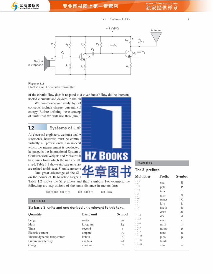
Figure 1.2Electric circuit of a radio transmitter.
TABLE 1.1
Six basic SI units and one derived unit relevant to this text.
Quantity Basic unit SymbolLength meter mMass kilogram kgTime second sElectric current ampere AThermodynamic temperature kelvin KLuminous intensity candela cdCharge coulomb C
TABLE 1.2
The SI prefixes.
Multiplier Prefix Symbol1018 exa E1015 peta P1012 tera T109 giga G106 mega M103 kilo k102 hecto h10 deka da10−1 deci d10−2 centi c10−3 milli m10−6 micro μ10−9 nano n10−12 pico p10−15 femto f10−18 atto a
aLe26409_ch01_002-028.indd 5 9/27/19 1:19 PM
4 Chapter 1 Basic Concepts
1.1 IntroductionElectric circuit theory and electromagnetic theory are the two fundamen-tal theories upon which all branches of electrical engineering are built. Many branches of electrical engineering, such as power, electric ma-chines, control, electronics, communications, and instrumentation, are based on electric circuit theory. Therefore, the basic electric circuit theory course is the most important course for an electrical engineering student, and always an excellent starting point for a beginning student in electri-cal engineering education. Circuit theory is also valuable to students spe-cializing in other branches of the physical sciences because circuits are a good model for the study of energy systems in general, and because of the applied mathematics, physics, and topology involved.
In electrical engineering, we are often interested in communicating or transferring energy from one point to another. To do this requires an interconnection of electrical devices. Such interconnection is referred to as an electric circuit, and each component of the circuit is known as an element.
An electric circuit is an interconnection of electrical elements.
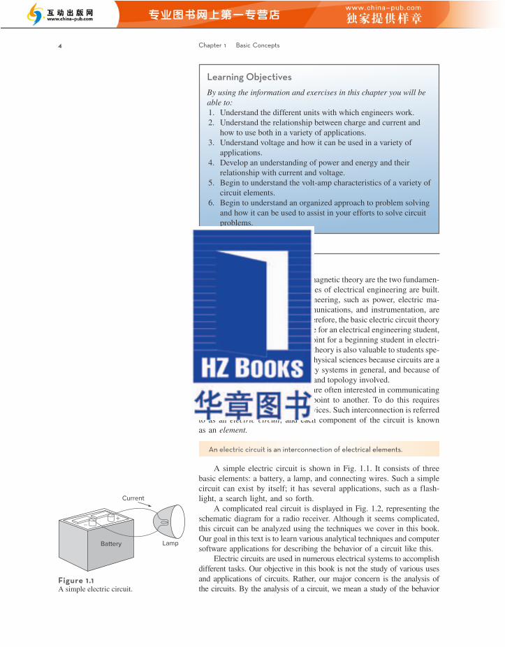
A simple electric circuit is shown in Fig. 1.1. It consists of three basic elements: a battery, a lamp, and connecting wires. Such a simple circuit can exist by itself; it has several applications, such as a flash- light, a search light, and so forth.
A complicated real circuit is displayed in Fig. 1.2, representing the schematic diagram for a radio receiver. Although it seems complicated, this circuit can be analyzed using the techniques we cover in this book. Our goal in this text is to learn various analytical techniques and computer software applications for describing the behavior of a circuit like this.
Electric circuits are used in numerous electrical systems to accomplish different tasks. Our objective in this book is not the study of various uses and applications of circuits. Rather, our major concern is the analysis of the circuits. By the analysis of a circuit, we mean a study of the behavior
Learning ObjectivesBy using the information and exercises in this chapter you will be able to:1. Understand the different units with which engineers work.2. Understand the relationship between charge and current and
how to use both in a variety of applications.3. Understand voltage and how it can be used in a variety of
applications.4. Develop an understanding of power and energy and their
relationship with current and voltage.5. Begin to understand the volt-amp characteristics of a variety of
circuit elements.6. Begin to understand an organized approach to problem solving
and how it can be used to assist in your efforts to solve circuit problems.
+–
Current
LampBattery
Figure 1.1A simple electric circuit.
aLe26409_ch01_002-028.indd 4 9/27/19 1:19 PM
1.2 Systems of Units 5
of the circuit: How does it respond to a given input? How do the intercon-nected elements and devices in the circuit interact?
We commence our study by defining some basic concepts. These concepts include charge, current, voltage, circuit elements, power, and energy. Before defining these concepts, we must first establish a system of units that we will use throughout the text.
1.2 Systems of UnitsAs electrical engineers, we must deal with measurable quantities. Our mea-surements, however, must be communicated in a standard language that virtually all professionals can understand, irrespective of the country in which the measurement is conducted. Such an international measurement language is the International System of Units (SI), adopted by the General Conference on Weights and Measures in 1960. In this system, there are seven base units from which the units of all other physical quantities can be de-rived. Table 1.1 shows six base units and one derived unit (the coulomb) that are related to this text. SI units are commonly used in electrical engineering.
One great advantage of the SI unit is that it uses prefixes based on the power of 10 to relate larger and smaller units to the basic unit. Table 1.2 shows the SI prefixes and their symbols. For example, the following are expressions of the same distance in meters (m):
600,000,000 mm 600,000 m 600 km
L1C4
Antenna
C5Q2
R7
R2 R4 R6
R3 R5
C1
C3
C2
Electretmicrophone
R1
+
–
+ 9 V (DC)
Q1
Figure 1.2Electric circuit of a radio transmitter.
TABLE 1.1
Six basic SI units and one derived unit relevant to this text.
Quantity Basic unit SymbolLength meter mMass kilogram kgTime second sElectric current ampere AThermodynamic temperature kelvin KLuminous intensity candela cdCharge coulomb C
TABLE 1.2
The SI prefixes.
Multiplier Prefix Symbol1018 exa E1015 peta P1012 tera T109 giga G106 mega M103 kilo k102 hecto h10 deka da10−1 deci d10−2 centi c10−3 milli m10−6 micro μ10−9 nano n10−12 pico p10−15 femto f10−18 atto a
aLe26409_ch01_002-028.indd 5 9/27/19 1:19 PM
4 Chapter 1 Basic Concepts
1.1 IntroductionElectric circuit theory and electromagnetic theory are the two fundamen-tal theories upon which all branches of electrical engineering are built. Many branches of electrical engineering, such as power, electric ma-chines, control, electronics, communications, and instrumentation, are based on electric circuit theory. Therefore, the basic electric circuit theory course is the most important course for an electrical engineering student, and always an excellent starting point for a beginning student in electri-cal engineering education. Circuit theory is also valuable to students spe-cializing in other branches of the physical sciences because circuits are a good model for the study of energy systems in general, and because of the applied mathematics, physics, and topology involved.
In electrical engineering, we are often interested in communicating or transferring energy from one point to another. To do this requires an interconnection of electrical devices. Such interconnection is referred to as an electric circuit, and each component of the circuit is known as an element.
An electric circuit is an interconnection of electrical elements.
A simple electric circuit is shown in Fig. 1.1. It consists of three basic elements: a battery, a lamp, and connecting wires. Such a simple circuit can exist by itself; it has several applications, such as a flash- light, a search light, and so forth.
A complicated real circuit is displayed in Fig. 1.2, representing the schematic diagram for a radio receiver. Although it seems complicated, this circuit can be analyzed using the techniques we cover in this book. Our goal in this text is to learn various analytical techniques and computer software applications for describing the behavior of a circuit like this.
Electric circuits are used in numerous electrical systems to accomplish different tasks. Our objective in this book is not the study of various uses and applications of circuits. Rather, our major concern is the analysis of the circuits. By the analysis of a circuit, we mean a study of the behavior
Learning ObjectivesBy using the information and exercises in this chapter you will be able to:1. Understand the different units with which engineers work.2. Understand the relationship between charge and current and
how to use both in a variety of applications.3. Understand voltage and how it can be used in a variety of
applications.4. Develop an understanding of power and energy and their
relationship with current and voltage.5. Begin to understand the volt-amp characteristics of a variety of
circuit elements.6. Begin to understand an organized approach to problem solving
and how it can be used to assist in your efforts to solve circuit problems.
+–
Current
LampBattery
Figure 1.1A simple electric circuit.
aLe26409_ch01_002-028.indd 4 9/27/19 1:19 PM
1.3 Charge and Current 7
where current is measured in amperes (A), and1 ampere = 1 coulomb/second
The charge transferred between time t0 and t is obtained by integrating both sides of Eq. (1.1). We obtain
Q = Δ ∫t0
t
i dt (1.2)
The way we define current as i in Eq. (1.1) suggests that current need not be a constant-valued function. As many of the examples and problems in this chapter and subsequent chapters suggest, there can be several types of current; that is, charge can vary with time in several ways.
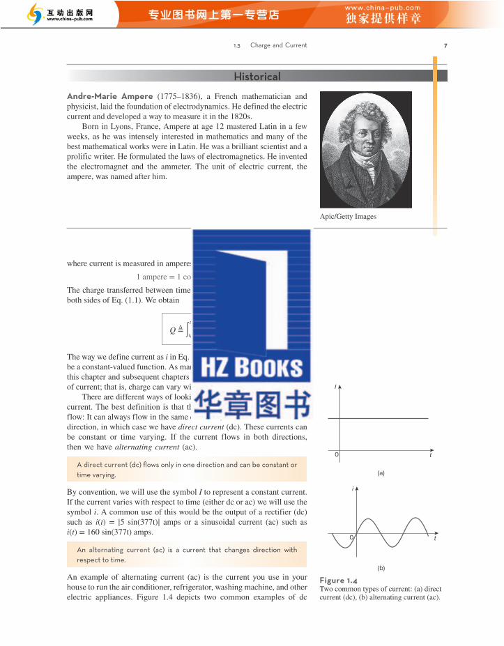
There are different ways of looking at direct current and alternating current. The best definition is that there are two ways that current can flow: It can always flow in the same direction, where it does not reverse direction, in which case we have direct current (dc). These currents can be constant or time varying. If the current flows in both directions, then we have alternating current (ac).
A direct current (dc) flows only in one direction and can be constant or time varying.
By convention, we will use the symbol I to represent a constant current. If the current varies with respect to time (either dc or ac) we will use the symbol i. A common use of this would be the output of a rectifier (dc) such as i(t) = ∣5 sin(377t)∣ amps or a sinusoidal current (ac) such as i(t) = 160 sin(377t) amps.
An alternating current (ac) is a current that changes direction with respect to time.
An example of alternating current (ac) is the current you use in your house to run the air conditioner, refrigerator, washing machine, and other electric appliances. Figure 1.4 depicts two common examples of dc
Andre-Marie Ampere (1775–1836), a French mathematician and physicist, laid the foundation of electrodynamics. He defined the electric current and developed a way to measure it in the 1820s.
Born in Lyons, France, Ampere at age 12 mastered Latin in a few weeks, as he was intensely interested in mathematics and many of the best mathematical works were in Latin. He was a brilliant scientist and a prolific writer. He formulated the laws of electromagnetics. He in vented the electromagnet and the ammeter. The unit of electric current, the ampere, was named after him.
Apic/Getty Images
Historical
I
0 t
(a)
(b)
i
t0
Figure 1.4Two common types of current: (a) direct current (dc), (b) alternating current (ac).
aLe26409_ch01_002-028.indd 7 9/27/19 1:19 PM
6 Chapter 1 Basic Concepts
1.3 Charge and CurrentThe concept of electric charge is the underlying principle for explaining all electrical phenomena. Also, the most basic quantity in an electric circuit is the electric charge. We all experience the effect of electric charge when we try to remove our wool sweater and have it stick to our body or walk across a carpet and receive a shock.
Charge is an electrical property of the atomic particles of which matter consists, measured in coulombs (C).
We know from elementary physics that all matter is made of fundamental building blocks known as atoms and that each atom consists of electrons, protons, and neutrons. We also know that the charge e on an electron is negative and equal in magnitude to 1.602 × 10⁻¹⁹ C, while a proton carries a positive charge of the same magnitude as the electron. The presence of equal numbers of protons and electrons leaves an atom neutrally charged.
The following points should be noted about electric charge:
1. The coulomb is a large unit for charges. In 1 C of charge, there are 1∕(1.602 × 10⁻¹⁹) = 6.24 × 10¹⁸ electrons. Thus realistic or labora-tory values of charges are on the order of pC, nC, or μC.1
2. According to experimental observations, the only charges that occur in nature are integral multiples of the electronic charge e = −1.602 × 10⁻¹⁹ C.
3. The law of conservation of charge states that charge can neither be created nor destroyed, only transferred. Thus, the algebraic sum of the electric charges in a system does not change.
We now consider the flow of electric charges. A unique feature of electric charge or electricity is the fact that it is mobile; that is, it can be transferred from one place to another, where it can be converted to another form of energy.
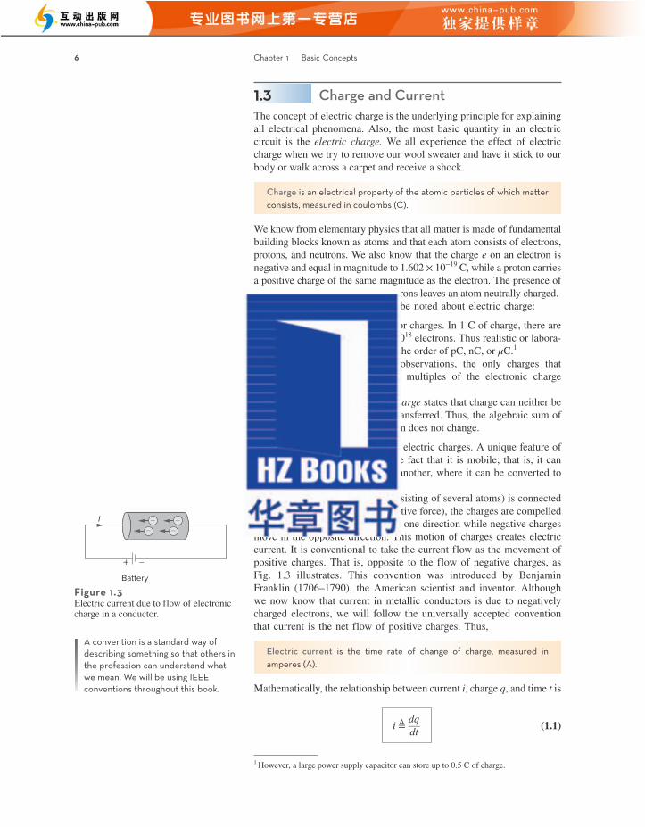
When a conducting wire (consisting of several atoms) is connected to a battery (a source of electromotive force), the charges are compelled to move; positive charges move in one direction while negative charges move in the opposite direction. This motion of charges creates electric current. It is conventional to take the current flow as the movement of positive charges. That is, opposite to the flow of negative charges, as Fig. 1.3 illustrates. This convention was introduced by Benjamin Franklin (1706–1790), the American scientist and inventor. Although we now know that current in metallic conductors is due to negatively charged electrons, we will follow the universally accepted convention that current is the net flow of positive charges. Thus,
Electric current is the time rate of change of charge, measured in amperes (A).
Mathematically, the relationship between current i, charge q, and time t is
i = Δ dq ___
dt (1.1)
A convention is a standard way of describing something so that others in the profession can understand what we mean. We will be using IEEE conventions throughout this book.
Battery
I–
+ –
–––
Figure 1.3Electric current due to flow of electronic charge in a conductor.
1 However, a large power supply capacitor can store up to 0.5 C of charge.
aLe26409_ch01_002-028.indd 6 9/27/19 1:19 PM
1.3 Charge and Current 7
where current is measured in amperes (A), and1 ampere = 1 coulomb/second
The charge transferred between time t0 and t is obtained by integrating both sides of Eq. (1.1). We obtain
Q = Δ ∫t0
t
i dt (1.2)
The way we define current as i in Eq. (1.1) suggests that current need not be a constant-valued function. As many of the examples and problems in this chapter and subsequent chapters suggest, there can be several types of current; that is, charge can vary with time in several ways.
There are different ways of looking at direct current and alternating current. The best definition is that there are two ways that current can flow: It can always flow in the same direction, where it does not reverse direction, in which case we have direct current (dc). These currents can be constant or time varying. If the current flows in both directions, then we have alternating current (ac).
A direct current (dc) flows only in one direction and can be constant or time varying.
By convention, we will use the symbol I to represent a constant current. If the current varies with respect to time (either dc or ac) we will use the symbol i. A common use of this would be the output of a rectifier (dc) such as i(t) = ∣5 sin(377t)∣ amps or a sinusoidal current (ac) such as i(t) = 160 sin(377t) amps.
An alternating current (ac) is a current that changes direction with respect to time.
An example of alternating current (ac) is the current you use in your house to run the air conditioner, refrigerator, washing machine, and other electric appliances. Figure 1.4 depicts two common examples of dc
Andre-Marie Ampere (1775–1836), a French mathematician and physicist, laid the foundation of electrodynamics. He defined the electric current and developed a way to measure it in the 1820s.
Born in Lyons, France, Ampere at age 12 mastered Latin in a few weeks, as he was intensely interested in mathematics and many of the best mathematical works were in Latin. He was a brilliant scientist and a prolific writer. He formulated the laws of electromagnetics. He in vented the electromagnet and the ammeter. The unit of electric current, the ampere, was named after him.
Apic/Getty Images
Historical
I
0 t
(a)
(b)
i
t0
Figure 1.4Two common types of current: (a) direct current (dc), (b) alternating current (ac).
aLe26409_ch01_002-028.indd 7 9/27/19 1:19 PM
6 Chapter 1 Basic Concepts
1.3 Charge and CurrentThe concept of electric charge is the underlying principle for explaining all electrical phenomena. Also, the most basic quantity in an electric circuit is the electric charge. We all experience the effect of electric charge when we try to remove our wool sweater and have it stick to our body or walk across a carpet and receive a shock.
Charge is an electrical property of the atomic particles of which matter consists, measured in coulombs (C).
We know from elementary physics that all matter is made of fundamental building blocks known as atoms and that each atom consists of electrons, protons, and neutrons. We also know that the charge e on an electron is negative and equal in magnitude to 1.602 × 10⁻¹⁹ C, while a proton carries a positive charge of the same magnitude as the electron. The presence of equal numbers of protons and electrons leaves an atom neutrally charged.
The following points should be noted about electric charge:
1. The coulomb is a large unit for charges. In 1 C of charge, there are 1∕(1.602 × 10⁻¹⁹) = 6.24 × 10¹⁸ electrons. Thus realistic or labora-tory values of charges are on the order of pC, nC, or μC.1
2. According to experimental observations, the only charges that occur in nature are integral multiples of the electronic charge e = −1.602 × 10⁻¹⁹ C.
3. The law of conservation of charge states that charge can neither be created nor destroyed, only transferred. Thus, the algebraic sum of the electric charges in a system does not change.
We now consider the flow of electric charges. A unique feature of electric charge or electricity is the fact that it is mobile; that is, it can be transferred from one place to another, where it can be converted to another form of energy.
When a conducting wire (consisting of several atoms) is connected to a battery (a source of electromotive force), the charges are compelled to move; positive charges move in one direction while negative charges move in the opposite direction. This motion of charges creates electric current. It is conventional to take the current flow as the movement of positive charges. That is, opposite to the flow of negative charges, as Fig. 1.3 illustrates. This convention was introduced by Benjamin Franklin (1706–1790), the American scientist and inventor. Although we now know that current in metallic conductors is due to negatively charged electrons, we will follow the universally accepted convention that current is the net flow of positive charges. Thus,
Electric current is the time rate of change of charge, measured in amperes (A).
Mathematically, the relationship between current i, charge q, and time t is
i = Δ dq ___
dt (1.1)
A convention is a standard way of describing something so that others in the profession can understand what we mean. We will be using IEEE conventions throughout this book.
Battery
I–
+ –
–––
Figure 1.3Electric current due to flow of electronic charge in a conductor.
1 However, a large power supply capacitor can store up to 0.5 C of charge.
aLe26409_ch01_002-028.indd 6 9/27/19 1:19 PM
1.4 Voltage 9
The current flowing through an element is
i = 8 A,
0 < t < 1
8t2 A,
t > 1
Calculate the charge entering the element from t = 0 to t = 2 s.
Answer: 26.67 C.
Practice Problem 1.3
1.4 VoltageAs explained briefly in the previous section, to move the electron in a conductor in a particular direction requires some work or energy transfer. This work is performed by an external electromotive force (emf), typi-cally represented by the battery in Fig. 1.3. This emf is also known as voltage or potential difference. The voltage vab between two points a and b in an electric circuit is the energy (or work) needed to move a unit charge from b to a; mathematically,
vab = Δ dw ___ dq
(1.3)
where w is energy in joules (J) and q is charge in coulombs (C). The volt-age vab or simply v is measured in volts (V), named in honor of the Italian physicist Alessandro Antonio Volta (1745–1827), who invented the first voltaic battery. From Eq. (1.3), it is evident that
1 volt = 1 joule/coulomb = 1 newton-meter/coulomb
Thus,
Voltage (or potential difference) is the energy required to move a unit charge from a reference point (−) to another point (+), measured in volts (V).
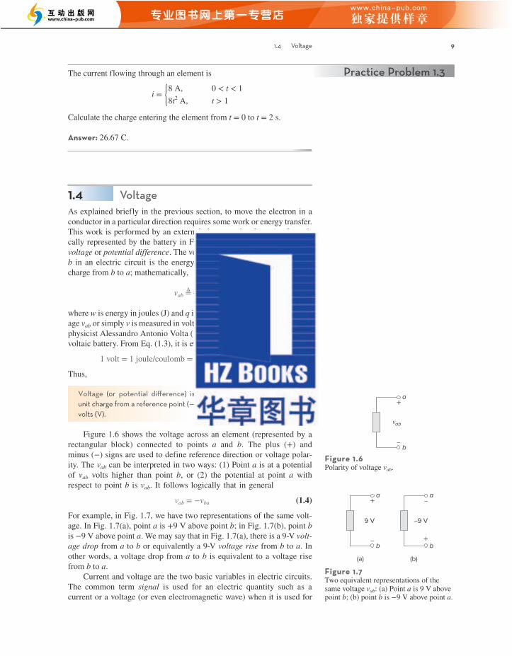
Figure 1.6 shows the voltage across an element (represented by a rectangular block) connected to points a and b. The plus (+) and minus (−) signs are used to define reference direction or voltage polar-ity. The vab can be interpreted in two ways: (1) Point a is at a potential of vab volts higher than point b, or (2) the potential at point a with respect to point b is vab. It follows logically that in general
vab = −vba (1.4)
For example, in Fig. 1.7, we have two representations of the same volt-age. In Fig. 1.7(a), point a is +9 V above point b; in Fig. 1.7(b), point b is −9 V above point a. We may say that in Fig. 1.7(a), there is a 9-V volt-age drop from a to b or equivalently a 9-V voltage rise from b to a. In other words, a voltage drop from a to b is equivalent to a voltage rise from b to a.
Current and voltage are the two basic variables in electric circuits. The common term signal is used for an electric quantity such as a current or a voltage (or even electromagnetic wave) when it is used for
a
b
vab
+
–
Figure 1.6Polarity of voltage vab.
9 V
(a)
a
b
+
–
–9 V
(b)
a
b+
–
Figure 1.7Two equivalent representations of the same voltage vab: (a) Point a is 9 V above point b; (b) point b is −9 V above point a.
aLe26409_ch01_002-028.indd 9 9/27/19 1:19 PM
8 Chapter 1 Basic Concepts
(coming from a battery) and ac (coming from your home outlets). We will consider other types later in the book.
Once we define current as the movement of charge, we expect current to have an associated direction of flow. As mentioned earlier, the direction of current flow is conventionally taken as the direction of positive charge movement. Based on this convention, a current of 5 A may be represented positively or negatively as shown in Fig. 1.5. In other words, a negative current of −5 A flowing in one direction as shown in Fig. 1.5(b) is the same as a current of +5 A flowing in the opposite direction.
5 A
(a)
–5 A
(b)
Figure 1.5Conventional current flow: (a) positive current flow, (b) negative current flow.
Example 1.1 How much charge is represented by 4,600 electrons?
Solution:Each electron has −1.602 × 10⁻¹⁹ C. Hence 4,600 electrons will have −1.602 × 10⁻¹⁹ C/electron × 4,600 electrons = −7.369 × 10⁻¹⁶ C
Example 1.2 The total charge entering a terminal is given by q = 5t sin 4πt mC. Calculate the current at t = 0.5 s.
Solution:
i = dq ___
dt = d __
dt (5t sin 4πt) mC/s = (5 sin 4πt + 20πt cos 4πt) mA
At t = 0.5,
i = 5 sin 2π + 10π cos 2π = 0 + 10π = 31.42 mA
Calculate the amount of charge represented by 10 billion protons.
Answer: 1.6021 × 10⁻⁹ C.
Practice Problem 1.1
If in Example 1.2, q = (20 – 15t – 10e−3t ) mC, find the current at t = 1.0 s.
Answer: −13.506 mA.
Practice Problem 1.2
Example 1.3 Determine the total charge entering a terminal between t = 1 s and t = 2 s if the current passing the terminal is i = (3t2 − t) A.
Solution:
Q = ∫t=1
2 i dt = ∫1
2 (3t2 − t) dt
= ( t3 − t2 __ 2 ) ∣ 1
2 = (8 − 2) − ( 1 − 1 __ 2 ) = 5.5 C
aLe26409_ch01_002-028.indd 8 9/27/19 1:19 PM
1.4 Voltage 9
The current flowing through an element is
i = 8 A,
0 < t < 1
8t2 A,
t > 1
Calculate the charge entering the element from t = 0 to t = 2 s.
Answer: 26.67 C.
Practice Problem 1.3
1.4 VoltageAs explained briefly in the previous section, to move the electron in a conductor in a particular direction requires some work or energy transfer. This work is performed by an external electromotive force (emf), typi-cally represented by the battery in Fig. 1.3. This emf is also known as voltage or potential difference. The voltage vab between two points a and b in an electric circuit is the energy (or work) needed to move a unit charge from b to a; mathematically,
vab = Δ dw ___ dq
(1.3)
where w is energy in joules (J) and q is charge in coulombs (C). The volt-age vab or simply v is measured in volts (V), named in honor of the Italian physicist Alessandro Antonio Volta (1745–1827), who invented the first voltaic battery. From Eq. (1.3), it is evident that
1 volt = 1 joule/coulomb = 1 newton-meter/coulomb
Thus,
Voltage (or potential difference) is the energy required to move a unit charge from a reference point (−) to another point (+), measured in volts (V).
Figure 1.6 shows the voltage across an element (represented by a rectangular block) connected to points a and b. The plus (+) and minus (−) signs are used to define reference direction or voltage polar-ity. The vab can be interpreted in two ways: (1) Point a is at a potential of vab volts higher than point b, or (2) the potential at point a with respect to point b is vab. It follows logically that in general
vab = −vba (1.4)
For example, in Fig. 1.7, we have two representations of the same volt-age. In Fig. 1.7(a), point a is +9 V above point b; in Fig. 1.7(b), point b is −9 V above point a. We may say that in Fig. 1.7(a), there is a 9-V volt-age drop from a to b or equivalently a 9-V voltage rise from b to a. In other words, a voltage drop from a to b is equivalent to a voltage rise from b to a.
Current and voltage are the two basic variables in electric circuits. The common term signal is used for an electric quantity such as a current or a voltage (or even electromagnetic wave) when it is used for
a
b
vab
+
–
Figure 1.6Polarity of voltage vab.
9 V
(a)
a
b
+
–
–9 V
(b)
a
b+
–
Figure 1.7Two equivalent representations of the same voltage vab: (a) Point a is 9 V above point b; (b) point b is −9 V above point a.
aLe26409_ch01_002-028.indd 9 9/27/19 1:19 PM
8 Chapter 1 Basic Concepts
(coming from a battery) and ac (coming from your home outlets). We will consider other types later in the book.
Once we define current as the movement of charge, we expect current to have an associated direction of flow. As mentioned earlier, the direction of current flow is conventionally taken as the direction of positive charge movement. Based on this convention, a current of 5 A may be represented positively or negatively as shown in Fig. 1.5. In other words, a negative current of −5 A flowing in one direction as shown in Fig. 1.5(b) is the same as a current of +5 A flowing in the opposite direction.
5 A
(a)
–5 A
(b)
Figure 1.5Conventional current flow: (a) positive current flow, (b) negative current flow.
Example 1.1 How much charge is represented by 4,600 electrons?
Solution:Each electron has −1.602 × 10⁻¹⁹ C. Hence 4,600 electrons will have −1.602 × 10⁻¹⁹ C/electron × 4,600 electrons = −7.369 × 10⁻¹⁶ C
Example 1.2 The total charge entering a terminal is given by q = 5t sin 4πt mC. Calculate the current at t = 0.5 s.
Solution:
i = dq ___
dt = d __
dt (5t sin 4πt) mC/s = (5 sin 4πt + 20πt cos 4πt) mA
At t = 0.5,
i = 5 sin 2π + 10π cos 2π = 0 + 10π = 31.42 mA
Calculate the amount of charge represented by 10 billion protons.
Answer: 1.6021 × 10⁻⁹ C.
Practice Problem 1.1
If in Example 1.2, q = (20 – 15t – 10e−3t ) mC, find the current at t = 1.0 s.
Answer: −13.506 mA.
Practice Problem 1.2
Example 1.3 Determine the total charge entering a terminal between t = 1 s and t = 2 s if the current passing the terminal is i = (3t2 − t) A.
Solution:
Q = ∫t=1
2 i dt = ∫1
2 (3t2 − t) dt
= ( t3 − t2 __ 2 ) ∣ 1
2 = (8 − 2) − ( 1 − 1 __ 2 ) = 5.5 C
aLe26409_ch01_002-028.indd 8 9/27/19 1:19 PM
1.5 Power and Energy 11
where p is power in watts (W), w is energy in joules (J), and t is time in seconds (s). From Eqs. (1.1), (1.3), and (1.5), it follows that
p = dw ___ dt
= dw ___ dq
⋅ dq __
dt = vi (1.6)
or
p = vi (1.7)
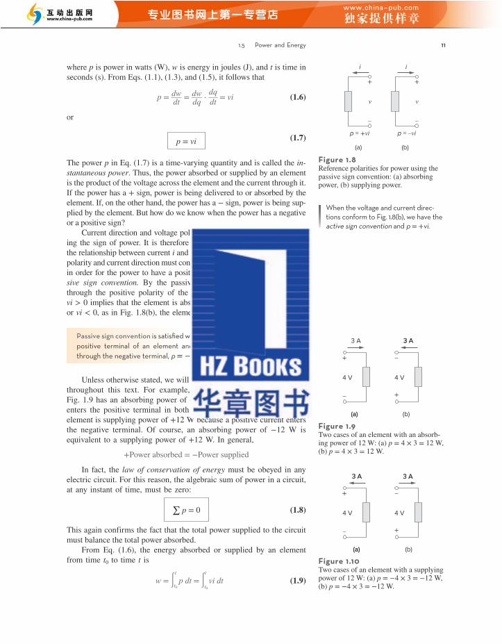
The power p in Eq. (1.7) is a time-varying quantity and is called the in-stantaneous power. Thus, the power absorbed or supplied by an element is the product of the voltage across the element and the current through it. If the power has a + sign, power is being delivered to or absorbed by the element. If, on the other hand, the power has a − sign, power is being sup-plied by the element. But how do we know when the power has a negative or a positive sign?
Current direction and voltage polarity play a major role in determin-ing the sign of power. It is therefore important that we pay attention to the relationship between current i and voltage v in Fig. 1.8(a). The voltage polarity and current direction must conform with those shown in Fig. 1.8(a) in order for the power to have a positive sign. This is known as the pas-sive sign convention. By the passive sign convention, current enters through the positive polarity of the voltage. In this case, p = +vi or vi > 0 implies that the element is absorbing power. However, if p = −vi or vi < 0, as in Fig. 1.8(b), the element is releasing or supplying power.
Passive sign convention is satisfied when the current enters through the positive terminal of an element and p = +vi. If the current enters through the negative terminal, p = −vi.
Unless otherwise stated, we will follow the passive sign convention throughout this text. For example, the element in both circuits of Fig. 1.9 has an absorbing power of +12 W because a positive current enters the positive terminal in both cases. In Fig. 1.10, however, the element is supplying power of +12 W because a positive current enters the negative terminal. Of course, an absorbing power of −12 W is equivalent to a supplying power of +12 W. In general,
+Power absorbed = −Power supplied
In fact, the law of conservation of energy must be obeyed in any electric circuit. For this reason, the algebraic sum of power in a circuit, at any instant of time, must be zero:
∑ p = 0 (1.8)
This again confirms the fact that the total power supplied to the circuit must balance the total power absorbed.
From Eq. (1.6), the energy absorbed or supplied by an element from time t0 to time t is
w = ∫t0
t
p dt = ∫t0
t vi dt (1.9)
p = +vi
(a)
v
+
–
p = –vi
(b)
v
+
–
ii
Figure 1.8Reference polarities for power using the passive sign convention: (a) absorbing power, (b) supplying power.
(a)
4 V
3 A
(a)
+
–
3 A
4 V
3 A
(b)
+
–
Figure 1.9Two cases of an element with an absorb-ing power of 12 W: (a) p = 4 × 3 = 12 W, (b) p = 4 × 3 = 12 W.
3 A
(a)
4 V
3 A
(a)
+
–
3 A
4 V
3 A
(b)
+
–
Figure 1.10Two cases of an element with a supplying power of 12 W: (a) p = −4 × 3 = −12 W, (b) p = −4 × 3 = −12 W.
When the voltage and current direc-tions conform to Fig. 1.8(b), we have the active sign convention and p = +vi.
aLe26409_ch01_002-028.indd 11 9/27/19 1:20 PM
10 Chapter 1 Basic Concepts
conveying information. Engineers prefer to call such variables signals rather than mathematical functions of time because of their importance in communications and other disciplines. Like electric current, a con-stant voltage is called a dc voltage and is represented by V, whereas a sinusoidally time-varying voltage is called an ac voltage and is repre-sented by v. A dc voltage is commonly produced by a battery; ac volt-age is produced by an electric generator.
1.5 Power and EnergyAlthough current and voltage are the two basic variables in an electric circuit, they are not sufficient by themselves. For practical purposes, we need to know how much power an electric device can handle. We all know from experience that a 100-watt bulb gives more light than a 60-watt bulb. We also know that when we pay our bills to the electric utility companies, we are paying for the electric energy consumed over a certain period of time. Thus, power and energy calculations are impor-tant in circuit analysis.
To relate power and energy to voltage and current, we recall from physics that:
Power is the time rate of expending or absorbing energy, measured in watts (W).
We write this relationship as
p = Δ dw ___ dt
(1.5)
Keep in mind that electric current is always through an element and that electric voltage is always across the element or between two points.
Historical
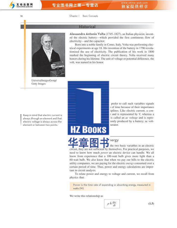
Alessandro Antonio Volta (1745–1827), an Italian physicist, invent-ed the electric battery—which provided the first continuous flow of electricity—and the capacitor.
Born into a noble family in Como, Italy, Volta was performing elec-trical experiments at age 18. His invention of the battery in 1796 revolu-tionized the use of electricity. The publication of his work in 1800 marked the beginning of electric circuit theory. Volta received many honors during his lifetime. The unit of voltage or potential difference, the volt, was named in his honor.
UniversalImagesGroup/ Getty Images
aLe26409_ch01_002-028.indd 10 9/27/19 1:20 PM
1.5 Power and Energy 11
where p is power in watts (W), w is energy in joules (J), and t is time in seconds (s). From Eqs. (1.1), (1.3), and (1.5), it follows that
p = dw ___ dt
= dw ___ dq
⋅ dq __
dt = vi (1.6)
or
p = vi (1.7)
The power p in Eq. (1.7) is a time-varying quantity and is called the in-stantaneous power. Thus, the power absorbed or supplied by an element is the product of the voltage across the element and the current through it. If the power has a + sign, power is being delivered to or absorbed by the element. If, on the other hand, the power has a − sign, power is being sup-plied by the element. But how do we know when the power has a negative or a positive sign?
Current direction and voltage polarity play a major role in determin-ing the sign of power. It is therefore important that we pay attention to the relationship between current i and voltage v in Fig. 1.8(a). The voltage polarity and current direction must conform with those shown in Fig. 1.8(a) in order for the power to have a positive sign. This is known as the pas-sive sign convention. By the passive sign convention, current enters through the positive polarity of the voltage. In this case, p = +vi or vi > 0 implies that the element is absorbing power. However, if p = −vi or vi < 0, as in Fig. 1.8(b), the element is releasing or supplying power.
Passive sign convention is satisfied when the current enters through the positive terminal of an element and p = +vi. If the current enters through the negative terminal, p = −vi.
Unless otherwise stated, we will follow the passive sign convention throughout this text. For example, the element in both circuits of Fig. 1.9 has an absorbing power of +12 W because a positive current enters the positive terminal in both cases. In Fig. 1.10, however, the element is supplying power of +12 W because a positive current enters the negative terminal. Of course, an absorbing power of −12 W is equivalent to a supplying power of +12 W. In general,
+Power absorbed = −Power supplied
In fact, the law of conservation of energy must be obeyed in any electric circuit. For this reason, the algebraic sum of power in a circuit, at any instant of time, must be zero:
∑ p = 0 (1.8)
This again confirms the fact that the total power supplied to the circuit must balance the total power absorbed.
From Eq. (1.6), the energy absorbed or supplied by an element from time t0 to time t is
w = ∫t0
t
p dt = ∫t0
t vi dt (1.9)
p = +vi
(a)
v
+
–
p = –vi
(b)
v
+
–
ii
Figure 1.8Reference polarities for power using the passive sign convention: (a) absorbing power, (b) supplying power.
(a)
4 V
3 A
(a)
+
–
3 A
4 V
3 A
(b)
+
–
Figure 1.9Two cases of an element with an absorb-ing power of 12 W: (a) p = 4 × 3 = 12 W, (b) p = 4 × 3 = 12 W.
3 A
(a)
4 V
3 A
(a)
+
–
3 A
4 V
3 A
(b)
+
–
Figure 1.10Two cases of an element with a supplying power of 12 W: (a) p = −4 × 3 = −12 W, (b) p = −4 × 3 = −12 W.
When the voltage and current direc-tions conform to Fig. 1.8(b), we have the active sign convention and p = +vi.
aLe26409_ch01_002-028.indd 11 9/27/19 1:20 PM
10 Chapter 1 Basic Concepts
conveying information. Engineers prefer to call such variables signals rather than mathematical functions of time because of their importance in communications and other disciplines. Like electric current, a con-stant voltage is called a dc voltage and is represented by V, whereas a sinusoidally time-varying voltage is called an ac voltage and is repre-sented by v. A dc voltage is commonly produced by a battery; ac volt-age is produced by an electric generator.
1.5 Power and EnergyAlthough current and voltage are the two basic variables in an electric circuit, they are not sufficient by themselves. For practical purposes, we need to know how much power an electric device can handle. We all know from experience that a 100-watt bulb gives more light than a 60-watt bulb. We also know that when we pay our bills to the electric utility companies, we are paying for the electric energy consumed over a certain period of time. Thus, power and energy calculations are impor-tant in circuit analysis.
To relate power and energy to voltage and current, we recall from physics that:
Power is the time rate of expending or absorbing energy, measured in watts (W).
We write this relationship as
p = Δ dw ___ dt
(1.5)
Keep in mind that electric current is always through an element and that electric voltage is always across the element or between two points.
Historical
Alessandro Antonio Volta (1745–1827), an Italian physicist, invent-ed the electric battery—which provided the first continuous flow of electricity—and the capacitor.
Born into a noble family in Como, Italy, Volta was performing elec-trical experiments at age 18. His invention of the battery in 1796 revolu-tionized the use of electricity. The publication of his work in 1800 marked the beginning of electric circuit theory. Volta received many honors during his lifetime. The unit of voltage or potential difference, the volt, was named in his honor.
UniversalImagesGroup/ Getty Images
aLe26409_ch01_002-028.indd 10 9/27/19 1:20 PM
1.5 Power and Energy 13
Find the power delivered to the element in Example 1.5 at t = 5 ms if the current remains the same but the voltage is: (a) v = 6i V,
(b) v = (6 + 10 ∫0
t
i dt) V.
Answer: (a) 51.82 W, (b) 18.264 watts.
Practice Problem 1.5
Source: IEEE History Center
Historical
1884 Exhibition In the United States, nothing promoted the future of electricity like the 1884 International Electrical Exhibition. Just imagine a world without electricity, a world illuminated by candles and gaslights, a world where the most common transportation was by walking and rid-ing on horseback or by horse-drawn carriage. Into this world an exhibi-tion was created that highlighted Thomas Edison and reflected his high-ly developed ability to promote his inventions and products. His exhibit featured spectacular lighting displays powered by an impressive 100-kW “Jumbo” generator.
Edward Weston’s dynamos and lamps were featured in the United States Electric Lighting Company’s display. Weston’s well known col-lection of scientific instruments was also shown.
Other prominent exhibitors included Frank Sprague, Elihu Thompson, and the Brush Electric Company of Cleveland. The American Institute of Electrical Engineers (AIEE) held its first technical meeting on October 7–8 at the Franklin Institute during the exhibit. AIEE merged with the Institute of Radio Engineers (IRE) in 1964 to form the Institute of Electrical and Electronics Engineers (IEEE).
aLe26409_ch01_002-028.indd 13 9/27/19 1:20 PM
12 Chapter 1 Basic Concepts
Energy is the capacity to do work, measured in joules (J).
The electric power utility companies measure energy in watt-hours (Wh), where
1 Wh = 3,600 J
Example 1.4 An energy source forces a constant current of 2 A for 10 s to flow through a light bulb. If 2.3 kJ is given off in the form of light and heat energy, calculate the voltage drop across the bulb.
Solution:The total charge is
∆q = i ∆t = 2 × 10 = 20 C
The voltage drop is
v = ∆w ___ ∆q = 2.3 × 10³
_______ 20 = 115 V
Example 1.5 Find the power delivered to an element at t = 3 ms if the current entering its positive terminal is
i = 5 cos 60π t A
and the voltage is: (a) v = 3i, (b) v = 3 di∕dt.
Solution:(a) The voltage is v = 3i = 15 cos 60π t; hence, the power is
p = vi = 75 cos2 60π t WAt t = 3 ms,
p = 75 cos2 (60π × 3 × 10−3) = 75 cos2 0.18π = 53.48 W
(b) We find the voltage and the power as
v = 3 di __ dt
= 3(−60π)5 sin 60π t = −900π sin 60π t V
p = vi = −4500π sin 60π t cos 60π t WAt t = 3 ms,
p = −4500π sin 0.18π cos 0.18π W
= −14137.167 sin 32.4° cos 32.4° = −6.396 kW
To move charge q from point b to point a requires 100 J. Find the voltage drop vab (the voltage at a positive with respect to b) if: (a) q = 5 C, (b) q = −10 C.
Answer: (a) 20 V, (b) −10 V.
Practice Problem 1.4
aLe26409_ch01_002-028.indd 12 9/27/19 1:20 PM
1.6 Circuit Elements 15
is necessary to maintain the designated current. The symbol for an inde-pendent current source is displayed in Fig. 1.12, where the arrow indi-cates the direction of current i.
An ideal dependent (or controlled) source is an active element in which the source quantity is controlled by another voltage or current.
Dependent sources are usually designated by diamond-shaped symbols, as shown in Fig. 1.13. Since the control of the dependent source is achieved by a voltage or current of some other element in the circuit, and the source can be voltage or current, it follows that there are four possible types of dependent sources, namely:
1. A voltage-controlled voltage source (VCVS).2. A current-controlled voltage source (CCVS).3. A voltage-controlled current source (VCCS).4. A current-controlled current source (CCCS).
Dependent sources are useful in modeling elements such as transistors, operational amplifiers, and integrated circuits. An example of a current-controlled voltage source is shown on the right-hand side of Fig. 1.14, where the voltage 10i of the voltage source depends on the current i through element C. Students might be surprised that the value of the de-pendent voltage source is 10i V (and not 10i A) because it is a voltage source. The key idea to keep in mind is that a voltage source comes with polarities (+ −) in its symbol, while a current source comes with an ar-row, irrespective of what it depends on.
It should be noted that an ideal voltage source (dependent or independent) will produce any current required to ensure that the ter-minal voltage is as stated, whereas an ideal current source will pro-duce the necessary voltage to ensure the stated current flow. Thus, an ideal source could in theory supply an infinite amount of energy. It should also be noted that not only do sources supply power to a cir-cuit, they can absorb power from a circuit too. For a voltage source, we know the voltage but not the current supplied or drawn by it. By the same token, we know the current supplied by a current source but not the voltage across it.
i
Figure 1.12Symbol for independent current source.
(a) (b)
v +– i
Figure 1.13Symbols for: (a) dependent voltage source, (b) dependent current source.
i
A B
C 10i5 V+–
+
−
Figure 1.14The source on the right-hand side is a current-controlled voltage source.
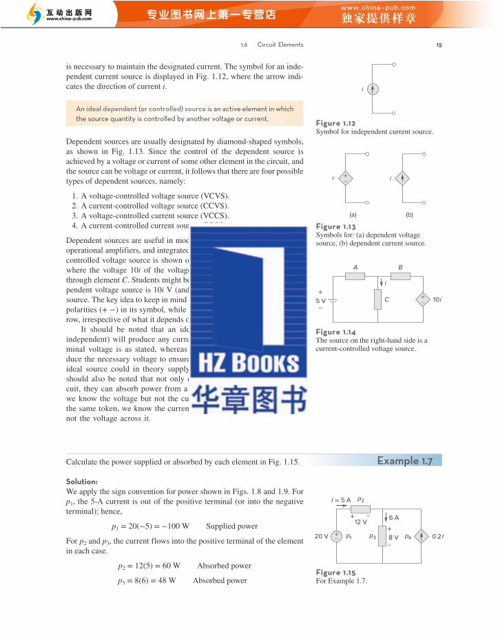
Calculate the power supplied or absorbed by each element in Fig. 1.15.
Solution:We apply the sign convention for power shown in Figs. 1.8 and 1.9. For p1, the 5-A current is out of the positive terminal (or into the negative terminal); hence,
p1 = 20(−5) = −100 W Supplied power
For p2 and p3, the current flows into the positive terminal of the element in each case.
p2 = 12(5) = 60 W Absorbed power
p3 = 8(6) = 48 W Absorbed power
p2
p3
I = 5 A
20 V
6 A
8 V 0.2 I
12 V
+–+
–
+ –
p1 p4
Figure 1.15For Example 1.7.
Example 1.7
aLe26409_ch01_002-028.indd 15 9/27/19 1:20 PM
14 Chapter 1 Basic Concepts
1.6 Circuit ElementsAs we discussed in Section 1.1, an element is the basic building block of a circuit. An electric circuit is simply an interconnection of the elements. Circuit analysis is the process of determining voltages across (or the cur-rents through) the elements of the circuit.
There are two types of elements found in electric circuits: pas-sive elements and active elements. An active element is capable of generating energy while a passive element is not. Examples of pas-sive elements are resistors, capacitors, and inductors. Typical active elements include generators, batteries, and operational amplifiers. Our aim in this section is to gain familiarity with some important active elements.
The most important active elements are voltage or current sources that generally deliver power to the circuit connected to them. There are two kinds of sources: independent and dependent sources.
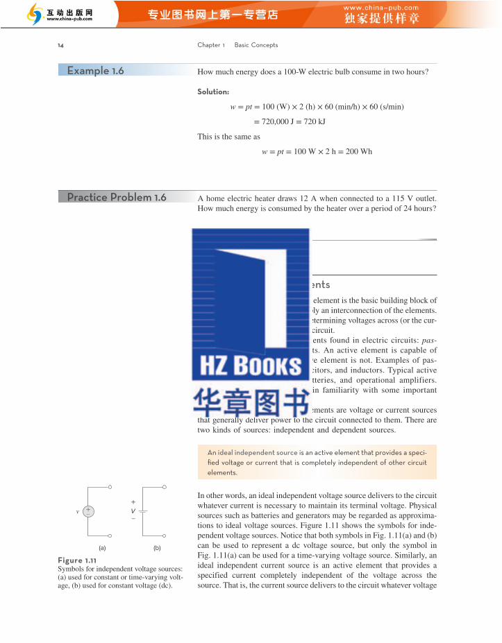
An ideal independent source is an active element that provides a speci-fied voltage or current that is completely independent of other circuit elements.
In other words, an ideal independent voltage source delivers to the circuit whatever current is necessary to maintain its terminal voltage. Physical sources such as batteries and generators may be regarded as approxima-tions to ideal voltage sources. Figure 1.11 shows the symbols for inde-pendent voltage sources. Notice that both symbols in Fig. 1.11(a) and (b) can be used to represent a dc voltage source, but only the symbol in Fig. 1.11(a) can be used for a time-varying voltage source. Similarly, an ideal independent current source is an active element that provides a specified current completely independent of the voltage across the source. That is, the current source delivers to the circuit whatever voltage
Figure 1.11Symbols for independent voltage sources: (a) used for constant or time-varying volt-age, (b) used for constant voltage (dc).
V
(b)
+
–v
(a)
+–
Example 1.6 How much energy does a 100-W electric bulb consume in two hours?
Solution:
w = pt = 100 (W) × 2 (h) × 60 (min/h) × 60 (s/min)
= 720,000 J = 720 kJ
This is the same as
w = pt = 100 W × 2 h = 200 Wh
A home electric heater draws 12 A when connected to a 115 V outlet. How much energy is consumed by the heater over a period of 24 hours?
Answer: 33.12 k watt-hours
Practice Problem 1.6
aLe26409_ch01_002-028.indd 14 9/27/19 1:20 PM
1.6 Circuit Elements 15
is necessary to maintain the designated current. The symbol for an inde-pendent current source is displayed in Fig. 1.12, where the arrow indi-cates the direction of current i.
An ideal dependent (or controlled) source is an active element in which the source quantity is controlled by another voltage or current.
Dependent sources are usually designated by diamond-shaped symbols, as shown in Fig. 1.13. Since the control of the dependent source is achieved by a voltage or current of some other element in the circuit, and the source can be voltage or current, it follows that there are four possible types of dependent sources, namely:
1. A voltage-controlled voltage source (VCVS).2. A current-controlled voltage source (CCVS).3. A voltage-controlled current source (VCCS).4. A current-controlled current source (CCCS).
Dependent sources are useful in modeling elements such as transistors, operational amplifiers, and integrated circuits. An example of a current-controlled voltage source is shown on the right-hand side of Fig. 1.14, where the voltage 10i of the voltage source depends on the current i through element C. Students might be surprised that the value of the de-pendent voltage source is 10i V (and not 10i A) because it is a voltage source. The key idea to keep in mind is that a voltage source comes with polarities (+ −) in its symbol, while a current source comes with an ar-row, irrespective of what it depends on.
It should be noted that an ideal voltage source (dependent or independent) will produce any current required to ensure that the ter-minal voltage is as stated, whereas an ideal current source will pro-duce the necessary voltage to ensure the stated current flow. Thus, an ideal source could in theory supply an infinite amount of energy. It should also be noted that not only do sources supply power to a cir-cuit, they can absorb power from a circuit too. For a voltage source, we know the voltage but not the current supplied or drawn by it. By the same token, we know the current supplied by a current source but not the voltage across it.
i
Figure 1.12Symbol for independent current source.
(a) (b)
v +– i
Figure 1.13Symbols for: (a) dependent voltage source, (b) dependent current source.
i
A B
C 10i5 V+–
+
−
Figure 1.14The source on the right-hand side is a current-controlled voltage source.
Calculate the power supplied or absorbed by each element in Fig. 1.15.
Solution:We apply the sign convention for power shown in Figs. 1.8 and 1.9. For p1, the 5-A current is out of the positive terminal (or into the negative terminal); hence,
p1 = 20(−5) = −100 W Supplied power
For p2 and p3, the current flows into the positive terminal of the element in each case.
p2 = 12(5) = 60 W Absorbed power
p3 = 8(6) = 48 W Absorbed power
p2
p3
I = 5 A
20 V
6 A
8 V 0.2 I
12 V
+–+
–
+ –
p1 p4
Figure 1.15For Example 1.7.
Example 1.7
aLe26409_ch01_002-028.indd 15 9/27/19 1:20 PM
14 Chapter 1 Basic Concepts
1.6 Circuit ElementsAs we discussed in Section 1.1, an element is the basic building block of a circuit. An electric circuit is simply an interconnection of the elements. Circuit analysis is the process of determining voltages across (or the cur-rents through) the elements of the circuit.
There are two types of elements found in electric circuits: pas-sive elements and active elements. An active element is capable of generating energy while a passive element is not. Examples of pas-sive elements are resistors, capacitors, and inductors. Typical active elements include generators, batteries, and operational amplifiers. Our aim in this section is to gain familiarity with some important active elements.
The most important active elements are voltage or current sources that generally deliver power to the circuit connected to them. There are two kinds of sources: independent and dependent sources.
An ideal independent source is an active element that provides a speci-fied voltage or current that is completely independent of other circuit elements.
In other words, an ideal independent voltage source delivers to the circuit whatever current is necessary to maintain its terminal voltage. Physical sources such as batteries and generators may be regarded as approxima-tions to ideal voltage sources. Figure 1.11 shows the symbols for inde-pendent voltage sources. Notice that both symbols in Fig. 1.11(a) and (b) can be used to represent a dc voltage source, but only the symbol in Fig. 1.11(a) can be used for a time-varying voltage source. Similarly, an ideal independent current source is an active element that provides a specified current completely independent of the voltage across the source. That is, the current source delivers to the circuit whatever voltage
Figure 1.11Symbols for independent voltage sources: (a) used for constant or time-varying volt-age, (b) used for constant voltage (dc).
V
(b)
+
–v
(a)
+–
Example 1.6 How much energy does a 100-W electric bulb consume in two hours?
Solution:
w = pt = 100 (W) × 2 (h) × 60 (min/h) × 60 (s/min)
= 720,000 J = 720 kJ
This is the same as
w = pt = 100 W × 2 h = 200 Wh
A home electric heater draws 12 A when connected to a 115 V outlet. How much energy is consumed by the heater over a period of 24 hours?
Answer: 33.12 k watt-hours
Practice Problem 1.6
aLe26409_ch01_002-028.indd 14 9/27/19 1:20 PM
A problem presented to you in industry may require that you consult several individuals. At this step, it is important to develop questions that need to be addressed before continuing the solution process. If you have such questions, you need to consult with the appropriate individuals or resources to obtain the answers to those questions. With those answers, you can now refine the problem, and use that refinement as the problem statement for the rest of the solution process.2. Present everything you know about the problem. You are now ready
to write down everything you know about the problem and its possible solutions. This important step will save you time and frustration later.
3. Establish a set of alternative solutions and determine the one that promises the greatest likelihood of success. Almost every problem will have a number of possible paths that can lead to a solution. It is highly desirable to identify as many of those paths as possible. At this point, you also need to determine what tools are available to you, such as PSpice and MATLAB and other software packages that can greatly re-duce effort and increase accuracy. Again, we want to stress that time spent carefully defining the problem and investigating alternative ap-proaches to its solution will pay big dividends later. Evaluating the alter-natives and determining which promises the greatest likelihood of suc-cess may be difficult but will be well worth the effort. Document this process well since you will want to come back to it if the first approach does not work.
4. Attempt a problem solution. Now is the time to actually begin solv-ing the problem. The process you follow must be well documented in order to present a detailed solution if successful, and to evaluate the pro-cess if you are not successful. This detailed evaluation may lead to cor-rections that can then lead to a successful solution. It can also lead to new alternatives to try. Many times, it is wise to fully set up a solution before putting numbers into equations. This will help in checking your results.
5. Evaluate the solution and check for accuracy. You now thoroughly evaluate what you have accomplished. Decide if you have an acceptable solution, one that you want to present to your team, boss, or professor.
6. Has the problem been solved satisfactorily? If so, present the solu-tion; if not, then return to step 3 and continue through the process again. Now you need to present your solution or try another alternative. At this point, presenting your solution may bring closure to the process. Often, however, presentation of a solution leads to further refinement of the problem definition, and the process continues. Following this process will eventually lead to a satisfactory conclusion.
Now let us look at this process for a student taking an electrical and computer engineering foundations course. (The basic process also applies to almost every engineering course.) Keep in mind that although the steps have been simplified to apply to academic types of problems, the process as stated always needs to be followed. We consider a sim-ple example.
aLe26409_ch01_002-028.indd 20 9/27/19 1:21 PM
1.7 Problem Solving 1716 Chapter 1 Basic Concepts
For p4, we should note that the voltage is 8 V (positive at the top), the same as the voltage for p3 since both the passive element and the depen-dent source are connected to the same terminals. (Remember that voltage is always measured across an element in a circuit.) Since the current flows out of the positive terminal,
p4 = 8(−0.2I ) = 8(−0.2 × 5) = −8 W Supplied power
We should observe that the 20-V independent voltage source and 0.2I dependent current source are supplying power to the rest of the net-work, while the two passive elements are absorbing power. Also,
p1 + p2 + p3 + p4 = −100 + 60 + 48 − 8 = 0
In agreement with Eq. (1.8), the total power supplied equals the total power absorbed.
Compute the power absorbed or supplied by each component of the cir-cuit in Fig. 1.16.
Answer: p1 = −225 W, p2 = 90 W, p3 = 60 W, p4 = 75 W.
Practice Problem 1.7
45 A
5 V 3 V
2 V
20 A
I = 25 A
0.12I+-
+ –
+–
+
–
+
–
p2
p1 p3 p4
Figure 1.16For Practice Prob. 1.7.
aLe26409_ch01_002-028.indd 16 9/27/19 1:20 PM
1.7 Problem SolvingAlthough the problems to be solved during one’s career will vary in com-plexity and magnitude, the basic principles to be followed remain the same. The process outlined here is the one developed by the authors over many years of problem solving with students, for the solution of engi-neering problems in industry, and for problem solving in research.
We will list the steps simply and then elaborate on them.
1. Carefully define the problem.2. Present everything you know about the problem.3. Establish a set of alternative solutions and determine the one that
promises the greatest likelihood of success.4. Attempt a problem solution.5. Evaluate the solution and check for accuracy.6. Has the problem been solved satisfactorily? If so, present the solu-
tion; if not, then return to step 3 and continue through the process again.
1. Carefully define the problem. This may be the most important part of the process, because it becomes the foundation for all the rest of the steps. In general, the presentation of engineering problems is somewhat incomplete. You must do all you can to make sure you understand the problem as thoroughly as the presenter of the problem understands it. Time spent at this point clearly identifying the problem will save you considerable time and frustration later. As a student, you can clarify a problem statement in a textbook by asking your professor.
Now we can solve for v1.
8 [ v1 − 5 ______ 2 + v1 − 0 ______ 8 + v1 + 3 ______ 4 ] = 0
leads to (4 v 1 − 20) + ( v 1 ) + (2 v 1 + 6) = 0
7v1 = +14, v 1 = +2 V, i 8Ω = v1 __ 8 = 2 __ 8 = 0.25 A
5. Evaluate the solution and check for accuracy. We can now use Kirchhoff’s voltage law (KVL) to check the results.
i 1 = v1 − 5 _____ 2 = 2 − 5 ___ 2 = − 3 __ 2 = −1.5 A
i2 = i8Ω = 0.25 A
i 3 = v1 + 3 ______ 4 = 2 + 3 ___ 4 = 5 __ 4 = 1.25 A
i1 + i2 + i3 = −1.5 + 0.25 + 1.25 = 0 (Checks.)
Applying KVL to loop 1,
−5 + v 2Ω + v 8Ω = −5 + (− i 1 × 2) + ( i 2 × 8) = −5 + [− (−1.5) 2] + (0.25 × 8)
= −5 + 3 + 2 = 0 (Checks.)
Applying KVL to loop 2,
− v 8Ω + v 4Ω − 3 = − ( i 2 × 8) + ( i 3 × 4) − 3
= − (0.25 × 8) + (1.25 × 4) − 3
= −2 + 5 − 3 = 0 (Checks.)
So we now have a very high degree of confidence in the accuracy of our answer.6. Has the problem been solved satisfactorily? If so, present the solu-
tion; if not, then return to step 3 and continue through the process again. This problem has been solved satisfactorily.
The current through the 8-Ω resistor is 0.25 A flowing down through the 8-Ω resistor.
Try applying this process to some of the more difficult problems at the end of the chapter.
aLe26409_ch01_002-028.indd 22 9/27/19 1:21 PM
1.7 Problem Solving 19
Practice Problem 1.10
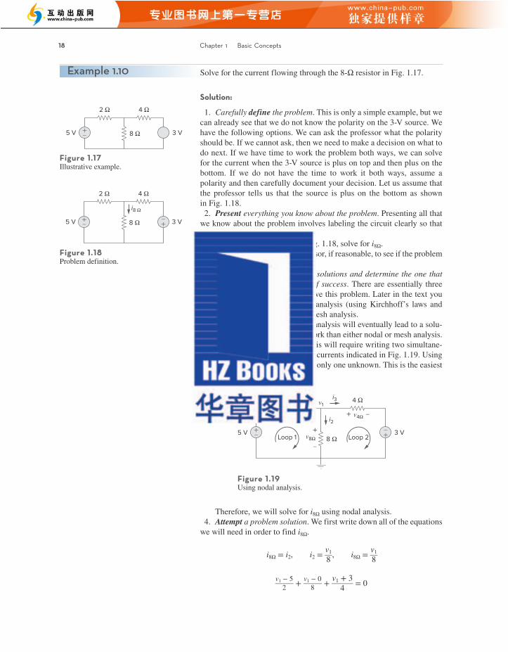
Solve for the current flowing through the 8-Ω resistor in Fig. 1.17.
Solution:
1. Carefully define the problem. This is only a simple example, but we can already see that we do not know the polarity on the 3-V source. We have the following options. We can ask the professor what the polarity should be. If we cannot ask, then we need to make a decision on what to do next. If we have time to work the problem both ways, we can solve for the current when the 3-V source is plus on top and then plus on the bottom. If we do not have the time to work it both ways, assume a polarity and then carefully document your decision. Let us assume that the professor tells us that the source is plus on the bottom as shown in Fig. 1.18.2. Present everything you know about the problem. Presenting all that
we know about the problem involves labeling the circuit clearly so that we define what we seek.
Given the circuit shown in Fig. 1.18, solve for i8Ω.We now check with the professor, if reasonable, to see if the problem
is properly defined.3. Establish a set of alternative solutions and determine the one that
promises the greatest likelihood of success. There are essentially three techniques that can be used to solve this problem. Later in the text you will see that you can use circuit analysis (using Kirchhoff’s laws and Ohm’s law), nodal analysis, and mesh analysis.
To solve for i8Ω using circuit analysis will eventually lead to a solu-tion, but it will likely take more work than either nodal or mesh analysis. To solve for i8Ω using mesh analysis will require writing two simultane-ous equations to find the two loop currents indicated in Fig. 1.19. Using nodal analysis requires solving for only one unknown. This is the easiest approach.
2 Ω 4 Ω
8 Ω5 V 3 V+– +
–i2
i1 i3
+ – + –
+
–v8Ω
v4Ωv2Ω
Loop 1 Loop 2
v1
Figure 1.19Using nodal analysis.
Therefore, we will solve for i8Ω using nodal analysis.4. Attempt a problem solution. We first write down all of the equations
we will need in order to find i8Ω.
i 8Ω = i 2 , i 2 = v1 __ 8 , i 8Ω = v 1 __ 8
v1 − 5 _____ 2 + v1 − 0
_____ 8 + v 1 + 3 ______ 4 = 0
aLe26409_ch01_002-028.indd 21 9/27/19 1:21 PM
18 Chapter 1 Basic Concepts
Figure 1.18Problem definition.
2 Ω 4 Ω
8 Ω5 V 3 V+– +–
i8 Ω
Figure 1.17Illustrative example.
2 Ω 4 Ω
8 Ω5 V 3 V+–
Example 1.10
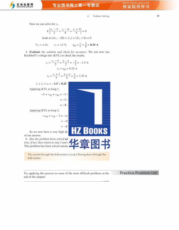
Now we can solve for v1.
8 [ v1 − 5 ______ 2 + v1 − 0 ______ 8 + v1 + 3 ______ 4 ] = 0
leads to (4 v 1 − 20) + ( v 1 ) + (2 v 1 + 6) = 0
7v1 = +14, v 1 = +2 V, i 8Ω = v1 __ 8 = 2 __ 8 = 0.25 A
5. Evaluate the solution and check for accuracy. We can now use Kirchhoff’s voltage law (KVL) to check the results.
i 1 = v1 − 5 _____ 2 = 2 − 5 ___ 2 = − 3 __ 2 = −1.5 A
i2 = i8Ω = 0.25 A
i 3 = v1 + 3 ______ 4 = 2 + 3 ___ 4 = 5 __ 4 = 1.25 A
i1 + i2 + i3 = −1.5 + 0.25 + 1.25 = 0 (Checks.)
Applying KVL to loop 1,
−5 + v 2Ω + v 8Ω = −5 + (− i 1 × 2) + ( i 2 × 8) = −5 + [− (−1.5) 2] + (0.25 × 8)
= −5 + 3 + 2 = 0 (Checks.)
Applying KVL to loop 2,
− v 8Ω + v 4Ω − 3 = − ( i 2 × 8) + ( i 3 × 4) − 3
= − (0.25 × 8) + (1.25 × 4) − 3
= −2 + 5 − 3 = 0 (Checks.)
So we now have a very high degree of confidence in the accuracy of our answer.6. Has the problem been solved satisfactorily? If so, present the solu-
tion; if not, then return to step 3 and continue through the process again. This problem has been solved satisfactorily.
The current through the 8-Ω resistor is 0.25 A flowing down through the 8-Ω resistor.
Try applying this process to some of the more difficult problems at the end of the chapter.
aLe26409_ch01_002-028.indd 22 9/27/19 1:21 PM
1.7 Problem Solving 19
Practice Problem 1.10
Solve for the current flowing through the 8-Ω resistor in Fig. 1.17.
Solution:
1. Carefully define the problem. This is only a simple example, but we can already see that we do not know the polarity on the 3-V source. We have the following options. We can ask the professor what the polarity should be. If we cannot ask, then we need to make a decision on what to do next. If we have time to work the problem both ways, we can solve for the current when the 3-V source is plus on top and then plus on the bottom. If we do not have the time to work it both ways, assume a polarity and then carefully document your decision. Let us assume that the professor tells us that the source is plus on the bottom as shown in Fig. 1.18.2. Present everything you know about the problem. Presenting all that
we know about the problem involves labeling the circuit clearly so that we define what we seek.
Given the circuit shown in Fig. 1.18, solve for i8Ω.We now check with the professor, if reasonable, to see if the problem
is properly defined.3. Establish a set of alternative solutions and determine the one that
promises the greatest likelihood of success. There are essentially three techniques that can be used to solve this problem. Later in the text you will see that you can use circuit analysis (using Kirchhoff’s laws and Ohm’s law), nodal analysis, and mesh analysis.
To solve for i8Ω using circuit analysis will eventually lead to a solu-tion, but it will likely take more work than either nodal or mesh analysis. To solve for i8Ω using mesh analysis will require writing two simultane-ous equations to find the two loop currents indicated in Fig. 1.19. Using nodal analysis requires solving for only one unknown. This is the easiest approach.
2 Ω 4 Ω
8 Ω5 V 3 V+– +
–i2
i1 i3
+ – + –
+
–v8Ω
v4Ωv2Ω
Loop 1 Loop 2
v1
Figure 1.19Using nodal analysis.
Therefore, we will solve for i8Ω using nodal analysis.4. Attempt a problem solution. We first write down all of the equations
we will need in order to find i8Ω.
i 8Ω = i 2 , i 2 = v1 __ 8 , i 8Ω = v 1 __ 8
v1 − 5 _____ 2 + v1 − 0
_____ 8 + v 1 + 3 ______ 4 = 0
aLe26409_ch01_002-028.indd 21 9/27/19 1:21 PM
18 Chapter 1 Basic Concepts
Figure 1.18Problem definition.
2 Ω 4 Ω
8 Ω5 V 3 V+– +–
i8 Ω
Figure 1.17Illustrative example.
2 Ω 4 Ω
8 Ω5 V 3 V+–
Example 1.10
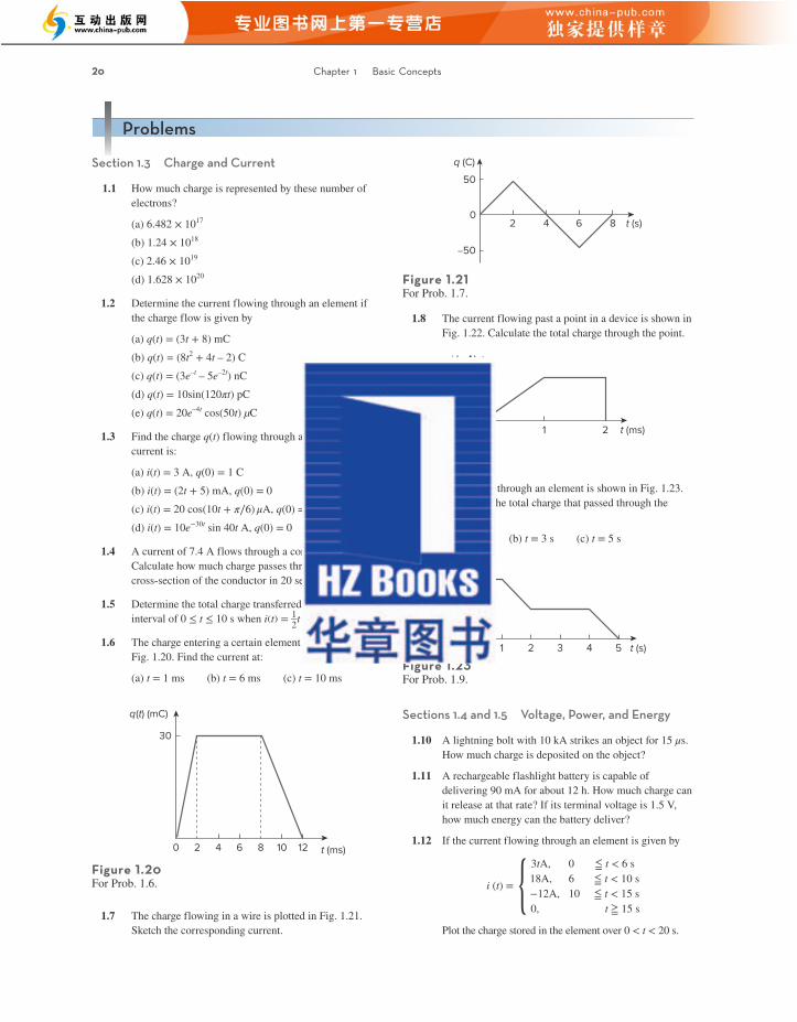
1.13 The charge entering the positive terminal of an element is
q = 5 sin 4 π t mC
while the voltage across the element (plus to minus) is
v = 3 cos 4 π t V
(a) Find the power delivered to the element at t = 0.3 s.
(b) Calculate the energy delivered to the element between 0 and 0.6 s.
1.14 The voltage v(t) across a device and the current i(t) through it are
v(t) = 10cos(2t) V, i(t) = 20(1 − e−0.5t) mA
Calculate:
(a) the total charge in the device at t = 1 s, q(0) = 0.(b) the power consumed by the device at t = 1 s.
1.15 The current entering the positive terminal of a device is i(t) = 6e−2t mA and the voltage across the device is v(t) = 10di∕dtV.
(a) Find the charge delivered to the device between t = 0 and t = 2 s.
(b) Calculate the power absorbed.(c) Determine the energy absorbed between t = 0
and t = 3 s.
Section 1.6 Circuit Elements
1.16 Figure 1.24 shows the current through and the voltage across an element.
(a) Sketch the power delivered to the element for t > 0.
(b) Find the total energy absorbed by the element for the period of 0 < t < 4s.
Figure 1.24For Prob. 1.16.
v (V)
t (s)
5
–5
020 4
i (mA)
t (s)
60
0 2 4
Problems 21
1.17 Figure 1.25 shows a circuit with five elements. If p1 = –205 W, p2 = 60 W, p4 = 45 W, and p5 = 30 W, calculate the power p3 absorbed by element 3.
Figure 1.28For Prob. 1.20.
6 A
6 A
1 A
3 A
3 A
Vo 5Io
Io = 2 A
28 V
12 V
+
–
+ –
28 V+ –
+ –
30 V –+
+–
Figure 1.27For Prob. 1.19.
8 A 9 V 9 V
6 V
2 A
+
– –
+ 3 V
i
–
+
+–
Figure 1.26For Prob. 1.18.
14 A
4 AI = 10 A
p1 p3
p4p2
p50.4I 20 V30 V +–
+
–12 V
+
–
10 V+ –
8 V+ –
Figure 1.25For Prob. 1.17.
42
31 5
1.18 Find the power absorbed by each of the elements in Fig. 1.26.
1.19 Find i and the power absorbed by each element in the network of Fig. 1.27.
1.20 Find Vo and the power absorbed by each element in the circuit of Fig. 1.28.
aLe26409_ch01_002-028.indd 25 9/27/19 1:21 PM
20 Chapter 1 Basic Concepts
Problems
Section 1.3 Charge and Current
1.1 How much charge is represented by these number of electrons?
(a) 6.482 × 10¹⁷
(b) 1.24 × 10¹⁸
(c) 2.46 × 10¹⁹
(d) 1.628 × 10²⁰
1.2 Determine the current flowing through an element if the charge flow is given by
(a) q(t) = (3t + 8) mC(b) q(t) = (8t2 + 4t – 2) C(c) q(t) = (3e–t – 5e–2t) nC(d) q(t) = 10sin(120πt) pC(e) q(t) = 20e–4t cos(50t) µC
1.3 Find the charge q(t) flowing through a device if the current is:
(a) i(t) = 3 A, q(0) = 1 C(b) i (t) = (2t + 5) mA, q (0) = 0(c) i (t) = 20 cos (10t + π∕6) μA, q (0) = 2 μC(d) i (t) = 10 e −30t sin 40t A, q (0) = 0
1.4 A current of 7.4 A flows through a conductor. Calculate how much charge passes through any cross-section of the conductor in 20 seconds.
1.5 Determine the total charge transferred over the time interval of 0 ≤ t ≤ 10 s when i (t) = 1 __ 2 t A.
1.6 The charge entering a certain element is shown in Fig. 1.20. Find the current at:
(a) t = 1 ms (b) t = 6 ms (c) t = 10 ms
Figure 1.20For Prob. 1.6.
q(t) (mC)
t (ms)0 2 4 6 8 10 12
30
1.7 The charge flowing in a wire is plotted in Fig. 1.21. Sketch the corresponding current.
Figure 1.21For Prob. 1.7.
t (s)2 4 6 8
q (C)
50
–50
0
1.8 The current flowing past a point in a device is shown in Fig. 1.22. Calculate the total charge through the point.
Figure 1.22For Prob. 1.8.
i (mA)
t (ms)0 1 2
10
1.9 The current through an element is shown in Fig. 1.23. Determine the total charge that passed through the element at:
(a) t = 1 s (b) t = 3 s (c) t = 5 s
Figure 1.23For Prob. 1.9.
0 1 2 3 4 5
5
10i (A)
t (s)
Sections 1.4 and 1.5 Voltage, Power, and Energy
1.10 A lightning bolt with 10 kA strikes an object for 15 μs. How much charge is deposited on the object?
1.11 A rechargeable flashlight battery is capable of delivering 90 mA for about 12 h. How much charge can it release at that rate? If its terminal voltage is 1.5 V, how much energy can the battery deliver?
1.12 If the current flowing through an element is given by
i (t) = 3tA, 0 ≦ t < 6 s18A, 6 ≦ t < 10 s−12A, 10 ≦ t < 15 s0, t ≧ 15 s
Plot the charge stored in the element over 0 < t < 20 s.
aLe26409_ch01_002-028.indd 24 9/27/19 1:21 PM

23
Enhancing Your Skills and Your Career
ABET EC 2000 criteria (3.b), “an ability to design and conduct experiments, as well as to analyze and interpret data.”Engineers must be able to design and conduct experiments, as well as analyze and interpret data. Most students have spent many hours per-forming experiments in high school and in college. During this time, you have been asked to analyze the data and to interpret the data. Therefore, you should already be skilled in these two activities. My recommenda-tion is that, in the process of performing experiments in the future, you spend more time in analyzing and interpreting the data in the context of the experiment. What does this mean?
If you are looking at a plot of voltage versus resistance or current versus resistance or power versus resistance, what do you actually see? Does the curve make sense? Does it agree with what the theory tells you? Does it differ from expectation, and, if so, why? Clearly, practice with analyzing and interpreting data will enhance this skill.
Since most, if not all, the experiments you are required to do as a student involve little or no practice in designing the experiment, how can you develop and enhance this skill?
Actually, developing this skill under this constraint is not as difficult as it seems. What you need to do is to take the experiment and analyze it. Just break it down into its simplest parts, reconstruct it trying to under-stand why each element is there, and finally, determine what the author of the experiment is trying to teach you. Even though it may not always seem so, every experiment you do was designed by someone who was sincerely motivated to teach you something.
c h a p t e r
2Basic LawsThere are too many people praying for mountains of difficulty to be removed, when what they really need is the courage to climb them!
—Unknown
aLe26409_ch02_029-078.indd 29 9/27/19 2:29 PM
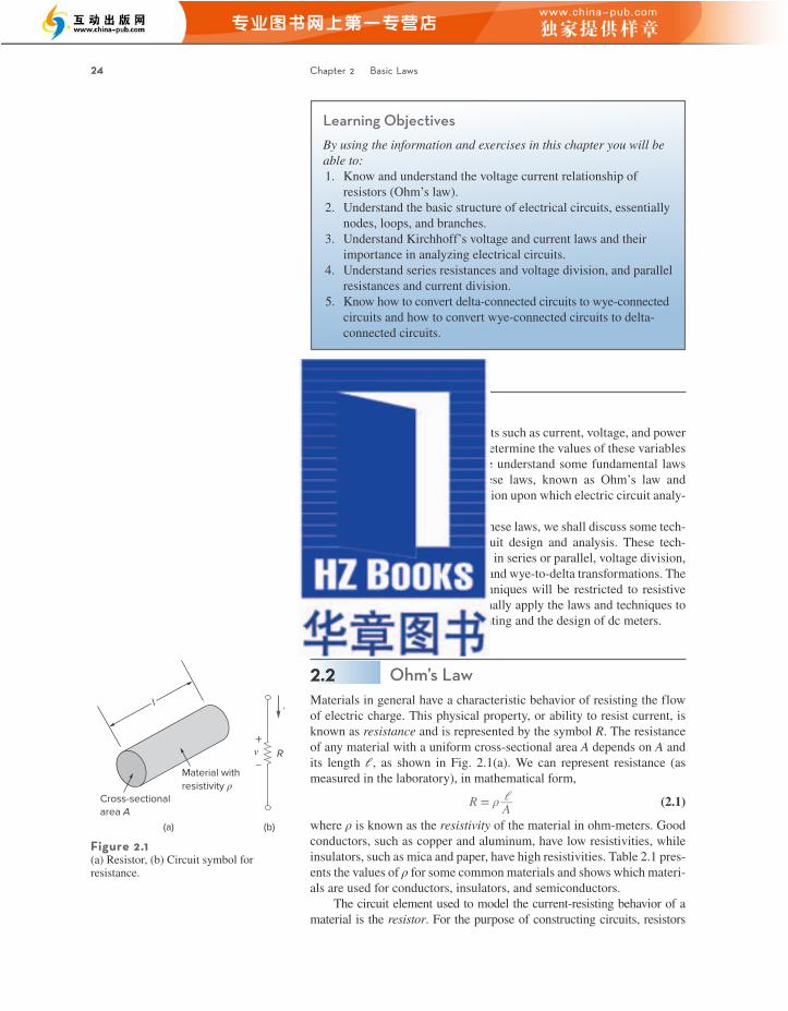
2.2 Ohm’s Law 25
are usually made from metallic alloys and carbon compounds. The circuit symbol for the resistor is shown in Fig. 2.1(b), where R stands for the resis-tance of the resistor. The resistor is the simplest passive element.
Georg Simon Ohm (1787–1854), a German physicist, is credited with finding the relationship between current and voltage for a resistor. This relationship is known as Ohm’s law.
Ohm’s law states that the voltage v across a resistor is directly propor-tional to the current i flowing through the resistor.
That is,
v ∝ i (2.2)
Ohm defined the constant of proportionality for a resistor to be the resis-tance, R. (The resistance is a material property which can change if the internal or external conditions of the element are altered, e.g., if there are changes in the temperature.) Thus, Eq. (2.2) becomes
v = iR (2.3)
TABLE 2.1
Resistivities of common materials.
Material Resistivity (Ω∙m) UsageSilver 1.64 × 10⁻⁸ ConductorCopper 1.72 × 10⁻⁸ ConductorAluminum 2.8 × 10⁻⁸ ConductorGold 2.45 × 10⁻⁸ ConductorCarbon 4 × 10⁻⁵ SemiconductorGermanium 47 × 10−2 SemiconductorSilicon 6.4 × 10² SemiconductorPaper 1010 InsulatorMica 5 × 10¹¹ InsulatorGlass 1012 InsulatorTeflon 3 × 10¹² Insulator
Georg Simon Ohm (1787–1854), a German physicist, in 1826 experimentally determined the most basic law relating voltage and cur-rent for a resistor. Ohm’s work was initially denied by critics.
Born of humble beginnings in Erlangen, Bavaria, Ohm threw him-self into electrical research. His efforts resulted in his famous law. He was awarded the Copley Medal in 1841 by the Royal Society of London. In 1849, he was given the Professor of Physics chair by the University of Munich. To honor him, the unit of resistance was named the ohm.
Historical
SSPL
via
Get
ty Im
ages
aLe26409_ch02_029-078.indd 31 9/27/19 2:29 PM
24 Chapter 2 Basic Laws
2.1 IntroductionChapter 1 introduced basic concepts such as current, voltage, and power in an electric circuit. To actually determine the values of these variables in a given circuit requires that we understand some fundamental laws that govern electric circuits. These laws, known as Ohm’s law and Kirchhoff’s laws, form the foundation upon which electric circuit analy-sis is built.
In this chapter, in addition to these laws, we shall discuss some tech-niques commonly applied in circuit design and analysis. These tech-niques include combining resistors in series or parallel, voltage division, current division, and delta-to-wye and wye-to-delta transformations. The application of these laws and techniques will be restricted to resistive circuits in this chapter. We will finally apply the laws and techniques to real-life problems of electrical lighting and the design of dc meters.
2.2 Ohm’s LawMaterials in general have a characteristic behavior of resisting the flow of electric charge. This physical property, or ability to resist current, is known as resistance and is represented by the symbol R. The resistance of any material with a uniform cross-sectional area A depends on A and its length ℓ, as shown in Fig. 2.1(a). We can represent resistance (as measured in the laboratory), in mathematical form,
R = ρ 𝓁𝓁 __ A
(2.1)
where ρ is known as the resistivity of the material in ohm-meters. Good conductors, such as copper and aluminum, have low resistivities, while insulators, such as mica and paper, have high resistivities. Table 2.1 pres-ents the values of ρ for some common materials and shows which materi-als are used for conductors, insulators, and semiconductors.
The circuit element used to model the current-resisting behavior of a material is the resistor. For the purpose of constructing circuits, resistors
Learning ObjectivesBy using the information and exercises in this chapter you will be able to:1. Know and understand the voltage current relationship of
resistors (Ohm’s law).2. Understand the basic structure of electrical circuits, essentially
nodes, loops, and branches.3. Understand Kirchhoff’s voltage and current laws and their
importance in analyzing electrical circuits.4. Understand series resistances and voltage division, and parallel
resistances and current division.5. Know how to convert delta-connected circuits to wye-connected
circuits and how to convert wye-connected circuits to delta-connected circuits.
l
Cross-sectionalarea A
(a)
Material withresistivity ρ
v R
i
+
–
(b)
Figure 2.1(a) Resistor, (b) Circuit symbol for resistance.
aLe26409_ch02_029-078.indd 30 9/27/19 2:29 PM
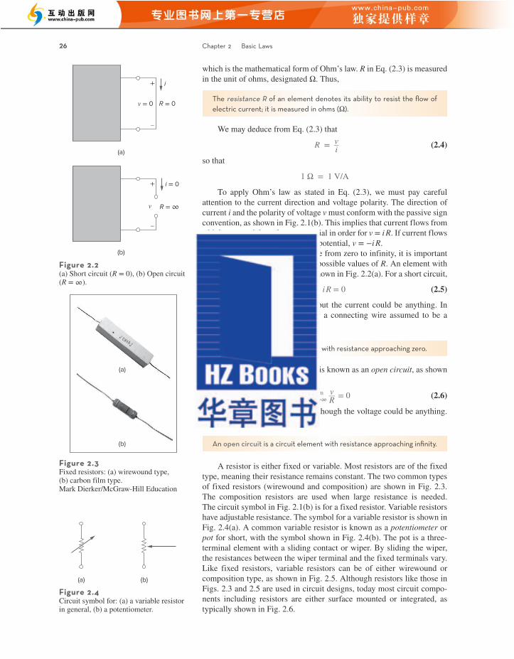
2.2 Ohm’s Law 27
It should be pointed out that not all resistors obey Ohm’s law. A re-sistor that obeys Ohm’s law is known as a linear resistor. It has a constant resistance and thus its current-voltage characteristic is as illustrated in Fig. 2.7(a): Its i-v graph is a straight line passing through the origin. A nonlinear resistor does not obey Ohm’s law. Its resistance varies with current and its i-v characteristic is typically shown in Fig. 2.7(b). Examples of devices with nonlinear resistance are the light bulb and the diode. Although all practical resistors may exhibit nonlinear behavior under certain conditions, we will assume in this book that all elements actually designated as resistors are linear.
A useful quantity in circuit analysis is the reciprocal of resistance R, known as conductance and denoted by G:
G = 1 __ R
= i __ v (2.7)
The conductance is a measure of how well an element will conduct electric current. The unit of conductance is the mho (ohm spelled back-ward) or reciprocal ohm, with symbol , the inverted omega. Although engineers often use the mho, in this book we prefer to use the siemens (S), the SI unit of conductance:
1 S = 1 = 1 A / V (2.8)Thus,
Conductance is the ability of an element to conduct electric current; it is measured in mhos () or siemens (S).
The same resistance can be expressed in ohms or siemens. For example, 10 Ω is the same as 0.1 S. From Eq. (2.7), we may write
i = Gv (2.9)
The power dissipated by a resistor can be expressed in terms of R. Using Eqs. (1.7) and (2.3),
p = vi = i 2 R = v 2 __ R
(2.10)
(a) (b)
Figure 2.5Variable resistors: (a) composition type, (b) slider pot. Mark Dierker/McGraw-Hill Education
Figure 2.6Resistors in an integrated circuit board.
Eric
Tor
mey
/Ala
my
Slope = R
(a)
v
i
Slope = R
(b)
v
i
Figure 2.7The i-v characteristic of: (a) a linear resistor, (b) a nonlinear resistor.
aLe26409_ch02_029-078.indd 33 9/27/19 2:30 PM
26 Chapter 2 Basic Laws
which is the mathematical form of Ohm’s law. R in Eq. (2.3) is mea sured in the unit of ohms, designated Ω. Thus,
The resistance R of an element denotes its ability to resist the flow of electric current; it is measured in ohms (Ω).
We may deduce from Eq. (2.3) that
R = v __ i (2.4)
so that
1 Ω = 1 V/A
To apply Ohm’s law as stated in Eq. (2.3), we must pay careful attention to the current direction and voltage polarity. The direction of current i and the polarity of voltage v must conform with the passive sign convention, as shown in Fig. 2.1(b). This implies that current flows from a higher potential to a lower potential in order for v = i R. If current flows from a lower potential to a higher potential, v = −i R.
Since the value of R can range from zero to infinity, it is important that we consider the two extreme possible values of R. An element with R = 0 is called a short circuit, as shown in Fig. 2.2(a). For a short circuit,
v = i R = 0 (2.5)
showing that the voltage is zero but the current could be anything. In practice, a short circuit is usually a connecting wire assumed to be a perfect conductor. Thus,
A short circuit is a circuit element with resistance approaching zero.
Similarly, an element with R = ∞ is known as an open circuit, as shown in Fig. 2.2(b). For an open circuit,
i = lim R→∞ v __ R
= 0 (2.6)
indicating that the current is zero though the voltage could be anything. Thus,
An open circuit is a circuit element with resistance approaching infinity.
A resistor is either fixed or variable. Most resistors are of the fixed type, meaning their resistance remains constant. The two common types of fixed resistors (wirewound and composition) are shown in Fig. 2.3. The composition resistors are used when large resistance is needed. The circuit symbol in Fig. 2.1(b) is for a fixed resistor. Variable resistors have adjustable resistance. The symbol for a variable resistor is shown in Fig. 2.4(a). A common variable resistor is known as a potentiometer or pot for short, with the symbol shown in Fig. 2.4(b). The pot is a three-terminal element with a sliding contact or wiper. By sliding the wiper, the resistances between the wiper terminal and the fixed terminals vary. Like fixed resistors, variable resistors can be of either wirewound or composition type, as shown in Fig. 2.5. Although resistors like those in Figs. 2.3 and 2.5 are used in circuit designs, today most circuit compo-nents including resistors are either surface mounted or integrated, as typically shown in Fig. 2.6.
(a)
(b)
R = 0
i
R = ∞
i = 0
v = 0
+
–
v
+
–
Figure 2.2(a) Short circuit (R = 0), (b) Open circuit (R = ∞).
(a)
(b)
Figure 2.3Fixed resistors: (a) wirewound type, (b) carbon film type.Mark Dierker/McGraw-Hill Education
(a) (b)
Figure 2.4Circuit symbol for: (a) a variable resistor in general, (b) a potentiometer.
aLe26409_ch02_029-078.indd 32 9/27/19 2:30 PM
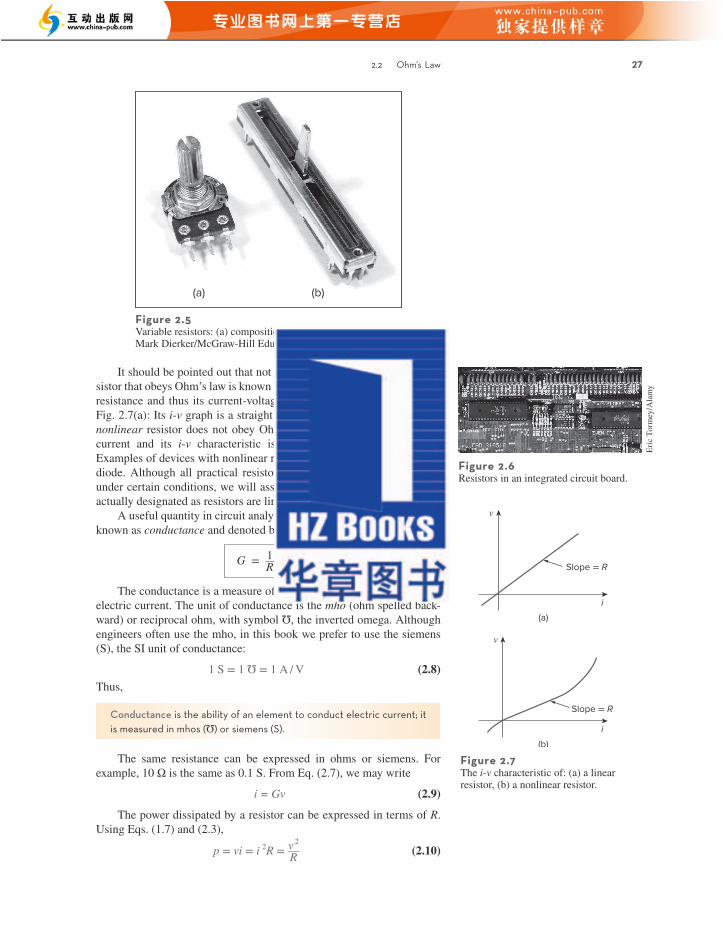
2.3 Nodes, Branches, and Loops 29
Figure 2.9For Practice Prob. 2.2
3 mA
i
10 kΩ v+
–
Example 2.3A voltage source of 20 sin πt V is connected across a 5-kΩ resistor. Find the current through the resistor and the power dissipated.
Solution:
i = v __ R
= 20 sinπt _______ 5 × 10 3
= 4 sinπt mA
Hence, p = vi = 80 sin 2 π t mW
Practice Problem 2.3A resistor absorbs an instantaneous power of 30 cos2 t mW when con-nected to a voltage source v = 15 cos t V. Find i and R.
Answer: 2 cos t mA, 7.5 kΩ.
For the circuit shown in Fig. 2.9, calculate the voltage v, the conductance G, and the power p.
Answer: 30 V, 100 µS, 90 mW.
Practice Problem 2.2
2.3 Nodes, Branches, and LoopsSince the elements of an electric circuit can be interconnected in several ways, we need to understand some basic concepts of network topology. To differentiate between a circuit and a network, we may regard a network as an interconnection of elements or devices, whereas a circuit is a network providing one or more closed paths. The convention, when addressing network topology, is to use the word network rather than circuit. We do this even though the word network and circuit mean the same thing when used in this context. In network topology, we study the properties relating to the placement of elements in the network and the geometric configura-tion of the network. Such elements include branches, nodes, and loops.
A branch represents a single element such as a voltage source or a resistor.
In other words, a branch represents any two-terminal element. The cir-cuit in Fig. 2.10 has five branches, namely, the 10-V voltage source, the 2-A current source, and the three resistors.
A node is the point of connection between two or more branches.
A node is usually indicated by a dot in a circuit. If a short circuit (a connecting wire) connects two nodes, the two nodes constitute a single node. The circuit in Fig. 2.10 has three nodes a, b, and c. Notice that the
10 V 2 A
a b
c
5 Ω
+– 2 Ω 3 Ω
Figure 2.10Nodes, branches, and loops.
aLe26409_ch02_029-078.indd 35 9/27/19 2:30 PM
28 Chapter 2 Basic Laws
The power dissipated by a resistor may also be expressed in terms of G as
p = vi = v2G = i2 __
G (2.11)
We should note two things from Eqs. (2.10) and (2.11):
1. The power dissipated in a resistor is a nonlinear function of either current or voltage.
2. Since R and G are positive quantities, the power dissipated in a resis-tor is always positive. Thus, a resistor always absorbs power from the circuit. This confirms the idea that a resistor is a passive ele-ment, incapable of generating energy.
An electric iron draws 2 A at 120 V. Find its resistance.
Solution:From Ohm’s law,
R = v _ i = 120 ___ 2 = 60 Ω
Example 2.1
The essential component of a toaster is an electrical element (a resistor) that converts electrical energy to heat energy. How much current is drawn by a toaster with resistance 15 Ω at 110 V?
Answer: 7.333 A.
Practice Problem 2.1
In the circuit shown in Fig. 2.8, calculate the current i, the conductance G, and the power p.
Solution:The voltage across the resistor is the same as the source voltage (30 V) because the resistor and the voltage source are connected to the same pair of terminals. Hence, the current is
i = v __ R
= 30 _____ 5 × 10 3
= 6 mA
The conductance is
G = 1 __ R
= 1 _____ 5 × 10 3
= 0.2 mS
We can calculate the power in various ways using either Eqs. (1.7), (2.10), or (2.11).
p = vi = 30 (6 × 10 −3 ) = 180 mW or
p = i 2 R = (6 × 10 −3 ) 2 5 × 10 3 = 180 mW or
p = v 2 G = (30) 2 0.2 × 10 −3 = 180 mW
Example 2.2
30 V
i
+– 5 kΩ v
+
–
Figure 2.8For Example 2.2.
aLe26409_ch02_029-078.indd 34 9/27/19 2:30 PM
2.4 Kirchhoff’s Laws 31
2.4 Kirchhoff’s LawsOhm’s law by itself is not sufficient to analyze circuits. However, when it is coupled with Kirchhoff’s two laws, we have a sufficient, powerful set of tools for analyzing a large variety of electric circuits. Kirchhoff’s laws were first introduced in 1847 by the German physicist Gustav Robert Kirchhoff (1824–1887). These laws are formally known as Kirchhoff’s current law (KCL) and Kirchhoff’s voltage law (KVL).
Kirchhoff’s first law is based on the law of conservation of charge, which requires that the algebraic sum of charges within a system cannot change.
Kirchhoff’s current law (KCL) states that the algebraic sum of currents entering a node (or a closed boundary) is zero.
Mathematically, KCL implies that
∑ n=1
N i n = 0 (2.13)
where N is the number of branches connected to the node and in is the nth current entering (or leaving) the node. By this law, currents entering a node may be regarded as positive, while currents leaving the node may be taken as negative or vice versa.
5 Ω
6 Ω 2 A10 V +–
Figure 2.12For Example 2.4.
1 25 Ω
6 Ω 2 A10 V +–
3
Figure 2.13The three nodes in the circuit of Fig. 2.12.
Practice Problem 2.4How many branches and nodes does the circuit in Fig. 2.14 have? Identify the elements that are in series and in parallel.
Answer: Five branches and three nodes are identified in Fig. 2.15. The 1-Ω and 2-Ω resistors are in parallel. The 4-Ω resistor and 10-V source are also in parallel.
5 Ω
1 Ω 2 Ω 4 Ω10 V+–
Figure 2.14For Practice Prob. 2.4.
5 Ω
3
1 Ω 2 Ω 4 Ω10 V+–
1 2
Figure 2.15Answer for Practice Prob. 2.4.
aLe26409_ch02_029-078.indd 37 9/27/19 2:30 PM
30 Chapter 2 Basic Laws
three points that form node b are connected by perfectly conducting wires and therefore constitute a single point. The same is true of the four points forming node c. We demonstrate that the circuit in Fig. 2.10 has only three nodes by redrawing the circuit in Fig. 2.11. The two circuits in Figs. 2.10 and 2.11 are identical. However, for the sake of clarity, nodes b and c are spread out with perfect conductors as in Fig. 2.10.
A loop is any closed path in a circuit.
A loop is a closed path formed by starting at a node, passing through a set of nodes, and returning to the starting node without passing through any node more than once. A loop is said to be independent if it contains at least one branch which is not a part of any other independent loop. Independent loops or paths result in independent sets of equations.
It is possible to form an independent set of loops where one of the loops does not contain such a branch. In Fig. 2.11, abca with the 2Ω resis-tor is independent. A second loop with the 3Ω resistor and the current source is independent. The third loop could be the one with the 2Ω resistor in parallel with the 3Ω resistor. This does form an independent set of loops.
A network with b branches, n nodes, and l independent loops will satisfy the fundamental theorem of network topology:
b = l + n − 1 (2.12)
As the next two definitions show, circuit topology is of great value to the study of voltages and currents in an electric circuit.
Two or more elements are in series if they exclusively share a single node and consequently carry the same current.Two or more elements are in parallel if they are connected to the same two nodes and consequently have the same voltage across them.
Elements are in series when they are chain-connected or connected se-quentially, end to end. For example, two elements are in series if they share one common node and no other element is connected to that common node. Elements in parallel are connected to the same pair of terminals. Elements may be connected in a way that they are neither in series nor in parallel. In the circuit shown in Fig. 2.10, the voltage source and the 5-Ω resistor are in series because the same current will flow through them. The 2-Ω resistor, the 3-Ω resistor, and the current source are in parallel because they are connected to the same two nodes b and c and consequently have the same voltage across them. The 5-Ω and 2-Ω resistors are neither in series nor in parallel with each other.
b
c
a
10 V
5 Ω
2 Ω3 Ω 2 A
+–
Figure 2.11The three-node circuit of Fig. 2.10 is redrawn.
Determine the number of branches and nodes in the circuit shown in Fig. 2.12. Identify which elements are in series and which are in parallel.
Solution:Since there are four elements in the circuit, the circuit has four branches: 10 V, 5 Ω, 6 Ω, and 2 A. The circuit has three nodes as identified in Fig. 2.13. The 5-Ω resistor is in series with the 10-V voltage source because the same current would flow in both. The 6-Ω resistor is in parallel with the 2-A current source because both are connected to the same nodes 2 and 3.
Example 2.4
aLe26409_ch02_029-078.indd 36 9/27/19 2:30 PM
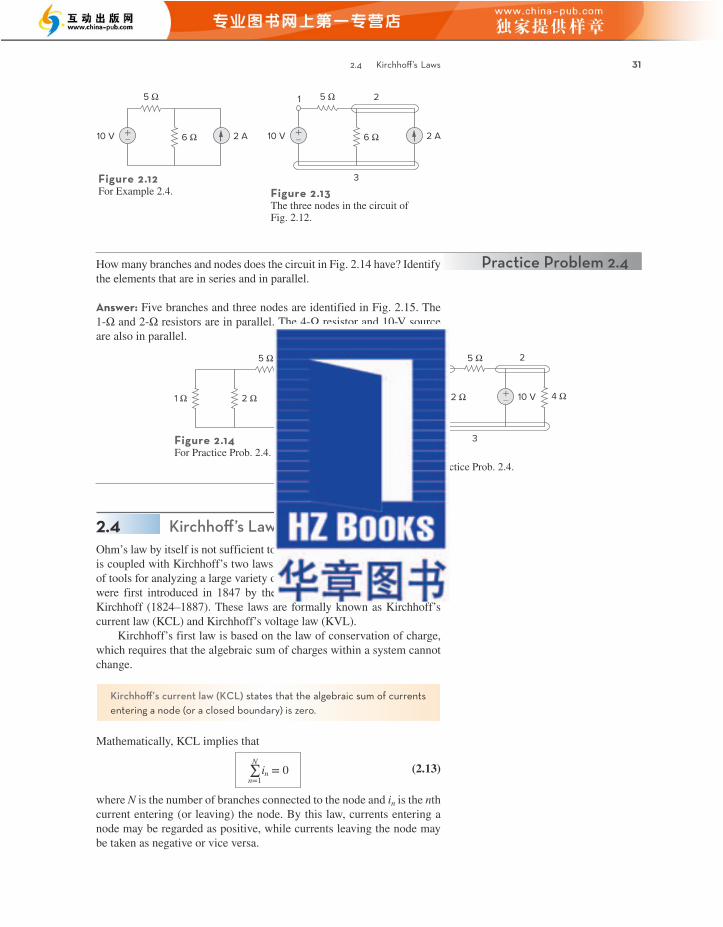
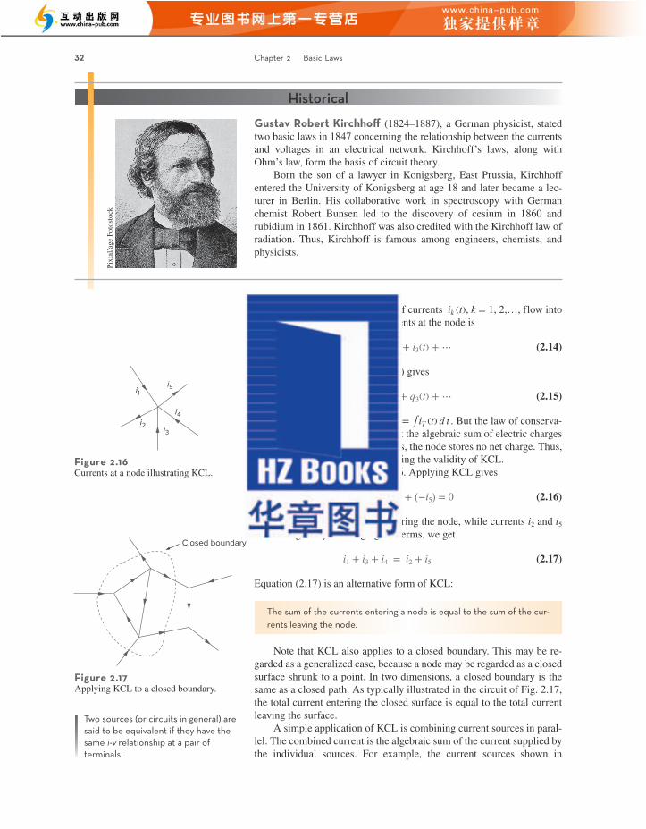
2.4 Kirchhoff’s Laws 33
Fig. 2.18(a) can be combined as in Fig. 2.18(b). The combined or equiv-alent current source can be found by applying KCL to node a.
IT + I2 = I1 + I3
or
I T = I 1 − I 2 + I 3 (2.18)
A circuit cannot contain two different currents, I1 and I2, in series, unless I1 = I2; otherwise KCL will be violated.
Kirchhoff’s second law is based on the principle of conservation of energy:
Kirchhoff’s voltage law (KVL) states that the algebraic sum of all volt-ages around a closed path (or loop) is zero.
Expressed mathematically, KVL states that
∑ m=1
M
v m = 0 (2.19)
where M is the number of voltages in the loop (or the number of branches in the loop) and vm is the mth voltage.
To illustrate KVL, consider the circuit in Fig. 2.19. The sign on each voltage is the polarity of the terminal encountered first as we travel around the loop. We can start with any branch and go around the loop either clockwise or counterclockwise. Suppose we start with the voltage source and go clockwise around the loop as shown; then voltages would be −v1, +v2, +v3, +v4, and −v5, in that order. For example, as we reach branch 3, the positive terminal is met first; hence, we have +v3. For branch 4, we reach the negative terminal first; hence, −v4. Thus, KVL yields
− v 1 + v 2 + v 3 − v 4 + v 5 = 0 (2.20)
Rearranging terms gives
v 2 + v 3 + v 5 = v 1 + v 4 (2.21)
which may be interpreted as
Sum of voltage drops = Sum of voltage rises (2.22)
This is an alternative form of KVL. Notice that if we had traveled coun-terclockwise, the result would have been +v1, −v5, +v4, −v3, and −v2, which is the same as before except that the signs are reversed. Hence, Eqs. (2.20) and (2.21) remain the same.
When voltage sources are connected in series, KVL can be applied to obtain the total voltage. The combined voltage is the algebraic sum of the voltages of the individual sources. For example, for the voltage sources shown in Fig. 2.20(a), the combined or equivalent voltage source in Fig. 2.20(b) is obtained by applying KVL.
− V ab + V 1 + V 2 − V 3 = 0
KVL can be applied in two ways: by taking either a clockwise or a counter-clockwise trip around the loop. Either way, the algebraic sum of voltages around the loop is zero.
a
(a)
(b)
I1 I2 I3
b
a
IT = I1 – I2 + I3
b
IT
IT
Figure 2.18Current sources in parallel: (a) original circuit, (b) equivalent circuit.
Figure 2.19A single-loop circuit illustrating KVL.
v4v1+– +
–
v3v2
v5
+ – + –
+–
aLe26409_ch02_029-078.indd 39 9/27/19 2:30 PM
32 Chapter 2 Basic Laws
To prove KCL, assume a set of currents i k (t) , k = 1, 2,…, flow into a node. The algebraic sum of currents at the node is
i T (t) = i 1 (t) + i 2 (t) + i 3 (t) + ⋯ (2.14)
Integrating both sides of Eq. (2.14) gives
q T (t) = q 1 (t) + q 2 (t) + q 3 (t) + ⋯ (2.15)
where q k (t) = ∫ i k (t) d t and q T (t) = ∫ i T (t) d t . But the law of conserva-tion of electric charge requires that the algebraic sum of electric charges at the node must not change; that is, the node stores no net charge. Thus, q T (t) = 0 → i T (t) = 0, confirming the validity of KCL.
Consider the node in Fig. 2.16. Applying KCL gives
i 1 + (− i 2 ) + i 3 + i 4 + (− i 5 ) = 0 (2.16)
since currents i1, i3, and i4 are entering the node, while currents i2 and i5 are leaving it. By rearranging the terms, we get
i 1 + i 3 + i 4 = i 2 + i 5 (2.17)
Equation (2.17) is an alternative form of KCL:
The sum of the currents entering a node is equal to the sum of the cur-rents leaving the node.
Note that KCL also applies to a closed boundary. This may be re-garded as a generalized case, because a node may be regarded as a closed surface shrunk to a point. In two dimensions, a closed boundary is the same as a closed path. As typically illustrated in the circuit of Fig. 2.17, the total current entering the closed surface is equal to the total current leaving the surface.
A simple application of KCL is combining current sources in paral-lel. The combined current is the algebraic sum of the current supplied by the individual sources. For example, the current sources shown in
Historical
Gustav Robert Kirchhoff (1824–1887), a German physicist, stated two basic laws in 1847 concerning the relationship between the currents and voltages in an electrical network. Kirchhoff’s laws, along with Ohm’s law, form the basis of circuit theory.
Born the son of a lawyer in Konigsberg, East Prussia, Kirchhoff entered the University of Konigsberg at age 18 and later became a lec-turer in Berlin. His collaborative work in spectroscopy with German chemist Robert Bunsen led to the discovery of cesium in 1860 and rubidium in 1861. Kirchhoff was also credited with the Kirchhoff law of radiation. Thus, Kirchhoff is famous among engineers, chemists, and physicists.
Pixt
al/a
ge F
otos
tock
i1i5
i4
i3i2
Figure 2.16Currents at a node illustrating KCL.
Closed boundary
Figure 2.17Applying KCL to a closed boundary.
Two sources (or circuits in general) are said to be equivalent if they have the same i-v relationship at a pair of terminals.
aLe26409_ch02_029-078.indd 38 9/27/19 2:30 PM
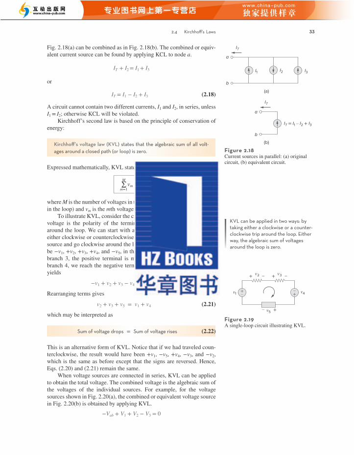
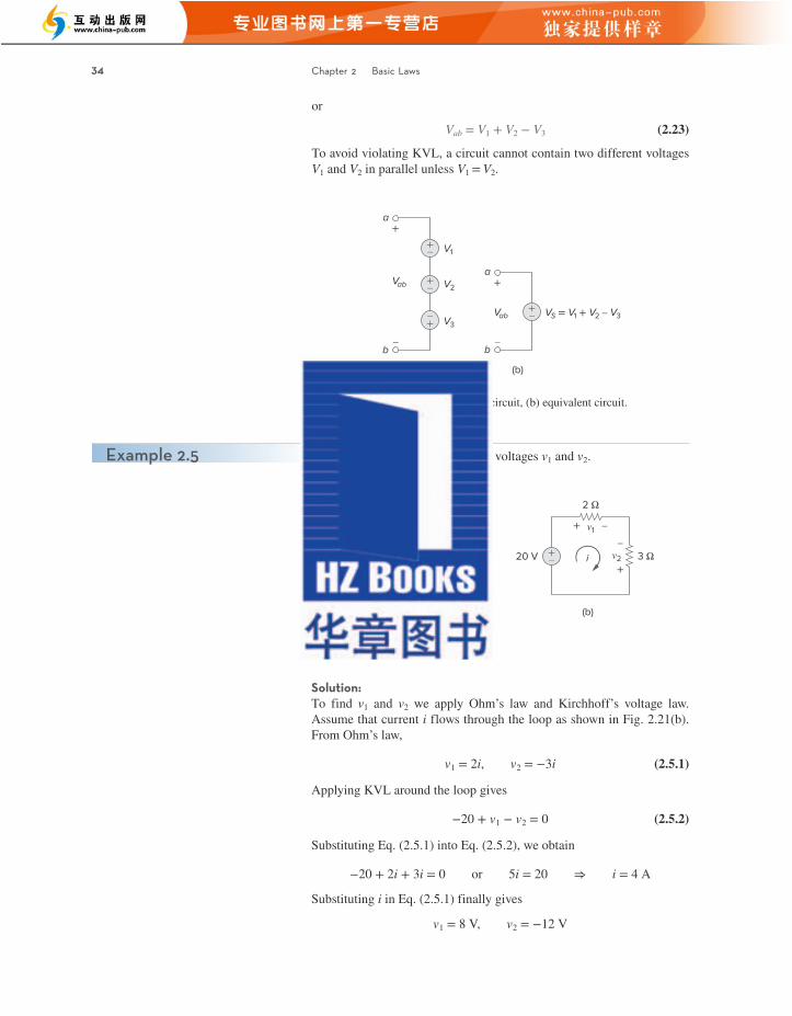
2.4 Kirchhoff’s Laws 35
Practice Problem 2.5Find v1 and v2 in the circuit of Fig. 2.22.
Answer: 16 V, −8 V.
Figure 2.22For Practice Prob. 2.5.
32 V +– –8 V+–
4 Ω
v1
2 Ω
v2
+ –
+ –
Example 2.6Determine vo and i in the circuit shown in Fig. 2.23(a).
Solution:We apply KVL around the loop as shown in Fig. 2.23(b). The result is
−12 + 4i + 2 v o − 4 + 6i = 0 (2.6.1)
Applying Ohm’s law to the 6-Ω resistor gives
v o = −6i (2.6.2)
Substituting Eq. (2.6.2) into Eq. (2.6.1) yields
−16 + 10i − 12i = 0 ⇒ i = −8 A
and vo = 48 V.
Figure 2.23For Example 2.6.
4 Ω
(a)
12 V
2vo
i4 V
i
+ –
+– +–
4 Ω
(b)
12 V
2vo
4 V
+ –
+– +–
6 Ω
vo
6 Ω
vo+ – + –
Practice Problem 2.6Find vx and vo in the circuit of Fig. 2.24.
Answer: 20 V, −10 V.
Figure 2.24For Practice Prob. 2.6.
70 V 2vx+–
+–
10 Ω
vx
5 Ω
vo+ –
+ –
aLe26409_ch02_029-078.indd 41 9/27/19 2:30 PM
34 Chapter 2 Basic Laws
or
V ab = V 1 + V 2 − V 3 (2.23)
To avoid violating KVL, a circuit cannot contain two different voltages V1 and V2 in parallel unless V1 = V2.
Figure 2.20Voltage sources in series: (a) original circuit, (b) equivalent circuit.
V1
V2
V3
a
b
(a)
VS = V1 + V2 – V3
a
b
(b)
+–
+–
+–Vab
+
–
Vab
+
–
+–
For the circuit in Fig. 2.21(a), find voltages v1 and v2.Example 2.5
Figure 2.21For Example 2.5.
(a)
20 V +– 3 Ωv2
2 Ω
v1+ –
+
–
(b)
20 V +– 3 Ωv2
2 Ω
v1+ –
+
–
i
Solution:To find v1 and v2 we apply Ohm’s law and Kirchhoff’s voltage law. Assume that current i flows through the loop as shown in Fig. 2.21(b). From Ohm’s law,
v 1 = 2i, v 2 = −3i (2.5.1)
Applying KVL around the loop gives
−20 + v 1 − v 2 = 0 (2.5.2)
Substituting Eq. (2.5.1) into Eq. (2.5.2), we obtain
−20 + 2i + 3i = 0 or 5i = 20 ⇒ i = 4 A
Substituting i in Eq. (2.5.1) finally gives
v 1 = 8 V, v 2 = −12 V
aLe26409_ch02_029-078.indd 40 9/27/19 2:30 PM
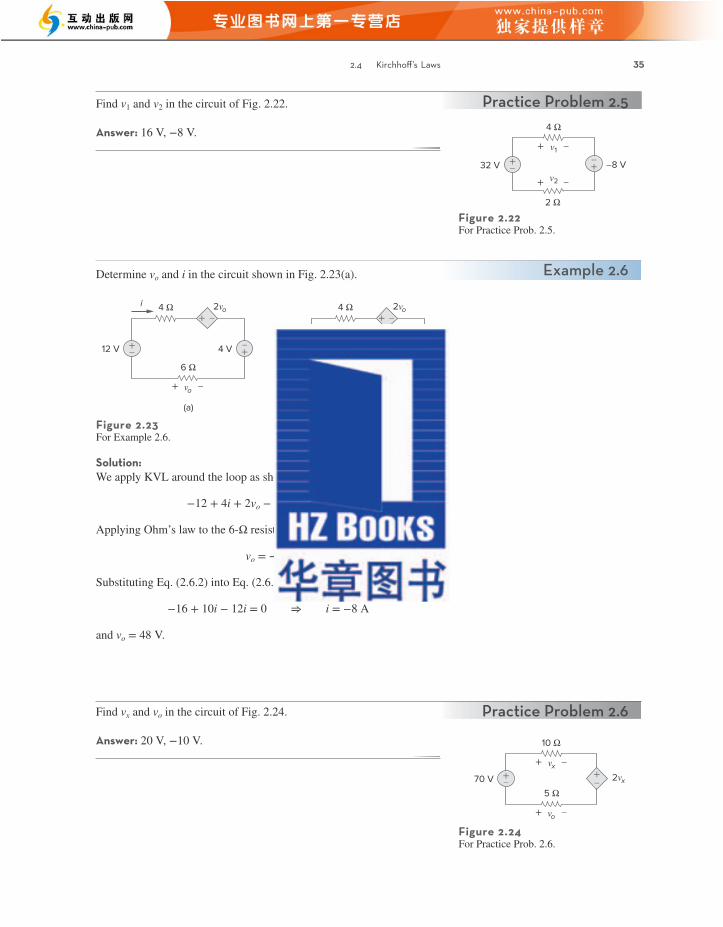
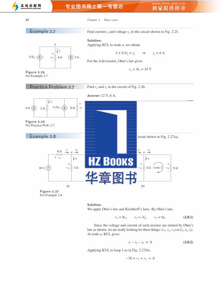
2.5 Series Resistors and Voltage Division 37
We express this in terms of i1 and i2 as in Eq. (2.8.1) to obtain
−30 + 8 i 1 + 3 i 2 = 0
or
i 1 = (30 − 3 i 2 ) ______ 8 (2.8.3)
Applying KVL to loop 2,
− v 2 + v 3 = 0 ⇒ v 3 = v 2 (2.8.4)
as expected since the two resistors are in parallel. We express v1 and v2 in terms of i1 and i2 as in Eq. (2.8.1). Equation (2.8.4) becomes
6 i 3 = 3 i 2 ⇒ i 3 = i 2 __ 2 (2.8.5)
Substituting Eqs. (2.8.3) and (2.8.5) into (2.8.2) gives
30 − 3 i 2 _____ 8 − i 2 − i 2 __ 2 = 0
or i2 = 2 A. From the value of i2, we now use Eqs. (2.8.1) to (2.8.5) to obtain
i 1 = 3 A, i 3 = 1 A, v 1 = 24 V, v 2 = 6 V, v 3 = 6 V
Practice Problem 2.8Find the currents and voltages in the circuit shown in Fig. 2.28.
Answer: v1 = 6 V, v2 = 4 V, v3 = 10 V, i1 = 3 A, i2 = 500 mA, i3 = 2.5 A.
Figure 2.28For Practice Prob. 2.8.
10 V 6 V+–
i2
i3i1
8 Ωv2
+
–
2 Ω
v1
4 Ω
v3
+–
+ – + –
2.5 Series Resistors and Voltage DivisionThe need to combine resistors in series or in parallel occurs so fre quently that it warrants special attention. The process of combining the resistors is facilitated by combining two of them at a time. With this in mind, consider the single-loop circuit of Fig. 2.29. The two resistors are in se-ries, since the same current i flows in both of them. Applying Ohm’s law to each of the resistors, we obtain
v 1 = i R 1 , v 2 = i R 2 (2.24)
If we apply KVL to the loop (moving in the clockwise direction), we have
−v + v 1 + v 2 = 0 (2.25)
Combining Eqs. (2.24) and (2.25), we get
v = v 1 + v 2 = i ( R 1 + R 2 ) (2.26)
or
i = v _____ R 1 + R 2 (2.27)
Figure 2.29A single-loop circuit with two resistors in series.
v +–
R1
v1
R2
v2
i
+ – + –
a
b
aLe26409_ch02_029-078.indd 43 9/27/19 2:30 PM
36 Chapter 2 Basic Laws
Find current io and voltage vo in the circuit shown in Fig. 2.25.
Solution:Applying KCL to node a, we obtain
3 + 0.5 i o = i o ⇒ i o = 6 A
For the 4-Ω resistor, Ohm’s law gives
v o = 4 i o = 24 V
Example 2.7
a
0.5io 3 A
io
4 Ωvo
+
–
Figure 2.25For Example 2.7.
Find vo and io in the circuit of Fig. 2.26.
Answer: 12 V, 6 A.
Practice Problem 2.7
Figure 2.26For Practice Prob. 2.7.
0.25io
io
9 A 2 Ω 8 Ω vo
+
–
Find currents and voltages in the circuit shown in Fig. 2.27(a).Example 2.8
Figure 2.27For Example 2.8.
8 Ω
30 V +–
(a)
v1 i2
i3i1a
6 Ωv33 Ωv2
+ –
+
–
+
–
8 Ω
30 V +–
(b)
v1 i2
i3i1a
6 Ωv33 Ωv2
+ –
+
–
+
–Loop 2Loop 1
Solution:We apply Ohm’s law and Kirchhoff’s laws. By Ohm’s law,
v 1 = 8 i 1 , v 2 = 3 i 2 , v 3 = 6 i 3 (2.8.1)
Since the voltage and current of each resistor are related by Ohm’s law as shown, we are really looking for three things: (v1, v2, v3) or (i1, i2, i3). At node a, KCL gives
i 1 − i 2 − i 3 = 0 (2.8.2)
Applying KVL to loop 1 as in Fig. 2.27(b),
−30 + v 1 + v 2 = 0
aLe26409_ch02_029-078.indd 42 9/27/19 2:30 PM
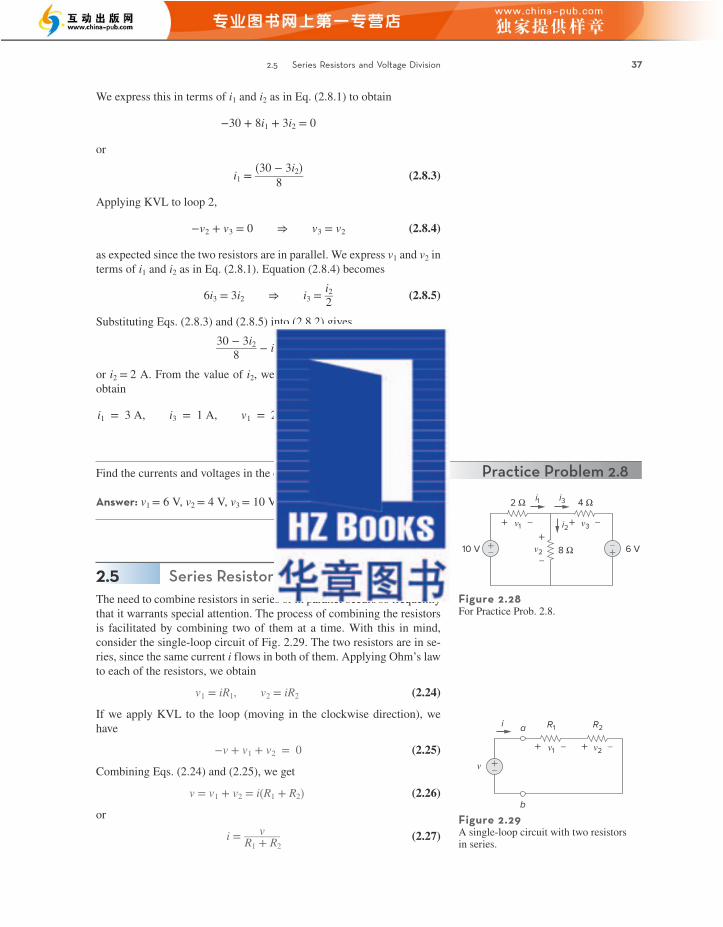
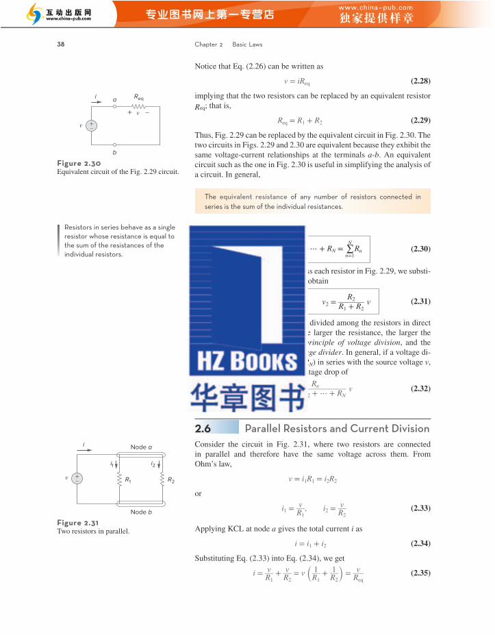
2.6 Parallel Resistors and Current Division 39
where Req is the equivalent resistance of the resistors in parallel:
1 ___ R eq = 1 __ R 1
+ 1 __ R 2 (2.36)
or
1 ___ Req
= R1 + R2 ______ R1R2
or
Req = R1R2 _____
R1 + R2 (2.37)
Thus,
The equivalent resistance of two parallel resistors is equal to the prod-uct of their resistances divided by their sum.
It must be emphasized that this applies only to two resistors in parallel. From Eq. (2.37), if R1 = R2 then Req = R1/R2.
We can extend the result in Eq. (2.36) to the general case of a circuit with N resistors in parallel. The equivalent resistance is
1 ___ R eq = 1 __ R 1
+ 1 __ R 2 + ⋯ + 1 ___ R N (2.38)
Note that Req is always smaller than the resistance of the smallest resistor in the parallel combination. If R1 = R2 = ⋯ = RN = R, then
R eq = R __ N
(2.39)
For example, if four 100-Ω resistors are connected in parallel, their equivalent resistance is 25 Ω.
It is often more convenient to use conductance rather than resistance when dealing with resistors in parallel. From Eq. (2.38), the equivalent conductance for N resistors in parallel is
G eq = G 1 + G 2 + G 3 + ⋯ + G N (2.40)
where Geq = 1/Req, G1 = 1/R1, G2 = 1/R2, G3 = 1/R3, … , GN = 1/RN. Equation (2.40) states:
The equivalent conductance of resistors connected in parallel is the sum of their individual conductances.
This means that we may replace the circuit in Fig. 2.31 with that in Fig. 2.32. Notice the similarity between Eqs. (2.30) and (2.40). The equivalent conductance of parallel resistors is obtained the same way as the equivalent resistance of series resistors. In the same manner, the equivalent conductance of resistors in series is obtained just the same
Conductances in parallel behave as a single conductance whose value is equal to the sum of the individual conductances.
Figure 2.32Equivalent circuit to Fig. 2.31.
b
a
v +– Req or Geqv
i
aLe26409_ch02_029-078.indd 45 9/27/19 2:30 PM
38 Chapter 2 Basic Laws
Notice that Eq. (2.26) can be written as
v = i R eq (2.28)
implying that the two resistors can be replaced by an equivalent resistor Req; that is,
R eq = R 1 + R 2 (2.29)
Thus, Fig. 2.29 can be replaced by the equivalent circuit in Fig. 2.30. The two circuits in Figs. 2.29 and 2.30 are equivalent because they exhibit the same voltage-current relationships at the terminals a-b. An equivalent circuit such as the one in Fig. 2.30 is useful in simplifying the analysis of a circuit. In general,
The equivalent resistance of any number of resistors connected in series is the sum of the individual resistances.
For N resistors in series then,
R eq = R 1 + R 2 + ⋯ + R N = ∑ n=1
N R n (2.30)
To determine the voltage across each resistor in Fig. 2.29, we substi-tute Eq. (2.26) into Eq. (2.24) and obtain
v 1 = R 1 _____ R 1 + R 2 v, v 2 = R 2 _____ R 1 + R 2
v (2.31)
Notice that the source voltage v is divided among the resistors in direct proportion to their resistances; the larger the resistance, the larger the voltage drop. This is called the principle of voltage division, and the circuit in Fig. 2.29 is called a voltage divider. In general, if a voltage di-vider has N resistors (R1, R2, … , RN) in series with the source voltage v, the nth resistor (Rn) will have a voltage drop of
v n = R n __________ R 1 + R 2 + ⋯ + R N v (2.32)
2.6 Parallel Resistors and Current DivisionConsider the circuit in Fig. 2.31, where two resistors are connected in parallel and therefore have the same voltage across them. From Ohm’s law,
v = i 1 R 1 = i 2 R 2
or
i 1 = v __ R 1 , i 2 = v __ R 2
(2.33)
Applying KCL at node a gives the total current i as
i = i 1 + i 2 (2.34)
Substituting Eq. (2.33) into Eq. (2.34), we get
i = v __ R 1 + v __ R 2
= v ( 1 __ R 1 + 1 __ R 2
) = v ___ R eq (2.35)
Figure 2.30Equivalent circuit of the Fig. 2.29 circuit.
v
Req
v+–
i
+ –
a
b
Resistors in series behave as a single resistor whose resistance is equal to the sum of the resistances of the individual resistors.
Figure 2.31Two resistors in parallel.
Node b
Node a
v +– R1 R2
i1 i2
i
aLe26409_ch02_029-078.indd 44 9/27/19 2:30 PM
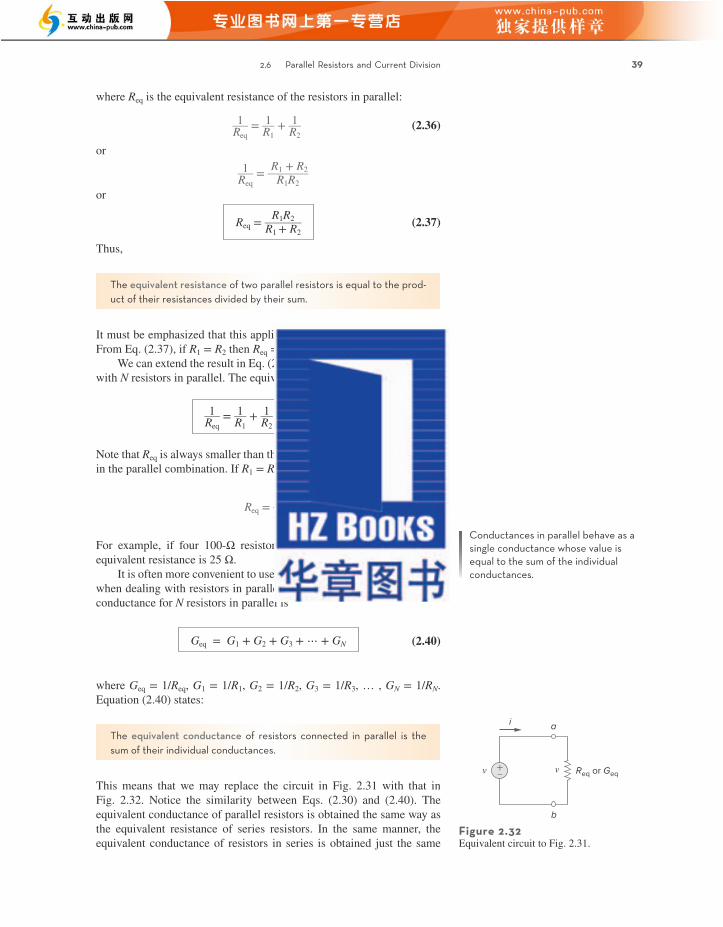
2.6 Parallel Resistors and Current Division 41
Example 2.9Find Req for the circuit shown in Fig. 2.34.
Solution:To get Req, we combine resistors in series and in parallel. The 6-Ω and 3-Ω resistors are in parallel, so their equivalent resistance is
6 Ω ∥ 3Ω = 6 × 3 ____ 6 + 3 = 2 Ω
(The symbol ∥ is used to indicate a parallel combination.) Also, the 1-Ω and 5-Ω resistors are in series; hence their equivalent resistance is
1 Ω + 5 Ω = 6 Ω
Thus the circuit in Fig. 2.34 is reduced to that in Fig. 2.35(a). In Fig. 2.35(a), we notice that the two 2-Ω resistors are in series, so the equivalent resistance is
2 Ω + 2 Ω = 4 Ω
This 4-Ω resistor is now in parallel with the 6-Ω resistor in Fig. 2.35(a); their equivalent resistance is
4 Ω ∥ 6 Ω = 4 × 6 ____ 4 + 6 = 2.4 Ω
The circuit in Fig. 2.35(a) is now replaced with that in Fig. 2.35(b). In Fig. 2.35(b), the three resistors are in series. Hence, the equivalent resis-tance for the circuit is
R eq = 4 Ω + 2.4 Ω + 8 Ω = 14.4 Ω
Figure 2.34For Example 2.9.
2 Ω5 ΩReq
4 Ω
8 Ω
1 Ω
6 Ω 3 Ω
6 ΩReq
4 Ω
(a)
8 Ω
2 Ω
2 Ω
2.4 ΩReq
4 Ω
(b)
8 Ω
Figure 2.35Equivalent circuits for Example 2.9.
Practice Problem 2.9By combining the resistors in Fig. 2.36, find Req.
Answer: 10 Ω.
Figure 2.36For Practice Prob. 2.9.
5 Ω4 Ω6 ΩReq
4 Ω
3 Ω
3 Ω 4 Ω
3 Ω
In general, it is often convenient and possible to combine resistors in series and parallel and reduce a resistive network to a single equivalent resistance Req. Such an equivalent resistance is the resistance between the designated terminals of the network and must exhibit the same i-v characteristics as the original network at the terminals.
aLe26409_ch02_029-078.indd 47 9/27/19 2:30 PM
40 Chapter 2 Basic Laws
way as the resistance of resistors in parallel. Thus, the equivalent con-ductance Geq of N resistors in series (such as shown in Fig. 2.29) is
1 ___ G eq = 1 __ G 1
+ 1 __ G 2 + 1 __ G 3
+ ⋯ + 1 ___ G N (2.41)
Given the total current i entering node a in Fig. 2.31, how do we obtain current i1 and i2? We know that the equivalent resistor has the same voltage, or
v = i R eq = i R 1 R 2 _____ R 1 + R 2 (2.42)
Combining Eqs. (2.33) and (2.42) results in
i 1 = R 2 i _____ R 1 + R 2 , i 2 = R 1 i _____ R 1 + R 2
(2.43)
which shows that the total current i is shared by the resistors in in-verse proportion to their resistances. This is known as the principle of current division, and the circuit in Fig. 2.31 is known as a current divider. Notice that the larger current flows through the smaller resistance.
As an extreme case, suppose one of the resistors in Fig. 2.31 is zero, say R2 = 0; that is, R2 is a short circuit, as shown in Fig. 2.33(a). From Eq. (2.43), R2 = 0 implies that i1 = 0, i2 = i. This means that the entire current i bypasses R1 and flows through the short circuit R2 = 0, the path of least resistance. Thus when a circuit is short circuited, as shown in Fig. 2.33(a), two things should be kept in mind:
1. The equivalent resistance Req = 0. [See what happens when R2 = 0 in Eq. (2.37).]
2. The entire current flows through the short circuit.
As another extreme case, suppose R2 = ∞, that is, R2 is an open circuit, as shown in Fig. 2.33(b). The current still flows through the path of least resistance, R1. By taking the limit of Eq. (2.37) as R 2 → ∞, we obtain Req = R1 in this case.
If we divide both the numerator and denominator by R1R2, Eq. (2.43) becomes
i 1 = G 1 _____ G 1 + G 2 i (2.44a)
i 2 = G 2 _____ G 1 + G 2 i (2.44b)
Thus, in general, if a current divider has N conductors (G1, G2, … , GN) in parallel with the source current i, the nth conductor (Gn) will have current
i n = G n __________ G 1 + G 2 + ⋯ + G N i (2.45)
R2 = 0
(a)
R1
i
i1 = 0 i2 = i
R2 = ∞
(b)
R1
i
i1 = i i2 = 0
Figure 2.33(a) A shorted circuit, (b) an open circuit.
aLe26409_ch02_029-078.indd 46 9/27/19 2:30 PM
2.6 Parallel Resistors and Current Division 43
Find the equivalent conductance Geq for the circuit in Fig. 2.40(a).
Solution:The 8-S and 12-S resistors are in parallel, so their conductance is
8 S + 12 S = 20 S
This 20-S resistor is now in series with 5 S as shown in Fig. 2.40(b) so that the combined conductance is
20 × 5 ____ 20 + 5 = 4 S
This is in parallel with the 6-S resistor. Hence,
G eq = 6 + 4 = 10 S
We should note that the circuit in Fig. 2.40(a) is the same as that in Fig. 2.40(c). While the resistors in Fig. 2.40(a) are expressed in siemens, those in Fig. 2.40(c) are expressed in ohms. To show that the circuits are the same, we find Req for the circuit in Fig. 2.40(c).
Req = 1 __ 6 ∥ ( 1 __ 5 + 1 __ 8 ∥ 1 ___ 12 ) = 1 __ 6 ∥ ( 1 __ 5 + 1 ___ 20 ) = 1 __ 6 ∥ 1 __ 4
= 1 _ 6 × 1 _ 4 ____ 1 _ 6 + 1 _ 4
= 1 ___ 10 Ω
Geq = 1 ___ Req
= 10 S
This is the same as we obtained previously.
Example 2.11
12 S8 S6 S
(a)
5 S
Geq
20 S6 S
(b)
5 S
Geq
(c)
Req
Ω15
Ω16 Ω1
8 Ω112
Figure 2.40For Example 2.11: (a) original circuit, (b) its equivalent circuit, (c) same circuit as in (a) but resistors are expressed in ohms.
Practice Problem 2.11Calculate Geq in the circuit of Fig. 2.41.
Answer: 4 S.
Figure 2.41For Practice Prob. 2.11.
4 S
4 S
8 S
2 S
Geq
Find io and vo in the circuit shown in Fig. 2.42(a). Calculate the power dissipated in the 3-Ω resistor.
Solution:The 6-Ω and 3-Ω resistors are in parallel, so their combined resistance is
6 Ω ∥ 3 Ω = 6 × 3 ____ 6 + 3 = 2 Ω
Thus, our circuit reduces to that shown in Fig. 2.42(b). Notice that vo is not affected by the combination of the resistors because the resistors are
Example 2.12
aLe26409_ch02_029-078.indd 49 9/27/19 2:30 PM
42 Chapter 2 Basic Laws
Calculate the equivalent resistance Rab in the circuit in Fig. 2.37.Example 2.10
Figure 2.37For Example 2.10.
a
bb b
c d
6 Ω
12 Ω
5 Ω4 Ω
10 Ω 1 Ω 1 Ω
Rab3 Ω
Solution:The 3-Ω and 6-Ω resistors are in parallel because they are connected to the same two nodes c and b. Their combined resistance is
3 Ω ∥ 6 Ω = 3 × 6 ____ 3 + 6 = 2 Ω (2.10.1)
Similarly, the 12-Ω and 4-Ω resistors are in parallel since they are con-nected to the same two nodes d and b. Hence
12 Ω ∥ 4 Ω = 12 × 4 ____ 12 + 4 = 3 Ω (2.10.2)
Also the 1-Ω and 5-Ω resistors are in series; hence, their equivalent resis-tance is
1 Ω + 5 Ω = 6 Ω (2.10.3)
With these three combinations, we can replace the circuit in Fig. 2.37 with that in Fig. 2.38(a). In Fig. 2.38(a), 3-Ω in parallel with 6-Ω gives 2-Ω, as calculated in Eq. (2.10.1). This 2-Ω equivalent resistance is now in series with the 1-Ω resistance to give a combined resistance of 1 Ω + 2 Ω = 3 Ω. Thus, we replace the circuit in Fig. 2.38(a) with that in Fig. 2.38(b). In Fig. 2.38(b), we combine the 2-Ω and 3-Ω resistors in parallel to get
2 Ω ∥ 3 Ω = 2 × 3 ____ 2 + 3 = 1.2 Ω
This 1.2-Ω resistor is in series with the 10-Ω resistor, so that
R ab = 10 + 1.2 = 11.2 Ω
(a)
bb
d
b
c
3 Ω 6 Ω2 Ω
10 Ω 1 Ωa
b
(b)
b b
c
3 Ω2 Ω
10 Ωa
b
Figure 2.38Equivalent circuits for Example 2.10.
Figure 2.39For Practice Prob. 2.10.
1 Ω9 Ω
18 Ω
20 Ω
20 Ω
2 Ω
5 Ω16 Ωa
b
Rab
Find Rab for the circuit in Fig. 2.39.
Answer: 19 Ω.
Practice Problem 2.10
aLe26409_ch02_029-078.indd 48 9/27/19 2:30 PM
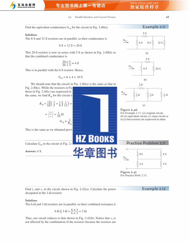
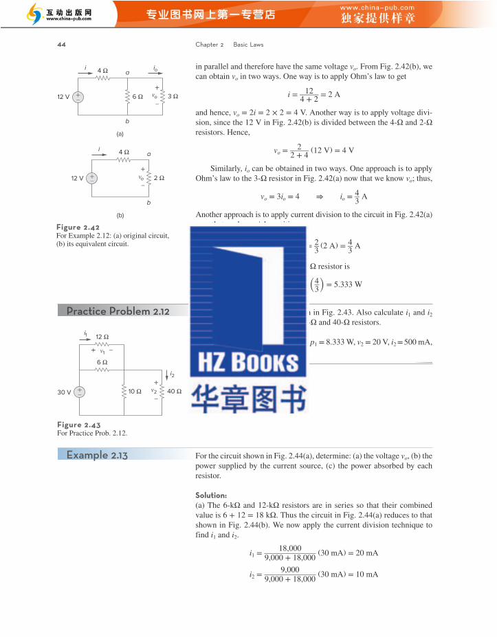
2.7 Wye-Delta Transformations 45
Notice that the voltage across the 9-kΩ and 18-kΩ resistors is the same, and vo = 9,000i1 = 18,000i2 = 180 V, as expected.(b) Power supplied by the source is
p o = v o i o = 180 (30) mW = 5.4 W
(c) Power absorbed by the 12-kΩ resistor is
p = iv = i 2 ( i 2 R) = i 2 2 R = (10 × 10−3)2 (12,000) = 1.2 W
Power absorbed by the 6-kΩ resistor is
p = i22 R = (10 × 10−3)2 (6,000) = 0.6 W
Power absorbed by the 9-kΩ resistor is
p = v 2 o __ R
= (180) 2 _____ 9,000 = 3.6 W
or
p = voi1 = 180(20) mW = 3.6 W
Notice that the power supplied (5.4 W) equals the power absorbed (1.2 + 0.6 + 3.6 = 5.4 W). This is one way of checking results.
(a)
30 mA 9 kΩvo
+
–12 kΩ
6 kΩ
(b)
30 mA 9 kΩvo
+
–18 kΩ
i1
io i2
Figure 2.44For Example 2.13: (a) original circuit, (b) its equivalent circuit.
Practice Problem 2.13For the circuit shown in Fig. 2.45, find: (a) v1 and v2, (b) the power dis-sipated in the 3-kΩ and 20-kΩ resistors, and (c) the power supplied by the current source.
30 mA3 kΩ 5 kΩ 20 kΩ
1 kΩ
v1
+
–v2
+
–
Figure 2.45For Practice Prob. 2.13.
Answer: (a) 45 V, 60 V, (b) 675 mW, 180 mW, (c) 1.8 W.
2.7 Wye-Delta TransformationsSituations often arise in circuit analysis when the resistors are neither in parallel nor in series. For example, consider the bridge circuit in Fig. 2.46. How do we combine resistors R1 through R6 when the resistors are nei-ther in series nor in parallel? Many circuits of the type shown in Fig. 2.46 can be simplified by using three-terminal equivalent networks. These are the wye (Y) or tee (T) network shown in Fig. 2.47 and the delta (Δ) or pi (Π) network shown in Fig. 2.48. These networks occur by themselves or as part of a larger network. They are used in three-phase networks, elec-trical filters, and matching networks. Our main interest here is in how to
vs+–
R1
R4
R2
R5
R3
R6
Figure 2.46The bridge network.
aLe26409_ch02_029-078.indd 51 9/27/19 2:30 PM
44 Chapter 2 Basic Laws
in parallel and therefore have the same voltage vo. From Fig. 2.42(b), we can obtain vo in two ways. One way is to apply Ohm’s law to get
i = 12 _____ 4 + 2 = 2 A
and hence, vo = 2i = 2 × 2 = 4 V. Another way is to apply voltage divi-sion, since the 12 V in Fig. 2.42(b) is divided between the 4-Ω and 2-Ω resistors. Hence,
v o = 2 _____ 2 + 4 (12 V) = 4 V
Similarly, io can be obtained in two ways. One approach is to apply Ohm’s law to the 3-Ω resistor in Fig. 2.42(a) now that we know vo; thus,
v o = 3 i o = 4 ⇒ i o = 4 __ 3 A
Another approach is to apply current division to the circuit in Fig. 2.42(a) now that we know i, by writing
i o = 6 _____ 6 + 3 i = 2 __ 3 (2 A) = 4 __ 3 A
The power dissipated in the 3-Ω resistor is
p o = voio = 4 ( 4 __ 3 ) = 5.333 W
a
b
(a)
12 V
4 Ωi io
6 Ω 3 Ωvo
+
–
a
b
(b)
12 V
4 Ωi
+– 2 Ωvo
+
–
+–
Figure 2.42For Example 2.12: (a) original circuit, (b) its equivalent circuit.
Find v1 and v2 in the circuit shown in Fig. 2.43. Also calculate i1 and i2 and the power dissipated in the 12-Ω and 40-Ω resistors.
Answer: v1 = 10 V, i1 = 833.3 mA, p1 = 8.333 W, v2 = 20 V, i2 = 500 mA, p2 = 10 W.
Practice Problem 2.12
Figure 2.43For Practice Prob. 2.12.
30 V
i1
+– 40 Ωv2
+
–10 Ω
12 Ω
v1
6 Ωi2
+ –
For the circuit shown in Fig. 2.44(a), determine: (a) the voltage vo, (b) the power supplied by the current source, (c) the power absorbed by each resistor.
Solution:(a) The 6-kΩ and 12-kΩ resistors are in series so that their combined value is 6 + 12 = 18 kΩ. Thus the circuit in Fig. 2.44(a) reduces to that shown in Fig. 2.44(b). We now apply the current division technique to find i1 and i2.
i 1 = 18,000 _____________ 9,000 + 18,000 (30 mA) = 20 mA
i 2 = 9,000 _____________ 9,000 + 18,000 (30 mA) = 10 mA
Example 2.13
aLe26409_ch02_029-078.indd 50 9/27/19 2:30 PM
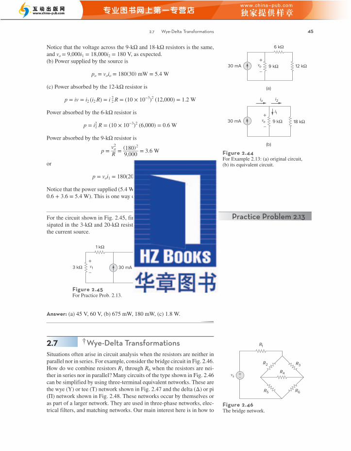
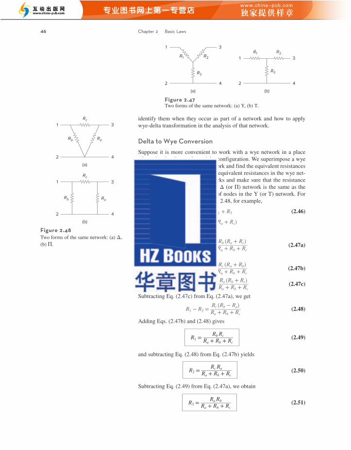
2.7 Wye-Delta Transformations 47
We do not need to memorize Eqs. (2.49) to (2.51). To transform a Δ network to Y, we create an extra node n as shown in Fig. 2.49 and follow this conversion rule:
Each resistor in the Y network is the product of the resistors in the two adjacent Δ branches, divided by the sum of the three Δ resistors.
One can follow this rule and obtain Eqs. (2.49) to (2.51) from Fig. 2.49.
Wye to Delta ConversionTo obtain the conversion formulas for transforming a wye network to an equivalent delta network, we note from Eqs. (2.49) to (2.51) that
R 1 R 2 + R 2 R 3 + R 3 R 1 = R a R b R c ( R a + R b + R c ) _________________ ( R a + R b + R c ) 2
(2.52) = R a R b R c _______ R a + R b + R c
Dividing Eq. (2.52) by each of Eqs. (2.49) to (2.51) leads to the follow-ing equations:
R a = R1 R2 + R2R3 + R3R1 _________________ R1
(2.53)
R b = R1 R2 + R2R3 + R3R1 _________________ R2
(2.54)
R c = R1 R2 + R2R3 + R3R1 _________________ R3
(2.55)
From Eqs. (2.53) to (2.55) and Fig. 2.49, the conversion rule for Y to Δ is as follows:
Each resistor in the Δ network is the sum of all possible products of Y resistors taken two at a time, divided by the opposite Y resistor.
The Y and Δ networks are said to be balanced when
R 1 = R 2 = R 3 = R Y , R a = R b = R c = R Δ (2.56)
Under these conditions, conversion formulas become
R Y = R Δ ___ 3 or R Δ = 3 R Y (2.57)
One may wonder why RY is less than RΔ. Well, we notice that the Y-connection is like a “series” connection while the Δ-connection is like a “parallel” connection.
Note that in making the transformation, we do not take anything out of the circuit or put in anything new. We are merely substituting different but mathematically equivalent three-terminal network patterns to create a circuit in which resistors are either in series or in parallel, allowing us to calculate Req if necessary.
Figure 2.49Superposition of Y and Δ networks as an aid in transforming one to the other.
R3
RaRb
R1 R2
Rc
b
n
a
c
aLe26409_ch02_029-078.indd 53 9/27/19 2:30 PM
46 Chapter 2 Basic Laws
identify them when they occur as part of a network and how to apply wye-delta transformation in the analysis of that network.
Delta to Wye ConversionSuppose it is more convenient to work with a wye network in a place where the circuit contains a delta configuration. We superimpose a wye network on the existing delta network and find the equivalent resistances in the wye network. To obtain the equivalent resistances in the wye net-work, we compare the two networks and make sure that the resistance between each pair of nodes in the Δ (or Π) network is the same as the resistance between the same pair of nodes in the Y (or T) network. For terminals 1 and 2 in Figs. 2.47 and 2.48, for example,
R 12 (Y) = R 1 + R 3 (2.46)
R12(Δ) = Rb ∥ (Ra + Rc)
Setting R12(Y) = R12(Δ) gives
R 12 = R 1 + R 3 = R b ( R a + R c ) _________ R a + R b + R c (2.47a)
Similarly,
R 13 = R 1 + R 2 = R c ( R a + R b ) _________ R a + R b + R c (2.47b)
R 34 = R 2 + R 3 = R a ( R b + R c ) _________ R a + R b + R c (2.47c)
Subtracting Eq. (2.47c) from Eq. (2.47a), we get
R 1 − R 2 = R c ( R b − R a ) _________ R a + R b + R c (2.48)
Adding Eqs. (2.47b) and (2.48) gives
R 1 = R b R c ________ R a + R b + R c (2.49)
and subtracting Eq. (2.48) from Eq. (2.47b) yields
R 2 = R c R a ________ R a + R b + R c (2.50)
Subtracting Eq. (2.49) from Eq. (2.47a), we obtain
R 3 = R a R b ________ R a + R b + R c (2.51)
1 3
2 4
R3
R2R1
(a)
1 3
2 4
R3
R2R1
(b)
Figure 2.47Two forms of the same network: (a) Y, (b) T.
Figure 2.48Two forms of the same network: (a) Δ, (b) Π.
1 3
2 4
Rc
(a)
1 3
2 4
(b)
RaRb
Rc
RaRb
aLe26409_ch02_029-078.indd 52 9/27/19 2:30 PM
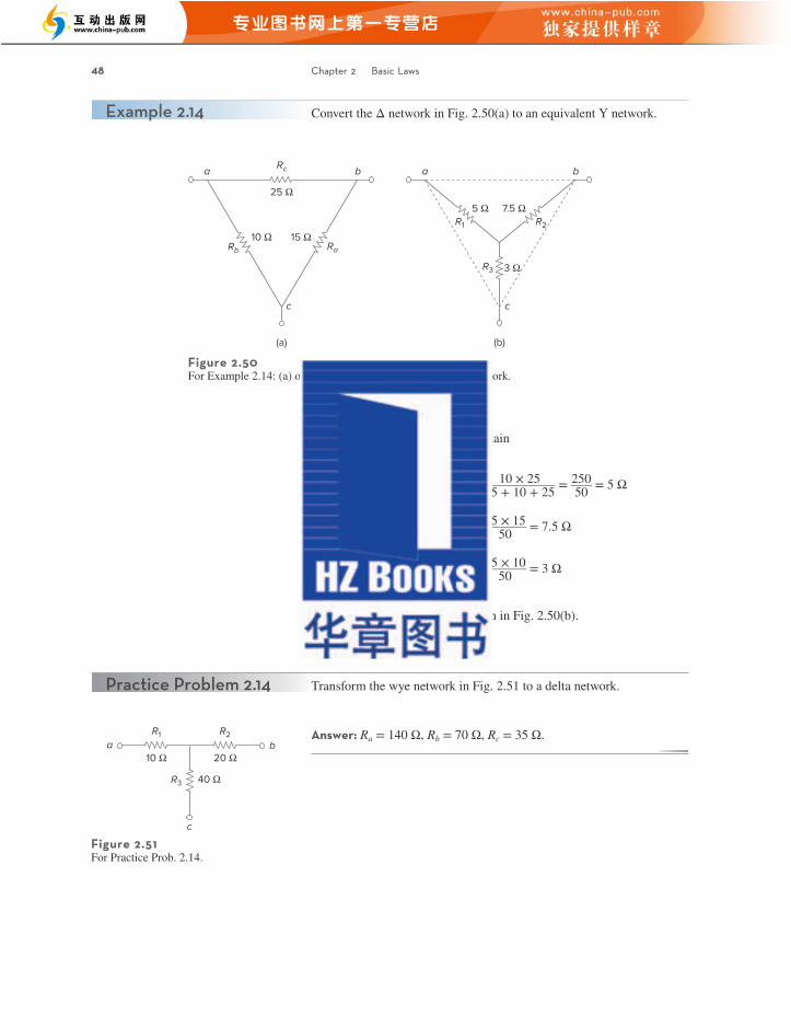
2.7 Wye-Delta Transformations 49
We can use wye-delta transformations as one approach to find a so-lution. It is useful to locate the wyes (there are two of them, one at n and the other at c) and the deltas (there are three: can, abn, cnb).
3. Alternative. There are different approaches that can be used to solve this problem. Since the focus of Sec. 2.7 is the wye-delta transfor-mation, this should be the technique to use. Another approach would be to solve for the equivalent resistance by injecting one amp into the circuit and finding the voltage between a and b; we will learn about this approach in Chap. 4.
The approach we can apply here as a check would be to use a wye-delta transformation as the first solution to the problem. Later we can check the solution by starting with a delta-wye transformation.
4. Attempt. In this circuit, there are two Y networks and three Δ networks. Transforming just one of these will simplify the circuit. If we convert the Y network comprising the 5-Ω, 10-Ω, and 20-Ω resistors, we may select
R 1 = 10 Ω, R 2 = 20 Ω, R 3 = 5 Ω
Thus from Eqs. (2.53) to (2.55) we have
R a = R 1 R 2 + R 2 R 3 + R 3 R 1 _____________ R 1 = 10 × 20 + 20 × 5 + 5 × 10 ______________ 10
= 350 ___ 10 = 35 Ω
R b = R 1 R 2 + R 2 R 3 + R 3 R 1 _____________ R 2 = 350 ___ 20 = 17.5 Ω
R
c
=
R 1 R 2 + R 2 R 3 + R 3 R 1
_____________
R
3
=
350
___
5
= 70 Ω
With the Y converted to Δ, the equivalent circuit (with the voltage source removed for now) is shown in Fig. 2.53(a). Combin-ing the three pairs of resistors in parallel, we obtain
70 ∥ 30 = 70 × 30 _____ 70 + 30 = 21 Ω
12.5 ∥ 17.5 = 12.5 × 17.5 ________ 12.5 + 17.5 = 7.292 Ω
15 ∥ 35 = 15 × 35 _____ 15 + 35 = 10.5 Ω
a ai
bb
c n120 V5 Ω
30 Ω
12.5 Ω
15 Ω
10 Ω
20 Ω
+–
Figure 2.52For Example 2.15.
aLe26409_ch02_029-078.indd 55 9/27/19 2:30 PM
Obtain the equivalent resistance Rab for the circuit in Fig. 2.52 and use it to find current i.
Solution:
1. Define. The problem is clearly defined. Please note, this part nor-mally will deservedly take much more time.
2. Present. Clearly, when we remove the voltage source, we end up with a purely resistive circuit. Since it is composed of deltas and wyes, we have a more complex process of combining the elements together.
Example 2.15
48 Chapter 2 Basic Laws
Convert the Δ network in Fig. 2.50(a) to an equivalent Y network.Example 2.14
Figure 2.50For Example 2.14: (a) original Δ network, (b) Y equivalent network.
c
ba
10 Ω 15 Ω
(a)
Rb Ra
Rc
25 Ω
c
ba
5 Ω
3 Ω
7.5 ΩR2R1
R3
(b)
Solution:Using Eqs. (2.49) to (2.51), we obtain
R 1 = R b R c _______ R a + R b + R c = 10 × 25 ________ 15 + 10 + 25 = 250 ___ 50 = 5 Ω
R 2 = R c R a _______ R a + R b + R c = 25 × 15 _____ 50 = 7.5 Ω
R 3 = R a R b _______ R a + R b + R c = 15 × 10 _____ 50 = 3 Ω
The equivalent Y network is shown in Fig. 2.50(b).
Practice Problem 2.14 Transform the wye network in Fig. 2.51 to a delta network.
Answer: Ra = 140 Ω, Rb = 70 Ω, Rc = 35 Ω.
Figure 2.51 For Practice Prob. 2.14.
20 Ω
R2
ba
c
10 Ω
R1
R3 40 Ω
aLe26409_ch02_029-078.indd 54 9/27/19 2:30 PM
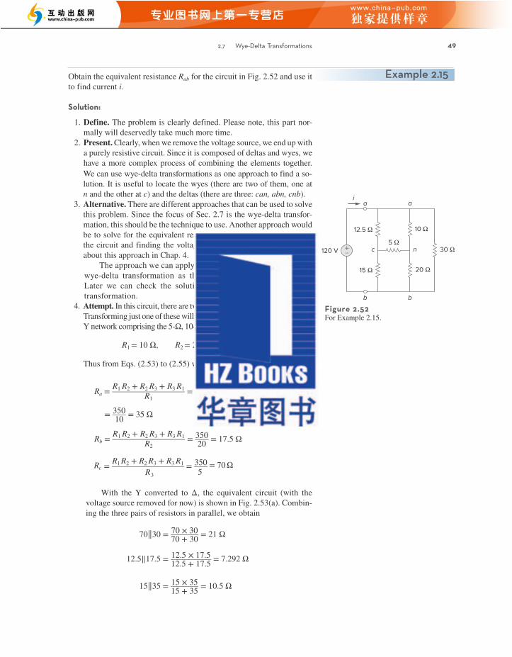
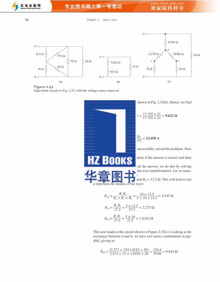
51
For the bridge network in Fig. 2.54, find Rab and i.
Answer: 40 Ω, 6 A.
Practice Problem 2.15
24 Ω
240 V
i
30 Ω
10 Ω
50 Ω
13 Ω
20 Ω+–
b
a
Figure 2.54For Practice Prob. 2.15.
aLe26409_ch02_029-078.indd 57 9/27/19 2:30 PM
Problems
Section 2.2 Ohm’s Law
2.1 Design a problem, complete with a solution, to help students to better understand Ohm’s law. Use at least two resistors and one voltage source. Hint, you could use both resistors at once or one at a time, it is up to you. Be creative.
2.2 Find the hot resistance of a light bulb rated 60 W, 120 V.
2.3 A bar of silicon is 4 cm long with a circular cross sec tion. If the resistance of the bar is 240 Ω at room tem perature, what is the cross-sectional radius of the bar?
This is in series with the 4.545-Ω resistor, both of which are in paral-lel with the 30-Ω resistor. This then gives us the equivalent resis-tance of the circuit.
R ab = (9.642 + 4.545) 30 ____________ 9.642 + 4.545 + 30 = 425.6 ____ 44.19 = 9.631 Ω
This now leads to
i = v s ___
R ab = 120 ____ 9.631 = 12.46 A
We note that using two variations on the wye-delta transformation leads to the same results. This represents a very good check.
6. Satisfactory? Since we have found the desired answer by deter-mining the equivalent resistance of the circuit first and the an-swer checks, then we clearly have a satisfactory solution. This represents what can be presented to the individual assigning the problem.
Problems 50 Chapter 2 Basic Laws
so that the equivalent circuit is shown in Fig. 2.53(b). Hence, we find
R ab = (7.292 + 10.5) ∥ 21 = 17.792 × 21 ________ 17.792 + 21 = 9.632 Ω
Then
i = v s ___ R ab = 120 ____ 9.632 = 12.458 A
We observe that we have successfully solved the problem. Now we must evaluate the solution.
5. Evaluate. Now we must determine if the answer is correct and then evaluate the final solution.
It is relatively easy to check the answer; we do this by solving the problem starting with a delta-wye transformation. Let us trans-form the delta, can, into a wye.
Let Rc = 10 Ω, Ra = 5 Ω, and Rn = 12.5 Ω. This will lead to (let d represent the middle of the wye):
R ad = R c R n _______
R a + R c + R n = 10 × 12.5 ________ 5 + 10 + 12.5 = 4.545 Ω
R cd = R a R n ____ 27.5 = 5 × 12.5 ______ 27.5 = 2.273 Ω
R nd = R a R c ____ 27.5 = 5 × 10 ____ 27.5 = 1.8182 Ω
This now leads to the circuit shown in Figure 2.53(c). Looking at the resistance between d and b, we have two series combination in par-allel, giving us
R db = (2.273 + 15) (1.8182 + 20) ________________ 2.273 + 15 + 1.8182 + 20 = 376.9 ____ 39.09 = 9.642 Ω
aLe26409_ch02_029-078.indd 56 9/27/19 2:30 PM
a
b
30 Ω70 Ω
17.5 Ω
35 Ω
12.5 Ω
15 Ω
(a)
a
b
21 Ω
(b)
7.292 Ω
10.5 Ω
a
b
c n
d
30 Ω
4.545 Ω
20 Ω
1.8182 Ω2.273 Ω
15 Ω
(c)
Figure 2.53Equivalent circuits to Fig. 2.52, with the voltage source removed.
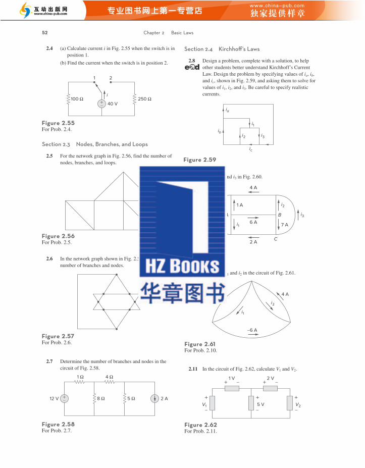
Problems 53
2.12 In the circuit in Fig. 2.63, obtain v1, v2, and v3.
2.13 For the circuit in Fig. 2.64, use KCL to find the branch currents I1 to I4.
2.14 Given the circuit in Fig. 2.65, use KVL to find the branch voltages V1 to V4.
2.15 Calculate v and ix in the circuit of Fig. 2.66.
2.16 Determine Vo in the circuit in Fig. 2.67.
2.17 Obtain v1 through v3 in the circuit of Fig. 2.68.
2.18 Find I and Vab in the circuit of Fig. 2.69.
2.19 From the circuit in Fig. 2.70, find I, the power dissipated by the resistor, and the power supplied by each source.
40 V
– 50 V + + 20 V – + v2 –
+v1–
+v3–
+ 30 V –
+
–
Figure 2.63For Prob. 2.12.
I1
I2 I4
I3
7 A
2 A
4 A3 A
Figure 2.64For Prob. 2.13.
V2
V4
V1
V3
3 V
4 V 5 V
+
–
– –
+
+
–
–
2 V
+ +
++ –
–
+ –
Figure 2.65For Prob. 2.14.
Figure 2.66For Prob. 2.15.
ix
3ix10 V +–
+ 16 V –
+ 4 V
–
+ v –
12 Ω
+–
10 V 25 V+– +–
14 Ω
+
Vo
–
16 Ω
Figure 2.67For Prob. 2.16.
24 V
12 V
10 Vv3v2+–
+–
+–
+
–+–
v1+ –
Figure 2.68For Prob. 2.17.
+
–30 V
I
8 V
10 V3 Ω 5 Ω
+–
+–
+–
Vab
b
a
Figure 2.69For Prob. 2.18.
12 V
10 V
–8 V
3 Ω+–
+ –
+ –
I
Figure 2.70For Prob. 2.19.
aLe26409_ch02_029-078.indd 67 9/27/19 2:30 PM
52 Chapter 2 Basic Laws
2.4 (a) Calculate current i in Fig. 2.55 when the switch is in position 1.
(b) Find the current when the switch is in position 2.
Section 2.3 Nodes, Branches, and Loops
2.5 For the network graph in Fig. 2.56, find the number of nodes, branches, and loops.
2.6 In the network graph shown in Fig. 2.57, determine the number of branches and nodes.
2.7 Determine the number of branches and nodes in the circuit of Fig. 2.58.
Section 2.4 Kirchhoff’s Laws
2.8 Design a problem, complete with a solution, to help other students better understand Kirchhoff’s Current Law. Design the problem by specifying values of ia, ib, and ic, shown in Fig. 2.59, and asking them to solve for values of i1, i2, and i3. Be careful to specify realistic currents.
2.9 Find i1, i2, and i3 in Fig. 2.60.
2.10 Determine i1 and i2 in the circuit of Fig. 2.61.
2.11 In the circuit of Fig. 2.62, calculate V1 and V2.
250 Ω100 Ω40 V
1 2
i
+–
Figure 2.55For Prob. 2.4.
Figure 2.56For Prob. 2.5.
Figure 2.57For Prob. 2.6.
12 V 2 A
1 Ω 4 Ω
8 Ω 5 Ω+–
Figure 2.58For Prob. 2.7.
Figure 2.60For Prob. 2.9.
5 A
2 A
4 A
1 A
A B
C
7 Ai1
i3
i2
6 A
Figure 2.61For Prob. 2.10.
–6 A
–8 A 4 A
i2
i1
5 V
+
––
+
–
+
+ –1 V
+ –2 V
V1 V2
Figure 2.62For Prob. 2.11.
Figure 2.59For Prob. 2.8.
ia
ic
ib
i1
i3i2
aLe26409_ch02_029-078.indd 66 9/27/19 2:30 PM
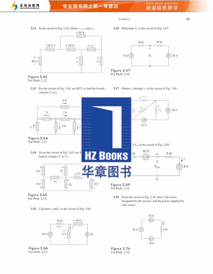
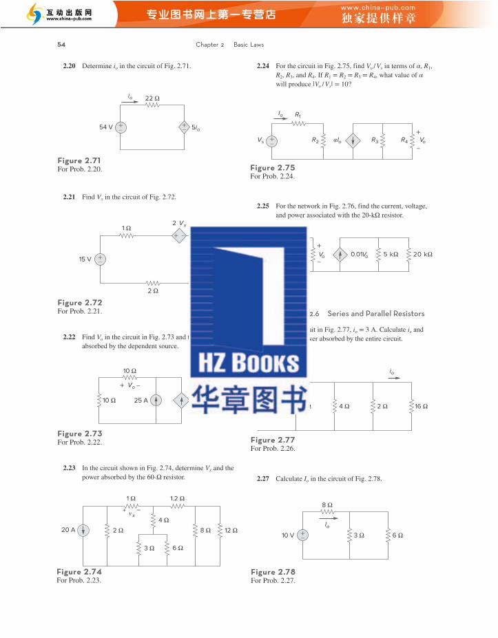
Problems 55
2.28 Design a problem, using Fig. 2.79, to help other students better understand series and parallel circuits.
2.32 Find i1 through i4 in the circuit in Fig. 2.83.
Vs
R1
R2
v1
v2+–
+ –+
–R3
v3
+
–
Figure 2.79For Prob. 2.28.
2.29 All resistors (R) in Fig. 2.80 are 5 Ω each. Find Req.
Req
RR R
RRR
Figure 2.80For Prob. 2.29.
2.30 Find Req for the circuit in Fig. 2.81.
60 Ω
180 Ω25 Ω
60 Ω
Req
Figure 2.81For Prob. 2.30.
2.31 For the circuit in Fig. 2.82, determine i1 to i5.
200 V1 Ω 2 Ω
4 Ω+–
3 Ω
i2
i1
i4 i5
i3
Figure 2.82For Prob. 2.31.
i4 i2
i3 i1
40 Ω
60 Ω
50 Ω
200 Ω
16 A
Figure 2.83For Prob. 2.32.
2.33 Obtain v and i in the circuit of Fig. 2.84.
9 A 2 S1 S
4 S 6 S
3 S+
–v
i
Figure 2.84For Prob. 2.33.
2.34 Using series/parallel resistance combination, find the equivalent resistance seen by the source in the circuit of Fig. 2.85. Find the overall absorbed power by the resistor network.
160 Ω200 V
20 Ω 28 Ω
160 Ω 80 Ω
60 Ω
52 Ω 20 Ω
–+
Figure 2.85For Prob. 2.34.
2.35 Calculate Vo and Io in the circuit of Fig. 2.86.
200 V
30 Ω70 Ω
+–
5 Ω20 Ω+
–Vo
Io
Figure 2.86For Prob. 2.35.
aLe26409_ch02_029-078.indd 69 9/27/19 2:30 PM
54 Chapter 2 Basic Laws
2.20 Determine io in the circuit of Fig. 2.71.
2.21 Find Vx in the circuit of Fig. 2.72.
2.22 Find Vo in the circuit in Fig. 2.73 and the power absorbed by the dependent source.
2.23 In the circuit shown in Fig. 2.74, determine Vx and the power absorbed by the 60-Ω resistor.
2.24 For the circuit in Fig. 2.75, find Vo / Vs in terms of α, R1, R2, R3, and R4. If R1 = R2 = R3 = R4, what value of α will produce |Vo / Vs| = 10?
2.25 For the network in Fig. 2.76, find the current, voltage, and power associated with the 20-kΩ resistor.
Sections 2.5 and 2.6 Series and Parallel Resistors
2.26 For the circuit in Fig. 2.77, io = 3 A. Calculate ix and the total power absorbed by the entire circuit.
2.27 Calculate Io in the circuit of Fig. 2.78.
Figure 2.71For Prob. 2.20.
54 V
22 Ω
+– 5io+–
io
+
–15 V +–
1 Ω
2 Ω
5 Ω Vx
+ –
2 Vx
Figure 2.72For Prob. 2.21.
Figure 2.73For Prob. 2.22.
2 Vo25 A
10 Ω
10 Ω
+ Vo –
20 A 2 Ω4 Ω
3 Ω 6 Ω
8 Ω 12 Ω
1.2 Ω1 Ω
vx+ –
Figure 2.74For Prob. 2.23.
Vo+–
+
–R4R3
R1
R2 IoVs
Io
Figure 2.75For Prob. 2.24.
0.01VoVo
+
–20 kΩ5 kΩ10 kΩ5 mA
Figure 2.76For Prob. 2.25.
ix io10 Ω
8 Ω 4 Ω 2 Ω 16 Ω
Figure 2.77For Prob. 2.26.
Figure 2.78For Prob. 2.27.
Io
8 Ω
3 Ω 6 Ω10 V +–
aLe26409_ch02_029-078.indd 68 9/27/19 2:30 PM
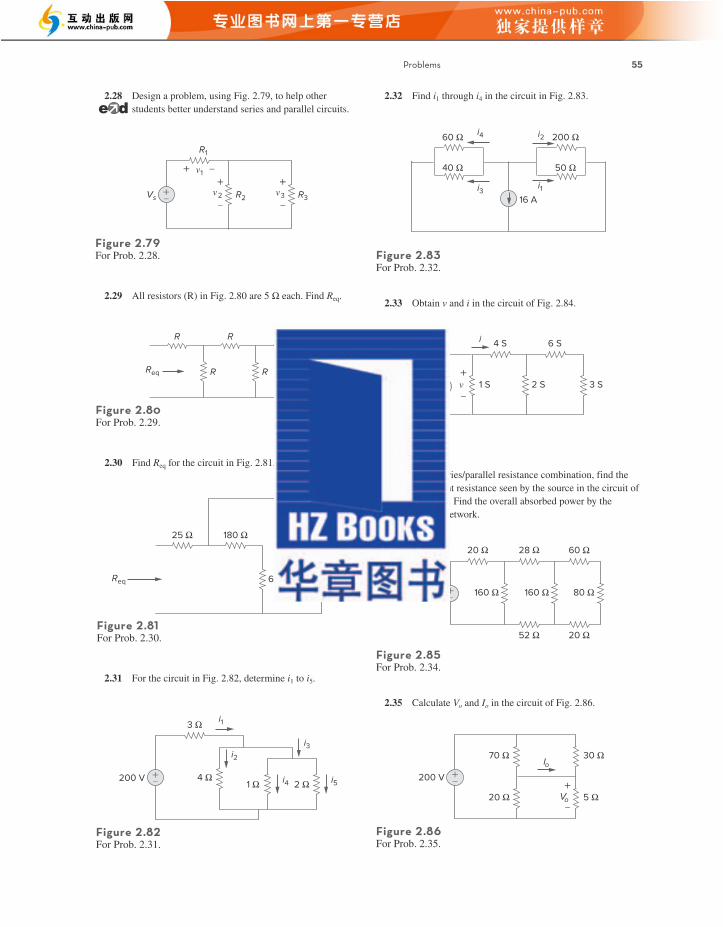
Problems 57
2.45 Find the equivalent resistance at terminals a-b of each circuit in Fig. 2.96.
2.43 Calculate the equivalent resistance Rab at terminals a-b for each of the circuits in Fig. 2.94.
8 Ω
5 Ω
20 Ω
30 Ω
a b
(a)
5 Ω
4 Ω
8 Ω
5 Ω
10 Ω
4 Ω
2 Ω
3 Ω
a b
(b)
Figure 2.93For Prob. 2.42.
40 Ω10 Ω
5 Ω
20 Ω
(a)
a
b
30 Ω80 Ω
60 Ω
(b)
a
b
10 Ω
20 Ω
Figure 2.94For Prob. 2.43.
2.44 For the circuits in Fig. 2.95, obtain the equivalent resistance at terminals a-b.
20 Ωa
b
5 Ω
2 Ω 3 Ω
Figure 2.95For Prob. 2.44.
10 Ω
40 Ω
20 Ω
30 Ω
50 Ω
(a)
5 Ω
a
b
(b)
5 Ω 20 Ω
25 Ω 60 Ω
12 Ω
15 Ω 10 Ω
30 Ω
Figure 2.96For Prob. 2.45.
2.46 Find I in the circuit of Fig. 2.97.
20 Ω
5 Ω
5 Ω
24 Ω
8 Ω
15 Ω
15 Ω
15 Ω
I
12 Ω
80 V –+
Figure 2.97For Prob. 2.46.
aLe26409_ch02_029-078.indd 71 9/27/19 2:30 PM
56 Chapter 2 Basic Laws
2.40 For the ladder network in Fig. 2.91, find I and Req.
2.36 Find i and Vo in the circuit of Fig. 2.87.
25 Ω
80 Ω 24 Ω 50 Ω
20 Ω
60 Ω 20 Ω
30 Ω20 V +–
i
–
+Vo
Figure 2.87For Prob. 2.36.
2.37 Find R for the circuit in Fig. 2.88.
R
20 V 30 V+–
–+
10 Ω
Figure 2.88For Prob. 2.37.
2.38 Find Req and io in the circuit of Fig. 2.89.
6 Ω
60 Ω
15 Ω 20 Ω
80 Ω
io 2.5 Ω
35 V +–
Req
12 Ω
Figure 2.89For Prob. 2.38.
2.39 Evaluate Req looking into each set of terminals for each of the circuits shown in Fig. 2.90.
2 kΩ1 kΩ
1 kΩ2 kΩ
(a)
12 kΩ4 kΩ
6 kΩ
12 kΩ
(b)
Figure 2.90For Prob. 2.39.
15 V 6 Ω
2 Ω
+–
8 Ω 1 Ω
2 Ω4 Ω
I
Req
Figure 2.91For Prob. 2.40.
2.41 If Req = 50 Ω in the circuit of Fig. 2.92, find R.
Req
30 Ω10 Ω
60 Ω
R
12 Ω 12 Ω 12 Ω
Figure 2.92For Prob. 2.41.
2.42 Reduce each of the circuits in Fig. 2.93 to a single resistor at terminals a-b.
8 Ω
5 Ω
20 Ω
30 Ω
a b
(a)
5 Ω
4 Ω
8 Ω
5 Ω
10 Ω
4 Ω
2 Ω
3 Ω
a b
(b)aLe26409_ch02_029-078.indd 70 9/27/19 2:30 PM
Problems 59
2.56 Determine V in the circuit of Fig. 2.107.2.53 Obtain the equivalent resistance Rab in each of the circuits of Fig. 2.104. In (b), all resistors have a value of 30 Ω.
*
(b)
40 Ω
50 Ω
10 Ω
60 Ω
30 Ω
20 Ω
(a)
b
a
80 Ω
30 Ωa
b
Figure 2.104For Prob. 2.53.
2.54 Consider the circuit in Fig. 2.105. Find the equivalent resistance at terminals: (a) a-b, (b) c-d.
50 Ω
60 Ω
100 Ω
150 Ω
150 Ω
100 Ω
a c
db
Figure 2.105For Prob. 2.54.
2.55 Calculate Io in the circuit of Fig. 2.106.
20 Ω
40 Ω
60 Ω
50 Ω10 Ω
20 Ω
24 V +–
Io
Figure 2.106For Prob. 2.55.
100 V
30 Ω
15 Ω 10 Ω16 Ω
35 Ω 12 Ω 20 Ω+– V+
–
Figure 2.107For Prob. 2.56.
2.57 Find Req and I in the circuit of Fig. 2.108.*
2 Ω4 Ω
12 Ω6 Ω 1 Ω
8 Ω 2 Ω
3 Ω10 Ω5 Ω
4 Ω20 V +–
Req
I
Figure 2.108For Prob. 2.57.
aLe26409_ch02_029-078.indd 73 9/27/19 2:30 PM
58 Chapter 2 Basic Laws
2.47 Find the equivalent resistance Rab in the circuit of Fig. 2.98.
ad e
f
b
c
6 Ω
3 Ω
5 Ω
20 Ω
10 Ω 8 Ω
Figure 2.98For Prob. 2.47.
Section 2.7 Wye-Delta Transformations
2.48 Convert the circuits in Fig. 2.99 from Y to Δ.
10 Ω 10 Ω
10 Ω
ba
c
(a)
20 Ω30 Ω
50 Ω
a
(b)
b
c
Figure 2.99For Prob. 2.48.
2.49 Transform the circuits in Fig. 2.100 from Δ to Y.
12 Ω
12 Ω 12 Ω
(a)
a b
c
60 Ω
30 Ω 10 Ω
(b)
a b
c
Figure 2.100For Prob. 2.49.
2.50 Design a problem to help other students better understand wye-delta transformations using Fig. 2.101.
9 mA
R R
R
R
R
Figure 2.101For Prob. 2.50.
2.51 Obtain the equivalent resistance at the terminals a-b for each of the circuits in Fig. 2.102.
(a)
b
a
30 Ω
10 Ω10 Ω
20 Ω
20 Ω10 Ω
20 Ω10 Ω
30 Ω
25 Ω
(b)
b
a
15 Ω5 Ω
Figure 2.102For Prob. 2.51.
2.52 For the circuit shown in Fig. 2.103, find the equivalent resistance. All resistors are 3Ω.
*
Req
Figure 2.103For Prob. 2.52.
* An asterisk indicates a challenging problem.
aLe26409_ch02_029-078.indd 72 9/27/19 2:30 PM

61
Methods of AnalysisNo great work is ever done in a hurry. To develop a great scientific dis-covery, to print a great picture, to write an immortal poem, to become a minister, or a famous general—to do anything great requires time, pa-tience, and perseverance. These things are done by degrees, “little by little.”
—W. J. Wilmont Buxton
c h a p t e r
3
Enhancing Your Career
Career in ElectronicsOne area of application for electric circuit analysis is electronics. The term electronics was originally used to distinguish circuits of very low current levels. This distinction no longer holds, as power semiconductor devices operate at high levels of current. Today, electronics is regarded as the science of the motion of charges in a gas, vacuum, or semiconduc-tor. Modern electronics involves transistors and transistor circuits. The earlier electronic circuits were assembled from components. Many elec-tronic circuits are now produced as integrated circuits, fabricated in a semiconductor substrate or chip.
Electronic circuits find applications in many areas, such as automa-tion, broadcasting, computers, and instrumentation. The range of devices that use electronic circuits is enormous and is limited only by our imag-ination. Radio, television, computers, and stereo systems are but a few.
An electrical engineer usually performs diverse functions and is likely to use, design, or construct systems that incorporate some form of elec-tronic circuits. Therefore, an understanding of the operation and analysis of electronics is essential to the electrical engineer. Electronics has become a specialty distinct from other disciplines within electrical engineering. Because the field of electronics is ever advancing, an electronics engineer must update his/her knowledge from time to time. The best way to do this is by being a member of a professional organization such as the Institute of Electrical and Electronics Engineers (IEEE). With a membership of over 300,000, the IEEE is the largest professional organization in the world. Members benefit immensely from the numerous magazines, jour-nals, transactions, and conference/symposium proceedings published yearly by IEEE. You should consider becoming an IEEE member.
Troubleshooting an electronic circuit board.Steve Allen/Stockbyte/Getty Images
aLe26409_ch03_079-124.indd 79 9/27/19 1:29 PM
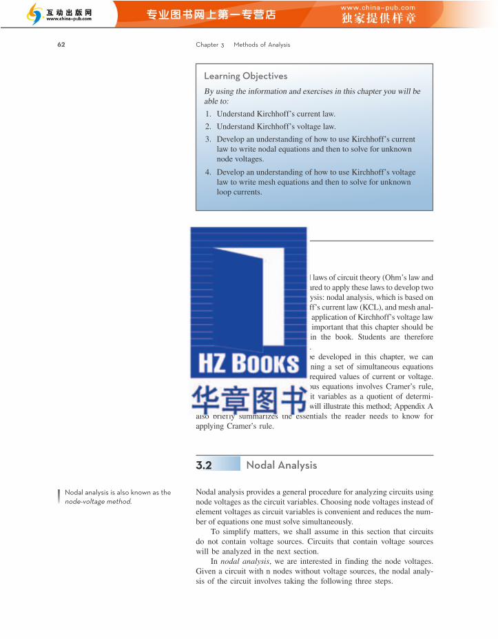
3.2 Nodal Analysis 63
The number of nonreference nodes is equal to the number of independent equations that we will derive.
Figure 3.1Common symbols for indicating a reference node, (a) common ground, (b) ground, (c) chassis ground.
(a) (b) (c)
Current flows from a higher potential to a lower potential in a resistor.
We shall now explain and apply these three steps.The first step in nodal analysis is selecting a node as the reference
or datum node. The reference node is commonly called the ground since it is assumed to have zero potential. A reference node is indicated by any of the three symbols in Fig. 3.1. The type of ground in Fig. 3.1(c) is called a chassis ground and is used in devices where the case, enclo-sure, or chassis acts as a reference point for all circuits. When the potential of the earth is used as reference, we use the earth ground in Fig. 3.1(a) or (b). We shall always use the symbol in Fig. 3.1(b).
Once we have selected a reference node, we assign voltage desig-nations to nonreference nodes. Consider, for example, the circuit in Fig. 3.2(a). Node 0 is the reference node (v = 0), while nodes 1 and 2 are assigned voltages v1 and v2, respectively. Keep in mind that the node voltages are defined with respect to the reference node. As illus-trated in Fig. 3.2(a), each node voltage is the voltage rise from the reference node to the corresponding nonreference node or simply the voltage of that node with respect to the reference node.
As the second step, we apply KCL to each nonreference node in the circuit. To avoid putting too much information on the same circuit, the circuit in Fig. 3.2(a) is redrawn in Fig. 3.2(b), where we now add i1, i2, and i3 as the currents through resistors R1, R2, and R3, respectively. At node 1, applying KCL gives
I1 = I2 + i1 + i2 (3.1)
At node 2,
I2 + i2 = i3 (3.2)
We now apply Ohm’s law to express the unknown currents i1, i2, and i3 in terms of node voltages. The key idea to bear in mind is that, since resis-tance is a passive element, by the passive sign convention, current must always flow from a higher potential to a lower potential.
Figure 3.2Typical circuit for nodal analysis.
(a)
(b)
1 2
v1
i1
i2 i2
i3
v2
I2
0
R3v2
+
–
R3
R1v1
+
–
R1I1
I2
R2
R2
I1
We can express this principle as
i = vhigher − vlower ___________
R (3.3)
Steps to Determine Node Voltages:1. Select a node as the reference node. Assign voltages v1, v2, . . . ,
vn − 1 to the remaining n − 1 nodes. The voltages are referenced with respect to the reference node.
2. Apply KCL to each of the n − 1 nonreference nodes. Use Ohm’s law to express the branch currents in terms of node voltages.
3. Solve the resulting simultaneous equations to obtain the un-known node voltages.
aLe26409_ch03_079-124.indd 81 9/27/19 1:29 PM
3.1 Introduction
Having understood the fundamental laws of circuit theory (Ohm’s law and Kirchhoff’s laws), we are now prepared to apply these laws to develop two powerful techniques for circuit analysis: nodal analysis, which is based on a systematic application of Kirchhoff’s current law (KCL), and mesh anal-ysis, which is based on a systematic application of Kirchhoff’s voltage law (KVL). The two techniques are so important that this chapter should be regarded as the most important in the book. Students are therefore encouraged to pay careful attention.
With the two techniques to be developed in this chapter, we can analyze any linear circuit by obtaining a set of simultaneous equations that are then solved to obtain the required values of current or voltage. One method of solving simultaneous equations involves Cramer’s rule, which allows us to calculate circuit variables as a quotient of determi-nants. The examples in the chapter will illustrate this method; Appendix A also briefly summarizes the essentials the reader needs to know for
3.2 Nodal Analysis
Nodal analysis provides a general procedure for analyzing circuits using node voltages as the circuit variables. Choosing node voltages instead of element voltages as circuit variables is convenient and reduces the num-ber of equations one must solve simultaneously.
To simplify matters, we shall assume in this section that circuits do not contain voltage sources. Circuits that contain voltage sources will be analyzed in the next section.
In nodal analysis, we are interested in finding the node voltages. Given a circuit with n nodes without voltage sources, the nodal analy-sis of the circuit involves taking the following three steps.
62 Chapter 3 Methods of Analysis
Nodal analysis is also known as the node-voltage method.
Learning ObjectivesBy using the information and exercises in this chapter you will be able to:1. Understand Kirchhoff’s current law.2. Understand Kirchhoff’s voltage law.3. Develop an understanding of how to use Kirchhoff’s current
law to write nodal equations and then to solve for unknown node voltages.
4. Develop an understanding of how to use Kirchhoff’s voltage law to write mesh equations and then to solve for unknown loop currents.
aLe26409_ch03_079-124.indd 80 9/27/19 1:29 PM
applying Cramer’s rule.
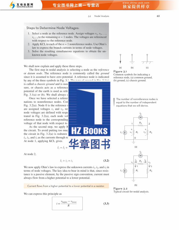
3.2 Nodal Analysis 65
or 3v1 − v2 = 20 (3.1.1)
At node 2, we do the same thing and get
i2 + i4 = i1 + i5 ⇒ v1 − v2 ______ 4 + 10 = 5 + v2 − 0 ______
6
Multiplying each term by 12 results in
3v1 − 3v2 + 120 = 60 + 2v2
or −3v1 + 5v2 = 60 (3.1.2)
Now we have two simultaneous Eqs. (3.1.1) and (3.1.2). We can solve the equations using any method and obtain the values of v1 and v2.
METHOD 1 Using the elimination technique, we add Eqs. (3.1.1) and (3.1.2).
4v2 = 80 ⇒ v2 = 20 V
Substituting v2 = 20 in Eq. (3.1.1) gives
3v1 − 20 = 20 ⇒ v1 = 40 ___ 3 = 13.333 V
METHOD 2 To use Cramer’s rule, we need to put Eqs. (3.1.1) and (3.1.2) in matrix form as
[ 3 −3
−1 5 ] [ v1 v2
] = [ 20 60
] (3.1.3)
The determinant of the matrix is
Δ = [ 3 −3
−1 5 ] = 15 − 3 = 12
We now obtain v1 and v2 as
v1 = Δ1 ___ Δ
= ǀ 20 60
−1 5 ǀ ________
Δ = 100 + 60 ________
12 = 13.333 V
v2 = Δ2 ___ Δ
= ǀ 3 −3
20 60
ǀ ________ Δ
= 180 + 60 ________ 12
= 20 V
giving us the same result as did the elimination method.
If we need the currents, we can easily calculate them from the values of the nodal voltages.
i1 = 5 A, i2 = v1 − v2 ______ 4 = −1.6668 A, i3 = v1 __
2 = 6.666 A
i4 = 10 A, i5 = v2 __ 6 = 3.333 A
The fact that i2 is negative shows that the current flows in the direction opposite to the one assumed.
Figure 3.3For Example 3.1: (a) original circuit, (b) circuit for analysis.
21
5 A
10 A2 Ω 6 Ω
4 Ω
(a)
5 A
10 A2 Ω 6 Ω
4 Ω
(b)
i1 = 5 i1 = 5
i4 = 10i2
i3i2 i5
v2v1
Practice Problem 3.1Obtain the node voltages in the circuit of Fig. 3.4.
Answer: v1 = −6 V, v2 = −42 V.
aLe26409_ch03_079-124.indd 83 9/27/19 1:29 PM
Note that this principle is in agreement with the way we defined resis-tance in Chapter 2 (see Fig. 2.1). With this in mind, we obtain from Fig. 3.2(b), i1 = v1 − 0 ______
R1 or i1 = G1v1
i2 = v1 − v2 ______ R2
or i2 = G2 (v1 − v2) (3.4)
i3 = v2 − 0 ______ R3
or i3 = G3v2
Substituting Eq. (3.4) in Eqs. (3.1) and (3.2) results, respectively, in
I1 = I2 + v1 ___ R1
+ v1 − v2 ______ R2
(3.5)
I2 + v1 − v2 ______ R2
= v2 ___ R3
(3.6)
In terms of the conductances, Eqs. (3.5) and (3.6) become
I1 = I2 + G1v1 + G2(v1 − v2) (3.7)
I2 + G2(v1 − v2) = G3v2 (3.8)
The third step in nodal analysis is to solve for the node voltages. If we apply KCL to n − 1 nonreference nodes, we obtain n − 1 simul-taneous equations such as Eqs. (3.5) and (3.6) or (3.7) and (3.8). For the circuit of Fig. 3.2, we solve Eqs. (3.5) and (3.6) or (3.7) and (3.8) to obtain the node voltages v1 and v2 using any standard method, such as the substitution method, the elimination method, Cramer’s rule, or matrix inversion. To use either of the last two methods, one must cast the simultaneous equations in matrix form. For example, Eqs. (3.7) and (3.8) can be cast in matrix form as
[ G1 + G2
−G2 −G2
G2 + G3 ] [ v1
v2 ] = [ I1 − I2
I2 ] (3.9)
which can be solved to get v1 and v2. Equation 3.9 will be generalized in Section 3.6. The simultaneous equations may also be solved using calcu-lators or with software packages such as MATLAB, Mathcad, Maple, and Quattro Pro.
64 Chapter 3 Methods of Analysis
Appendix A discusses how to use Cramer’s rule.
Example 3.1 Calculate the node voltages in the circuit shown in Fig. 3.3(a).
Solution:Consider Fig. 3.3(b), where the circuit in Fig. 3.3(a) has been prepared for nodal analysis. Notice how the currents are selected for the application of KCL. Except for the branches with current sources, the labeling of the currents is arbitrary but consistent. (By consistent, we mean that if, for example, we assume that i2 enters the 4-Ω resistor from the left-hand side, i2 must leave the resistor from the right-hand side.) The reference node is selected, and the node voltages v1 and v2 are now to be determined.
At node 1, applying KCL and Ohm’s law gives
i1 = i2 + i3 ⇒ 5 = v1 − v2 ______ 4 + v1 − 0 ______
2
Multiplying each term in the last equation by 4, we obtain
20 = v1 − v2 + 2v1
aLe26409_ch03_079-124.indd 82 9/27/19 1:29 PM
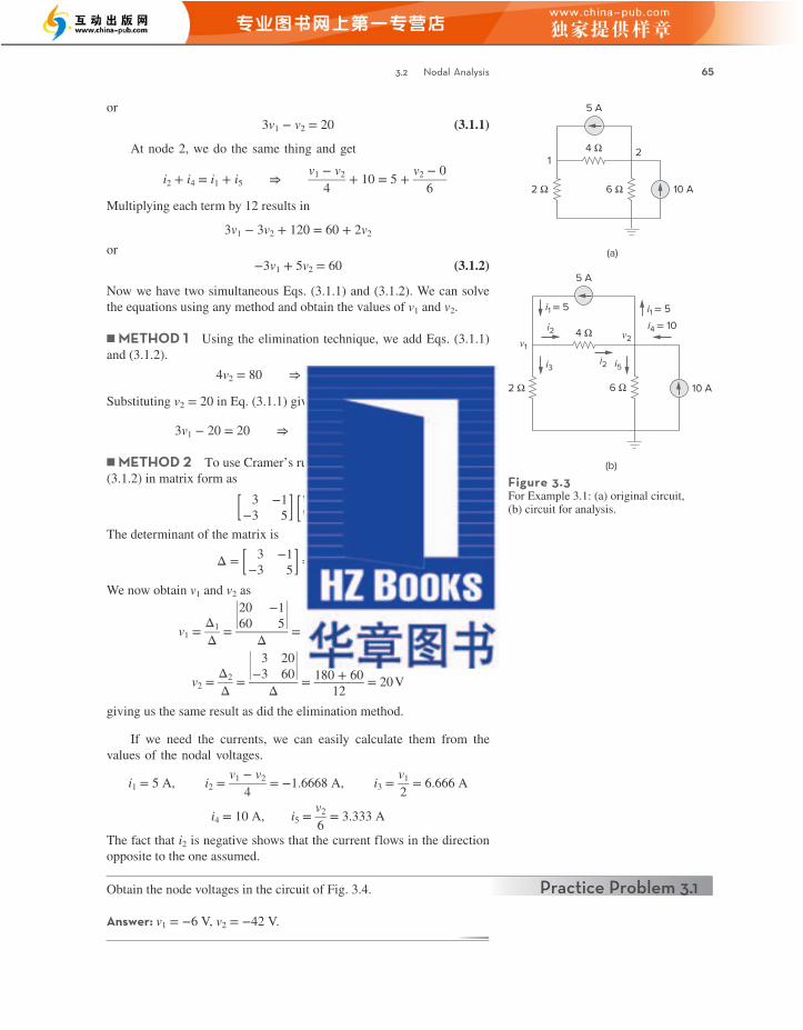
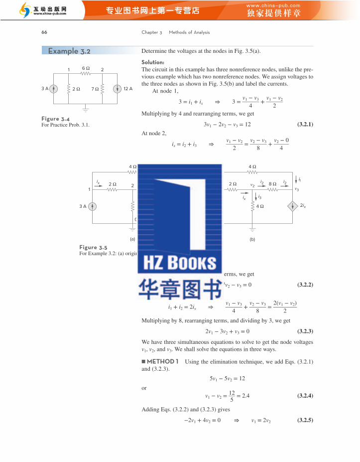
3.2 Nodal Analysis 67
Substituting Eq. (3.2.5) into Eq. (3.2.4) yields
2v2 − v2 = 2.4 ⇒ v2 = 2.4, v1 = 2v2 = 4.8 V
From Eq. (3.2.3), we get
v3 = 3v2 − 2v1 = 3v2 − 4v2 = −v2 = −2.4 V
Thus,
v1 = 4.8 V, v2 = 2.4 V, v3 = −2.4 V
METHOD 2 To use Cramer’s rule, we put Eqs. (3.2.1) to (3.2.3) in matrix form.
[
3−4
2
−27
−3
−1−1
1 ] [ v1
v2
v3 ] =
[ 1200 ]
(3.2.6)
From this, we obtain
v1 = Δ1 ___ Δ
, v2 = Δ2 ___ Δ
, v3 = Δ3 ___ Δ
where Δ, Δ1, Δ2, and Δ3 are the determinants to be calculated as follows. As explained in Appendix A, to calculate the determinant of a 3 by 3 matrix, we repeat the first two rows and cross multiply.
Δ = ǀ 3 −4 2
−2
7 −3
−1
−1 1
ǀ = ǀ 3 −4
2 3
−4
−2
7
−3 −2
7
−1
−1
1 −1
−1
ǀ = 21 − 12 + 4 + 14 − 9 − 8 = 10
Similarly, we obtain
Δ1 = ǀ 12
0
0 12
0
−2
7
−3 −2
7
−1
−1
1 −1
−1
ǀ = 84 + 0 + 0 − 0 − 36 − 0 = 48
Δ2 = ǀ 3 −4
2 3
−4
12
0
0 12
0
−1
−1
1 −1
−1
ǀ = 0 + 0 − 24 − 0 − 0 + 48 = 24
Δ3 = ǀ 3 −4
2 3
−4
−2
7
−3 −2
7
12
0
0 12
0
ǀ = 0 + 144 + 0 − 168 − 0 − 0 = −24
− − −
+ + +
− − −
+ + +
− − −
+ + +
− − −
+ + +
aLe26409_ch03_079-124.indd 85 9/27/19 1:29 PM
66 Chapter 3 Methods of Analysis
Figure 3.5For Example 3.2: (a) original circuit, (b) circuit for analysis.
4 Ω
4 Ω
2 Ω 8 Ωix1 3
2
0
3 A 2ix
(a)
ix ix i3
4 Ω
4 Ω
2 Ω 8 Ωi1
v1v2
i2 i2i1
v3
3 A
3 A
2ix
(b)
Example 3.2 Determine the voltages at the nodes in Fig. 3.5(a).
Solution:The circuit in this example has three nonreference nodes, unlike the pre-vious example which has two nonreference nodes. We assign voltages to the three nodes as shown in Fig. 3.5(b) and label the currents.
At node 1,
3 = i1 + ix ⇒ 3 = v1 − v3 ______
4 + v1 − v2 ______
2
Multiplying by 4 and rearranging terms, we get
3v1 − 2v2 − v3 = 12 (3.2.1)At node 2,
ix = i2 + i3 ⇒ v1 − v2 ______ 2 =
v2 − v3 ______ 8 + v2 − 0 ______
4
Figure 3.4For Practice Prob. 3.1.
3 A 12 A
6 Ω
2 Ω 7 Ω
1 2
Multiplying by 8 and rearranging terms, we get
−4v1 + 7v2 − v3 = 0 (3.2.2)At node 3,
i1 + i2 = 2ix ⇒ v1 − v3 ______
4 +
v2 − v3 ______ 8 = 2(v1 − v2) _________
2
Multiplying by 8, rearranging terms, and dividing by 3, we get
2v1 − 3v2 + v3 = 0 (3.2.3)
We have three simultaneous equations to solve to get the node voltages v1, v2, and v3. We shall solve the equations in three ways.
METHOD 1 Using the elimination technique, we add Eqs. (3.2.1) and (3.2.3).
5v1 − 5v2 = 12or v1 − v2 = 12 ___
5 = 2.4 (3.2.4)
Adding Eqs. (3.2.2) and (3.2.3) gives
−2v1 + 4v2 = 0 ⇒ v1 = 2v2 (3.2.5)
aLe26409_ch03_079-124.indd 84 9/27/19 1:29 PM
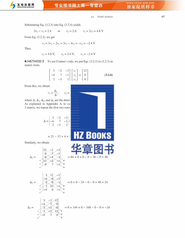
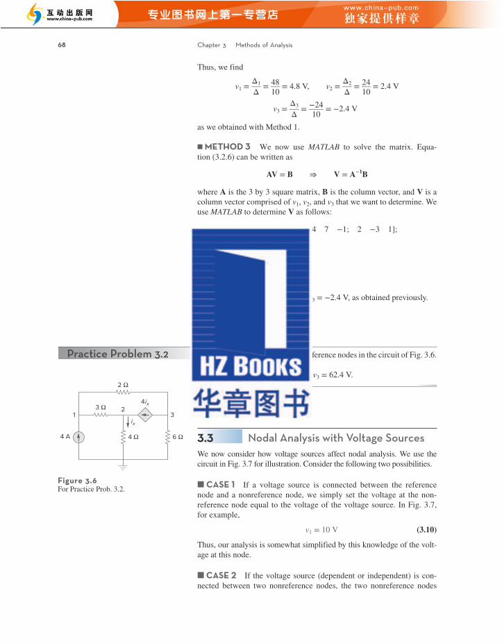
A supernode is formed by enclosing a (dependent or independent) volt-age source connected between two nonreference nodes and any ele-ments connected in parallel with it.
form a generalized node or supernode; we apply both KCL and KVL to determine the node voltages.
3.3 Nodal Analysis with Voltage Sources 69
Figure 3.7A circuit with a supernode.
10 V
5 V
4 Ω
8 Ω 6 Ω
2 Ωv1 v3
v2
i3
i1
i2
i4
Supernode
+–
+ –
A supernode may be regarded as a closed surface enclosing the voltage source and its two nodes.
In Fig. 3.7, nodes 2 and 3 form a supernode. (We could have more than two nodes forming a single supernode. For example, see the circuit in Fig. 3.14.) We analyze a circuit with supernodes using the same three steps mentioned in the previous section except that the supernodes are treated differently. Why? Because an essential component of nodal anal-ysis is applying KCL, which requires knowing the current through each element. There is no way of knowing the current through a voltage source in advance. However, KCL must be satisfied at a supernode like any other node. Hence, at the super node in Fig. 3.7,
i1 + i4 = i2 + i3 (3.11a)
or
v1 − v2 ______ 2 +
v1 − v3 ______ 4 = v2 − 0 ______
8 +
v3 − 0 ______
6 (3.11b)
To apply Kirchhoff’s voltage law to the supernode in Fig. 3.7, we redraw the circuit as shown in Fig. 3.8. Going around the loop in the clockwise direction gives
−v2 + 5 + v3 = 0 ⇒ v2 − v3 = 5 (3.12)
From Eqs. (3.10), (3.11b), and (3.12), we obtain the node voltages.Note the following properties of a supernode:
1. The voltage source inside the supernode provides a constraint equation needed to solve for the node voltages.
2. A supernode has no voltage of its own.3. A supernode requires the application of both KCL and KVL.
+ –
v2 v3
5 V
+ +
– –
Figure 3.8Applying KVL to a supernode.
aLe26409_ch03_079-124.indd 87 9/27/19 1:29 PM
68 Chapter 3 Methods of Analysis
Thus, we find
v1 = Δ1 ___ Δ
= 48 ___ 10
= 4.8 V, v2 = Δ2 ___ Δ
= 24 ___ 10
= 2.4 V
v3 = Δ3 ___ Δ
= −24 ____ 10
= −2.4 V
as we obtained with Method 1.
METHOD 3 We now use MATLAB to solve the matrix. Equa-tion (3.2.6) can be written as
AV = B ⇒ V = A−1B
where A is the 3 by 3 square matrix, B is the column vector, and V is a column vector comprised of v1, v2, and v3 that we want to determine. We use MATLAB to determine V as follows:
>>A = [3 −2 −1; −4 7 −1; 2 −3 1];>>B = [12 0 0]ʹ;>>V = inv(A) * B
V = 4.8000
2.4000 −2.4000
Thus, v1 = 4.8 V, v2 = 2.4 V, and v3 = −2.4 V, as obtained previously.
Practice Problem 3.2 Find the voltages at the three nonreference nodes in the circuit of Fig. 3.6.
Answer: v1 = 32 V, v2 = −25.6 V, v3 = 62.4 V.
Figure 3.6For Practice Prob. 3.2.
4 A
2 Ω
3 Ω
4 Ω 6 Ω
ix
4ix
1 32
3.3 Nodal Analysis with Voltage SourcesWe now consider how voltage sources affect nodal analysis. We use the circuit in Fig. 3.7 for illustration. Consider the following two possibilities.
CASE 1 If a voltage source is connected between the reference node and a nonreference node, we simply set the voltage at the non-reference node equal to the voltage of the voltage source. In Fig. 3.7, for example,
v1 = 10 V (3.10)
Thus, our analysis is somewhat simplified by this knowledge of the volt-age at this node.
CASE 2 If the voltage source (dependent or independent) is con-nected between two nonreference nodes, the two nonreference nodes
aLe26409_ch03_079-124.indd 86 9/27/19 1:29 PM
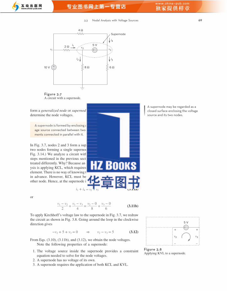

Solution:Nodes 1 and 2 form a supernode; so do nodes 3 and 4. We apply KCL to the two supernodes as in Fig. 3.13(a). At supernode 1-2,
i3 + 10 = i1 + i2
Expressing this in terms of the node voltages,
v3 − v2 ______
6 + 10 = v1 − v4 ______
3 + v1 __
2
or
5v1 + v2 − v3 − 2v4 = 60 (3.4.1)
At supernode 3-4,
i1 = i3 + i4 + i5 ⇒ v1 − v4 ______ 3 =
v3 − v2 ______ 6 + v4 __
1 +
v3 __ 4
or
4v1 + 2v2 − 5v3 − 16v4 = 0 (3.4.2)
3.3 Nodal Analysis with Voltage Sources 71
Find the node voltages in the circuit of Fig. 3.12. Example 3.4
Figure 3.12For Example 3.4.
20 V
2 Ω 4 Ω
6 Ω
3 Ω
1 Ω
vx3vx
+ – + –
10 A
1 432
+ –
3 Ω
6 Ω
2 Ω 4 Ω 1 Ω
(a)
i1
i2i3 i4i5
v1v2 v3 v4
vx+ –
(b)
+ –
+ –
20 V
3 Ω
6 Ω
i3
v1 v2 v3 v4
vx
Loop 1 Loop 2
Loop 33x
+ + ++
– – – –
i1
i3
10 A
+ –
Figure 3.13Applying: (a) KCL to the two supernodes, (b) KVL to the loops.
aLe26409_ch03_079-124.indd 89 9/27/19 1:29 PM
70 Chapter 3 Methods of Analysis
For the circuit shown in Fig. 3.9, find the node voltages.
Solution:The supernode contains the 2-V source, nodes 1 and 2, and the 10-Ω resistor. Applying KCL to the supernode as shown in Fig. 3.10(a) gives
2 = i1 + i2 + 7
Expressing i1 and i2 in terms of the node voltages
2 = v1 − 0 ______ 2 + v2 − 0 ______
4 + 7 ⇒ 8 = 2v1 + v2 + 28
or
v2 = −20 − 2v1 (3.3.1)
To get the relationship between v1 and v2, we apply KVL to the circuit in Fig. 3.10(b). Going around the loop, we obtain
−v1 − 2 + v2 = 0 ⇒ v2 = v1 + 2 (3.3.2)From Eqs. (3.3.1) and (3.3.2), we write
v2 = v1 + 2 = −20 − 2v1
or
3v1 = −22 ⇒ v1 = −7.333 V
and v2 = v1 + 2 = −5.333 V. Note that the 10-Ω resistor does not make any difference because it is connected across the supernode.
Example 3.3
Figure 3.9For Example 3.3.
+–
2 A
2 V
7 A4 Ω
10 Ω
2 Ω
v1 v2
2 A
2 A
7 A
7 A
2 Ω 4 Ω
v2v1
i1 i2
1 2
(a)
+–
(b)
2 V1 2
++
– –
v1 v2
Figure 3.10Applying: (a) KCL to the supernode, (b) KVL to the loop.
Figure 3.11For Practice Prob. 3.3.
14 V
6 V4 Ω
3 Ω 2 Ω 6 Ω+–
+–
i
v+
–
Practice Problem 3.3 Find v and i in the circuit of Fig. 3.11.
Answer: −400 mV, 2.8 A.
aLe26409_ch03_079-124.indd 88 9/27/19 1:29 PM
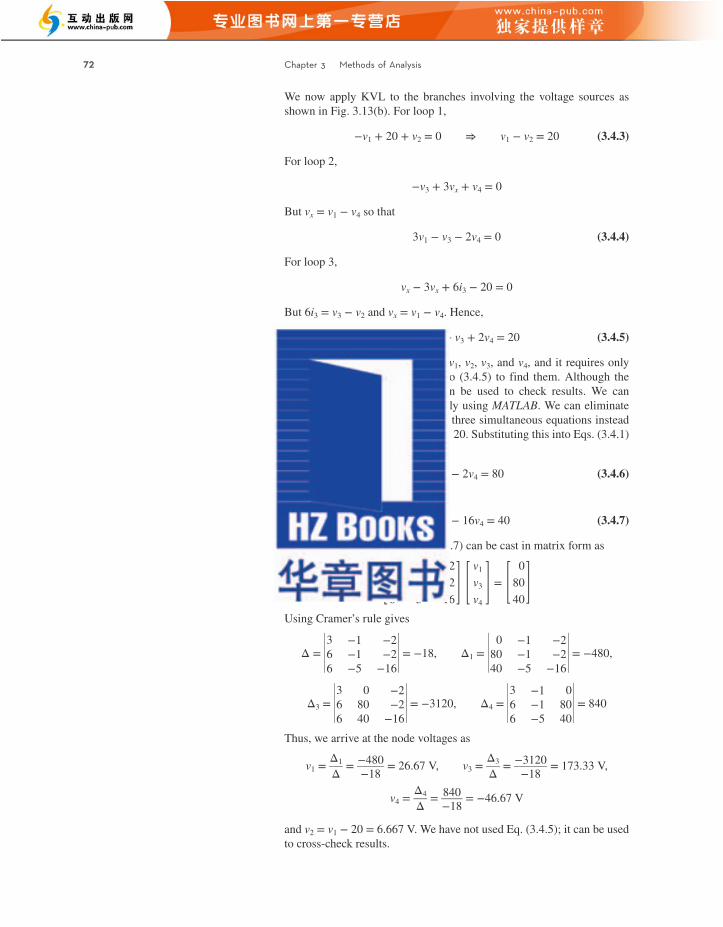
A mesh is a loop that does not contain any other loops within it.
3.4 Mesh Analysis 73
Practice Problem 3.4Find v1, v2, and v3 in the circuit of Fig. 3.14 using nodal analysis.
Answer: v1 = 7.608 V, v2 = −17.39 V, v3 = 1.6305 V.
Figure 3.14For Practice Prob. 3.4.
2 Ω 4 Ω 3 Ω
6 Ω
iv1
v2 v3
+–
5i
++ ––25 V
3.4 Mesh AnalysisMesh analysis provides another general procedure for analyzing circuits, using mesh currents as the circuit variables. Using mesh currents instead of element currents as circuit variables is convenient and reduces the number of equations that must be solved simultaneously. Recall that a loop is a closed path with no node passed more than once. A mesh is a loop that does not contain any other loop within it.
Nodal analysis applies KCL to find unknown voltages in a given circuit, while mesh analysis applies KVL to find unknown currents. Mesh analysis is not quite as general as nodal analysis because it is only applicable to a circuit that is planar. A planar circuit is one that can be drawn in a plane with no branches crossing one another; oth-erwise it is nonplanar. A circuit may have crossing branches and still be planar if it can be redrawn such that it has no crossing branches. For example, the circuit in Fig. 3.15(a) has two crossing branches, but it can be redrawn as in Fig. 3.15(b). Hence, the circuit in Fig. 3.15(a) is planar. However, the circuit in Fig. 3.16 is nonplanar, because there is no way to redraw it and avoid the branches crossing. Nonplanar circuits can be handled using nodal analysis, but they will not be considered in this text.
Mesh analysis is also known as loop analysis or the mesh-current method.
(a)
1 A
(b)
1 A
1 Ω
1 Ω 3 Ω
2 Ω
4 Ω5 Ω
8 Ω 7 Ω
6 Ω
2 Ω
4 Ω
7 Ω8 Ω
5 Ω 6 Ω 3 Ω
Figure 3.15(a) A planar circuit with crossing branches, (b) the same circuit redrawn with no cross-ing branches.
Figure 3.16A nonplanar circuit.
5 A
1 Ω
5 Ω4 Ω
6 Ω
10 Ω
11 Ω12 Ω
13 Ω
9 Ω8 Ω
3 Ω
2 Ω7 Ω
To understand mesh analysis, we should first explain more about what we mean by a mesh.
aLe26409_ch03_079-124.indd 91 9/27/19 1:29 PM
We now apply KVL to the branches involving the voltage sources as shown in Fig. 3.13(b). For loop 1,
−v1 + 20 + v2 = 0 ⇒ v1 − v2 = 20 (3.4.3)
For loop 2,
−v3 + 3vx + v4 = 0
But vx = v1 − v4 so that
3v1 − v3 − 2v4 = 0 (3.4.4)
For loop 3,
vx − 3vx + 6i3 − 20 = 0
But 6i3 = v3 − v2 and vx = v1 − v4. Hence,
−2v1 − v2 + v3 + 2v4 = 20 (3.4.5)
We need four node voltages, v1, v2, v3, and v4, and it requires only four out of the five Eqs. (3.4.1) to (3.4.5) to find them. Although the fifth equation is redundant, it can be used to check results. We can solve Eqs. (3.4.1) to (3.4.4) directly using MATLAB. We can eliminate one node voltage so that we solve three simultaneous equations instead of four. From Eq. (3.4.3), v2 = v1 − 20. Substituting this into Eqs. (3.4.1) and (3.4.2), respectively, gives
6v1 − v3 − 2v4 = 80 (3.4.6)
and
6v1 − 5v3 − 16v4 = 40 (3.4.7)
Equations (3.4.4), (3.4.6), and (3.4.7) can be cast in matrix form as
[ 366
−1−1−5
−2−2
−16 ] [ v1
v3
v4 ] =
[ 0
8040 ]
Using Cramer’s rule gives
Δ = ǀ 3 6
6
−1
−1 −5
−2
−2 −16
ǀ = −18, Δ1 = ǀ 0
80
40
−1
−1 −5
−2
−2 −16
ǀ = −480,
Δ3 = ǀ 3 6
6
0
80
40
−2
−2
−16 ǀ = −3120, Δ4 = ǀ 3
6
6
−1
−1 −5
0
80 40
ǀ = 840
Thus, we arrive at the node voltages as
v1 = Δ1 ___ Δ
= −480 _____ −18
= 26.67 V, v3 = Δ3 ___ Δ
= −3120 ______ −18
= 173.33 V,
v4 = Δ4 ___ Δ
= 840 ____ −18
= −46.67 V
and v2 = v1 − 20 = 6.667 V. We have not used Eq. (3.4.5); it can be used to cross-check results.
72 Chapter 3 Methods of Analysis
aLe26409_ch03_079-124.indd 90 9/27/19 1:29 PM
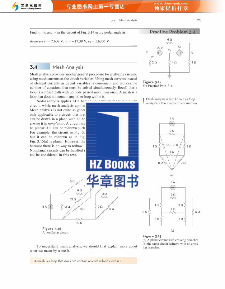
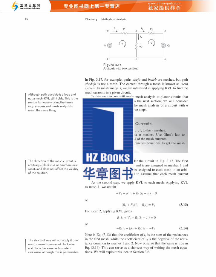
The third step is to solve for the mesh currents. Putting Eqs. (3.13) and (3.14) in matrix form yields
[ R1 + R3
−R3 −R3
R2 + R3 ] [ i1
i2 ] = [ V1
−V2 ] (3.15)
which can be solved to obtain the mesh currents i1 and i2. We are at liberty to use any technique for solving the simultaneous equations. According to Eq. (2.12), if a circuit has n nodes, b branches, and l in-dependent loops or meshes, then l = b − n + 1. Hence, l independent simultaneous equations are required to solve the circuit using mesh analysis.
Notice that the branch currents are different from the mesh currents unless the mesh is isolated. To distinguish between the two types of currents, we use i for a mesh current and I for a branch current. The current elements I1, I2, and I3 are algebraic sums of the mesh currents. It is evident from Fig. 3.17 that
I1 = i1, I2 = i2, I3 = i1 − i2 (3.16)
3.4 Mesh Analysis 75
For the circuit in Fig. 3.18, find the branch currents I1, I2, and I3 using mesh analysis.
Solution:We first obtain the mesh currents using KVL. For mesh 1,
−15 + 5i1 + 10(i1 − i2) + 10 = 0
or
3i1 − 2i2 = 1 (3.5.1)
For mesh 2,
6i2 + 4i2 + 10(i2 − i1) − 10 = 0
or i1 = 2i2 − 1 (3.5.2)
METHOD 1 Using the substitution method, we substitute Eq. (3.5.2) into Eq. (3.5.1), and write
6i2 − 3 − 2i2 = 1 ⇒ i2 = 1 A
From Eq. (3.5.2), i1 = 2i2 − 1 = 2 − 1 = 1 A. Thus,
I1 = i1 = 1 A, I2 = i2 = 1 A, I3 = i1 − i2 = 0
METHOD 2 To use Cramer’s rule, we cast Eqs. (3.5.1) and (3.5.2) in matrix form as
[ 3−1
−22 ] [ i1
i2 ] = [ 11 ]
Example 3.5
Figure 3.18For Example 3.5.
+–
+–
15 V
10 V
5 Ω 6 Ω
10 Ω
4 Ω
I1
i1
I2
i2
I3
aLe26409_ch03_079-124.indd 93 9/27/19 1:29 PM
74 Chapter 3 Methods of Analysis
Figure 3.17A circuit with two meshes.
+– +–
I1 R1 R2
R3
i1 i2
I2
I3
V1 V2
a b c
def
To illustrate the steps, consider the circuit in Fig. 3.17. The first step requires that mesh currents i1 and i2 are assigned to meshes 1 and 2. Although a mesh current may be assigned to each mesh in an arbi-trary direction, it is conventional to assume that each mesh current flows clockwise.
As the second step, we apply KVL to each mesh. Applying KVL to mesh 1, we obtain
−V1 + R1i1 + R3 (i1 − i2) = 0
or (R1 + R3) i1 − R3i2 = V1 (3.13)
For mesh 2, applying KVL gives
R2 i2 + V2 + R3 (i2 − i1) = 0
or −R3 i1 + (R2 + R3) i2 = −V2 (3.14)
Note in Eq. (3.13) that the coefficient of i1 is the sum of the resistances in the first mesh, while the coefficient of i2 is the negative of the resis-tance common to meshes 1 and 2. Now observe that the same is true in Eq. (3.14). This can serve as a shortcut way of writing the mesh equa-tions. We will exploit this idea in Section 3.6.
The direction of the mesh current is arbitrary—(clockwise or counterclock-wise)—and does not affect the validity of the solution.
Although path abcdefa is a loop and not a mesh, KVL still holds. This is the reason for loosely using the terms loop analysis and mesh analysis to mean the same thing.
In Fig. 3.17, for example, paths abefa and bcdeb are meshes, but path abcdefa is not a mesh. The current through a mesh is known as mesh current. In mesh analysis, we are interested in applying KVL to find the mesh currents in a given circuit.
In this section, we will apply mesh analysis to planar circuits that do not contain current sources. In the next section, we will consider circuits with current sources. In the mesh analysis of a circuit with n meshes, we take the following three steps.
The shortcut way will not apply if one mesh current is assumed clockwise and the other assumed counter- clockwise, although this is permissible.
Steps to Determine Mesh Currents:1. Assign mesh currents i1, i2, . . . , in to the n meshes.2. Apply KVL to each of the n meshes. Use Ohm’s law to
express the voltages in terms of the mesh currents.3. Solve the resulting n simultaneous equations to get the mesh
currents.
aLe26409_ch03_079-124.indd 92 9/27/19 1:29 PM
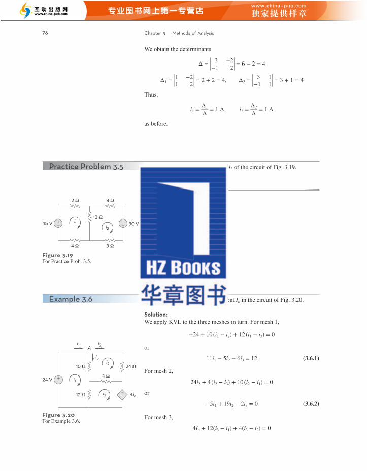
But at node A, Io = i1 − i2, so that
4(i1 − i2) + 12(i3 − i1) + 4(i3 − i2) = 0
or −i1 − i2 + 2i3 = 0 (3.6.3)
In matrix form, Eqs. (3.6.1) to (3.6.3) become
[ 11−5−1
−519−1
−6−2
2 ] [ i1
i2
i3 ] =
[ 1200 ]
We obtain the determinants as
Δ = ǀ 11
−5
−1 11
−5
−5
19
−1 −5
19
−6
−2
2 −6
−2
ǀ = 418 − 30 − 10 − 114 − 22 − 50 = 192
Δ1 = ǀ 12
0
0 12
0
−5
19
−1 −5
19
−6
−2
2 −6
−2
ǀ = 456 − 24 = 432
Δ2 = ǀ 11
−5
−1 11
−5
12
0
0 12
0
−6
−2
2 −6
−2
ǀ = 24 + 120 = 144
Δ3 = ǀ 11
−5
−1 11
−5
−5
19
−1 −5
19
12
0
0 12
0
ǀ = 60 + 228 = 288
We calculate the mesh currents using Cramer’s rule as
i1 = Δ1 ___ Δ
= 432 ____ 192
= 2.25 A, i2 = Δ2 ___ Δ
= 144 ____ 192
= 0.75 A,
i3 = Δ3 ___ Δ
= 288 ____ 192
= 1.5 A
Thus, Io = i1 − i2 = 1.5 A.
3.4 Mesh Analysis 77
− − −
+ + +
− − −
+ + +
− − −
+ + +
− − −
+ + +
aLe26409_ch03_079-124.indd 95 9/27/19 1:29 PM
We obtain the determinants
Δ = ǀ 3 −1
−2 2 ǀ = 6 − 2 = 4
Δ1 = ǀ 1 1 −2
2 ǀ = 2 + 2 = 4, Δ2 = ǀ 3
−1 1
1 ǀ = 3 + 1 = 4
Thus,
i1 = Δ1 ___ Δ
= 1 A, i2 = Δ2 ___ Δ
= 1 A
as before.
76 Chapter 3 Methods of Analysis
Calculate the mesh currents i1 and i2 of the circuit of Fig. 3.19.
Answer: i1 = 2.5 A, i2 = 0 A.
Practice Problem 3.5
45 V 30 V
2 Ω
4 Ω 3 Ω
12 Ω
9 Ω
i1i2
+– +–
Figure 3.19For Practice Prob. 3.5.
+–
+–
24 V
12 Ω
4 Ω
10 Ω 24 Ω
i1
i1
i3
i2
i2Io
4Io
A
Figure 3.20For Example 3.6.
Example 3.6 Use mesh analysis to find the current Io in the circuit of Fig. 3.20.
Solution:We apply KVL to the three meshes in turn. For mesh 1,
−24 + 10 (i1 − i2) + 12 (i1 − i3) = 0
or
11i1 − 5i2 − 6i3 = 12 (3.6.1)
For mesh 2,
24i2 + 4 (i2 − i3) + 10 (i2 − i1) = 0
or
−5i1 + 19i2 − 2i3 = 0 (3.6.2)
For mesh 3,
4Io + 12(i3 − i1) + 4(i3 − i2) = 0
aLe26409_ch03_079-124.indd 94 9/27/19 1:29 PM
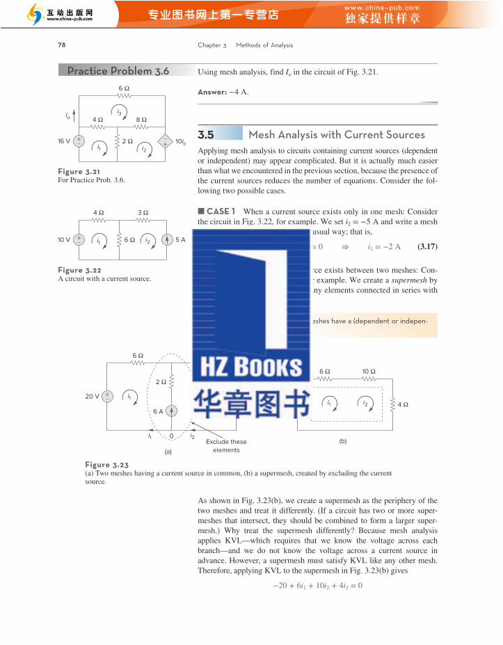
or
6i1 + 14i2 = 20 (3.18)
We apply KCL to a node in the branch where the two meshes intersect. Applying KCL to node 0 in Fig. 3.23(a) gives
i2 = i1 + 6 (3.19)
Solving Eqs. (3.18) and (3.19), we get
i1 = −3.2 A, i2 = 2.8 A (3.20)
Note the following properties of a supermesh:
1. The current source in the supermesh provides the constraint equation necessary to solve for the mesh currents.
2. A supermesh has no current of its own.3. A supermesh requires the application of both KVL and KCL.
3.5 Mesh Analysis with Current Sources 79
For the circuit in Fig. 3.24, find i1 to i4 using mesh analysis. Example 3.7
+– 10 V6 Ω 8 Ω
2 Ω4 Ω
i1
i2 i3 i4
2 Ω
5 A
i1
i2
i2 i3
Io
P
Q
3Io
Figure 3.24For Example 3.7.
Solution:Note that meshes 1 and 2 form a supermesh because they have an inde-pendent current source in common. Also, meshes 2 and 3 form another supermesh because they have a dependent current source in common. The two supermeshes intersect and form a larger supermesh as shown. Applying KVL to the larger supermesh,
2i1 + 4i3 + 8(i3 − i4) + 6i2 = 0or i1 + 3i2 + 6i3 − 4i4 = 0 (3.7.1)
For the independent current source, we apply KCL to node P:
i2 = i1 + 5 (3.7.2)
For the dependent current source, we apply KCL to node Q:
i2 = i3 + 3Io
aLe26409_ch03_079-124.indd 97 9/27/19 1:29 PM
78 Chapter 3 Methods of Analysis
Using mesh analysis, find Io in the circuit of Fig. 3.21.
Answer: −4 A.
Practice Problem 3.6
+––+16 V
4 Ω 8 Ω
2 Ω
6 Ω
i1 i2
i3
10io
Io
Figure 3.21For Practice Prob. 3.6.
+– 5 A10 V
4 Ω 3 Ω
6 Ωi1 i2
Figure 3.22A circuit with a current source.
A supermesh results when two meshes have a (dependent or indepen-dent) current source in common.
(b)
20 V 4 Ω
6 Ω 10 Ω
i1 i2+–
+–
6 A
20 V
6 Ω 10 Ω
2 Ω
4 Ω
i1
i1
i2
i2
0
(a)
Exclude theseelements
Figure 3.23(a) Two meshes having a current source in common, (b) a supermesh, created by excluding the current source.
3.5 Mesh Analysis with Current SourcesApplying mesh analysis to circuits containing current sources (dependent or independent) may appear complicated. But it is actually much easier than what we encountered in the previous section, because the presence of the current sources reduces the number of equations. Consider the fol-lowing two possible cases.
CASE 1 When a current source exists only in one mesh: Consider the circuit in Fig. 3.22, for example. We set i2 = −5 A and write a mesh equation for the other mesh in the usual way; that is,
−10 + 4i1 + 6(i1 − i2) = 0 ⇒ i1 = −2 A (3.17)
CASE 2 When a current source exists between two meshes: Con-sider the circuit in Fig. 3.23(a), for example. We create a supermesh by excluding the current source and any elements connected in series with it, as shown in Fig. 3.23(b). Thus,
As shown in Fig. 3.23(b), we create a supermesh as the periphery of the two meshes and treat it differently. (If a circuit has two or more super-meshes that intersect, they should be combined to form a larger super-mesh.) Why treat the supermesh differently? Because mesh analysis applies KVL—which requires that we know the voltage across each branch—and we do not know the voltage across a current source in advance. However, a supermesh must satisfy KVL like any other mesh. Therefore, applying KVL to the supermesh in Fig. 3.23(b) gives
−20 + 6i1 + 10i2 + 4i2 = 0
aLe26409_ch03_079-124.indd 96 9/27/19 1:29 PM
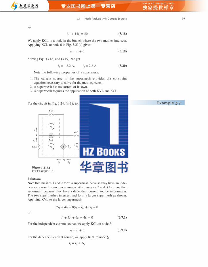
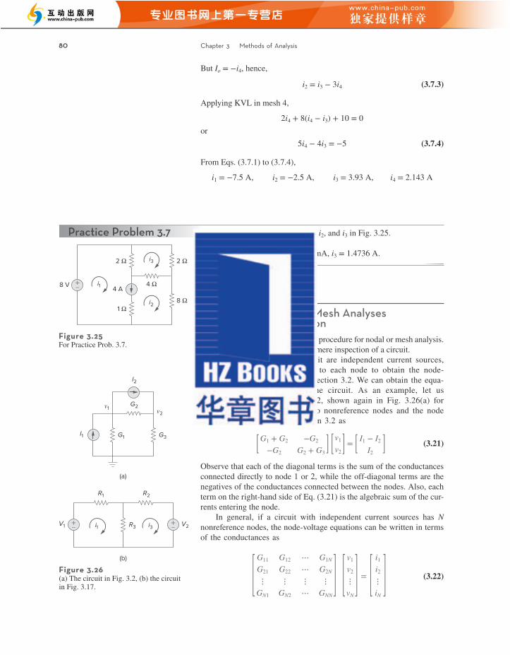
3.6 Nodal and Mesh Analyses by Inspection 81
or simply
Gv = i (3.23)
where
Gkk = Sum of the conductances connected to node k Gk j = Gjk = Negative of the sum of the conductances directly
connecting nodes k and j, k ≠ j vk = Unknown voltage at node k
ik = Sum of all independent current sources directly connected to node k, with currents entering the node treated as positive
G is called the conductance matrix; v is the output vector; and i is the input vector. Equation (3.22) can be solved to obtain the unknown node voltages. Keep in mind that this is valid for circuits with only indepen-dent current sources and linear resistors.
Similarly, we can obtain mesh-current equations by inspection when a linear resistive circuit has only independent voltage sources. Consider the circuit in Fig. 3.17, shown again in Fig. 3.26(b) for con-venience. The circuit has two nonreference nodes and the node equa-tions were derived in Section 3.4 as
[ R1 + R3
−R3 −R3
R2 + R3 ] [ i1
i2 ] = [ v1
−v2 ] (3.24)
We notice that each of the diagonal terms is the sum of the resistances in the related mesh, while each of the off-diagonal terms is the negative of the resistance common to meshes 1 and 2. Each term on the right-hand side of Eq. (3.24) is the algebraic sum taken clockwise of all independent voltage sources in the related mesh.
In general, if the circuit has N meshes, the mesh-current equations can be expressed in terms of the resistances as
[ R11
R21
⋮RN1
R12
R22
⋮RN2
⋯⋯⋮⋯
R1N
R2N
⋮RNN ] [
i1
i2
⋮iN ]
=
[ v1
v2
⋮vN ]
(3.25)
or simply
Ri = v (3.26)
where
Rkk = Sum of the resistances in mesh kRkj = Rjk = Negative of the sum of the resistances in common with
meshes k and j, k ≠ j ik = Unknown mesh current for mesh k in the clockwise direction
vk = Sum taken clockwise of all independent voltage sources in mesh k, with voltage rise treated as positive
R is called the resistance matrix; i is the output vector; and v is the input vector. We can solve Eq. (3.25) to obtain the unknown mesh currents.
aLe26409_ch03_079-124.indd 99 9/27/19 1:30 PM
But Io = −i4, hence,
i2 = i3 − 3i4 (3.7.3)
Applying KVL in mesh 4,
2i4 + 8(i4 − i3) + 10 = 0or 5i4 − 4i3 = −5 (3.7.4)
From Eqs. (3.7.1) to (3.7.4),
i1 = −7.5 A, i2 = −2.5 A, i3 = 3.93 A, i4 = 2.143 A
80 Chapter 3 Methods of Analysis
Use mesh analysis to determine i1, i2, and i3 in Fig. 3.25.
Answer: i1 = 4.632 A, i2 = 631.6 mA, i3 = 1.4736 A.
Practice Problem 3.7
+– 4 A8 V
1 Ω
2 Ω 2 Ω
8 Ω
4 Ωi1
i3
i2
Figure 3.25For Practice Prob. 3.7.
I1
v1
G1 G3
G2
I2
v2
(a)
(b)
i1 i3V1 V2+– +–
R1 R2
R3
Figure 3.26(a) The circuit in Fig. 3.2, (b) the circuit in Fig. 3.17.
3.6 Nodal and Mesh Analyses by Inspection
This section presents a generalized procedure for nodal or mesh analysis. It is a shortcut approach based on mere inspection of a circuit.
When all sources in a circuit are independent current sources, we do not need to apply KCL to each node to obtain the node-voltage equations as we did in Section 3.2. We can obtain the equa-tions by mere inspection of the circuit. As an example, let us reexamine the circuit in Fig. 3.2, shown again in Fig. 3.26(a) for convenience. The circuit has two nonreference nodes and the node equations were derived in Section 3.2 as
[ G1 + G2
−G2 −G2
G2 + G3 ] [ v1
v2 ] = [ I1 − I2
I2 ] (3.21)
Observe that each of the diagonal terms is the sum of the conductances connected directly to node 1 or 2, while the off-diagonal terms are the negatives of the conductances connected between the nodes. Also, each term on the right-hand side of Eq. (3.21) is the algebraic sum of the cur-rents entering the node.
In general, if a circuit with independent current sources has N nonreference nodes, the node-voltage equations can be written in terms of the conductances as
[ G11
G21
⋮GN1
G12
G22
⋮GN2
⋯⋯⋮⋯
G1N
G2N
⋮GNN ] [
v1
v2
⋮vN ]
=
[ i1
i2
⋮iN ]
(3.22)
aLe26409_ch03_079-124.indd 98 9/27/19 1:30 PM
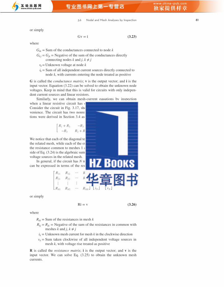
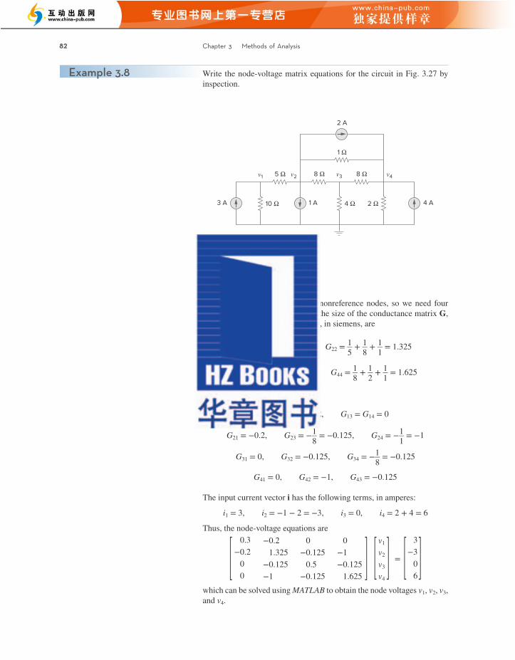
3.6 Nodal and Mesh Analyses by Inspection 83
+–
+ –
+–
+–10 V
4 V
2 Ω
2 Ω
5 Ω
2 Ω
4 Ω
3 Ω
3 Ω
1 Ω 1 Ω
4 Ω
i1
i2
i3
i4 i5 6 V12 V
Figure 3.29For Example 3.9.
Figure 3.28For Practice Prob. 3.8.
3 A
2 A
2 A
20 Ω
1 Ω
5 Ω
4 Ω
1 Ωv1 v2
v3 v4
By inspection, obtain the node-voltage equations for the circuit in Fig. 3.28.
Answer:
[
1.25 −0.2 −1 0
−0.2 0.2 0 0
−1 0 1.25 −0.25
0 0 −0.25 1.25
] [
v1
v2
v3
v4 ]
=
[
05
−32
]
Practice Problem 3.8
Example 3.9By inspection, write the mesh-current equations for the circuit in Fig. 3.29.
Solution:We have five meshes, so the resistance matrix is 5 by 5. The diagonal terms, in ohms, are:
R11 = 5 + 2 + 2 = 9, R22 = 2 + 4 + 1 + 1 + 2 = 10,R33 = 2 + 3 + 4 = 9, R44 = 1 + 3 + 4 = 8, R55 = 1 + 3 = 4
The off-diagonal terms are:
R12 = −2, R13 = −2, R14 = 0 = R15,R21 = −2, R23 = −4, R24 = −1, R25 = −1,
R31 = −2, R32 = −4, R34 = 0 = R35,R41 = 0, R42 = −1, R43 = 0, R45 = −3,R51 = 0, R52 = −1, R53 = 0, R54 = −3
The input voltage vector v has the following terms in volts:
v1 = 4, v2 = 10 − 4 = 6,v3 = −12 + 6 = −6, v4 = 0, v5 = −6
aLe26409_ch03_079-124.indd 101 9/27/19 1:30 PM
82 Chapter 3 Methods of Analysis
3 A 1 A 4 A
2 A
10 Ω
5 Ω
1 Ω
8 Ω 8 Ωv1 v2 v3 v4
4 Ω 2 Ω
Figure 3.27For Example 3.8.
Example 3.8 Write the node-voltage matrix equations for the circuit in Fig. 3.27 by inspection.
Solution:The circuit in Fig. 3.27 has four nonreference nodes, so we need four node equations. This implies that the size of the conductance matrix G, is 4 by 4. The diagonal terms of G, in siemens, are
G11 = 1 __ 5 + 1 ___
10 = 0.3, G22 = 1 __
5 + 1 __
8 + 1 __
1 = 1.325
G33 = 1 __ 8 + 1 __
8 + 1 __
4 = 0.5, G44 = 1 __
8 + 1 __
2 + 1 __
1 = 1.625
The off-diagonal terms are
G12 = − 1 __ 5 = −0.2, G13 = G14 = 0
G21 = −0.2, G23 = − 1 __ 8 = −0.125, G24 = − 1 __
1 = −1
G31 = 0, G32 = −0.125, G34 = − 1 __ 8 = −0.125
G41 = 0, G42 = −1, G43 = −0.125
The input current vector i has the following terms, in amperes:
i1 = 3, i2 = −1 − 2 = −3, i3 = 0, i4 = 2 + 4 = 6
Thus, the node-voltage equations are
[
0.3 −0.2 0 0
−0.2 1.325 −0.125 −1
0 −0.125 0.5 −0.125
0 −1 −0.125 1.625
] [
v1
v2
v3
v4 ]
=
[
3−3
06
]
which can be solved using MATLAB to obtain the node voltages v1, v2, v3, and v4.
aLe26409_ch03_079-124.indd 100 9/27/19 1:30 PM
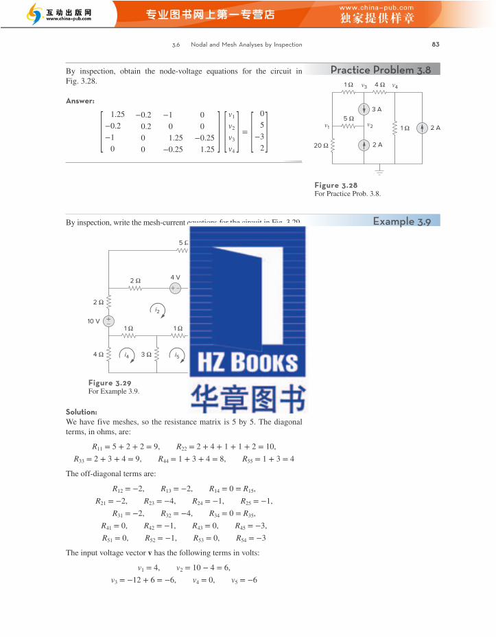
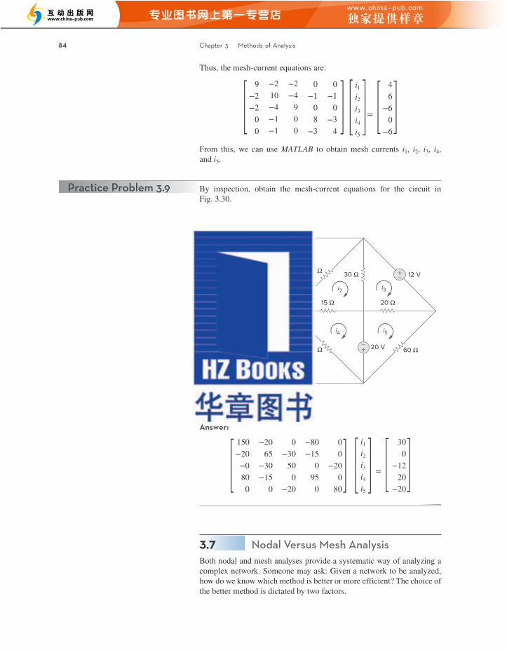
85
The first factor is the nature of the particular network. Networks that contain many series-connected elements, voltage sources, or super-meshes are more suitable for mesh analysis, whereas networks with parallel-connected elements, current sources, or supernodes are more suitable for nodal analysis. Also, a circuit with fewer nodes than meshes is better analyzed using nodal analysis, while a circuit with fewer meshes than nodes is better analyzed using mesh analysis. The key is to select the method that results in the smaller number of equations.
The second factor is the information required. If node voltages are required, it may be expedient to apply nodal analysis. If branch or mesh currents are required, it may be better to use mesh analysis.
It is helpful to be familiar with both methods of analysis, for at least two reasons. First, one method can be used to check the results from the other method, if possible. Second, since each method has its limitations, only one method may be suitable for a particular problem.
hand calculation. A computer software package based on nodal analy-sis is introduced next.
aLe26409_ch03_079-124.indd 103 9/27/19 1:30 PM
But mesh analysis cannot easily be used to solve an op amp circuit, as we shall see in Chapter 5, because there is no direct way to obtain the
Also, nodal analysis is more amenable to solution by computer, as it is easy to program. This allows one to analyze complicated circuits that defy
is the only option, because mesh analysis only applies to planar networks. voltage across the op amp itself. For nonplanar networks, nodal analysis
Problems
Sections 3.2 and 3.3 Nodal Analysis
3.1 Using Fig. 3.31, design a problem to help other students better understand nodal analysis.
3.3 Find the currents I1 through I4 and the voltage vo in the circuit of Fig. 3.33.
9 V12 V
R1 R2
R3+–
+–
Ix
Figure 3.31For Prob. 3.1 and Prob. 3.39.
3.2 For the circuit in Fig. 3.32, obtain v1 and v2.
Figure 3.32For Prob. 3.2.
Figure 3.34For Prob. 3.4.
3 A
6 A
5 Ω10 Ω
2 Ω
v1 v2
4 Ω
Figure 3.33For Prob. 3.3.
8 A 20 A 60 Ω30 Ω20 Ω10 Ω
I1 I2 I3 I4
vo
6 A 2 A
3 A
40 Ω40 Ω10 Ω20 Ω
i1 i2 i3 i4
3.4 Given the circuit in Fig. 3.34, calculate the currents i1 through i4.
Problems 84 Chapter 3 Methods of Analysis
Thus, the mesh-current equations are:
[
9 −2 −2 0 0
−2 10 −4 −1 −1
−2 −4 9 0 0
0 −1 0 8 −3
0 −1 0 −3 4
]
[
i1
i2
i3
i4
i5 ]
= [
4 6 −6 0 −6
]
From this, we can use MATLAB to obtain mesh currents i1, i2, i3, i4, and i5.
+–
+–
30 V
12 V
20 V
50 Ω
20 Ω
i1
i2 i3
i4 i5
15 Ω
30 Ω
20 Ω
60 Ω80 Ω
+–
Figure 3.30For Practice Prob. 3.9.
By inspection, obtain the mesh-current equations for the circuit in Fig. 3.30.
Practice Problem 3.9
Answer:
[
150 −20 −0 80 0
−20 65 −30 −15 0
0 −30 50 0 −20
−80 −15 0 95 0
0 0 −20 0 80
]
[
i1
i2
i3
i4
i5 ]
= [
30 0 −12 20 −20
]
3.7 Nodal Versus Mesh AnalysisBoth nodal and mesh analyses provide a systematic way of analyzing a complex network. Someone may ask: Given a network to be analyzed, how do we know which method is better or more efficient? The choice of the better method is dictated by two factors.
aLe26409_ch03_079-124.indd 102 9/27/19 1:30 PM
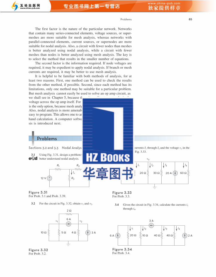

3.6 Solve for V1 in the circuit of Fig. 3.36 using nodal analysis.
Figure 3.35For Prob. 3.5.
30 V +–
2 kΩ
20 V +–
5 kΩ4 kΩ vo
+
–
Figure 3.36For Prob. 3.6.
10 Ω10 V 20 V+– +–
10 Ω
5 Ω
4 Ω
V1
+
–
10 Ω2 A 0.2Vx20 ΩVx
+
–
Figure 3.37For Prob. 3.7.
3.5 Obtain vo in the circuit of Fig. 3.35.
3.7 Apply nodal analysis to solve for Vx in the circuit of Fig. 3.37.
3.8 Using nodal analysis, find vo in the circuit of Fig. 3.38.
Figure 3.38For Prob. 3.8 and Prob. 3.37.
60 V
5vo4 Ωvo
+
– 20 Ω
6 Ω 20 Ω
+–
+–
3.9 Determine Ib in the circuit in Fig. 3.39 using nodal analysis.
Figure 3.39For Prob. 3.9.
24 V +– 50 Ω 150 Ω
60Ib250 Ω+ –
Ib
3.10 Find Io in the circuit of Fig. 3.40.
3.11 Find Vo and the power dissipated in all the resistors in the circuit of Fig. 3.41.
Figure 3.40For Prob. 3.10.
2 Ω 4 Ω8 Ω
1 Ω
4 A 2 Io
Io
Figure 3.41For Prob. 3.11.
60 V +––+12 Ω 24 V
12 Ω Vo6 Ω
3.12 Using nodal analysis, determine Vo in the circuit in Fig. 3.42.
Figure 3.42For Prob. 3.12.
20 Ω 10 Ω
20 Ω 10 Ω
40 V +– 4 Ix
Ix
Vo
+
–
aLe26409_ch03_079-124.indd 113 9/27/19 1:30 PM
86 Chapter 3 Methods of Analysis
3.13 Calculate v1 and v2 in the circuit of Fig. 3.43 using nodal analysis.
3.14 Using nodal analysis, find vo in the circuit of Fig. 3.44.
Figure 3.44For Prob. 3.14.
3.15 Apply nodal analysis to find io and the power dissipated in each resistor in the circuit of Fig. 3.45.
Figure 3.43For Prob. 3.13.
8 Ω 4 Ω 15 A
2 Ω 10 V v2v1+ –
2 Ω
12.5 A
8 Ω
+–+–4 Ω 50 Vvo
+
–
1 Ω
100 V
Figure 3.45For Prob. 3.15.
5 S6 S
2 A
io
4 A
3 S10 V
+ –
3.16 Determine voltages v1 through v3 in the circuit of Fig. 3.46 using nodal analysis.
3.17 Using nodal analysis, find current io in the circuit of Fig. 3.47.
3.18 Determine the node voltages in the circuit in Fig. 3.48 using nodal analysis.
Figure 3.46For Prob. 3.16.
1 S 13 V
2 S
v1 v2
2vo
v3
8 S
2 A 4 Svo
+
–+–
+ –
Figure 3.47For Prob. 3.17.
60 V
io
3io
10 Ω8 Ω
2 Ω
+–
4 Ω
Figure 3.48For Prob. 3.18.
15 A
231
2 Ω2 Ω
30 V
+–
8 Ω4 Ω
Figure 3.49For Prob. 3.19.
4 Ω 2 Ω
4 Ω
2 Ω
3 A
12 V
8 Ω
8 Ωv1v2
v3
5 A
+–
3.19 Use nodal analysis to find v1, v2, and v3 in the circuit of Fig. 3.49.
aLe26409_ch03_079-124.indd 114 9/27/19 1:30 PM
Problems 87
3.6 Solve for V1 in the circuit of Fig. 3.36 using nodal analysis.
Figure 3.35For Prob. 3.5.
30 V +–
2 kΩ
20 V +–
5 kΩ4 kΩ vo
+
–
Figure 3.36For Prob. 3.6.
10 Ω10 V 20 V+– +–
10 Ω
5 Ω
4 Ω
V1
+
–
10 Ω2 A 0.2Vx20 ΩVx
+
–
Figure 3.37For Prob. 3.7.
3.5 Obtain vo in the circuit of Fig. 3.35.
3.7 Apply nodal analysis to solve for Vx in the circuit of Fig. 3.37.
3.8 Using nodal analysis, find vo in the circuit of Fig. 3.38.
Figure 3.38For Prob. 3.8 and Prob. 3.37.
60 V
5vo4 Ωvo
+
– 20 Ω
6 Ω 20 Ω
+–
+–
3.9 Determine Ib in the circuit in Fig. 3.39 using nodal analysis.
Figure 3.39For Prob. 3.9.
24 V +– 50 Ω 150 Ω
60Ib250 Ω+ –
Ib
3.10 Find Io in the circuit of Fig. 3.40.
3.11 Find Vo and the power dissipated in all the resistors in the circuit of Fig. 3.41.
Figure 3.40For Prob. 3.10.
2 Ω 4 Ω8 Ω
1 Ω
4 A 2 Io
Io
Figure 3.41For Prob. 3.11.
60 V +––+12 Ω 24 V
12 Ω Vo6 Ω
3.12 Using nodal analysis, determine Vo in the circuit in Fig. 3.42.
Figure 3.42For Prob. 3.12.
20 Ω 10 Ω
20 Ω 10 Ω
40 V +– 4 Ix
Ix
Vo
+
–
aLe26409_ch03_079-124.indd 113 9/27/19 1:30 PM
86 Chapter 3 Methods of Analysis
3.13 Calculate v1 and v2 in the circuit of Fig. 3.43 using nodal analysis.
3.14 Using nodal analysis, find vo in the circuit of Fig. 3.44.
Figure 3.44For Prob. 3.14.
3.15 Apply nodal analysis to find io and the power dissipated in each resistor in the circuit of Fig. 3.45.
Figure 3.43For Prob. 3.13.
8 Ω 4 Ω 15 A
2 Ω 10 V v2v1+ –
2 Ω
12.5 A
8 Ω
+–+–4 Ω 50 Vvo
+
–
1 Ω
100 V
Figure 3.45For Prob. 3.15.
5 S6 S
2 A
io
4 A
3 S10 V
+ –
3.16 Determine voltages v1 through v3 in the circuit of Fig. 3.46 using nodal analysis.
3.17 Using nodal analysis, find current io in the circuit of Fig. 3.47.
3.18 Determine the node voltages in the circuit in Fig. 3.48 using nodal analysis.
Figure 3.46For Prob. 3.16.
1 S 13 V
2 S
v1 v2
2vo
v3
8 S
2 A 4 Svo
+
–+–
+ –
Figure 3.47For Prob. 3.17.
60 V
io
3io
10 Ω8 Ω
2 Ω
+–
4 Ω
Figure 3.48For Prob. 3.18.
15 A
231
2 Ω2 Ω
30 V
+–
8 Ω4 Ω
Figure 3.49For Prob. 3.19.
4 Ω 2 Ω
4 Ω
2 Ω
3 A
12 V
8 Ω
8 Ωv1v2
v3
5 A
+–
3.19 Use nodal analysis to find v1, v2, and v3 in the circuit of Fig. 3.49.
aLe26409_ch03_079-124.indd 114 9/27/19 1:30 PM
Problems 87

3.20 For the circuit in Fig. 3.50, find v1, v2, and v3 using nodal analysis.
3.21 For the circuit in Fig. 3.51, find v1 and v2 using nodal analysis.
Figure 3.51For Prob. 3.21.
1 kΩ
v2
vo
v1
2 kΩ
4 kΩ
3vo
3 mA
++
++
––
––
3.22 Determine v1 and v2 in the circuit of Fig. 3.52.
Figure 3.52For Prob. 3.22.
3 Av2
5vo
v1
8 Ω
1 Ω4 Ω12 V
2 Ω
vo
+––+
+ –
3.23 Use nodal analysis to find Vo in the circuit of Fig. 3.53.
Figure 3.53For Prob. 3.23.
+– 3 A30 V
1 Ω
2 Ω 16 Ω
4 Ω2Vo
+ –
Vo
+
–
3.24 Use nodal analysis and MATLAB to find Vo in the circuit of Fig. 3.54.
Figure 3.54For Prob. 3.24.
4 Ω
2 Ω1 Ω 2 Ω
2 A 4 A
8 Ω
1 Ω
Vo+ –
8 Ω 4 A 20 Ω
10 Ω 10 Ω 1 Ω
20 Ω
30 Ω v3v1
v2
v4
Figure 3.55For Prob. 3.25.
3.25 Use nodal analysis along with MATLAB to determine the node voltages in Fig. 3.55.
Figure 3.56For Prob. 3.26.
+– +
–
3 A
15 V 10 V
5 Ω 5 Ω
10 Ω
5 Ω20 Ω 15 Ω
io
4io
v2v1 v3
+–
3.26 Calculate the node voltages v1, v2, and v3 in the circuit of Fig. 3.56.
Figure 3.50For Prob. 3.20.
2 Ω
1 Ω
i
4 Ω 4 Ω
v32i
–+
12 V
v2v1
+ –
aLe26409_ch03_079-124.indd 115 9/27/19 1:30 PM
88 Chapter 3 Methods of Analysis
3.27 Use nodal analysis to determine voltages v1, v2, and v3 in the circuit of Fig. 3.57.
*
3.28 Use MATLAB to find the voltages at nodes a, b, c, and d in the circuit of Fig. 3.58.
*
Figure 3.57For Prob. 3.27.
2 S2 A 4 S 2 S 4 A
io
1 S
4 S
1 Sv1
3io
v2 v3
Figure 3.58For Prob. 3.28.
10 Ω
60 V
5 Ω
16 Ω4 Ω
4 Ω
8 Ω20 Ω
8 Ω
90 V
b
c
a
d
+–+
–
* An asterisk indicates a challenging problem.
3.30 Using nodal analysis, find vo and io in the circuit of Fig. 3.60.
Figure 3.59For Prob. 3.29.
5 A
V1 V3
V4
V21 S 4 S
2 A1 S 1 S
2 S 2 S 6 A
3 S
Figure 3.60For Prob. 3.30.
+–80 V 80 Ω vo
+
–
10 Ω 20 Ω
40 Ω 96 V
+– 2io4vo
+–
io
Figure 3.61For Prob. 3.31.
4 Ω1 A 1 Ω 4 Ω 10 V
Io
1 Ω
2 Ωv1
2vo4Io v2 v3
+–
vo
+–
+ –
3.29 Use MATLAB to solve for the node voltages in the circuit of Fig. 3.59.
Figure 3.62For Prob. 3.32.
10 kΩ4 mA
5 kΩ
v1
20 V10 V v2 v3
12 V+–
+– + –
3.32 Obtain the node voltages v1, v2, and v3 in the circuit of Fig. 3.62.
3.31 Find the node voltages for the circuit in Fig. 3.61.
aLe26409_ch03_079-124.indd 116 9/27/19 1:30 PM
Problems 89
3.20 For the circuit in Fig. 3.50, find v1, v2, and v3 using nodal analysis.
3.21 For the circuit in Fig. 3.51, find v1 and v2 using nodal analysis.
Figure 3.51For Prob. 3.21.
1 kΩ
v2
vo
v1
2 kΩ
4 kΩ
3vo
3 mA
++
++
––
––
3.22 Determine v1 and v2 in the circuit of Fig. 3.52.
Figure 3.52For Prob. 3.22.
3 Av2
5vo
v1
8 Ω
1 Ω4 Ω12 V
2 Ω
vo
+––+
+ –
3.23 Use nodal analysis to find Vo in the circuit of Fig. 3.53.
Figure 3.53For Prob. 3.23.
+– 3 A30 V
1 Ω
2 Ω 16 Ω
4 Ω2Vo
+ –
Vo
+
–
3.24 Use nodal analysis and MATLAB to find Vo in the circuit of Fig. 3.54.
Figure 3.54For Prob. 3.24.
4 Ω
2 Ω1 Ω 2 Ω
2 A 4 A
8 Ω
1 Ω
Vo+ –
8 Ω 4 A 20 Ω
10 Ω 10 Ω 1 Ω
20 Ω
30 Ω v3v1
v2
v4
Figure 3.55For Prob. 3.25.
3.25 Use nodal analysis along with MATLAB to determine the node voltages in Fig. 3.55.
Figure 3.56For Prob. 3.26.
+– +
–
3 A
15 V 10 V
5 Ω 5 Ω
10 Ω
5 Ω20 Ω 15 Ω
io
4io
v2v1 v3
+–
3.26 Calculate the node voltages v1, v2, and v3 in the circuit of Fig. 3.56.
Figure 3.50For Prob. 3.20.
2 Ω
1 Ω
i
4 Ω 4 Ω
v32i
–+
12 V
v2v1
+ –
aLe26409_ch03_079-124.indd 115 9/27/19 1:30 PM
88 Chapter 3 Methods of Analysis
3.27 Use nodal analysis to determine voltages v1, v2, and v3 in the circuit of Fig. 3.57.
*
3.28 Use MATLAB to find the voltages at nodes a, b, c, and d in the circuit of Fig. 3.58.
*
Figure 3.57For Prob. 3.27.
2 S2 A 4 S 2 S 4 A
io
1 S
4 S
1 Sv1
3io
v2 v3
Figure 3.58For Prob. 3.28.
10 Ω
60 V
5 Ω
16 Ω4 Ω
4 Ω
8 Ω20 Ω
8 Ω
90 V
b
c
a
d
+–+
–
* An asterisk indicates a challenging problem.
3.30 Using nodal analysis, find vo and io in the circuit of Fig. 3.60.
Figure 3.59For Prob. 3.29.
5 A
V1 V3
V4
V21 S 4 S
2 A1 S 1 S
2 S 2 S 6 A
3 S
Figure 3.60For Prob. 3.30.
+–80 V 80 Ω vo
+
–
10 Ω 20 Ω
40 Ω 96 V
+– 2io4vo
+–
io
Figure 3.61For Prob. 3.31.
4 Ω1 A 1 Ω 4 Ω 10 V
Io
1 Ω
2 Ωv1
2vo4Io v2 v3
+–
vo
+–
+ –
3.29 Use MATLAB to solve for the node voltages in the circuit of Fig. 3.59.
Figure 3.62For Prob. 3.32.
10 kΩ4 mA
5 kΩ
v1
20 V10 V v2 v3
12 V+–
+– + –
3.32 Obtain the node voltages v1, v2, and v3 in the circuit of Fig. 3.62.
3.31 Find the node voltages for the circuit in Fig. 3.61.
aLe26409_ch03_079-124.indd 116 9/27/19 1:30 PM
Problems 89
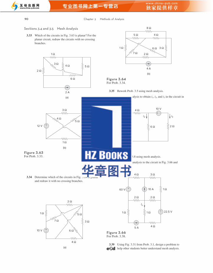
Sections 3.4 and 3.5 Mesh Analysis
3.33 Which of the circuits in Fig. 3.63 is planar? For the planar circuit, redraw the circuits with no crossing branches.
3.34 Determine which of the circuits in Fig. 3.64 is planar and redraw it with no crossing branches.
2 Ω
6 Ω
5 Ω
2 A
(a)
4 Ω3 Ω
1 Ω
Figure 3.63For Prob. 3.33.
(b)
12 V +– 2 Ω
3 Ω
5 Ω4 Ω
1 Ω
10 V +–
3 Ω
5 Ω
2 Ω
7 Ω
4 Ω
(a)
1 Ω
6 Ω
7 Ω6 Ω1 Ω 3 Ω
4 A
(b)
8 Ω
2 Ω
5 Ω 4 Ω
Figure 3.64For Prob. 3.34.
12 V
4 Ω
6 Ω 2 Ω
10 V
+–
i2i1 i3–+
Figure 3.65For Prob. 3.36.
3.35 Rework Prob. 3.5 using mesh analysis.
3.36 Use mesh analysis to obtain i1, i2, and i3 in the circuit in Fig. 3.65.
Figure 3.66For Prob. 3.38.
1 Ω
5 A
1 Ω
2 Ω 2 Ω
22.5 V
10 A60 V 1 Ω
Io
4 Ω
4 Ω 3 Ω
+–
+–
3.39 Using Fig. 3.31 from Prob. 3.1, design a problem to help other students better understand mesh analysis.
3.37 Solve Prob. 3.8 using mesh analysis.
3.38 Apply mesh analysis to the circuit in Fig. 3.66 and obtain Io.
aLe26409_ch03_079-124.indd 117 9/27/19 1:30 PM
90 Chapter 3 Methods of Analysis
3.43 Use mesh analysis to find vab and io in the circuit of Fig. 3.70.
Figure 3.67For Prob. 3.40.
56 V +–
2 kΩ
2 kΩ6 kΩ 6 kΩ
4 kΩ4 kΩ
io
Figure 3.68For Prob. 3.41.
+–
+ –
10 Ω
2 Ω
5 Ω1 Ω
8 V
6 Vi1
i2 i3
i
4 Ω
Figure 3.69For Prob. 3.42.
20 Ω 30 Ω 10 Ω
V3
V2
V140 Ω30 Ωi1
i2i3 +
–
+ –
–+
3.44 Use mesh analysis to obtain io in the circuit of Fig. 3.71.
Figure 3.70For Prob. 3.43.
+–
20 Ω
20 Ω30 Ω
30 Ω
20 Ω80 V
+–80 V
30 Ω vab
+
–
io
Figure 3.71For Prob. 3.44.
45 A
90 V
180 V
io
+ –
+–
4 Ω2 Ω
5 Ω
1 Ω
3.46 Calculate the mesh currents i1 and i2 in Fig. 3.73.
Figure 3.73For Prob. 3.46.
i1 i212 V +– 8 Ω
6 Ω3 Ω
2vo+–
+ –vo
3.41 Apply mesh analysis to find i in Fig. 3.68.
3.45 Find current i in the circuit of Fig. 3.72.
Figure 3.72For Prob. 3.45.
4 A
30 V
i+– 3 Ω 1 Ω
2 Ω 6 Ω
4 Ω 8 Ω
3.40 For the bridge network in Fig. 3.67, find io using mesh analysis.
3.42 Using Fig. 3.69, design a problem to help students better understand mesh analysis using matrices.
3.47 Rework Prob. 3.19 using mesh analysis.
aLe26409_ch03_079-124.indd 118 9/27/19 1:30 PM
Problems 91
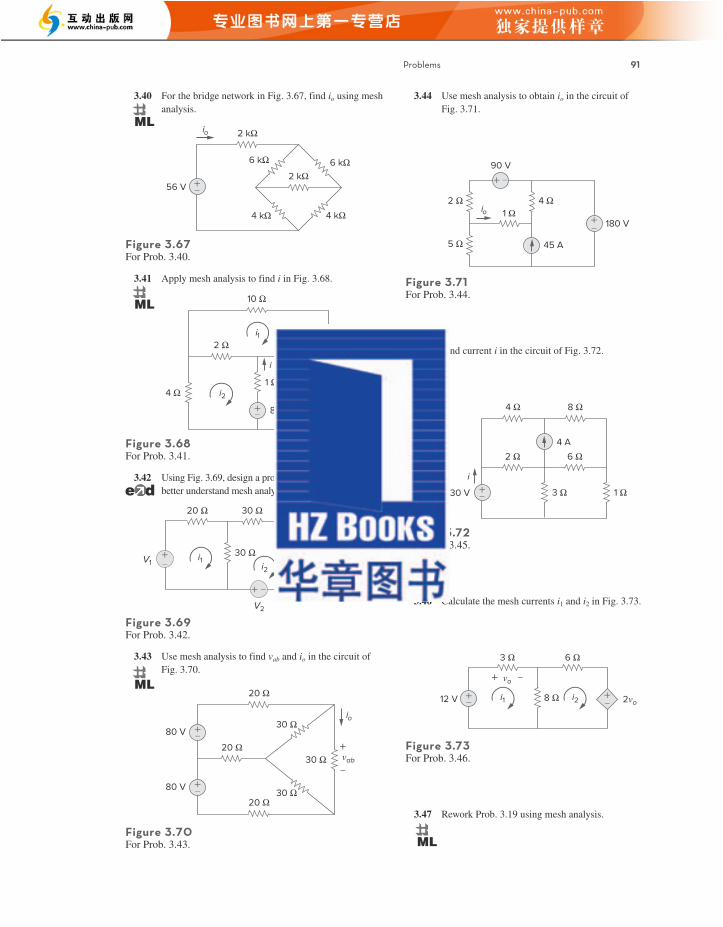
Sections 3.4 and 3.5 Mesh Analysis
3.33 Which of the circuits in Fig. 3.63 is planar? For the planar circuit, redraw the circuits with no crossing branches.
3.34 Determine which of the circuits in Fig. 3.64 is planar and redraw it with no crossing branches.
2 Ω
6 Ω
5 Ω
2 A
(a)
4 Ω3 Ω
1 Ω
Figure 3.63For Prob. 3.33.
(b)
12 V +– 2 Ω
3 Ω
5 Ω4 Ω
1 Ω
10 V +–
3 Ω
5 Ω
2 Ω
7 Ω
4 Ω
(a)
1 Ω
6 Ω
7 Ω6 Ω1 Ω 3 Ω
4 A
(b)
8 Ω
2 Ω
5 Ω 4 Ω
Figure 3.64For Prob. 3.34.
12 V
4 Ω
6 Ω 2 Ω
10 V
+–
i2i1 i3–+
Figure 3.65For Prob. 3.36.
3.35 Rework Prob. 3.5 using mesh analysis.
3.36 Use mesh analysis to obtain i1, i2, and i3 in the circuit in Fig. 3.65.
Figure 3.66For Prob. 3.38.
1 Ω
5 A
1 Ω
2 Ω 2 Ω
22.5 V
10 A60 V 1 Ω
Io
4 Ω
4 Ω 3 Ω
+–
+–
3.39 Using Fig. 3.31 from Prob. 3.1, design a problem to help other students better understand mesh analysis.
3.37 Solve Prob. 3.8 using mesh analysis.
3.38 Apply mesh analysis to the circuit in Fig. 3.66 and obtain Io.
aLe26409_ch03_079-124.indd 117 9/27/19 1:30 PM
90 Chapter 3 Methods of Analysis
3.43 Use mesh analysis to find vab and io in the circuit of Fig. 3.70.
Figure 3.67For Prob. 3.40.
56 V +–
2 kΩ
2 kΩ6 kΩ 6 kΩ
4 kΩ4 kΩ
io
Figure 3.68For Prob. 3.41.
+–
+ –
10 Ω
2 Ω
5 Ω1 Ω
8 V
6 Vi1
i2 i3
i
4 Ω
Figure 3.69For Prob. 3.42.
20 Ω 30 Ω 10 Ω
V3
V2
V140 Ω30 Ωi1
i2i3 +
–
+ –
–+
3.44 Use mesh analysis to obtain io in the circuit of Fig. 3.71.
Figure 3.70For Prob. 3.43.
+–
20 Ω
20 Ω30 Ω
30 Ω
20 Ω80 V
+–80 V
30 Ω vab
+
–
io
Figure 3.71For Prob. 3.44.
45 A
90 V
180 V
io
+ –
+–
4 Ω2 Ω
5 Ω
1 Ω
3.46 Calculate the mesh currents i1 and i2 in Fig. 3.73.
Figure 3.73For Prob. 3.46.
i1 i212 V +– 8 Ω
6 Ω3 Ω
2vo+–
+ –vo
3.41 Apply mesh analysis to find i in Fig. 3.68.
3.45 Find current i in the circuit of Fig. 3.72.
Figure 3.72For Prob. 3.45.
4 A
30 V
i+– 3 Ω 1 Ω
2 Ω 6 Ω
4 Ω 8 Ω
3.40 For the bridge network in Fig. 3.67, find io using mesh analysis.
3.42 Using Fig. 3.69, design a problem to help students better understand mesh analysis using matrices.
3.47 Rework Prob. 3.19 using mesh analysis.
aLe26409_ch03_079-124.indd 118 9/27/19 1:30 PM
Problems 91
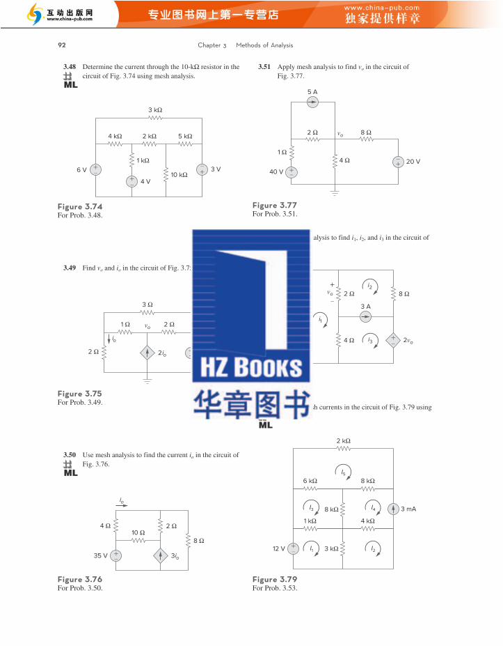
3.48 Determine the current through the 10-kΩ resistor in the circuit of Fig. 3.74 using mesh analysis.
Figure 3.74For Prob. 3.48.
6 V
4 V
3 V10 kΩ
1 kΩ
4 kΩ 2 kΩ 5 kΩ
3 kΩ
+– +
–
+–
3.49 Find vo and io in the circuit of Fig. 3.75.
Figure 3.75For Prob. 3.49.
27 V2io
3 Ω
1 Ω 2 Ω
2 Ω +–
io
vo
3.51 Apply mesh analysis to find vo in the circuit of Fig. 3.77.
Figure 3.77For Prob. 3.51.
vo
+–
–+
8 Ω2 Ω
1 Ω4 Ω 20 V
40 V
5 A
Figure 3.78For Prob. 3.52.
12 V +–
8 Ω
4 Ω +–
2 Ωvo
2vo
i2
i3
i1
3 A
+
–
Figure 3.79For Prob. 3.53.
2 kΩ
I56 kΩ 8 kΩ
8 kΩ
3 kΩ
I3 I4
1 kΩ 4 kΩ
12 V +– I2I1
3 mA
3.52 Use mesh analysis to find i1, i2, and i3 in the circuit of Fig. 3.78.
3.53 Find the mesh currents in the circuit of Fig. 3.79 using MATLAB.
3.50 Use mesh analysis to find the current io in the circuit of Fig. 3.76.
Figure 3.76For Prob. 3.50.
3io
10 Ω4 Ω
35 V +–
io
8 Ω
2 Ω
aLe26409_ch03_079-124.indd 119 9/27/19 1:30 PM
92 Chapter 3 Methods of Analysis
3.57 In the circuit of Fig. 3.83, find the values of R, V1, and V2 given that io = 15 mA.
3.56 Determine v1 and v2 in the circuit of Fig. 3.82.
Figure 3.82For Prob. 3.56.
12 V +–
v2
+
–
2 Ω
2 Ω 2 Ω
2 Ω 2 Ω
v1+ –
3.54 Find the mesh currents i1, i2, and i3 in the circuit in Fig. 3.80.
Figure 3.80For Prob. 3.54.
1 kΩ 1 kΩ 1 kΩ
12 V12 V
10 V
1 Ω1 kΩ
+–
–+
–+
i1 i2 i3
Figure 3.81For Prob. 3.55.
4 A 2 Ω
1 AI3
I1
I2
6 Ω
12 Ω 4 Ω
8 V
+ –
10 V
+ –
3.55 In the circuit of Fig. 3.81, solve for I1, I2, and I3.* Figure 3.84For Prob. 3.58.
10 Ω
10 Ω
120 V 30 Ω30 Ω
30 Ω
i3
i2
i1
+–
3.61 Calculate the current gain io∕is in the circuit of Fig. 3.86.
Figure 3.86For Prob. 3.61.
5vo
20 Ω 10 Ω
40 Ω
io
is 30 Ωvo
+
––+
3.58 Find i1, i2, and i3 in the circuit of Fig. 3.84.
Figure 3.85For Prob. 3.60.
56 V
0.5io
4 Ω 8 Ω
1 Ω 2 Ω+–
io
3.59 Rework Prob. 3.30 using mesh analysis.
3.60 Calculate the power dissipated in each resistor in the circuit of Fig. 3.85.
3.62 Find the mesh currents i1, i2, and i3 in the network of Fig. 3.87.
4 kΩ 8 kΩ 2 kΩ
100 V 4 mA 2i1 40 V+–
+–i1 i2 i3
Figure 3.87For Prob. 3.62.
Figure 3.83For Prob. 3.57.
3 kΩ
4 kΩ
V1
+
–
V2
+
–
io
R
90 V +–
aLe26409_ch03_079-124.indd 120 9/27/19 1:30 PM
Problems 93
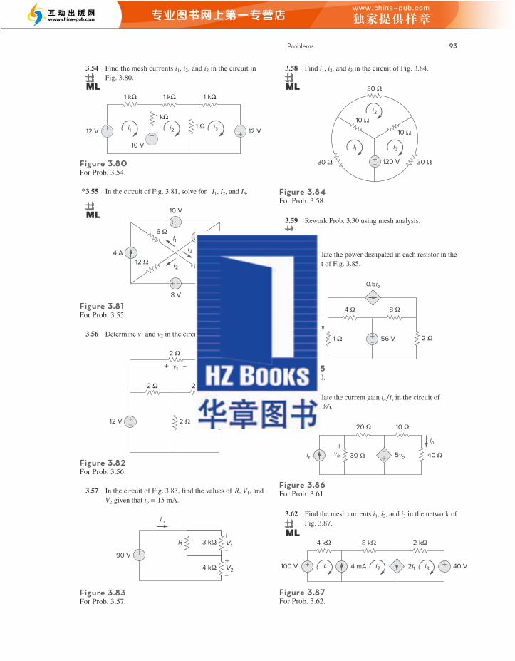
3.48 Determine the current through the 10-kΩ resistor in the circuit of Fig. 3.74 using mesh analysis.
Figure 3.74For Prob. 3.48.
6 V
4 V
3 V10 kΩ
1 kΩ
4 kΩ 2 kΩ 5 kΩ
3 kΩ
+– +
–
+–
3.49 Find vo and io in the circuit of Fig. 3.75.
Figure 3.75For Prob. 3.49.
27 V2io
3 Ω
1 Ω 2 Ω
2 Ω +–
io
vo
3.51 Apply mesh analysis to find vo in the circuit of Fig. 3.77.
Figure 3.77For Prob. 3.51.
vo
+–
–+
8 Ω2 Ω
1 Ω4 Ω 20 V
40 V
5 A
Figure 3.78For Prob. 3.52.
12 V +–
8 Ω
4 Ω +–
2 Ωvo
2vo
i2
i3
i1
3 A
+
–
Figure 3.79For Prob. 3.53.
2 kΩ
I56 kΩ 8 kΩ
8 kΩ
3 kΩ
I3 I4
1 kΩ 4 kΩ
12 V +– I2I1
3 mA
3.52 Use mesh analysis to find i1, i2, and i3 in the circuit of Fig. 3.78.
3.53 Find the mesh currents in the circuit of Fig. 3.79 using MATLAB.
3.50 Use mesh analysis to find the current io in the circuit of Fig. 3.76.
Figure 3.76For Prob. 3.50.
3io
10 Ω4 Ω
35 V +–
io
8 Ω
2 Ω
aLe26409_ch03_079-124.indd 119 9/27/19 1:30 PM
92 Chapter 3 Methods of Analysis
3.57 In the circuit of Fig. 3.83, find the values of R, V1, and V2 given that io = 15 mA.
3.56 Determine v1 and v2 in the circuit of Fig. 3.82.
Figure 3.82For Prob. 3.56.
12 V +–
v2
+
–
2 Ω
2 Ω 2 Ω
2 Ω 2 Ω
v1+ –
3.54 Find the mesh currents i1, i2, and i3 in the circuit in Fig. 3.80.
Figure 3.80For Prob. 3.54.
1 kΩ 1 kΩ 1 kΩ
12 V12 V
10 V
1 Ω1 kΩ
+–
–+
–+
i1 i2 i3
Figure 3.81For Prob. 3.55.
4 A 2 Ω
1 AI3
I1
I2
6 Ω
12 Ω 4 Ω
8 V
+ –
10 V
+ –
3.55 In the circuit of Fig. 3.81, solve for I1, I2, and I3.* Figure 3.84For Prob. 3.58.
10 Ω
10 Ω
120 V 30 Ω30 Ω
30 Ω
i3
i2
i1
+–
3.61 Calculate the current gain io∕is in the circuit of Fig. 3.86.
Figure 3.86For Prob. 3.61.
5vo
20 Ω 10 Ω
40 Ω
io
is 30 Ωvo
+
––+
3.58 Find i1, i2, and i3 in the circuit of Fig. 3.84.
Figure 3.85For Prob. 3.60.
56 V
0.5io
4 Ω 8 Ω
1 Ω 2 Ω+–
io
3.59 Rework Prob. 3.30 using mesh analysis.
3.60 Calculate the power dissipated in each resistor in the circuit of Fig. 3.85.
3.62 Find the mesh currents i1, i2, and i3 in the network of Fig. 3.87.
4 kΩ 8 kΩ 2 kΩ
100 V 4 mA 2i1 40 V+–
+–i1 i2 i3
Figure 3.87For Prob. 3.62.
Figure 3.83For Prob. 3.57.
3 kΩ
4 kΩ
V1
+
–
V2
+
–
io
R
90 V +–
aLe26409_ch03_079-124.indd 120 9/27/19 1:30 PM
Problems 93
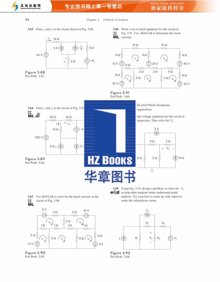
3.63 Find vx and ix in the circuit shown in Fig. 3.88.
Figure 3.88For Prob. 3.63.
ix
4ix
3 A
50 V
5 Ω
10 Ω
vx
+
–2 Ω
+–+–
vx4
3.65 Use MATLAB to solve for the mesh currents in the circuit of Fig. 3.90.
Figure 3.90For Prob. 3.65.
6 Ω
1 Ω1 Ω1 Ω
3 Ω 4 Ω
1 Ω
5 Ω6 Ω 8 Ω
2 Ω
10 V
12 V
6 V
9 V
i4
i2i1 i3
i5
+–+–
+– +
–
3.66 Write a set of mesh equations for the circuit in Fig. 3.91. Use MATLAB to determine the mesh currents.
8 Ω
10 Ω
6 Ω
2 Ω 2 Ω 6 Ω8 Ω
4 Ω 4 Ω
30 V 32 V+–
+–
12 V +– 24 V+
–+–
10 Ω
4 Ω8 Ω
40 V
8 Ωi1 i2
i5i4i3
Figure 3.91For Prob. 3.66.
Section 3.6 Nodal and Mesh Analyses by Inspection
3.67 Obtain the node-voltage equations for the circuit in Fig. 3.92 by inspection. Then solve for Vo.
3.68 Using Fig. 3.93, design a problem, to solve for Vo, to help other students better understand nodal analysis. Try your best to come up with values to make the calculations easier.
Figure 3.92For Prob. 3.67.
5 A
4 Ω 2 Ω
10 Ω 5 Ω3Vo 10 A
Vo+ –
Figure 3.93For Prob. 3.68.
R1
I2
R2 R3
R4I1 V1+–Vo
+
–
3.64 Find vo and io in the circuit of Fig. 3.89.
Figure 3.89For Prob. 3.64.
+–
+–
io + –
5 A
250 V 40 Ω
10 Ω
50 Ω 10 Ω
vo
0.2vo
4io
aLe26409_ch03_079-124.indd 121 9/27/19 1:30 PM
94 Chapter 3 Methods of Analysis
3.72 By inspection, write the mesh-current equations for the circuit in Fig. 3.97.
3.73 Write the mesh-current equations for the circuit in Fig. 3.98.
3.74 By inspection, obtain the mesh-current equations for the circuit in Fig. 3.99.
3.69 For the circuit shown in Fig. 3.94 write the node-voltage equations by inspection.
3.70 Write the node-voltage equations by inspection and then determine values of V1 and V2 in the circuit of Fig. 3.95.
Figure 3.94For Prob. 3.69.
2 kΩ 2 kΩ 10 mA20 mA
v1 4 kΩ 4 kΩ
1 kΩ
5 mA
v2 v3
Figure 3.95For Prob. 3.70.
1 S20 A 7 A
V2V1
4ix
2 S 5 S
ix
Figure 3.96For Prob. 3.71.
+–
+–
30 V
15 V
4 Ω
5 Ω
2 Ω
3 Ω
i1
i3
i2
1 Ω
3.71 Write the mesh-current equations for the circuit in Fig. 3.96. Next, determine the values of i1, i2, and i3.
+–
+–+–
10 V
4 Ω
5 Ω 2 Ω 4 Ωi1 i3 i4
8 V 4 Vi2
1 Ω
Figure 3.97For Prob. 3.72.
Figure 3.98For Prob. 3.73.
+–
+ –
6 V 4 V
1 Ω
3 Ω
1 Ω
i1 i2
i4i3
2 V
+–3 V
2 Ω
4 Ω
5 Ω
1 Ω
+–
Figure 3.99For Prob. 3.74.
+–
+ –
+–
i1
i3
V1
V3
V2V4
i2
i4
R1 R2 R3
R4
R5
R6
R7
R8
+–
aLe26409_ch03_079-124.indd 122 9/27/19 1:30 PM
Problems 95
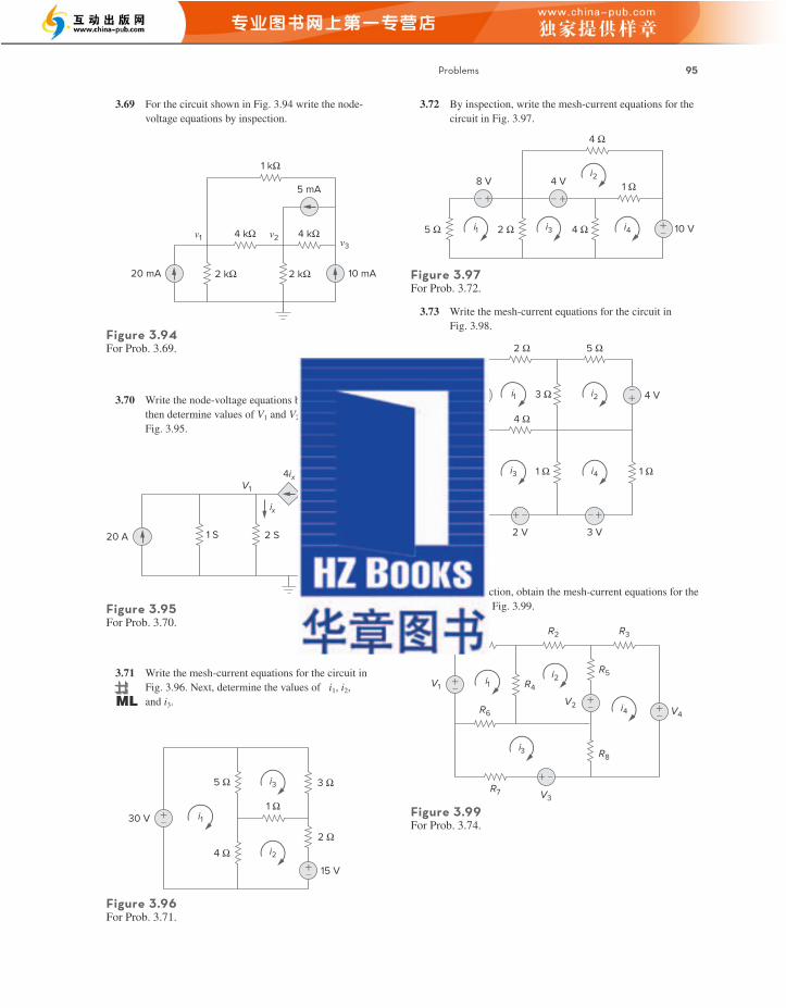
3.63 Find vx and ix in the circuit shown in Fig. 3.88.
Figure 3.88For Prob. 3.63.
ix
4ix
3 A
50 V
5 Ω
10 Ω
vx
+
–2 Ω
+–+–
vx4
3.65 Use MATLAB to solve for the mesh currents in the circuit of Fig. 3.90.
Figure 3.90For Prob. 3.65.
6 Ω
1 Ω1 Ω1 Ω
3 Ω 4 Ω
1 Ω
5 Ω6 Ω 8 Ω
2 Ω
10 V
12 V
6 V
9 V
i4
i2i1 i3
i5
+–+–
+– +
–
3.66 Write a set of mesh equations for the circuit in Fig. 3.91. Use MATLAB to determine the mesh currents.
8 Ω
10 Ω
6 Ω
2 Ω 2 Ω 6 Ω8 Ω
4 Ω 4 Ω
30 V 32 V+–
+–
12 V +– 24 V+
–+–
10 Ω
4 Ω8 Ω
40 V
8 Ωi1 i2
i5i4i3
Figure 3.91For Prob. 3.66.
Section 3.6 Nodal and Mesh Analyses by Inspection
3.67 Obtain the node-voltage equations for the circuit in Fig. 3.92 by inspection. Then solve for Vo.
3.68 Using Fig. 3.93, design a problem, to solve for Vo, to help other students better understand nodal analysis. Try your best to come up with values to make the calculations easier.
Figure 3.92For Prob. 3.67.
5 A
4 Ω 2 Ω
10 Ω 5 Ω3Vo 10 A
Vo+ –
Figure 3.93For Prob. 3.68.
R1
I2
R2 R3
R4I1 V1+–Vo
+
–
3.64 Find vo and io in the circuit of Fig. 3.89.
Figure 3.89For Prob. 3.64.
+–
+–
io + –
5 A
250 V 40 Ω
10 Ω
50 Ω 10 Ω
vo
0.2vo
4io
aLe26409_ch03_079-124.indd 121 9/27/19 1:30 PM
94 Chapter 3 Methods of Analysis
3.72 By inspection, write the mesh-current equations for the circuit in Fig. 3.97.
3.73 Write the mesh-current equations for the circuit in Fig. 3.98.
3.74 By inspection, obtain the mesh-current equations for the circuit in Fig. 3.99.
3.69 For the circuit shown in Fig. 3.94 write the node-voltage equations by inspection.
3.70 Write the node-voltage equations by inspection and then determine values of V1 and V2 in the circuit of Fig. 3.95.
Figure 3.94For Prob. 3.69.
2 kΩ 2 kΩ 10 mA20 mA
v1 4 kΩ 4 kΩ
1 kΩ
5 mA
v2 v3
Figure 3.95For Prob. 3.70.
1 S20 A 7 A
V2V1
4ix
2 S 5 S
ix
Figure 3.96For Prob. 3.71.
+–
+–
30 V
15 V
4 Ω
5 Ω
2 Ω
3 Ω
i1
i3
i2
1 Ω
3.71 Write the mesh-current equations for the circuit in Fig. 3.96. Next, determine the values of i1, i2, and i3.
+–
+–+–
10 V
4 Ω
5 Ω 2 Ω 4 Ωi1 i3 i4
8 V 4 Vi2
1 Ω
Figure 3.97For Prob. 3.72.
Figure 3.98For Prob. 3.73.
+–
+ –
6 V 4 V
1 Ω
3 Ω
1 Ω
i1 i2
i4i3
2 V
+–3 V
2 Ω
4 Ω
5 Ω
1 Ω
+–
Figure 3.99For Prob. 3.74.
+–
+ –
+–
i1
i3
V1
V3
V2V4
i2
i4
R1 R2 R3
R4
R5
R6
R7
R8
+–
aLe26409_ch03_079-124.indd 122 9/27/19 1:30 PM
Problems 95


