Embed Size (px)
Citation preview
ErikBruun
CMOSIntegratedCircuitSimulationwithLTspiceIVaTutorialGuide
Downloadfreebooksat
2
Erik Bruun
CMOS Integrated Circuit Simulation with LTspice IV – a Tutorial Guide
Download free eBooks at bookboon.com

3
CMOS Integrated Circuit Simulation with LTspice IV – a Tutorial Guide1st edition© 2015 Erik Bruun & bookboon.comISBN 978-87-403-1059-7Peer reviewed by Dennis Øland Larsen, IC design engineer, GN ReSound
Download free eBooks at bookboon.com
CMOS Integrated Circuit Simulation with LTspice IV – a Tutorial Guide
4
Contents
CMOS Integrated Circuit Simulation with LTspice IV Contents
Contents
Preface 7
Getting started 9
Tutorial 1 – Resistive Circuits 13Example 1.1: A resistor circuit. . . . . . . . . . . . . . . . . . . . . . . . . . . . . . . . 13Example 1.2: A transconductance amplifier. . . . . . . . . . . . . . . . . . . . . . . . . 27Example 1.3: A current amplifier. . . . . . . . . . . . . . . . . . . . . . . . . . . . . . 32Problems . . . . . . . . . . . . . . . . . . . . . . . . . . . . . . . . . . . . . . . . . . 38
Tutorial 2 – Circuits with Capacitors and Inductors 43Example 2.1: An RC network. . . . . . . . . . . . . . . . . . . . . . . . . . . . . . . . 43Example 2.2: A half-wave rectifier with a smoothing filter. . . . . . . . . . . . . . . . . 50Example 2.3: An amplifier with capacitive feedback network. . . . . . . . . . . . . . . . 52Example 2.4: An ideal inductor. . . . . . . . . . . . . . . . . . . . . . . . . . . . . . . 55Example 2.5: Revisiting the capacitor charging and discharging. . . . . . . . . . . . . . 57Problems . . . . . . . . . . . . . . . . . . . . . . . . . . . . . . . . . . . . . . . . . . 63
Tutorial 3 – MOS transistors 67Example 3.1: Different MOS transistor symbols and models in LTspice. . . . . . . . . . 67Example 3.2: Advanced transistor models. . . . . . . . . . . . . . . . . . . . . . . . . . 75Example 3.3: MOS transistor input characteristics. . . . . . . . . . . . . . . . . . . . . 79Example 3.4: MOS transistor output characteristics. . . . . . . . . . . . . . . . . . . . . 84Example 3.5: Deriving transistor parameters from input and output characteristics. . . . 86Example 3.6: Simulating small signal parameters using the ‘.tf’ simulation. . . . . . . . 90Problems . . . . . . . . . . . . . . . . . . . . . . . . . . . . . . . . . . . . . . . . . . 98
4
Download free eBooks at bookboon.com
CMOS Integrated Circuit Simulation with LTspice IV – a Tutorial Guide
5
ContentsCMOS Integrated Circuit Simulation with LTspice IV Contents
Tutorial 4 – Basic gain stages 103Example 4.1: The common source amplifier (inverting amplifier). . . . . . . . . . . . . 103Example 4.2: The common drain amplifier (source follower). . . . . . . . . . . . . . . . 114Example 4.3: The common gate amplifier. . . . . . . . . . . . . . . . . . . . . . . . . . 121Example 4.4: The differential pair. . . . . . . . . . . . . . . . . . . . . . . . . . . . . . 126Problems . . . . . . . . . . . . . . . . . . . . . . . . . . . . . . . . . . . . . . . . . . 140
Tutorial 5 – Hierarchical design 147Example 5.1: A two stage operational amplifier. . . . . . . . . . . . . . . . . . . . . . . 147Example 5.2: Designing the two stage opamp for an inverting feedback amplifier. . . . . 154Example 5.3: Generic filter blocks. . . . . . . . . . . . . . . . . . . . . . . . . . . . . . 165Example 5.4: A mixed analog/digital circuit. . . . . . . . . . . . . . . . . . . . . . . . . 168Problems . . . . . . . . . . . . . . . . . . . . . . . . . . . . . . . . . . . . . . . . . . 175
Tutorial 6 – Process and parameter variations 179Example 6.1: Model files for corner simulations. . . . . . . . . . . . . . . . . . . . . . 180Example 6.2: An inverter. . . . . . . . . . . . . . . . . . . . . . . . . . . . . . . . . . . 187Example 6.3: A test bench for the two stage opamp. . . . . . . . . . . . . . . . . . . . . 196Example 6.4: Monte Carlo simulation. . . . . . . . . . . . . . . . . . . . . . . . . . . . 198Problems . . . . . . . . . . . . . . . . . . . . . . . . . . . . . . . . . . . . . . . . . . 206
5
Download free eBooks at bookboon.com
Click on the ad to read more
www.sylvania.com
We do not reinvent the wheel we reinvent light.Fascinating lighting offers an infinite spectrum of possibilities: Innovative technologies and new markets provide both opportunities and challenges. An environment in which your expertise is in high demand. Enjoy the supportive working atmosphere within our global group and benefit from international career paths. Implement sustainable ideas in close cooperation with other specialists and contribute to influencing our future. Come and join us in reinventing light every day.
Light is OSRAM
CMOS Integrated Circuit Simulation with LTspice IV – a Tutorial Guide
6
ContentsCMOS Integrated Circuit Simulation with LTspice IV Contents
Tutorial 7 – Importing and exporting files 211Example 7.1: Importing a netlist file describing a current conveyor. . . . . . . . . . . . . 211Example 7.2: Creating a subcircuit from a netlist. . . . . . . . . . . . . . . . . . . . . . 215Example 7.3: Exporting a netlist. . . . . . . . . . . . . . . . . . . . . . . . . . . . . . . 221Example 7.4: Exporting other files. . . . . . . . . . . . . . . . . . . . . . . . . . . . . . 223Problems . . . . . . . . . . . . . . . . . . . . . . . . . . . . . . . . . . . . . . . . . . 227
Moving on 231
Appendix A –A beginner’s guide to components and simulation commands in LTspice 233
Appendix B –BSIM transistor models for use in LTspice 241
Index 245
6
Download free eBooks at bookboon.com
Click on the ad to read moreClick on the ad to read more
© Deloitte & Touche LLP and affiliated entities.
360°thinking.
Discover the truth at www.deloitte.ca/careers
© Deloitte & Touche LLP and affiliated entities.
360°thinking.
Discover the truth at www.deloitte.ca/careers
© Deloitte & Touche LLP and affiliated entities.
360°thinking.
Discover the truth at www.deloitte.ca/careers © Deloitte & Touche LLP and affiliated entities.
360°thinking.
Discover the truth at www.deloitte.ca/careers
CMOS Integrated Circuit Simulation with LTspice IV – a Tutorial Guide
7
Preface
CMOS Integrated Circuit Simulation with LTspice IV Preface
Preface
This book is about circuit simulation with the simulation program LTspice. It is intended as anintroduction to LTspice and to simulation of CMOS integrated circuits with LTspice. It may serveas a supplementary textbook for an introductory course in analog integrated circuit design. The firsttutorials can also be used as a general introduction to circuit simulation in an introductory coursein electronic circuits. The book can be used for classroom teaching, and it can also be used forself-study. It is based on LTspice for Windows.
Tutorials 1 and 2 introduce the fundamental concept of the circuit simulator demonstrated on circuitsusing passive devices (resistors, capacitors and inductors) and ideal voltage sources and currentsources, both independent sources and controlled sources.
7
Download free eBooks at bookboon.com
CMOS Integrated Circuit Simulation with LTspice IV – a Tutorial Guide
8
PrefaceCMOS Integrated Circuit Simulation with LTspice IV Preface
Tutorial 3 is about MOS transistor models and gives an introduction to the standard Shichman-Hodges transistor model often used for hand calculations when analyzing CMOS circuits. Also,it provides an introduction to more advanced transistor models and a comparison between the ad-vanced transistor models and the simple Shichman-Hodges model.
Tutorial 4 gives examples of basic CMOS amplifier stages, i.e. common source, common drain,common gate and differential pair. Both analysis and design approaches using LTspice are shown.
Tutorial 5 shows how the basic stages can be defined as subcircuits and combined into a multistageoperational amplifier. Also given in this tutorial is a design example of a two stage opamp fora feedback amplifier, generic filter blocks and a mixed analog/digital circuit. The tutorial is anintroduction to hierarchical design.
Tutorial 6 is about the simulation of process and parameter variations in a circuit. In integratedcircuit design, process variations pose a major challenge to the designer. Often technology filesare supplied for typical process parameters and a selection of worst case process parameters. Thetutorial gives an introduction to simulation with technology files including process variations. Alsosupply voltage variations and temperature variations are considered. Together, these variations aretermed PVT variations.
Tutorial 7 is about import of netlist files and export of output files from LTspice. The netlist filesare the primary descriptive files for a circuit to be simulated by Spice. There are minor differencesbetween netlist files originating from LTspice and other versions of Spice, but in general it is ratherstraightforward to modify a netlist file to be compatible with LTspice. Several textbooks provideexamples of netlist files which may be used for simulation with LTspice. A schematic is not needed.The simulation commands in LTspice can be executed directly from the netlist files.
End-of-chapter problems are provided for all tutorials to further illustrate the subject of the tutorials.
Finally, two appendices are included. Appendix A is a beginner’s guide which may facilitate quickand easy learning of LTspice for the reader or student who is new to LTspice. Appendix B providesa number of BSIM transistor model files for use in LTspice. The files may be copied directly fromthe electronic version of this book into a text editor.
Acknowledgements: The author would like to acknowledge the many students who have con-tributed with comments and suggestion for the book. Also, a particular acknowledgement goes tomy colleague Dennis Øland Larsen who reviewed the entire manuscript and provided many usefulcomments and corrections during the final phase of writing.
8
Download free eBooks at bookboon.com
CMOS Integrated Circuit Simulation with LTspice IV – a Tutorial Guide
9
Getting started
CMOS Integrated Circuit Simulation with LTspice IV Getting started
Getting started
The program LTspice is freely available from Linear Technology,http://www.linear.com/designtools/software/.Just click ‘Download LTspice’ and follow the instructions. You may register for an account withLinear Technology, but you do not have to. You may just click ‘No thanks, just download thesoftware’ and choose ‘Run’ in the dialogue box which appears.
A ‘Getting started guide’ is available fromhttp://cds.linear.com/docs/en/software-and-simulation/LTspiceGettingStartedGuide.pdf.This book is addressing the simulation of integrated circuits, in particular CMOS circuits, so wewill not go into detail with the simulation of circuits with standard components but refer the reader
9
CMOS Integrated Circuit Simulation with LTspice IV Getting started
to the many examples of demo circuits using standard components which are found on the LTspicewebsite. Here you will also find a blog with several hints and video clips on how to use LTspice.
In addition, comprehensive books and guides about Spice can be found, (Tuinenga 1995) and(Vladimirescu 1994), and a manual dedicated to LTspice is also available (Brocard 2013). However,the program is fairly easy and intuitive and once the installation is complete, you may go directlyto the first tutorial, providing you with examples of circuits using resistors, voltage sources and cur-rent sources. A ‘learning by doing’ approach is perfectly feasible with LTspice. The program alsoincludes a ‘help’ function with detailed descriptions of the commands and options in the program.The keyboard shortcut to ‘help’ is ‘F1’ in the windows version and ‘ ?’ in the Mac version. If youwant a paper manual for the program, you can get it using the ‘help’ function: Just open ‘help’, clickon the ‘Print’ symbol and select ‘Print the selected heading and all subtopics’ in the dialogue boxwhich opens. Your printer should be ready for printing about 130 pages.
This book is based on the Windows version of LTspice. The program is also available for Mac. Thereare some differences in the user interface of the two versions. This might be somewhat confusingfor first-time users. As a guide to Mac users, the following page provides a list of some of thedifferences which may initially cause confusion.
10
Download free eBooks at bookboon.com

CMOS Integrated Circuit Simulation with LTspice IV – a Tutorial Guide
10
Getting started
CMOS Integrated Circuit Simulation with LTspice IV Getting started
to the many examples of demo circuits using standard components which are found on the LTspicewebsite. Here you will also find a blog with several hints and video clips on how to use LTspice.
In addition, comprehensive books and guides about Spice can be found, (Tuinenga 1995) and(Vladimirescu 1994), and a manual dedicated to LTspice is also available (Brocard 2013). However,the program is fairly easy and intuitive and once the installation is complete, you may go directlyto the first tutorial, providing you with examples of circuits using resistors, voltage sources and cur-rent sources. A ‘learning by doing’ approach is perfectly feasible with LTspice. The program alsoincludes a ‘help’ function with detailed descriptions of the commands and options in the program.The keyboard shortcut to ‘help’ is ‘F1’ in the windows version and ‘ ?’ in the Mac version. If youwant a paper manual for the program, you can get it using the ‘help’ function: Just open ‘help’, clickon the ‘Print’ symbol and select ‘Print the selected heading and all subtopics’ in the dialogue boxwhich opens. Your printer should be ready for printing about 130 pages.
This book is based on the Windows version of LTspice. The program is also available for Mac. Thereare some differences in the user interface of the two versions. This might be somewhat confusingfor first-time users. As a guide to Mac users, the following page provides a list of some of thedifferences which may initially cause confusion.
10
Download free eBooks at bookboon.com
CMOS Integrated Circuit Simulation with LTspice IV – a Tutorial Guide
11
Getting startedCMOS Integrated Circuit Simulation with LTspice IV Getting started
– The toolbar shown in fig. 1.2 on page 14 is not available in the Mac version. Instead, aright click on the drawing sheet will open a menu with several sub-menus. The ‘Draft’ sub-menu allows you to insert ‘Components’, ‘Wires’, ‘Net Names’, ‘SPICE Directives’, etc.In particular, you should notice that the ground symbol is not available via ‘Components’,but it can be inserted using the keyboard shortcut (hotkey) ‘G’ or using ‘Net Names’ asexplained on page 15.
– The editing commands (‘Move’, ‘Drag’, ‘Duplicate’, etc.) are found in the ‘Edit’ sub-menu. The rotate and mirror operations are available via ‘ R’ and ‘ E’.
– The ‘Simulate’ command shown in fig. 1.2 on page 14 and described on page 16 is notavailable in the Mac version. Instead, use ‘SPICE Directives’ from the ‘Draft’ sub-menuand type in the appropriate simulation command. The help function provided by the win-dow shown in fig. 1.5 on page 18 with different tabs for the different simulation commandscan be opened by right clicking in the ‘SPICE Directives’ dialogue box. This opens a ‘Helpme edit’ option where you can select ‘Analysis Cmd’. A similar help function is availablefor ‘.step’ commands.
– The result of a ‘DC operating point’ simulation (‘.op’) is not automatically displayed in awindow like shown in fig. 1.6 on page 18. Instead, a plot window opens, and you can selectthe currents and voltages to be displayed by pointing to relevant components and nodes inthe schematic as described on page 23. If you want the simulation result in a format asshown in fig. 1.6, open the ‘Spice Error Log’ from the ‘View’ sub-menu or by ‘ L’.
– The results of a ‘DC Transfer’ simulation (‘.tf’) are not displayed in a window like shownin fig. 1.21 on page 32. Instead, a plot window opens, and using ‘Add Traces’ from the plotwindow, you can select the transfer function, the input resistance and the output resistance.
– When selecting a new ‘Simulate’ command, previous simulation commands are not auto-matically changed into comments as described on page 23. It must be done manually.
– For transistors, the small signal parameters calculated by a ‘DC operating point’ simulation(‘.op’) are listed in the ‘Spice Error Log’ together with the bias values of voltages andcurrents. Also for an ‘AC Analysis’, the small signal transistor parameters for the biaspoint are listed in the ‘Spice Error Log’.
– Not only in the schematics sheet but also in waveform plots, a right click opens a menuwith several sub-menus.
– The commands for copying schematics and waveform plot to the clipboard are found in thesubmenu ‘View → Paste Bitmap’.
11
Download free eBooks at bookboon.com

CMOS Integrated Circuit Simulation with LTspice IV – a Tutorial Guide
12
Getting startedCMOS Integrated Circuit Simulation with LTspice IV Getting started
References
Brocard, G. 2013, The LTspice IV Simulator – Manual, Methods and Applications, First Edition,Swiridoff Verlag, Künzelsau, Germany.
Tuinenga, PW. 1995, Spice: A Guide to Circuit Simulation and Analysis Using PSpice, Third Edi-tion, Prentice Hall, Upper Saddle River, USA.
Vladimirescu, A. 1994, The SPICE book, First Edition, John Wiley & Sons, Hoboken, USA.
12
Download free eBooks at bookboon.com
Click on the ad to read moreClick on the ad to read moreClick on the ad to read more
We will turn your CV into an opportunity of a lifetime
Do you like cars? Would you like to be a part of a successful brand?We will appreciate and reward both your enthusiasm and talent.Send us your CV. You will be surprised where it can take you.
Send us your CV onwww.employerforlife.com
CMOS Integrated Circuit Simulation with LTspice IV – a Tutorial Guide
13
Tutorial 1 – Resistive Circuits
CMOS Integrated Circuit Simulation with LTspice IV Tutorial 1
Tutorial 1 – Resistive Circuits
This tutorial is an introduction to the basics of LTspice simulation of resistive circuits with voltagesources and current sources. After having completed the tutorial, you should be able to
– draw circuits using the schematic editor in LTspice.
– specify resistors, independent sources and controlled sources in LTspice.
– recognize the basic netlist structure for simple circuits in LTspice.
– run simulations of operating points, dc sweeps and small signal transfer functions.
– run simulations with parameter sweeps.
– plot simulation results using the waveform viewer of LTspice.
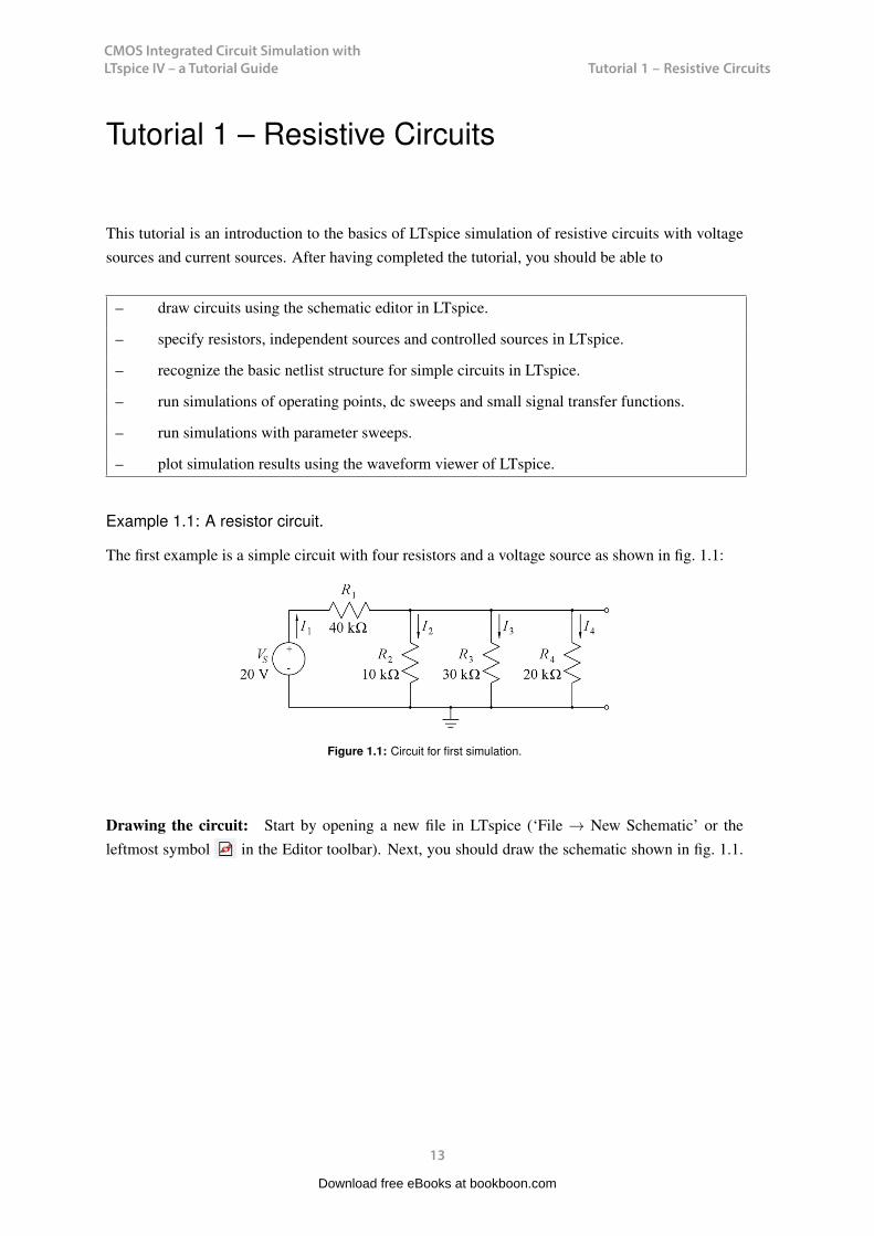
Example 1.1: A resistor circuit.
The first example is a simple circuit with four resistors and a voltage source as shown in fig. 1.1:
Figure 1.1: Circuit for first simulation.
Drawing the circuit: Start by opening a new file in LTspice (‘File → New Schematic’ or theleftmost symbol in the Editor toolbar). Next, you should draw the schematic shown in fig. 1.1.
13
Download free eBooks at bookboon.com

CMOS Integrated Circuit Simulation with LTspice IV – a Tutorial Guide
14
Tutorial 1 – Resistive CircuitsCMOS Integrated Circuit Simulation with LTspice IV Tutorial 1
Figure 1.2: Some toolbar symbols.
Click (left mouse click) on the resistor symbol shown in the toolbar (symbol ) and place the fourresistors. You may rotate a resistor by clicking on the ‘rotate’ symbol on the toolbar or by typing‘Ctrl-R’ when placing the resistor. Right click on the mouse (or type ‘Esc’) to leave the insertioncommand. As an alternative to picking the resistor from the toolbar, you may use the command ‘Edit→ Resistor’, or you may simply type ‘R’. The resistors may now be edited to the correct values andnumbers shown in fig. 1.1. Move the cursor to the resistor number (the reference designator, e.g.R1). On the status bar at the bottom of the LTspice program window, a message will appear, tellingyou that with a right click you can edit the name of the resistor. The right click opens a dialoguebox where you can enter the new reference designator. Likewise, the value of the resistor is editedby right clicking R.
A figure pointing out some of the toolbar symbols is shown in fig. 1.2.
14
Download free eBooks at bookboon.com
Click on the ad to read moreClick on the ad to read moreClick on the ad to read moreClick on the ad to read more
Maersk.com/Mitas
e Graduate Programme for Engineers and Geoscientists
Month 16I was a construction
supervisor in the North Sea
advising and helping foremen
solve problems
I was a
hes
Real work International opportunities
ree work placementsal Internationaorree wo
I wanted real responsibili I joined MITAS because
www.discovermitas.com
CMOS Integrated Circuit Simulation with LTspice IV – a Tutorial Guide
15
Tutorial 1 – Resistive CircuitsCMOS Integrated Circuit Simulation with LTspice IV Tutorial 1
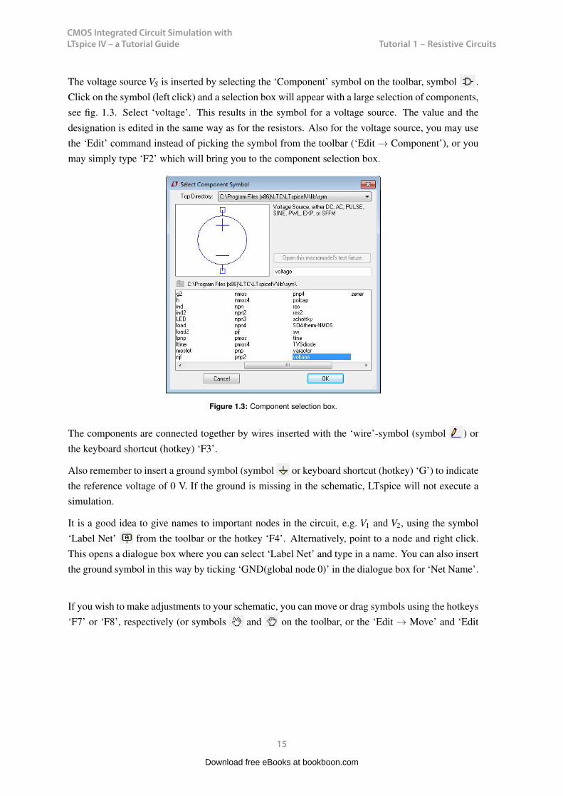
The voltage source VS is inserted by selecting the ‘Component’ symbol on the toolbar, symbol .Click on the symbol (left click) and a selection box will appear with a large selection of components,see fig. 1.3. Select ‘voltage’. This results in the symbol for a voltage source. The value and thedesignation is edited in the same way as for the resistors. Also for the voltage source, you may usethe ‘Edit’ command instead of picking the symbol from the toolbar (‘Edit → Component’), or youmay simply type ‘F2’ which will bring you to the component selection box.
Figure 1.3: Component selection box.
The components are connected together by wires inserted with the ‘wire’-symbol (symbol ) orthe keyboard shortcut (hotkey) ‘F3’.
Also remember to insert a ground symbol (symbol or keyboard shortcut (hotkey) ‘G’) to indicatethe reference voltage of 0 V. If the ground is missing in the schematic, LTspice will not execute asimulation.
It is a good idea to give names to important nodes in the circuit, e.g. V1 and V2, using the symbol‘Label Net’ from the toolbar or the hotkey ‘F4’. Alternatively, point to a node and right click.This opens a dialogue box where you can select ‘Label Net’ and type in a name. You can also insertthe ground symbol in this way by ticking ‘GND(global node 0)’ in the dialogue box for ‘Net Name’.
If you wish to make adjustments to your schematic, you can move or drag symbols using the hotkeys‘F7’ or ‘F8’, respectively (or symbols and on the toolbar, or the ‘Edit → Move’ and ‘Edit
15
Download free eBooks at bookboon.com

CMOS Integrated Circuit Simulation with LTspice IV – a Tutorial Guide
16
Tutorial 1 – Resistive CircuitsCMOS Integrated Circuit Simulation with LTspice IV Tutorial 1
→ Drag’ commands). Also, you can delete a symbol or wire using ‘F5’, toolbar symbol or ‘Edit→ Delete’, and you can duplicate symbols using ‘F6’, toolbar symbol or ‘Edit → Duplicate’.These commands work not only on single symbols. When you have activated one of the commands,you can define a box by clicking and dragging using the left mouse button, and the command willwork on the entire contents of the box.
The assignment of hotkeys can be seen (and edited) using the command ‘Tools → Control Panel →Drafting Options → Hotkeys’.
The resulting schematic may look like the schematic shown in fig. 1.4. When the schematic iscompleted, you should save it (using ‘File → Save as’) in an appropriate folder for your circuitsand using a suitable file name. You can also export the schematic to other programs. A very simplemethod is to use the command ‘Tools → Copy bitmap to Clipboard’ and then paste the schematicinto another program (e.g. Microsoft Word) from the clipboard (using ‘Ctrl-V’).
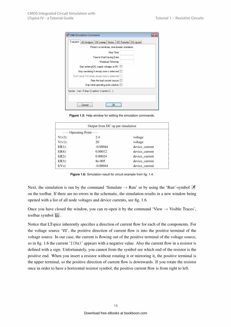
Simulating the circuit: Now the circuit is ready to be simulated. For this, we need a simulationcommand. When selecting the command ‘Simulate → Edit Simulation Cmd’, a window opens witha number of tabs as shown in fig. 1.5 on page 18. Each tab provides help for the basic simulationmodes in LTspice. These are:
16
Download free eBooks at bookboon.com
Click on the ad to read moreClick on the ad to read moreClick on the ad to read moreClick on the ad to read moreClick on the ad to read more
CMOS Integrated Circuit Simulation with LTspice IV – a Tutorial Guide
17
Tutorial 1 – Resistive CircuitsCMOS Integrated Circuit Simulation with LTspice IV Tutorial 1
Transient: Perform a non-linear time domain simulation. This is used for finding voltages andcurrents as function of time, e.g. charging and discharging of a capacitor.
AC Analysis: Compute the small signal AC behavior of the circuit linearized about its DC operatingpoint. This is used for finding the frequency response of a circuit, e.g. the Bode plot of a gainfunction.
DC sweep: Compute the DC operating point of a circuit while stepping independent sources andtreating capacitances as open circuits and inductances as short circuits. This is used for findingvoltages and currents as function of one (or more) signals varying in magnitude, e.g. the outputvoltage of an amplifier as a funtion of the input voltage.
Noise: Perform a stochastic noise analysis of the circuit linearized about its DC operating point.This is used for analyzing the noise performance of a circuit, e.g. finding thermal noise andflicker noise in a gain stage with MOS transistors.
DC Transfer: Find the DC small signal transfer function. This is used for finding small signal inputresistance, output resistance and transfer function for a circuit at DC, i.e. the frequency of theinput signal source is 0.
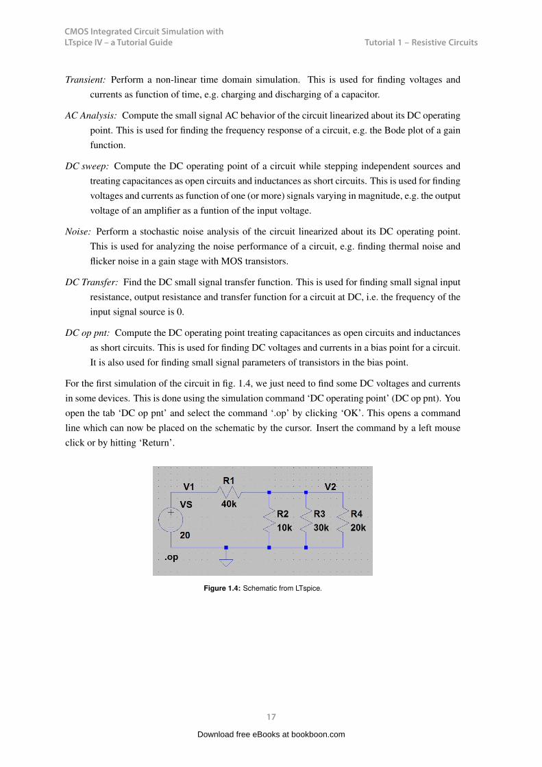
DC op pnt: Compute the DC operating point treating capacitances as open circuits and inductancesas short circuits. This is used for finding DC voltages and currents in a bias point for a circuit.It is also used for finding small signal parameters of transistors in the bias point.
For the first simulation of the circuit in fig. 1.4, we just need to find some DC voltages and currentsin some devices. This is done using the simulation command ‘DC operating point’ (DC op pnt). Youopen the tab ‘DC op pnt’ and select the command ‘.op’ by clicking ‘OK’. This opens a commandline which can now be placed on the schematic by the cursor. Insert the command by a left mouseclick or by hitting ‘Return’.
Figure 1.4: Schematic from LTspice.
17
Download free eBooks at bookboon.com
CMOS Integrated Circuit Simulation with LTspice IV – a Tutorial Guide
18
Tutorial 1 – Resistive CircuitsCMOS Integrated Circuit Simulation with LTspice IV Tutorial 1
Figure 1.5: Help window for editing the simulation commands.
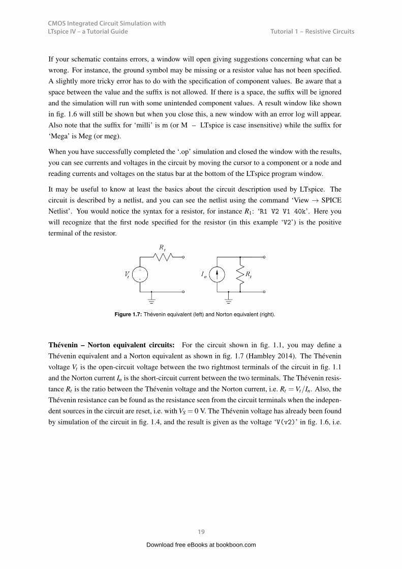
Output from DC op pnt simulation
- - - Operating Point - - -V(v2): 2.4 voltageV(v1): 20 voltageI(R1): -0.00044 device_currentI(R4): 0.00012 device_currentI(R2): 0.00024 device_currentI(R3): 8e-005 device_currentI(Vs): -0.00044 device_current
Figure 1.6: Simulation result for circuit example from fig. 1.4.
Next, the simulation is run by the command ‘Simulate → Run’ or by using the ‘Run’-symbolon the toolbar. If there are no errors in the schematic, the simulation results in a new window beingopened with a list of all node voltages and device currents, see fig. 1.6.
Once you have closed the window, you can re-open it by the command ‘View → Visible Traces’,toolbar symbol .
Notice that LTspice inherently specifies a direction of current flow for each of the components. Forthe voltage source ‘VS’, the positive direction of current flow is into the positive terminal of thevoltage source. In our case, the current is flowing out of the positive terminal of the voltage source,so in fig. 1.6 the current ‘I(Vs)’ appears with a negative value. Also the current flow in a resistor isdefined with a sign. Unfortunately, you cannot from the symbol see which end of the resistor is thepositive end. When you insert a resistor without rotating it or mirroring it, the positive terminal is
18
CMOS Integrated Circuit Simulation with LTspice IV Tutorial 1
the upper terminal, so the positive direction of current flow is downwards. If you rotate the resistoronce in order to have a horizontal resistor symbol, the positive current flow is from right to left.
If your schematic contains errors, a window will open giving suggestions concerning what can bewrong. For instance, the ground symbol may be missing or a resistor value has not been specified.A slightly more tricky error has to do with the specification of component values. Be aware that aspace between the value and the suffix is not allowed. If there is a space, the suffix will be ignoredand the simulation will run with some unintended component values. A result window like shownin fig. 1.6 will still be shown but when you close this, a new window with an error log will appear.Also note that the suffix for ‘milli’ is m (or M – LTspice is case insensitive) while the suffix for‘Mega’ is Meg (or meg).
When you have successfully completed the ‘.op’ simulation and closed the window with the results,you can see currents and voltages in the circuit by moving the cursor to a component or a node andreading currents and voltages on the status bar at the bottom of the LTspice program window.
It may be useful to know at least the basics about the circuit description used by LTspice. Thecircuit is described by a netlist, and you can see the netlist using the command ‘View → SPICENetlist’. You would notice the syntax for a resistor, for instance R1: ‘R1 V2 V1 40k’. Here youwill recognize that the first node specified for the resistor (in this example ‘V2’) is the positiveterminal of the resistor.
Figure 1.7: Thévenin equivalent (left) and Norton equivalent (right).
Thévenin – Norton equivalent circuits: For the circuit shown in fig. 1.1, you may define aThévenin equivalent and a Norton equivalent as shown in fig. 1.7 (Hambley 2014). The Théveninvoltage Vt is the open-circuit voltage between the two rightmost terminals of the circuit in fig. 1.1and the Norton current In is the short-circuit current between the two terminals. The Thévenin resis-tance Rt is the ratio between the Thévenin voltage and the Norton current, i.e. Rt =Vt/In. Also, theThévenin resistance can be found as the resistance seen from the circuit terminals when the indepen-dent sources in the circuit are reset, i.e. with VS = 0 V. The Thévenin voltage has already been foundby simulation of the circuit in fig. 1.4, and the result is given as the voltage ‘V(v2)’ in fig. 1.6, i.e.
19
Download free eBooks at bookboon.com
CMOS Integrated Circuit Simulation with LTspice IV – a Tutorial Guide
19
Tutorial 1 – Resistive Circuits
CMOS Integrated Circuit Simulation with LTspice IV Tutorial 1
the upper terminal, so the positive direction of current flow is downwards. If you rotate the resistoronce in order to have a horizontal resistor symbol, the positive current flow is from right to left.
If your schematic contains errors, a window will open giving suggestions concerning what can bewrong. For instance, the ground symbol may be missing or a resistor value has not been specified.A slightly more tricky error has to do with the specification of component values. Be aware that aspace between the value and the suffix is not allowed. If there is a space, the suffix will be ignoredand the simulation will run with some unintended component values. A result window like shownin fig. 1.6 will still be shown but when you close this, a new window with an error log will appear.Also note that the suffix for ‘milli’ is m (or M – LTspice is case insensitive) while the suffix for‘Mega’ is Meg (or meg).
When you have successfully completed the ‘.op’ simulation and closed the window with the results,you can see currents and voltages in the circuit by moving the cursor to a component or a node andreading currents and voltages on the status bar at the bottom of the LTspice program window.
It may be useful to know at least the basics about the circuit description used by LTspice. Thecircuit is described by a netlist, and you can see the netlist using the command ‘View → SPICENetlist’. You would notice the syntax for a resistor, for instance R1: ‘R1 V2 V1 40k’. Here youwill recognize that the first node specified for the resistor (in this example ‘V2’) is the positiveterminal of the resistor.
Figure 1.7: Thévenin equivalent (left) and Norton equivalent (right).
Thévenin – Norton equivalent circuits: For the circuit shown in fig. 1.1, you may define aThévenin equivalent and a Norton equivalent as shown in fig. 1.7 (Hambley 2014). The Théveninvoltage Vt is the open-circuit voltage between the two rightmost terminals of the circuit in fig. 1.1and the Norton current In is the short-circuit current between the two terminals. The Thévenin resis-tance Rt is the ratio between the Thévenin voltage and the Norton current, i.e. Rt =Vt/In. Also, theThévenin resistance can be found as the resistance seen from the circuit terminals when the indepen-dent sources in the circuit are reset, i.e. with VS = 0 V. The Thévenin voltage has already been foundby simulation of the circuit in fig. 1.4, and the result is given as the voltage ‘V(v2)’ in fig. 1.6, i.e.
19
Download free eBooks at bookboon.com

CMOS Integrated Circuit Simulation with LTspice IV – a Tutorial Guide
20
Tutorial 1 – Resistive CircuitsCMOS Integrated Circuit Simulation with LTspice IV Tutorial 1
Vt = 2.4 V. The short-circuit current is found by placing a short-circuit between the two rightmostterminals in the circuit. The short-circuit could simply be a wire, but in this case, the current in thewire is not listed in the output file from the ‘.op’ simulation. You may also try to insert a resistor withthe value 0, but running the simulation, you will find that the output file does not show the value ofthe current in this resistor. You may change the resistor value to a very small value (e.g. 1e-6), andin this case, the output file will show the current in the short-circuit resistor. Alternatively, you canmodel the short-circuit by a voltage source with a value of 0 V. In this case, the output file will showthe current into the voltage source, and the voltage between the two terminals is 0 V, correspondingto a short-circuit. When running this simulation, you will find In = 0.5 mA, and you can calculateRt from Rt = Vt/In = 4.8 kΩ. Alternatively, Rt can be found by simulation: Insert a current sourceI1 between the two rightmost terminals and simulate the voltage V2 across the current source withVS = 0 V. The current source is inserted as a component where you select ‘current’ in the componentselection window. With the current flowing into the V2 terminal (rotate the current source symboltwice), the resistance is found as V2/I1, so if I1 is selected to be 1, the value of the voltage V2 isdirectly the value of the resistance between the terminals, i.e. Rt .
Annotating simulation results on the schematic: After having run a ‘.op’ simulation, you maywish to display the simulation results directly on the schematic. Consider the circuit from fig. 1.4.For this circuit, we found the results shown in fig. 1.6. A very simple way to show these results on
20
Download free eBooks at bookboon.com
Click on the ad to read moreClick on the ad to read moreClick on the ad to read moreClick on the ad to read moreClick on the ad to read moreClick on the ad to read more
STUDY AT A TOP RANKED INTERNATIONAL BUSINESS SCHOOL
Reach your full potential at the Stockholm School of Economics, in one of the most innovative cities in the world. The School is ranked by the Financial Times as the number one business school in the Nordic and Baltic countries.
Visit us at www.hhs.se
Swed
en
Stockholm
no.1nine years in a row
CMOS Integrated Circuit Simulation with LTspice IV – a Tutorial Guide
21
Tutorial 1 – Resistive Circuits
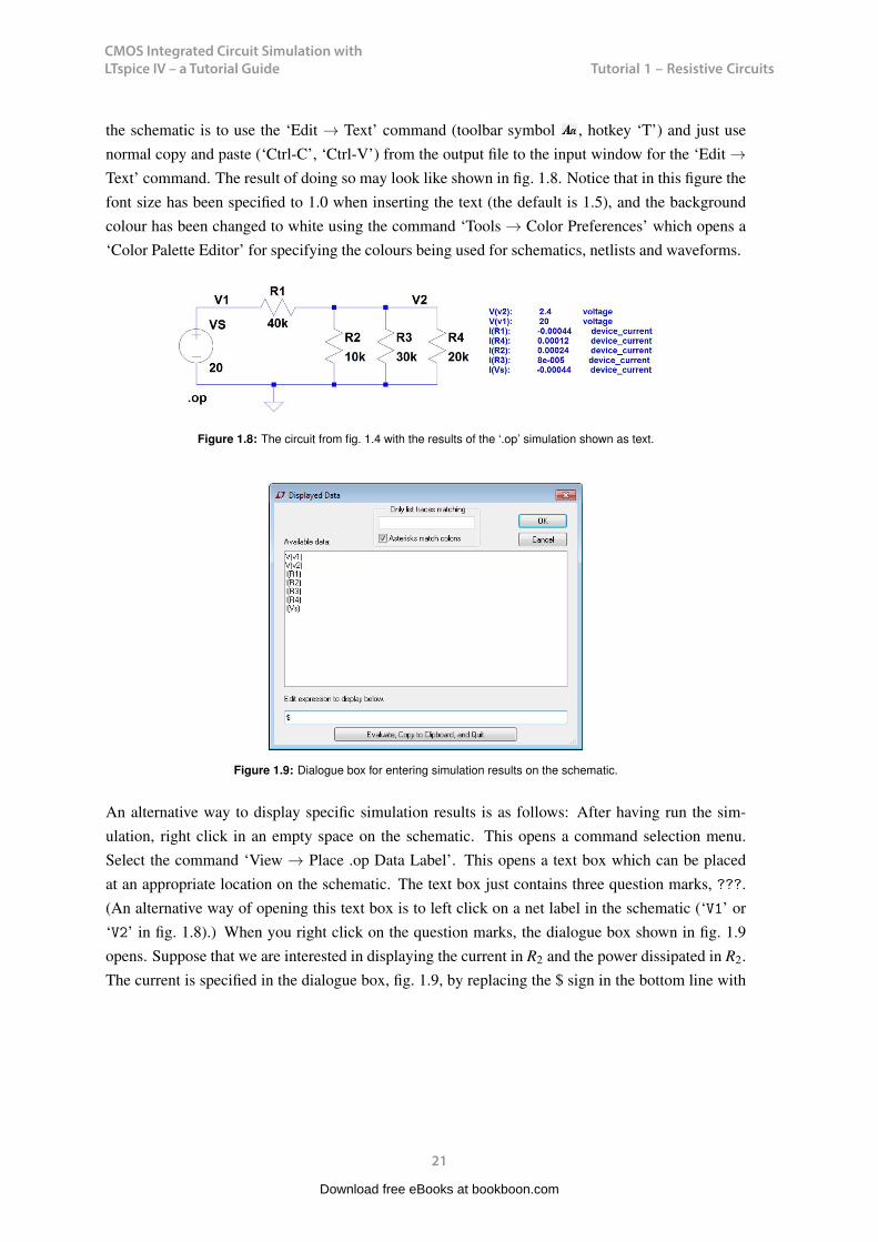
the schematic is to use the ‘Edit → Text’ command (toolbar symbol , hotkey ‘T’) and just usenormal copy and paste (‘Ctrl-C’, ‘Ctrl-V’) from the output file to the input window for the ‘Edit →Text’ command. The result of doing so may look like shown in fig. 1.8. Notice that in this figure thefont size has been specified to 1.0 when inserting the text (the default is 1.5), and the backgroundcolour has been changed to white using the command ‘Tools → Color Preferences’ which opens a‘Color Palette Editor’ for specifying the colours being used for schematics, netlists and waveforms.
Figure 1.8: The circuit from fig. 1.4 with the results of the ‘.op’ simulation shown as text.
Figure 1.9: Dialogue box for entering simulation results on the schematic.
An alternative way to display specific simulation results is as follows: After having run the sim-ulation, right click in an empty space on the schematic. This opens a command selection menu.Select the command ‘View → Place .op Data Label’. This opens a text box which can be placedat an appropriate location on the schematic. The text box just contains three question marks, ???.(An alternative way of opening this text box is to left click on a net label in the schematic (‘V1’ or‘V2’ in fig. 1.8).) When you right click on the question marks, the dialogue box shown in fig. 1.9opens. Suppose that we are interested in displaying the current in R2 and the power dissipated in R2.The current is specified in the dialogue box, fig. 1.9, by replacing the $ sign in the bottom line with
Download free eBooks at bookboon.com

CMOS Integrated Circuit Simulation with LTspice IV – a Tutorial Guide
22
Tutorial 1 – Resistive CircuitsCMOS Integrated Circuit Simulation with LTspice IV Tutorial 1
(a) (b)
Figure 1.10: The circuit from fig. 1.4 with the current and the power for R2 shown on the schematic.
‘I(R2)’. Adding a new text box in the same way lets you specify the expression ‘I(R2)*V(v2)’which will calculate the power in R2. The resulting schematic may look like shown in fig. 1.10(a).You may find that the current and power need rounding off to integer µA and µW. This can beachieved using the function ‘round(x)’ in the specification window. Thus, for the current specify‘round(I(R2)*1e6)/1e6’ and for the power specify ‘round(I(R2)*V(v2)*1e6)/1e6’. Then theresulting schematic looks like shown in fig. 1.10(b).
Sweeping DC voltages and currents: The simulations just shown give you values of voltagesand currents in a specific operating point, i.e. for fixed values of all components in the system.
22
Download free eBooks at bookboon.com
Click on the ad to read moreClick on the ad to read moreClick on the ad to read moreClick on the ad to read moreClick on the ad to read moreClick on the ad to read moreClick on the ad to read more
CMOS Integrated Circuit Simulation with LTspice IV – a Tutorial Guide
23
Tutorial 1 – Resistive CircuitsCMOS Integrated Circuit Simulation with LTspice IV Tutorial 1
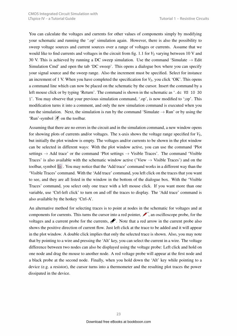
You can calculate the voltages and currents for other values of components simply by modifyingyour schematic and running the ‘.op’ simulation again. However, there is also the possibility tosweep voltage sources and current sources over a range of voltages or currents. Assume that wewould like to find currents and voltages in the circuit from fig. 1.1 for VS varying between 10 V and30 V. This is achieved by running a DC sweep simulation. Use the command ‘Simulate → EditSimulation Cmd’ and open the tab ‘DC sweep’. This opens a dialogue box where you can specifyyour signal source and the sweep range. Also the increment must be specified. Select for instancean increment of 1 V. When you have completed the specification for VS, you click ‘OK’. This opensa command line which can now be placed on the schematic by the cursor. Insert the command by aleft mouse click or by typing ‘Return’. The command is shown in the schematic as ‘.dc VS 10 30
1’. You may observe that your previous simulation command, ‘.op’, is now modified to ‘;op’. Thismodification turns it into a comment, and only the new simulation command is executed when yourun the simulation. Next, the simulation is run by the command ‘Simulate → Run’ or by using the‘Run’-symbol on the toolbar.
Assuming that there are no errors in the circuit and in the simulation command, a new window opensfor showing plots of currents and/or voltages. The x-axis shows the voltage range specified for VS,but initially the plot window is empty. The voltages and/or currents to be shown in the plot windowcan be selected in different ways: With the plot window active, you can use the command ‘Plotsettings → Add trace’ or the command ‘Plot settings → Visible Traces’. The command ‘VisibleTraces’ is also available with the schematic window active (’View → Visible Traces’) and on thetoolbar, symbol . You may notice that the ‘Add trace’ command works in a different way than the‘Visible Traces’ command. With the ‘Add trace’ command, you left click on the traces that you wantto see, and they are all listed in the window in the bottom of the dialogue box. With the ‘VisibleTraces’ command, you select only one trace with a left mouse click. If you want more than onevariable, use ‘Ctrl-left click’ to turn on and off the traces to display. The ‘Add trace’ command isalso available by the hotkey ‘Ctrl-A’.
An alternative method for selecting traces is to point at nodes in the schematic for voltages and atcomponents for currents. This turns the cursor into a red pointer, , an oscilloscope probe, for thevoltages and a current probe for the currents, . Note that a red arrow in the current probe alsoshows the positive direction of current flow. Just left click at the trace to be added and it will appearin the plot window. A double click implies that only the selected trace is shown. Also, you may notethat by pointing to a wire and pressing the ‘Alt’ key, you can select the current in a wire. The voltagedifference between two nodes can also be displayed using the voltage probe: Left click and hold onone node and drag the mouse to another node. A red voltage probe will appear at the first node anda black probe at the second node. Finally, when you hold down the ‘Alt’ key while pointing to a
23
CMOS Integrated Circuit Simulation with LTspice IV Tutorial 1
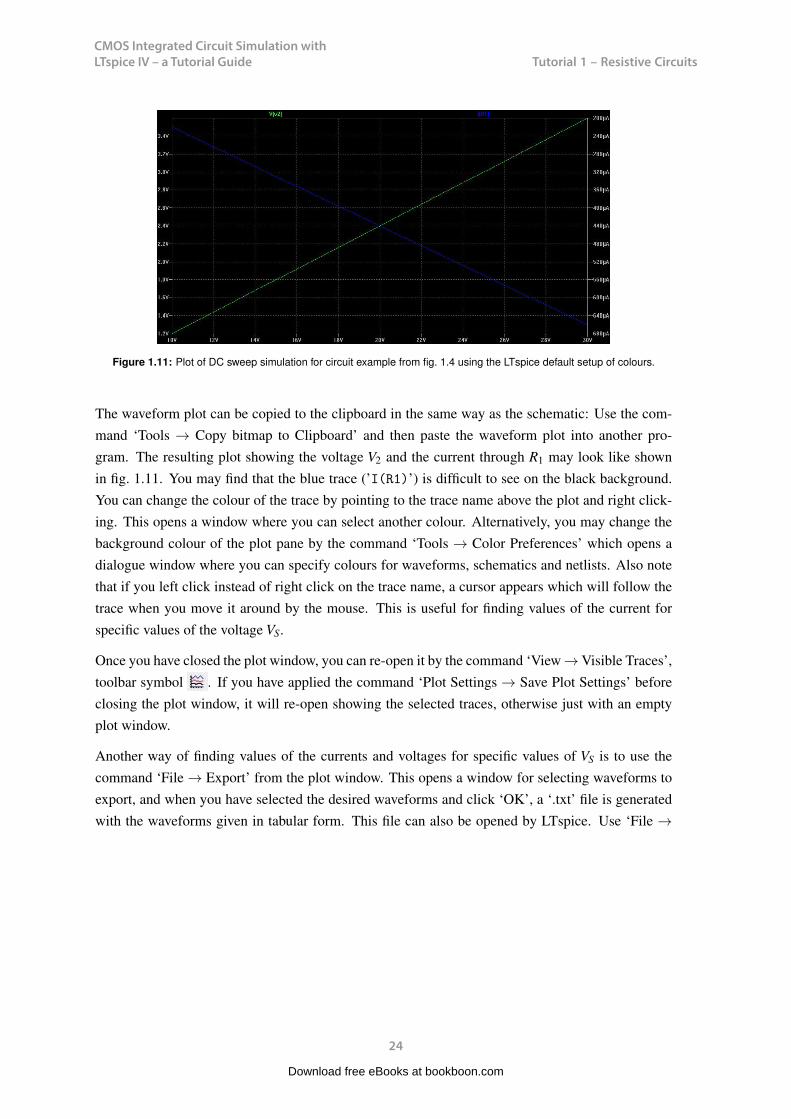
Figure 1.11: Plot of DC sweep simulation for circuit example from fig. 1.4 using the LTspice default setup of colours.
device (e.g. a resistor), the cursor turns into a thermometer and the resulting plot traces the powerdissipated in the device.
The waveform plot can be copied to the clipboard in the same way as the schematic: Use the com-mand ‘Tools → Copy bitmap to Clipboard’ and then paste the waveform plot into another pro-gram. The resulting plot showing the voltage V2 and the current through R1 may look like shownin fig. 1.11. You may find that the blue trace (’I(R1)’) is difficult to see on the black background.You can change the colour of the trace by pointing to the trace name above the plot and right click-ing. This opens a window where you can select another colour. Alternatively, you may change thebackground colour of the plot pane by the command ‘Tools → Color Preferences’ which opens adialogue window where you can specify colours for waveforms, schematics and netlists. Also notethat if you left click instead of right click on the trace name, a cursor appears which will follow thetrace when you move it around by the mouse. This is useful for finding values of the current forspecific values of the voltage VS.
Once you have closed the plot window, you can re-open it by the command ‘View → Visible Traces’,toolbar symbol . If you have applied the command ‘Plot Settings → Save Plot Settings’ beforeclosing the plot window, it will re-open showing the selected traces, otherwise just with an emptyplot window.
Another way of finding values of the currents and voltages for specific values of VS is to use thecommand ‘File → Export’ from the plot window. This opens a window for selecting waveforms toexport, and when you have selected the desired waveforms and click ‘OK’, a ‘.txt’ file is generatedwith the waveforms given in tabular form. This file can also be opened by LTspice. Use ‘File →
24
Download free eBooks at bookboon.com
CMOS Integrated Circuit Simulation with LTspice IV – a Tutorial Guide
24
Tutorial 1 – Resistive CircuitsCMOS Integrated Circuit Simulation with LTspice IV Tutorial 1
Figure 1.11: Plot of DC sweep simulation for circuit example from fig. 1.4 using the LTspice default setup of colours.
device (e.g. a resistor), the cursor turns into a thermometer and the resulting plot traces the powerdissipated in the device.
The waveform plot can be copied to the clipboard in the same way as the schematic: Use the com-mand ‘Tools → Copy bitmap to Clipboard’ and then paste the waveform plot into another pro-gram. The resulting plot showing the voltage V2 and the current through R1 may look like shownin fig. 1.11. You may find that the blue trace (’I(R1)’) is difficult to see on the black background.You can change the colour of the trace by pointing to the trace name above the plot and right click-ing. This opens a window where you can select another colour. Alternatively, you may change thebackground colour of the plot pane by the command ‘Tools → Color Preferences’ which opens adialogue window where you can specify colours for waveforms, schematics and netlists. Also notethat if you left click instead of right click on the trace name, a cursor appears which will follow thetrace when you move it around by the mouse. This is useful for finding values of the current forspecific values of the voltage VS.
Once you have closed the plot window, you can re-open it by the command ‘View → Visible Traces’,toolbar symbol . If you have applied the command ‘Plot Settings → Save Plot Settings’ beforeclosing the plot window, it will re-open showing the selected traces, otherwise just with an emptyplot window.
Another way of finding values of the currents and voltages for specific values of VS is to use thecommand ‘File → Export’ from the plot window. This opens a window for selecting waveforms toexport, and when you have selected the desired waveforms and click ‘OK’, a ‘.txt’ file is generatedwith the waveforms given in tabular form. This file can also be opened by LTspice. Use ‘File →
24
CMOS Integrated Circuit Simulation with LTspice IV Tutorial 1
Figure 1.11: Plot of DC sweep simulation for circuit example from fig. 1.4 using the LTspice default setup of colours.
device (e.g. a resistor), the cursor turns into a thermometer and the resulting plot traces the powerdissipated in the device.
The waveform plot can be copied to the clipboard in the same way as the schematic: Use the com-mand ‘Tools → Copy bitmap to Clipboard’ and then paste the waveform plot into another pro-gram. The resulting plot showing the voltage V2 and the current through R1 may look like shownin fig. 1.11. You may find that the blue trace (’I(R1)’) is difficult to see on the black background.You can change the colour of the trace by pointing to the trace name above the plot and right click-ing. This opens a window where you can select another colour. Alternatively, you may change thebackground colour of the plot pane by the command ‘Tools → Color Preferences’ which opens adialogue window where you can specify colours for waveforms, schematics and netlists. Also notethat if you left click instead of right click on the trace name, a cursor appears which will follow thetrace when you move it around by the mouse. This is useful for finding values of the current forspecific values of the voltage VS.
Once you have closed the plot window, you can re-open it by the command ‘View → Visible Traces’,toolbar symbol . If you have applied the command ‘Plot Settings → Save Plot Settings’ beforeclosing the plot window, it will re-open showing the selected traces, otherwise just with an emptyplot window.
Another way of finding values of the currents and voltages for specific values of VS is to use thecommand ‘File → Export’ from the plot window. This opens a window for selecting waveforms toexport, and when you have selected the desired waveforms and click ‘OK’, a ‘.txt’ file is generatedwith the waveforms given in tabular form. This file can also be opened by LTspice. Use ‘File →
24
Download free eBooks at bookboon.com
CMOS Integrated Circuit Simulation with LTspice IV – a Tutorial Guide
25
Tutorial 1 – Resistive CircuitsCMOS Integrated Circuit Simulation with LTspice IV Tutorial 1
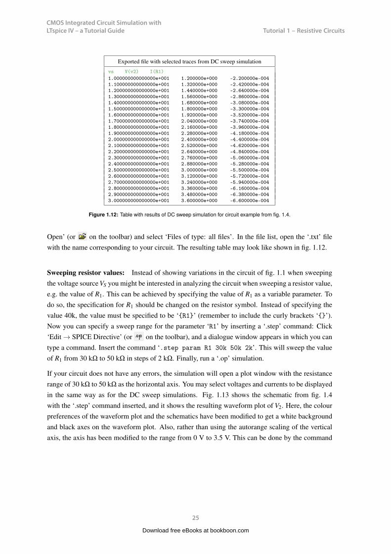
Exported file with selected traces from DC sweep simulation
vs V(v2) I(R1)1.000000000000000e+001 1.200000e+000 -2.200000e-0041.100000000000000e+001 1.320000e+000 -2.420000e-0041.200000000000000e+001 1.440000e+000 -2.640000e-0041.300000000000000e+001 1.560000e+000 -2.860000e-0041.400000000000000e+001 1.680000e+000 -3.080000e-0041.500000000000000e+001 1.800000e+000 -3.300000e-0041.600000000000000e+001 1.920000e+000 -3.520000e-0041.700000000000000e+001 2.040000e+000 -3.740000e-0041.800000000000000e+001 2.160000e+000 -3.960000e-0041.900000000000000e+001 2.280000e+000 -4.180000e-0042.000000000000000e+001 2.400000e+000 -4.400000e-0042.100000000000000e+001 2.520000e+000 -4.620000e-0042.200000000000000e+001 2.640000e+000 -4.840000e-0042.300000000000000e+001 2.760000e+000 -5.060000e-0042.400000000000000e+001 2.880000e+000 -5.280000e-0042.500000000000000e+001 3.000000e+000 -5.500000e-0042.600000000000000e+001 3.120000e+000 -5.720000e-0042.700000000000000e+001 3.240000e+000 -5.940000e-0042.800000000000000e+001 3.360000e+000 -6.160000e-0042.900000000000000e+001 3.480000e+000 -6.380000e-0043.000000000000000e+001 3.600000e+000 -6.600000e-004
Figure 1.12: Table with results of DC sweep simulation for circuit example from fig. 1.4.
Open’ (or on the toolbar) and select ‘Files of type: all files’. In the file list, open the ‘.txt’ filewith the name corresponding to your circuit. The resulting table may look like shown in fig. 1.12.
Sweeping resistor values: Instead of showing variations in the circuit of fig. 1.1 when sweepingthe voltage source VS you might be interested in analyzing the circuit when sweeping a resistor value,e.g. the value of R1. This can be achieved by specifying the value of R1 as a variable parameter. Todo so, the specification for R1 should be changed on the resistor symbol. Instead of specifying thevalue 40k, the value must be specified to be ‘R1’ (remember to include the curly brackets ‘’).Now you can specify a sweep range for the parameter ‘R1’ by inserting a ‘.step’ command: Click‘Edit → SPICE Directive’ (or on the toolbar), and a dialogue window appears in which you cantype a command. Insert the command ‘.step param R1 30k 50k 2k’. This will sweep the valueof R1 from 30 kΩ to 50 kΩ in steps of 2 kΩ. Finally, run a ‘.op’ simulation.
If your circuit does not have any errors, the simulation will open a plot window with the resistancerange of 30 kΩ to 50 kΩ as the horizontal axis. You may select voltages and currents to be displayedin the same way as for the DC sweep simulations. Fig. 1.13 shows the schematic from fig. 1.4with the ‘.step’ command inserted, and it shows the resulting waveform plot of V2. Here, the colourpreferences of the waveform plot and the schematics have been modified to get a white backgroundand black axes on the waveform plot. Also, rather than using the autorange scaling of the verticalaxis, the axis has been modified to the range from 0 V to 3.5 V. This can be done by the command
25
Download free eBooks at bookboon.com

CMOS Integrated Circuit Simulation with LTspice IV – a Tutorial Guide
26
Tutorial 1 – Resistive CircuitsCMOS Integrated Circuit Simulation with LTspice IV Tutorial 1
Figure 1.13: Simulation of sweep of resistor R1 from fig. 1.1.
‘Plot settings → Manual Limits’ or by moving the mouse cursor over the axis and left clicking. Infig. 1.13 (and in subsequent figures showing simulation plots), the font size of the labels on the axeshas been increased using the command ‘Tools → Control Panel’ and the tab ‘Waveforms’ where thefont has been changed to Arial and the fontsize to 18 points.
In a waveform plot, you can insert text and other annotations (e.g. cursor position) using the com-mand ‘Plot Settings → Notes & Annotations’.
In the plot window, you can also zoom in on details simply by clicking and dragging to define a boxusing the left mouse button.
26
Download free eBooks at bookboon.com
Click on the ad to read moreClick on the ad to read moreClick on the ad to read moreClick on the ad to read moreClick on the ad to read moreClick on the ad to read moreClick on the ad to read moreClick on the ad to read more
CMOS Integrated Circuit Simulation with LTspice IV – a Tutorial Guide
27
Tutorial 1 – Resistive CircuitsCMOS Integrated Circuit Simulation with LTspice IV Tutorial 1
If you want to run a simulation with just one value for a variable parameter (R1 in fig. 1.13), theninstead of the ‘.step’ command, you can specify the value of R1 using a ‘.param’ command: Insertthe SPICE Directive ‘.param R1=40k’ to run a simulation with R1 = 40 kΩ and delete the ‘.step’command or edit it into a comment by inserting an asterix (*) as the first character or by ticking‘Comment’ in the editing window. If you do not disable the ‘.step’ command, the simulation willrun this command regardless of the ‘.param’ specification.
The ‘.step param’ command is a very useful command for design iterations. By defining relevantdesign parameters as variable parameters and stepping the values over a suitable range, you canquickly examine the influence of a parameter on the circuit characteristics. Problems 1.2 on page 38and 1.5 on page 39 are examples of this.
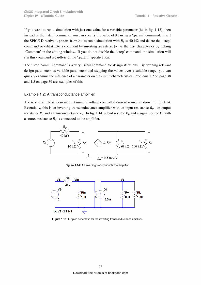
Example 1.2: A transconductance amplifier.
The next example is a circuit containing a voltage controlled current source as shown in fig. 1.14.Essentially, this is an inverting transconductance amplifier with an input resistance Rin, an outputresistance Ro and a transconductance gm. In fig. 1.14, a load resistor RL and a signal source VS witha source resistance RS is connected to the amplifier.
Figure 1.14: An inverting transconductance amplifier.
Figure 1.15: LTspice schematic for the inverting transconductance amplifier.
27
Download free eBooks at bookboon.com

CMOS Integrated Circuit Simulation with LTspice IV – a Tutorial Guide
28
Tutorial 1 – Resistive CircuitsCMOS Integrated Circuit Simulation with LTspice IV Tutorial 1
In this circuit, there is a new type of component, the controlled current source. LTspice has, likeother Spice programs (Tuinenga 1995; Vladimirescu 1994), a voltage controlled current source asa standard component with the circuit designator G. The schematic drawn in LTspice is shown infig. 1.15. The LTspice symbol for the controlled current source explicitly shows the controllingvoltage as input terminals to the component symbol. The controlled current source is edited by rightclicking on the symbol. This opens a ‘Component Attribute Editor’ as shown in fig. 1.16. By doubleclicking on the values for ‘InstName’ and ‘Value’, the values can be changed to the values shown infig. 1.15. Alternatively, just right click on the device number (e.g. G1) and the value G to edit them
Figure 1.16: The window for editing the specifications of the voltage controlled current source.
28
Download free eBooks at bookboon.com
Click on the ad to read moreClick on the ad to read moreClick on the ad to read moreClick on the ad to read moreClick on the ad to read moreClick on the ad to read moreClick on the ad to read moreClick on the ad to read moreClick on the ad to read more
“The perfect start of a successful, international career.”
CLICK HERE to discover why both socially
and academically the University
of Groningen is one of the best
places for a student to be www.rug.nl/feb/education
Excellent Economics and Business programmes at:
CMOS Integrated Circuit Simulation with LTspice IV – a Tutorial Guide
29
Tutorial 1 – Resistive CircuitsCMOS Integrated Circuit Simulation with LTspice IV Tutorial 1
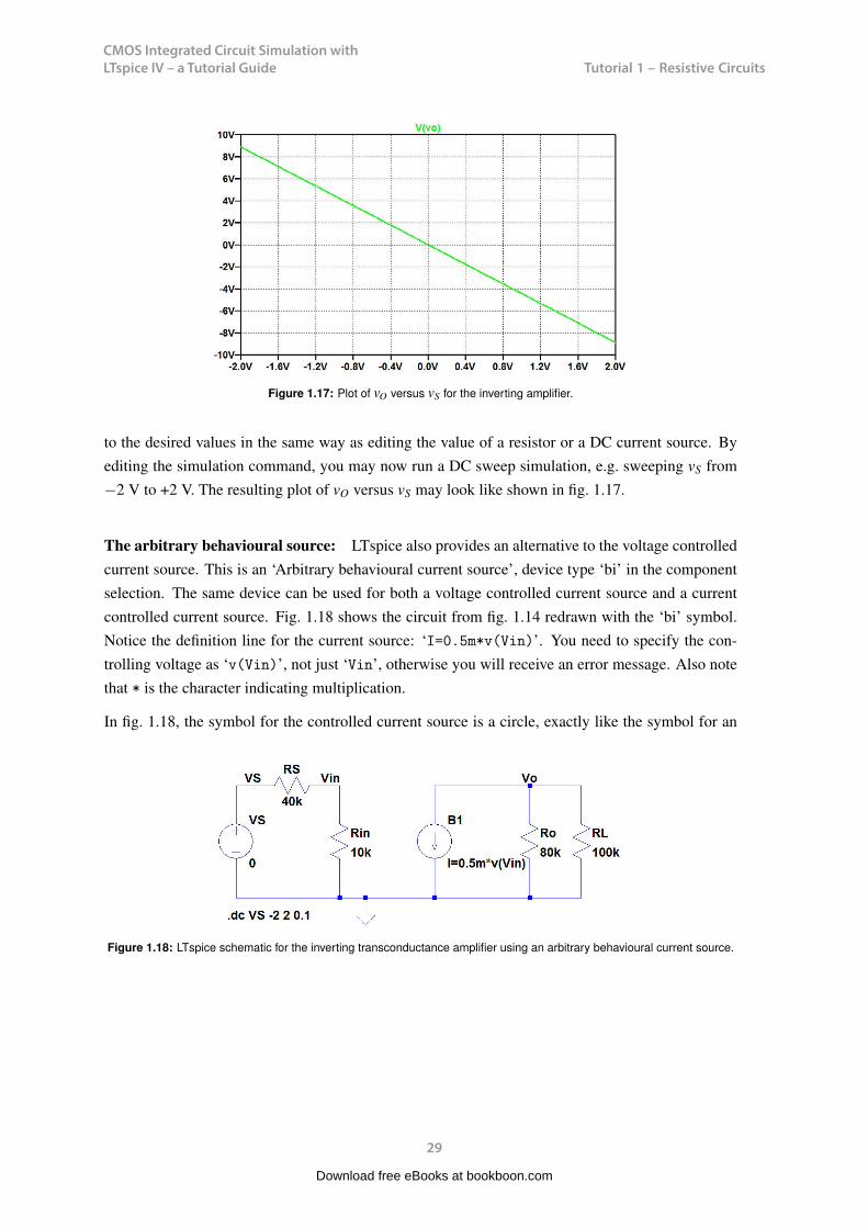
Figure 1.17: Plot of vO versus vS for the inverting amplifier.
to the desired values in the same way as editing the value of a resistor or a DC current source. Byediting the simulation command, you may now run a DC sweep simulation, e.g. sweeping vS from−2 V to +2 V. The resulting plot of vO versus vS may look like shown in fig. 1.17.
The arbitrary behavioural source: LTspice also provides an alternative to the voltage controlledcurrent source. This is an ‘Arbitrary behavioural current source’, device type ‘bi’ in the componentselection. The same device can be used for both a voltage controlled current source and a currentcontrolled current source. Fig. 1.18 shows the circuit from fig. 1.14 redrawn with the ‘bi’ symbol.Notice the definition line for the current source: ‘I=0.5m*v(Vin)’. You need to specify the con-trolling voltage as ‘v(Vin)’, not just ‘Vin’, otherwise you will receive an error message. Also notethat * is the character indicating multiplication.
In fig. 1.18, the symbol for the controlled current source is a circle, exactly like the symbol for an
Figure 1.18: LTspice schematic for the inverting transconductance amplifier using an arbitrary behavioural current source.
29
Download free eBooks at bookboon.com
CMOS Integrated Circuit Simulation with LTspice IV – a Tutorial Guide
30
Tutorial 1 – Resistive CircuitsCMOS Integrated Circuit Simulation with LTspice IV Tutorial 1
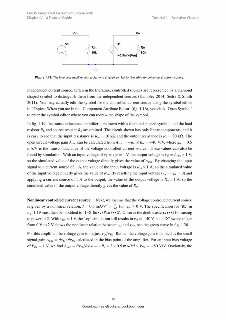
Figure 1.19: The inverting amplifier with a diamond shaped symbol for the arbitrary behavioural current source.
independent current source. Often in the literature, controlled sources are represented by a diamondshaped symbol to distinguish them from the independent sources (Hambley 2014; Sedra & Smith2011). You may actually edit the symbol for the controlled current source using the symbol editorin LTspice. When you are in the ‘Component Attribute Editor’ (fig. 1.16), you click ‘Open Symbol’to enter the symbol editor where you can redraw the shape of the symbol.
In fig. 1.19, the transconductance amplifier is redrawn with a diamond shaped symbol, and the loadresistor RL and source resistor RS are omitted. The circuit shown has only linear components, and itis easy to see that the input resistance is Rin = 10 kΩ and the output resistance is Ro = 80 kΩ. Theopen circuit voltage gain Avoc can be calculated from Avoc =−gm ×Ro =−40 V/V, where gm = 0.5mA/V is the transconductance of the voltage controlled current source. These values can also befound by simulation: With an input voltage of vS = vIN = 1 V, the output voltage is vO = Avoc ×1 V,so the simulated value of the output voltage directly gives the value of Avoc. By changing the inputsignal to a current source of 1 A, the value of the input voltage is Rin ×1 A, so the simulated valueof the input voltage directly gives the value of Rin. By resetting the input voltage (vS = vIN = 0) andapplying a current source of 1 A to the output, the value of the output voltage is Ro × 1 A, so thesimulated value of the output voltage directly gives the value of Ro.
Nonlinear controlled current source: Next, we assume that the voltage controlled current sourceis given by a nonlinear relation, I = 0.5 mA/V2 × v2
IN for vIN ≥ 0 V. The specification for ‘B1’ infig. 1.19 must then be modified to ‘I=0.5m*v(Vin)**2’. Observe the double asterix (**) for raisingto power of 2. With vIN = 1 V, the ‘.op’ simulation still results in vO =−40 V, but a DC sweep of vIN
from 0 V to 2 V shows the nonlinear relation between vO and vIN , see the green curve in fig. 1.20.
For this amplifier, the voltage gain is not just vO/vIN . Rather, the voltage gain is defined as the smallsignal gain Avoc = ∂vO/∂vIN calculated in the bias point of the amplifier. For an input bias voltageof VIN = 1 V, we find Avoc = ∂vO/∂vIN = −Ro ×2×0.5 mA/V2 ×VIN = −80 V/V. Obviously, the
30
Download free eBooks at bookboon.com

CMOS Integrated Circuit Simulation with LTspice IV – a Tutorial Guide
31
Tutorial 1 – Resistive CircuitsCMOS Integrated Circuit Simulation with LTspice IV Tutorial 1
Figure 1.20: Plot of vO versus vS for the inverting amplifier with a nonlinear voltage controlled current source.
gain depends on the bias value of the input voltage. The voltage gain is also seen as the slope ofthe nonlinear relation between vO and vIN . This slope can be displayed directly in the plot window:When you click on the command ‘Plot Settings → Add trace’ (or hotkey ‘Ctrl-A’), a window opensfor specifying traces to plot. The bottom line in this window lets you enter an expression to add. Alarge selection of mathematical operations is available (see the ‘Help’ menu), including the deriva-tive of a variable with respect to the x-axis variable. The function ‘d(V(vo))’ will give you thederivative of the output voltage with respect to the input voltage. The resulting plot is the blue linein fig. 1.20 from which you can see that Avoc =−80 V/V as expected for VIN = 1 V.
31
Download free eBooks at bookboon.com
Click on the ad to read moreClick on the ad to read moreClick on the ad to read moreClick on the ad to read moreClick on the ad to read moreClick on the ad to read moreClick on the ad to read moreClick on the ad to read moreClick on the ad to read moreClick on the ad to read more
89,000 kmIn the past four years we have drilled
That’s more than twice around the world.
careers.slb.com
What will you be?
1 Based on Fortune 500 ranking 2011. Copyright © 2015 Schlumberger. All rights reserved.
Who are we?We are the world’s largest oilfield services company1. Working globally—often in remote and challenging locations— we invent, design, engineer, and apply technology to help our customers find and produce oil and gas safely.
Who are we looking for?Every year, we need thousands of graduates to begin dynamic careers in the following domains:n Engineering, Research and Operationsn Geoscience and Petrotechnicaln Commercial and Business
CMOS Integrated Circuit Simulation with LTspice IV – a Tutorial Guide
32
Tutorial 1 – Resistive CircuitsCMOS Integrated Circuit Simulation with LTspice IV Tutorial 1
Output from DC Transfer simulation
- - - Transfer Function - - -Transfer_function: -80 transfervs#Input_impedance: 10000 impedanceoutput_impedance_at_V(vo): 80000 impedance
Figure 1.21: Output from ‘.tf’ simulation of the circuit from fig. 1.19.
LTspice has another simulation command which will directly give you the small signal transferfunction at DC, the ‘DC Transfer’ simulation. Use the command ‘Simulate → Edit SimulationCommand’ and choose the tab ‘DC Transfer’. Here you specify the output and the source. For thecircuit of fig. 1.19, the output is ‘v(Vo)’ (not just ‘Vo’) and the source is ‘VS’. The resulting simula-tion command is ‘.tf v(Vo) VS’ and after running the simulation (with ‘I=0.5m*v(Vin)**2’), awindow opens with the information shown in fig. 1.21.
Example 1.3: A current amplifier.
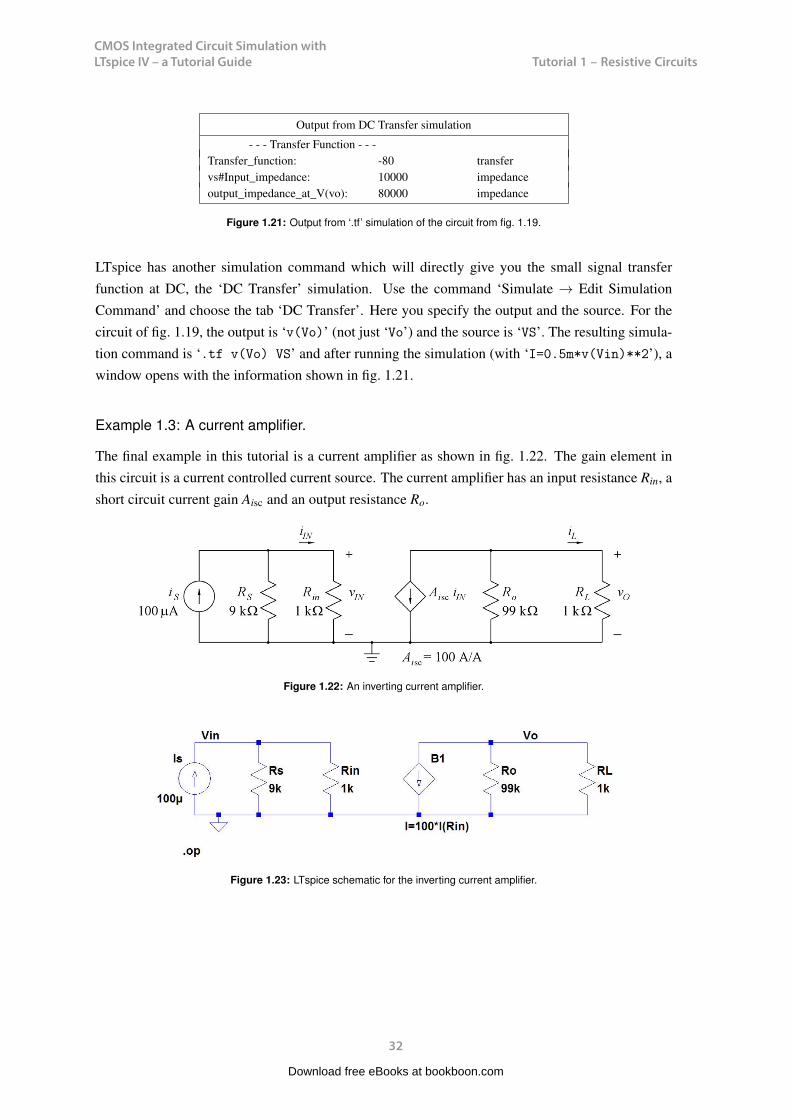
The final example in this tutorial is a current amplifier as shown in fig. 1.22. The gain element inthis circuit is a current controlled current source. The current amplifier has an input resistance Rin, ashort circuit current gain Aisc and an output resistance Ro.
Figure 1.22: An inverting current amplifier.
Figure 1.23: LTspice schematic for the inverting current amplifier.
32
Download free eBooks at bookboon.com
CMOS Integrated Circuit Simulation with LTspice IV – a Tutorial Guide
33
Tutorial 1 – Resistive CircuitsCMOS Integrated Circuit Simulation with LTspice IV Tutorial 1
A simple examination of the circuit shows an inverting current gain from the input signal iS to thecurrent iL in the load resistor of Aisc multiplied by the current divider ratios at the input side and theoutput side. With the values shown in fig. 1.22, we find iL/iS = −89.1 A/A. For iS = 100 µA, weget an output current iL =−8.91 mA and an output voltage of vO =−8.91 V.
In LTspice, the current controlled current source is described either by the device type ‘F’ or bythe ‘Arbitrary behavioural current source’, device type ‘bi’ in the component selection. Fig. 1.23shows the schematic drawn with the arbitrary behavioural current source (using a diamond shapedsymbol). Obviously, when examining fig. 1.22, the current is controlled by the current through Rin,so an immediate specification for B1 would be ‘I=100*I(Rin)’ as shown in fig. 1.23. Running a‘.op’ simulation indeed also results in the expected values of iL and vO.
But running a ‘.tf’ simulation (see page 32) with ‘Is’ as the source and ‘v(Vo)’ as the output givesa transfer function of 0 which is obviously not correct. The value to expect is vO/iS =−8910 V/A.The input resistance and the output resistance from the ‘.tf’ simulation are shown as 900 and 990,respectively, which is as expected since the input side is a parallel connection of 1 kΩ and 9 kΩ andthe output side is a parallel connection of 1 kΩ and 99 kΩ. Trying a ‘.tf’ simulation with ‘I(RL)’ asthe output also results in a transfer function of 0.
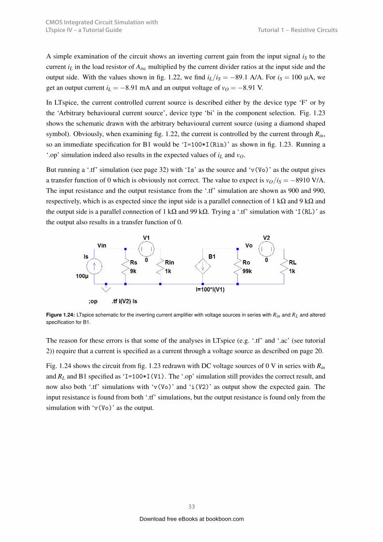
Figure 1.24: LTspice schematic for the inverting current amplifier with voltage sources in series with Rin and RL and alteredspecification for B1.
The reason for these errors is that some of the analyses in LTspice (e.g. ‘.tf’ and ‘.ac’ (see tutorial2)) require that a current is specified as a current through a voltage source as described on page 20.
Fig. 1.24 shows the circuit from fig. 1.23 redrawn with DC voltage sources of 0 V in series with Rin
and RL and B1 specified as ‘I=100*I(V1). The ‘.op’ simulation still provides the correct result, andnow also both ‘.tf’ simulations with ‘v(Vo)’ and ‘i(V2)’ as output show the expected gain. Theinput resistance is found from both ‘.tf’ simulations, but the output resistance is found only from thesimulation with ‘v(Vo)’ as the output.
Now, let us connect a feedback resistor R f of 15 kΩ between output and input as shown in fig. 1.25,
33
Download free eBooks at bookboon.com

CMOS Integrated Circuit Simulation with LTspice IV – a Tutorial Guide
34
Tutorial 1 – Resistive Circuits
Figure 1.25: LTspice schematic for the inverting current amplifier with a feedback resistor R f .
Now, let us connect a feedback resistor R f of 15 kΩ between output and input as shown in fig. 1.25,shunt - shunt feedback (Sedra & Smith 2011). With this feedback resistor, the amplifier is turned intoa transresistance amplifier. With a very large current gain Aisc, we would expect a transresistanceequal to −R f and small values of input and output resistance. The ‘.tf’ simulation with vO as theoutput shows a gain (transresistance) of −12.6 kΩ, an input resistance of 136 Ω and an outputresistance of 149 Ω (including Rs and RL). Increasing Aisc to 1000, we find a gain very close to -15kΩ and input and output resistances in the range of 1 to 2 Ω.
Download free eBooks at bookboon.com
Click on the ad to read moreClick on the ad to read moreClick on the ad to read moreClick on the ad to read moreClick on the ad to read moreClick on the ad to read moreClick on the ad to read moreClick on the ad to read moreClick on the ad to read moreClick on the ad to read moreClick on the ad to read more
American online LIGS University
enroll by September 30th, 2014 and
save up to 16% on the tuition!
pay in 10 installments / 2 years
Interactive Online education visit www.ligsuniversity.com to
find out more!
is currently enrolling in theInteractive Online BBA, MBA, MSc,
DBA and PhD programs:
Note: LIGS University is not accredited by any nationally recognized accrediting agency listed by the US Secretary of Education. More info here.
CMOS Integrated Circuit Simulation with LTspice IV – a Tutorial Guide
35
Tutorial 1 – Resistive Circuits
CMOS Integrated Circuit Simulation with LTspice IV Tutorial 1
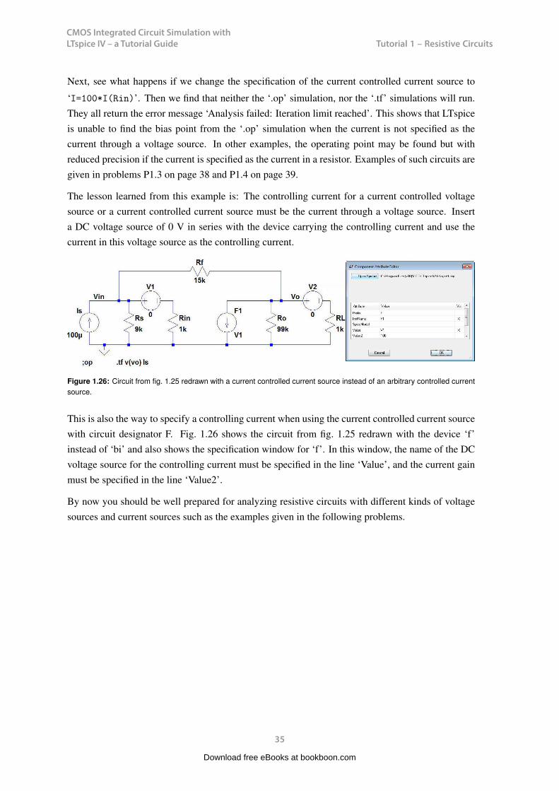
‘I=100*I(Rin)’. Then we find that neither the ‘.op’ simulation, nor the ‘.tf’ simulations will run.They all return the error message ‘Analysis failed: Iteration limit reached’. This shows that LTspiceis unable to find the bias point from the ‘.op’ simulation when the current is not specified as thecurrent through a voltage source. In other examples, the operating point may be found but withreduced precision if the current is specified as the current in a resistor. Examples of such circuits aregiven in problems P1.3 on page 38 and P1.4 on page 39.
The lesson learned from this example is: The controlling current for a current controlled voltagesource or a current controlled current source must be the current through a voltage source. Inserta DC voltage source of 0 V in series with the device carrying the controlling current and use thecurrent in this voltage source as the controlling current.
Figure 1.26: Circuit from fig. 1.25 redrawn with a current controlled current source instead of an arbitrary controlled currentsource.
This is also the way to specify a controlling current when using the current controlled current sourcewith circuit designator F. Fig. 1.26 shows the circuit from fig. 1.25 redrawn with the device ‘f’instead of ‘bi’ and also shows the specification window for ‘f’. In this window, the name of the DCvoltage source for the controlling current must be specified in the line ‘Value’, and the current gainmust be specified in the line ‘Value2’.
By now you should be well prepared for analyzing resistive circuits with different kinds of voltagesources and current sources such as the examples given in the following problems.
35
CMOS Integrated Circuit Simulation with LTspice IV Tutorial 1
Figure 1.25: LTspice schematic for the inverting current amplifier with a feedback resistor R f .
shunt - shunt feedback (Sedra & Smith 2011). With this feedback resistor, the amplifier is turned intoa transresistance amplifier. With a very large current gain Aisc, we would expect a transresistanceequal to −R f and small values of input and output resistance. The ‘.tf’ simulation with vO as theoutput shows a gain (transresistance) of −12.6 kΩ, an input resistance of 136 Ω and an outputresistance of 149 Ω (including Rs and RL). Increasing Aisc to 1000, we find a gain very close to -15kΩ and input and output resistances in the range of 1 to 2 Ω.
Next, see what happens if we change the specification of the current controlled current source to
34
Download free eBooks at bookboon.com
CMOS Integrated Circuit Simulation with LTspice IV – a Tutorial Guide
36
Tutorial 1 – Resistive CircuitsCMOS Integrated Circuit Simulation with LTspice IV Tutorial 1
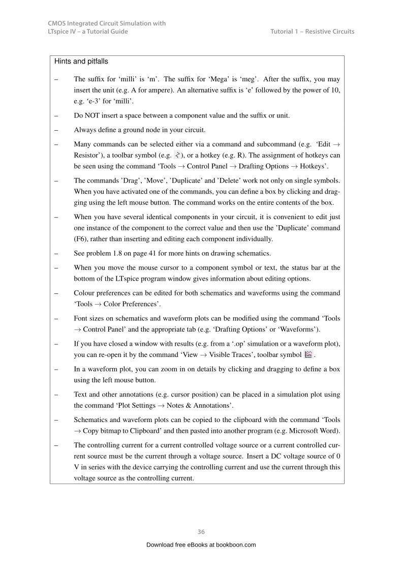
Hints and pitfalls
– The suffix for ‘milli’ is ‘m’. The suffix for ‘Mega’ is ‘meg’. After the suffix, you mayinsert the unit (e.g. A for ampere). An alternative suffix is ‘e’ followed by the power of 10,e.g. ‘e-3’ for ‘milli’.
– Do NOT insert a space between a component value and the suffix or unit.
– Always define a ground node in your circuit.
– Many commands can be selected either via a command and subcommand (e.g. ‘Edit →Resistor’), a toolbar symbol (e.g. ), or a hotkey (e.g. R). The assignment of hotkeys canbe seen using the command ‘Tools → Control Panel → Drafting Options → Hotkeys’.
– The commands ’Drag’, ’Move’, ’Duplicate’ and ’Delete’ work not only on single symbols.When you have activated one of the commands, you can define a box by clicking and drag-ging using the left mouse button. The command works on the entire contents of the box.
– When you have several identical components in your circuit, it is convenient to edit justone instance of the component to the correct value and then use the ’Duplicate’ command(F6), rather than inserting and editing each component individually.
– See problem 1.8 on page 41 for more hints on drawing schematics.
– When you move the mouse cursor to a component symbol or text, the status bar at thebottom of the LTspice program window gives information about editing options.
– Colour preferences can be edited for both schematics and waveforms using the command‘Tools → Color Preferences’.
– Font sizes on schematics and waveform plots can be modified using the command ‘Tools→ Control Panel’ and the appropriate tab (e.g. ‘Drafting Options’ or ‘Waveforms’).
– If you have closed a window with results (e.g. from a ‘.op’ simulation or a waveform plot),you can re-open it by the command ‘View → Visible Traces’, toolbar symbol .
– In a waveform plot, you can zoom in on details by clicking and dragging to define a boxusing the left mouse button.
– Text and other annotations (e.g. cursor position) can be placed in a simulation plot usingthe command ‘Plot Settings → Notes & Annotations’.
– Schematics and waveform plots can be copied to the clipboard with the command ‘Tools→ Copy bitmap to Clipboard’ and then pasted into another program (e.g. Microsoft Word).
– The controlling current for a current controlled voltage source or a current controlled cur-rent source must be the current through a voltage source. Insert a DC voltage source of 0V in series with the device carrying the controlling current and use the current through thisvoltage source as the controlling current.
36
Download free eBooks at bookboon.com

CMOS Integrated Circuit Simulation with LTspice IV – a Tutorial Guide
37
Tutorial 1 – Resistive CircuitsCMOS Integrated Circuit Simulation with LTspice IV Tutorial 1
References
Hambley, AR. 2014, Electrical Engineering, Principles and Applications, Sixth Edition, PearsonEducation Ltd., Harlow, UK.
Sedra, AS. & Smith, KC. 2011, Microelectronic Circuits, International Sixth Edition, Oxford Uni-versity Press, New York, USA.
Tuinenga, PW. 1995, Spice: A Guide to Circuit Simulation and Analysis Using PSpice, Third Edi-tion, Prentice Hall, Upper Saddle River, USA.
Vladimirescu, A. 1994, The SPICE book, First Edition, John Wiley & Sons, Hoboken, USA.
37
Download free eBooks at bookboon.com
Click on the ad to read moreClick on the ad to read moreClick on the ad to read moreClick on the ad to read moreClick on the ad to read moreClick on the ad to read moreClick on the ad to read moreClick on the ad to read moreClick on the ad to read moreClick on the ad to read moreClick on the ad to read moreClick on the ad to read more
.
CMOS Integrated Circuit Simulation with LTspice IV – a Tutorial Guide
38
Tutorial 1 – Resistive CircuitsCMOS Integrated Circuit Simulation with LTspice IV Tutorial 1
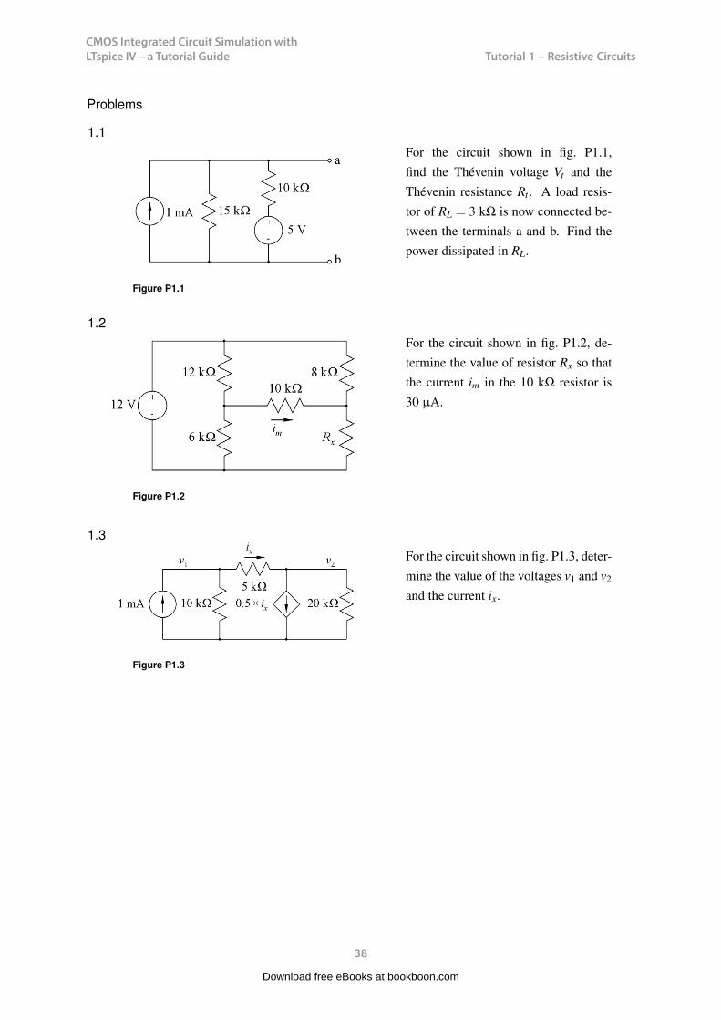
Problems
1.1
Figure P1.1
For the circuit shown in fig. P1.1,find the Thévenin voltage Vt and theThévenin resistance Rt . A load resis-tor of RL = 3 kΩ is now connected be-tween the terminals a and b. Find thepower dissipated in RL.
1.2
Figure P1.2
For the circuit shown in fig. P1.2, de-termine the value of resistor Rx so thatthe current im in the 10 kΩ resistor is30 µA.
1.3
Figure P1.3
For the circuit shown in fig. P1.3, deter-mine the value of the voltages v1 and v2
and the current ix.
38
Download free eBooks at bookboon.com

CMOS Integrated Circuit Simulation with LTspice IV – a Tutorial Guide
39
Tutorial 1 – Resistive CircuitsCMOS Integrated Circuit Simulation with LTspice IV Tutorial 1
1.4
Figure P1.4
For the circuit shown in fig. P1.4, findthe equivalent resistance looking intoterminals a – b.
1.5
Figure P1.5
For the circuit shown in fig. P1.5, findthe value of the gain Avoc which givesan output power in RL of 1 W whenthe signal voltage vs is 50 mV. Withthis value of Avoc, plot the output powerversus the input voltage for vs in therange from 0 mV to 100 mV.
39
Download free eBooks at bookboon.com
Click on the ad to read moreClick on the ad to read moreClick on the ad to read moreClick on the ad to read moreClick on the ad to read moreClick on the ad to read moreClick on the ad to read moreClick on the ad to read moreClick on the ad to read moreClick on the ad to read moreClick on the ad to read moreClick on the ad to read moreClick on the ad to read more
www.mastersopenday.nl
Visit us and find out why we are the best!Master’s Open Day: 22 February 2014
Join the best atthe Maastricht UniversitySchool of Business andEconomics!
Top master’s programmes• 33rdplaceFinancialTimesworldwideranking:MScInternationalBusiness
• 1stplace:MScInternationalBusiness• 1stplace:MScFinancialEconomics• 2ndplace:MScManagementofLearning• 2ndplace:MScEconomics• 2ndplace:MScEconometricsandOperationsResearch• 2ndplace:MScGlobalSupplyChainManagementandChange
Sources: Keuzegids Master ranking 2013; Elsevier ‘Beste Studies’ ranking 2012; Financial Times Global Masters in Management ranking 2012
MaastrichtUniversity is
the best specialistuniversity in the
Netherlands(Elsevier)
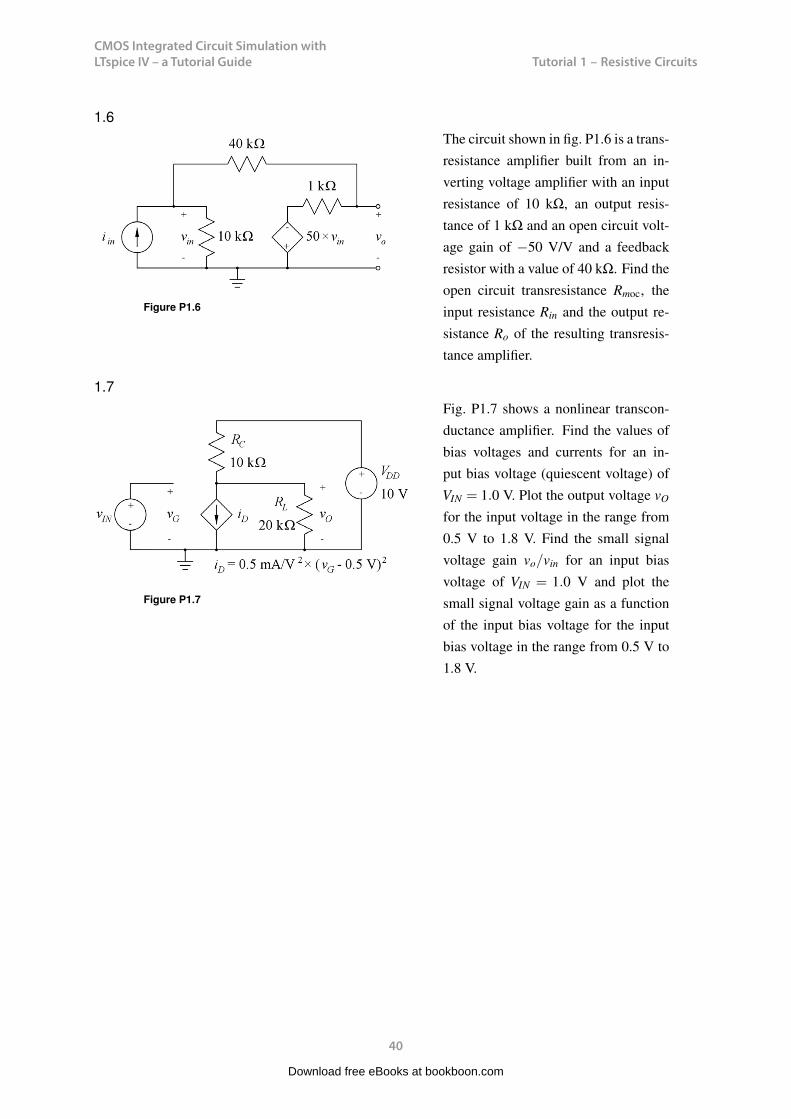
CMOS Integrated Circuit Simulation with LTspice IV – a Tutorial Guide
40
Tutorial 1 – Resistive CircuitsCMOS Integrated Circuit Simulation with LTspice IV Tutorial 1
1.6
Figure P1.6
The circuit shown in fig. P1.6 is a trans-resistance amplifier built from an in-verting voltage amplifier with an inputresistance of 10 kΩ, an output resis-tance of 1 kΩ and an open circuit volt-age gain of −50 V/V and a feedbackresistor with a value of 40 kΩ. Find theopen circuit transresistance Rmoc, theinput resistance Rin and the output re-sistance Ro of the resulting transresis-tance amplifier.
1.7
Figure P1.7
Fig. P1.7 shows a nonlinear transcon-ductance amplifier. Find the values ofbias voltages and currents for an in-put bias voltage (quiescent voltage) ofVIN = 1.0 V. Plot the output voltage vO
for the input voltage in the range from0.5 V to 1.8 V. Find the small signalvoltage gain vo/vin for an input biasvoltage of VIN = 1.0 V and plot thesmall signal voltage gain as a functionof the input bias voltage for the inputbias voltage in the range from 0.5 V to1.8 V.
40
Download free eBooks at bookboon.com
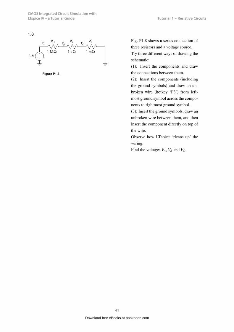
CMOS Integrated Circuit Simulation with LTspice IV – a Tutorial Guide
41
Tutorial 1 – Resistive CircuitsCMOS Integrated Circuit Simulation with LTspice IV Tutorial 1
1.8
Figure P1.8
Fig. P1.8 shows a series connection ofthree resistors and a voltage source.Try three different ways of drawing theschematic:(1): Insert the components and drawthe connections between them.(2): Insert the components (includingthe ground symbols) and draw an un-broken wire (hotkey ‘F3’) from left-most ground symbol across the compo-nents to rightmost ground symbol.(3): Insert the ground symbols, draw anunbroken wire between them, and theninsert the component directly on top ofthe wire.Observe how LTspice ‘cleans up’ thewiring.Find the voltages VA, VB and VC.
41
Download free eBooks at bookboon.com

CMOS Integrated Circuit Simulation with LTspice IV – a Tutorial Guide
42
Tutorial 1 – Resistive CircuitsCMOS Integrated Circuit Simulation with LTspice IV Tutorial 1
Answers
1.1: Vt = 9 V; Rt = 6 kΩ; PRL = 3 mW.
1.2: Rx = 3.31 kΩ.
1.3: v1 = 6 V; v2 = 4 V; ix = 0.4 mA.
1.4: Rab = 3.387 kΩ.
1.5: Avoc = 70 V/V.
1.6: Rmoc =−36.28 kΩ; Rin = 744 Ω; Ro = 90.7 Ω.
1.7: Bias point: ID = 0.125 mA; IC = 0.417 mA; IL = 0.292 mA; VO = 5.83 V.Small signal voltage gain with VIN = 1.0 V: vo/vin =−3.33 V/V.
1.8: VA = 3.0000 V; VB = 2.997 mV; VC = 2.997 nV.
42
Download free eBooks at bookboon.com
Click on the ad to read moreClick on the ad to read moreClick on the ad to read moreClick on the ad to read moreClick on the ad to read moreClick on the ad to read moreClick on the ad to read moreClick on the ad to read moreClick on the ad to read moreClick on the ad to read moreClick on the ad to read moreClick on the ad to read moreClick on the ad to read moreClick on the ad to read more
- ©
Pho
tono
nsto
p
> Apply now
redefine your future
AxA globAl grAduAte progrAm 2015
axa_ad_grad_prog_170x115.indd 1 19/12/13 16:36
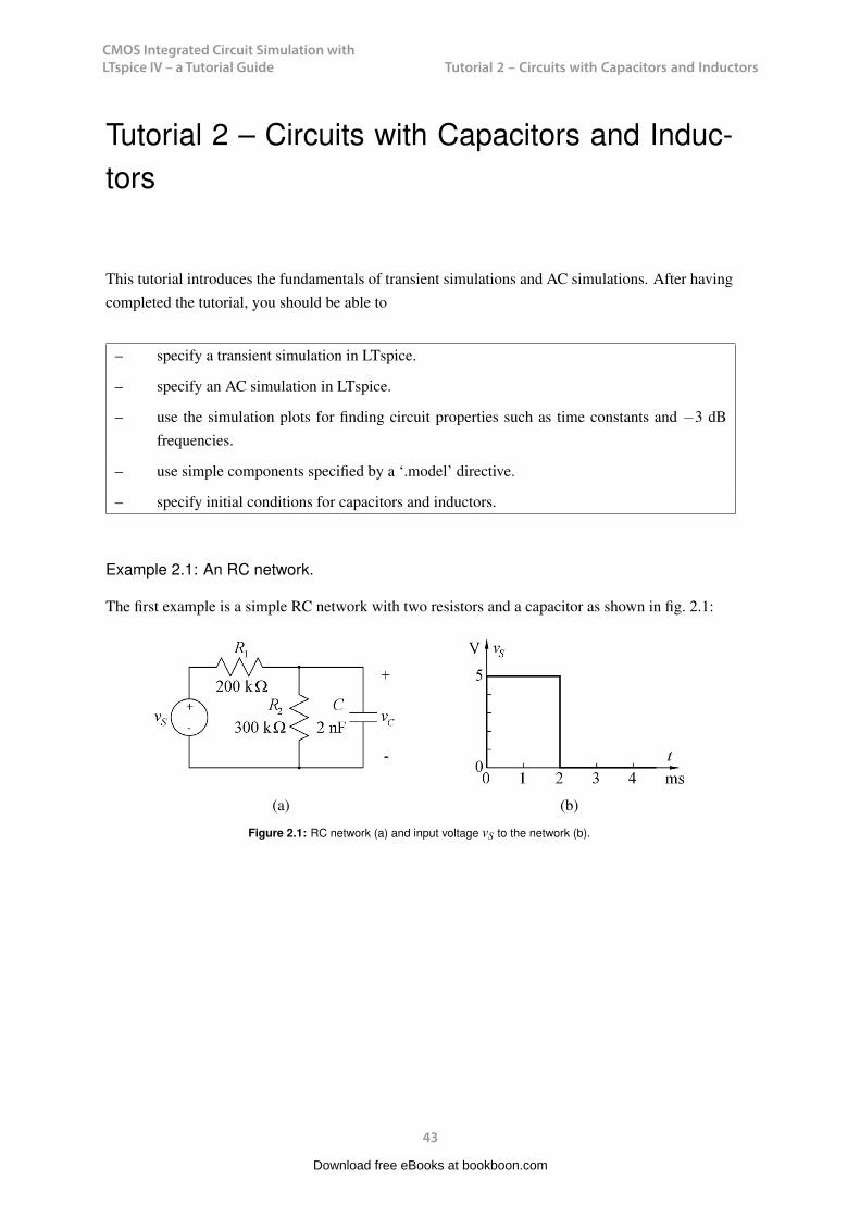
CMOS Integrated Circuit Simulation with LTspice IV – a Tutorial Guide
43
Tutorial 2 – Circuits with Capacitors and Inductors
CMOS Integrated Circuit Simulation with LTspice IV Tutorial 2
Tutorial 2 – Circuits with Capacitors and Induc-tors
This tutorial introduces the fundamentals of transient simulations and AC simulations. After havingcompleted the tutorial, you should be able to
– specify a transient simulation in LTspice.
– specify an AC simulation in LTspice.
– use the simulation plots for finding circuit properties such as time constants and −3 dBfrequencies.
– use simple components specified by a ‘.model’ directive.
– specify initial conditions for capacitors and inductors.
Example 2.1: An RC network.
The first example is a simple RC network with two resistors and a capacitor as shown in fig. 2.1:
(a) (b)
Figure 2.1: RC network (a) and input voltage vS to the network (b).
43
Download free eBooks at bookboon.com

CMOS Integrated Circuit Simulation with LTspice IV – a Tutorial Guide
44
Tutorial 2 – Circuits with Capacitors and InductorsCMOS Integrated Circuit Simulation with LTspice IV Tutorial 2
Transient response: Let us assume that the voltage source vS is a time varying voltage as shownin fig. 2.1(b). The voltage jumps from 0 V to a value of 5 V at time t = 0 and returns to 0 V atthe time t = 2 ms. This will cause the capacitor to charge and discharge. For a simulation of thecharging and discharging, we will run a transient simulation and specify the voltage source vS as atime varying voltage. The circuit is drawn in LTspice using the selection of editing commands as intutorial 1. The capacitor is available both as a command, ‘Edit → Capacitor’, as a toolbar symbol
, and as a hotkey ‘C’.
When specifying the voltage source vS, you point to the centre of the symbol. This turns the cur-sor into a hand . A right mouse click opens a window for specifying the voltage source. Inthis window, left click on ‘Advanced’. This opens a dialogue box where you may select time vary-ing functions, e.g. PWL, piecewise linear. A series of boxes for entering times and values willappear. Notice that the voltage cannot be changed abruptly, so the vertical edges from fig. 2.1(b)have to have a certain slope. Corresponding to the timing in fig. 2.1(b), you may enter time1=0s,value1=0V, time2=0.1us, value2=5V, time3=2ms, value3=5V, time4=2.0001ms, value4=0V. In thisway, the voltage changes from 0 V to 5 V in 0.1 µs. An alternative to specifying time4 as 2.0001msis to specify time4=2ms+0.1us. Remember to include the curly brackets ‘’, otherwise youwill receive an error message and the simulation will not run. Also note that you may include theunits (’s’ for seconds and ‘V’ for volts). This makes it easier to read the specification shown on
44
Download free eBooks at bookboon.com
Click on the ad to read moreClick on the ad to read moreClick on the ad to read moreClick on the ad to read moreClick on the ad to read moreClick on the ad to read moreClick on the ad to read moreClick on the ad to read moreClick on the ad to read moreClick on the ad to read moreClick on the ad to read moreClick on the ad to read moreClick on the ad to read moreClick on the ad to read moreClick on the ad to read more
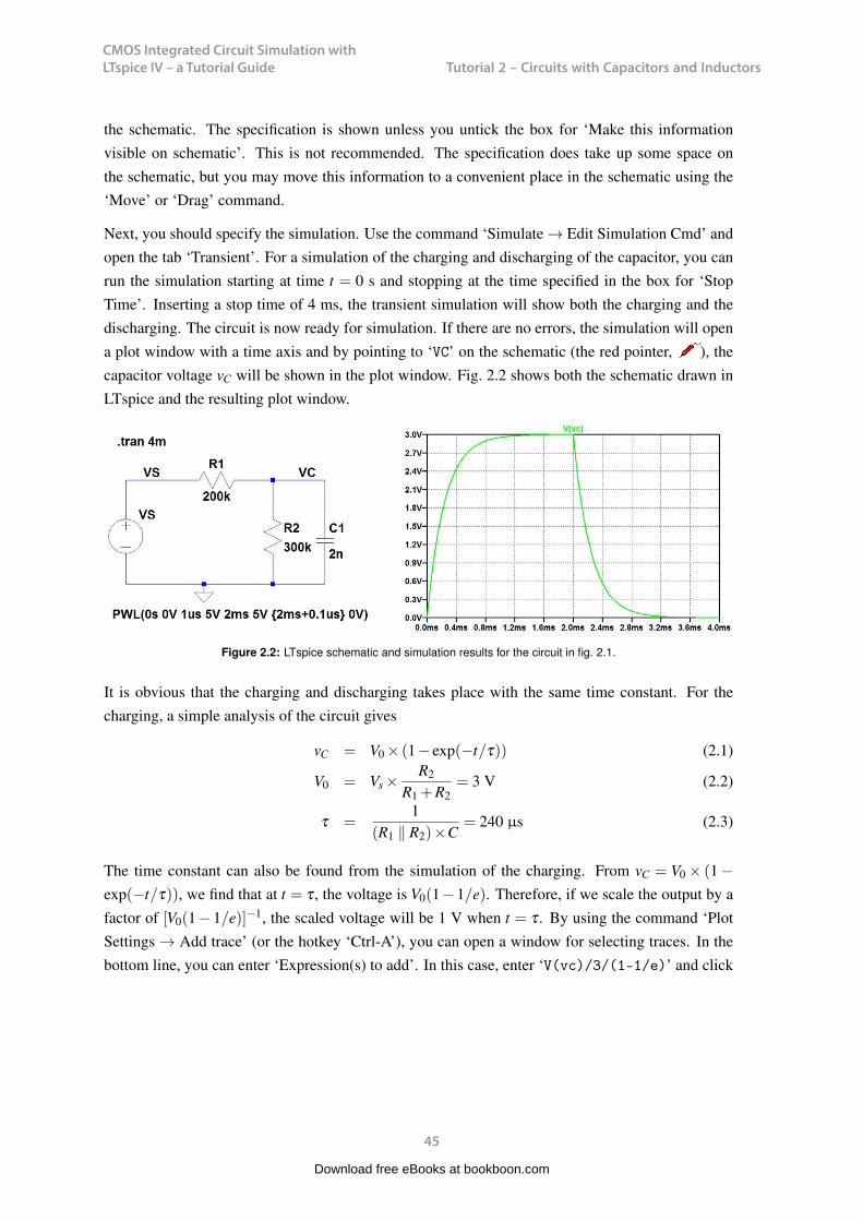
CMOS Integrated Circuit Simulation with LTspice IV – a Tutorial Guide
45
Tutorial 2 – Circuits with Capacitors and InductorsCMOS Integrated Circuit Simulation with LTspice IV Tutorial 2
the schematic. The specification is shown unless you untick the box for ‘Make this informationvisible on schematic’. This is not recommended. The specification does take up some space onthe schematic, but you may move this information to a convenient place in the schematic using the‘Move’ or ‘Drag’ command.
Next, you should specify the simulation. Use the command ‘Simulate → Edit Simulation Cmd’ andopen the tab ‘Transient’. For a simulation of the charging and discharging of the capacitor, you canrun the simulation starting at time t = 0 s and stopping at the time specified in the box for ‘StopTime’. Inserting a stop time of 4 ms, the transient simulation will show both the charging and thedischarging. The circuit is now ready for simulation. If there are no errors, the simulation will opena plot window with a time axis and by pointing to ‘VC’ on the schematic (the red pointer, ), thecapacitor voltage vC will be shown in the plot window. Fig. 2.2 shows both the schematic drawn inLTspice and the resulting plot window.
Figure 2.2: LTspice schematic and simulation results for the circuit in fig. 2.1.
It is obvious that the charging and discharging takes place with the same time constant. For thecharging, a simple analysis of the circuit gives
vC = V0 × (1− exp(−t/τ)) (2.1)
V0 = Vs ×R2
R1 +R2= 3 V (2.2)
τ =1
(R1 ‖ R2)×C= 240 µs (2.3)
The time constant can also be found from the simulation of the charging. From vC = V0 × (1−exp(−t/τ)), we find that at t = τ , the voltage is V0(1−1/e). Therefore, if we scale the output by afactor of [V0(1− 1/e)]−1, the scaled voltage will be 1 V when t = τ . By using the command ‘PlotSettings → Add trace’ (or the hotkey ‘Ctrl-A’), you can open a window for selecting traces. In thebottom line, you can enter ‘Expression(s) to add’. In this case, enter ‘V(vc)/3/(1-1/e)’ and click
45
Download free eBooks at bookboon.com
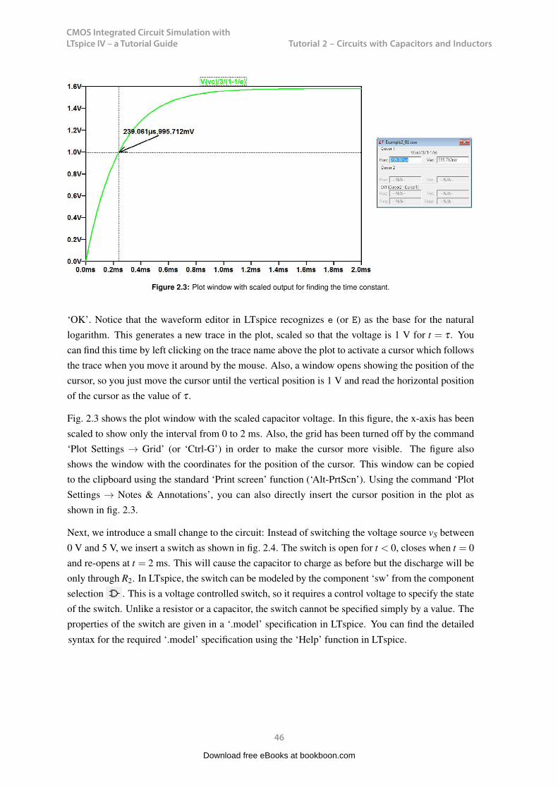
CMOS Integrated Circuit Simulation with LTspice IV – a Tutorial Guide
46
Tutorial 2 – Circuits with Capacitors and InductorsCMOS Integrated Circuit Simulation with LTspice IV Tutorial 2
Figure 2.3: Plot window with scaled output for finding the time constant.
‘OK’. Notice that the waveform editor in LTspice recognizes e (or E) as the base for the naturallogarithm. This generates a new trace in the plot, scaled so that the voltage is 1 V for t = τ . Youcan find this time by left clicking on the trace name above the plot to activate a cursor which followsthe trace when you move it around by the mouse. Also, a window opens showing the position of thecursor, so you just move the cursor until the vertical position is 1 V and read the horizontal positionof the cursor as the value of τ .
Fig. 2.3 shows the plot window with the scaled capacitor voltage. In this figure, the x-axis has beenscaled to show only the interval from 0 to 2 ms. Also, the grid has been turned off by the command‘Plot Settings → Grid’ (or ‘Ctrl-G’) in order to make the cursor more visible. The figure alsoshows the window with the coordinates for the position of the cursor. This window can be copiedto the clipboard using the standard ‘Print screen’ function (‘Alt-PrtScn’). Using the command ‘PlotSettings → Notes & Annotations’, you can also directly insert the cursor position in the plot asshown in fig. 2.3.
Next, we introduce a small change to the circuit: Instead of switching the voltage source vS between0 V and 5 V, we insert a switch as shown in fig. 2.4. The switch is open for t < 0, closes when t = 0and re-opens at t = 2 ms. This will cause the capacitor to charge as before but the discharge will beonly through R2. In LTspice, the switch can be modeled by the component ‘sw’ from the componentselection . This is a voltage controlled switch, so it requires a control voltage to specify the stateof the switch. Unlike a resistor or a capacitor, the switch cannot be specified simply by a value. Theproperties of the switch are given in a ‘.model’ specification in LTspice. You can find the detailed
46
CMOS Integrated Circuit Simulation with LTspice IV Tutorial 2
Figure 2.4: The RC network from fig. 2.1 with a switch between the voltage source and the resistor R1.
Figure 2.5: LTspice schematic and simulation results for the circuit in fig. 2.4.
syntax for the required ‘.model’ specification using the ‘Help’ function in LTspice.
When you insert the switch in the schematic, it appears with a reference to a default switch modelSW. You may use the default model without inserting a ‘.model’ specification. If you wish to changesome parameters of the switch, you must include a ‘.model’ specification and it is a good idea to useanother name for the model, rather than the default SW.
Fig. 2.5 shows the LTspice schematic including a ‘.model’ specification which is inserted using thecommand ‘Edit → SPICE Directive’ (or the toolbar symbol ). The ‘.model’ specification firstspecifies that the device to be modeled is the device using the model name ‘VSW’ in the schematic.Next, the model used is the standard LTspice model ‘SW’ which is specified by some parametersgiven in the brackets. In this case, only the threshold of the switch is changed from the default valueof 0 V, so that we can use the signal specification from fig. 2.2 for the control signal to the switch.Also note that the model is named VSW to distinguish it from the default name.
The ‘.model’ specification is shown on the schematic with a smaller font size than otherwise used inthe schematic. The font size is selected when inserting the specification (or when editing the spec-ification). You can also make a ‘global’ change of the font size on schematics using the command‘Tools → Control Panel’ and the tab ‘Drafting Options’.
47
Download free eBooks at bookboon.com
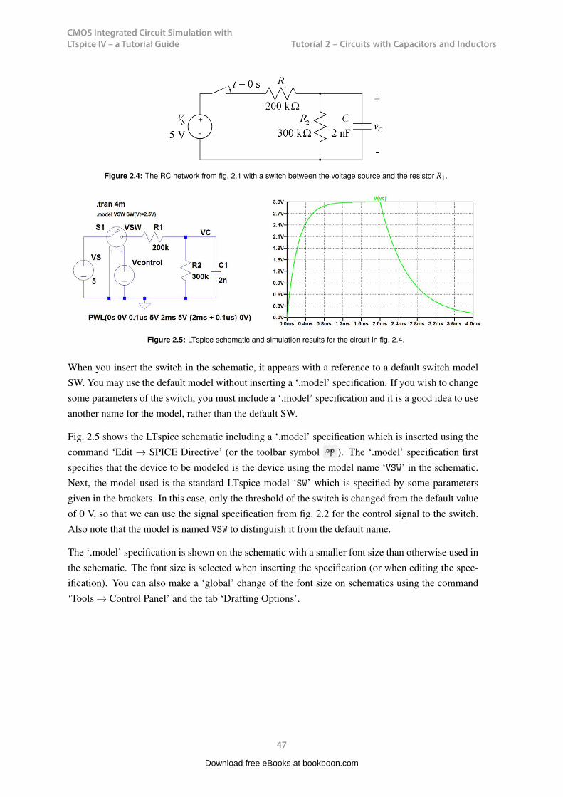
CMOS Integrated Circuit Simulation with LTspice IV – a Tutorial Guide
47
Tutorial 2 – Circuits with Capacitors and InductorsCMOS Integrated Circuit Simulation with LTspice IV Tutorial 2
Figure 2.4: The RC network from fig. 2.1 with a switch between the voltage source and the resistor R1.
Figure 2.5: LTspice schematic and simulation results for the circuit in fig. 2.4.
syntax for the required ‘.model’ specification using the ‘Help’ function in LTspice.
When you insert the switch in the schematic, it appears with a reference to a default switch modelSW. You may use the default model without inserting a ‘.model’ specification. If you wish to changesome parameters of the switch, you must include a ‘.model’ specification and it is a good idea to useanother name for the model, rather than the default SW.
Fig. 2.5 shows the LTspice schematic including a ‘.model’ specification which is inserted using thecommand ‘Edit → SPICE Directive’ (or the toolbar symbol ). The ‘.model’ specification firstspecifies that the device to be modeled is the device using the model name ‘VSW’ in the schematic.Next, the model used is the standard LTspice model ‘SW’ which is specified by some parametersgiven in the brackets. In this case, only the threshold of the switch is changed from the default valueof 0 V, so that we can use the signal specification from fig. 2.2 for the control signal to the switch.Also note that the model is named VSW to distinguish it from the default name.
The ‘.model’ specification is shown on the schematic with a smaller font size than otherwise used inthe schematic. The font size is selected when inserting the specification (or when editing the spec-ification). You can also make a ‘global’ change of the font size on schematics using the command‘Tools → Control Panel’ and the tab ‘Drafting Options’.
47
CMOS Integrated Circuit Simulation with LTspice IV Tutorial 2
Figure 2.4: The RC network from fig. 2.1 with a switch between the voltage source and the resistor R1.
Figure 2.5: LTspice schematic and simulation results for the circuit in fig. 2.4.
syntax for the required ‘.model’ specification using the ‘Help’ function in LTspice.
When you insert the switch in the schematic, it appears with a reference to a default switch modelSW. You may use the default model without inserting a ‘.model’ specification. If you wish to changesome parameters of the switch, you must include a ‘.model’ specification and it is a good idea to useanother name for the model, rather than the default SW.
Fig. 2.5 shows the LTspice schematic including a ‘.model’ specification which is inserted using thecommand ‘Edit → SPICE Directive’ (or the toolbar symbol ). The ‘.model’ specification firstspecifies that the device to be modeled is the device using the model name ‘VSW’ in the schematic.Next, the model used is the standard LTspice model ‘SW’ which is specified by some parametersgiven in the brackets. In this case, only the threshold of the switch is changed from the default valueof 0 V, so that we can use the signal specification from fig. 2.2 for the control signal to the switch.Also note that the model is named VSW to distinguish it from the default name.
The ‘.model’ specification is shown on the schematic with a smaller font size than otherwise used inthe schematic. The font size is selected when inserting the specification (or when editing the spec-ification). You can also make a ‘global’ change of the font size on schematics using the command‘Tools → Control Panel’ and the tab ‘Drafting Options’.
47
Download free eBooks at bookboon.com

CMOS Integrated Circuit Simulation with LTspice IV – a Tutorial Guide
48
Tutorial 2 – Circuits with Capacitors and InductorsCMOS Integrated Circuit Simulation with LTspice IV Tutorial 2
In this schematic, the voltage VS is specified as a dc voltage and the time varying signal to controlthe switch is the voltage source ‘Vcontrol’ which is specified as a piecewise linear voltage sourcewith the same specification as the input voltage for the circuit in fig. 2.2. Also shown in fig. 2.5 isthe simulation result for vC, compare fig. 2.2.
It is clear from the simulation that the time constant for discharging the capacitor is now larger thanthe time constant for charging. The time constant for charging is the same as before, i.e. 240 µs.The time constant for discharging is now τ = R2 ×C = 600 µs. By scaling the voltage vC in thesame way as in fig. 2.3, you can use the cursors in the plot window to find the time constants. Notethat two cursors are available, so by placing one cursor at the start time for the discharge (2 ms) andthe other so that the vertical difference between the two cursors is 1 V, you can estimate the timeconstant to be the horizontal difference between the two cursors, see fig. 2.6.
AC response: The circuit shown in fig. 2.1 is a first-order lowpass filter with the transfer functionVc( jω)/Vs( jω) = G0/(1+ j(ω/ω 0)) where G0 = R2/(R1 +R2) = 0.6 (or −4.44 dB) is the lowfrequency gain and ω 0 = 1/τ = 1/((R1 ‖ R2)×C)) = 4.17× 10³ s−1 (or 663 Hz) is the −3 dBfrequency. This frequency response is normally shown in a Bode plot. In LTspice, the transferfunction is simulated using the ‘.ac’ simulation command. Use ‘Simulate → Edit Simulation Cmd’and select the tab ‘AC Analysis’. Here you can specify the type of sweep, start frequency, stop
48
Download free eBooks at bookboon.com
Click on the ad to read moreClick on the ad to read moreClick on the ad to read moreClick on the ad to read moreClick on the ad to read moreClick on the ad to read moreClick on the ad to read moreClick on the ad to read moreClick on the ad to read moreClick on the ad to read moreClick on the ad to read moreClick on the ad to read moreClick on the ad to read moreClick on the ad to read moreClick on the ad to read moreClick on the ad to read more
Get Help Now
Go to www.helpmyassignment.co.uk for more info
Need help with yourdissertation?Get in-depth feedback & advice from experts in your topic area. Find out what you can do to improvethe quality of your dissertation!
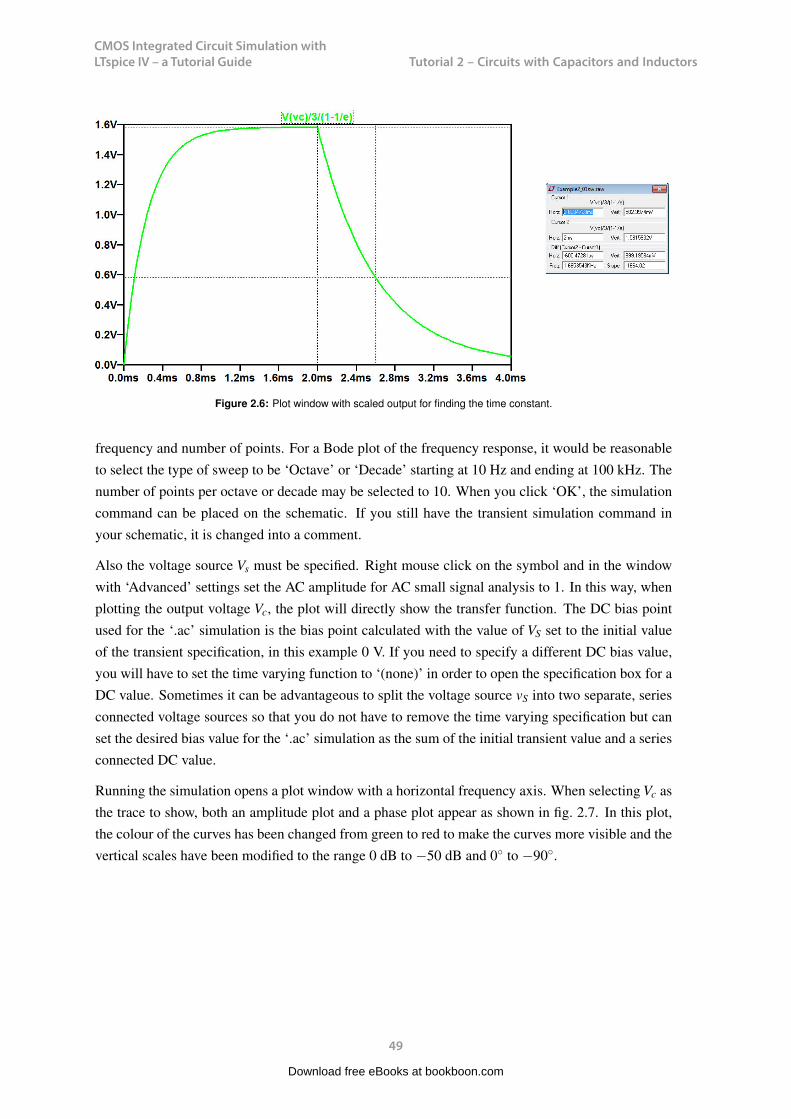
CMOS Integrated Circuit Simulation with LTspice IV – a Tutorial Guide
49
Tutorial 2 – Circuits with Capacitors and InductorsCMOS Integrated Circuit Simulation with LTspice IV Tutorial 2
Figure 2.6: Plot window with scaled output for finding the time constant.
frequency and number of points. For a Bode plot of the frequency response, it would be reasonableto select the type of sweep to be ‘Octave’ or ‘Decade’ starting at 10 Hz and ending at 100 kHz. Thenumber of points per octave or decade may be selected to 10. When you click ‘OK’, the simulationcommand can be placed on the schematic. If you still have the transient simulation command inyour schematic, it is changed into a comment.
Also the voltage source Vs must be specified. Right mouse click on the symbol and in the windowwith ‘Advanced’ settings set the AC amplitude for AC small signal analysis to 1. In this way, whenplotting the output voltage Vc, the plot will directly show the transfer function. The DC bias pointused for the ‘.ac’ simulation is the bias point calculated with the value of VS set to the initial valueof the transient specification, in this example 0 V. If you need to specify a different DC bias value,you will have to set the time varying function to ‘(none)’ in order to open the specification box for aDC value. Sometimes it can be advantageous to split the voltage source vS into two separate, seriesconnected voltage sources so that you do not have to remove the time varying specification but canset the desired bias value for the ‘.ac’ simulation as the sum of the initial transient value and a seriesconnected DC value.
Running the simulation opens a plot window with a horizontal frequency axis. When selecting Vc asthe trace to show, both an amplitude plot and a phase plot appear as shown in fig. 2.7. In this plot,the colour of the curves has been changed from green to red to make the curves more visible and thevertical scales have been modified to the range 0 dB to −50 dB and 0 to −90.
The −3 dB frequency is found using the cursors in a way similar to what was done for finding time
49
Download free eBooks at bookboon.com
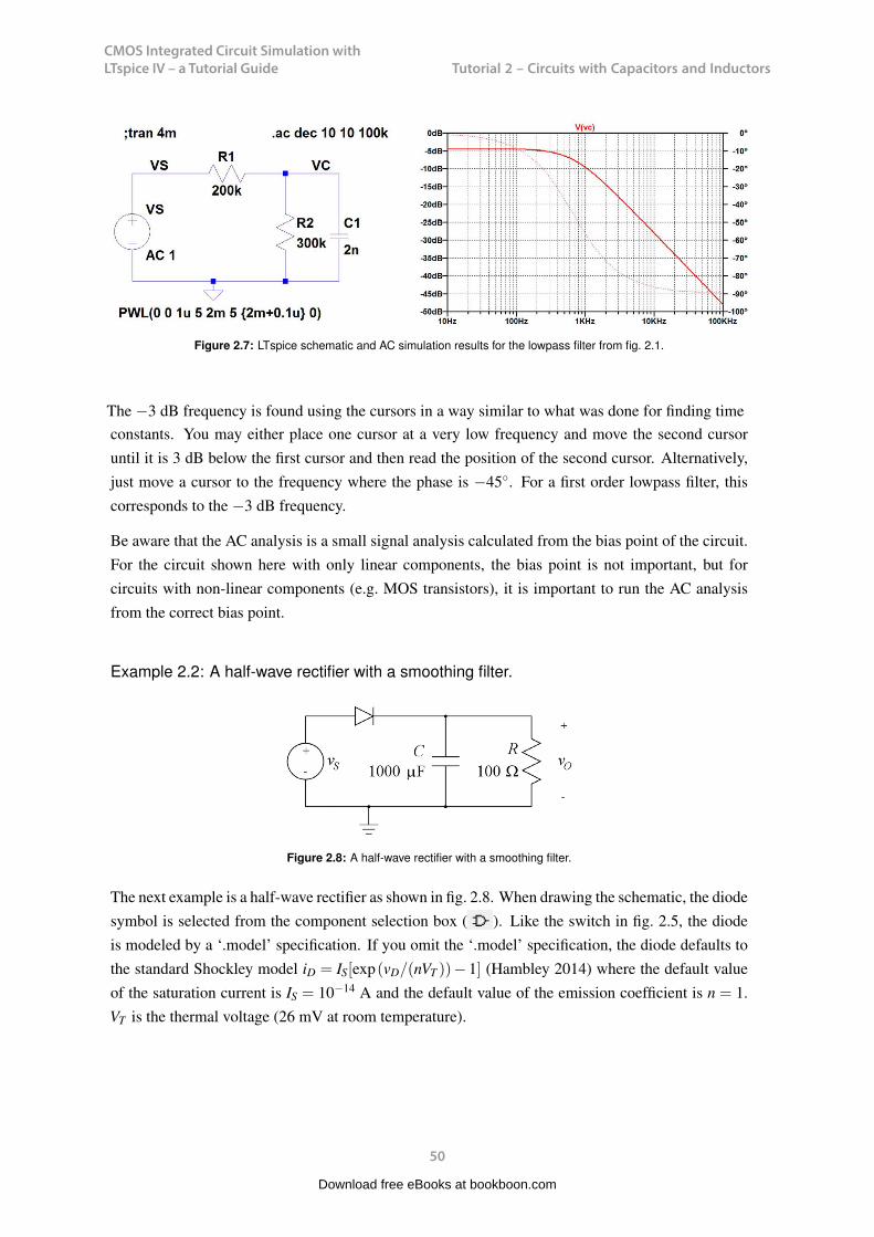
CMOS Integrated Circuit Simulation with LTspice IV – a Tutorial Guide
50
Tutorial 2 – Circuits with Capacitors and Inductors
CMOS Integrated Circuit Simulation with LTspice IV Tutorial 2
Figure 2.7: LTspice schematic and AC simulation results for the lowpass filter from fig. 2.1.
constants. You may either place one cursor at a very low frequency and move the second cursoruntil it is 3 dB below the first cursor and then read the position of the second cursor. Alternatively,just move a cursor to the frequency where the phase is −45. For a first order lowpass filter, thiscorresponds to the −3 dB frequency.
Be aware that the AC analysis is a small signal analysis calculated from the bias point of the circuit.For the circuit shown here with only linear components, the bias point is not important, but forcircuits with non-linear components (e.g. MOS transistors), it is important to run the AC analysisfrom the correct bias point.
Example 2.2: A half-wave rectifier with a smoothing filter.
Figure 2.8: A half-wave rectifier with a smoothing filter.
The next example is a half-wave rectifier as shown in fig. 2.8. When drawing the schematic, the diodesymbol is selected from the component selection box ( ). Like the switch in fig. 2.5, the diodeis modeled by a ‘.model’ specification. If you omit the ‘.model’ specification, the diode defaults tothe standard Shockley model iD = IS[exp(vD/(nVT ))− 1] (Hambley 2014) where the default valueof the saturation current is IS = 10−14 A and the default value of the emission coefficient is n = 1.VT is the thermal voltage (26 mV at room temperature).
50
CMOS Integrated Circuit Simulation with LTspice IV Tutorial 2
Figure 2.6: Plot window with scaled output for finding the time constant.
frequency and number of points. For a Bode plot of the frequency response, it would be reasonableto select the type of sweep to be ‘Octave’ or ‘Decade’ starting at 10 Hz and ending at 100 kHz. Thenumber of points per octave or decade may be selected to 10. When you click ‘OK’, the simulationcommand can be placed on the schematic. If you still have the transient simulation command inyour schematic, it is changed into a comment.
Also the voltage source Vs must be specified. Right mouse click on the symbol and in the windowwith ‘Advanced’ settings set the AC amplitude for AC small signal analysis to 1. In this way, whenplotting the output voltage Vc, the plot will directly show the transfer function. The DC bias pointused for the ‘.ac’ simulation is the bias point calculated with the value of VS set to the initial valueof the transient specification, in this example 0 V. If you need to specify a different DC bias value,you will have to set the time varying function to ‘(none)’ in order to open the specification box for aDC value. Sometimes it can be advantageous to split the voltage source vS into two separate, seriesconnected voltage sources so that you do not have to remove the time varying specification but canset the desired bias value for the ‘.ac’ simulation as the sum of the initial transient value and a seriesconnected DC value.
Running the simulation opens a plot window with a horizontal frequency axis. When selecting Vc asthe trace to show, both an amplitude plot and a phase plot appear as shown in fig. 2.7. In this plot,the colour of the curves has been changed from green to red to make the curves more visible and thevertical scales have been modified to the range 0 dB to −50 dB and 0 to −90.
The −3 dB frequency is found using the cursors in a way similar to what was done for finding time
49
CMOS Integrated Circuit Simulation with LTspice IV Tutorial 2
Figure 2.7: LTspice schematic and AC simulation results for the lowpass filter from fig. 2.1.
constants. You may either place one cursor at a very low frequency and move the second cursoruntil it is 3 dB below the first cursor and then read the position of the second cursor. Alternatively,just move a cursor to the frequency where the phase is −45. For a first order lowpass filter, thiscorresponds to the −3 dB frequency.
Be aware that the AC analysis is a small signal analysis calculated from the bias point of the circuit.For the circuit shown here with only linear components, the bias point is not important, but forcircuits with non-linear components (e.g. MOS transistors), it is important to run the AC analysisfrom the correct bias point.
Example 2.2: A half-wave rectifier with a smoothing filter.
Figure 2.8: A half-wave rectifier with a smoothing filter.
The next example is a half-wave rectifier as shown in fig. 2.8. When drawing the schematic, the diodesymbol is selected from the component selection box ( ). Like the switch in fig. 2.5, the diodeis modeled by a ‘.model’ specification. If you omit the ‘.model’ specification, the diode defaults tothe standard Shockley model iD = IS[exp(vD/(nVT ))− 1] (Hambley 2014) where the default valueof the saturation current is IS = 10−14 A and the default value of the emission coefficient is n = 1.VT is the thermal voltage (26 mV at room temperature).
50
Download free eBooks at bookboon.com

CMOS Integrated Circuit Simulation with LTspice IV – a Tutorial Guide
51
Tutorial 2 – Circuits with Capacitors and InductorsCMOS Integrated Circuit Simulation with LTspice IV Tutorial 2
Several models for different commercially available discrete type diodes are included with LTspiceand are contained in a library file. When selecting the diode, you point to the centre of the diodesymbol. This turns the cursor into a hand . A right mouse click opens a window as shown infig. 2.9. By clicking ‘Pick New Diode’, you open a window with a selection of standard componentdiodes. Selecting a diode and clicking ‘OK’ will insert the diode name on the schematic and insert alink to the appropriate ‘.model’ statement in the LTspice netlist file. If the selected diode is a Zenerdiode (or another type of diode), the symbol is also changed into the appropriate diode symbol.
Figure 2.9: Window for selecting diode model.
51
Download free eBooks at bookboon.com
Click on the ad to read moreClick on the ad to read moreClick on the ad to read moreClick on the ad to read moreClick on the ad to read moreClick on the ad to read moreClick on the ad to read moreClick on the ad to read moreClick on the ad to read moreClick on the ad to read moreClick on the ad to read moreClick on the ad to read moreClick on the ad to read moreClick on the ad to read moreClick on the ad to read moreClick on the ad to read moreClick on the ad to read more
By 2020, wind could provide one-tenth of our planet’s electricity needs. Already today, SKF’s innovative know-how is crucial to running a large proportion of the world’s wind turbines.
Up to 25 % of the generating costs relate to mainte-nance. These can be reduced dramatically thanks to our systems for on-line condition monitoring and automatic lubrication. We help make it more economical to create cleaner, cheaper energy out of thin air.
By sharing our experience, expertise, and creativity, industries can boost performance beyond expectations.
Therefore we need the best employees who can meet this challenge!
The Power of Knowledge Engineering
Brain power
Plug into The Power of Knowledge Engineering.
Visit us at www.skf.com/knowledge
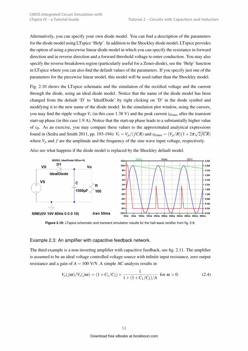
CMOS Integrated Circuit Simulation with LTspice IV – a Tutorial Guide
52
Tutorial 2 – Circuits with Capacitors and InductorsCMOS Integrated Circuit Simulation with LTspice IV Tutorial 2
Alternatively, you can specify your own diode model. You can find a description of the parametersfor the diode model using LTspice ‘Help’. In addition to the Shockley diode model, LTspice providesthe option of using a piecewise linear diode model in which you can specify the resistance in forwarddirection and in reverse direction and a forward threshold voltage to enter conduction. You may alsospecify the reverse breakdown region (particularly useful for a Zener-diode), see the ‘Help’ functionin LTspice where you can also find the default values of the parameters. If you specify just one of theparameters for the piecewise linear model, this model will be used rather than the Shockley model.
Fig. 2.10 shows the LTspice schematic and the simulation of the rectified voltage and the currentthrough the diode, using an ideal diode model. Notice that the name of the diode model has beenchanged from the default ‘D’ to ‘IdealDiode’ by right clicking on ‘D’ in the diode symbol andmodifying it to the new name of the diode model. In the simulation plot window, using the cursors,you may find the ripple voltage Vr (in this case 1.38 V) and the peak current iDmax after the transientstart-up phase (in this case 1.9 A). Notice that the start-up phase leads to a substantially higher valueof iD. As an exercise, you may compare these values to the approximated analytical expressionsfound in (Sedra and Smith 2011, pp. 193-194): Vr =Vp/( fCR) and iDmax = (Vp/R)(1+2π
√2 fCR)
where Vp and f are the amplitude and the frequency of the sine wave input voltage, respectively.
Also see what happens if the diode model is replaced by the Shockley default model.
Figure 2.10: LTspice schematic and transient simulation results for the half-wave rectifier from fig. 2.8.
Example 2.3: An amplifier with capacitive feedback network.
The third example is a non-inverting amplifier with capacitive feedback, see fig. 2.11. The amplifieris assumed to be an ideal voltage controlled voltage source with infinite input resistance, zero outputresistance and a gain of A = 100 V/V. A simple AC analysis results in
Vo( jω)/Vs( jω) = (1+C1/C2)×1
1+(1+C1/C2)/Afor ω > 0. (2.4)
52
Download free eBooks at bookboon.com
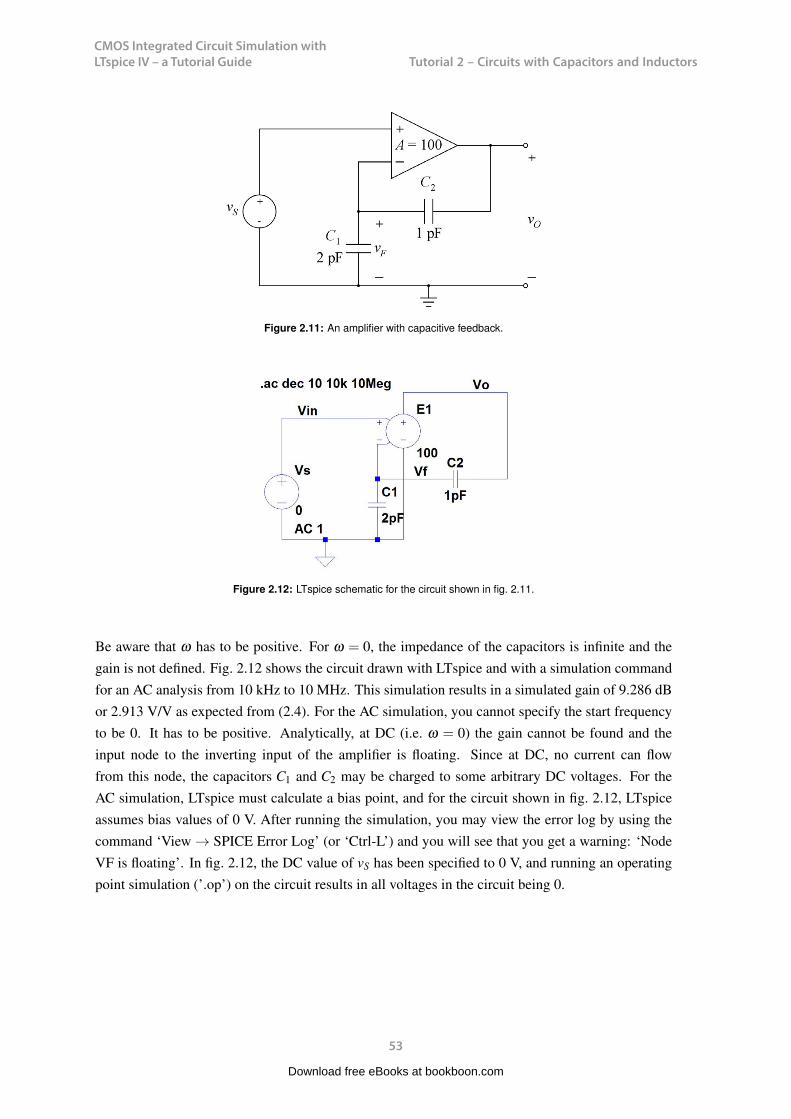
CMOS Integrated Circuit Simulation with LTspice IV – a Tutorial Guide
53
Tutorial 2 – Circuits with Capacitors and InductorsCMOS Integrated Circuit Simulation with LTspice IV Tutorial 2
Figure 2.11: An amplifier with capacitive feedback.
Figure 2.12: LTspice schematic for the circuit shown in fig. 2.11.
Be aware that ω has to be positive. For ω = 0, the impedance of the capacitors is infinite and thegain is not defined. Fig. 2.12 shows the circuit drawn with LTspice and with a simulation commandfor an AC analysis from 10 kHz to 10 MHz. This simulation results in a simulated gain of 9.286 dBor 2.913 V/V as expected from (2.4). For the AC simulation, you cannot specify the start frequencyto be 0. It has to be positive. Analytically, at DC (i.e. ω = 0) the gain cannot be found and theinput node to the inverting input of the amplifier is floating. Since at DC, no current can flowfrom this node, the capacitors C1 and C2 may be charged to some arbitrary DC voltages. For theAC simulation, LTspice must calculate a bias point, and for the circuit shown in fig. 2.12, LTspiceassumes bias values of 0 V. After running the simulation, you may view the error log by using thecommand ‘View → SPICE Error Log’ (or ‘Ctrl-L’) and you will see that you get a warning: ‘NodeVF is floating’. In fig. 2.12, the DC value of vS has been specified to 0 V, and running an operatingpoint simulation (’.op’) on the circuit results in all voltages in the circuit being 0.
53
Download free eBooks at bookboon.com

CMOS Integrated Circuit Simulation with LTspice IV – a Tutorial Guide
54
Tutorial 2 – Circuits with Capacitors and InductorsCMOS Integrated Circuit Simulation with LTspice IV Tutorial 2
If we change the DC value of vS to 1 V and run an operating point analysis, we find that the simulatedvalue of the output voltage is now 100 V, i.e. the amplifier just provides the open loop gain A. Thismay not be a realistic situation for a practical circuit, and again an examination of the error log givesa warning that node VF is floating. One possible solution to the problem of a floating node is toestablish a DC path to the node. For the circuit in fig. 2.12, a very large resistor (many gigaohms)may be connected in parallel with one of the capacitors. If connected in parallel with C1, the DCgain is the open loop gain of the amplifier, i.e. A = 100 V/V. If connected in parallel with C2, the DCgain of the amplifier is A/(1+A) = 0.9901 V/V.
For transient simulations, there is an alternative way of handling a floating node: the initial valueof the node voltage may be specified using a ‘.ic’ SPICE Directive. Assume for instance that thecircuit of fig. 2.11 has an initial value of the feedback voltage vF of 0.05 V. With an input voltageof vS = 0 V, this gives an initial value of the output voltage of vO =−A× vF =−5 V. Assume alsothat the input voltage vS is a periodic triangular voltage with period of 40 µs, an amplitude of 1 V,a mean value of 0 V, and a start value of 0 V at time t = 0. Fig. 2.13 shows the schematic withthis specification of vS, and the initial value of vF is set by the SPICE Directive (command ‘Edit→ SPICE Directive’) ‘.IC v(VF)=0.05V’. Also shown in fig. 2.13 is the result of the transientsimulation, showing the input voltage and the output voltage. It is evident that the gain of the circuitis about 3 V/V as expected and that the output voltage is offset by −5 V.
54
Download free eBooks at bookboon.com
Click on the ad to read moreClick on the ad to read moreClick on the ad to read moreClick on the ad to read moreClick on the ad to read moreClick on the ad to read moreClick on the ad to read moreClick on the ad to read moreClick on the ad to read moreClick on the ad to read moreClick on the ad to read moreClick on the ad to read moreClick on the ad to read moreClick on the ad to read moreClick on the ad to read moreClick on the ad to read moreClick on the ad to read moreClick on the ad to read more
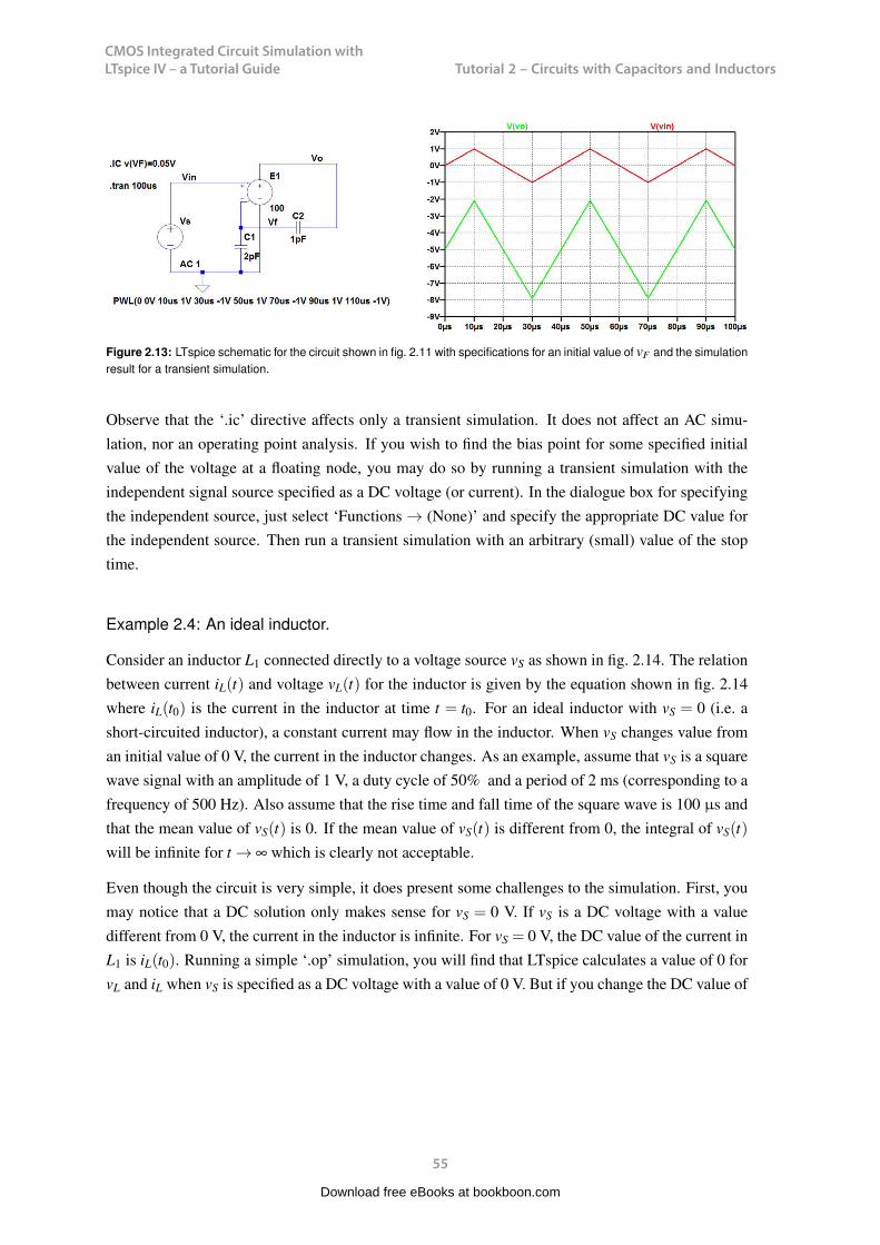
CMOS Integrated Circuit Simulation with LTspice IV – a Tutorial Guide
55
Tutorial 2 – Circuits with Capacitors and InductorsCMOS Integrated Circuit Simulation with LTspice IV Tutorial 2
Figure 2.13: LTspice schematic for the circuit shown in fig. 2.11 with specifications for an initial value of vF and the simulationresult for a transient simulation.
Observe that the ‘.ic’ directive affects only a transient simulation. It does not affect an AC simu-lation, nor an operating point analysis. If you wish to find the bias point for some specified initialvalue of the voltage at a floating node, you may do so by running a transient simulation with theindependent signal source specified as a DC voltage (or current). In the dialogue box for specifyingthe independent source, just select ‘Functions → (None)’ and specify the appropriate DC value forthe independent source. Then run a transient simulation with an arbitrary (small) value of the stoptime.
Example 2.4: An ideal inductor.
Consider an inductor L1 connected directly to a voltage source vS as shown in fig. 2.14. The relationbetween current iL(t) and voltage vL(t) for the inductor is given by the equation shown in fig. 2.14where iL(t0) is the current in the inductor at time t = t0. For an ideal inductor with vS = 0 (i.e. ashort-circuited inductor), a constant current may flow in the inductor. When vS changes value froman initial value of 0 V, the current in the inductor changes. As an example, assume that vS is a squarewave signal with an amplitude of 1 V, a duty cycle of 50% and a period of 2 ms (corresponding to afrequency of 500 Hz). Also assume that the rise time and fall time of the square wave is 100 µs andthat the mean value of vS(t) is 0. If the mean value of vS(t) is different from 0, the integral of vS(t)will be infinite for t → ∞ which is clearly not acceptable.
Even though the circuit is very simple, it does present some challenges to the simulation. First, youmay notice that a DC solution only makes sense for vS = 0 V. If vS is a DC voltage with a valuedifferent from 0 V, the current in the inductor is infinite. For vS = 0 V, the DC value of the current inL1 is iL(t0). Running a simple ‘.op’ simulation, you will find that LTspice calculates a value of 0 forvL and iL when vS is specified as a DC voltage with a value of 0 V. But if you change the DC value of
55
Download free eBooks at bookboon.com

CMOS Integrated Circuit Simulation with LTspice IV – a Tutorial Guide
56
Tutorial 2 – Circuits with Capacitors and InductorsCMOS Integrated Circuit Simulation with LTspice IV Tutorial 2
iL(t) =1L
∫ t
t0vL(t)dt + iL(t0)
Figure 2.14: An ideal inductor connected to a voltage source.
vS to some other value (e.g. 4 V), the ‘.op’ simulation will still run but it will not give a meaningfulresult for iL, and the error log does not give any warnings.
You may specify the value of iL(t0) using the ‘.ic’ SPICE Directive. For the ‘.op’ simulation, thisturns the inductor into a DC current source with the specified value of iL(t0), and the ‘.op’ simulationgives the correct result for iL(t0). Notice that the ‘.ic’ directive for the inductor current works with the‘.op’ command whereas the ‘.ic’ directive for a capacitor voltage does not work with ‘.op’ command.
Next, we will consider a transient simulation with the square wave voltage signal defined above. Weassume that the square wave is defined for all values of t (starts at −∞ and continues to +∞). For thetransient simulation, we may use the ‘Pulse’ function to specify the square wave. Fig. 2.15 showsthe LTspice schematic with a ‘Pulse’ specification for vS. The syntax for the ‘Pulse’ specification is
56
Download free eBooks at bookboon.com
Click on the ad to read moreClick on the ad to read moreClick on the ad to read moreClick on the ad to read moreClick on the ad to read moreClick on the ad to read moreClick on the ad to read moreClick on the ad to read moreClick on the ad to read moreClick on the ad to read moreClick on the ad to read moreClick on the ad to read moreClick on the ad to read moreClick on the ad to read moreClick on the ad to read moreClick on the ad to read moreClick on the ad to read moreClick on the ad to read moreClick on the ad to read more
EXPERIENCE THE POWER OF FULL ENGAGEMENT…
RUN FASTER. RUN LONGER.. RUN EASIER…
READ MORE & PRE-ORDER TODAY WWW.GAITEYE.COM
Challenge the way we run
1349906_A6_4+0.indd 1 22-08-2014 12:56:57
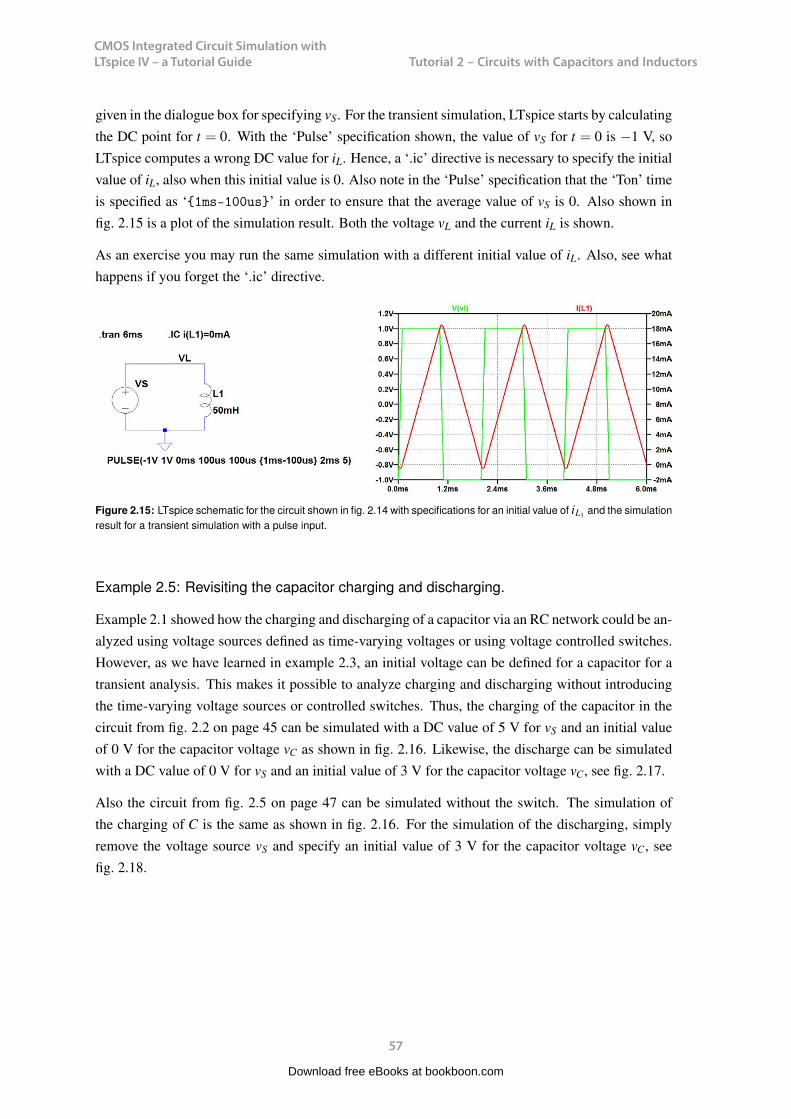
CMOS Integrated Circuit Simulation with LTspice IV – a Tutorial Guide
57
Tutorial 2 – Circuits with Capacitors and InductorsCMOS Integrated Circuit Simulation with LTspice IV Tutorial 2
given in the dialogue box for specifying vS. For the transient simulation, LTspice starts by calculatingthe DC point for t = 0. With the ‘Pulse’ specification shown, the value of vS for t = 0 is −1 V, soLTspice computes a wrong DC value for iL. Hence, a ‘.ic’ directive is necessary to specify the initialvalue of iL, also when this initial value is 0. Also note in the ‘Pulse’ specification that the ‘Ton’ timeis specified as ‘1ms-100us’ in order to ensure that the average value of vS is 0. Also shown infig. 2.15 is a plot of the simulation result. Both the voltage vL and the current iL is shown.
As an exercise you may run the same simulation with a different initial value of iL. Also, see whathappens if you forget the ‘.ic’ directive.
Figure 2.15: LTspice schematic for the circuit shown in fig. 2.14 with specifications for an initial value of iL1 and the simulationresult for a transient simulation with a pulse input.
Example 2.5: Revisiting the capacitor charging and discharging.
Example 2.1 showed how the charging and discharging of a capacitor via an RC network could be an-alyzed using voltage sources defined as time-varying voltages or using voltage controlled switches.However, as we have learned in example 2.3, an initial voltage can be defined for a capacitor for atransient analysis. This makes it possible to analyze charging and discharging without introducingthe time-varying voltage sources or controlled switches. Thus, the charging of the capacitor in thecircuit from fig. 2.2 on page 45 can be simulated with a DC value of 5 V for vS and an initial valueof 0 V for the capacitor voltage vC as shown in fig. 2.16. Likewise, the discharge can be simulatedwith a DC value of 0 V for vS and an initial value of 3 V for the capacitor voltage vC, see fig. 2.17.
Also the circuit from fig. 2.5 on page 47 can be simulated without the switch. The simulation ofthe charging of C is the same as shown in fig. 2.16. For the simulation of the discharging, simplyremove the voltage source vS and specify an initial value of 3 V for the capacitor voltage vC, seefig. 2.18.
Of course, a similar approach can be used for analyzing the magnetization and demagnetization of
57
Download free eBooks at bookboon.com
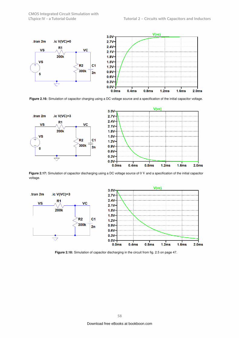
CMOS Integrated Circuit Simulation with LTspice IV – a Tutorial Guide
58
Tutorial 2 – Circuits with Capacitors and InductorsCMOS Integrated Circuit Simulation with LTspice IV Tutorial 2
Figure 2.16: Simulation of capacitor charging using a DC voltage source and a specification of the initial capacitor voltage.
Figure 2.17: Simulation of capacitor discharging using a DC voltage source of 0 V and a specification of the initial capacitorvoltage.
Figure 2.18: Simulation of capacitor discharging in the circuit from fig. 2.5 on page 47.
58
Download free eBooks at bookboon.com
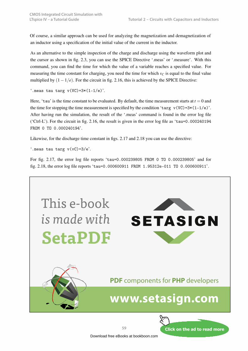
CMOS Integrated Circuit Simulation with LTspice IV – a Tutorial Guide
59
Tutorial 2 – Circuits with Capacitors and InductorsCMOS Integrated Circuit Simulation with LTspice IV Tutorial 2
an inductor using a specification of the initial value of the current in the inductor.
As an alternative to the simple inspection of the charge and discharge using the waveform plot andthe cursor as shown in fig. 2.3, you can use the SPICE Directive ‘.meas’ or ‘.measure’. With thiscommand, you can find the time for which the value of a variable reaches a specified value. Formeasuring the time constant for charging, you need the time for which vC is equal to the final valuemultiplied by (1−1/e). For the circuit in fig. 2.16, this is achieved by the SPICE Directive:
‘.meas tau targ v(VC)=3*(1-1/e)’.
Here, ‘tau’ is the time constant to be evaluated. By default, the time measurement starts at t = 0 andthe time for stopping the time measurement is specified by the condition ‘targ v(VC)=3*(1-1/e)’.After having run the simulation, the result of the ‘.meas’ command is found in the error log file(‘Ctrl-L’). For the circuit in fig. 2.16, the result is given in the error log file as ‘tau=0.000240194FROM 0 TO 0.000240194’.
Likewise, for the discharge time constant in figs. 2.17 and 2.18 you can use the directive:
‘.meas tau targ v(vC)=3/e’.
For fig. 2.17, the error log file reports ‘tau=0.000239805 FROM 0 TO 0.000239805’ and forfig. 2.18, the error log file reports ‘tau=0.000600911 FROM 1.95312e-011 TO 0.000600911’.
59
CMOS Integrated Circuit Simulation with LTspice IV Tutorial 2
given in the dialogue box for specifying vS. For the transient simulation, LTspice starts by calculatingthe DC point for t = 0. With the ‘Pulse’ specification shown, the value of vS for t = 0 is −1 V, soLTspice computes a wrong DC value for iL. Hence, a ‘.ic’ directive is necessary to specify the initialvalue of iL, also when this initial value is 0. Also note in the ‘Pulse’ specification that the ‘Ton’ timeis specified as ‘1ms-100us’ in order to ensure that the average value of vS is 0. Also shown infig. 2.15 is a plot of the simulation result. Both the voltage vL and the current iL is shown.
As an exercise you may run the same simulation with a different initial value of iL. Also, see whathappens if you forget the ‘.ic’ directive.
Figure 2.15: LTspice schematic for the circuit shown in fig. 2.14 with specifications for an initial value of iL1 and the simulationresult for a transient simulation with a pulse input.
Example 2.5: Revisiting the capacitor charging and discharging.
Example 2.1 showed how the charging and discharging of a capacitor via an RC network could be an-alyzed using voltage sources defined as time-varying voltages or using voltage controlled switches.However, as we have learned in example 2.3, an initial voltage can be defined for a capacitor for atransient analysis. This makes it possible to analyze charging and discharging without introducingthe time-varying voltage sources or controlled switches. Thus, the charging of the capacitor in thecircuit from fig. 2.2 on page 45 can be simulated with a DC value of 5 V for vS and an initial valueof 0 V for the capacitor voltage vC as shown in fig. 2.16. Likewise, the discharge can be simulatedwith a DC value of 0 V for vS and an initial value of 3 V for the capacitor voltage vC, see fig. 2.17.
Also the circuit from fig. 2.5 on page 47 can be simulated without the switch. The simulation ofthe charging of C is the same as shown in fig. 2.16. For the simulation of the discharging, simplyremove the voltage source vS and specify an initial value of 3 V for the capacitor voltage vC, seefig. 2.18.
Of course, a similar approach can be used for analyzing the magnetization and demagnetization of
57
Download free eBooks at bookboon.com
Click on the ad to read moreClick on the ad to read moreClick on the ad to read moreClick on the ad to read moreClick on the ad to read moreClick on the ad to read moreClick on the ad to read moreClick on the ad to read moreClick on the ad to read moreClick on the ad to read moreClick on the ad to read moreClick on the ad to read moreClick on the ad to read moreClick on the ad to read moreClick on the ad to read moreClick on the ad to read moreClick on the ad to read moreClick on the ad to read moreClick on the ad to read moreClick on the ad to read more
PDF components for PHP developers
www.setasign.com
SETASIGNThis e-book is made with SetaPDF

CMOS Integrated Circuit Simulation with LTspice IV – a Tutorial Guide
60
Tutorial 2 – Circuits with Capacitors and InductorsCMOS Integrated Circuit Simulation with LTspice IV Tutorial 2
The SPICE directive ‘.meas’ provides a very versatile possibility for post-processing of the simu-lation results. For details concerning the syntax of ‘.meas’, use the ‘help’ function in LTspice orsee (Brocard 2013). The command is particularly useful when several identical post-processingoperations are to be performed. Examples of this are demonstrated in Tutorial 6.
60
Download free eBooks at bookboon.com
CMOS Integrated Circuit Simulation with LTspice IV – a Tutorial Guide
61
Tutorial 2 – Circuits with Capacitors and InductorsCMOS Integrated Circuit Simulation with LTspice IV Tutorial 2
Hints and pitfalls
– Capacitors may give rise to floating nodes for DC voltages.
– For transient simulations, the value of a floating node may be specified using a ‘.ic’ SPICEDirective.
– For AC simulations and simulations of operating point (’.op’), a floating node may becontrolled by connecting a very large resistor from a non-floating node to the floating node.
– You cannot independently specify a DC voltage and a time varying signal for a voltagesource or current source.
– It can be a good idea to insert a signal source (voltage or current) as a combination of a DCbias source and a time varying signal source so that the DC bias value and the time varyingwaveform can be specified separately.
– LTspice is case insensitive. Thus, you cannot use uppercase and lowercase letters andsubscripts to distinguish between DC values, time varying signals and small signal values.
– The SPICE Error Log (‘Ctrl-L’) provides warnings about floating nodes.
– The initial value for a ‘.op’ simulation or a transient simulation of the current in an inductorcan be specified by a ‘.ic’ SPICE Directive.
– When specifying component values in the schematic, ‘e’ (or ‘E’) is used for specifying thesuffix, e.g. ‘e6’ for ‘Mega’.
– When specifying mathematical expressions in the waveform viewer, ‘e’ (or ‘E’) is the baseof the natural logarithm.
– Text and other annotations (e.g. cursor position) can be placed in a simulation plot usingthe command ‘Plot Settings → Notes & Annotations’.
– Curly brackets can be used to indicate expressions to be calculated by LTspice whenspecifying values, e.g. ‘2ms + 0.2us’ is equivalent to ‘2.0002ms’.
References
Brocard, G. 2013, The LTspice IV Simulator – Manual, Methods and Applications, First Edition,Swiridoff Verlag, Künzelsau, Germany.
Hambley, AR. 2014, Electrical Engineering, Principles and Applications, Sixth Edition, PearsonEducation Ltd., Harlow, UK.
61
Download free eBooks at bookboon.com

CMOS Integrated Circuit Simulation with LTspice IV – a Tutorial Guide
62
Tutorial 2 – Circuits with Capacitors and InductorsCMOS Integrated Circuit Simulation with LTspice IV Tutorial 2
Sedra, AS. & Smith, KC. 2011, Microelectronic Circuits, International Sixth Edition, Oxford Uni-versity Press, New York, USA.
62
Download free eBooks at bookboon.com
Click on the ad to read moreClick on the ad to read moreClick on the ad to read moreClick on the ad to read moreClick on the ad to read moreClick on the ad to read moreClick on the ad to read moreClick on the ad to read moreClick on the ad to read moreClick on the ad to read moreClick on the ad to read moreClick on the ad to read moreClick on the ad to read moreClick on the ad to read moreClick on the ad to read moreClick on the ad to read moreClick on the ad to read moreClick on the ad to read moreClick on the ad to read moreClick on the ad to read moreClick on the ad to read more
www.sylvania.com
We do not reinvent the wheel we reinvent light.Fascinating lighting offers an infinite spectrum of possibilities: Innovative technologies and new markets provide both opportunities and challenges. An environment in which your expertise is in high demand. Enjoy the supportive working atmosphere within our global group and benefit from international career paths. Implement sustainable ideas in close cooperation with other specialists and contribute to influencing our future. Come and join us in reinventing light every day.
Light is OSRAM
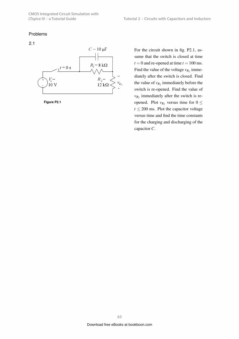
CMOS Integrated Circuit Simulation with LTspice IV – a Tutorial Guide
63
Tutorial 2 – Circuits with Capacitors and InductorsCMOS Integrated Circuit Simulation with LTspice IV Tutorial 2
Problems
2.1
Figure P2.1
For the circuit shown in fig. P2.1, as-sume that the switch is closed at timet = 0 and re-opened at time t = 100 ms.Find the value of the voltage vR2 imme-diately after the switch is closed. Findthe value of vR2 immediately before theswitch is re-opened. Find the value ofvR2 immediately after the switch is re-opened. Plot vR2 versus time for 0 ≤t ≤ 200 ms. Plot the capacitor voltageversus time and find the time constantsfor the charging and discharging of thecapacitor C.
63
Download free eBooks at bookboon.com
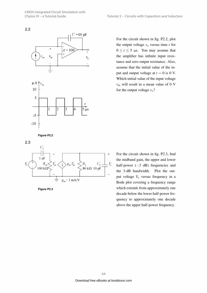
CMOS Integrated Circuit Simulation with LTspice IV – a Tutorial Guide
64
Tutorial 2 – Circuits with Capacitors and InductorsCMOS Integrated Circuit Simulation with LTspice IV Tutorial 2
2.2
Figure P2.2
For the circuit shown in fig. P2.2, plotthe output voltage vo versus time t for0 ≤ t ≤ 5 µs. You may assume thatthe amplifier has infinite input resis-tance and zero output resistance. Also,assume that the initial value of the in-put and output voltage at t = 0 is 0 V.Which initial value of the input voltagevin will result in a mean value of 0 Vfor the output voltage vo?
2.3
Figure P2.3
For the circuit shown in fig. P2.3, findthe midband gain, the upper and lowerhalf-power (−3 dB) frequencies andthe 3-dB bandwidth. Plot the out-put voltage Vo versus frequency in aBode plot covering a frequency rangewhich extends from approximately onedecade below the lower half-power fre-quency to approximately one decadeabove the upper half-power frequency.
64
Download free eBooks at bookboon.com
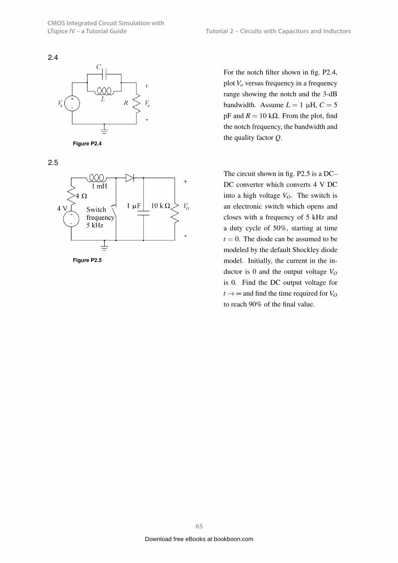
CMOS Integrated Circuit Simulation with LTspice IV – a Tutorial Guide
65
Tutorial 2 – Circuits with Capacitors and InductorsCMOS Integrated Circuit Simulation with LTspice IV Tutorial 2
2.4
Figure P2.4
For the notch filter shown in fig. P2.4,plot Vo versus frequency in a frequencyrange showing the notch and the 3-dBbandwidth. Assume L = 1 µH, C = 5pF and R = 10 kΩ. From the plot, findthe notch frequency, the bandwidth andthe quality factor Q.
2.5
Figure P2.5
The circuit shown in fig. P2.5 is a DC–DC converter which converts 4 V DCinto a high voltage VO. The switch isan electronic switch which opens andcloses with a frequency of 5 kHz anda duty cycle of 50%, starting at timet = 0. The diode can be assumed to bemodeled by the default Shockley diodemodel. Initially, the current in the in-ductor is 0 and the output voltage VO
is 0. Find the DC output voltage fort → ∞ and find the time required for VO
to reach 90% of the final value.
65
Download free eBooks at bookboon.com

CMOS Integrated Circuit Simulation with LTspice IV – a Tutorial Guide
66
Tutorial 2 – Circuits with Capacitors and InductorsCMOS Integrated Circuit Simulation with LTspice IV Tutorial 2
Answers
2.1: vR2(t=0) = 10 V; vR2(t=100 ms−) = 6.5 V; vR2(t=100 ms+) = 0 V; τ+ = 48 ms; τ− = 80 ms.
2.2: vin =−2.5 mV.
2.3: Midband gain: 38 dB. Lower half-power frequency: 1.59 kHz. Upper half-power frequency: 199kHz. 3-dB bandwidth: 197.4 kHz.
2.4: Notch frequency: 71.2 MHz, bandwidth: 3.18 MHz, quality factor Q = 22.4.
2.5: VO(t → ∞) = 51 V. Rise time: 7.5 ms.
66
Download free eBooks at bookboon.com
Click on the ad to read moreClick on the ad to read moreClick on the ad to read moreClick on the ad to read moreClick on the ad to read moreClick on the ad to read moreClick on the ad to read moreClick on the ad to read moreClick on the ad to read moreClick on the ad to read moreClick on the ad to read moreClick on the ad to read moreClick on the ad to read moreClick on the ad to read moreClick on the ad to read moreClick on the ad to read moreClick on the ad to read moreClick on the ad to read moreClick on the ad to read moreClick on the ad to read moreClick on the ad to read moreClick on the ad to read more
© Deloitte & Touche LLP and affiliated entities.
360°thinking.
Discover the truth at www.deloitte.ca/careers
© Deloitte & Touche LLP and affiliated entities.
360°thinking.
Discover the truth at www.deloitte.ca/careers
© Deloitte & Touche LLP and affiliated entities.
360°thinking.
Discover the truth at www.deloitte.ca/careers © Deloitte & Touche LLP and affiliated entities.
360°thinking.
Discover the truth at www.deloitte.ca/careers
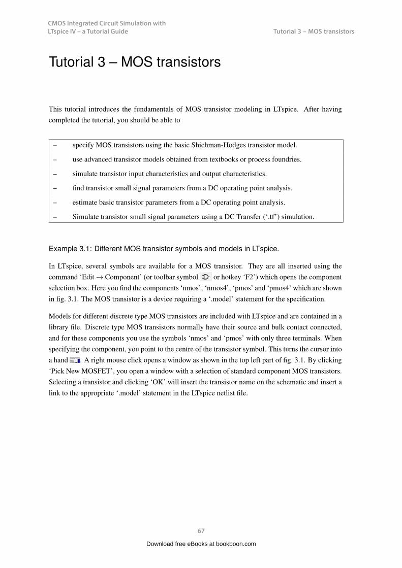
CMOS Integrated Circuit Simulation with LTspice IV – a Tutorial Guide
67
Tutorial 3 – MOS transistors
CMOS Integrated Circuit Simulation with LTspice IV Tutorial 3
Tutorial 3 – MOS transistors
This tutorial introduces the fundamentals of MOS transistor modeling in LTspice. After havingcompleted the tutorial, you should be able to
– specify MOS transistors using the basic Shichman-Hodges transistor model.
– use advanced transistor models obtained from textbooks or process foundries.
– simulate transistor input characteristics and output characteristics.
– find transistor small signal parameters from a DC operating point analysis.
– estimate basic transistor parameters from a DC operating point analysis.
– Simulate transistor small signal parameters using a DC Transfer (‘.tf’) simulation.
Example 3.1: Different MOS transistor symbols and models in LTspice.
In LTspice, several symbols are available for a MOS transistor. They are all inserted using thecommand ‘Edit → Component’ (or toolbar symbol or hotkey ‘F2’) which opens the componentselection box. Here you find the components ‘nmos’, ‘nmos4’, ‘pmos’ and ‘pmos4’ which are shownin fig. 3.1. The MOS transistor is a device requiring a ‘.model’ statement for the specification.
Models for different discrete type MOS transistors are included with LTspice and are contained in alibrary file. Discrete type MOS transistors normally have their source and bulk contact connected,and for these components you use the symbols ‘nmos’ and ‘pmos’ with only three terminals. Whenspecifying the component, you point to the centre of the transistor symbol. This turns the cursor intoa hand . A right mouse click opens a window as shown in the top left part of fig. 3.1. By clicking‘Pick New MOSFET’, you open a window with a selection of standard component MOS transistors.Selecting a transistor and clicking ‘OK’ will insert the transistor name on the schematic and insert alink to the appropriate ‘.model’ statement in the LTspice netlist file.
67
Download free eBooks at bookboon.com

CMOS Integrated Circuit Simulation with LTspice IV – a Tutorial Guide
68
Tutorial 3 – MOS transistorsCMOS Integrated Circuit Simulation with LTspice IV Tutorial 3
Figure 3.1: MOS transistor symbols and specification windows in LTspice.
Models for MOS transistors in integrated circuits are not included with LTspice. For MOS transistorsin integrated circuit design there is flexibility with respect to the bulk connection, so here you shoulduse the symbols ‘nmos4’ and ‘pmos4’ with four terminals. When right clicking on these symbols,a specification window as shown in the top right part of fig. 3.1 opens. Notice that the specification
68
Download free eBooks at bookboon.com
Click on the ad to read moreClick on the ad to read moreClick on the ad to read moreClick on the ad to read moreClick on the ad to read moreClick on the ad to read moreClick on the ad to read moreClick on the ad to read moreClick on the ad to read moreClick on the ad to read moreClick on the ad to read moreClick on the ad to read moreClick on the ad to read moreClick on the ad to read moreClick on the ad to read moreClick on the ad to read moreClick on the ad to read moreClick on the ad to read moreClick on the ad to read moreClick on the ad to read moreClick on the ad to read moreClick on the ad to read moreClick on the ad to read more
We will turn your CV into an opportunity of a lifetime
Do you like cars? Would you like to be a part of a successful brand?We will appreciate and reward both your enthusiasm and talent.Send us your CV. You will be surprised where it can take you.
Send us your CV onwww.employerforlife.com
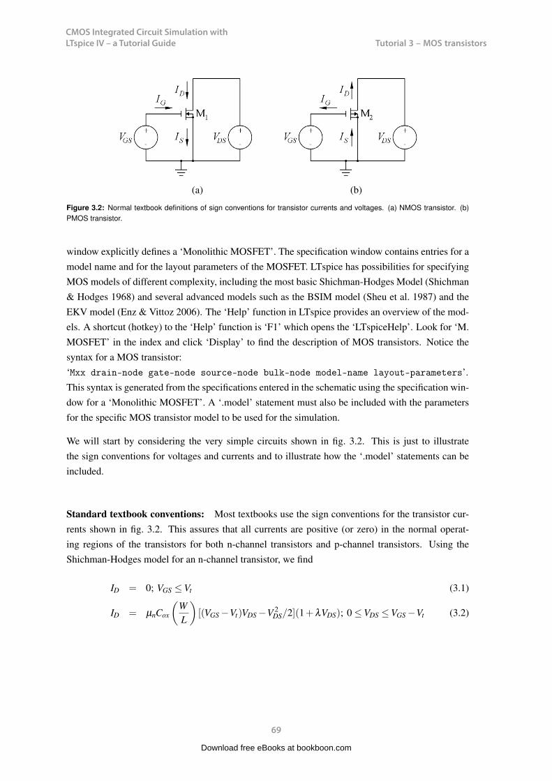
CMOS Integrated Circuit Simulation with LTspice IV – a Tutorial Guide
69
Tutorial 3 – MOS transistorsCMOS Integrated Circuit Simulation with LTspice IV Tutorial 3
(a) (b)
Figure 3.2: Normal textbook definitions of sign conventions for transistor currents and voltages. (a) NMOS transistor. (b)PMOS transistor.
window explicitly defines a ‘Monolithic MOSFET’. The specification window contains entries for amodel name and for the layout parameters of the MOSFET. LTspice has possibilities for specifyingMOS models of different complexity, including the most basic Shichman-Hodges Model (Shichman& Hodges 1968) and several advanced models such as the BSIM model (Sheu et al. 1987) and theEKV model (Enz & Vittoz 2006). The ‘Help’ function in LTspice provides an overview of the mod-els. A shortcut (hotkey) to the ‘Help’ function is ‘F1’ which opens the ‘LTspiceHelp’. Look for ‘M.MOSFET’ in the index and click ‘Display’ to find the description of MOS transistors. Notice thesyntax for a MOS transistor:‘Mxx drain-node gate-node source-node bulk-node model-name layout-parameters’.This syntax is generated from the specifications entered in the schematic using the specification win-dow for a ‘Monolithic MOSFET’. A ‘.model’ statement must also be included with the parametersfor the specific MOS transistor model to be used for the simulation.
We will start by considering the very simple circuits shown in fig. 3.2. This is just to illustratethe sign conventions for voltages and currents and to illustrate how the ‘.model’ statements can beincluded.
Standard textbook conventions: Most textbooks use the sign conventions for the transistor cur-rents shown in fig. 3.2. This assures that all currents are positive (or zero) in the normal operat-ing regions of the transistors for both n-channel transistors and p-channel transistors. Using theShichman-Hodges model for an n-channel transistor, we find
ID = 0; VGS ≤Vt (3.1)
ID = µnCox
(WL
)[(VGS −Vt)VDS −V 2
DS/2](1+λVDS); 0 ≤VDS ≤VGS −Vt (3.2)
69
Download free eBooks at bookboon.com
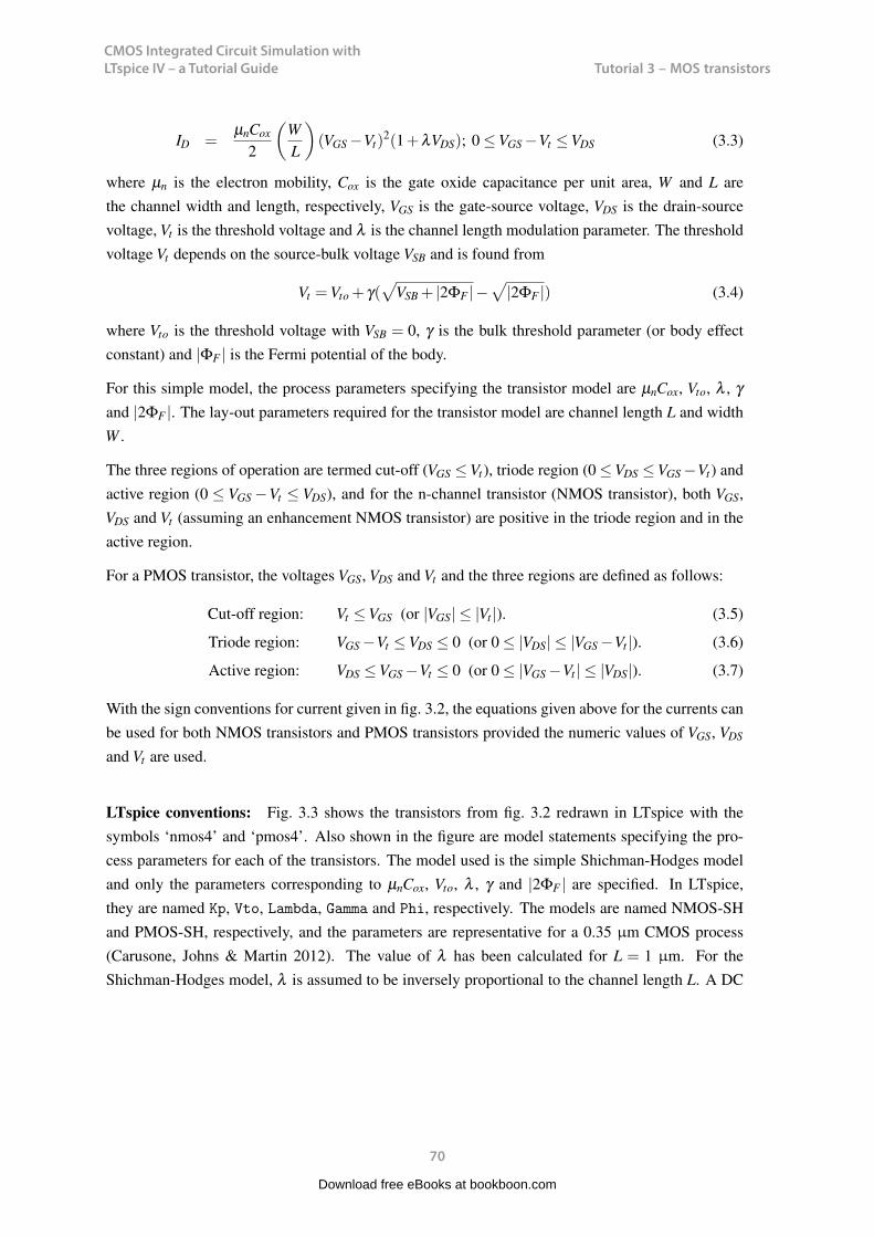
CMOS Integrated Circuit Simulation with LTspice IV – a Tutorial Guide
70
Tutorial 3 – MOS transistorsCMOS Integrated Circuit Simulation with LTspice IV Tutorial 3
ID =µnCox
2
(WL
)(VGS −Vt)
2(1+λVDS); 0 ≤VGS −Vt ≤VDS (3.3)
where µn is the electron mobility, Cox is the gate oxide capacitance per unit area, W and L arethe channel width and length, respectively, VGS is the gate-source voltage, VDS is the drain-sourcevoltage, Vt is the threshold voltage and λ is the channel length modulation parameter. The thresholdvoltage Vt depends on the source-bulk voltage VSB and is found from
Vt =Vto + γ(√
VSB + |2ΦF |−√|2ΦF |) (3.4)
where Vto is the threshold voltage with VSB = 0, γ is the bulk threshold parameter (or body effectconstant) and |ΦF | is the Fermi potential of the body.
For this simple model, the process parameters specifying the transistor model are µnCox, Vto, λ , γand |2ΦF |. The lay-out parameters required for the transistor model are channel length L and widthW .
The three regions of operation are termed cut-off (VGS ≤Vt), triode region (0 ≤VDS ≤VGS −Vt) andactive region (0 ≤ VGS −Vt ≤ VDS), and for the n-channel transistor (NMOS transistor), both VGS,VDS and Vt (assuming an enhancement NMOS transistor) are positive in the triode region and in theactive region.
For a PMOS transistor, the voltages VGS, VDS and Vt and the three regions are defined as follows:
Cut-off region: Vt ≤VGS (or |VGS| ≤ |Vt |). (3.5)
Triode region: VGS −Vt ≤VDS ≤ 0 (or 0 ≤ |VDS| ≤ |VGS −Vt |). (3.6)
Active region: VDS ≤VGS −Vt ≤ 0 (or 0 ≤ |VGS −Vt | ≤ |VDS|). (3.7)
With the sign conventions for current given in fig. 3.2, the equations given above for the currents canbe used for both NMOS transistors and PMOS transistors provided the numeric values of VGS, VDS
and Vt are used.
LTspice conventions: Fig. 3.3 shows the transistors from fig. 3.2 redrawn in LTspice with thesymbols ‘nmos4’ and ‘pmos4’. Also shown in the figure are model statements specifying the pro-cess parameters for each of the transistors. The model used is the simple Shichman-Hodges modeland only the parameters corresponding to µnCox, Vto, λ , γ and |2ΦF | are specified. In LTspice,they are named Kp, Vto, Lambda, Gamma and Phi, respectively. The models are named NMOS-SHand PMOS-SH, respectively, and the parameters are representative for a 0.35 µm CMOS process(Carusone, Johns & Martin 2012). The value of λ has been calculated for L = 1 µm. For theShichman-Hodges model, λ is assumed to be inversely proportional to the channel length L. A DC
70
Download free eBooks at bookboon.com

CMOS Integrated Circuit Simulation with LTspice IV – a Tutorial Guide
71
Tutorial 3 – MOS transistorsCMOS Integrated Circuit Simulation with LTspice IV Tutorial 3
Figure 3.3: LTspice schematic for the circuits from fig. 3.2.
operating point analysis is specified by the ‘.op’ command. The transistor geometries are specifiedusing the specification window shown in fig. 3.1, and for both transistors, L is 1 µm and W is 10µm. This specification is not visible on the schematic. To see this specification, use the command‘View → SPICE Netlist’ which brings up the window shown in the left part of fig. 3.4. Notice thatin addition to the circuit specification, the netlist includes references to the standard LTspice MOSmodels and the library file for standard MOS transistors.
Running the ‘.op’ simulation produces the output file shown in right part of fig. 3.4. From this, yousee that the drain current is positive for the NMOS transistor and negative for the PMOS transistor.
71
Download free eBooks at bookboon.com
Click on the ad to read moreClick on the ad to read moreClick on the ad to read moreClick on the ad to read moreClick on the ad to read moreClick on the ad to read moreClick on the ad to read moreClick on the ad to read moreClick on the ad to read moreClick on the ad to read moreClick on the ad to read moreClick on the ad to read moreClick on the ad to read moreClick on the ad to read moreClick on the ad to read moreClick on the ad to read moreClick on the ad to read moreClick on the ad to read moreClick on the ad to read moreClick on the ad to read moreClick on the ad to read moreClick on the ad to read moreClick on the ad to read moreClick on the ad to read more
Maersk.com/Mitas
e Graduate Programme for Engineers and Geoscientists
Month 16I was a construction
supervisor in the North Sea
advising and helping foremen
solve problems
I was a
hes
Real work International opportunities
ree work placementsal Internationaorree wo
I wanted real responsibili I joined MITAS because
www.discovermitas.com
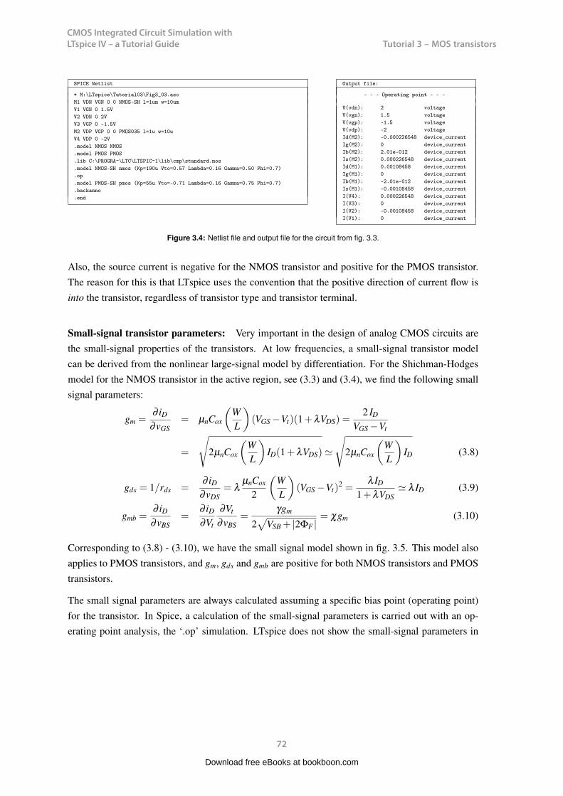
CMOS Integrated Circuit Simulation with LTspice IV – a Tutorial Guide
72
Tutorial 3 – MOS transistorsCMOS Integrated Circuit Simulation with LTspice IV Tutorial 3
SPICE Netlist
* M:\LTspice\Tutorial03\Fig3_03.ascM1 VDN VGN 0 0 NMOS-SH l=1um w=10umV1 VGN 0 1.5VV2 VDN 0 2VV3 VGP 0 -1.5VM2 VDP VGP 0 0 PMOS035 l=1u w=10uV4 VDP 0 -2V.model NMOS NMOS.model PMOS PMOS.lib C:\PROGRA~\LTC\LTSPIC~1\lib\cmp\standard.mos.model NMOS-SH nmos (Kp=190u Vto=0.57 Lambda=0.16 Gamma=0.50 Phi=0.7).op.model PMOS-SH pmos (Kp=55u Vto=-0.71 Lambda=0.16 Gamma=0.75 Phi=0.7).backanno.end
Output file:
- - - Operating point - - -
V(vdn): 2 voltageV(vgn): 1.5 voltageV(vgp): -1.5 voltageV(vdp): -2 voltageId(M2): -0.000226548 device_currentIg(M2): 0 device_currentIb(M2): 2.01e-012 device_currentIs(M2): 0.000226548 device_currentId(M1): 0.00108458 device_currentIg(M1): 0 device_currentIb(M1): -2.01e-012 device_currentIs(M1): -0.00108458 device_currentI(V4): 0.000226548 device_currentI(V3): 0 device_currentI(V2): -0.00108458 device_currentI(V1): 0 device_current
Figure 3.4: Netlist file and output file for the circuit from fig. 3.3.
Also, the source current is negative for the NMOS transistor and positive for the PMOS transistor.The reason for this is that LTspice uses the convention that the positive direction of current flow isinto the transistor, regardless of transistor type and transistor terminal.
Small-signal transistor parameters: Very important in the design of analog CMOS circuits arethe small-signal properties of the transistors. At low frequencies, a small-signal transistor modelcan be derived from the nonlinear large-signal model by differentiation. For the Shichman-Hodgesmodel for the NMOS transistor in the active region, see (3.3) and (3.4), we find the following smallsignal parameters:
gm =∂ iD
∂vGS= µnCox
(WL
)(VGS −Vt)(1+λVDS) =
2 ID
VGS −Vt
=
√2µnCox
(WL
)ID(1+λVDS)
√2µnCox
(WL
)ID (3.8)
gds = 1/rds =∂ iD
∂vDS= λ
µnCox
2
(WL
)(VGS −Vt)
2 =λ ID
1+λVDS λ ID (3.9)
gmb =∂ iD∂vBS
=∂ iD∂Vt
∂Vt
∂vBS=
γgm
2√
VSB + |2ΦF |= χgm (3.10)
Corresponding to (3.8) - (3.10), we have the small signal model shown in fig. 3.5. This model alsoapplies to PMOS transistors, and gm, gds and gmb are positive for both NMOS transistors and PMOStransistors.
The small signal parameters are always calculated assuming a specific bias point (operating point)for the transistor. In Spice, a calculation of the small-signal parameters is carried out with an op-erating point analysis, the ‘.op’ simulation. LTspice does not show the small-signal parameters in
72
Download free eBooks at bookboon.com
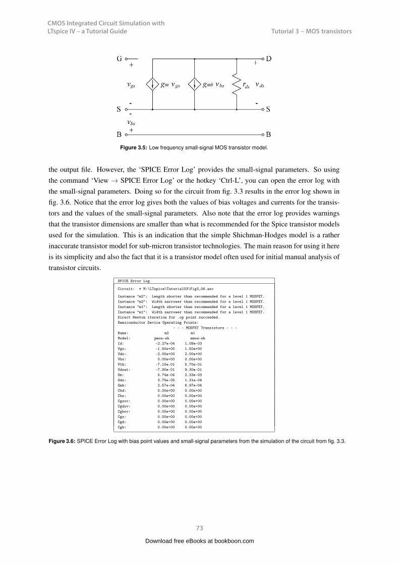
CMOS Integrated Circuit Simulation with LTspice IV – a Tutorial Guide
73
Tutorial 3 – MOS transistorsCMOS Integrated Circuit Simulation with LTspice IV Tutorial 3
Figure 3.5: Low frequency small-signal MOS transistor model.
the output file. However, the ‘SPICE Error Log’ provides the small-signal parameters. So usingthe command ‘View → SPICE Error Log’ or the hotkey ‘Ctrl-L’, you can open the error log withthe small-signal parameters. Doing so for the circuit from fig. 3.3 results in the error log shown infig. 3.6. Notice that the error log gives both the values of bias voltages and currents for the transis-tors and the values of the small-signal parameters. Also note that the error log provides warningsthat the transistor dimensions are smaller than what is recommended for the Spice transistor modelsused for the simulation. This is an indication that the simple Shichman-Hodges model is a ratherinaccurate transistor model for sub-micron transistor technologies. The main reason for using it hereis its simplicity and also the fact that it is a transistor model often used for initial manual analysis oftransistor circuits.
SPICE Error Log
Circuit: * M:\LTspice\Tutorial03\Fig3_06.asc
Instance "m2": Length shorter than recommended for a level 1 MOSFET.Instance "m2": Width narrower than recommended for a level 1 MOSFET.Instance "m1": Length shorter than recommended for a level 1 MOSFET.Instance "m1": Width narrower than recommended for a level 1 MOSFET.Direct Newton iteration for .op point succeeded.Semiconductor Device Operating Points:
- - - MOSFET Transistors - - -Name: m2 m1Model: pmos-sh nmos-shId: -2.27e-04 1.08e-03Vgs: -1.50e+00 1.50e+00Vds: -2.00e+00 2.00e+00Vbs: 0.00e+00 0.00e+00Vth: -7.10e-01 5.70e-01Vdsat: -7.90e-01 9.30e-01Gm: 5.74e-04 2.33e-03Gds: 2.75e-05 1.31e-04Gmb: 2.57e-04 6.97e-04Cbd: 0.00e+00 0.00e+00Cbs: 0.00e+00 0.00e+00Cgsov: 0.00e+00 0.00e+00Cgdov: 0.00e+00 0.00e+00Cgbov: 0.00e+00 0.00e+00Cgs: 0.00e+00 0.00e+00Cgd: 0.00e+00 0.00e+00Cgb: 0.00e+00 0.00e+00
Figure 3.6: SPICE Error Log with bias point values and small-signal parameters from the simulation of the circuit from fig. 3.3.
73
Download free eBooks at bookboon.com

CMOS Integrated Circuit Simulation with LTspice IV – a Tutorial Guide
74
Tutorial 3 – MOS transistorsCMOS Integrated Circuit Simulation with LTspice IV Tutorial 3
Figure 3.7: High frequency small-signal MOS transistor model.
At high frequencies, the small-signal model must be augmented with the internal capacitors of thetransistor as shown in fig. 3.7. The size of the capacitors is calculated from the transistor dimensions,including the channel length, the channel width and the dimensions of source diffusion and draindiffusion. Also gate overlap is considered. You will see that in fig. 3.6, all the capacitors have avalue of 0. In order to make it possible for LTspice to calculate the capacitances, the transistormodels must include parameters describing junction capacitances and oxide capacitance per unitarea and also overlap capacitances per unit length. The parameters are defined as shown in the
74
Download free eBooks at bookboon.com
Click on the ad to read moreClick on the ad to read moreClick on the ad to read moreClick on the ad to read moreClick on the ad to read moreClick on the ad to read moreClick on the ad to read moreClick on the ad to read moreClick on the ad to read moreClick on the ad to read moreClick on the ad to read moreClick on the ad to read moreClick on the ad to read moreClick on the ad to read moreClick on the ad to read moreClick on the ad to read moreClick on the ad to read moreClick on the ad to read moreClick on the ad to read moreClick on the ad to read moreClick on the ad to read moreClick on the ad to read moreClick on the ad to read moreClick on the ad to read moreClick on the ad to read more
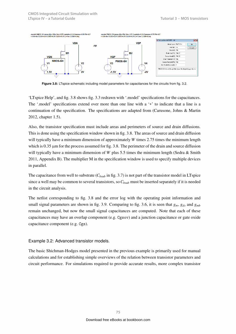
CMOS Integrated Circuit Simulation with LTspice IV – a Tutorial Guide
75
Tutorial 3 – MOS transistorsCMOS Integrated Circuit Simulation with LTspice IV Tutorial 3
Figure 3.8: LTspice schematic including model parameters for capacitances for the circuits from fig. 3.2.
‘LTspice Help’, and fig. 3.8 shows fig. 3.3 redrawn with ‘.model’ specifications for the capacitances.The ‘.model’ specifications extend over more than one line with a ‘+’ to indicate that a line is acontinuation of the specification. The specifications are adapted from (Carusone, Johns & Martin2012, chapter 1.5).
Also, the transistor specification must include areas and perimeters of source and drain diffusions.This is done using the specification window shown in fig. 3.8. The areas of source and drain diffusionwill typically have a minimum dimension of approximately W times 2.75 times the minimum lengthwhich is 0.35 µm for the process assumed for fig. 3.8. The perimeter of the drain and source diffusionwill typically have a minimum dimension of W plus 5.5 times the minimum length (Sedra & Smith2011, Appendix B). The multiplier M in the specification window is used to specify multiple devicesin parallel.
The capacitance from well to substrate (Cbsub in fig. 3.7) is not part of the transistor model in LTspicesince a well may be common to several transistors, so Cbsub must be inserted separately if it is neededin the circuit analysis.
The netlist corresponding to fig. 3.8 and the error log with the operating point information andsmall signal parameters are shown in fig. 3.9. Comparing to fig. 3.6, it is seen that gm, gds and gmb
remain unchanged, but now the small signal capacitances are computed. Note that each of thesecapacitances may have an overlap component (e.g. Cgsov) and a junction capacitance or gate oxidecapacitance component (e.g. Cgs).
Example 3.2: Advanced transistor models.
The basic Shichman-Hodges model presented in the previous example is primarily used for manualcalculations and for establishing simple overviews of the relation between transistor parameters andcircuit performance. For simulations required to provide accurate results, more complex transistor
75
Download free eBooks at bookboon.com
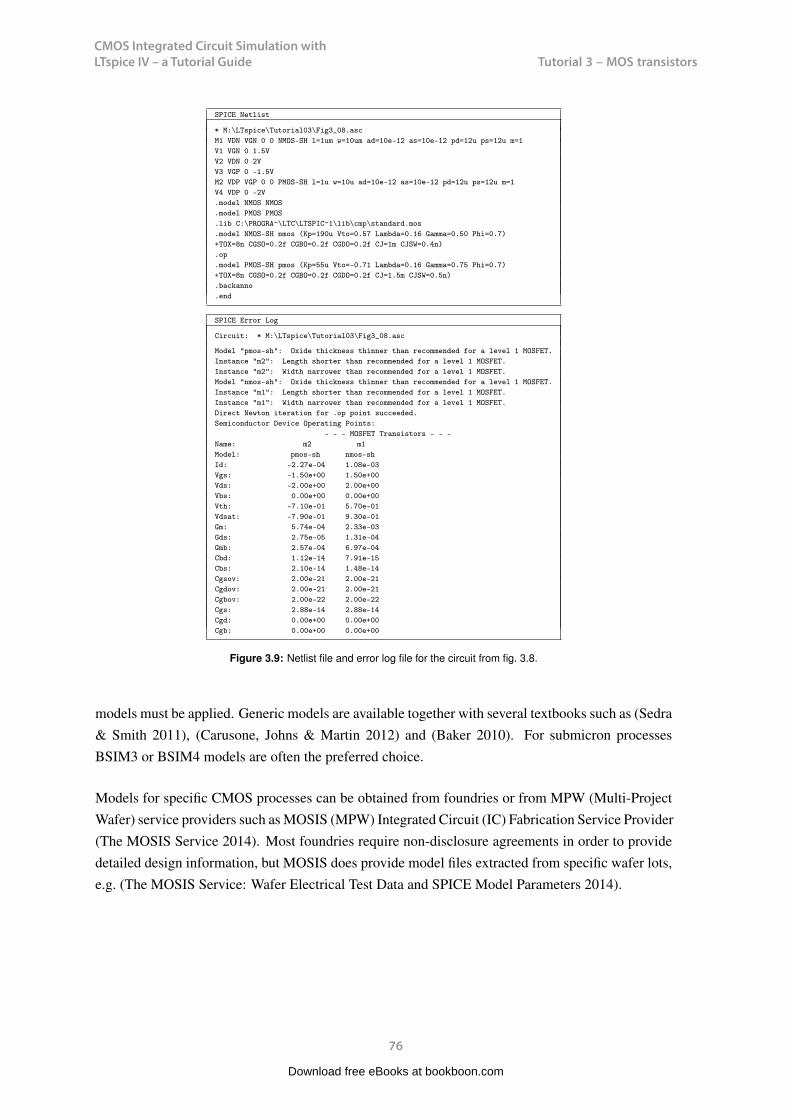
CMOS Integrated Circuit Simulation with LTspice IV – a Tutorial Guide
76
Tutorial 3 – MOS transistorsCMOS Integrated Circuit Simulation with LTspice IV Tutorial 3
SPICE Netlist
* M:\LTspice\Tutorial03\Fig3_08.ascM1 VDN VGN 0 0 NMOS-SH l=1um w=10um ad=10e-12 as=10e-12 pd=12u ps=12u m=1V1 VGN 0 1.5VV2 VDN 0 2VV3 VGP 0 -1.5VM2 VDP VGP 0 0 PMOS-SH l=1u w=10u ad=10e-12 as=10e-12 pd=12u ps=12u m=1V4 VDP 0 -2V.model NMOS NMOS.model PMOS PMOS.lib C:\PROGRA~\LTC\LTSPIC~1\lib\cmp\standard.mos.model NMOS-SH nmos (Kp=190u Vto=0.57 Lambda=0.16 Gamma=0.50 Phi=0.7)+TOX=8n CGSO=0.2f CGBO=0.2f CGDO=0.2f CJ=1m CJSW=0.4n).op.model PMOS-SH pmos (Kp=55u Vto=-0.71 Lambda=0.16 Gamma=0.75 Phi=0.7)+TOX=8n CGSO=0.2f CGBO=0.2f CGDO=0.2f CJ=1.5m CJSW=0.5n).backanno.end
SPICE Error Log
Circuit: * M:\LTspice\Tutorial03\Fig3_08.asc
Model "pmos-sh": Oxide thickness thinner than recommended for a level 1 MOSFET.Instance "m2": Length shorter than recommended for a level 1 MOSFET.Instance "m2": Width narrower than recommended for a level 1 MOSFET.Model "nmos-sh": Oxide thickness thinner than recommended for a level 1 MOSFET.Instance "m1": Length shorter than recommended for a level 1 MOSFET.Instance "m1": Width narrower than recommended for a level 1 MOSFET.Direct Newton iteration for .op point succeeded.Semiconductor Device Operating Points:
- - - MOSFET Transistors - - -Name: m2 m1Model: pmos-sh nmos-shId: -2.27e-04 1.08e-03Vgs: -1.50e+00 1.50e+00Vds: -2.00e+00 2.00e+00Vbs: 0.00e+00 0.00e+00Vth: -7.10e-01 5.70e-01Vdsat: -7.90e-01 9.30e-01Gm: 5.74e-04 2.33e-03Gds: 2.75e-05 1.31e-04Gmb: 2.57e-04 6.97e-04Cbd: 1.12e-14 7.91e-15Cbs: 2.10e-14 1.48e-14Cgsov: 2.00e-21 2.00e-21Cgdov: 2.00e-21 2.00e-21Cgbov: 2.00e-22 2.00e-22Cgs: 2.88e-14 2.88e-14Cgd: 0.00e+00 0.00e+00Cgb: 0.00e+00 0.00e+00
Figure 3.9: Netlist file and error log file for the circuit from fig. 3.8.
models must be applied. Generic models are available together with several textbooks such as (Sedra& Smith 2011), (Carusone, Johns & Martin 2012) and (Baker 2010). For submicron processesBSIM3 or BSIM4 models are often the preferred choice.
Models for specific CMOS processes can be obtained from foundries or from MPW (Multi-ProjectWafer) service providers such as MOSIS (MPW) Integrated Circuit (IC) Fabrication Service Provider(The MOSIS Service 2014). Most foundries require non-disclosure agreements in order to providedetailed design information, but MOSIS does provide model files extracted from specific wafer lots,e.g. (The MOSIS Service: Wafer Electrical Test Data and SPICE Model Parameters 2014).
76
Download free eBooks at bookboon.com
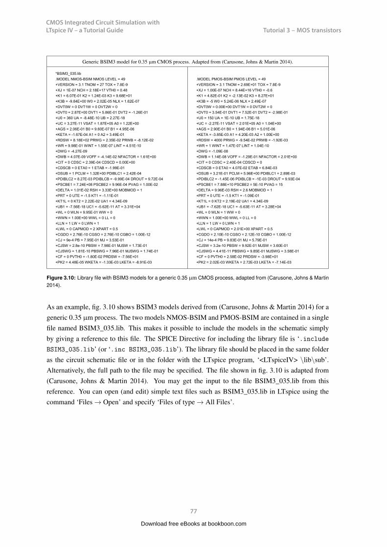
CMOS Integrated Circuit Simulation with LTspice IV – a Tutorial Guide
77
Tutorial 3 – MOS transistors
Generic BSIM3 model for 0.35 µm CMOS process. Adapted from (Carusone, Johns & Martin 2014).
*BSIM3_035.lib.MODEL NMOS-BSIM NMOS LEVEL = 49+VERSION = 3.1 TNOM = 27 TOX = 7.8E-9 +XJ = 1E-07 NCH = 2.18E+17 VTH0 = 0.48+K1 = 6.07E-01 K2 = 1.24E-03 K3 = 9.68E+01+K3B = -9.84E+00 W0 = 2.02E-05 NLX = 1.62E-07+DVT0W = 0 DVT1W = 0 DVT2W = 0+DVT0 = 2.87E+00 DVT1 = 5.86E-01 DVT2 = -1.26E-01+U0 = 360 UA = -8.48E-10 UB = 2.27E-18+UC = 3.27E-11 VSAT = 1.87E+05 A0 = 1.22E+00+AGS = 2.06E-01 B0 = 9.60E-07 B1 = 4.95E-06+KETA = -1.67E-04 A1 = 0 A2 = 3.49E-01+RDSW = 8.18E+02 PRWG = 2.35E-02 PRWB = -8.12E-02+WR = 9.98E-01 WINT = 1.55E-07 LINT = 4.51E-10+DWG = -4.27E-09+DWB = 4.07E-09 VOFF = -4.14E-02 NFACTOR = 1.61E+00+CIT = 0 CDSC = 2.39E-04 CDSCD = 0.00E+00+CDSCB = 0 ETA0 = 1 ETAB = -1.99E-01+DSUB = 1 PCLM = 1.32E+00 PDIBLC1 = 2.42E-04+PDIBLC2 = 8.27E-03 PDIBLCB = -9.99E-04 DROUT = 9.72E-04+PSCBE1 = 7.24E+08 PSCBE2 = 9.96E-04 PVAG = 1.00E-02+DELTA = 1.01E-02 RSH = 3.33E+00 MOBMOD = 1+PRT = 0 UTE = -1.5 KT1 = -1.11E-01+KT1L = 0 KT2 = 2.22E-02 UA1 = 4.34E-09+UB1 = -7.56E-18 UC1 = -5.62E-11 AT = 3.31E+04+WL = 0 WLN = 9.95E-01 WW = 0+WWN = 1.00E+00 WWL = 0 LL = 0+LLN = 1 LW = 0 LWN = 1+LWL = 0 CAPMOD = 2 XPART = 0.5+CGDO = 2.76E-10 CGSO = 2.76E-10 CGBO = 1.00E-12+CJ = 9e-4 PB = 7.95E-01 MJ = 3.53E-01+CJSW = 2.8e-10 PBSW = 7.98E-01 MJSW = 1.73E-01+CJSWG = 1.81E-10 PBSWG = 7.96E-01 MJSWG = 1.74E-01+CF = 0 PVTH0 = -1.80E-02 PRDSW = -7.56E+01+PK2 = 4.48E-05 WKETA = -1.33E-03 LKETA = -8.91E-03
.MODEL PMOS-BSIM PMOS LEVEL = 49+VERSION = 3.1 TNOM = 2.69E+01 TOX = 7.8E-9 +XJ = 1.00E-07 NCH = 8.44E+16 VTH0 = -0.6+K1 = 4.82E-01 K2 = -2.13E-02 K3 = 8.27E+01+K3B = -5 W0 = 5.24E-06 NLX = 2.49E-07+DVT0W = 0.00E+00 DVT1W = 0 DVT2W = 0+DVT0 = 3.54E-01 DVT1 = 7.52E-01 DVT2 = -2.98E-01+U0 = 150 UA = 1E-10 UB = 1.75E-18+UC = -2.27E-11 VSAT = 2.01E+05 A0 = 1.04E+00+AGS = 2.90E-01 B0 = 1.94E-06 B1 = 5.01E-06+KETA = -3.85E-03 A1 = 4.20E-03 A2 = 1.00E+00+RDSW = 4000 PRWG = -9.54E-02 PRWB = -1.92E-03+WR = 1 WINT = 1.47E-07 LINT = 1.04E-10+DWG = -1.09E-08+DWB = 1.14E-08 VOFF = -1.29E-01 NFACTOR = 2.01E+00+CIT = 0 CDSC = 2.40E-04 CDSCD = 0+CDSCB = 0 ETA0 = 4.07E-02 ETAB = 6.84E-03+DSUB = 3.21E-01 PCLM = 5.96E+00 PDIBLC1 = 2.89E-03+PDIBLC2 = -1.45E-06 PDIBLCB = -1E-03 DROUT = 9.93E-04+PSCBE1 = 7.88E+10 PSCBE2 = 5E-10 PVAG = 15+DELTA = 9.96E-03 RSH = 2.6 MOBMOD = 1+PRT = 0 UTE = -1.5 KT1 = -1.09E-01+KT1L = 0 KT2 = 2.19E-02 UA1 = 4.34E-09+UB1 = -7.62E-18 UC1 = -5.63E-11 AT = 3.28E+04+WL = 0 WLN = 1 WW = 0+WWN = 1.00E+00 WWL = 0 LL = 0+LLN = 1 LW = 0 LWN = 1+LWL = 0 CAPMOD = 2.01E+00 XPART = 0.5+CGDO = 2.10E-10 CGSO = 2.12E-10 CGBO = 1.00E-12+CJ = 14e-4 PB = 9.83E-01 MJ = 5.79E-01+CJSW = 3.2e-10 PBSW = 9.92E-01 MJSW = 3.60E-01+CJSWG = 4.41E-11 PBSWG = 9.85E-01 MJSWG = 3.58E-01+CF = 0 PVTH0 = 2.58E-02 PRDSW = -3.98E+01+PK2 = 2.02E-03 WKETA = 2.72E-03 LKETA = -7.14E-03
Figure 3.10: Library file with BSIM3 models for a generic 0.35 µm CMOS process, adapted from (Carusone, Johns & Martin2014).
As an example, fig. 3.10 shows BSIM3 models derived from (Carusone, Johns & Martin 2014) for ageneric 0.35 µm process. The two models NMOS-BSIM and PMOS-BSIM are contained in a singlefile named BSIM3_035.lib. This makes it possible to include the models in the schematic simplyby giving a reference to this file. The SPICE Directive for including the library file is ‘.includeBSIM3_035.lib’ (or ‘.inc BSIM3_035.lib’). The library file should be placed in the same folderas the circuit schematic file or in the folder with the LTspice program, ‘<LTspiceIV> \lib\sub’.Alternatively, the full path to the file may be specified. The file shown in fig. 3.10 is adapted from(Carusone, Johns & Martin 2014). You may get the input to the file BSIM3_035.lib from thisreference. You can open (and edit) simple text files such as BSIM3_035.lib in LTspice using thecommand ‘Files → Open’ and specify ‘Files of type → All Files’.
77Download free eBooks at bookboon.com

CMOS Integrated Circuit Simulation with LTspice IV – a Tutorial Guide
78
Tutorial 3 – MOS transistorsCMOS Integrated Circuit Simulation with LTspice IV Tutorial 3
ful to compare the results obtained from a simple model with the results from an advanced model inorder to explain deviations in circuit behavior from the manual calculations based on the Shichman-Hodges model. As a very simple example illustrating the differences, the circuit from fig. 3.8 maybe re-simulated with the models from the library file shown in fig. 3.10. This results in the netlistand error log file shown in fig. 3.11 which can be compared to fig. 3.9 on page 76.
You may observe that there are significant differences between the small-signal parameters shown infig. 3.9 and fig. 3.11 and it can be difficult to reach a reasonable degree of compliance between sim-ulated results and results based on a calculation from the Shichman-Hodges model. For comparison,(3.8) and (3.9) gives gm = 2.33 mA/V and gds = 131 µA/V for the NMOS transistor and gm = 0.574mA/V and gds = 27.5 µA/V for the PMOS transistor, corresponding exactly to the simulation resultsfrom fig. 3.9 but rather different from the values shown in fig. 3.11.
This illustrates a need for deriving useful Shichman-Hodges parameters from a transistor simulationbased on advanced models in order to be able to calculate analytical results which are useful forcircuit design. Also note that the BSIM3 model does not result in values for the small signal capac-itances in the same way as the Shichman-Hodges model, Rather, derivatives of charge with respectto signal voltages are specified. For a definition of the corresponding capacitances, see for instance(Tsividis & McAndrew 2010).
78
CMOS Integrated Circuit Simulation with LTspice IV Tutorial 3
Generic BSIM3 model for 0.35 µm CMOS process. Adapted from (Carusone, Johns & Martin 2014).
*BSIM3_035.lib.MODEL NMOS-BSIM NMOS LEVEL = 49+VERSION = 3.1 TNOM = 27 TOX = 7.8E-9 +XJ = 1E-07 NCH = 2.18E+17 VTH0 = 0.48+K1 = 6.07E-01 K2 = 1.24E-03 K3 = 9.68E+01+K3B = -9.84E+00 W0 = 2.02E-05 NLX = 1.62E-07+DVT0W = 0 DVT1W = 0 DVT2W = 0+DVT0 = 2.87E+00 DVT1 = 5.86E-01 DVT2 = -1.26E-01+U0 = 360 UA = -8.48E-10 UB = 2.27E-18+UC = 3.27E-11 VSAT = 1.87E+05 A0 = 1.22E+00+AGS = 2.06E-01 B0 = 9.60E-07 B1 = 4.95E-06+KETA = -1.67E-04 A1 = 0 A2 = 3.49E-01+RDSW = 8.18E+02 PRWG = 2.35E-02 PRWB = -8.12E-02+WR = 9.98E-01 WINT = 1.55E-07 LINT = 4.51E-10+DWG = -4.27E-09+DWB = 4.07E-09 VOFF = -4.14E-02 NFACTOR = 1.61E+00+CIT = 0 CDSC = 2.39E-04 CDSCD = 0.00E+00+CDSCB = 0 ETA0 = 1 ETAB = -1.99E-01+DSUB = 1 PCLM = 1.32E+00 PDIBLC1 = 2.42E-04+PDIBLC2 = 8.27E-03 PDIBLCB = -9.99E-04 DROUT = 9.72E-04+PSCBE1 = 7.24E+08 PSCBE2 = 9.96E-04 PVAG = 1.00E-02+DELTA = 1.01E-02 RSH = 3.33E+00 MOBMOD = 1+PRT = 0 UTE = -1.5 KT1 = -1.11E-01+KT1L = 0 KT2 = 2.22E-02 UA1 = 4.34E-09+UB1 = -7.56E-18 UC1 = -5.62E-11 AT = 3.31E+04+WL = 0 WLN = 9.95E-01 WW = 0+WWN = 1.00E+00 WWL = 0 LL = 0+LLN = 1 LW = 0 LWN = 1+LWL = 0 CAPMOD = 2 XPART = 0.5+CGDO = 2.76E-10 CGSO = 2.76E-10 CGBO = 1.00E-12+CJ = 9e-4 PB = 7.95E-01 MJ = 3.53E-01+CJSW = 2.8e-10 PBSW = 7.98E-01 MJSW = 1.73E-01+CJSWG = 1.81E-10 PBSWG = 7.96E-01 MJSWG = 1.74E-01+CF = 0 PVTH0 = -1.80E-02 PRDSW = -7.56E+01+PK2 = 4.48E-05 WKETA = -1.33E-03 LKETA = -8.91E-03
.MODEL PMOS-BSIM PMOS LEVEL = 49+VERSION = 3.1 TNOM = 2.69E+01 TOX = 7.8E-9 +XJ = 1.00E-07 NCH = 8.44E+16 VTH0 = -0.6+K1 = 4.82E-01 K2 = -2.13E-02 K3 = 8.27E+01+K3B = -5 W0 = 5.24E-06 NLX = 2.49E-07+DVT0W = 0.00E+00 DVT1W = 0 DVT2W = 0+DVT0 = 3.54E-01 DVT1 = 7.52E-01 DVT2 = -2.98E-01+U0 = 150 UA = 1E-10 UB = 1.75E-18+UC = -2.27E-11 VSAT = 2.01E+05 A0 = 1.04E+00+AGS = 2.90E-01 B0 = 1.94E-06 B1 = 5.01E-06+KETA = -3.85E-03 A1 = 4.20E-03 A2 = 1.00E+00+RDSW = 4000 PRWG = -9.54E-02 PRWB = -1.92E-03+WR = 1 WINT = 1.47E-07 LINT = 1.04E-10+DWG = -1.09E-08+DWB = 1.14E-08 VOFF = -1.29E-01 NFACTOR = 2.01E+00+CIT = 0 CDSC = 2.40E-04 CDSCD = 0+CDSCB = 0 ETA0 = 4.07E-02 ETAB = 6.84E-03+DSUB = 3.21E-01 PCLM = 5.96E+00 PDIBLC1 = 2.89E-03+PDIBLC2 = -1.45E-06 PDIBLCB = -1E-03 DROUT = 9.93E-04+PSCBE1 = 7.88E+10 PSCBE2 = 5E-10 PVAG = 15+DELTA = 9.96E-03 RSH = 2.6 MOBMOD = 1+PRT = 0 UTE = -1.5 KT1 = -1.09E-01+KT1L = 0 KT2 = 2.19E-02 UA1 = 4.34E-09+UB1 = -7.62E-18 UC1 = -5.63E-11 AT = 3.28E+04+WL = 0 WLN = 1 WW = 0+WWN = 1.00E+00 WWL = 0 LL = 0+LLN = 1 LW = 0 LWN = 1+LWL = 0 CAPMOD = 2.01E+00 XPART = 0.5+CGDO = 2.10E-10 CGSO = 2.12E-10 CGBO = 1.00E-12+CJ = 14e-4 PB = 9.83E-01 MJ = 5.79E-01+CJSW = 3.2e-10 PBSW = 9.92E-01 MJSW = 3.60E-01+CJSWG = 4.41E-11 PBSWG = 9.85E-01 MJSWG = 3.58E-01+CF = 0 PVTH0 = 2.58E-02 PRDSW = -3.98E+01+PK2 = 2.02E-03 WKETA = 2.72E-03 LKETA = -7.14E-03
Figure 3.10: Library file with BSIM3 models for a generic 0.35 µm CMOS process, adapted from (Carusone, Johns & Martin2014).
As an example, fig. 3.10 shows BSIM3 models derived from (Carusone, Johns & Martin 2014) for ageneric 0.35 µm process. The two models NMOS-BSIM and PMOS-BSIM are contained in a singlefile named BSIM3_035.lib. This makes it possible to include the models in the schematic simplyby giving a reference to this file. The SPICE Directive for including the library file is ‘.includeBSIM3_035.lib’ (or ‘.inc BSIM3_035.lib’). The library file should be placed in the same folderas the circuit schematic file or in the folder with the LTspice program, ‘<LTspiceIV> \lib\sub’.Alternatively, the full path to the file may be specified. The file shown in fig. 3.10 is adapted from(Carusone, Johns & Martin 2014). You may get the input to the file BSIM3_035.lib from thisreference, or you may directly copy from fig. 3.10 into a text editor (e.g. Notepad) and save thefile as BSIM3_035.lib. You can open (and edit) simple text files such as BSIM3_035.lib in LTspiceusing the command ‘Files → Open’ and specify ‘Files of type → All Files’.
Using more advanced models will generally give more precise simulation results, and often it is use-
77
Download free eBooks at bookboon.com
Click on the ad to read moreClick on the ad to read moreClick on the ad to read moreClick on the ad to read moreClick on the ad to read moreClick on the ad to read moreClick on the ad to read moreClick on the ad to read moreClick on the ad to read moreClick on the ad to read moreClick on the ad to read moreClick on the ad to read moreClick on the ad to read moreClick on the ad to read moreClick on the ad to read moreClick on the ad to read moreClick on the ad to read moreClick on the ad to read moreClick on the ad to read moreClick on the ad to read moreClick on the ad to read moreClick on the ad to read moreClick on the ad to read moreClick on the ad to read moreClick on the ad to read moreClick on the ad to read more
STUDY AT A TOP RANKED INTERNATIONAL BUSINESS SCHOOL
Reach your full potential at the Stockholm School of Economics, in one of the most innovative cities in the world. The School is ranked by the Financial Times as the number one business school in the Nordic and Baltic countries.
Visit us at www.hhs.se
Swed
en
Stockholm
no.1nine years in a row
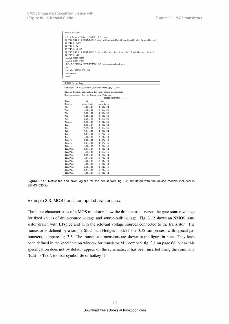
CMOS Integrated Circuit Simulation with LTspice IV – a Tutorial Guide
79
Tutorial 3 – MOS transistorsCMOS Integrated Circuit Simulation with LTspice IV Tutorial 3
SPICE Netlist
* M:\LTspice\Tutorial03\Fig3_11.ascM1 VDN VGN 0 0 NMOS-BSIM l=1um w=10um ad=10e-12 as=10e-12 pd=12u ps=12u m=1V1 VGN 0 1.5VV2 VDN 0 2VV3 VGP 0 -1.5VM2 VDP VGP 0 0 PMOS-BSIM l=1u w=10u ad=10e-12 as=10e-12 pd=12u ps=12u m=1V4 VDP 0 -2V.model NMOS NMOS.model PMOS PMOS.lib C:\PROGRA~\LTC\LTSPIC~1\lib\cmp\standard.mos.opinclude BSIM3_035.lib.backanno.end
SPICE Error Log
Circuit: * M:\LTspice\Tutorial03\Fig3_11.asc
Direct Newton iteration for .op point succeeded.Semiconductor Device Operating Points:
- - - BSIM3 MOSFETS - - -Name: m2 m1Model: pmos-bsim nmos-bsimId: -1.60e-04 5.48e-04Vgs: -1.50e+00 1.50e+00Vds: -2.00e+00 2.00e+00Vbs: 0.00e+00 0.00e+00Vth: -6.79e-01 5.43e-01Vdsat: -6.96e-01 6.21e-01Gm: 3.39e-04 9.92e-04Gds: 7.31e-06 1.03e-05Gmb: 7.54e-05 2.63e-04Cbd: 8.14e-15 7.70e-15Cbs: 1.52e-14 1.14e-14Cgsov: 2.06e-15 2.67e-15Cgdov: 2.04e-15 2.67e-15Cgbov: 1.00e-18 9.99e-19dQgdVgb: 3.81e-14 3.99e-14dQgdVdb: -1.99e-15 -2.68e-15dQgdVsb: -3.43e-14 -3.59e-14dQddVgb: -1.64e-14 -1.70e-14dQddVdb: 1.02e-14 1.04e-14dQddVsb: 1.79e-14 1.90e-14dQbdVgb: -5.36e-15 -6.01e-15dQbdVdb: -8.14e-15 -7.71e-15dQbdVsb: -1.88e-14 -1.62e-14
Figure 3.11: Netlist file and error log file for the circuit from fig. 3.8 simulated with the device models included inBSIM3_035.lib.
Example 3.3: MOS transistor input characteristics.
The input characteristics of a MOS transistor show the drain current versus the gate-source voltagefor fixed values of drain-source voltage and source-bulk voltage. Fig. 3.12 shows an NMOS tran-sistor drawn with LTspice and with the relevant voltage sources connected to the transistor. Thetransistor is defined by a simple Shichman-Hodges model for a 0.35 µm process with typical pa-rameters, compare fig. 3.3. The transistor dimensions are shown in the figure in blue. They havebeen defined in the specification window for transistor M1, compare fig. 3.1 on page 68, but as thisspecification does not by default appear on the schematic, it has been inserted using the command‘Edit → Text’, toolbar symbol or hotkey ‘T’.
79
Download free eBooks at bookboon.com

CMOS Integrated Circuit Simulation with LTspice IV – a Tutorial Guide
80
Tutorial 3 – MOS transistorsCMOS Integrated Circuit Simulation with LTspice IV Tutorial 3
Figure 3.12: LTspice schematic for simulation of transistor characteristics.
In the LTspice netlist, the text appears as a comment, i.e. a line starting with an asterix (*). This isa ‘quick and dirty’ way of showing the transistor dimensions because there is nothing to ensure thatthe comment matches the transistor specification, but it will do for now when we are consideringjust a single transistor. In circuits with more transistors, it is highly advisable to show the transistorspecification in a way that annotates to the netlist. On page 106, it is explained how to do this.
When simulating the transistor characteristics for a transistor to be applied in a circuit design, it isimportant to use transistor dimensions, in particular channel length, corresponding to the dimensionsplanned to be used for the circuit design, and when modifying the channel length, the value of λ
80
CMOS Integrated Circuit Simulation with LTspice IV Tutorial 3
Figure 3.13: Plot of ID versus VGS for different values of VDS and VSB = 0 V.
should also be re-calculated since λ is inversely proportional to the channel length L.
First, the drain current is simulated versus the gate-source voltage with VSB = 0 and with VDS varyingin steps of 0.5 V from 0 to 3 V. The simulation command for this is the ‘.dc’ command with thevoltage source V1 as the first source and V2 as the second source. The voltage V1 is specified tosweep from 0 to 3 V with an increment of 0.01 V in order to obtain a reasonably smooth curveshowing ID and the derivative of ID with respect to VGS. The resulting plot of ID versus VGS is shownin fig. 3.13.
The plot shows seven curves corresponding to VDS = 0, 0.5, 1.0, 1.5, 2.0, 2.5 and 3.0 V, respec-tively. In the plot, labels have been inserted for two of the curves using the command ‘Plot Settings→ Notes & Annotations → Place Text’. For the two curves corresponding to VDS = 2.5 V and 3.0 V,the transistor is in the active region for the simulated range of VGS, and the curves show a parabolicrelation between ID and VGS. For the other values of VDS, the transistor is in the triode region forlarge values of VGS, leading to a linear relation between ID and VGS.
As explained for fig. 2.3 on page 46, a cursor can be activated by a left mouse click on the tracelabel above the plot window. The cursor opens with a horizontal value in the middle of the plot (i.e.VGS = 1.5 V) and is attached to the first trace, i.e. the trace corresponding to VDS = 0 V. The cursormay be moved to the other traces by positioning the mouse over the cursor (a ‘1’ will appear on theplot) and entering the ‘up’ arrow key on the keyboard. By using the arrow keys ‘up’ and ‘down’, thecursor can be moved between the traces. A right mouse click when the mouse is positioned over thecursor will open a window with cursor step information, i.e. information about the trace where thecursor is attached. Also, when a cursor is included in the plot, a window is open with informationabout the position of the cursor, compare fig. 2.3 (page 46).
Next, fig. 3.14 shows the derivative of ID versus VGS. This is obtained from the same simulation, just
81
Download free eBooks at bookboon.com
Click on the ad to read moreClick on the ad to read moreClick on the ad to read moreClick on the ad to read moreClick on the ad to read moreClick on the ad to read moreClick on the ad to read moreClick on the ad to read moreClick on the ad to read moreClick on the ad to read moreClick on the ad to read moreClick on the ad to read moreClick on the ad to read moreClick on the ad to read moreClick on the ad to read moreClick on the ad to read moreClick on the ad to read moreClick on the ad to read moreClick on the ad to read moreClick on the ad to read moreClick on the ad to read moreClick on the ad to read moreClick on the ad to read moreClick on the ad to read moreClick on the ad to read moreClick on the ad to read moreClick on the ad to read more
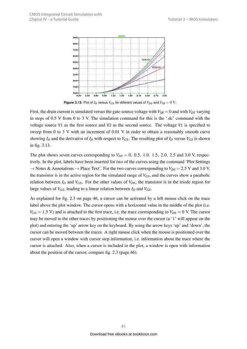
CMOS Integrated Circuit Simulation with LTspice IV – a Tutorial Guide
81
Tutorial 3 – MOS transistorsCMOS Integrated Circuit Simulation with LTspice IV Tutorial 3
Figure 3.13: Plot of ID versus VGS for different values of VDS and VSB = 0 V.
should also be re-calculated since λ is inversely proportional to the channel length L.
First, the drain current is simulated versus the gate-source voltage with VSB = 0 and with VDS varyingin steps of 0.5 V from 0 to 3 V. The simulation command for this is the ‘.dc’ command with thevoltage source V1 as the first source and V2 as the second source. The voltage V1 is specified tosweep from 0 to 3 V with an increment of 0.01 V in order to obtain a reasonably smooth curveshowing ID and the derivative of ID with respect to VGS. The resulting plot of ID versus VGS is shownin fig. 3.13.
The plot shows seven curves corresponding to VDS = 0, 0.5, 1.0, 1.5, 2.0, 2.5 and 3.0 V, respec-tively. In the plot, labels have been inserted for two of the curves using the command ‘Plot Settings→ Notes & Annotations → Place Text’. For the two curves corresponding to VDS = 2.5 V and 3.0 V,the transistor is in the active region for the simulated range of VGS, and the curves show a parabolicrelation between ID and VGS. For the other values of VDS, the transistor is in the triode region forlarge values of VGS, leading to a linear relation between ID and VGS.
As explained for fig. 2.3 on page 46, a cursor can be activated by a left mouse click on the tracelabel above the plot window. The cursor opens with a horizontal value in the middle of the plot (i.e.VGS = 1.5 V) and is attached to the first trace, i.e. the trace corresponding to VDS = 0 V. The cursormay be moved to the other traces by positioning the mouse over the cursor (a ‘1’ will appear on theplot) and entering the ‘up’ arrow key on the keyboard. By using the arrow keys ‘up’ and ‘down’, thecursor can be moved between the traces. A right mouse click when the mouse is positioned over thecursor will open a window with cursor step information, i.e. information about the trace where thecursor is attached. Also, when a cursor is included in the plot, a window is open with informationabout the position of the cursor, compare fig. 2.3 (page 46).
Next, fig. 3.14 shows the derivative of ID versus VGS. This is obtained from the same simulation, just
81
CMOS Integrated Circuit Simulation with LTspice IV Tutorial 3
Figure 3.13: Plot of ID versus VGS for different values of VDS and VSB = 0 V.
should also be re-calculated since λ is inversely proportional to the channel length L.
First, the drain current is simulated versus the gate-source voltage with VSB = 0 and with VDS varyingin steps of 0.5 V from 0 to 3 V. The simulation command for this is the ‘.dc’ command with thevoltage source V1 as the first source and V2 as the second source. The voltage V1 is specified tosweep from 0 to 3 V with an increment of 0.01 V in order to obtain a reasonably smooth curveshowing ID and the derivative of ID with respect to VGS. The resulting plot of ID versus VGS is shownin fig. 3.13.
The plot shows seven curves corresponding to VDS = 0, 0.5, 1.0, 1.5, 2.0, 2.5 and 3.0 V, respec-tively. In the plot, labels have been inserted for two of the curves using the command ‘Plot Settings→ Notes & Annotations → Place Text’. For the two curves corresponding to VDS = 2.5 V and 3.0 V,the transistor is in the active region for the simulated range of VGS, and the curves show a parabolicrelation between ID and VGS. For the other values of VDS, the transistor is in the triode region forlarge values of VGS, leading to a linear relation between ID and VGS.
As explained for fig. 2.3 on page 46, a cursor can be activated by a left mouse click on the tracelabel above the plot window. The cursor opens with a horizontal value in the middle of the plot (i.e.VGS = 1.5 V) and is attached to the first trace, i.e. the trace corresponding to VDS = 0 V. The cursormay be moved to the other traces by positioning the mouse over the cursor (a ‘1’ will appear on theplot) and entering the ‘up’ arrow key on the keyboard. By using the arrow keys ‘up’ and ‘down’, thecursor can be moved between the traces. A right mouse click when the mouse is positioned over thecursor will open a window with cursor step information, i.e. information about the trace where thecursor is attached. Also, when a cursor is included in the plot, a window is open with informationabout the position of the cursor, compare fig. 2.3 (page 46).
Next, fig. 3.14 shows the derivative of ID versus VGS. This is obtained from the same simulation, just
81
Download free eBooks at bookboon.com
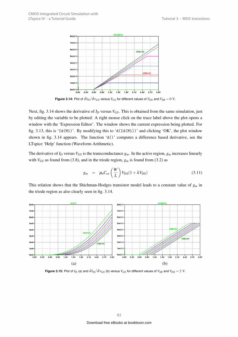
CMOS Integrated Circuit Simulation with LTspice IV – a Tutorial Guide
82
Tutorial 3 – MOS transistorsCMOS Integrated Circuit Simulation with LTspice IV Tutorial 3
Figure 3.14: Plot of ∂ iD/∂vGS versus VGS for different values of VDS and VSB = 0 V.
by editing the variable to be plotted: A right mouse click on the trace label above the plot opens awindow with the ‘Expression Editor’. The window shows the current expression being plotted. Forfig. 3.13, this is ‘Id(M1)’. By modifying this to ‘d(Id(M1))’ and clicking ‘OK’, the plot windowshown in fig. 3.14 appears. The function ‘d()’ computes a difference based derivative, see theLTspice ‘Help’ function (Waveform Arithmetic).
The derivative of ID versus VGS is the transconductance gm. In the active region, gm increases linearlywith VGS as found from (3.8), and in the triode region, gm is found from (3.2) as
gm = µnCox
(WL
)VDS(1+λVDS) (3.11)
This relation shows that the Shichman-Hodges transistor model leads to a constant value of gm inthe triode region as also clearly seen in fig. 3.14.
(a) (b)
Figure 3.15: Plot of ID (a) and ∂ iD/∂vGS (b) versus VGS for different values of VSB and VDS = 2 V.
82
CMOS Integrated Circuit Simulation with LTspice IV Tutorial 3
Figure 3.13: Plot of ID versus VGS for different values of VDS and VSB = 0 V.
should also be re-calculated since λ is inversely proportional to the channel length L.
First, the drain current is simulated versus the gate-source voltage with VSB = 0 and with VDS varyingin steps of 0.5 V from 0 to 3 V. The simulation command for this is the ‘.dc’ command with thevoltage source V1 as the first source and V2 as the second source. The voltage V1 is specified tosweep from 0 to 3 V with an increment of 0.01 V in order to obtain a reasonably smooth curveshowing ID and the derivative of ID with respect to VGS. The resulting plot of ID versus VGS is shownin fig. 3.13.
The plot shows seven curves corresponding to VDS = 0, 0.5, 1.0, 1.5, 2.0, 2.5 and 3.0 V, respec-tively. In the plot, labels have been inserted for two of the curves using the command ‘Plot Settings→ Notes & Annotations → Place Text’. For the two curves corresponding to VDS = 2.5 V and 3.0 V,the transistor is in the active region for the simulated range of VGS, and the curves show a parabolicrelation between ID and VGS. For the other values of VDS, the transistor is in the triode region forlarge values of VGS, leading to a linear relation between ID and VGS.
As explained for fig. 2.3 on page 46, a cursor can be activated by a left mouse click on the tracelabel above the plot window. The cursor opens with a horizontal value in the middle of the plot (i.e.VGS = 1.5 V) and is attached to the first trace, i.e. the trace corresponding to VDS = 0 V. The cursormay be moved to the other traces by positioning the mouse over the cursor (a ‘1’ will appear on theplot) and entering the ‘up’ arrow key on the keyboard. By using the arrow keys ‘up’ and ‘down’, thecursor can be moved between the traces. A right mouse click when the mouse is positioned over thecursor will open a window with cursor step information, i.e. information about the trace where thecursor is attached. Also, when a cursor is included in the plot, a window is open with informationabout the position of the cursor, compare fig. 2.3 (page 46).
Next, fig. 3.14 shows the derivative of ID versus VGS. This is obtained from the same simulation, just
81
CMOS Integrated Circuit Simulation with LTspice IV Tutorial 3
Figure 3.14: Plot of ∂ iD/∂vGS versus VGS for different values of VDS and VSB = 0 V.
by editing the variable to be plotted: A right mouse click on the trace label above the plot opens awindow with the ‘Expression Editor’. The window shows the current expression being plotted. Forfig. 3.13, this is ‘Id(M1)’. By modifying this to ‘d(Id(M1))’ and clicking ‘OK’, the plot windowshown in fig. 3.14 appears. The function ‘d()’ computes a difference based derivative, see theLTspice ‘Help’ function (Waveform Arithmetic).
The derivative of ID versus VGS is the transconductance gm. In the active region, gm increases linearlywith VGS as found from (3.8), and in the triode region, gm is found from (3.2) as
gm = µnCox
(WL
)VDS(1+λVDS) (3.11)
This relation shows that the Shichman-Hodges transistor model leads to a constant value of gm inthe triode region as also clearly seen in fig. 3.14.
(a) (b)
Figure 3.15: Plot of ID (a) and ∂ iD/∂vGS (b) versus VGS for different values of VSB and VDS = 2 V.
82
Download free eBooks at bookboon.com

CMOS Integrated Circuit Simulation with LTspice IV – a Tutorial Guide
83
Tutorial 3 – MOS transistorsCMOS Integrated Circuit Simulation with LTspice IV Tutorial 3
Next, we may investigate the influence of the source-bulk voltage VSB. For the previous simulations,VSB was equal to 0 but as indicated by (3.4), a positive value of VSB, reverse biasing the channel-bulk junction, will lead to an increase in the threshold voltage Vt . Fig. 3.15 shows a plot of ID and∂ iD/∂vGS versus VGS with a fixed value of 2 V for VDS and VSB swept from 0 to 3 V in steps of 0.5V. The shift of the curves caused by the increase of the threshold voltage is obvious.
As indicated by (3.10), the bulk terminal may also be used as the input signal to the transistorinstead of the gate terminal. An increase in VSB causes a decrease in ID for a fixed value of VGS
(a) (b)
Figure 3.16: Plot ID (a) and ∂ iD/∂vBS (b) versus VSB for different values of VDS and VGS = 1.5 V.
83
Download free eBooks at bookboon.com
Click on the ad to read moreClick on the ad to read moreClick on the ad to read moreClick on the ad to read moreClick on the ad to read moreClick on the ad to read moreClick on the ad to read moreClick on the ad to read moreClick on the ad to read moreClick on the ad to read moreClick on the ad to read moreClick on the ad to read moreClick on the ad to read moreClick on the ad to read moreClick on the ad to read moreClick on the ad to read moreClick on the ad to read moreClick on the ad to read moreClick on the ad to read moreClick on the ad to read moreClick on the ad to read moreClick on the ad to read moreClick on the ad to read moreClick on the ad to read moreClick on the ad to read moreClick on the ad to read moreClick on the ad to read moreClick on the ad to read more
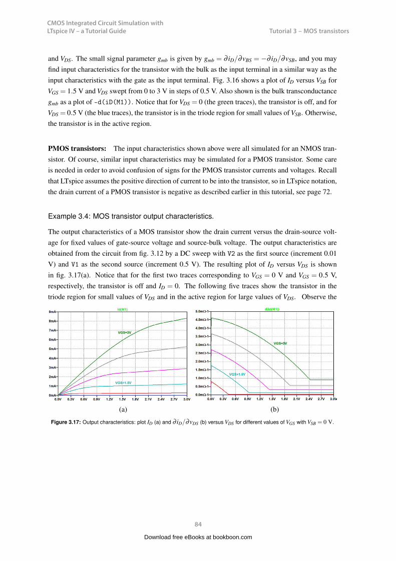
CMOS Integrated Circuit Simulation with LTspice IV – a Tutorial Guide
84
Tutorial 3 – MOS transistorsCMOS Integrated Circuit Simulation with LTspice IV Tutorial 3
and VDS. The small signal parameter gmb is given by gmb = ∂ iD/∂vBS = −∂ iD/∂vSB, and you mayfind input characteristics for the transistor with the bulk as the input terminal in a similar way as theinput characteristics with the gate as the input terminal. Fig. 3.16 shows a plot of ID versus VSB forVGS = 1.5 V and VDS swept from 0 to 3 V in steps of 0.5 V. Also shown is the bulk transconductancegmb as a plot of -d(iD(M1)). Notice that for VDS = 0 (the green traces), the transistor is off, and forVDS = 0.5 V (the blue traces), the transistor is in the triode region for small values of VSB. Otherwise,the transistor is in the active region.
PMOS transistors: The input characteristics shown above were all simulated for an NMOS tran-sistor. Of course, similar input characteristics may be simulated for a PMOS transistor. Some careis needed in order to avoid confusion of signs for the PMOS transistor currents and voltages. Recallthat LTspice assumes the positive direction of current to be into the transistor, so in LTspice notation,the drain current of a PMOS transistor is negative as described earlier in this tutorial, see page 72.
Example 3.4: MOS transistor output characteristics.
The output characteristics of a MOS transistor show the drain current versus the drain-source volt-age for fixed values of gate-source voltage and source-bulk voltage. The output characteristics areobtained from the circuit from fig. 3.12 by a DC sweep with V2 as the first source (increment 0.01V) and V1 as the second source (increment 0.5 V). The resulting plot of ID versus VDS is shownin fig. 3.17(a). Notice that for the first two traces corresponding to VGS = 0 V and VGS = 0.5 V,respectively, the transistor is off and ID = 0. The following five traces show the transistor in thetriode region for small values of VDS and in the active region for large values of VDS. Observe the
(a) (b)
Figure 3.17: Output characteristics: plot ID (a) and ∂ iD/∂vDS (b) versus VDS for different values of VGS with VSB = 0 V.
84
Download free eBooks at bookboon.com
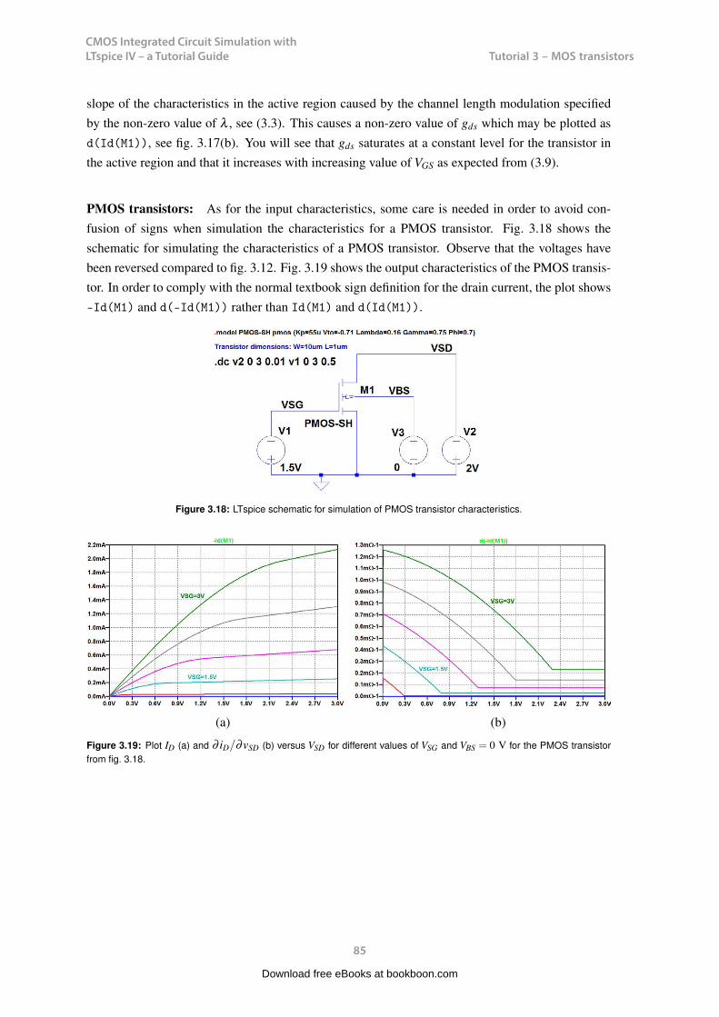
CMOS Integrated Circuit Simulation with LTspice IV – a Tutorial Guide
85
Tutorial 3 – MOS transistorsCMOS Integrated Circuit Simulation with LTspice IV Tutorial 3
slope of the characteristics in the active region caused by the channel length modulation specifiedby the non-zero value of λ , see (3.3). This causes a non-zero value of gds which may be plotted asd(Id(M1)), see fig. 3.17(b). You will see that gds saturates at a constant level for the transistor inthe active region and that it increases with increasing value of VGS as expected from (3.9).
PMOS transistors: As for the input characteristics, some care is needed in order to avoid con-fusion of signs when simulation the characteristics for a PMOS transistor. Fig. 3.18 shows theschematic for simulating the characteristics of a PMOS transistor. Observe that the voltages havebeen reversed compared to fig. 3.12. Fig. 3.19 shows the output characteristics of the PMOS transis-tor. In order to comply with the normal textbook sign definition for the drain current, the plot shows-Id(M1) and d(-Id(M1)) rather than Id(M1) and d(Id(M1)).
Figure 3.18: LTspice schematic for simulation of PMOS transistor characteristics.
(a) (b)
Figure 3.19: Plot ID (a) and ∂ iD/∂vSD (b) versus VSD for different values of VSG and VBS = 0 V for the PMOS transistorfrom fig. 3.18.
85
Download free eBooks at bookboon.com
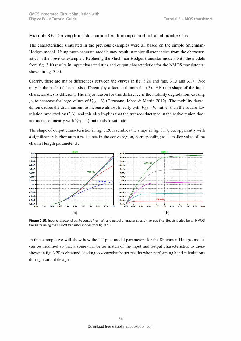
CMOS Integrated Circuit Simulation with LTspice IV – a Tutorial Guide
86
Tutorial 3 – MOS transistorsCMOS Integrated Circuit Simulation with LTspice IV Tutorial 3
Example 3.5: Deriving transistor parameters from input and output characteristics.
The characteristics simulated in the previous examples were all based on the simple Shichman-Hodges model. Using more accurate models may result in major discrepancies from the character-istics in the previous examples. Replacing the Shichman-Hodges transistor models with the modelsfrom fig. 3.10 results in input characteristics and output characteristics for the NMOS transistor asshown in fig. 3.20.
Clearly, there are major differences between the curves in fig. 3.20 and figs. 3.13 and 3.17. Notonly is the scale of the y-axis different (by a factor of more than 3). Also the shape of the inputcharacteristics is different. The major reason for this difference is the mobility degradation, causingµn to decrease for large values of VGS −Vt (Carusone, Johns & Martin 2012). The mobility degra-dation causes the drain current to increase almost linearly with VGS −Vt , rather than the square-lawrelation predicted by (3.3), and this also implies that the transconductance in the active region doesnot increase linearly with VGS −Vt but tends to saturate.
The shape of output characteristics in fig. 3.20 resembles the shape in fig. 3.17, but apparently witha significantly higher output resistance in the active region, corresponding to a smaller value of thechannel length parameter λ .
(a) (b)
Figure 3.20: Input characteristics, ID versus VGS, (a), and output characteristics, ID versus VDS, (b), simulated for an NMOStransistor using the BSIM3 transistor model from fig. 3.10.
In this example we will show how the LTspice model parameters for the Shichman-Hodges modelcan be modified so that a somewhat better match of the input and output characteristics to thoseshown in fig. 3.20 is obtained, leading to somewhat better results when performing hand calculationsduring a circuit design.
We will use a simple, heuristic approach. More advanced methods (e.g. using linear regression
86
Download free eBooks at bookboon.com

CMOS Integrated Circuit Simulation with LTspice IV – a Tutorial Guide
87
Tutorial 3 – MOS transistorsCMOS Integrated Circuit Simulation with LTspice IV Tutorial 3
Figure 3.21: LTspice schematic for simulation of transistor characteristics for two different transistor models.
techniques) can be found in the literature, e.g. (Allen & Holberg 2012, Appendix B), but with thelarge discrepancies which cannot be avoided, a few simple methods may be sufficient in many cases.
In order to be able to compare the simulation results for the Shichman-Hodges model and an ad-vanced model, it is useful to simulate the two models in parallel using the circuit configuration shownin fig. 3.21. This figure shows the circuit from fig. 3.12 augmented with an extra transistor M2 con-nected in parallel with M1 and specified with the model NMOS-BSIM from the library BSIM3_035.lib.This parallel connection is achieved without drawing wires between the two transistor. The labelsdefining the names of the nodes is enough to establish the correct connections in the LTspice netlist.
87
CMOS Integrated Circuit Simulation with LTspice IV Tutorial 3
Example 3.5: Deriving transistor parameters from input and output characteristics.
The characteristics simulated in the previous examples were all based on the simple Shichman-Hodges model. Using more accurate models may result in major discrepancies from the character-istics in the previous examples. Replacing the Shichman-Hodges transistor models with the modelsfrom fig. 3.10 results in input characteristics and output characteristics for the NMOS transistor asshown in fig. 3.20.
Clearly, there are major differences between the curves in fig. 3.20 and figs. 3.13 and 3.17. Notonly is the scale of the y-axis different (by a factor of more than 3). Also the shape of the inputcharacteristics is different. The major reason for this difference is the mobility degradation, causingµn to decrease for large values of VGS −Vt (Carusone, Johns & Martin 2012). The mobility degra-dation causes the drain current to increase almost linearly with VGS −Vt , rather than the square-lawrelation predicted by (3.3), and this also implies that the transconductance in the active region doesnot increase linearly with VGS −Vt but tends to saturate.
The shape of output characteristics in fig. 3.20 resembles the shape in fig. 3.17, but apparently witha significantly higher output resistance in the active region, corresponding to a smaller value of thechannel length parameter λ .
(a) (b)
Figure 3.20: Input characteristics, ID versus VGS, (a), and output characteristics, ID versus VDS, (b), simulated for an NMOStransistor using the BSIM3 transistor model from fig. 3.10.
In this example we will show how the LTspice model parameters for the Shichman-Hodges modelcan be modified so that a somewhat better match of the input and output characteristics to thoseshown in fig. 3.20 is obtained, leading to somewhat better results when performing hand calculationsduring a circuit design.
We will use a simple, heuristic approach. More advanced methods (e.g. using linear regression
86
CMOS Integrated Circuit Simulation with LTspice IV Tutorial 3
Figure 3.21: LTspice schematic for simulation of transistor characteristics for two different transistor models.
techniques) can be found in the literature, e.g. (Allen & Holberg 2012, Appendix B), but with thelarge discrepancies which cannot be avoided, a few simple methods may be sufficient in many cases.
In order to be able to compare the simulation results for the Shichman-Hodges model and an ad-vanced model, it is useful to simulate the two models in parallel using the circuit configuration shownin fig. 3.21. This figure shows the circuit from fig. 3.12 augmented with an extra transistor M2 con-nected in parallel with M1 and specified with the model NMOS-BSIM from the library BSIM3_035.lib.This parallel connection is achieved without drawing wires between the two transistor. The labelsdefining the names of the nodes is enough to establish the correct connections in the LTspice netlist.
87
Download free eBooks at bookboon.com
Click on the ad to read moreClick on the ad to read moreClick on the ad to read moreClick on the ad to read moreClick on the ad to read moreClick on the ad to read moreClick on the ad to read moreClick on the ad to read moreClick on the ad to read moreClick on the ad to read moreClick on the ad to read moreClick on the ad to read moreClick on the ad to read moreClick on the ad to read moreClick on the ad to read moreClick on the ad to read moreClick on the ad to read moreClick on the ad to read moreClick on the ad to read moreClick on the ad to read moreClick on the ad to read moreClick on the ad to read moreClick on the ad to read moreClick on the ad to read moreClick on the ad to read moreClick on the ad to read moreClick on the ad to read moreClick on the ad to read moreClick on the ad to read more
“The perfect start of a successful, international career.”
CLICK HERE to discover why both socially
and academically the University
of Groningen is one of the best
places for a student to be www.rug.nl/feb/education
Excellent Economics and Business programmes at:
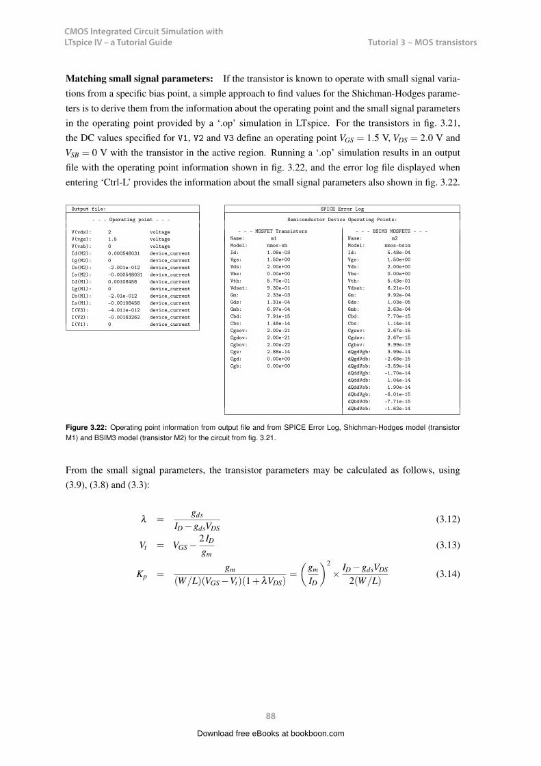
CMOS Integrated Circuit Simulation with LTspice IV – a Tutorial Guide
88
Tutorial 3 – MOS transistorsCMOS Integrated Circuit Simulation with LTspice IV Tutorial 3
Matching small signal parameters: If the transistor is known to operate with small signal varia-tions from a specific bias point, a simple approach to find values for the Shichman-Hodges parame-ters is to derive them from the information about the operating point and the small signal parametersin the operating point provided by a ‘.op’ simulation in LTspice. For the transistors in fig. 3.21,the DC values specified for V1, V2 and V3 define an operating point VGS = 1.5 V, VDS = 2.0 V andVSB = 0 V with the transistor in the active region. Running a ‘.op’ simulation results in an outputfile with the operating point information shown in fig. 3.22, and the error log file displayed whenentering ‘Ctrl-L’ provides the information about the small signal parameters also shown in fig. 3.22.
Output file:
- - - Operating point - - -
V(vds): 2 voltageV(vgs): 1.5 voltageV(vsb): 0 voltageId(M2): 0.000548031 device_currentIg(M2): 0 device_currentIb(M2): -2.001e-012 device_currentIs(M2): -0.000548031 device_currentId(M1): 0.00108458 device_currentIg(M1): 0 device_currentIb(M1): -2.01e-012 device_currentIs(M1): -0.00108458 device_currentI(V3): -4.011e-012 device_currentI(V2): -0.00163262 device_currentI(V1): 0 device_current
SPICE Error Log
Semiconductor Device Operating Points:
- - - MOSFET Transistors - - - BSIM3 MOSFETS - - -Name: m1 Name: m2Model: nmos-sh Model: nmos-bsimId: 1.08e-03 Id: 5.48e-04Vgs: 1.50e+00 Vgs: 1.50e+00Vds: 2.00e+00 Vds: 2.00e+00Vbs: 0.00e+00 Vbs: 0.00e+00Vth: 5.70e-01 Vth: 5.43e-01Vdsat: 9.30e-01 Vdsat: 6.21e-01Gm: 2.33e-03 Gm: 9.92e-04Gds: 1.31e-04 Gds: 1.03e-05Gmb: 6.97e-04 Gmb: 2.63e-04Cbd: 7.91e-15 Cbd: 7.70e-15Cbs: 1.48e-14 Cbs: 1.14e-14Cgsov: 2.00e-21 Cgsov: 2.67e-15Cgdov: 2.00e-21 Cgdov: 2.67e-15Cgbov: 2.00e-22 Cgbov: 9.99e-19Cgs: 2.88e-14 dQgdVgb: 3.99e-14Cgd: 0.00e+00 dQgdVdb: -2.68e-15Cgb: 0.00e+00 dQgdVsb: -3.59e-14
dQddVgb: -1.70e-14dQddVdb: 1.04e-14dQddVsb: 1.90e-14dQbdVgb: -6.01e-15dQbdVdb: -7.71e-15dQbdVsb: -1.62e-14
Figure 3.22: Operating point information from output file and from SPICE Error Log, Shichman-Hodges model (transistorM1) and BSIM3 model (transistor M2) for the circuit from fig. 3.21.
From the small signal parameters, the transistor parameters may be calculated as follows, using(3.9), (3.8) and (3.3):
λ =gds
ID −gdsVDS(3.12)
Vt = VGS −2 ID
gm(3.13)
Kp =gm
(W/L)(VGS −Vt)(1+λVDS)=
(gm
ID
)2
× ID −gdsVDS
2(W/L)(3.14)
88
Download free eBooks at bookboon.com

CMOS Integrated Circuit Simulation with LTspice IV – a Tutorial Guide
89
Tutorial 3 – MOS transistorsCMOS Integrated Circuit Simulation with LTspice IV Tutorial 3
Assuming a value of 0.7 V for |2ΦF |, the bulk effect parameter γ may be calculated using (3.10)with VSB = 0:
γ = 2√
|2ΦF |×gmb
gm= 1.67× gmb
gm(3.15)
For the simulation results from fig. 3.22, this results in λ = 0.0195 V−1, Vt = 0.395 V, Kp = 86.4µA/V2 and γ = 0.44
√V.
With these model parameters inserted for the model NMOS-SH, the ‘.op’ analysis gives the operat-ing point information shown in fig. 3.23. Obviously, there is a close match between the bias pointinformation and small signal parameters for M1 and M2.
While the transistor parameters have been adjusted to match in the bias point, this does not nec-essarily ensures a good match over a range of variations. This is illustrated in fig. 3.24, showingsimulated input characteristics and output characteristics for both transistors in the same plot. Forsimplicity, the input characteristics are shown only for VDS = 1.5 V, 2.0 V and 2.5 V, and the out-put characteristics are shown only for VGS = 1.0 V, 1.5 V, 2.0 V and 2.5 V. Evidently, the matchbetween the two transistors is reasonable for variations around the bias point but is less good whenthe transistors operate in the triode region and for large values of VGS and VDS where the mobilitydegradation is important.
89
Download free eBooks at bookboon.com
Click on the ad to read moreClick on the ad to read moreClick on the ad to read moreClick on the ad to read moreClick on the ad to read moreClick on the ad to read moreClick on the ad to read moreClick on the ad to read moreClick on the ad to read moreClick on the ad to read moreClick on the ad to read moreClick on the ad to read moreClick on the ad to read moreClick on the ad to read moreClick on the ad to read moreClick on the ad to read moreClick on the ad to read moreClick on the ad to read moreClick on the ad to read moreClick on the ad to read moreClick on the ad to read moreClick on the ad to read moreClick on the ad to read moreClick on the ad to read moreClick on the ad to read moreClick on the ad to read moreClick on the ad to read moreClick on the ad to read moreClick on the ad to read moreClick on the ad to read more
89,000 kmIn the past four years we have drilled
That’s more than twice around the world.
careers.slb.com
What will you be?
1 Based on Fortune 500 ranking 2011. Copyright © 2015 Schlumberger. All rights reserved.
Who are we?We are the world’s largest oilfield services company1. Working globally—often in remote and challenging locations— we invent, design, engineer, and apply technology to help our customers find and produce oil and gas safely.
Who are we looking for?Every year, we need thousands of graduates to begin dynamic careers in the following domains:n Engineering, Research and Operationsn Geoscience and Petrotechnicaln Commercial and Business
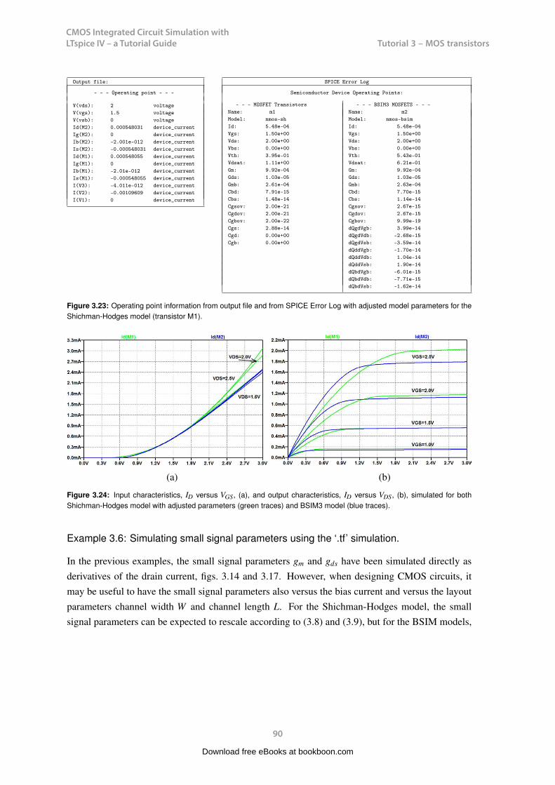
CMOS Integrated Circuit Simulation with LTspice IV – a Tutorial Guide
90
Tutorial 3 – MOS transistorsCMOS Integrated Circuit Simulation with LTspice IV Tutorial 3
Output file:
- - - Operating point - - -
V(vds): 2 voltageV(vgs): 1.5 voltageV(vsb): 0 voltageId(M2): 0.000548031 device_currentIg(M2): 0 device_currentIb(M2): -2.001e-012 device_currentIs(M2): -0.000548031 device_currentId(M1): 0.000548055 device_currentIg(M1): 0 device_currentIb(M1): -2.01e-012 device_currentIs(M1): -0.000548055 device_currentI(V3): -4.011e-012 device_currentI(V2): -0.00109609 device_currentI(V1): 0 device_current
SPICE Error Log
Semiconductor Device Operating Points:
- - - MOSFET Transistors - - - BSIM3 MOSFETS - - -Name: m1 Name: m2Model: nmos-sh Model: nmos-bsimId: 5.48e-04 Id: 5.48e-04Vgs: 1.50e+00 Vgs: 1.50e+00Vds: 2.00e+00 Vds: 2.00e+00Vbs: 0.00e+00 Vbs: 0.00e+00Vth: 3.95e-01 Vth: 5.43e-01Vdsat: 1.11e+00 Vdsat: 6.21e-01Gm: 9.92e-04 Gm: 9.92e-04Gds: 1.03e-05 Gds: 1.03e-05Gmb: 2.61e-04 Gmb: 2.63e-04Cbd: 7.91e-15 Cbd: 7.70e-15Cbs: 1.48e-14 Cbs: 1.14e-14Cgsov: 2.00e-21 Cgsov: 2.67e-15Cgdov: 2.00e-21 Cgdov: 2.67e-15Cgbov: 2.00e-22 Cgbov: 9.99e-19Cgs: 2.88e-14 dQgdVgb: 3.99e-14Cgd: 0.00e+00 dQgdVdb: -2.68e-15Cgb: 0.00e+00 dQgdVsb: -3.59e-14
dQddVgb: -1.70e-14dQddVdb: 1.04e-14dQddVsb: 1.90e-14dQbdVgb: -6.01e-15dQbdVdb: -7.71e-15dQbdVsb: -1.62e-14
Figure 3.23: Operating point information from output file and from SPICE Error Log with adjusted model parameters for theShichman-Hodges model (transistor M1).
(a) (b)
Figure 3.24: Input characteristics, ID versus VGS, (a), and output characteristics, ID versus VDS, (b), simulated for bothShichman-Hodges model with adjusted parameters (green traces) and BSIM3 model (blue traces).
Example 3.6: Simulating small signal parameters using the ‘.tf’ simulation.
In the previous examples, the small signal parameters gm and gds have been simulated directly asderivatives of the drain current, figs. 3.14 and 3.17. However, when designing CMOS circuits, itmay be useful to have the small signal parameters also versus the bias current and versus the layoutparameters channel width W and channel length L. For the Shichman-Hodges model, the smallsignal parameters can be expected to rescale according to (3.8) and (3.9), but for the BSIM models,
90
Download free eBooks at bookboon.com
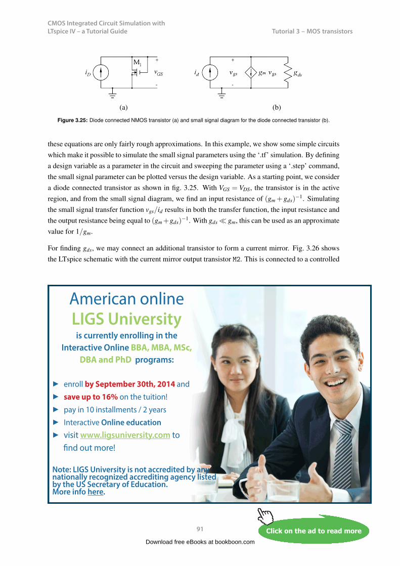
CMOS Integrated Circuit Simulation with LTspice IV – a Tutorial Guide
91
Tutorial 3 – MOS transistorsCMOS Integrated Circuit Simulation with LTspice IV Tutorial 3
(a) (b)
Figure 3.25: Diode connected NMOS transistor (a) and small signal diagram for the diode connected transistor (b).
these equations are only fairly rough approximations. In this example, we show some simple circuitswhich make it possible to simulate the small signal parameters using the ‘.tf’ simulation. By defininga design variable as a parameter in the circuit and sweeping the parameter using a ‘.step’ command,the small signal parameter can be plotted versus the design variable. As a starting point, we considera diode connected transistor as shown in fig. 3.25. With VGS = VDS, the transistor is in the activeregion, and from the small signal diagram, we find an input resistance of (gm +gds)
−1. Simulatingthe small signal transfer function vgs/id results in both the transfer function, the input resistance andthe output resistance being equal to (gm+gds)
−1. With gds gm, this can be used as an approximatevalue for 1/gm.
For finding gds, we may connect an additional transistor to form a current mirror. Fig. 3.26 showsthe LTspice schematic with the current mirror output transistor M2. This is connected to a controlled
91
Download free eBooks at bookboon.com
Click on the ad to read moreClick on the ad to read moreClick on the ad to read moreClick on the ad to read moreClick on the ad to read moreClick on the ad to read moreClick on the ad to read moreClick on the ad to read moreClick on the ad to read moreClick on the ad to read moreClick on the ad to read moreClick on the ad to read moreClick on the ad to read moreClick on the ad to read moreClick on the ad to read moreClick on the ad to read moreClick on the ad to read moreClick on the ad to read moreClick on the ad to read moreClick on the ad to read moreClick on the ad to read moreClick on the ad to read moreClick on the ad to read moreClick on the ad to read moreClick on the ad to read moreClick on the ad to read moreClick on the ad to read moreClick on the ad to read moreClick on the ad to read moreClick on the ad to read moreClick on the ad to read more
American online LIGS University
enroll by September 30th, 2014 and
save up to 16% on the tuition!
pay in 10 installments / 2 years
Interactive Online education visit www.ligsuniversity.com to
find out more!
is currently enrolling in theInteractive Online BBA, MBA, MSc,
DBA and PhD programs:
Note: LIGS University is not accredited by any nationally recognized accrediting agency listed by the US Secretary of Education. More info here.
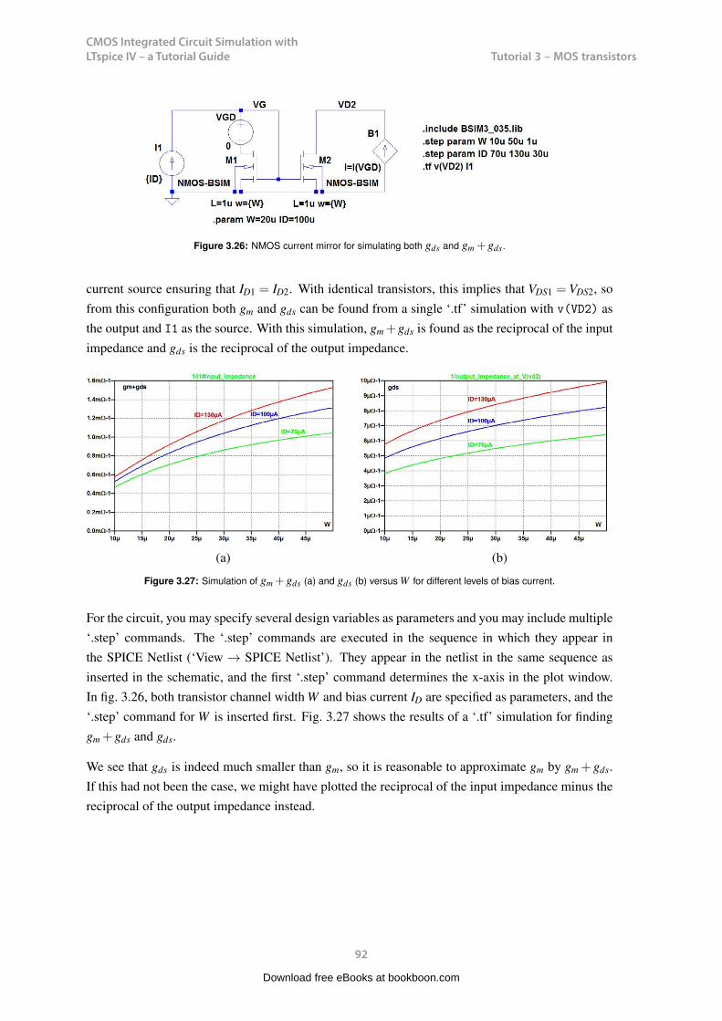
CMOS Integrated Circuit Simulation with LTspice IV – a Tutorial Guide
92
Tutorial 3 – MOS transistorsCMOS Integrated Circuit Simulation with LTspice IV Tutorial 3
Figure 3.26: NMOS current mirror for simulating both gds and gm +gds.
current source ensuring that ID1 = ID2. With identical transistors, this implies that VDS1 = VDS2, sofrom this configuration both gm and gds can be found from a single ‘.tf’ simulation with v(VD2) asthe output and I1 as the source. With this simulation, gm+gds is found as the reciprocal of the inputimpedance and gds is the reciprocal of the output impedance.
(a) (b)
Figure 3.27: Simulation of gm +gds (a) and gds (b) versus W for different levels of bias current.
For the circuit, you may specify several design variables as parameters and you may include multiple‘.step’ commands. The ‘.step’ commands are executed in the sequence in which they appear inthe SPICE Netlist (‘View → SPICE Netlist’). They appear in the netlist in the same sequence asinserted in the schematic, and the first ‘.step’ command determines the x-axis in the plot window.In fig. 3.26, both transistor channel width W and bias current ID are specified as parameters, and the‘.step’ command for W is inserted first. Fig. 3.27 shows the results of a ‘.tf’ simulation for findinggm +gds and gds.
We see that gds is indeed much smaller than gm, so it is reasonable to approximate gm by gm +gds.If this had not been the case, we might have plotted the reciprocal of the input impedance minus thereciprocal of the output impedance instead.
92
Download free eBooks at bookboon.com
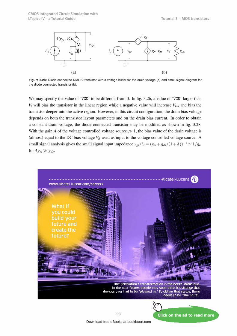
CMOS Integrated Circuit Simulation with LTspice IV – a Tutorial Guide
93
Tutorial 3 – MOS transistorsCMOS Integrated Circuit Simulation with LTspice IV Tutorial 3
(a) (b)
Figure 3.28: Diode connected NMOS transistor with a voltage buffer for the drain voltage (a) and small signal diagram forthe diode connected transistor (b).
We may specify the value of ‘VGD’ to be different from 0. In fig. 3.26, a value of ‘VGD’ larger thanVt will bias the transistor in the linear region while a negative value will increase VDS and bias thetransistor deeper into the active region. However, in this circuit configuration, the drain bias voltagedepends on both the transistor layout parameters and on the drain bias current. In order to obtaina constant drain voltage, the diode connected transistor may be modified as shown in fig. 3.28.With the gain A of the voltage controlled voltage source 1, the bias value of the drain voltage is(almost) equal to the DC bias voltage VB used as input to the voltage controlled voltage source. Asmall signal analysis gives the small signal input impedance vgs/id = (gm +gds/(1+A))−1 1/gm
for Agm gds.
93
Download free eBooks at bookboon.com
Click on the ad to read moreClick on the ad to read moreClick on the ad to read moreClick on the ad to read moreClick on the ad to read moreClick on the ad to read moreClick on the ad to read moreClick on the ad to read moreClick on the ad to read moreClick on the ad to read moreClick on the ad to read moreClick on the ad to read moreClick on the ad to read moreClick on the ad to read moreClick on the ad to read moreClick on the ad to read moreClick on the ad to read moreClick on the ad to read moreClick on the ad to read moreClick on the ad to read moreClick on the ad to read moreClick on the ad to read moreClick on the ad to read moreClick on the ad to read moreClick on the ad to read moreClick on the ad to read moreClick on the ad to read moreClick on the ad to read moreClick on the ad to read moreClick on the ad to read moreClick on the ad to read moreClick on the ad to read more
.
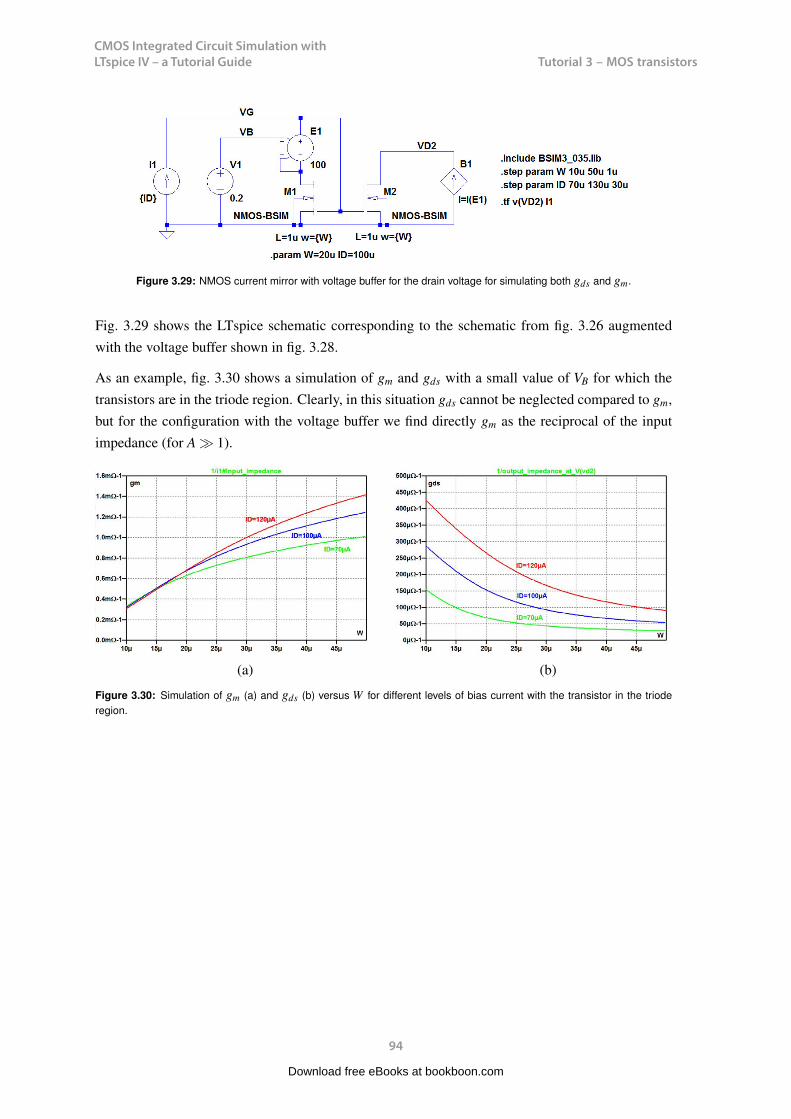
CMOS Integrated Circuit Simulation with LTspice IV – a Tutorial Guide
94
Tutorial 3 – MOS transistorsCMOS Integrated Circuit Simulation with LTspice IV Tutorial 3
Figure 3.29: NMOS current mirror with voltage buffer for the drain voltage for simulating both gds and gm.
Fig. 3.29 shows the LTspice schematic corresponding to the schematic from fig. 3.26 augmentedwith the voltage buffer shown in fig. 3.28.
As an example, fig. 3.30 shows a simulation of gm and gds with a small value of VB for which thetransistors are in the triode region. Clearly, in this situation gds cannot be neglected compared to gm,but for the configuration with the voltage buffer we find directly gm as the reciprocal of the inputimpedance (for A 1).
(a) (b)
Figure 3.30: Simulation of gm (a) and gds (b) versus W for different levels of bias current with the transistor in the trioderegion.
94
Download free eBooks at bookboon.com
CMOS Integrated Circuit Simulation with LTspice IV – a Tutorial Guide
95
Tutorial 3 – MOS transistorsCMOS Integrated Circuit Simulation with LTspice IV Tutorial 3
Hints and pitfalls
– LTspice defines the positive direction of current flow into the transistor, so the drain currentin a PMOS transistor is normally negative (or zero).
– The output file from an operating point simulation (‘.op’) provides information about nodevoltages and device currents.
– The SPICE Error Log (hotkey ‘Ctrl-L’) from an operating point simulation (‘.op’) providesinformation about bias points and small signal parameters for the transistors in a circuit.
– Simple transistor models may be entered directly in the schematic using a ‘.model’ SPICEDirective. Advanced transistor models are included using model files and a ‘.include’SPICE Directive.
– A model file can be opened and viewed in LTspice using the command ‘Files → Open’ andspecifying ‘Files of type → All Files’.
– The default model names for ‘nmos4’ and ‘pmos4’ transistors are NMOS and PMOS. Ifyour ‘.model’ directives or model file use model names different from this, remember tochange the model name when specifying the transistor parameters for each transistor (seefig. 3.1 on page 68). Otherwise, the simulation will run with a default Shichman-Hodgestransistor model with ‘Kp=2e-5’, ‘Vto=0’, ‘Lambda=0’, ‘Gamma=0’, and ‘Phi=0.6’.
– Remember to re-calculate the channel length modulation parameter ‘Lambda’ in theShichman-Hodges transistor model when changing the channel length of a transistor. Itis inversely proportional to the channel length.
– When using the Shichman-Hodges model, separate transistor models are required for tran-sistors with different channel lengths in order to specify different values for ‘Lambda’.
– When having multiple traces in a simulation plot (e.g. output characteristics for differentvalues of VGS), one or two cursors may be attached to the traces and moved from one traceto another by the up-arrow key and the down-arrow key.
– The information about a trace followed by a cursor is displayed by right clicking on thecursor number.
– When using two ‘.step’ commands in a schematic, the x-axis in the simulation plot isdetermined by the ‘.step’ command appearing first in the netlist. This is the commandinserted first in the schematic.
– Text (comments) can be placed in a schematic using the command ‘Edit → Text’, toolbarsymbol or hotkey ‘T’.
– Text and other annotations, (e.g. cursor position) can be placed in a simulation plot usingthe command ‘Plot Settings → Notes & Annotations’.
95
Download free eBooks at bookboon.com

CMOS Integrated Circuit Simulation with LTspice IV – a Tutorial Guide
96
Tutorial 3 – MOS transistorsCMOS Integrated Circuit Simulation with LTspice IV Tutorial 3
References
Allen, PE., & Holberg, DR. 2012, CMOS Analog Integrated Circuit Design, Third Edition, OxfordUniversity Press, New York, USA.
Baker, RJ. 2010, CMOS Circuit Design, Layout, and Simulation, Third Edition, IEEE Press, Piscat-away, USA.
Carusone, TC., Johns, D. & Martin, K. 2012, Analog Integrated Circuit Design, Second Edition,John Wiley & Sons, Inc., Hoboken, USA.
Carusone, TC., Johns, D. & Martin, K. 2014, Analog Integrated Circuit Design, Netlist and modelfiles. Retrieved from http://analogicdesign.com/students/netlists-models/
Enz, CC. & Vittoz, EA. 2006, Charge-Based MOS Transistor Modeling: The EKV Model for Low-Power and RF Design, John Wiley & Sons, Ltd., Chichester, UK.
Sedra, AS. & Smith, KC. 2011, Microelectronic Circuits, International Sixth Edition, Oxford Uni-versity Press, New York, USA.
Sheu, BJ., Sharfetter, DL., Ko, P-K. & Jeng, M-C. 1987, ‘BSIM: Berkeley Short-Channel IGFETModel for MOS Transistors’, IEEE J. Solid-State Circuit, vol. SC-22, No. 4, pp. 558-566.
96
Download free eBooks at bookboon.com
Click on the ad to read moreClick on the ad to read moreClick on the ad to read moreClick on the ad to read moreClick on the ad to read moreClick on the ad to read moreClick on the ad to read moreClick on the ad to read moreClick on the ad to read moreClick on the ad to read moreClick on the ad to read moreClick on the ad to read moreClick on the ad to read moreClick on the ad to read moreClick on the ad to read moreClick on the ad to read moreClick on the ad to read moreClick on the ad to read moreClick on the ad to read moreClick on the ad to read moreClick on the ad to read moreClick on the ad to read moreClick on the ad to read moreClick on the ad to read moreClick on the ad to read moreClick on the ad to read moreClick on the ad to read moreClick on the ad to read moreClick on the ad to read moreClick on the ad to read moreClick on the ad to read moreClick on the ad to read moreClick on the ad to read more
www.mastersopenday.nl
Visit us and find out why we are the best!Master’s Open Day: 22 February 2014
Join the best atthe Maastricht UniversitySchool of Business andEconomics!
Top master’s programmes• 33rdplaceFinancialTimesworldwideranking:MScInternationalBusiness
• 1stplace:MScInternationalBusiness• 1stplace:MScFinancialEconomics• 2ndplace:MScManagementofLearning• 2ndplace:MScEconomics• 2ndplace:MScEconometricsandOperationsResearch• 2ndplace:MScGlobalSupplyChainManagementandChange
Sources: Keuzegids Master ranking 2013; Elsevier ‘Beste Studies’ ranking 2012; Financial Times Global Masters in Management ranking 2012
MaastrichtUniversity is
the best specialistuniversity in the
Netherlands(Elsevier)

CMOS Integrated Circuit Simulation with LTspice IV – a Tutorial Guide
97
Tutorial 3 – MOS transistorsCMOS Integrated Circuit Simulation with LTspice IV Tutorial 3
Shichman, H. & Hodges, DA. 1968, ‘Modeling and Simulation of Insulated-Gate Field-Effect Tran-sistor Switching Circuits’, IEEE J. Solid-State Circuit, vol. SC-3, No. 3, pp. 285-289.
The MOSIS Service 2014. Retrieved from http://www.mosis.com/
The MOSIS Service: Wafer Electrical Test Data and SPICE Model Parameters 2014. Retrievedfrom https://www.mosis.com/pages/Technical/Testdata/tsmc-035-prm
Tsividis, Y. & McAndrew, C. 2010, Operation and Modeling of the MOS Transistor, Third Edition,Oxford University Press, New York, USA.
97
Download free eBooks at bookboon.com
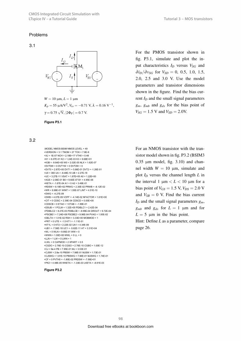
CMOS Integrated Circuit Simulation with LTspice IV – a Tutorial Guide
98
Tutorial 3 – MOS transistorsCMOS Integrated Circuit Simulation with LTspice IV Tutorial 3
Problems
3.1
W = 10 µm, L = 1 µm
Kp = 55 µA/V2, Vto =−0.71 V, λ = 0.16 V−1,
γ = 0.75√
V, |2ΦF |= 0.7 V.
Figure P3.1
For the PMOS transistor shown infig. P3.1, simulate and plot the in-put characteristics ID versus VSG and∂ iD/∂vSG for VSD = 0, 0.5, 1.0, 1.5,2.0, 2.5 and 3.0 V. Use the modelparameters and transistor dimensionsshown in the figure. Find the bias cur-rent ID and the small signal parametersgm, gmb and gds for the bias point ofVSG = 1.5 V and VSD = 2.0V.
3.2
.MODEL NMOS-BSIM NMOS LEVEL = 49+VERSION = 3.1 TNOM = 27 TOX = 7.8E-9 +XJ = 1E-07 NCH = 2.18E+17 VTH0 = 0.48+K1 = 6.07E-01 K2 = 1.24E-03 K3 = 9.68E+01+K3B = -9.84E+00 W0 = 2.02E-05 NLX = 1.62E-07+DVT0W = 0 DVT1W = 0 DVT2W = 0+DVT0 = 2.87E+00 DVT1 = 5.86E-01 DVT2 = -1.26E-01+U0 = 360 UA = -8.48E-10 UB = 2.27E-18+UC = 3.27E-11 VSAT = 1.87E+05 A0 = 1.22E+00+AGS = 2.06E-01 B0 = 9.60E-07 B1 = 4.95E-06+KETA = -1.67E-04 A1 = 0 A2 = 3.49E-01+RDSW = 8.18E+02 PRWG = 2.35E-02 PRWB = -8.12E-02+WR = 9.98E-01 WINT = 1.55E-07 LINT = 4.51E-10+DWG = -4.27E-09+DWB = 4.07E-09 VOFF = -4.14E-02 NFACTOR = 1.61E+00+CIT = 0 CDSC = 2.39E-04 CDSCD = 0.00E+00+CDSCB = 0 ETA0 = 1 ETAB = -1.99E-01+DSUB = 1 PCLM = 1.32E+00 PDIBLC1 = 2.42E-04+PDIBLC2 = 8.27E-03 PDIBLCB = -9.99E-04 DROUT = 9.72E-04+PSCBE1 = 7.24E+08 PSCBE2 = 9.96E-04 PVAG = 1.00E-02+DELTA = 1.01E-02 RSH = 3.33E+00 MOBMOD = 1+PRT = 0 UTE = -1.5 KT1 = -1.11E-01+KT1L = 0 KT2 = 2.22E-02 UA1 = 4.34E-09+UB1 = -7.56E-18 UC1 = -5.62E-11 AT = 3.31E+04+WL = 0 WLN = 9.95E-01 WW = 0+WWN = 1.00E+00 WWL = 0 LL = 0+LLN = 1 LW = 0 LWN = 1+LWL = 0 CAPMOD = 2 XPART = 0.5+CGDO = 2.76E-10 CGSO = 2.76E-10 CGBO = 1.00E-12+CJ = 9e-4 PB = 7.95E-01 MJ = 3.53E-01+CJSW = 2.8e-10 PBSW = 7.98E-01 MJSW = 1.73E-01+CJSWG = 1.81E-10 PBSWG = 7.96E-01 MJSWG = 1.74E-01+CF = 0 PVTH0 = -1.80E-02 PRDSW = -7.56E+01+PK2 = 4.48E-05 WKETA = -1.33E-03 LKETA = -8.91E-03
Figure P3.2
For an NMOS transistor with the tran-sistor model shown in fig. P3.2 (BSIM30.35 µm model, fig. 3.10) and chan-nel width W = 10 µm, simulate andplot ID versus the channel length L inthe interval 1 µm < L < 10 µm for abias point of VGS = 1.5 V, VDS = 2.0 Vand VSB = 0 V. Find the bias currentID and the small signal parameters gm,gmb and gds for L = 1 µm and forL = 5 µm in the bias point.Hint: Define L as a parameter, comparepage 26.
98
Download free eBooks at bookboon.com

CMOS Integrated Circuit Simulation with LTspice IV – a Tutorial Guide
99
Tutorial 3 – MOS transistorsCMOS Integrated Circuit Simulation with LTspice IV Tutorial 3
3.3
.MODEL PMOS-BSIM PMOS LEVEL = 49+VERSION = 3.1 TNOM = 2.69E+01 TOX = 7.8E-9 +XJ = 1.00E-07 NCH = 8.44E+16 VTH0 = -0.6+K1 = 4.82E-01 K2 = -2.13E-02 K3 = 8.27E+01+K3B = -5 W0 = 5.24E-06 NLX = 2.49E-07+DVT0W = 0.00E+00 DVT1W = 0 DVT2W = 0+DVT0 = 3.54E-01 DVT1 = 7.52E-01 DVT2 = -2.98E-01+U0 = 150 UA = 1E-10 UB = 1.75E-18+UC = -2.27E-11 VSAT = 2.01E+05 A0 = 1.04E+00+AGS = 2.90E-01 B0 = 1.94E-06 B1 = 5.01E-06+KETA = -3.85E-03 A1 = 4.20E-03 A2 = 1.00E+00+RDSW = 4000 PRWG = -9.54E-02 PRWB = -1.92E-03+WR = 1 WINT = 1.47E-07 LINT = 1.04E-10+DWG = -1.09E-08+DWB = 1.14E-08 VOFF = -1.29E-01 NFACTOR = 2.01E+00+CIT = 0 CDSC = 2.40E-04 CDSCD = 0+CDSCB = 0 ETA0 = 4.07E-02 ETAB = 6.84E-03+DSUB = 3.21E-01 PCLM = 5.96E+00 PDIBLC1 = 2.89E-03+PDIBLC2 = -1.45E-06 PDIBLCB = -1E-03 DROUT = 9.93E-04+PSCBE1 = 7.88E+10 PSCBE2 = 5E-10 PVAG = 15+DELTA = 9.96E-03 RSH = 2.6 MOBMOD = 1+PRT = 0 UTE = -1.5 KT1 = -1.09E-01+KT1L = 0 KT2 = 2.19E-02 UA1 = 4.34E-09+UB1 = -7.62E-18 UC1 = -5.63E-11 AT = 3.28E+04+WL = 0 WLN = 1 WW = 0+WWN = 1.00E+00 WWL = 0 LL = 0+LLN = 1 LW = 0 LWN = 1+LWL = 0 CAPMOD = 2.01E+00 XPART = 0.5+CGDO = 2.10E-10 CGSO = 2.12E-10 CGBO = 1.00E-12+CJ = 14e-4 PB = 9.83E-01 MJ = 5.79E-01+CJSW = 3.2e-10 PBSW = 9.92E-01 MJSW = 3.60E-01+CJSWG = 4.41E-11 PBSWG = 9.85E-01 MJSWG = 3.58E-01+CF = 0 PVTH0 = 2.58E-02 PRDSW = -3.98E+01+PK2 = 2.02E-03 WKETA = 2.72E-03 LKETA = -7.14E-03
Figure P3.3
For a PMOS transistor with the transis-tor model shown in fig. P3.3 (BSIM30.35 µm model, fig. 3.10) and channelwidth W = 10 µm and channel lengthL = 1 µm, simulate and plot the inputcharacteristics ID versus VSG for VSD =
0, 0.5, 1.0, 1.5, 2.0, 2.5 and 3.0 V. As-sume VBS = 0 V. Also simulate and plotthe output characteristics ID versus VSD
for VSG = 0, 0.5, 1.0, 1.5, 2.0, 2.5 and3.0 V. Use the cursors to find ID and∂ iD/∂vSD for VSG = 1.5 V, VBS = 0 Vand VSD = 2.0 V.
99
Download free eBooks at bookboon.com
Click on the ad to read moreClick on the ad to read moreClick on the ad to read moreClick on the ad to read moreClick on the ad to read moreClick on the ad to read moreClick on the ad to read moreClick on the ad to read moreClick on the ad to read moreClick on the ad to read moreClick on the ad to read moreClick on the ad to read moreClick on the ad to read moreClick on the ad to read moreClick on the ad to read moreClick on the ad to read moreClick on the ad to read moreClick on the ad to read moreClick on the ad to read moreClick on the ad to read moreClick on the ad to read moreClick on the ad to read moreClick on the ad to read moreClick on the ad to read moreClick on the ad to read moreClick on the ad to read moreClick on the ad to read moreClick on the ad to read moreClick on the ad to read moreClick on the ad to read moreClick on the ad to read moreClick on the ad to read moreClick on the ad to read moreClick on the ad to read more
- ©
Pho
tono
nsto
p
> Apply now
redefine your future
AxA globAl grAduAte progrAm 2015
axa_ad_grad_prog_170x115.indd 1 19/12/13 16:36

CMOS Integrated Circuit Simulation with LTspice IV – a Tutorial Guide
100
Tutorial 3 – MOS transistorsCMOS Integrated Circuit Simulation with LTspice IV Tutorial 3
3.4For a PMOS transistor with the transis-tor model shown in fig. P3.3 (BSIM30.35 µm model, fig. 3.10) and channelwidth W = 10 µm and channel lengthL = 1 µm, find the bias current ID andthe small signal parameters gm, gmb
and gds in a bias point of VSG = 1.5 V,VBS = 0 V and VSD = 2.0 V. Fromthese small signal parameters and thebias current, estimate parameters for aShichman-Hodges model for the tran-sistor. Assume |2ΦF |= 0.7 V.Simulate and plot the input characteris-tics (ID versus VSG) and output charac-teristics (ID versus VSD).
100
Download free eBooks at bookboon.com
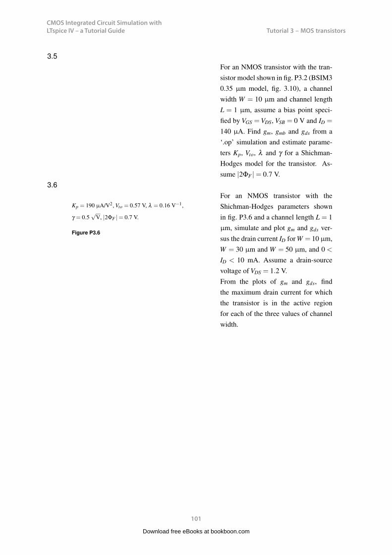
CMOS Integrated Circuit Simulation with LTspice IV – a Tutorial Guide
101
Tutorial 3 – MOS transistorsCMOS Integrated Circuit Simulation with LTspice IV Tutorial 3
3.5For an NMOS transistor with the tran-sistor model shown in fig. P3.2 (BSIM30.35 µm model, fig. 3.10), a channelwidth W = 10 µm and channel lengthL = 1 µm, assume a bias point speci-fied by VGS =VDS, VSB = 0 V and ID =
140 µA. Find gm, gmb and gds from a‘.op’ simulation and estimate parame-ters Kp, Vto, λ and γ for a Shichman-Hodges model for the transistor. As-sume |2ΦF |= 0.7 V.
3.6
Kp = 190 µA/V2, Vto = 0.57 V, λ = 0.16 V−1,
γ = 0.5√
V, |2ΦF |= 0.7 V.
Figure P3.6
For an NMOS transistor with theShichman-Hodges parameters shownin fig. P3.6 and a channel length L = 1µm, simulate and plot gm and gds ver-sus the drain current ID for W = 10 µm,W = 30 µm and W = 50 µm, and 0 <
ID < 10 mA. Assume a drain-sourcevoltage of VDS = 1.2 V.From the plots of gm and gds, findthe maximum drain current for whichthe transistor is in the active regionfor each of the three values of channelwidth.
101
Download free eBooks at bookboon.com

CMOS Integrated Circuit Simulation with LTspice IV – a Tutorial Guide
102
Tutorial 3 – MOS transistorsCMOS Integrated Circuit Simulation with LTspice IV Tutorial 3
Answers
3.1: ID = 227 µA; gm = 0.574 mA/V; gmb = 0.257 mA/V; gds = 27.5 µA/V
3.2: L = 1 µm: ID = 0.548 mA; gm = 0.992 mA/V; gmb = 0.263 mA/V; gds = 10.3 µA/V.L = 5 µm: ID = 0.127 mA; gm = 0.245 mA/V; gmb = 0.065 mA/V; gds = 1.94 µA/V.
3.3: ID = 0.16 mA; ∂ iD/∂vSD = 7.3 µA/V.
3.4: ID = 0.16 mA; gm = 0.339 mA/V; gmb = 0.0754 mA/V; gds = 7.31 µA/V;λ = 0.05 V−1; Vto =−0.557 V; Kp = 32.6 µA/V2; γ = 0.37
√V; |2ΦF |= 0.7 V.
3.5: gm = 0.584 mA/V; gmb = 0.167 mA/V; gds = 6.04 µA/V; λ = 0.045 V−1;Vto = 0.51 V; Kp = 117 µA/V2; γ = 0.48
√V; |2ΦF |= 0.7 V.
3.6: W = 10 µm: IDmax = 1.62 mA; W = 30 µm: IDmax = 4.89 mA; W = 50 µm: IDmax = 8.13 mA.
102
Download free eBooks at bookboon.com
Click on the ad to read moreClick on the ad to read moreClick on the ad to read moreClick on the ad to read moreClick on the ad to read moreClick on the ad to read moreClick on the ad to read moreClick on the ad to read moreClick on the ad to read moreClick on the ad to read moreClick on the ad to read moreClick on the ad to read moreClick on the ad to read moreClick on the ad to read moreClick on the ad to read moreClick on the ad to read moreClick on the ad to read moreClick on the ad to read moreClick on the ad to read moreClick on the ad to read moreClick on the ad to read moreClick on the ad to read moreClick on the ad to read moreClick on the ad to read moreClick on the ad to read moreClick on the ad to read moreClick on the ad to read moreClick on the ad to read moreClick on the ad to read moreClick on the ad to read moreClick on the ad to read moreClick on the ad to read moreClick on the ad to read moreClick on the ad to read moreClick on the ad to read more
CMOS Integrated Circuit Simulation with LTspice IV – a Tutorial Guide
103
Tutorial 4 – Basic gain stages
CMOS Integrated Circuit Simulation with LTspice IV Tutorial 4
Tutorial 4 – Basic gain stages
This tutorial introduces the basic CMOS gain stages and some of the issues arising when simulatingthe stages. The basic gain stages include the common source stage, the common drain stage, thecommon gate stage and the differential input pair. After having completed the tutorial, you shouldbe able to
– find bias currents and voltages for the standard configurations of basic gain stages.
– simulate the low frequency transfer function and the signal swings on the input and outputof a gain stage.
– find small signal parameters for the transistors in a gain stage.
– simulate the frequency response of a gain stage.
– perform design iterations from simple Shichman-Hodges transistor models to advancedSpice models.
– simulate common mode rejection ratio and power supply rejection ratio of a gain stage.
– simulate input impedances and output impedances of a gain stage.
– simulate the noise properties of a gain stage.
Example 4.1: The common source amplifier (inverting amplifier).
The simplest form of a common source stage is just an NMOS transistor with a resistor to provide thebias current as shown in fig. 4.1. This configuration is rarely used in integrated circuit design, but itprovides a good introduction to the common source stage and to steps in design iterations involvingdifferent transistor models. Hence, we will start by analyzing this configuration and subsequentlyexamine a common source configuration with an active load.
103
Download free eBooks at bookboon.com
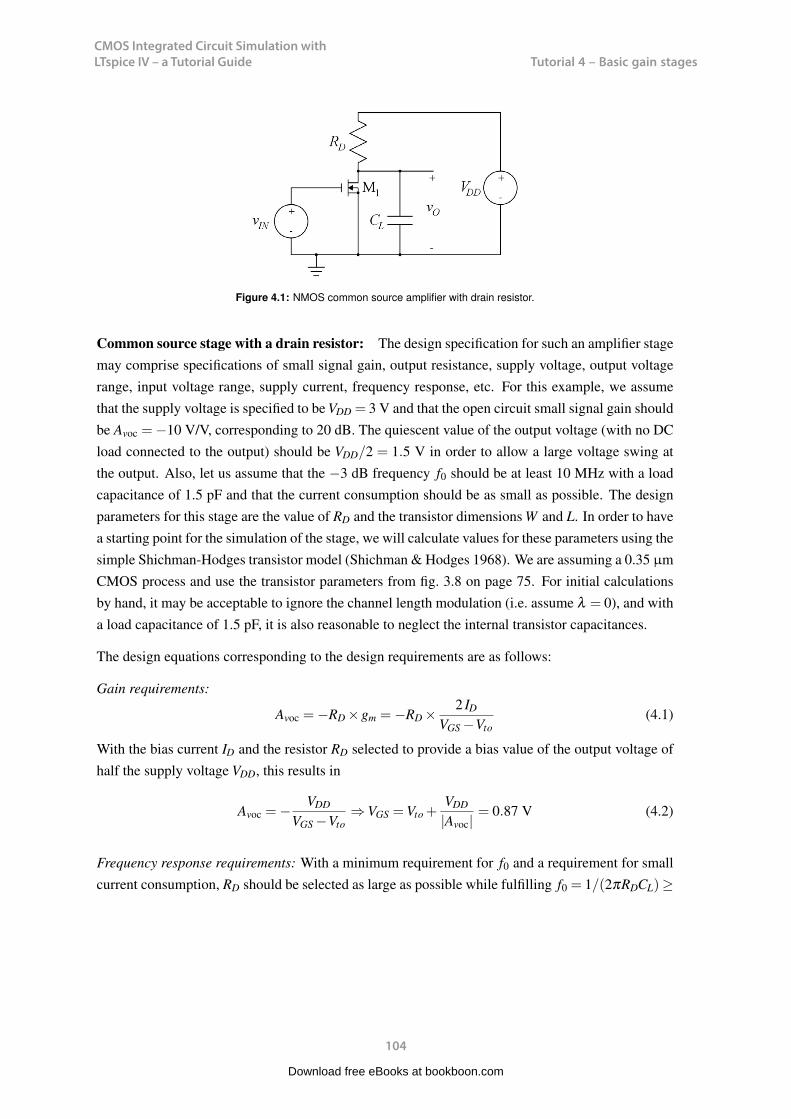
CMOS Integrated Circuit Simulation with LTspice IV – a Tutorial Guide
104
Tutorial 4 – Basic gain stagesCMOS Integrated Circuit Simulation with LTspice IV Tutorial 4
Figure 4.1: NMOS common source amplifier with drain resistor.
Common source stage with a drain resistor: The design specification for such an amplifier stagemay comprise specifications of small signal gain, output resistance, supply voltage, output voltagerange, input voltage range, supply current, frequency response, etc. For this example, we assumethat the supply voltage is specified to be VDD = 3 V and that the open circuit small signal gain shouldbe Avoc =−10 V/V, corresponding to 20 dB. The quiescent value of the output voltage (with no DCload connected to the output) should be VDD/2 = 1.5 V in order to allow a large voltage swing atthe output. Also, let us assume that the −3 dB frequency f0 should be at least 10 MHz with a loadcapacitance of 1.5 pF and that the current consumption should be as small as possible. The designparameters for this stage are the value of RD and the transistor dimensions W and L. In order to havea starting point for the simulation of the stage, we will calculate values for these parameters using thesimple Shichman-Hodges transistor model (Shichman & Hodges 1968). We are assuming a 0.35 µmCMOS process and use the transistor parameters from fig. 3.8 on page 75. For initial calculationsby hand, it may be acceptable to ignore the channel length modulation (i.e. assume λ = 0), and witha load capacitance of 1.5 pF, it is also reasonable to neglect the internal transistor capacitances.
The design equations corresponding to the design requirements are as follows:
Gain requirements:
Avoc =−RD ×gm =−RD × 2 ID
VGS −Vto(4.1)
With the bias current ID and the resistor RD selected to provide a bias value of the output voltage ofhalf the supply voltage VDD, this results in
Avoc =− VDD
VGS −Vto⇒VGS =Vto +
VDD
|Avoc|= 0.87 V (4.2)
Frequency response requirements: With a minimum requirement for f0 and a requirement for smallcurrent consumption, RD should be selected as large as possible while fulfilling f0 = 1/(2πRDCL)≥
104
Download free eBooks at bookboon.com

CMOS Integrated Circuit Simulation with LTspice IV – a Tutorial Guide
105
Tutorial 4 – Basic gain stagesCMOS Integrated Circuit Simulation with LTspice IV Tutorial 4
Figure 4.2: LTspice schematic for simulating the common source stage with the Shichman-Hodges transistor model.
10 MHz. From this,RD = 1/(2π f0CL) = 10.6 kΩ (4.3)
With this value of RD, the bias current ID is ID =VDD/(2RD) = 142 µA and the transistor transcon-ductance is gm = 0.94 mA/V. The transistor dimensions can be calculated from
WL
=2 ID
µnCox(VGS −Vto)2 = 16.6 (4.4)
105
Download free eBooks at bookboon.com
Click on the ad to read moreClick on the ad to read moreClick on the ad to read moreClick on the ad to read moreClick on the ad to read moreClick on the ad to read moreClick on the ad to read moreClick on the ad to read moreClick on the ad to read moreClick on the ad to read moreClick on the ad to read moreClick on the ad to read moreClick on the ad to read moreClick on the ad to read moreClick on the ad to read moreClick on the ad to read moreClick on the ad to read moreClick on the ad to read moreClick on the ad to read moreClick on the ad to read moreClick on the ad to read moreClick on the ad to read moreClick on the ad to read moreClick on the ad to read moreClick on the ad to read moreClick on the ad to read moreClick on the ad to read moreClick on the ad to read moreClick on the ad to read moreClick on the ad to read moreClick on the ad to read moreClick on the ad to read moreClick on the ad to read moreClick on the ad to read moreClick on the ad to read moreClick on the ad to read more
Get Help Now
Go to www.helpmyassignment.co.uk for more info
Need help with yourdissertation?Get in-depth feedback & advice from experts in your topic area. Find out what you can do to improvethe quality of your dissertation!
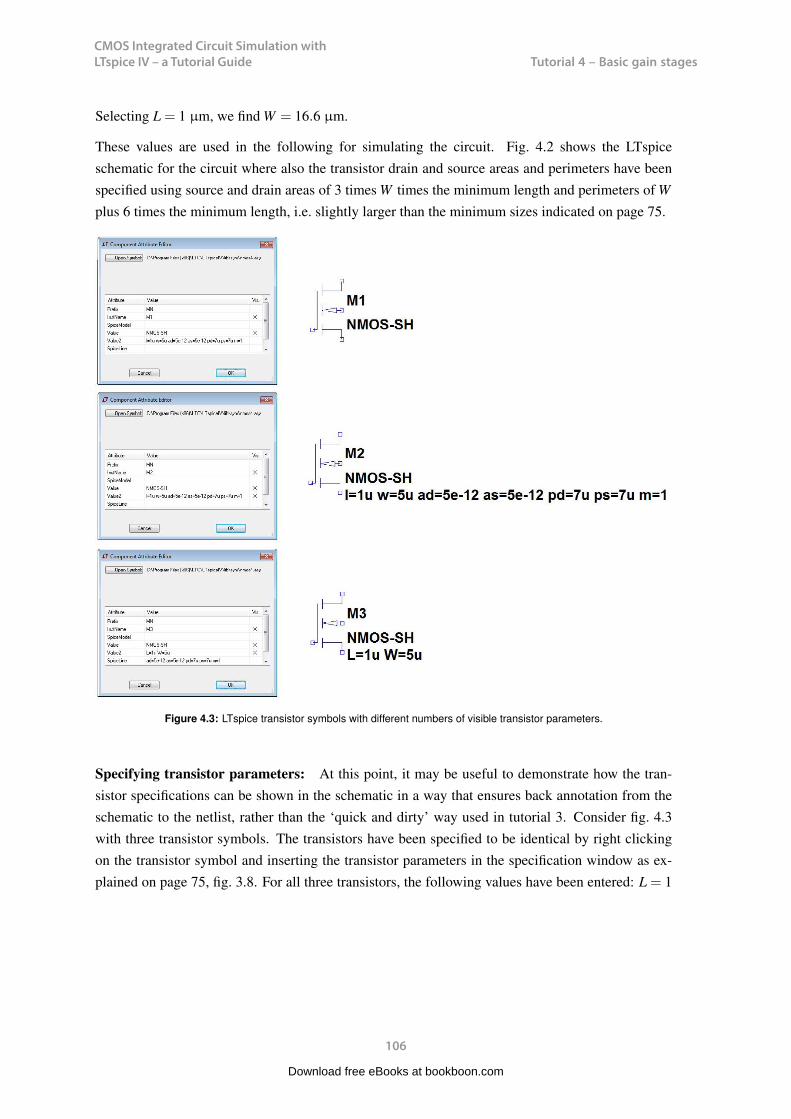
CMOS Integrated Circuit Simulation with LTspice IV – a Tutorial Guide
106
Tutorial 4 – Basic gain stagesCMOS Integrated Circuit Simulation with LTspice IV Tutorial 4
Selecting L = 1 µm, we find W = 16.6 µm.
These values are used in the following for simulating the circuit. Fig. 4.2 shows the LTspiceschematic for the circuit where also the transistor drain and source areas and perimeters have beenspecified using source and drain areas of 3 times W times the minimum length and perimeters of Wplus 6 times the minimum length, i.e. slightly larger than the minimum sizes indicated on page 75.
Figure 4.3: LTspice transistor symbols with different numbers of visible transistor parameters.
Specifying transistor parameters: At this point, it may be useful to demonstrate how the tran-sistor specifications can be shown in the schematic in a way that ensures back annotation from theschematic to the netlist, rather than the ‘quick and dirty’ way used in tutorial 3. Consider fig. 4.3with three transistor symbols. The transistors have been specified to be identical by right clickingon the transistor symbol and inserting the transistor parameters in the specification window as ex-plained on page 75, fig. 3.8. For all three transistors, the following values have been entered: L = 1
106
Download free eBooks at bookboon.com

CMOS Integrated Circuit Simulation with LTspice IV – a Tutorial Guide
107
Tutorial 4 – Basic gain stagesCMOS Integrated Circuit Simulation with LTspice IV Tutorial 4
µm, W = 5 µm, AD = AS = 5×10⁻¹² m2, PD = PS = 7 µm, M = 1. The topmost transistor (M1)shows only the name (M1) and the transistor model (NMOS-SH), and this is the LTspice default wayof showing the transistor. When you ‘Ctrl-right click’ on the transistor symbol, the ‘Component At-tribute Editor’ shown to the left of the symbol opens. In this, you will see the model name (NMOS-SH)listed as ‘Value’ and the transistor specification parameters listed as ‘Value2’. Notice the columnheading ‘Vis.’ (Visible). It has an X in the line for ‘InstName’ and ‘Value’ but not for ‘Value2’. Thisspecifies that only the name (M1) and the transistor model (NMOS-SH) are visible in the schematic.The middle transistor (M2) shows all the transistor parameters on the schematic. This is achieved byinserting an X in the ‘Component Attribute Editor’ for the line with ‘Value2’ as shown to the left ofthe transistor.The bottom transistor (M3) shows only L and W in addition to the name (M3) and the transistormodel (NMOS-SH). To the left of the transistor symbol is shown the ‘Component Attribute Editor’ forachieving this. The parameters which should be visible are remaining in the line ’Value2’ which isstill marked as visible, whereas the other parameters have been moved to the next line, ‘SpiceLine’,which is not marked as visible. Also, the letters for channel length and width have been changed tocapital letters. You may notice that the transistor specification in the netlist is the same for the threetransistors (’View → SPICE Netlist’).
Often in a CMOS circuit, you would use the same channel length for all transistor, so it may notbe necessary to show L in the schematic. If this is the case, L can just be moved to ‘SpiceLine’.The order of the parameters has no influence on the simulation. Having only W visible saves somedrawing space.
Clearly, this editing of the transistor is more involved than just the simple default specification.However, you can specify just one NMOS transistor and one PMOS transistor to show the parametersof interest, and then you can draw additional transistors using the duplicate command, ‘Edit →Duplicate’, ‘F6’, or toolbar symbol . An additional advantage is that the visible parameters arethen edited just by moving the cursor over the text and right clicking. If you use the specificationwindow shown in fig. 3.8 (page 75), all the parameters which are entered in the specification windoware placed in the line ‘Value2’ and will be visible in the schematic.
Iterativ design of the transistor channel width: In order to verify the calculations from (4.1) to(4.4), the circuit of fig. 4.2 may first be simulated using λ = 0. Running a DC sweep, you will findthat an input voltage of 0.87 V indeed results in an output voltage of 1.5 V, and from an AC analysis,you will find that the gain is indeed 20 dB with a −3 dB frequency of 10 MHz.
Changing λ to 0.16 V−1, a re-simulation of the DC sweep shows that the input bias voltage must be
107
Download free eBooks at bookboon.com

CMOS Integrated Circuit Simulation with LTspice IV – a Tutorial Guide
108
Tutorial 4 – Basic gain stages
CMOS Integrated Circuit Simulation with LTspice IV Tutorial 4
changed to 0.84 V in order to have an output voltage of 1.5 V. With this value of input bias voltage,a ‘.tf’ simulation shows a low frequency gain of −9.35 V/V and an output impedance of 8.87 kΩ.Obviously, the small signal output resistance rds of the transistor has some influence. Running a ‘.op’simulation and analyzing the transistor small signal parameters (‘Ctrl-L’ for viewing the error log),you find gds to be 18.4 µA/V, corresponding to rds = 54 kΩ. This is not quite negligible comparedto RD, and it will result in a smaller output resistance and a smaller gain. In order to obtain a largergain, the value of RD may be increased or the transistor width may be increased. Increasing RD
increases the output resistance and lowers the −3 dB frequency. Since λ is generally not a very wellcontrolled parameter, it is not advisable to increase RD as this may cause the output resistance to betoo high to fulfil the bandwidth requirement. Rather, the design may be modified by increasing thetransistor width which (for the same bias current ID) gives a larger value of gm and a larger value ofAvoc. From (3.8), we have
gm =
√2µnCox
WL
ID(1+λVDS) (4.5)
showing that gm is proportional to the square root of W/L. Thus, since gm needs to be increased byabout 7%, the value of W/L should be increased by about 14%, i.e. to about 19 µm. Again, a DCsweep is needed in order to find a new value for the input bias voltage. It is now VGS = 0.82 V foran output voltage of 1.5 V. With this value of VGS, an AC analysis results in a gain very close to 20dB and a −3 dB frequency of 11.6 MHz which fulfils the specifications.
108
CMOS Integrated Circuit Simulation with LTspice IV Tutorial 4
µm, W = 5 µm, AD = AS = 5×10⁻¹² m2, PD = PS = 7 µm, M = 1. The topmost transistor (M1)shows only the name (M1) and the transistor model (NMOS-SH), and this is the LTspice default wayof showing the transistor. When you ‘Ctrl-right click’ on the transistor symbol, the ‘Component At-tribute Editor’ shown to the left of the symbol opens. In this, you will see the model name (NMOS-SH)listed as ‘Value’ and the transistor specification parameters listed as ‘Value2’. Notice the columnheading ‘Vis.’ (Visible). It has an X in the line for ‘InstName’ and ‘Value’ but not for ‘Value2’. Thisspecifies that only the name (M1) and the transistor model (NMOS-SH) are visible in the schematic.The middle transistor (M2) shows all the transistor parameters on the schematic. This is achieved byinserting an X in the ‘Component Attribute Editor’ for the line with ‘Value2’ as shown to the left ofthe transistor.The bottom transistor (M3) shows only L and W in addition to the name (M3) and the transistormodel (NMOS-SH). To the left of the transistor symbol is shown the ‘Component Attribute Editor’ forachieving this. The parameters which should be visible are remaining in the line ’Value2’ which isstill marked as visible, whereas the other parameters have been moved to the next line, ‘SpiceLine’,which is not marked as visible. Also, the letters for channel length and width have been changed tocapital letters. You may notice that the transistor specification in the netlist is the same for the threetransistors (’View → SPICE Netlist’).
Often in a CMOS circuit, you would use the same channel length for all transistor, so it may notbe necessary to show L in the schematic. If this is the case, L can just be moved to ‘SpiceLine’.The order of the parameters has no influence on the simulation. Having only W visible saves somedrawing space.
Clearly, this editing of the transistor is more involved than just the simple default specification.However, you can specify just one NMOS transistor and one PMOS transistor to show the parametersof interest, and then you can draw additional transistors using the duplicate command, ‘Edit →Duplicate’, ‘F6’, or toolbar symbol . An additional advantage is that the visible parameters arethen edited just by moving the cursor over the text and right clicking. If you use the specificationwindow shown in fig. 3.8 (page 75), all the parameters which are entered in the specification windoware placed in the line ‘Value2’ and will be visible in the schematic.
Iterativ design of the transistor channel width: In order to verify the calculations from (4.1) to(4.4), the circuit of fig. 4.2 may first be simulated using λ = 0. Running a DC sweep, you will findthat an input voltage of 0.87 V indeed results in an output voltage of 1.5 V, and from an AC analysis,you will find that the gain is indeed 20 dB with a −3 dB frequency of 10 MHz.
Changing λ to 0.16 V−1, a re-simulation of the DC sweep shows that the input bias voltage must be
107
Download free eBooks at bookboon.com
Click on the ad to read moreClick on the ad to read moreClick on the ad to read moreClick on the ad to read moreClick on the ad to read moreClick on the ad to read moreClick on the ad to read moreClick on the ad to read moreClick on the ad to read moreClick on the ad to read moreClick on the ad to read moreClick on the ad to read moreClick on the ad to read moreClick on the ad to read moreClick on the ad to read moreClick on the ad to read moreClick on the ad to read moreClick on the ad to read moreClick on the ad to read moreClick on the ad to read moreClick on the ad to read moreClick on the ad to read moreClick on the ad to read moreClick on the ad to read moreClick on the ad to read moreClick on the ad to read moreClick on the ad to read moreClick on the ad to read moreClick on the ad to read moreClick on the ad to read moreClick on the ad to read moreClick on the ad to read moreClick on the ad to read moreClick on the ad to read moreClick on the ad to read moreClick on the ad to read moreClick on the ad to read more
By 2020, wind could provide one-tenth of our planet’s electricity needs. Already today, SKF’s innovative know-how is crucial to running a large proportion of the world’s wind turbines.
Up to 25 % of the generating costs relate to mainte-nance. These can be reduced dramatically thanks to our systems for on-line condition monitoring and automatic lubrication. We help make it more economical to create cleaner, cheaper energy out of thin air.
By sharing our experience, expertise, and creativity, industries can boost performance beyond expectations.
Therefore we need the best employees who can meet this challenge!
The Power of Knowledge Engineering
Brain power
Plug into The Power of Knowledge Engineering.
Visit us at www.skf.com/knowledge
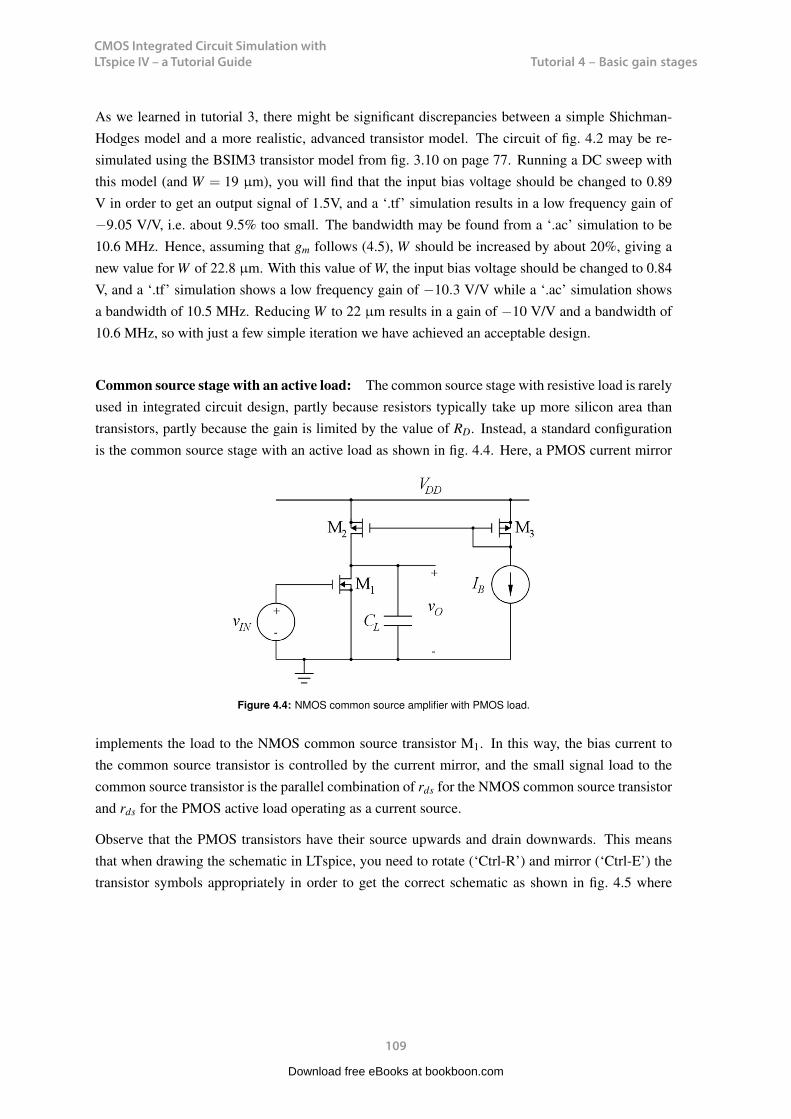
CMOS Integrated Circuit Simulation with LTspice IV – a Tutorial Guide
109
Tutorial 4 – Basic gain stagesCMOS Integrated Circuit Simulation with LTspice IV Tutorial 4
As we learned in tutorial 3, there might be significant discrepancies between a simple Shichman-Hodges model and a more realistic, advanced transistor model. The circuit of fig. 4.2 may be re-simulated using the BSIM3 transistor model from fig. 3.10 on page 77. Running a DC sweep withthis model (and W = 19 µm), you will find that the input bias voltage should be changed to 0.89V in order to get an output signal of 1.5V, and a ‘.tf’ simulation results in a low frequency gain of−9.05 V/V, i.e. about 9.5% too small. The bandwidth may be found from a ‘.ac’ simulation to be10.6 MHz. Hence, assuming that gm follows (4.5), W should be increased by about 20%, giving anew value for W of 22.8 µm. With this value of W, the input bias voltage should be changed to 0.84V, and a ‘.tf’ simulation shows a low frequency gain of −10.3 V/V while a ‘.ac’ simulation showsa bandwidth of 10.5 MHz. Reducing W to 22 µm results in a gain of −10 V/V and a bandwidth of10.6 MHz, so with just a few simple iteration we have achieved an acceptable design.
Common source stage with an active load: The common source stage with resistive load is rarelyused in integrated circuit design, partly because resistors typically take up more silicon area thantransistors, partly because the gain is limited by the value of RD. Instead, a standard configurationis the common source stage with an active load as shown in fig. 4.4. Here, a PMOS current mirror
Figure 4.4: NMOS common source amplifier with PMOS load.
implements the load to the NMOS common source transistor M1. In this way, the bias current tothe common source transistor is controlled by the current mirror, and the small signal load to thecommon source transistor is the parallel combination of rds for the NMOS common source transistorand rds for the PMOS active load operating as a current source.
Observe that the PMOS transistors have their source upwards and drain downwards. This meansthat when drawing the schematic in LTspice, you need to rotate (‘Ctrl-R’) and mirror (‘Ctrl-E’) thetransistor symbols appropriately in order to get the correct schematic as shown in fig. 4.5 where
109
Download free eBooks at bookboon.com

CMOS Integrated Circuit Simulation with LTspice IV – a Tutorial Guide
110
Tutorial 4 – Basic gain stagesCMOS Integrated Circuit Simulation with LTspice IV Tutorial 4
the connection to the PMOS gates is at the upper end of the gate electrode. You may have realizedthat the MOS transistor (with equal dimensions of drain and source diffusions) is a symmetricaldevice, so even if you do not perform the rotation and mirroring as in fig. 4.5, you would expect thesame performance of the circuit. Fig. 4.6 shows the schematic drawn without rotation of the PMOStransistors. The simulation results for the output voltage is the same for the two schematics, but withthe inverted drain and source terminals in fig. 4.6, the output files from a ‘.op’ simulation will besomewhat confusing. Fig. 4.7 shows the error log files with the transistor bias voltages and currentsand small signal parameters corresponding to both fig. 4.5 and fig. 4.6. The small signal parametersare identical, but the gate-source voltages and drain source voltages are different since drain andsource are interchanged. In general, the drawing standard of fig. 4.5 is recommended, even thoughit requires more manipulations in terms of rotation and mirroring since it gives output results whichare directly comparable to the results obtained from standard hand calculations.
You should also notice that just drawing a wire directly from the bulk terminal of a transistor to thesource terminal (the way it is done in fig. 4.1 and fig. 4.4) does not establish a connection betweenbulk and source. This is why the bulk connections in figs. 4.5 and 4.6 are drawn explicitly to groundand VDD. Fig. 4.8 shows a few ways to draw connections between bulk and source. Pay attention tothe incorrect drawings of M4, M5, M9 and M10. Also see the resulting netlist specification shownto the right in the figure. You can always check the connections by examining the netlist (’View →
110
Download free eBooks at bookboon.com
Click on the ad to read moreClick on the ad to read moreClick on the ad to read moreClick on the ad to read moreClick on the ad to read moreClick on the ad to read moreClick on the ad to read moreClick on the ad to read moreClick on the ad to read moreClick on the ad to read moreClick on the ad to read moreClick on the ad to read moreClick on the ad to read moreClick on the ad to read moreClick on the ad to read moreClick on the ad to read moreClick on the ad to read moreClick on the ad to read moreClick on the ad to read moreClick on the ad to read moreClick on the ad to read moreClick on the ad to read moreClick on the ad to read moreClick on the ad to read moreClick on the ad to read moreClick on the ad to read moreClick on the ad to read moreClick on the ad to read moreClick on the ad to read moreClick on the ad to read moreClick on the ad to read moreClick on the ad to read moreClick on the ad to read moreClick on the ad to read moreClick on the ad to read moreClick on the ad to read moreClick on the ad to read moreClick on the ad to read more
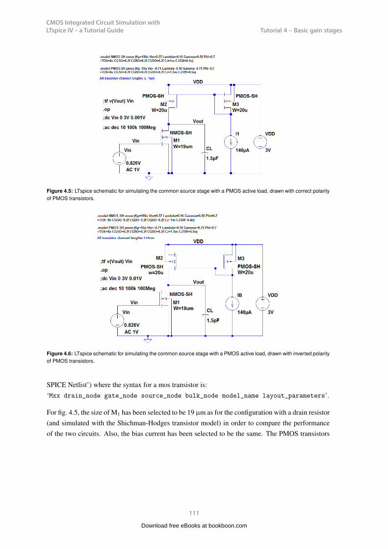
CMOS Integrated Circuit Simulation with LTspice IV – a Tutorial Guide
111
Tutorial 4 – Basic gain stagesCMOS Integrated Circuit Simulation with LTspice IV Tutorial 4
Figure 4.5: LTspice schematic for simulating the common source stage with a PMOS active load, drawn with correct polarityof PMOS transistors.
Figure 4.6: LTspice schematic for simulating the common source stage with a PMOS active load, drawn with inverted polarityof PMOS transistors.
SPICE Netlist’) where the syntax for a mos transistor is:‘Mxx drain_node gate_node source_node bulk_node model_name layout_parameters’.
For fig. 4.5, the size of M1 has been selected to be 19 µm as for the configuration with a drain resistor(and simulated with the Shichman-Hodges transistor model) in order to compare the performanceof the two circuits. Also, the bias current has been selected to be the same. The PMOS transistors
111
Download free eBooks at bookboon.com
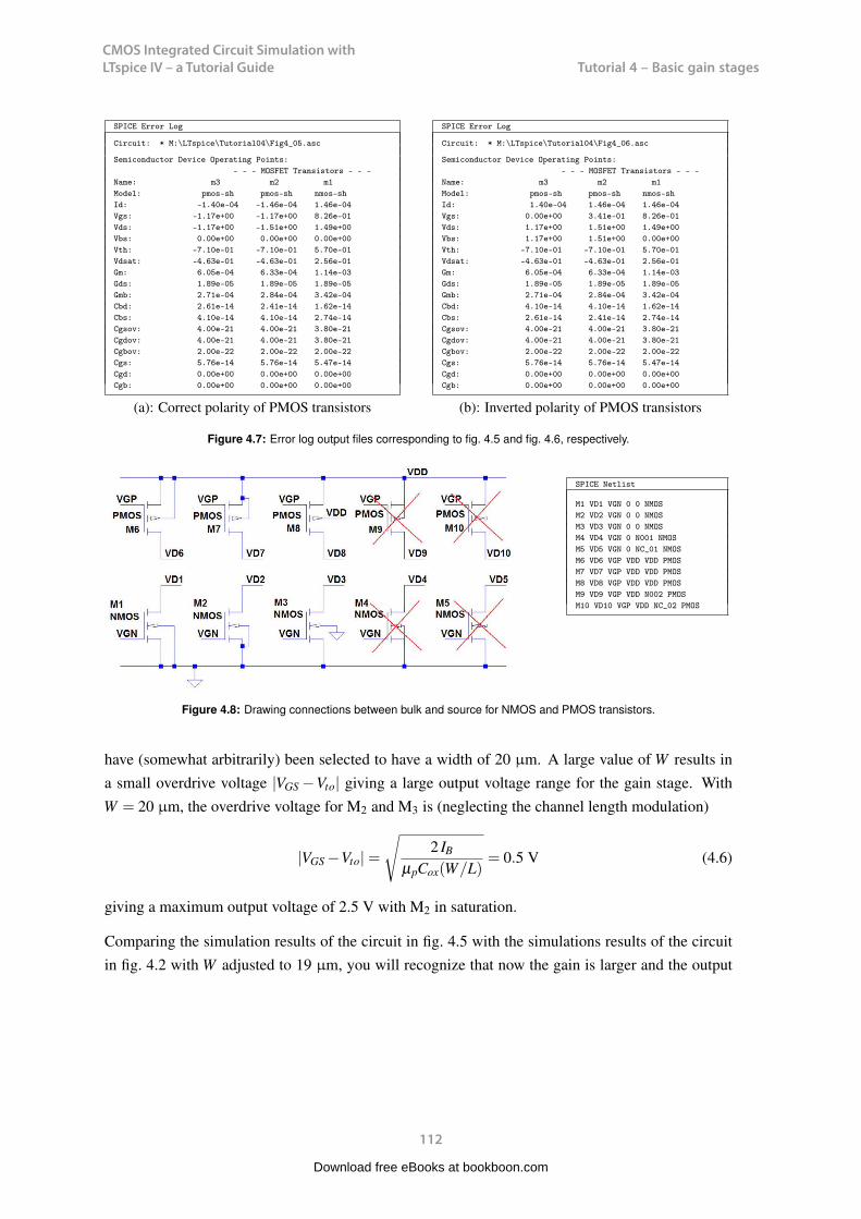
CMOS Integrated Circuit Simulation with LTspice IV – a Tutorial Guide
112
Tutorial 4 – Basic gain stagesCMOS Integrated Circuit Simulation with LTspice IV Tutorial 4
SPICE Error Log
Circuit: * M:\LTspice\Tutorial04\Fig4_05.asc
Semiconductor Device Operating Points:- - - MOSFET Transistors - - -
Name: m3 m2 m1Model: pmos-sh pmos-sh nmos-shId: -1.40e-04 -1.46e-04 1.46e-04Vgs: -1.17e+00 -1.17e+00 8.26e-01Vds: -1.17e+00 -1.51e+00 1.49e+00Vbs: 0.00e+00 0.00e+00 0.00e+00Vth: -7.10e-01 -7.10e-01 5.70e-01Vdsat: -4.63e-01 -4.63e-01 2.56e-01Gm: 6.05e-04 6.33e-04 1.14e-03Gds: 1.89e-05 1.89e-05 1.89e-05Gmb: 2.71e-04 2.84e-04 3.42e-04Cbd: 2.61e-14 2.41e-14 1.62e-14Cbs: 4.10e-14 4.10e-14 2.74e-14Cgsov: 4.00e-21 4.00e-21 3.80e-21Cgdov: 4.00e-21 4.00e-21 3.80e-21Cgbov: 2.00e-22 2.00e-22 2.00e-22Cgs: 5.76e-14 5.76e-14 5.47e-14Cgd: 0.00e+00 0.00e+00 0.00e+00Cgb: 0.00e+00 0.00e+00 0.00e+00
(a): Correct polarity of PMOS transistors
SPICE Error Log
Circuit: * M:\LTspice\Tutorial04\Fig4_06.asc
Semiconductor Device Operating Points:- - - MOSFET Transistors - - -
Name: m3 m2 m1Model: pmos-sh pmos-sh nmos-shId: 1.40e-04 1.46e-04 1.46e-04Vgs: 0.00e+00 3.41e-01 8.26e-01Vds: 1.17e+00 1.51e+00 1.49e+00Vbs: 1.17e+00 1.51e+00 0.00e+00Vth: -7.10e-01 -7.10e-01 5.70e-01Vdsat: -4.63e-01 -4.63e-01 2.56e-01Gm: 6.05e-04 6.33e-04 1.14e-03Gds: 1.89e-05 1.89e-05 1.89e-05Gmb: 2.71e-04 2.84e-04 3.42e-04Cbd: 4.10e-14 4.10e-14 1.62e-14Cbs: 2.61e-14 2.41e-14 2.74e-14Cgsov: 4.00e-21 4.00e-21 3.80e-21Cgdov: 4.00e-21 4.00e-21 3.80e-21Cgbov: 2.00e-22 2.00e-22 2.00e-22Cgs: 5.76e-14 5.76e-14 5.47e-14Cgd: 0.00e+00 0.00e+00 0.00e+00Cgb: 0.00e+00 0.00e+00 0.00e+00
(b): Inverted polarity of PMOS transistors
Figure 4.7: Error log output files corresponding to fig. 4.5 and fig. 4.6, respectively.
SPICE Netlist
M1 VD1 VGN 0 0 NMOSM2 VD2 VGN 0 0 NMOSM3 VD3 VGN 0 0 NMOSM4 VD4 VGN 0 N001 NMOSM5 VD5 VGN 0 NC_01 NMOSM6 VD6 VGP VDD VDD PMOSM7 VD7 VGP VDD VDD PMOSM8 VD8 VGP VDD VDD PMOSM9 VD9 VGP VDD N002 PMOSM10 VD10 VGP VDD NC_02 PMOS
Figure 4.8: Drawing connections between bulk and source for NMOS and PMOS transistors.
have (somewhat arbitrarily) been selected to have a width of 20 µm. A large value of W results ina small overdrive voltage |VGS −Vto| giving a large output voltage range for the gain stage. WithW = 20 µm, the overdrive voltage for M2 and M3 is (neglecting the channel length modulation)
|VGS −Vto|=
√2 IB
µpCox(W/L)= 0.5 V (4.6)
giving a maximum output voltage of 2.5 V with M2 in saturation.
Comparing the simulation results of the circuit in fig. 4.5 with the simulations results of the circuitin fig. 4.2 with W adjusted to 19 µm, you will recognize that now the gain is larger and the output
112
Download free eBooks at bookboon.com

CMOS Integrated Circuit Simulation with LTspice IV – a Tutorial Guide
113
Tutorial 4 – Basic gain stagesCMOS Integrated Circuit Simulation with LTspice IV Tutorial 4
resistance is higher. The ‘.tf’ simulation results in Avoc =−30.3 V/V and ro = 26,5 kΩ. The reasonfor this is that in the expression for the gain, RD is now replaced by the small signal output resistanceof M2, and the total small signal output resistance is the parallel combination of the output resistanceof M1 and M2. They are both caused by the transistor channel length modulation which is not a wellcontrolled transistor parameter. This implies that for the common source configuration with an activeload, a design target for the 3 dB bandwidth cannot be met with a reasonable precision. The ‘.ac’simulation of fig. 4.5 shows a 3 dB bandwidth of 3.9 MHz rather than 11.6 MHz as found on page108. Instead, it is the product of gain and bandwidth which is a relevant design target. It is givenby 2π ×GBW = gm1/CL, and both gm1 and CL are reasonably well controlled. For the commonsource stage with a drain resistor as in fig. 4.2, the gain bandwidth product is 10×11.6 MHz = 116MHz. For the common source stage with an active load as in fig. 4.5, the gain bandwidth product is30.3×3.9 MHz=118 MHz, i.e. very close to the value obtained for the circuit with a drain resistor.
Next, the circuit may be simulated using the BSIM3 transistor models. With the same transistorgeometries, the simulations result in a gain of −60.3 V/V and a bandwidth of 1.57 MHz, givinga gain bandwidth product of 95 MHz which is somewhat smaller than with the Shichman-Hodgesmodel. As for the configuration with a drain resistor, the design may be modified by increasing W1,and using the same value for W1 as for the configuration with a drain resistor (i.e. W1 = 22 µm),we find a gain of −65.2 V/V and a bandwidth of 1.60 MHz, resulting in a gain bandwidth product
113
Download free eBooks at bookboon.com
Click on the ad to read moreClick on the ad to read moreClick on the ad to read moreClick on the ad to read moreClick on the ad to read moreClick on the ad to read moreClick on the ad to read moreClick on the ad to read moreClick on the ad to read moreClick on the ad to read moreClick on the ad to read moreClick on the ad to read moreClick on the ad to read moreClick on the ad to read moreClick on the ad to read moreClick on the ad to read moreClick on the ad to read moreClick on the ad to read moreClick on the ad to read moreClick on the ad to read moreClick on the ad to read moreClick on the ad to read moreClick on the ad to read moreClick on the ad to read moreClick on the ad to read moreClick on the ad to read moreClick on the ad to read moreClick on the ad to read moreClick on the ad to read moreClick on the ad to read moreClick on the ad to read moreClick on the ad to read moreClick on the ad to read moreClick on the ad to read moreClick on the ad to read moreClick on the ad to read moreClick on the ad to read moreClick on the ad to read moreClick on the ad to read more
EXPERIENCE THE POWER OF FULL ENGAGEMENT…
RUN FASTER. RUN LONGER.. RUN EASIER…
READ MORE & PRE-ORDER TODAY WWW.GAITEYE.COM
Challenge the way we run
1349906_A6_4+0.indd 1 22-08-2014 12:56:57
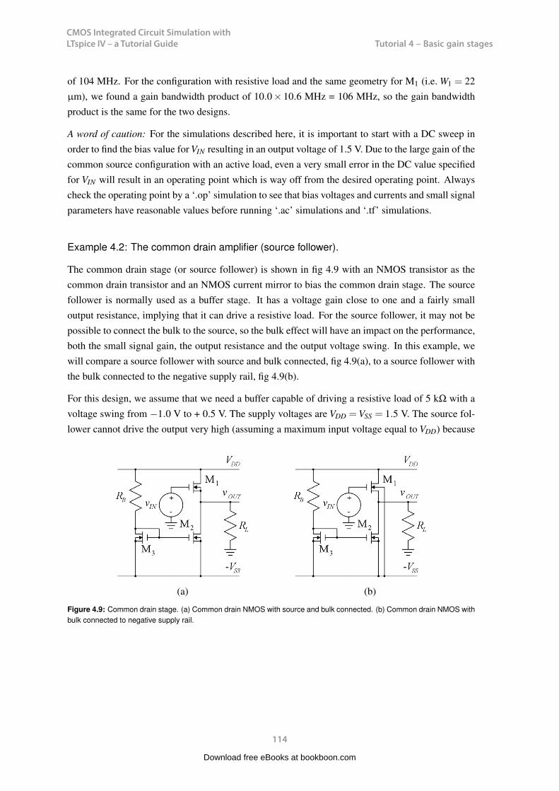
CMOS Integrated Circuit Simulation with LTspice IV – a Tutorial Guide
114
Tutorial 4 – Basic gain stagesCMOS Integrated Circuit Simulation with LTspice IV Tutorial 4
of 104 MHz. For the configuration with resistive load and the same geometry for M1 (i.e. W1 = 22µm), we found a gain bandwidth product of 10.0× 10.6 MHz = 106 MHz, so the gain bandwidthproduct is the same for the two designs.
A word of caution: For the simulations described here, it is important to start with a DC sweep inorder to find the bias value for VIN resulting in an output voltage of 1.5 V. Due to the large gain of thecommon source configuration with an active load, even a very small error in the DC value specifiedfor VIN will result in an operating point which is way off from the desired operating point. Alwayscheck the operating point by a ‘.op’ simulation to see that bias voltages and currents and small signalparameters have reasonable values before running ‘.ac’ simulations and ‘.tf’ simulations.
Example 4.2: The common drain amplifier (source follower).
The common drain stage (or source follower) is shown in fig 4.9 with an NMOS transistor as thecommon drain transistor and an NMOS current mirror to bias the common drain stage. The sourcefollower is normally used as a buffer stage. It has a voltage gain close to one and a fairly smalloutput resistance, implying that it can drive a resistive load. For the source follower, it may not bepossible to connect the bulk to the source, so the bulk effect will have an impact on the performance,both the small signal gain, the output resistance and the output voltage swing. In this example, wewill compare a source follower with source and bulk connected, fig 4.9(a), to a source follower withthe bulk connected to the negative supply rail, fig 4.9(b).
For this design, we assume that we need a buffer capable of driving a resistive load of 5 kΩ with avoltage swing from −1.0 V to + 0.5 V. The supply voltages are VDD =VSS = 1.5 V. The source fol-lower cannot drive the output very high (assuming a maximum input voltage equal to VDD) because
(a) (b)
Figure 4.9: Common drain stage. (a) Common drain NMOS with source and bulk connected. (b) Common drain NMOS withbulk connected to negative supply rail.
114
Download free eBooks at bookboon.com

CMOS Integrated Circuit Simulation with LTspice IV – a Tutorial Guide
115
Tutorial 4 – Basic gain stagesCMOS Integrated Circuit Simulation with LTspice IV Tutorial 4
a gate-source voltage is needed between the input voltage and the output voltage. First, we designthe buffer shown in fig. 4.9(a) assuming a Shichman-Hodges transistor model with the parametersfrom fig. 3.8 on page 75. Next, we take the bulk effect into consideration (fig. 4.9(b)), and finallywe use the BSIM3 transistor model from fig. 3.10 on page 77 for an extra design iteration.
The basic design requirements arise from the output swing. In order to have a negative output swingof −1.0 V with a load resistor of 5 kΩ, we need a bias current in M2 of at least 1 V/5 kΩ = 0.2 mA. AsM2 is configured as a current source, it should be in the active area for this bias current, implying thatthe overdrive voltage VGS2−Vto must be at most 0.5 V in order ensure VDS2 ≥VGS2−Vto. Neglectingthe channel length modulation, we may calculate a minimum value of (W2/L2) from
W2
L2=
2 ID2
µnCox(VGS2 −Vto)2 = 8.4 (4.7)
For an initial design, we select L2 = 1 µm and W2 = 10 µm. For M3, we may use a smaller width,scaling down the current in M3 and RB compared to the current in M3 in order to reduce the currentconsumption of the bias circuit. Using a scale factor of 10, we select L3 =W3 = 1 µm. The resistorRB is calculated from VGS3, the supply voltage and the current:
RB =VDD +VSS −VGS3
ID3=
VDD +VSS −Vto −√
2 ID3µnCox(W3/L3)
ID3= 98.5 kΩ (4.8)
Finally, M1 must be designed so that it can supply 200 µA to M2 plus 100 µA to RL (giving anoutput voltage of 0.5 V) when the gate voltage is the maximum input voltage which is assumed tobe VDD. This implies (compare (4.7))
W1
L1=
2×300 µA190 µA/V2(1.5 V−0.5 V−0.57 V)2
= 17 (4.9)
With L1 = 1 µA, we select W1 = 17 µm.
Fig. 4.10 shows the schematic corresponding to fig 4.9(a) and with the Shichman-Hodges transistormodel for the specification of M1, M2 and M3. For an initial simulation, it may be a good idea touse λ = 0 in the model description as shown in the figure. In this way, the hand calculations canbe verified directly. For verifying the lower output voltage limit, a ‘.op’ simulation with the inputat −1.5 V may be run, and for verifying the upper output limit, a ‘.op’ simulation with the input at+1.5 V may be run. Fig. 4.11 shows the output files and the error log files from these simulations.Notice that labels have been placed on all the nodes in the schematic in fig. 4.10, using the command‘Edit → Label Net’ (or toolbar symbol ). This makes it easier to read the output file from thesimulation.
115
Download free eBooks at bookboon.com
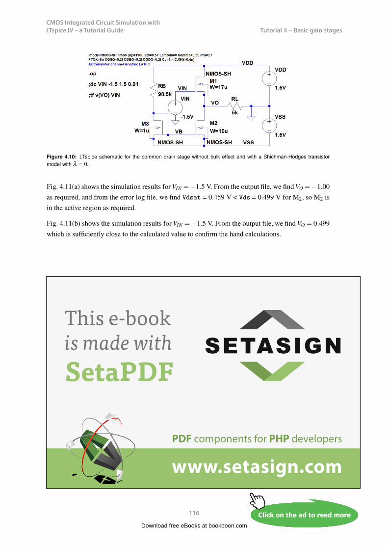
CMOS Integrated Circuit Simulation with LTspice IV – a Tutorial Guide
116
Tutorial 4 – Basic gain stagesCMOS Integrated Circuit Simulation with LTspice IV Tutorial 4
Figure 4.10: LTspice schematic for the common drain stage without bulk effect and with a Shichman-Hodges transistormodel with λ = 0.
Fig. 4.11(a) shows the simulation results for VIN =−1.5 V. From the output file, we find VO =−1.00as required, and from the error log file, we find Vdsat = 0.459 V < Vds = 0.499 V for M2, so M2 isin the active region as required.
Fig. 4.11(b) shows the simulation results for VIN =+1.5 V. From the output file, we find VO = 0.499which is sufficiently close to the calculated value to confirm the hand calculations.
For the schematic, you may also run a DC sweep with the input voltage swept from −1.5 V to
116
Download free eBooks at bookboon.com
Click on the ad to read moreClick on the ad to read moreClick on the ad to read moreClick on the ad to read moreClick on the ad to read moreClick on the ad to read moreClick on the ad to read moreClick on the ad to read moreClick on the ad to read moreClick on the ad to read moreClick on the ad to read moreClick on the ad to read moreClick on the ad to read moreClick on the ad to read moreClick on the ad to read moreClick on the ad to read moreClick on the ad to read moreClick on the ad to read moreClick on the ad to read moreClick on the ad to read moreClick on the ad to read moreClick on the ad to read moreClick on the ad to read moreClick on the ad to read moreClick on the ad to read moreClick on the ad to read moreClick on the ad to read moreClick on the ad to read moreClick on the ad to read moreClick on the ad to read moreClick on the ad to read moreClick on the ad to read moreClick on the ad to read moreClick on the ad to read moreClick on the ad to read moreClick on the ad to read moreClick on the ad to read moreClick on the ad to read moreClick on the ad to read moreClick on the ad to read more
PDF components for PHP developers
www.setasign.com
SETASIGNThis e-book is made with SetaPDF
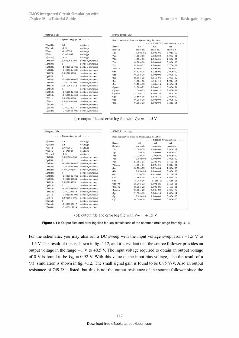
CMOS Integrated Circuit Simulation with LTspice IV – a Tutorial Guide
117
Tutorial 4 – Basic gain stagesCMOS Integrated Circuit Simulation with LTspice IV Tutorial 4
Output file:
- - - Operating point - - -
V(vdd): 1.5 voltageV(vin): -1.5 voltageV(vo): -1.00053 voltageV(vb): -0.471047 voltageV(-vss): -1.5 voltageId(M3): 2.00106e-005 device_currentIg(M3): 0 device_currentIb(M3): -1.03895e-012 device_currentIs(M3): -2.00106e-005 device_currentId(M2): 0.000200106 device_currentIg(M2): 0 device_currentIb(M2): -5.09469e-013 device_currentIs(M2): -0.000200106 device_currentId(M1): 5.01106e-012 device_currentIg(M1): 0 device_currentIb(M1): -2.51053e-012 device_currentIs(M1): -2.50053e-012 device_currentI(Rl): 0.000200106 device_currentI(Rb): 2.00106e-005 device_currentI(Vin): 0 device_currentI(Vss): -0.000220117 device_currentI(Vdd): -2.00106e-005 device_current
SPICE Error Log
Semiconductor Device Operating Points:- - - MOSFET Transistors - - -
Name: m3 m2 m1Model: nmos-sh nmos-sh nmos-shId: 2.00e-05 2.00e-04 5.01e-12Vgs: 1.03e+00 1.03e+00 -4.99e-01Vds: 1.03e+00 4.99e-01 2.50e+00Vbs: 0.00e+00 0.00e+00 0.00e+00Vth: 5.70e-01 5.70e-01 5.70e-01Vdsat: 4.59e-01 4.59e-01 0.00e+00Gm: 8.72e-05 8.72e-04 0.00e+00Gds: 0.00e+00 0.00e+00 0.00e+00Gmb: 2.61e-05 2.61e-04 0.00e+00Cbd: 1.46e-15 1.16e-14 1.21e-14Cbs: 2.20e-15 1.48e-14 2.46e-14Cgsov: 2.00e-22 2.00e-21 3.40e-21Cgdov: 2.00e-22 2.00e-21 3.40e-21Cgbov: 2.00e-22 2.00e-22 2.00e-22Cgs: 2.88e-15 2.88e-14 0.00e+00Cgd: 0.00e+00 0.00e+00 0.00e+00Cgb: 0.00e+00 0.00e+00 7.34e-14
(a): output file and error log file with VIN =−1.5 V.
Output file:
- - - Operating point - - -
V(vdd): 1.5 voltageV(vin): 1.5 voltageV(vo): 0.499061 voltageV(vb): -0.471047 voltageV(-vss): -1.5 voltageId(M3): 2.00106e-005 device_currentIg(M3): 0 device_currentIb(M3): -1.03895e-012 device_currentIs(M3): -2.00106e-005 device_currentId(M2): 0.000200106 device_currentIg(M2): 0 device_currentIb(M2): -2.00906e-012 device_currentIs(M2): -0.000200106 device_currentId(M1): 0.000299919 device_currentIg(M1): 0 device_currentIb(M1): -1.01094e-012 device_currentIs(M1): -0.000299919 device_currentI(Rl): -9.98123e-005 device_currentI(Rb): 2.00106e-005 device_currentI(Vin): 0 device_currentI(Vss): -0.000220117 device_currentI(Vdd): -0.000319929 device_current
SPICE Error Log
Semiconductor Device Operating Points:- - - MOSFET Transistors - - -
Name: m3 m2 m1Model: nmos-sh nmos-sh nmos-shId: 2.00e-05 2.00e-04 3.00e-04Vgs: 1.03e+00 1.03e+00 1.00e+00Vds: 1.03e+00 2.00e+00 1.00e+00Vbs: 0.00e+00 0.00e+00 0.00e+00Vth: 5.70e-01 5.70e-01 5.70e-01Vdsat: 4.59e-01 4.59e-01 4.31e-01Gm: 8.72e-05 8.72e-04 1.39e-03Gds: 0.00e+00 0.00e+00 0.00e+00Gmb: 2.61e-05 2.61e-04 4.16e-04Cbd: 1.46e-15 7.91e-15 1.64e-14Cbs: 2.20e-15 1.48e-14 2.46e-14Cgsov: 2.00e-22 2.00e-21 3.40e-21Cgdov: 2.00e-22 2.00e-21 3.40e-21Cgbov: 2.00e-22 2.00e-22 2.00e-22Cgs: 2.88e-15 2.88e-14 4.89e-14Cgd: 0.00e+00 0.00e+00 0.00e+00Cgb: 0.00e+00 0.00e+00 0.00e+00
(b): output file and error log file with VIN =+1.5 V.
Figure 4.11: Output files and error log files for ‘.op’ simulations of the common drain stage from fig. 4.10
+1.5 V. The result of this is shown in fig. 4.12, and it is evident that the source follower provides anoutput voltage in the range −1 V to +0.5 V. The input voltage required to obtain an output voltageof 0 V is found to be VIN = 0.92 V. With this value of the input bias voltage, also the result of a‘.tf’ simulation is shown in fig. 4.12. The small signal gain is found to be 0.85 V/V. Also an outputresistance of 749 Ω is listed, but this is not the output resistance of the source follower since the
117
CMOS Integrated Circuit Simulation with LTspice IV Tutorial 4
Figure 4.10: LTspice schematic for the common drain stage without bulk effect and with a Shichman-Hodges transistormodel with λ = 0.
Fig. 4.11(a) shows the simulation results for VIN =−1.5 V. From the output file, we find VO =−1.00as required, and from the error log file, we find Vdsat = 0.459 V < Vds = 0.499 V for M2, so M2 isin the active region as required.
Fig. 4.11(b) shows the simulation results for VIN =+1.5 V. From the output file, we find VO = 0.499which is sufficiently close to the calculated value to confirm the hand calculations.
For the schematic, you may also run a DC sweep with the input voltage swept from −1.5 V to
116
CMOS Integrated Circuit Simulation with LTspice IV Tutorial 4
Output file:
- - - Operating point - - -
V(vdd): 1.5 voltageV(vin): -1.5 voltageV(vo): -1.00053 voltageV(vb): -0.471047 voltageV(-vss): -1.5 voltageId(M3): 2.00106e-005 device_currentIg(M3): 0 device_currentIb(M3): -1.03895e-012 device_currentIs(M3): -2.00106e-005 device_currentId(M2): 0.000200106 device_currentIg(M2): 0 device_currentIb(M2): -5.09469e-013 device_currentIs(M2): -0.000200106 device_currentId(M1): 5.01106e-012 device_currentIg(M1): 0 device_currentIb(M1): -2.51053e-012 device_currentIs(M1): -2.50053e-012 device_currentI(Rl): 0.000200106 device_currentI(Rb): 2.00106e-005 device_currentI(Vin): 0 device_currentI(Vss): -0.000220117 device_currentI(Vdd): -2.00106e-005 device_current
SPICE Error Log
Semiconductor Device Operating Points:- - - MOSFET Transistors - - -
Name: m3 m2 m1Model: nmos-sh nmos-sh nmos-shId: 2.00e-05 2.00e-04 5.01e-12Vgs: 1.03e+00 1.03e+00 -4.99e-01Vds: 1.03e+00 4.99e-01 2.50e+00Vbs: 0.00e+00 0.00e+00 0.00e+00Vth: 5.70e-01 5.70e-01 5.70e-01Vdsat: 4.59e-01 4.59e-01 0.00e+00Gm: 8.72e-05 8.72e-04 0.00e+00Gds: 0.00e+00 0.00e+00 0.00e+00Gmb: 2.61e-05 2.61e-04 0.00e+00Cbd: 1.46e-15 1.16e-14 1.21e-14Cbs: 2.20e-15 1.48e-14 2.46e-14Cgsov: 2.00e-22 2.00e-21 3.40e-21Cgdov: 2.00e-22 2.00e-21 3.40e-21Cgbov: 2.00e-22 2.00e-22 2.00e-22Cgs: 2.88e-15 2.88e-14 0.00e+00Cgd: 0.00e+00 0.00e+00 0.00e+00Cgb: 0.00e+00 0.00e+00 7.34e-14
(a): output file and error log file with VIN =−1.5 V.
Output file:
- - - Operating point - - -
V(vdd): 1.5 voltageV(vin): 1.5 voltageV(vo): 0.499061 voltageV(vb): -0.471047 voltageV(-vss): -1.5 voltageId(M3): 2.00106e-005 device_currentIg(M3): 0 device_currentIb(M3): -1.03895e-012 device_currentIs(M3): -2.00106e-005 device_currentId(M2): 0.000200106 device_currentIg(M2): 0 device_currentIb(M2): -2.00906e-012 device_currentIs(M2): -0.000200106 device_currentId(M1): 0.000299919 device_currentIg(M1): 0 device_currentIb(M1): -1.01094e-012 device_currentIs(M1): -0.000299919 device_currentI(Rl): -9.98123e-005 device_currentI(Rb): 2.00106e-005 device_currentI(Vin): 0 device_currentI(Vss): -0.000220117 device_currentI(Vdd): -0.000319929 device_current
SPICE Error Log
Semiconductor Device Operating Points:- - - MOSFET Transistors - - -
Name: m3 m2 m1Model: nmos-sh nmos-sh nmos-shId: 2.00e-05 2.00e-04 3.00e-04Vgs: 1.03e+00 1.03e+00 1.00e+00Vds: 1.03e+00 2.00e+00 1.00e+00Vbs: 0.00e+00 0.00e+00 0.00e+00Vth: 5.70e-01 5.70e-01 5.70e-01Vdsat: 4.59e-01 4.59e-01 4.31e-01Gm: 8.72e-05 8.72e-04 1.39e-03Gds: 0.00e+00 0.00e+00 0.00e+00Gmb: 2.61e-05 2.61e-04 4.16e-04Cbd: 1.46e-15 7.91e-15 1.64e-14Cbs: 2.20e-15 1.48e-14 2.46e-14Cgsov: 2.00e-22 2.00e-21 3.40e-21Cgdov: 2.00e-22 2.00e-21 3.40e-21Cgbov: 2.00e-22 2.00e-22 2.00e-22Cgs: 2.88e-15 2.88e-14 4.89e-14Cgd: 0.00e+00 0.00e+00 0.00e+00Cgb: 0.00e+00 0.00e+00 0.00e+00
(b): output file and error log file with VIN =+1.5 V.
Figure 4.11: Output files and error log files for ‘.op’ simulations of the common drain stage from fig. 4.10
+1.5 V. The result of this is shown in fig. 4.12, and it is evident that the source follower provides anoutput voltage in the range −1 V to +0.5 V. The input voltage required to obtain an output voltageof 0 V is found to be VIN = 0.92 V. With this value of the input bias voltage, also the result of a‘.tf’ simulation is shown in fig. 4.12. The small signal gain is found to be 0.85 V/V. Also an outputresistance of 749 Ω is listed, but this is not the output resistance of the source follower since the
117
Download free eBooks at bookboon.com
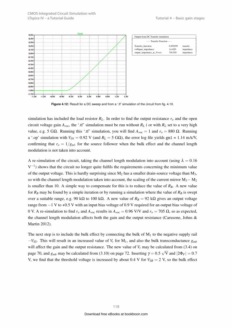
CMOS Integrated Circuit Simulation with LTspice IV – a Tutorial Guide
118
Tutorial 4 – Basic gain stagesCMOS Integrated Circuit Simulation with LTspice IV Tutorial 4
Output from DC Transfer simulation
- - - Transfer Function - - -
Transfer_function: 0.850299 transfervs#Input_impedance: 1e+020 impedanceoutput_impedance_at_V(vo): 748.505 impedance
Figure 4.12: Result for a DC sweep and from a ‘.tf’ simulation of the circuit from fig. 4.10.
simulation has included the load resistor RL. In order to find the output resistance ro and the opencircuit voltage gain Avoc, the ‘.tf’ simulation must be run without RL ( or with RL set to a very highvalue, e.g. 5 GΩ. Running this ‘.tf’ simulation, you will find Avoc = 1 and ro = 880 Ω. Runninga ‘.op’ simulation with VIN = 0.92 V (and RL = 5 GΩ), the error log file yields gm1 = 1.14 mA/V,confirming that ro = 1/gm1 for the source follower when the bulk effect and the channel lengthmodulation is not taken into account.
A re-simulation of the circuit, taking the channel length modulation into account (using λ = 0.16V−1) shows that the circuit no longer quite fulfils the requirements concerning the minimum valueof the output voltage. This is hardly surprising since M2 has a smaller drain-source voltage than M3,so with the channel length modulation taken into account, the scaling of the current mirror M3− M2
is smaller than 10. A simple way to compensate for this is to reduce the value of RB. A new valuefor RB may be found by a simple iteration or by running a simulation where the value of RB is sweptover a suitable range, e.g. 90 kΩ to 100 kΩ. A new value of RB = 92 kΩ gives an output voltagerange from −1 V to +0.5 V with an input bias voltage of 0.9 V required for an output bias voltage of0 V. A re-simulation to find ro and Avoc results in Avoc = 0.96 V/V and ro = 705 Ω, so as expected,the channel length modulation affects both the gain and the output resistance (Carusone, Johns &Martin 2012).
The next step is to include the bulk effect by connecting the bulk of M1 to the negative supply rail−VSS. This will result in an increased value of Vt for M1, and also the bulk transconductance gmb
will affect the gain and the output resistance. The new value of Vt may be calculated from (3.4) onpage 70, and gmb may be calculated from (3.10) on page 72. Inserting γ = 0.5
√V and |2ΦF |= 0.7
V, we find that the threshold voltage is increased by about 0.4 V for VSB = 2 V, so the bulk effect
118
Download free eBooks at bookboon.com
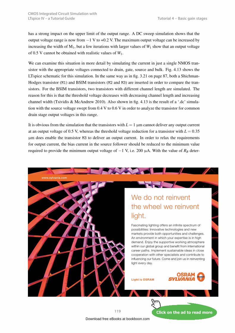
CMOS Integrated Circuit Simulation with LTspice IV – a Tutorial Guide
119
Tutorial 4 – Basic gain stagesCMOS Integrated Circuit Simulation with LTspice IV Tutorial 4
has a strong impact on the upper limit of the output range. A DC sweep simulation shows that theoutput voltage range is now from −1 V to +0.2 V. The maximum output voltage can be increased byincreasing the width of M1, but a few iterations with larger values of W1 show that an output voltageof 0.5 V cannot be obtained with realistic values of W1.
We can examine this situation in more detail by simulating the current in just a single NMOS tran-sistor with the appropriate voltages connected to drain, gate, source and bulk. Fig. 4.13 shows theLTspice schematic for this simulation. In the same way as in fig. 3.21 on page 87, both a Shichman-Hodges transistor (M1) and BSIM transistors (M2 and M3) are inserted in order to compare the tran-sistors. For the BSIM transistors, two transistors with different channel length are simulated. Thereason for this is that the threshold voltage decreases with decreasing channel length and increasingchannel width (Tsividis & McAndrew 2010). Also shown in fig. 4.13 is the result of a ‘.dc’ simula-tion with the source voltage swept from 0.4 V to 0.6 V in order to analyze the transistor for commondrain stage output voltages in this range.
It is obvious from the simulation that the transistors with L = 1 µm cannot deliver any output currentat an output voltage of 0.5 V, whereas the threshold voltage reduction for a transistor with L = 0.35µm does enable the transistor M3 to deliver an output current. In order to relax the requirementsfor output current, the bias current in the source follower should be reduced to the minimum valuerequired to provide the minimum output voltage of −1 V, i.e. 200 µA. With the value of RB deter-
119
Download free eBooks at bookboon.com
Click on the ad to read moreClick on the ad to read moreClick on the ad to read moreClick on the ad to read moreClick on the ad to read moreClick on the ad to read moreClick on the ad to read moreClick on the ad to read moreClick on the ad to read moreClick on the ad to read moreClick on the ad to read moreClick on the ad to read moreClick on the ad to read moreClick on the ad to read moreClick on the ad to read moreClick on the ad to read moreClick on the ad to read moreClick on the ad to read moreClick on the ad to read moreClick on the ad to read moreClick on the ad to read moreClick on the ad to read moreClick on the ad to read moreClick on the ad to read moreClick on the ad to read moreClick on the ad to read moreClick on the ad to read moreClick on the ad to read moreClick on the ad to read moreClick on the ad to read moreClick on the ad to read moreClick on the ad to read moreClick on the ad to read moreClick on the ad to read moreClick on the ad to read moreClick on the ad to read moreClick on the ad to read moreClick on the ad to read moreClick on the ad to read moreClick on the ad to read moreClick on the ad to read more
www.sylvania.com
We do not reinvent the wheel we reinvent light.Fascinating lighting offers an infinite spectrum of possibilities: Innovative technologies and new markets provide both opportunities and challenges. An environment in which your expertise is in high demand. Enjoy the supportive working atmosphere within our global group and benefit from international career paths. Implement sustainable ideas in close cooperation with other specialists and contribute to influencing our future. Come and join us in reinventing light every day.
Light is OSRAM
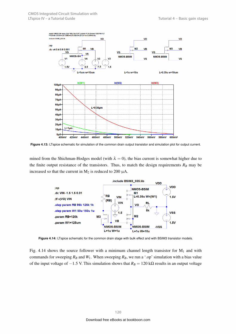
CMOS Integrated Circuit Simulation with LTspice IV – a Tutorial Guide
120
Tutorial 4 – Basic gain stagesCMOS Integrated Circuit Simulation with LTspice IV Tutorial 4
Figure 4.13: LTspice schematic for simulation of the common drain output transistor and simulation plot for output current.
mined from the Shichman-Hodges model (with λ = 0), the bias current is somewhat higher due tothe finite output resistance of the transistors. Thus, to match the design requirements RB may beincreased so that the current in M2 is reduced to 200 µA.
Figure 4.14: LTspice schematic for the common drain stage with bulk effect and with BSIM3 transistor models.
Fig. 4.14 shows the source follower with a minimum channel length transistor for M1 and withcommands for sweeping RB and W1. When sweeping RB, we run a ‘.op’ simulation with a bias valueof the input voltage of −1.5 V. This simulation shows that RB = 120 kΩ results in an output voltage
120
Download free eBooks at bookboon.com
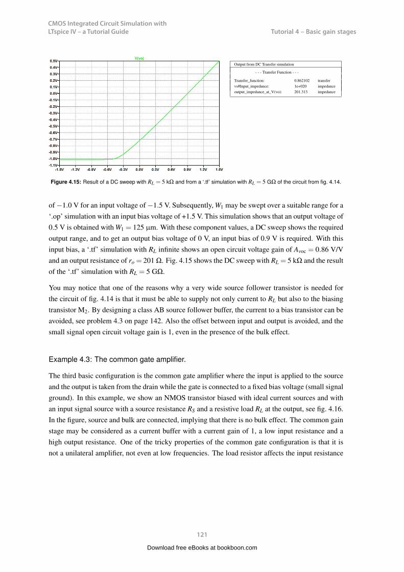
CMOS Integrated Circuit Simulation with LTspice IV – a Tutorial Guide
121
Tutorial 4 – Basic gain stagesCMOS Integrated Circuit Simulation with LTspice IV Tutorial 4
Output from DC Transfer simulation
- - - Transfer Function - - -
Transfer_function: 0.862102 transfervs#Input_impedance: 1e+020 impedanceoutput_impedance_at_V(vo): 201.313 impedance
Figure 4.15: Result of a DC sweep with RL = 5 kΩ and from a ‘.tf’ simulation with RL = 5 GΩ of the circuit from fig. 4.14.
of −1.0 V for an input voltage of −1.5 V. Subsequently, W1 may be swept over a suitable range for a‘.op’ simulation with an input bias voltage of +1.5 V. This simulation shows that an output voltage of0.5 V is obtained with W1 = 125 µm. With these component values, a DC sweep shows the requiredoutput range, and to get an output bias voltage of 0 V, an input bias of 0.9 V is required. With thisinput bias, a ‘.tf’ simulation with RL infinite shows an open circuit voltage gain of Avoc = 0.86 V/Vand an output resistance of ro = 201 Ω. Fig. 4.15 shows the DC sweep with RL = 5 kΩ and the resultof the ‘.tf’ simulation with RL = 5 GΩ.
You may notice that one of the reasons why a very wide source follower transistor is needed forthe circuit of fig. 4.14 is that it must be able to supply not only current to RL but also to the biasingtransistor M2. By designing a class AB source follower buffer, the current to a bias transistor can beavoided, see problem 4.3 on page 142. Also the offset between input and output is avoided, and thesmall signal open circuit voltage gain is 1, even in the presence of the bulk effect.
Example 4.3: The common gate amplifier.
The third basic configuration is the common gate amplifier where the input is applied to the sourceand the output is taken from the drain while the gate is connected to a fixed bias voltage (small signalground). In this example, we show an NMOS transistor biased with ideal current sources and withan input signal source with a source resistance RS and a resistive load RL at the output, see fig. 4.16.In the figure, source and bulk are connected, implying that there is no bulk effect. The common gainstage may be considered as a current buffer with a current gain of 1, a low input resistance and ahigh output resistance. One of the tricky properties of the common gate configuration is that it isnot a unilateral amplifier, not even at low frequencies. The load resistor affects the input resistance
121
Download free eBooks at bookboon.com

CMOS Integrated Circuit Simulation with LTspice IV – a Tutorial Guide
122
Tutorial 4 – Basic gain stagesCMOS Integrated Circuit Simulation with LTspice IV Tutorial 4
of the stage, and the source resistor affects the output resistance of the stage. From (Carusone,Johns & Martin 2012, p. 126) we have the following expressions for small signal voltage gain, inputresistance and output resistance:
Av =vo
vin=
(gm +gds)RL
1+RLgds +(gm +gds)RS(4.10)
rin =1+RLgds
gm +gds(4.11)
ro = 1/gds +RS(1+gm/gds) (4.12)
where gm is the transconductance and gds is the output conductance of the common gate transistor.If the common gate transistor has its bulk contact connected to a fixed voltage (e.g −VSS), gm shouldbe replaced by gm +gmb in these equations.
With RL → ∞, the input resistance approaches infinity, and with RS → ∞, the output resistanceapproaches infinity. The voltage gain approaches a maximum of 1+ gm/gds gm/gds for RS = 0and RL → ∞.
These relations may be illustrated from a simulation of the circuit which is shown as an LTspiceschematic in fig. 4.17. For the simulations, we are assuming a Shichman-Hodges transistor modeland transistor dimensions and bias currents as shown in the figure. In the schematic, both RL andRS are defined as parameters which can be swept in order to find the input resistance and the output
122
Download free eBooks at bookboon.com
Click on the ad to read moreClick on the ad to read moreClick on the ad to read moreClick on the ad to read moreClick on the ad to read moreClick on the ad to read moreClick on the ad to read moreClick on the ad to read moreClick on the ad to read moreClick on the ad to read moreClick on the ad to read moreClick on the ad to read moreClick on the ad to read moreClick on the ad to read moreClick on the ad to read moreClick on the ad to read moreClick on the ad to read moreClick on the ad to read moreClick on the ad to read moreClick on the ad to read moreClick on the ad to read moreClick on the ad to read moreClick on the ad to read moreClick on the ad to read moreClick on the ad to read moreClick on the ad to read moreClick on the ad to read moreClick on the ad to read moreClick on the ad to read moreClick on the ad to read moreClick on the ad to read moreClick on the ad to read moreClick on the ad to read moreClick on the ad to read moreClick on the ad to read moreClick on the ad to read moreClick on the ad to read moreClick on the ad to read moreClick on the ad to read moreClick on the ad to read moreClick on the ad to read moreClick on the ad to read more
© Deloitte & Touche LLP and affiliated entities.
360°thinking.
Discover the truth at www.deloitte.ca/careers
© Deloitte & Touche LLP and affiliated entities.
360°thinking.
Discover the truth at www.deloitte.ca/careers
© Deloitte & Touche LLP and affiliated entities.
360°thinking.
Discover the truth at www.deloitte.ca/careers © Deloitte & Touche LLP and affiliated entities.
360°thinking.
Discover the truth at www.deloitte.ca/careers
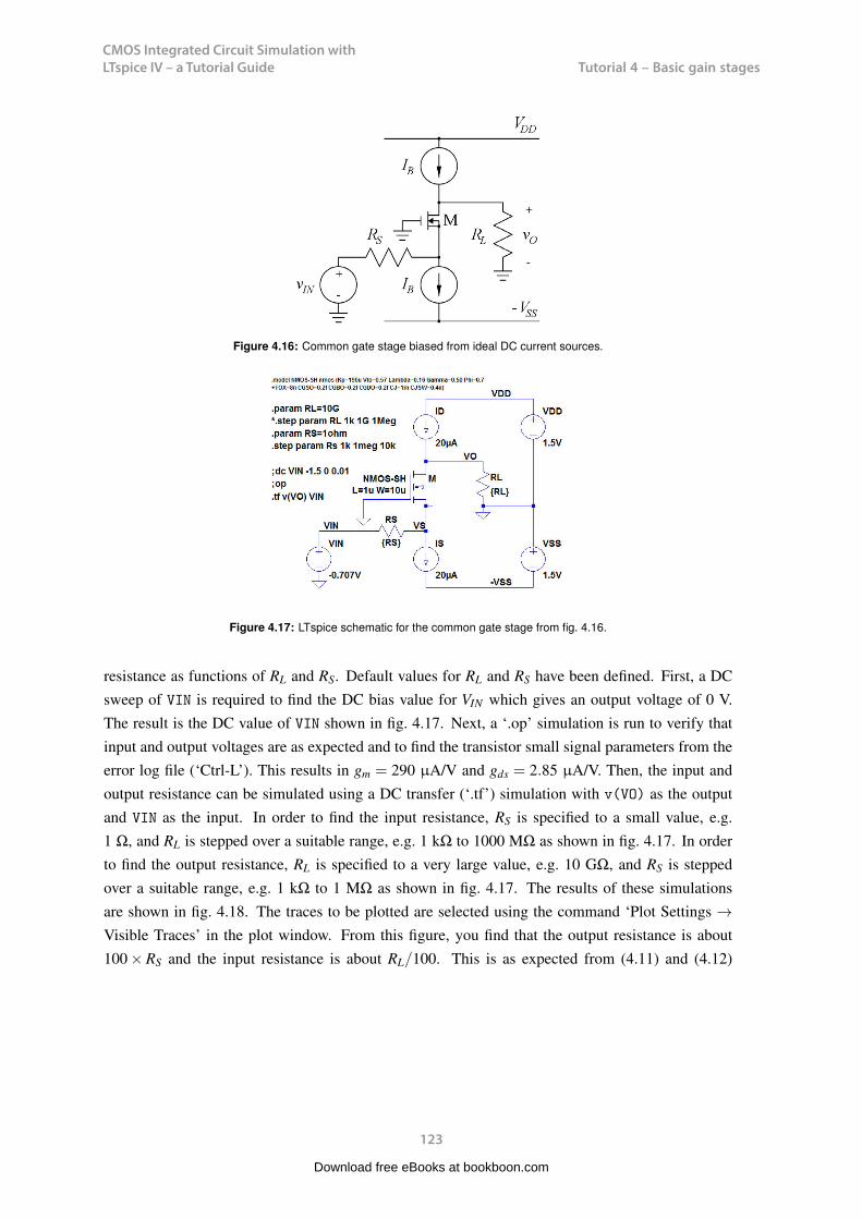
CMOS Integrated Circuit Simulation with LTspice IV – a Tutorial Guide
123
Tutorial 4 – Basic gain stagesCMOS Integrated Circuit Simulation with LTspice IV Tutorial 4
Figure 4.16: Common gate stage biased from ideal DC current sources.
Figure 4.17: LTspice schematic for the common gate stage from fig. 4.16.
resistance as functions of RL and RS. Default values for RL and RS have been defined. First, a DCsweep of VIN is required to find the DC bias value for VIN which gives an output voltage of 0 V.The result is the DC value of VIN shown in fig. 4.17. Next, a ‘.op’ simulation is run to verify thatinput and output voltages are as expected and to find the transistor small signal parameters from theerror log file (‘Ctrl-L’). This results in gm = 290 µA/V and gds = 2.85 µA/V. Then, the input andoutput resistance can be simulated using a DC transfer (‘.tf’) simulation with v(VO) as the outputand VIN as the input. In order to find the input resistance, RS is specified to a small value, e.g.1 Ω, and RL is stepped over a suitable range, e.g. 1 kΩ to 1000 MΩ as shown in fig. 4.17. In orderto find the output resistance, RL is specified to a very large value, e.g. 10 GΩ, and RS is steppedover a suitable range, e.g. 1 kΩ to 1 MΩ as shown in fig. 4.17. The results of these simulationsare shown in fig. 4.18. The traces to be plotted are selected using the command ‘Plot Settings →Visible Traces’ in the plot window. From this figure, you find that the output resistance is about100 × RS and the input resistance is about RL/100. This is as expected from (4.11) and (4.12)
123
Download free eBooks at bookboon.com
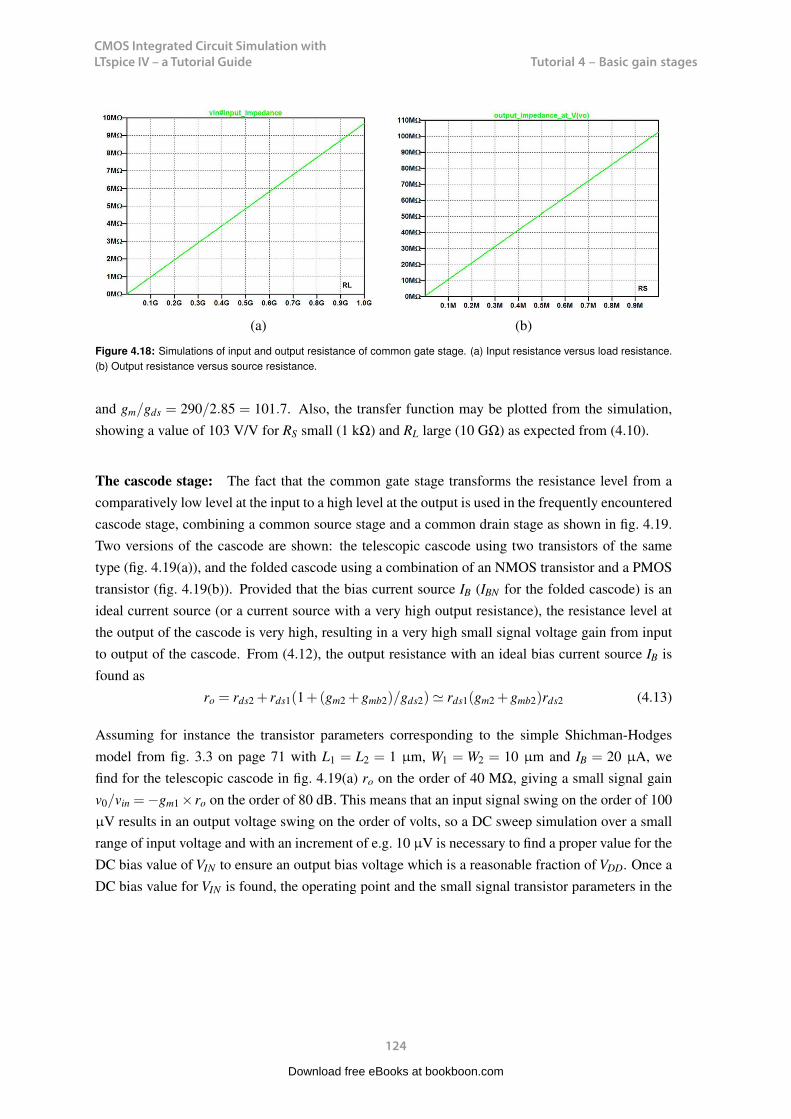
CMOS Integrated Circuit Simulation with LTspice IV – a Tutorial Guide
124
Tutorial 4 – Basic gain stagesCMOS Integrated Circuit Simulation with LTspice IV Tutorial 4
(a) (b)
Figure 4.18: Simulations of input and output resistance of common gate stage. (a) Input resistance versus load resistance.(b) Output resistance versus source resistance.
and gm/gds = 290/2.85 = 101.7. Also, the transfer function may be plotted from the simulation,showing a value of 103 V/V for RS small (1 kΩ) and RL large (10 GΩ) as expected from (4.10).
The cascode stage: The fact that the common gate stage transforms the resistance level from acomparatively low level at the input to a high level at the output is used in the frequently encounteredcascode stage, combining a common source stage and a common drain stage as shown in fig. 4.19.Two versions of the cascode are shown: the telescopic cascode using two transistors of the sametype (fig. 4.19(a)), and the folded cascode using a combination of an NMOS transistor and a PMOStransistor (fig. 4.19(b)). Provided that the bias current source IB (IBN for the folded cascode) is anideal current source (or a current source with a very high output resistance), the resistance level atthe output of the cascode is very high, resulting in a very high small signal voltage gain from inputto output of the cascode. From (4.12), the output resistance with an ideal bias current source IB isfound as
ro = rds2 + rds1(1+(gm2 +gmb2)/gds2) rds1(gm2 +gmb2)rds2 (4.13)
Assuming for instance the transistor parameters corresponding to the simple Shichman-Hodgesmodel from fig. 3.3 on page 71 with L1 = L2 = 1 µm, W1 = W2 = 10 µm and IB = 20 µA, wefind for the telescopic cascode in fig. 4.19(a) ro on the order of 40 MΩ, giving a small signal gainv0/vin =−gm1 × ro on the order of 80 dB. This means that an input signal swing on the order of 100µV results in an output voltage swing on the order of volts, so a DC sweep simulation over a smallrange of input voltage and with an increment of e.g. 10 µV is necessary to find a proper value for theDC bias value of VIN to ensure an output bias voltage which is a reasonable fraction of VDD. Once aDC bias value for VIN is found, the operating point and the small signal transistor parameters in the
124
Download free eBooks at bookboon.com

CMOS Integrated Circuit Simulation with LTspice IV – a Tutorial Guide
125
Tutorial 4 – Basic gain stagesCMOS Integrated Circuit Simulation with LTspice IV Tutorial 4
(a) (b)
Figure 4.19: Cascode stage. (a) Telescopic cascode. (b) Folded cascode.
operating point can be found from a ‘.op’ simulation, and gain and output resistance can be foundfrom a ‘.tf’ simulation. Also the resistance level in the intermediate node x can be found from a ‘.tf’simulation with V(vx) defined as the output. The detailed simulations for the circuits from fig. 4.19are left for the reader, see problems 4.4 and 4.5 on page 143 and 144.
125
Download free eBooks at bookboon.com
Click on the ad to read moreClick on the ad to read moreClick on the ad to read moreClick on the ad to read moreClick on the ad to read moreClick on the ad to read moreClick on the ad to read moreClick on the ad to read moreClick on the ad to read moreClick on the ad to read moreClick on the ad to read moreClick on the ad to read moreClick on the ad to read moreClick on the ad to read moreClick on the ad to read moreClick on the ad to read moreClick on the ad to read moreClick on the ad to read moreClick on the ad to read moreClick on the ad to read moreClick on the ad to read moreClick on the ad to read moreClick on the ad to read moreClick on the ad to read moreClick on the ad to read moreClick on the ad to read moreClick on the ad to read moreClick on the ad to read moreClick on the ad to read moreClick on the ad to read moreClick on the ad to read moreClick on the ad to read moreClick on the ad to read moreClick on the ad to read moreClick on the ad to read moreClick on the ad to read moreClick on the ad to read moreClick on the ad to read moreClick on the ad to read moreClick on the ad to read moreClick on the ad to read moreClick on the ad to read moreClick on the ad to read more
We will turn your CV into an opportunity of a lifetime
Do you like cars? Would you like to be a part of a successful brand?We will appreciate and reward both your enthusiasm and talent.Send us your CV. You will be surprised where it can take you.
Send us your CV onwww.employerforlife.com
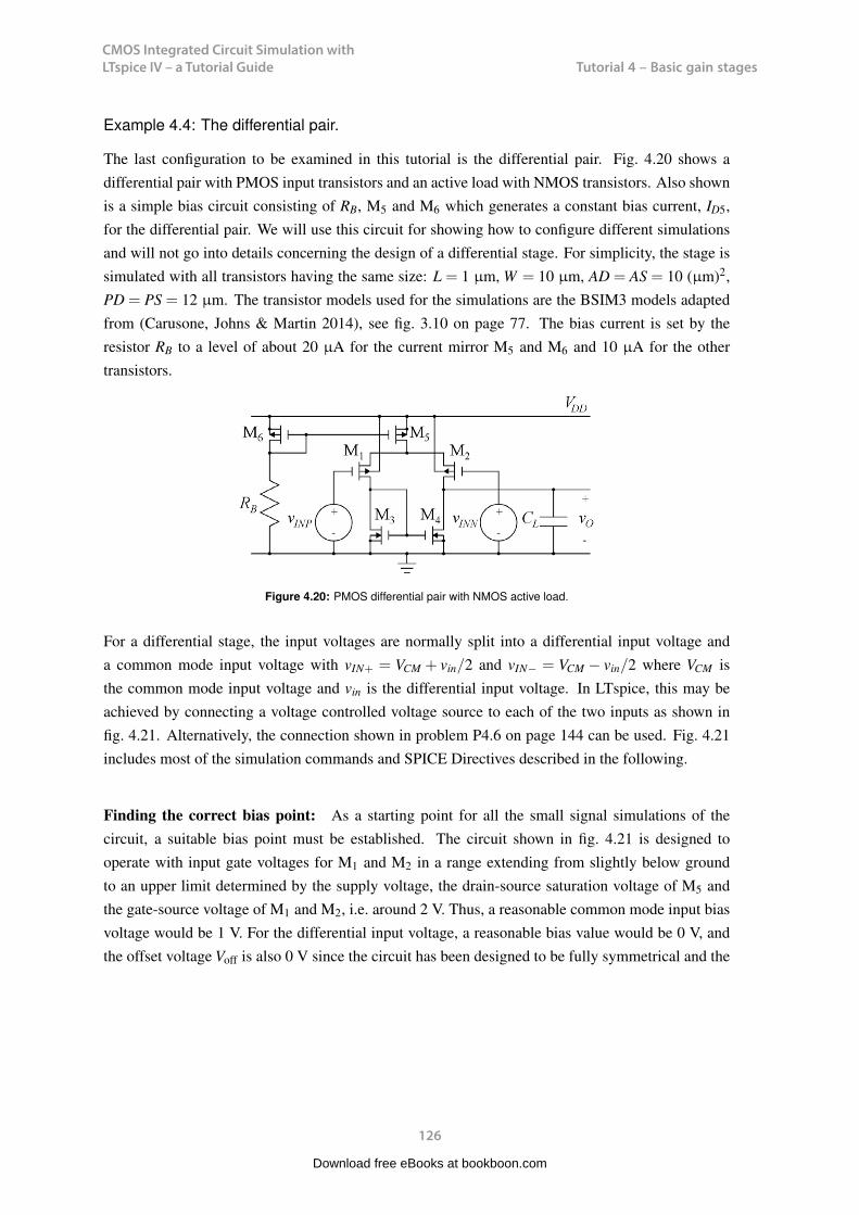
CMOS Integrated Circuit Simulation with LTspice IV – a Tutorial Guide
126
Tutorial 4 – Basic gain stagesCMOS Integrated Circuit Simulation with LTspice IV Tutorial 4
Example 4.4: The differential pair.
The last configuration to be examined in this tutorial is the differential pair. Fig. 4.20 shows adifferential pair with PMOS input transistors and an active load with NMOS transistors. Also shownis a simple bias circuit consisting of RB, M5 and M6 which generates a constant bias current, ID5,for the differential pair. We will use this circuit for showing how to configure different simulationsand will not go into details concerning the design of a differential stage. For simplicity, the stage issimulated with all transistors having the same size: L = 1 µm, W = 10 µm, AD = AS = 10 (µm)2,PD = PS = 12 µm. The transistor models used for the simulations are the BSIM3 models adaptedfrom (Carusone, Johns & Martin 2014), see fig. 3.10 on page 77. The bias current is set by theresistor RB to a level of about 20 µA for the current mirror M5 and M6 and 10 µA for the othertransistors.
Figure 4.20: PMOS differential pair with NMOS active load.
For a differential stage, the input voltages are normally split into a differential input voltage anda common mode input voltage with vIN+ = VCM + vin/2 and vIN− = VCM − vin/2 where VCM isthe common mode input voltage and vin is the differential input voltage. In LTspice, this may beachieved by connecting a voltage controlled voltage source to each of the two inputs as shown infig. 4.21. Alternatively, the connection shown in problem P4.6 on page 144 can be used. Fig. 4.21includes most of the simulation commands and SPICE Directives described in the following.
Finding the correct bias point: As a starting point for all the small signal simulations of thecircuit, a suitable bias point must be established. The circuit shown in fig. 4.21 is designed tooperate with input gate voltages for M1 and M2 in a range extending from slightly below groundto an upper limit determined by the supply voltage, the drain-source saturation voltage of M5 andthe gate-source voltage of M1 and M2, i.e. around 2 V. Thus, a reasonable common mode input biasvoltage would be 1 V. For the differential input voltage, a reasonable bias value would be 0 V, andthe offset voltage Voff is also 0 V since the circuit has been designed to be fully symmetrical and the
126
Download free eBooks at bookboon.com
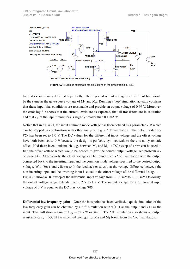
CMOS Integrated Circuit Simulation with LTspice IV – a Tutorial Guide
127
Tutorial 4 – Basic gain stagesCMOS Integrated Circuit Simulation with LTspice IV Tutorial 4
Figure 4.21: LTspice schematic for simulations of the circuit from fig. 4.20.
transistors are assumed to match perfectly. The expected output voltage for this input bias wouldbe the same as the gate-source voltage of M3 and M4. Running a ‘.op’ simulation actually confirmsthat these input bias conditions are reasonable and provide an output voltage of 0.69 V. Moreover,the error log file shows that the current levels are as expected, that all transistors are in saturationand that gm of the input transistors is slightly smaller than 0.1 mA/V.
Notice that in fig. 4.21, the input common mode voltage has been defined as a parameter VCM whichcan be stepped in combination with other analyses, e.g. a ‘.tf’ simulation. The default value forVCM has been set to 1.0 V. The DC values for the differential input voltage and the offset voltagehave both been set to 0 V because the design is perfectly symmetrical, so there is no systematicoffset. Had there been a mismatch, e.g. between M1 and M2, a DC sweep of Voff can be used tofind the offset voltage which would be needed to give the correct output voltage, see problem 4.7on page 145. Alternatively, the offset voltage can be found from a ‘.op’ simulation with the outputconnected back to the inverting input and the common mode voltage specified to the desired outputvoltage. With Voff and VID set to 0, the feedback ensures that the voltage difference between thenon-inverting input and the inverting input is equal to the offset voltage of the differential stage.Fig. 4.22 shows a DC sweep of the differential input voltage from −100 mV to +100 mV. Obviously,the output voltage range extends from 0.2 V to 1.8 V. The output voltage for a differential inputvoltage of 0 V is equal to the DC bias voltage VG3.
Differential low frequency gain: Once the bias point has been verified, a quick simulation of thelow frequency gain can be obtained by a ‘.tf’ simulation with v(VO) as the output and VID as theinput. This will show a gain of Avoc = 52 V/V or 34 dB. The ‘.tf’ simulation also shows an output
127
CMOS Integrated Circuit Simulation with LTspice IV Tutorial 4
Figure 4.22: Plot of output voltage versus differential input voltage for a common mode input voltage of 1 V for the circuit offig. 4.21.
resistance of ro = 535 kΩ as expected from gds for M2 and M4 found from the ‘.op’ simulation.
Input common mode voltage range: The input common mode range is the voltage range for VCM
where the differential stage has all transistors operating in the active region so that the small signalgain is almost constant over this range of VCM. For the circuit of fig. 4.20, the upper limit is definedby M5 which enters the triode region when VCM increases, implying that M5 can no longer supply
128
Download free eBooks at bookboon.com

CMOS Integrated Circuit Simulation with LTspice IV – a Tutorial Guide
128
Tutorial 4 – Basic gain stagesCMOS Integrated Circuit Simulation with LTspice IV Tutorial 4
Figure 4.22: Plot of output voltage versus differential input voltage for a common mode input voltage of 1 V for the circuit offig. 4.21.
resistance of ro = 535 kΩ as expected from gds for M2 and M4 found from the ‘.op’ simulation.
Input common mode voltage range: The input common mode range is the voltage range for VCM
where the differential stage has all transistors operating in the active region so that the small signalgain is almost constant over this range of VCM. For the circuit of fig. 4.20, the upper limit is definedby M5 which enters the triode region when VCM increases, implying that M5 can no longer supply
128
CMOS Integrated Circuit Simulation with LTspice IV Tutorial 4
Figure 4.22: Plot of output voltage versus differential input voltage for a common mode input voltage of 1 V for the circuit offig. 4.21.
resistance of ro = 535 kΩ as expected from gds for M2 and M4 found from the ‘.op’ simulation.
Input common mode voltage range: The input common mode range is the voltage range for VCM
where the differential stage has all transistors operating in the active region so that the small signalgain is almost constant over this range of VCM. For the circuit of fig. 4.20, the upper limit is definedby M5 which enters the triode region when VCM increases, implying that M5 can no longer supply
128
Download free eBooks at bookboon.com
Click on the ad to read moreClick on the ad to read moreClick on the ad to read moreClick on the ad to read moreClick on the ad to read moreClick on the ad to read moreClick on the ad to read moreClick on the ad to read moreClick on the ad to read moreClick on the ad to read moreClick on the ad to read moreClick on the ad to read moreClick on the ad to read moreClick on the ad to read moreClick on the ad to read moreClick on the ad to read moreClick on the ad to read moreClick on the ad to read moreClick on the ad to read moreClick on the ad to read moreClick on the ad to read moreClick on the ad to read moreClick on the ad to read moreClick on the ad to read moreClick on the ad to read moreClick on the ad to read moreClick on the ad to read moreClick on the ad to read moreClick on the ad to read moreClick on the ad to read moreClick on the ad to read moreClick on the ad to read moreClick on the ad to read moreClick on the ad to read moreClick on the ad to read moreClick on the ad to read moreClick on the ad to read moreClick on the ad to read moreClick on the ad to read moreClick on the ad to read moreClick on the ad to read moreClick on the ad to read moreClick on the ad to read moreClick on the ad to read more
Maersk.com/Mitas
e Graduate Programme for Engineers and Geoscientists
Month 16I was a construction
supervisor in the North Sea
advising and helping foremen
solve problems
I was a
hes
Real work International opportunities
ree work placementsal Internationaorree wo
I wanted real responsibili I joined MITAS because
www.discovermitas.com
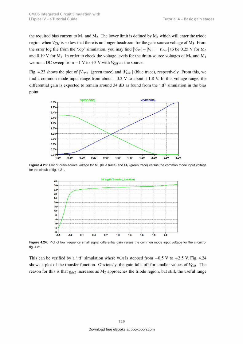
CMOS Integrated Circuit Simulation with LTspice IV – a Tutorial Guide
129
Tutorial 4 – Basic gain stagesCMOS Integrated Circuit Simulation with LTspice IV Tutorial 4
the required bias current to M1 and M2. The lower limit is defined by M1 which will enter the trioderegion when VCM is so low that there is no longer headroom for the gate-source voltage of M3. Fromthe error log file from the ‘.op’ simulation, you may find |VGS|− |Vt | = |Vdsat | to be 0.25 V for M5
and 0.19 V for M1. In order to check the voltage levels for the drain-source voltages of M5 and M1
we run a DC sweep from −1 V to +3 V with VCM as the source.
Fig. 4.23 shows the plot of |VDS5| (green trace) and |VDS1| (blue trace), respectively. From this, wefind a common mode input range from about −0.2 V to about +1.8 V. In this voltage range, thedifferential gain is expected to remain around 34 dB as found from the ‘.tf’ simulation in the biaspoint.
Figure 4.23: Plot of drain-source voltage for M1 (blue trace) and M5 (green trace) versus the common mode input voltagefor the circuit of fig. 4.21.
Figure 4.24: Plot of low frequency small signal differential gain versus the common mode input voltage for the circuit offig. 4.21.
This can be verified by a ‘.tf’ simulation where VCM is stepped from −0.5 V to +2.5 V. Fig. 4.24shows a plot of the transfer function. Obviously, the gain falls off for smaller values of VCM. Thereason for this is that gds2 increases as M2 approaches the triode region, but still, the useful range
129
Download free eBooks at bookboon.com

CMOS Integrated Circuit Simulation with LTspice IV – a Tutorial Guide
130
Tutorial 4 – Basic gain stagesCMOS Integrated Circuit Simulation with LTspice IV Tutorial 4
extends down to the negative rail with a drop in gain of less than 3 dB. You may introduce a smallnegative offset voltage (e.g. −5 mV) to reduce the bias value of the output voltage and thus bringM2 deeper into the active region. With Voff =−5 mV you will find a gain of more than 31 dB for acommon mode input voltage down to −0.22 V.
For VCM in the range from 1.8 V to 2.5 V, the gain increases somewhat. The reason for this is thatM5 enters the triode region, so the bias current for the differential pair is reduced, leading to smallervalues of gm and gds with gds being reduced more than gm. This range of operation will normally notbe considered as useful because the smaller bias current also means smaller slew rate and smallerunity gain frequency.
Differential frequency response: When the differential stage is loaded by a capacitance CL whichis much larger than the internal transistor capacitances, the frequency response is expected to have adominant pole at ωp = (roCL)
−1 and a gain bandwidth product of 2π ×GBW = Avocωp = gm1/CL.From the error log file from a ‘.op’ simulation, we see that the internal transistor capacitances areon the order of 10−14 F, i.e. more than one order of magnitude smaller than CL, so the condition fora dominant pole is fulfilled, but non-dominant poles can be expected at frequencies comparable tothe gain bandwidth product. An AC simulation with Vid as the input signal results in a Bode plotfor the output voltage as shown in fig. 4.25. Vid is defined as the input signal by specifying the AC
130
Download free eBooks at bookboon.com
Click on the ad to read moreClick on the ad to read moreClick on the ad to read moreClick on the ad to read moreClick on the ad to read moreClick on the ad to read moreClick on the ad to read moreClick on the ad to read moreClick on the ad to read moreClick on the ad to read moreClick on the ad to read moreClick on the ad to read moreClick on the ad to read moreClick on the ad to read moreClick on the ad to read moreClick on the ad to read moreClick on the ad to read moreClick on the ad to read moreClick on the ad to read moreClick on the ad to read moreClick on the ad to read moreClick on the ad to read moreClick on the ad to read moreClick on the ad to read moreClick on the ad to read moreClick on the ad to read moreClick on the ad to read moreClick on the ad to read moreClick on the ad to read moreClick on the ad to read moreClick on the ad to read moreClick on the ad to read moreClick on the ad to read moreClick on the ad to read moreClick on the ad to read moreClick on the ad to read moreClick on the ad to read moreClick on the ad to read moreClick on the ad to read moreClick on the ad to read moreClick on the ad to read moreClick on the ad to read moreClick on the ad to read moreClick on the ad to read moreClick on the ad to read more
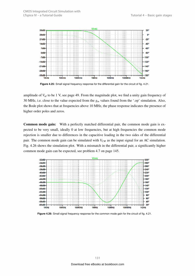
CMOS Integrated Circuit Simulation with LTspice IV – a Tutorial Guide
131
Tutorial 4 – Basic gain stagesCMOS Integrated Circuit Simulation with LTspice IV Tutorial 4
Figure 4.25: Small signal frequency response for the differential gain for the circuit of fig. 4.21.
amplitude of Vid to be 1 V, see page 49. From the magnitude plot, we find a unity gain frequency of30 MHz, i.e. close to the value expected from the gm values found from the ‘.op’ simulation. Also,the Bode plot shows that at frequencies above 10 MHz, the phase response indicates the presence ofhigher order poles and zeros.
Common mode gain: With a perfectly matched differential pair, the common mode gain is ex-pected to be very small, ideally 0 at low frequencies, but at high frequencies the common moderejection is smaller due to differences in the capacitive loading in the two sides of the differentialpair. The common mode gain can be simulated with VCM as the input signal for an AC simulation.Fig. 4.26 shows the simulation plot. With a mismatch in the differential pair, a significantly highercommon mode gain can be expected, see problem 4.7 on page 145.
Figure 4.26: Small signal frequency response for the common mode gain for the circuit of fig. 4.21.
131
Download free eBooks at bookboon.com
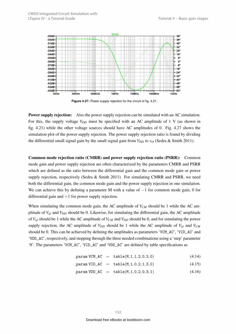
CMOS Integrated Circuit Simulation with LTspice IV – a Tutorial Guide
132
Tutorial 4 – Basic gain stagesCMOS Integrated Circuit Simulation with LTspice IV Tutorial 4
Figure 4.27: Power supply rejection for the circuit of fig. 4.21.
Power supply rejection: Also the power supply rejection can be simulated with an AC simulation.For this, the supply voltage VDD must be specified with an AC amplitude of 1 V (as shown infig. 4.21) while the other voltage sources should have AC amplitudes of 0. Fig. 4.27 shows thesimulation plot of the power supply rejection. The power supply rejection ratio is found by dividingthe differential small signal gain by the small signal gain from VDD to vO (Sedra & Smith 2011).
Common mode rejection ratio (CMRR) and power supply rejection ratio (PSRR): Commonmode gain and power supply rejection are often characterized by the parameters CMRR and PSRRwhich are defined as the ratio between the differential gain and the common mode gain or powersupply rejection, respectively (Sedra & Smith 2011). For simulating CMRR and PSRR, we needboth the differential gain, the common mode gain and the power supply rejection in one simulation.We can achieve this by defining a parameter M with a value of −1 for common mode gain, 0 fordifferential gain and +1 for power supply rejection.
When simulating the common mode gain, the AC amplitude of VCM should be 1 while the AC am-plitude of Vid and VDD should be 0. Likewise, for simulating the differential gain, the AC amplitudeof Vid should be 1 while the AC amplitude of VCM and VDD should be 0, and for simulating the powersupply rejection, the AC amplitude of VDD should be 1 while the AC amplitude of Vid and VCM
should be 0. This can be achieved by defining the amplitudes as parameters ‘VCM_AC’, ‘VID_AC’ and‘VDD_AC’, respectively, and stepping through the three needed combinations using a ‘step’ parameter‘M’. The parameters ‘VCM_AC’, ‘VID_AC’ and ‘VDD_AC’ are defined by table specifications as
.param VCM_AC = table(M,1,1,2,0,3,0) (4.14)
.param VID_AC = table(M,1,0,2,1,3,0) (4.15)
132
CMOS Integrated Circuit Simulation with LTspice IV Tutorial 4
.param VDD_AC = table(M,1,0,2,0,3,1) (4.16)
In (4.14) - (4.16), the first table entry is the step number M, and this is followed by pairs of M-values(counting from 1 to 3) and amplitude values.
Fig. 4.28 shows the LTspice schematic with these definitions of the AC amplitudes and the ‘.ac’simulation command. Also included is the ‘.step’ command, stepping M through the values 1, 2 and3 in order to achieve the common mode gain, the differential gain and the power supply rejection inone simulation.
Figure 4.28: LTspice schematic for simulating both common mode gain, differential gain and power supply rejection.
Figure 4.29: Common mode gain (green trace), differential gain (blue trace) and power supply rejection (red trace) for thecircuit of fig. 4.21.
133
Download free eBooks at bookboon.com
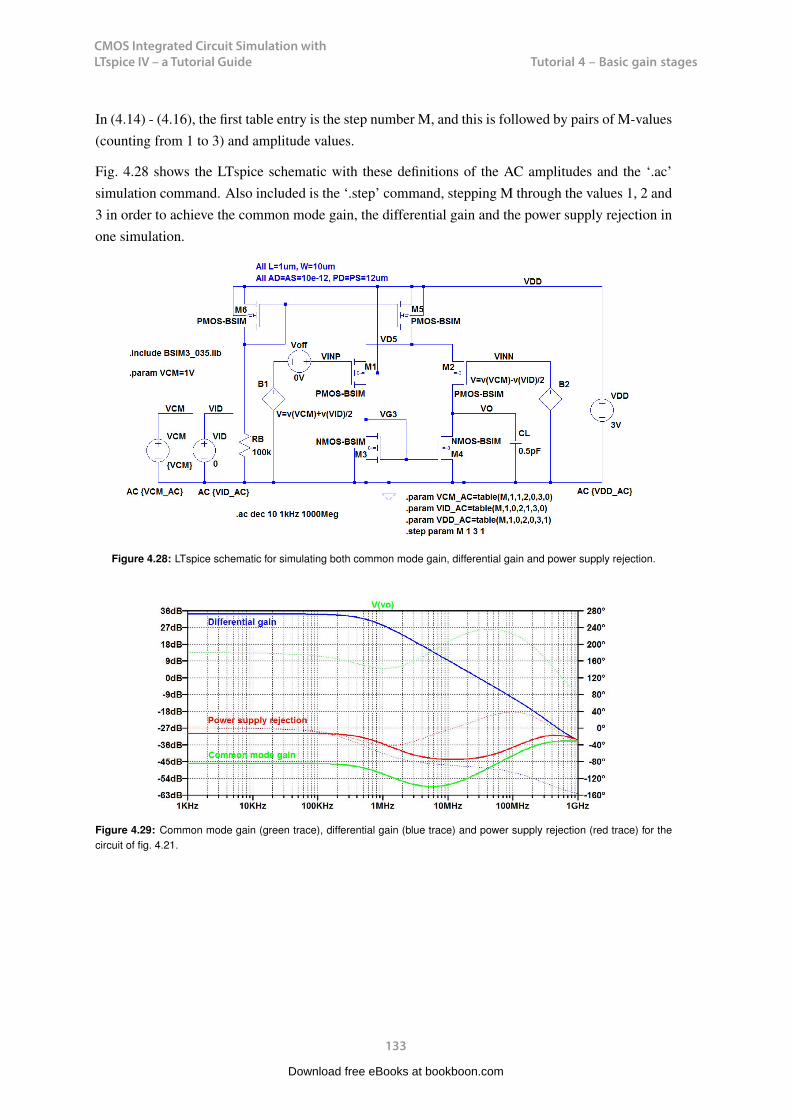
CMOS Integrated Circuit Simulation with LTspice IV – a Tutorial Guide
133
Tutorial 4 – Basic gain stages
CMOS Integrated Circuit Simulation with LTspice IV Tutorial 4
.param VDD_AC = table(M,1,0,2,0,3,1) (4.16)
In (4.14) - (4.16), the first table entry is the step number M, and this is followed by pairs of M-values(counting from 1 to 3) and amplitude values.
Fig. 4.28 shows the LTspice schematic with these definitions of the AC amplitudes and the ‘.ac’simulation command. Also included is the ‘.step’ command, stepping M through the values 1, 2 and3 in order to achieve the common mode gain, the differential gain and the power supply rejection inone simulation.
Figure 4.28: LTspice schematic for simulating both common mode gain, differential gain and power supply rejection.
Figure 4.29: Common mode gain (green trace), differential gain (blue trace) and power supply rejection (red trace) for thecircuit of fig. 4.21.
133
Download free eBooks at bookboon.com
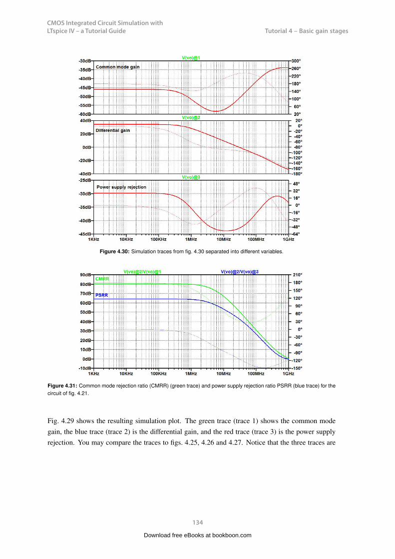
CMOS Integrated Circuit Simulation with LTspice IV – a Tutorial Guide
134
Tutorial 4 – Basic gain stagesCMOS Integrated Circuit Simulation with LTspice IV Tutorial 4
Figure 4.30: Simulation traces from fig. 4.30 separated into different variables.
Figure 4.31: Common mode rejection ratio (CMRR) (green trace) and power supply rejection ratio PSRR (blue trace) for thecircuit of fig. 4.21.
Fig. 4.29 shows the resulting simulation plot. The green trace (trace 1) shows the common modegain, the blue trace (trace 2) is the differential gain, and the red trace (trace 3) is the power supplyrejection. You may compare the traces to figs. 4.25, 4.26 and 4.27. Notice that the three traces are
134
Download free eBooks at bookboon.com

CMOS Integrated Circuit Simulation with LTspice IV – a Tutorial Guide
135
Tutorial 4 – Basic gain stagesCMOS Integrated Circuit Simulation with LTspice IV Tutorial 4
plotted as the result of showing just one variable, ‘V(vo)’. For finding CMRR and PSRR, we needto separate the three traces into different variables. This is achieved by adding the operand @ to thevariable. Thus, ‘V(vo)@1’ shows only the common mode gain (trace 1), ‘V(vo)@2’ shows only thedifferential gain (trace 2), and ‘V(vo)@3’ shows only the power supply rejection (trace 3). Fig. 4.30shows the three different traces in separate plot panes (achieved by the command ‘Plot Settings →Add Plot Pane’) so that different scaling of the Y-axes can be used.
Finally, fig. 4.31 shows CMRR and PSRR calculated as ‘V(vo)@2/V(vo)@1’ and ‘V(vo)@2/V(vo)@3’,respectively.
Slew rate: The slew rate SR of the output voltage is limited by the current I available to charge anddischarge the load capacitor CL. From SR = I/CL and with a maximum current I limited by M5, aslew rate of about 40 V/µs can be expected. The slew rate can be simulated by a transient simulationwith square wave pulses applied to the input, so that the output switches between the minimum andmaximum available output. Fig. 4.32 shows the simulation plot from a transient simulation. The plotshows the differential input voltage and the output voltage. From the slope of the output voltage, aslew rate of about 40 V/µs is found as expected with I = 20 µA and CL = 0.5 pF.
135
Download free eBooks at bookboon.com
Click on the ad to read moreClick on the ad to read moreClick on the ad to read moreClick on the ad to read moreClick on the ad to read moreClick on the ad to read moreClick on the ad to read moreClick on the ad to read moreClick on the ad to read moreClick on the ad to read moreClick on the ad to read moreClick on the ad to read moreClick on the ad to read moreClick on the ad to read moreClick on the ad to read moreClick on the ad to read moreClick on the ad to read moreClick on the ad to read moreClick on the ad to read moreClick on the ad to read moreClick on the ad to read moreClick on the ad to read moreClick on the ad to read moreClick on the ad to read moreClick on the ad to read moreClick on the ad to read moreClick on the ad to read moreClick on the ad to read moreClick on the ad to read moreClick on the ad to read moreClick on the ad to read moreClick on the ad to read moreClick on the ad to read moreClick on the ad to read moreClick on the ad to read moreClick on the ad to read moreClick on the ad to read moreClick on the ad to read moreClick on the ad to read moreClick on the ad to read moreClick on the ad to read moreClick on the ad to read moreClick on the ad to read moreClick on the ad to read moreClick on the ad to read moreClick on the ad to read more
STUDY AT A TOP RANKED INTERNATIONAL BUSINESS SCHOOL
Reach your full potential at the Stockholm School of Economics, in one of the most innovative cities in the world. The School is ranked by the Financial Times as the number one business school in the Nordic and Baltic countries.
Visit us at www.hhs.se
Swed
en
Stockholm
no.1nine years in a row
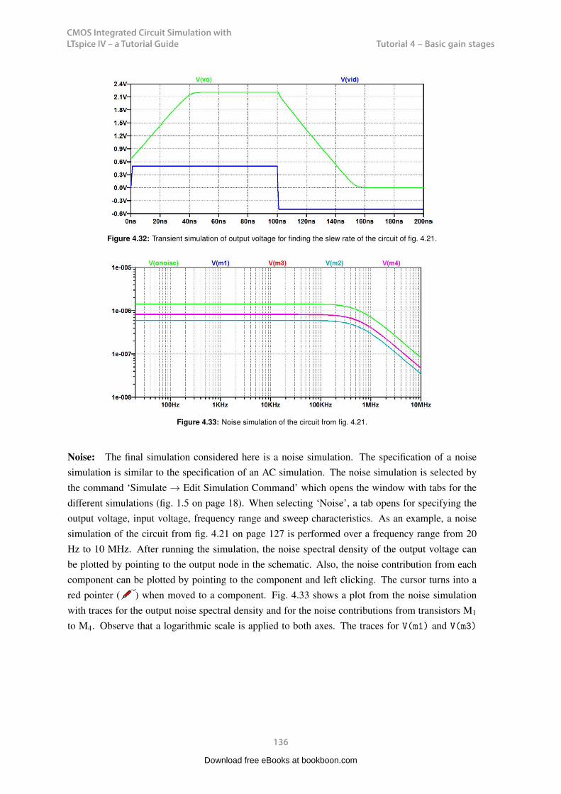
CMOS Integrated Circuit Simulation with LTspice IV – a Tutorial Guide
136
Tutorial 4 – Basic gain stagesCMOS Integrated Circuit Simulation with LTspice IV Tutorial 4
Figure 4.32: Transient simulation of output voltage for finding the slew rate of the circuit of fig. 4.21.
Figure 4.33: Noise simulation of the circuit from fig. 4.21.
Noise: The final simulation considered here is a noise simulation. The specification of a noisesimulation is similar to the specification of an AC simulation. The noise simulation is selected bythe command ‘Simulate → Edit Simulation Command’ which opens the window with tabs for thedifferent simulations (fig. 1.5 on page 18). When selecting ‘Noise’, a tab opens for specifying theoutput voltage, input voltage, frequency range and sweep characteristics. As an example, a noisesimulation of the circuit from fig. 4.21 on page 127 is performed over a frequency range from 20Hz to 10 MHz. After running the simulation, the noise spectral density of the output voltage canbe plotted by pointing to the output node in the schematic. Also, the noise contribution from eachcomponent can be plotted by pointing to the component and left clicking. The cursor turns into ared pointer ( ) when moved to a component. Fig. 4.33 shows a plot from the noise simulationwith traces for the output noise spectral density and for the noise contributions from transistors M1
to M4. Observe that a logarithmic scale is applied to both axes. The traces for V(m1) and V(m3)
136
Download free eBooks at bookboon.com

CMOS Integrated Circuit Simulation with LTspice IV – a Tutorial Guide
137
Tutorial 4 – Basic gain stagesCMOS Integrated Circuit Simulation with LTspice IV Tutorial 4
(noise from M1 and M3) cannot be seen as they are hidden beneath the identical noise contributionsfrom M2 and M4. All the noise contributions are noise at the specified output terminal. Obviously,for the circuit of fig. 4.21, the active load (M3 and M4) is the main noise contributor. It should benoted that the circuit of fig. 4.21 is in no way optimized for noise performance. For details on howto optimize this, the analysis from (Carusone, Johns & Martin 2012, pp. 392-394) may be applied.
A useful feature is that by pointing to a trace label and using ‘Ctrl-left click’, the total noise voltageintegrated over the specified frequency range is calculated and displayed in a separate window. Thus,for the circuit of fig. 4.21, a ‘Ctrl-left click’ on the trace label shows a total output noise RMS voltageof 1.33 mV.
Also the input referred spectral noise density may be plotted. It is selected from the schematic usingthe command ‘View → Visible Traces’ and selecting ‘V(inoise)’.
Note that the transistor models used for this simulation do not include flicker noise. This is apparentsince the noise spectral density is flat all the way down to very low frequencies. The noise parame-ters for a transistor may be included in the transistor model, but for the model taken from (Carusone,Johns & Martin 2014), no flicker noise parameters are specified. The most important parameterdescribing the flicker noise is the flicker noise coefficient KF (Baker 2010; Allen 2012). The mod-eling of flicker noise is beyond the scope of this tutorial. Problem 4.8 on page 145 illustrates thesimulation of flicker noise with noise parameters for a 0.35 µm CMOS process.
137
Download free eBooks at bookboon.com
Click on the ad to read moreClick on the ad to read moreClick on the ad to read moreClick on the ad to read moreClick on the ad to read moreClick on the ad to read moreClick on the ad to read moreClick on the ad to read moreClick on the ad to read moreClick on the ad to read moreClick on the ad to read moreClick on the ad to read moreClick on the ad to read moreClick on the ad to read moreClick on the ad to read moreClick on the ad to read moreClick on the ad to read moreClick on the ad to read moreClick on the ad to read moreClick on the ad to read moreClick on the ad to read moreClick on the ad to read moreClick on the ad to read moreClick on the ad to read moreClick on the ad to read moreClick on the ad to read moreClick on the ad to read moreClick on the ad to read moreClick on the ad to read moreClick on the ad to read moreClick on the ad to read moreClick on the ad to read moreClick on the ad to read moreClick on the ad to read moreClick on the ad to read moreClick on the ad to read moreClick on the ad to read moreClick on the ad to read moreClick on the ad to read moreClick on the ad to read moreClick on the ad to read moreClick on the ad to read moreClick on the ad to read moreClick on the ad to read moreClick on the ad to read moreClick on the ad to read moreClick on the ad to read more
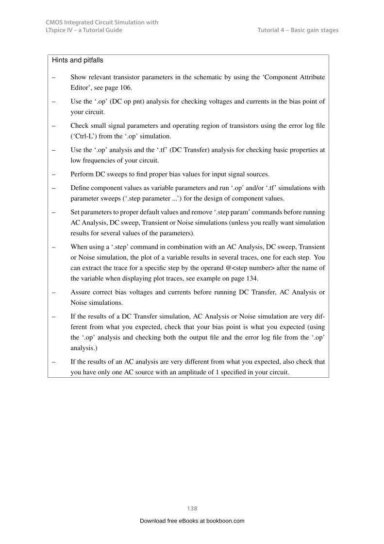
CMOS Integrated Circuit Simulation with LTspice IV – a Tutorial Guide
138
Tutorial 4 – Basic gain stagesCMOS Integrated Circuit Simulation with LTspice IV Tutorial 4
Hints and pitfalls
– Show relevant transistor parameters in the schematic by using the ‘Component AttributeEditor’, see page 106.
– Use the ‘.op’ (DC op pnt) analysis for checking voltages and currents in the bias point ofyour circuit.
– Check small signal parameters and operating region of transistors using the error log file(‘Ctrl-L’) from the ‘.op’ simulation.
– Use the ‘.op’ analysis and the ‘.tf’ (DC Transfer) analysis for checking basic properties atlow frequencies of your circuit.
– Perform DC sweeps to find proper bias values for input signal sources.
– Define component values as variable parameters and run ‘.op’ and/or ‘.tf’ simulations withparameter sweeps (‘.step parameter ...’) for the design of component values.
– Set parameters to proper default values and remove ‘.step param’ commands before runningAC Analysis, DC sweep, Transient or Noise simulations (unless you really want simulationresults for several values of the parameters).
– When using a ‘.step’ command in combination with an AC Analysis, DC sweep, Transientor Noise simulation, the plot of a variable results in several traces, one for each step. Youcan extract the trace for a specific step by the operand @<step number> after the name ofthe variable when displaying plot traces, see example on page 134.
– Assure correct bias voltages and currents before running DC Transfer, AC Analysis orNoise simulations.
– If the results of a DC Transfer simulation, AC Analysis or Noise simulation are very dif-ferent from what you expected, check that your bias point is what you expected (usingthe ‘.op’ analysis and checking both the output file and the error log file from the ‘.op’analysis.)
– If the results of an AC analysis are very different from what you expected, also check thatyou have only one AC source with an amplitude of 1 specified in your circuit.
138
Download free eBooks at bookboon.com

CMOS Integrated Circuit Simulation with LTspice IV – a Tutorial Guide
139
Tutorial 4 – Basic gain stagesCMOS Integrated Circuit Simulation with LTspice IV Tutorial 4
References
Allen, PE., & Holberg, DR. 2012, CMOS Analog Integrated Circuit Design, Third Edition, OxfordUniversity Press, New York, USA.
Baker, RJ. 2010, CMOS Circuit Design, Layout and Simulation, Third Edition, IEEE Press, Piscat-away, USA.
Carusone, TC., Johns, D. & Martin, K. 2012, Analog Integrated Circuit Design, Second Edition,John Wiley & Sons, Inc., Hoboken, USA.
Carusone, TC., Johns, D. & Martin, K. 2014, Analog Integrated Circuit Design, Netlist and modelfiles. Retrieved from http://analogicdesign.com/students/netlists-models/
Sedra, AS. & Smith, KC. 2011, Microelectronic Circuits, International Sixth Edition, Oxford Uni-versity Press, New York, USA.
Shichman, H. & Hodges, DA. 1968, ‘Modeling and Simulation of Insulated-Gate Field-Effect Tran-sistor Switching Circuits’, IEEE J. Solid-State Circuit, vol. SC-3, No. 3, pp. 285-289.
139
Download free eBooks at bookboon.com
Click on the ad to read moreClick on the ad to read moreClick on the ad to read moreClick on the ad to read moreClick on the ad to read moreClick on the ad to read moreClick on the ad to read moreClick on the ad to read moreClick on the ad to read moreClick on the ad to read moreClick on the ad to read moreClick on the ad to read moreClick on the ad to read moreClick on the ad to read moreClick on the ad to read moreClick on the ad to read moreClick on the ad to read moreClick on the ad to read moreClick on the ad to read moreClick on the ad to read moreClick on the ad to read moreClick on the ad to read moreClick on the ad to read moreClick on the ad to read moreClick on the ad to read moreClick on the ad to read moreClick on the ad to read moreClick on the ad to read moreClick on the ad to read moreClick on the ad to read moreClick on the ad to read moreClick on the ad to read moreClick on the ad to read moreClick on the ad to read moreClick on the ad to read moreClick on the ad to read moreClick on the ad to read moreClick on the ad to read moreClick on the ad to read moreClick on the ad to read moreClick on the ad to read moreClick on the ad to read moreClick on the ad to read moreClick on the ad to read moreClick on the ad to read moreClick on the ad to read moreClick on the ad to read moreClick on the ad to read more
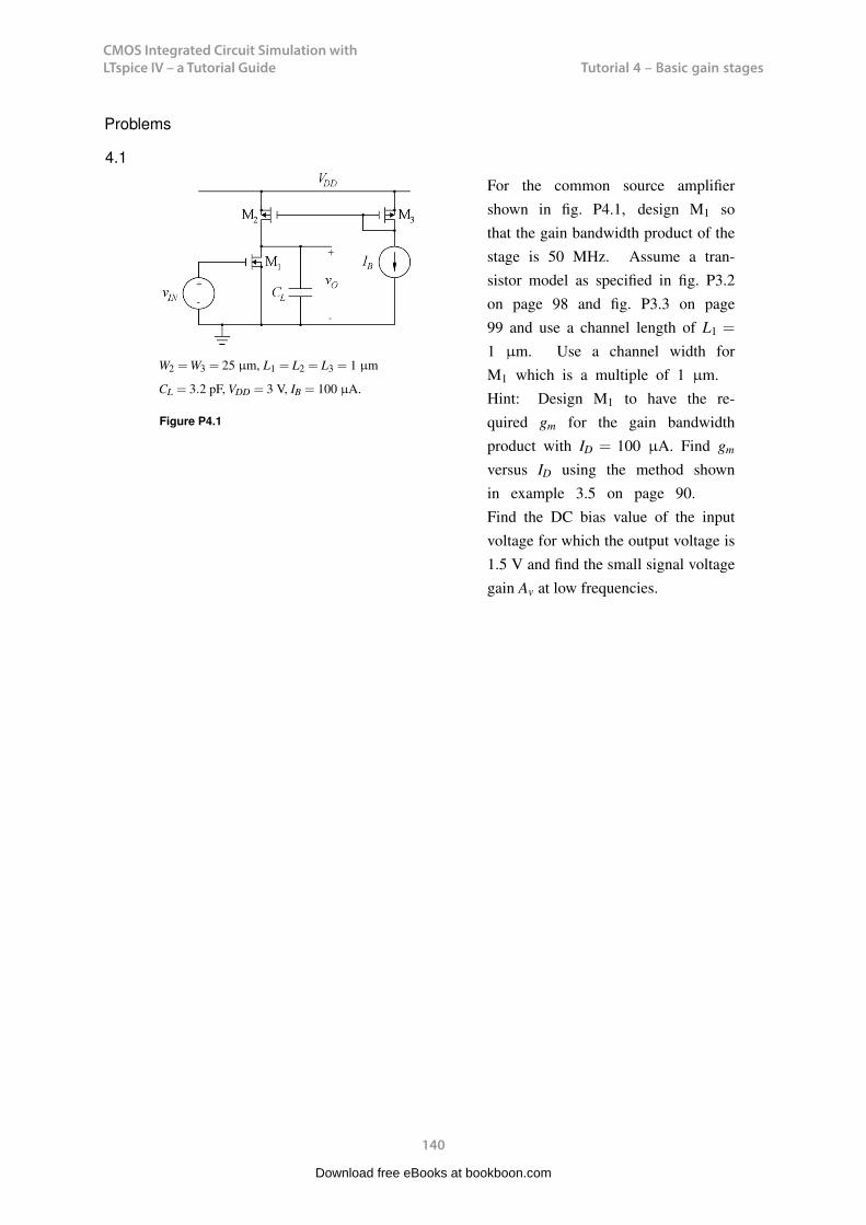
CMOS Integrated Circuit Simulation with LTspice IV – a Tutorial Guide
140
Tutorial 4 – Basic gain stagesCMOS Integrated Circuit Simulation with LTspice IV Tutorial 4
Problems
4.1
W2 =W3 = 25 µm, L1 = L2 = L3 = 1 µm
CL = 3.2 pF, VDD = 3 V, IB = 100 µA.
Figure P4.1
For the common source amplifiershown in fig. P4.1, design M1 sothat the gain bandwidth product of thestage is 50 MHz. Assume a tran-sistor model as specified in fig. P3.2on page 98 and fig. P3.3 on page99 and use a channel length of L1 =
1 µm. Use a channel width forM1 which is a multiple of 1 µm.Hint: Design M1 to have the re-quired gm for the gain bandwidthproduct with ID = 100 µA. Find gm
versus ID using the method shownin example 3.5 on page 90.Find the DC bias value of the inputvoltage for which the output voltage is1.5 V and find the small signal voltagegain Av at low frequencies.
140
Download free eBooks at bookboon.com
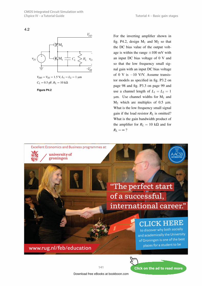
CMOS Integrated Circuit Simulation with LTspice IV – a Tutorial Guide
141
Tutorial 4 – Basic gain stagesCMOS Integrated Circuit Simulation with LTspice IV Tutorial 4
4.2
VDD =VSS = 1.5 V, L1 = L2 = 1 µm
CL = 0.5 pF, RL = 10 kΩ
Figure P4.2
For the inverting amplifier shown infig. P4.2, design M1 and M2 so thatthe DC bias value of the output volt-age is within the range ±100 mV withan input DC bias voltage of 0 V andso that the low frequency small sig-nal gain with an input DC bias voltageof 0 V is −10 V/V. Assume transis-tor models as specified in fig. P3.2 onpage 98 and fig. P3.3 on page 99 anduse a channel length of L1 = L2 = 1µm. Use channel widths for M1 andM2 which are multiples of 0.5 µm.What is the low frequency small signalgain if the load resistor RL is omitted?What is the gain bandwidth product ofthe amplifier for RL = 10 kΩ and forRL = ∞ ?
141
Download free eBooks at bookboon.com
Click on the ad to read moreClick on the ad to read moreClick on the ad to read moreClick on the ad to read moreClick on the ad to read moreClick on the ad to read moreClick on the ad to read moreClick on the ad to read moreClick on the ad to read moreClick on the ad to read moreClick on the ad to read moreClick on the ad to read moreClick on the ad to read moreClick on the ad to read moreClick on the ad to read moreClick on the ad to read moreClick on the ad to read moreClick on the ad to read moreClick on the ad to read moreClick on the ad to read moreClick on the ad to read moreClick on the ad to read moreClick on the ad to read moreClick on the ad to read moreClick on the ad to read moreClick on the ad to read moreClick on the ad to read moreClick on the ad to read moreClick on the ad to read moreClick on the ad to read moreClick on the ad to read moreClick on the ad to read moreClick on the ad to read moreClick on the ad to read moreClick on the ad to read moreClick on the ad to read moreClick on the ad to read moreClick on the ad to read moreClick on the ad to read moreClick on the ad to read moreClick on the ad to read moreClick on the ad to read moreClick on the ad to read moreClick on the ad to read moreClick on the ad to read moreClick on the ad to read moreClick on the ad to read moreClick on the ad to read moreClick on the ad to read more
“The perfect start of a successful, international career.”
CLICK HERE to discover why both socially
and academically the University
of Groningen is one of the best
places for a student to be www.rug.nl/feb/education
Excellent Economics and Business programmes at:
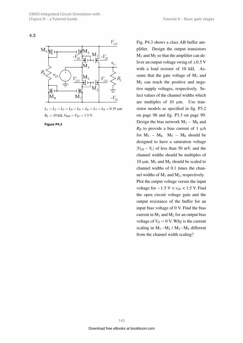
CMOS Integrated Circuit Simulation with LTspice IV – a Tutorial Guide
142
Tutorial 4 – Basic gain stagesCMOS Integrated Circuit Simulation with LTspice IV Tutorial 4
4.3
L1 = L2 = L3 = L4 = L5 = L6 = L7 = L8 = 0.35 µm
RL = 10 kΩ, VDD =VSS = 1.5 V.
Figure P4.3
Fig. P4.3 shows a class AB buffer am-plifier. Design the output transistorsM1 and M2 so that the amplifier can de-liver an output voltage swing of ±0.5 Vwith a load resistor of 10 kΩ. As-sume that the gate voltage of M1 andM2 can reach the positive and nega-tive supply voltages, respectively. Se-lect values of the channel widths whichare multiples of 10 µm. Use tran-sistor models as specified in fig. P3.2on page 98 and fig. P3.3 on page 99.Design the bias network M3 − M8 andRB to provide a bias current of 1 µAfor M3 − M8. M5 − M8 should bedesigned to have a saturation voltage|VGS −Vt | of less than 50 mV, and thechannel widths should be multiples of10 µm. M3 and M4 should be scaled tochannel widths of 0.1 times the chan-nel widths of M1 and M2, respectively.Plot the output voltage versus the inputvoltage for −1.5 V < vIN < 1.5 V. Findthe open circuit voltage gain and theoutput resistance of the buffer for aninput bias voltage of 0 V. Find the biascurrent in M1 and M2 for an output biasvoltage of VO = 0 V. Why is the currentscaling in M1−M2 / M3−M4 differentfrom the channel width scaling?
142
Download free eBooks at bookboon.com

CMOS Integrated Circuit Simulation with LTspice IV – a Tutorial Guide
143
Tutorial 4 – Basic gain stagesCMOS Integrated Circuit Simulation with LTspice IV Tutorial 4
4.4
L1 = L2 = 1 µm, W1 =W2 = 10 µmIB = 20 µA, VB = 1.5 V, VDD = 3 V.
.MODEL NMOS-SH nmos (Kp=190u Vto=0.57+Lambda=0.16 Gamma=0.50 Phi=0.7 TOX=8n+CGSO=0.2f CGBO=0.2f CGDO=0.2f CJ=1m)+CJSW=0.4n)
Figure P4.4
For the telescopic cascode shown infig. P4.4, find the bias value of VIN re-quired to give an output voltage of 2 V.Also find the small signal gain Avoc andoutput resistance ro at low frequencies.Find the small signal resistance rx toground from the node x between thesource of M2 and the drain of M1. As-sume a transistor model as shown infig. P4.4.
143
Download free eBooks at bookboon.com
Click on the ad to read moreClick on the ad to read moreClick on the ad to read moreClick on the ad to read moreClick on the ad to read moreClick on the ad to read moreClick on the ad to read moreClick on the ad to read moreClick on the ad to read moreClick on the ad to read moreClick on the ad to read moreClick on the ad to read moreClick on the ad to read moreClick on the ad to read moreClick on the ad to read moreClick on the ad to read moreClick on the ad to read moreClick on the ad to read moreClick on the ad to read moreClick on the ad to read moreClick on the ad to read moreClick on the ad to read moreClick on the ad to read moreClick on the ad to read moreClick on the ad to read moreClick on the ad to read moreClick on the ad to read moreClick on the ad to read moreClick on the ad to read moreClick on the ad to read moreClick on the ad to read moreClick on the ad to read moreClick on the ad to read moreClick on the ad to read moreClick on the ad to read moreClick on the ad to read moreClick on the ad to read moreClick on the ad to read moreClick on the ad to read moreClick on the ad to read moreClick on the ad to read moreClick on the ad to read moreClick on the ad to read moreClick on the ad to read moreClick on the ad to read moreClick on the ad to read moreClick on the ad to read moreClick on the ad to read moreClick on the ad to read moreClick on the ad to read more
89,000 kmIn the past four years we have drilled
That’s more than twice around the world.
careers.slb.com
What will you be?
1 Based on Fortune 500 ranking 2011. Copyright © 2015 Schlumberger. All rights reserved.
Who are we?We are the world’s largest oilfield services company1. Working globally—often in remote and challenging locations— we invent, design, engineer, and apply technology to help our customers find and produce oil and gas safely.
Who are we looking for?Every year, we need thousands of graduates to begin dynamic careers in the following domains:n Engineering, Research and Operationsn Geoscience and Petrotechnicaln Commercial and Business
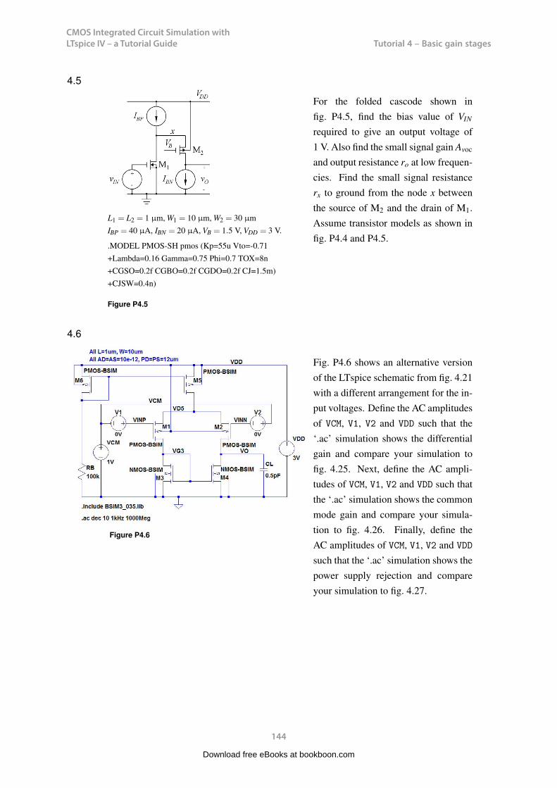
CMOS Integrated Circuit Simulation with LTspice IV – a Tutorial Guide
144
Tutorial 4 – Basic gain stagesCMOS Integrated Circuit Simulation with LTspice IV Tutorial 4
4.5
L1 = L2 = 1 µm, W1 = 10 µm, W2 = 30 µmIBP = 40 µA, IBN = 20 µA, VB = 1.5 V, VDD = 3 V.
.MODEL PMOS-SH pmos (Kp=55u Vto=-0.71+Lambda=0.16 Gamma=0.75 Phi=0.7 TOX=8n+CGSO=0.2f CGBO=0.2f CGDO=0.2f CJ=1.5m)+CJSW=0.4n)
Figure P4.5
For the folded cascode shown infig. P4.5, find the bias value of VIN
required to give an output voltage of1 V. Also find the small signal gain Avoc
and output resistance ro at low frequen-cies. Find the small signal resistancerx to ground from the node x betweenthe source of M2 and the drain of M1.Assume transistor models as shown infig. P4.4 and P4.5.
4.6
Figure P4.6
Fig. P4.6 shows an alternative versionof the LTspice schematic from fig. 4.21with a different arrangement for the in-put voltages. Define the AC amplitudesof VCM, V1, V2 and VDD such that the‘.ac’ simulation shows the differentialgain and compare your simulation tofig. 4.25. Next, define the AC ampli-tudes of VCM, V1, V2 and VDD such thatthe ‘.ac’ simulation shows the commonmode gain and compare your simula-tion to fig. 4.26. Finally, define theAC amplitudes of VCM, V1, V2 and VDD
such that the ‘.ac’ simulation shows thepower supply rejection and compareyour simulation to fig. 4.27.
144
Download free eBooks at bookboon.com
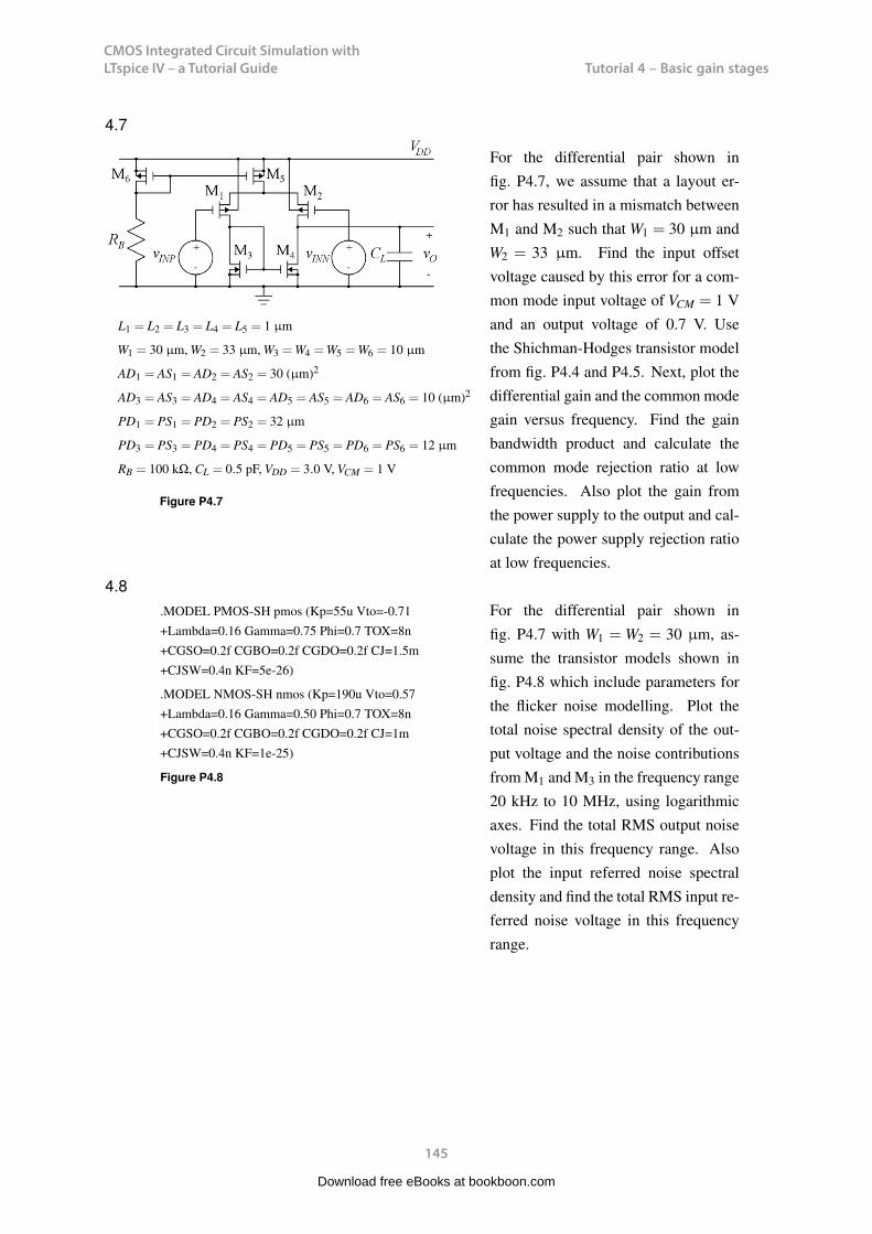
CMOS Integrated Circuit Simulation with LTspice IV – a Tutorial Guide
145
Tutorial 4 – Basic gain stagesCMOS Integrated Circuit Simulation with LTspice IV Tutorial 4
4.7
L1 = L2 = L3 = L4 = L5 = 1 µm
W1 = 30 µm, W2 = 33 µm, W3 =W4 =W5 =W6 = 10 µm
AD1 = AS1 = AD2 = AS2 = 30 (µm)2
AD3 = AS3 = AD4 = AS4 = AD5 = AS5 = AD6 = AS6 = 10 (µm)2
PD1 = PS1 = PD2 = PS2 = 32 µm
PD3 = PS3 = PD4 = PS4 = PD5 = PS5 = PD6 = PS6 = 12 µm
RB = 100 kΩ, CL = 0.5 pF, VDD = 3.0 V, VCM = 1 V
Figure P4.7
For the differential pair shown infig. P4.7, we assume that a layout er-ror has resulted in a mismatch betweenM1 and M2 such that W1 = 30 µm andW2 = 33 µm. Find the input offsetvoltage caused by this error for a com-mon mode input voltage of VCM = 1 Vand an output voltage of 0.7 V. Usethe Shichman-Hodges transistor modelfrom fig. P4.4 and P4.5. Next, plot thedifferential gain and the common modegain versus frequency. Find the gainbandwidth product and calculate thecommon mode rejection ratio at lowfrequencies. Also plot the gain fromthe power supply to the output and cal-culate the power supply rejection ratioat low frequencies.
4.8.MODEL PMOS-SH pmos (Kp=55u Vto=-0.71+Lambda=0.16 Gamma=0.75 Phi=0.7 TOX=8n+CGSO=0.2f CGBO=0.2f CGDO=0.2f CJ=1.5m+CJSW=0.4n KF=5e-26)
.MODEL NMOS-SH nmos (Kp=190u Vto=0.57+Lambda=0.16 Gamma=0.50 Phi=0.7 TOX=8n+CGSO=0.2f CGBO=0.2f CGDO=0.2f CJ=1m+CJSW=0.4n KF=1e-25)
Figure P4.8
For the differential pair shown infig. P4.7 with W1 = W2 = 30 µm, as-sume the transistor models shown infig. P4.8 which include parameters forthe flicker noise modelling. Plot thetotal noise spectral density of the out-put voltage and the noise contributionsfrom M1 and M3 in the frequency range20 kHz to 10 MHz, using logarithmicaxes. Find the total RMS output noisevoltage in this frequency range. Alsoplot the input referred noise spectraldensity and find the total RMS input re-ferred noise voltage in this frequencyrange.
145
Download free eBooks at bookboon.com

CMOS Integrated Circuit Simulation with LTspice IV – a Tutorial Guide
146
Tutorial 4 – Basic gain stagesCMOS Integrated Circuit Simulation with LTspice IV Tutorial 4
Answers
4.1: W1 = 28 µm; VIN = 0.7735 V; Av = 38 dB.
4.2: W1 = 6.5 µm; W2 = 21 µm; Avoc =−43 V/V; GBW(RL=10 kΩ) = GBW(RL=∞) = 405 MHz.
4.3: W1 = 30 µm; W2 = 370 µm; W3 = 3 µm; W4 = 37 µm; W5 = W6 = 30 µm; W7 = W8 = 10 µm;RB = 1.84 MΩ; Avoc = 0.95 V/V; ro = 1019 Ω; ID1 = ID2 = 18.3 µA;|VDS| larger for M1−M2 than for M3−M4 and |Vth| smaller for M1−M2 than for M3−M4.
4.4: VIN = 708.21 mV; Avoc = 83 dB, ro = 49 MΩ, rm = 344 kΩ.
4.5: VIN = 692.40 mV; Avoc = 87 dB, ro = 66 MΩ, rm = 439 kΩ.
4.6: Differential gain: VCM = 0, V1 = 0.5, V2 = 0.5 and VDD = 0;Common mode gain: VCM = 1, V1 = 0, V2 = 0 and VDD = 0;Power supply rejection: VCM = 0, V1 = 0, V2 = 0 and VDD = 1.
4.7: Voff =−4.2 mV; GBW = 60 MHz; CMRR = 66 dB; PSRR = 57 dB.
4.8: Von, RMS = 1.3 mV; Vin, RMS = 48 µV.
146
Download free eBooks at bookboon.com
Click on the ad to read moreClick on the ad to read moreClick on the ad to read moreClick on the ad to read moreClick on the ad to read moreClick on the ad to read moreClick on the ad to read moreClick on the ad to read moreClick on the ad to read moreClick on the ad to read moreClick on the ad to read moreClick on the ad to read moreClick on the ad to read moreClick on the ad to read moreClick on the ad to read moreClick on the ad to read moreClick on the ad to read moreClick on the ad to read moreClick on the ad to read moreClick on the ad to read moreClick on the ad to read moreClick on the ad to read moreClick on the ad to read moreClick on the ad to read moreClick on the ad to read moreClick on the ad to read moreClick on the ad to read moreClick on the ad to read moreClick on the ad to read moreClick on the ad to read moreClick on the ad to read moreClick on the ad to read moreClick on the ad to read moreClick on the ad to read moreClick on the ad to read moreClick on the ad to read moreClick on the ad to read moreClick on the ad to read moreClick on the ad to read moreClick on the ad to read moreClick on the ad to read moreClick on the ad to read moreClick on the ad to read moreClick on the ad to read moreClick on the ad to read moreClick on the ad to read moreClick on the ad to read moreClick on the ad to read moreClick on the ad to read moreClick on the ad to read moreClick on the ad to read more
American online LIGS University
enroll by September 30th, 2014 and
save up to 16% on the tuition!
pay in 10 installments / 2 years
Interactive Online education visit www.ligsuniversity.com to
find out more!
is currently enrolling in theInteractive Online BBA, MBA, MSc,
DBA and PhD programs:
Note: LIGS University is not accredited by any nationally recognized accrediting agency listed by the US Secretary of Education. More info here.
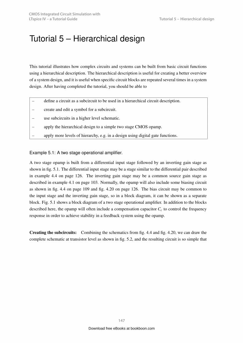
CMOS Integrated Circuit Simulation with LTspice IV – a Tutorial Guide
147
Tutorial 5 – Hierarchical design
CMOS Integrated Circuit Simulation with LTspice IV Tutorial 5
Tutorial 5 – Hierarchical design
This tutorial illustrates how complex circuits and systems can be built from basic circuit functionsusing a hierarchical description. The hierarchical description is useful for creating a better overviewof a system design, and it is useful when specific circuit blocks are repeated several times in a systemdesign. After having completed the tutorial, you should be able to
– define a circuit as a subcircuit to be used in a hierarchical circuit description.
– create and edit a symbol for a subcircuit.
– use subcircuits in a higher level schematic.
– apply the hierarchical design to a simple two stage CMOS opamp.
– apply more levels of hierarchy, e.g. in a design using digital gate functions.
Example 5.1: A two stage operational amplifier.
A two stage opamp is built from a differential input stage followed by an inverting gain stage asshown in fig. 5.1. The differential input stage may be a stage similar to the differential pair describedin example 4.4 on page 126. The inverting gain stage may be a common source gain stage asdescribed in example 4.1 on page 103. Normally, the opamp will also include some biasing circuitas shown in fig. 4.4 on page 109 and fig. 4.20 on page 126. The bias circuit may be common tothe input stage and the inverting gain stage, so in a block diagram, it can be shown as a separateblock. Fig. 5.1 shows a block diagram of a two stage operational amplifier. In addition to the blocksdescribed here, the opamp will often include a compensation capacitor Cc to control the frequencyresponse in order to achieve stability in a feedback system using the opamp.
Creating the subcircuits: Combining the schematics from fig. 4.4 and fig. 4.20, we can draw thecomplete schematic at transistor level as shown in fig. 5.2, and the resulting circuit is so simple that
147
Download free eBooks at bookboon.com
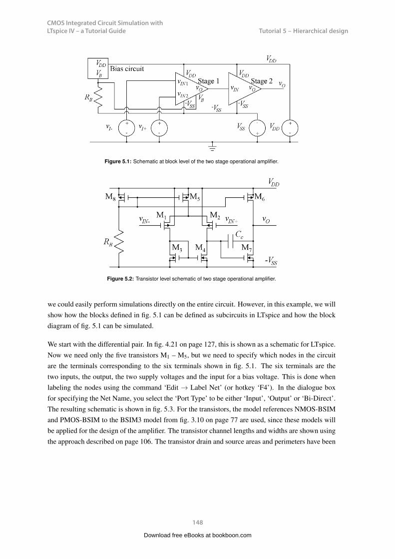
CMOS Integrated Circuit Simulation with LTspice IV – a Tutorial Guide
148
Tutorial 5 – Hierarchical designCMOS Integrated Circuit Simulation with LTspice IV Tutorial 5
Figure 5.1: Schematic at block level of the two stage operational amplifier.
Figure 5.2: Transistor level schematic of two stage operational amplifier.
we could easily perform simulations directly on the entire circuit. However, in this example, we willshow how the blocks defined in fig. 5.1 can be defined as subcircuits in LTspice and how the blockdiagram of fig. 5.1 can be simulated.
We start with the differential pair. In fig. 4.21 on page 127, this is shown as a schematic for LTspice.Now we need only the five transistors M1 – M5, but we need to specify which nodes in the circuitare the terminals corresponding to the six terminals shown in fig. 5.1. The six terminals are thetwo inputs, the output, the two supply voltages and the input for a bias voltage. This is done whenlabeling the nodes using the command ‘Edit → Label Net’ (or hotkey ‘F4’). In the dialogue boxfor specifying the Net Name, you select the ‘Port Type’ to be either ‘Input’, ‘Output’ or ‘Bi-Direct’.The resulting schematic is shown in fig. 5.3. For the transistors, the model references NMOS-BSIMand PMOS-BSIM to the BSIM3 model from fig. 3.10 on page 77 are used, since these models willbe applied for the design of the amplifier. The transistor channel lengths and widths are shown usingthe approach described on page 106. The transistor drain and source areas and perimeters have been
148
Download free eBooks at bookboon.com

CMOS Integrated Circuit Simulation with LTspice IV – a Tutorial Guide
149
Tutorial 5 – Hierarchical designCMOS Integrated Circuit Simulation with LTspice IV Tutorial 5
Figure 5.3: LTspice schematic for differential pair subcircuit.
specified using source and drain areas of 3 times W times the minimum length and perimeters ofW plus 6 times the minimum length, i.e. slightly larger than the minimum sizes indicated on page75. The dimensions have (arbitrarily) been chosen to the same as in fig. 4.21.
Now the subcircuit schematic is complete, and we need a symbol for it, so that it can be used at ablock level as in fig. 5.1. This is achieved by the command ‘Hierarchy → Open this Sheet’s Symbol’.A new window opens with a message from LTspice: ‘Couldn’t find this sheet’s symbol. Shall I try to
149
Download free eBooks at bookboon.com
Click on the ad to read moreClick on the ad to read moreClick on the ad to read moreClick on the ad to read moreClick on the ad to read moreClick on the ad to read moreClick on the ad to read moreClick on the ad to read moreClick on the ad to read moreClick on the ad to read moreClick on the ad to read moreClick on the ad to read moreClick on the ad to read moreClick on the ad to read moreClick on the ad to read moreClick on the ad to read moreClick on the ad to read moreClick on the ad to read moreClick on the ad to read moreClick on the ad to read moreClick on the ad to read moreClick on the ad to read moreClick on the ad to read moreClick on the ad to read moreClick on the ad to read moreClick on the ad to read moreClick on the ad to read moreClick on the ad to read moreClick on the ad to read moreClick on the ad to read moreClick on the ad to read moreClick on the ad to read moreClick on the ad to read moreClick on the ad to read moreClick on the ad to read moreClick on the ad to read moreClick on the ad to read moreClick on the ad to read moreClick on the ad to read moreClick on the ad to read moreClick on the ad to read moreClick on the ad to read moreClick on the ad to read moreClick on the ad to read moreClick on the ad to read moreClick on the ad to read moreClick on the ad to read moreClick on the ad to read moreClick on the ad to read moreClick on the ad to read moreClick on the ad to read moreClick on the ad to read more
.
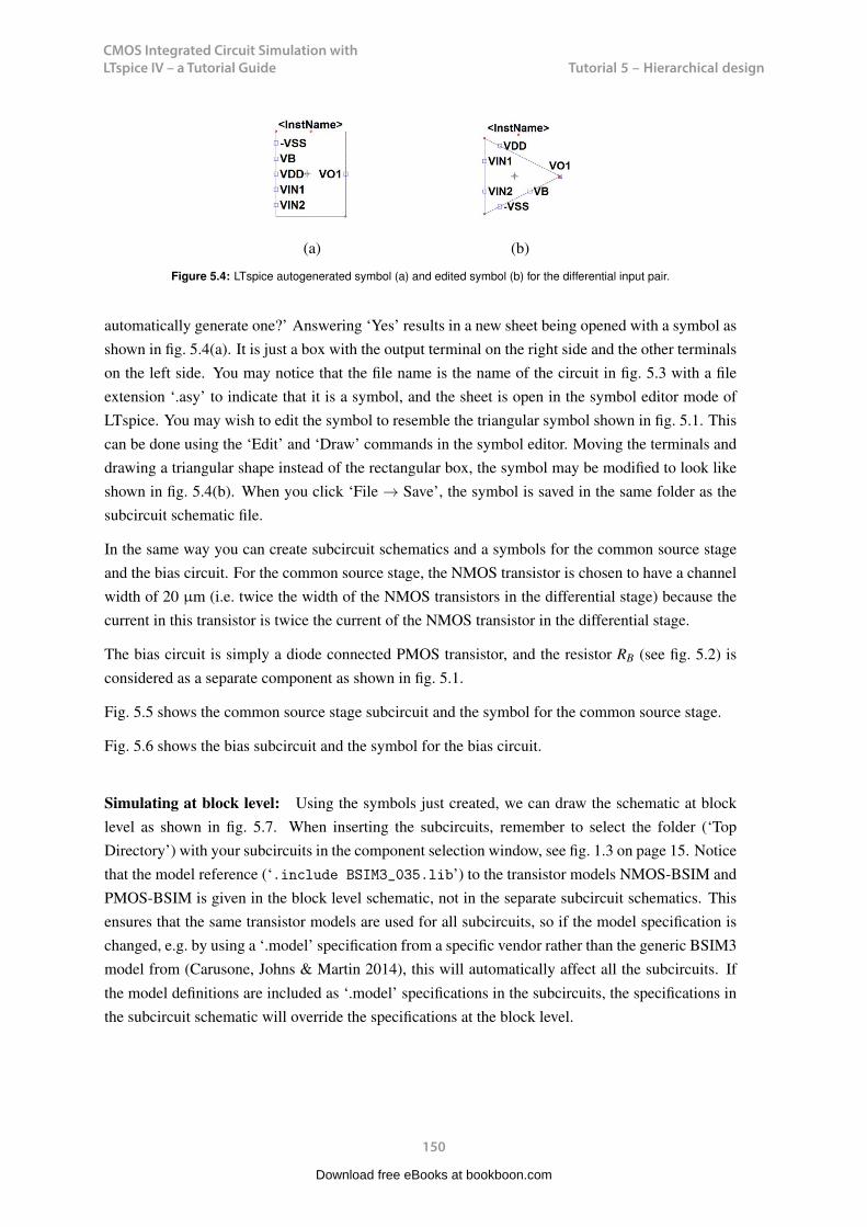
CMOS Integrated Circuit Simulation with LTspice IV – a Tutorial Guide
150
Tutorial 5 – Hierarchical designCMOS Integrated Circuit Simulation with LTspice IV Tutorial 5
(a) (b)
Figure 5.4: LTspice autogenerated symbol (a) and edited symbol (b) for the differential input pair.
automatically generate one?’ Answering ‘Yes’ results in a new sheet being opened with a symbol asshown in fig. 5.4(a). It is just a box with the output terminal on the right side and the other terminalson the left side. You may notice that the file name is the name of the circuit in fig. 5.3 with a fileextension ‘.asy’ to indicate that it is a symbol, and the sheet is open in the symbol editor mode ofLTspice. You may wish to edit the symbol to resemble the triangular symbol shown in fig. 5.1. Thiscan be done using the ‘Edit’ and ‘Draw’ commands in the symbol editor. Moving the terminals anddrawing a triangular shape instead of the rectangular box, the symbol may be modified to look likeshown in fig. 5.4(b). When you click ‘File → Save’, the symbol is saved in the same folder as thesubcircuit schematic file.
In the same way you can create subcircuit schematics and a symbols for the common source stageand the bias circuit. For the common source stage, the NMOS transistor is chosen to have a channelwidth of 20 µm (i.e. twice the width of the NMOS transistors in the differential stage) because thecurrent in this transistor is twice the current of the NMOS transistor in the differential stage.
The bias circuit is simply a diode connected PMOS transistor, and the resistor RB (see fig. 5.2) isconsidered as a separate component as shown in fig. 5.1.
Fig. 5.5 shows the common source stage subcircuit and the symbol for the common source stage.
Fig. 5.6 shows the bias subcircuit and the symbol for the bias circuit.
Simulating at block level: Using the symbols just created, we can draw the schematic at blocklevel as shown in fig. 5.7. When inserting the subcircuits, remember to select the folder (‘TopDirectory’) with your subcircuits in the component selection window, see fig. 1.3 on page 15. Noticethat the model reference (‘.include BSIM3_035.lib’) to the transistor models NMOS-BSIM andPMOS-BSIM is given in the block level schematic, not in the separate subcircuit schematics. Thisensures that the same transistor models are used for all subcircuits, so if the model specification ischanged, e.g. by using a ‘.model’ specification from a specific vendor rather than the generic BSIM3model from (Carusone, Johns & Martin 2014), this will automatically affect all the subcircuits. If
150
CMOS Integrated Circuit Simulation with LTspice IV Tutorial 5
(a) (b)
Figure 5.5: LTspice schematic (a) and symbol (b) for the common source stage.
(a) (b)
Figure 5.6: LTspice schematic (a) and symbol (b) for the bias circuit.
the model definitions are included as ‘.model’ specifications in the subcircuits, the specifications inthe subcircuit schematic will override the specifications at the block level.
151
Download free eBooks at bookboon.com

CMOS Integrated Circuit Simulation with LTspice IV – a Tutorial Guide
151
Tutorial 5 – Hierarchical designCMOS Integrated Circuit Simulation with LTspice IV Tutorial 5
(a) (b)
Figure 5.5: LTspice schematic (a) and symbol (b) for the common source stage.
(a) (b)
Figure 5.6: LTspice schematic (a) and symbol (b) for the bias circuit.
the model definitions are included as ‘.model’ specifications in the subcircuits, the specifications inthe subcircuit schematic will override the specifications at the block level.
151
Download free eBooks at bookboon.com
Click on the ad to read moreClick on the ad to read moreClick on the ad to read moreClick on the ad to read moreClick on the ad to read moreClick on the ad to read moreClick on the ad to read moreClick on the ad to read moreClick on the ad to read moreClick on the ad to read moreClick on the ad to read moreClick on the ad to read moreClick on the ad to read moreClick on the ad to read moreClick on the ad to read moreClick on the ad to read moreClick on the ad to read moreClick on the ad to read moreClick on the ad to read moreClick on the ad to read moreClick on the ad to read moreClick on the ad to read moreClick on the ad to read moreClick on the ad to read moreClick on the ad to read moreClick on the ad to read moreClick on the ad to read moreClick on the ad to read moreClick on the ad to read moreClick on the ad to read moreClick on the ad to read moreClick on the ad to read moreClick on the ad to read moreClick on the ad to read moreClick on the ad to read moreClick on the ad to read moreClick on the ad to read moreClick on the ad to read moreClick on the ad to read moreClick on the ad to read moreClick on the ad to read moreClick on the ad to read moreClick on the ad to read moreClick on the ad to read moreClick on the ad to read moreClick on the ad to read moreClick on the ad to read moreClick on the ad to read moreClick on the ad to read moreClick on the ad to read moreClick on the ad to read moreClick on the ad to read moreClick on the ad to read more
www.mastersopenday.nl
Visit us and find out why we are the best!Master’s Open Day: 22 February 2014
Join the best atthe Maastricht UniversitySchool of Business andEconomics!
Top master’s programmes• 33rdplaceFinancialTimesworldwideranking:MScInternationalBusiness
• 1stplace:MScInternationalBusiness• 1stplace:MScFinancialEconomics• 2ndplace:MScManagementofLearning• 2ndplace:MScEconomics• 2ndplace:MScEconometricsandOperationsResearch• 2ndplace:MScGlobalSupplyChainManagementandChange
Sources: Keuzegids Master ranking 2013; Elsevier ‘Beste Studies’ ranking 2012; Financial Times Global Masters in Management ranking 2012
MaastrichtUniversity is
the best specialistuniversity in the
Netherlands(Elsevier)
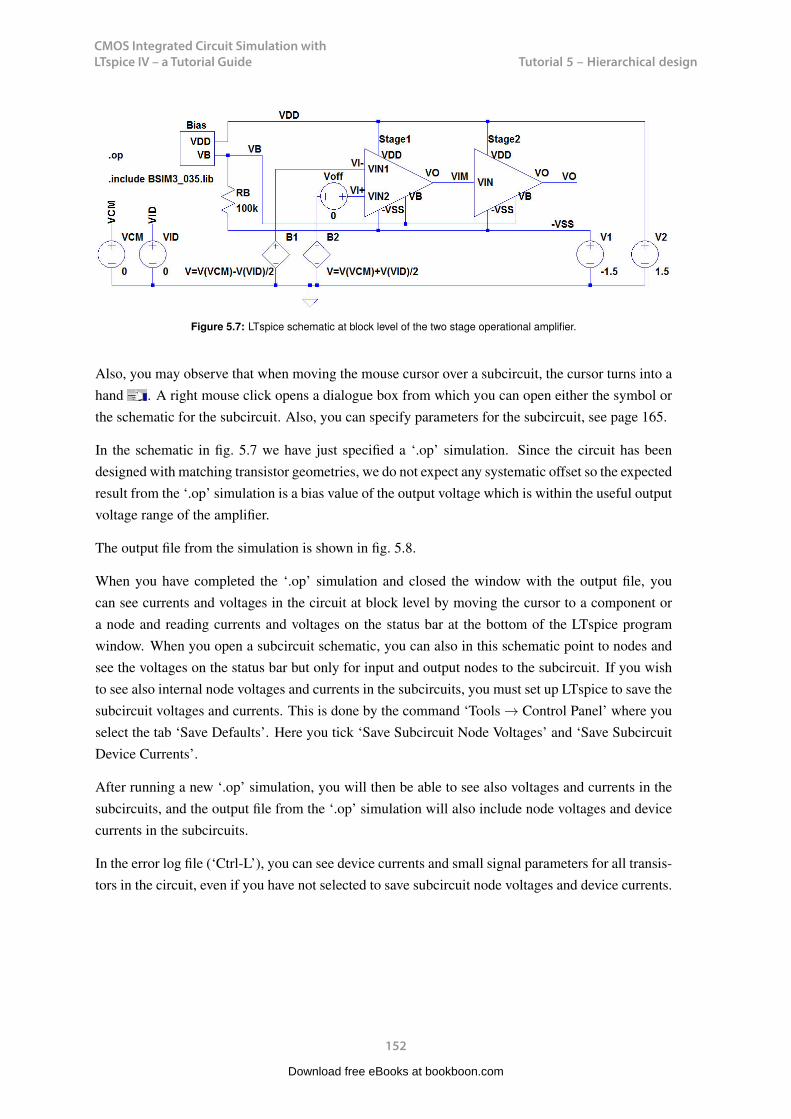
CMOS Integrated Circuit Simulation with LTspice IV – a Tutorial Guide
152
Tutorial 5 – Hierarchical designCMOS Integrated Circuit Simulation with LTspice IV Tutorial 5
Figure 5.7: LTspice schematic at block level of the two stage operational amplifier.
Also, you may observe that when moving the mouse cursor over a subcircuit, the cursor turns into ahand . A right mouse click opens a dialogue box from which you can open either the symbol orthe schematic for the subcircuit. Also, you can specify parameters for the subcircuit, see page 165.
In the schematic in fig. 5.7 we have just specified a ‘.op’ simulation. Since the circuit has beendesigned with matching transistor geometries, we do not expect any systematic offset so the expectedresult from the ‘.op’ simulation is a bias value of the output voltage which is within the useful outputvoltage range of the amplifier.
The output file from the simulation is shown in fig. 5.8.
When you have completed the ‘.op’ simulation and closed the window with the output file, youcan see currents and voltages in the circuit at block level by moving the cursor to a component ora node and reading currents and voltages on the status bar at the bottom of the LTspice programwindow. When you open a subcircuit schematic, you can also in this schematic point to nodes andsee the voltages on the status bar but only for input and output nodes to the subcircuit. If you wishto see also internal node voltages and currents in the subcircuits, you must set up LTspice to save thesubcircuit voltages and currents. This is done by the command ‘Tools → Control Panel’ where youselect the tab ‘Save Defaults’. Here you tick ‘Save Subcircuit Node Voltages’ and ‘Save SubcircuitDevice Currents’.
After running a new ‘.op’ simulation, you will then be able to see also voltages and currents in thesubcircuits, and the output file from the ‘.op’ simulation will also include node voltages and devicecurrents in the subcircuits.
In the error log file (‘Ctrl-L’), you can see device currents and small signal parameters for all transis-tors in the circuit, even if you have not selected to save subcircuit node voltages and device currents.
152
Download free eBooks at bookboon.com

CMOS Integrated Circuit Simulation with LTspice IV – a Tutorial Guide
153
Tutorial 5 – Hierarchical designCMOS Integrated Circuit Simulation with LTspice IV Tutorial 5
Output file:
- - - Operating point - - -
V(vim): -0.81608 voltageV(vi+): 0 voltageV(vdd): 1.5 voltageV(vi-): 0 voltageV(vb): 0.55281 voltageV(-vss): -1.5 voltageV(vid): 0 voltageV(vcm): 0 voltageV(n001): 0 voltageV(vo): -0.479621 voltageI(B1): 0 device_currentI(B2): 0 device_currentI(RB): 2.05281e-005 device_currentI(V2): -6.2341e-005 device_currentI(V1): 6.2341e-005 device_currentI(Voff): 0 device_currentI(Vcm): 0 device_currentI(Vid): 0 device_currentIx(stage1:-VSS): -1.9599e-005 subckt_currentIx(stage1:VB): 0 subckt_currentIx(stage1:VDD): 1.9599e-005 subckt_currentIx(stage1:VIN1): 0 subckt_currentIx(stage1:VIN2): 0 subckt_currentIx(stage1:VO): -3.89635e-020 subckt_currentIx(bias:VB): -2.05281e-005 subckt_currentIx(bias:VDD): 2.05281e-005 subckt_currentIx(stage2:-VSS): -2.22139e-005 subckt_currentIx(stage2:VB): 0 subckt_currentIx(stage2:VDD): 2.22139e-005 subckt_currentIx(stage2:VIN): 0 subckt_currentIx(stage2:VO): -6.77626e-020 subckt_current
Figure 5.8: Output file from the ‘.op’ simulation of the circuit in fig 5.7.
153
Download free eBooks at bookboon.com
Click on the ad to read moreClick on the ad to read moreClick on the ad to read moreClick on the ad to read moreClick on the ad to read moreClick on the ad to read moreClick on the ad to read moreClick on the ad to read moreClick on the ad to read moreClick on the ad to read moreClick on the ad to read moreClick on the ad to read moreClick on the ad to read moreClick on the ad to read moreClick on the ad to read moreClick on the ad to read moreClick on the ad to read moreClick on the ad to read moreClick on the ad to read moreClick on the ad to read moreClick on the ad to read moreClick on the ad to read moreClick on the ad to read moreClick on the ad to read moreClick on the ad to read moreClick on the ad to read moreClick on the ad to read moreClick on the ad to read moreClick on the ad to read moreClick on the ad to read moreClick on the ad to read moreClick on the ad to read moreClick on the ad to read moreClick on the ad to read moreClick on the ad to read moreClick on the ad to read moreClick on the ad to read moreClick on the ad to read moreClick on the ad to read moreClick on the ad to read moreClick on the ad to read moreClick on the ad to read moreClick on the ad to read moreClick on the ad to read moreClick on the ad to read moreClick on the ad to read moreClick on the ad to read moreClick on the ad to read moreClick on the ad to read moreClick on the ad to read moreClick on the ad to read moreClick on the ad to read moreClick on the ad to read moreClick on the ad to read more
- ©
Pho
tono
nsto
p
> Apply now
redefine your future
AxA globAl grAduAte progrAm 2015
axa_ad_grad_prog_170x115.indd 1 19/12/13 16:36
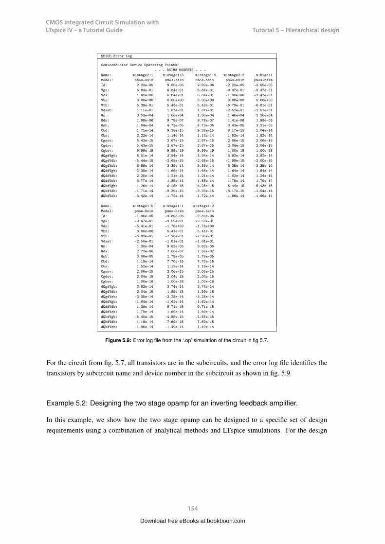
CMOS Integrated Circuit Simulation with LTspice IV – a Tutorial Guide
154
Tutorial 5 – Hierarchical designCMOS Integrated Circuit Simulation with LTspice IV Tutorial 5
SPICE Error Log
Semiconductor Device Operating Points:- - - BSIM3 MOSFETS - - -
Name: m:stage2:1 m:stage1:3 m:stage1:4 m:stage2:2 m:bias:1Model: nmos-bsim nmos-bsim nmos-bsim pmos-bsim pmos-bsimId: 2.22e-05 9.80e-06 9.80e-06 -2.22e-05 -2.05e-05Vgs: 6.84e-01 6.84e-01 6.84e-01 -9.47e-01 -9.47e-01Vds: 1.02e+00 6.84e-01 6.84e-01 -1.98e+00 -9.47e-01Vbs: 0.00e+00 0.00e+00 0.00e+00 0.00e+00 0.00e+00Vth: 5.39e-01 5.43e-01 5.43e-01 -6.79e-01 -6.81e-01Vdsat: 1.11e-01 1.07e-01 1.07e-01 -2.52e-01 -2.51e-01Gm: 3.52e-04 1.60e-04 1.60e-04 1.46e-04 1.36e-04Gds: 1.98e-06 9.78e-07 9.78e-07 1.41e-06 1.98e-06Gmb: 1.04e-04 4.73e-05 4.73e-05 3.43e-05 3.21e-05Cbd: 1.71e-14 9.38e-15 9.38e-15 8.17e-15 1.04e-14Cbs: 2.22e-14 1.14e-14 1.14e-14 1.52e-14 1.52e-14Cgsov: 5.43e-15 2.67e-15 2.67e-15 2.06e-15 2.06e-15Cgdov: 5.43e-15 2.67e-15 2.67e-15 2.04e-15 2.04e-15Cgbov: 9.99e-19 9.99e-19 9.99e-19 1.00e-18 1.00e-18dQgdVgb: 8.01e-14 3.94e-14 3.94e-14 3.82e-14 3.82e-14dQgdVdb: -5.44e-15 -2.68e-15 -2.68e-15 -1.99e-15 -2.00e-15dQgdVsb: -6.89e-14 -3.39e-14 -3.39e-14 -3.35e-14 -3.35e-14dQddVgb: -3.38e-14 -1.66e-14 -1.66e-14 -1.64e-14 -1.64e-14dQddVdb: 2.25e-14 1.21e-14 1.21e-14 1.02e-14 1.24e-14dQddVsb: 3.77e-14 1.85e-14 1.85e-14 1.79e-14 1.79e-14dQbdVgb: -1.26e-14 -6.25e-15 -6.25e-15 -5.44e-15 -5.43e-15dQbdVdb: -1.71e-14 -9.39e-15 -9.39e-15 -8.17e-15 -1.04e-14dQbdVsb: -3.42e-14 -1.72e-14 -1.72e-14 -1.96e-14 -1.96e-14
Name: m:stage1:5 m:stage1:1 m:stage1:2Model: pmos-bsim pmos-bsim pmos-bsimId: -1.96e-05 -9.80e-06 -9.80e-06Vgs: -9.47e-01 -9.59e-01 -9.59e-01Vds: -5.41e-01 -1.78e+00 -1.78e+00Vbs: 0.00e+00 5.41e-01 5.41e-01Vth: -6.82e-01 -7.96e-01 -7.96e-01Vdsat: -2.50e-01 -1.81e-01 -1.81e-01Gm: 1.30e-04 9.62e-05 9.62e-05Gds: 2.72e-06 7.66e-07 7.66e-07Gmb: 3.06e-05 1.78e-05 1.78e-05Cbd: 1.19e-14 7.70e-15 7.70e-15Cbs: 1.52e-14 1.19e-14 1.19e-14Cgsov: 2.06e-15 2.06e-15 2.06e-15Cgdov: 2.04e-15 2.04e-15 2.04e-15Cgbov: 1.00e-18 1.00e-18 1.00e-18dQgdVgb: 3.82e-14 3.74e-14 3.74e-14dQgdVdb: -2.04e-15 -1.99e-15 -1.99e-15dQgdVsb: -3.35e-14 -3.28e-14 -3.28e-14dQddVgb: -1.64e-14 -1.62e-14 -1.62e-14dQddVdb: 1.39e-14 9.71e-15 9.71e-15dQddVsb: 1.79e-14 1.69e-14 1.69e-14dQbdVgb: -5.40e-15 -4.85e-15 -4.85e-15dQbdVdb: -1.19e-14 -7.69e-15 -7.69e-15dQbdVsb: -1.96e-14 -1.49e-14 -1.49e-14
Figure 5.9: Error log file from the ‘.op’ simulation of the circuit in fig 5.7.
For the circuit from fig. 5.7, all transistors are in the subcircuits, and the error log file identifies thetransistors by subcircuit name and device number in the subcircuit as shown in fig. 5.9.
Example 5.2: Designing the two stage opamp for an inverting feedback amplifier.
In this example, we show how the two stage opamp can be designed to a specific set of designrequirements using a combination of analytical methods and LTspice simulations. For the design
154
Download free eBooks at bookboon.com
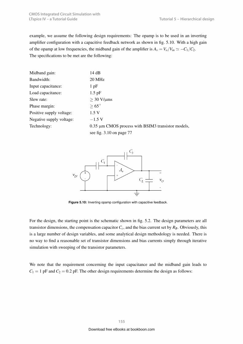
CMOS Integrated Circuit Simulation with LTspice IV – a Tutorial Guide
155
Tutorial 5 – Hierarchical designCMOS Integrated Circuit Simulation with LTspice IV Tutorial 5
example, we assume the following design requirements: The opamp is to be used in an invertingamplifier configuration with a capacitive feedback network as shown in fig. 5.10. With a high gainof the opamp at low frequencies, the midband gain of the amplifier is Av =Vo/Vin −C1/C2.The specifications to be met are the following:
Midband gain: 14 dBBandwidth: 20 MHzInput capacitance: 1 pFLoad capacitance: 1.5 pFSlew rate: ≥ 30 V/µmsPhase margin: ≥ 65
Positive supply voltage: 1.5 VNegative supply voltage: −1.5 VTechnology: 0.35 µm CMOS process with BSIM3 transistor models,
see fig. 3.10 on page 77
Figure 5.10: Inverting opamp configuration with capacitive feedback.
For the design, the starting point is the schematic shown in fig. 5.2. The design parameters are alltransistor dimensions, the compensation capacitor Cc, and the bias current set by RB. Obviously, thisis a large number of design variables, and some analytical design methodology is needed. There isno way to find a reasonable set of transistor dimensions and bias currents simply through iterativesimulation with sweeping of the transistor parameters.
We note that the requirement concerning the input capacitance and the midband gain leads toC1 = 1 pF and C2 = 0.2 pF. The other design requirements determine the design as follows:
155
Download free eBooks at bookboon.com

CMOS Integrated Circuit Simulation with LTspice IV – a Tutorial Guide
156
Tutorial 5 – Hierarchical designCMOS Integrated Circuit Simulation with LTspice IV Tutorial 5
– The bandwidth specification, BW, puts a constraint on the transconductance of the differ-ential input transistors and the compensation capacitor Cc which determine the unity gainbandwidth of the opamp.
– The specification for the phase margin, PM, puts constraints on the location of non-dominant poles and zeros in the opamp.
– The slew rate specification, SR, puts constraints on the bias current for M5 and M6 infig. 5.2. The bias currents must be large enough to slew the voltages on the load capaci-tance, the feedback capacitors and the compensation capacitor.
For the analytical approach, we base the design on the analysis of the two stage opamp presentedin (Carusone, Johns & Martin 2012, chapter 6). Examining the feedback configuration, we findthat the loop gain L(s) is determined from the schematic shown in fig. 5.11 as L(s) =Vr(s)/Vt(s) =Av(s)×C2/(C1 +C2). We also find that the total capacitive load at the output of the amplifier is theload capacitor CL in parallel with the feedback network which is a series connection of C1 and C2,i.e. the total capacitive load is C′
L =CL +C1C2/(C1 +C2).
Assuming that the transfer function Av(s) of the opamp has a low frequency gain A0, a dominantpole at the frequency ωp1, a non-dominant pole at the frequency ωp2 and a right half plane zero at
156
Download free eBooks at bookboon.com
Click on the ad to read moreClick on the ad to read moreClick on the ad to read moreClick on the ad to read moreClick on the ad to read moreClick on the ad to read moreClick on the ad to read moreClick on the ad to read moreClick on the ad to read moreClick on the ad to read moreClick on the ad to read moreClick on the ad to read moreClick on the ad to read moreClick on the ad to read moreClick on the ad to read moreClick on the ad to read moreClick on the ad to read moreClick on the ad to read moreClick on the ad to read moreClick on the ad to read moreClick on the ad to read moreClick on the ad to read moreClick on the ad to read moreClick on the ad to read moreClick on the ad to read moreClick on the ad to read moreClick on the ad to read moreClick on the ad to read moreClick on the ad to read moreClick on the ad to read moreClick on the ad to read moreClick on the ad to read moreClick on the ad to read moreClick on the ad to read moreClick on the ad to read moreClick on the ad to read moreClick on the ad to read moreClick on the ad to read moreClick on the ad to read moreClick on the ad to read moreClick on the ad to read moreClick on the ad to read moreClick on the ad to read moreClick on the ad to read moreClick on the ad to read moreClick on the ad to read moreClick on the ad to read moreClick on the ad to read moreClick on the ad to read moreClick on the ad to read moreClick on the ad to read moreClick on the ad to read moreClick on the ad to read moreClick on the ad to read moreClick on the ad to read more
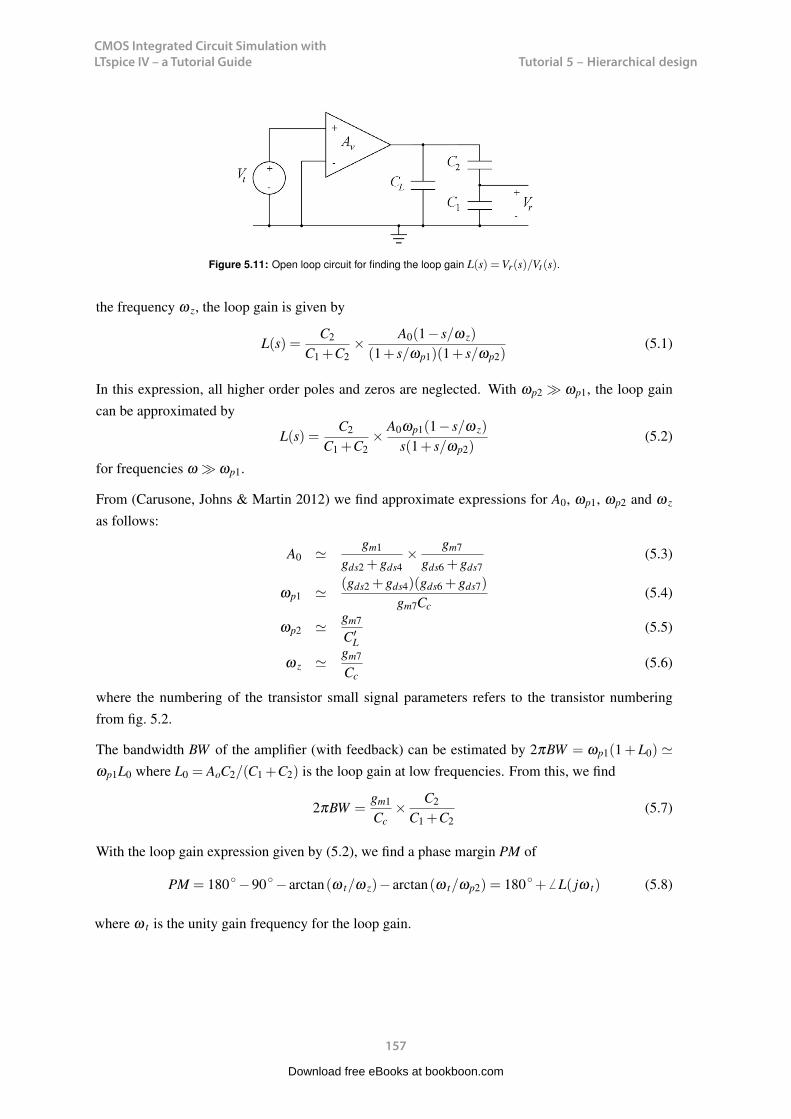
CMOS Integrated Circuit Simulation with LTspice IV – a Tutorial Guide
157
Tutorial 5 – Hierarchical designCMOS Integrated Circuit Simulation with LTspice IV Tutorial 5
Figure 5.11: Open loop circuit for finding the loop gain L(s) =Vr(s)/Vt(s).
the frequency ω z, the loop gain is given by
L(s) =C2
C1 +C2× A0(1− s/ω z)
(1+ s/ωp1)(1+ s/ωp2)(5.1)
In this expression, all higher order poles and zeros are neglected. With ωp2 ωp1, the loop gaincan be approximated by
L(s) =C2
C1 +C2×
A0ωp1(1− s/ω z)
s(1+ s/ωp2)(5.2)
for frequencies ω ωp1.
From (Carusone, Johns & Martin 2012) we find approximate expressions for A0, ωp1, ωp2 and ω z
as follows:
A0 gm1
gds2 +gds4× gm7
gds6 +gds7(5.3)
ωp1 (gds2 +gds4)(gds6 +gds7)
gm7Cc(5.4)
ωp2 gm7
C′L
(5.5)
ω z gm7
Cc(5.6)
where the numbering of the transistor small signal parameters refers to the transistor numberingfrom fig. 5.2.
The bandwidth BW of the amplifier (with feedback) can be estimated by 2πBW = ωp1(1+L0) ωp1L0 where L0 = AoC2/(C1 +C2) is the loop gain at low frequencies. From this, we find
2πBW =gm1
Cc× C2
C1 +C2(5.7)
With the loop gain expression given by (5.2), we find a phase margin PM of
PM = 180 −90 − arctan(ω t/ω z)− arctan(ω t/ωp2) = 180+ L( jω t) (5.8)
157
CMOS Integrated Circuit Simulation with LTspice IV Tutorial 5
where ω t is the unity gain frequency for the loop gain.
We may start by selecting ω z ω t to reduce the influence of the zero. With ω z 10×ω t , thephase shift from the zero is about 6. Also, additional high order poles will contribute to the phaseshift. Assuming (somewhat arbitrarily) an additional phase shift from higher order poles of 4, thisleaves a phase shift of about 15 from the second pole for a phase margin of 65. From this, we get
arctan(ω t/ωp2) = 15 ⇒ ωp2 = 3.8×ω t (5.9)
With the non-dominant pole and the zero well above the unity gain frequency ω t of the loop gain,ω t is approximately given by the gain bandwidth product of the loop gain, i.e.
ω t = L0 ×ωp1 =gm1
Cc× C2
C1 +C2= 2π ·20 MHz (5.10)
Note that the unity gain frequency of the opamp is
ω ta = A0ωp1 = (1+C1/C2)L0ωp1 = 2π ·120 MHz (5.11)
Using ω z = 10×ω t = 2π ·200 MHz in combination with (5.6) and (5.10), we find
gm7
Cc= 10× gm1
Cc× C2
C1 +C2⇒ gm7 =
10×C2
C1 +C2gm1 = 1.67×gm1 (5.12)
From (5.5), (5.9), (5.10) and (5.12) we find
gm7
C′L= 3.8× gm1
Cc× C2
C1 +C2⇒Cc = 0.38×C′
L = 0.63 pF (5.13)
Then, using (5.7) and (5.12) we find
gm1 = 2πBW ×Cc(1+C1/C2) = 0.48 mA/V (5.14)
gm7 = 1.67×gm1 = 0.80 mA/V (5.15)
Next, we consider the slew rate specification. The bias current for M5 is the maximum currentavailable for charging and discharging of Cc, and the bias current for M6 is the maximum current forfor charging the output node when vIN+− vIN− is positive. In this situation, ID6 charges Cc, CL andthe series connection of C1 and C2. From this, we find
SR =ID5
Cc⇒ ID5 ≥ SR×Cc = 19 µA (5.16)
SR =ID6
Cc +CL +C1C2/(C1 +C2)
⇒ ID6 ≥ SR× (Cc +CL +C1C2/(C1 +C2)) = 70 µA (5.17)
158
Download free eBooks at bookboon.com
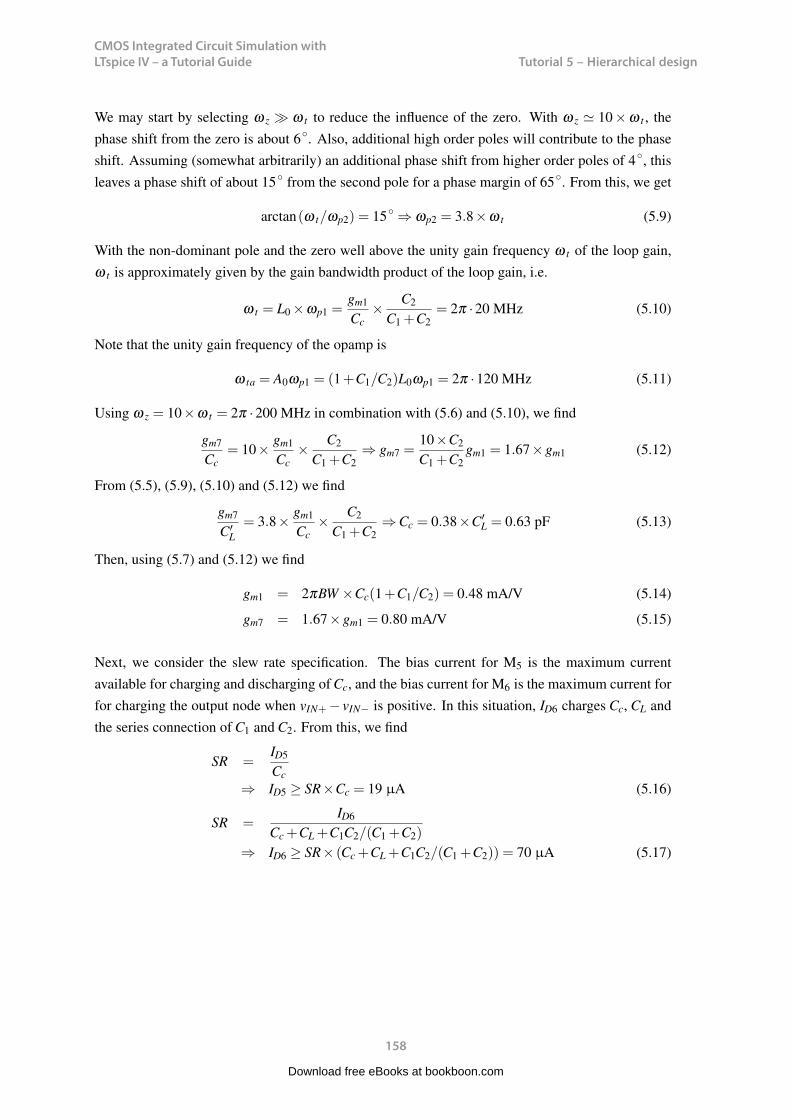
CMOS Integrated Circuit Simulation with LTspice IV – a Tutorial Guide
158
Tutorial 5 – Hierarchical design
CMOS Integrated Circuit Simulation with LTspice IV Tutorial 5
where ω t is the unity gain frequency for the loop gain.
We may start by selecting ω z ω t to reduce the influence of the zero. With ω z 10×ω t , thephase shift from the zero is about 6. Also, additional high order poles will contribute to the phaseshift. Assuming (somewhat arbitrarily) an additional phase shift from higher order poles of 4, thisleaves a phase shift of about 15 from the second pole for a phase margin of 65. From this, we get
arctan(ω t/ωp2) = 15 ⇒ ωp2 = 3.8×ω t (5.9)
With the non-dominant pole and the zero well above the unity gain frequency ω t of the loop gain,ω t is approximately given by the gain bandwidth product of the loop gain, i.e.
ω t = L0 ×ωp1 =gm1
Cc× C2
C1 +C2= 2π ·20 MHz (5.10)
Note that the unity gain frequency of the opamp is
ω ta = A0ωp1 = (1+C1/C2)L0ωp1 = 2π ·120 MHz (5.11)
Using ω z = 10×ω t = 2π ·200 MHz in combination with (5.6) and (5.10), we find
gm7
Cc= 10× gm1
Cc× C2
C1 +C2⇒ gm7 =
10×C2
C1 +C2gm1 = 1.67×gm1 (5.12)
From (5.5), (5.9), (5.10) and (5.12) we find
gm7
C′L= 3.8× gm1
Cc× C2
C1 +C2⇒Cc = 0.38×C′
L = 0.63 pF (5.13)
Then, using (5.7) and (5.12) we find
gm1 = 2πBW ×Cc(1+C1/C2) = 0.48 mA/V (5.14)
gm7 = 1.67×gm1 = 0.80 mA/V (5.15)
Next, we consider the slew rate specification. The bias current for M5 is the maximum currentavailable for charging and discharging of Cc, and the bias current for M6 is the maximum current forfor charging the output node when vIN+− vIN− is positive. In this situation, ID6 charges Cc, CL andthe series connection of C1 and C2. From this, we find
SR =ID5
Cc⇒ ID5 ≥ SR×Cc = 19 µA (5.16)
SR =ID6
Cc +CL +C1C2/(C1 +C2)
⇒ ID6 ≥ SR× (Cc +CL +C1C2/(C1 +C2)) = 70 µA (5.17)
158
Download free eBooks at bookboon.com

CMOS Integrated Circuit Simulation with LTspice IV – a Tutorial Guide
159
Tutorial 5 – Hierarchical designCMOS Integrated Circuit Simulation with LTspice IV Tutorial 5
These values of bias current are minimum values, and it may be a good idea to select somewhatlarger bias current values in order to leave room for design iterations with increased values of Cc.
The bias current for M1 and M2 is obviously ID5/2 and the bias current for M7 is ID7 = ID6, so forM1, M2 and M7 we have found both the transconductances and the minimum bias currents, andusing (3.8) on page 72, the ratio W/L may be found from the Shichman-Hodges transistor model.However, we noticed in tutorial 3 that it is not easy to obtain a good match over a wide range ofvariation in gm between the Shichman-Hodges model and the BSIM3 transistor models specified forthe opamp. So, rather than trying to adapt the Shichman-Hodges parameters to fit the BSIM model,we may use LTspice to find the transconductance gm versus channel width W for the desired valuesof bias current. First, we need to select a value for the channel length, and for this design we chose(somewhat arbitrarily) L to be about three times the minimum dimensions specified for the process,i.e. L = 1 µm for all transistors in the circuit.
In order to simulate gm versus W, we use the approach described in Example 3.6, page 90. As weneed only approximate results and as gm is much larger than gds for the BSIM3 transistors with L= 1µm in the active region, we may just run a ‘.tf’ simulation on a single diode connected transistor asshown in fig. 5.12. For the diode connected transistor, the input resistance is (gm +gds)
−1 1/gm,so stepping W and plotting ‘1/id#input_resistance’ directly shows gm versus W .
159
Download free eBooks at bookboon.com
Click on the ad to read moreClick on the ad to read moreClick on the ad to read moreClick on the ad to read moreClick on the ad to read moreClick on the ad to read moreClick on the ad to read moreClick on the ad to read moreClick on the ad to read moreClick on the ad to read moreClick on the ad to read moreClick on the ad to read moreClick on the ad to read moreClick on the ad to read moreClick on the ad to read moreClick on the ad to read moreClick on the ad to read moreClick on the ad to read moreClick on the ad to read moreClick on the ad to read moreClick on the ad to read moreClick on the ad to read moreClick on the ad to read moreClick on the ad to read moreClick on the ad to read moreClick on the ad to read moreClick on the ad to read moreClick on the ad to read moreClick on the ad to read moreClick on the ad to read moreClick on the ad to read moreClick on the ad to read moreClick on the ad to read moreClick on the ad to read moreClick on the ad to read moreClick on the ad to read moreClick on the ad to read moreClick on the ad to read moreClick on the ad to read moreClick on the ad to read moreClick on the ad to read moreClick on the ad to read moreClick on the ad to read moreClick on the ad to read moreClick on the ad to read moreClick on the ad to read moreClick on the ad to read moreClick on the ad to read moreClick on the ad to read moreClick on the ad to read moreClick on the ad to read moreClick on the ad to read moreClick on the ad to read moreClick on the ad to read moreClick on the ad to read moreClick on the ad to read more
Get Help Now
Go to www.helpmyassignment.co.uk for more info
Need help with yourdissertation?Get in-depth feedback & advice from experts in your topic area. Find out what you can do to improvethe quality of your dissertation!
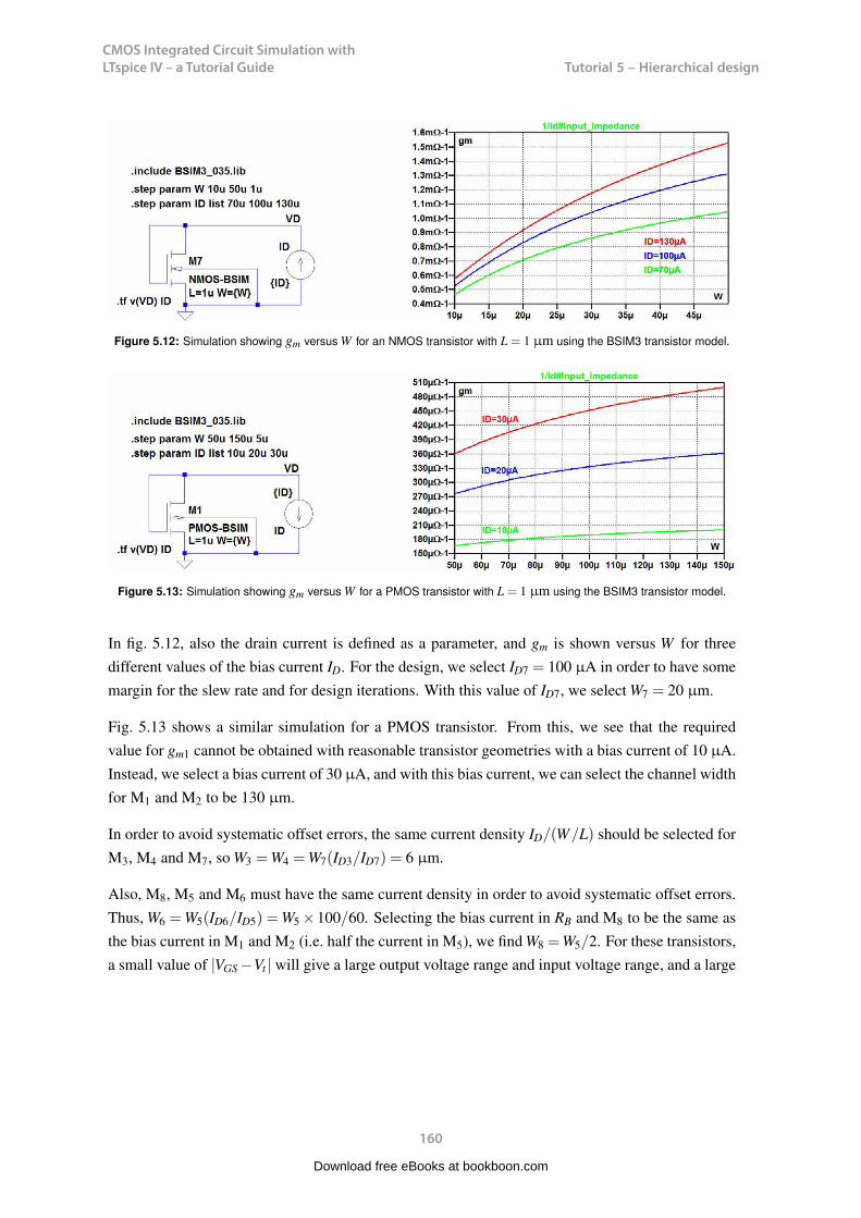
CMOS Integrated Circuit Simulation with LTspice IV – a Tutorial Guide
160
Tutorial 5 – Hierarchical designCMOS Integrated Circuit Simulation with LTspice IV Tutorial 5
Figure 5.12: Simulation showing gm versus W for an NMOS transistor with L = 1 µm using the BSIM3 transistor model.
Figure 5.13: Simulation showing gm versus W for a PMOS transistor with L = 1 µm using the BSIM3 transistor model.
In fig. 5.12, also the drain current is defined as a parameter, and gm is shown versus W for threedifferent values of the bias current ID. For the design, we select ID7 = 100 µA in order to have somemargin for the slew rate and for design iterations. With this value of ID7, we select W7 = 20 µm.
Fig. 5.13 shows a similar simulation for a PMOS transistor. From this, we see that the requiredvalue for gm1 cannot be obtained with reasonable transistor geometries with a bias current of 10 µA.Instead, we select a bias current of 30 µA, and with this bias current, we can select the channel widthfor M1 and M2 to be 130 µm.
In order to avoid systematic offset errors, the same current density ID/(W/L) should be selected forM3, M4 and M7, so W3 =W4 =W7(ID3/ID7) = 6 µm.
Also, M8, M5 and M6 must have the same current density in order to avoid systematic offset errors.Thus, W6 =W5(ID6/ID5) =W5 ×100/60. Selecting the bias current in RB and M8 to be the same asthe bias current in M1 and M2 (i.e. half the current in M5), we find W8 =W5/2. For these transistors,a small value of |VGS −Vt | will give a large output voltage range and input voltage range, and a large
160
Download free eBooks at bookboon.com
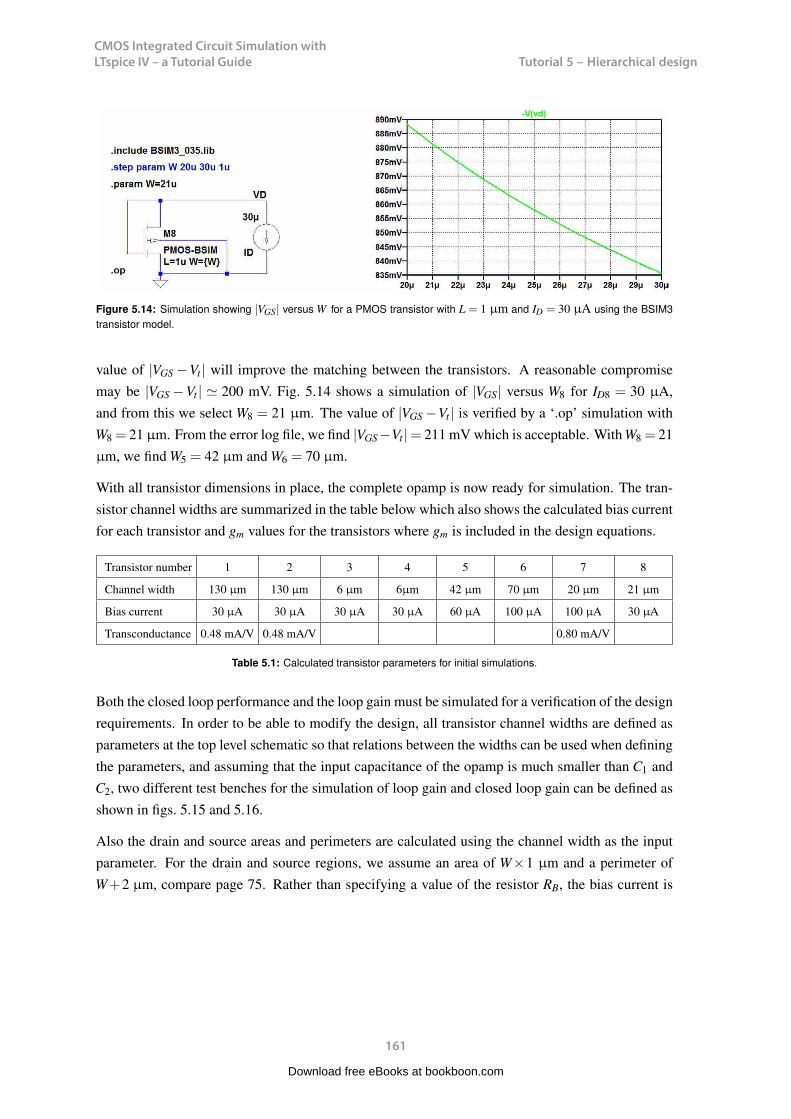
CMOS Integrated Circuit Simulation with LTspice IV – a Tutorial Guide
161
Tutorial 5 – Hierarchical designCMOS Integrated Circuit Simulation with LTspice IV Tutorial 5
Figure 5.14: Simulation showing |VGS| versus W for a PMOS transistor with L = 1 µm and ID = 30 µA using the BSIM3transistor model.
value of |VGS −Vt | will improve the matching between the transistors. A reasonable compromisemay be |VGS −Vt | 200 mV. Fig. 5.14 shows a simulation of |VGS| versus W8 for ID8 = 30 µA,and from this we select W8 = 21 µm. The value of |VGS −Vt | is verified by a ‘.op’ simulation withW8 = 21 µm. From the error log file, we find |VGS−Vt |= 211 mV which is acceptable. With W8 = 21µm, we find W5 = 42 µm and W6 = 70 µm.
With all transistor dimensions in place, the complete opamp is now ready for simulation. The tran-sistor channel widths are summarized in the table below which also shows the calculated bias currentfor each transistor and gm values for the transistors where gm is included in the design equations.
Transistor number 1 2 3 4 5 6 7 8
Channel width 130 µm 130 µm 6 µm 6µm 42 µm 70 µm 20 µm 21 µm
Bias current 30 µA 30 µA 30 µA 30 µA 60 µA 100 µA 100 µA 30 µA
Transconductance 0.48 mA/V 0.48 mA/V 0.80 mA/V
Table 5.1: Calculated transistor parameters for initial simulations.
Both the closed loop performance and the loop gain must be simulated for a verification of the designrequirements. In order to be able to modify the design, all transistor channel widths are defined asparameters at the top level schematic so that relations between the widths can be used when definingthe parameters, and assuming that the input capacitance of the opamp is much smaller than C1 andC2, two different test benches for the simulation of loop gain and closed loop gain can be defined asshown in figs. 5.15 and 5.16.
Also the drain and source areas and perimeters are calculated using the channel width as the inputparameter. For the drain and source regions, we assume an area of W×1 µm and a perimeter ofW+2 µm, compare page 75. Rather than specifying a value of the resistor RB, the bias current is
161
Download free eBooks at bookboon.com
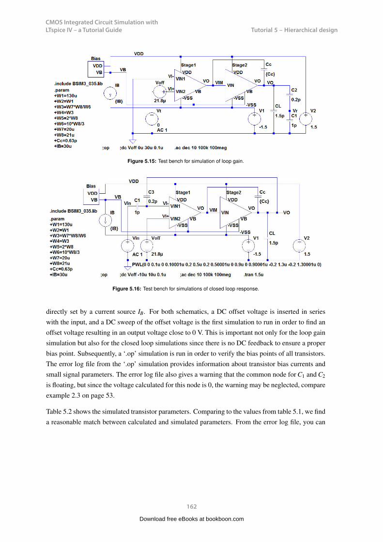
CMOS Integrated Circuit Simulation with LTspice IV – a Tutorial Guide
162
Tutorial 5 – Hierarchical designCMOS Integrated Circuit Simulation with LTspice IV Tutorial 5
Figure 5.15: Test bench for simulation of loop gain.
Figure 5.16: Test bench for simulations of closed loop response.
directly set by a current source IB. For both schematics, a DC offset voltage is inserted in serieswith the input, and a DC sweep of the offset voltage is the first simulation to run in order to find anoffset voltage resulting in an output voltage close to 0 V. This is important not only for the loop gainsimulation but also for the closed loop simulations since there is no DC feedback to ensure a properbias point. Subsequently, a ‘.op’ simulation is run in order to verify the bias points of all transistors.The error log file from the ‘.op’ simulation provides information about transistor bias currents andsmall signal parameters. The error log file also gives a warning that the common node for C1 and C2
is floating, but since the voltage calculated for this node is 0, the warning may be neglected, compareexample 2.3 on page 53.
Table 5.2 shows the simulated transistor parameters. Comparing to the values from table 5.1, we finda reasonable match between calculated and simulated parameters. From the error log file, you can
162
Download free eBooks at bookboon.com

CMOS Integrated Circuit Simulation with LTspice IV – a Tutorial Guide
163
Tutorial 5 – Hierarchical designCMOS Integrated Circuit Simulation with LTspice IV Tutorial 5
Transistor number 1 2 3 4 5 6 7 8
Channel width 130 µm 130 µm 6 µm 6 µm 42 µm 70 µm 20 µm 21 µm
Bias current 31.80 µA 31.8 µA 31.8 µA 31.8 µA 63.5 µA 119 µA 119 µA 30 µA
Transconductance 0.51 mA/V 0.51 mA/V 0.89 mA/V
Table 5.2: Simulated transistor parameters from the initial ‘.op’ simulation of fig. 5.15.
also find the parasitic transistor capacitances calculated on basis of the transistor dimensions. Theyare all much smaller than C1, C2 and Cc but some of them on the order of 0.1pF can be expectedto affect the position of the zero and the second pole and also introduce additional pole(s) from theinput stage. This will cause an additional phase shift of the loop gain.
After having verified the bias point, a ‘.ac’ simulation is run to find the loop gain and the phasemargin. Fig. 5.17(a) shows the resulting gain and phase response of the loop gain L( jω) or ‘V(vr)’.Fig. 5.17(b) shows a Bode plot of −L( jω) or ‘-V(vr)’. Since (−L( jω)) = 180+ L( jω) = PMfor ω = ω t , this plot directly shows the phase margin at the frequency where the amplitude is 0 dB.From these plots, we find a phase margin of 61 which is slightly lower than the design specification.Before modifying the design, we also run a ‘.ac’ simulation and a ‘.tran’ simulation of the closedloop circuit, fig. 5.16, in order to find the bandwidth and the slew rate of the amplifier with feedback.The results of these simulations are shown in fig. 5.18, and we notice a bandwidth of 26.8 MHz and
163
Download free eBooks at bookboon.com
Click on the ad to read moreClick on the ad to read moreClick on the ad to read moreClick on the ad to read moreClick on the ad to read moreClick on the ad to read moreClick on the ad to read moreClick on the ad to read moreClick on the ad to read moreClick on the ad to read moreClick on the ad to read moreClick on the ad to read moreClick on the ad to read moreClick on the ad to read moreClick on the ad to read moreClick on the ad to read moreClick on the ad to read moreClick on the ad to read moreClick on the ad to read moreClick on the ad to read moreClick on the ad to read moreClick on the ad to read moreClick on the ad to read moreClick on the ad to read moreClick on the ad to read moreClick on the ad to read moreClick on the ad to read moreClick on the ad to read moreClick on the ad to read moreClick on the ad to read moreClick on the ad to read moreClick on the ad to read moreClick on the ad to read moreClick on the ad to read moreClick on the ad to read moreClick on the ad to read moreClick on the ad to read moreClick on the ad to read moreClick on the ad to read moreClick on the ad to read moreClick on the ad to read moreClick on the ad to read moreClick on the ad to read moreClick on the ad to read moreClick on the ad to read moreClick on the ad to read moreClick on the ad to read moreClick on the ad to read moreClick on the ad to read moreClick on the ad to read moreClick on the ad to read moreClick on the ad to read moreClick on the ad to read moreClick on the ad to read moreClick on the ad to read moreClick on the ad to read moreClick on the ad to read more
By 2020, wind could provide one-tenth of our planet’s electricity needs. Already today, SKF’s innovative know-how is crucial to running a large proportion of the world’s wind turbines.
Up to 25 % of the generating costs relate to mainte-nance. These can be reduced dramatically thanks to our systems for on-line condition monitoring and automatic lubrication. We help make it more economical to create cleaner, cheaper energy out of thin air.
By sharing our experience, expertise, and creativity, industries can boost performance beyond expectations.
Therefore we need the best employees who can meet this challenge!
The Power of Knowledge Engineering
Brain power
Plug into The Power of Knowledge Engineering.
Visit us at www.skf.com/knowledge
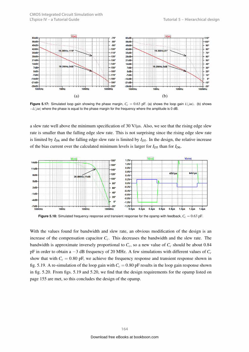
CMOS Integrated Circuit Simulation with LTspice IV – a Tutorial Guide
164
Tutorial 5 – Hierarchical designCMOS Integrated Circuit Simulation with LTspice IV Tutorial 5
(a) (b)
Figure 5.17: Simulated loop gain showing the phase margin, Cc = 0.63 pF. (a) shows the loop gain L( jω). (b) shows−L( jω) where the phase is equal to the phase margin for the frequency where the amplitude is 0 dB.
a slew rate well above the minimum specification of 30 V/µs. Also, we see that the rising edge slewrate is smaller than the falling edge slew rate. This is not surprising since the rising edge slew rateis limited by ID6 and the falling edge slew rate is limited by ID5. In the design, the relative increaseof the bias current over the calculated minimum levels is larger for ID5 than for ID6.
Figure 5.18: Simulated frequency response and transient response for the opamp with feedback, Cc = 0.63 pF.
With the values found for bandwidth and slew rate, an obvious modification of the design is anincrease of the compensation capacitor Cc. This decreases the bandwidth and the slew rate. Thebandwidth is approximate inversely proportional to Cc, so a new value of Cc should be about 0.84pF in order to obtain a −3 dB frequency of 20 MHz. A few simulations with different values of Cc
show that with Cc = 0.80 pF, we achieve the frequency response and transient response shown infig. 5.19. A re-simulation of the loop gain with Cc = 0.80 pF results in the loop gain response shownin fig. 5.20. From figs. 5.19 and 5.20, we find that the design requirements for the opamp listed onpage 155 are met, so this concludes the design of the opamp.
164
Download free eBooks at bookboon.com
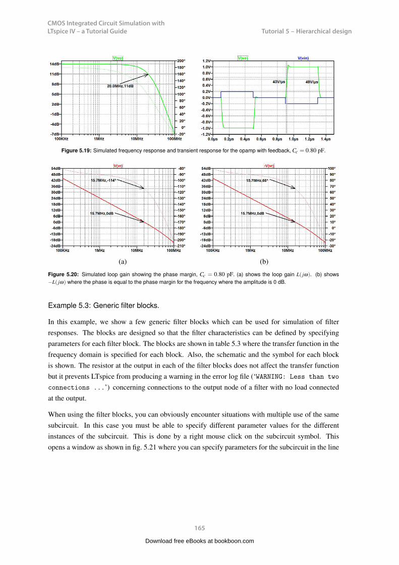
CMOS Integrated Circuit Simulation with LTspice IV – a Tutorial Guide
165
Tutorial 5 – Hierarchical designCMOS Integrated Circuit Simulation with LTspice IV Tutorial 5
Figure 5.19: Simulated frequency response and transient response for the opamp with feedback, Cc = 0.80 pF.
(a) (b)
Figure 5.20: Simulated loop gain showing the phase margin, Cc = 0.80 pF. (a) shows the loop gain L( jω). (b) shows−L( jω) where the phase is equal to the phase margin for the frequency where the amplitude is 0 dB.
Example 5.3: Generic filter blocks.
In this example, we show a few generic filter blocks which can be used for simulation of filterresponses. The blocks are designed so that the filter characteristics can be defined by specifyingparameters for each filter block. The blocks are shown in table 5.3 where the transfer function in thefrequency domain is specified for each block. Also, the schematic and the symbol for each blockis shown. The resistor at the output in each of the filter blocks does not affect the transfer functionbut it prevents LTspice from producing a warning in the error log file (‘WARNING: Less than two
connections ...’) concerning connections to the output node of a filter with no load connectedat the output.
When using the filter blocks, you can obviously encounter situations with multiple use of the samesubcircuit. In this case you must be able to specify different parameter values for the differentinstances of the subcircuit. This is done by a right mouse click on the subcircuit symbol. Thisopens a window as shown in fig. 5.21 where you can specify parameters for the subcircuit in the line
165
Download free eBooks at bookboon.com
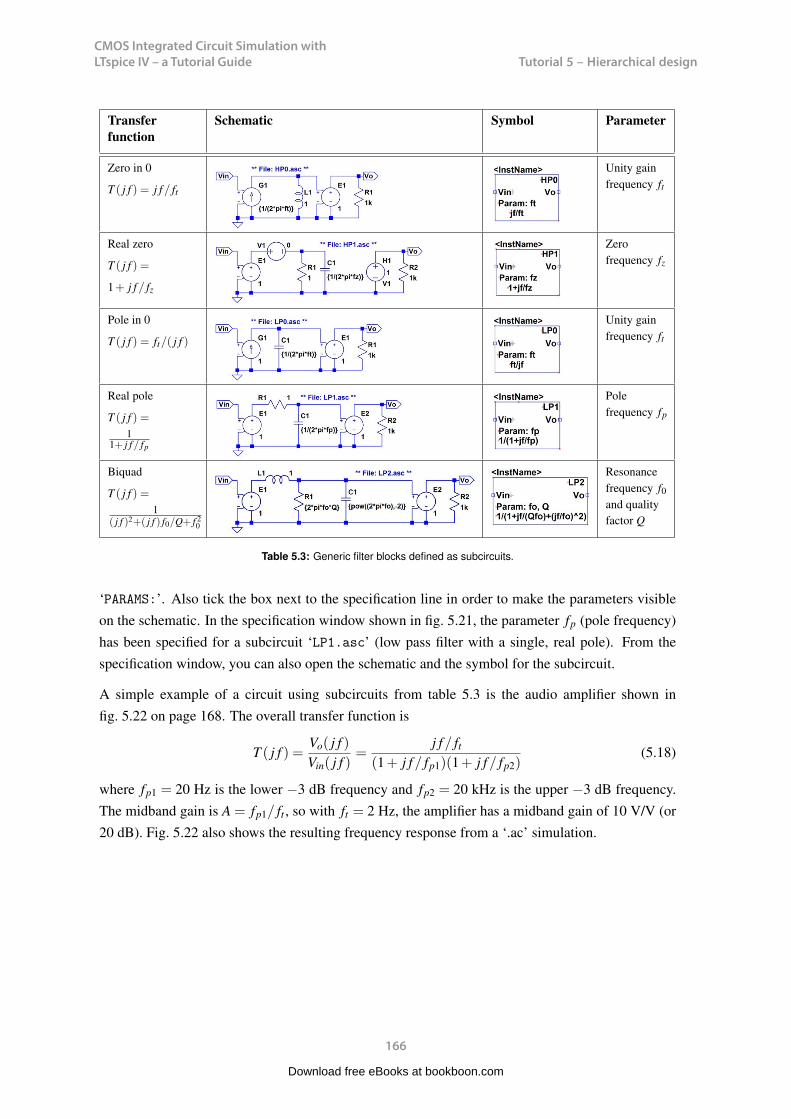
CMOS Integrated Circuit Simulation with LTspice IV – a Tutorial Guide
166
Tutorial 5 – Hierarchical designCMOS Integrated Circuit Simulation with LTspice IV Tutorial 5
Transferfunction
Schematic Symbol Parameter
Zero in 0
T ( j f ) = j f/ ft
Unity gainfrequency ft
Real zero
T ( j f ) =
1+ j f/ fz
Zerofrequency fz
Pole in 0
T ( j f ) = ft/( j f )
Unity gainfrequency ft
Real pole
T ( j f ) =1
1+ j f/ fp
Polefrequency fp
Biquad
T ( j f ) =1
( j f )2+( j f ) f0/Q+ f 20
Resonancefrequency f0and qualityfactor Q
Table 5.3: Generic filter blocks defined as subcircuits.
‘PARAMS:’. Also tick the box next to the specification line in order to make the parameters visibleon the schematic. In the specification window shown in fig. 5.21, the parameter fp (pole frequency)has been specified for a subcircuit ‘LP1.asc’ (low pass filter with a single, real pole). From thespecification window, you can also open the schematic and the symbol for the subcircuit.
A simple example of a circuit using subcircuits from table 5.3 is the audio amplifier shown infig. 5.22 on page 168. The overall transfer function is
T ( j f ) =Vo( j f )Vin( j f )
=j f/ ft
(1+ j f/ fp1)(1+ j f/ fp2)(5.18)
where fp1 = 20 Hz is the lower −3 dB frequency and fp2 = 20 kHz is the upper −3 dB frequency.The midband gain is A = fp1/ ft , so with ft = 2 Hz, the amplifier has a midband gain of 10 V/V (or20 dB). Fig. 5.22 also shows the resulting frequency response from a ‘.ac’ simulation.
The filter blocks shown in table 5.3 are also very suitable for the investigation of a feedback amplifieras designed in Example 5.2 (page 154). From (5.2), we find that the transfer function of the amplifier
166
Download free eBooks at bookboon.com
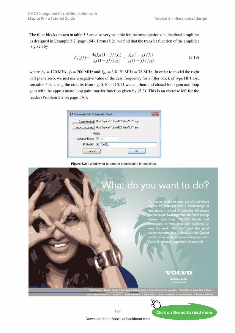
CMOS Integrated Circuit Simulation with LTspice IV – a Tutorial Guide
167
Tutorial 5 – Hierarchical design
CMOS Integrated Circuit Simulation with LTspice IV Tutorial 5
is given by
Av( j f ) =A0 fp1(1− j f/ fz)
j f (1+ j f/ fp2)=
fta(1− j f/ fz)
j f (1+ j f/ fp2)(5.19)
where fta = 120 MHz, fz = 200 MHz and fp2 = 3.8 ·20 MHz = 76 MHz. In order to model the righthalf plane zero, we just use a negative value of the zero frequency for a filter block of type HP1.asc,see table 5.3. Using the circuits from fig. 5.10 and 5.11 we can then find closed loop gain and loopgain with the approximate loop gain transfer function given by (5.2). This is an exercise left for thereader (Problem 5.2 on page 176).
Figure 5.21: Window for parameter specification for subcircuit.
167
CMOS Integrated Circuit Simulation with LTspice IV Tutorial 5
Transferfunction
Schematic Symbol Parameter
Zero in 0
T ( j f ) = j f/ ft
Unity gainfrequency ft
Real zero
T ( j f ) =
1+ j f/ fz
Zerofrequency fz
Pole in 0
T ( j f ) = ft/( j f )
Unity gainfrequency ft
Real pole
T ( j f ) =1
1+ j f/ fp
Polefrequency fp
Biquad
T ( j f ) =1
( j f )2+( j f ) f0/Q+ f 20
Resonancefrequency f0and qualityfactor Q
Table 5.3: Generic filter blocks defined as subcircuits.
‘PARAMS:’. Also tick the box next to the specification line in order to make the parameters visibleon the schematic. In the specification window shown in fig. 5.21, the parameter fp (pole frequency)has been specified for a subcircuit ‘LP1.asc’ (low pass filter with a single, real pole). From thespecification window, you can also open the schematic and the symbol for the subcircuit.
A simple example of a circuit using subcircuits from table 5.3 is the audio amplifier shown infig. 5.22 on page 168. The overall transfer function is
T ( j f ) =Vo( j f )Vin( j f )
=j f/ ft
(1+ j f/ fp1)(1+ j f/ fp2)(5.18)
where fp1 = 20 Hz is the lower −3 dB frequency and fp2 = 20 kHz is the upper −3 dB frequency.The midband gain is A = fp1/ ft , so with ft = 2 Hz, the amplifier has a midband gain of 10 V/V (or20 dB). Fig. 5.22 also shows the resulting frequency response from a ‘.ac’ simulation.
The filter blocks shown in table 5.3 are also very suitable for the investigation of a feedback amplifieras designed in Example 5.2 (page 154). From (5.2), we find that the transfer function of the amplifier
166
Download free eBooks at bookboon.com
Click on the ad to read moreClick on the ad to read moreClick on the ad to read moreClick on the ad to read moreClick on the ad to read moreClick on the ad to read moreClick on the ad to read moreClick on the ad to read moreClick on the ad to read moreClick on the ad to read moreClick on the ad to read moreClick on the ad to read moreClick on the ad to read moreClick on the ad to read moreClick on the ad to read moreClick on the ad to read moreClick on the ad to read moreClick on the ad to read moreClick on the ad to read moreClick on the ad to read moreClick on the ad to read moreClick on the ad to read moreClick on the ad to read moreClick on the ad to read moreClick on the ad to read moreClick on the ad to read moreClick on the ad to read moreClick on the ad to read moreClick on the ad to read moreClick on the ad to read moreClick on the ad to read moreClick on the ad to read moreClick on the ad to read moreClick on the ad to read moreClick on the ad to read moreClick on the ad to read moreClick on the ad to read moreClick on the ad to read moreClick on the ad to read moreClick on the ad to read moreClick on the ad to read moreClick on the ad to read moreClick on the ad to read moreClick on the ad to read moreClick on the ad to read moreClick on the ad to read moreClick on the ad to read moreClick on the ad to read moreClick on the ad to read moreClick on the ad to read moreClick on the ad to read moreClick on the ad to read moreClick on the ad to read moreClick on the ad to read moreClick on the ad to read moreClick on the ad to read moreClick on the ad to read moreClick on the ad to read more
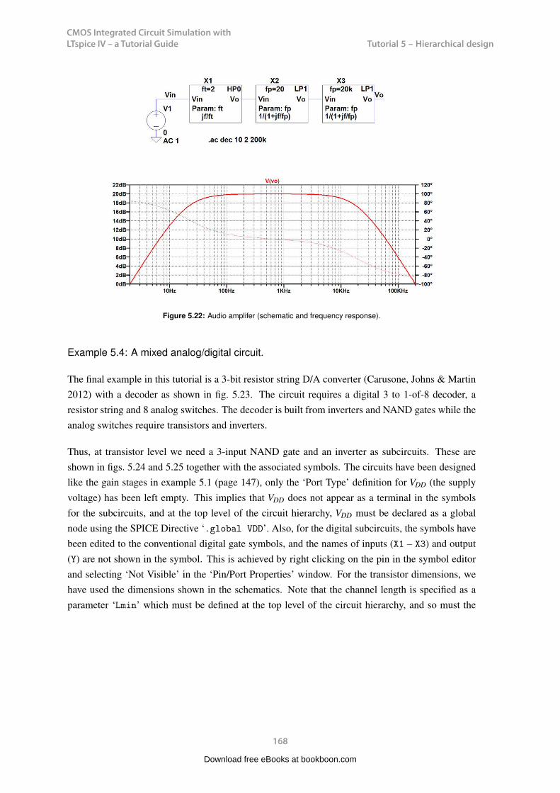
CMOS Integrated Circuit Simulation with LTspice IV – a Tutorial Guide
168
Tutorial 5 – Hierarchical design
CMOS Integrated Circuit Simulation with LTspice IV Tutorial 5
Figure 5.22: Audio amplifer (schematic and frequency response).
Example 5.4: A mixed analog/digital circuit.
The final example in this tutorial is a 3-bit resistor string D/A converter (Carusone, Johns & Martin2012) with a decoder as shown in fig. 5.23. The circuit requires a digital 3 to 1-of-8 decoder, aresistor string and 8 analog switches. The decoder is built from inverters and NAND gates while theanalog switches require transistors and inverters.
Thus, at transistor level we need a 3-input NAND gate and an inverter as subcircuits. These areshown in figs. 5.24 and 5.25 together with the associated symbols. The circuits have been designedlike the gain stages in example 5.1 (page 147), only the ‘Port Type’ definition for VDD (the supplyvoltage) has been left empty. This implies that VDD does not appear as a terminal in the symbolsfor the subcircuits, and at the top level of the circuit hierarchy, VDD must be declared as a globalnode using the SPICE Directive ‘.global VDD’. Also, for the digital subcircuits, the symbols havebeen edited to the conventional digital gate symbols, and the names of inputs (X1 – X3) and output(Y) are not shown in the symbol. This is achieved by right clicking on the pin in the symbol editorand selecting ‘Not Visible’ in the ‘Pin/Port Properties’ window. For the transistor dimensions, wehave used the dimensions shown in the schematics. Note that the channel length is specified as aparameter ‘Lmin’ which must be defined at the top level of the circuit hierarchy, and so must the
168
Download free eBooks at bookboon.com
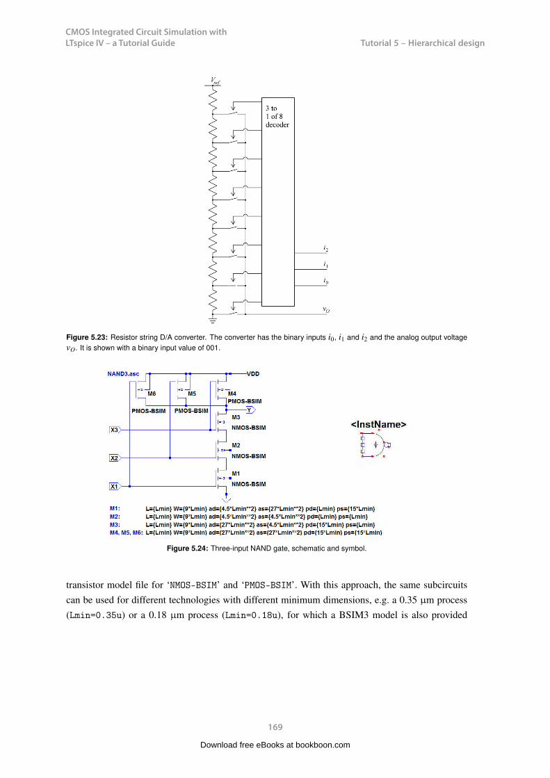
CMOS Integrated Circuit Simulation with LTspice IV – a Tutorial Guide
169
Tutorial 5 – Hierarchical designCMOS Integrated Circuit Simulation with LTspice IV Tutorial 5
Figure 5.23: Resistor string D/A converter. The converter has the binary inputs i0, i1 and i2 and the analog output voltagevO. It is shown with a binary input value of 001.
Figure 5.24: Three-input NAND gate, schematic and symbol.
transistor model file for ‘NMOS-BSIM’ and ‘PMOS-BSIM’. With this approach, the same subcircuitscan be used for different technologies with different minimum dimensions, e.g. a 0.35 µm process(Lmin=0.35u) or a 0.18 µm process (Lmin=0.18u), for which a BSIM3 model is also provided
169
Download free eBooks at bookboon.com

CMOS Integrated Circuit Simulation with LTspice IV – a Tutorial Guide
170
Tutorial 5 – Hierarchical designCMOS Integrated Circuit Simulation with LTspice IV Tutorial 5
Figure 5.25: Inverter, schematic and symbol.
in (Carusone, Johns & Martin 2014). More examples of model files for different values of ‘Lmin’can be found in (Baker 2010) and in (The MOSIS Service: Wafer Electrical Test Data and SPICEModel Parameters 2014). Additionally, transistor widths have been scaled for PMOS and NMOStransistors to compensate for the difference in hole mobility µp and electron mobility µn.
For the inverter, an additional parameter ‘Fanout’ has been used. With this parameter, the transistordimensions in the inverter can be scaled when the inverter is used as a buffer driving a large numberof inputs or a large capacitive load. The default parameter Fanout=1 is defined in the invertersubcircuit. When a different value of Fanout is required, it is specified when inserting the inverterin the higher level schematic using the specification window shown in fig. 5.21 on page 167. This
170
CMOS Integrated Circuit Simulation with LTspice IV Tutorial 5
specification will override the specification given in fig. 5.25.
With these subcircuits defined, the decoder and the analog switch are easily designed as shown infigs. 5.26 and 5.27. As the decoder has an active low output, the analog switch has been designed tohave an active low input, indicated by a small circle in the symbols.
Finally, the complete D/A converter is shown in fig. 5.28. The circuit has three levels of hierarchy.The supply voltage is inserted as shown at the top level of the hierarchy with the command ‘.global
Figure 5.26: Analog switch, schematic and symbol.
Figure 5.27: 1 to 1-of-8 decoder, schematic and symbol.
171
Download free eBooks at bookboon.com
Click on the ad to read moreClick on the ad to read moreClick on the ad to read moreClick on the ad to read moreClick on the ad to read moreClick on the ad to read moreClick on the ad to read moreClick on the ad to read moreClick on the ad to read moreClick on the ad to read moreClick on the ad to read moreClick on the ad to read moreClick on the ad to read moreClick on the ad to read moreClick on the ad to read moreClick on the ad to read moreClick on the ad to read moreClick on the ad to read moreClick on the ad to read moreClick on the ad to read moreClick on the ad to read moreClick on the ad to read moreClick on the ad to read moreClick on the ad to read moreClick on the ad to read moreClick on the ad to read moreClick on the ad to read moreClick on the ad to read moreClick on the ad to read moreClick on the ad to read moreClick on the ad to read moreClick on the ad to read moreClick on the ad to read moreClick on the ad to read moreClick on the ad to read moreClick on the ad to read moreClick on the ad to read moreClick on the ad to read moreClick on the ad to read moreClick on the ad to read moreClick on the ad to read moreClick on the ad to read moreClick on the ad to read moreClick on the ad to read moreClick on the ad to read moreClick on the ad to read moreClick on the ad to read moreClick on the ad to read moreClick on the ad to read moreClick on the ad to read moreClick on the ad to read moreClick on the ad to read moreClick on the ad to read moreClick on the ad to read moreClick on the ad to read moreClick on the ad to read moreClick on the ad to read moreClick on the ad to read moreClick on the ad to read more
EXPERIENCE THE POWER OF FULL ENGAGEMENT…
RUN FASTER. RUN LONGER.. RUN EASIER…
READ MORE & PRE-ORDER TODAY WWW.GAITEYE.COM
Challenge the way we run
1349906_A6_4+0.indd 1 22-08-2014 12:56:57
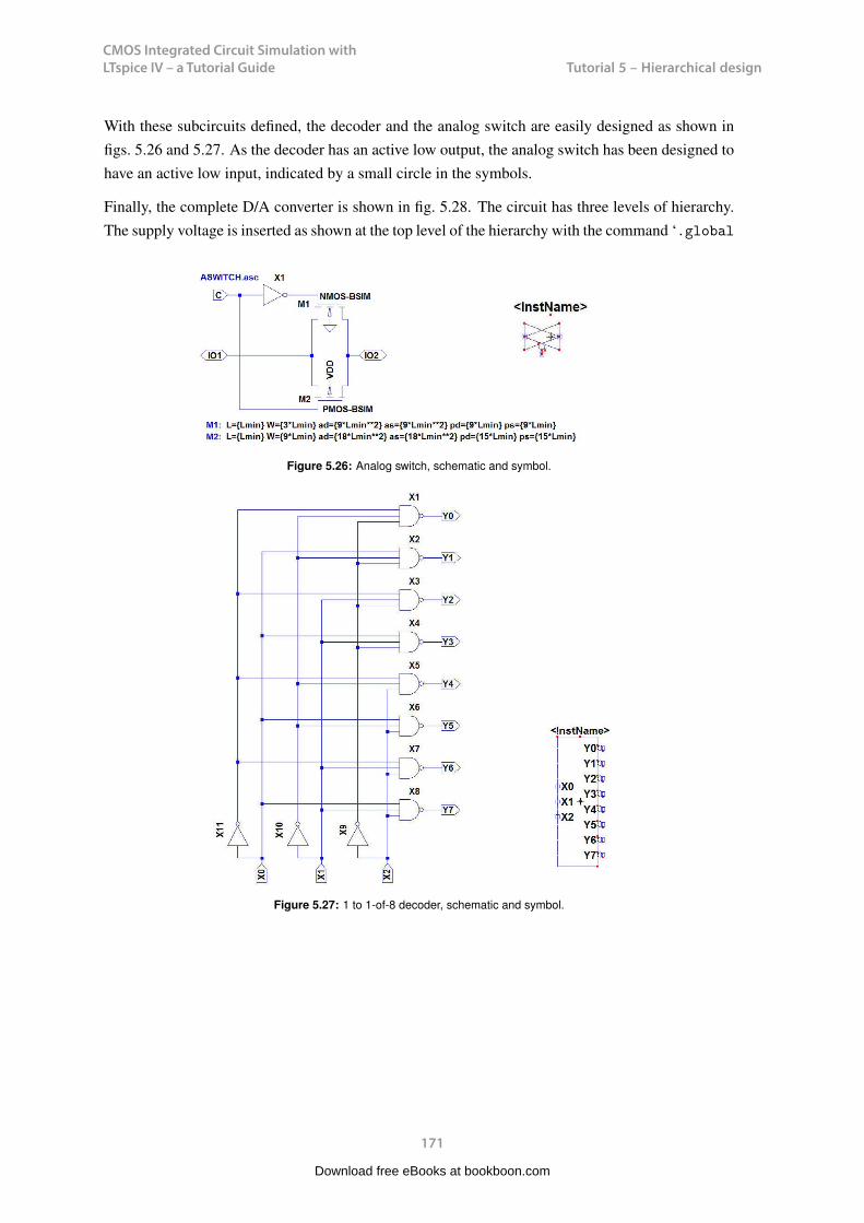
CMOS Integrated Circuit Simulation with LTspice IV – a Tutorial Guide
171
Tutorial 5 – Hierarchical design
CMOS Integrated Circuit Simulation with LTspice IV Tutorial 5
specification will override the specification given in fig. 5.25.
With these subcircuits defined, the decoder and the analog switch are easily designed as shown infigs. 5.26 and 5.27. As the decoder has an active low output, the analog switch has been designed tohave an active low input, indicated by a small circle in the symbols.
Finally, the complete D/A converter is shown in fig. 5.28. The circuit has three levels of hierarchy.The supply voltage is inserted as shown at the top level of the hierarchy with the command ‘.global
Figure 5.26: Analog switch, schematic and symbol.
Figure 5.27: 1 to 1-of-8 decoder, schematic and symbol.
171
Download free eBooks at bookboon.com
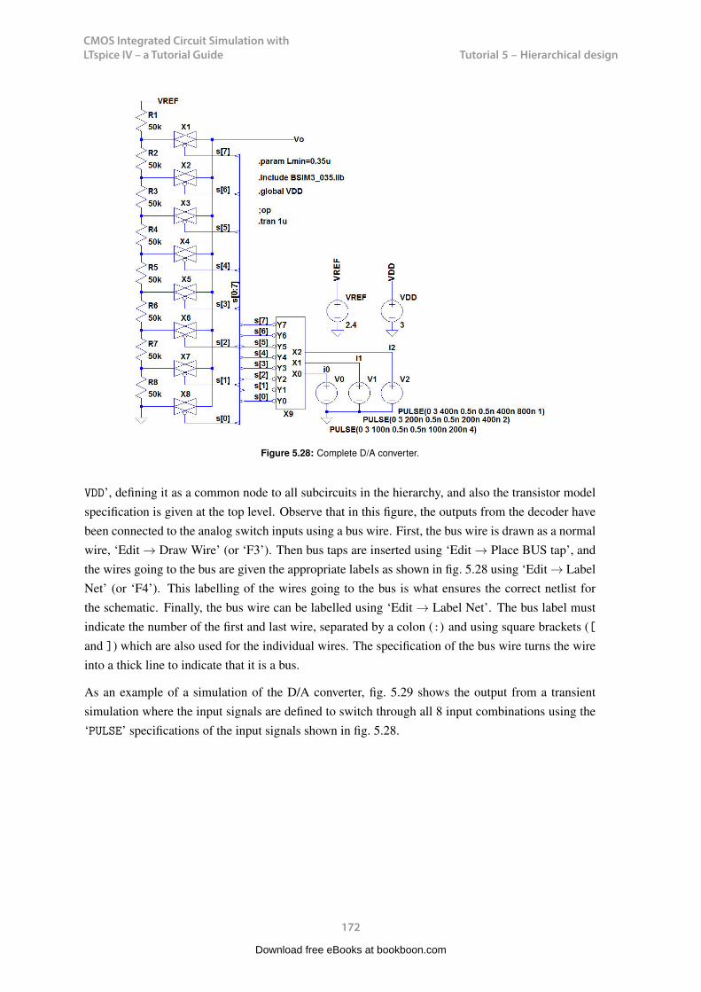
CMOS Integrated Circuit Simulation with LTspice IV – a Tutorial Guide
172
Tutorial 5 – Hierarchical designCMOS Integrated Circuit Simulation with LTspice IV Tutorial 5
Figure 5.28: Complete D/A converter.
VDD’, defining it as a common node to all subcircuits in the hierarchy, and also the transistor modelspecification is given at the top level. Observe that in this figure, the outputs from the decoder havebeen connected to the analog switch inputs using a bus wire. First, the bus wire is drawn as a normalwire, ‘Edit → Draw Wire’ (or ‘F3’). Then bus taps are inserted using ‘Edit → Place BUS tap’, andthe wires going to the bus are given the appropriate labels as shown in fig. 5.28 using ‘Edit → LabelNet’ (or ‘F4’). This labelling of the wires going to the bus is what ensures the correct netlist forthe schematic. Finally, the bus wire can be labelled using ‘Edit → Label Net’. The bus label mustindicate the number of the first and last wire, separated by a colon (:) and using square brackets ([and ]) which are also used for the individual wires. The specification of the bus wire turns the wireinto a thick line to indicate that it is a bus.
As an example of a simulation of the D/A converter, fig. 5.29 shows the output from a transientsimulation where the input signals are defined to switch through all 8 input combinations using the‘PULSE’ specifications of the input signals shown in fig. 5.28.
172
Download free eBooks at bookboon.com
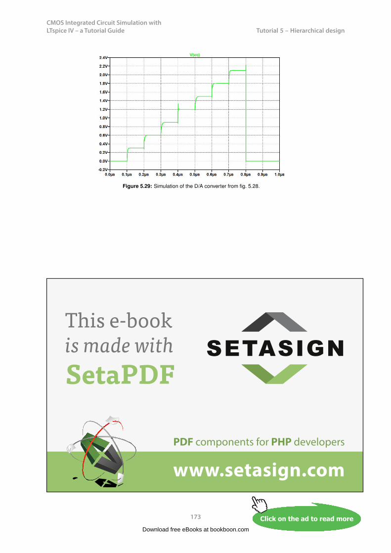
CMOS Integrated Circuit Simulation with LTspice IV – a Tutorial Guide
173
Tutorial 5 – Hierarchical designCMOS Integrated Circuit Simulation with LTspice IV Tutorial 5
Figure 5.29: Simulation of the D/A converter from fig. 5.28.
173
Download free eBooks at bookboon.com
Click on the ad to read moreClick on the ad to read moreClick on the ad to read moreClick on the ad to read moreClick on the ad to read moreClick on the ad to read moreClick on the ad to read moreClick on the ad to read moreClick on the ad to read moreClick on the ad to read moreClick on the ad to read moreClick on the ad to read moreClick on the ad to read moreClick on the ad to read moreClick on the ad to read moreClick on the ad to read moreClick on the ad to read moreClick on the ad to read moreClick on the ad to read moreClick on the ad to read moreClick on the ad to read moreClick on the ad to read moreClick on the ad to read moreClick on the ad to read moreClick on the ad to read moreClick on the ad to read moreClick on the ad to read moreClick on the ad to read moreClick on the ad to read moreClick on the ad to read moreClick on the ad to read moreClick on the ad to read moreClick on the ad to read moreClick on the ad to read moreClick on the ad to read moreClick on the ad to read moreClick on the ad to read moreClick on the ad to read moreClick on the ad to read moreClick on the ad to read moreClick on the ad to read moreClick on the ad to read moreClick on the ad to read moreClick on the ad to read moreClick on the ad to read moreClick on the ad to read moreClick on the ad to read moreClick on the ad to read moreClick on the ad to read moreClick on the ad to read moreClick on the ad to read moreClick on the ad to read moreClick on the ad to read moreClick on the ad to read moreClick on the ad to read moreClick on the ad to read moreClick on the ad to read moreClick on the ad to read moreClick on the ad to read moreClick on the ad to read more
PDF components for PHP developers
www.setasign.com
SETASIGNThis e-book is made with SetaPDF
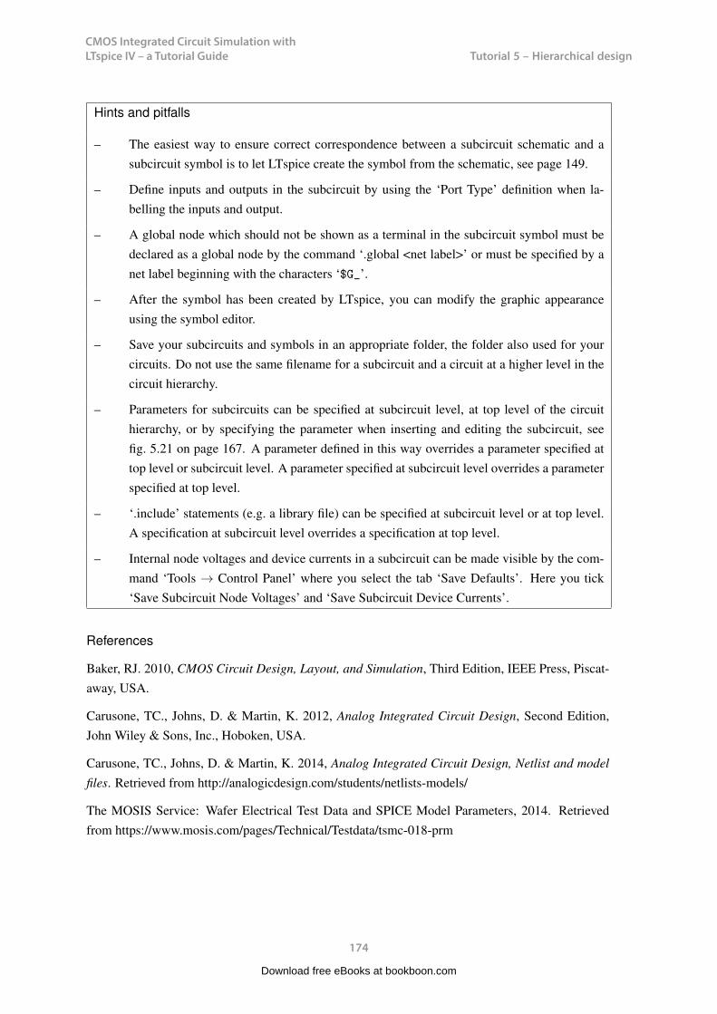
CMOS Integrated Circuit Simulation with LTspice IV – a Tutorial Guide
174
Tutorial 5 – Hierarchical designCMOS Integrated Circuit Simulation with LTspice IV Tutorial 5
Hints and pitfalls
– The easiest way to ensure correct correspondence between a subcircuit schematic and asubcircuit symbol is to let LTspice create the symbol from the schematic, see page 149.
– Define inputs and outputs in the subcircuit by using the ‘Port Type’ definition when la-belling the inputs and output.
– A global node which should not be shown as a terminal in the subcircuit symbol must bedeclared as a global node by the command ‘.global <net label>’ or must be specified by anet label beginning with the characters ‘$G_’.
– After the symbol has been created by LTspice, you can modify the graphic appearanceusing the symbol editor.
– Save your subcircuits and symbols in an appropriate folder, the folder also used for yourcircuits. Do not use the same filename for a subcircuit and a circuit at a higher level in thecircuit hierarchy.
– Parameters for subcircuits can be specified at subcircuit level, at top level of the circuithierarchy, or by specifying the parameter when inserting and editing the subcircuit, seefig. 5.21 on page 167. A parameter defined in this way overrides a parameter specified attop level or subcircuit level. A parameter specified at subcircuit level overrides a parameterspecified at top level.
– ‘.include’ statements (e.g. a library file) can be specified at subcircuit level or at top level.A specification at subcircuit level overrides a specification at top level.
– Internal node voltages and device currents in a subcircuit can be made visible by the com-mand ‘Tools → Control Panel’ where you select the tab ‘Save Defaults’. Here you tick‘Save Subcircuit Node Voltages’ and ‘Save Subcircuit Device Currents’.
References
Baker, RJ. 2010, CMOS Circuit Design, Layout, and Simulation, Third Edition, IEEE Press, Piscat-away, USA.
Carusone, TC., Johns, D. & Martin, K. 2012, Analog Integrated Circuit Design, Second Edition,John Wiley & Sons, Inc., Hoboken, USA.
Carusone, TC., Johns, D. & Martin, K. 2014, Analog Integrated Circuit Design, Netlist and modelfiles. Retrieved from http://analogicdesign.com/students/netlists-models/
The MOSIS Service: Wafer Electrical Test Data and SPICE Model Parameters, 2014. Retrievedfrom https://www.mosis.com/pages/Technical/Testdata/tsmc-018-prm
174
Download free eBooks at bookboon.com
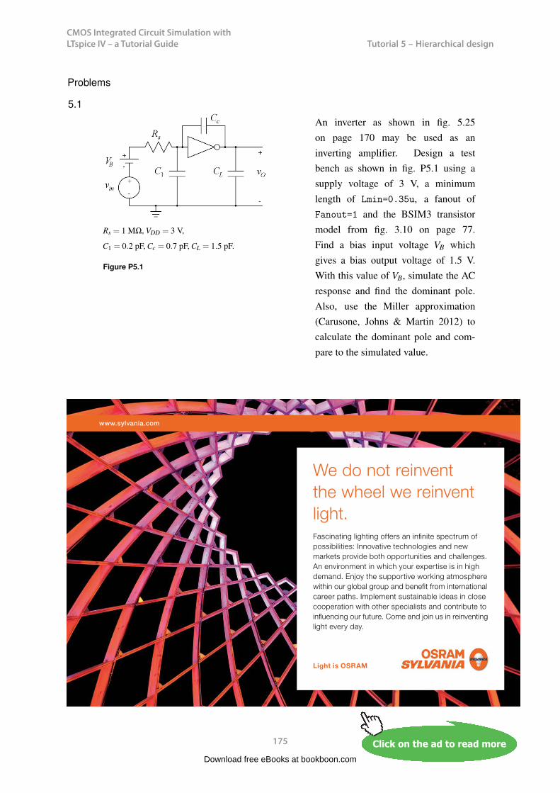
CMOS Integrated Circuit Simulation with LTspice IV – a Tutorial Guide
175
Tutorial 5 – Hierarchical designCMOS Integrated Circuit Simulation with LTspice IV Tutorial 5
Problems
5.1
Rs = 1 MΩ, VDD = 3 V,
C1 = 0.2 pF, Cc = 0.7 pF, CL = 1.5 pF.
Figure P5.1
An inverter as shown in fig. 5.25on page 170 may be used as aninverting amplifier. Design a testbench as shown in fig. P5.1 using asupply voltage of 3 V, a minimumlength of Lmin=0.35u, a fanout ofFanout=1 and the BSIM3 transistormodel from fig. 3.10 on page 77.Find a bias input voltage VB whichgives a bias output voltage of 1.5 V.With this value of VB, simulate the ACresponse and find the dominant pole.Also, use the Miller approximation(Carusone, Johns & Martin 2012) tocalculate the dominant pole and com-pare to the simulated value.
175
Download free eBooks at bookboon.com
Click on the ad to read moreClick on the ad to read moreClick on the ad to read moreClick on the ad to read moreClick on the ad to read moreClick on the ad to read moreClick on the ad to read moreClick on the ad to read moreClick on the ad to read moreClick on the ad to read moreClick on the ad to read moreClick on the ad to read moreClick on the ad to read moreClick on the ad to read moreClick on the ad to read moreClick on the ad to read moreClick on the ad to read moreClick on the ad to read moreClick on the ad to read moreClick on the ad to read moreClick on the ad to read moreClick on the ad to read moreClick on the ad to read moreClick on the ad to read moreClick on the ad to read moreClick on the ad to read moreClick on the ad to read moreClick on the ad to read moreClick on the ad to read moreClick on the ad to read moreClick on the ad to read moreClick on the ad to read moreClick on the ad to read moreClick on the ad to read moreClick on the ad to read moreClick on the ad to read moreClick on the ad to read moreClick on the ad to read moreClick on the ad to read moreClick on the ad to read moreClick on the ad to read moreClick on the ad to read moreClick on the ad to read moreClick on the ad to read moreClick on the ad to read moreClick on the ad to read moreClick on the ad to read moreClick on the ad to read moreClick on the ad to read moreClick on the ad to read moreClick on the ad to read moreClick on the ad to read moreClick on the ad to read moreClick on the ad to read moreClick on the ad to read moreClick on the ad to read moreClick on the ad to read moreClick on the ad to read moreClick on the ad to read moreClick on the ad to read moreClick on the ad to read more
www.sylvania.com
We do not reinvent the wheel we reinvent light.Fascinating lighting offers an infinite spectrum of possibilities: Innovative technologies and new markets provide both opportunities and challenges. An environment in which your expertise is in high demand. Enjoy the supportive working atmosphere within our global group and benefit from international career paths. Implement sustainable ideas in close cooperation with other specialists and contribute to influencing our future. Come and join us in reinventing light every day.
Light is OSRAM
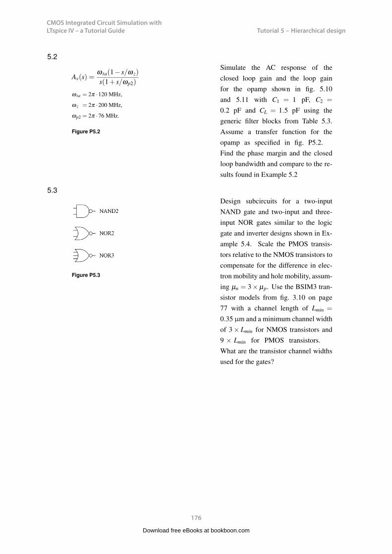
CMOS Integrated Circuit Simulation with LTspice IV – a Tutorial Guide
176
Tutorial 5 – Hierarchical designCMOS Integrated Circuit Simulation with LTspice IV Tutorial 5
5.2
Av(s) =ω ta(1− s/ω z)
s(1+ s/ωp2)
ω ta = 2π ·120 MHz,
ω z = 2π ·200 MHz,
ωp2 = 2π ·76 MHz.
Figure P5.2
Simulate the AC response of theclosed loop gain and the loop gainfor the opamp shown in fig. 5.10and 5.11 with C1 = 1 pF, C2 =
0.2 pF and CL = 1.5 pF using thegeneric filter blocks from Table 5.3.Assume a transfer function for theopamp as specified in fig. P5.2.Find the phase margin and the closedloop bandwidth and compare to the re-sults found in Example 5.2
5.3
Figure P5.3
Design subcircuits for a two-inputNAND gate and two-input and three-input NOR gates similar to the logicgate and inverter designs shown in Ex-ample 5.4. Scale the PMOS transis-tors relative to the NMOS transistors tocompensate for the difference in elec-tron mobility and hole mobility, assum-ing µn = 3× µp. Use the BSIM3 tran-sistor models from fig. 3.10 on page77 with a channel length of Lmin =
0.35 µm and a minimum channel widthof 3× Lmin for NMOS transistors and9 × Lmin for PMOS transistors.What are the transistor channel widthsused for the gates?
176
Download free eBooks at bookboon.com

CMOS Integrated Circuit Simulation with LTspice IV – a Tutorial Guide
177
Tutorial 5 – Hierarchical designCMOS Integrated Circuit Simulation with LTspice IV Tutorial 5
5.4
Figure P5.4
Use the inverter from fig. 5.25 on page170 to design a ring oscillator as shownin fig. P5.4. Use the BSIM3 transistormodels from fig. 3.10 on page 77 witha channel length of Lmin = 0.35 µmand a supply voltage of 3 V. WithFanout=1 and CF = 0.2 pF, findthe frequency of oscillation. Alsofind the inverter delay for an inverterloaded with an identical inverter.Repeat for Fanout=5 for all ofthe inverters.Hint: To start the oscillation, inject ashort current pulse in the output node.
177
Download free eBooks at bookboon.com
Click on the ad to read moreClick on the ad to read moreClick on the ad to read moreClick on the ad to read moreClick on the ad to read moreClick on the ad to read moreClick on the ad to read moreClick on the ad to read moreClick on the ad to read moreClick on the ad to read moreClick on the ad to read moreClick on the ad to read moreClick on the ad to read moreClick on the ad to read moreClick on the ad to read moreClick on the ad to read moreClick on the ad to read moreClick on the ad to read moreClick on the ad to read moreClick on the ad to read moreClick on the ad to read moreClick on the ad to read moreClick on the ad to read moreClick on the ad to read moreClick on the ad to read moreClick on the ad to read moreClick on the ad to read moreClick on the ad to read moreClick on the ad to read moreClick on the ad to read moreClick on the ad to read moreClick on the ad to read moreClick on the ad to read moreClick on the ad to read moreClick on the ad to read moreClick on the ad to read moreClick on the ad to read moreClick on the ad to read moreClick on the ad to read moreClick on the ad to read moreClick on the ad to read moreClick on the ad to read moreClick on the ad to read moreClick on the ad to read moreClick on the ad to read moreClick on the ad to read moreClick on the ad to read moreClick on the ad to read moreClick on the ad to read moreClick on the ad to read moreClick on the ad to read moreClick on the ad to read moreClick on the ad to read moreClick on the ad to read moreClick on the ad to read moreClick on the ad to read moreClick on the ad to read moreClick on the ad to read moreClick on the ad to read moreClick on the ad to read moreClick on the ad to read moreClick on the ad to read more
© Deloitte & Touche LLP and affiliated entities.
360°thinking.
Discover the truth at www.deloitte.ca/careers
© Deloitte & Touche LLP and affiliated entities.
360°thinking.
Discover the truth at www.deloitte.ca/careers
© Deloitte & Touche LLP and affiliated entities.
360°thinking.
Discover the truth at www.deloitte.ca/careers © Deloitte & Touche LLP and affiliated entities.
360°thinking.
Discover the truth at www.deloitte.ca/careers

CMOS Integrated Circuit Simulation with LTspice IV – a Tutorial Guide
178
Tutorial 5 – Hierarchical designCMOS Integrated Circuit Simulation with LTspice IV Tutorial 5
Answers
5.1: VB = 1.505 V; low frequency gain: 24.9 dB; dominant pole, simulated: 12 kHz;dominant pole, calculated: 12 kHz.
5.2: Phase margin: 70; Closed loop bandwidth: 30.7 MHz.
5.3: NOR2: Wn = 3×Lmin, Wp = 18×Lmin; NOR3: Wn = 3×Lmin, Wp = 27×Lmin.NAND2: Wn = 6×Lmin, Wp = 9×Lmin.
5.4: Fanout=1: fosc = 629 MHz, tdelay = 72 ps; Fanout=5: fosc = 1076 MHz, tdelay = 64 ps.
178
Download free eBooks at bookboon.com
CMOS Integrated Circuit Simulation with LTspice IV – a Tutorial Guide
179
Tutorial 6 – Process and parameter variations
CMOS Integrated Circuit Simulation with LTspice IV Tutorial 6
Tutorial 6 – Process and parameter variations
This tutorial illustrates how process variations and parameter variations can be handled with LTspicesimulations. Normally, a design is required to work not only under some typical conditions but alsoover a range of parameter variations such as voltage and temperature variations. Also, tolerance inthe manufacturing processes must be taken into account. This is a major challenge to the designer,involving extensive simulation work during the design process. After having completed the tutorial,you should be able to
– simulate a design in design corners with process, voltage and temperature (PVT) variations.
– design device models for slow, typical and fast process corners.
– evaluate target design parameters using the ‘.measure’ SPICE Directive.
– perform a Monte Carlo simulation.
Often process and parameter variations are treated using a worst-case approach where the worstcombinations of process parameters and operating conditions are simulated in addition to a simu-lation under typical conditions. For the process parameter variations, a standard method is to usedevice models for ‘typical’, ‘fast’ and ‘slow’ devices (Weste & Harris 2010). Thus, for each tran-sistor type (NMOS and PMOS) we have three different models, a typical model, a fast model anda slow model. This leads to the process corners SS, FS, SF and FF where the first letter indicatesthe NMOS model and the second letter indicates the PMOS model (F for fast, S for slow). This isillustrated in fig. 6.1, showing the four process corners for a design target in addition to the typicalset of parameters. Generally, it is assumed that for any combination of parameter variations, thedesign target will fall within the shaded area shown in the figure. Also for resistors and capacitors,typically fast and slow models or values must be considered.
The process parameter variations may be combined with simulations taking operating conditionssuch as supply voltage and temperature into account. This is often termed PVT variations (Carusone,
179
Download free eBooks at bookboon.com
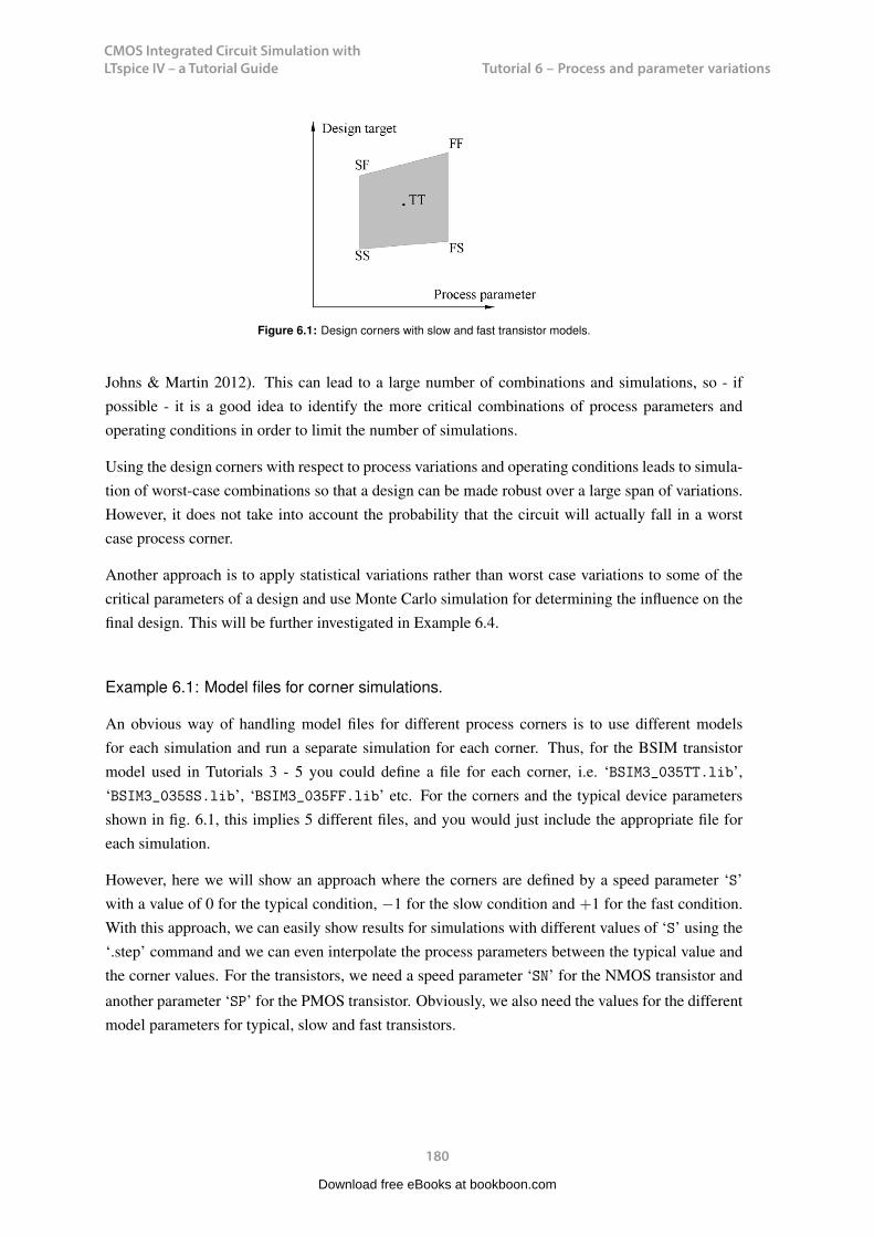
CMOS Integrated Circuit Simulation with LTspice IV – a Tutorial Guide
180
Tutorial 6 – Process and parameter variationsCMOS Integrated Circuit Simulation with LTspice IV Tutorial 6
Figure 6.1: Design corners with slow and fast transistor models.
Johns & Martin 2012). This can lead to a large number of combinations and simulations, so - ifpossible - it is a good idea to identify the more critical combinations of process parameters andoperating conditions in order to limit the number of simulations.
Using the design corners with respect to process variations and operating conditions leads to simula-tion of worst-case combinations so that a design can be made robust over a large span of variations.However, it does not take into account the probability that the circuit will actually fall in a worstcase process corner.
Another approach is to apply statistical variations rather than worst case variations to some of thecritical parameters of a design and use Monte Carlo simulation for determining the influence on thefinal design. This will be further investigated in Example 6.4.
Example 6.1: Model files for corner simulations.
An obvious way of handling model files for different process corners is to use different modelsfor each simulation and run a separate simulation for each corner. Thus, for the BSIM transistormodel used in Tutorials 3 - 5 you could define a file for each corner, i.e. ‘BSIM3_035TT.lib’,‘BSIM3_035SS.lib’, ‘BSIM3_035FF.lib’ etc. For the corners and the typical device parametersshown in fig. 6.1, this implies 5 different files, and you would just include the appropriate file foreach simulation.
However, here we will show an approach where the corners are defined by a speed parameter ‘S’with a value of 0 for the typical condition, −1 for the slow condition and +1 for the fast condition.With this approach, we can easily show results for simulations with different values of ‘S’ using the‘.step’ command and we can even interpolate the process parameters between the typical value andthe corner values. For the transistors, we need a speed parameter ‘SN’ for the NMOS transistor and
180
CMOS Integrated Circuit Simulation with LTspice IV Tutorial 6
another parameter ‘SP’ for the PMOS transistor. Obviously, we also need the values for the differentmodel parameters for typical, slow and fast transistors.
A general method: Assume that a certain parameter x is defined by a typical value xt , a slow valuexs and a fast value x f . We can define:
∆xs = xs − xt (6.1)
∆x f = x f − xt (6.2)
Using a speed parameter S (with S = 0 for the typical parameter, S =−1 for the slow parameter andS = 1 for the fast parameter), we notice that the function (|S|+S)/2 is equal to S for S positive and0 for S negative. Similarly, the function (|S|− S)/2 is equal to |S| = −S for S negative and 0 for Spositive. Using S, we then have a general expression for x:
x = xt +∆x f × (|S|+S)/2+∆xs × (|S|−S)/2
= xt × (1−|S|)+ xs × (|S|−S)/2+ x f × (|S|+S)/2 (6.3)
With this expression, we achieve x = xt for S = 0, x = xs for S = −1 and x = x f for S = 1 and wehave a linear interpolation between typical, fast and slow values for (non-integer) values of |S|< 1.In LTspice, |x| is given by ‘abs(x)’ and also the function ‘uramp(x)’ is available. This function is
181
Download free eBooks at bookboon.com

CMOS Integrated Circuit Simulation with LTspice IV – a Tutorial Guide
181
Tutorial 6 – Process and parameter variations
CMOS Integrated Circuit Simulation with LTspice IV Tutorial 6
another parameter ‘SP’ for the PMOS transistor. Obviously, we also need the values for the differentmodel parameters for typical, slow and fast transistors.
A general method: Assume that a certain parameter x is defined by a typical value xt , a slow valuexs and a fast value x f . We can define:
∆xs = xs − xt (6.1)
∆x f = x f − xt (6.2)
Using a speed parameter S (with S = 0 for the typical parameter, S =−1 for the slow parameter andS = 1 for the fast parameter), we notice that the function (|S|+S)/2 is equal to S for S positive and0 for S negative. Similarly, the function (|S|− S)/2 is equal to |S| = −S for S negative and 0 for Spositive. Using S, we then have a general expression for x:
x = xt +∆x f × (|S|+S)/2+∆xs × (|S|−S)/2
= xt × (1−|S|)+ xs × (|S|−S)/2+ x f × (|S|+S)/2 (6.3)
With this expression, we achieve x = xt for S = 0, x = xs for S = −1 and x = x f for S = 1 and wehave a linear interpolation between typical, fast and slow values for (non-integer) values of |S|< 1.In LTspice, |x| is given by ‘abs(x)’ and also the function ‘uramp(x)’ is available. This function is
181
Download free eBooks at bookboon.com
Click on the ad to read moreClick on the ad to read moreClick on the ad to read moreClick on the ad to read moreClick on the ad to read moreClick on the ad to read moreClick on the ad to read moreClick on the ad to read moreClick on the ad to read moreClick on the ad to read moreClick on the ad to read moreClick on the ad to read moreClick on the ad to read moreClick on the ad to read moreClick on the ad to read moreClick on the ad to read moreClick on the ad to read moreClick on the ad to read moreClick on the ad to read moreClick on the ad to read moreClick on the ad to read moreClick on the ad to read moreClick on the ad to read moreClick on the ad to read moreClick on the ad to read moreClick on the ad to read moreClick on the ad to read moreClick on the ad to read moreClick on the ad to read moreClick on the ad to read moreClick on the ad to read moreClick on the ad to read moreClick on the ad to read moreClick on the ad to read moreClick on the ad to read moreClick on the ad to read moreClick on the ad to read moreClick on the ad to read moreClick on the ad to read moreClick on the ad to read moreClick on the ad to read moreClick on the ad to read moreClick on the ad to read moreClick on the ad to read moreClick on the ad to read moreClick on the ad to read moreClick on the ad to read moreClick on the ad to read moreClick on the ad to read moreClick on the ad to read moreClick on the ad to read moreClick on the ad to read moreClick on the ad to read moreClick on the ad to read moreClick on the ad to read moreClick on the ad to read moreClick on the ad to read moreClick on the ad to read moreClick on the ad to read moreClick on the ad to read moreClick on the ad to read moreClick on the ad to read moreClick on the ad to read more
We will turn your CV into an opportunity of a lifetime
Do you like cars? Would you like to be a part of a successful brand?We will appreciate and reward both your enthusiasm and talent.Send us your CV. You will be surprised where it can take you.
Send us your CV onwww.employerforlife.com
CMOS Integrated Circuit Simulation with LTspice IV – a Tutorial Guide
182
Tutorial 6 – Process and parameter variationsCMOS Integrated Circuit Simulation with LTspice IV Tutorial 6
defined as ‘uramp(x)= (|x|+x)/2’ and using this, (6.3) would appear as
X=Xt*(1-abs(S))+Xs*uramp(-S)+Xf*uramp(S) (6.4)
with the values for Xt, Xs and Xf inserted in the expression.
Specific examples: The approach described above is generally applicable when you have themodel parameters given by specific values for typical, fast and slow conditions. Occasionally, themodel parameters may be specified by a relative variation or an absolute variation instead. For ex-ample, a capacitor may be specified by a nominal value Cnom and a tolerance δ in percent, or athreshold voltage may be specified by a nominal value Vth,nom and a tolerance ∆Vth in absolute value(volts). In such cases the introduction of the speed parameter S is even simpler:
C =Cnom(1−S×δ/100) (6.5)
assuming that a small value of C is the fast model, and
Vth =Vth,nom −S×∆Vth (6.6)
for an NMOS transistor which is faster for smaller values of Vth.
An examination of the BSIM3 models for the 0.35 µm process from (Carusone, Johns & Martin2014) shows that only 5 parameters are different for typical, fast and slow transistor models. Theseare:
The threshold voltage: The threshold voltage parameter VTH0 is given by a nominal value and athreshold voltage shift of ±0.1 V, increasing the numeric value of the threshold voltage forslow transistors and decreasing it for fast transistors.
The oxide thickness: The parameter for gate oxide thickness TOX is given by a nominal value whichis divided by 0.95 for the slow models and by 1.05 for the fast models.
The mobility: The mobility U0 is given by a nominal value which is multiplied by (0.95)2 for theslow models and by (1.05)2 for the fast models.
The bulk junction bottom capacitance: The zero-bias bulk junction bottom capacitance per unitarea CJ is given by a nominal value which is divided by 0.95 for the slow models and by 1.05for the fast models.
The bulk junction sidewall capacitance: The zero-bias bulk junction bottom capacitance per unitperimeter CJSW is given by a nominal value which is divided by 0.95 for the slow models andby 1.05 for the fast models.
182
Download free eBooks at bookboon.com
CMOS Integrated Circuit Simulation with LTspice IV – a Tutorial Guide
183
Tutorial 6 – Process and parameter variationsCMOS Integrated Circuit Simulation with LTspice IV Tutorial 6
Using the speed parameters SN for NMOS transistors and SP for PMOS transistors, these relationscan be modeled as follows (with the nominal values inserted):
NMOS transistors:
VTH0 = 0.48−SN/10 (6.7)
TOX = 7.8E−9/(1+SN/20) (6.8)
U0 = 360∗ (1+SN/20)∗∗2 (6.9)
CJ = 9e−4/(1+SN/20) (6.10)
CJSW = 2.8e−10/(1+SN/20) (6.11)
PMOS transistors:
VTH0 = −0.6+SP/10 (6.12)
TOX = 7.8E−9/(1+SP/20) (6.13)
U0 = 150∗ (1+SP/20)∗∗2 (6.14)
CJ = 14e−4/(1+SP/20) (6.15)
CJSW = 3.2e−10/(1+SP/20) (6.16)
Inserting the expressions (6.7 - 6.16) in the models from fig. 3.10 on page 77, we have the library fileBSIM3_035PVT.lib shown in fig. 6.2. This file can be directly copied into a text editor and saved asBSIM3_035PVT.lib for use with LTspice.
Combining the speed parameters into a single parameter: Sometimes it may be useful to com-bine a set of speed parameters and/or temperature parameters into a single parameter by which youcan step through a desired sequence of combinations of the different parameters, rather than step-ping each parameter individually. It reduces the number of ‘.step’ commands (LTspice can handle amaximum of three levels of nested ‘.step’ commands), and it reduces the total number of simulationsto include only the PVT corners of interest. This can be done by using the ‘.step’ command in com-bination with the command ‘.param <param_name>=table(N,a,b,c,d,...)’. Assume for instance thatwe want to step through the process corners shown in fig. 6.1 in the sequence TT, SS, FS, SF, FF.This corresponds to the sequence (SN,SP)=(0,0), (−1,−1), (1,−1), (−1,1), (1,1). Using a parameter‘N’ as step number to count the steps from 1 to 5, this is accomplished by the following SPICEDirectives:
.step param N 1 5 1
183
Download free eBooks at bookboon.com
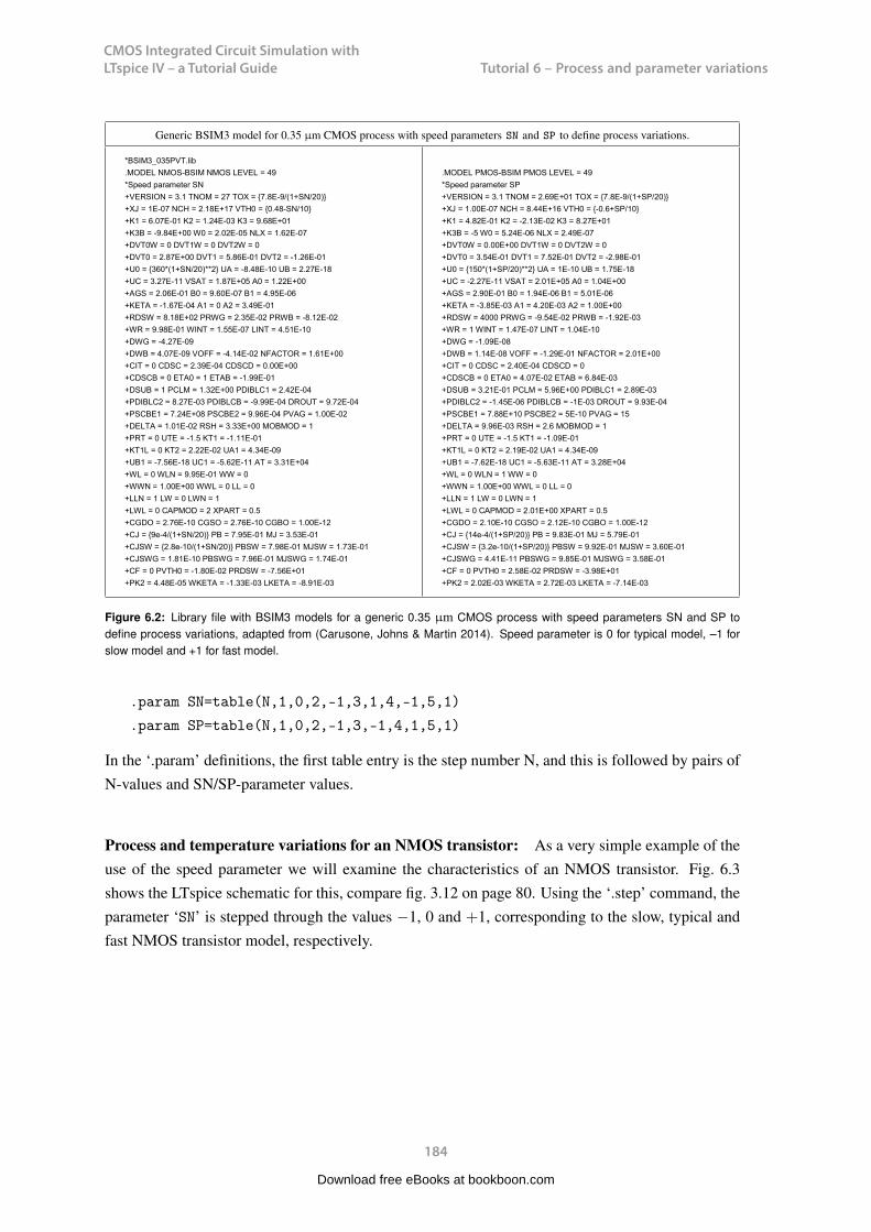
CMOS Integrated Circuit Simulation with LTspice IV – a Tutorial Guide
184
Tutorial 6 – Process and parameter variationsCMOS Integrated Circuit Simulation with LTspice IV Tutorial 6
Generic BSIM3 model for 0.35 µm CMOS process with speed parameters SN and SP to define process variations.
*BSIM3_035PVT.lib.MODEL NMOS-BSIM NMOS LEVEL = 49*Speed parameter SN+VERSION = 3.1 TNOM = 27 TOX = 7.8E-9/(1+SN/20)+XJ = 1E-07 NCH = 2.18E+17 VTH0 = 0.48-SN/10+K1 = 6.07E-01 K2 = 1.24E-03 K3 = 9.68E+01+K3B = -9.84E+00 W0 = 2.02E-05 NLX = 1.62E-07+DVT0W = 0 DVT1W = 0 DVT2W = 0+DVT0 = 2.87E+00 DVT1 = 5.86E-01 DVT2 = -1.26E-01+U0 = 360*(1+SN/20)**2 UA = -8.48E-10 UB = 2.27E-18+UC = 3.27E-11 VSAT = 1.87E+05 A0 = 1.22E+00+AGS = 2.06E-01 B0 = 9.60E-07 B1 = 4.95E-06+KETA = -1.67E-04 A1 = 0 A2 = 3.49E-01+RDSW = 8.18E+02 PRWG = 2.35E-02 PRWB = -8.12E-02+WR = 9.98E-01 WINT = 1.55E-07 LINT = 4.51E-10+DWG = -4.27E-09+DWB = 4.07E-09 VOFF = -4.14E-02 NFACTOR = 1.61E+00+CIT = 0 CDSC = 2.39E-04 CDSCD = 0.00E+00+CDSCB = 0 ETA0 = 1 ETAB = -1.99E-01+DSUB = 1 PCLM = 1.32E+00 PDIBLC1 = 2.42E-04+PDIBLC2 = 8.27E-03 PDIBLCB = -9.99E-04 DROUT = 9.72E-04+PSCBE1 = 7.24E+08 PSCBE2 = 9.96E-04 PVAG = 1.00E-02+DELTA = 1.01E-02 RSH = 3.33E+00 MOBMOD = 1+PRT = 0 UTE = -1.5 KT1 = -1.11E-01+KT1L = 0 KT2 = 2.22E-02 UA1 = 4.34E-09+UB1 = -7.56E-18 UC1 = -5.62E-11 AT = 3.31E+04+WL = 0 WLN = 9.95E-01 WW = 0+WWN = 1.00E+00 WWL = 0 LL = 0+LLN = 1 LW = 0 LWN = 1+LWL = 0 CAPMOD = 2 XPART = 0.5+CGDO = 2.76E-10 CGSO = 2.76E-10 CGBO = 1.00E-12+CJ = 9e-4/(1+SN/20) PB = 7.95E-01 MJ = 3.53E-01+CJSW = 2.8e-10/(1+SN/20) PBSW = 7.98E-01 MJSW = 1.73E-01+CJSWG = 1.81E-10 PBSWG = 7.96E-01 MJSWG = 1.74E-01+CF = 0 PVTH0 = -1.80E-02 PRDSW = -7.56E+01+PK2 = 4.48E-05 WKETA = -1.33E-03 LKETA = -8.91E-03
.MODEL PMOS-BSIM PMOS LEVEL = 49*Speed parameter SP+VERSION = 3.1 TNOM = 2.69E+01 TOX = 7.8E-9/(1+SP/20)+XJ = 1.00E-07 NCH = 8.44E+16 VTH0 = -0.6+SP/10+K1 = 4.82E-01 K2 = -2.13E-02 K3 = 8.27E+01+K3B = -5 W0 = 5.24E-06 NLX = 2.49E-07+DVT0W = 0.00E+00 DVT1W = 0 DVT2W = 0+DVT0 = 3.54E-01 DVT1 = 7.52E-01 DVT2 = -2.98E-01+U0 = 150*(1+SP/20)**2 UA = 1E-10 UB = 1.75E-18+UC = -2.27E-11 VSAT = 2.01E+05 A0 = 1.04E+00+AGS = 2.90E-01 B0 = 1.94E-06 B1 = 5.01E-06+KETA = -3.85E-03 A1 = 4.20E-03 A2 = 1.00E+00+RDSW = 4000 PRWG = -9.54E-02 PRWB = -1.92E-03+WR = 1 WINT = 1.47E-07 LINT = 1.04E-10+DWG = -1.09E-08+DWB = 1.14E-08 VOFF = -1.29E-01 NFACTOR = 2.01E+00+CIT = 0 CDSC = 2.40E-04 CDSCD = 0+CDSCB = 0 ETA0 = 4.07E-02 ETAB = 6.84E-03+DSUB = 3.21E-01 PCLM = 5.96E+00 PDIBLC1 = 2.89E-03+PDIBLC2 = -1.45E-06 PDIBLCB = -1E-03 DROUT = 9.93E-04+PSCBE1 = 7.88E+10 PSCBE2 = 5E-10 PVAG = 15+DELTA = 9.96E-03 RSH = 2.6 MOBMOD = 1+PRT = 0 UTE = -1.5 KT1 = -1.09E-01+KT1L = 0 KT2 = 2.19E-02 UA1 = 4.34E-09+UB1 = -7.62E-18 UC1 = -5.63E-11 AT = 3.28E+04+WL = 0 WLN = 1 WW = 0+WWN = 1.00E+00 WWL = 0 LL = 0+LLN = 1 LW = 0 LWN = 1+LWL = 0 CAPMOD = 2.01E+00 XPART = 0.5+CGDO = 2.10E-10 CGSO = 2.12E-10 CGBO = 1.00E-12+CJ = 14e-4/(1+SP/20) PB = 9.83E-01 MJ = 5.79E-01+CJSW = 3.2e-10/(1+SP/20) PBSW = 9.92E-01 MJSW = 3.60E-01+CJSWG = 4.41E-11 PBSWG = 9.85E-01 MJSWG = 3.58E-01+CF = 0 PVTH0 = 2.58E-02 PRDSW = -3.98E+01+PK2 = 2.02E-03 WKETA = 2.72E-03 LKETA = -7.14E-03
Figure 6.2: Library file with BSIM3 models for a generic 0.35 µm CMOS process with speed parameters SN and SP todefine process variations, adapted from (Carusone, Johns & Martin 2014). Speed parameter is 0 for typical model, –1 forslow model and +1 for fast model.
.param SN=table(N,1,0,2,-1,3,1,4,-1,5,1)
.param SP=table(N,1,0,2,-1,3,-1,4,1,5,1)
In the ‘.param’ definitions, the first table entry is the step number N, and this is followed by pairs ofN-values and SN/SP-parameter values.
Process and temperature variations for an NMOS transistor: As a very simple example of theuse of the speed parameter we will examine the characteristics of an NMOS transistor. Fig. 6.3shows the LTspice schematic for this, compare fig. 3.12 on page 80. Using the ‘.step’ command, theparameter ‘SN’ is stepped through the values −1, 0 and +1, corresponding to the slow, typical andfast NMOS transistor model, respectively.
Fig. 6.4 shows the simulated input characteristics and output characteristics. The input charac-
184
Download free eBooks at bookboon.com

CMOS Integrated Circuit Simulation with LTspice IV – a Tutorial Guide
185
Tutorial 6 – Process and parameter variations
Figure 6.3: LTspice schematic for simulation of transistor characteristics with slow, fast and typical BSIM3 models.
Fig. 6.4 shows the simulated input characteristics and output characteristics. The input charac-teristics are simulated with VDS = 3.0 V so that the transistor is in the active region. The outputcharacteristics are simulated for VGS = 1, 2 and 3 V. It is evident that there is a significant differencein drain current between the fast and slow model, about 50%. For the transistor, often a design targetis a specific value of the transconductance gm, see for instance the design procedure for transistorsM1 and M7 in example 5.2 on page 154 - 165. The transconductance may be simulated as shown infig. 5.12 on page 160. In order to illustrate the variation in gm caused by process variations, we cansimulate the transistor with ID = 100 µA for three different values of the speed parameter ‘SN’, cor-responding to slow, typical and fast parameters. The results of this simulation are shown in fig. 6.5
Download free eBooks at bookboon.com
Click on the ad to read moreClick on the ad to read moreClick on the ad to read moreClick on the ad to read moreClick on the ad to read moreClick on the ad to read moreClick on the ad to read moreClick on the ad to read moreClick on the ad to read moreClick on the ad to read moreClick on the ad to read moreClick on the ad to read moreClick on the ad to read moreClick on the ad to read moreClick on the ad to read moreClick on the ad to read moreClick on the ad to read moreClick on the ad to read moreClick on the ad to read moreClick on the ad to read moreClick on the ad to read moreClick on the ad to read moreClick on the ad to read moreClick on the ad to read moreClick on the ad to read moreClick on the ad to read moreClick on the ad to read moreClick on the ad to read moreClick on the ad to read moreClick on the ad to read moreClick on the ad to read moreClick on the ad to read moreClick on the ad to read moreClick on the ad to read moreClick on the ad to read moreClick on the ad to read moreClick on the ad to read moreClick on the ad to read moreClick on the ad to read moreClick on the ad to read moreClick on the ad to read moreClick on the ad to read moreClick on the ad to read moreClick on the ad to read moreClick on the ad to read moreClick on the ad to read moreClick on the ad to read moreClick on the ad to read moreClick on the ad to read moreClick on the ad to read moreClick on the ad to read moreClick on the ad to read moreClick on the ad to read moreClick on the ad to read moreClick on the ad to read moreClick on the ad to read moreClick on the ad to read moreClick on the ad to read moreClick on the ad to read moreClick on the ad to read moreClick on the ad to read moreClick on the ad to read moreClick on the ad to read moreClick on the ad to read more
Maersk.com/Mitas
e Graduate Programme for Engineers and Geoscientists
Month 16I was a construction
supervisor in the North Sea
advising and helping foremen
solve problems
I was a
hes
Real work International opportunities
ree work placementsal Internationaorree wo
I wanted real responsibili I joined MITAS because
www.discovermitas.com
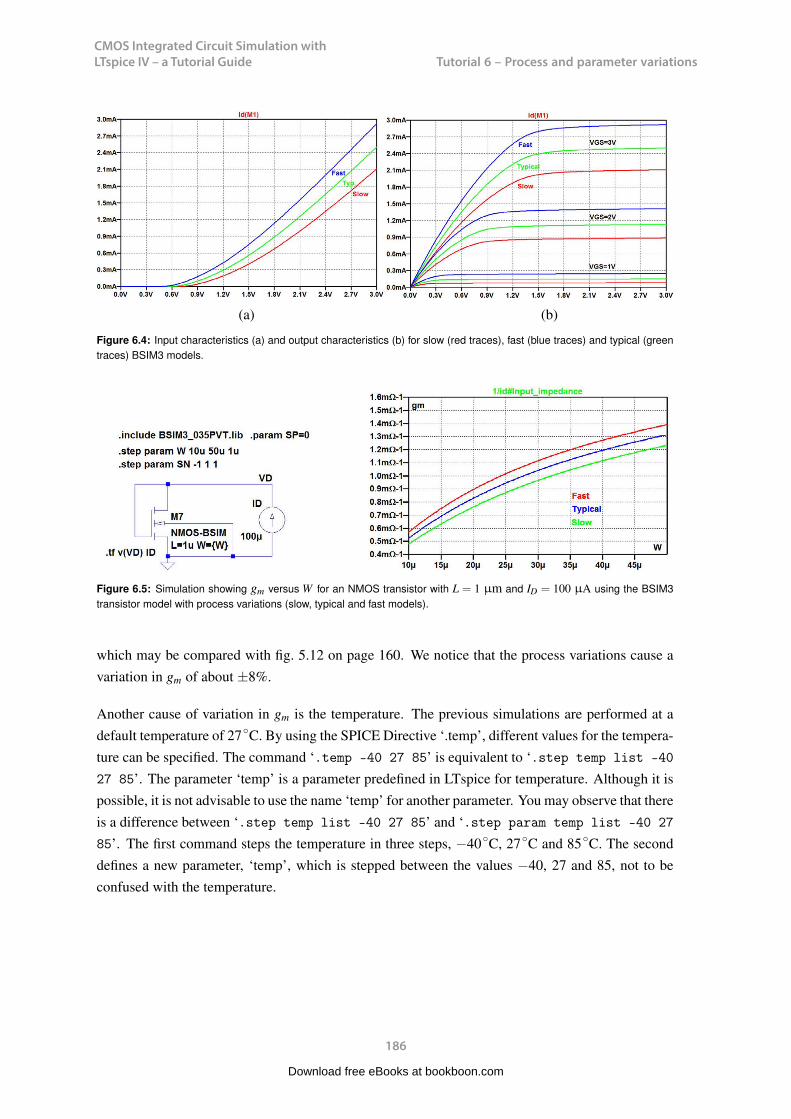
CMOS Integrated Circuit Simulation with LTspice IV – a Tutorial Guide
186
Tutorial 6 – Process and parameter variationsCMOS Integrated Circuit Simulation with LTspice IV Tutorial 6
(a) (b)
Figure 6.4: Input characteristics (a) and output characteristics (b) for slow (red traces), fast (blue traces) and typical (greentraces) BSIM3 models.
Figure 6.5: Simulation showing gm versus W for an NMOS transistor with L = 1 µm and ID = 100 µA using the BSIM3transistor model with process variations (slow, typical and fast models).
which may be compared with fig. 5.12 on page 160. We notice that the process variations cause avariation in gm of about ±8%.
Another cause of variation in gm is the temperature. The previous simulations are performed at adefault temperature of 27C. By using the SPICE Directive ‘.temp’, different values for the tempera-ture can be specified. The command ‘.temp -40 27 85’ is equivalent to ‘.step temp list -40
27 85’. The parameter ‘temp’ is a parameter predefined in LTspice for temperature. Although it ispossible, it is not advisable to use the name ‘temp’ for another parameter. You may observe that thereis a difference between ‘.step temp list -40 27 85’ and ‘.step param temp list -40 27
85’. The first command steps the temperature in three steps, −40C, 27C and 85C. The seconddefines a new parameter, ‘temp’, which is stepped between the values −40, 27 and 85, not to beconfused with the temperature.
186
Download free eBooks at bookboon.com
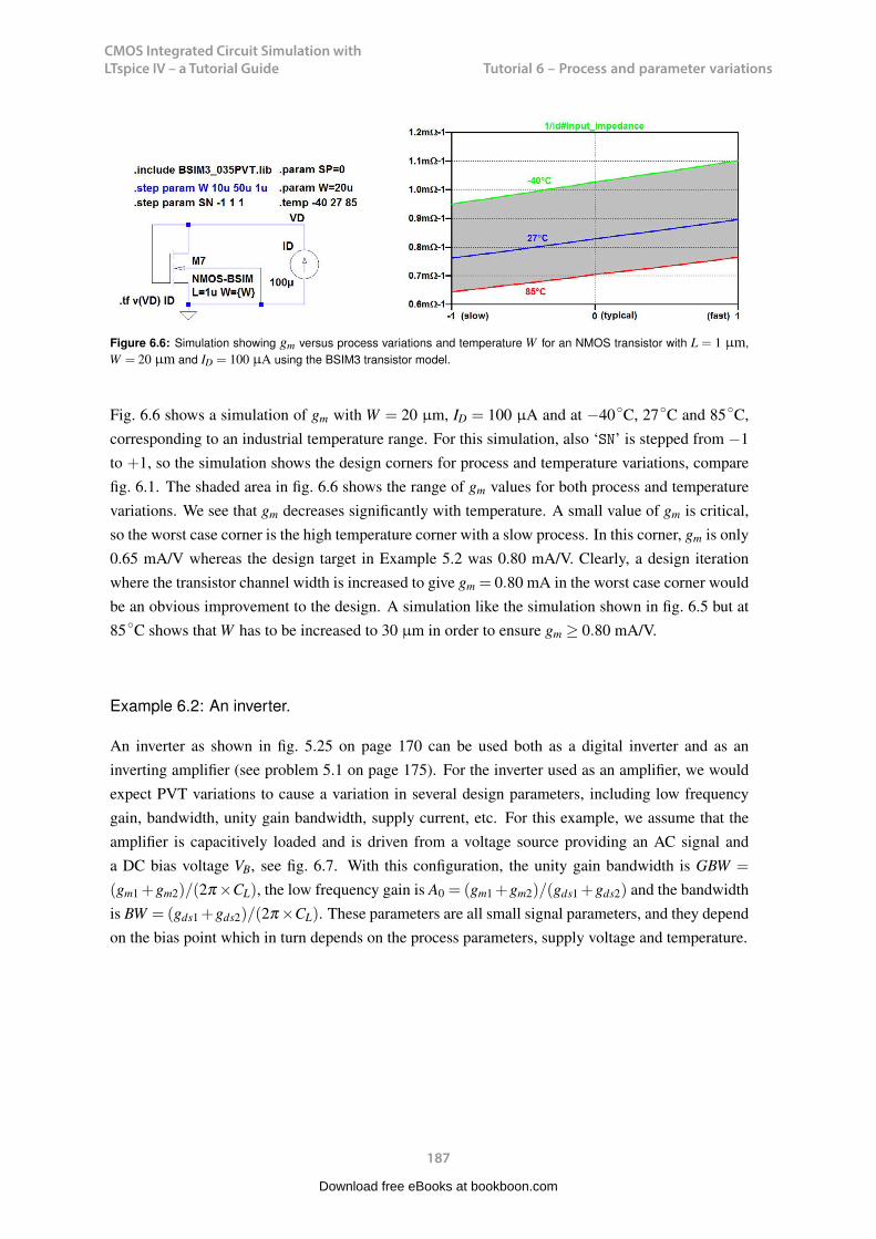
CMOS Integrated Circuit Simulation with LTspice IV – a Tutorial Guide
187
Tutorial 6 – Process and parameter variationsCMOS Integrated Circuit Simulation with LTspice IV Tutorial 6
Figure 6.6: Simulation showing gm versus process variations and temperature W for an NMOS transistor with L = 1 µm,W = 20 µm and ID = 100 µA using the BSIM3 transistor model.
Fig. 6.6 shows a simulation of gm with W = 20 µm, ID = 100 µA and at −40C, 27C and 85C,corresponding to an industrial temperature range. For this simulation, also ‘SN’ is stepped from −1to +1, so the simulation shows the design corners for process and temperature variations, comparefig. 6.1. The shaded area in fig. 6.6 shows the range of gm values for both process and temperaturevariations. We see that gm decreases significantly with temperature. A small value of gm is critical,so the worst case corner is the high temperature corner with a slow process. In this corner, gm is only0.65 mA/V whereas the design target in Example 5.2 was 0.80 mA/V. Clearly, a design iterationwhere the transistor channel width is increased to give gm = 0.80 mA in the worst case corner wouldbe an obvious improvement to the design. A simulation like the simulation shown in fig. 6.5 but at85C shows that W has to be increased to 30 µm in order to ensure gm ≥ 0.80 mA/V.
Example 6.2: An inverter.
An inverter as shown in fig. 5.25 on page 170 can be used both as a digital inverter and as aninverting amplifier (see problem 5.1 on page 175). For the inverter used as an amplifier, we wouldexpect PVT variations to cause a variation in several design parameters, including low frequencygain, bandwidth, unity gain bandwidth, supply current, etc. For this example, we assume that theamplifier is capacitively loaded and is driven from a voltage source providing an AC signal anda DC bias voltage VB, see fig. 6.7. With this configuration, the unity gain bandwidth is GBW =
(gm1+gm2)/(2π ×CL), the low frequency gain is A0 = (gm1+gm2)/(gds1+gds2) and the bandwidthis BW = (gds1+gds2)/(2π ×CL). These parameters are all small signal parameters, and they dependon the bias point which in turn depends on the process parameters, supply voltage and temperature.
187
Download free eBooks at bookboon.com

CMOS Integrated Circuit Simulation with LTspice IV – a Tutorial Guide
188
Tutorial 6 – Process and parameter variationsCMOS Integrated Circuit Simulation with LTspice IV Tutorial 6
Figure 6.7: LTspice schematic of the inverting amplifier showing a selection of ‘.measure’ commands.
DC Sweep: Also large signal properties such as DC transfer characteristics and peak supply cur-rent exhibit PVT variations. As the first investigation, we show the DC transfer characteristics forthe process corners in fig. 6.8. We observe that a fast NMOS transistor pulls the transfer character-istics to the left whereas a fast PMOS transistor pulls the characteristics to the right. Obviously, the
188
CMOS Integrated Circuit Simulation with LTspice IV Tutorial 6
Figure 6.8: DC sweep, output voltage versus input voltage for the inverter from fig. 6.7.
bias value VB of the input voltage for an output quiescent value of about 1.5 V varies between 1.3 Vand 1.7 V.
From the DC sweep we can also find the low frequency gain and the supply current by plotting‘d(V(vout))’ and ‘-I(Vdd)’, respectively, as shown in fig. 6.9.By using the ‘.measure’ (or ‘.meas’) command we can analyze gain and supply current in the processcorners. In fig. 6.7 four different ‘.measure’ commands are shown.
Figure 6.9: DC sweep, low frequency gain versus input voltage (top) and peak current consumption versus input voltage(bottom) for the inverter from fig. 6.7.
189
Download free eBooks at bookboon.com
Click on the ad to read moreClick on the ad to read moreClick on the ad to read moreClick on the ad to read moreClick on the ad to read moreClick on the ad to read moreClick on the ad to read moreClick on the ad to read moreClick on the ad to read moreClick on the ad to read moreClick on the ad to read moreClick on the ad to read moreClick on the ad to read moreClick on the ad to read moreClick on the ad to read moreClick on the ad to read moreClick on the ad to read moreClick on the ad to read moreClick on the ad to read moreClick on the ad to read moreClick on the ad to read moreClick on the ad to read moreClick on the ad to read moreClick on the ad to read moreClick on the ad to read moreClick on the ad to read moreClick on the ad to read moreClick on the ad to read moreClick on the ad to read moreClick on the ad to read moreClick on the ad to read moreClick on the ad to read moreClick on the ad to read moreClick on the ad to read moreClick on the ad to read moreClick on the ad to read moreClick on the ad to read moreClick on the ad to read moreClick on the ad to read moreClick on the ad to read moreClick on the ad to read moreClick on the ad to read moreClick on the ad to read moreClick on the ad to read moreClick on the ad to read moreClick on the ad to read moreClick on the ad to read moreClick on the ad to read moreClick on the ad to read moreClick on the ad to read moreClick on the ad to read moreClick on the ad to read moreClick on the ad to read moreClick on the ad to read moreClick on the ad to read moreClick on the ad to read moreClick on the ad to read moreClick on the ad to read moreClick on the ad to read moreClick on the ad to read moreClick on the ad to read moreClick on the ad to read moreClick on the ad to read moreClick on the ad to read moreClick on the ad to read more
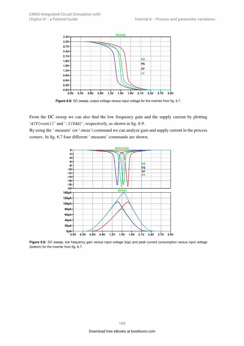
CMOS Integrated Circuit Simulation with LTspice IV – a Tutorial Guide
189
Tutorial 6 – Process and parameter variationsCMOS Integrated Circuit Simulation with LTspice IV Tutorial 6
Figure 6.8: DC sweep, output voltage versus input voltage for the inverter from fig. 6.7.
bias value VB of the input voltage for an output quiescent value of about 1.5 V varies between 1.3 Vand 1.7 V.
From the DC sweep we can also find the low frequency gain and the supply current by plotting‘d(V(vout))’ and ‘-I(Vdd)’, respectively, as shown in fig. 6.9.By using the ‘.measure’ (or ‘.meas’) command we can analyze gain and supply current in the processcorners. In fig. 6.7 four different ‘.measure’ commands are shown.
Figure 6.9: DC sweep, low frequency gain versus input voltage (top) and peak current consumption versus input voltage(bottom) for the inverter from fig. 6.7.
189
CMOS Integrated Circuit Simulation with LTspice IV Tutorial 6
Figure 6.8: DC sweep, output voltage versus input voltage for the inverter from fig. 6.7.
bias value VB of the input voltage for an output quiescent value of about 1.5 V varies between 1.3 Vand 1.7 V.
From the DC sweep we can also find the low frequency gain and the supply current by plotting‘d(V(vout))’ and ‘-I(Vdd)’, respectively, as shown in fig. 6.9.By using the ‘.measure’ (or ‘.meas’) command we can analyze gain and supply current in the processcorners. In fig. 6.7 four different ‘.measure’ commands are shown.
Figure 6.9: DC sweep, low frequency gain versus input voltage (top) and peak current consumption versus input voltage(bottom) for the inverter from fig. 6.7.
189
Download free eBooks at bookboon.com
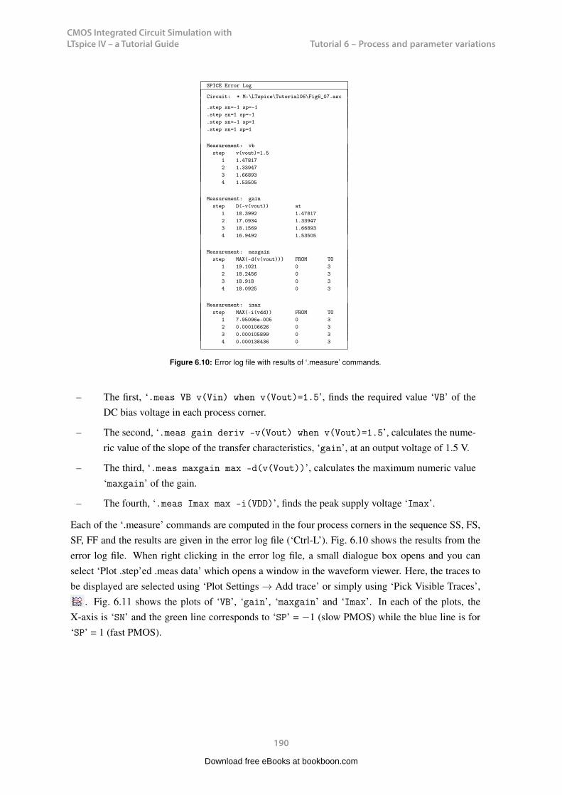
CMOS Integrated Circuit Simulation with LTspice IV – a Tutorial Guide
190
Tutorial 6 – Process and parameter variationsCMOS Integrated Circuit Simulation with LTspice IV Tutorial 6
SPICE Error Log
Circuit: * M:\LTspice\Tutorial06\Fig6_07.asc
.step sn=-1 sp=-1
.step sn=1 sp=-1
.step sn=-1 sp=1
.step sn=1 sp=1
Measurement: vbstep v(vout)=1.5
1 1.478172 1.339473 1.668934 1.53505
Measurement: gainstep D(-v(vout)) at
1 18.3992 1.478172 17.0934 1.339473 18.1569 1.668934 16.9492 1.53505
Measurement: maxgainstep MAX(-d(v(vout))) FROM TO
1 19.1021 0 32 18.2456 0 33 18.918 0 34 18.0925 0 3
Measurement: imaxstep MAX(-i(vdd)) FROM TO
1 7.95096e-005 0 32 0.000106626 0 33 0.000105899 0 34 0.000138436 0 3
Figure 6.10: Error log file with results of ‘.measure’ commands.
– The first, ‘.meas VB v(Vin) when v(Vout)=1.5’, finds the required value ‘VB’ of theDC bias voltage in each process corner.
– The second, ‘.meas gain deriv -v(Vout) when v(Vout)=1.5’, calculates the nume-ric value of the slope of the transfer characteristics, ‘gain’, at an output voltage of 1.5 V.
– The third, ‘.meas maxgain max -d(v(Vout))’, calculates the maximum numeric value‘maxgain’ of the gain.
– The fourth, ‘.meas Imax max -i(VDD)’, finds the peak supply voltage ‘Imax’.
Each of the ‘.measure’ commands are computed in the four process corners in the sequence SS, FS,SF, FF and the results are given in the error log file (‘Ctrl-L’). Fig. 6.10 shows the results from theerror log file. When right clicking in the error log file, a small dialogue box opens and you canselect ‘Plot .step’ed .meas data’ which opens a window in the waveform viewer. Here, the traces tobe displayed are selected using ‘Plot Settings → Add trace’ or simply using ‘Pick Visible Traces’,
. Fig. 6.11 shows the plots of ‘VB’, ‘gain’, ‘maxgain’ and ‘Imax’. In each of the plots, theX-axis is ‘SN’ and the green line corresponds to ‘SP’ = −1 (slow PMOS) while the blue line is for‘SP’ = 1 (fast PMOS).
190
Download free eBooks at bookboon.com

CMOS Integrated Circuit Simulation with LTspice IV – a Tutorial Guide
191
Tutorial 6 – Process and parameter variations
CMOS Integrated Circuit Simulation with LTspice IV Tutorial 6
Figure 6.11: Gain, maximum gain, input bias voltage and peak supply current versus process variations.
191
Download free eBooks at bookboon.com
Click on the ad to read moreClick on the ad to read moreClick on the ad to read moreClick on the ad to read moreClick on the ad to read moreClick on the ad to read moreClick on the ad to read moreClick on the ad to read moreClick on the ad to read moreClick on the ad to read moreClick on the ad to read moreClick on the ad to read moreClick on the ad to read moreClick on the ad to read moreClick on the ad to read moreClick on the ad to read moreClick on the ad to read moreClick on the ad to read moreClick on the ad to read moreClick on the ad to read moreClick on the ad to read moreClick on the ad to read moreClick on the ad to read moreClick on the ad to read moreClick on the ad to read moreClick on the ad to read moreClick on the ad to read moreClick on the ad to read moreClick on the ad to read moreClick on the ad to read moreClick on the ad to read moreClick on the ad to read moreClick on the ad to read moreClick on the ad to read moreClick on the ad to read moreClick on the ad to read moreClick on the ad to read moreClick on the ad to read moreClick on the ad to read moreClick on the ad to read moreClick on the ad to read moreClick on the ad to read moreClick on the ad to read moreClick on the ad to read moreClick on the ad to read moreClick on the ad to read moreClick on the ad to read moreClick on the ad to read moreClick on the ad to read moreClick on the ad to read moreClick on the ad to read moreClick on the ad to read moreClick on the ad to read moreClick on the ad to read moreClick on the ad to read moreClick on the ad to read moreClick on the ad to read moreClick on the ad to read moreClick on the ad to read moreClick on the ad to read moreClick on the ad to read moreClick on the ad to read moreClick on the ad to read moreClick on the ad to read moreClick on the ad to read moreClick on the ad to read more
STUDY AT A TOP RANKED INTERNATIONAL BUSINESS SCHOOL
Reach your full potential at the Stockholm School of Economics, in one of the most innovative cities in the world. The School is ranked by the Financial Times as the number one business school in the Nordic and Baltic countries.
Visit us at www.hhs.se
Swed
en
Stockholm
no.1nine years in a row
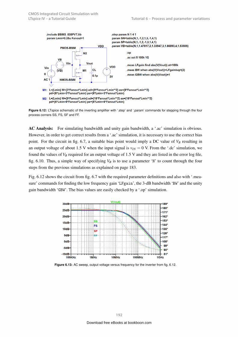
CMOS Integrated Circuit Simulation with LTspice IV – a Tutorial Guide
192
Tutorial 6 – Process and parameter variationsCMOS Integrated Circuit Simulation with LTspice IV Tutorial 6
Figure 6.12: LTspice schematic of the inverting amplifier with ‘.step’ and ‘.param’ commands for stepping through the fourprocess corners SS, FS, SF and FF.
AC Analysis: For simulating bandwidth and unity gain bandwidth, a ‘.ac’ simulation is obvious.However, in order to get correct results from a ‘.ac’ simulation, it is necessary to use the correct biaspoint. For the circuit in fig. 6.7, a suitable bias point would imply a DC value of VB resulting inan output voltage of about 1.5 V when the input signal is vIN = 0 V. From the ‘.dc’ simulation, wefound the values of VB required for an output voltage of 1.5 V and they are listed in the error log file,fig. 6.10. Thus, a simple way of specifying VB is to use a parameter ‘N’ to count through the foursteps from the previous simulations as explained on page 183.
Fig. 6.12 shows the circuit from fig. 6.7 with the required parameter definitions and also with ‘.mea-sure’ commands for finding the low frequency gain ‘LFgain’, the 3-dB bandwidth ‘BW’ and the unitygain bandwidth ‘GBW’. The bias values are easily checked by a ‘.op’ simulation.
Figure 6.13: AC sweep, output voltage versus frequency for the inverter from fig. 6.12.
192
Download free eBooks at bookboon.com

CMOS Integrated Circuit Simulation with LTspice IV – a Tutorial Guide
193
Tutorial 6 – Process and parameter variationsCMOS Integrated Circuit Simulation with LTspice IV Tutorial 6
SPICE Error Log
Circuit: * M:\LTspice\Tutorial06\Fig6_12.asc
.step n=1
.step n=2
.step n=3
.step n=4
Measurement: gbwstep abs(v(vout))=1
1 4.83727e+0082 5.47652e+0083 5.72209e+0084 6.33343e+008
Figure 6.14: Error log file and plot of ‘GBW’ for the inverter from fig. 6.12.
The result of the ‘.ac’ simulation is shown as a Bode plot of ‘V(Vout)’ in fig. 6.13, and fig. 6.14shows the GBW values from the error log file and the graphical plot of GBW (using a right mouseclick in the error log file). With the use of the step number ‘N’ as a parameter rather than separatestep commands for ‘SN’ and ‘SP’, we do not obtain a plot directly showing the process corners ascorners like the plots in fig. 6.11.
Often, a more flexible way of establishing the correct bias conditions for the ‘.ac’ simulation is toprovide a DC feedback from the output to the input. This will automatically adapt the input biasvoltage when process parameters, voltage or temperature are changed. Fig. 6.15 shows two different
193
Download free eBooks at bookboon.com
Click on the ad to read moreClick on the ad to read moreClick on the ad to read moreClick on the ad to read moreClick on the ad to read moreClick on the ad to read moreClick on the ad to read moreClick on the ad to read moreClick on the ad to read moreClick on the ad to read moreClick on the ad to read moreClick on the ad to read moreClick on the ad to read moreClick on the ad to read moreClick on the ad to read moreClick on the ad to read moreClick on the ad to read moreClick on the ad to read moreClick on the ad to read moreClick on the ad to read moreClick on the ad to read moreClick on the ad to read moreClick on the ad to read moreClick on the ad to read moreClick on the ad to read moreClick on the ad to read moreClick on the ad to read moreClick on the ad to read moreClick on the ad to read moreClick on the ad to read moreClick on the ad to read moreClick on the ad to read moreClick on the ad to read moreClick on the ad to read moreClick on the ad to read moreClick on the ad to read moreClick on the ad to read moreClick on the ad to read moreClick on the ad to read moreClick on the ad to read moreClick on the ad to read moreClick on the ad to read moreClick on the ad to read moreClick on the ad to read moreClick on the ad to read moreClick on the ad to read moreClick on the ad to read moreClick on the ad to read moreClick on the ad to read moreClick on the ad to read moreClick on the ad to read moreClick on the ad to read moreClick on the ad to read moreClick on the ad to read moreClick on the ad to read moreClick on the ad to read moreClick on the ad to read moreClick on the ad to read moreClick on the ad to read moreClick on the ad to read moreClick on the ad to read moreClick on the ad to read moreClick on the ad to read moreClick on the ad to read moreClick on the ad to read moreClick on the ad to read moreClick on the ad to read more
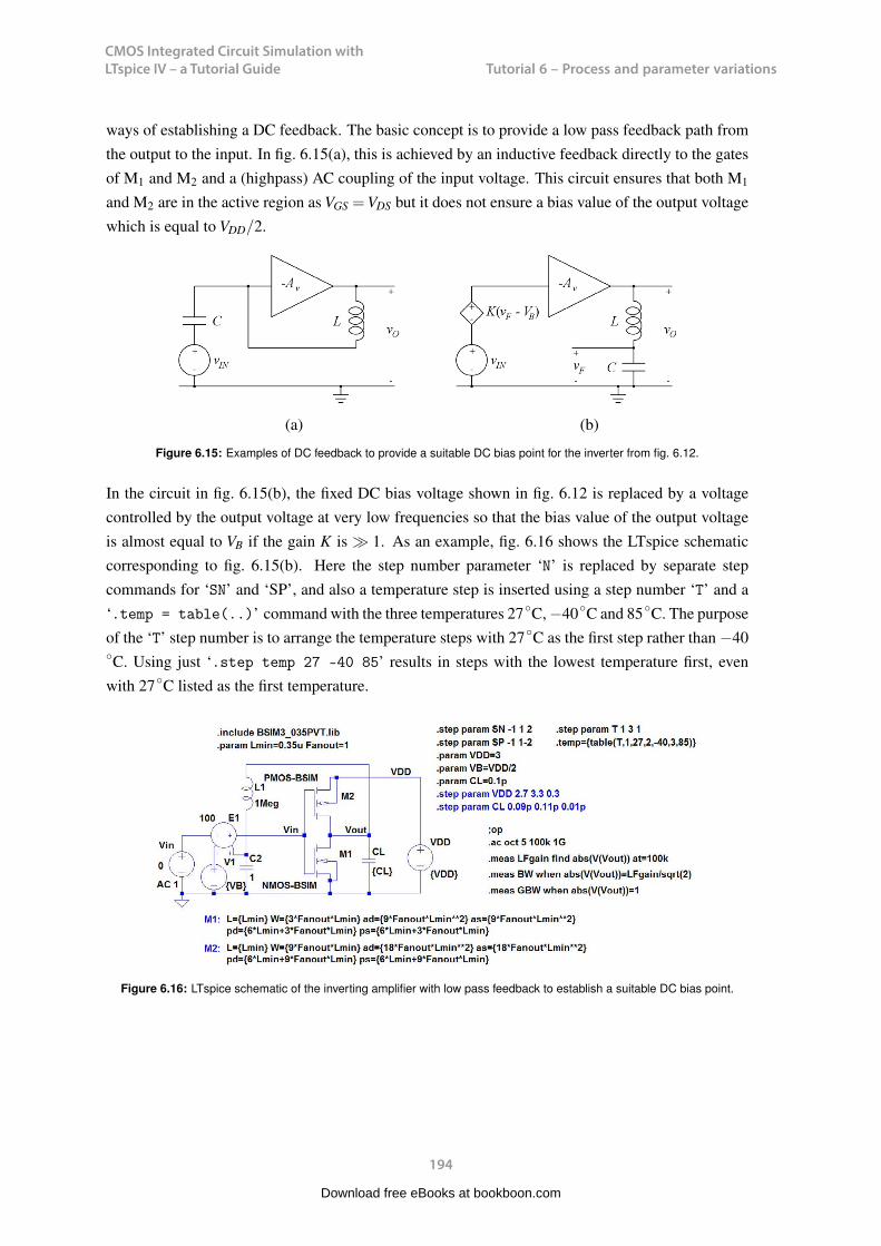
CMOS Integrated Circuit Simulation with LTspice IV – a Tutorial Guide
194
Tutorial 6 – Process and parameter variationsCMOS Integrated Circuit Simulation with LTspice IV Tutorial 6
ways of establishing a DC feedback. The basic concept is to provide a low pass feedback path fromthe output to the input. In fig. 6.15(a), this is achieved by an inductive feedback directly to the gatesof M1 and M2 and a (highpass) AC coupling of the input voltage. This circuit ensures that both M1
and M2 are in the active region as VGS =VDS but it does not ensure a bias value of the output voltagewhich is equal to VDD/2.
(a) (b)
Figure 6.15: Examples of DC feedback to provide a suitable DC bias point for the inverter from fig. 6.12.
In the circuit in fig. 6.15(b), the fixed DC bias voltage shown in fig. 6.12 is replaced by a voltagecontrolled by the output voltage at very low frequencies so that the bias value of the output voltageis almost equal to VB if the gain K is 1. As an example, fig. 6.16 shows the LTspice schematiccorresponding to fig. 6.15(b). Here the step number parameter ‘N’ is replaced by separate stepcommands for ‘SN’ and ‘SP’, and also a temperature step is inserted using a step number ‘T’ and a‘.temp = table(..)’ command with the three temperatures 27C, −40C and 85C. The purposeof the ‘T’ step number is to arrange the temperature steps with 27C as the first step rather than −40C. Using just ‘.step temp 27 -40 85’ results in steps with the lowest temperature first, evenwith 27C listed as the first temperature.
Figure 6.16: LTspice schematic of the inverting amplifier with low pass feedback to establish a suitable DC bias point.
194
Download free eBooks at bookboon.com
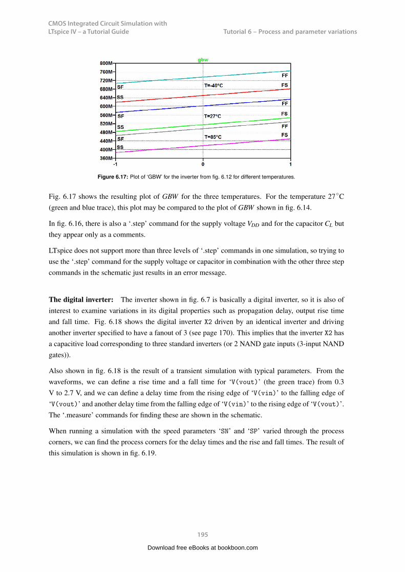
CMOS Integrated Circuit Simulation with LTspice IV – a Tutorial Guide
195
Tutorial 6 – Process and parameter variationsCMOS Integrated Circuit Simulation with LTspice IV Tutorial 6
Figure 6.17: Plot of ‘GBW’ for the inverter from fig. 6.12 for different temperatures.
Fig. 6.17 shows the resulting plot of GBW for the three temperatures. For the temperature 27C(green and blue trace), this plot may be compared to the plot of GBW shown in fig. 6.14.
In fig. 6.16, there is also a ‘.step’ command for the supply voltage VDD and for the capacitor CL butthey appear only as a comments.
LTspice does not support more than three levels of ‘.step’ commands in one simulation, so trying touse the ‘.step’ command for the supply voltage or capacitor in combination with the other three stepcommands in the schematic just results in an error message.
The digital inverter: The inverter shown in fig. 6.7 is basically a digital inverter, so it is also ofinterest to examine variations in its digital properties such as propagation delay, output rise timeand fall time. Fig. 6.18 shows the digital inverter X2 driven by an identical inverter and drivinganother inverter specified to have a fanout of 3 (see page 170). This implies that the inverter X2 hasa capacitive load corresponding to three standard inverters (or 2 NAND gate inputs (3-input NANDgates)).
Also shown in fig. 6.18 is the result of a transient simulation with typical parameters. From thewaveforms, we can define a rise time and a fall time for ‘V(vout)’ (the green trace) from 0.3V to 2.7 V, and we can define a delay time from the rising edge of ‘V(vin)’ to the falling edge of‘V(vout)’ and another delay time from the falling edge of ‘V(vin)’ to the rising edge of ‘V(vout)’.The ‘.measure’ commands for finding these are shown in the schematic.
When running a simulation with the speed parameters ‘SN’ and ‘SP’ varied through the processcorners, we can find the process corners for the delay times and the rise and fall times. The result ofthis simulation is shown in fig. 6.19.
195
Download free eBooks at bookboon.com
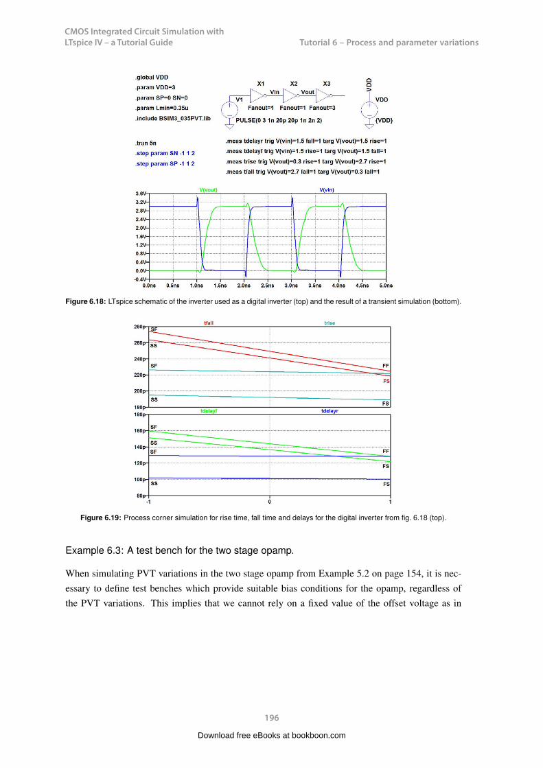
CMOS Integrated Circuit Simulation with LTspice IV – a Tutorial Guide
196
Tutorial 6 – Process and parameter variationsCMOS Integrated Circuit Simulation with LTspice IV Tutorial 6
Figure 6.18: LTspice schematic of the inverter used as a digital inverter (top) and the result of a transient simulation (bottom).
Figure 6.19: Process corner simulation for rise time, fall time and delays for the digital inverter from fig. 6.18 (top).
Example 6.3: A test bench for the two stage opamp.
When simulating PVT variations in the two stage opamp from Example 5.2 on page 154, it is nec-essary to define test benches which provide suitable bias conditions for the opamp, regardless ofthe PVT variations. This implies that we cannot rely on a fixed value of the offset voltage as in
196
Download free eBooks at bookboon.com

CMOS Integrated Circuit Simulation with LTspice IV – a Tutorial Guide
197
Tutorial 6 – Process and parameter variationsCMOS Integrated Circuit Simulation with LTspice IV Tutorial 6
Figure 6.20: Test bench for simulation of loop gain of the two stage opamp with PVT variations.
figs. 5.15 and 5.16 (page 162). Rather, we must ensure a DC feedback path to the inverting opampinput similar to the DC feedback path used for the inverting amplifier in fig. 6.15.
Figs. 6.20 and 6.21 show the test benches from figs. 5.15 and 5.16 modified to include the requiredDC feedback. Also shown are ‘.measure’ commands to find the phase margin and the bandwidth,respectively.
197
Download free eBooks at bookboon.com
Click on the ad to read moreClick on the ad to read moreClick on the ad to read moreClick on the ad to read moreClick on the ad to read moreClick on the ad to read moreClick on the ad to read moreClick on the ad to read moreClick on the ad to read moreClick on the ad to read moreClick on the ad to read moreClick on the ad to read moreClick on the ad to read moreClick on the ad to read moreClick on the ad to read moreClick on the ad to read moreClick on the ad to read moreClick on the ad to read moreClick on the ad to read moreClick on the ad to read moreClick on the ad to read moreClick on the ad to read moreClick on the ad to read moreClick on the ad to read moreClick on the ad to read moreClick on the ad to read moreClick on the ad to read moreClick on the ad to read moreClick on the ad to read moreClick on the ad to read moreClick on the ad to read moreClick on the ad to read moreClick on the ad to read moreClick on the ad to read moreClick on the ad to read moreClick on the ad to read moreClick on the ad to read moreClick on the ad to read moreClick on the ad to read moreClick on the ad to read moreClick on the ad to read moreClick on the ad to read moreClick on the ad to read moreClick on the ad to read moreClick on the ad to read moreClick on the ad to read moreClick on the ad to read moreClick on the ad to read moreClick on the ad to read moreClick on the ad to read moreClick on the ad to read moreClick on the ad to read moreClick on the ad to read moreClick on the ad to read moreClick on the ad to read moreClick on the ad to read moreClick on the ad to read moreClick on the ad to read moreClick on the ad to read moreClick on the ad to read moreClick on the ad to read moreClick on the ad to read moreClick on the ad to read moreClick on the ad to read moreClick on the ad to read moreClick on the ad to read moreClick on the ad to read moreClick on the ad to read more
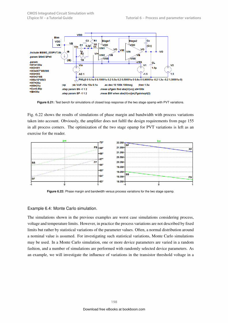
CMOS Integrated Circuit Simulation with LTspice IV – a Tutorial Guide
198
Tutorial 6 – Process and parameter variationsCMOS Integrated Circuit Simulation with LTspice IV Tutorial 6
Figure 6.21: Test bench for simulations of closed loop response of the two stage opamp with PVT variations.
Fig. 6.22 shows the results of simulations of phase margin and bandwidth with process variationstaken into account. Obviously, the amplifier does not fulfil the design requirements from page 155in all process corners. The optimization of the two stage opamp for PVT variations is left as anexercise for the reader.
Figure 6.22: Phase margin and bandwidth versus process variations for the two stage opamp.
Example 6.4: Monte Carlo simulation.
The simulations shown in the previous examples are worst case simulations considering process,voltage and temperature limits. However, in practice the process variations are not described by fixedlimits but rather by statistical variations of the parameter values. Often, a normal distribution arounda nominal value is assumed. For investigating such statistical variations, Monte Carlo simulationsmay be used. In a Monte Carlo simulation, one or more device parameters are varied in a randomfashion, and a number of simulations are performed with randomly selected device parameters. Asan example, we will investigate the influence of variations in the transistor threshold voltage in a
198
Download free eBooks at bookboon.com

CMOS Integrated Circuit Simulation with LTspice IV – a Tutorial Guide
199
Tutorial 6 – Process and parameter variationsCMOS Integrated Circuit Simulation with LTspice IV Tutorial 6
Figure 6.23: Current mirror for Monte Carlo simulation with threshold voltage mismatch.
simple current mirror. For simplicity, we assume a Shichman-Hodges transistor model. Fig. 6.23shows the current mirror with the Shichman-Hodges models for transistor M1 and M2. For transistorM1, the model from fig. 3.3 on page 71 is used, but for M2, a statistical variation is added to thethreshold voltage so that the two transistors no longer match perfectly.
For M2, the threshold voltage is specified as the fixed value plus a statistical variation. LTspice hasdifferent possibilities for specifying a statistical variation:
199
Download free eBooks at bookboon.com
Click on the ad to read moreClick on the ad to read moreClick on the ad to read moreClick on the ad to read moreClick on the ad to read moreClick on the ad to read moreClick on the ad to read moreClick on the ad to read moreClick on the ad to read moreClick on the ad to read moreClick on the ad to read moreClick on the ad to read moreClick on the ad to read moreClick on the ad to read moreClick on the ad to read moreClick on the ad to read moreClick on the ad to read moreClick on the ad to read moreClick on the ad to read moreClick on the ad to read moreClick on the ad to read moreClick on the ad to read moreClick on the ad to read moreClick on the ad to read moreClick on the ad to read moreClick on the ad to read moreClick on the ad to read moreClick on the ad to read moreClick on the ad to read moreClick on the ad to read moreClick on the ad to read moreClick on the ad to read moreClick on the ad to read moreClick on the ad to read moreClick on the ad to read moreClick on the ad to read moreClick on the ad to read moreClick on the ad to read moreClick on the ad to read moreClick on the ad to read moreClick on the ad to read moreClick on the ad to read moreClick on the ad to read moreClick on the ad to read moreClick on the ad to read moreClick on the ad to read moreClick on the ad to read moreClick on the ad to read moreClick on the ad to read moreClick on the ad to read moreClick on the ad to read moreClick on the ad to read moreClick on the ad to read moreClick on the ad to read moreClick on the ad to read moreClick on the ad to read moreClick on the ad to read moreClick on the ad to read moreClick on the ad to read moreClick on the ad to read moreClick on the ad to read moreClick on the ad to read moreClick on the ad to read moreClick on the ad to read moreClick on the ad to read moreClick on the ad to read moreClick on the ad to read moreClick on the ad to read moreClick on the ad to read more
“The perfect start of a successful, international career.”
CLICK HERE to discover why both socially
and academically the University
of Groningen is one of the best
places for a student to be www.rug.nl/feb/education
Excellent Economics and Business programmes at:
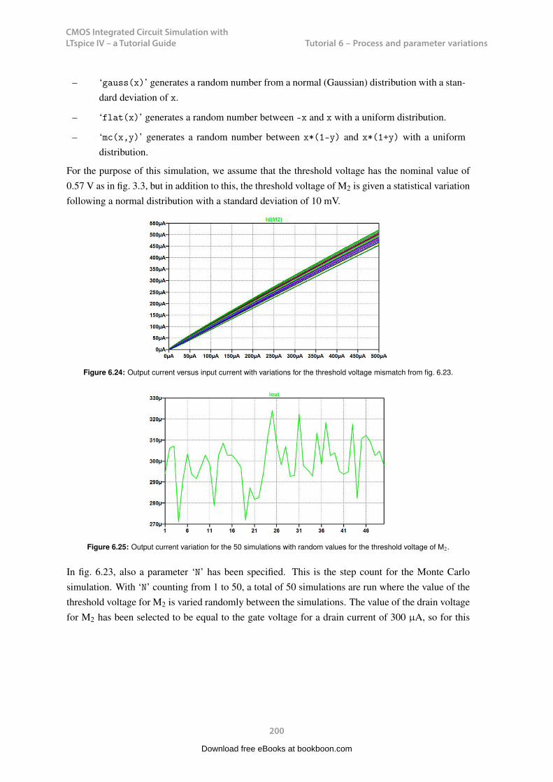
CMOS Integrated Circuit Simulation with LTspice IV – a Tutorial Guide
200
Tutorial 6 – Process and parameter variationsCMOS Integrated Circuit Simulation with LTspice IV Tutorial 6
– ‘gauss(x)’ generates a random number from a normal (Gaussian) distribution with a stan-dard deviation of x.
– ‘flat(x)’ generates a random number between -x and x with a uniform distribution.
– ‘mc(x,y)’ generates a random number between x*(1-y) and x*(1+y) with a uniformdistribution.
For the purpose of this simulation, we assume that the threshold voltage has the nominal value of0.57 V as in fig. 3.3, but in addition to this, the threshold voltage of M2 is given a statistical variationfollowing a normal distribution with a standard deviation of 10 mV.
Figure 6.24: Output current versus input current with variations for the threshold voltage mismatch from fig. 6.23.
Figure 6.25: Output current variation for the 50 simulations with random values for the threshold voltage of M2.
In fig. 6.23, also a parameter ‘N’ has been specified. This is the step count for the Monte Carlosimulation. With ‘N’ counting from 1 to 50, a total of 50 simulations are run where the value of thethreshold voltage for M2 is varied randomly between the simulations. The value of the drain voltagefor M2 has been selected to be equal to the gate voltage for a drain current of 300 µA, so for this
200
Download free eBooks at bookboon.com
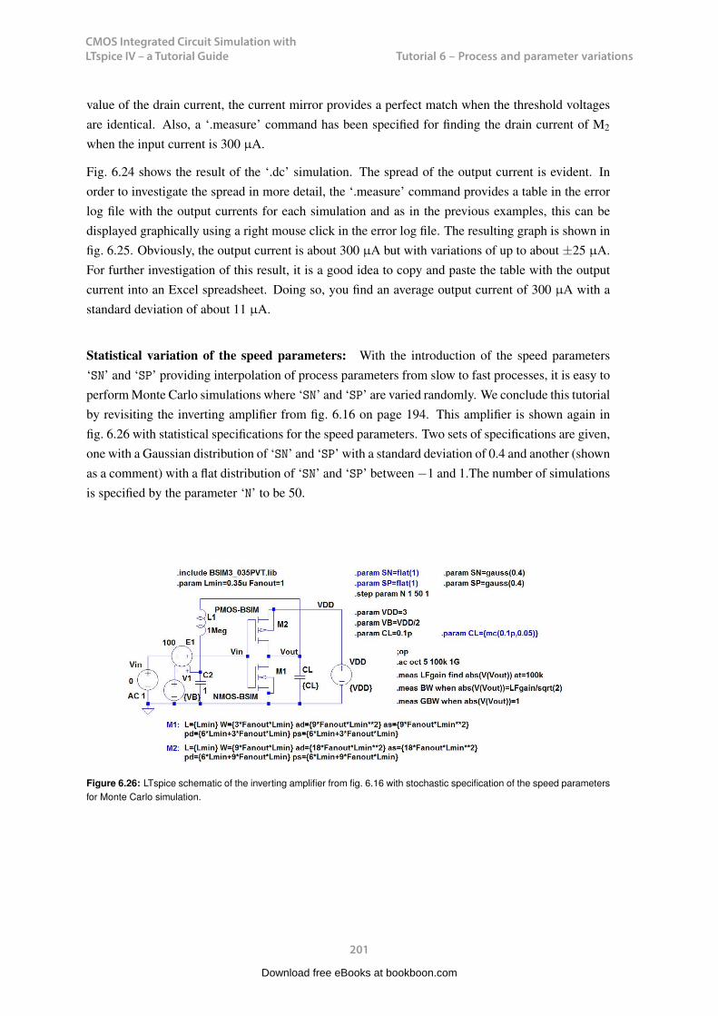
CMOS Integrated Circuit Simulation with LTspice IV – a Tutorial Guide
201
Tutorial 6 – Process and parameter variations
value of the drain current, the current mirror provides a perfect match when the threshold voltagesare identical. Also, a ‘.measure’ command has been specified for finding the drain current of M2
when the input current is 300 µA.
Fig. 6.24 shows the result of the ‘.dc’ simulation. The spread of the output current is evident. Inorder to investigate the spread in more detail, the ‘.measure’ command provides a table in the errorlog file with the output currents for each simulation and as in the previous examples, this can bedisplayed graphically using a right mouse click in the error log file. The resulting graph is shown infig. 6.25. Obviously, the output current is about 300 µA but with variations of up to about ±25 µA.For further investigation of this result, it is a good idea to copy and paste the table with the outputcurrent into an Excel spreadsheet. Doing so, you find an average output current of 300 µA with astandard deviation of about 11 µA.
Statistical variation of the speed parameters: With the introduction of the speed parameters‘SN’ and ‘SP’ providing interpolation of process parameters from slow to fast processes, it is easy toperform Monte Carlo simulations where ‘SN’ and ‘SP’ are varied randomly. We conclude this tutorialby revisiting the inverting amplifier from fig. 6.16 on page 194. This amplifier is shown again infig. 6.26 with statistical specifications for the speed parameters. Two sets of specifications are given,one with a Gaussian distribution of ‘SN’ and ‘SP’ with a standard deviation of 0.4 and another (shownas a comment) with a flat distribution of ‘SN’ and ‘SP’ between −1 and 1.The number of simulationsis specified by the parameter ‘N’ to be 50.
Figure 6.26: LTspice schematic of the inverting amplifier from fig. 6.16 with stochastic specification of the speed parametersfor Monte Carlo simulation.
Download free eBooks at bookboon.com

CMOS Integrated Circuit Simulation with LTspice IV – a Tutorial Guide
202
Tutorial 6 – Process and parameter variations
Figure 6.27: Monte Carlo simulation of the unity gain bandwidth of the inverting amplifier from fig. 6.26.
Fig. 6.27 shows the unity gain bandwidth both for the simulations with a flat distribution and witha Gaussian distribution. This figure may be compared to fig. 6.14 with the results of the worst casecorner simulations. Obviously, assuming the Gaussian distribution, the SS corner and the FF cornerare rather unlikely worst case situations.
Also shown in fig. 6.26 (as a comment) is a stochastic specification of the capacitor CL, specifying atolerance of ±5%. An advantage of the Monte Carlo simulation is that varying values are specifiedwithout using ‘.step’ commands but with stochastic variables instead. Thus, the limitation of threenested ‘.step’ commands is relaxed.
Download free eBooks at bookboon.com
Click on the ad to read moreClick on the ad to read moreClick on the ad to read moreClick on the ad to read moreClick on the ad to read moreClick on the ad to read moreClick on the ad to read moreClick on the ad to read moreClick on the ad to read moreClick on the ad to read moreClick on the ad to read moreClick on the ad to read moreClick on the ad to read moreClick on the ad to read moreClick on the ad to read moreClick on the ad to read moreClick on the ad to read moreClick on the ad to read moreClick on the ad to read moreClick on the ad to read moreClick on the ad to read moreClick on the ad to read moreClick on the ad to read moreClick on the ad to read moreClick on the ad to read moreClick on the ad to read moreClick on the ad to read moreClick on the ad to read moreClick on the ad to read moreClick on the ad to read moreClick on the ad to read moreClick on the ad to read moreClick on the ad to read moreClick on the ad to read moreClick on the ad to read moreClick on the ad to read moreClick on the ad to read moreClick on the ad to read moreClick on the ad to read moreClick on the ad to read moreClick on the ad to read moreClick on the ad to read moreClick on the ad to read moreClick on the ad to read moreClick on the ad to read moreClick on the ad to read moreClick on the ad to read moreClick on the ad to read moreClick on the ad to read moreClick on the ad to read moreClick on the ad to read moreClick on the ad to read moreClick on the ad to read moreClick on the ad to read moreClick on the ad to read moreClick on the ad to read moreClick on the ad to read moreClick on the ad to read moreClick on the ad to read moreClick on the ad to read moreClick on the ad to read moreClick on the ad to read moreClick on the ad to read moreClick on the ad to read moreClick on the ad to read moreClick on the ad to read moreClick on the ad to read moreClick on the ad to read moreClick on the ad to read moreClick on the ad to read more
89,000 kmIn the past four years we have drilled
That’s more than twice around the world.
careers.slb.com
What will you be?
1 Based on Fortune 500 ranking 2011. Copyright © 2015 Schlumberger. All rights reserved.
Who are we?We are the world’s largest oilfield services company1. Working globally—often in remote and challenging locations— we invent, design, engineer, and apply technology to help our customers find and produce oil and gas safely.
Who are we looking for?Every year, we need thousands of graduates to begin dynamic careers in the following domains:n Engineering, Research and Operationsn Geoscience and Petrotechnicaln Commercial and Business
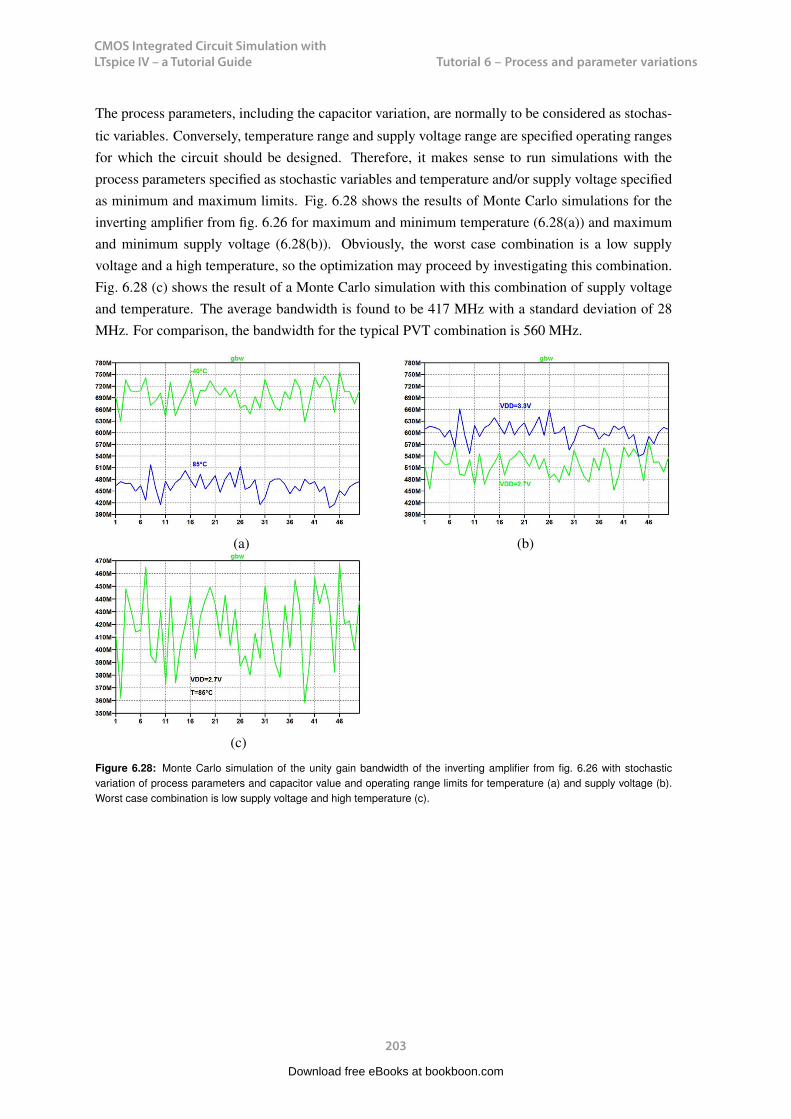
CMOS Integrated Circuit Simulation with LTspice IV – a Tutorial Guide
203
Tutorial 6 – Process and parameter variationsCMOS Integrated Circuit Simulation with LTspice IV Tutorial 6
tic variables. Conversely, temperature range and supply voltage range are specified operating rangesfor which the circuit should be designed. Therefore, it makes sense to run simulations with theprocess parameters specified as stochastic variables and temperature and/or supply voltage specifiedas minimum and maximum limits. Fig. 6.28 shows the results of Monte Carlo simulations for theinverting amplifier from fig. 6.26 for maximum and minimum temperature (6.28(a)) and maximumand minimum supply voltage (6.28(b)). Obviously, the worst case combination is a low supplyvoltage and a high temperature, so the optimization may proceed by investigating this combination.Fig. 6.28 (c) shows the result of a Monte Carlo simulation with this combination of supply voltageand temperature. The average bandwidth is found to be 417 MHz with a standard deviation of 28MHz. For comparison, the bandwidth for the typical PVT combination is 560 MHz.
(a) (b)
(c)
Figure 6.28: Monte Carlo simulation of the unity gain bandwidth of the inverting amplifier from fig. 6.26 with stochasticvariation of process parameters and capacitor value and operating range limits for temperature (a) and supply voltage (b).Worst case combination is low supply voltage and high temperature (c).
203
CMOS Integrated Circuit Simulation with LTspice IV Tutorial 6
Figure 6.27: Monte Carlo simulation of the unity gain bandwidth of the inverting amplifier from fig. 6.26.
a Gaussian distribution. This figure may be compared to fig. 6.14 with the results of the worst casecorner simulations. Obviously, assuming the Gaussian distribution, the SS corner and the FF cornerare rather unlikely worst case situations.
Also shown in fig. 6.26 (as a comment) is a stochastic specification of the capacitor CL, specifying atolerance of ±5%. An advantage of the Monte Carlo simulation is that varying values are specifiedwithout using ‘.step’ commands but with stochastic variables instead. Thus, the limitation of threenested ‘.step’ commands is relaxed.
The process parameters, including the capacitor variation, are normally to be considered as stochas-
202
Download free eBooks at bookboon.com

CMOS Integrated Circuit Simulation with LTspice IV – a Tutorial Guide
204
Tutorial 6 – Process and parameter variationsCMOS Integrated Circuit Simulation with LTspice IV Tutorial 6
Hints and pitfalls
– Process variations may be described by model files for slow, typical and fast compo-nents, leading to different process corners, temperature corners and voltage corners (PVTcorners).
– In order to step between slow, typical and fast components in a single simulation, ‘speed’parameters may be applied to distinguish the different process parameters.
– Stepping between different PVT corners can be achieved by stepping the relevant speedparameters.
– Stepping between selected PVT corners can be customized using a ‘step count’ parameterand a table specification of the selected corners, see example on page 192.
– Temperature is predefined as a parameter ‘temp’ in LTspice. Do not use this name foranother parameter.
– LTspice supports up to three levels of nested ‘.step’ commands.
– ‘.step’ commands are executed in the sequence in which they appear in the SPICE Netlist.This corresponds to the sequence in which they are inserted in the schematic.
– ‘.measure’ commands are very useful for calculating design parameters from simulations.
– The results of ‘.measure’ commands are found in the error log file (‘Ctrl-L’).
– When using ‘.measure’ commands in combination with ‘.step’ commands, the resultingtables in the error log file can be presented in the waveform viewer by using a right mouseclick and selecting ‘Plot .step’ed .meas data’.
– A Monte Carlo simulation is useful for simulating stochastic variations. With a MonteCarlo simulation, several design parameters can simultaneously be subject to variations ina single simulation run.
– Monte Carlo simulations require a fairly large number of simulations, implying that theymight be slow or require a fast computer.
204
Download free eBooks at bookboon.com

CMOS Integrated Circuit Simulation with LTspice IV – a Tutorial Guide
205
Tutorial 6 – Process and parameter variationsCMOS Integrated Circuit Simulation with LTspice IV Tutorial 6
References
Carusone, TC., Johns, D. & Martin, K. 2012, Analog Integrated Circuit Design, Second Edition,John Wiley & Sons, Inc., Hoboken, USA.
Carusone, TC., Johns, D. & Martin, K. 2014, Analog Integrated Circuit Design, Netlist and modelfiles. Retrieved from http://analogicdesign.com/students/netlists-models/
Weste, NHE. & Harris, DM. 2010, CMOS VLSI Design, A Circuits and Systems Perspective, FourthEdition, Addison-Wesley, Boston, USA.
205
Download free eBooks at bookboon.com
Click on the ad to read moreClick on the ad to read moreClick on the ad to read moreClick on the ad to read moreClick on the ad to read moreClick on the ad to read moreClick on the ad to read moreClick on the ad to read moreClick on the ad to read moreClick on the ad to read moreClick on the ad to read moreClick on the ad to read moreClick on the ad to read moreClick on the ad to read moreClick on the ad to read moreClick on the ad to read moreClick on the ad to read moreClick on the ad to read moreClick on the ad to read moreClick on the ad to read moreClick on the ad to read moreClick on the ad to read moreClick on the ad to read moreClick on the ad to read moreClick on the ad to read moreClick on the ad to read moreClick on the ad to read moreClick on the ad to read moreClick on the ad to read moreClick on the ad to read moreClick on the ad to read moreClick on the ad to read moreClick on the ad to read moreClick on the ad to read moreClick on the ad to read moreClick on the ad to read moreClick on the ad to read moreClick on the ad to read moreClick on the ad to read moreClick on the ad to read moreClick on the ad to read moreClick on the ad to read moreClick on the ad to read moreClick on the ad to read moreClick on the ad to read moreClick on the ad to read moreClick on the ad to read moreClick on the ad to read moreClick on the ad to read moreClick on the ad to read moreClick on the ad to read moreClick on the ad to read moreClick on the ad to read moreClick on the ad to read moreClick on the ad to read moreClick on the ad to read moreClick on the ad to read moreClick on the ad to read moreClick on the ad to read moreClick on the ad to read moreClick on the ad to read moreClick on the ad to read moreClick on the ad to read moreClick on the ad to read moreClick on the ad to read moreClick on the ad to read moreClick on the ad to read moreClick on the ad to read moreClick on the ad to read moreClick on the ad to read moreClick on the ad to read more
American online LIGS University
enroll by September 30th, 2014 and
save up to 16% on the tuition!
pay in 10 installments / 2 years
Interactive Online education visit www.ligsuniversity.com to
find out more!
is currently enrolling in theInteractive Online BBA, MBA, MSc,
DBA and PhD programs:
Note: LIGS University is not accredited by any nationally recognized accrediting agency listed by the US Secretary of Education. More info here.
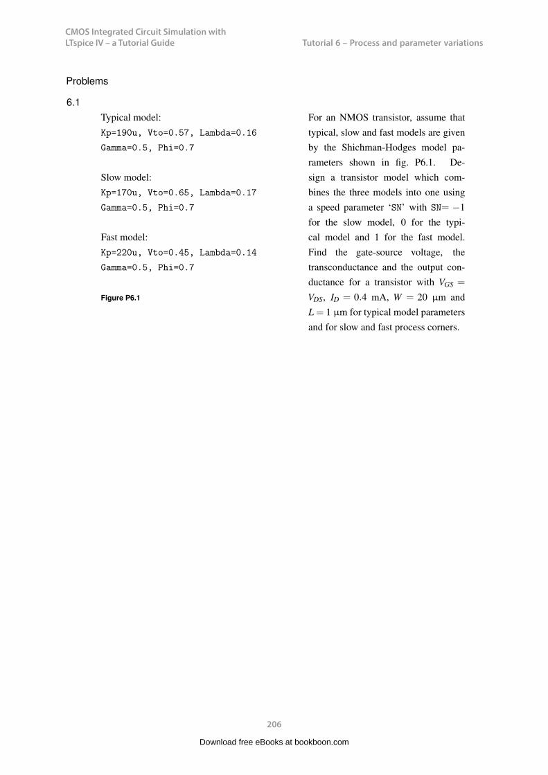
CMOS Integrated Circuit Simulation with LTspice IV – a Tutorial Guide
206
Tutorial 6 – Process and parameter variationsCMOS Integrated Circuit Simulation with LTspice IV Tutorial 6
Problems
6.1Typical model:Kp=190u, Vto=0.57, Lambda=0.16
Gamma=0.5, Phi=0.7
Slow model:Kp=170u, Vto=0.65, Lambda=0.17
Gamma=0.5, Phi=0.7
Fast model:Kp=220u, Vto=0.45, Lambda=0.14
Gamma=0.5, Phi=0.7
Figure P6.1
For an NMOS transistor, assume thattypical, slow and fast models are givenby the Shichman-Hodges model pa-rameters shown in fig. P6.1. De-sign a transistor model which com-bines the three models into one usinga speed parameter ‘SN’ with SN= −1for the slow model, 0 for the typi-cal model and 1 for the fast model.Find the gate-source voltage, thetransconductance and the output con-ductance for a transistor with VGS =
VDS, ID = 0.4 mA, W = 20 µm andL = 1 µm for typical model parametersand for slow and fast process corners.
206
Download free eBooks at bookboon.com

CMOS Integrated Circuit Simulation with LTspice IV – a Tutorial Guide
207
Tutorial 6 – Process and parameter variationsCMOS Integrated Circuit Simulation with LTspice IV Tutorial 6
6.2Design a PMOS transistor to provide agm of at least 0.48 mA/V with VGS =
VDS and ID = 30 µA using a worst casecombination of temperature and pro-cess variations. Assume the BSIM3model shown in fig. 6.2 on page 184and a temperature range from −40Cto 85C. Use a channel length of L = 1µm.
207
Download free eBooks at bookboon.com
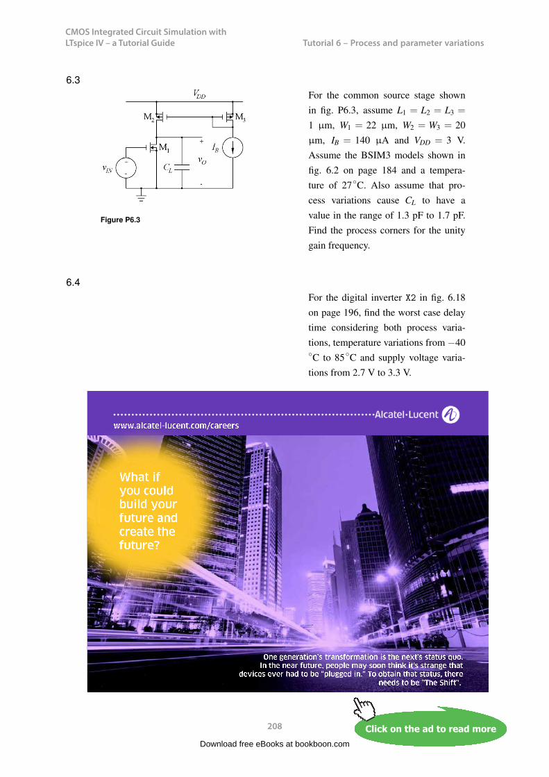
CMOS Integrated Circuit Simulation with LTspice IV – a Tutorial Guide
208
Tutorial 6 – Process and parameter variationsCMOS Integrated Circuit Simulation with LTspice IV Tutorial 6
6.3
Figure P6.3
For the common source stage shownin fig. P6.3, assume L1 = L2 = L3 =
1 µm, W1 = 22 µm, W2 = W3 = 20µm, IB = 140 µA and VDD = 3 V.Assume the BSIM3 models shown infig. 6.2 on page 184 and a tempera-ture of 27C. Also assume that pro-cess variations cause CL to have avalue in the range of 1.3 pF to 1.7 pF.Find the process corners for the unitygain frequency.
6.4For the digital inverter X2 in fig. 6.18on page 196, find the worst case delaytime considering both process varia-tions, temperature variations from −40C to 85C and supply voltage varia-tions from 2.7 V to 3.3 V.
208
Download free eBooks at bookboon.com
Click on the ad to read moreClick on the ad to read moreClick on the ad to read moreClick on the ad to read moreClick on the ad to read moreClick on the ad to read moreClick on the ad to read moreClick on the ad to read moreClick on the ad to read moreClick on the ad to read moreClick on the ad to read moreClick on the ad to read moreClick on the ad to read moreClick on the ad to read moreClick on the ad to read moreClick on the ad to read moreClick on the ad to read moreClick on the ad to read moreClick on the ad to read moreClick on the ad to read moreClick on the ad to read moreClick on the ad to read moreClick on the ad to read moreClick on the ad to read moreClick on the ad to read moreClick on the ad to read moreClick on the ad to read moreClick on the ad to read moreClick on the ad to read moreClick on the ad to read moreClick on the ad to read moreClick on the ad to read moreClick on the ad to read moreClick on the ad to read moreClick on the ad to read moreClick on the ad to read moreClick on the ad to read moreClick on the ad to read moreClick on the ad to read moreClick on the ad to read moreClick on the ad to read moreClick on the ad to read moreClick on the ad to read moreClick on the ad to read moreClick on the ad to read moreClick on the ad to read moreClick on the ad to read moreClick on the ad to read moreClick on the ad to read moreClick on the ad to read moreClick on the ad to read moreClick on the ad to read moreClick on the ad to read moreClick on the ad to read moreClick on the ad to read moreClick on the ad to read moreClick on the ad to read moreClick on the ad to read moreClick on the ad to read moreClick on the ad to read moreClick on the ad to read moreClick on the ad to read moreClick on the ad to read moreClick on the ad to read moreClick on the ad to read moreClick on the ad to read moreClick on the ad to read moreClick on the ad to read moreClick on the ad to read moreClick on the ad to read moreClick on the ad to read moreClick on the ad to read more
.
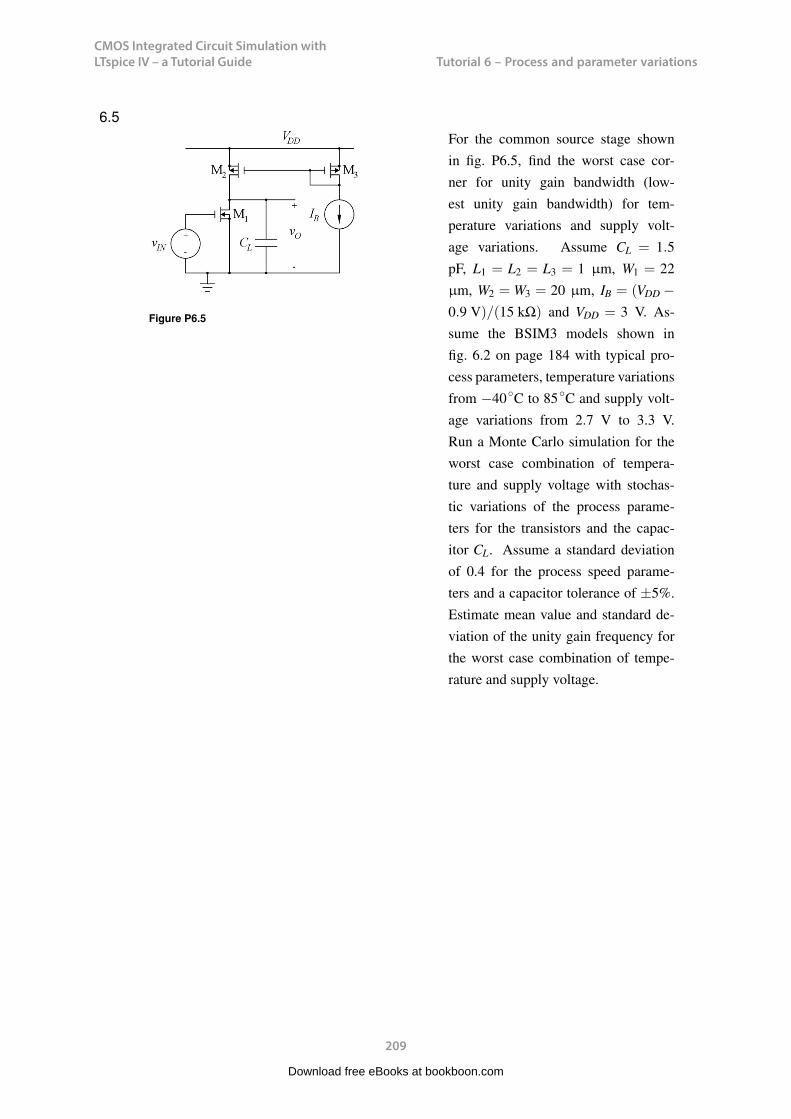
CMOS Integrated Circuit Simulation with LTspice IV – a Tutorial Guide
209
Tutorial 6 – Process and parameter variationsCMOS Integrated Circuit Simulation with LTspice IV Tutorial 6
6.5
Figure P6.5
For the common source stage shownin fig. P6.5, find the worst case cor-ner for unity gain bandwidth (low-est unity gain bandwidth) for tem-perature variations and supply volt-age variations. Assume CL = 1.5pF, L1 = L2 = L3 = 1 µm, W1 = 22µm, W2 = W3 = 20 µm, IB = (VDD −0.9 V)/(15 kΩ) and VDD = 3 V. As-sume the BSIM3 models shown infig. 6.2 on page 184 with typical pro-cess parameters, temperature variationsfrom −40C to 85C and supply volt-age variations from 2.7 V to 3.3 V.Run a Monte Carlo simulation for theworst case combination of tempera-ture and supply voltage with stochas-tic variations of the process parame-ters for the transistors and the capac-itor CL. Assume a standard deviationof 0.4 for the process speed parame-ters and a capacitor tolerance of ±5%.Estimate mean value and standard de-viation of the unity gain frequency forthe worst case combination of tempe-rature and supply voltage.
209
Download free eBooks at bookboon.com

CMOS Integrated Circuit Simulation with LTspice IV – a Tutorial Guide
210
Tutorial 6 – Process and parameter variationsCMOS Integrated Circuit Simulation with LTspice IV Tutorial 6
Answers
6.1: Typical: VGS = 0.996 V; gm = 1.88 mA/V; gds = 55.2 µA/V.Slow: VGS = 1.10 V; gm = 1.80 mA/V; gds = 57.3 µA/V.Fast: VGS = 0.853 V; gm = 1.99 mA/V; gds = 50.0 µA/V.
6.2: Worst case corner: slow process, high temperature. W = 280 µm.
6.3: Process corners: (SN, SP, CL) = (−1, −1, 1.7 pF): GBW = 85.5 MHz.(SN, SP, CL) = (1, −1, 1.7 pF): GBW = 100.8 MHz.(SN, SP, CL) = (−1, 1, 1.3 pF): GBW = 112.3 MHz.(SN, SP, CL) = (1, 1, 1.3 pF): GBW = 133.2 MHz.
6.4: Worst case: falling output, low supply voltage, high temperature, slow processes: tdelay = 191 ps.
6.5: Mean value of GBW : 85.6 MHz. Standard deviation: 3.6 MHz.
210
Download free eBooks at bookboon.com
Click on the ad to read moreClick on the ad to read moreClick on the ad to read moreClick on the ad to read moreClick on the ad to read moreClick on the ad to read moreClick on the ad to read moreClick on the ad to read moreClick on the ad to read moreClick on the ad to read moreClick on the ad to read moreClick on the ad to read moreClick on the ad to read moreClick on the ad to read moreClick on the ad to read moreClick on the ad to read moreClick on the ad to read moreClick on the ad to read moreClick on the ad to read moreClick on the ad to read moreClick on the ad to read moreClick on the ad to read moreClick on the ad to read moreClick on the ad to read moreClick on the ad to read moreClick on the ad to read moreClick on the ad to read moreClick on the ad to read moreClick on the ad to read moreClick on the ad to read moreClick on the ad to read moreClick on the ad to read moreClick on the ad to read moreClick on the ad to read moreClick on the ad to read moreClick on the ad to read moreClick on the ad to read moreClick on the ad to read moreClick on the ad to read moreClick on the ad to read moreClick on the ad to read moreClick on the ad to read moreClick on the ad to read moreClick on the ad to read moreClick on the ad to read moreClick on the ad to read moreClick on the ad to read moreClick on the ad to read moreClick on the ad to read moreClick on the ad to read moreClick on the ad to read moreClick on the ad to read moreClick on the ad to read moreClick on the ad to read moreClick on the ad to read moreClick on the ad to read moreClick on the ad to read moreClick on the ad to read moreClick on the ad to read moreClick on the ad to read moreClick on the ad to read moreClick on the ad to read moreClick on the ad to read moreClick on the ad to read moreClick on the ad to read moreClick on the ad to read moreClick on the ad to read moreClick on the ad to read moreClick on the ad to read moreClick on the ad to read moreClick on the ad to read moreClick on the ad to read moreClick on the ad to read more
www.mastersopenday.nl
Visit us and find out why we are the best!Master’s Open Day: 22 February 2014
Join the best atthe Maastricht UniversitySchool of Business andEconomics!
Top master’s programmes• 33rdplaceFinancialTimesworldwideranking:MScInternationalBusiness
• 1stplace:MScInternationalBusiness• 1stplace:MScFinancialEconomics• 2ndplace:MScManagementofLearning• 2ndplace:MScEconomics• 2ndplace:MScEconometricsandOperationsResearch• 2ndplace:MScGlobalSupplyChainManagementandChange
Sources: Keuzegids Master ranking 2013; Elsevier ‘Beste Studies’ ranking 2012; Financial Times Global Masters in Management ranking 2012
MaastrichtUniversity is
the best specialistuniversity in the
Netherlands(Elsevier)
CMOS Integrated Circuit Simulation with LTspice IV – a Tutorial Guide
211
Tutorial 7 – Importing and exporting files
CMOS Integrated Circuit Simulation with LTspice IV Tutorial 7
Tutorial 7 – Importing and exporting files
This tutorial shows a few ways to import files to LTspice and export files from LTspice. The mainfile format for this is the SPICE Netlist which describes the circuit to the simulator. But also outputfiles from simulations are available, see for instance fig. 1.12 on page 25, and we have seen alreadyin Tutorial 3 how model files can be imported to LTspice. After having completed the tutorial, youshould be able to
– import a netlist file to LTspice and run simulations directly from the netlist.
– use a netlist input to define a subcircuit and create a symbol for the subcircuit.
– export output netlist files from schematics.
– export output files from simulations.
Example 7.1: Importing a netlist file describing a current conveyor.
A current conveyor is a generic combination of a voltage follower and a current follower or currentinverter. It is a three-terminal device with one input terminal, Y, one output terminal, Z, and onecombined input-output terminal, X, see fig. 7.1. The more popular form of the current conveyor isthe second generation current conveyor referred to as CCII (Sedra & Smith 1970). This device isdescribed by the terminal relations
iYvX
iZ
=
0 0 01 0 00 ±1 0
vY
iXvZ
(7.1)
The definition incorporates a positive version and a negative version, corresponding to iZ = iX andiZ =−iX , respectively.
211
Download free eBooks at bookboon.com
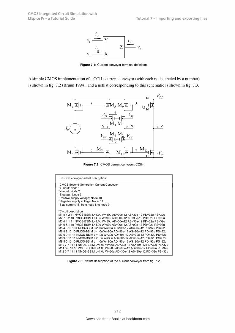
CMOS Integrated Circuit Simulation with LTspice IV – a Tutorial Guide
212
Tutorial 7 – Importing and exporting filesCMOS Integrated Circuit Simulation with LTspice IV Tutorial 7
Figure 7.1: Current conveyor terminal definition.
A simple CMOS implementation of a CCII+ current conveyor (with each node labeled by a number)is shown in fig. 7.2 (Bruun 1994), and a netlist corresponding to this schematic is shown in fig. 7.3.
Figure 7.2: CMOS current conveyor, CCII+.
Current conveyor netlist description.
*CMOS Second Generation Current Conveyor*Y-input: Node 1*X-input: Node 2*Z-output: Node 3*Positive supply voltage: Node 10*Negative supply voltage: Node 11*Bias current: IB, from node 8 to node 9
*Circuit descriptionM1 5 4 2 11 NMOS-BSIM L=1.0u W=30u AD=30e-12 AS=30e-12 PD=32u PS=32uM2 7 6 2 10 PMOS-BSIM L=1.0u W=90u AD=90e-12 AS=90e-12 PD=92u PS=92uM3 4 4 1 11 NMOS-BSIM L=1.0u W=30u AD=30e-12 AS=30e-12 PD=32u PS=32uM4 6 6 1 10 PMOS-BSIM L=1.0u W=90u AD=90e-12 AS=90e-12 PD=92u PS=92uM5 4 8 10 10 PMOS-BSIM L=1.0u W=90u AD=90e-12 AS=90e-12 PD=92u PS=92uM6 8 8 10 10 PMOS-BSIM L=1.0u W=90u AD=90e-12 AS=90e-12 PD=92u PS=92uM7 6 9 11 11 NMOS-BSIM L=1.0u W=30u AD=30e-12 AS=30e-12 PD=32u PS=32uM8 9 9 11 11 NMOS-BSIM L=1.0u W=30u AD=30e-12 AS=30e-12 PD=32u PS=32uM9 5 5 10 10 PMOS-BSIM L=1.0u W=90u AD=90e-12 AS=90e-12 PD=92u PS=92uM10 7 7 11 11 NMOS-BSIM L=1.0u W=30u AD=30e-12 AS=30e-12 PD=32u PS=32uM11 3 5 10 10 PMOS-BSIM L=1.0u W=90u AD=90e-12 AS=90e-12 PD=92u PS=92uM12 3 7 11 11 NMOS-BSIM L=1.0u W=30u AD=30e-12 AS=30e-12 PD=32u PS=32u
Figure 7.3: Netlist description of the current conveyor from fig. 7.2.
212
Download free eBooks at bookboon.com
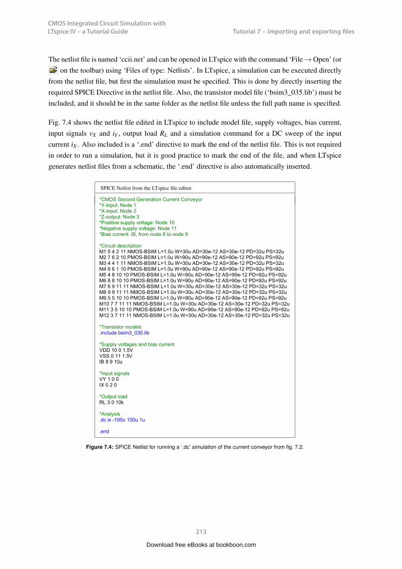
CMOS Integrated Circuit Simulation with LTspice IV – a Tutorial Guide
213
Tutorial 7 – Importing and exporting filesCMOS Integrated Circuit Simulation with LTspice IV Tutorial 7
The netlist file is named ‘ccii.net’ and can be opened in LTspice with the command ‘File → Open’ (oron the toolbar) using ‘Files of type: Netlists’. In LTspice, a simulation can be executed directly
from the netlist file, but first the simulation must be specified. This is done by directly inserting therequired SPICE Directive in the netlist file. Also, the transistor model file (‘bsim3_035.lib’) must beincluded, and it should be in the same folder as the netlist file unless the full path name is specified.
Fig. 7.4 shows the netlist file edited in LTspice to include model file, supply voltages, bias current,input signals vX and iY , output load RL and a simulation command for a DC sweep of the inputcurrent iX . Also included is a ‘.end’ directive to mark the end of the netlist file. This is not requiredin order to run a simulation, but it is good practice to mark the end of the file, and when LTspicegenerates netlist files from a schematic, the ‘.end’ directive is also automatically inserted.
SPICE Netlist from the LTspice file editor.
*CMOS Second Generation Current Conveyor*Y-input: Node 1*X-input: Node 2*Z-output: Node 3*Positive supply voltage: Node 10*Negative supply voltage: Node 11*Bias current: IB, from node 8 to node 9
*Circuit descriptionM1 5 4 2 11 NMOS-BSIM L=1.0u W=30u AD=30e-12 AS=30e-12 PD=32u PS=32uM2 7 6 2 10 PMOS-BSIM L=1.0u W=90u AD=90e-12 AS=90e-12 PD=92u PS=92uM3 4 4 1 11 NMOS-BSIM L=1.0u W=30u AD=30e-12 AS=30e-12 PD=32u PS=32uM4 6 6 1 10 PMOS-BSIM L=1.0u W=90u AD=90e-12 AS=90e-12 PD=92u PS=92uM5 4 8 10 10 PMOS-BSIM L=1.0u W=90u AD=90e-12 AS=90e-12 PD=92u PS=92uM6 8 8 10 10 PMOS-BSIM L=1.0u W=90u AD=90e-12 AS=90e-12 PD=92u PS=92uM7 6 9 11 11 NMOS-BSIM L=1.0u W=30u AD=30e-12 AS=30e-12 PD=32u PS=32uM8 9 9 11 11 NMOS-BSIM L=1.0u W=30u AD=30e-12 AS=30e-12 PD=32u PS=32uM9 5 5 10 10 PMOS-BSIM L=1.0u W=90u AD=90e-12 AS=90e-12 PD=92u PS=92uM10 7 7 11 11 NMOS-BSIM L=1.0u W=30u AD=30e-12 AS=30e-12 PD=32u PS=32uM11 3 5 10 10 PMOS-BSIM L=1.0u W=90u AD=90e-12 AS=90e-12 PD=92u PS=92uM12 3 7 11 11 NMOS-BSIM L=1.0u W=30u AD=30e-12 AS=30e-12 PD=32u PS=32u
*Transistor models.include bsim3_035.lib
*Supply voltages and bias currentVDD 10 0 1.5VVSS 0 11 1.5VIB 8 9 10u
*Input signalsVY 1 0 0IX 0 2 0
*Output loadRL 3 0 10k
*Analysis.dc ix -100u 100u 1u
.end
Figure 7.4: SPICE Netlist for running a ‘.dc’ simulation of the current conveyor from fig. 7.2.
213
Download free eBooks at bookboon.com

CMOS Integrated Circuit Simulation with LTspice IV – a Tutorial Guide
214
Tutorial 7 – Importing and exporting filesCMOS Integrated Circuit Simulation with LTspice IV Tutorial 7
The simulation is run directly from the SPICE Netlist using the command ‘Simulate → Run’ orusing the ‘Run’-symbol on the toolbar. Fig. 7.5 shows the result of the simulation. The traces tobe displayed are selected in the plot window using the command ‘Plot Settings → Add trace’ or thecommand ‘Plot Settings → Visible Traces’. The command ‘Visible Traces’ is also available withthe netlist window active (’View → Visible Traces’) and on the toolbar, symbol , also see page23. Fig. 7.5 shows the input current iX and the output current iZ = −I(RL). Obviously, the outputcurrent is almost the same as the input current as expected from (7.1).
Figure 7.5: Simulated output current iZ =−I(RL) for the current conveyor from the SPICE Netlist shown in fig. 7.4.
214
Download free eBooks at bookboon.com
Click on the ad to read moreClick on the ad to read moreClick on the ad to read moreClick on the ad to read moreClick on the ad to read moreClick on the ad to read moreClick on the ad to read moreClick on the ad to read moreClick on the ad to read moreClick on the ad to read moreClick on the ad to read moreClick on the ad to read moreClick on the ad to read moreClick on the ad to read moreClick on the ad to read moreClick on the ad to read moreClick on the ad to read moreClick on the ad to read moreClick on the ad to read moreClick on the ad to read moreClick on the ad to read moreClick on the ad to read moreClick on the ad to read moreClick on the ad to read moreClick on the ad to read moreClick on the ad to read moreClick on the ad to read moreClick on the ad to read moreClick on the ad to read moreClick on the ad to read moreClick on the ad to read moreClick on the ad to read moreClick on the ad to read moreClick on the ad to read moreClick on the ad to read moreClick on the ad to read moreClick on the ad to read moreClick on the ad to read moreClick on the ad to read moreClick on the ad to read moreClick on the ad to read moreClick on the ad to read moreClick on the ad to read moreClick on the ad to read moreClick on the ad to read moreClick on the ad to read moreClick on the ad to read moreClick on the ad to read moreClick on the ad to read moreClick on the ad to read moreClick on the ad to read moreClick on the ad to read moreClick on the ad to read moreClick on the ad to read moreClick on the ad to read moreClick on the ad to read moreClick on the ad to read moreClick on the ad to read moreClick on the ad to read moreClick on the ad to read moreClick on the ad to read moreClick on the ad to read moreClick on the ad to read moreClick on the ad to read moreClick on the ad to read moreClick on the ad to read moreClick on the ad to read moreClick on the ad to read moreClick on the ad to read moreClick on the ad to read moreClick on the ad to read moreClick on the ad to read moreClick on the ad to read moreClick on the ad to read more
- ©
Pho
tono
nsto
p
> Apply now
redefine your future
AxA globAl grAduAte progrAm 2015
axa_ad_grad_prog_170x115.indd 1 19/12/13 16:36
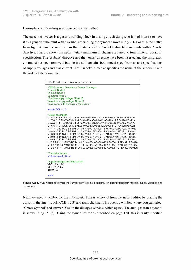
CMOS Integrated Circuit Simulation with LTspice IV – a Tutorial Guide
215
Tutorial 7 – Importing and exporting filesCMOS Integrated Circuit Simulation with LTspice IV Tutorial 7
Example 7.2: Creating a subcircuit from a netlist.
The current conveyor is a generic building block in analog circuit design, so it is of interest to haveit as a generic subcircuit with a symbol resembling the symbol shown in fig. 7.1. For this, the netlistfrom fig. 7.4 must be modified so that it starts with a ‘.subckt’ directive and ends with a ‘.ends’directive. Fig. 7.6 shows the netlist with a minimum of changes required to turn it into a subcircuitspecification. The ‘.subckt’ directive and the ‘.ends’ directive have been inserted and the simulationcommand has been removed, but the file still contains both model specifications and specificationsof supply voltages and bias current. The ‘.subckt’ directive specifies the name of the subcircuit andthe order of the terminals.
SPICE Netlist, current conveyor subcircuit.
*CMOS Second Generation Current Conveyor*Y-input: Node 1*X-input: Node 2*Z-output: Node 3*Positive supply voltage: Node 10*Negative supply voltage: Node 11*Bias current: IB, from node 8 to node 9
.subckt CCII 1 2 3
*Circuit descriptionM1 5 4 2 11 NMOS-BSIM L=1.0u W=30u AD=30e-12 AS=30e-12 PD=32u PS=32uM2 7 6 2 10 PMOS-BSIM L=1.0u W=90u AD=90e-12 AS=90e-12 PD=92u PS=92uM3 4 4 1 11 NMOS-BSIM L=1.0u W=30u AD=30e-12 AS=30e-12 PD=32u PS=32uM4 6 6 1 10 PMOS-BSIM L=1.0u W=90u AD=90e-12 AS=90e-12 PD=92u PS=92uM5 4 8 10 10 PMOS-BSIM L=1.0u W=90u AD=90e-12 AS=90e-12 PD=92u PS=92uM6 8 8 10 10 PMOS-BSIM L=1.0u W=90u AD=90e-12 AS=90e-12 PD=92u PS=92uM7 6 9 11 11 NMOS-BSIM L=1.0u W=30u AD=30e-12 AS=30e-12 PD=32u PS=32uM8 9 9 11 11 NMOS-BSIM L=1.0u W=30u AD=30e-12 AS=30e-12 PD=32u PS=32uM9 5 5 10 10 PMOS-BSIM L=1.0u W=90u AD=90e-12 AS=90e-12 PD=92u PS=92uM10 7 7 11 11 NMOS-BSIM L=1.0u W=30u AD=30e-12 AS=30e-12 PD=32u PS=32uM11 3 5 10 10 PMOS-BSIM L=1.0u W=90u AD=90e-12 AS=90e-12 PD=92u PS=92uM12 3 7 11 11 NMOS-BSIM L=1.0u W=30u AD=30e-12 AS=30e-12 PD=32u PS=32u
*Transistor models.include bsim3_035.lib
*Supply voltages and bias currentVDD 10 0 1.5VVSS 0 11 1.5VIB 8 9 10u
.ends
Figure 7.6: SPICE Netlist specifying the current conveyor as a subcircuit including transistor models, supply voltages andbias current.
Next, we need a symbol for the subcircuit. This is achieved from the netlist editor by placing thecursor in the line ‘.subckt CCII 1 2 3’ and right clicking. This opens a window where you can select‘Create Symbol’ and answer ‘Yes’ in the dialogue window which opens. The auto-generated symbolis shown in fig. 7.7(a). Using the symbol editor as described on page 150, this is easily modified
215
Download free eBooks at bookboon.com
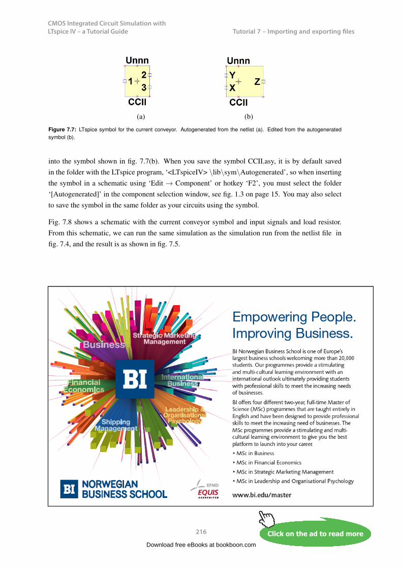
CMOS Integrated Circuit Simulation with LTspice IV – a Tutorial Guide
216
Tutorial 7 – Importing and exporting filesCMOS Integrated Circuit Simulation with LTspice IV Tutorial 7
(a) (b)
Figure 7.7: LTspice symbol for the current conveyor. Autogenerated from the netlist (a). Edited from the autogeneratedsymbol (b).
into the symbol shown in fig. 7.7(b). When you save the symbol CCII.asy, it is by default savedin the folder with the LTspice program, ‘<LTspiceIV> \lib\sym\Autogenerated’, so when insertingthe symbol in a schematic using ‘Edit → Component’ or hotkey ‘F2’, you must select the folder‘[Autogenerated]’ in the component selection window, see fig. 1.3 on page 15. You may also selectto save the symbol in the same folder as your circuits using the symbol.
Fig. 7.8 shows a schematic with the current conveyor symbol and input signals and load resistor.From this schematic, we can run the same simulation as the simulation run from the netlist file infig. 7.4, and the result is as shown in fig. 7.5.
The subcircuit defined in fig. 7.6 includes both the transistor model file, the supply voltages and the
216
Download free eBooks at bookboon.com
Click on the ad to read moreClick on the ad to read moreClick on the ad to read moreClick on the ad to read moreClick on the ad to read moreClick on the ad to read moreClick on the ad to read moreClick on the ad to read moreClick on the ad to read moreClick on the ad to read moreClick on the ad to read moreClick on the ad to read moreClick on the ad to read moreClick on the ad to read moreClick on the ad to read moreClick on the ad to read moreClick on the ad to read moreClick on the ad to read moreClick on the ad to read moreClick on the ad to read moreClick on the ad to read moreClick on the ad to read moreClick on the ad to read moreClick on the ad to read moreClick on the ad to read moreClick on the ad to read moreClick on the ad to read moreClick on the ad to read moreClick on the ad to read moreClick on the ad to read moreClick on the ad to read moreClick on the ad to read moreClick on the ad to read moreClick on the ad to read moreClick on the ad to read moreClick on the ad to read moreClick on the ad to read moreClick on the ad to read moreClick on the ad to read moreClick on the ad to read moreClick on the ad to read moreClick on the ad to read moreClick on the ad to read moreClick on the ad to read moreClick on the ad to read moreClick on the ad to read moreClick on the ad to read moreClick on the ad to read moreClick on the ad to read moreClick on the ad to read moreClick on the ad to read moreClick on the ad to read moreClick on the ad to read moreClick on the ad to read moreClick on the ad to read moreClick on the ad to read moreClick on the ad to read moreClick on the ad to read moreClick on the ad to read moreClick on the ad to read moreClick on the ad to read moreClick on the ad to read moreClick on the ad to read moreClick on the ad to read moreClick on the ad to read moreClick on the ad to read moreClick on the ad to read moreClick on the ad to read moreClick on the ad to read moreClick on the ad to read moreClick on the ad to read moreClick on the ad to read moreClick on the ad to read moreClick on the ad to read moreClick on the ad to read more
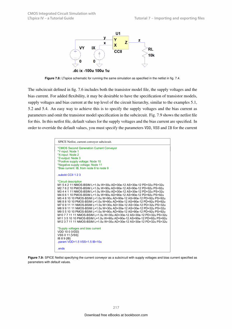
CMOS Integrated Circuit Simulation with LTspice IV – a Tutorial Guide
217
Tutorial 7 – Importing and exporting filesCMOS Integrated Circuit Simulation with LTspice IV Tutorial 7
Figure 7.8: LTspice schematic for running the same simulation as specified in the netlist in fig. 7.4.
bias current. For added flexibility, it may be desirable to have the specification of transistor models,supply voltages and bias current at the top level of the circuit hierarchy, similar to the examples 5.1,5.2 and 5.4. An easy way to achieve this is to specify the supply voltages and the bias current asparameters and omit the transistor model specification in the subcircuit. Fig. 7.9 shows the netlist filefor this. In this netlist file, default values for the supply voltages and the bias current are specified. Inorder to override the default values, you must specify the parameters VDD, VSS and IB for the current
SPICE Netlist, current conveyor subcircuit.
*CMOS Second Generation Current Conveyor*Y-input: Node 1*X-input: Node 2*Z-output: Node 3*Positive supply voltage: Node 10*Negative supply voltage: Node 11*Bias current: IB, from node 8 to node 9
.subckt CCII 1 2 3
*Circuit descriptionM1 5 4 2 11 NMOS-BSIM L=1.0u W=30u AD=30e-12 AS=30e-12 PD=32u PS=32uM2 7 6 2 10 PMOS-BSIM L=1.0u W=90u AD=90e-12 AS=90e-12 PD=92u PS=92uM3 4 4 1 11 NMOS-BSIM L=1.0u W=30u AD=30e-12 AS=30e-12 PD=32u PS=32uM4 6 6 1 10 PMOS-BSIM L=1.0u W=90u AD=90e-12 AS=90e-12 PD=92u PS=92uM5 4 8 10 10 PMOS-BSIM L=1.0u W=90u AD=90e-12 AS=90e-12 PD=92u PS=92uM6 8 8 10 10 PMOS-BSIM L=1.0u W=90u AD=90e-12 AS=90e-12 PD=92u PS=92uM7 6 9 11 11 NMOS-BSIM L=1.0u W=30u AD=30e-12 AS=30e-12 PD=32u PS=32uM8 9 9 11 11 NMOS-BSIM L=1.0u W=30u AD=30e-12 AS=30e-12 PD=32u PS=32uM9 5 5 10 10 PMOS-BSIM L=1.0u W=90u AD=90e-12 AS=90e-12 PD=92u PS=92uM10 7 7 11 11 NMOS-BSIM L=1.0u W=30u AD=30e-12 AS=30e-12 PD=32u PS=32uM11 3 5 10 10 PMOS-BSIM L=1.0u W=90u AD=90e-12 AS=90e-12 PD=92u PS=92uM12 3 7 11 11 NMOS-BSIM L=1.0u W=30u AD=30e-12 AS=30e-12 PD=32u PS=32u
*Supply voltages and bias currentVDD 10 0 VDDVSS 0 11 VSSIB 8 9 IB.param VDD=1.5 VSS=1.5 IB=10u
.ends
Figure 7.9: SPICE Netlist specifying the current conveyor as a subcircuit with supply voltages and bias current specified asparameters with default values.
217
CMOS Integrated Circuit Simulation with LTspice IV Tutorial 7
(a) (b)
Figure 7.7: LTspice symbol for the current conveyor. Autogenerated from the netlist (a). Edited from the autogeneratedsymbol (b).
into the symbol shown in fig. 7.7(b). When you save the symbol CCII.asy, it is by default savedin the folder with the LTspice program, ‘<LTspiceIV> \lib\sym\Autogenerated’, so when insertingthe symbol in a schematic using ‘Edit → Component’ or hotkey ‘F2’, you must select the folder‘[Autogenerated]’ in the component selection window, see fig. 1.3 on page 15. You may also selectto save the symbol in the same folder as your circuits using the symbol.
Fig. 7.8 shows a schematic with the current conveyor symbol and input signals and load resistor.From this schematic, we can run the same simulation as the simulation run from the netlist file infig. 7.4, and the result is as shown in fig. 7.5.
The subcircuit defined in fig. 7.6 includes both the transistor model file, the supply voltages and the
216
Download free eBooks at bookboon.com
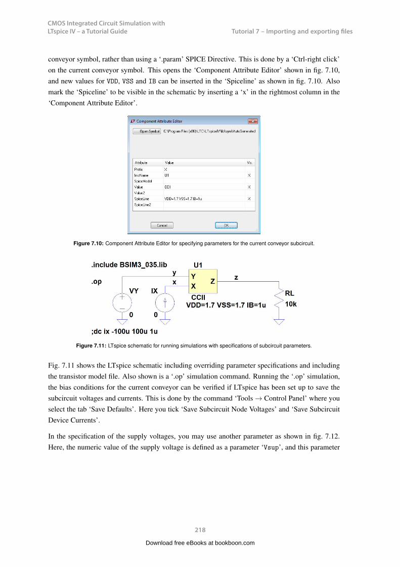
CMOS Integrated Circuit Simulation with LTspice IV – a Tutorial Guide
218
Tutorial 7 – Importing and exporting filesCMOS Integrated Circuit Simulation with LTspice IV Tutorial 7
conveyor symbol, rather than using a ‘.param’ SPICE Directive. This is done by a ‘Ctrl-right click’on the current conveyor symbol. This opens the ‘Component Attribute Editor’ shown in fig. 7.10,and new values for VDD, VSS and IB can be inserted in the ‘Spiceline’ as shown in fig. 7.10. Alsomark the ‘Spiceline’ to be visible in the schematic by inserting a ‘x’ in the rightmost column in the‘Component Attribute Editor’.
Figure 7.10: Component Attribute Editor for specifying parameters for the current conveyor subcircuit.
Figure 7.11: LTspice schematic for running simulations with specifications of subcircuit parameters.
Fig. 7.11 shows the LTspice schematic including overriding parameter specifications and includingthe transistor model file. Also shown is a ‘.op’ simulation command. Running the ‘.op’ simulation,the bias conditions for the current conveyor can be verified if LTspice has been set up to save thesubcircuit voltages and currents. This is done by the command ‘Tools → Control Panel’ where youselect the tab ‘Save Defaults’. Here you tick ‘Save Subcircuit Node Voltages’ and ‘Save SubcircuitDevice Currents’.
In the specification of the supply voltages, you may use another parameter as shown in fig. 7.12.Here, the numeric value of the supply voltage is defined as a parameter ‘Vsup’, and this parameter
218
Download free eBooks at bookboon.com

CMOS Integrated Circuit Simulation with LTspice IV – a Tutorial Guide
219
Tutorial 7 – Importing and exporting filesCMOS Integrated Circuit Simulation with LTspice IV Tutorial 7
is stepped from 1.3 V to 1.7 V using a ‘.step param’ directive. Also the value of the load resistorhas been changed to 20 kΩ. With this value of RL, the Z-output cannot deliver an output currentof 100 µA because the output voltage exceeds the supply rails for iZ = ±100 µA. This is shownin fig. 7.13 where the output current is plotted versus the input current for three different values ofsupply voltage.
Figure 7.12: LTspice schematic for running simulations with different values of supply voltage.
An alternative way for specifying supply voltages and bias current at top level of the circuit hierarchyis by introducing terminals for the supply voltages and the bias current in the schematic symbol. Thisis achieved by first specifying the terminals in the netlist description as shown in fig. 7.14 and thendesigning a symbol including these terminals in the same way as the symbol from fig. 7.7.
219
Download free eBooks at bookboon.com
Click on the ad to read moreClick on the ad to read moreClick on the ad to read moreClick on the ad to read moreClick on the ad to read moreClick on the ad to read moreClick on the ad to read moreClick on the ad to read moreClick on the ad to read moreClick on the ad to read moreClick on the ad to read moreClick on the ad to read moreClick on the ad to read moreClick on the ad to read moreClick on the ad to read moreClick on the ad to read moreClick on the ad to read moreClick on the ad to read moreClick on the ad to read moreClick on the ad to read moreClick on the ad to read moreClick on the ad to read moreClick on the ad to read moreClick on the ad to read moreClick on the ad to read moreClick on the ad to read moreClick on the ad to read moreClick on the ad to read moreClick on the ad to read moreClick on the ad to read moreClick on the ad to read moreClick on the ad to read moreClick on the ad to read moreClick on the ad to read moreClick on the ad to read moreClick on the ad to read moreClick on the ad to read moreClick on the ad to read moreClick on the ad to read moreClick on the ad to read moreClick on the ad to read moreClick on the ad to read moreClick on the ad to read moreClick on the ad to read moreClick on the ad to read moreClick on the ad to read moreClick on the ad to read moreClick on the ad to read moreClick on the ad to read moreClick on the ad to read moreClick on the ad to read moreClick on the ad to read moreClick on the ad to read moreClick on the ad to read moreClick on the ad to read moreClick on the ad to read moreClick on the ad to read moreClick on the ad to read moreClick on the ad to read moreClick on the ad to read moreClick on the ad to read moreClick on the ad to read moreClick on the ad to read moreClick on the ad to read moreClick on the ad to read moreClick on the ad to read moreClick on the ad to read moreClick on the ad to read moreClick on the ad to read moreClick on the ad to read moreClick on the ad to read moreClick on the ad to read moreClick on the ad to read moreClick on the ad to read moreClick on the ad to read moreClick on the ad to read more
Get Help Now
Go to www.helpmyassignment.co.uk for more info
Need help with yourdissertation?Get in-depth feedback & advice from experts in your topic area. Find out what you can do to improvethe quality of your dissertation!
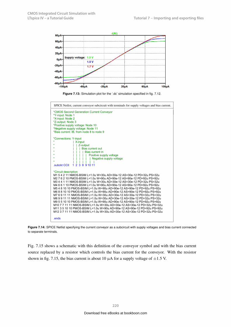
CMOS Integrated Circuit Simulation with LTspice IV – a Tutorial Guide
220
Tutorial 7 – Importing and exporting filesCMOS Integrated Circuit Simulation with LTspice IV Tutorial 7
Figure 7.13: Simulation plot for the ‘.dc’ simulation specified in fig. 7.12.
SPICE Netlist, current conveyor subcircuit with terminals for supply voltages and bias current.
*CMOS Second Generation Current Conveyor*Y-input: Node 1*X-input: Node 2*Z-output: Node 3*Positive supply voltage: Node 10*Negative supply voltage: Node 11*Bias current: IB, from node 8 to node 9
*Connections: Y-input* | X-input* | | Z-output* | | | Bias current out* | | | | Bias current in* | | | | | Positive supply voltage* | | | | | | Negative supply voltage* | | | | | | |.subckt CCII 1 2 3 8 9 10 11
*Circuit descriptionM1 5 4 2 11 NMOS-BSIM L=1.0u W=30u AD=30e-12 AS=30e-12 PD=32u PS=32uM2 7 6 2 10 PMOS-BSIM L=1.0u W=90u AD=90e-12 AS=90e-12 PD=92u PS=92uM3 4 4 1 11 NMOS-BSIM L=1.0u W=30u AD=30e-12 AS=30e-12 PD=32u PS=32uM4 6 6 1 10 PMOS-BSIM L=1.0u W=90u AD=90e-12 AS=90e-12 PD=92u PS=92uM5 4 8 10 10 PMOS-BSIM L=1.0u W=90u AD=90e-12 AS=90e-12 PD=92u PS=92uM6 8 8 10 10 PMOS-BSIM L=1.0u W=90u AD=90e-12 AS=90e-12 PD=92u PS=92uM7 6 9 11 11 NMOS-BSIM L=1.0u W=30u AD=30e-12 AS=30e-12 PD=32u PS=32uM8 9 9 11 11 NMOS-BSIM L=1.0u W=30u AD=30e-12 AS=30e-12 PD=32u PS=32uM9 5 5 10 10 PMOS-BSIM L=1.0u W=90u AD=90e-12 AS=90e-12 PD=92u PS=92uM10 7 7 11 11 NMOS-BSIM L=1.0u W=30u AD=30e-12 AS=30e-12 PD=32u PS=32uM11 3 5 10 10 PMOS-BSIM L=1.0u W=90u AD=90e-12 AS=90e-12 PD=92u PS=92uM12 3 7 11 11 NMOS-BSIM L=1.0u W=30u AD=30e-12 AS=30e-12 PD=32u PS=32u
.ends
Figure 7.14: SPICE Netlist specifying the current conveyor as a subcircuit with supply voltages and bias current connectedto separate terminals.
Fig. 7.15 shows a schematic with this definition of the conveyor symbol and with the bias currentsource replaced by a resistor which controls the bias current for the conveyor. With the resistorshown in fig. 7.15, the bias current is about 10 µA for a supply voltage of ±1.5 V.
220
Download free eBooks at bookboon.com
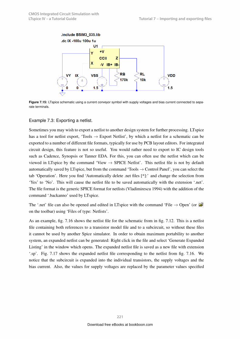
CMOS Integrated Circuit Simulation with LTspice IV – a Tutorial Guide
221
Tutorial 7 – Importing and exporting filesCMOS Integrated Circuit Simulation with LTspice IV Tutorial 7
Figure 7.15: LTspice schematic using a current conveyor symbol with supply voltages and bias current connected to sepa-rate terminals.
Example 7.3: Exporting a netlist.
Sometimes you may wish to export a netlist to another design system for further processing. LTspicehas a tool for netlist export, ‘Tools → Export Netlist’, by which a netlist for a schematic can beexported to a number of different file formats, typically for use by PCB layout editors. For integratedcircuit design, this feature is not so useful. You would rather need to export to IC design toolssuch as Cadence, Synopsis or Tanner EDA. For this, you can often use the netlist which can beviewed in LTspice by the command ‘View → SPICE Netlist’. This netlist file is not by defaultautomatically saved by LTspice, but from the command ‘Tools → Control Panel’, you can select thetab ‘Operation’. Here you find ‘Automatically delete .net files [*]:’ and change the selection from‘Yes’ to ‘No’. This will cause the netlist file to be saved automatically with the extension ‘.net’.The file format is the generic SPICE format for netlists (Vladimirescu 1994) with the addition of thecommand ‘.backanno’ used by LTspice.
The ‘.net’ file can also be opened and edited in LTspice with the command ‘File → Open’ (oron the toolbar) using ‘Files of type: Netlists’.
As an example, fig. 7.16 shows the netlist file for the schematic from in fig. 7.12. This is a netlistfile containing both references to a transistor model file and to a subcircuit, so without these filesit cannot be used by another Spice simulator. In order to obtain maximum portability to anothersystem, an expanded netlist can be generated: Right click in the file and select ‘Generate ExpandedListing’ in the window which opens. The expanded netlist file is saved as a new file with extension‘.sp’. Fig. 7.17 shows the expanded netlist file corresponding to the netlist from fig. 7.16. Wenotice that the subcircuit is expanded into the individual transistors, the supply voltages and thebias current. Also, the values for supply voltages are replaced by the parameter values specified
221
Download free eBooks at bookboon.com

CMOS Integrated Circuit Simulation with LTspice IV – a Tutorial Guide
222
Tutorial 7 – Importing and exporting filesCMOS Integrated Circuit Simulation with LTspice IV Tutorial 7
SPICE Netlist from schematic.
* M:\LTspice\Tutorial07\fig7_12.ascRL z 0 20kVY y 0 0IX 0 x 0XU1 y x z CCII VDD=Vsup VSS=Vsup IB=1u.dc ix -100u 100u 1u.include BSIM3_035.lib;op.step param Vsup 1.3 1.7 0.2.lib M:\LTspice\Tutorial07\ccii.net.backanno.end
Figure 7.16: SPICE Netlist for the circuit from fig. 7.12.
as the first step in the ‘.step param’ command. Further, the ‘.include BSIM3_035.lib’ command isexpanded into the two transistor models. Each of the models is collapsed into a single, very longline in the expanded netlist file, so in fig. 7.17 only the start of the model lines is shown. Finally, the‘.backanno’ command has been removed.
The expanded netlist also contains the simulation command, so a simulation can be run directly fromthe netlist, but the ‘.step param’ command is not included. Instead, the parameter values for the firststep are inserted, and the simulation will show only the first step. Fig. 7.18 shows the simulation runfrom the netlist. It may be compared to the simulation shown in fig. 7.13 run from the schematic.
222
Download free eBooks at bookboon.com
Click on the ad to read moreClick on the ad to read moreClick on the ad to read moreClick on the ad to read moreClick on the ad to read moreClick on the ad to read moreClick on the ad to read moreClick on the ad to read moreClick on the ad to read moreClick on the ad to read moreClick on the ad to read moreClick on the ad to read moreClick on the ad to read moreClick on the ad to read moreClick on the ad to read moreClick on the ad to read moreClick on the ad to read moreClick on the ad to read moreClick on the ad to read moreClick on the ad to read moreClick on the ad to read moreClick on the ad to read moreClick on the ad to read moreClick on the ad to read moreClick on the ad to read moreClick on the ad to read moreClick on the ad to read moreClick on the ad to read moreClick on the ad to read moreClick on the ad to read moreClick on the ad to read moreClick on the ad to read moreClick on the ad to read moreClick on the ad to read moreClick on the ad to read moreClick on the ad to read moreClick on the ad to read moreClick on the ad to read moreClick on the ad to read moreClick on the ad to read moreClick on the ad to read moreClick on the ad to read moreClick on the ad to read moreClick on the ad to read moreClick on the ad to read moreClick on the ad to read moreClick on the ad to read moreClick on the ad to read moreClick on the ad to read moreClick on the ad to read moreClick on the ad to read moreClick on the ad to read moreClick on the ad to read moreClick on the ad to read moreClick on the ad to read moreClick on the ad to read moreClick on the ad to read moreClick on the ad to read moreClick on the ad to read moreClick on the ad to read moreClick on the ad to read moreClick on the ad to read moreClick on the ad to read moreClick on the ad to read moreClick on the ad to read moreClick on the ad to read moreClick on the ad to read moreClick on the ad to read moreClick on the ad to read moreClick on the ad to read moreClick on the ad to read moreClick on the ad to read moreClick on the ad to read moreClick on the ad to read moreClick on the ad to read moreClick on the ad to read moreClick on the ad to read more
By 2020, wind could provide one-tenth of our planet’s electricity needs. Already today, SKF’s innovative know-how is crucial to running a large proportion of the world’s wind turbines.
Up to 25 % of the generating costs relate to mainte-nance. These can be reduced dramatically thanks to our systems for on-line condition monitoring and automatic lubrication. We help make it more economical to create cleaner, cheaper energy out of thin air.
By sharing our experience, expertise, and creativity, industries can boost performance beyond expectations.
Therefore we need the best employees who can meet this challenge!
The Power of Knowledge Engineering
Brain power
Plug into The Power of Knowledge Engineering.
Visit us at www.skf.com/knowledge
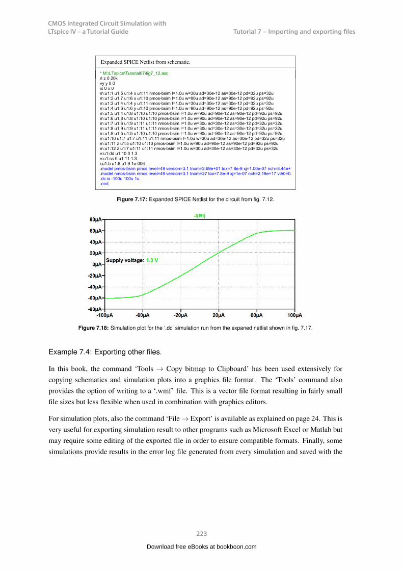
CMOS Integrated Circuit Simulation with LTspice IV – a Tutorial Guide
223
Tutorial 7 – Importing and exporting filesCMOS Integrated Circuit Simulation with LTspice IV Tutorial 7
Expanded SPICE Netlist from schematic.
* M:\LTspice\Tutorial07\fig7_12.ascrl z 0 20kvy y 0 0ix 0 x 0m:u1:1 u1:5 u1:4 x u1:11 nmos-bsim l=1.0u w=30u ad=30e-12 as=30e-12 pd=32u ps=32um:u1:2 u1:7 u1:6 x u1:10 pmos-bsim l=1.0u w=90u ad=90e-12 as=90e-12 pd=92u ps=92um:u1:3 u1:4 u1:4 y u1:11 nmos-bsim l=1.0u w=30u ad=30e-12 as=30e-12 pd=32u ps=32um:u1:4 u1:6 u1:6 y u1:10 pmos-bsim l=1.0u w=90u ad=90e-12 as=90e-12 pd=92u ps=92um:u1:5 u1:4 u1:8 u1:10 u1:10 pmos-bsim l=1.0u w=90u ad=90e-12 as=90e-12 pd=92u ps=92um:u1:6 u1:8 u1:8 u1:10 u1:10 pmos-bsim l=1.0u w=90u ad=90e-12 as=90e-12 pd=92u ps=92um:u1:7 u1:6 u1:9 u1:11 u1:11 nmos-bsim l=1.0u w=30u ad=30e-12 as=30e-12 pd=32u ps=32um:u1:8 u1:9 u1:9 u1:11 u1:11 nmos-bsim l=1.0u w=30u ad=30e-12 as=30e-12 pd=32u ps=32um:u1:9 u1:5 u1:5 u1:10 u1:10 pmos-bsim l=1.0u w=90u ad=90e-12 as=90e-12 pd=92u ps=92um:u1:10 u1:7 u1:7 u1:11 u1:11 nmos-bsim l=1.0u w=30u ad=30e-12 as=30e-12 pd=32u ps=32um:u1:11 z u1:5 u1:10 u1:10 pmos-bsim l=1.0u w=90u ad=90e-12 as=90e-12 pd=92u ps=92um:u1:12 z u1:7 u1:11 u1:11 nmos-bsim l=1.0u w=30u ad=30e-12 as=30e-12 pd=32u ps=32uv:u1:dd u1:10 0 1.3 v:u1:ss 0 u1:11 1.3 i:u1:b u1:8 u1:9 1e-006.model pmos-bsim pmos level=49 version=3.1 tnom=2.69e+01 tox=7.8e-9 xj=1.00e-07 nch=8.44e+16 vth0=-0.6 k1=4.82e-01 k2=-.model nmos-bsim nmos level=49 version=3.1 tnom=27 tox=7.8e-9 xj=1e-07 nch=2.18e+17 vth0=0.48 k1=6.07e-01 k2=1.24e-03.dc ix -100u 100u 1u.end
Figure 7.17: Expanded SPICE Netlist for the circuit from fig. 7.12.
Figure 7.18: Simulation plot for the ‘.dc’ simulation run from the expaned netlist shown in fig. 7.17.
Example 7.4: Exporting other files.
In this book, the command ‘Tools → Copy bitmap to Clipboard’ has been used extensively forcopying schematics and simulation plots into a graphics file format. The ‘Tools’ command alsoprovides the option of writing to a ‘.wmf’ file. This is a vector file format resulting in fairly smallfile sizes but less flexible when used in combination with graphics editors.
For simulation plots, also the command ‘File → Export’ is available as explained on page 24. This isvery useful for exporting simulation result to other programs such as Microsoft Excel or Matlab butmay require some editing of the exported file in order to ensure compatible formats. Finally, somesimulations provide results in the error log file generated from every simulation and saved with the
223
Download free eBooks at bookboon.com

CMOS Integrated Circuit Simulation with LTspice IV – a Tutorial Guide
224
Tutorial 7 – Importing and exporting filesCMOS Integrated Circuit Simulation with LTspice IV Tutorial 7
extension ‘.log’. An important category is the bias point information for transistors available in the‘.log’ file after running a ‘.op’ simulation. For ‘.op’ simulations (without ‘.step param’ commands),the simulation results (node voltages and device currents) appear directly in a window with the oper-ating point voltages and currents (see page 18), and this information can be copied to the clipboardusing ‘Ctrl-A’ and ‘Ctrl-C’. Also for a ‘.tf’ simulations, the simulation results appear directly in awindow and can be copied to the clipboard.
It is beyond the scope of this book to go into details concerning how to proceed with the differentoutput files in other programs.
224
Download free eBooks at bookboon.com
Click on the ad to read moreClick on the ad to read moreClick on the ad to read moreClick on the ad to read moreClick on the ad to read moreClick on the ad to read moreClick on the ad to read moreClick on the ad to read moreClick on the ad to read moreClick on the ad to read moreClick on the ad to read moreClick on the ad to read moreClick on the ad to read moreClick on the ad to read moreClick on the ad to read moreClick on the ad to read moreClick on the ad to read moreClick on the ad to read moreClick on the ad to read moreClick on the ad to read moreClick on the ad to read moreClick on the ad to read moreClick on the ad to read moreClick on the ad to read moreClick on the ad to read moreClick on the ad to read moreClick on the ad to read moreClick on the ad to read moreClick on the ad to read moreClick on the ad to read moreClick on the ad to read moreClick on the ad to read moreClick on the ad to read moreClick on the ad to read moreClick on the ad to read moreClick on the ad to read moreClick on the ad to read moreClick on the ad to read moreClick on the ad to read moreClick on the ad to read moreClick on the ad to read moreClick on the ad to read moreClick on the ad to read moreClick on the ad to read moreClick on the ad to read moreClick on the ad to read moreClick on the ad to read moreClick on the ad to read moreClick on the ad to read moreClick on the ad to read moreClick on the ad to read moreClick on the ad to read moreClick on the ad to read moreClick on the ad to read moreClick on the ad to read moreClick on the ad to read moreClick on the ad to read moreClick on the ad to read moreClick on the ad to read moreClick on the ad to read moreClick on the ad to read moreClick on the ad to read moreClick on the ad to read moreClick on the ad to read moreClick on the ad to read moreClick on the ad to read moreClick on the ad to read moreClick on the ad to read moreClick on the ad to read moreClick on the ad to read moreClick on the ad to read moreClick on the ad to read moreClick on the ad to read moreClick on the ad to read moreClick on the ad to read moreClick on the ad to read moreClick on the ad to read moreClick on the ad to read more

CMOS Integrated Circuit Simulation with LTspice IV – a Tutorial Guide
225
Tutorial 7 – Importing and exporting filesCMOS Integrated Circuit Simulation with LTspice IV Tutorial 7
Hints and pitfalls
– LTspice accepts Spice netlists which are compatible with the general syntax for Spicenetlists.
– Simulations can be run directly from a netlist file.
– LTspice generates a Spice netlist format which is compatible with the general syntax forSpice netlists.
– The SPICE Netlist for a schematic is automatically saved with a ‘.net’ file extension onlyif this option is selected in the ‘Tools → Control Panel’ tab for ‘Operation’.
– An expanded netlist file (with file extension ‘.sp’) including subcircuits and models can begenerated from a netlist file by selecting ‘Generate Expanded Listing’ when ‘right-clicking’in the netlist file.
– An expanded netlist file ensures maximum portability to other systems.
– A subcircuit may be generated from a netlist file by inserting a ‘.subckt’ command and a‘.ends’ command.
– A subcircuit symbol may be generated automatically from a netlist by ‘right-clicking’ inthe ‘.subckt’ command line.
– A subcircuit symbol generated from a netlist is by default saved in the folder with theLTspice program, ‘<LTspiceIV> \lib\sym\Autogenerated’.
– A subcircuit symbol generated automatically from a schematic is by default saved in thesame folder as the subcircuit schematic, see page 149.
– Do not use the same filename for a subcircuit and a circuit at a higher level in the circuithierarchy.
225
Download free eBooks at bookboon.com

CMOS Integrated Circuit Simulation with LTspice IV – a Tutorial Guide
226
Tutorial 7 – Importing and exporting filesCMOS Integrated Circuit Simulation with LTspice IV Tutorial 7
References
Bruun, E. 1994, ‘CMOS Current Conveyors’, pp. 632-641 (Chapter 11.5) in: Toumazou, C., Bat-tersby, N. and Porta, S., Circuits & Systems Tutorials, pre-conference tutorials at IEEE InternationalSymposium on Circuits and Systems, London, May/June 1994.
Sedra, AS. & Smith, KC. 1970, ‘A Second Generation Current Conveyor and its Applications’, IEEETrans. Circuit Theory vol. CT-17, No. 1, pp. 132-134.
Vladimirescu, A. 1994, The SPICE book, First Edition, John Wiley & Sons, Hoboken, USA.
226
Download free eBooks at bookboon.com

CMOS Integrated Circuit Simulation with LTspice IV – a Tutorial Guide
227
Tutorial 7 – Importing and exporting filesCMOS Integrated Circuit Simulation with LTspice IV Tutorial 7
Problems
7.1
*Differential NMOS pair with *resistive load and differential output
*Noninverting input: Node 3*Inverting input: Node 2*Noninverting output: Node 4*Inverting output: Node 5*Supply voltage: Node 1*Bias current: IB from node 6 to ground
*Circuit descriptionR1 1 4 2.7kR2 1 5 2.7kM1 4 2 6 0 NMOS-BSIM L=0.7u W=16uM2 5 3 6 0 NMOS-BSIM L=0.7u W=16u
Figure P7.1
Fig. P7.1 shows a netlist for a differ-ential NMOS pair with differential out-put. Create a netlist file for LTspicefor simulating the circuit with a supplyvoltage of 3 V, a bias current of 250 µAand a common mode input voltage of1.5 V. Use the BSIM3 transistor modelfrom fig. 3.10 on page 77. Find the biasvalues of the output voltages and thesmall signal differential gain.
227
Download free eBooks at bookboon.com
Click on the ad to read moreClick on the ad to read moreClick on the ad to read moreClick on the ad to read moreClick on the ad to read moreClick on the ad to read moreClick on the ad to read moreClick on the ad to read moreClick on the ad to read moreClick on the ad to read moreClick on the ad to read moreClick on the ad to read moreClick on the ad to read moreClick on the ad to read moreClick on the ad to read moreClick on the ad to read moreClick on the ad to read moreClick on the ad to read moreClick on the ad to read moreClick on the ad to read moreClick on the ad to read moreClick on the ad to read moreClick on the ad to read moreClick on the ad to read moreClick on the ad to read moreClick on the ad to read moreClick on the ad to read moreClick on the ad to read moreClick on the ad to read moreClick on the ad to read moreClick on the ad to read moreClick on the ad to read moreClick on the ad to read moreClick on the ad to read moreClick on the ad to read moreClick on the ad to read moreClick on the ad to read moreClick on the ad to read moreClick on the ad to read moreClick on the ad to read moreClick on the ad to read moreClick on the ad to read moreClick on the ad to read moreClick on the ad to read moreClick on the ad to read moreClick on the ad to read moreClick on the ad to read moreClick on the ad to read moreClick on the ad to read moreClick on the ad to read moreClick on the ad to read moreClick on the ad to read moreClick on the ad to read moreClick on the ad to read moreClick on the ad to read moreClick on the ad to read moreClick on the ad to read moreClick on the ad to read moreClick on the ad to read moreClick on the ad to read moreClick on the ad to read moreClick on the ad to read moreClick on the ad to read moreClick on the ad to read moreClick on the ad to read moreClick on the ad to read moreClick on the ad to read moreClick on the ad to read moreClick on the ad to read moreClick on the ad to read moreClick on the ad to read moreClick on the ad to read moreClick on the ad to read moreClick on the ad to read moreClick on the ad to read moreClick on the ad to read moreClick on the ad to read moreClick on the ad to read moreClick on the ad to read more
EXPERIENCE THE POWER OF FULL ENGAGEMENT…
RUN FASTER. RUN LONGER.. RUN EASIER…
READ MORE & PRE-ORDER TODAY WWW.GAITEYE.COM
Challenge the way we run
1349906_A6_4+0.indd 1 22-08-2014 12:56:57
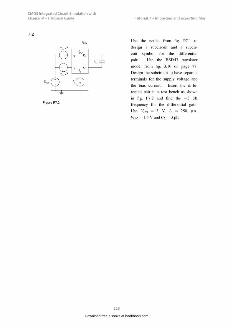
CMOS Integrated Circuit Simulation with LTspice IV – a Tutorial Guide
228
Tutorial 7 – Importing and exporting filesCMOS Integrated Circuit Simulation with LTspice IV Tutorial 7
7.2
Figure P7.2
Use the netlist from fig. P7.1 todesign a subcircuit and a subcir-cuit symbol for the differentialpair. Use the BSIM3 transistormodel from fig. 3.10 on page 77.Design the subcircuit to have separateterminals for the supply voltage andthe bias current. Insert the diffe-rential pair in a test bench as shownin fig. P7.2 and find the −3 dBfrequency for the differential gain.Use VDD = 3 V, IB = 250 µA,VCM = 1.5 V and CL = 3 pF.
228
Download free eBooks at bookboon.com
CMOS Integrated Circuit Simulation with LTspice IV – a Tutorial Guide
229
Tutorial 7 – Importing and exporting filesCMOS Integrated Circuit Simulation with LTspice IV Tutorial 7
7.3Redefine the subcircuit from pro-blem 7.2 to have the transistor chan-nel width as a parameter whichcan be defined at top level.Use the testbench from fig. P7.2 to findthe low frequency gain as a function ofthe channel width for 5 µm≤ W ≤ 30µm. What is the value of the low fre-quency gain for W = 5 µm and W = 30µm?
229
Download free eBooks at bookboon.com
Click on the ad to read moreClick on the ad to read moreClick on the ad to read moreClick on the ad to read moreClick on the ad to read moreClick on the ad to read moreClick on the ad to read moreClick on the ad to read moreClick on the ad to read moreClick on the ad to read moreClick on the ad to read moreClick on the ad to read moreClick on the ad to read moreClick on the ad to read moreClick on the ad to read moreClick on the ad to read moreClick on the ad to read moreClick on the ad to read moreClick on the ad to read moreClick on the ad to read moreClick on the ad to read moreClick on the ad to read moreClick on the ad to read moreClick on the ad to read moreClick on the ad to read moreClick on the ad to read moreClick on the ad to read moreClick on the ad to read moreClick on the ad to read moreClick on the ad to read moreClick on the ad to read moreClick on the ad to read moreClick on the ad to read moreClick on the ad to read moreClick on the ad to read moreClick on the ad to read moreClick on the ad to read moreClick on the ad to read moreClick on the ad to read moreClick on the ad to read moreClick on the ad to read moreClick on the ad to read moreClick on the ad to read moreClick on the ad to read moreClick on the ad to read moreClick on the ad to read moreClick on the ad to read moreClick on the ad to read moreClick on the ad to read moreClick on the ad to read moreClick on the ad to read moreClick on the ad to read moreClick on the ad to read moreClick on the ad to read moreClick on the ad to read moreClick on the ad to read moreClick on the ad to read moreClick on the ad to read moreClick on the ad to read moreClick on the ad to read moreClick on the ad to read moreClick on the ad to read moreClick on the ad to read moreClick on the ad to read moreClick on the ad to read moreClick on the ad to read moreClick on the ad to read moreClick on the ad to read moreClick on the ad to read moreClick on the ad to read moreClick on the ad to read moreClick on the ad to read moreClick on the ad to read moreClick on the ad to read moreClick on the ad to read moreClick on the ad to read moreClick on the ad to read moreClick on the ad to read moreClick on the ad to read moreClick on the ad to read more
PDF components for PHP developers
www.setasign.com
SETASIGNThis e-book is made with SetaPDF

CMOS Integrated Circuit Simulation with LTspice IV – a Tutorial Guide
230
Tutorial 7 – Importing and exporting filesCMOS Integrated Circuit Simulation with LTspice IV Tutorial 7
Answers
7.1: Bias value of output voltages: 1.75 V; Gain: 9.12 V/V.
7.2: −3 dB frequency: 2.84 MHz.
7.3: W = 5 µm: Gain: 4.15 V/V; W = 30 µm: Gain: 12.9 V/V.
230
Download free eBooks at bookboon.com
CMOS Integrated Circuit Simulation with LTspice IV – a Tutorial Guide
231
Moving on
CMOS Integrated Circuit Simulation with LTspice IV Moving on
Moving on
LTspice is is an excellent SPICE simulator, easy to use and with the major advantage of being freelyavailable from Linear Technology, http://www.linear.com/designtools/software/.
LTspice supports a large selection of models for standard components, and it supports output fileformats for several PCB design systems.Also, LTspice has a large user community which is extremely helpful whenever questions and prob-lems related to LTspice occur: https://groups.yahoo.com/neo/groups/LTspice/info.
In this book, we have not covered all the possibilities of LTspice, far from. For instance, we have notmentioned FFT analysis, distortion analysis or the generation of Nyquist plots. Nor have we treatedissues related to convergence problems in the simulations.
231
Download free eBooks at bookboon.com

CMOS Integrated Circuit Simulation with LTspice IV – a Tutorial Guide
232
Moving onCMOS Integrated Circuit Simulation with LTspice IV Moving on
To move on with such issues, use the LTspice documentation from Linear Technology, the compre-hensive documentation from (Brocard 2013) or get help from the LTspice user group.
LTspice is not an integrated design tool for CMOS design. It includes a schematic editor and a simu-lator, but it does not include a layout editor, a DRC program (Design Rule Check), an LVS program(Layout Versus Schematic), or a parasitic extraction program. Also, the selection of transistor mod-els supported by LTspice is limited and design kits from the various foundries and MPW providersare not available.
So in order to move on to full CMOS design, including layout and wafer fabrication, you will needto turn to other EDA systems (Electronic Design Automation) such as Cadence or Tanner EDA.
But for educational purposes and for learning how CMOS circuits behave without having to investtime and money in a design system with complete support, LTspice is second to none.
References
Brocard, G. 2013, The LTspice IV Simulator – Manual, Methods and Applications, First Edition,Swiridoff Verlag, Künzelsau, Germany.
232
Download free eBooks at bookboon.com
Click on the ad to read moreClick on the ad to read moreClick on the ad to read moreClick on the ad to read moreClick on the ad to read moreClick on the ad to read moreClick on the ad to read moreClick on the ad to read moreClick on the ad to read moreClick on the ad to read moreClick on the ad to read moreClick on the ad to read moreClick on the ad to read moreClick on the ad to read moreClick on the ad to read moreClick on the ad to read moreClick on the ad to read moreClick on the ad to read moreClick on the ad to read moreClick on the ad to read moreClick on the ad to read moreClick on the ad to read moreClick on the ad to read moreClick on the ad to read moreClick on the ad to read moreClick on the ad to read moreClick on the ad to read moreClick on the ad to read moreClick on the ad to read moreClick on the ad to read moreClick on the ad to read moreClick on the ad to read moreClick on the ad to read moreClick on the ad to read moreClick on the ad to read moreClick on the ad to read moreClick on the ad to read moreClick on the ad to read moreClick on the ad to read moreClick on the ad to read moreClick on the ad to read moreClick on the ad to read moreClick on the ad to read moreClick on the ad to read moreClick on the ad to read moreClick on the ad to read moreClick on the ad to read moreClick on the ad to read moreClick on the ad to read moreClick on the ad to read moreClick on the ad to read moreClick on the ad to read moreClick on the ad to read moreClick on the ad to read moreClick on the ad to read moreClick on the ad to read moreClick on the ad to read moreClick on the ad to read moreClick on the ad to read moreClick on the ad to read moreClick on the ad to read moreClick on the ad to read moreClick on the ad to read moreClick on the ad to read moreClick on the ad to read moreClick on the ad to read moreClick on the ad to read moreClick on the ad to read moreClick on the ad to read moreClick on the ad to read moreClick on the ad to read moreClick on the ad to read moreClick on the ad to read moreClick on the ad to read moreClick on the ad to read moreClick on the ad to read moreClick on the ad to read moreClick on the ad to read moreClick on the ad to read moreClick on the ad to read moreClick on the ad to read more
www.sylvania.com
We do not reinvent the wheel we reinvent light.Fascinating lighting offers an infinite spectrum of possibilities: Innovative technologies and new markets provide both opportunities and challenges. An environment in which your expertise is in high demand. Enjoy the supportive working atmosphere within our global group and benefit from international career paths. Implement sustainable ideas in close cooperation with other specialists and contribute to influencing our future. Come and join us in reinventing light every day.
Light is OSRAM
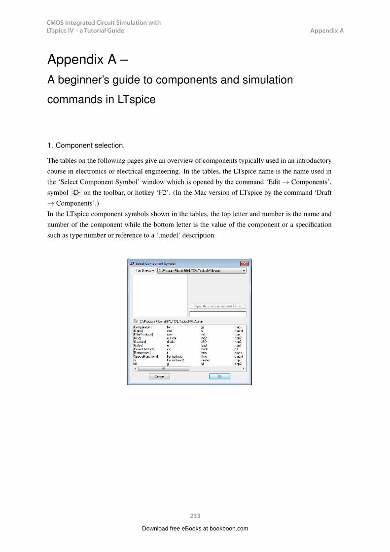
CMOS Integrated Circuit Simulation with LTspice IV – a Tutorial Guide
233
Appendix A
CMOS Integrated Circuit Simulation with LTspice IV Appendix A
Appendix A –A beginner’s guide to components and simulation
commands in LTspice
1. Component selection.
The tables on the following pages give an overview of components typically used in an introductorycourse in electronics or electrical engineering. In the tables, the LTspice name is the name used inthe ‘Select Component Symbol’ window which is opened by the command ‘Edit → Components’,symbol on the toolbar, or hotkey ‘F2’. (In the Mac version of LTspice by the command ‘Draft→ Components’.)In the LTspice component symbols shown in the tables, the top letter and number is the name andnumber of the component while the bottom letter is the value of the component or a specificationsuch as type number or reference to a ‘.model’ description.
233
Download free eBooks at bookboon.com
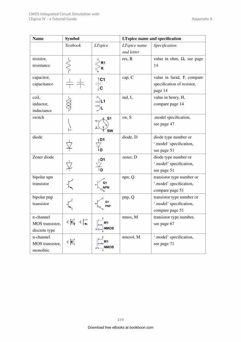
CMOS Integrated Circuit Simulation with LTspice IV – a Tutorial Guide
234
Appendix ACMOS Integrated Circuit Simulation with LTspice IV Appendix A
Name Symbol LTspice name and specificationTextbook LTspice LTspice name
and letterSpecification
resistor,resistance
res, R value in ohm, Ω, see page14
capacitor,capacitance
cap, C value in farad, F, comparespecification of resistor,page 14
coil,inductor,inductance
ind, L value in henry, H,compare page 14
switch sw, S .model specification,see page 47
diode diode, D diode type number or‘.model’ specification,see page 51
Zener diode zener, D diode type number or‘.model’ specification,see page 51
bipolar npntransistor
npn, Q transistor type number or‘.model’ specification,compare page 51
bipolar pnptransistor
pnp, Q transistor type number or‘.model’ specification,compare page 51
n-channelMOS transistor,discrete type
nmos, M transistor type number,see page 67
n-channelMOS transistor,monolitic
nmos4, M ‘.model’ specification,see page 71
234
Download free eBooks at bookboon.com
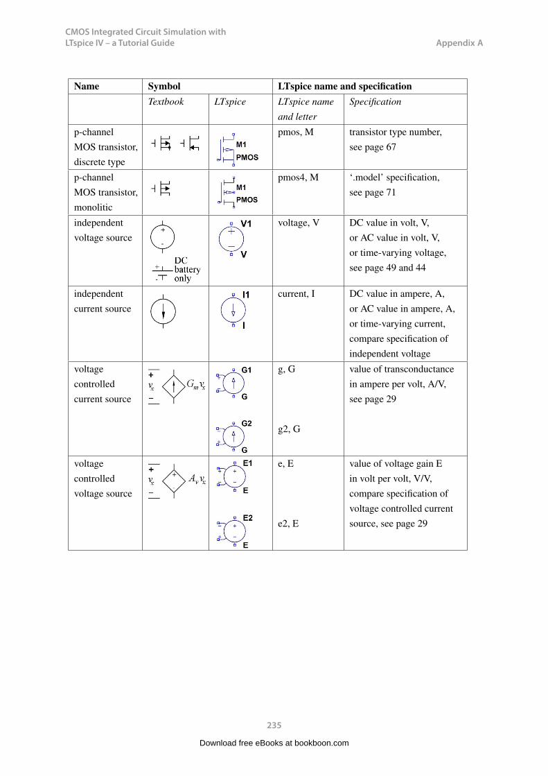
CMOS Integrated Circuit Simulation with LTspice IV – a Tutorial Guide
235
Appendix ACMOS Integrated Circuit Simulation with LTspice IV Appendix A
Name Symbol LTspice name and specificationTextbook LTspice LTspice name
and letterSpecification
p-channelMOS transistor,discrete type
pmos, M transistor type number,see page 67
p-channelMOS transistor,monolitic
pmos4, M ‘.model’ specification,see page 71
independentvoltage source
voltage, V DC value in volt, V,or AC value in volt, V,or time-varying voltage,see page 49 and 44
independentcurrent source
current, I DC value in ampere, A,or AC value in ampere, A,or time-varying current,compare specification ofindependent voltage
voltagecontrolledcurrent source
g, G
g2, G
value of transconductancein ampere per volt, A/V,see page 29
voltagecontrolledvoltage source
e, E
e2, E
value of voltage gain Ein volt per volt, V/V,compare specification ofvoltage controlled currentsource, see page 29
235
Download free eBooks at bookboon.com
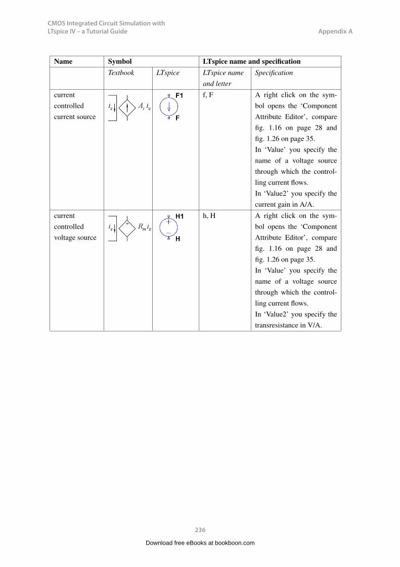
CMOS Integrated Circuit Simulation with LTspice IV – a Tutorial Guide
236
Appendix ACMOS Integrated Circuit Simulation with LTspice IV Appendix A
Name Symbol LTspice name and specificationTextbook LTspice LTspice name
and letterSpecification
currentcontrolledcurrent source
f, F A right click on the sym-bol opens the ‘ComponentAttribute Editor’, comparefig. 1.16 on page 28 andfig. 1.26 on page 35.In ‘Value’ you specify thename of a voltage sourcethrough which the control-ling current flows.In ‘Value2’ you specify thecurrent gain in A/A.
currentcontrolledvoltage source
h, H A right click on the sym-bol opens the ‘ComponentAttribute Editor’, comparefig. 1.16 on page 28 andfig. 1.26 on page 35.In ‘Value’ you specify thename of a voltage sourcethrough which the control-ling current flows.In ‘Value2’ you specify thetransresistance in V/A.
236
Download free eBooks at bookboon.com

CMOS Integrated Circuit Simulation with LTspice IV – a Tutorial Guide
237
Appendix ACMOS Integrated Circuit Simulation with LTspice IV Appendix A
Name Symbol LTspice name and specificationTextbook LTspice LTspice name
and letterSpecification
arbitrarycontrolledcurrent source
bi, B
bi2, B
mathematical expressionfor the current,compare fig. 1.18 on page29 and fig. 1.24 on page 33.
arbitrarycontrolledvoltage source
bv, B mathematical expressionfor the voltage, e.g.V=Av*V(Vin) whereAv is a voltage gain,or V=Rm*I(V1) whereRm is a transresistanceand I(V1) is the currentthrough a voltage sourceV1, compare fig. 1.24on page 33.
237
Download free eBooks at bookboon.com
Click on the ad to read moreClick on the ad to read moreClick on the ad to read moreClick on the ad to read moreClick on the ad to read moreClick on the ad to read moreClick on the ad to read moreClick on the ad to read moreClick on the ad to read moreClick on the ad to read moreClick on the ad to read moreClick on the ad to read moreClick on the ad to read moreClick on the ad to read moreClick on the ad to read moreClick on the ad to read moreClick on the ad to read moreClick on the ad to read moreClick on the ad to read moreClick on the ad to read moreClick on the ad to read moreClick on the ad to read moreClick on the ad to read moreClick on the ad to read moreClick on the ad to read moreClick on the ad to read moreClick on the ad to read moreClick on the ad to read moreClick on the ad to read moreClick on the ad to read moreClick on the ad to read moreClick on the ad to read moreClick on the ad to read moreClick on the ad to read moreClick on the ad to read moreClick on the ad to read moreClick on the ad to read moreClick on the ad to read moreClick on the ad to read moreClick on the ad to read moreClick on the ad to read moreClick on the ad to read moreClick on the ad to read moreClick on the ad to read moreClick on the ad to read moreClick on the ad to read moreClick on the ad to read moreClick on the ad to read moreClick on the ad to read moreClick on the ad to read moreClick on the ad to read moreClick on the ad to read moreClick on the ad to read moreClick on the ad to read moreClick on the ad to read moreClick on the ad to read moreClick on the ad to read moreClick on the ad to read moreClick on the ad to read moreClick on the ad to read moreClick on the ad to read moreClick on the ad to read moreClick on the ad to read moreClick on the ad to read moreClick on the ad to read moreClick on the ad to read moreClick on the ad to read moreClick on the ad to read moreClick on the ad to read moreClick on the ad to read moreClick on the ad to read moreClick on the ad to read moreClick on the ad to read moreClick on the ad to read moreClick on the ad to read moreClick on the ad to read moreClick on the ad to read moreClick on the ad to read moreClick on the ad to read moreClick on the ad to read moreClick on the ad to read moreClick on the ad to read more
© Deloitte & Touche LLP and affiliated entities.
360°thinking.
Discover the truth at www.deloitte.ca/careers
© Deloitte & Touche LLP and affiliated entities.
360°thinking.
Discover the truth at www.deloitte.ca/careers
© Deloitte & Touche LLP and affiliated entities.
360°thinking.
Discover the truth at www.deloitte.ca/careers © Deloitte & Touche LLP and affiliated entities.
360°thinking.
Discover the truth at www.deloitte.ca/careers

CMOS Integrated Circuit Simulation with LTspice IV – a Tutorial Guide
238
Appendix ACMOS Integrated Circuit Simulation with LTspice IV Appendix A
2. Overview of basic simulation commands.
The basic simulation commands used for simple circuits with DC voltages and currents, time varyingsignals and AC signals are ‘DC op pnt’, ‘DC sweep’, ‘Transient’, ‘DC Transfer’ and ‘AC Analysis’,compare page 16. In the Windows version of LTspice, these commands are inserted using ‘Simulate→ Edit Simulation Cmd’ which opens a window with help functions for each of the simulationcommands, see fig. 1.5 on page 18. In the Mac version, the window shown in fig. 1.5 is openedusing ‘Draft → SPICE Directives’ and a right click in the field for typing in the SPICE Directive.A very useful command in combination with the simulation commands is the LTspice directive ‘.stepparam’. By this command, parameter values can be swept over a specified range, so the commandis very useful for examining the properties of a circuit when component values are varied over aspecified range.
DC op pnt: This command computes DC currents and voltages in a circuit with capacitors treatedas open circuits and inductors as short circuits.Syntax: .opIn the Windows version of LTspice, the simulation results in an output file with all node voltagesand device currents in the circuit. In the Mac version, the simulation results in a plot window wherevoltages and currents can be displayed. Voltages and currents are selected by pointing at nodes orcomponents in the schematic, compare page 23. Alternatively, voltages and currents are available inthe Spice Error Log file which is shown by ‘View → Spice Error Log’ or hotkey ‘ L’.The simulation will run correctly only if DC voltages are defined in all nodes. If a node is connectedonly to capacitors or inputs to ideal voltage controlled sources, the node voltage is not defined andthe simulation may lead to erroneous results.
DC sweep: This command computes DC currents and voltages over a range of values for one, twoor three independent current sources or voltage sources.Syntax: .dc <srcnam> <Vstart> <Vstop> <Vincr>
where <srcname> is the name of an independent current source or voltage source, <Vstart> is thestart value and <Vstop> is the end value of the range of variation for the source. The step betweeneach simulation is specified by <Vincr>.The command is good for finding for instance the output voltage versus the input voltage for anamplifier.The simulation results in a plot window where voltages and currents can be displayed versus the(first) independent source which is stepped. Voltages and currents are selected by pointing at nodesor components in the schematic, see page 23.
238
Download free eBooks at bookboon.com

CMOS Integrated Circuit Simulation with LTspice IV – a Tutorial Guide
239
Appendix ACMOS Integrated Circuit Simulation with LTspice IV Appendix A
Transient: This command computes currents and voltages as a function of time in a circuit withone or more sources specified as time varying sources, see page 44.Syntax: .tran <Tstop>
where <Tstop> is the end time for the simulation. The command is good for analyzing for instancecharging or discharging of a capacitor or for finding time varying output signals versus time varyinginput signals in a circuit with amplifiers, capacitors and/or inductors.The command requires that the voltage is defined in all nodes at time t = 0. If a node is connectedonly to capacitors or inputs to ideal voltage controlled sources, the node voltage is not defined andit may be necessary to define the voltage by a ‘.ic’ command, see for instance fig. 2.13 on page 55.In a similar way, the initial current in an inductor can be defined by a ‘.ic’ command, see for instancefig. 2.15 on page 57.A ‘.ic’ command is also very useful when analyzing charging or discharging of capacitors or induc-tors, see for instance Example 2.5 on page 57.The simulation results in a plot window where voltages and current are shown versus time. Voltagesand currents are selected by pointing at nodes or components in the schematic, see page 23.For the transient simulation, a modifier [startup] may be specified after <Tstop>. This modifiercauses all DC sources in the circuit to ramp up linearly to the specified DC value during 20 µs.Do not use this modifier unless you are absolutely sure of what you are doing. Rather, use a ‘.ic’command as shown in Example 2.5 on page 57 or a time varying voltage or current, see page 44.
DC Transfer: This command computes the small signal input resistance, output resistance andtransfer function from an (independent) input source to an output at a frequency of 0 Hz.Syntax: .tf <V(vout)> <srcname>
where <V(vout)> is the voltage in the node labeled vout and <srcname> is the name of an inde-pendent voltage source or current source serving as the input signal.Alternatively, the output may be specified as I(<voltage source>) where <voltage source> isan independent voltage source through which the output current I flows.In the Windows version of LTspice, the simulation results in an output file showing the transfer func-tion, the input resistance and the output resistance, see fig. 1.21 on page 32. In the Mac version, thesimulation results in a plot window where the transfer function, the input resistance and the outputresistance can be selected using the command ‘Add Traces’.Just like the ‘.op’ command, the ‘.tf’ requires all DC node voltages to be defined.
AC Analysis: This command computes the small signal AC behavior of the circuit linearizedabout its DC operating point. This is used for finding the frequency response of a circuit, e.g. theBode plot of a gain function.
239
Download free eBooks at bookboon.com

CMOS Integrated Circuit Simulation with LTspice IV – a Tutorial Guide
240
Appendix ACMOS Integrated Circuit Simulation with LTspice IV Appendix A
Syntax: .ac <oct, dec, lin> <Nsteps> <StartFreq> <EndFreq>
where <StartFreq> and <EndFreq> denote the start and the end of the frequency range beingsimulated while <oct, dec, lin> and <Nsteps> determine the number of steps. Normally, youwould want a logarithmic frequency scale in which case you would use <oct> (the default) or <dec>and specify a suitable number of points per octave or decade of frequency.For this simulation, at least one independent source must be specified with an AC value, see forinstance fig. 2.7 on page 50.The simulation results in a plot window where voltages and current are shown versus frequency.Voltages and currents are selected by pointing at nodes or components in the schematic, see page23.
Parameter Sweep: Combined with the simulation commands above, the LTspice command ‘.stepparam’ may be used for analyzing the properties of a circuit when component values are varied overa specified range.Syntax: .step <Param> <Vstart> <Vstop> <Vincr>
where <Param> is the name of the parameter to be varied, <Vstart> is the start value of the param-eter, <Vstop> is the end value and <Vincr> is the step size of the parameter value between eachsimulation. When specifying a component value as a parameter, curly brackets are used to indicatethe name of the parameter, for instance R1, compare fig. 1.13 on page 26.Up to three parameters may be stepped in one simulation. The syntax shown above is the simplestform of the ‘.step’ command. Alternative ‘.step’ specifications are shown in the LTspice ‘help’ func-tion.A simulation with a parameter sweep results in a plot window. For a ‘.op’ or ‘.tf’ simulation, thex-axis is the (first) parameter being stepped. For ‘.dc’, ‘.tran’ and ‘.ac’ simulations, the x-axis is theindependent source, the time and the frequency, respectively, and separate traces are shown for eachvalue of the parameter which is stepped. Voltages and currents are selected by pointing at nodes orcomponents in the schematic, see page 23.
240
Download free eBooks at bookboon.com

CMOS Integrated Circuit Simulation with LTspice IV – a Tutorial Guide
241
Appendix B
Appendix B –BSIM transistor models for use in LTspice
The following pages give tables with BSIM transistor models adapted from (Carusone 2014) to becompatible with LTspice. The models have been modified to include the speed parameters SN andSP defined in Example 6.1 on page 180. For typical parameters, use SN = 0 and SP = 0. The filesinclude a command ‘.param SN=0 SP=0’ but it is inserted as a comment. To use only the typicalmodels, just un-comment this command by deleting the ‘*’ in the beginning of the command line.Alternatively, include a command specifying SN and SP in your schematic. The use of the speedparameters is described in Tutorial 6, Example 6.1 on page 180.
References
Carusone, TC., Johns, D. & Martin, K. 2014, Analog Integrated Circuit Design, Netlist and modelfiles. Retrieved from http://analogicdesign.com/students/netlists-models/
241Download free eBooks at bookboon.com
Click on the ad to read moreClick on the ad to read moreClick on the ad to read moreClick on the ad to read moreClick on the ad to read moreClick on the ad to read moreClick on the ad to read moreClick on the ad to read moreClick on the ad to read moreClick on the ad to read moreClick on the ad to read moreClick on the ad to read moreClick on the ad to read moreClick on the ad to read moreClick on the ad to read moreClick on the ad to read moreClick on the ad to read moreClick on the ad to read moreClick on the ad to read moreClick on the ad to read moreClick on the ad to read moreClick on the ad to read moreClick on the ad to read moreClick on the ad to read moreClick on the ad to read moreClick on the ad to read moreClick on the ad to read moreClick on the ad to read moreClick on the ad to read moreClick on the ad to read moreClick on the ad to read moreClick on the ad to read moreClick on the ad to read moreClick on the ad to read moreClick on the ad to read moreClick on the ad to read moreClick on the ad to read moreClick on the ad to read moreClick on the ad to read moreClick on the ad to read moreClick on the ad to read moreClick on the ad to read moreClick on the ad to read moreClick on the ad to read moreClick on the ad to read moreClick on the ad to read moreClick on the ad to read moreClick on the ad to read moreClick on the ad to read moreClick on the ad to read moreClick on the ad to read moreClick on the ad to read moreClick on the ad to read moreClick on the ad to read moreClick on the ad to read moreClick on the ad to read moreClick on the ad to read moreClick on the ad to read moreClick on the ad to read moreClick on the ad to read moreClick on the ad to read moreClick on the ad to read moreClick on the ad to read moreClick on the ad to read moreClick on the ad to read moreClick on the ad to read moreClick on the ad to read moreClick on the ad to read moreClick on the ad to read moreClick on the ad to read moreClick on the ad to read moreClick on the ad to read moreClick on the ad to read moreClick on the ad to read moreClick on the ad to read moreClick on the ad to read moreClick on the ad to read moreClick on the ad to read moreClick on the ad to read moreClick on the ad to read moreClick on the ad to read moreClick on the ad to read moreClick on the ad to read more
We will turn your CV into an opportunity of a lifetime
Do you like cars? Would you like to be a part of a successful brand?We will appreciate and reward both your enthusiasm and talent.Send us your CV. You will be surprised where it can take you.
Send us your CV onwww.employerforlife.com

CMOS Integrated Circuit Simulation with LTspice IV – a Tutorial Guide
242
Appendix BCMOS Integrated Circuit Simulation with LTspice IV Appendix B
Generic BSIM3 model for 0.35 µm CMOS process with speed parameters SN and SP to define process variations.To use without speed parameters and only with typical process parameters, un-comment the line *.PARAM SN=0 SP=0by deleting the *.
*BSIM3_035.lib*Speed parameters SN and SP*.PARAM SN=0 SP=0; Un-comment this command for use with only typical models.MODEL NMOS-BSIM NMOS LEVEL = 49+VERSION = 3.1 TNOM = 27 TOX = 7.8E-9/(1+SN/20)+XJ = 1E-07 NCH = 2.18E+17 VTH0 = 0.48-SN/10+K1 = 6.07E-01 K2 = 1.24E-03 K3 = 9.68E+01+K3B = -9.84E+00 W0 = 2.02E-05 NLX = 1.62E-07+DVT0W = 0 DVT1W = 0 DVT2W = 0+DVT0 = 2.87E+00 DVT1 = 5.86E-01 DVT2 = -1.26E-01+U0 = 360*(1+SN/20)**2 UA = -8.48E-10 UB = 2.27E-18+UC = 3.27E-11 VSAT = 1.87E+05 A0 = 1.22E+00+AGS = 2.06E-01 B0 = 9.60E-07 B1 = 4.95E-06+KETA = -1.67E-04 A1 = 0 A2 = 3.49E-01+RDSW = 8.18E+02 PRWG = 2.35E-02 PRWB = -8.12E-02+WR = 9.98E-01 WINT = 1.55E-07 LINT = 4.51E-10+DWG = -4.27E-09+DWB = 4.07E-09 VOFF = -4.14E-02 NFACTOR = 1.61E+00+CIT = 0 CDSC = 2.39E-04 CDSCD = 0.00E+00+CDSCB = 0 ETA0 = 1 ETAB = -1.99E-01+DSUB = 1 PCLM = 1.32E+00 PDIBLC1 = 2.42E-04+PDIBLC2 = 8.27E-03 PDIBLCB = -9.99E-04 DROUT = 9.72E-04+PSCBE1 = 7.24E+08 PSCBE2 = 9.96E-04 PVAG = 1.00E-02+DELTA = 1.01E-02 RSH = 3.33E+00 MOBMOD = 1+PRT = 0 UTE = -1.5 KT1 = -1.11E-01+KT1L = 0 KT2 = 2.22E-02 UA1 = 4.34E-09+UB1 = -7.56E-18 UC1 = -5.62E-11 AT = 3.31E+04+WL = 0 WLN = 9.95E-01 WW = 0+WWN = 1.00E+00 WWL = 0 LL = 0+LLN = 1 LW = 0 LWN = 1+LWL = 0 CAPMOD = 2 XPART = 0.5+CGDO = 2.76E-10 CGSO = 2.76E-10 CGBO = 1.00E-12+CJ = 9e-4/(1+SN/20) PB = 7.95E-01 MJ = 3.53E-01+CJSW = 2.8e-10/(1+SN/20) PBSW = 7.98E-01 MJSW = 1.73E-01+CJSWG = 1.81E-10 PBSWG = 7.96E-01 MJSWG = 1.74E-01+CF = 0 PVTH0 = -1.80E-02 PRDSW = -7.56E+01+PK2 = 4.48E-05 WKETA = -1.33E-03 LKETA = -8.91E-03
.MODEL PMOS-BSIM PMOS LEVEL = 49*Speed parameter SP+VERSION = 3.1 TNOM = 2.69E+01 TOX = 7.8E-9/(1+SP/20)+XJ = 1.00E-07 NCH = 8.44E+16 VTH0 = -0.6+SP/10+K1 = 4.82E-01 K2 = -2.13E-02 K3 = 8.27E+01+K3B = -5 W0 = 5.24E-06 NLX = 2.49E-07+DVT0W = 0.00E+00 DVT1W = 0 DVT2W = 0+DVT0 = 3.54E-01 DVT1 = 7.52E-01 DVT2 = -2.98E-01+U0 = 150*(1+SP/20)**2 UA = 1E-10 UB = 1.75E-18+UC = -2.27E-11 VSAT = 2.01E+05 A0 = 1.04E+00+AGS = 2.90E-01 B0 = 1.94E-06 B1 = 5.01E-06+KETA = -3.85E-03 A1 = 4.20E-03 A2 = 1.00E+00+RDSW = 4000 PRWG = -9.54E-02 PRWB = -1.92E-03+WR = 1 WINT = 1.47E-07 LINT = 1.04E-10+DWG = -1.09E-08+DWB = 1.14E-08 VOFF = -1.29E-01 NFACTOR = 2.01E+00+CIT = 0 CDSC = 2.40E-04 CDSCD = 0+CDSCB = 0 ETA0 = 4.07E-02 ETAB = 6.84E-03+DSUB = 3.21E-01 PCLM = 5.96E+00 PDIBLC1 = 2.89E-03+PDIBLC2 = -1.45E-06 PDIBLCB = -1E-03 DROUT = 9.93E-04+PSCBE1 = 7.88E+10 PSCBE2 = 5E-10 PVAG = 15+DELTA = 9.96E-03 RSH = 2.6 MOBMOD = 1+PRT = 0 UTE = -1.5 KT1 = -1.09E-01+KT1L = 0 KT2 = 2.19E-02 UA1 = 4.34E-09+UB1 = -7.62E-18 UC1 = -5.63E-11 AT = 3.28E+04+WL = 0 WLN = 1 WW = 0+WWN = 1.00E+00 WWL = 0 LL = 0+LLN = 1 LW = 0 LWN = 1+LWL = 0 CAPMOD = 2.01E+00 XPART = 0.5+CGDO = 2.10E-10 CGSO = 2.12E-10 CGBO = 1.00E-12+CJ = 14e-4/(1+SP/20) PB = 9.83E-01 MJ = 5.79E-01+CJSW = 3.2e-10/(1+SP/20) PBSW = 9.92E-01 MJSW = 3.60E-01+CJSWG = 4.41E-11 PBSWG = 9.85E-01 MJSWG = 3.58E-01+CF = 0 PVTH0 = 2.58E-02 PRDSW = -3.98E+01+PK2 = 2.02E-03 WKETA = 2.72E-03 LKETA = -7.14E-03
242
Download free eBooks at bookboon.com

CMOS Integrated Circuit Simulation with LTspice IV – a Tutorial Guide
243
Appendix BCMOS Integrated Circuit Simulation with LTspice IV Appendix B
Generic BSIM3 model for 0.18 µm CMOS process with speed parameters SN and SP to define process variations.To use without speed parameters and only with typical process parameters, un-comment the line *.PARAM SN=0 SP=0by deleting the *.
*BSIM3_018.lib*Speed parameters SN and SP*.PARAM SN=0 SP=0; Un-comment this command for use with only typical models.MODEL NMOS-BSIM NMOS + VERSION = 3+ LEVEL = 49 NOIMOD = 1 TNOM = 2.70E+01+ TOX = 4.1E-9/(1+SN/20) XJ = 1.00E-07 NCH = 2.33E+17+ VTH0 = 0.36-SN/10 K1 = 5.84E-01 K2 = 4.14E-03+ K3 = 1.01E-03 K3B = 2.20E+00 W0 = 1.00E-07+ NLX = 1.81E-07DVT0W = 0.00E+00 DVT1W = 0.00E+00+ DVT2W = 0.00E+00 DVT0 = 1.73E+00 DVT1 = 4.38E-01+ DVT2 = -3.70E-04 U0 =260*(1+SN/20)**2 UA = -1.38E-09+ UB = 2.26E-18 UC = 5.46E-11 VSAT = 1.03E+05+ A0 = 1.92E+00 AGS = 4.20E-01 B0 = -1.52E-09+ B1 = -9.92E-08 KETA = -7.16E-03 A1 = 6.61E-04+ A2 = 8.89E-01 RDSW = 1.12E+02 PRWG = 4.92E-01+ PRWB = -2.02E-01 WR = 1.00E+00 + WINT = 7.12E-09 LINT = 1.12E-08+ DWG = -3.82E-09 DWB = 8.63E-09 VOFF = -8.82E-02+ NFACTOR = 2.30E+00 CIT = 0.00E+00 CDSC = 2.40E-04+ CDSCD = 0.00E+00 CDSCB = 0.00E+00 ETA0 = 3.13E-03+ ETAB = 1.00E+00 DSUB = 2.25E-02 PCLM = 7.20E-01+ PDIBLC1 = 2.15E-01 PDIBLC2 = 2.23E-03 PDIBLCB = 1.00E-01+ DROUT = 8.01E-01 PSCBE1 = 5.44E+08 PSCBE2 = 1.00E-03+ PVAG = 1.00E-12 DELTA = 1.00E-02 RSH = 6.78E+00+ MOBMOD = 1.00E+00 PRT = 0.00E+00 UTE = -1.50E+00+ KT1 = -1.10E-01 KT1L = 0.00E+00 KT2 = 2.19E-02+ UA1 = 4.28E-09UB1 = -7.62E-18 UC1 = -5.57E-11+ AT = 3.30E+04 WL = 0.00E+00 WLN = 1.00E+00+ WW = 0.00E+00 WWN = 1.00E+00 WWL = 0.00E+00+ LL = 0.00E+00 LLN = 1.00E+00 LW = 0.00E+00+ LWN = 1.00E+00 LWL = 0.00E+00 CAPMOD = 2.00E+00+ XPART = 5.00E-01 CGDO = 6.98E-10 CGSO = 7.03E-10+ CGBO = 1.00E-12 CJ = 9.8e-4/(1+SN/20) PB = 7.34E-01+ MJ = 3.63E-01 CJSW = 2.4e-10/(1+SN/20) PBSW = 4.71E-01+ MJSW = 1.00E-01 CJSWG = 3.29E-10 PBSWG = 4.66E-01+ MJSWG = 1.00E-01 CF = 0.00E+00 PVTH0 = -7.16E-04+ PRDSW = -6.66E-01 PK2 = 5.92E-04 WKETA = 2.14E-04+ LKETA = -1.51E-02 PU0 = 3.36E+00 PUA = -1.31E-11+ PUB = 0.00E+00 PVSAT = 1.25E+03 PETA0 = 1.00E-04+ PKETA = 6.45E-04 KF = 4.46E-29
.MODEL PMOS-BSIM PMOS + VERSION = 3.1 + LEVEL = 49 NOIMOD = 1 + TNOM = 2.70E+01 TOX = 4.1E-9/(1+SP/20) XJ = 1.00E-07+ NCH = 4.12E+17 VTH0 = -0.39+SP/10 K1 = 5.50E-01+ K2 = 3.50E-02 K3 = 0.00E+00 K3B = 1.20E+01+ W0 = 1.00E-06 NLX = 1.25E-07 DVT0W = 0.00E+00+ DVT1W = 0.00E+00 DVT2W = 0.00E+00 DVT0 = 5.53E-01+ DVT1 = 2.46E-01 DVT2 = 1.00E-01 U0 = 110*(1+SP/20)**2+ UA = 1.44E-09 UB = 2.29E-21 UC = -1.00E-10+ VSAT = 1.95E+05 A0 = 1.72E+00 AGS = 3.80E-01+ B0 = 5.87E-07 B1 = 1.44E-06 KETA = 2.21E-02+ A1 = 4.66E-01 A2 = 3.00E-01 RDSW = 3.11E+02+ PRWG = 5.00E-01 PRWB = 1.64E-02 WR = 1.00E+00+ WINT = 0.00E+00 LINT = 2.00E-08+ DWG = -3.49E-08 DWB = 1.22E-09+ VOFF = -9.80E-02 NFACTOR = 2.00E+00 CIT = 0.00E+00+ CDSC = 2.40E-04 CDSCD = 0.00E+00 CDSCB = 0.00E+00+ ETA0 = 1.12E-03 ETAB = -4.79E-04 DSUB = 1.60E-03+ PCLM = 1.50E+00 PDIBLC1 = 3.00E-02 PDIBLC2 = -1.01E-05+ PDIBLCB = 1.00E-01 DROUT = 1.56E-03 PSCBE1 = 4.91E+09+ PSCBE2 = 1.64E-09 PVAG = 3.48E+00 DELTA = 1.00E-02+ RSH = 7.69E+00 MOBMOD = 1.00E+00 PRT = 0.00E+00+ UTE = -1.49E+00 KT1 = -1.09E-01KT1L = 0.00E+00+ KT2 = 2.18E-02 UA1 = 4.27E-09 UB1 = -7.68E-18+ UC1 = -5.57E-11 AT = 3.31E+04 WL = 0.00E+00+ WLN = 1.00E+00 WW = 0.00E+00 WWN = 1.00E+00+ WWL = 0.00E+00 LL = 0.00E+00 LLN = 1.00E+00+ LW = 0.00E+00 LWN = 1.00E+00 LWL = 0.00E+00+ CAPMOD = 2.00E+00 XPART = 5.00E-01 CGDO = 6.88E-10+ CGSO = 6.85E-10 CGBO = 1.00E-12 CJ = 1.2e-3/(1+SP/20)+ PB = 8.70E-01 MJ = 4.20E-01 CJSW = 2.4e-10/(1+SP/20)+ PBSW = 8.00E-01 MJSW = 3.57E-01 CJSWG = 4.24E-10+ PBSWG = 8.00E-01 MJSWG = 3.56E-01 CF = 0.00E+00+ PVTH0 = 3.53E-03 PRDSW = 1.02E+01 PK2 = 3.35E-03+ WKETA = 3.52E-02 LKETA = -2.06E-03 PU0 = -2.19E+00+ PUA = -7.63E-11 PUB = 9.91E-22 PVSAT = 5.00E+01+ PKETA = -6.41E-03 KF = 1.29E-29 PETA0 = 7.31E-05
243
Download free eBooks at bookboon.com
Click on the ad to read moreClick on the ad to read moreClick on the ad to read moreClick on the ad to read moreClick on the ad to read moreClick on the ad to read moreClick on the ad to read moreClick on the ad to read moreClick on the ad to read moreClick on the ad to read moreClick on the ad to read moreClick on the ad to read moreClick on the ad to read moreClick on the ad to read moreClick on the ad to read moreClick on the ad to read moreClick on the ad to read moreClick on the ad to read moreClick on the ad to read moreClick on the ad to read moreClick on the ad to read moreClick on the ad to read moreClick on the ad to read moreClick on the ad to read moreClick on the ad to read moreClick on the ad to read moreClick on the ad to read moreClick on the ad to read moreClick on the ad to read moreClick on the ad to read moreClick on the ad to read moreClick on the ad to read moreClick on the ad to read moreClick on the ad to read moreClick on the ad to read moreClick on the ad to read moreClick on the ad to read moreClick on the ad to read moreClick on the ad to read moreClick on the ad to read moreClick on the ad to read moreClick on the ad to read moreClick on the ad to read moreClick on the ad to read moreClick on the ad to read moreClick on the ad to read moreClick on the ad to read moreClick on the ad to read moreClick on the ad to read moreClick on the ad to read moreClick on the ad to read moreClick on the ad to read moreClick on the ad to read moreClick on the ad to read moreClick on the ad to read moreClick on the ad to read moreClick on the ad to read moreClick on the ad to read moreClick on the ad to read moreClick on the ad to read moreClick on the ad to read moreClick on the ad to read moreClick on the ad to read moreClick on the ad to read moreClick on the ad to read moreClick on the ad to read moreClick on the ad to read moreClick on the ad to read moreClick on the ad to read moreClick on the ad to read moreClick on the ad to read moreClick on the ad to read moreClick on the ad to read moreClick on the ad to read moreClick on the ad to read moreClick on the ad to read moreClick on the ad to read moreClick on the ad to read moreClick on the ad to read moreClick on the ad to read moreClick on the ad to read moreClick on the ad to read moreClick on the ad to read moreClick on the ad to read more
Maersk.com/Mitas
e Graduate Programme for Engineers and Geoscientists
Month 16I was a construction
supervisor in the North Sea
advising and helping foremen
solve problems
I was a
hes
Real work International opportunities
ree work placementsal Internationaorree wo
I wanted real responsibili I joined MITAS because
www.discovermitas.com
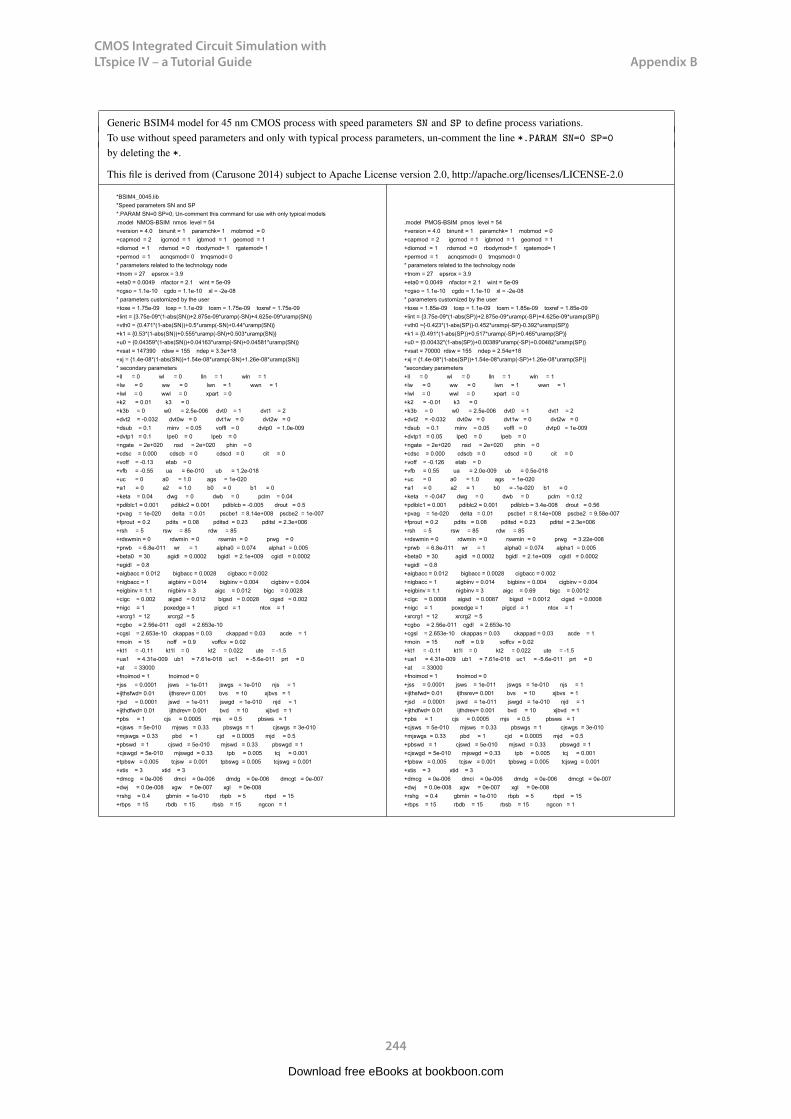
CMOS Integrated Circuit Simulation with LTspice IV – a Tutorial Guide
244
Appendix BCMOS Integrated Circuit Simulation with LTspice IV Appendix B
Generic BSIM4 model for 45 nm CMOS process with speed parameters SN and SP to define process variations.To use without speed parameters and only with typical process parameters, un-comment the line *.PARAM SN=0 SP=0by deleting the *.
This file is derived from (Carusone 2014) subject to Apache License version 2.0, http://apache.org/licenses/LICENSE-2.0
*BSIM4_0045.lib*Speed parameters SN and SP*.PARAM SN=0 SP=0; Un-comment this command for use with only typical models.model NMOS-BSIM nmos level = 54+version = 4.0 binunit = 1 paramchk= 1 mobmod = 0+capmod = 2 igcmod = 1 igbmod = 1 geomod = 1+diomod = 1 rdsmod = 0 rbodymod= 1 rgatemod= 1+permod = 1 acnqsmod= 0 trnqsmod= 0* parameters related to the technology node+tnom = 27 epsrox = 3.9+eta0 = 0.0049 nfactor = 2.1 wint = 5e-09+cgso = 1.1e-10 cgdo = 1.1e-10 xl = -2e-08* parameters customized by the user+toxe = 1.75e-09 toxp = 1.1e-09 toxm = 1.75e-09 toxref = 1.75e-09+lint = 3.75e-09*(1-abs(SN))+2.875e-09*uramp(-SN)+4.625e-09*uramp(SN)+vth0 = 0.471*(1-abs(SN))+0.5*uramp(-SN)+0.44*uramp(SN)+k1 = 0.53*(1-abs(SN))+0.555*uramp(-SN)+0.503*uramp(SN) +u0 = 0.04359*(1-abs(SN))+0.04163*uramp(-SN)+0.04581*uramp(SN) +vsat = 147390 rdsw = 155 ndep = 3.3e+18 +xj = 1.4e-08*(1-abs(SN))+1.54e-08*uramp(-SN)+1.26e-08*uramp(SN)* secondary parameters+ll = 0 wl = 0 lln = 1 wln = 1 +lw = 0 ww = 0 lwn = 1 wwn = 1 +lwl = 0 wwl = 0 xpart = 0 +k2 = 0.01 k3 = 0 +k3b = 0 w0 = 2.5e-006 dvt0 = 1 dvt1 = 2 +dvt2 = -0.032 dvt0w = 0 dvt1w = 0 dvt2w = 0 +dsub = 0.1 minv = 0.05 voffl = 0 dvtp0 = 1.0e-009 +dvtp1 = 0.1 lpe0 = 0 lpeb = 0 +ngate = 2e+020 nsd = 2e+020 phin = 0 +cdsc = 0.000 cdscb = 0 cdscd = 0 cit = 0 +voff = -0.13 etab = 0 +vfb = -0.55 ua = 6e-010 ub = 1.2e-018 +uc = 0 a0 = 1.0 ags = 1e-020 +a1 = 0 a2 = 1.0 b0 = 0 b1 = 0 +keta = 0.04 dwg = 0 dwb = 0 pclm = 0.04 +pdiblc1 = 0.001 pdiblc2 = 0.001 pdiblcb = -0.005 drout = 0.5 +pvag = 1e-020 delta = 0.01 pscbe1 = 8.14e+008 pscbe2 = 1e-007 +fprout = 0.2 pdits = 0.08 pditsd = 0.23 pditsl = 2.3e+006 +rsh = 5 rsw = 85 rdw = 85 +rdswmin = 0 rdwmin = 0 rswmin = 0 prwg = 0 +prwb = 6.8e-011 wr = 1 alpha0 = 0.074 alpha1 = 0.005 +beta0 = 30 agidl = 0.0002 bgidl = 2.1e+009 cgidl = 0.0002 +egidl = 0.8 +aigbacc = 0.012 bigbacc = 0.0028 cigbacc = 0.002 +nigbacc = 1 aigbinv = 0.014 bigbinv = 0.004 cigbinv = 0.004 +eigbinv = 1.1 nigbinv = 3 aigc = 0.012 bigc = 0.0028 +cigc = 0.002 aigsd = 0.012 bigsd = 0.0028 cigsd = 0.002 +nigc = 1 poxedge = 1 pigcd = 1 ntox = 1 +xrcrg1 = 12 xrcrg2 = 5 +cgbo = 2.56e-011 cgdl = 2.653e-10 +cgsl = 2.653e-10 ckappas = 0.03 ckappad = 0.03 acde = 1 +moin = 15 noff = 0.9 voffcv = 0.02 +kt1 = -0.11 kt1l = 0 kt2 = 0.022 ute = -1.5 +ua1 = 4.31e-009 ub1 = 7.61e-018 uc1 = -5.6e-011 prt = 0 +at = 33000 +fnoimod = 1 tnoimod = 0 +jss = 0.0001 jsws = 1e-011 jswgs = 1e-010 njs = 1 +ijthsfwd= 0.01 ijthsrev= 0.001 bvs = 10 xjbvs = 1 +jsd = 0.0001 jswd = 1e-011 jswgd = 1e-010 njd = 1 +ijthdfwd= 0.01 ijthdrev= 0.001 bvd = 10 xjbvd = 1 +pbs = 1 cjs = 0.0005 mjs = 0.5 pbsws = 1 +cjsws = 5e-010 mjsws = 0.33 pbswgs = 1 cjswgs = 3e-010 +mjswgs = 0.33 pbd = 1 cjd = 0.0005 mjd = 0.5 +pbswd = 1 cjswd = 5e-010 mjswd = 0.33 pbswgd = 1 +cjswgd = 5e-010 mjswgd = 0.33 tpb = 0.005 tcj = 0.001 +tpbsw = 0.005 tcjsw = 0.001 tpbswg = 0.005 tcjswg = 0.001 +xtis = 3 xtid = 3 +dmcg = 0e-006 dmci = 0e-006 dmdg = 0e-006 dmcgt = 0e-007 +dwj = 0.0e-008 xgw = 0e-007 xgl = 0e-008 +rshg = 0.4 gbmin = 1e-010 rbpb = 5 rbpd = 15 +rbps = 15 rbdb = 15 rbsb = 15 ngcon = 1
.model PMOS-BSIM pmos level = 54+version = 4.0 binunit = 1 paramchk= 1 mobmod = 0+capmod = 2 igcmod = 1 igbmod = 1 geomod = 1+diomod = 1 rdsmod = 0 rbodymod= 1 rgatemod= 1+permod = 1 acnqsmod= 0 trnqsmod= 0* parameters related to the technology node+tnom = 27 epsrox = 3.9+eta0 = 0.0049 nfactor = 2.1 wint = 5e-09+cgso = 1.1e-10 cgdo = 1.1e-10 xl = -2e-08* parameters customized by the user+toxe = 1.85e-09 toxp = 1.1e-09 toxm = 1.85e-09 toxref = 1.85e-09+lint = 3.75e-09*(1-abs(SP))+2.875e-09*uramp(-SP)+4.625e-09*uramp(SP) +vth0 =-0.423*(1-abs(SP))-0.452*uramp(-SP)-0.392*uramp(SP) +k1 = 0.491*(1-abs(SP))+0.517*uramp(-SP)+0.465*uramp(SP) +u0 = 0.00432*(1-abs(SP))+0.00389*uramp(-SP)+0.00482*uramp(SP) +vsat = 70000 rdsw = 155 ndep = 2.54e+18 +xj = 1.4e-08*(1-abs(SP))+1.54e-08*uramp(-SP)+1.26e-08*uramp(SP) *secondary parameters+ll = 0 wl = 0 lln = 1 wln = 1 +lw = 0 ww = 0 lwn = 1 wwn = 1 +lwl = 0 wwl = 0 xpart = 0 +k2 = -0.01 k3 = 0 +k3b = 0 w0 = 2.5e-006 dvt0 = 1 dvt1 = 2 +dvt2 = -0.032 dvt0w = 0 dvt1w = 0 dvt2w = 0 +dsub = 0.1 minv = 0.05 voffl = 0 dvtp0 = 1e-009 +dvtp1 = 0.05 lpe0 = 0 lpeb = 0 +ngate = 2e+020 nsd = 2e+020 phin = 0 +cdsc = 0.000 cdscb = 0 cdscd = 0 cit = 0 +voff = -0.126 etab = 0 +vfb = 0.55 ua = 2.0e-009 ub = 0.5e-018 +uc = 0 a0 = 1.0 ags = 1e-020 +a1 = 0 a2 = 1 b0 = -1e-020 b1 = 0 +keta = -0.047 dwg = 0 dwb = 0 pclm = 0.12 +pdiblc1 = 0.001 pdiblc2 = 0.001 pdiblcb = 3.4e-008 drout = 0.56 +pvag = 1e-020 delta = 0.01 pscbe1 = 8.14e+008 pscbe2 = 9.58e-007+fprout = 0.2 pdits = 0.08 pditsd = 0.23 pditsl = 2.3e+006 +rsh = 5 rsw = 85 rdw = 85 +rdswmin = 0 rdwmin = 0 rswmin = 0 prwg = 3.22e-008+prwb = 6.8e-011 wr = 1 alpha0 = 0.074 alpha1 = 0.005 +beta0 = 30 agidl = 0.0002 bgidl = 2.1e+009 cgidl = 0.0002 +egidl = 0.8 +aigbacc = 0.012 bigbacc = 0.0028 cigbacc = 0.002 +nigbacc = 1 aigbinv = 0.014 bigbinv = 0.004 cigbinv = 0.004 +eigbinv = 1.1 nigbinv = 3 aigc = 0.69 bigc = 0.0012 +cigc = 0.0008 aigsd = 0.0087 bigsd = 0.0012 cigsd = 0.0008 +nigc = 1 poxedge = 1 pigcd = 1 ntox = 1 +xrcrg1 = 12 xrcrg2 = 5 +cgbo = 2.56e-011 cgdl = 2.653e-10+cgsl = 2.653e-10 ckappas = 0.03 ckappad = 0.03 acde = 1+moin = 15 noff = 0.9 voffcv = 0.02+kt1 = -0.11 kt1l = 0 kt2 = 0.022 ute = -1.5 +ua1 = 4.31e-009 ub1 = 7.61e-018 uc1 = -5.6e-011 prt = 0 +at = 33000 +fnoimod = 1 tnoimod = 0 +jss = 0.0001 jsws = 1e-011 jswgs = 1e-010 njs = 1 +ijthsfwd= 0.01 ijthsrev= 0.001 bvs = 10 xjbvs = 1 +jsd = 0.0001 jswd = 1e-011 jswgd = 1e-010 njd = 1 +ijthdfwd= 0.01 ijthdrev= 0.001 bvd = 10 xjbvd = 1 +pbs = 1 cjs = 0.0005 mjs = 0.5 pbsws = 1 +cjsws = 5e-010 mjsws = 0.33 pbswgs = 1 cjswgs = 3e-010 +mjswgs = 0.33 pbd = 1 cjd = 0.0005 mjd = 0.5 +pbswd = 1 cjswd = 5e-010 mjswd = 0.33 pbswgd = 1 +cjswgd = 5e-010 mjswgd = 0.33 tpb = 0.005 tcj = 0.001 +tpbsw = 0.005 tcjsw = 0.001 tpbswg = 0.005 tcjswg = 0.001 +xtis = 3 xtid = 3 +dmcg = 0e-006 dmci = 0e-006 dmdg = 0e-006 dmcgt = 0e-007 +dwj = 0.0e-008 xgw = 0e-007 xgl = 0e-008 +rshg = 0.4 gbmin = 1e-010 rbpb = 5 rbpd = 15 +rbps = 15 rbdb = 15 rbsb = 15 ngcon = 1
244
Download free eBooks at bookboon.com
CMOS Integrated Circuit Simulation with LTspice IV – a Tutorial Guide
245
Index
Index
.ac, 17, 48, 239
.dc, 17, 22, 238
.end, 213
.ends, 215
.global, 168, 174
.ic, 54, 57, 239
.inc, .include, 77
.meas, .measure, 60, 189
.model, 46, 50, 67, 75, 241
.noise, 17, 127, 135
.op, 17, 238
.param, 27
.step, 25, 183, 240
.subckt, 215
.temp, 186
.tf, 17, 32, 239
.tran, 17, 44, 239
Active load, 109Amplifier
cascode, 124common drain, 114common gate, 121common source, 103current, 32, 236differential, 126inverting, 27, 103operational, 147transconductance, 27, 235transresistance, 34, 236voltage, 235
Annotatingon schematics, 20, 79on waveform plots, 26
Bipolar transistor, 234Bode plot, 64Bus wire, 172
Capacitor, 44Capacitor charging, 44, 57Capacitor discharging, 44, 57Closed loop gain, 162, 198Colour preferences, 21, 24Common mode rejection ratio, CMRR, 132Component Attribute Editor, 28Ctrl-L, 73, 95, 190Current conveyor, 215Current source
arbitrary behavioral, 29arbitrary controlled, 237current controlled, 32, 236independent, 20, 235voltage controlled, 28, 235
Cursor in plot window, 95Cursor in plot windows, 24, 46, 81
DC feedback path, 197Diode, 50Drawing a schematic, 13
Error log file, 11, 19, 73, 95, 190, 238
Download free eBooks at bookboon.com

CMOS Integrated Circuit Simulation with LTspice IV – a Tutorial Guide
246
Index
Exportingschematics, 16waveforms, 24
Font size, 21
Generic filter functions, 165Ground, 15
Hierarchical design, 147
Inductor, 55Inductor demagnetization, 55, 59Inductor magnetization, 55, 59
Label Net, 15Logic gates, 168Loop gain, 162, 197
Mac computer, 10MOS transistor, 67
Netlist, 19, 211export, 221import, 211
Noise, 135Norton equivalent, 19
Power supply rejection ratio, PSRR, 132Process corners, 179Process, voltage and temperature variations,
PVT, 180
RC network, 43Rectifier, 50Resistor, 13
Download free eBooks at bookboon.com
Click on the ad to read moreClick on the ad to read moreClick on the ad to read moreClick on the ad to read moreClick on the ad to read moreClick on the ad to read moreClick on the ad to read moreClick on the ad to read moreClick on the ad to read moreClick on the ad to read moreClick on the ad to read moreClick on the ad to read moreClick on the ad to read moreClick on the ad to read moreClick on the ad to read moreClick on the ad to read moreClick on the ad to read moreClick on the ad to read moreClick on the ad to read moreClick on the ad to read moreClick on the ad to read moreClick on the ad to read moreClick on the ad to read moreClick on the ad to read moreClick on the ad to read moreClick on the ad to read moreClick on the ad to read moreClick on the ad to read moreClick on the ad to read moreClick on the ad to read moreClick on the ad to read moreClick on the ad to read moreClick on the ad to read moreClick on the ad to read moreClick on the ad to read moreClick on the ad to read moreClick on the ad to read moreClick on the ad to read moreClick on the ad to read moreClick on the ad to read moreClick on the ad to read moreClick on the ad to read moreClick on the ad to read moreClick on the ad to read moreClick on the ad to read moreClick on the ad to read moreClick on the ad to read moreClick on the ad to read moreClick on the ad to read moreClick on the ad to read moreClick on the ad to read moreClick on the ad to read moreClick on the ad to read moreClick on the ad to read moreClick on the ad to read moreClick on the ad to read moreClick on the ad to read moreClick on the ad to read moreClick on the ad to read moreClick on the ad to read moreClick on the ad to read moreClick on the ad to read moreClick on the ad to read moreClick on the ad to read moreClick on the ad to read moreClick on the ad to read moreClick on the ad to read moreClick on the ad to read moreClick on the ad to read moreClick on the ad to read moreClick on the ad to read moreClick on the ad to read moreClick on the ad to read moreClick on the ad to read moreClick on the ad to read moreClick on the ad to read moreClick on the ad to read moreClick on the ad to read moreClick on the ad to read moreClick on the ad to read moreClick on the ad to read moreClick on the ad to read moreClick on the ad to read moreClick on the ad to read moreClick on the ad to read more
CMOS Integrated Circuit Simulation with LTspice IV – a Tutorial Guide
247
Index
SimulationAC Analysis, 16, 48, 239DC op pnt, 16, 238DC sweep, 16, 22, 238DC Transfer, 16, 32, 239Monte Carlo, 198Noise, 16, 127, 135Transient, 16, 44, 239
Slew rate, 135Small signal output conductance, 72, 85, 90Small signal transconductance, 72, 82, 90Small signal transistor parameters, 72, 73,
86, 90Source follower, 114Speed parameter, 180Subcircuit, 147, 215Subcircuit device currents, 152, 218Subcircuit node voltages, 152, 218Sweeping a component value, 25Sweeping a DC current, 22
Sweeping a DC voltage, 22Switch, 46Symbol editor, 30, 150, 215
Thévenin equivalent, 19Transistor model
BSIM, 69, 75, 241Shichman-Hodges, 69
Two stage opamp, 147
Voltage sourcearbitrary controlled, 237current controlled, 236independent, 15, 235voltage controlled, 235
Waveform viewer, 23Windows computer, 10
Zener diode, 51, 234
Download free eBooks at bookboon.com


