Embed Size (px)
Citation preview

THE MINISTRY OF SCIENCE AND HIGHER EDUCATION OF THE RUSSIAN FEDERATION
Peter the Great St. Petersburg
Polytechnic University
2021
Computing, Telecommunications
and Control
Vol. 14, no. 22021
MEMS Technologies – Theory and Practice
COMPUTING, TELECOMMUNICATIONS AND CONTROL
EDITORIAL COUNCIL
Head of the editorial councilProf. Dr. Rafael M. Yusupov (corresponding member of the Russian Academy of Sciences)
Members:Prof. Dr. Sergey M. Abramov (corresponding member of the Russian Academy of Sciences),Prof. Dr. Dmitry G. Arseniev,Prof. Dr. Vladimir V. Voevodin (corresponding member of the Russian Academy of Sciences),Prof. Dr. Vladimir S. Zaborovsky,Prof. Dr. Vladimir N. Kozlov,Prof. Dr. Alexandr E. Fotiadi,Prof. Dr. Igor G. Chernorutsky.
EDITORIAL BOARD
Editor-in-chiefProf. Dr. Alexander S. Korotkov, Peter the Great St. Petersburg Polytechnic University, Russia;
Members:Assoc. Prof. Dr. Vladimir M. Itsykson, Peter the Great St. Petersburg Polytechnic University, Russia;Prof. Dr. Philippe Ferrari, Head of the RF and Millimeter-Wave Lab IMEP-LAHC Microelectronics, Electromagnetism and Photonic Institute, Grenoble Alpes University, France;Prof. Dr. Yevgeni Koucheryavy, Tampere University of Technology, Finland.Prof. Dr. Wolfgang Krautschneider, Head of Nanoelectronics Institute, Hamburg University of Technology, Germany;Prof. Dr. Fa-Long Luo, Affiliate Full Professor University of Washington, USA, Chief Scientist Micron Technology, Inc., Milpitas, USA, Chairman IEEE SPS Industry DSP Technology Standing Committee;Prof. Dr. Sergey B. Makarov, Peter the Great St. Petersburg Polytechnic University, Russia;Prof. Dr. Emil Novakov, IMEP-LAHC Microelectronics, Electromagnetism and Photonic Institute, Grenoble, France;Prof. Dr. Nikolay N. Prokopenko, Don State Technical University, Rostov-on-Don, Russia;Prof. Dr. Mikhail G. Putrya, National Research University of Electronic Technology, Moscow, Russia;Sen. Assoc. Prof. Dr. Evgeny Pyshkin, School of Computer Science and Engineering, University of Aizu, Japan;Prof. Dr. Viacheslav P. Shkodyrev, Peter the Great St. Petersburg Polytechnic University, Russia;Prof. Dr. Peter V. Trifonov, Peter the Great St. Petersburg Polytechnic University, Russia;Prof. Dr. Igor A. Tsikin, Professor, Peter the Great St. Petersburg Polytechnic University, Russia;Prof. Dr. Sergey M. Ustinov, Peter the Great St. Petersburg Polytechnic University, Russia;Prof. Dr. Lev V. Utkin, Peter the Great St. Petersburg Polytechnic University, Russia.
The journal is included in the List of Leading PeerReviewed Scientific Journals and other editions to publish major findings of PhD theses for the research degrees of Doctor of Sciences and Candidate of Sciences.
The journal is indexed by Ulrich’s Periodicals Directory, Google Scholar, EBSCO, ProQuest, Index Copernicus, VINITI RAS Abstract Journal (Referativnyi Zhurnal), VINITI RAS Scientific and Technical Literature Collection, Russian Science Citation Index (RSCI) database © Scientific Electronic Library and Math-Net.ru databases.
The journal is registered with the Federal Service for Supervision in the Sphere of Telecom, Information Technologies and Mass Communications (ROSKOMNADZOR). Certificate ЭЛ No. ФС77-77378 issued 25.12.2019.No part of this publication may be reproduced without clear reference to the source.The views of the authors can contradict the views of the Editorial Board.The address: 195251 Polytekhnicheskaya Str. 29, St. Petersburg, Russia.
© Peter the Great St. PetersburgPolytechnic University, 2021
ISSN 2687-0517
МИНИСТЕРСТВО НАУКИ И ВЫСШЕГО ОБРАЗОВАНИЯ РОССИЙСКОЙ ФЕДЕРАЦИИ
Санкт-Петербургский политехнический университет Петра Великого
2021
Информатика, телекоммуникации
и управление
Том 14, 22021
МЭМС-технологии: теория и практика
ИНФОРМАТИКА, ТЕЛЕКОММУНИКАЦИИ И УПРАВЛЕНИЕ
РЕДАКЦИОННЫЙ СОВЕТ ЖУРНАЛА
ПредседательЮсупов Р.М., чл.-кор. РАН;
Редакционный совет:Абрамов С.М., чл.-кор. РАН;Арсеньев Д.Г., д-р техн. наук, профессор;Воеводин В.В., чл.-кор. РАН;Заборовский В.С., д-р техн. наук, профессор;Козлов В.Н., д-р техн. наук, профессор;Фотиади А.Э., д-р физ.-мат. наук, профессор;Черноруцкий И.Г., д-р техн. наук, профессор.
РЕДАКЦИОННАЯ КОЛЛЕГИЯ ЖУРНАЛА
Главный редакторКоротков А.С., д-р техн. наук, профессор, Санкт-Петербургский политехнический университет Петра Великого, Россия;
Редакционная коллегия:Ицыксон В.М., канд. техн. наук, доцент, Санкт-Петербургский политехнический университет Петра Великого, Россия;Prof. Dr. Philippe Ferrari, Head of the RF and Millimeter-Wave Lab IMEP-LAHC Microelectronics, Electromagnetism and Photonic Institute, Grenoble Alpes University, France;Prof. Dr. Wolfgang Krautschneider, Head of Nanoelectronics Institute, Hamburg University of Technology, Germany;Кучерявый Е.А., канд. техн. наук, профессор, Tampere University of Technology, Finland.Prof. Dr. Fa-Long Luo, Affiliate Full Professor University of Washington, USA, Chief Scientist Micron Technology, Inc., Milpitas, USA, Chairman IEEE SPS Industry DSP Technology Standing Committee;Макаров С.Б., д-р техн. наук, профессор, Санкт-Петербургский политехнический университет Петра Великого, Россия;Prof. Dr. Emil Novakov, IMEP-LAHC Microelectronics, Electromagnetism and Photonic Institute, Grenoble, France;Прокопенко Н.Н., д-р техн. наук, профессор, Донской государственный технический университет, г. Ростов-на-Дону, Россия;Путря М.Г., д-р техн. наук, профессор, Национальный исследовательский университет «Московский ин-ститут электронной техники», Москва, Россия;Пышкин Е.В., канд. техн. наук, доцент, School of Computer Science and Engineering, University of Aizu, Japan;Трифонов П.В., д-р техн. наук, доцент, Санкт-Петербургский политехнический университет Петра Великого, Россия;Устинов С.М., д-р техн. наук, профессор, Санкт-Петербургский политехнический университет Петра Великого, Россия;Уткин Л.В., д-р техн. наук, профессор, Санкт-Петербургский политехнический университет Петра Великого, РоссияЦикин И.А., д-р техн. наук, профессор, Санкт-Петербургский политехнический университет Петра Великого, Россия;Шкодырев В.П., д-р техн. наук, профессор, Санкт-Петербургский политехнический университет Петра Великого, Россия.
Журнал с 2002 года входит в Перечень ведущих ре-цензируемых научных журналов и изданий, в которых должны быть опубликованы основные результаты дис-сертаций на соискание ученой степени доктора и кан-дидата наук.
Сведения о публикациях представлены в Рефера-тивном журнале ВИНИТИ РАН, в международной спра-вочной системе «Ulrich`s Periodical Directory», в базах данных Российский индекс научного цитирования (РИНЦ), Google Scholar, EBSCO, Math-Net.Ru, ProQuest, Index Copernicus
Журнал зарегистрирован Федеральной службой по надзору в сфере информационных технологий и мас-совых коммуникаций (Роскомнадзор). Свидетельство о регистрации ЭЛ ФС77-77378 от 25.12.2019.При перепечатке материалов ссылка на журнал обязательна.Точка зрения редакции может не совпадать с мнением авторов статей.Адрес редакции: Россия, 195251, Санкт-Петербург, ул. Политехническая, д. 29.Тел. редакции (812) 552-62-16.
© Санкт-Петербургский политехнический университет Петра Великого, 2021
ISSN 2687-0517
5
Computing, Telecommunications and Control Vol. 14, No. 2, 2021
Contents
MEMS Technologies: Theory and Practice
Budanov D.O., Morozov D.V., Pilipko M.M. Digital MEMS microphones for remote monitoring system based on sound analysis .......................................................................................................
Lysenko I.E., Tkachenko A.V. Application of the RF MEMS technology in modern wireless systems: A potential that has not yet been fully realized ..............................................................
Zavorotneva E.V., Indeitsev D.A., Lukin A.V., Popov I.A., Udalov P.P. Technique for compact modeling of thermoelectric systems ...............................................................................................
Kazakin A.N., Kleimanov R.V., Korshunov A.V., Akulshin Yu.D., Shashkin A.V. MEMS alkali vapor cell encapsulation technologies for chip-scale atomic clock ..............................................................
Loboda V.V., Salamatova U.V. Capacitive MEMS microphones for medical applications .................
Tulaev A.T., Styazhkina A.V., Kozlov A.S., Belyaev Ya.V. Micromechanical sensors design method based on system-level modeling .....................................................................................................
8
16
29
49
65
79
Содержание
6
Содержание
МЭМС-технологии: теория и практика
Буданов Д.О., Морозов Д.В., Пилипко М.М. Цифровые МЭМС-микрофоны для системы дистанционного мониторинга на основе анализа звука ............................................................
Лысенко И.Е., Ткаченко А.В. Применение РЧ МЭМС-технологии в современных беспроводных системах: потенциал, который ещё полностью не раскрыт ...........................................................
Заворотнева Е.В., Индейцев Д.А., Лукин А.В., Попов И.А., Удалов П.П. Методика компактного моделирования термоэлектрических систем .....................................................
Казакин А.Н., Клейманов Р.В., Коршунов А.В., Акульшин Ю.Д., Шашкин А.В. Технологии герметизации щелочной газовой МЭМС-ячейки для миниатюрных атомных часов .............
Лобода В.В., Саламатова У.В. Ёмкостные МЭМС-микрофоны для медицинского применения ....
Тулаев А.Т., Стяжкина А.В., Козлов А.С., Беляев Я.В. Методика проектирования микромеханического датчика на основе комплексной системной модели ................................
8
16
29
49
65
79
7
Computing, Telecommunications and Control Vol. 14, No. 2, 2021
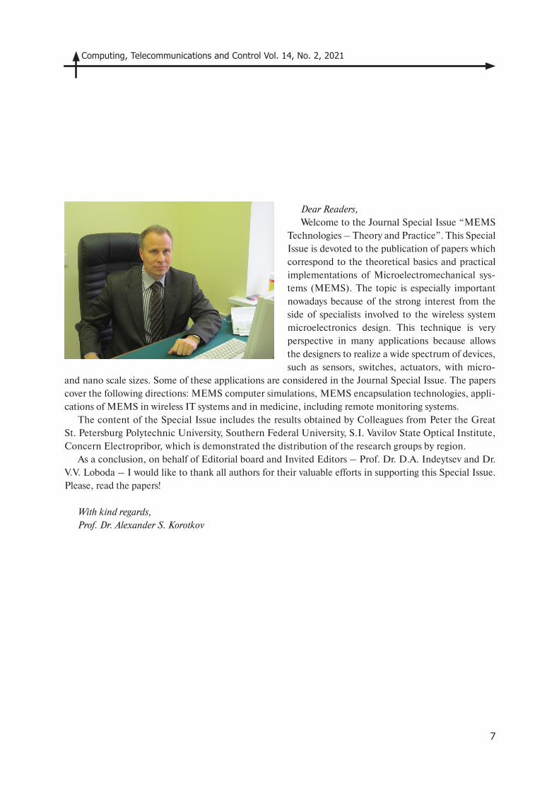
Dear Readers, Welcome to the Journal Special Issue “MEMS
Technologies – Theory and Practice”. This Special Issue is devoted to the publication of papers which correspond to the theoretical basics and practical implementations of Microelectromechanical sys-tems (MEMS). The topic is especially important nowadays because of the strong interest from the side of specialists involved to the wireless system microelectronics design. This technique is very perspective in many applications because allows the designers to realize a wide spectrum of devices, such as sensors, switches, actuators, with micro-
and nano scale sizes. Some of these applications are considered in the Journal Special Issue. The papers cover the following directions: MEMS computer simulations, MEMS encapsulation technologies, appli-cations of MEMS in wireless IT systems and in medicine, including remote monitoring systems.
The content of the Special Issue includes the results obtained by Colleagues from Peter the Great St. Petersburg Polytechnic University, Southern Federal University, S.I. Vavilov State Optical Institute, Concern Electropribor, which is demonstrated the distribution of the research groups by region.
As a conclusion, on behalf of Editorial board and Invited Editors – Prof. Dr. D.A. Indeytsev and Dr. V.V. Loboda – I would like to thank all authors for their valuable efforts in supporting this Special Issue. Please, read the papers!
With kind regards,Prof. Dr. Alexander S. Korotkov
8
DOI: 10.18721/JCSTCS.14201УДК 004.3
DIGITAL MEMS MICROPHONES FOR REMOTE MONITORING SYSTEM BASED ON SOUND ANALYSIS
D.O. Budanov, D.V. Morozov, M.M. PilipkoPeter the Great St. Petersburg Polytechnic University,
St. Petersburg, Russian Federation
Sounds emitted by mechanisms and organisms contain information that can be used to diagnose the current state of an object and make predictions. There are known examples of the use of sound for diagnostics of pipelines, composite materials, industrial equipment. In most cases, devices with one sensor and limited functionality are used for this purpose, requiring a specialist to be in close proximity to the object under analysis. The system includes a set of digital microelectromechanical (MEMS) microphones, information from which is transmitted via Bluetooth to the mobile device. The system in a round-the-clock mode quickly registers changes in the spectrum of the sound signaland indicates possible malfunctions, damage to equipment and materials, etc. This allows preventing irreversible consequences. In this system, it is expedient to use digital MEMS microphones due to their low power consumption and low sensitivity to environmental influences, which is an important factor when deploying a remote monitoring system of industrial equipment.
Keywords: MEMS, digital microphone, piezoelectric microphone, capacitive microphone, Bluetooth, Bluetooth Low Energy, sound analysis.
Citation: Budanov D.O., Morozov D.V., Pilipko M.M. Digital MEMS microphones for remote monitoring system based on sound analysis. Computing, Telecommunications and Control, 2021, Vol. 14, No. 2, Pp. 8–15. DOI: 10.18721/JCST-CS.14201
This is an open access article under the CC BY-NC 4.0 license (https://creativecommons.org/licenses/by-nc/4.0/).
ЦИФРОВЫЕ МЭМС-МИКРОФОНЫ ДЛЯ СИСТЕМЫ ДИСТАНЦИОННОГО МОНИТОРИНГА
НА ОСНОВЕ АНАЛИЗА ЗВУКА
Д.О. Буданов, Д.В. Морозов, М.М. ПилипкоСанкт-Петербургский политехнический университет Петра Великого,
Санкт-Петербург, Российская Федерация
Звуки, издаваемые механизмами и организмами, содержат информацию, которую можно использовать для диагностики текущего состояния объекта и прогноза на будущее. Известны примеры использования звука для диагностики трубопроводов, композитных материалов, промышленного оборудования. В большинстве случаев для этой цели приме-няются устройства с одним датчиком и ограниченным функционалом, требующие нахож-дения специалиста в непосредственной близости к исследуемому объекту. Предлагается система для дистанционного мониторинга, включающая в себя набор датчиков-микрофо-нов, информация с которых передается посредством Bluetooth на мобильное устройство. Система в круглосуточном режиме оперативно регистрирует изменения в спектре звуко-вого сигнала, свидетельствующие о возможных неисправностях, повреждении оборудова-ния и материалов и т. д., что позволяет предупредить необратимые последствия. В данной системе целесообразно применять цифровые МЭМС-микрофоны вследствие их низкого
MEMS Technologies: Theory and Practice
D.O. Budanov, D.V. Morozov, M.M. Pilipko, DOI: 10.18721/JCSTCS.14201
9
энергопотребления и низкой чувствительности к воздействию окружающей среды, что является важным фактором при развертывании системы дистанционного мониторинга промышленного оборудования.
Ключевые слова: МЭМС, цифровой микрофон, пьезоэлектрический микрофон, ёмкост-ной микрофон, Bluetooth, Bluetooth Low Energy, анализ звука.
Ссылка при цитировании: Budanov D.O., Morozov D.V., Pilipko M.M. Digital MEMS micro-phones for remote monitoring system based on sound analysis // Computing, Telecommunica-tions and Control. 2021. Vol. 14. No. 2. Pp. 8–15. DOI: 10.18721/JCSTCS.14201
Cтатья открытого доступа, распространяемая по лицензии CC BY-NC 4.0 (https://creative-commons.org/licenses/by-nc/4.0/).
Introduction
Microelectromechanical systems(MEMS) consist of both microelectronic and micromechanical components. MEMS devices are usually implemented on a silicon substrate. There are two basic types of such devices. Ohmic devices are controlled by electrostatically controlled cantilevers. Capacitive MEMS are developed using a moving plate or a sensing element, which changes the capacitance. There is a wide range of devices that can be implemented using MEMS. They are accelerometers, pressure sensors, thermoelectric generators [1], microphones [2], etc. Using MEMS versions of such devices allows decreasing the device size and power consumption. In some cases, it also leads to reduction in the influence of temperature, vibration and so on.
The important research field is design of high sensitivity digital MEMS microphones for various consumer and industrial electronic applications. They are automobiles, telephones, hearing aids, mo-bile phones, tablet PCs and personal audio systems [2]. Advantages of such microphones are small size, low cost and easy integration with CMOS circuits: the MEMS microphone and its signal processing integrated circuit can be monolithically integrated on a single chip [2]. Also, MEMS microphones have less sensitivity to temperature, vibrations, and mechanical shocks [3]. Therefore, it is preferable to use such type of microphones in remote monitoring systems that carry out surveillance on the object or en-vironment state based on the sound analysis, especially, if such a system works in aharsh environment, for example, an industrial one.
The purpose of the review is to inform the reader with the MEMS microphonesoperation principles, the protocols used for data transmission, the Bluetooth Low Energy (BLE) specification and the archi-tecture of the remote monitoring system based on sound analysis.
Types of MEMS microphones
A microphone is an acoustic-mechanical-electrical sensor that converts acoustical signal into electri-cal one that can be further processed. The analog electrical signal is converted into the digital form by the analog-to-digital converter (ADC) [4, 5]. Then the digital code from the ADC output is converted accord-ing to the protocol (I2S, SPI, etc.) used. After that by the given protocol the data is passed to the further digital devices for processing.
MEMS microphones are widely used in mobile applications such as smartphones, laptops, hearing aids, digital assistants, etc. due to their smaller sizes, higher signal to noise ratio and lower power consump-tion in comparison with traditional electret condenser microphones [6]. Also, as was said before, MEMS microphones have less sensitivity to the environment impacts. Thus, such kind of microphones can be used in remote monitoring systems for industrial applications.
Generally, three types of MEMS microphones are piezoelectric and capacitive [2, 7]. Capacitive MEMS microphones show high sensitivity and CMOS compatibility, while maintaining low power con-sumption [2] and remain the mainstream sensing technology for commercial products [7]. Such kind of microphones usually consists of a diaphragm, a back plate and an air gap. The principle is change in
Computing, Telecommunications and Control Vol. 14, No. 2, 2021
10
voltage by changing in capacitance. The diaphragm is vibrated due to acoustic pressure applied over it. This leads diaphragm and back plate behave as a capacitor [8]. Biased with a DC voltage, the capacitance change is converted into an electrical signal [2]. Capacitive MEMS microphones allow to improve mini- aturization, integration and cost of the acoustic systems by leveraging the MEMS technology [2]. The performance of such kind of microphones can be increased by implementing the special design of the diaphragm and the back plate [7]. However, the structure of the capacitive sensing microphone is fragile to water vapor or dust [7]. This makes an additional water/dustproof packaging needed for such microphone when using in the harsh environment. The requirement of such special packaging leads to increasing the microphone cost. On the other hand, the piezoelectric sensing microphone could tolerate the influence of harsh environment [7] and has more robust mechanical structure with no air gap [9]. The piezoelectric sensing is performed by converting mechanical stress into electrical charge[10]. In such microphone the sensitivity is based on the properties of piezoelectric elements [11]. Piezoelectric MEMS microphones are extensively studied to improve acoustic performance [7]. Many approaches such as structure design, material usage, stress distribution, etc. have been proposed to improve performance of the piezoelectric microphone [7]. However, the enhancement of the piezoelectric film stress induced by the sound pressure and the air leakage from gaps between the diaphragm remain design concerns [7].
MEMS microphones can also be divided into two types: omnidirectional and unidirectional [6]. The omnidirectional microphonegenerates an electrical response from acoustic energy arriving from all di-rections around the device. Most of these microphones are capacitive ones [6]. The unidirectional mi-crophone has its strongest output when acoustical energy arrives along a single axis vertical through or parallel with the surface of a vibrational membrane [6]. Both types of microphones can be used in a remote monitoring system for sound capturing. Omnidirectional microphones are applied when the system have to seize surrounding sounds, for example, from the nearby devices or equipment. Unidirectional micro-phones are used for surveillance over the specified equipment among others or over the specified part/location of the given equipment.
Communication protocols
After analog-to-digital conversion of the microphone output signal has been completed, the digital signal has to be formed from the ADC output bits according to the interface protocolused. This interface can be integrated with a MEMS microphone if CMOS-compatible technology is used.The high-speed protocol is needed for audio data transferring. There are several protocols or standards, such as SPI and I2S, that satisfy requirements for audio data transferring.
Serial Peripheral Interface (SPI) is a synchronous serial communication interface specification [12]. Devices can communicate over SPI in full duplex mode. The architecture with a single master and mul-tiple slave devices is used.The master device generates the frame for reading and writing. Also, the master device selects a slave devicefor data transferring by activating the chip select signal on the latter. Slave de-vices not selected by the master do not participate in the data transferring. The SPI bus has four logic lines:
• SCLK or SCK – serial clock transferring from master to slave devices;• MISO – Master In, Slave Out – data output from slave device;• MOSI – Master Out, Slave In – data output from master device;• SS or CS – Slave Select or Chip Select – this signal is set by the master device.The SCLK clock signal generated by the master device sets the clock rate in the bus. Slave devices use
this clock signal to determine when the data bits in the bus change.Data transferring is carried out in packets. Usually, the packet length is 1 byte (8 bits). However, SPI
implementations with various packet length are known. The master device initiates data transferring by setting the SS pin of the slave device to be connected to logic low. Data are transferred from the master to slave over the MOSI line and from the slave to master over the MISO line. After each data packet transfer the master device can set the SS line to the logic high for synchronization.
D.O. Budanov, D.V. Morozov, M.M. Pilipko, DOI: 10.18721/JCSTCS.14201
11
Inter-IC Sound (I2S) is a serial interface standard used for connecting digital audio devices [13]. The I2S bus has three lines:
• SCK or BCLK – continuous serial clock or bit clock;• WS – word select or word clock line;• SD – serial data.The master device generates both SCK and WS clock signals. Slave devices will usually derive its inter-
nal clock signal from the external clock input.Since the transmitter and receiver have the same clock signal for data transferring, the transmitter as the
master has to generate the SCK signal, WS signal and data. In complex systems, there may be several trans-mitters and receivers, which makes it difficult to determine the master. In such systems, there is usually a system master controlling digital audio data-flow between the various devices. In this case, transmitters have to generate data under the control of an external clock, and thus act as a slave device [13].
Some digital MEMS microphones support only the pulse-density modulated (PDM) output [14, 15]. To communicate with these microphones SPI and I2S interfaces can be used. Usually, a PDM micro-phone has three lines:
• LR – left/right channel selection (input pin);• CLK – input synchronization clock signal;• DOUT – left/right PDM data output.The LR pin is used to seize the stereo signal from two microphones. This pin can be connected to Vdd
or GND bus to operate in the mono mode.The PDM data can be further received and processed by the microcontroller unitusing its available in-
terfaces, such as SPI, I2S or SAI (Serial Audio Interface) [14]. Then, this data can be transferred via wired or wireless (Wi-Fi, Bluetooth, etc.) communication channel.
Bluetooth Low Energy
Bluetooth Low Energy (BLE, also known as Bluetooth Smart) started as part of the Blue-tooth 4.0 Core Specification [16]. Both Bluetooth Classic and Bluetooth Low Energy operate in the 2400–2483.5 MHz frequency range within the ISM 2.4 GHz frequency band. The data exchange in Bluetooth Classic happens over one of the 79 designated channels, while in Bluetooth Low Energy the number of designated channels is 40 [17]. The BLE power consumption is from 0.01 to 0.5 W and 1 W for Bluetooth Classic. The physical data rate of Bluetooth Low Energy is 1 Mbit/s, while for Bluetooth Classic this parameter can be up to three times greater reaching 1–3 Mbit/s. However, the latency of BLE is at least 10 times smaller in comparison with a classic Bluetooth, and is 6 ms and 100 ms respec-tively. The theoretical Bluetooth Low Energy working range is more than 100 meters. The minimum total time required to send data in BLE is 33 times less than that in Bluetooth Classic amounting to 3 ms and 100 ms respectively. Point-to-point and star network topologies are usually used in Bluetooth Low Energy, while piconet, scatternet and point-to-point topologies can be deployed in Bluetooth Classic [17]. A device in a BLE network can be a server or a client. The server is a peripheral device that trans-mits data from sensors or receives commands to manage devices connected to BLE module or transmits data to these devices. The client is a device that receives data from sensors or sends commands to man-age devices connected to BLE module. Bluetooth Low Energy is commonly used for interacting with a wide set of sensors due to its low power consumption. However, there is no standard way of transmitting voice over BLE, consequentlya custom profile must be used [18].
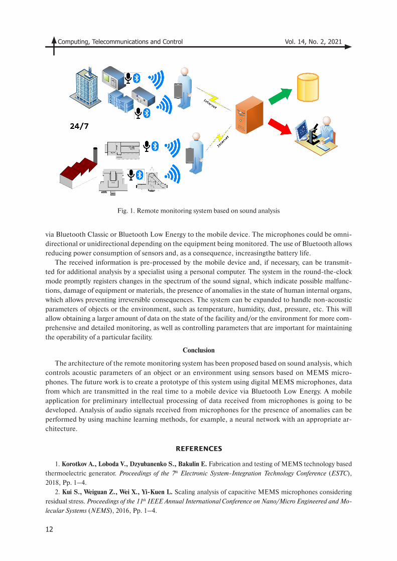
System architecture
The architecture of the remote monitoring system based on sound analysis is presented in Fig. 1. It can be used for diagnostics of expensive industrial equipment and unique laboratory and research facil-ities. The system includes a set of digital MEMS microphones, information from which is transmitted
Computing, Telecommunications and Control Vol. 14, No. 2, 2021
12
via Bluetooth Classic or Bluetooth Low Energy to the mobile device. The microphones could be omni-directional or unidirectional depending on the equipment being monitored. The use of Bluetooth allows reducing power consumption of sensors and, as a consequence, increasingthe battery life.
The received information is pre-processed by the mobile device and, if necessary, can be transmit-ted for additional analysis by a specialist using a personal computer. The system in the round-the-clock mode promptly registers changes in the spectrum of the sound signal, which indicate possible malfunc-tions, damage of equipment or materials, the presence of anomalies in the state of human internal organs, which allows preventing irreversible consequences. The system can be expanded to handle non-acoustic parameters of objects or the environment, such as temperature, humidity, dust, pressure, etc. This will allow obtaining a larger amount of data on the state of the facility and/or the environment for more com-prehensive and detailed monitoring, as well as controlling parameters that are important for maintaining the operability of a particular facility.
Conclusion
The architecture of the remote monitoring system has been proposed based on sound analysis, which controls acoustic parameters of an object or an environment using sensors based on MEMS micro-phones. The future work is to create a prototype of this system using digital MEMS microphones, data from which are transmitted in the real time to a mobile device via Bluetooth Low Energy. A mobile application for preliminary intellectual processing of data received from microphones is going to be developed. Analysis of audio signals received from microphones for the presence of anomalies can be performed by using machine learning methods, for example, a neural network with an appropriate ar-chitecture.
Fig. 1. Remote monitoring system based on sound analysis
REFERENCES
1. Korotkov A., Loboda V., Dzyubanenko S., Bakulin E. Fabrication and testing of MEMS technology based
thermoelectric generator. Proceedings of the 7th Electronic System-Integration Technology Conference (ESTC),
2018, Pp. 1–4.
2. Kui S., Weiguan Z., Wei X., Yi-Kuen L. Scaling analysis of capacitive MEMS microphones considering
residual stress. Proceedings of the 11th IEEE Annual International Conference on Nano/Micro Engineered and Mo-
lecular Systems (NEMS), 2016, Pp. 1–4.
D.O. Budanov, D.V. Morozov, M.M. Pilipko, DOI: 10.18721/JCSTCS.14201
13
3. Lei L., Kechao L., Jintao F., Pengfei Z., Zhiyong H., Ce G. Acoustic enhanced camera tracking system
based on small-aperture MEMS microphone array. IEEE Access, 2020, Vol. 8, Pp. 215827–215839.
4. Piatak I., Pilipko M., Morozov D. A 14-bit 50-MS/s pipelined analog-to-digital converter with digi-
tal error calibration. Proceedings of the 2015 International Siberian Conference on Control and Communications
(SIBCON), 2015, Pp. 1–4.
5. Budanov D.O., Morozov D.V., Pilipko M.M. An 8-bit analog-to-digital converter with a novel encoder
using 90 nm CMOS. Proceedings of the 2018 IEEE International Conference on Electrical Engineering and Pho-
tonics (EExPolytech), 2018, Pp. 56–59.
6. Zhang Y., Bauer R., Jackson J.C., Whitmer W.M., Windmill J.F.C., Uttamchandani D. A low-frequen-
cy dual-band operational microphone mimicking the hearing property of ormia ochracea. Journal of Micro-
electromechanical Systems, 2018, Vol. 2, Issue 4, Pp. 667–676.
7. Tseng S.-H., Lo S.-C., Chen Y.-C., Lee Y.-C., Wu M., Fang W. Implementation of piezoelectric MEMS
microphone for sensitivity and sensing range enhancement. Proceedings of the IEEE 33rd International Confer-
ence on Micro Electro Mechanical Systems (MEMS), 2020, Pp. 845–848.
8. Jain J., Tripathy M.R. Study of MEMS technology and development of condenser microphone. Pro-
ceedings of the 5th International Conference – Confluence The Next Generation Information Technology Summit
(Confluence), 2014, Pp. 880–882.
9. Segovia-Fernandez J., Sonmezoglu S., Block S.T., Kusano Y., Tsai J.M., Amirtharajah R., Horsley D.A.
Monolithic piezoelectric Aluminum Nitride MEMS-CMOS microphone. Proceedings of the 19th International
Conference on Solid-State Sensors, Actuators and Microsystems (TRANSDUCERS), 2017, Pp. 414–417.
10. Chen Y.-C., Lo S.-C., Cheng H.-H., Wu M., Huang I.-Y., Fang W. Design of cantilever diaphragm
array piezoelectric MEMS microphone for signal-to-noise ratio enhancement. Proceedings of the 2019 IEEE
SENSORS, 2019, Pp. 1–4.
11. Muralidhar Y.C., Neethu K.N., Nagaraja V.S., Pinjare S.L. Design and simulation of polymer piezo-
electric MEMS microphone. Proceedings of the 2013 International Conference on Circuits, Controls and Commu-
nications (CCUBE), 2013, Pp. 1–4.
12. Introduction to SPI Interface. Available: https://www.analog.com/en/analog-dialogue/articles/introduc-
tion-to-spi-interface.html (Accessed: 14.05.2021).
13. I2S bus specification. Available: https://www.sparkfun.com/datasheets/BreakoutBoards/I2SBUS.pdf
(Accessed: 14.05.2021).
14. Interfacing PDM digital microphones using STM32 MCUs and MPUs. Available: https://www.st.com/re-
source/en/application_note/dm00380469-interfacing-pdm-digital-microphones-using-stm32-mcus-and-mpus-st-
microelectronics.pdf (Accessed: 14.05.2021).
15. MP34DT01-M, Digital MEMS microphone. Available: https://www.st.com/en/audio-ics/mp34dt01-m.
html#overview (Accessed: 14.05.2021).
16. Townsend K., Cufi C., Davidson A., Davidson R. Getting Started with Bluetooth Low Energy: Tools and
Techniques for Low-Power Networking. O'Reilly Media, 2014, 282 p.
17. Bhargava M. IoT Projects with Bluetooth Low Energy. Packt Publishing, 2017, 377 p.
18. Voice over BLE. Available: http://software-dl.ti.com/lprf/simplelink_cc2640r2_sdk/1.35.00.33/exports/
docs/ble5stack/ble_user_guide/html/voice/ble_voice.html (Accessed: 14.05.2021).
Received 23.05.2021.
СПИСОК ЛИТЕРАТУРЫ
1. Korotkov A., Loboda V., Dzyubanenko S., Bakulin E. Fabrication and testing of MEMS technology
based thermoelectric generator // Proc. of the 7th Electronic System-Integration Technology Conf. 2018.
Pp. 1–4.
Computing, Telecommunications and Control Vol. 14, No. 2, 2021
14
2. Kui S., Weiguan Z., Wei X., Yi-Kuen L. Scaling analysis of capacitive MEMS microphones considering
residual stress // Proc. of the 11th IEEE Annual Internat. Conf. on Nano/Micro Engineered and Molecular
Systems. 2016. Pp. 1–4.
3. Lei L., Kechao L., Jintao F., Pengfei Z., Zhiyong H., Ce G. Acoustic enhanced camera tracking system
based on small-aperture MEMS microphone array // IEEE Access. 2020. Vol. 8. Pp. 215827–215839.
4. Piatak I., Pilipko M., Morozov D. A 14-bit 50-MS/s pipelined analog-to-digital converter with digital
error calibration // Proc. of the 2015 Internat. Siberian Conf. on Control and Communications. 2015. Pp. 1–4.
5. Budanov D.O., Morozov D.V., Pilipko M.M. An 8-bit analog-to-digital converter with a novel encoder
using 90 nm CMOS // Proc. of the 2018 IEEE Internat. Conf. on Electrical Engineering and Photonics. 2018.
Pp. 56–59.
6. Zhang Y., Bauer R., Jackson J.C., Whitmer W.M., Windmill J.F.C., Uttamchandani D. A low-frequency
dual-band operational microphone mimicking the hearing property of ormia ochracea // J. of Microelectrome-
chanical Systems. 2018. Vol. 2. Issue 4. Pp. 667–676.
7. Tseng S.-H., Lo S.-C., Chen Y.-C., Lee Y.-C., Wu M., Fang W. Implementation of piezoelectric MEMS
microphone for sensitivity and sensing range enhancement // Proc. of the IEEE 33rd Internat. Conf. on Mi-
cro Electro Mechanical Systems. 2020. Pp. 845–848.
8. Jain J., Tripathy M.R. Study of MEMS technology and development of condenser microphone // Proc.
of the 5th Internat. Conf.– Confluence the Next Generation Information Technology Summit (Confluence).
2014. Pp. 880–882.
9. Segovia-Fernandez J., Sonmezoglu S., Block S.T., Kusano Y., Tsai J.M., Amirtharajah R., Horsley D.A.
Monolithic piezoelectric Aluminum Nitride MEMS-CMOS microphone // Proc. of the 19th Internat. Conf. on
Solid-State Sensors, Actuators and Microsystems (TRANSDUCERS). 2017. Pp. 414–417.
10. Chen Y.-C., Lo S.-C., Cheng H.-H., Wu M., Huang I.-Y., Fang W. Design of cantilever diaphragm array
piezoelectric MEMS microphone for signal-to-noise ratio enhancement // Proc. of the 2019 IEEE SENSORS.
2019. Pp. 1–4.
11. Muralidhar Y.C., Neethu K.N., Nagaraja V.S., Pinjare S.L. Design and simulation of polymer pie-
zo-electric MEMS microphone // Proc. of the 2013 Internat. Conf. on Circuits, Controls and Communica-
tions. 2013. Pp. 1–4.
12. Introduction to SPI Interface // URL: https://www.analog.com/en/analog-dialogue/articles/introduc-
tion-to-spi-interface.html# (Дата обращения: 14.05.2021).
13. I2S bus specification // URL: https://www.sparkfun.com/datasheets/BreakoutBoards/I2SBUS.pdf
(Дата обращения: 14.05.2021).
14. Interfacing PDM digital microphones using STM32 MCUs and MPUs // URL: https://
www.st.com/resource/en/application_note/dm00380469-interfacing-pdm-digital-microphones-us-
ing-stm32-mcus-and-mpus-stmicroelectronics.pdf (Дата обращения: 14.05.2021).
15. MP34DT01-M, Digital MEMS microphone // URL: https://www.st.com/en/audio-ics/mp34dt01-m.
html#overview (Дата обращения: 14.05.2021).
16. Townsend K., Cufi C., Davidson A., Davidson R. Getting started with bluetooth low energy: Tools and
techniques for Low-Power Networking. O'Reilly Media, 2014. 282 p.
17. Bhargava M. IoT projects with Bluetooth Low Energy. Packt Publishing, 2017. 377 p.
18. VoiceoverBLE // URL: http://software-dl.ti.com/lprf/simplelink_cc2640r2_sdk/1.35.00.33/exports/
docs/ble5stack/ble_user_guide/html/voice/ble_voice.html (Дата обращения: 14.05.2021).
Статья поступила в редакцию 23.05.2021.
D.O. Budanov, D.V. Morozov, M.M. Pilipko, DOI: 10.18721/JCSTCS.14201
15
THE AUTHORS / СВЕДЕНИЯ ОБ АВТОРАХ
Budanov Dmitry O.Буданов Дмитрий ОлеговичE-mail: [email protected]
Morozov Dmitry V.Морозов Дмитрий ВалерьевичE-mail: [email protected]
Pilipko Mikhail M.Пилипко Михаил МихайловичE-mail: [email protected]
© Санкт-Петербургский политехнический университет Петра Великого, 2021
Computing, Telecommunications and Control Vol. 14, No. 2, 2021
16
DOI: 10.18721/JCSTCS.14202УДК 621.318.51, 621.3.049.7
APPLICATION OF THE RF MEMS TECHNOLOGY IN MODERN WIRELESS SYSTEMS: A POTENTIAL
THAT HAS NOT YET BEEN FULLY REALIZED
I.E. Lysenko, A.V. TkachenkoSouthern Federal University,
Rostov-on-Don, Russian Federation
Today one of the key triggers of the development of research and development in the field of electronics, radio-frequency components, and systems, system integration and design, as well as information and communication technologies are such data network concepts as the Internet of Things, Internet of Everything, Tactical Internet and the most important among them is 5G – the 5th generation of mobile radio communications. This article presents a vision for the use of devices manufactured using microelectromechanical systems technology, namely passive radio-frequency microelectromechanical devices and systems in synergy with energy-harvesting microelectromechanical devices and systems in such new structural paradigms. The authors present their results on the development, manufacture and research of experimental samples of radio-frequency microelectromechanical switches that can meet the growing need for cutting-edge performance for currently deployed 5G NR FR1 (below 6 GHz) mobile networks or high-performance applications.
Keywords: MEMS, RF MEMS, EH MEMS, microelectromechanical systems, radio-frequency, energy-harvesting, modern wireless systems.
Citation: Lysenko I.E., Tkachenko A.V. Application of the RF MEMS technology in modern wireless systems: A potential that has not yet been fully realized. Computing, Telecommunications and Control, 2021, Vol. 14, No. 2, Pp. 16–28. DOI: 10.18721/JCST-CS.14202
This is an open access article under the CC BY-NC 4.0 license (https://creativecommons.org/licenses/by-nc/4.0/).
ПРИМЕНЕНИЕ РЧ МЭМС-ТЕХНОЛОГИИ В СОВРЕМЕННЫХ БЕСПРОВОДНЫХ СИСТЕМАХ:
ПОТЕНЦИАЛ, КОТОРЫЙ ЕЩЁ ПОЛНОСТЬЮ НЕ РАСКРЫТ
И.Е. Лысенко, А.В. ТкаченкоЮжный федеральный университет,
г. Ростов-на-Дону, Российская Федерация
На сегодняшний день одним из ключевых драйверов (триггеров) развития научно- исследовательских и опытно-конструкторских разработок в области электроники, радио-частотных компонентов и систем, системной интеграции и проектирования, а также ин-формационно-коммуникационных технологий являются такие концепции сети передачи данных, как Интернет Вещей, Интернет Всего, Тактильный Интернет и наиболее важный среди них – 5G – пятое поколение мобильной радиосвязи. В статье представлено видение использования устройств, изготовленных с применением технологии микроэлектроме-ханических систем: пассивных радиочастотных микроэлектромеханических устройств и систем в синергии с энергособирающими микроэлектромеханическими устройствами и системами в новых структурных парадигмах. Представлены результаты разработки, изго-товления и исследования экспериментальных образцов радиочастотных микроэлектроме-
I.E. Lysenko, A.V. Tkachenko, DOI: 10.18721/JCSTCS.14202
17
ханических переключателей, способные удовлетворить растущую потребность в ультрасо-временной производительности для развертываемых в настоящее время мобильных сетей 5G NR FR1 (менее 6 ГГц) или высокопроизводительных приложений.
Ключевые слова: МЭМС, РЧ МЭМС, ЭС МЭМС, микроэлектромеханические системы, радиочастотные, энергособирающие, современные беспроводные системы.
Ссылка при цитировании: Lysenko I.E., Tkachenko A.V. Application of the RF MEMS technology in modern wireless systems: A potential that has not yet been fully realized // Computing, Tele- communications and Control. 2021. Vol. 14. No. 2. Pp. 16–28. DOI: 10.18721/JCSTCS.14202
Cтатья открытого доступа, распространяемая по лицензии CC BY-NC 4.0 (https://creative-commons.org/licenses/by-nc/4.0/).
Introduction
In 1835, Joseph Henry invented the first electromechanical device, called a “switch” or “relay”. It consisted of a bulky electromagnet that activated an armature capable of making physical contact between the two electrodes. The clock frequency was limited to tens of hertz.
In 1979, Petersen developed the first micromechanical membrane switches, which were said to fill a niche or fill a gap between conventional silicon transistors with mechanical and electromagnetic relays. This was the starting point that opened the way to microelectromechanical systems (MEMS). The key idea, an original concept at the time, was to combine the capabilities of silicon-based micro-manufac-turing with a mechanical relay approach. The proposed MEMS based switch used an electrostatic force applied between a layer of p-doped silicon and a membrane made of a bimetallic material (SiO
2 content
and Au) to set in motion a movable suspended structure and establish electrical contact.In the 1990s, the electrical and microwave community contributed to the emergence of a new class of
devices: microrelays capable of processing analog, radio-frequency (RF), and microwave signals.In 1990, Halg introduced the first integrated microelectromechanical non-volatile memory cell. In
1991, Larson et al. [1] demonstrated the microwave rotary switch of the transmission line. Measure-ments made up to 45 GHz were already impressed with insertion loss below –0.5 dB and isolation above –35 dB. In 1995, Goldsmith et al. [2] introduced what was to become one of the most well-known membrane configurations for RF microelectromechanical system switches with capacitive contact. Then came the era of RF MEMS [3].
The presented article consists of two parts. The first and main part gives a brief overview of the place of RF MEMS devices in consolidation with the technology of energy-harvesting MEMS devices, and how these technical solutions can contribute to miniaturization, reduce energy consumption, expand possi-ble connections and their efficiency, pursued by the currently developing paradigms of the 5G mobile network, the Internet of Things, the Internet of Everything and the Tactile Internet. The second part of the article presents a brief description of the current research results carried out by this team of authors, the main purpose of which is to develop, manufacture and study experimental samples of single-pole sin-gle-throw RF MEMS switches suitable for use in RF transceiver modules of 5G mobile networks in the frequency band NR FR1.
Principles of operation
RF MEMS systems concentrated passive components that implement functions of varying complexity designed to generate and/or redirect one or more RF signals in the circuits and subsystems of wireless transceivers (transmitters/receivers). In RF MEMS, the ability to reconfigure the conditioning function operating on RF signals is always provided by the physical movement and mechanical deformation of the micromembranes, i.e., the fundamental characteristic of sensors and actuators based on MEMS. Given this context, whatever the complexity of the network-controlled air conditioning function in RF MEMS technology is, the main element is the switch (or relay). As with traditional electromechanical relays, RF
Computing, Telecommunications and Control Vol. 14, No. 2, 2021
18
MEMS switches are equipped with a metal (or more generally conductive) flexible membrane that, when properly deformed, closes the electrical contact between the input and output ends, allowing the RF sig-nal to pass through the relay and change its state from open to closed. On the other hand, unlike classical devices, RF MEMS switches are highly miniaturized, and the dimensions in the plane can reach several tens of microns, and the thickness (out-of-plane size) is only a few microns (or from 50 μm to 100 μm, also considering the silicon substrate). The most common actuation strategy for controlling the movement of a moving contact, and therefore for controlling the state transition between open and closed, is electrostatic displacement. Voltage (i.e. displacement) is superimposed on the floating part and the fixed actuation electrode, and the force of displacement brings the first electrode into physical contact with the input and output branches, thereby closing them and closing the relay.
However, in addition to the electrostatic force [4, 5], other actuation mechanisms are possible, such as thermoelectric [6], piezoelectric [7] and electromagnetic [8]. In addition, depending on the specific deployment and configuration of the I/O electrodes, the switch can be ohmic or capacitive, as well as serial or shunt, which provides the developer with various degrees of freedom and covers a wide range of performance and performance characteristics.
Essentially, starting with basic reconfigurable elements, i.e. ohmic and capacitive, micro-relays with excellent performance in terms of high isolation, wide frequency range, low insertion loss, pronounced linearity, and almost zero power consumption, proper redundancy, and interconnection enable the im-plementation of high-performance and widely reconfigurable passive RF MEMS networks [9]. Since then, switching blocks have been successfully demonstrated in the literature, ranging from single-pole double-throws (SPDTs) to more complex single-pole multiple-throws (SPMTs) and switching matrices. Reconfigurable RF power attenuators and splitters/couplers can also be fully implemented in RF MEMS technology, as well as in impedance matching tuners covering a significant portion of the smith-diagram and implementing a large number of different states. In addition, RF MEMS technology has been proven to be a key solution that also allows the implementation of reconfigurable phase shifters and true time delay lines (TDL) for electronic antenna steering and radar systems, as well as in the micro-fabrication of tunable filters for various RF applications.
Market expectations
Among the various concepts outlined by Nguyen in 2001, it is certainly one of the most relevant [10]. Starting with the standard transceiver architecture (transmitter/receiver), the deployment of RF MEMS had to follow two paths. At the first stage, it was assumed that the RF passives in MEMS technology, such as antenna switches, RF/IF (intermediate frequency) filters, LC reservoirs, and resonators, would replace the standard counterparts, increasing the system performance. The second stage of the development of a high-precision RF MEMS device, such as multi-channel selectors with built-in filtering functions and mixer filters, would cause a rethink of the transceiver architecture. The block diagram of RF systems had to be simplified, which would reduce both hardware complexity and power consumption. This transmission topology can provide huge energy savings. In particular, if a high-Q and high-power filter with an insertion loss of less than 1 dB can follow the power amplifier (PA), clearing all spurious outputs, including those re-sulting from spectrum overgrowth, then more efficient PA designs can be used, despite their non-linearity. For example, a PA previously limited by linearity considerations to 30 % efficiency in modern transmitter architectures may be operational closer to its maximum efficiency, perhaps 50 %. For a typical transmis-sion capacity of 600 mW, this efficiency improvement corresponds to an energy saving of 800 mW. The performance of the transceiver, on the other side, would be expanded by numerous standards and services. Nevertheless, the evolution of the facts went in a completely different direction. Market forecasts pub-lished since the early 2000s envisioned hundreds of millions of dollars (US dollars) for RF MEMS in the consumer market segment, which, analysis by analysis, were systematically reduced. These disappoint-ments occurred for two reasons, both internal and external to the technology itself.
I.E. Lysenko, A.V. Tkachenko, DOI: 10.18721/JCSTCS.14202
19
At the same time, the first successes in the development of passive RF MEMS components were an-nounced only in the last few years, with a delay of about one decade compared to the market revolution predicted in the early 2000s. This was due to the fact that the rather critical aspects of RF MEMS technol-ogy were not fully evaluated at the beginning.
Internal factors were associated with the lack of maturity of RF MEMS in the early years of their discus-sion, with a particular focus on reliability, packaging, and integration with other (incompatible) technologies. On the other hand, external factors correlated with the surrounding market environment. In fact, mobile apps prior to 3G–3.5 G were not really demanding on high-performance components, such as RF MEMS.
The context of the link began to change with the appearance of 4G-LTE mobile devices (4th genera-tion; Long-Term Evolution). The inclusion of an increasing number of components has caused a gradual trend towards a deterioration in the quality of communication. The antennas no longer functioned under optimal conditions, resulting in lower download speeds, lower voice quality, lower energy efficiency, and more missed calls. The fixed impedance matching between the antenna and the RF front-end (RFFE), classically adopted in previous generations of mobile phones, was no longer the best option. As part of this, for example, for a few years, adaptive RF MEMS impedance tuners have begun to make their way into the consumer segment of the 4G-LTE smartphone market.
Next up is the 5th generation of mobile networks and devices. 5G seems to be the right platform for RF MEMS technology to express its full potential in market applications.
The development scenario of 5G
5G will implement a completely different paradigm compared to 4G, 4G-LTE. Some of the services we use today, such as Wi-Fi internet access and video streaming, will be covered by 5G coverage along with classic features such as voice calls and mobile internet access. It is also important to note that ma-chine-to-machine (M2M) communication data is expected to be transmitted over 5G protocols. Exam-ples of M2M applications are autonomous vehicles, remote surgery, remote manufacturing, and smart cities. In other words, a significant portion of the Internet of Things (IoT), Internet of Everything (IoE) data traffic will depend on 5G networks.
Obviously, the data throughput requirement is going to be huge. Many forecasts call for a 1000-fold increase in 5G transmission capacity over 4G-LTE, providing 10 Gb/s for each individual user. In addi-tion, the data transfer delay will need to be drastically reduced to a millisecond level. To understand the importance of the latter requirement, one can simply wonder how low latency can be critical for appli-cations such as vehicle-to-vehicle (V2V) communication. Finally, more importantly, when using M2M applications, cloud computing, IoT, IoE, and so on, will require a greater symmetry between the downlink and uplink bandwidth of the 5G standard.
How this revolution will become possible at the implementation level is still a hot topic for discussion. Nevertheless, some high-level trends have already begun to show up quite clearly. 5G radio access technol-ogies (RATs) will use three main components to increase the amount of data transmitted [11]:
1. The order of modulation;2. Aggregated throughput;3. The order of multiple-input and multiple-output antennas (MIMO).If the first degree of freedom is a problem mainly at the level of algorithms and electronic design, points
2 and 3 make clear requirements in terms of hardware reconfiguration. In particular, improving aggre-gated bandwidth means increasing the number of carrier aggregation (CA) components. Translated into the technical characteristics of the equipment, this means that RF transceivers must have high readjusted ability and flexibility in the rapid transition from one frequency band to another. On the other hand, in-creasing the order of MIMO means having arrays/arrays of integrated antennas (e.g. 4 × 4) small enough for use in smartphones and controlled by high-performance RFFEs with improved switching and filtering characteristics to minimize internal and crosstalk.
Computing, Telecommunications and Control Vol. 14, No. 2, 2021
20
From the point of view of mobile infrastructure, another trend towards consolidation is the spread of frequencies across the entire reverse part of the network hierarchy. In this regard, a clear frequency divi-sion will characterize 5G networks. The classic macronutrients, covering quite extensive areas, will mostly operate in the range up to 6 GHz. On the other hand, the huge data throughput mentioned above will be achieved by significantly compacting the network. For this purpose, small cells will be deployed that cover very limited spaces, such as a single building or small metropolitan areas (for example, the lobby of a train station or shopping center). Such small cells will allow mass data transmission in the millimeter wave range, that is, significantly higher than 6 GHz. On the other hand, they will require arrays of reconfigur-able antennas and RF drivers capable of implementing advanced signal shaping and, in turn, achieving pronounced directivity and effective coverage of the zone.
So, both in terms of mobile phones and infrastructure, 5G will require high frequency flexibility and reconfiguration. RF transceivers must be very flexible in combining multiple components operating at several GHz (below –6 GHz), as well as up to 60–70 GHz (millimeter wave range). In addition, you will need integrated arrays of antennas and RFFE with increased performance, both to increase the order of MIMO, and to solve the problem of signal formation.
It is possible to distinguish these functional characteristics in the specification that must be achieved by passive RF components:
1. Very wideband switches and switching units (such as multi-pole multi-throw MPMT) with low loss (on-off), high isolation (on-off), and very low crosstalk of adjacent channels, operating from 2 to 3 GHz to 60–70 GHz (or more);
2. Reconfigurable filters with pronounced bandwidth suppression and very low bandwidth attenuation;3. Very wide-band multi-position impedance tuners;4. Programmable step attenuators with multiple configurations and very flat response in the 60–70 GHz
frequency range;5. Very wide-band multi-position / analog phase shifters;6. Hybrid devices with mixed phase shift and programmable attenuation – the functionality described
in paragraphs 4 and 5 is combined into a unique device;7. Miniature antennas and arrays of antennas, possibly integrally integrated with one or more of the
devices described in the previous paragraphs from 1 to 6.Given these classes of devices, the RF characteristics they will need to achieve can be summarized as
follows:– Isolation: better than –30/–40 dB for frequencies as high as possible;– Loss: below –1 dB in the widest possible frequency range;– Cross-talk: below –50/–60 dB in the widest frequency range;– Switching time: less than 1 ms, with a few fractions of μs (e.g. 200–300 μs) as a reasonable target;– Control voltage: within a few volts (for example, 2–5 V).To summarize, it should be noted that first, the above specifications and limitations can be solved using
MEMS technology. In addition, RF MEMS allows you to combine different functionality, which opens up interesting opportunities in terms of reducing hardware complexity. In this regard, it is worth mentioning the possibility of implementing reconfigurable phase shift and programmable attenuation of RF signals using unique passive components, which can also be integrated with an array of antennas in the millim-eter wavelength range. Therefore, if RF MEMS components are currently on the path of consolidation in 4G-LTE applications, in the future 5G scenario, they have a significantly large role and large market volumes, both in relation to mobile phones and terrestrial infrastructures.
The synergy of RF and energy-harvesting MEMS
The energy-harvesting (EH) power availability driver deserves a more detailed discussion, as it should be compared to the typical power requirements of IoT nodes.
I.E. Lysenko, A.V. Tkachenko, DOI: 10.18721/JCSTCS.14202
21
Simply put, remote sensing nodes (always) consist of three main parts [12]:1. Sensitive module (sensor, electronic reading interface);2. Computing unit (Microcontroller unit – MCU);3. RF transceiver.Such blocks are the most energy-intensive, and energy consumption, in general terms, increases when
moving from point 1 to point 3. The typical power ranges required by the three remote sensing modules are as follows:
1. Sensor assembly 1 μW–1050 μW;2. Normal operation of the MCU 100 μW–15 mW;3. RF transceiver: 1520 mW–100 mW or more.The energy dissipated in the environment can be obtained from four different sources: 1) ambient light;
2) vibration/motion; 3) thermal energy; 4) RF energy. Each of them has different achievable power levels, also depending on the operating conditions (indoor/outdoor, human/industrial environment, etc.).
Currently, research has advanced fueled by the continuous trend of reducing the power consumption of integrated circuits (IC). This paved the way for the use of MEMS technology for EH, using piezoelectric, electromagnetic and electrostatic conversion mechanisms [13].
The fundamental problem resulting from EHs miniaturization is the scaling of the operating frequency, since the resonant frequency of vibrating devices increases with decreasing mass and geometry, while most of the ambient vibration energy is available below a few kHz. There are solutions to solve this problem based on converting the frequency of ambient vibration. For example, complementary magnets can pro-vide a resonant structure with a broadband pulse that also covers the main resonant frequency. The EH in [14] generates power up to 65 μW (RMS) for oscillations up to 12 Hz. Other upconversion approaches use snap and bend induced pulses superimposed on a microtransformer.
Another limitation affecting EHs MEMS is used in a typically narrow frequency band. Vibrational resonance is mechanical resonators that exhibit the greatest vibrations at resonance and filter out most of the spectrum elsewhere. There is extensive literature on strategies and methods for expanding the response to vibrational EH MEMS.
The frequency response of the devices demonstrates a chaotic response (the resonance of the Duffing mode) when the elastic behavior of the vibration-proof masses is nonlinear. This expands the frequency range of the radiation and, in turn, the level of the extracted power. In the literature, hybrid solutions based on piezoelectric and electromagnetic energy converters are discussed, which also differ in frequency con-version up using folded cantilever structures. The tuning of the resonant frequency EH is investigated to maximize the extraction in the widest possible range of operability.
EHs vibration consists of duplicating and changing the main elements of the spring mass. For this pur-pose, the solution proposed in [15] uses a two-resonant structure to implement an electrostatic EH MEMS of 13 × 20 mm2. The entire design has two resonant frequencies, leading the EH to power levels in the range of 1.063 μW (1 g acceleration) in the frequency range of approximately 140 to 190 Hz.
As for the thermoelectric EH, the fundamental principle of converting thermal energy into electricity is the Seebeck effect, which describes the electromotive force that occurs when a thermal gradient is applied to the connection of two different materials. MEMS and film technology contributed to the development of miniature thermoelectric EHs. For example, [16] describes a device containing pairs of thermocouples for converting energy from body temperature (power density 10 μW/cm2).
RF/electromagnetic EHs is the conversion of energy emitted in the environment (e.g., digital televi-sion, 3G, 4G, Wi-Fi) into DC energy. One of the main tasks is to provide ultra-compact devices capable of operating with high efficiency in a wide dynamic range of RF illumination power, as well as in a mul-ti-band and multi-polar environment. Research on hybrid (RF and solar energy) and conformal systems is ongoing. This should be extended by hybridization with heterogeneous EHs (RF–piezoelectric, RF–thermoelectric, etc.) and by coupling EH with wireless power transmission (WPT) technology. Low-power
Computing, Telecommunications and Control Vol. 14, No. 2, 2021
22
WPT methods can be used as an alternative way to power cyberphysical systems (CPSS) when little or no energy can be obtained from other sources.
EH MEMS solutions can make a significant contribution to achieving energy autonomy, as well as to miniaturization and integration. it should be borne in mind that EHs are not designed to power remote nodes, since energy storage units are always part of the system. Thus, EH MEMS, especially when working in combination with various sources, can be key elements that ensure battery recharge and virtually infinite service life of a remote IoT, IoE node.
Thus, starting with the EH MEMS technology, the most relevant potential is closely related to the crit-ical factors of miniaturization and integration. A reduction in the size of the EHs implies a reduction in power levels and, in the case of conversion from environmental fluctuations, an increase in the operating frequency band. At first glance, the reduction in the collected capacity looks like a factor that worsens their implementation and application. However, it is necessary to keep in mind two important trends that are followed by technologies that support IoT, IoT, and the Tactile Internet. On the one hand, remote sensing and functional nodes are steadily reducing power requirements due to the rapid development of low- and ultra-low-power (ULP) electronics. As a result, there is a tendency to converge between the power re-quested by the module, on the one hand, and the power provided by EH MEMS on the other. The second important aspect is miniaturization and integration. In order to ensure the actual spread of IoT, IoE and Tactile Internet, the hardware (HW) being implemented should be characterized by as little form factor as possible. For these purposes, MEMS technology plays a crucial role, since it allows the implementation of small electronic systems that can also be integrated to a certain extent (monolithic) into active electronics, which leads to the creation of chips of a few square millimeters in size, containing a power supply, sensors/actuators, and intelligent control electronics.
Current developments and technologies
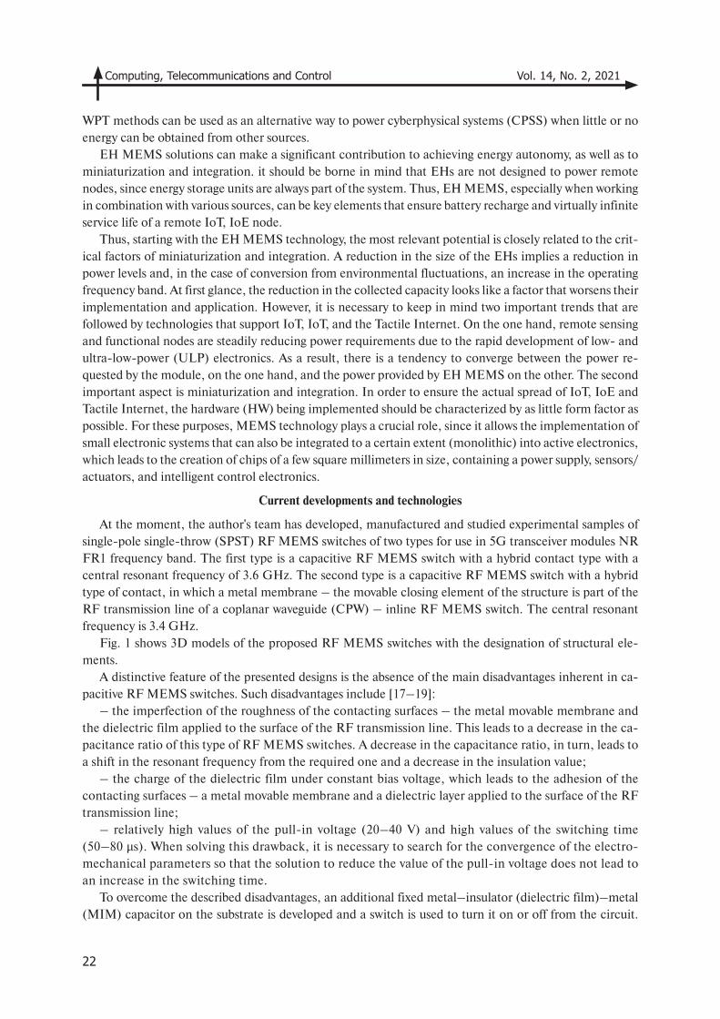
At the moment, the author's team has developed, manufactured and studied experimental samples of single-pole single-throw (SPST) RF MEMS switches of two types for use in 5G transceiver modules NR FR1 frequency band. The first type is a capacitive RF MEMS switch with a hybrid contact type with a central resonant frequency of 3.6 GHz. The second type is a capacitive RF MEMS switch with a hybrid type of contact, in which a metal membrane – the movable closing element of the structure is part of the RF transmission line of a coplanar waveguide (CPW) – inline RF MEMS switch. The central resonant frequency is 3.4 GHz.
Fig. 1 shows 3D models of the proposed RF MEMS switches with the designation of structural ele-ments.
A distinctive feature of the presented designs is the absence of the main disadvantages inherent in ca-pacitive RF MEMS switches. Such disadvantages include [17–19]:
– the imperfection of the roughness of the contacting surfaces – the metal movable membrane and the dielectric film applied to the surface of the RF transmission line. This leads to a decrease in the ca-pacitance ratio of this type of RF MEMS switches. A decrease in the capacitance ratio, in turn, leads to a shift in the resonant frequency from the required one and a decrease in the insulation value;
– the charge of the dielectric film under constant bias voltage, which leads to the adhesion of the contacting surfaces – a metal movable membrane and a dielectric layer applied to the surface of the RF transmission line;
– relatively high values of the pull-in voltage (20–40 V) and high values of the switching time (50–80 μs). When solving this drawback, it is necessary to search for the convergence of the electro-mechanical parameters so that the solution to reduce the value of the pull-in voltage does not lead to an increase in the switching time.
To overcome the described disadvantages, an additional fixed metal–insulator (dielectric film)–metal (MIM) capacitor on the substrate is developed and a switch is used to turn it on or off from the circuit.
I.E. Lysenko, A.V. Tkachenko, DOI: 10.18721/JCSTCS.14202
23
This results in a capacitance ratio that is independent of the roughness of the contacting surfaces and is therefore ideal for dielectrics with high permittivity and roughness. The material of the dielectric film of the additional fixed MIM capacitor is a dielectric material with a high permittivity of high-k dielectrics. Additional fixed MIM capacitor is connected to a shunt capacitor with metal-air-metal (MAM) plates formed by the upper metal film of the MIM capacitor, a metal movable membrane, and an air space be-tween them. The MIM capacitor is connected to the MAM capacitor in series, in the case when the metal movable membrane is in the up-position (open-state). In the case when the metal movable membrane is in the down-position (close-state), the MAM capacitor changes to the resistance in the electrical circuit. At the same time, such disadvantages of these designs as the high geometric dimensions of the metal movable membrane, as well as the high contact resistance introduced by the metal movable membrane in the closed state of the switch, are excluded [20].
The small value of the pull-in voltage and the short switching time is achieved by using four elastic sus-pensions having a zig-zag shape, a small air gap between the metal movable membrane and the fixed down actuation electrodes, a small thickness of the membrane, as well as the choice of the material of the mova-ble structures using the developed method of material selection in the design of RF MEMS switches [21].
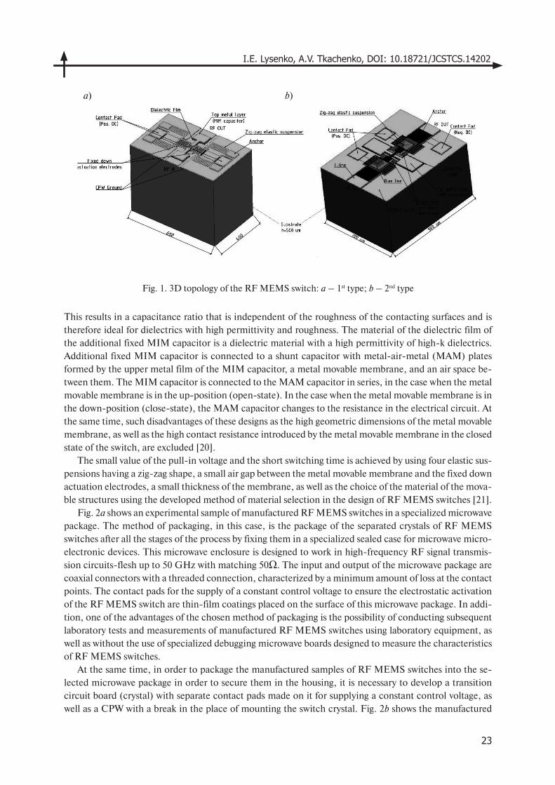
Fig. 2a shows an experimental sample of manufactured RF MEMS switches in a specialized microwave package. The method of packaging, in this case, is the package of the separated crystals of RF MEMS switches after all the stages of the process by fixing them in a specialized sealed case for microwave micro-electronic devices. This microwave enclosure is designed to work in high-frequency RF signal transmis-sion circuits-flesh up to 50 GHz with matching 50Ω. The input and output of the microwave package are coaxial connectors with a threaded connection, characterized by a minimum amount of loss at the contact points. The contact pads for the supply of a constant control voltage to ensure the electrostatic activation of the RF MEMS switch are thin-film coatings placed on the surface of this microwave package. In addi-tion, one of the advantages of the chosen method of packaging is the possibility of conducting subsequent laboratory tests and measurements of manufactured RF MEMS switches using laboratory equipment, as well as without the use of specialized debugging microwave boards designed to measure the characteristics of RF MEMS switches.
At the same time, in order to package the manufactured samples of RF MEMS switches into the se-lected microwave package in order to secure them in the housing, it is necessary to develop a transition circuit board (crystal) with separate contact pads made on it for supplying a constant control voltage, as well as a CPW with a break in the place of mounting the switch crystal. Fig. 2b shows the manufactured
a) b)
Fig. 1. 3D topology of the RF MEMS switch: a – 1st type; b – 2nd type
Computing, Telecommunications and Control Vol. 14, No. 2, 2021
24
Fig. 2. Manufactured experimental samples of RF MEMS switches:
a – in a specialized microwave package; b – experimental sample of manufactured adapter boards
adapter boards. Installation of the RF MEMS switch crystal is carried out by placing it in a pre-centered and etched groove in the adapter board and gluing it with polyimide glue.
The connection of the CPW of the adapter board with the CPW located on the RF MEMS switch crys-tal is carried out by a gold wire (d = 40 μm) using a micro-welding operation. The connection of the con-tact pads of the microwave housing-adapter board-crystal RF MEMS switch for the supply of a constant control voltage is also carried out with a gold wire (d = 20 μm) using a micro-welding operation.
Table 1 shows the extended results of laboratory tests of experimental samples of RF MEMS switches.
Table 1Results of laboratory tests
SPST RF MEMS switch@ 3.6 GHz, S-band
SPST RF MEMS switch @ 3,4 GHz, L, S, C, X-band
Effective frequency range S Effective frequency
range L, S, C, X
Insertion loss(open-state) –0.07 dB @ 3.6 GHz Insertion loss
(open-state) –0.18 dB @ 3.4 GHz
Isolation (close-state) –44.2 dB @ 3.6 GHz Isolation (close-state) –55.2 dB @ 3.4 GHz
Contact resistance Less 1 Ω Contact resistance Less 1 ΩLinearity High Linearity High
Power consumption Less 1 μW Power consumption Less 1 μW
Bias Voltage 3.5 V Bias Voltage 2 V
Pull-in Voltage Less 10 V Pull-in Voltage Less 10 V
Switching time ~ 10 μs Switching time ~ 10 μs
Switching power More 1 W Switching power More 1 W
Sensitivity to external mechanical influences High Sensitivity to external
mechanical influences High
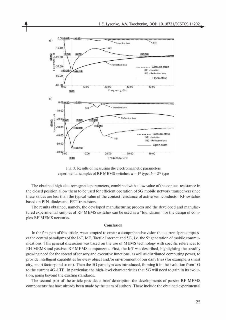
Fig. 3 shows the experimental results of measuring the electromagnetic parameters (scattering parameters) of the manufactured experimental samples of RF MEMS switches.
a) b)
I.E. Lysenko, A.V. Tkachenko, DOI: 10.18721/JCSTCS.14202
25
Fig. 3. Results of measuring the electromagnetic parameters
experimental samples of RF MEMS switches: a – 1st type; b – 2nd type
The obtained high electromagnetic parameters, combined with a low value of the contact resistance in the closed position allow them to be used for efficient operation of 5G mobile network transceivers since these values are less than the typical value of the contact resistance of active semiconductor RF switches based on PIN-diodes and FET-transistors.
The results obtained, namely, the developed manufacturing process and the developed and manufac-tured experimental samples of RF MEMS switches can be used as a “foundation” for the design of com-plex RF MEMS networks.
Conclusion
In the first part of this article, we attempted to create a comprehensive vision that currently encompass-es the central paradigms of the IoT, IoE, Tactile Internet and 5G, i.e. the 5th generation of mobile commu-nications. This general discussion was based on the use of MEMS technology with specific references to EH MEMS and passives RF MEMS components. First, the IoT was described, highlighting the steadily growing need for the spread of sensory and executive functions, as well as distributed computing power, to provide intelligent capabilities for every object and/or environment of our daily lives (for example, a smart city, smart factory and so on). Then the 5G paradigm was introduced, framing it in the evolution from 1G to the current 4G-LTE. In particular, the high-level characteristics that 5G will need to gain in its evolu-tion, going beyond the existing standards.
The second part of the article provides a brief description the developments of passive RF MEMS components that have already been made by the team of authors. These include the obtained experimental
a)
b)
Frequency, GHz
Frequency, GHz
S-pa
ram
eter
s, d
BS-
para
met
ers,
dB
Computing, Telecommunications and Control Vol. 14, No. 2, 2021
26
REFERENCES
1. Larson L.E., Hackett R.H., Melendes M.A., Lohr R.F. Micromachined microwave actuator (MIMAC)
technology – a new tuning approach for microwave integrated circuits. Proceedings of the IEEE Microwave and
Millimeter-Wave Monolithic Circuits Symposium, 1991, Pp. 27–30.
2. Goldsmith C., Lin T.-H., Powers B., Wu W.-R., Norvell B. Micromechanical membrane switches for
microwave applications. Proceedings of the IEEE MTT-S International Microwave Symposium, 1995, Vol. 1,
Pp. 91–94.
3. Goldsmith C., Randall J., Eshelman S., Lin T.-H., Denniston D., Chen S., Norvell B. Characteristics of
micromachined switches at microwave frequencies. Proceedings of the IEEE MTT-S International Microwave
Symposium, 1996, Vol. 2, Pp. 1141–1144.
4. Liu C. Foundations of MEMS. 2nd edition, Pearson Education, London, 2011.
5. Lee H.S., Leung C.H., Shi J., Chan S.C. Micro-electro-mechanical relays design concepts and process
demonstrations. Proceedings the 50th IEEE Holm Conference on Electrical Contacts and the 22nd International
Conference on Electrical Contacts, 2004, Pp. 242–247.
6. Cho I.-J., Song T., Baek S.-H., Yoon E. A low-voltage and low-power RF MEMS series and shunt switch-
es actuated by combination of electromagnetic and electrostatic forces. IEEE Trans. on Microwave Theory and
Technology, 2005, Vol. 53, Pp. 2450–2457.
7. Safari A., Akdogan E.K. Piezoelectric and acoustic materials for transducer applications. 1st edition, Spring-
er, New York, 2008.
8. Daneshmand M., Fouladi S., Mansour R.R., Lisi M., Stajcer T. Thermally-actuated latching RF MEMS
switch. Proceeding IEEE Int. Microwave Symposium MTT-S, 2009, Pp. 1217–1220.
9. Iannacci J. Practical guide to RF MEMS. 1st edition, Wiley VCH, Weinheim, 2013.
10. Nguyen C.T.-C. Transceiver front-end architectures using vibrating micromechanical signal processors. Top-
ical meeting on silicon monolithic integrated circuits in RF systems. 2001, Pp. 23–32.
11. Gammel P., Pehlke D.R., Brunel D., Kovacic S.J., Walsh K. 5G in perspective: a pragmatic guide to
what’s next [Skyworks]. Available: https://www.skyworksinc.com/-/media/skyworks/documents/products/2701-
2800/5g-white-paper.pdf (Accessed 15.06.2021).
12. Sohraby K., Minoli D., Znati T. Wireless sensor networks: Technology, protocols, and applications. 1st edi-
tion, John Wiley & Sons, Hoboken, 2007.
13. Kázmierski T.J., Beeby S. Energy harvesting systems: principles. Modeling and Applications. 1st edition,
Springer Verlag, New York, 2010.
14. Fu H., Yeatman E.M. Broadband rotational energy harvesting using bistable mechanism and frequency
up-conversion. Proceeding IEEE MEMS, 2017, Pp. 853–856.
15. Zhang Y., Luo A., Xu Y., Wang T., Wang F. Wideband MEMS electrostatic energy harvester with dual
resonant structure. Proceeding IEEE Sensors, 2016, Pp. 1–3.
samples of SPST capacitive RF MEMS switches with hybrid contact type for use in 5G NR FR1 mobile network transceivers. Further plans for the development of this work are the development of wafer-level packaging solutions at the plate level with the technology of through silicon vias (TSV) for the redistribu-tion of the electrical signal from passive devices in the package – RF MEMS to the outside world. As well as the development of RF MEMS switches to a different frequency range 5G – NR FR2 in one or more directions (SPnT).
Acknowledgments
The work was funded by Federal budget, task No. FENW-2020-0022 for the implementation of sci-entific research on “Development and research of methods and means of monitoring, diagnostics and forecasting state of engineering objects based on artificial intelligence”.
I.E. Lysenko, A.V. Tkachenko, DOI: 10.18721/JCSTCS.14202
27
16. Ghafouri N., Kim H., Atashbar M.Z., Najafi K. A micro thermoelectric energy scavenger for a hybrid
insect. Proceeding IEEE Sensors, 2008, Pp. 1249–1252.
17. Lysenko I.E., Tkachenko A.V., Sherova E.V., Nikitin A.V. Analytical approach in the development of RF
MEMS switches. Electronics, 2018, Vol. 7, No. 12, Pp. 1–23.
18. Lysenko I.E., Tkachenko A.V., Ezhova O.A., Konoplev B.G., Ryndin E.A., Sherova E.V. The mechanical
effects influencing on the design of RF MEMS switches. Electronics, 2020, Vol. 9, No. 2, Pp. 1–26.
19. Tkachenko A.V., Lysenko I.E. High capacitance ratio radio-frequency micromechanical switch. Prob-
lems of Advanced Micro- and Nanoelectronic Systems Development, 2020, Vol. 3, Pp. 237–243. (rus)
20. Lysenko I.E., Tkachenko A.V., Ezhova O.A., Naymenko D.V. Designing high-performance radio-fre-
quency micromechanical switches. Nanoindustriya, 2020, Vol. 13, No. S5-2 (102), Pp. 527–541. (rus). DOI:
10.221-84/1993-8578.2020.13.5s.527.541
21. Lysenko I.E., Tkachenko A.V., Ezhova O.A. Research of the microelectromechanical switch with dif-
ferent materials of metal membrane. Proceedings of SPIE 11022, International Conference on Micro- and Nano-
Electronics, 2018, Vol. 10226, Pp. 1–12.
Received 29.05.2021.
СПИСОК ЛИТЕРАТУРЫ
1. Larson L.E., Hackett R.H., Melendes M.A., Lohr R.F. Micromachined microwave actuator (MIMAC)
technology – a new tuning approach for microwave integrated circuits // Proc. of the IEEE Microwave and
Millimeter-Wave Monolithic Circuits Symp. 1991. Pp. 27–30.
2. Goldsmith C., Lin T.-H., Powers B., Wu W.-R., Norvell B. Micromechanical membrane switches for mi-
crowave applications // Proc. of the IEEE MTT-S Internat. Microwave Symp. 1995. Vol. 1. Pp. 91–94.
3. Goldsmith C., Randall J., Eshelman S., Lin T.-H., Denniston D., Chen S., Norvell B. Characteristics of
micromachined switches at microwave frequencies // Proc. of the IEEE MTT-S Internat. Microwave Symp.
1996. Vol. 2. Pp. 1141–1144.
4. Liu C. Foundations of MEMS. 2nd ed. London: Pearson Education, 2011.
5. Lee H.S., Leung C.H., Shi J., Chan S.C. Micro-electro-mechanical relays design concepts and process
demonstrations // Proc. the 50th IEEE Holm Conf. on Electrical Contacts and the 22nd Internat. Conf. on Elec-
trical Contacts. 2004. Pp. 242–247.
6. Cho I.-J., Song T., Baek S.-H., Yoon E. A low-voltage and low-power RF MEMS series and shunt switch-
es actuated by combination of electromagnetic and electrostatic forces // IEEE Trans. on Microwave Theory
and Technology. 2005. Vol. 53. Pp. 2450–2457.
7. Safari A., Akdogan E.K. Piezoelectric and acoustic materials for transducer applications. 1st ed. New York:
Springer, 2008.
8. Daneshmand M., Fouladi S., Mansour R.R., Lisi M., Stajcer T. Thermally-actuated latching RF MEMS
switch // Proc. IEEE Int. Microwave Symp. MTT-S. 2009. Pp. 1217–1220.
9. Iannacci J. Practical guide to RF MEMS. 1st ed. Wiley VCH, Weinheim, 2013.
10. Nguyen C.T.-C. Transceiver front-end architectures using vibrating micromechanical signal processors.
Topical meeting on silicon monolithic integrated circuits in RF systems. 2001. Pp. 23–32.
11. Gammel P., Pehlke D.R., Brunel D., Kovacic S.J., Walsh K. 5G in perspective: a pragmatic guide to
what’s next [Skyworks] // URL: https://www.skyworksinc.com/-/media/skyworks/documents/products/2701-
2800/5g-white-paper.pdf (Дата обращения: 15.06.2021).
12. Sohraby K., Minoli D., Znati T. Wireless sensor networks: Technology, protocols, and applications. 1st ed.
Hoboken: John Wiley & Sons, 2007.
13. Kázmierski T.J., Beeby S. Energy harvesting systems: principles. Modeling and Applications. 1st ed. New
York: Springer Verlag, 2010.
Computing, Telecommunications and Control Vol. 14, No. 2, 2021
28
14. Fu H., Yeatman E.M. Broadband rotational energy harvesting using bistable mechanism and frequency
up-conversion // Proc. IEEE MEMS. 2017. Pp. 853–856.
15. Zhang Y., Luo A., Xu Y., Wang T., Wang F. Wideband MEMS electrostatic energy harvester with dual
resonant structure // Proc. IEEE Sensors. 2016. Pp. 1–3.
16. Ghafouri N., Kim H., Atashbar M.Z., Najafi K. A micro thermoelectric energy scavenger for a hybrid
insect // Proc. IEEE Sensors. 2008. Pp.1249–1252.
17. Lysenko I.E., Tkachenko A.V., Sherova E.V., Nikitin A.V. Analytical approach in the development of RF
MEMS switches // Electronics. 2018. Vol. 7. No. 12. Pp. 1–23.
18. Lysenko I.E., Tkachenko A.V., Ezhova O.A., Konoplev B.G., Ryndin E.A., Sherova E.V. The mechanical
effects influencing on the design of RF MEMS switches // Electronics. 2020. Vol. 9. No. 2. Pp. 1–26.
19. Ткаченко А.В., Лысенко И.Е. Радиочастотный микромеханический переключатель с высоким от-
ношением емкости // Problems of Advanced Micro- and Nanoelectronic Systems Development. 2020. Vol. 3.
Pp. 237–243. DOI: 10.31114/2078-7707-2020-3-237-243
20. Лысенко И.Е., Ткаченко А.В., Ежова O.A., Науменко Д.В. Проектирование высокопроизводи-
тельных радиочастотных микромеханических переключателей // Наноиндустрия. Спецвыпуск. 2020.
Т. 13. S5-2 (102). С. 527–541. DOI: 10.22184/1993-8578.2020.13.5s.527.541
21. Lysenko I.E., Tkachenko A.V., Ezhova O.A. Research of the microelectromechanical switch with differ-
ent materials of metal membrane // Proc. of SPIE 11022, Internat. Conf. on Micro- and Nano-Electronics.
2018. Vol. 10226. Pp. 1–12.
Статья поступила в редакцию 29.05.2021.
THE AUTHORS / СВЕДЕНИЯ ОБ АВТОРАХ
Lysenko Igor E.Лысенко Игорь ЕвгеньевичE-mail: [email protected]
Tkachenko Alexey V.Ткаченко Алексей ВячеславовичE-mail: [email protected]
© Санкт-Петербургский политехнический университет Петра Великого, 2021
E.V. Zavorotneva, D.A. Indeitsev, A.V. Lukin, et al., DOI: 10.18721/JCSTCS.14203
29
DOI: 10.18721/JCSTCS.14203УДК 681.5.01
TECHNIQUE FOR COMPACT MODELING OF THERMOELECTRIC SYSTEMS
E.V. Zavorotneva, D.A. Indeitsev, A.V. Lukin, I.A. Popov, P.P. Udalov
Peter the Great St. Petersburg Polytechnic University,St. Petersburg, Russian Federation
This article describes a technique for modeling a thermoelectric module (TEM) based on a systematic approach using compact models. A finite-element model of a Peltier battery was built in the COMSOL software environment. A numerical analysis of the characteristics of TEM in the case of the dependence of material parameters on temperature is carried out. A compact dynamic TEM model has been constructed and verified on the basis of direct numerical modeling of a number of stationary and non-stationary problems for TEM. The presented approach facilitates the modeling of a thermoelectric module and its interrelationships with control units and other thermal elements under various boundary and initial conditions. The simulation results are in good agreement with the results obtained using other models described in the literature, as well as with numerical solutions. Based on numerical experiments, it is noted that the dependence of the physical parameters of the Peltier battery on temperature can distort the output parameters of the TEM and, if possible, should be taken into account in a compact model.
Keywords: thermoelectric module, system reduction, compact model, Matlab, COMSOL, sssMOR.
Citation: Zavorotneva E.V., Indeitsev D.A., Lukin A.V., Popov I.A., Udalov P.P. Technique for compact modeling of thermoelectric systems. Computing, Telecommunications and Control, 2021, Vol. 14, No. 2, Pp. 29–48. DOI: 10.18721/JCST-CS.14203
This is an open access article under the CC BY-NC 4.0 license (https://creativecommons.org/licenses/by-nc/4.0/).
МЕТОДИКА КОМПАКТНОГО МОДЕЛИРОВАНИЯ ТЕРМОЭЛЕКТРИЧЕСКИХ СИСТЕМ
Е.В. Заворотнева, Д.А. Индейцев, А.В. Лукин, И.А. Попов, П.П. Удалов
Санкт-Петербургский политехнический университет Петра Великого,Санкт-Петербург, Российская Федерация
Описана методика моделирования термоэлектрического модуля (ТЭМ) на базе си-стемного подхода с применением компактных моделей. Построена конечно-элементная модель батареи Пельтье в программной среде COMSOL. Проведен численный анализ ха-рактеристик ТЭМ в случае зависимости материальных параметров от температуры. Вы-полнено построение компактной динамической модели ТЭМ и её верификация на осно-ве прямого численного моделирования ряда стационарных и нестационарных задач для ТЭМ. Представленный подход облегчает моделирование термоэлектрического модуля и его взаимосвязей с блоками управления и другими тепловыми элементами при различ-ных граничных и начальных условиях. Результаты моделирования хорошо согласуются с результатами, полученными с использованием других моделей, описанных в литературе, а также с численными решениями. Отмечено, что зависимость физических параметров
Computing, Telecommunications and Control Vol. 14, No. 2, 2021
30
батареи Пельтье от температуры может искажать выходные параметры ТЭМ и по возмож-ности должна быть учтена в компактной модели.
Ключевые слова: термоэлектрический модуль, редуцирование систем, компактная модель, Matlab, COMSOL, sssMOR.
Ссылка при цитировании: Zavorotneva E.V., Indeitsev D.A., Lukin A.V., Popov I.A., Udalov P.P. Technique for compact modeling of thermoelectric systems // Computing, Telecommunications and Control. 2021. Vol. 14. No. 2. Pp. 29–48. DOI: 10.18721/JCSTCS.14203
Cтатья открытого доступа, распространяемая по лицензии CC BY-NC 4.0 (https://creative-commons.org/licenses/by-nc/4.0/).
Introduction
There are several techniques for thermoelectric process modeling. The first method consists in standard finite element modeling using well-known packages such as COMSOL, ANSYS [1–3]. The second meth-od is based on the numerical integration of differential equations using platforms such as MATLAB Sim-ulink [4, 5]. The third method is based on the construction of equivalent electrical circuits in the SPICE, PSPICE software packages [6–9].
Thermoelectric modules are used in cases where it is impossible to use classical methods or principles of thermostating, which are based on the use of refrigerants, and when active cooling or power generation is required. The field of application of thermoelectric devices is extremely large. Thermoelectric modules are used in solid-state and diode lasers, telecommunications equipment, electronics, various equipment in transport, spacecraft, and also in everyday life. One of the promising directions for the development and application of thermoelectric systems is the development of thermoelectric devices based on microelec-tromechanical systems (MEMS), which can be used to stabilize the temperature of various high-precision sensors [10, 11]. With the growth of requirements for the performance of microsystem technology, there is a fundamental need for the development of cooling systems for electronic devices. The purpose of this work is to develop a methodology for compact computationally efficient modeling of controlled thermo- electric processes in distributed systems.
Modern numerical tools make it easy to obtain solutions to various physical problems, but a single calculation is not always able to meet the design needs. A way out of this situation is to synthesize ap-proximation models based on direct numerical modeling, which are much simpler in further analysis. It is convenient to combine compact models of individual parts of the system into a single system model of the object under study in Simulink or ANSYS TwinBuilder analysis systems, given that the general view of nonlinearities and the type of converters are not so convenient and clear in direct software implementation at the script level. The construction diagram of the proposed compact model of the thermostating system is shown in the Fig. 1.
Construction order includes the following steps: 1. For the control object and all components of the thermostating system, except for the Peltier ele-
ments, a finite element model is built. The computational domain is obtained considering the construction of a denser mesh in places with large thermal gradients, in close proximity to areas of application of ther-mal loads and near objects of interest from the point of view of the simulation model.
2. The resulting finite element model using the finite element analysis system is uploaded in vec-tor-matrix form to the Matlab software system.
3. On the basis of global matrices, a system in the state space is built and reduced, while the inputs of the model are heat fluxes on the pads of thermoelectric modules and all external loads, and the outputs are the temperatures of sites and those nodes in which the thermal field is of greatest interest. For relatively small models, it is possible to use the built-in functions of the Matlab system (Control System Toolbox). For large models, it is recommended to use the sssMOR methods, which are described in detail in [12].
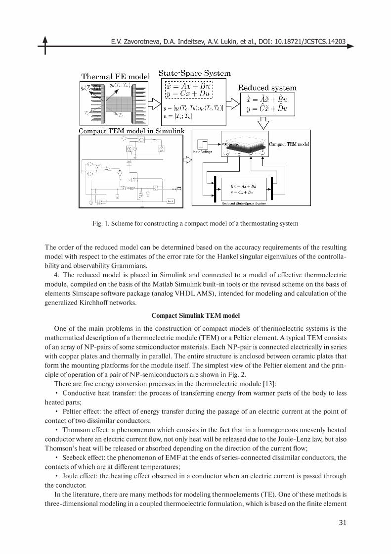
E.V. Zavorotneva, D.A. Indeitsev, A.V. Lukin, et al., DOI: 10.18721/JCSTCS.14203
31
Fig. 1. Scheme for constructing a compact model of a thermostating system
The order of the reduced model can be determined based on the accuracy requirements of the resulting model with respect to the estimates of the error rate for the Hankel singular eigenvalues of the controlla-bility and observability Grammians.
4. The reduced model is placed in Simulink and connected to a model of effective thermoelectric module, compiled on the basis of the Matlab Simulink built-in tools or the revised scheme on the basis of elements Simscape software package (analog VHDL AMS), intended for modeling and calculation of the generalized Kirchhoff networks.
Compact Simulink TEM model
One of the main problems in the construction of compact models of thermoelectric systems is the mathematical description of a thermoelectric module (TEM) or a Peltier element. A typical TEM consists of an array of NP-pairs of some semiconductor materials. Each NP-pair is connected electrically in series with copper plates and thermally in parallel. The entire structure is enclosed between ceramic plates that form the mounting platforms for the module itself. The simplest view of the Peltier element and the prin-ciple of operation of a pair of NP-semiconductors are shown in Fig. 2.
There are five energy conversion processes in the thermoelectric module [13]:• Conductive heat transfer: the process of transferring energy from warmer parts of the body to less
heated parts;• Peltier effect: the effect of energy transfer during the passage of an electric current at the point of
contact of two dissimilar conductors;• Thomson effect: a phenomenon which consists in the fact that in a homogeneous unevenly heated
conductor where an electric current flow, not only heat will be released due to the Joule-Lenz law, but also Thomson’s heat will be released or absorbed depending on the direction of the current flow;
• Seebeck effect: the phenomenon of EMF at the ends of series-connected dissimilar conductors, the contacts of which are at different temperatures;
• Joule effect: the heating effect observed in a conductor when an electric current is passed through the conductor.
In the literature, there are many methods for modeling thermoelements (TE). One of these methods is three-dimensional modeling in a coupled thermoelectric formulation, which is based on the finite element
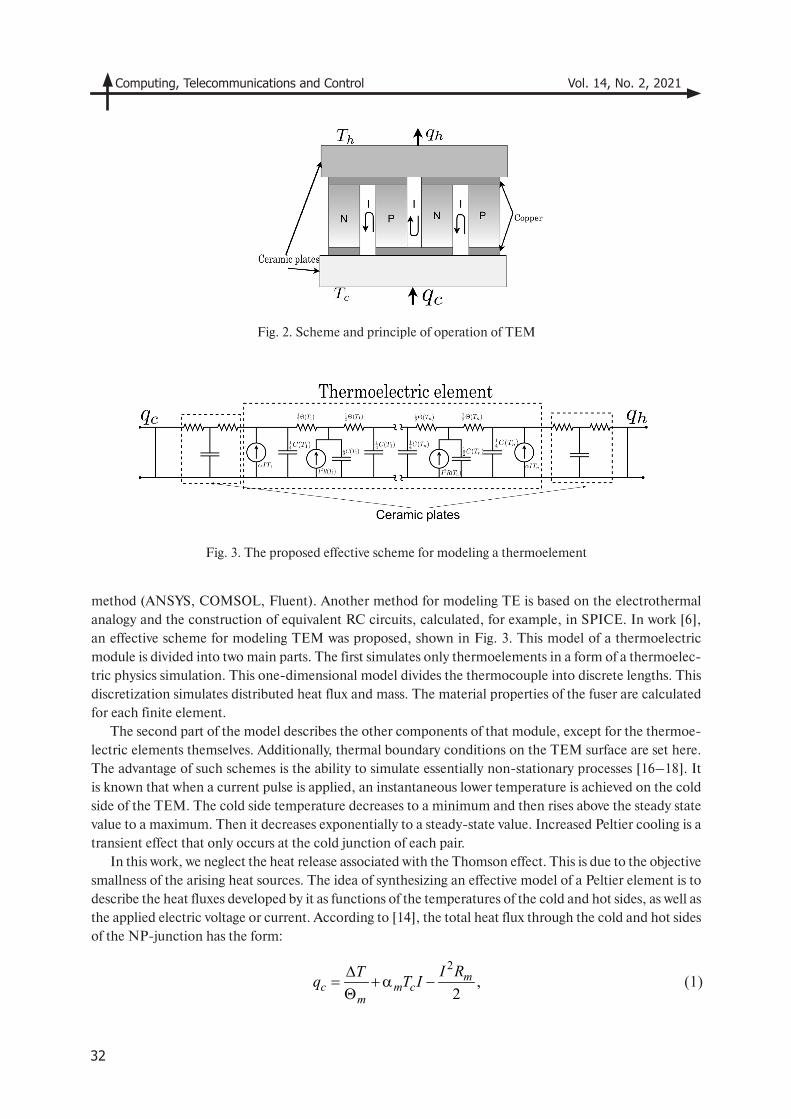
Computing, Telecommunications and Control Vol. 14, No. 2, 2021
32
Fig. 2. Scheme and principle of operation of TEM
Fig. 3. The proposed effective scheme for modeling a thermoelement
method (ANSYS, COMSOL, Fluent). Another method for modeling TE is based on the electrothermal analogy and the construction of equivalent RC circuits, calculated, for example, in SPICE. In work [6], an effective scheme for modeling TEM was proposed, shown in Fig. 3. This model of a thermoelectric module is divided into two main parts. The first simulates only thermoelements in a form of a thermoelec-tric physics simulation. This one-dimensional model divides the thermocouple into discrete lengths. This discretization simulates distributed heat flux and mass. The material properties of the fuser are calculated for each finite element.
The second part of the model describes the other components of that module, except for the thermoe-lectric elements themselves. Additionally, thermal boundary conditions on the TEM surface are set here. The advantage of such schemes is the ability to simulate essentially non-stationary processes [16–18]. It is known that when a current pulse is applied, an instantaneous lower temperature is achieved on the cold side of the TEM. The cold side temperature decreases to a minimum and then rises above the steady state value to a maximum. Then it decreases exponentially to a steady-state value. Increased Peltier cooling is a transient effect that only occurs at the cold junction of each pair.
In this work, we neglect the heat release associated with the Thomson effect. This is due to the objective smallness of the arising heat sources. The idea of synthesizing an effective model of a Peltier element is to describe the heat fluxes developed by it as functions of the temperatures of the cold and hot sides, as well as the applied electric voltage or current. According to [14], the total heat flux through the cold and hot sides of the NP-junction has the form:
2,
2m
c m cm
I RTq T I∆= +α −Θ
(1)
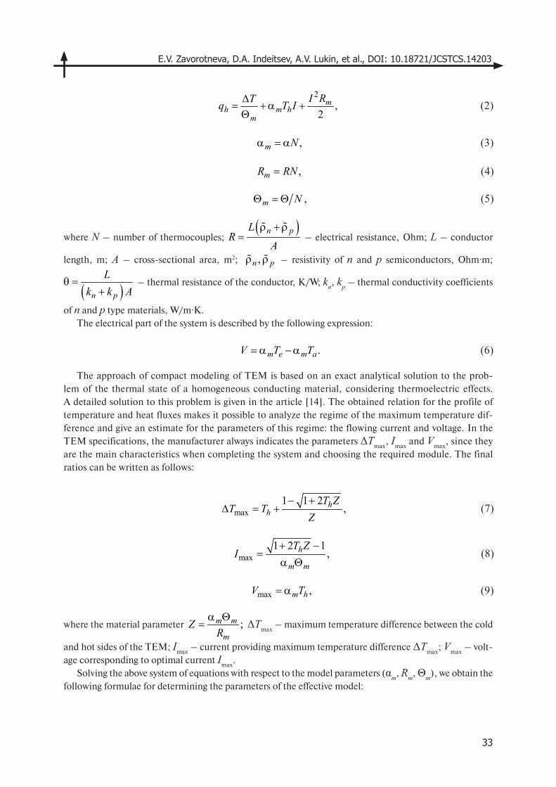
E.V. Zavorotneva, D.A. Indeitsev, A.V. Lukin, et al., DOI: 10.18721/JCSTCS.14203
33
where N – number of thermocouples; – electrical resistance, Ohm; L – conductor
length, m; A – cross-sectional area, m2; – resistivity of n and p semiconductors, Ohm∙m;
– thermal resistance of the conductor, K/W; kn, kp – thermal conductivity coefficients
of n and p type materials, W/m∙K. The electrical part of the system is described by the following expression:
The approach of compact modeling of TEM is based on an exact analytical solution to the prob-lem of the thermal state of a homogeneous conducting material, considering thermoelectric effects. A detailed solution to this problem is given in the article [14]. The obtained relation for the profile of temperature and heat fluxes makes it possible to analyze the regime of the maximum temperature dif-ference and give an estimate for the parameters of this regime: the flowing current and voltage. In the TEM specifications, the manufacturer always indicates the parameters ΔTmax, Imax and Vmax, since they are the main characteristics when completing the system and choosing the required module. The final ratios can be written as follows:
where the material parameter ΔTmax – maximum temperature difference between the cold
and hot sides of the TEM; Imax – current providing maximum temperature difference ΔTmax; Vmax – volt-age corresponding to optimal current Imax.
Solving the above system of equations with respect to the model parameters (αm, Rm, Θm), we obtain the following formulae for determining the parameters of the effective model:
(2)2
,2
mh m h
m
I RTq T I∆= +α +Θ
,m Nα = α (3)
,mR RN= (4)
,m NΘ = Θ (5)
( )n pLR
A
ρ +ρ=
,n pρ ρ
( )n p
Lk k A
θ =+
.m e m aV T T= α −α (6)
max1 1 2
,hh
T ZT T
Z− +
∆ = + (7)
max1 2 1
,h
m m
T ZI
+ −=
α Θ(8)
max ,m hV T= α (9)
;m m
mZ
Rα Θ
=
Computing, Telecommunications and Control Vol. 14, No. 2, 2021
34
Since the calculated material parameters are the characteristics of the entire module, and to build an effective TEM model, the parameters of each individual element are required, it is necessary to calculate these parameters using the manufacturer’s database. Following the web-site of the manufacturer Kryo-therm [15], a universal abbreviation of the type TB-N-C-h is used for the names of single-stage modules. TB stands for thermoelectric battery (module); N is the number of thermoelectric pairs in the module; C is the length of the edge of the base of the thermoelectric element (in millimeters); h is the height of the ther-moelectric element (in millimeters). The manufacturer also provides information on the dimensions of the thermoelectric module, namely the total height of the module and the width of the ceramic plates. The material of ceramic plates in standard delivery conditions is Al
2O
3 ceramics. Material properties for copper
conductors in TEM can be neglected due to their relatively small size. This means that using the obtained generalized material properties of TEM and knowing the properties of the material and the geometry of ceramic insulators, one can find the necessary parameters for constructing the RC TEM model. The total thermal resistance will now be the sum of two terms, the first is responsible for thermoelectric elements, the second is for ceramic plates. In this case, the effective Seebeck coefficient and electrical resistance do not need to be divided into components, since these effects occur only in a thermoelectric element and have no relation to ceramics:
The thermal resistance of a ceramic plate can be calculated using the formula for the thermal resistance of a section of a constant section circuit:
where l – thermal circuit length, m; λ – material thermal conductivity coefficient, W/(m∙K); S – cross-sectional area of a site, m2.
Thermoelements in TEM have parallel resistance, which means that the thermal resistance of one thermoelement is calculated as:
where N – number of thermocouples in TEM.The value for electrical resistance and the Seebeck coefficient are calculated similarly:
( ) [ ]max max
max,h
mh
V T TR
I T−∆
= Ω (10)
(11)( )max
max max max
2 K ,W
hm
h
T TI V T T
∆ Θ = − ∆
max V .Km
h
VT
α = (12)
K .Wm te c Θ = Θ +Θ
(13)
K ,Wc
lS Θ = λ
(14)
( ) K2 2 ,WN m cN Θ = Θ − Θ
(15)
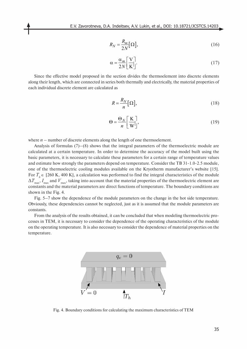
E.V. Zavorotneva, D.A. Indeitsev, A.V. Lukin, et al., DOI: 10.18721/JCSTCS.14203
35
Since the effective model proposed in the section divides the thermoelement into discrete elements along their length, which are connected in series both thermally and electrically, the material properties of each individual discrete element are calculated as
where n – number of discrete elements along the length of one thermoelement. Analysis of formulas (7)–(8) shows that the integral parameters of the thermoelectric module are
calculated at a certain temperature. In order to determine the accuracy of the model built using the basic parameters, it is necessary to calculate these parameters for a certain range of temperature values and estimate how strongly the parameters depend on temperature. Consider the TB 31-1.0-2.5 module, one of the thermoelectric cooling modules available on the Kryotherm manufacturer’s website [15]. For Th ∈ [260 K, 400 K], a calculation was performed to find the integral characteristics of the module ΔTmax, Imax and Vmax, taking into account that the material properties of the thermoelectric element are constants and the material parameters are direct functions of temperature. The boundary conditions are shown in the Fig. 4.
Fig. 5–7 show the dependence of the module parameters on the change in the hot side temperature. Obviously, these dependencies cannot be neglected, just as it is assumed that the module parameters are constants.
From the analysis of the results obtained, it can be concluded that when modeling thermoelectric pro-cesses in TEM, it is necessary to consider the dependence of the operating characteristics of the module on the operating temperature. It is also necessary to consider the dependence of material properties on the temperature.
[ ],2
mN
RRN
= Ω (16)
V .2 K
mN
α α = (17)
[ ],NRRn
= Ω (18)
K ,W
NnΘ Θ =
(19)
Fig. 4. Boundary conditions for calculating the maximum characteristics of TEM
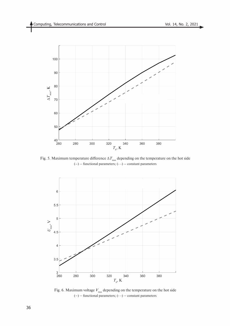
Computing, Telecommunications and Control Vol. 14, No. 2, 2021
36
Fig. 5. Maximum temperature difference ΔTmax
depending on the temperature on the hot side
(–) – functional parameters; (- -) – constant parameters
Fig. 6. Maximum voltage Vmax
depending on the temperature on the hot side
(–) – functional parameters; (- -) – constant parameters
Th, K
ΔTm
ax, K
Th, K
Um
ax, V
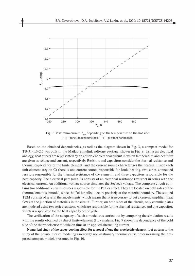
E.V. Zavorotneva, D.A. Indeitsev, A.V. Lukin, et al., DOI: 10.18721/JCSTCS.14203
37
Fig. 7. Maximum current Imax
depending on the temperature on the hot side
(–) – functional parameters; (- -) – constant parameters
Based on the obtained dependencies, as well as the diagram shown in Fig. 3, a compact model for TB-31-1.0-2.5 was built in the Matlab Simulink software package, shown in Fig. 8. Using an electrical analogy, heat effects are represented by an equivalent electrical circuit in which temperature and heat flux are given as voltage and current, respectively. Resistors and capacitors consider the thermal resistance and thermal capacitance of the finite element, and the current source characterizes the heating. Inside each unit element (region C) there is one current source responsible for Joule heating, two series-connected resistors responsible for the thermal resistance of the element, and three capacitors responsible for the heat capacity. The electrical part (area B) consists of an electrical resistance (resistor) in series with the electrical current. An additional voltage source simulates the Seebeck voltage. The complete circuit con-tains two additional current sources responsible for the Peltier effect. They are located on both sides of the thermoelement submodel, since the Peltier effect occurs precisely at the material boundary. The studied TEM consists of several thermoelements, which means that it is necessary to put a current amplifier (heat flow) at the junction of materials in the circuit. Further, on both sides of the circuit, only ceramic plates are modeled using two series resistors, which are responsible for the thermal resistance, and one capacitor, which is responsible for the heat capacity of the plate.
The verification of the adequacy of such a model was carried out by comparing the simulation results with the results obtained by direct finite-element (FE) analysis. Fig. 9 shows the dependence of the cold side of the thermoelectric module on time at an applied alternating current.
Numerical study of the super-cooling effect for a model of one thermoelectric element. Let us turn to the study of the possibilities of modeling essentially non-stationary thermoelectric processes using the pro-posed compact model, presented in Fig. 10.
Th, K
I max
, Am
p
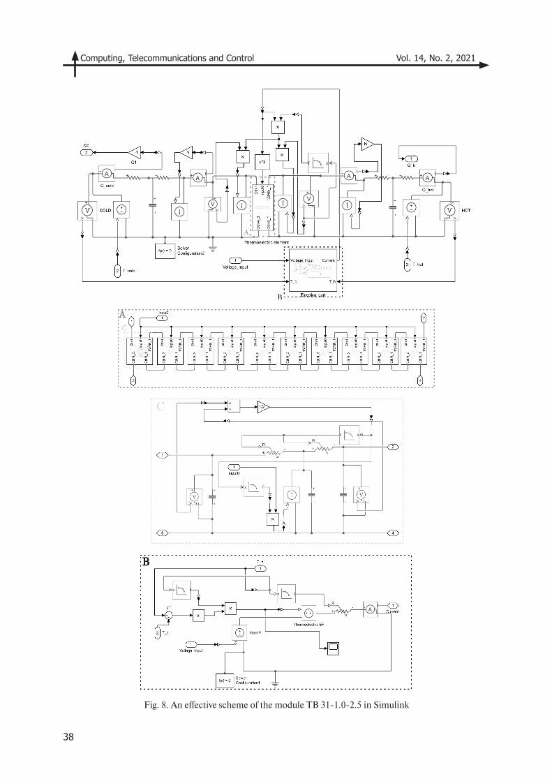
Computing, Telecommunications and Control Vol. 14, No. 2, 2021
38
Fig. 8. An effective scheme of the module TB 31-1.0-2.5 in Simulink
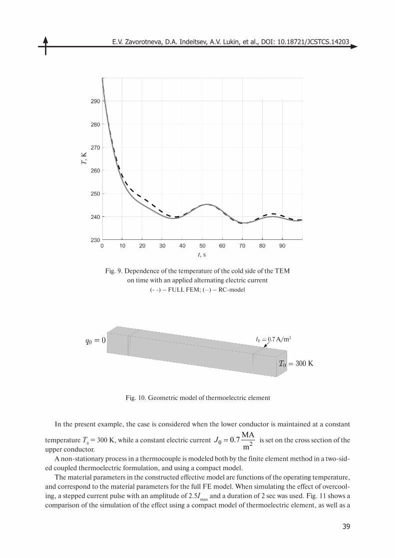
E.V. Zavorotneva, D.A. Indeitsev, A.V. Lukin, et al., DOI: 10.18721/JCSTCS.14203
39
In the present example, the case is considered when the lower conductor is maintained at a constant
temperature T0 = 300 K, while a constant electric current is set on the cross section of the
upper conductor.A non-stationary process in a thermocouple is modeled both by the finite element method in a two-sid-
ed coupled thermoelectric formulation, and using a compact model.The material parameters in the constructed effective model are functions of the operating temperature,
and correspond to the material parameters for the full FE model. When simulating the effect of overcool-ing, a stepped current pulse with an amplitude of 2.5Imax and a duration of 2 sec was used. Fig. 11 shows a comparison of the simulation of the effect using a compact model of thermoelectric element, as well as a
t, s
T, K
K
A/m2
0 2MA0.7m
J =
Fig. 10. Geometric model of thermoelectric element
Fig. 9. Dependence of the temperature of the cold side of the TEM
on time with an applied alternating electric current
(- -) – FULL FEM; (–) – RC-model
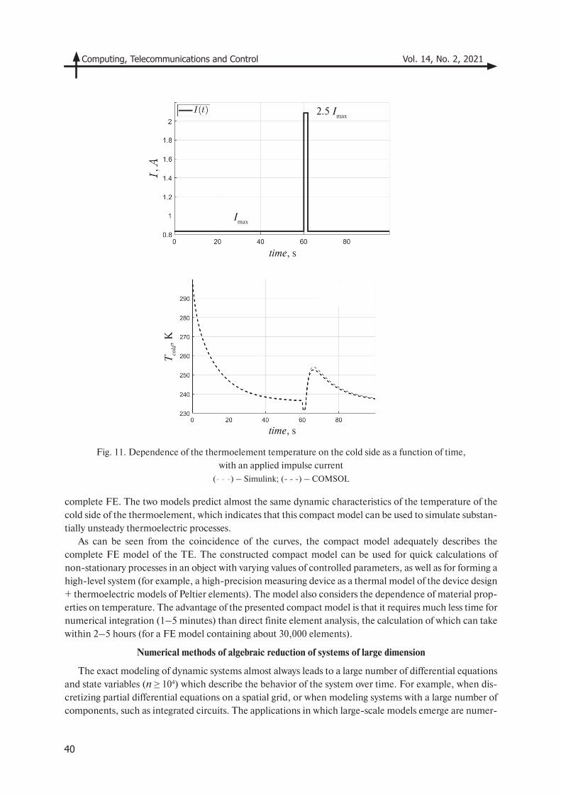
Computing, Telecommunications and Control Vol. 14, No. 2, 2021
40
Fig. 11. Dependence of the thermoelement temperature on the cold side as a function of time,
with an applied impulse current
(- - -) – Simulink; (- - -) – COMSOL
complete FE. The two models predict almost the same dynamic characteristics of the temperature of the cold side of the thermoelement, which indicates that this compact model can be used to simulate substan-tially unsteady thermoelectric processes.
As can be seen from the coincidence of the curves, the compact model adequately describes the complete FE model of the TE. The constructed compact model can be used for quick calculations of non-stationary processes in an object with varying values of controlled parameters, as well as for forming a high-level system (for example, a high-precision measuring device as a thermal model of the device design + thermoelectric models of Peltier elements). The model also considers the dependence of material prop-erties on temperature. The advantage of the presented compact model is that it requires much less time for numerical integration (1–5 minutes) than direct finite element analysis, the calculation of which can take within 2–5 hours (for a FE model containing about 30,000 elements).
Numerical methods of algebraic reduction of systems of large dimension
The exact modeling of dynamic systems almost always leads to a large number of differential equations and state variables (n ≥ 104) which describe the behavior of the system over time. For example, when dis-cretizing partial differential equations on a spatial grid, or when modeling systems with a large number of components, such as integrated circuits. The applications in which large-scale models emerge are numer-
2.5 Imax
Imax
time, s
Tco
ld, K
time, s
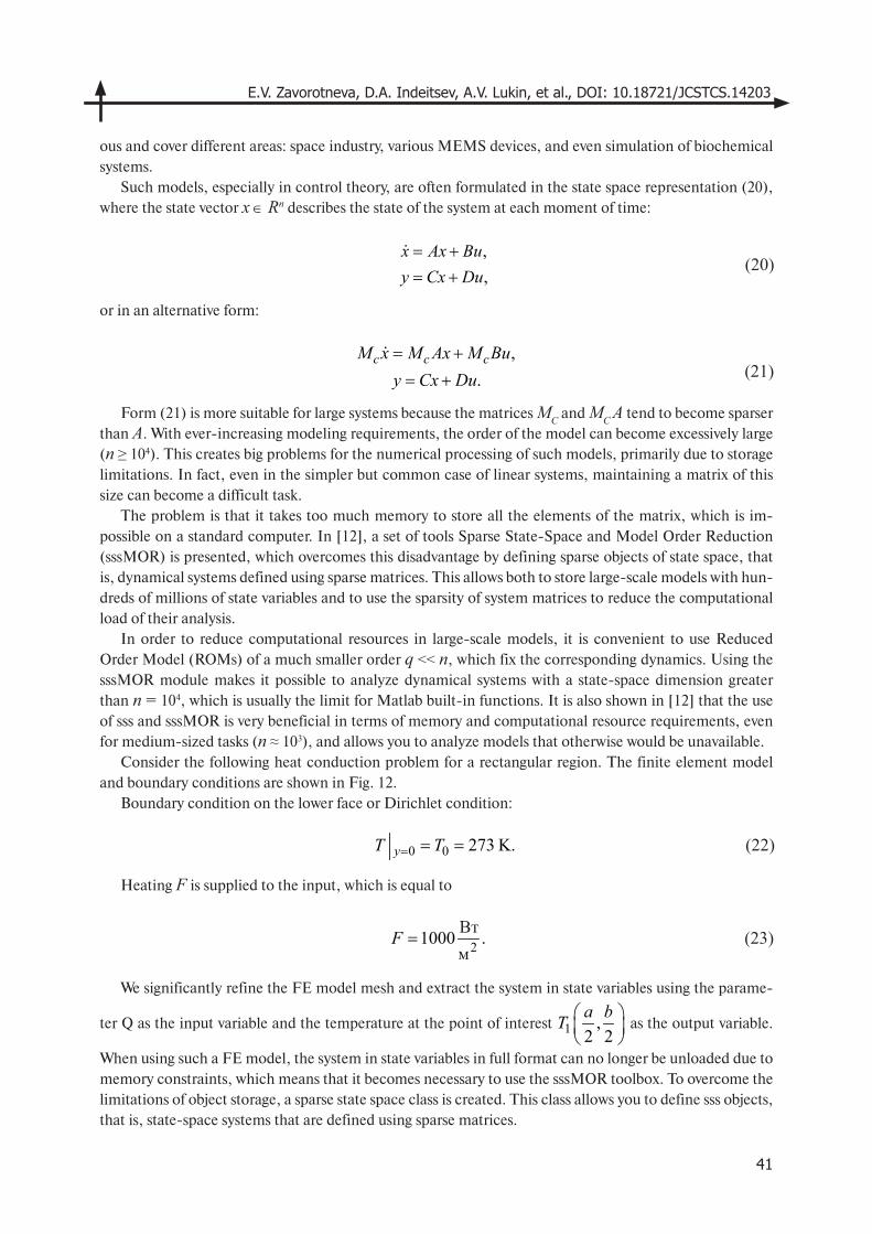
E.V. Zavorotneva, D.A. Indeitsev, A.V. Lukin, et al., DOI: 10.18721/JCSTCS.14203
41
ous and cover different areas: space industry, various MEMS devices, and even simulation of biochemical systems.
Such models, especially in control theory, are often formulated in the state space representation (20), where the state vector x ∈ Rn describes the state of the system at each moment of time:
or in an alternative form:
Form (21) is more suitable for large systems because the matrices MC and MC A tend to become sparser than A. With ever-increasing modeling requirements, the order of the model can become excessively large (n ≥ 104). This creates big problems for the numerical processing of such models, primarily due to storage limitations. In fact, even in the simpler but common case of linear systems, maintaining a matrix of this size can become a difficult task.
The problem is that it takes too much memory to store all the elements of the matrix, which is im-possible on a standard computer. In [12], a set of tools Sparse State-Space and Model Order Reduction (sssMOR) is presented, which overcomes this disadvantage by defining sparse objects of state space, that is, dynamical systems defined using sparse matrices. This allows both to store large-scale models with hun-dreds of millions of state variables and to use the sparsity of system matrices to reduce the computational load of their analysis.
In order to reduce computational resources in large-scale models, it is convenient to use Reduced Order Model (ROMs) of a much smaller order q << n, which fix the corresponding dynamics. Using the sssMOR module makes it possible to analyze dynamical systems with a state-space dimension greater than n = 104, which is usually the limit for Matlab built-in functions. It is also shown in [12] that the use of sss and sssMOR is very beneficial in terms of memory and computational resource requirements, even for medium-sized tasks (n ≈ 103), and allows you to analyze models that otherwise would be unavailable.
Consider the following heat conduction problem for a rectangular region. The finite element model and boundary conditions are shown in Fig. 12.
Boundary condition on the lower face or Dirichlet condition:
Heating F is supplied to the input, which is equal to
We significantly refine the FE model mesh and extract the system in state variables using the parame-
ter Q as the input variable and the temperature at the point of interest as the output variable.
When using such a FE model, the system in state variables in full format can no longer be unloaded due to memory constraints, which means that it becomes necessary to use the sssMOR toolbox. To overcome the limitations of object storage, a sparse state space class is created. This class allows you to define sss objects, that is, state-space systems that are defined using sparse matrices.
,,
x Ax Buy Cx Du= += +
(20)
,.
c c cM x M Ax M Buy Cx Du= +
= +
(21)
0 0 273 K.yT T= = = (22)
2Âò1000 .ì
F =Втм
(23)
1 ,2 2a bT
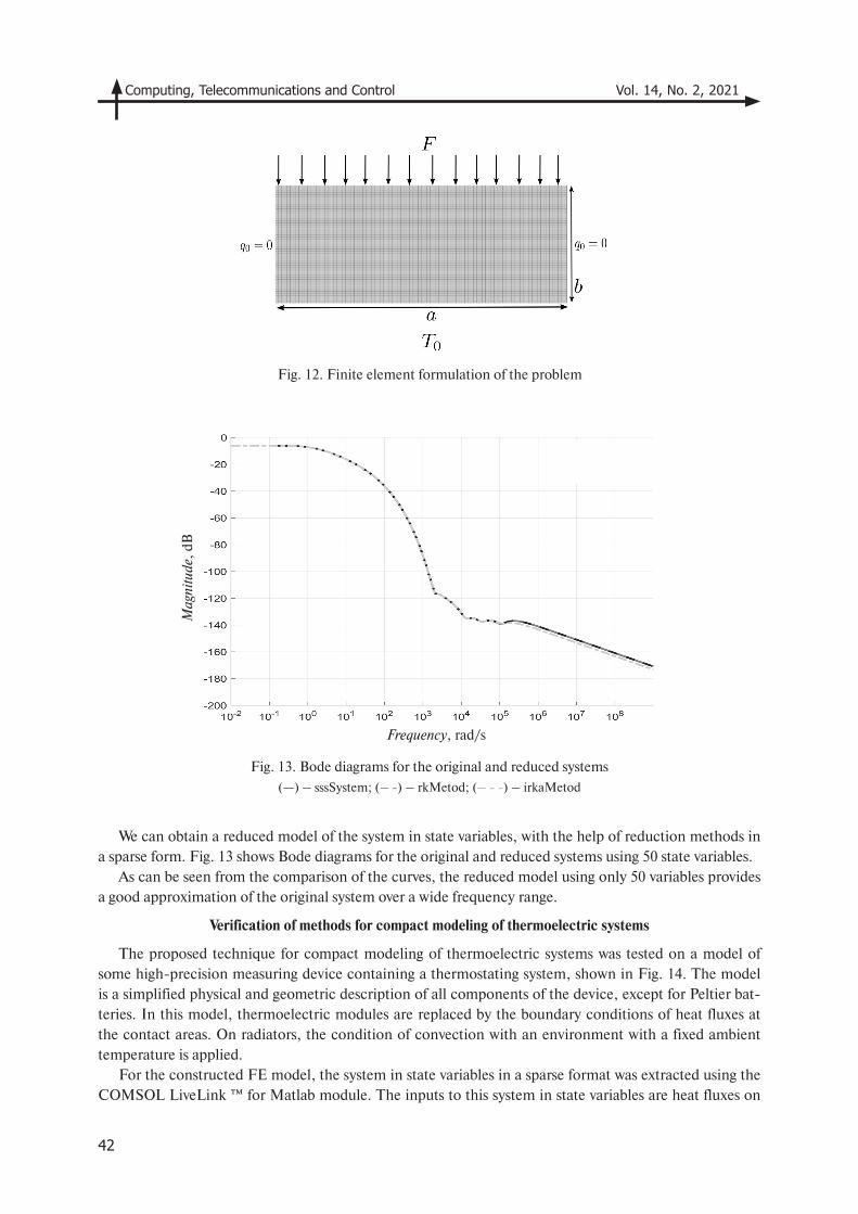
Computing, Telecommunications and Control Vol. 14, No. 2, 2021
42
Fig. 12. Finite element formulation of the problem
Fig. 13. Bode diagrams for the original and reduced systems
(—) – sssSystem; (– -) – rkMetod; (– - -) – irkaMetod
We can obtain a reduced model of the system in state variables, with the help of reduction methods in a sparse form. Fig. 13 shows Bode diagrams for the original and reduced systems using 50 state variables.
As can be seen from the comparison of the curves, the reduced model using only 50 variables provides a good approximation of the original system over a wide frequency range.
Verification of methods for compact modeling of thermoelectric systems
The proposed technique for compact modeling of thermoelectric systems was tested on a model of some high-precision measuring device containing a thermostating system, shown in Fig. 14. The model is a simplified physical and geometric description of all components of the device, except for Peltier bat-teries. In this model, thermoelectric modules are replaced by the boundary conditions of heat fluxes at the contact areas. On radiators, the condition of convection with an environment with a fixed ambient temperature is applied.
For the constructed FE model, the system in state variables in a sparse format was extracted using the COMSOL LiveLink ™ for Matlab module. The inputs to this system in state variables are heat fluxes on
Frequency, rad/s
Mag
nitu
de, d
B
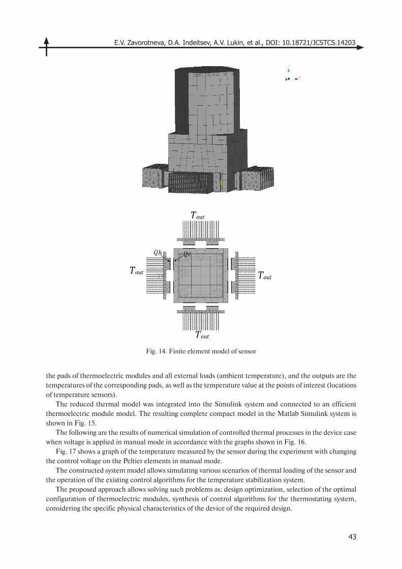
E.V. Zavorotneva, D.A. Indeitsev, A.V. Lukin, et al., DOI: 10.18721/JCSTCS.14203
43
the pads of thermoelectric modules and all external loads (ambient temperature), and the outputs are the temperatures of the corresponding pads, as well as the temperature value at the points of interest (locations of temperature sensors).
The reduced thermal model was integrated into the Simulink system and connected to an efficient thermoelectric module model. The resulting complete compact model in the Matlab Simulink system is shown in Fig. 15.
The following are the results of numerical simulation of controlled thermal processes in the device case when voltage is applied in manual mode in accordance with the graphs shown in Fig. 16.
Fig. 17 shows a graph of the temperature measured by the sensor during the experiment with changing the control voltage on the Peltier elements in manual mode.
The constructed system model allows simulating various scenarios of thermal loading of the sensor and the operation of the existing control algorithms for the temperature stabilization system.
The proposed approach allows solving such problems as: design optimization, selection of the optimal configuration of thermoelectric modules, synthesis of control algorithms for the thermostating system, considering the specific physical characteristics of the device of the required design.
Fig. 14. Finite element model of sensor
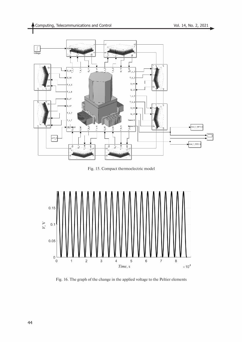
Computing, Telecommunications and Control Vol. 14, No. 2, 2021
44
Fig. 15. Compact thermoelectric model
Fig. 16. The graph of the change in the applied voltage to the Peltier elements
Time, s
V, V
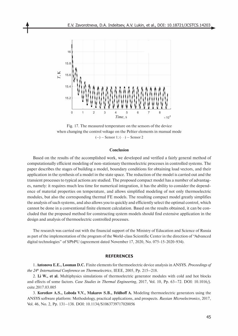
E.V. Zavorotneva, D.A. Indeitsev, A.V. Lukin, et al., DOI: 10.18721/JCSTCS.14203
45
REFERENCES
1. Antonova E.E., Looman D.C. Finite elements for thermoelectric device analysis in ANSYS. Proceedings of
the 24th International Conference on Thermoelectrics, IEEE, 2005, Pp. 215–218.
2. Li W., et al. Multiphysics simulations of thermoelectric generator modules with cold and hot blocks
and effects of some factors. Case Studies in Thermal Engineering, 2017, Vol. 10, Pp. 63–72. DOI: 10.1016/j.
csite.2017.03.005
3. Korotkov A.S., Loboda V.V., Makarov S.B., Feldhoff A. Modeling thermoelectric generators using the
ANSYS software platform: Methodology, practical applications, and prospects. Russian Microelectronics, 2017,
Vol. 46, No. 2, Pp. 131–138. DOI: 10.1134/S1063739717020056
Fig. 17. The measured temperature on the sensors of the device
when changing the control voltage on the Peltier elements in manual mode
(–) – Sensor 1; (- -) – Sensor 2
Conclusion
Based on the results of the accomplished work, we developed and verified a fairly general method of computationally efficient modeling of non-stationary thermoelectric processes in controlled systems. The paper describes the stages of building a model, boundary conditions for obtaining load vectors, and their application in the synthesis of a model in the state space. The reduction of the model is carried out and the transient processes to typical actions are studied. The proposed compact model has a number of advantag-es, namely: it requires much less time for numerical integration, it has the ability to consider the depend-ence of material properties on temperature, and allows simplified modeling of not only thermoelectric modules, but also the corresponding thermal FE models. The resulting compact model greatly simplifies the analysis of such systems, and also allows you to quickly and efficiently select the optimal control, which cannot be done in a conventional finite element calculation. Based on the results obtained, it can be con-cluded that the proposed method for constructing system models should find extensive application in the design and analysis of thermoelectric controlled processes.
The research was carried out with the financial support of the Ministry of Education and Science of Russia
as part of the implementation of the program of the World-class Scientific Center in the direction of “Advanced
digital technologies” of SPbPU (agreement dated November 17, 2020, No. 075-15-2020-934).
Time, s
T, K
Computing, Telecommunications and Control Vol. 14, No. 2, 2021
46
4. Tsai H.L., Lin J.M. Model building and simulation of thermoelectric module using Matlab/Simulink.
Journal of Electronic Materials, 2010, Vol. 39, No. 9, P. 2105. DOI: 10.1007/s11664-009-0994-x
5. Kobbekaduwa K., Subasinghe N.D. Modelling and analysis of thermoelectric generation of materials using
Matlab/Simulink. International Journal of Energy and Power Engineering, 2016, Vol. 5, No. 3, Pp. 97–104.
6. Mitrani D., Salazar J., Turó A., García M.J. Transient distributed parameter electrical analogous model
of TE devices. Microelectronics Journal, 2009, Vol. 40, No. 9, Pp. 1406–1410. DOI:10.1016/j.mejo.2008.06.038
7. Piggott A. Detailed transient multiphysics model for fast and accurate design, simulation and optimiza-
tion of a thermoelectric generator (TEG) or thermal energy harvesting device. Journal of Electronic Materials,
2019, Vol. 48, No. 9, Pp. 5442–5452.
8. Lineykin S.B., Ben-Yaakov S. PSPICE-compatible equivalent circuit of thermoelectric cooler. Proceedings
of the 36th Power Electronics Specialists Conference, IEEE, 2005, Pp. 608–612. DOI: 10.1109/PESC.2005.1581688
9. Chavez J.A., et al. SPICE model of thermoelectric elements including thermal effects. Proceedings of the
17th IEEE Instrumentation and Measurement Technology Conference, IEEE, 2000, Vol. 2, Pp. 1019–1023.
10. Korotkov A.S., Loboda V., Dzyubanenko S.V., Bakulin E. Fabrication and testing of MEMS technol-
ogy based thermoelectric generator. Proceedings of the 7th Electronic System-Integration Technology Conference
(ESTC), IEEE, 2018, Pp. 1–4. DOI: 10.1109/ESTC.2018.8546445
11. Korotkov A.S., Loboda V.V. Simulation and design of thin-film thermoelectric generators. 2018 Inter-
national Symposium on Fundamentals of Electrical Engineering (ISFEE), IEEE, 2018, Pp. 1–4. DOI: 10.1109/
ISFEE.2018.8742452
12. Castagnotto A., Varona M.C., Jeschek L., Lohmann B. Sss & sssMOR: Analysis and reduction of large-
scale dynamic systems in MATLAB. At-Automatisierungstechnik, 2017, Vol. 65, No. 2, Pp. 134–150. DOI:
10.1515/auto-2016-0137
13. Kaganov M.A., Privin M.R. Thermoelectric heat pumps. Ripol Classic, 2013.
14. Seifert W., Ueltzen M., Müller E. One‐dimensional modelling of thermoelectric cooling. Physica Status
Solidi (a), 2002, Vol. 194, No. 1, Pp. 277–290.
15. Production of thermoelectric modules. Available: http://kryothermtec.com/ru/
16. Piggott A.J., Allen J.S. Peltier supercooling with isosceles current pulses: A response surface perspective.
ECS Journal of Solid State Science and Technology, 2017, Vol. 6, No. 3, P. N3045. DOI: 10.1149/2.0061703jss
17. Snyder G.J., et al. Supercooling of Peltier cooler using a current pulse. Journal of Applied Physics, 2002,
Vol. 92, No. 3, Pp. 1564–1569.
18. Lv Hao, Wang Xiao-Dong, Meng Jing-Hui, Wang Tian-Hu. Optimal pulse current shape for transient
supercooling of thermoelectric cooler. Energy, 2015, Vol. 83, Pp. 788–796. DOI: 10.1016/j.energy.2015.02.092
Received 17.06.2021.
СПИСОК ЛИТЕРАТУРЫ
1. Antonova E.E., Looman D.C. Finite elements for thermoelectric device analysis in ANSYS // Proc. of the
24th International. Conf. on Thermoelectrics. IEEE, 2005. Pp. 215–218.
2. Li W., et al. Multiphysics simulations of thermoelectric generator modules with cold and hot blocks and
effects of some factors // Case Studies in Thermal Engineering. 2017. Vol. 10. Pp. 63–72. DOI: 10.1016/j.
csite.2017.03.005
3. Korotkov A.S., Loboda V.V., Makarov S.B., Feldhoff A. Modeling thermoelectric generators using the
ANSYS software platform: Methodology, practical applications, and prospects // Russian Microelectronics.
2017. Vol. 46. No. 2. Pp. 131–138. DOI: 10.1134/S1063739717020056
4. Tsai H.L., Lin J.M. Model building and simulation of thermoelectric module using Matlab/Simulink //
J. of Electronic Materials. 2010. Vol. 39. No. 9. P. 2105. DOI: 10.1007/s11664-009-0994-x
E.V. Zavorotneva, D.A. Indeitsev, A.V. Lukin, et al., DOI: 10.18721/JCSTCS.14203
47
5. Kobbekaduwa K., Subasinghe N.D. Modelling and analysis of thermoelectric generation of materials using
Matlab/Simulink // Internat. J. of Energy and Power Engineering. 2016. Vol. 5. No. 3. Pp. 97–104.
6. Mitrani D., Salazar J., Turó A., García M.J. Transient distributed parameter electrical analogous model of
TE devices // Microelectronics Journal. 2009. Vol. 40. No. 9. Pp. 1406–1410. DOI:10.1016/j.mejo.2008.06.038
7. Piggott A. Detailed transient multiphysics model for fast and accurate design, simulation and optimi-
zation of a thermoelectric generator (TEG) or thermal energy harvesting device // J. of Electronic Materials.
2019. Vol. 48. No. 9. Pp. 5442–5452.
8. Lineykin S.B., Ben-Yaakov S. PSPICE-compatible equivalent circuit of thermoelectric cooler // Proc.
of the 36th Power Electronics Specialists Conf. IEEE, 2005. Pp. 608–612. DOI: 10.1109/PESC.2005.1581688
9. Chavez J.A., et al. SPICE model of thermoelectric elements including thermal effects // Proc. of the 17th
IEEE Instrumentation and Measurement Technology Conf. IEEE, 2000. Vol. 2. Pp. 1019–1023.
10. Korotkov A.S., Loboda V., Dzyubanenko S.V., Bakulin E. Fabrication and testing of MEMS technology
based thermoelectric generator // Proc. of the 7th Electronic System-Integration Technology Conf. IEEE. 2018.
Pp. 1–4. DOI: 10.1109/ESTC.2018.8546445
11. Korotkov A.S., Loboda V.V. Simulation and design of thin-film thermoelectric generators // 2018 In-
ternat. Symp. on Fundamentals of Electrical Engineering (ISFEE). IEEE, 2018. Pp. 1–4. DOI: 10.1109/IS-
FEE.2018.8742452
12. Castagnotto A., Varona M.C., Jeschek L., Lohmann B. Sss & sssMOR: Analysis and reduction of large-
scale dynamic systems in Matlab // At-Automatisierungstechnik. 2017. Vol. 65. No. 2. Pp. 134–150. DOI:
10.1515/auto-2016-0137
13. Kaganov M.A., Privin M.R. Thermoelectric heat pumps. Ripol Classic, 2013.
14. Seifert W., Ueltzen M., Müller E. One‐dimensional modelling of thermoelectric cooling // Physica Sta-
tus Solidi (a). 2002. Vol. 194. No. 1. Pp. 277–290.
15. Производство термоэлектрических модулей // URL: http://kryothermtec.com/ru/
16. Piggott A.J., Allen J.S. Peltier supercooling with isosceles current pulses: A response surface perspective
// ECS Journal of Solid State Science and Technology. 2017. Vol. 6. No. 3. P. N3045. DOI: 10.1149/2.0061703jss
17. Snyder G.J., et al. Supercooling of Peltier cooler using a current pulse // J. of Applied Physics. 2002.
Vol. 92. No. 3. Pp. 1564–1569.
18. Lv Hao, Wang Xiao-Dong, Meng Jing-Hui, Wang Tian-Hu. Optimal pulse current shape for transient su-
percooling of thermoelectric cooler // Energy. 2015. Vol. 83. Pp. 788–796. DOI: 10.1016/j.energy.2015.02.092
Статья поступила в редакцию 17.06.2021.
THE AUTHORS / СВЕДЕНИЯ ОБ АВТОРАХ
Zavorotneva Ekaterina V.Заворотнева Екатерина ВладимировнаE-mail: [email protected]
Indeitsev Dmitry A.Индейцев Дмитрий АнатольевичE-mail: [email protected]
Lukin Aleksei V.Лукин Алексей ВячеславовичE-mail: [email protected]
Popov Ivan A.Попов Иван АлексеевичE-mail: [email protected]

Computing, Telecommunications and Control Vol. 14, No. 2, 2021
48
© Санкт-Петербургский политехнический университет Петра Великого, 2021
Udalov Pavel P.Удалов Павел ПавловичE-mail: [email protected]
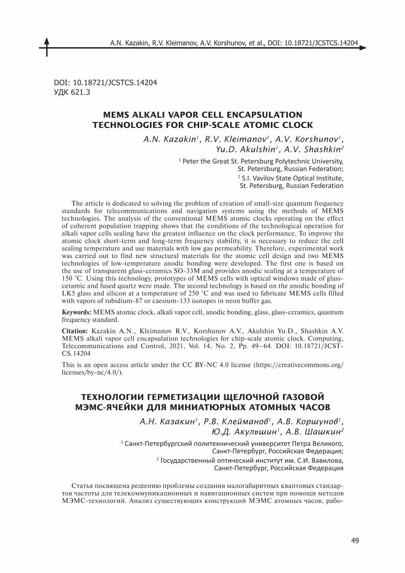
A.N. Kazakin, R.V. Kleimanov, A.V. Korshunov, et al., DOI: 10.18721/JCSTCS.14204
49
DOI: 10.18721/JCSTCS.14204УДК 621.3
MEMS ALKALI VAPOR CELL ENCAPSULATION TECHNOLOGIES FOR CHIP-SCALE ATOMIC CLOCK
A.N. Kazakin1, R.V. Kleimanov1, A.V. Korshunov1, Yu.D. Akulshin1, A.V. Shashkin2
1 Peter the Great St. Petersburg Polytechnic University,St. Petersburg, Russian Federation;2 S.I. Vavilov State Optical Institute,St. Petersburg, Russian Federation
The article is dedicated to solving the problem of creation of small-size quantum frequency standards for telecommunications and navigation systems using the methods of MEMS technologies. The analysis of the conventional MEMS atomic clocks operating on the effect of coherent population trapping shows that the conditions of the technological operation for alkali vapor cells sealing have the greatest influence on the clock performance. To improve the atomic clock short-term and long-term frequency stability, it is necessary to reduce the cell sealing temperature and use materials with low gas permeability. Therefore, experimental work was carried out to find new structural materials for the atomic cell design and two MEMS technologies of low-temperature anodic bonding were developed. The first one is based on the use of transparent glass-ceramics SO-33M and provides anodic sealing at a temperature of 150 °C. Using this technology, prototypes of MEMS cells with optical windows made of glass-ceramic and fused quartz were made. The second technology is based on the anodic bonding of LK5 glass and silicon at a temperature of 250 °C and was used to fabricate MEMS cells filled with vapors of rubidium-87 or caesium-133 isotopes in neon buffer gas.
Keywords: MEMS atomic clock, alkali vapor cell, anodic bonding, glass, glass-ceramics, quantum frequency standard.
Citation: Kazakin A.N., Kleimanov R.V., Korshunov A.V., Akulshin Yu.D., Shashkin A.V. MEMS alkali vapor cell encapsulation technologies for chip-scale atomic clock. Computing, Telecommunications and Control, 2021, Vol. 14, No. 2, Pp. 49–64. DOI: 10.18721/JCST-CS.14204
This is an open access article under the CC BY-NC 4.0 license (https://creativecommons.org/licenses/by-nc/4.0/).
ТЕХНОЛОГИИ ГЕРМЕТИЗАЦИИ ЩЕЛОЧНОЙ ГАЗОВОЙ МЭМС-ЯЧЕЙКИ ДЛЯ МИНИАТЮРНЫХ АТОМНЫХ ЧАСОВ
А.Н. Казакин1, Р.В. Клейманов1, А.В. Коршунов1, Ю.Д. Акульшин1, А.В. Шашкин2
1 Санкт-Петербургский политехнический университет Петра Великого,Санкт-Петербург, Российская Федерация;
2 Государственный оптический институт им. С.И. Вавилова,Санкт-Петербург, Российская Федерация
Статья посвящена решению проблемы создания малогабаритных квантовых стандар-тов частоты для телекоммуникационных и навигационных систем при помощи методов МЭМС-технологий. Анализ существующих конструкций МЭМС атомных часов, рабо-
Computing, Telecommunications and Control Vol. 14, No. 2, 2021
50
тающих на эффекте когерентного пленения населенностей, показал, что наибольшее влияние на их метрологические характеристики оказывают условия проведения опера-ции герметизации парощелочных атомных ячеек. Для повышения точности и долговре-менной стабильности МЭМС часов необходимо уменьшать температуру этой операции и применять материалы с низкой газопроницаемостью. Поэтому была проведена экспе-риментальная работа по поиску новых конструкционных материалов для атомной ячей-ки и разработаны две технологии низкотемпературной анодной термодиффузионной герметизации. Первая основана на применении прозрачной стеклокерамики СО-33М и позволяет проводить анодную герметизацию при температуре 150 °С. По этой техно-логии изготовлены прототипы МЭМС-ячеек с окнами из стеклокерамики и плавленого кварца. Вторая технология, основанная на анодном соединении стекла ЛК5 и кремния при 250 °С, использована для изготовления действующих образцов МЭМС-ячеек, за-полненных парами изотопов рубидия-87 или цезия-133 и буферным газом неоном.
Ключевые слова: МЭМС, атомные часы, щелочная ячейка, анодная сварка, стекло, стекло-керамика, квантовый стандарт частоты.
Ссылка при цитировании: Kazakin A.N., Kleimanov R.V., Korshunov A.V., Akulshin Yu.D., Shashkin A.V. MEMS alkali vapor cell encapsulation technologies for chip-scale atomic clock // Computing, Telecommunications and Control. 2021. Vol. 14. No. 2. Pp. 49–64. DOI: 10.18721/JCSTCS.14204
Cтатья открытого доступа, распространяемая по лицензии CC BY-NC 4.0 (https://creative-commons.org/licenses/by-nc/4.0/).
Introduction
The application fields of quantum devices with optical pumping is expanding every year: from telecom-munication, network synchronization and satellite navigation systems [1–3] to medical diagnostics [4], atomic spectroscopy [5] and quantum-enhanced metrology systems based on ensemble of ultra cold atoms [6]. The success achieved in the miniaturization of quantum devices and the development of standard-ized methods of physics packaging of optical component with electronics ensured their mass production [7–10]. Development of technologies of microelectromechanical systems (MEMS) and vertical-cavity surface-emitting lasers (VCSEL) made it possible to create miniature atomic magnetometers and chip-scale atomic clocks (CSAC) based on the coherent population trapping (CPT) effect [11–13].
A key element of modern quantum devices is millimeter-size atomic cells containing alkali metal vapors in inert atmosphere or vacuum [1, 14, 15]. To increase the atomic quality factor and reduce fre-quency instability of CSAC, different buffer gases or organic anti-relaxation coatings of the inner walls of the cell are used [16, 17]. Benefiting from planar MEMS technologies, MEMS cells are characterized by small size, flat optical windows, low fabricating cost, and provide low power consumption and sim-plicity of integration with other components of CSAC (thin film heaters, anti-reflective coatings, optical filters, microlens, etc.) [12].
The MEMS cells are formed by sandwiching a silicon wafer with through-hole cavity between two transparent glass wafers. The main processes of the MEMS cells technology are optical cavities forma-tion, filling with an alkali metal source and vacuum-tight sealing of the cell in the appropriate buffer atmosphere [18]. Optical cavities are implemented by dry or wet through-wafer etching of silicon. Pure alkali metals or alkali salts with reducing agent are used as vapors sources.
Vacuum-tight sealing is the main MEMS technology that has the greatest impact on the atomic cell performance. For hermetic sealing of such devices on a wafer level, various bonding technologies are used, the most widespread of which is the anodic bonding of silicon and glass wafers [19]. Anodic bond-ing is based on electro-chemical processes taking place between joined surfaces at elevated temperatures and under action of electric field [20]. Materials for the anodic bonding are special borosilicate glasses (Borofloat 33, Pyrex 7740), which have high ionic conductivity at bonding temperatures, optical trans-parency and coefficient of thermal expansion (CTE) approximately matched to CTE of silicon. At the
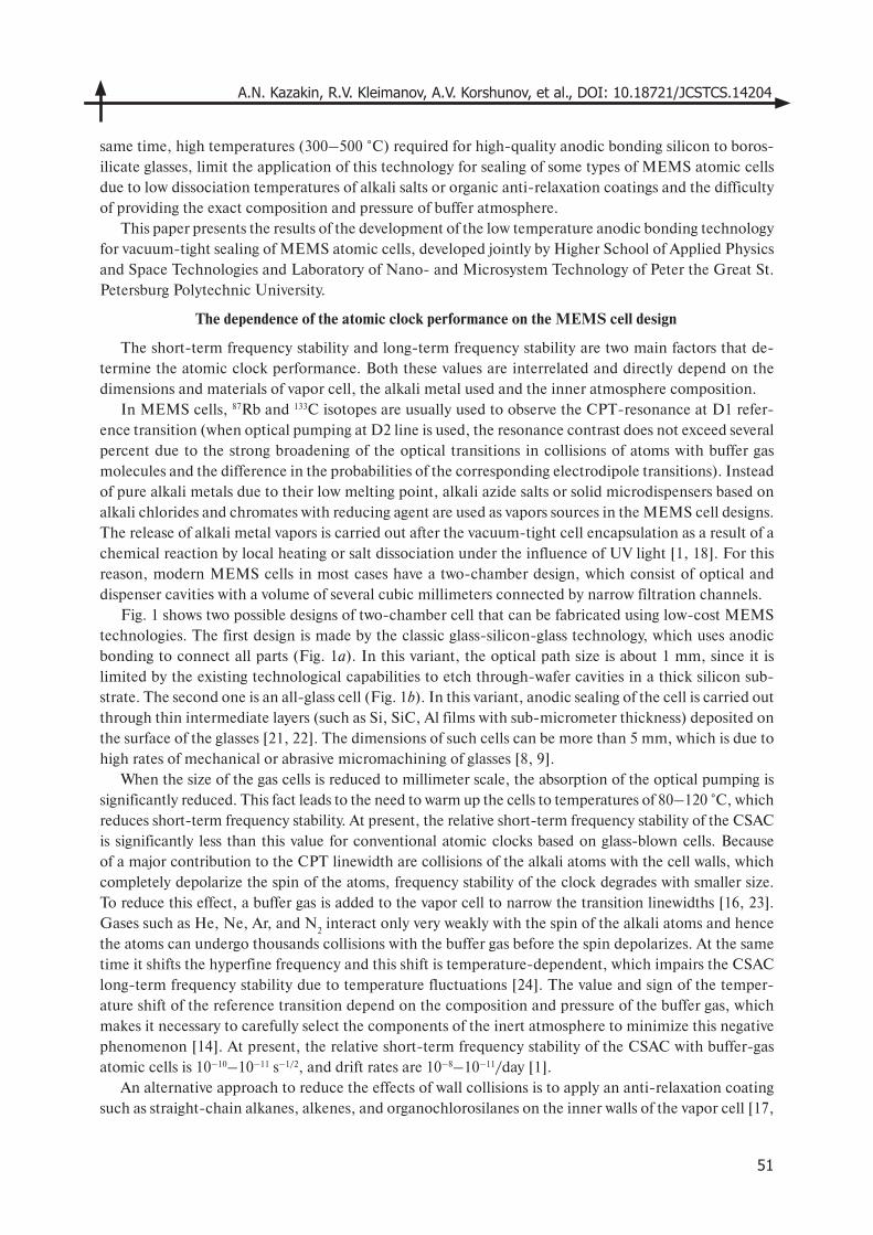
A.N. Kazakin, R.V. Kleimanov, A.V. Korshunov, et al., DOI: 10.18721/JCSTCS.14204
51
same time, high temperatures (300–500 °C) required for high-quality anodic bonding silicon to boros-ilicate glasses, limit the application of this technology for sealing of some types of MEMS atomic cells due to low dissociation temperatures of alkali salts or organic anti-relaxation coatings and the difficulty of providing the exact composition and pressure of buffer atmosphere.
This paper presents the results of the development of the low temperature anodic bonding technology for vacuum-tight sealing of MEMS atomic cells, developed jointly by Higher School of Applied Physics and Space Technologies and Laboratory of Nano- and Microsystem Technology of Peter the Great St. Petersburg Polytechnic University.
The dependence of the atomic clock performance on the MEMS cell design
The short-term frequency stability and long-term frequency stability are two main factors that de-termine the atomic clock performance. Both these values are interrelated and directly depend on the dimensions and materials of vapor cell, the alkali metal used and the inner atmosphere composition.
In MEMS cells, 87Rb and 133C isotopes are usually used to observe the CPT-resonance at D1 refer-ence transition (when optical pumping at D2 line is used, the resonance contrast does not exceed several percent due to the strong broadening of the optical transitions in collisions of atoms with buffer gas molecules and the difference in the probabilities of the corresponding electrodipole transitions). Instead of pure alkali metals due to their low melting point, alkali azide salts or solid microdispensers based on alkali chlorides and chromates with reducing agent are used as vapors sources in the MEMS cell designs. The release of alkali metal vapors is carried out after the vacuum-tight cell encapsulation as a result of a chemical reaction by local heating or salt dissociation under the influence of UV light [1, 18]. For this reason, modern MEMS cells in most cases have a two-chamber design, which consist of optical and dispenser cavities with a volume of several cubic millimeters connected by narrow filtration channels.
Fig. 1 shows two possible designs of two-chamber cell that can be fabricated using low-cost MEMS technologies. The first design is made by the classic glass-silicon-glass technology, which uses anodic bonding to connect all parts (Fig. 1a). In this variant, the optical path size is about 1 mm, since it is limited by the existing technological capabilities to etch through-wafer cavities in a thick silicon sub-strate. The second one is an all-glass cell (Fig. 1b). In this variant, anodic sealing of the cell is carried out through thin intermediate layers (such as Si, SiC, Al films with sub-micrometer thickness) deposited on the surface of the glasses [21, 22]. The dimensions of such cells can be more than 5 mm, which is due to high rates of mechanical or abrasive micromachining of glasses [8, 9].
When the size of the gas cells is reduced to millimeter scale, the absorption of the optical pumping is significantly reduced. This fact leads to the need to warm up the cells to temperatures of 80–120 °C, which reduces short-term frequency stability. At present, the relative short-term frequency stability of the CSAC is significantly less than this value for conventional atomic clocks based on glass-blown cells. Because of a major contribution to the CPT linewidth are collisions of the alkali atoms with the cell walls, which completely depolarize the spin of the atoms, frequency stability of the clock degrades with smaller size. To reduce this effect, a buffer gas is added to the vapor cell to narrow the transition linewidths [16, 23]. Gases such as He, Ne, Ar, and N
2 interact only very weakly with the spin of the alkali atoms and hence
the atoms can undergo thousands collisions with the buffer gas before the spin depolarizes. At the same time it shifts the hyperfine frequency and this shift is temperature-dependent, which impairs the CSAC long-term frequency stability due to temperature fluctuations [24]. The value and sign of the temper-ature shift of the reference transition depend on the composition and pressure of the buffer gas, which makes it necessary to carefully select the components of the inert atmosphere to minimize this negative phenomenon [14]. At present, the relative short-term frequency stability of the CSAC with buffer-gas atomic cells is 10–10–10–11 s–1/2, and drift rates are 10–8–10–11/day [1].
An alternative approach to reduce the effects of wall collisions is to apply an anti-relaxation coating such as straight-chain alkanes, alkenes, and organochlorosilanes on the inner walls of the vapor cell [17,
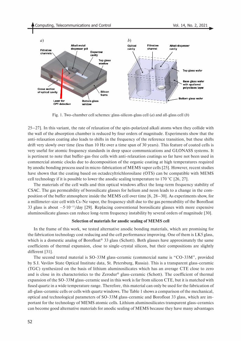
Computing, Telecommunications and Control Vol. 14, No. 2, 2021
52
Fig. 1. Two-chamber cell schemes: glass-silicon-glass cell (a) and all-glass cell (b)
25–27]. In this variant, the rate of relaxation of the spin-polarized alkali atoms when they collide with the wall of the absorption chamber is reduced by four orders of magnitude. Experiments show that the anti-relaxation coating also leads to shifts in the frequency of the reference transition, but these shifts drift very slowly over time (less than 10 Hz over a time span of 30 years). This feature of coated cells is very useful for atomic frequency standards in deep space communications and GLONASS systems. It is pertinent to note that buffer-gas-free cells with anti-relaxation coatings so far have not been used in commercial atomic clocks due to decomposition of the organic coating at high temperatures required by anodic bonding process used in micro-fabrication of MEMS vapor cells [25]. However, recent studies have shown that the coating based on octadecyltrichlorosilane (OTS) can be compatible with MEMS cell technology if it is possible to lower the anodic sealing temperature to 170 °C [26, 27].
The materials of the cell walls and thin optical windows affect the long-term frequency stability of CSAC. The gas permeability of borosilicate glasses for helium and neon leads to a change in the com-position of the buffer atmosphere inside the MEMS cell over time [6, 28–30]. As experiments show, for a millimeter-size cell with Cs-Ne vapor, the frequency shift due to the gas permeability of the Borofloat 33 glass is about –5·10–11/day [29]. Replacing conventional borosilicate glasses with more expensive aluminosilicate glasses can reduce long-term frequency instability by several orders of magnitude [30].
Selection of materials for anodic sealing of MEMS cell
In the frame of this work, we tested alternative anodic bonding materials, which are promising for the fabrication technology cost reducing and the cell performance improving. One of them is LK5 glass, which is a domestic analog of Borofloat® 33 glass (Schott). Both glasses have approximately the same coefficients of thermal expansion, close to single-crystal silicon, but their compositions are slightly different [31].
The second tested material is SO-33M glass-ceramic (commercial name is “СО-33М”, provided by S.I. Vavilov State Optical Institute data, St. Petersburg, Russia). This is a transparent glass-ceramic (TGC) synthesized on the basis of lithium aluminosilicates which has an average CTE close to zero and is close in its characteristics to the Zerodur® glass-ceramic (Schott). The coefficient of thermal expansion of the SO-33M glass-ceramic used in this work is far from silicon CTE, but it is matched with fused quartz in a wide temperature range. Therefore, this material can only be used for the fabrication of all-glass-ceramic cells or cells with quartz windows. The Table 1 shows a comparison of the mechanical, optical and technological parameters of SO-33M glass-ceramic and Borofloat 33 glass, which are im-portant for the technology of MEMS atomic cells. Lithium aluminosilicates transparent glass-ceramics can become good alternative materials for anodic sealing of MEMS because they have many advantages
a) b)
A.N. Kazakin, R.V. Kleimanov, A.V. Korshunov, et al., DOI: 10.18721/JCSTCS.14204
53
over glasses – high working temperature, low gas permeability, low fragility, high strength, thermal shock resistance, durability during mechanical processing [32]. Lithium ions in the glass and glass-ceramics have an increased ionic mobility compared to sodium ions [33]. For this reason, such materials can be bonded at lower temperatures than conventional borosilicate glasses [34].
The optical transmittance of SO 33M, LK5 and Borofloat 33 wafers with a thickness of 450–500 μm has been measured by spectrophotometer Shimadzu uv 3600. The spectral dependences prove an almost complete identity of the transmittance of both LK5 and Borofloat 33 glasses in the wavelengths range of 300–3000 nm. The SO 33M glass-ceramic transmits light only 2 % worse than Borofloat 33 in the range of 500–2500 nm.
Table 1Comparison of glass and glass-ceramic parameters for MEMS sealing
Borofloat 33 glass* SO-33M glass-ceramic**
CTE, 10–6 1/K (20–300 °C) 3.25~ 0.5
–0.15–0.1(in 60–100 °С)
Maximal working temperature, °C 500 700
Density ρ, g/cm3 2.2 2.5
Hardness 480 (HK0.1/20) > 750 (HB)
Young’s Modulus Ε, GPa 64 83
Poisson's ratio µ 0.2 0.27
Helium permeability, Pa·m3/s (200 °C) ~ 10–9 < 10–11
Refractive index nd
1.47 1.54
Transmittance in 500–2500 nm, % ***(for wafer with thickness of 0.5 mm)
92.5 90.5
at 795 nm (87Rb D1 line) *** 92.34 90.69
at 780 nm (87Rb D2 line) *** 92.39 90.70
at 895 nm (133Cs D1 line) *** 92.48 90.55
at 852 nm (133Cs D2 line) *** 92.35 90.67
MEMS technology compatibility ***:Anodic bonding temperatures, °CChemical etching in HF solutionsElectro-discharge drilling in NaOHLaser micromachiningMicrodrilling
300–450excellentexcellent
poorpoor
150–300poorpoorgood
excellent
* – Schott data; ** – S.I. Vavilov State Optical Institute data; *** – Authors data
Anodic bonding experiments
The principle of the anodic bonding process is shown in Fig. 2a. The silicon wafer is connected to a flat metal anode and the top glass wafer is connected to a needle or thin-film cathode. The stacked wafers are heated up by a hot plate. When the bonding temperature is reached, the bonding voltage is applied to the contacted wafer. The electric field causes the dissociated alkali cations in the glass to move
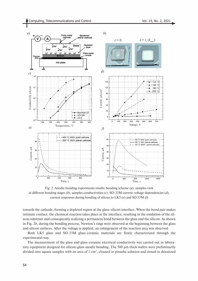
Computing, Telecommunications and Control Vol. 14, No. 2, 2021
54
Fig. 2. Anodic bonding experiments results: bonding scheme (a), samples view
at different bonding stages (b), samples conductivities (c), SO-33M current-voltage dependencies (d),
current responses during bonding of silicon to LK5 (e) and SO 33M (f)
towards the cathode, forming a depleted region at the glass-silicon interface. When the bond pair makes intimate contact, the chemical reaction takes place at the interface, resulting in the oxidation of the sil-icon substrate and consequently realizing a permanent bond between the glass and the silicon. As shown in Fig. 2b, during the bonding process, Newton’s rings were observed at the beginning between the glass and silicon surfaces. After the voltage is applied, an enlargement of the reaction area was observed.
Both LK5 glass and SO-33M glass-ceramic materials are firstly characterized through the experimental way.
The measurement of the glass and glass-ceramic electrical conductivity was carried out in labora-tory equipment designed for silicon-glass anodic bonding. The 500 μm thick wafers were preliminarily divided into square samples with an area of 1 cm2, cleaned in piranha solution and rinsed in deionized
t = 0 t = t1 (I
max)
Cur
ren
t, μ
A/c
m2
Cur
ren
t, μ
A
Cur
ren
t, μ
AC
ondu
ctiv
ity,
μS
/cm
Voltage, VTemperature,
Time, s Time, s
a) b)
d)
e) f)
c)
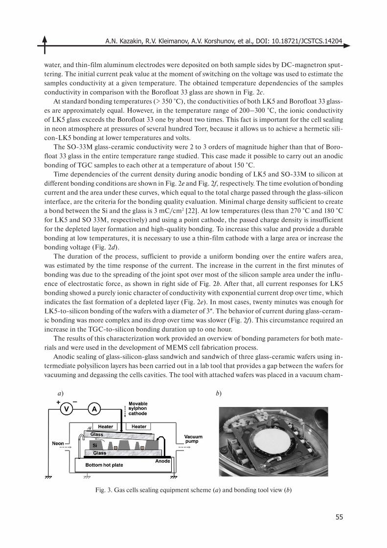
A.N. Kazakin, R.V. Kleimanov, A.V. Korshunov, et al., DOI: 10.18721/JCSTCS.14204
55
water, and thin-film aluminum electrodes were deposited on both sample sides by DC-magnetron sput-tering. The initial current peak value at the moment of switching on the voltage was used to estimate the samples conductivity at a given temperature. The obtained temperature dependencies of the samples conductivity in comparison with the Borofloat 33 glass are shown in Fig. 2c.
At standard bonding temperatures (> 350 °C), the conductivities of both LK5 and Borofloat 33 glass-es are approximately equal. However, in the temperature range of 200–300 °C, the ionic conductivity of LK5 glass exceeds the Borofloat 33 one by about two times. This fact is important for the cell sealing in neon atmosphere at pressures of several hundred Torr, because it allows us to achieve a hermetic sili-con-LK5 bonding at lower temperatures and volts.
The SO-33M glass-ceramic conductivity were 2 to 3 orders of magnitude higher than that of Boro-float 33 glass in the entire temperature range studied. This case made it possible to carry out an anodic bonding of TGC samples to each other at a temperature of about 150 °C.
Time dependencies of the current density during anodic bonding of LK5 and SO-33M to silicon at different bonding conditions are shown in Fig. 2e and Fig. 2f, respectively. The time evolution of bonding current and the area under these curves, which equal to the total charge passed through the glass-silicon interface, are the criteria for the bonding quality evaluation. Minimal charge density sufficient to create a bond between the Si and the glass is 3 mC/cm2 [22]. At low temperatures (less than 270 °C and 180 °C for LK5 and SO 33M, respectively) and using a point cathode, the passed charge density is insufficient for the depleted layer formation and high-quality bonding. To increase this value and provide a durable bonding at low temperatures, it is necessary to use a thin-film cathode with a large area or increase the bonding voltage (Fig. 2d).
The duration of the process, sufficient to provide a uniform bonding over the entire wafers area, was estimated by the time response of the current. The increase in the current in the first minutes of bonding was due to the spreading of the joint spot over most of the silicon sample area under the influ-ence of electrostatic force, as shown in right side of Fig. 2b. After that, all current responses for LK5 bonding showed a purely ionic character of conductivity with exponential current drop over time, which indicates the fast formation of a depleted layer (Fig. 2e). In most cases, twenty minutes was enough for LK5-to-silicon bonding of the wafers with a diameter of 3ʺ. The behavior of current during glass-ceram-ic bonding was more complex and its drop over time was slower (Fig. 2f). This circumstance required an increase in the TGC-to-silicon bonding duration up to one hour.
The results of this characterization work provided an overview of bonding parameters for both mate-rials and were used in the development of MEMS cell fabrication process.
Anodic sealing of glass-silicon-glass sandwich and sandwich of three glass-ceramic wafers using in-termediate polysilicon layers has been carried out in a lab tool that provides a gap between the wafers for vacuuming and degassing the cells cavities. The tool with attached wafers was placed in a vacuum cham-
Fig. 3. Gas cells sealing equipment scheme (a) and bonding tool view (b)
a) b)
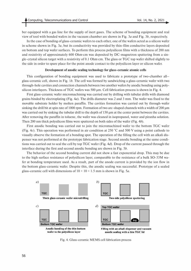
Computing, Telecommunications and Control Vol. 14, No. 2, 2021
56
Fig. 4. Glass-ceramic MEMS cell fabrication process
ber equipped with a gas line for the supply of inert gases. The scheme of bonding equipment and real view of tool with bonded wafers in the vacuum chamber are shown in Fig. 3a and Fig. 3b, respectively.
In the case of bonding of glass-ceramic wafers to each other, one of the wafers acted as a silicon wafer in scheme shown in Fig. 3a, but its conductivity was provided by thin-film conductive layers deposited on bottom and top wafer surfaces. To perform this process polysilicon films with a thickness of 200 nm and resistivity of approximately 600 Ohm·cm was deposited by DC-magnetron sputtering from a sin-gle-crystal silicon target with a resistivity of 0.1 Ohm·cm. The glass or TGC top wafer shifted slightly to the side in order to spare place for the point anode contact to the polysilicon layer or silicon wafer.
Development of anodic sealing technology for glass-ceramic atomic cells
This configuration of bonding equipment was used to fabricate a prototype of two-chamber all–glass-ceramic cell, shown in Fig. 1b. The cell was formed by sandwiching a glass-ceramic wafer with two through-hole cavities and connection channels between two another wafers by anodic bonding using poly-silicon interlayers. Thickness of TGC wafers was 500 μm. Cell fabrication process is shown in Fig. 4.
First glass-ceramic wafer micromachining was carried out by drilling with tubular drills with diamond grains binded by electroplating (Fig. 4a). The drills diameter was 2 and 3 mm. The wafer was fixed to the movable substrate holder by molten paraffin. The cavities formation was carried out by through-wafer sinking the drill bit at spin rate of 1000 rpm. Formation of two arc-shaped channels with a width of 200 μm was carried out by sinking the tubular drill to the depth of 150 μm at the center point between the cavities. After removing the paraffin in toluene, the wafer was cleaned in isopropanol, water and piranha solution. Then 200 nm thick polysilicon films were sputtered on both sides of the wafer (Fig. 4b).
First anodic bonding was carried out to join the micromachined wafer to the bottom TGC wafer (Fig. 4c). This operation was performed in air condition at 250 °C and 500 V using a point cathode to visually observe the formation of a bonding spot. The operation of the filling the cell with an alkali dis-penser was not performed at the prototype fabrication stage. Second anodic bonding at the same condi-tions was carried out to seal the cell by top TGC wafer (Fig. 4d). Drop of the current passed through the interface during the first and second anodic bonding are shown in Fig. 5b.
The behavior of the second bonding current did not show a fast exponential drop. This may be due to the high surface resistance of polysilicon layer, comparable to the resistance of a bulk SO-33M wa-fer at bonding temperature used. As a result, part of the anode current is provided by the ion flow in the bottom glass-ceramic wafer. Despite this, the anodic sealing was successful. Prototype of a sealed glass-ceramic cell with dimensions of 10 × 10 × 1.5 mm is shown in Fig. 5a.
a) b)
c) d)
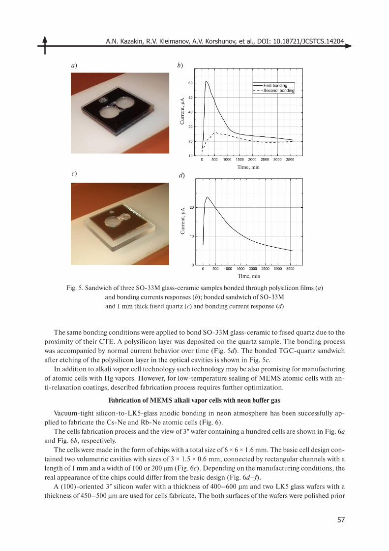
A.N. Kazakin, R.V. Kleimanov, A.V. Korshunov, et al., DOI: 10.18721/JCSTCS.14204
57
The same bonding conditions were applied to bond SO-33M glass-ceramic to fused quartz due to the proximity of their CTE. A polysilicon layer was deposited on the quartz sample. The bonding process was accompanied by normal current behavior over time (Fig. 5d). The bonded TGC-quartz sandwich after etching of the polysilicon layer in the optical cavities is shown in Fig. 5c.
In addition to alkali vapor cell technology such technology may be also promising for manufacturing of atomic cells with Hg vapors. However, for low-temperature sealing of MEMS atomic cells with an-ti-relaxation coatings, described fabrication process requires further optimization.
Fabrication of MEMS alkali vapor cells with neon buffer gas
Vacuum-tight silicon-to-LK5-glass anodic bonding in neon atmosphere has been successfully ap-plied to fabricate the Cs-Ne and Rb-Ne atomic cells (Fig. 6).
The cells fabrication process and the view of 3ʺ wafer containing a hundred cells are shown in Fig. 6a and Fig. 6b, respectively.
The cells were made in the form of chips with a total size of 6 × 6 × 1.6 mm. The basic cell design con-tained two volumetric cavities with sizes of 3 × 1.5 × 0.6 mm, connected by rectangular channels with a length of 1 mm and a width of 100 or 200 μm (Fig. 6c). Depending on the manufacturing conditions, the real appearance of the chips could differ from the basic design (Fig. 6d–f).
A (100)-oriented 3ʺ silicon wafer with a thickness of 400–600 μm and two LK5 glass wafers with a thickness of 450–500 μm are used for cells fabricate. The both surfaces of the wafers were polished prior
Fig. 5. Sandwich of three SO-33M glass-ceramic samples bonded through polysilicon films (a)
and bonding currents responses (b); bonded sandwich of SO-33M
and 1 mm thick fused quartz (c) and bonding current response (d)
a)
c) d)
b)
Time, min
Time, min
Cur
ren
t, μ
AC
urre
nt,
μA
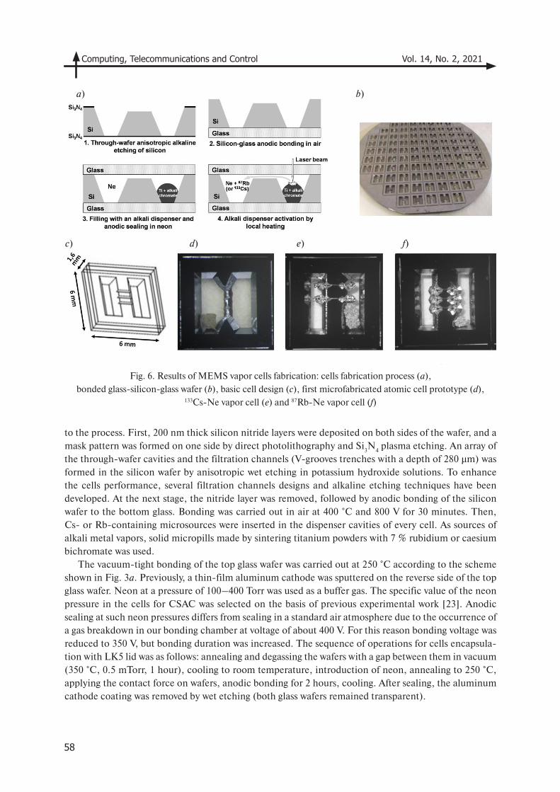
Computing, Telecommunications and Control Vol. 14, No. 2, 2021
58
Fig. 6. Results of MEMS vapor cells fabrication: cells fabrication process (a),
bonded glass-silicon-glass wafer (b), basic cell design (c), first microfabricated atomic cell prototype (d), 133Cs-Ne vapor cell (e) and 87Rb-Ne vapor cell (f)
to the process. First, 200 nm thick silicon nitride layers were deposited on both sides of the wafer, and a mask pattern was formed on one side by direct photolithography and Si
3N
4 plasma etching. An array of
the through-wafer cavities and the filtration channels (V-grooves trenches with a depth of 280 μm) was formed in the silicon wafer by anisotropic wet etching in potassium hydroxide solutions. To enhance the cells performance, several filtration channels designs and alkaline etching techniques have been developed. At the next stage, the nitride layer was removed, followed by anodic bonding of the silicon wafer to the bottom glass. Bonding was carried out in air at 400 °C and 800 V for 30 minutes. Then, Cs- or Rb-containing microsources were inserted in the dispenser cavities of every cell. As sources of alkali metal vapors, solid micropills made by sintering titanium powders with 7 % rubidium or caesium bichromate was used.
The vacuum-tight bonding of the top glass wafer was carried out at 250 °C according to the scheme shown in Fig. 3a. Previously, a thin-film aluminum cathode was sputtered on the reverse side of the top glass wafer. Neon at a pressure of 100–400 Torr was used as a buffer gas. The specific value of the neon pressure in the cells for CSAC was selected on the basis of previous experimental work [23]. Anodic sealing at such neon pressures differs from sealing in a standard air atmosphere due to the occurrence of a gas breakdown in our bonding chamber at voltage of about 400 V. For this reason bonding voltage was reduced to 350 V, but bonding duration was increased. The sequence of operations for cells encapsula-tion with LK5 lid was as follows: annealing and degassing the wafers with a gap between them in vacuum (350 °C, 0.5 mTorr, 1 hour), cooling to room temperature, introduction of neon, annealing to 250 °C, applying the contact force on wafers, anodic bonding for 2 hours, cooling. After sealing, the aluminum cathode coating was removed by wet etching (both glass wafers remained transparent).
a) b)
c) d) e) f)
A.N. Kazakin, R.V. Kleimanov, A.V. Korshunov, et al., DOI: 10.18721/JCSTCS.14204
59
REFERENCES
1. Kitching J. Chip-scale atomic devices. Applied Physics Reviews, 2018, No. 5, 031302. DOI: 10.10-
63/1.5026238
2. Lozov R.K., Baranov A.A., Ermak S.V., Semenov V.V. Comparison of orientational error of an optically
pumped quantum sensor in on-board equipment of Galileo and GPS satellite systems. Journal of Physics: Con-
ference Series, 2019, Vol. 1236, 012077. DOI: 10.1088/1742-6596/1236/1/012077
3. Borisevich E., Korolev A., Lozov R. The orbits shape influence of the navigation satellite systems on posi-
tioning accuracy. International Youth Conference on Electronics, Telecommunications and Information Technolo-
At the final stage of the cells fabrication process, the bonded glass-silicon-glass wafer was divided into separate chips, followed by the activation of the alkali dispensers by local laser heating according to a well-known technique [14].
Fig. 6d shows the photo of the first cell filled with 87Rb vapor and Ne gas under the pressure of 200 Torr fabricated by authors in 2014. The cell cavities thickness was 400 μm. The relative short-term frequency stability was estimated as 1.4·10–10 s–1/2 [15].
Fig. 6e and Fig. 6f show the photos of the 133Cs and 87Rb vapor cells with the Ne pressure of 300 Torr, respectively. These cells have improved design and 600 μm thick cavities. Preliminary experiments have shown that cell parameters dispersion for the width and intensity of the Hanle and CPT signals is from 30 to 50 %, which can be explained by differences in the modes of laser activation of cells. Relative short-term frequency stability for best samples is 2.5·10–11 s–1/2 [13].
Conclusion
We analyzed the dependence of the chip-scale atomic clock short-term and long-term frequency stability on the structural and technological parameters of the MEMS alkali vapor cells with buffer gases or anti-relaxation wall coatings. As the analysis showed, to improve these parameters, it is desirable to reduce the temperature of the anode bonding of silicon and glass used for MEMS cells sealing, since the exact composition of the cell inner atmosphere significantly depends on the results of this opera-tion. Two alternative materials, LK5 glass and SO-33M glass-ceramic, with increased ionic conductivity compared to the conventional glasses used in MEMS technology have been experimentally investigated to develop low-temperature anodic bonding with silicon, fused quartz, and to each other.
Transparent lithium aluminosilicate glass-ceramics SO-33M with a near-zero coefficient of thermal expansion provided acceptable quality of anodic sealing at a temperature of 150 °C. Intermediate thin-film polysilicon layers were used to bond the glass-ceramic wafers to each other and to fused quartz. The prototypes of MEMS cells with optical windows made of glass-ceramic and fused quartz were made. The developed technology can be promising for the fabrication of alkali vapor cells with organic anti-re-laxation coating.
We developed a technology of MEMS atomic cells containing rubidium or caesium vapors in an at-mosphere of neon buffer gas. Two-chamber silicon cells containing an optical cavity, shallow filtration channels and a technical container for a solid alkali microdispenser have been fabricated. We sealed the cells by means of silicon-to-LK5-glass anodic bonding at a temperature of 250 °C. The best micro-fabricated cells allowed us to obtain estimates of the CPT-resonance frequency stability at the level of 2.5·10–11 at 1 s. An acceptable reproducibility of the parameters of the cell from various series confirms the feasibility of introducing the developed MEMS technology in the implementation of small-sized quantum frequency standard.
This work was carried out in Peter the Great St.Petersburg Polytechnic University and was supported by a
grant of Russian Science Foundation (project No. 20-19-00146).
Computing, Telecommunications and Control Vol. 14, No. 2, 2021
60
gies. Springer Proceedings in Physics, Springer, Cham., 2021, Vol. 255, Pp. 761–775. DOI: 10.1007/978-3-030-
58868-7_83
4. Bobrov M.A., Blokhin S.A., Maleev N.A., Blokhin A.A., Vasyl’ev A.P., Kuzmenkov A.G., Pazgalev A.S.,
Petrenko M.V., Dmitriev S.P., Vershovskii A.K., Ustinov V.M., Novikov I.I., Karachinskii L.Ya. Optical-
ly pumped non-zero field magnetometric sensor for the magnetoencephalographic systems using intra-cav-
ity contacted VCSELs with rhomboidal oxide current aperture. Journal of Physics: Conference Series, 2020,
Vol. 1697, 012175. DOI: 10.1088/1742-6596/1697/1/012175
5. Knapkiewicz P. Alkali vapor MEMS cells technology toward high-vacuum self-pumping MEMS cell for
atomic spectroscopy. Micromachines, 2018, No. 9, 405. DOI: 10.3390/mi9080405
6. Rushton J.A., Aldous M., Himsworth M.D. Contributed review: The feasibility of a fully miniaturized
magneto-optical trap for portable ultracold quantum technology. Review of Scientific Instruments, 2014, Vol. 85,
121501. DOI: 10.1063/1.4904066
7. Knappe S., Schwindt P.D.D., Gerginov V., Shah V., Hollberg L., Kitching J., Liew L., Moreland J. Mi-
crofabricated atomic clocks at NIST. Proceedings of the 36th Annual Precise Time and Time Interval Systems and
Applications Meeting, Washington, D.C., Dec. 2004, Pp. 383–392.
8. Petremand Y., Affolderbach C., Straessle R., Pellaton M., Briand D., Mileti G., de Rooij N.F. Microfab-
ricated rubidium vapour cell with a thick glass core for small-scale atomic clock applications. Journal of Micro-
mechanics and Microengineering, 2012, Vol. 22, No. 2, 025013. DOI: 10.1088/0960-1317/22/2/025013
9. Gorecki C. Development of first European chip-scale atomic clocks: technologies, assembling and me-
trology. Procedia Engineering, 2012, No. 47, Pp. 898–903. DOI: 10.1016/j.proeng.2012.09.292
10. Vicarini R., Maurice V., Abdel Hafiz M., Rutkowski J., Gorecki C., Passilly N., Ribetto L., Gaff V.,
Volant V., Galliou S., Boudot R. Demonstration of the mass-producible feature of a Cs vapor microcell tech-
nology for miniature atomic clocks. Sensors and Actuators A, 2018, Vol. 280, Pp. 99–106. DOI: 10.1016/j.
sna.2018.07.032
11. Vanier J., Levine M., Kendig S., Janssen D., Everson C., Delaney M. Practical realization of a passive co-
herent population trapping frequency standard. IEEE Transactions on Instrumentation and Measurement, 2005,
Vol. 54, No. 6, Pp. 2531–2539. DOI: 10.1109/TIM.2005.858120
12. Knappe S. MEMS Atomic clocks. Comprehensive Microsystems, 2008, Vol. 3, Pp. 571–612.
13. Bobrov M.A., Blokhin S.A., Maleev N.A., Blokhin A.A., Vasyl’ev A.P., Kuzmenkov A.G., Gladyshev A.G.,
Novikov I.I., Petrenko M.V., Ospennikov A.M., Ermak S.V., Ustinov V.M. Effect of coherent population trap-
ping in a compact microfabricated Cs gas cell pumped by intra-cavity contacted VCSELs with rhomboidal
oxide current aperture. Journal of Physics: Conference Series, 2019, Vol. 1400, 077014. DOI: 10.1088/1742-
6596/1400/7/077014
14. Hasegawa M., Chutani R.K., Gorecki C., Boudot R., Dziuban P., Giordano V., Clatot S., Mauri L. Mi-
crofabrication of cesium vapor cells with buffer gas for MEMS atomic clocks. Sensors and Actuators A, 2011,
Vol. 167, Pp. 594–601. DOI: 10.1016/j.sna.2011.02.039
15. Ermak S.V., Semenov V.V., Piatyshev E.N., Kazakin A.N., Komarevtsev I.M., Velichko E.N., Davydov
V.V., Petrenko M.V. Microfabricated cells for chip-scale atomic clock based on coherent population trapping:
Fabrication and investigation. St. Petersburg Polytechnical University Journal: Physics and Mathematics, 2015,
No. 1, Pp. 37–41. DOI: 10.1016/j.spjpm.2015.03.003
16. Knappe S., Schwind P.D.D., Shah V., Hollberg L., Kitching J., Liew L., Moreland J. A chip-scale atomic
clock based on 87Rb with improwed frequency stability. Optics Express, 2005, Vol. 13, No. 4, Pp. 1249–1253.
17. Straessle R., Pellaton M., Affolderbach C., Pétremand Y., Briand D., Mileti G., de Rooij N.F. Microfab-
ricated alkali vapor cell with anti-relaxation wall coating. Applied Physics Letters, 2014, Vol. 105, 043502. DOI:
10.1063/1.4891248
18. Knapkiewicz P. Technological assessment of MEMS alkali vapor cells for atomic references. Microma-
chines, 2019, No. 10, 25. DOI: 10.3390/mi10010025
A.N. Kazakin, R.V. Kleimanov, A.V. Korshunov, et al., DOI: 10.18721/JCSTCS.14204
61
Received 08.06.2021.
СПИСОК ЛИТЕРАТУРЫ
1. Kitching J. Chip-scale atomic devices // Applied Physics Reviews. 2018. No. 5. 031302. DOI: 10.10-
63/1.5026238
19. Dziuban J.A. Bonding in microsystem technology. Springer Series in Advanced Microelectronics, 2006,
Vol. 24, 331 p.
20. Wallis G., Pomerantz D. Field assisted glass-metal sealing. Journal of Applied Physics, 1969, Vol. 40,
No. 10, Pp. 3946–3949.
21. Berthold A., Nicola L., Sarro P.M., Vellekoop M.J. Glass-to-glass anodic bonding with standard IC
technology thin films as intermediate layers. Sensors and Actuators, 2000, Vol. 82, Pp. 224–228.
22. van Elp J., Giesen P.T.M., van der Velde J.J. Anodic bonding using the low expansion glass ceramic
Zerodur. Journal of Vacuum Science & Technology B, 2005, Vol. 23, No. 1, Pp. 96–98. DOI: 10.1116/1.1839912
23. Fedorov M.I., Ermak S.V., Petrenko M.V., Pyatyshev E.N., Semenov V.V. Investigation of coherent pop-
ulation trapping signals in 87Rb cells with buffer gas. Journal of Physics: Conference Series, 2016, Vol. 769,
012046. DOI: 10.1088/1742-6596/769/1/012046
24. Gerginov V., Knappe S., Shah V., Schwind P.D.D., Hollberg L., Kitching J. Long-term frequency insta-
bility of atomic frequency references based on coherent population trapping and microfabricated vapor cells.
Journal of Optical Society of America B, 2006, Vol. 23, No. 4, Pp. 593–597.
25. Kobtsev S., Radnatarov D., Khripunov S., Popkov I., Andryushkov V., Steshchenko T. Stability properties
of an Rb CPT atomic clock with buffer-gas-free cells under dynamic excitation. Journal of the Optical Society of
America B, 2019, Vol. 36, No. 10, Pp. 2700–2704, DOI: 10.1364/JOSAB.36.002700
26. Chi H., Quan W., Zhang J., Zhao L., Fang J. Advances in anti-relaxation coatings of alkali-metal vapor
cells. Applied Surface Science, 2020, Vol. 501, 143897. DOI: 10.1016/j.apsusc.2019.143897
27. Ji Y., Shang J., Gan Q., Wu L. Wafer-level micro alkali vapor cells with anti-relaxation coating compat-
ible with MEMS packaging for chip-scale atomic magnetometers. 2017 IEEE 67th Electronic Components and
Technology Conference (ECTC), 2017, Pp. 2116–2120. DOI: 10.1109/ECTC.2017.136
28. Norton F.J. Permeation of Gases through Solids. Journal of Applied Physics, 1957, No. 28, Pp. 34–39.
DOI: 10.1063/1.1722570
29. Abdullah S., Affolderbach C., Gruet F., Mileti G. Aging studies on micro-fabricated alkali buffer-gas cells
for miniature atomic clocks. Applied Physics Letters, 2015, Vol. 106, 163505.
30. Dellis A.T., Shah V., Donley E.A., Knappe S., Kitching J. Low helium permeation cells for atomic mi-
crosystems technology. Optics Letters, 2016, Vol. 41, No. 12, Pp. 2775–2778. DOI: 10.1364/OL.41.002775
31. Sinev L.S., Ryabov V.T. Reducing thermal mismatch stress in anodically bonded silicon-glass wafers:
theoretical estimation. Journal of Micro/Nanolithography, MEMS, and MOEMS, 2017, Vol. 16, No. 1, 015003.
DOI: 10.1117/1.JMM.16.1.015003
32. Dymshits O., Shepilov M., Zhilin A. Transparent glass-ceramics for optical applications, 2017, MRS
Bulletin, Vol. 42, Pp. 200–205. DOI: 10.1557/mrs.2017.29
33. Hu X., Mackowiak P., Baeuscher M., Zhang Y., Wang B., Hansen U. Low stress solution of anodic
bonding technology with SW-YY glass for sensitive MEMS. 2018 IEEE 20th Electronics Packaging Technology
Conference, 2018, Pp. 251–255. DOI: 10.1109/EPTC.2018.8654362
34. Shoji S., Kikuchi H., Torigoe H. Anodic bonding below 180 °C for packaging and assembling of MEMS
using lithium aluminosilicate-β-quartz glass-ceramic. Proceedings IEEE the 10th Annual International Workshop
on Micro Electro Mechanical Systems. An Investigation of Micro Structures, Sensors, Actuators, Machines and Ro-
bots, 1997, Pp. 482–487. DOI: 10.1109/MEMSYS.1997.581907
Computing, Telecommunications and Control Vol. 14, No. 2, 2021
62
2. Lozov R.K., Baranov A.A., Ermak S.V., Semenov V.V. Comparison of orientational error of an optically
pumped quantum sensor in on-board equipment of Galileo and GPS satellite systems // J. of Physics: Conf.
Ser. 2019. Vol. 1236. 012077. DOI: 10.1088/1742-6596/1236/1/012077
3. Borisevich E., Korolev A., Lozov R. The orbits shape influence of the navigation satellite systems on posi-
tioning accuracy // Internat. Youth Conf. on Electronics, Telecommunications and Information Technologies.
Springer Proceedings in Physics. Springer, Cham., 2021. Vol. 255. Pp. 761–775. DOI: 10.1007/978-3-030-
58868-7_83
4. Bobrov M.A., Blokhin S.A., Maleev N.A., Blokhin A.A., Vasyl’ev A.P., Kuzmenkov A.G., Pazgalev A.S.,
Petrenko M.V., Dmitriev S.P., Vershovskii A. K., Ustinov V.M., Novikov I.I., Karachinskii L.Ya. Optically
pumped non-zero field magnetometric sensor for the magnetoencephalographic systems using intra-cavity
contacted VCSELs with rhomboidal oxide current aperture // J. of Physics: Conf. Ser. 2020. Vol. 1697. 012175.
DOI: 10.1088/1742-6596/1697/1/012175
5. Knapkiewicz P. Alkali vapor MEMS cells technology toward high-vacuum self-pumping MEMS cell for
atomic spectroscopy // Micromachines. 2018. No. 9. 405. DOI: 10.3390/mi9080405
6. Rushton J.A., Aldous M., Himsworth M.D. Contributed review: The feasibility of a fully miniaturized
magneto-optical trap for portable ultracold quantum technology // Review of Scientific Instruments. 2014.
Vol. 85. 121501. DOI: 10.1063/1.4904066
7. Knappe S., Schwindt P.D.D., Gerginov V., Shah V., Hollberg L., Kitching J., Liew L., Moreland J. Mi-
crofabricated atomic clocks at NIST // Proc. of the 36th Annual Precise Time and Time Interval Systems and
Applications Meeting. Washington, D.C., Dec. 2004. Pp. 383–392.
8. Petremand Y., Affolderbach C., Straessle R., Pellaton M., Briand D., Mileti G., de Rooij N.F. Microfab-
ricated rubidium vapour cell with a thick glass core for small-scale atomic clock applications // J. of Microme-
chanics and Microengineering. 2012. Vol. 22. No. 2. 025013. DOI: 10.1088/0960-1317/22/2/025013
9. Gorecki C. Development of first European chip-scale atomic clocks: technologies, assembling and me-
trology // Procedia Engineering. 2012. No. 47. Pp. 898–903. DOI: 10.1016/j.proeng.2012.09.292
10. Vicarini R., Maurice V., Abdel Hafiz M., Rutkowski J., Gorecki C., Passilly N., Ribetto L., Gaff V.,
Volant V., Galliou S., Boudot R. Demonstration of the mass-producible feature of a Cs vapor microcell tech-
nology for miniature atomic clocks // Sensors and Actuators A. 2018. Vol. 280. Pp. 99–106. DOI: 10.1016/j.
sna.2018.07.032
11. Vanier J., Levine M., Kendig S., Janssen D., Everson C., Delaney M. Practical realization of a passive
coherent population trapping frequency standard // IEEE Transactions on Instrumentation and Measurement.
2005. Vol. 54. No. 6. Pp. 2531–2539. DOI: 10.1109/TIM.2005.858120
12. Knappe S. MEMS atomic clocks // Comprehensive Microsystems. 2008. Vol. 3. Pp. 571–612.
13. Bobrov M.A., Blokhin S.A., Maleev N.A., Blokhin A.A., Vasyl’ev A.P., Kuzmenkov A.G., Gladyshev
A.G., Novikov I.I., Petrenko M.V., Ospennikov A.M., Ermak S.V., Ustinov V.M. Effect of coherent pop-
ulation trapping in a compact microfabricated Cs gas cell pumped by intra-cavity contacted VCSELs with
rhomboidal oxide current aperture // J. of Physics: Conf. Ser. 2019. Vol. 1400. 077014. DOI: 10.1088/1742-
6596/1400/7/077014
14. Hasegawa M., Chutani R.K., Gorecki C., Boudot R., Dziuban P., Giordano V., Clatot S., Mauri L. Mi-
crofabrication of cesium vapor cells with buffer gas for MEMS atomic clocks // Sensors and Actuators A. 2011.
Vol. 167. Pp. 594–601. DOI: 10.1016/j.sna.2011.02.039
15. Ermak S.V., Semenov V.V., Piatyshev E.N., Kazakin A.N., Komarevtsev I.M., Velichko E.N., Davy-
dov V.V., Petrenko M.V. Microfabricated cells for chip-scale atomic clock based on coherent population trap-
ping: Fabrication and investigation // St. Petersburg Polytechnical University Journal. Physics and Mathemat-
ics. 2015. No. 1. Pp. 37–41. DOI: 10.1016/j.spjpm.2015.03.003
16. Knappe S., Schwind P.D.D., Shah V., Hollberg L., Kitching J., Liew L., Moreland J. A chip-scale
atomic clock based on 87Rb with improwed frequency stability // Optics Express. 2005. Vol. 13. No. 4.
Pp. 1249–1253.
A.N. Kazakin, R.V. Kleimanov, A.V. Korshunov, et al., DOI: 10.18721/JCSTCS.14204
63
Статья поступила в редакцию 08.06.2021.
17. Straessle R., Pellaton M., Affolderbach C., Pétremand Y., Briand D., Mileti G., de Rooij N.F. Micro-
fabricated alkali vapor cell with anti-relaxation wall coating // Applied Physics Letters. 2014. Vol. 105. 043502.
DOI: 10.1063/1.4891248
18. Knapkiewicz P. Technological assessment of MEMS alkali vapor cells for atomic references // Microma-
chines. 2019. No. 10. 25. DOI: 10.3390/mi10010025
19. Dziuban J.A. Bonding in microsystem technology // Springer Series in Advanced Microelectronics.
2006. Vol. 24. 331 p.
20. Wallis G., Pomerantz D. Field assisted glass-metal sealing // J. of Applied Physics. 1969. Vol. 40. No. 10.
Pp. 3946–3949.
21. Berthold A., Nicola L., Sarro P.M., Vellekoop M.J. Glass-to-glass anodic bonding with standard IC
technology thin films as intermediate layers // Sensors and Actuators. 2000. Vol. 82. Pp. 224–228.
22. van Elp J., Giesen P.T.M., van der Velde J.J. Anodic bonding using the low expansion glass ceramic
Zerodur // J. of Vacuum Science & Technology B. 2005. Vol. 23. No. 1. Pp. 96–98. DOI: 10.1116/1.1839912
23. Fedorov M.I., Ermak S.V., Petrenko M.V., Pyatyshev E.N., Semenov V.V. Investigation of coherent pop-
ulation trapping signals in 87Rb cells with buffer gas // J. of Physics: Conf. Ser. 2016. Vol. 769. 012046. DOI:
10.1088/1742-6596/769/1/012046
24. Gerginov V., Knappe S., Shah V., Schwind P.D.D., Hollberg L., Kitching J. Long-term frequency insta-
bility of atomic frequency references based on coherent population trapping and microfabricated vapor cells //
J. of Optical Society of America B. 2006. Vol. 23. No. 4. Pp. 593–597.
25. Kobtsev S., Radnatarov D., Khripunov S., Popkov I., Andryushkov V., Steshchenko T. Stability properties
of an Rb CPT atomic clock with buffer-gas-free cells under dynamic excitation // J. of the Optical Society of
America B. 2019. Vol. 36. No. 10. Pp. 2700–2704. DOI: 10.1364/JOSAB.36.002700
26. Chi H., Quan W., Zhang J., Zhao L., Fang J. Advances in anti-relaxation coatings of alkali-metal vapor
cells // Applied Surface Science. 2020. Vol. 501. 143897. DOI: 10.1016/j.apsusc.2019.143897
27. Ji Y., Shang J., Gan Q., Wu L. Wafer-level micro alkali vapor cells with anti-relaxation coating compati-
ble with MEMS packaging for chip-scale atomic magnetometers // 2017 IEEE 67th Electronic Components and
Technology Conf. 2017. Pp. 2116–2120. DOI: 10.1109/ECTC.2017.136
28. Norton F.J. Permeation of gases through solids // J. of Applied Physics. 1957. No. 28. Pp. 34–39. DOI:
10.1063/1.1722570
29. Abdullah S., Affolderbach C., Gruet F., Mileti G. Aging studies on micro-fabricated alkali buffer-gas cells
for miniature atomic clocks // Applied Physics Letters. 2015. Vol. 106. 163505.
30. Dellis A.T., Shah V., Donley E.A., Knappe S., Kitching J. Low helium permeation cells for atomic mi-
crosystems technology // Optics Letters. 2016. Vol. 41. No. 12. Pp. 2775–2778. DOI: 10.1364/OL.41.002775
31. Sinev L.S., Ryabov V.T. Reducing thermal mismatch stress in anodically bonded silicon-glass wafers:
theoretical estimation // J. of Micro/Nanolithography, MEMS, and MOEMS. 2017. Vol. 16. No. 1. 015003.
DOI: 10.1117/1.JMM.16.1.015003
32. Dymshits O., Shepilov M., Zhilin A. Transparent glass-ceramics for optical applications // MRS Bulle-
tin. 2017. Vol. 42. Pp. 200–205. DOI: 10.1557/mrs.2017.29
33. Hu X., Mackowiak P., Baeuscher M., Zhang Y., Wang B., Hansen U. Low stress solution of anodic bond-
ing technology with SW-YY glass for sensitive MEMS // Proc. of the 20th Electronics Packaging Technology
Conf. 2018. Pp. 251–255. DOI: 10.1109/EPTC.2018.8654362
34. Shoji S., Kikuchi H., Torigoe H. Anodic bonding below 180 °C for packaging and assembling of MEMS
using lithium aluminosilicate-β-quartz glass-ceramic // Proc. IEEE the 10th Annual International Workshop on
Micro Electro Mechanical Systems. An Investigation of Micro Structures, Sensors, Actuators, Machines and
Robots. 1997. Pp. 482–487. DOI: 10.1109/MEMSYS.1997.581907
Computing, Telecommunications and Control Vol. 14, No. 2, 2021
64
THE AUTHORS / СВЕДЕНИЯ ОБ АВТОРАХ
Kazakin Alexei N.Казакин Алексей НиколаевичE-mail: [email protected]
Kleimanov Roman V.Клейманов Роман ВалерьевичE-mail: [email protected]
Korshunov Andrei V.Коршунов Андрей ВасильевичE-mail: [email protected]
Akulshin Yuri D.Акульшин Юрий ДмитриевичE-mail: [email protected]
Shashkin Aleksandr V.Шашкин Александр ВикторовичE-mail: [email protected]
© Санкт-Петербургский политехнический университет Петра Великого, 2021
V.V. Loboda, U.V. Salamatova, DOI: 10.18721/JCSTCS.14205
65
DOI: 10.18721/JCSTCS.14205УДК 621.3.049.7
CAPACITIVE MEMS MICROPHONES FOR MEDICAL APPLICATIONS
V.V. Loboda, U.V. SalamatovaPeter the Great St. Petersburg Polytechnic University,
St. Petersburg, Russian Federation
Microphones manufactured based on MEMS technology have been significantly applied in medicine. However, medical application requires more sensitive and low-frequency MEMS microphones. To achieve this goal capacitive microphones are the most appropriate as they have a low level of noise and high sensitivity compared to piezoelectric and piezoresistive microphones. The structure and materials enable to change electric parameters of microphones for better. To increase sensitivity it is possible to find a membrane structure when internal mechanical resistivity is minimal. When MEMS structures are ideally found, a frequencies range can be expanded. Membrane flexibility can be expanded by means of applying meshes at the edges, corrugations and springs.
Keywords: MEMS, capacitive microphone, low frequency microphone, sensitivity, membrans.
Citation: Loboda V.V., Salamatova U.V. Capacitive MEMS microphones for medical applications. Computing, Telecommunications and Control, 2021, Vol. 14, No. 2, Pp. 65–78. DOI: 10.18721/JCST-CS.14205
This is an open access article under the CC BY-NC 4.0 license (https://creativecommons.org/licenses/by-nc/4.0/).
ЁМКОСТНЫЕ МЭМС-МИКРОФОНЫ ДЛЯ МЕДИЦИНСКОГО ПРИМЕНЕНИЯ
В.В. Лобода, У.В. СаламатоваСанкт-Петербургский политехнический университет Петра Великого,
Санкт-Петербург, Российская Федерация
Микрофоны, произведенные по технологии МЭМС, находят новое применение и в медицине. Однако для медицины нужны более чувствительные и низкочастотные МЭМС-микрофоны. Для этой цели больше всего подходят ёмкостные микрофоны, так как они имеют низкий уровень шумов и высокую чувствительность по сравнению с пье-зоэлектрическими и пъезорезистивными микрофонами. Конструкция и материалы по-зволяют изменять электрические параметры микрофона в лучшую сторону. Повысить чувствительность можно путем подбора такого состава в структуре мембраны, при кото-ром будут минимальны внутренние механические напряжения. Подобрав конструкцию МЭМС, можно расширить и частотный диапазон. Увеличить податливость мембраны можно за счет применения прорезей по краям, гофр и пружин.
Ключевые слова: МЭМС, ёмкостный микрофон, низкочастотный микрофон, чувствитель-ность, мембраны.
Ссылка при цитировании: Loboda V.V., Salamatova U.V. Capacitive MEMS microphones for medical applications // Computing, Telecommunications and Control. 2021. Vol. 14. No. 2. Pp. 65–78. DOI: 10.18721/JCSTCS.14205
Cтатья открытого доступа, распространяемая по лицензии CC BY-NC 4.0 (https://creative-commons.org/licenses/by-nc/4.0/).
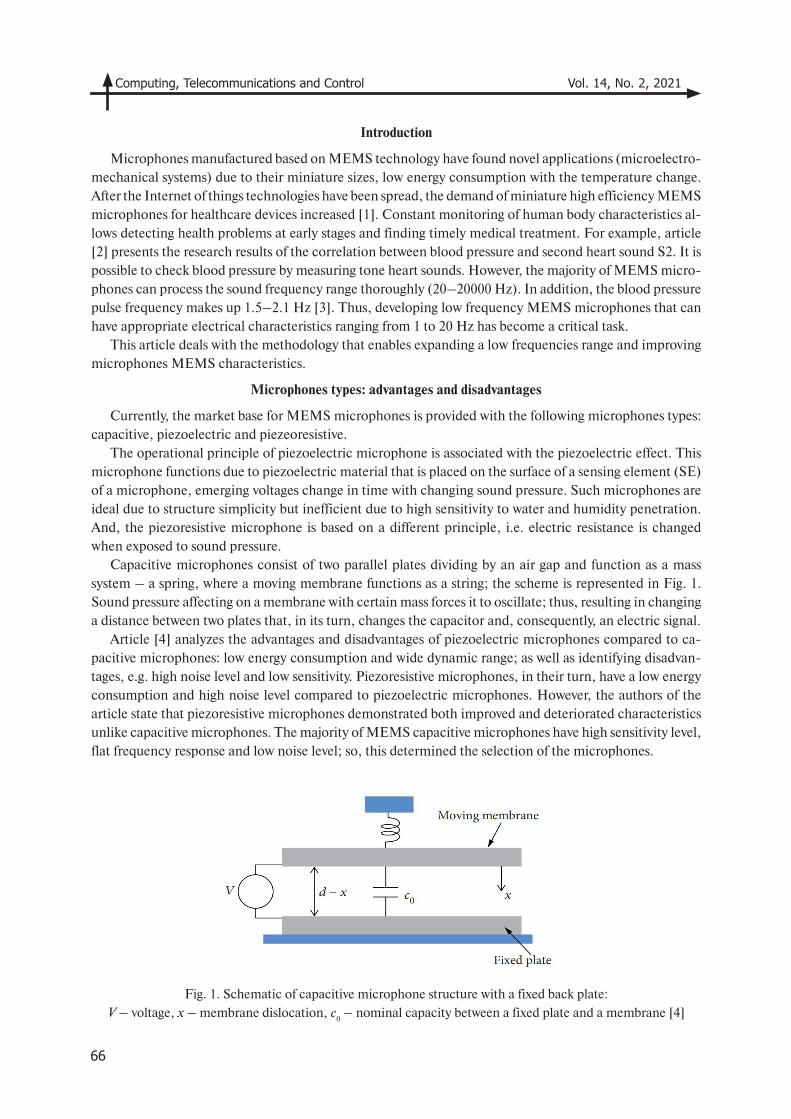
Computing, Telecommunications and Control Vol. 14, No. 2, 2021
66
Introduction
Microphones manufactured based on MEMS technology have found novel applications (microelectro-mechanical systems) due to their miniature sizes, low energy consumption with the temperature change. After the Internet of things technologies have been spread, the demand of miniature high efficiency MEMS microphones for healthcare devices increased [1]. Constant monitoring of human body characteristics al-lows detecting health problems at early stages and finding timely medical treatment. For example, article [2] presents the research results of the correlation between blood pressure and second heart sound S2. It is possible to check blood pressure by measuring tone heart sounds. However, the majority of MEMS micro-phones can process the sound frequency range thoroughly (20–20000 Hz). In addition, the blood pressure pulse frequency makes up 1.5–2.1 Hz [3]. Thus, developing low frequency MEMS microphones that can have appropriate electrical characteristics ranging from 1 to 20 Hz has become a critical task.
This article deals with the methodology that enables expanding a low frequencies range and improving microphones MEMS characteristics.
Microphones types: advantages and disadvantages
Currently, the market base for MEMS microphones is provided with the following microphones types: capacitive, piezoelectric and piezeoresistive.
The operational principle of piezoelectric microphone is associated with the piezoelectric effect. This microphone functions due to piezoelectric material that is placed on the surface of a sensing element (SE) of a microphone, emerging voltages change in time with changing sound pressure. Such microphones are ideal due to structure simplicity but inefficient due to high sensitivity to water and humidity penetration. And, the piezoresistive microphone is based on a different principle, i.e. electric resistance is changed when exposed to sound pressure.
Capacitive microphones consist of two parallel plates dividing by an air gap and function as a mass system – a spring, where a moving membrane functions as a string; the scheme is represented in Fig. 1. Sound pressure affecting on a membrane with certain mass forces it to oscillate; thus, resulting in changing a distance between two plates that, in its turn, changes the capacitor and, consequently, an electric signal.
Article [4] analyzes the advantages and disadvantages of piezoelectric microphones compared to ca-pacitive microphones: low energy consumption and wide dynamic range; as well as identifying disadvan-tages, e.g. high noise level and low sensitivity. Piezoresistive microphones, in their turn, have a low energy consumption and high noise level compared to piezoelectric microphones. However, the authors of the article state that piezoresistive microphones demonstrated both improved and deteriorated characteristics unlike capacitive microphones. The majority of MEMS capacitive microphones have high sensitivity level, flat frequency response and low noise level; so, this determined the selection of the microphones.
Fig. 1. Schematic of capacitive microphone structure with a fixed back plate:
V – voltage, х – membrane dislocation, с0 – nominal capacity between a fixed plate and a membrane [4]
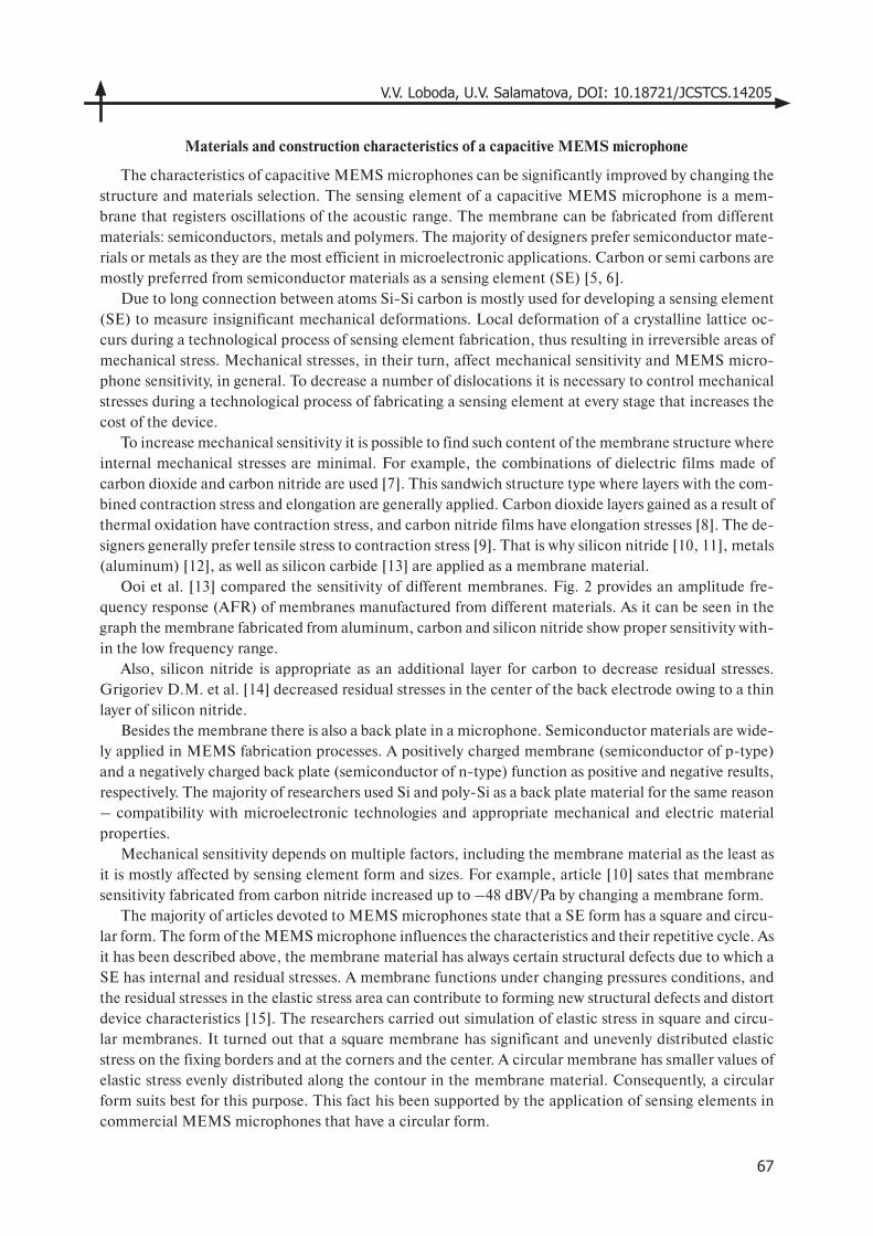
V.V. Loboda, U.V. Salamatova, DOI: 10.18721/JCSTCS.14205
67
Materials and construction characteristics of a capacitive MEMS microphone
The characteristics of capacitive MEMS microphones can be significantly improved by changing the structure and materials selection. The sensing element of a capacitive MEMS microphone is a mem-brane that registers oscillations of the acoustic range. The membrane can be fabricated from different materials: semiconductors, metals and polymers. The majority of designers prefer semiconductor mate-rials or metals as they are the most efficient in microelectronic applications. Carbon or semi carbons are mostly preferred from semiconductor materials as a sensing element (SE) [5, 6].
Due to long connection between atoms Si-Si carbon is mostly used for developing a sensing element (SE) to measure insignificant mechanical deformations. Local deformation of a crystalline lattice oc-curs during a technological process of sensing element fabrication, thus resulting in irreversible areas of mechanical stress. Mechanical stresses, in their turn, affect mechanical sensitivity and MEMS micro-phone sensitivity, in general. To decrease a number of dislocations it is necessary to control mechanical stresses during a technological process of fabricating a sensing element at every stage that increases the cost of the device.
To increase mechanical sensitivity it is possible to find such content of the membrane structure where internal mechanical stresses are minimal. For example, the combinations of dielectric films made of carbon dioxide and carbon nitride are used [7]. This sandwich structure type where layers with the com-bined contraction stress and elongation are generally applied. Carbon dioxide layers gained as a result of thermal oxidation have contraction stress, and carbon nitride films have elongation stresses [8]. The de-signers generally prefer tensile stress to contraction stress [9]. That is why silicon nitride [10, 11], metals (aluminum) [12], as well as silicon carbide [13] are applied as a membrane material.
Ooi et al. [13] compared the sensitivity of different membranes. Fig. 2 provides an amplitude fre-quency response (AFR) of membranes manufactured from different materials. As it can be seen in the graph the membrane fabricated from aluminum, carbon and silicon nitride show proper sensitivity with-in the low frequency range.
Also, silicon nitride is appropriate as an additional layer for carbon to decrease residual stresses. Grigoriev D.M. et al. [14] decreased residual stresses in the center of the back electrode owing to a thin layer of silicon nitride.
Besides the membrane there is also a back plate in a microphone. Semiconductor materials are wide-ly applied in MEMS fabrication processes. A positively charged membrane (semiconductor of p-type) and a negatively charged back plate (semiconductor of n-type) function as positive and negative results, respectively. The majority of researchers used Si and poly-Si as a back plate material for the same reason – compatibility with microelectronic technologies and appropriate mechanical and electric material properties.
Mechanical sensitivity depends on multiple factors, including the membrane material as the least as it is mostly affected by sensing element form and sizes. For example, article [10] sates that membrane sensitivity fabricated from carbon nitride increased up to –48 dBV/Pa by changing a membrane form.
The majority of articles devoted to MEMS microphones state that a SE form has a square and circu-lar form. The form of the MEMS microphone influences the characteristics and their repetitive cycle. As it has been described above, the membrane material has always certain structural defects due to which a SE has internal and residual stresses. A membrane functions under changing pressures conditions, and the residual stresses in the elastic stress area can contribute to forming new structural defects and distort device characteristics [15]. The researchers carried out simulation of elastic stress in square and circu-lar membranes. It turned out that a square membrane has significant and unevenly distributed elastic stress on the fixing borders and at the corners and the center. A circular membrane has smaller values of elastic stress evenly distributed along the contour in the membrane material. Consequently, a circular form suits best for this purpose. This fact his been supported by the application of sensing elements in commercial MEMS microphones that have a circular form.
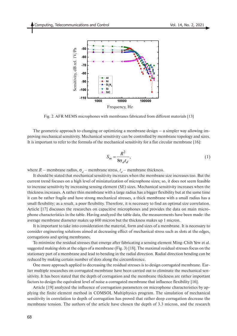
Computing, Telecommunications and Control Vol. 14, No. 2, 2021
68
Fig. 2. AFR MEMS microphones with membranes fabricated from different materials [13]
The geometric approach to changing or optimizing a membrane design – a simpler way allowing im-proving mechanical sensitivity. Mechanical sensitivity can be controlled by membrane topology and sizes. It is important to refer to the formula of the mechanical sensitivity for a flat circular membrane [16]:
where R – membrane radius, σd – membrane stress, td – membrane thickness. It should be stated that mechanical sensitivity increases when the membrane size increases too. But the
current trend focuses on a high level of miniaturization of microphone sizes; so, it does not seem feasible to increase sensitivity by increasing sensing element (SE) sizes. Mechanical sensitivity increases when the thickness increases. A rather thin membrane with a large radius has a bigger flexibility but at the same time it can be rather fragile and have strong mechanical stresses, а thick membrane with a small radius has a small flexibility; as a result, a poor flexibility. Therefore, it is necessary to find an optimal size correlation. Article [17] discusses the researches on capacitive microphones and provides the data on main micro-phone characteristics in the table. Having analyzed the table data, the measurements have been made: the average membrane diameter makes up 600 micron but the thickness makes up 1 micron.
It is important to take into consideration the material, form and sizes of a membrane. It is necessary to consider engineering solutions aimed at decreasing effect of mechanical stress such as slots at the edges, corrugations and spring membranes.
To minimize the residual stresses that emerge after fabricating a sensing element Ming-Chih Yew et al. suggested making slots at the edges of a membrane (Fig. 3) [18]. The maximal residual stresses focus on the stationary part of a membrane and lead to bending in the radial direction. Radial direction bending can be reduced by making certain number of slots along the circumference.
One more approach applied to decreasing the residual stresses is to design corrugated membrane. Ear-lier multiple researches on corrugated membrane have been carried out to eliminate the mechanical sen-sitivity. It has been stated that the depth of corrugation and the membrane thickness are rather important factors to design the equivalent level of noise a corrugated membrane that influence flexibility [16].
Article [19] analyzed the influence of corrugation parameters on microphone characteristics by ap-plying the finite element method in COMSOL Multiphysics program. The simulation of mechanical sensitivity in correlation to depth of corrugation has proved that rather deep corrugation decrease the membrane tension. The authors of the article have chosen the depth of 3.3 micron, and the research
2,
8md d
RSt
=σ
(1)
Frequency, Hz
Sen
siti
vity
, dB
rel
. 1V
/Pa
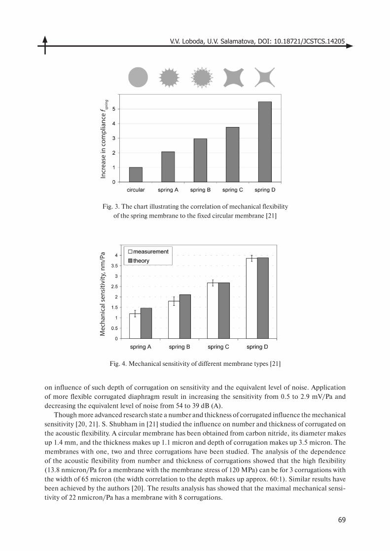
V.V. Loboda, U.V. Salamatova, DOI: 10.18721/JCSTCS.14205
69
on influence of such depth of corrugation on sensitivity and the equivalent level of noise. Application of more flexible corrugated diaphragm result in increasing the sensitivity from 0.5 to 2.9 mV/Pa and decreasing the equivalent level of noise from 54 to 39 dB (A).
Though more advanced research state a number and thickness of corrugated influence the mechanical sensitivity [20, 21]. S. Shubham in [21] studied the influence on number and thickness of corrugated on the acoustic flexibility. A circular membrane has been obtained from carbon nitride, its diameter makes up 1.4 mm, and the thickness makes up 1.1 micron and depth of corrugation makes up 3.5 micron. The membranes with one, two and three corrugations have been studied. The analysis of the dependence of the acoustic flexibility from number and thickness of corrugations showed that the high flexibility (13.8 nmicron/Pa for a membrane with the membrane stress of 120 MPa) can be for 3 corrugations with the width of 65 micron (the width correlation to the depth makes up approx. 60:1). Similar results have been achieved by the authors [20]. The results analysis has showed that the maximal mechanical sensi-tivity of 22 nmicron/Pa has a membrane with 8 corrugations.
Fig. 3. The chart illustrating the correlation of mechanical flexibility
of the spring membrane to the fixed circular membrane [21]
Fig. 4. Mechanical sensitivity of different membrane types [21]
Incr
ease
in c
ompl
ianc
e f sp
ring
Mec
hani
cal s
ensi
tivity
, nm
/Pa
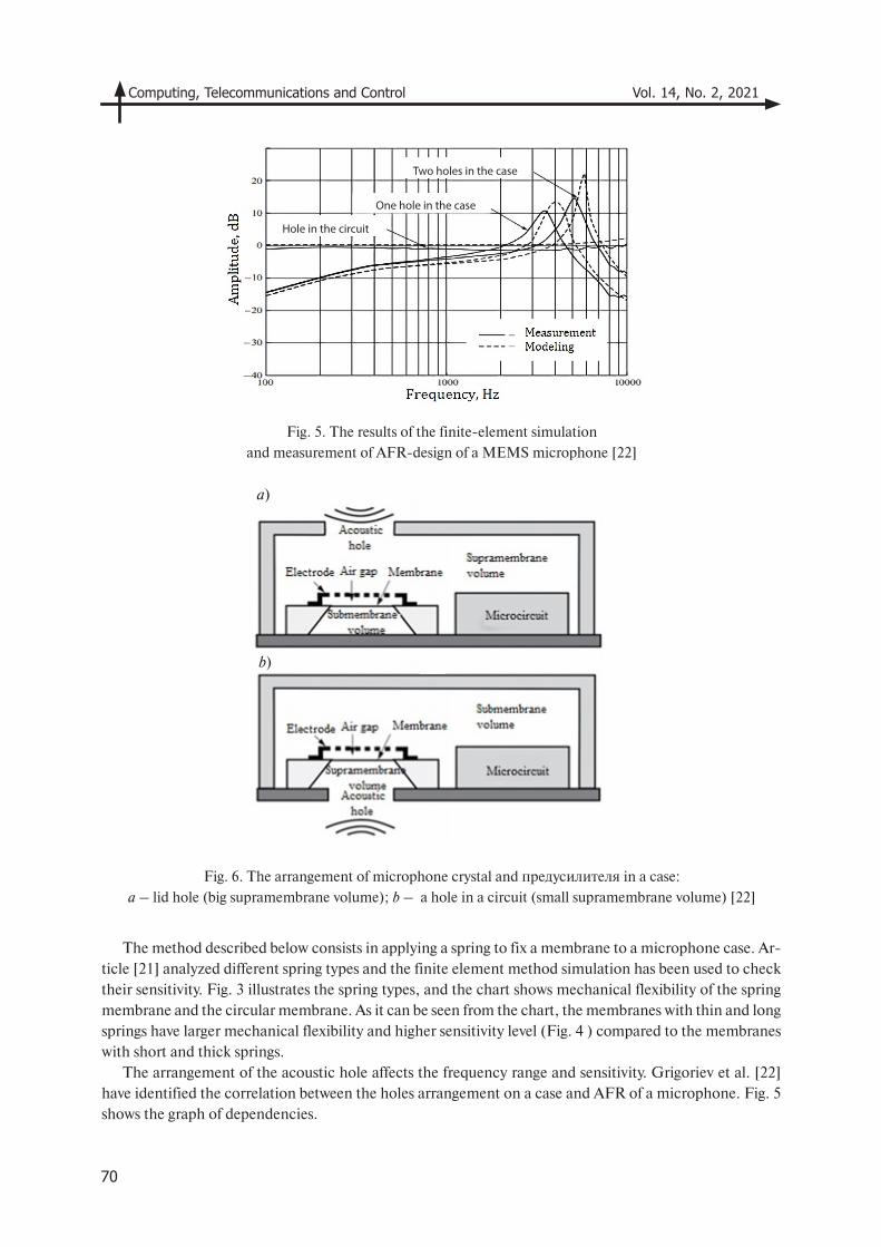
Computing, Telecommunications and Control Vol. 14, No. 2, 2021
70
Fig. 5. The results of the finite-element simulation
and measurement of AFR-design of a MEMS microphone [22]
Fig. 6. The arrangement of microphone crystal and предусилителя in a case:
a – lid hole (big supramembrane volume); b – a hole in a circuit (small supramembrane volume) [22]
The method described below consists in applying a spring to fix a membrane to a microphone case. Ar-ticle [21] analyzed different spring types and the finite element method simulation has been used to check their sensitivity. Fig. 3 illustrates the spring types, and the chart shows mechanical flexibility of the spring membrane and the circular membrane. As it can be seen from the chart, the membranes with thin and long springs have larger mechanical flexibility and higher sensitivity level (Fig. 4 ) compared to the membranes with short and thick springs.
The arrangement of the acoustic hole affects the frequency range and sensitivity. Grigoriev et al. [22] have identified the correlation between the holes arrangement on a case and AFR of a microphone. Fig. 5 shows the graph of dependencies.
a)
b)
Two holes in the case
One hole in the case
Hole in the circuit
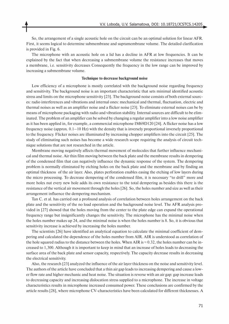
V.V. Loboda, U.V. Salamatova, DOI: 10.18721/JCSTCS.14205
71
So, the arrangement of a single acoustic hole on the circuit can be an optimal solution for linear AFR. First, it seems logical to determine submembrane and supramembrane volume. The detailed clarification is provided in Fig. 6.
The microphone with an acoustic hole on a lid has a decline in AFR at low frequencies. It can be explained by the fact that when decreasing a submembrane volume the resistance increases that moves a membrane, i.e. sensitivity decreases Consequently the frequency in the low range can be improved by increasing a submembrane volume.
Technique to decrease background noise
Low efficiency of a microphone is mostly correlated with the background noise regarding frequency and sensitivity. The background noise is an important characteristic that sets minimal identified acoustic stress and limits on the microphone sensitivity [23]. The background noise consists of both external sourc-es: radio interferences and vibrations and internal ones: mechanical and thermal, fluctuation, electric and thermal noises as well as an amplifier noise and a flicker noise [23]. To eliminate external noises can be by means of microphone packaging with radio and vibration stability. Internal sources are difficult to be elim-inated. The problem of an amplifier can be solved by changing a regular amplifier into a low noise amplifier as it has been applied in, for example, a commercial microphone IM69D120 [24]. A flicker noise has a low frequency noise (approx. 0.1–10 Hz) with the density that is inversely proportional inversely proportional to the frequency. Flicker noises are illuminated by increasing chopper amplifiers into the circuit [25]. The study of eliminating such noises has become a wide research scope requiring the analysis of circuit tech-nique solutions that are not researched in the article.
Membrane moving negatively affects thermal movement of molecules that further influence mechani-cal and thermal noise. Air thin film moving between the back plate and the membrane results in dempering of the condensed film that can negatively influence the dynamic response of the system. The dempering problem is normally eliminated by etching holes on the back plate and the membrane and by finding an optimal thickness of the air layer. Also, plates perforation enables easing the etching of low layers during the micro processing. To decrease dempering of the condensed film, it is necessary “to drill” more and more holes nut every new hole adds its own resistance to the total dempering as besides this there is the resistance of the vertical air movement through the holes [26]. So, the holes number and size as well as their arrangement influence the dempering mechanism.
Tan C. et al. has carried out a profound analysis of correlation between holes arrangement on the back plate and the sensitivity of the no load operation and the background noise level. The AFR analysis pro-vided in [27] showed that the holes moving from the center to the plate edge can expand the operational frequency range but insignificantly changes the sensitivity. The microphone has the minimal noise when the holes number makes up 24, and the minimal noise is when the holes number is 8. So, it is obvious that sensitivity increase is achieved by increasing the holes number.
The scientists [26] have identified an analytical equation to calculate the minimal coefficient of dem-pering and calculated the dependence of the holes number from AIR. AIR is understood as correlation of the hole squared radius to the distance between the holes. When AIR is ≈ 0.32, the holes number can be in-creased to 1,300. Although it is important to keep in mind that an increase of holes leads to decreasing the surface area of the back plate and sensor capacity, respectively. The capacity decrease results in decreasing the electrical sensitivity.
Also, the research [23] analyzed the influence of the air layer thickness on the noise and sensitivity level. The authors of the article have concluded that a thin air gap leads to increasing dempering and cause a low-er flow rate and higher mechanic and heat noise. The situation is reverse with an air gap: gap increase leads to decreasing capacity and increasing dislocation stress supplied to a microphone. The increase in voltage characteristics results in microphone increased consumed power. These conclusions are confirmed by the article results [28], where microphone CV-characteristics have been calculated for different thicknesses. A
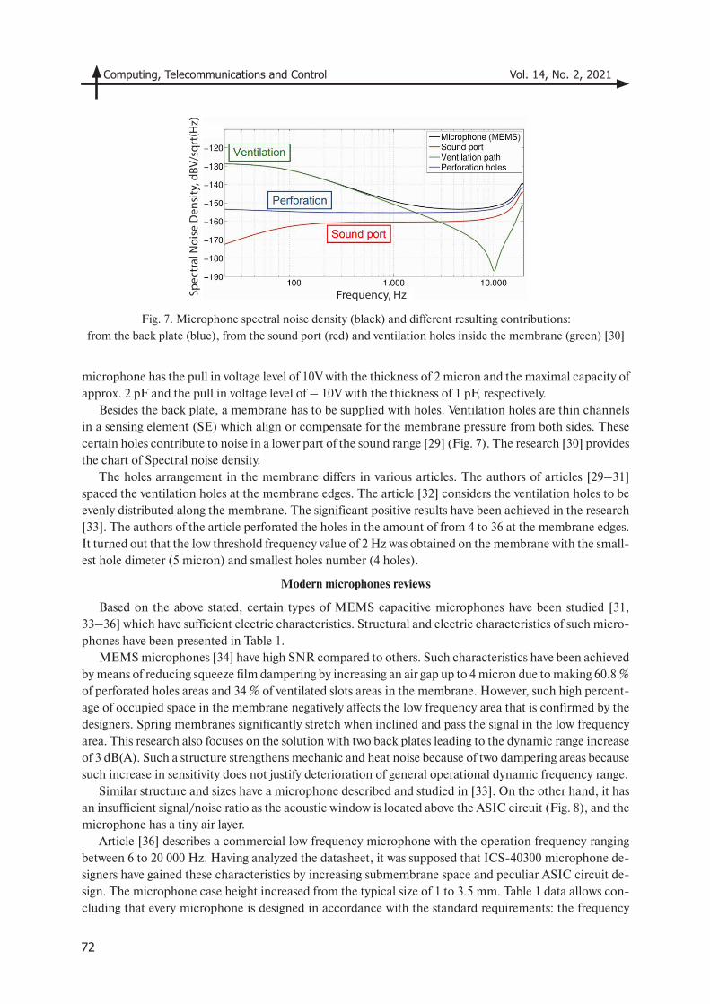
Computing, Telecommunications and Control Vol. 14, No. 2, 2021
72
Fig. 7. Microphone spectral noise density (black) and different resulting contributions:
from the back plate (blue), from the sound port (red) and ventilation holes inside the membrane (green) [30]
microphone has the pull in voltage level of 10V with the thickness of 2 micron and the maximal capacity of approx. 2 pF and the pull in voltage level of – 10V with the thickness of 1 pF, respectively.
Besides the back plate, a membrane has to be supplied with holes. Ventilation holes are thin channels in a sensing element (SE) which align or compensate for the membrane pressure from both sides. These certain holes contribute to noise in a lower part of the sound range [29] (Fig. 7). The research [30] provides the chart of Spectral noise density.
The holes arrangement in the membrane differs in various articles. The authors of articles [29–31] spaced the ventilation holes at the membrane edges. The article [32] considers the ventilation holes to be evenly distributed along the membrane. The significant positive results have been achieved in the research [33]. The authors of the article perforated the holes in the amount of from 4 to 36 at the membrane edges. It turned out that the low threshold frequency value of 2 Hz was obtained on the membrane with the small-est hole dimeter (5 micron) and smallest holes number (4 holes).
Modern microphones reviews
Based on the above stated, certain types of MEMS capacitive microphones have been studied [31, 33–36] which have sufficient electric characteristics. Structural and electric characteristics of such micro-phones have been presented in Table 1.
MEMS microphones [34] have high SNR compared to others. Such characteristics have been achieved by means of reducing squeeze film dampering by increasing an air gap up to 4 micron due to making 60.8 % of perforated holes areas and 34 % of ventilated slots areas in the membrane. However, such high percent-age of occupied space in the membrane negatively affects the low frequency area that is confirmed by the designers. Spring membranes significantly stretch when inclined and pass the signal in the low frequency area. This research also focuses on the solution with two back plates leading to the dynamic range increase of 3 dB(А). Such a structure strengthens mechanic and heat noise because of two dampering areas because such increase in sensitivity does not justify deterioration of general operational dynamic frequency range.
Similar structure and sizes have a microphone described and studied in [33]. On the other hand, it has an insufficient signal/noise ratio as the acoustic window is located above the ASIC circuit (Fig. 8), and the microphone has a tiny air layer.
Article [36] describes a commercial low frequency microphone with the operation frequency ranging between 6 to 20 000 Hz. Having analyzed the datasheet, it was supposed that ICS-40300 microphone de-signers have gained these characteristics by increasing submembrane space and peculiar ASIC circuit de-sign. The microphone case height increased from the typical size of 1 to 3.5 mm. Table 1 data allows con-cluding that every microphone is designed in accordance with the standard requirements: the frequency
Spec
tral
Noi
se D
ensi
ty, d
BV/s
qrt(
Hz)
Frequency, Hz
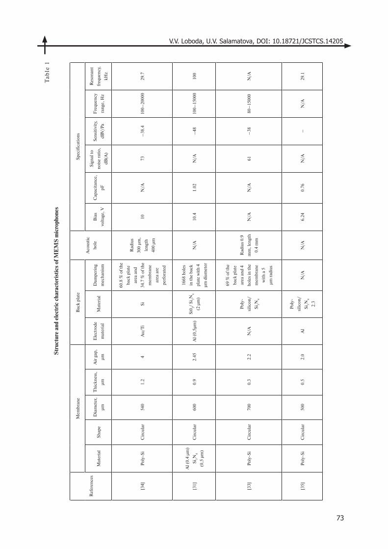
V.V. Loboda, U.V. Salamatova, DOI: 10.18721/JCSTCS.14205
73
Ta
ble
1
Str
uctu
re a
nd e
lect
ric
char
acte
rist
ics
of M
EM
S m
icro
phon
es
Ref
eren
ces
Mem
bran
eB
ack
plat
e
Aco
usti
c
hol
e
Spe
cifi
cati
ons
Mat
eria
lS
hap
eD
iam
eter
,
μm
Th
ickn
ess,
μm
Air
gap
,
μm
Ele
ctro
de
mat
eria
lM
ater
ial
Dam
peri
ng
mec
han
ism
Bia
s
volt
age,
V
Cap
acit
ance
,
pF
Sig
nal
to
noi
se r
atio
,
dB(A
)
Sen
siti
vity
,
dBV
/Pa
Fre
quen
cy
ran
ge, H
z
Res
onan
t
freq
uen
cy,
kHz
[34]
Pol
y-S
iC
ircu
lar
540
1.2
4A
u/T
iS
i
60.8
% o
f th
e
back
pla
te
area
an
d
34.7
% o
f th
e
mem
bran
e
area
are
perf
orat
ed
Rad
ius
300
μm,
len
gth
400
μm
10
N/A
73
–38
.410
0–20
000
29.7
[31]
Al (
0.4
μm)
Si 3N
4
(0,5
μm
)
Cir
cula
r60
00.
92.
45A
l (0,
5μm
)S
i02/
Si 3N
4
(2 μ
m)
1668
hol
es
in th
e ba
ck
plat
e w
ith
4
μm d
iam
eter
N/A
10.4
1.02
N/A
–48
100–
1500
010
0
[33]
Pol
y-S
iC
ircu
lar
700
0.3
2.2
N/A
Pol
y-
silic
on/
Si 3N
4
69 %
of t
he
back
pla
te
area
an
d 4
hol
es in
the
mem
bran
e
wit
h a
5
μm r
adiu
s
Rad
ius
0.9
mm
, len
gth
0.4
mm
N/A
N/A
61–
3880
–15
000
N/A
[35]
Pol
y-S
iC
ircu
lar
500
0.5
2.0
Al
Pol
y-
silic
on/
Si 3N
4
2.3
N/A
N/A
6.24
0.76
N/A
–N
/A29
.1
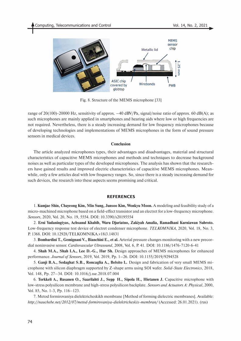
Computing, Telecommunications and Control Vol. 14, No. 2, 2021
74
range of 20(100)-20000 Hz, sensitivity of approx. –40 dBV/Pa, signal/noise ratio of approx. 60 dB(А); as such microphones are mainly applied in smartphones and hearing aids where low or high frequencies are not required. Nevertheless, there is a steady increasing demand for low frequency microphones because of developing technologies and implementations of MEMS microphones in the form of sound pressure sensors in medical devices.
Conclusion
The article analyzed microphones types, their advantages and disadvantages, material and structural characteristics of capacitive MEMS microphones and methods and techniques to decrease background noises as well as particular types of the developed microphones. The analysis has shown that the research-ers have gained results and improved electric characteristics of capacitive MEMS microphones. Mean-while, only a few articles deal with low frequency ranges. So, since there is a steady increasing demand for such devices, the research into these aspects seems promising and critical.
Fig. 8. Structure of the MEMS microphone [33]
REFERENCES
1. Kumjae Shin, Chayeong Kim, Min Sung, Junsoo Kim, Wonkyu Moon. A modeling and feasibility study of a
micro-machined microphone based on a field-effect transistor and an electret for a low-frequency microphone.
Sensors, 2020, Vol. 20, No. 19, 5554. DOI: 10.3390/s20195554
2. Erni Yudaningtyas, Achsanul Khabib, Waru Djuriatno, Zakiyah Amalia, Ramadhani Kurniawan Subroto.
Low-frequency response test device of electret condenser microphone. TELKOMNIKA, 2020, Vol. 18, No. 3,
P. 1368. DOI: 10.12928/TELKOMNIKA.v18i3.14831
3. Bombardini T., Gemignani V., Bianchini E., et al. Arterial pressure changes monitoring with a new precor-
dial noninvasive sensor. Cardiovascular Ultrasound, 2008, Vol. 6, P. 41. DOI: 10.1186/1476-7120-6-41
4. Shah M.A., Shah I.A., Lee D.-G., Hur Sh. Design approaches of MEMS microphones for enhanced
performance. Journal of Sensors, 2019, Vol. 2019, Pp. 1–26. DOI: 10.1155/2019/9294528
5. Ganji B.A., Sedaghat S.B., Roncaglia A., Belsito L. Design and fabrication of very small MEMS mi-
crophone with silicon diaphragm supported by Z-shape arms using SOI wafer. Solid-State Electronics, 2018,
Vol. 148, Pp. 27–34. DOI: 10.1016/j.sse.2018.07.004
6. Torkkeli A., Rusanen O., Saarilahti J., Seppä H., Sipola H., Hietanen J. Capacitive microphone with
low-stress polysilicon membrane and high-stress polysilicon backplate. Sensors and Actuators A: Physical, 2000,
Vol. 85, No. 1-3, Pp. 116–123.
7. Metod formirovaniya dielektricheskikh membrane [Method of forming dielectric membranes]. Available:
http://nauchebe.net/2012/07/metod-formirovaniya-dielektricheskix-membran/ (Accessed: 26.01.2021). (rus)
Metallic lid
V.V. Loboda, U.V. Salamatova, DOI: 10.18721/JCSTCS.14205
75
8. Amelichev V.V., Generalov S.S., Nikiforov S.V. Sozdaniye dielektricheskikh membran s nizkim urov-
nem mekhanicheskikh napryazheniy [Creation of dielectric membranes with a low level of mechanical
stress]. Novoye slovo v nauke: perspektivy razvitiya [A new word in science: development prospects], 2015, No. 4,
Pp. 127–128. (rus)
9. Shubham S. Silicon nitride corrugated membrane with high-width-aspect-ratio. Knowles Electronics,
2020.
10. Yooē I., Simē J., Yang S., Kim H. Development of capacitive MEMS microphone based on slit-edge for
high signal-to-noise ratio. IEEE Micro Electro Mechanical Systems (MEMS), 2018, Pp. 1072–1075.
11. Young Hwa Lee, Youngdo Jung, Jun-Hyuk Kwak, Shin Hur. Development of capacitive-type MEMS mi-
crophone with CMOS amplifying chip. International Journal of Precision Engineering and Manufacturing, 2014,
Vol. 15, No. 7, Pp. 1423–1427. DOI: 10.1007/s12541-014-0486-7
12. Sedighe Babaei Sedaghat, Bahram Azizollah Ganji. A novel MEMS capacitive microphone using spring-
type diaphragm. Microsystem Technologies, 2019, Vol. 25, No. 1, Pp. 217–224. DOI: 10.1007/s00542-018-
3951-x
13. Auliya R.Z., Ooi P.C., Mohd. Razip Wee M., et al. 3D finite element analysis of corrugated silicon
carbide membrane for ultrasonic MEMS microphone applications. Microsystem Technologies, 2020, Vol. 27,
Pp. 913–919. DOI: 10.1007/s00542-020-05006-1
14. Grigoryev D.M., Generalov S.S., Polomoshnov S.A., Nikiforov S.V., Amelichev V.V. Kondensatornyy
MEMS-mikrofon [Condenser MEMS microphone]. Mikroelektronika [Microelectronics], 2020, Vol. 49, No. 1,
Pp. 40–45. (rus) DOI: 10.31857/S0544126920010081
15. Vlasov A.I., Tsivinskaya T.A., Shakhnov V.A. Analiz vliyaniya formy membrany na mekhanicheskuyu
prochnost i stabilnost parametrov MEMS-sensorov davleniya [Analysis of the effect of membrane shape at me-
chanical strength and parameter stability of MEMS pressure sensors]. Problemy razrabotki perspektivnykh mikro-
i nanoelektronnykh sisitem [Problems of development of advanced micro-and nanoelectronic systems (MES)], 2016,
No. 4, Pp. 65–70. (rus)
16. Scheeper P. R., Olthuis W., Bergveld P. The design, fabrication, and testing of corrugated silicon nitride
diaphragms. Journal of Microelectromechanical Systems, 1994, Vol. 3, No. 1, Pp. 36–42. DOI:10.1109/84.285722
17. Siti Aisyah Zawawi, Azrul Azlan Hamzah, Burhanuddin Yeop Majlis, Faisal Mohd-Yasin. A review of
MEMS capacitive microphones. Micromachines, 2020, Vol. 11, No. 5. DOI:10.3390/mi11050484
18. Yew M.C., et al. A study of residual stress effects on CMOS-MEMS microphone technology. 2009 4th
International Microsystems, Packaging, Assembly and Circuits Technology Conference. IEEE, 2009, Pp. 323–326.
19. Kressmann R., Klaiber M., Hess G. Silicon condenser microphones with corrugated silicon oxide/nitride
electret membranes. Sensors and Actuators A: Physical, 2002, Vol. 100, No. 2-3, Pp. 301–309. DOI:10.1016/
S0924-4247(02)00137-1
20. Fu M., Dehe A., Lerch R. Analytical analysis and finite element simulation of advanced membranes for
silicon microphones. IEEE Sensors Journal, 2005, Vol. 5, No. 5, Pp. 857–863.
21. Lapadatu D., et al. Corrugated silicon nitride membranes as suspensions in micromachined silicon ac-
celerometers. Journal of Micromechanics and Microengineering, 1996, Vol. 6, No. 1, P. 73.
22. Grigoryev D.M., Godovitsyn I.V., Amelichev V.V., Generalov S.S. Raschet AChKh MEMS-mikrofona s
pomoshchyu konechno-elementnogo modelirovaniya [Calculation of the frequency response of a MEMS mi-
crophone using finite element modeling]. Mikroelektronika [Microelectronics], 2018, No. 3, Pp. 238–243. (rus).
DOI: 10.7868/S0544126918030080
23. Tan C.W., Miao J. Analytical modeling for bulk-micromachined condenser microphones. The Journal of
the Acoustical Society of America, 2006, Vol. 120, No. 2, Pp. 750–761. DOI: 10.1121/1.2216561
24. Infineon Technologies AG, IM69D120. Available: https://www.infineon.com/dgdl/Infineon-IM69D120-
DataSheet-v01_00-EN.pdf (Accessed: 21.06.2021).
25. 1/f-shum: ponimaniye i metody borby. Available: https://spb.terraelectronica.ru/news/6096 (Accessed:
21.06.2021). (rus)
Computing, Telecommunications and Control Vol. 14, No. 2, 2021
76
Received 15.06.2021.
СПИСОК ЛИТЕРАТУРЫ
1. Kumjae Shin, Chayeong Kim, Min Sung, Junsoo Kim, Wonkyu Moon. A modeling and feasibility study of a
micro-machined microphone based on a field-effect transistor and an electret for a low-frequency microphone
// Sensors. 2020. Vol. 20. No. 19. P. 5554. DOI: 10.3390/s20195554
2. Erni Yudaningtyas, Achsanul Khabib, Waru Djuriatno, Zakiyah Amalia, Ramadhani Kurniawan Subroto.
Low-frequency response test device of electret condenser microphone // TELKOMNIKA. 2020. Vol. 18. No. 3.
P. 1368. DOI: 10.12928/TELKOMNIKA.v18i3.14831
3. Bombardini T., Gemignani V., Bianchini E., et al. Arterial pressure changes monitoring with a new precor-
dial noninvasive sensor // Cardiovascular ultrasound. 2008. Vol. 6. P. 41. DOI: 10.1186/1476-7120-6-41
4. Shah M.A., Shah I.A., Lee D.-G., Hur Sh. Design approaches of MEMS microphones for enhanced
performance // J. of Sensors. 2019. Vol. 2019. Pp. 1–26. DOI: 10.1155/2019/9294528
5. Ganji B.A., Sedaghat S.B., Roncaglia A., Belsito L. Design and fabrication of very small MEMS micro-
phone with silicon diaphragm supported by Z-shape arms using SOI wafer // Solid-State Electronics. 2018.
Vol. 148. Pp. 27–34. DOI: 10.1016/j.sse.2018.07.004
6. Torkkeli A., Rusanen O., Saarilahti J., Seppä H., Sipola H., Hietanen J. Capacitive microphone with low-
stress polysilicon membrane and high-stress polysilicon backplate // Sensors and Actuators A: Physical. 2000.
Vol. 85. No. 1-3. Pp. 116–123.
26. Homentcovschi D., Miles R.N. Viscous damping of perforated planar micromechanical structures. Sen-
sors and Actuators. A, Physical, 2005, Vol. 119, No. 2, Pp. 544–552. DOI: 10.1016/j.sna.2004.10.032
27. Brace E., et al. Impact of support material deformation in MEMS bulk micromachined diaphragm pres-
sure sensors. Journal of Micromechanics and Microengineering, 2021, Vol. 31, No. 5, P. 055001.
28. Grigoryev D.M., Godovitsyn I.V., Amelichev V.V., Generalov S.S., Polomoshnov S.A. Ispolzovaniye
konechno-elementnogo modelirovaniya dlya rascheta CV-kharakteristiki kondensatornogo MEMS-mikrofona
[Using finite element modeling to calculate the CV characteristics of a condenser MEMS microphone]. Mikro-
elektronika [Microelectronics], 2017, Vol. 46, No. 6, Pp. 431–439. (rus) DOI: 10.7868/S0544126917060047
29. Nicollini G., Devecchi D. MEMS capacitive microphones: acoustical, electrical, and hidden thermal-re-
lated issues. IEEE Sensors Journal, 2018, Vol. 18, No. 13, Pp. 5386–5394.
30. Kuenzig T., et al. Performance and noise analysis of capacitive silicon microphones using tailored sys-
tem-level simulation. Proceedings of the 18th International Conference on Solid-State Sensors, Actuators and Mi-
crosystems (TRANSDUCERS), IEEE, 2015, Pp. 2192–2195.
31. Lee J., Je C.H., Yang W.S., Kim J. Structure-based equivalent circuit modeling of a capacitive-type
MEMS microphone. Internat. Symp. on Communications and Information Technologies (ISCIT). IEEE, 2012,
Pp. 228–233.
32. Lall P., Abrol A., Locker D. Effects of sustained exposure to temperature and humidity on the reliability
and performance of MEMS microphone. International Electronic Packaging Technical Conference and Exhibi-
tion. American Society of Mechanical Engineers, 2017, Vol. 58097, V001T01A022.
33. Dehé A., et al. Design of a poly silicon MEMS microphone for high signal-to-noise ratio. 2013 Proceed-
ings of the European Solid-State Device Research Conference (ESSDERC), IEEE, 2013, Pp. 292–295.
34. Byung-Hun Kim, Hwa-Sun Lee. Acoustical-thermal noise in a capacitive MEMS microphone. IEEE
Sensors Journal, 2015, Vol. 15, No. 12, Pp. 6853–6860.
35. Chang Han Je, Ju Hyun Jeon, Sung Q. Lee, Woo Seok Yang. MEMS capacitive microphone with du-
al-anchored membrane. Proceedings, 2017, Vol. 1, No. 4, P. 342. DOI: 10.3390/proceedings1040342
36. Lewis J. Microphone specifications explained. Analog Devices. Application Note AN-1112, 2011.
V.V. Loboda, U.V. Salamatova, DOI: 10.18721/JCSTCS.14205
77
7. Метод формирования диэлектрических мембран // URL: http://nauchebe.net/2012/07/metod-
formirovaniya-dielektricheskix-membran/ (Дата обращения: 26.01.2021).
8. Амеличев В.В., Генералов С.С., Никифоров С.В. Создание диэлектрических мембран с низким уров-
нем механических напряжений // Новое слово в науке: перспективы развития. 2015. 4. С. 127–128.
9. Shubham S. Silicon nitride corrugated membrane with high-width-aspect-ratio // Knowles Electronics.
2020.
10. Yooē I., Simē J., Yang S., Kim H. Development of capacitive MEMS microphone based on slit-edge for
high signal-to-noise ratio. IEEE Micro Electro Mechanical Systems (MEMS), 2018, Pp. 1072–1075.
11. Young Hwa Lee, Youngdo Jung, Jun-Hyuk Kwak, Shin Hur. Development of capacitive-type MEMS
microphone with CMOS amplifying chip // Internat. J. of Precision Engineering and Manufacturing. 2014.
Vol. 15. No. 7. Pp. 1423–1427. DOI: 10.1007/s12541-014-0486-7
12. Sedighe Babaei Sedaghat, Bahram Azizollah Ganji. A novel MEMS capacitive microphone using spring-
type diaphragm // Microsystem Technologies. 2019. Vol. 25. No. 1. Pp. 217–224. DOI: 10.1007/s00542-018-
3951-x
13. Auliya R.Z., Ooi P.C., Mohd. Razip Wee M., et al. 3D finite element analysis of corrugated silicon car-
bide membrane for ultrasonic MEMS microphone applications // Microsystem Technologies. 2020. Vol. 27.
Pp. 913–919. DOI: 10.1007/s00542-020-05006-1
14. Григорьев Д.М., Генералов С.С., Поломошнов С.А., Никифоров С.В., Амеличев В.В. Конденса-
торный МЭМС-микрофон // Микроэлектроника. 2020. T. 49. 1. C. 40–45. DOI: 10.31857/S054412-
6920010081
15. Власов А.И., Цивинская Т.А., Шахнов В.А. Анализ влияния формы мембраны на механическую
прочность и стабильность параметров МЭМС-сенсоров давления // Проблемы разработки перспек-
тивных микро- и наноэлектронных сиситем. 2016. . С. 65–70.
16. Scheeper P. R., Olthuis W., Bergveld P. The design, fabrication, and testing of corrugated silicon nitride
diaphragms // J. of Microelectromechanical Systems. 1994. Vol. 3. No. 1. Pp. 36–42. DOI:10.1109/84.285722
17. Siti Aisyah Zawawi, Azrul Azlan Hamzah, Burhanuddin Yeop Majlis, Faisal Mohd-Yasin. A review of
MEMS capacitive microphones // Micromachines. 2020. Vol. 11. No. 5. DOI: 10.3390/mi11050484
18. Yew M.C., et al. A study of residual stress effects on CMOS-MEMS microphone technology // 2009 4th
International. Microsystems, Packaging, Assembly and Circuits Technology Conf. IEEE, 2009. Pp. 323–326.
19. Kressmann R., Klaiber M., Hess G. Silicon condenser microphones with corrugated silicon oxide/nitride
electret membranes // Sensors and Actuators A: Physical. 2002. Vol. 100. No. 2-3. Pp. 301–309. DOI:10.1016/
S0924-4247(02)00137-1
20. Fu M., Dehe A., Lerch R. Analytical analysis and finite element simulation of advanced membranes for
silicon microphones // IEEE Sensors Journal. 2005. Vol. 5. No. 5. Pp. 857–863.
21. Lapadatu D., et al. Corrugated silicon nitride membranes as suspensions in micromachined silicon ac-
celerometers // J. of Micromechanics and Microengineering. 1996. Vol. 6. No. 1. P. 73.
22. Григорьев Д.М., Годовицын И.В., Амеличев В.В., Генералов С.С. Расчет АЧХ МЭМС-микрофона
с помощью конечно-элементного моделирования // Микроэлектроника. 2018. 3. C. 238–243. DOI:
10.7868/S0544126918030080
23. Tan C.W., Miao J. Analytical modeling for bulk-micromachined condenser microphones // The Journal
of the Acoustical Society of America. 2006. Vol. 120. No. 2. Pp. 750–761. DOI: 10.1121/1.2216561
24. Infineon Technologies AG, IM69D120 // URL: https://www.infineon.com/dgdl/Infineon-IM69D120-
DataSheet-v01_00-EN.pdf (Дата обращения: 21.06.2021).
25. 1/f-шум: понимание и методы борьбы // URL: https://spb.terraelectronica.ru/news/6096 (Дата об-
ращения: 21.06.2021).
26. Homentcovschi D., Miles R.N. Viscous damping of perforated planar micromechanical structures //
Sensors and Actuators. A, Physical. 2005. Vol. 119. No. 2. Pp. 544–552. DOI: 10.1016/j.sna.2004.10.032
Computing, Telecommunications and Control Vol. 14, No. 2, 2021
78
Статья поступила в редакцию 15.06.2021.
THE AUTHORS / СВЕДЕНИЯ ОБ АВТОРАХ
Loboda Vera V.Лобода Вера ВладимировнаE-mail: [email protected]
Salamatova Ulyana V.Саламатова Ульяна ВячеславовнаE-mail: [email protected]
© Санкт-Петербургский политехнический университет Петра Великого, 2021
27. Brace E., et al. Impact of support material deformation in MEMS bulk micromachined diaphragm pres-
sure sensors // J. of Micromechanics and Microengineering. 2021. Vol. 31. No. 5. P. 055001.
28. Григорьев Д.М., Годовицын И.В., Амеличев В.В., Генералов С.С., Поломошнов С.А. Использова-
ние конечно-элементного моделирования для расчета CV-характеристики конденсаторного МЭМС-
микрофона // Микроэлектроника. 2017. Т. 46. 6. С. 431–439. DOI: 10.7868/S0544126917060047
29. Nicollini G., Devecchi D. MEMS capacitive microphones: Acoustical, electrical, and hidden thermal-re-
lated issues // IEEE Sensors Journal. 2018. Vol. 18. No. 13. Pp. 5386–5394.
30. Kuenzig T., et al. Performance and noise analysis of capacitive silicon microphones using tailored sys-
tem-level simulation // Proc. of the 18th Internat. Conf. on Solid-State Sensors, Actuators and Microsystems.
IEEE, 2015. Pp. 2192–2195.
31. Lee J., Je C.H., Yang W.S., Kim J. Structure-based equivalent circuit modeling of a capacitive-type
MEMS microphone // Internat. Symp. on Communications and Information Technologies (ISCIT). IEEE.
2012. Pp. 228–233.
32. Lall P., Abrol A., Locker D. Effects of sustained exposure to temperature and humidity on the reliability
and performance of MEMS microphone // Internat. Electronic Packaging Technical Conf. and Exhibition.
American Society of Mechanical Engineers. 2017. Vol. 58097. A. V001T01A022.
33. Dehé A., et al. Design of a poly silicon MEMS microphone for high signal-to-noise ratio // 2013 Proc.
of the European Solid-State Device Research Conf. IEEE, 2013. Pp. 292–295.
34. Byung-Hun Kim, Hwa-Sun Lee. Acoustical-thermal noise in a capacitive MEMS microphone // IEEE
Sensors J. 2015. Vol. 15. No. 12. Pp. 6853–6860.
35. Chang Han Je, Ju Hyun Jeon, Sung Q. Lee, Woo Seok Yang. MEMS capacitive microphone with du-
al-anchored membrane // Proc. 2017. Vol. 1. No. 4. P. 342. DOI: 10.3390/proceedings1040342
36. Lewis J. Microphone specifications explained // Analog Devices. Application Note AN-1112. 2011.
A.T. Tulaev, A.V. Styazhkina, A.S. Kozlov, Ya.V. Belyaev, DOI: 10.18721/JCSTCS.14206
79
DOI: 10.18721/JCSTCS.14206УДК 531.383
MICROMECHANICAL SENSORS DESIGN METHOD BASED ON SYSTEM-LEVEL MODELING
A.T. Tulaev, A.V. Styazhkina, A.S. Kozlov, Ya.V. BelyaevConcern CSRI Elektropribor, JSC,
St. Petersburg, Russian Federation
This paper proposes a design method for micromechanical inertial sensors with force feedback electromechanical loop with delta-sigma modulator. Development of such sensors requires application of modern design methods, including modeling at system level, model refinement based on results of finite element modeling and modeling of individual electronic blocks at circuit level, as well as implementation of a digital twin based on results of an experimental study of sensors samples. Such a complex approach to sensor design is caused by high requirements to sensor characteristics (both in terms of dynamic range and accuracy), the need to consider the impact of external factors and the various physics to describe the processes, the impossibility of rapid prototyping, the influence of technological process parameters on sensor characteristics, etc. In this regard, this paper proposes a comprehensive method for the design of micromechanical sensors based on the construction of the system model. This paper represents the results of an experimental study of the force feedback type sensor using the proposed method.
Keywords: micromechanical sensor, MEMS, delta-sigma modulator, system level model, digital twin.
Citation: Tulaev A.T., Styazhkina A.V., Kozlov A.S., Belyaev Ya.V. Micromechanical sensors design method based on system-level modeling. Computing, Telecommunications and Control, 2021, Vol. 14, No. 2, Pp. 79–92. DOI: 10.18721/JCST-CS.14206
This is an open access article under the CC BY-NC 4.0 license (https://creativecommons.org/licenses/by-nc/4.0/).
МЕТОДИКА ПРОЕКТИРОВАНИЯ МИКРОМЕХАНИЧЕСКОГО ДАТЧИКА НА ОСНОВЕ КОМПЛЕКСНОЙ СИСТЕМНОЙ МОДЕЛИ
А.Т. Тулаев, А.В. Стяжкина, А.С. Козлов, Я.В. БеляевЦНИИ «Электроприбор»,
Санкт-Петербург, Российская Федерация
Предложена методика проектирования микромеханических инерциальных датчиков компенсационного типа, в контуре управления которых применен дельта-сигма модулятор. Разработка таких датчиков требует современных методов проектирования, включающих мо-делирование на системном уровне, уточнение модели по результатам конечно-элементного моделирования и моделирования отдельных блоков контура управления на схемотехниче-ском уровне, а также реализацию цифрового двойника по результатам экспериментального исследования образцов. Такой комплексный подход к проектированию обусловлен высоки-ми требованиями к характеристикам датчика (как в части динамического диапазона, так и в части точностных характеристик), необходимостью учета различных физик для описания процессов, необходимостью оценки влияния внешних воздействующих факторов, невоз-можностью проведения быстрого макетирования, необходимостью учета влияния на ха-рактеристики датчика параметров технологического процесса и др. В связи с этим в статье предложена комплексная методика проектирования микромеханических датчиков на ос-нове системной модели. Приведены результаты экспериментального исследования датчика компенсационного типа с применением предложенной методики.
Computing, Telecommunications and Control Vol. 14, No. 2, 2021
80
Introduction
Due to their small size and power consumption, as well as their low cost in mass production, micro-electromechanical sensors (MEMS) are an integral part of modern small-size navigation and motion control systems [1, 2]. Inertial MEMS include micromechanical accelerometers (MMA) and gyro-scopes (MМG), designed to determine the linear acceleration and angular velocity of the object, re-spectively. The use in navigation and motion control systems imposes strict requirements on MMAs and MMGs [1, 2]:
- wide measurement range from ± 200 to ± 7000°/s – for MMG and from ± 2 to ± 50g – for MMA;- low non-linearity of the sensor output – at level of 0.01 %;- wide dynamic range – more than 100 dB;- high temporal stability of output signal – at 5°/h for MMG and 0.01 mg for MMA- robustness to external influences (temperature variations from minus 60 to plus 85°C, impact and
vibration, etc.) – at 100°/h for MMG and 1 mg for MMA.Such requirements can be achieved by applying comprehensive solutions at the design level:- by using multiple proof mass sensing elements [3–6];- by utilizing specialized integrated circuits, in particular compensation circuits with a delta-sigma
modulator in the control loop [7–17];- by using temperature stabilization systems, etc. Complication of inertial MEMS architecture, impossibility of fast prototyping, necessity of simulta-
neous modelling of blocks of integrated circuit and sensing element, the need to consider influence of external influencing factors and different physics for describing processes, as well as influence of tech-nological process parameters require to design MEMS based on an accurate mathematical model. The existing design methodologies and mathematical models of inertial MEMS they are based on [18, 19] have a number of drawbacks:
- the electronic blocks processing output signal are not considered at all or considered in a simplified manner;
- the sensing element is represented by lumped parameters (elastic rigid suspension stiffness, electrode structure capacitance), determined separately analytically or by finite element analysis;
- the model does not take into account experimental data.In this regard, this paper proposes a comprehensive methodology for designing capacitive inertial
MEMS based on the system model that takes into account the main electronic blocks of output signal processing, the results of coupled finite-element modelling of the sensing element and the results of experimental studies. Thus, a prototype of a digital twin sensor is implemented in the course of the design, which allows increasing its accuracy. The methodology is considered on the example of MMA and MMG developed by CSRI Elektropribor, JSC.
Object of study
The main parts of capacitive MMA and MMG are:- a sensing element (SE), designed to convert the input acceleration into a change in capacitance;
Ключевые слова: микромеханический датчик, МЭМС, дельта-сигма модулятор, системная модель, цифровой двойник.
Ссылка при цитировании: Tulaev A.T., Styazhkina A.V., Kozlov A.S., Belyaev Ya.V. Microme-chanical sensors design method based on system-level modeling // Computing, Telecommunica-tions and Control. 2021. Vol. 14. No. 2. Pp. 79–92. DOI: 10.18721/JCSTCS.14206
Cтатья открытого доступа, распространяемая по лицензии CC BY-NC 4.0 (https://creative-commons.org/licenses/by-nc/4.0/).
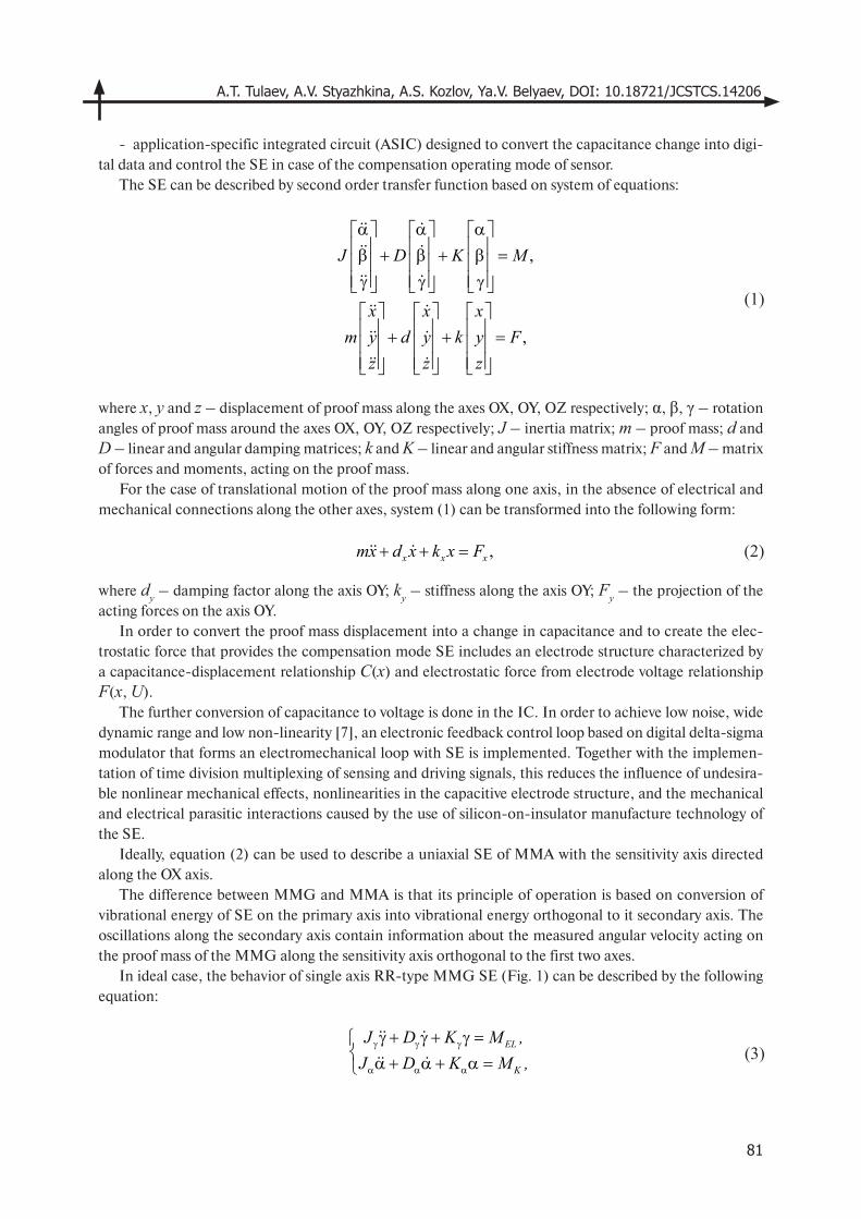
A.T. Tulaev, A.V. Styazhkina, A.S. Kozlov, Ya.V. Belyaev, DOI: 10.18721/JCSTCS.14206
81
- application-specific integrated circuit (ASIC) designed to convert the capacitance change into digi-tal data and control the SE in case of the compensation operating mode of sensor.
The SE can be described by second order transfer function based on system of equations:
where x, y and z – displacement of proof mass along the axes OX, OY, OZ respectively; α, β, γ – rotation angles of proof mass around the axes OX, OY, OZ respectively; J – inertia matrix; m – proof mass; d and D – linear and angular damping matrices; k and K – linear and angular stiffness matrix; F and М – matrix of forces and moments, acting on the proof mass.
For the case of translational motion of the proof mass along one axis, in the absence of electrical and mechanical connections along the other axes, system (1) can be transformed into the following form:
where dy – damping factor along the axis OY; ky – stiffness along the axis OY; Fy – the projection of the acting forces on the axis OY.
In order to convert the proof mass displacement into a change in capacitance and to create the elec-trostatic force that provides the compensation mode SE includes an electrode structure characterized by a capacitance-displacement relationship C(x) and electrostatic force from electrode voltage relationship F(x, U).
The further conversion of capacitance to voltage is done in the IC. In order to achieve low noise, wide dynamic range and low non-linearity [7], an electronic feedback control loop based on digital delta-sigma modulator that forms an electromechanical loop with SE is implemented. Together with the implemen-tation of time division multiplexing of sensing and driving signals, this reduces the influence of undesira-ble nonlinear mechanical effects, nonlinearities in the capacitive electrode structure, and the mechanical and electrical parasitic interactions caused by the use of silicon-on-insulator manufacture technology of the SE.
Ideally, equation (2) can be used to describe a uniaxial SE of MMA with the sensitivity axis directed along the OX axis.
The difference between MMG and MMA is that its principle of operation is based on conversion of vibrational energy of SE on the primary axis into vibrational energy orthogonal to it secondary axis. The oscillations along the secondary axis contain information about the measured angular velocity acting on the proof mass of the MMG along the sensitivity axis orthogonal to the first two axes.
In ideal case, the behavior of single axis RR-type MMG SE (Fig. 1) can be described by the following equation:
,
,
J D K M
x x xm y d y k y F
z z z
α α α β + β + β = γ γ γ + + =
(1)
,x x xmx d x k x F+ + = (2)
EL
K
J D K M ,J D K M ,
γ γ γ
α α α
γ + γ + γ = α + α + α =
(3)
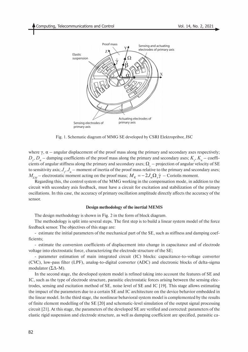
Computing, Telecommunications and Control Vol. 14, No. 2, 2021
82
where γ, α – angular displacement of the proof mass along the primary and secondary axes respectively; Dγ, Dα – damping coefficients of the proof mass along the primary and secondary axes; Kγ, Kα – coeffi-cients of angular stiffness along the primary and secondary axes; Ωy – projection of angular velocity of SE to sensitivity axis; Jγ, Jα – moment of inertia of the proof mass relative to the primary and secondary axes; MEM – electrostatic moment acting on the proof mass; – Coriolis moment.
Regarding this, the control system of the MMG working in the compensation mode, in addition to the circuit with secondary axis feedback, must have a circuit for excitation and stabilization of the primary oscillations. In this case, the accuracy of primary oscillation amplitude directly affects the accuracy of the sensor.
Design methodology of the inertial MEMS
The design methodology is shown in Fig. 2 in the form of block diagram.The methodology is split into several steps. The first step is to build a linear system model of the force
feedback sensor. The objectives of this stage are: - estimate the initial parameters of the mechanical part of the SE, such as stiffness and damping coef-
ficients;- estimate the conversion coefficients of displacement into change in capacitance and of electrode
voltage into electrostatic force, characterizing the electrode structure of the SE;- parameter estimation of main integrated circuit (IC) blocks: capacitance-to-voltage converter
(CVC), low-pass filter (LPF), analog-to-digital converter (ADC) and electronic blocks of delta-sigma modulator (ΣΔ-M).
In the second stage, the developed system model is refined taking into account the features of SE and IC, such as the type of electrode structure, parasitic electrostatic forces arising between the sensing elec-trodes, sensing and excitation method of SE, noise level of SE and IC [19]. This stage allows estimating the impact of the parameters due to a certain SE and IC architecture on the device behavior embedded in the linear model. In the third stage, the nonlinear behavioral system model is complemented by the results of finite element modelling of the SE [20] and schematic-level simulation of the output signal processing circuit [21]. At this stage, the parameters of the developed SE are verified and corrected: parameters of the elastic rigid suspension and electrode structure, as well as damping coefficient are specified, parasitic ca-
Fig. 1. Schematic diagram of MMG SE developed by CSRI Elektropribor, JSC
2K yM Jα= − Ω γ
Elasticsuspension
Proof mass
Sensing electrodes ofprimary axis
Actuating electrodes ofprimary axis
Sensing and actuatingelectrodes of primary axis
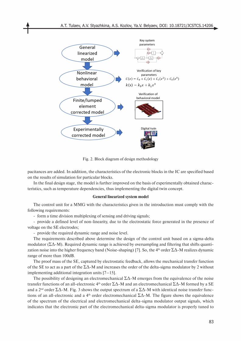
A.T. Tulaev, A.V. Styazhkina, A.S. Kozlov, Ya.V. Belyaev, DOI: 10.18721/JCSTCS.14206
83
Fig. 2. Block diagram of design methodology
pacitances are added. In addition, the characteristics of the electronic blocks in the IC are specified based on the results of simulation for particular blocks.
In the final design stage, the model is further improved on the basis of experimentally obtained charac-teristics, such as temperature dependencies, thus implementing the digital twin concept.
General linearized system model
The control unit for a MMG with the characteristics given in the introduction must comply with the following requirements:
- form a time division multiplexing of sensing and driving signals;- provide a defined level of non-linearity, due to the electrostatic force generated in the presence of
voltage on the SE electrodes;- provide the required dynamic range and noise level.The requirements described above determine the design of the control unit based on a sigma-delta
modulator (ΣΔ-M). Required dynamic range is achieved by oversampling and filtering that shifts quanti-zation noise into the higher frequency band (Noise-shaping) [7]. So, the 4th order ΣΔ-M realizes dynamic range of more than 100dB.
The proof mass of the SE, captured by electrostatic feedback, allows the mechanical transfer function of the SE to act as a part of the ΣΔ-M and increases the order of the delta-sigma modulator by 2 without implementing additional integration units [7–15].
The possibility of designing an electromechanical ΣΔ-M emerges from the equivalence of the noise transfer functions of an all-electronic 4th order ΣΔ-M and an electromechanical ΣΔ-M formed by a SE and a 2nd order ΣΔ-M. Fig. 3 shows the output spectrum of a ΣΔ-M with identical noise transfer func-tions of an all-electronic and a 4th order electromechanical ΣΔ-M. The figure shows the equivalence of the spectrum of the electrical and electromechanical delta-sigma modulator output signals, which indicates that the electronic part of the electromechanical delta-sigma modulator is properly tuned to
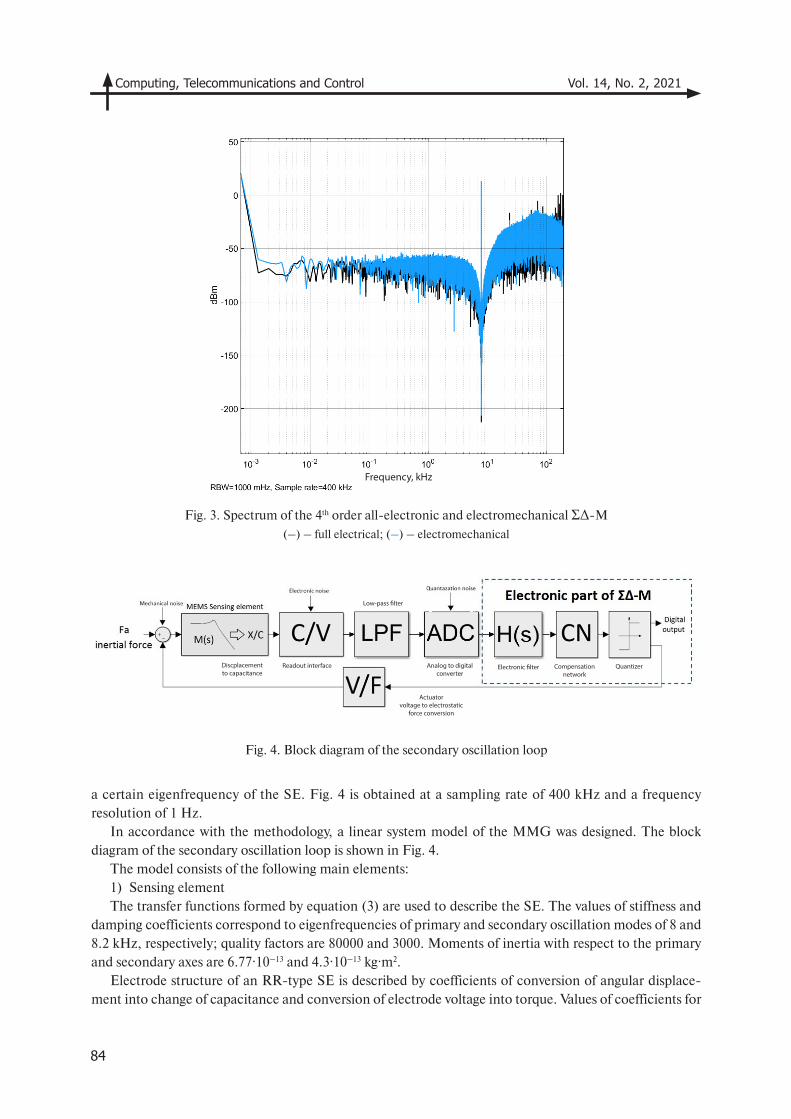
Computing, Telecommunications and Control Vol. 14, No. 2, 2021
84
Fig. 3. Spectrum of the 4th order all-electronic and electromechanical ΣΔ-M
(–) – full electrical; (–) – electromechanical
Fig. 4. Block diagram of the secondary oscillation loop
a certain eigenfrequency of the SE. Fig. 4 is obtained at a sampling rate of 400 kHz and a frequency resolution of 1 Hz.
In accordance with the methodology, a linear system model of the MMG was designed. The block diagram of the secondary oscillation loop is shown in Fig. 4.
The model consists of the following main elements:1) Sensing elementThe transfer functions formed by equation (3) are used to describe the SE. The values of stiffness and
damping coefficients correspond to eigenfrequencies of primary and secondary oscillation modes of 8 and 8.2 kHz, respectively; quality factors are 80000 and 3000. Moments of inertia with respect to the primary and secondary axes are 6.77∙10–13 and 4.3∙10–13 kg∙m2.
Electrode structure of an RR-type SE is described by coefficients of conversion of angular displace-ment into change of capacitance and conversion of electrode voltage into torque. Values of coefficients for
Frequency, kHz
Actuatorvoltage to electrostatic
force conversion
Readout interfaceDiscplacementto capacitance
Analog to digitalconverter
Low-pass filter
Electronic filter QuantizerCompensationnetwork
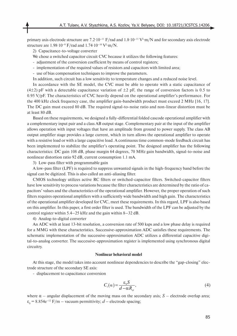
A.T. Tulaev, A.V. Styazhkina, A.S. Kozlov, Ya.V. Belyaev, DOI: 10.18721/JCSTCS.14206
85
primary axis electrode structure are 7.2∙10–11 F/rad and 1.8∙10–11 V2∙m/N and for secondary axis electrode structure are 1.98∙10–9 F/rad and 1.74∙10–10 V2∙m/N.
2) Capacitance-to-voltage converter We chose a switched capacitor circuit CVC because it utilizes the following features:- adjustment of the conversion coefficient by means of control registers;- implementation of the required values of resistors and capacitors with limited area;- use of bias compensation techniques to improve the parameters.In addition, such circuit has a low sensitivity to temperature changes and a reduced noise level.In accordance with the SE model, the CVC must be able to operate with a static capacitance of
(4±2) pF with a detectable capacitance variation of ±2 pF, the range of conversion factors is 0.5 to 0.95 V/pF. The characteristics of CVC heavily depend on the operational amplifier’s performance. For the 400 kHz clock frequency case, the amplifier gain-bandwidth product must exceed 2 MHz [16, 17]. The DC gain must exceed 80 dB. The required signal-to-noise ratio and non-linear distortion must be at least 80 dB.
Based on these requirements, we designed a fully-differential folded cascode operational amplifier with a complementary input pair and a class AB output stage. Complementary pair at the input of the amplifier allows operation with input voltages that have an amplitude from ground to power supply. The class AB output amplifier stage provides a large current, which in turn allows the operational amplifier to operate with a resistive load or with a large capacitive load. A continuous time common-mode feedback circuit has been implemented to stabilize the amplifier’s operating point. The designed amplifier has the following characteristics: DC gain 108 dB, phase margin 64 degrees, 70 MHz gain bandwidth, signal-to-noise and nonlinear distortion ratio 92 dB, current consumption 1.1 mA.
3) Low-pass filter with programmable gainA low-pass filter (LPF) is required to suppress unwanted signals in the high-frequency band before the
signal can be digitized. This is also called an anti-aliasing filter.CMOS technology utilizes active RC filters or switched-capacitor filters. Switched-capacitor filters
have low sensitivity to process variations because the filter characteristics are determined by the ratio of ca-pacitors’ values and the characteristics of the operational amplifier. However, the proper operation of such filters requires operational amplifiers with a sufficiently wide bandwidth and high gain. The characteristics of the operational amplifier developed for CVC, meet these requirements. In this regard, LPF is also based on this amplifier. In this paper, a first order filter is used. The bandwidth of the LPF can be adjusted by the control register within 5.4–25 kHz and the gain within 8–32 dB.
4) Analog-to-digital converterAn ADC with at least 13-bit resolution, a conversion rate of 500 ksps and a low phase delay is required
for a MMG with these characteristics. Successive-approximation ADC satisfies these requirements. The schematic implementation of the successive-approximation ADC utilizes a differential capacitive digi-tal-to-analog converter. The successive-approximation register is implemented using synchronous digital circuitry.
Nonlinear behavioral model
At this stage, the model takes into account nonlinear dependencies to describe the “gap-closing” elec-trode structure of the secondary SE axis:
- displacement to capacitance conversion
where α – angular displacement of the moving mass on the secondary axis; S – electrode overlap area; ε
0 = 8.854e–12 F/m – vacuum permittivity; d – electrode spacing;
( ) 01 ,
cp
SCd R
αε=−α
(4)
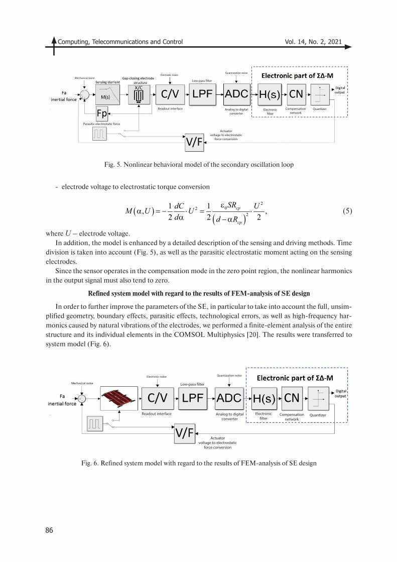
Computing, Telecommunications and Control Vol. 14, No. 2, 2021
86
- electrode voltage to electrostatic torque conversion
where U – electrode voltage.In addition, the model is enhanced by a detailed description of the sensing and driving methods. Time
division is taken into account (Fig. 5), as well as the parasitic electrostatic moment acting on the sensing electrodes.
Since the sensor operates in the compensation mode in the zero point region, the nonlinear harmonics in the output signal must also tend to zero.
Refined system model with regard to the results of FEM-analysis of SE design
In order to further improve the parameters of the SE, in particular to take into account the full, unsim-plified geometry, boundary effects, parasitic effects, technological errors, as well as high-frequency har-monics caused by natural vibrations of the electrodes, we performed a finite-element analysis of the entire structure and its individual elements in the COMSOL Multiphysics [20]. The results were transferred to system model (Fig. 6).
Fig. 5. Nonlinear behavioral model of the secondary oscillation loop
Fig. 6. Refined system model with regard to the results of FEM-analysis of SE design
(5)( )( )
202
21 1, ,2 2 2
cp
cp
SRdC UM U Ud d R
εα = − ⋅ = ⋅
α −α
Actuatorvoltage to electrostatic
force conversion
Analog to digitalconverter
Electronicfilter
Compensationnetwork
Quantizer
Low-pass filter
Readout interface
Low-pass filter
Readout interface
Parasitic electrostatic force
Analog to digitalconverter
Actuatorvoltage to electrostatic
force conversion
QuantizerCompensationnetwork
Electronicfilter
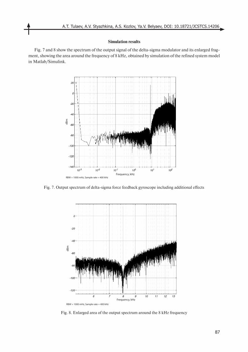
A.T. Tulaev, A.V. Styazhkina, A.S. Kozlov, Ya.V. Belyaev, DOI: 10.18721/JCSTCS.14206
87
Simulation results
Fig. 7 and 8 show the spectrum of the output signal of the delta-sigma modulator and its enlarged frag-ment, showing the area around the frequency of 8 kHz, obtained by simulation of the refined system model in Matlab/Simulink.
Fig. 7. Output spectrum of delta-sigma force feedback gyroscope including additional effects
Fig. 8. Enlarged area of the output spectrum around the 8 kHz frequency
Frequency, kHzRBW = 1000 mHz, Sample rate = 400 kHz
dBm
RBW = 1000 mHz, Sample rate = 400 kHz
Frequency, kHz
dBm
Computing, Telecommunications and Control Vol. 14, No. 2, 2021
88
Fig. 9. Testbench block diagram
The output signal spectrum corresponds to the spectrum of the output signal for the electromechanical delta-sigma modulator with the 8 kHz eigenfrequency of the SE, presented in Fig. 3 and obtained for the refined system model. The spectrum shows nonlinear distortions at multiples of harmonics and the effect of the electronic blocks transfer functions on the noise spectrum. A signal-to-noise ratio of more than 80 dB is achieved for a bandwidth of 100 Hz. Fig. 7 and 8 are obtained at a sampling rate of 400 kHz and a frequency resolution of 1 Hz.
Test results
Fig. 9 shows a block diagram of the corresponding to the testbench. The analog part of the prototype (CVC, LPF and ADC blocks) is implemented in the form of an integrated circuit, manufactured at the X-FAB factory using XH018 technology. Due to the complexity of the control system algorithms and re-quirement for flexible adjustment of analog and digital blocks, taking into account the parameters of the real SE, the digital part of the processing circuit is implemented using FPGA. Based on the system model, the optimal values of the system parameters were obtained, in particular, the shape of the control pulses, the coefficients of forward and backward connections in the ΣΔ-M, the coefficients of digital filters, the amplification coefficients and the value of phase delay, etc. We used the interface board and LabVIEW software to support data processing and analysis on a personal computer (PC). It is also possible to use the SPI interface to work with the register memory of the IC and the FPGA, to write data from the output of each block and to perform real-time testing and configuration. The output signals of each digital block can be analyzed in time and frequency domain.
As a SE, we employed the RR-type MMG SE developed at Concern CSRI Elektropribor, JSC.Fig. 10 shows the measured electromechanical ΣΔ-M output signal of force-feedback MMG. The
output spectrum shape corresponds with that shown in Fig. 8. For the assembled prototype, the eigen-frequency of the particular gyroscope SE sample is 8.8 kHz. We configured the electronic part of the ΣΔ-M, so that the maximum signal-to-noise ratio is achieved at the specified eigenfrequency of the particular SE. For the implemented prototype, the signal-to-noise ratio was experimentally obtained at 60 dB at the least, which may be due to the inaccuracy of coefficient transfer in digital form, as well as extra unaccounted system parameters when setting the coefficients.
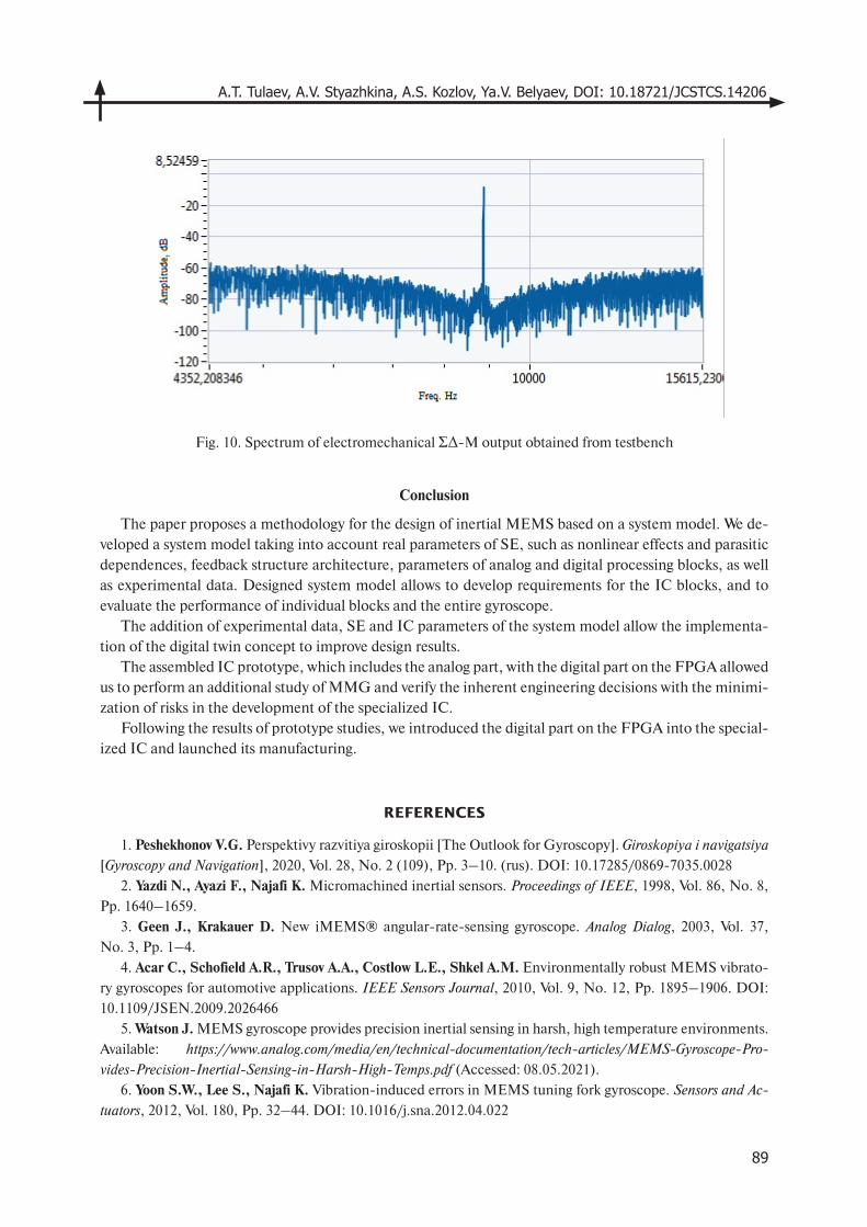
A.T. Tulaev, A.V. Styazhkina, A.S. Kozlov, Ya.V. Belyaev, DOI: 10.18721/JCSTCS.14206
89
Fig. 10. Spectrum of electromechanical ΣΔ-M output obtained from testbench
Conclusion
The paper proposes a methodology for the design of inertial MEMS based on a system model. We de-veloped a system model taking into account real parameters of SE, such as nonlinear effects and parasitic dependences, feedback structure architecture, parameters of analog and digital processing blocks, as well as experimental data. Designed system model allows to develop requirements for the IC blocks, and to evaluate the performance of individual blocks and the entire gyroscope.
The addition of experimental data, SE and IC parameters of the system model allow the implementa-tion of the digital twin concept to improve design results.
The assembled IC prototype, which includes the analog part, with the digital part on the FPGA allowed us to perform an additional study of MMG and verify the inherent engineering decisions with the minimi-zation of risks in the development of the specialized IС.
Following the results of prototype studies, we introduced the digital part on the FPGA into the special-ized IC and launched its manufacturing.
REFERENCES
1. Peshekhonov V.G. Perspektivy razvitiya giroskopii [The Outlook for Gyroscopy]. Giroskopiya i navigatsiya
[Gyroscopy and Navigation], 2020, Vol. 28, No. 2 (109), Pp. 3–10. (rus). DOI: 10.17285/0869-7035.0028
2. Yazdi N., Ayazi F., Najafi K. Micromachined inertial sensors. Proceedings of IEEE, 1998, Vol. 86, No. 8,
Pp. 1640–1659.
3. Geen J., Krakauer D. New iMEMS® angular-rate-sensing gyroscope. Analog Dialog, 2003, Vol. 37,
No. 3, Pp. 1–4.
4. Acar C., Schofield A.R., Trusov A.A., Costlow L.E., Shkel A.M. Environmentally robust MEMS vibrato-
ry gyroscopes for automotive applications. IEEE Sensors Journal, 2010, Vol. 9, No. 12, Pp. 1895–1906. DOI:
10.1109/JSEN.2009.2026466
5. Watson J. MEMS gyroscope provides precision inertial sensing in harsh, high temperature environments.
Available: https://www.analog.com/media/en/technical-documentation/tech-articles/MEMS-Gyroscope-Pro-
vides-Precision-Inertial-Sensing-in-Harsh-High-Temps.pdf (Accessed: 08.05.2021).
6. Yoon S.W., Lee S., Najafi K. Vibration-induced errors in MEMS tuning fork gyroscope. Sensors and Ac-
tuators, 2012, Vol. 180, Pp. 32–44. DOI: 10.1016/j.sna.2012.04.022
Computing, Telecommunications and Control Vol. 14, No. 2, 2021
90
7. Chen F., Li X., Kraft M. Electromechanical sigma delta modulators force feedback interfaces for capac-
itive MEMS inertial sensors: A Review. IEEE Sensors Journal, 2016, Vol. 16, No. 17, Pp. 6476–6495. DOI:
10.1109/JSEN.2016.2582198
8. Chen D., et al. A straightforward approach for synthesizing electromechanical sigma-delta MEMS accel-
erometers. Sensors, 2020, Vol. 20, No. 1, P. 91.
9. Gad M., Elshennawy A., Ismail A. A design method for delta sigma force-feedback accelerometer interface
systems. 2020 18th IEEE International New Circuits and Systems Conference (NEWCAS), IEEE, 2020, Pp. 5–8.
10. Xiong X., Li Z., Han K. Comparative study of single quantization architecture and dual quantization
architecture electromechanical sigma-delta modulators for MEMS accelerometer. 2020 IEEE International
Symposium on Inertial Sensors and Systems (INERTIAL), IEEE, 2020, Pp. 1–4.
11. Chiang C.T. Design of a CMOS MEMS accelerometer used in IoT devices for seismic detection. IEEE
Journal on Emerging and Selected Topics in Circuits and Systems, 2018, Vol. 8, No. 3, Pp. 566–577.
12. Jun J., et al. An SC interface with programmable-gain embedded delta sigma ADC for monolith-
ic three-axis 3D stacked capacitive MEMS accelerometer. IEEE Sensors Journal, 2017, Vol. 17, No. 17,
Pp. 5558–5568.
13. Chen D., et al. A ΣΔ closed-loop interface for a MEMS accelerometer with digital built-in self-test func-
tion. Micromachines, 2018, Vol. 9, No. 9, P. 444.
14. Li X., Hu J., Liu X. A high-performance digital interface circuit for a high-Q micro-electromechanical
system accelerometer. Micromachines, 2018, Vol. 9, No. 12, P. 675.
15. Lima V., et al. Small-size MEMS accelerometer encapsulated in vacuum using sigma-delta modulation.
2020 IEEE International Symposium on Inertial Sensors and Systems (INERTIAL), IEEE, 2020, Pp. 1–4.
16. Bafandeh A., Yavari M. Digital calibration of amplifier finite DC gain and gain bandwidth in MASH ΣΔ modulators. IEEE Transactions on Circuits and Systems II: Express Briefs, 2015, Vol. 63, No. 4, Pp. 321–325.
17. Hussain A., Hanif M. Active-pasisve delta-sigma modulator ADC for MEMS accelecrometers. 2017
International Symposium on Recent Advances in Electrical Engineering (RAEE), IEEE, 2017, Pp. 1–5.
18. Lukin A.V., Popov I.A., Belyayev Ya.V., Styazhkina A.V. Nelineynaya dinamika mikromekhanicheskogo
giroskopa RR-tipa v usloviyakh vibratsionnykh vozdeystviy [Nonlinear dynamics of an RR-type micromechan-
ical gyroscope under vibration conditions]. Materialy XXII konferentsii molodykh uchenykh s mezhdunarodnym
uchastiyem: Navigatsiya i upravleniye dvizheniyem [Proceeding of the XXII Conference on Navigation and Motion
Control], St. Petersburg, 2020, Pp. 37–40. (rus)
19. Belyaev Ya.V., Belogurov A.A., Kostygov D.V., Lemko I.V., Mihteeva A.A., Yakimova A.V., Nevirkovets
N.N., Chernetskaya N.M. Design of a micromechanical accelerometer. 25th Saint Petersburg International Con-
ference on Integrated Navigation Systems, St. Petersburg, 2018.
20. Yakimova A.V., Belogurov A.A., Belyaev Y.V. Design of sensing element of micromachined capacitive
MEMS accelerometer. Proceeding of the XIX Conference on Navigation and Motion Control, St. Petersburg, 2017,
Pp. 92–97.
21. Smirnov I.S., Belyayev Ya.V., Nevirkovets N.N. Deterministic algorithm for designing an operational
amplifier for an accelerometer integrated circuit. Proceeding of the XXI Conference on Navigation and Motion
Control, St. Petersburg, 2019, Pp. 201–203. (rus)
Received 26.05.2021.
СПИСОК ЛИТЕРАТУРЫ
1. Пешехонов В.Г. Перспективы развития гироскопии // Гироскопия и навигация, 2020. Т. 28. 2
(109). С. 3–10. DOI: 10.17285/0869-7035.0028
2. Yazdi N., Ayazi F., Najafi K. Micromachined Inertial Sensors // Proc. of IEEE.-1998. Vol. 86. No. 8.
Pp. 1640–1659.
A.T. Tulaev, A.V. Styazhkina, A.S. Kozlov, Ya.V. Belyaev, DOI: 10.18721/JCSTCS.14206
91
3. Geen J., Krakauer D. New iMEMS® angular-rate-sensing gyroscope // Analog Dialog. 2003. Vol. 37.
No. 3. Pp. 1–4.
4. Acar C., Schofield A.R., Trusov A.A., Costlow L.E., Shkel A.M. Environmentally robust MEMS vibratory
gyroscopes for automotive applications // IEEE Sensors Journal. 2010. Vol. 9. No. 12. Pp. 1895–1906. DOI:
10.1109/JSEN.2009.2026466
5. Watson J. MEMS gyroscope provides precision inertial sensing in harsh, high temperature environ-
ments // URL: https://www.analog.com/media/en/technical-documentation/tech-articles/MEMS-Gyro-
scope-Provides-Precision-Inertial-Sensing-in-Harsh-High-Temps.pdf (Дата обращения: 08.05.2021).
6. Yoon S.W., Lee S., Najafi K. Vibration-induced errors in MEMS tuning fork gyroscope // Sensors and
Actuators. 2012. Vol. 180. Pp. 32–44. DOI: 10.1016/j.sna.2012.04.022
7. Chen F., Li X., Kraft M. Electromechanical sigma delta modulators force feedback interfaces for capac-
itive MEMS inertial sensors: A Review // IEEE Sensors Journal. 2016. Vol. 16. No. 17. Pp. 6476–6495. DOI:
10.1109/JSEN.2016.2582198
8. Chen D., et al. A straightforward approach for synthesizing electromechanical sigma-delta MEMS accel-
erometers // Sensors. 2020. Vol. 20. No. 1. P. 91.
9. Gad M., Elshennawy A., Ismail A. A design method for delta sigma force-feedback accelerometer inter-
face systems // 2020 18th IEEE Internat. New Circuits and Systems Conf. IEEE, 2020. Pp. 5–8.
10. Xiong X., Li Z., Han K. Comparative study of single quantization architecture and dual quantization ar-
chitecture electromechanical sigma-delta modulators for MEMS accelerometer // 2020 IEEE Internat. Symp.
on Inertial Sensors and Systems. IEEE, 2020. Pp. 1–4.
11. Chiang C.T. Design of a CMOS MEMS accelerometer used in IoT devices for seismic detection // IEEE
Journal on Emerging and Selected Topics in Circuits and Systems. 2018. Vol. 8. No. 3. Pp. 566–577.
12. Jun J., et al. An SC interface with programmable-gain embedded delta sigma ADC for monolith-
ic three-axis 3D stacked capacitive MEMS accelerometer // IEEE Sensors Journal. 2017. Vol. 17. No. 17.
Pp. 5558–5568.
13. Chen D., et al. A ΣΔ closed-loop interface for a MEMS accelerometer with digital built-in self-test
function // Micromachines. 2018. Vol. 9. No. 9. P. 444.
14. Li X., Hu J., Liu X. A high-performance digital interface circuit for a high-Q micro-electromechanical
system accelerometer // Micromachines. 2018. Vol. 9. No. 12. P. 675.
15. Lima V., et al. Small-size MEMS accelerometer encapsulated in vacuum using sigma-delta modulation
// 2020 IEEE Internat. Symp. on Inertial Sensors and Systems. IEEE, 2020. Pp. 1–4.
16. Bafandeh A., Yavari M. Digital calibration of amplifier finite DC gain and gain bandwidth in MASH ΣΔ modulators // IEEE Transactions on Circuits and Systems II: Express Briefs. 2015. Vol. 63. No. 4. Pp. 321–325.
17. Hussain A., Hanif M. Active-pasisve delta-sigma modulator ADC for MEMS accelecrometers // 2017
Internat. Symp. on Recent Advances in Electrical Engineering. IEEE, 2017. Pp. 1–5.
18. Лукин А.В., Попов И.А., Беляев Я.В., Стяжкина А.В. Нелинейная динамика микромеханическо-
го гироскопа RR-типа в условиях вибрационных воздействий // Матер. XXII конф. молодых ученых с
международным участием: Навигация и управление движением. 2020. С. 37–40.
19. Belyaev Ya.V., Belogurov A.A., Kostygov D.V., Lemko I.V., Mihteeva A.A., Yakimova A.V., Nevirkovets
N.N., Chernetskaya N.M. Design of a micromechanical accelerometer // 25th Saint Petersburg Internat. Conf.
on Integrated Navigation Systems. St. Petersburg, 2018.
20. Yakimova A.V., Belogurov A.A., Belyaev Y.V. Design of sensing element of micromachined capacitive
MEMS accelerometer // Proc. of the XIX Conf. on Navigation and Motion Control, St. Petersburg, 2017.
Pp. 92–97.
21. Смирнов И.С., Беляев Я.В., Невирковец Н.Н. Детерминированный алгоритм проектирования
операционного усилителя для интегральной схемы акселерометра // Матер. XXI конф. молодых уче-
ных с международным участием: Навигация и управление движением. 2019. С. 201–203.
Computing, Telecommunications and Control Vol. 14, No. 2, 2021
92
Статья поступила в редакцию 26.05.2021.
THE AUTHORS / СВЕДЕНИЯ ОБ АВТОРАХ
Tulaev Artyom T.Тулаев Артём ТолибовичE-mail: [email protected]
Styazhkina Anna V.Стяжкина Анна ВасильевнаE-mail: [email protected]
Kozlov Alexey S.Козлов Алексей СергеевичE-mail: [email protected]
Belyaev Yakov V.Беляев Яков ВалерьевичE-mail: [email protected]
© Санкт-Петербургский политехнический университет Петра Великого, 2021
ИНФОРМАТИКА, ТЕЛЕКОММУНИКАЦИИ И УПРАВЛЕНИЕ
COMPUTING, TELECOMMUNICATIONS AND CONTROL
Том 14, 2, 2021
Учредитель — Федеральное государственное бюджетное образовательное учреждениевысшего профессионального образования «Санкт-Петербургский государственный
политехнический университет»
Журнал зарегистрирован Федеральной службой по надзорув сфере информационных технологий и массовых коммуникаций (Роскомнадзор).
Свидетельство о регистрации ЭЛ ФС77-77378 от 25.12.2019 г.
Редакция журнала
д-р техн. наук, профессор А.С. Коротков — главный редакторЕ.А. Калинина — литературный редактор, корректор
Г.А. Пышкина — ответственный секретарь, выпускающий редактор
Телефон редакции (812)552-62-16
E-mail: [email protected]
Компьютерная верстка А.А. Кононова
Перевод на английский язык Д.Ю. Алексеева
Лицензия ЛР 020593 от 07.08.97
Дата выхода 30.06.2021. Формат 60×84 1/8
Санкт-Петербургский политехнический университет Петра Великого
Адрес университета и редакции: 195251, Санкт-Петербург, ул. Политехническая, д. 29.


