Embed Size (px)
Citation preview
CY8CKIT-026 CAN and LIN Shield Kit Guide
Doc. No. 002-03798 Rev. *C
Cypress Semiconductor198 Champion Court
San Jose, CA 95134-1709www.cypress.com
Copyrights
CY8CKIT-026 CAN and LIN Shield Kit Guide, Doc. No. 002-03798 Rev. *C 2
Copyrights
© Cypress Semiconductor Corporation, 2015-2017. This document is the property of Cypress Semiconductor Corporationand its subsidiaries, including Spansion LLC ("Cypress"). This document, including any software or firmware included or ref-erenced in this document ("Software"), is owned by Cypress under the intellectual property laws and treaties of the UnitedStates and other countries worldwide. Cypress reserves all rights under such laws and treaties and does not, except as spe-cifically stated in this paragraph, grant any license under its patents, copyrights, trademarks, or other intellectual propertyrights. If the Software is not accompanied by a license agreement and you do not otherwise have a written agreement withCypress governing the use of the Software, then Cypress hereby grants you a personal, non-exclusive, nontransferablelicense (without the right to sublicense) (1) under its copyright rights in the Software (a) for Software provided in source codeform, to modify and reproduce the Software solely for use with Cypress hardware products, only internally within your organi-zation, and (b) to distribute the Software in binary code form externally to end users (either directly or indirectly through resell-ers and distributors), solely for use on Cypress hardware product units, and (2) under those claims of Cypress's patents thatare infringed by the Software (as provided by Cypress, unmodified) to make, use, distribute, and import the Software solelyfor use with Cypress hardware products. Any other use, reproduction, modification, translation, or compilation of the Softwareis prohibited.
TO THE EXTENT PERMITTED BY APPLICABLE LAW, CYPRESS MAKES NO WARRANTY OF ANY KIND, EXPRESS ORIMPLIED, WITH REGARD TO THIS DOCUMENT OR ANY SOFTWARE OR ACCOMPANYING HARDWARE, INCLUDING,BUT NOT LIMITED TO, THE IMPLIED WARRANTIES OF MERCHANTABILITY AND FITNESS FOR A PARTICULAR PUR-POSE. To the extent permitted by applicable law, Cypress reserves the right to make changes to this document without fur-ther notice. Cypress does not assume any liability arising out of the application or use of any product or circuit described inthis document. Any information provided in this document, including any sample design information or programming code, isprovided only for reference purposes. It is the responsibility of the user of this document to properly design, program, and testthe functionality and safety of any application made of this information and any resulting product. Cypress products are notdesigned, intended, or authorized for use as critical components in systems designed or intended for the operation of weap-ons, weapons systems, nuclear installations, life-support devices or systems, other medical devices or systems (includingresuscitation equipment and surgical implants), pollution control or hazardous substances management, or other uses wherethe failure of the device or system could cause personal injury, death, or property damage ("Unintended Uses"). A criticalcomponent is any component of a device or system whose failure to perform can be reasonably expected to cause the failureof the device or system, or to affect its safety or effectiveness. Cypress is not liable, in whole or in part, and you shall andhereby do release Cypress from any claim, damage, or other liability arising from or related to all Unintended Uses of Cypressproducts. You shall indemnify and hold Cypress harmless from and against all claims, costs, damages, and other liabilities,including claims for personal injury or death, arising from or related to any Unintended Uses of Cypress products.
Cypress, the Cypress logo, Spansion, the Spansion logo, and combinations thereof, WICED, PSoC, CapSense, EZ-USB, F-RAM, and Traveo are trademarks or registered trademarks of Cypress in the United States and other countries. For a morecomplete list of Cypress trademarks, visit cypress.com. Other names and brands may be claimed as property of their respec-tive owners.
CY8CKIT-026 CAN and LIN Shield Kit Guide, Doc. No. 002-03798 Rev. *C 3
1. Introduction 6
1.1 Kit Contents .................................................................................................................61.2 Getting Started.............................................................................................................71.3 Additional Learning Resources....................................................................................91.4 Technical Support ......................................................................................................101.5 Acronyms...................................................................................................................101.6 Document Conventions .............................................................................................10
2. Installation 112.1 Before You Begin.......................................................................................................112.2 Install Software ..........................................................................................................122.3 Uninstall Software......................................................................................................142.4 Install Hardware.........................................................................................................14
3. Hardware 153.1 System Block Diagram ..............................................................................................153.2 CAN Physical Layer Transceiver Circuits ..................................................................173.3 LIN Physical Layer Transceiver Circuits ....................................................................203.4 Status LEDs...............................................................................................................223.5 Port Options with CY8CKIT-042/044 Pioneer Kit ......................................................233.6 Power Supply Configurations ....................................................................................24
4. Kit Operation 30
4.1 Default Jumper Settings on CY8CKIT-026 ................................................................304.2 CAN Communication Hardware Setup ......................................................................304.3 Using CAN Bus Analyzer Tool...................................................................................324.4 LIN Communication Hardware Setup ........................................................................344.5 Using LIN Bus Analyzer Tool.....................................................................................35
5. Example Projects 37
5.1 Using the Kit Example Projects .................................................................................375.2 CAN_Simplex_Tx_CY8CKIT-044 ..............................................................................385.3 CAN_Simplex_Rx_CY8CKIT-044..............................................................................415.4 LIN_Slave_CY8CKIT-042..........................................................................................455.5 LIN_Slave_CY8CKIT-044..........................................................................................495.6 Multiple_LIN_Slave_CY8CKIT-042 ...........................................................................49
Appendix 54Schematics 54Gerber Files 58Bill of Materials 62
Contents

CY8CKIT-026 CAN and LIN Shield Kit Guide, Doc. No. 002-03798 Rev. *C 4
Safety Information
Regulatory Compliance
The CY8CKIT-026 CAN and LIN Shield Kit is intended for use as a development platform forhardware or software in a laboratory environment. The board is an open system design, which doesnot include a shielded enclosure. This may cause interference to other electrical or electronicdevices in close proximity. In a domestic environment, this product may cause radio interference. Insuch cases, you may be required to take adequate preventive measures. In addition, this boardshould not be used near any medical equipment or RF devices.
Attaching additional wiring to this product or modifying the product operation from the factory defaultmay affect its performance and cause interference with other apparatus in the immediate vicinity. Ifsuch interference is detected, suitable mitigating measures should be taken.
The CAN and LIN Shield Kit, as shipped from the factory, has been verified to meet with therequirements of CE as a Class A product.
The CAN and LIN Shield Kit contains ESD-sensitivedevices. Electrostatic charges readily accumulate on thehuman body and any equipment, and can discharge withoutdetection. Permanent damage may occur on devicessubjected to high-energy discharges. Proper ESDprecautions are recommended to avoid performancedegradation or loss of functionality. Store unused kit boardsin the protective shipping package.
End-of-Life/Product Recycling
This kit has an end-of life five years from the date ofmanufacture mentioned on the back of the box. Contact yournearest recycler for discarding the kit.
CY8CKIT-026 CAN and LIN Shield Kit Guide, Doc. No. 002-03798 Rev. *C 5
General Safety Instructions
ESD Protection
ESD can damage boards and associated components. Cypress recommends that you performprocedures only at an ESD workstation. If such a workstation is not available, use appropriate ESDprotection by wearing an antistatic wrist strap attached to the chassis ground (any unpainted metalsurface) on your board when handling parts.
Handling Boards
CAN and LIN Shield Kit boards are sensitive to ESD. Hold the board only by its edges. Afterremoving the board from its box, place it on a grounded, static-free surface. Use a conductive foampad if available. Do not slide the board over any surface.

CY8CKIT-026 CAN and LIN Shield Kit Guide, Doc. No. 002-03798 Rev. *C 6
1. Introduction
Thank you for your interest in the CY8CKIT-026 CAN and LIN Shield Kit. This kit is intended to
demonstrate the CAN and LIN bus communications in Cypress’s PSoC® products.
The CY8CKIT-026 CAN and LIN Shield Kit is an Arduino compatible shield board that is used withseveral Cypress kits such as the CY8CKIT-042 PSoC 4 Pioneer Kit/CY8CKIT-044 PSoC 4 M-Series
Pioneer Kit or FM4-176L-S6E2GM - ARM® Cortex®-M4 MCU Pioneer Kit. It enables you to evaluatethe Controller Area Network (CAN) and Local Interconnect Network (LIN) slave communicationcapability of Cypress devices. You can design your own projects with easy-to-use CAN and LINslave components in Cypress’s PSoC Creator™ software, or by altering code examples providedwith this kit.
This kit guide provides details on the kit contents, hardware, example projects, schematics, andBOM.
1.1 Kit Contents
The CY8CKIT-026 CAN and LIN Shield Kit contains the following, as shown in Figure 1-1:
■ CAN and LIN Shield Board
■ Three jumper wires (5 inches each)
■ Three jumper wires (4 inches each)
■ Four connectors (one 10 × 1, two 8 × 1 and one 6 × 1)
■ Quick Start Guide
Figure 1-1. CY8CKIT-026 CAN and LIN Shield Kit

CY8CKIT-026 CAN and LIN Shield Kit Guide, Doc. No. 002-03798 Rev. *C 7
Introduction
Inspect the contents of the kit; if anything is missing, contact your nearest Cypress sales office forassistance. Go to www.cypress.com/support for more information on Cypress sales offices andsupport.
1.1.1 Kit Compatibility
This kit contains an Arduino compatible shield board and requires other Cypress kits (Arduniocompatible) to use it. It is designed to add CAN and LIN capabilities to the PSoC 4 Series PioneerKits (CY8CKIT-042/44) and FM4 kits such as FM4-176L-S6E2GM - ARM Cortex-M4 MCU PioneerKit.
This kit is also compatible with any other general Arduino compatible Kit which supports CAN/LINprotocol.
CAN and LIN are communication protocols and require more than one CAN or LIN node to set upcommunication between nodes. Therefore, it is recommended to have two CY8CKIT-044 PioneerKits or other compatible kits and two CY8CKIT-026 CAN and LIN Shield Kits. This enables you to setup CAN communication between two CAN nodes. An alternative recommendation is to have a CANor LIN bus emulator or analyzer. This enables you to emulate a CAN or LIN node to communicatewith the PSoC CAN or LIN controller. See sections Using CAN Bus Analyzer Tool on page 32 andUsing LIN Bus Analyzer Tool on page 35 for more details on using a CAN analyzer or LIN analyzertool with this kit.
For detailed information about the differences between PSoC 4 devices, go to www.cypress.com/psoc. For more information about Cypress kits, go to the Cypress Store atwww.cypress.com/shop.
1.2 Getting Started
This guide will help you to get acquainted with the CY8CKIT-026 CAN and LIN Shield Kit:
■ The Installation chapter on page 11 describes the installation of the kit software. This includes the PSoC Creator IDE to develop and debug the applications, and PSoC Programmer to program the .hex files on to the device.
■ The Hardware chapter on page 15 details the hardware content of the kit and the hardware operation.
■ The Kit Operation chapter on page 30 explains you on how to set-up the hardware connections in order to establish CAN and LIN communication using CY8CKIT-026.
■ The Example Projects chapter on page 37 describes code examples that will help you understand how to create your own CAN and LIN communication projects on PSoC 4.
■ The Appendix chapter on page 54 provides schematics, layout and the bill of materials (BOM).
Refer to the kit web page for the latest information on using this kit with various Cypress devices.The web page will be updated as new devices and development kits compatible with this shield arereleased to the market.
CY8CKIT-026 CAN and LIN Shield Kit Guide, Doc. No. 002-03798 Rev. *C 8
Introduction
1.2.1 Beginner Resources
An overview of PSoC devices is available at www.cypress.com/psoc. The web page includes a list ofPSoC device families, integrated design environments (IDEs), and associated development kits. Inaddition, refer to the following documents to get started with PSoC 4 devices and CAN/LINcommunication:
■ AN79953 - Getting Started with PSoC® 4.
■ CE97311 - PSoC® 4 M: CAN Simplex Communication with CapSense®.
■ CE96999 - Basic LIN Slave Implementation in PSoC® 4.
■ PSoC Creator 101 Training Series.
■ CE211027 - CAN Communication between FM4-S6E2Gx Series and PSoC® 4 M-Series using the CY8CKIT-026 CAN and LIN Shield Kit.
1.2.2 Hardware Requirements
CY8CKIT-026 plugs into any Arduino™ hardware-compatible development platforms from Cypress.This Kit provides example projects targeting the CY8CKIT-042 PSoC 4 Pioneer Kit and CY8CKIT-044 PSoC 4 M-Series Pioneer Kit. For FM4 Kit CAN example project and hardwareconnections, please refer to the Code Example CE211027 - CAN Communication between FM4-S6E2Gx Series and PSoC® 4 M-Series using the CY8CKIT-026 CAN and LIN Shield Kit.
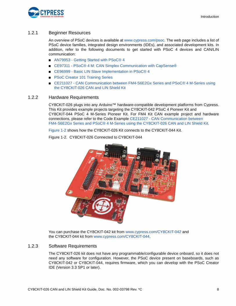
Figure 1-2 shows how the CY8CKIT-026 Kit connects to the CY8CKIT-044 Kit.
Figure 1-2. CY8CKIT-026 Connected to CY8CKIT-044
You can purchase the CY8CKIT-042 kit from www.cypress.com/CY8CKIT-042 and the CY8CKIT-044 kit from www.cypress.com/CY8CKIT-044.
1.2.3 Software Requirements
The CY8CKIT-026 kit does not have any programmable/configurable device onboard, so it does notneed any software for configuration. However, the PSoC device present on baseboards, such asCY8CKIT-042 or CY8CKIT-044, requires firmware, which you can develop with the PSoC CreatorIDE (Version 3.3 SP1 or later).
CY8CKIT-026 CAN and LIN Shield Kit Guide, Doc. No. 002-03798 Rev. *C 9
Introduction
1.2.3.1 PSoC Creator
PSoC Creator allows concurrent hardware and application firmware design of PSoC 3, PSoC 4, andPSoC 5LP systems. PSoC systems are designed using classic, familiar, schematic-capturetechnology supported by pre-verified, production ready PSoC Components™.
PSoC Components are analog and digital virtual chips represented by icons that you can drag anddrop into a design and configure to suit a broad array of application requirements. You can configureeach Component in the rich, mixed-signal Cypress Component Catalog with the ComponentCustomizer tool. These Components include a full set of dynamically generated API libraries. Afteryou have configured the PSoC system, you can write, compile, and debug the firmware within PSoCCreator, or export the firmware to other IDEs such as those from IAR, Keil, and Eclipse.
You can download the latest version of the PSoC Creator software from www.cypress.com/psoccreator. Refer to the Release Notes for the minimum and recommended system requirements.
1.2.3.2 PSoC Programmer
The PSoC Programmer software is used to program the PSoC 4 devices on the CY8CKIT-042 kitand CY8CKIT-044 kit with hex files. PSoC Programmer is installed along with PSoC Creator. Youcan also download PSoC Programmer separately at www.cypress.com/psocprogrammer.
1.3 Additional Learning Resources
Visit www.cypress.com for additional learning resources in the form of datasheets, technicalreference manuals, and application notes.
Code Example CE97311 describes the implementation of CAN bus communication between twoPSoC 4 devices. It explains how to send and receive CAN messages. It has two example projectswhich describe how to transmit/receive CAN messages using the CAN and LIN Shield Kit andCY8CKIT-044 PSoC 4 M-Series Pioneer Kit.
Code Example CE96999 describes the implementation of LIN bus communication using PSoC. Itexplains how to send and receive LIN messages. It has two example projects which describe how totransmit/receive LIN messages using the CAN and LIN Shield Kit and CY8CKIT-042/CY8CKIT-044PSoC 4 Pioneer Kits.
Code Example CE211027 describes the implementation of CAN bus communication between FM4-S6E2Gx Series and PSoC 4 M-Series. FM4 acts as Transmitter and PSoC 4 M acts as areceiver which changes the RGB LED color based on the commands received from the FM4.
CY8CKIT-026 CAN and LIN Shield Kit Guide, Doc. No. 002-03798 Rev. *C 10
Introduction
1.4 Technical Support
For assistance, go to our support web page (www.cypress.com/support) or contact our customersupport at +1(800) 541-4736 Ext. 2 (in the USA), or +1 (408) 943-2600 Ext. 2 (International).
1.5 Acronyms
1.6 Document Conventions
Table 1-1. Acronyms
Acronym Definition
BOM Bill of Materials
CAN Controlled Area Network
DLC Data Length Code
IDE Integrated Design Environment
LIN Local Interconnect Network
USB Universal Serial Bus
Table 1-2. Document Convention for Guides
Acronym Definition
Courier NewDisplays file locations, user entered text, and source code:
C:\...cd\icc\
ItalicsDisplays file names and reference documentation:
Read about the sourcefile.hex file in the PSoC Creator User Guide
[Bracketed, Bold]Displays keyboard commands in procedures:
[Enter] or [Ctrl] [C]
File > OpenRepresents menu paths:
File > Open > New Project
BoldDisplays commands, menu paths, and icon names in procedures: Click the File icon and then click Open.
Times New RomanDisplays an equation:
2 + 2 = 4
Text in gray boxes Describe s Cautions or unique functionality of the product.
CY8CKIT-026 CAN and LIN Shield Kit Guide, Doc. No. 002-03798 Rev. *C 11
2. Installation
This chapter describes the steps to install the software tools and packages on a computer for usingthe CAN and LIN Shield Kit along with PSoC Pioneer Kits. This includes the IDE on which the projects will be built and used for programming.
2.1 Before You Begin
All Cypress software installations require administrator privileges, but these are not required to runthe software after it is installed. Close any other Cypress software that is currently running beforeinstalling the kit software.
Note: By default, the kit contents are installed in C:\Program Files\Cypress\CY8CKIT-026CAN and LIN SHIELD KIT\<version> for a 32-bit machine and C:\Program Files(x86)\Cypress\CY8CKIT-026 CAN and LIN SHIELD KIT\<version> for a 64-bit machine.This folder will contain the kit example projects. To open the examples, it is recommended to use theprocedure described in the Code Example documents. That procedure will create an editable copyof the example in a path that you chose so that the original installed example will not be modified.
If you use a PSoC baseboard such as the CY8CKIT-042 or CY8CKIT-044 with the CY8CKIT-026CAN and LIN Shield Kit, you will require the PSoC Creator and PSoC Programmer softwareprograms to be installed before the kit can be used. If you run the CY8CKIT-026 installer file(CY8CKIT026Setup.exe), this will install PSoC Creator and Programmer. Otherwise, you caninstall these programs by downloading them from the following locations:
■ PSoC Programmer.
■ PSoC Creator.
CY8CKIT-026 CAN and LIN Shield Kit Guide, Doc. No. 002-03798 Rev. *C 12
Installation
2.2 Install Software
2.2.1 Installation from Internet
Perform these steps to install the CY8CKIT-026 CAN and LIN Shield Kit software from the internet(this is done to ensure the latest software is installed):
1. Go to kit web page.
2. Download and run the installer executable file (CY8CKIT026Setup.exe).
3. Run the installer executable file after it is downloaded.
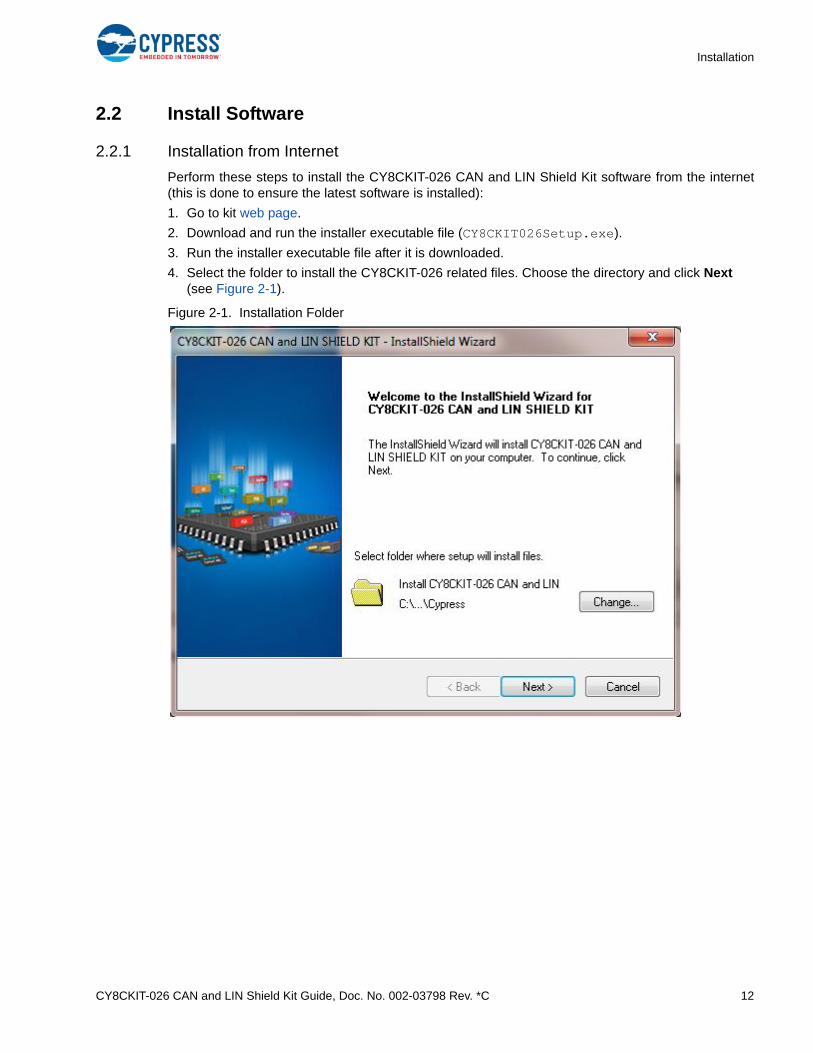
4. Select the folder to install the CY8CKIT-026 related files. Choose the directory and click Next (see Figure 2-1).
Figure 2-1. Installation Folder
CY8CKIT-026 CAN and LIN Shield Kit Guide, Doc. No. 002-03798 Rev. *C 13
Installation
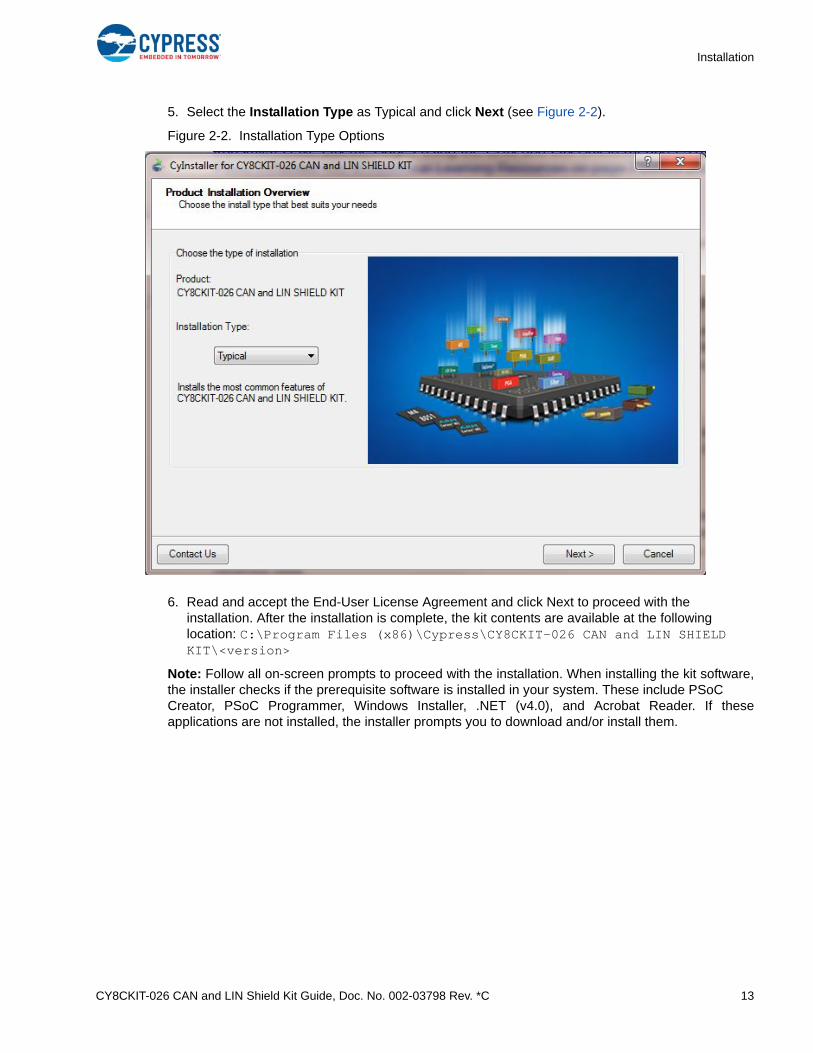
5. Select the Installation Type as Typical and click Next (see Figure 2-2).
Figure 2-2. Installation Type Options
6. Read and accept the End-User License Agreement and click Next to proceed with theinstallation. After the installation is complete, the kit contents are available at the following location: C:\Program Files (x86)\Cypress\CY8CKIT-026 CAN and LIN SHIELD KIT\<version>
Note: Follow all on-screen prompts to proceed with the installation. When installing the kit software,the installer checks if the prerequisite software is installed in your system. These include PSoC Creator, PSoC Programmer, Windows Installer, .NET (v4.0), and Acrobat Reader. If theseapplications are not installed, the installer prompts you to download and/or install them.

CY8CKIT-026 CAN and LIN Shield Kit Guide, Doc. No. 002-03798 Rev. *C 14
Installation
2.3 Uninstall Software
Perform these steps to uninstall the CY8CKIT-026 CAN and LIN Shield Kit software:
1. Go to Start > All Programs > Cypress > Cypress Update Manager and select the Uninstall button that corresponds to the kit software. Follow the on-screen prompts to uninstall the soft-ware. This is a program that is installed along with other Cypress software.
2. Go to Start > Control Panel > Programs and Features for Windows 7 or Add/Remove Programs for Windows XP; select the Uninstall/Change button.
2.4 Install Hardware
Perform these steps to install the hardware:
1. The Shield board must be physically attached to the Arduino header of the CY8CKIT-042/044 Pioneer Kit.
Note: This kit guide explains how to use this Shield Kit with Arduino headers of the CY8CKIT-044/042 Pioneer Kit. You can also attach this board to any Arduino based kit (controller must support CAN/LIN protocol). Modify pin assignments of the example projects to use with other kits. See Port Options with CY8CKIT-042/044 Pioneer Kit on page 23 for pin assignment details and limitations of using with CY8CKIT-044/042 Pioneer Kit Arduino ports.
2. Connect a USB Mini cable to your computer, to program this kit’s code examples into the PSoC device. Follow the instructions in the QSG (Quick Start Guide) documentation of the corresponding kit to connect it to your computer.
3. For the CAN example evaluation, perform these steps:
a. Connect two CAN and LIN shield boards together with a male-to-male, 9-pin, RS-232 cable with “straight-through” connections, as shown in Figure 4-1 on page 31, or
b. Connect a CAN analyzer to DB9 female connector of the Shield Kit.
For the LIN example evaluation, connect VCC, LIN bus, and GND of the LIN analyzer to connector J5 or J14 of the Shield Kit.
CY8CKIT-026 CAN and LIN Shield Kit Guide, Doc. No. 002-03798 Rev. *C 15
3. Hardware
3.1 System Block Diagram
The actual kit hardware files i.e., Schematic, Gerber, BOM etc are available in the installer directoryi.e., <Install_Directory>\CY8CKIT-026 CAN and LIN SHIELD KIT\<version>\Hardware
The CAN and LIN Shield Kit hardware consists of the following functional blocks:
■ 2-CAN transceiver circuits (TJA1051T and TJA1055T)
■ 2-LIN transceiver circuits in slave configuration (TJA1020)
■ Three status indicator LEDs
■ Arduino header
■ 12 V input Power Jack and Screw terminals for the same
■ Power circuitry for 12 V to 5 V dc conversion
■ PMIC for 12 V to 5 V dc conversion (not populated)
The primary functional blocks of this Shield Kit are the four transceiver circuits: two CAN transceivercircuits and two LIN transceiver circuits. Each of these transceiver circuits enables a digital CMOSPSoC device to interface with a physical CAN or LIN bus, respectively. Without these transceiver circuits, it is impossible for CMOS devices to communicate with other CAN or LIN nodes on a CANor LIN bus.
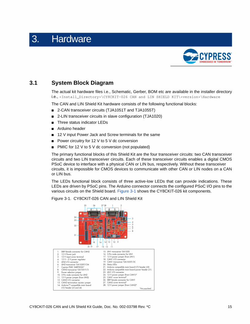
The LEDs functional block consists of three active-low LEDs that can provide indications. TheseLEDs are driven by PSoC pins. The Arduino connector connects the configured PSoC I/O pins to thevarious circuits on the Shield board. Figure 3-1 shows the CY8CKIT-026 kit components.
Figure 3-1. CY8CKIT-026 CAN and LIN Shield Kit
1. DB9 female connector for CAN22. 12 V Power jack3. 12 V input screw terminal4. 12 V – 5 V power regulator5. LIN2 I/O connector6. LIN2 transceiver TJA1020T/CM7. Cypress PMIC S6BP202A*8. CAN2 transceiver TJA1051T/39. Power selection jumper10. 3-Pin male connector for LIN211. 12 V power jumper (from LIN2)12. CAN2 I/O connector13. CAN2 termination resistor jumper14. Arduino™ compatible main board I/O header (J3 and J4)
15. LIN1 transceiver TJA102016. 3-Pin male connector for LIN117. 12 V power jumper (from LIN1)18. CAN1 I/O connector19. CAN1 transceiver TJA1055T/3C20. Status LEDs21. Arduino compatible main board I/O header (J2)22. Arduino compatible main board power header (J1) 23. LIN1 I/O connector24. 12 V power jumper (from CAN1)* 25. CAN1 screw terminal*26. DB9 female connector for CAN127. CAN2 screw terminal*28. 12 V power jumper (from CAN2)*
1 2
3
45678
910
11
1214
1315
16
17
18
1920
21
22
23
24
25 26 27 28
*Not populated
CY8CKIT-026 CAN and LIN Shield Kit Guide, Doc. No. 002-03798 Rev. *C 16
Hardware
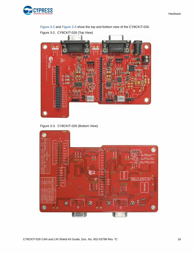
Figure 3-2 and Figure 3-3 show the top and bottom view of the CY8CKIT-026.
Figure 3-2. CY8CKIT-026 (Top View)
Figure 3-3. CY8CKIT-026 (Bottom View)
CY8CKIT-026 CAN and LIN Shield Kit Guide, Doc. No. 002-03798 Rev. *C 17
Hardware
3.2 CAN Physical Layer Transceiver Circuits
The CY8CKIT-026 has two CAN transceivers: one is low speed (up to 125 Kbps baud rate) and faulttolerant, and the other is high speed (up to 2 Mbps baud rate). The PSoC 4M device supports twoCAN modules, so these two transceivers enable you to use both of them to connect to CAN net-works.
The CAN physical layer transceiver circuits (CAN1 Transceiver and CAN2 Transceiver) on the shieldboard use TJA1055T and TJA1051T CAN transceiver devices. These devices translate differentialCAN bus signals to and from digital CMOS signals.
■ CAN1 Transceiver (TJA1055T)
Three signals are used between this circuit and the CAN (PSoC 4) controller. These signals areCAN1_RX, CAN1_TX, and CAN1_ERR. Data signals on the CAN bus are driven to the PSoCCAN1_RX signal. Data signals on the PSoC CAN1_TX signal are driven onto the CAN bus. TheCAN1_ER signal is used to indicate an error event. See the TJA1055T device datasheet for detailson each of these three pins of the CAN transceiver.
■ CAN2 Transceiver (TJA1051T)
Three signals are used between this circuit and the CAN (PSoC 4) controller. These signals areCAN_RX, CAN_TX, and CAN_EN. Data signals on the CAN bus are driven to the PSoC CAN2_RXsignal. Data signals on the PSoC CAN2_TX signal are driven onto the CAN bus. The CAN_EN signal enables and disables the CAN transceiver. See the TJA1051T device datasheet for details oneach of these three pins of the CAN transceiver.
3.2.1 CAN Bus Clock Accuracy
For accurate CAN communication, a CAN controller device must typically have a clock source with afrequency tolerance of 0.5% or less for bit-rates faster than 125 Kbps and at least 1.58% for 125 Kbps or slower bit-rates. Therefore, the device used as the CAN controller must meet thisrequirement. Otherwise, an external clock source that is more accurate must be used. But, PSoC 4has a great feature where you can trim the internal IMO clock up to 0.5% accuracy. See CE97311code example for details on the clock configuration of this kit's code examples.
3.2.2 CAN Bus Connector
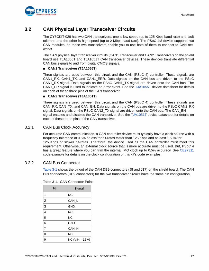
Table 3-1 shows the pinout of the CAN DB9 connectors (J8 and J17) on the shield board. The CANBus connectors (DB9 connectors) for the two transceiver circuits have the same pin configuration.
Table 3-1. CAN Connector Point
Pin Signal
1 NC
2 CAN_L
3 GND
4 NC
5 NC
6 GND
7 CAN_H
8 NC
9 NC (VIN = 12 V)

CY8CKIT-026 CAN and LIN Shield Kit Guide, Doc. No. 002-03798 Rev. *C 18
Hardware
By default, pin 9 of the CAN connector is left floating. However, if the jumper (J13 for CAN1transceiver and J21 for CAN2 transceiver) is populated, pin 9 of the CAN connector is connected tothe VIN power rail of the Shield board. This is useful if you want to power up other CAN nodesthrough the CAN connector or if you want to power up the Shield board from the power supply ofsome other CAN node.
3.2.3 CAN Bus Termination for CAN1 Transceiver
The CAN specification requires that CAN nodes located physically at the end of the CAN bus mustterminate the CAN differential signals with 120 . TJA1055 has CAN Bus termination pins as RTHand RTL which are connected to CAN_H and CAN_L with 120 respectively.
3.2.4 CAN Bus Termination for CAN2 Transceiver
The CAN specification requires that CAN nodes located physically at the end of the CAN bus mustterminate the CAN differential signals with 120. The Shield Kit features a 120- termination resis-tor (R17) that can be enabled or disabled by using jumper J10. If J10 is populated, the terminationresistor is active. If J10 is not populated, the termination resistor is not active.
By default, the termination resistor is active (J10 is populated).
Figure 3-4. J10 Jumper
Caution: Ensure extra care when populating jumpers J13 or J21. The shield Kit or Pioneer Kit can be damaged if the shield has it’s own power supply powering the VIN rail and a different power supply is connected through pin 9 of the CAN connectors.
CY8CKIT-026 CAN and LIN Shield Kit Guide, Doc. No. 002-03798 Rev. *C 19
Hardware
3.2.5 Choke Footprint
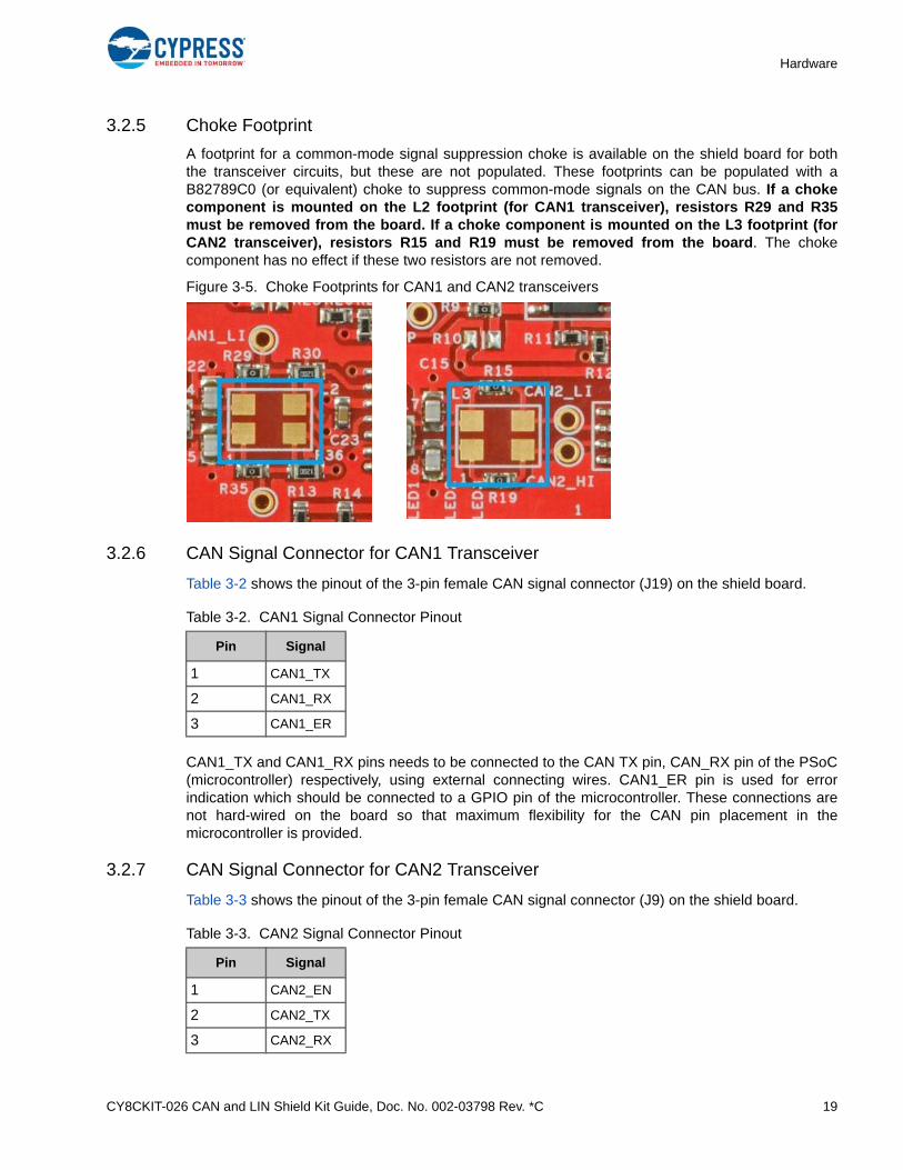
A footprint for a common-mode signal suppression choke is available on the shield board for boththe transceiver circuits, but these are not populated. These footprints can be populated with aB82789C0 (or equivalent) choke to suppress common-mode signals on the CAN bus. If a chokecomponent is mounted on the L2 footprint (for CAN1 transceiver), resistors R29 and R35must be removed from the board. If a choke component is mounted on the L3 footprint (forCAN2 transceiver), resistors R15 and R19 must be removed from the board. The chokecomponent has no effect if these two resistors are not removed.
Figure 3-5. Choke Footprints for CAN1 and CAN2 transceivers
3.2.6 CAN Signal Connector for CAN1 Transceiver
Table 3-2 shows the pinout of the 3-pin female CAN signal connector (J19) on the shield board.
CAN1_TX and CAN1_RX pins needs to be connected to the CAN TX pin, CAN_RX pin of the PSoC(microcontroller) respectively, using external connecting wires. CAN1_ER pin is used for errorindication which should be connected to a GPIO pin of the microcontroller. These connections arenot hard-wired on the board so that maximum flexibility for the CAN pin placement in themicrocontroller is provided.
3.2.7 CAN Signal Connector for CAN2 Transceiver
Table 3-3 shows the pinout of the 3-pin female CAN signal connector (J9) on the shield board.
Table 3-2. CAN1 Signal Connector Pinout
Pin Signal
1 CAN1_TX
2 CAN1_RX
3 CAN1_ER
Table 3-3. CAN2 Signal Connector Pinout
Pin Signal
1 CAN2_EN
2 CAN2_TX
3 CAN2_RX
CY8CKIT-026 CAN and LIN Shield Kit Guide, Doc. No. 002-03798 Rev. *C 20
Hardware
CAN2_TX and CAN2_RX pins need to be connected to the CAN TX pin, CAN_RX pin of the PSoC(microcontroller) respectively, using external connecting wires. CAN2_EN pin is used enable/disablethe transceiver which should be connected to the CAN_EN pin of the microcontroller. The trans-ceiver is enabled by default. These connections are not hard-wired on the board so that maximumflexibility for the CAN pin placement in the microcontroller is provided.
3.3 LIN Physical Layer Transceiver Circuits
The CY8CKIT-026 has two LIN transceivers. Since some PSoC 4 devices support two LIN slaves,these two transceivers enable you to use both of them simultaneously.
The two LIN physical layer transceiver circuits on the shield board use a TJA1020 LIN transceiver device. This device translates high-voltage LIN bus signals to and from digital CMOSsignals with standard TTL voltage levels.
Three signals are used between each LIN circuit and the LIN (PSoC 4) controller. For the LIN1 cir-cuit, the three signals are: LIN1_RX, LIN1_TX, and LIN1_NSLP. For the LIN2 circuit, the signals are:LIN2_RX, LIN2_TX, and LIN2_NSLP. Data signals on the LIN bus are sent to the PSoC by theLINx_RX signal. Data signals driven by the PSoC on the LINx_TX signal will be driven onto the LINbus. The LINx_NSLP signals are used to put the LIN transceiver device in and out of sleep.
By default, there are no pull-up resistors on the LINx_TX signals. A pull-up resistor footprint is pro-vided (R25 on LIN1_TX and R10 on LIN2_TX) on each LINx_TX signal if you want to have a pullupresistor on this signal. See the TJA1020 device datasheet for details on each of the three signals ofthe LIN transceiver.
3.3.1 LIN Bus Connectors
Figure 3-6 shows the pinout of both of the 3-pin LIN connectors (J14 for LIN1 transceiver and J5 forLIN2 transceiver) on the shield board.
Figure 3-6. LIN Connector Pinouts
By default, the jumpers J16 and J7 are populated. These connect pin 3 (VBAT1) of the LIN1connector and pin 3 (VBAT2) of the LIN2 connector to the VIN power rail of the Shield Kit,respectively. This is useful if you want to power up other LIN nodes/analyzers through either of theLIN connectors, or if you want to power the Pioneer Kit and shield board from the power supply(12 V) of some other LIN node (LIN analyzer).
CY8CKIT-026 CAN and LIN Shield Kit Guide, Doc. No. 002-03798 Rev. *C 21
Hardware
Ensure extra care when connecting an analyzer to either of the LIN connectors. If the LIN analyzerprovides 12 V supply already to its VBAT pin, remove jumper J16 for LIN1 connector and J7 for LIN2connector or do not power the shield with external 12 V supply through the J11 and J12 connectors.
3.3.2 Using the LIN Transceiver NWAKE Pins
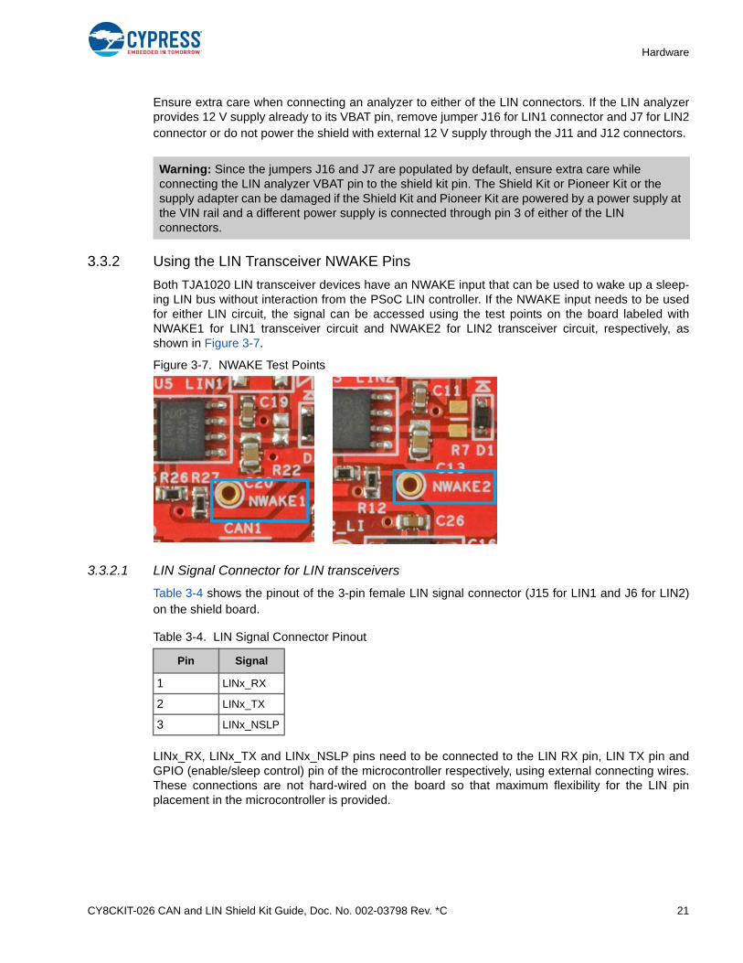
Both TJA1020 LIN transceiver devices have an NWAKE input that can be used to wake up a sleep-ing LIN bus without interaction from the PSoC LIN controller. If the NWAKE input needs to be usedfor either LIN circuit, the signal can be accessed using the test points on the board labeled withNWAKE1 for LIN1 transceiver circuit and NWAKE2 for LIN2 transceiver circuit, respectively, asshown in Figure 3-7.
Figure 3-7. NWAKE Test Points
3.3.2.1 LIN Signal Connector for LIN transceivers
Table 3-4 shows the pinout of the 3-pin female LIN signal connector (J15 for LIN1 and J6 for LIN2)on the shield board.
LINx_RX, LINx_TX and LINx_NSLP pins need to be connected to the LIN RX pin, LIN TX pin andGPIO (enable/sleep control) pin of the microcontroller respectively, using external connecting wires.These connections are not hard-wired on the board so that maximum flexibility for the LIN pinplacement in the microcontroller is provided.
Warning: Since the jumpers J16 and J7 are populated by default, ensure extra care while connecting the LIN analyzer VBAT pin to the shield kit pin. The Shield Kit or Pioneer Kit or the supply adapter can be damaged if the Shield Kit and Pioneer Kit are powered by a power supply at the VIN rail and a different power supply is connected through pin 3 of either of the LIN connectors.
Table 3-4. LIN Signal Connector Pinout
Pin Signal
1 LINx_RX
2 LINx_TX
3 LINx_NSLP
CY8CKIT-026 CAN and LIN Shield Kit Guide, Doc. No. 002-03798 Rev. *C 22
Hardware
3.3.3 LIN Master and Slave Configurations
By default, both the LIN circuits are configured for LIN slave operation. Table 3-5 shows how eachcircuit is populated by default to configure it for the LIN slave mode.
The components can be replaced as provided in Table 3-6 to change the circuit from a slave to amaster.
3.4 Status LEDs
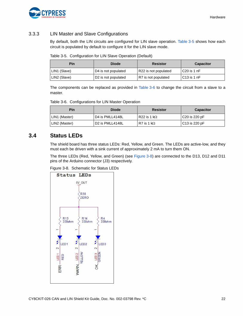
The shield board has three status LEDs: Red, Yellow, and Green. The LEDs are active-low, and theymust each be driven with a sink current of approximately 2 mA to turn them ON.
The three LEDs (Red, Yellow, and Green) (see Figure 3-8) are connected to the D13, D12 and D11pins of the Arduino connector (J3) respectively.
Figure 3-8. Schematic for Status LEDs
Table 3-5. Configuration for LIN Slave Operation (Default)
Pin Diode Resistor Capacitor
LIN1 (Slave) D4 is not populated R22 is not populated C20 is 1 nF
LIN2 (Slave) D2 is not populated R7 is not populated C13 is 1 nF
Table 3-6. Configurations for LIN Master Operation
Pin Diode Resistor Capacitor
LIN1 (Master) D4 is PMLL4148L R22 is 1 k C20 is 220 pF
LIN2 (Master) D2 is PMLL4148L R7 is 1 k C13 is 220 pF
CY8CKIT-026 CAN and LIN Shield Kit Guide, Doc. No. 002-03798 Rev. *C 23
Hardware
All three LEDs can be completely isolated from the rest of the Pioneer Kit by removing resistor R38,which is a 0 resistor. This is useful if the LEDs are not needed, but other circuits on the Shield Kitare needed. In this case, isolating the LEDs ensures that they do not interfere with other circuits thatshare the same pins.
3.5 Port Options with CY8CKIT-042/044 Pioneer Kit
The CAN and LIN Shield Kit connects to the CY8CKIT-042 or CY8CKIT-044 PSoC 4 series PioneerKits through the Arduino header connector. Table 3-7 shows how the signals on the CAN and LINshield board map to the pins on Arduino header of the CY8CKIT-042 and CY8CKIT-044 PioneerKits.
Table 3-7. Arduino Port Pin Connections
Arduino Connector Pin CY8CKIT-042 CY8CKIT-044 CY8CKIT-026
J1
1 VIN VIN VIN
2 GND GND GND
3 GND GND GND
4 V5.0 V5.0 V5.0
5 V3.3 V3.3 V3.3
6 Reset Reset Reset
7 P4.VDD P4.VDD P4.VDD
8 NC NC NC
J2
1 P2.0 P2.0 A0
2 P0.2 P2.6 J2_2
3 P2.1 P2.1 A1
4 P0.3 P6.5 J2_4
5 P2.2 P2.2 A2
6 P4.VDD P0.6 J2_6
7 P2.3 P2.3 A3
8 P1.5 P4.4 J2_8
9 P2.4 P2.4 A4
10 P1.4 P4.5 J2_10
11 P2.5 P2.5 A5
12 P1.3 P4.6 J2_12
13 P0.0 P0.0 J2_13
14 GND GND GND
15 P0.1 P0.1 J2_15
16 P1.2 P3.4 J2_16
17 P1.0 P0.7 J2_17
18 P1.1 P3.5 J2_18

CY8CKIT-026 CAN and LIN Shield Kit Guide, Doc. No. 002-03798 Rev. *C 24
Hardware
3.6 Power Supply Configurations
By default, the CAN and LIN shield board is powered from the Baseboard (CY8CKIT-042/044) byshorting pins 1 and 2 of the 4-pin (1x4) connector (J20). This supplies 5 V to the shield board. Notethat this will only allow CAN2 to be used since CAN1, LIN1 and LIN2 require a 12 V supply.
J3
1 P2.6 P0.2 D8
2 P3.6 P0.3 D9
3 P3.4 P2.7 D10
4 P3.0 P6.0 D11
5 P3.1 P6.1 D12
6 P0.6 P6.2 D13
7 GND GND GND
8 P1.7 (AREF) P1.7 (AREF) AREF
9 P4.1 (SDA) P4.1 (SDA) SDA
10 P4.0 (SCL) P4.0 (SCL) SCL
J4
1 P0.4 P3.0 D0
2 P0.5 P3.1 D1
3 P0.7 P1.0 D2
4 P3.7 P1.1 D3
5 P0.0 P1.2 D4
6 P3.5 P1.3 D5
7 P1.0 P5.3 D6
8 P2.7 P5.5 D7
Table 3-7. Arduino Port Pin Connections (continued)
Arduino Connector Pin CY8CKIT-042 CY8CKIT-044 CY8CKIT-026
CY8CKIT-026 CAN and LIN Shield Kit Guide, Doc. No. 002-03798 Rev. *C 25
Hardware
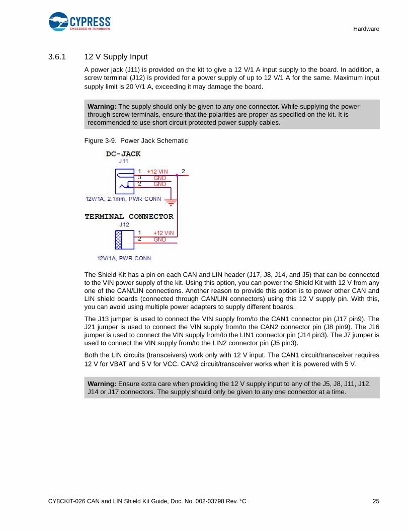
3.6.1 12 V Supply Input
A power jack (J11) is provided on the kit to give a 12 V/1 A input supply to the board. In addition, ascrew terminal (J12) is provided for a power supply of up to 12 V/1 A for the same. Maximum inputsupply limit is 20 V/1 A, exceeding it may damage the board.
Figure 3-9. Power Jack Schematic
The Shield Kit has a pin on each CAN and LIN header (J17, J8, J14, and J5) that can be connectedto the VIN power supply of the kit. Using this option, you can power the Shield Kit with 12 V from anyone of the CAN/LIN connections. Another reason to provide this option is to power other CAN andLIN shield boards (connected through CAN/LIN connectors) using this 12 V supply pin. With this,you can avoid using multiple power adapters to supply different boards.
The J13 jumper is used to connect the VIN supply from/to the CAN1 connector pin (J17 pin9). TheJ21 jumper is used to connect the VIN supply from/to the CAN2 connector pin (J8 pin9). The J16jumper is used to connect the VIN supply from/to the LIN1 connector pin (J14 pin3). The J7 jumper isused to connect the VIN supply from/to the LIN2 connector pin (J5 pin3).
Both the LIN circuits (transceivers) work only with 12 V input. The CAN1 circuit/transceiver requires12 V for VBAT and 5 V for VCC. CAN2 circuit/transceiver works when it is powered with 5 V.
Warning: The supply should only be given to any one connector. While supplying the power through screw terminals, ensure that the polarities are proper as specified on the kit. It is recommended to use short circuit protected power supply cables.
Warning: Ensure extra care when providing the 12 V supply input to any of the J5, J8, J11, J12, J14 or J17 connectors. The supply should only be given to any one connector at a time.
CY8CKIT-026 CAN and LIN Shield Kit Guide, Doc. No. 002-03798 Rev. *C 26
Hardware
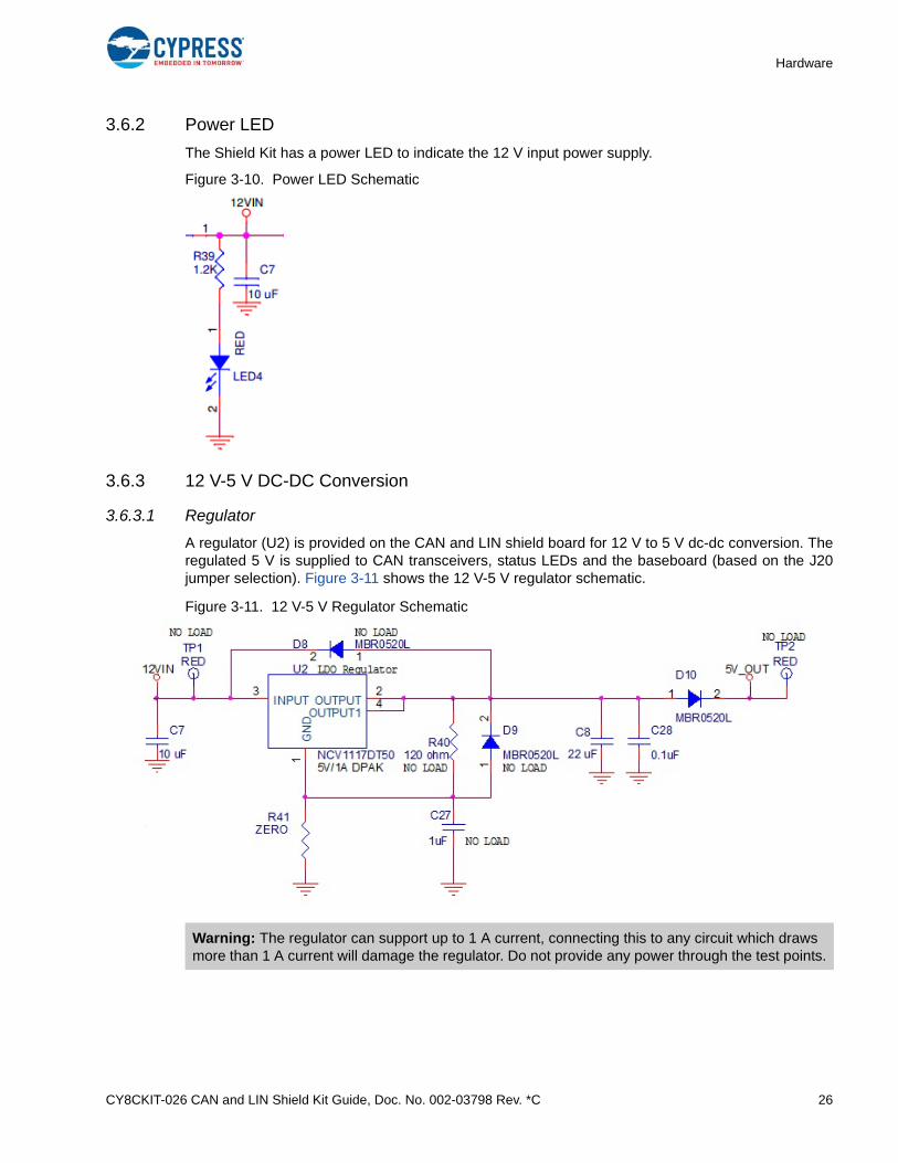
3.6.2 Power LED
The Shield Kit has a power LED to indicate the 12 V input power supply.
Figure 3-10. Power LED Schematic
3.6.3 12 V-5 V DC-DC Conversion
3.6.3.1 Regulator
A regulator (U2) is provided on the CAN and LIN shield board for 12 V to 5 V dc-dc conversion. Theregulated 5 V is supplied to CAN transceivers, status LEDs and the baseboard (based on the J20jumper selection). Figure 3-11 shows the 12 V-5 V regulator schematic.
Figure 3-11. 12 V-5 V Regulator Schematic
Warning: The regulator can support up to 1 A current, connecting this to any circuit which draws more than 1 A current will damage the regulator. Do not provide any power through the test points.
CY8CKIT-026 CAN and LIN Shield Kit Guide, Doc. No. 002-03798 Rev. *C 27
Hardware
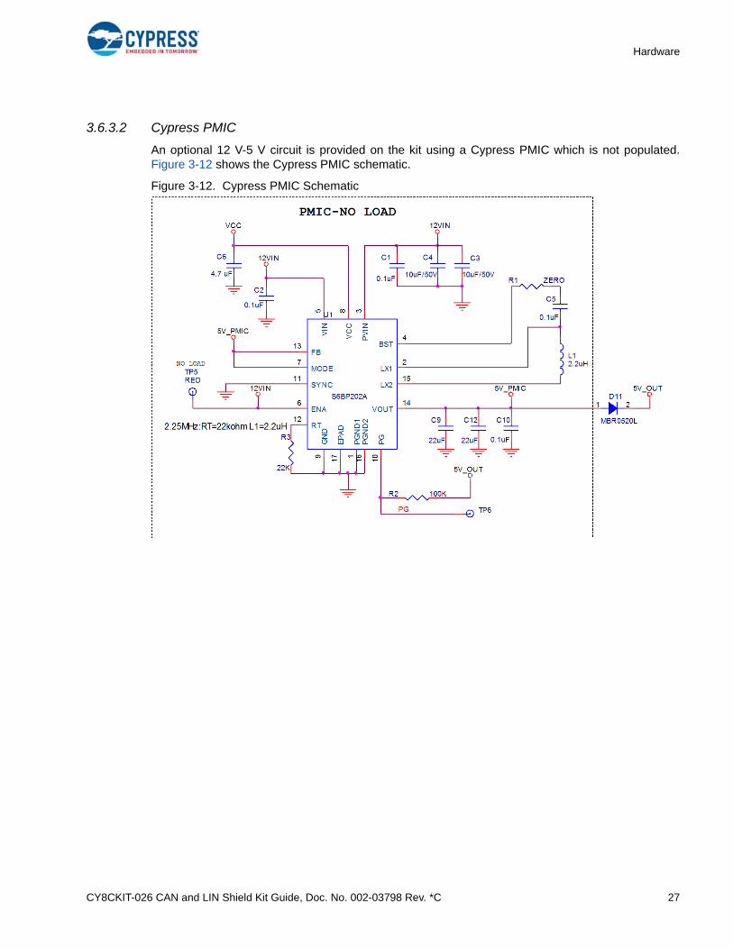
3.6.3.2 Cypress PMIC
An optional 12 V-5 V circuit is provided on the kit using a Cypress PMIC which is not populated.Figure 3-12 shows the Cypress PMIC schematic.
Figure 3-12. Cypress PMIC Schematic
CY8CKIT-026 CAN and LIN Shield Kit Guide, Doc. No. 002-03798 Rev. *C 28
Hardware
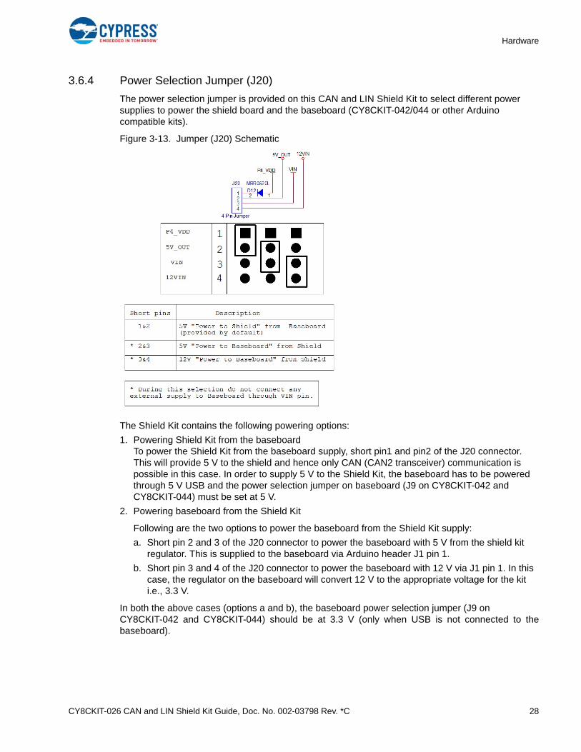
3.6.4 Power Selection Jumper (J20)
The power selection jumper is provided on this CAN and LIN Shield Kit to select different power supplies to power the shield board and the baseboard (CY8CKIT-042/044 or other Arduino compatible kits).
Figure 3-13. Jumper (J20) Schematic
The Shield Kit contains the following powering options:
1. Powering Shield Kit from the baseboardTo power the Shield Kit from the baseboard supply, short pin1 and pin2 of the J20 connector. This will provide 5 V to the shield and hence only CAN (CAN2 transceiver) communication is possible in this case. In order to supply 5 V to the Shield Kit, the baseboard has to be powered through 5 V USB and the power selection jumper on baseboard (J9 on CY8CKIT-042 and CY8CKIT-044) must be set at 5 V.
2. Powering baseboard from the Shield Kit
Following are the two options to power the baseboard from the Shield Kit supply:
a. Short pin 2 and 3 of the J20 connector to power the baseboard with 5 V from the shield kit regulator. This is supplied to the baseboard via Arduino header J1 pin 1.
b. Short pin 3 and 4 of the J20 connector to power the baseboard with 12 V via J1 pin 1. In this case, the regulator on the baseboard will convert 12 V to the appropriate voltage for the kit i.e., 3.3 V.
In both the above cases (options a and b), the baseboard power selection jumper (J9 on CY8CKIT-042 and CY8CKIT-044) should be at 3.3 V (only when USB is not connected to thebaseboard).
CY8CKIT-026 CAN and LIN Shield Kit Guide, Doc. No. 002-03798 Rev. *C 29
Hardware
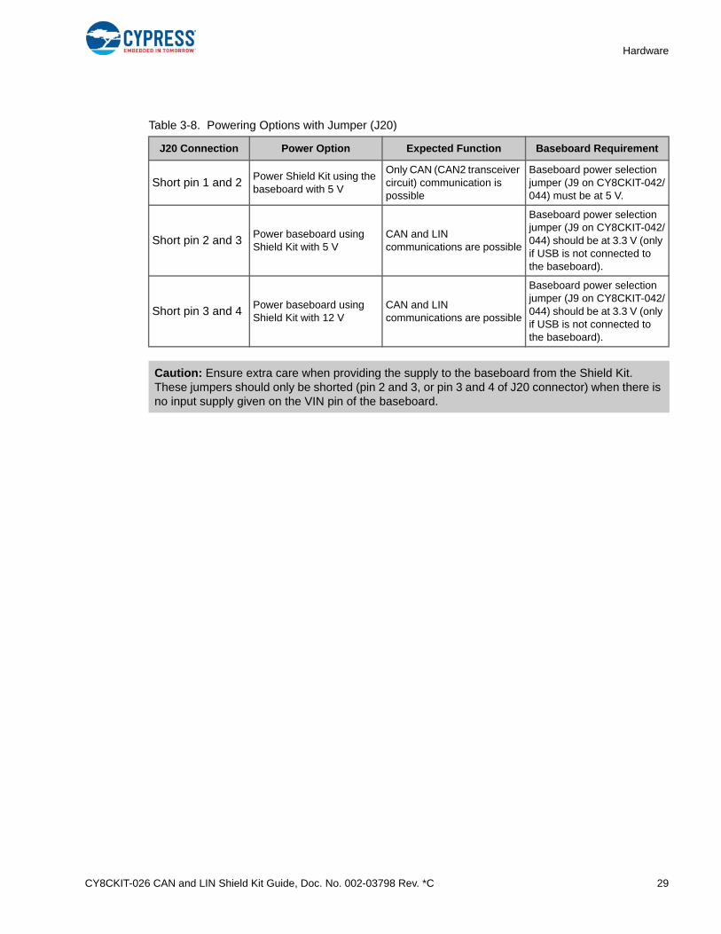
Table 3-8. Powering Options with Jumper (J20)
J20 Connection Power Option Expected Function Baseboard Requirement
Short pin 1 and 2Power Shield Kit using the baseboard with 5 V
Only CAN (CAN2 transceiver circuit) communication is possible
Baseboard power selection jumper (J9 on CY8CKIT-042/044) must be at 5 V.
Short pin 2 and 3Power baseboard using Shield Kit with 5 V
CAN and LIN communications are possible
Baseboard power selection jumper (J9 on CY8CKIT-042/044) should be at 3.3 V (only if USB is not connected to the baseboard).
Short pin 3 and 4Power baseboard using Shield Kit with 12 V
CAN and LIN communications are possible
Baseboard power selection jumper (J9 on CY8CKIT-042/044) should be at 3.3 V (only if USB is not connected to the baseboard).
Caution: Ensure extra care when providing the supply to the baseboard from the Shield Kit. These jumpers should only be shorted (pin 2 and 3, or pin 3 and 4 of J20 connector) when there is no input supply given on the VIN pin of the baseboard.
CY8CKIT-026 CAN and LIN Shield Kit Guide, Doc. No. 002-03798 Rev. *C 30
4. Kit Operation
This chapter explains how to set-up the hardware connections in order to establish CAN and LINcommunication using CY8CKIT-026.
4.1 Default Jumper Settings on CY8CKIT-026
Table 4-1 shows the default jumper settings of the CY8CKIT-026 CAN and LIN Shield Kit.
4.2 CAN Communication Hardware Setup1. Connect the CAN and LIN Shield Kit to the Arduino header of a CY8CKIT-044 Pioneer Kit, as
shown in Figure 1-2.
2. Connect a second CAN and LIN Shield Kit to the Arduino header of a second CY8CKIT-044 Pioneer Kit, as shown in Figure 1-2.
3. On both the CAN and LIN Shield Kits, connect the CAN TX and RX pins of the controller (Comes from the baseboard via the Arduino header) to CANx_TX and CANx_RX pins (on J19 connector for CAN1 transceiver, J9 connector of CAN2 transceiver) of the CAN transceiver circuit using connecting wires. See CAN Signal Connector for CAN1 Transceiver on page 19 and CAN Signal Connector for CAN2 Transceiver on page 19 for details of CAN TX and RX pin connections. See the Example Projects on page 37 for the specific pin connections used in the example projects.
Note: PSoC 4M supports two CAN modules. The supported CAN pins are:
a. P0[0] and P0[1] or P4[5] and P4[6] act as CAN_Rx and CAN_Tx for CAN1 module
b. P4[0] and P4[1] or P6[1] and P6[2] act as CAN_Rx and CAN_Tx for CAN2 module
4. Connect the two CAN and LIN Shield Kits together with a male-to-male, 9-pin, RS-232 cable with“straight-through” connections. Connect the DB9 cable to the corresponding CAN transceiver circuit DB9 connector (J17 for CAN1 transceiver and J8 for CAN2 transceiver) on both the shield kits.
Table 4-1. Default Settings of the CY8CKIT-026 CAN and LIN Shield Kit
Jumper Default Condition Function
J7 Populated Provides 12 V power from LIN2 connector
J10 Populated Enables CAN2 termination resistor
J13 Not populated Provides 12 V power from CAN1 connector
J16 Populated Provides 12 V power from LIN1 connector
J20 Populated between pin 1 and 2 Provides Power selection options
J21 Not populated Provides 12 V power from CAN2 connector
CY8CKIT-026 CAN and LIN Shield Kit Guide, Doc. No. 002-03798 Rev. *C 31
Kit Operation
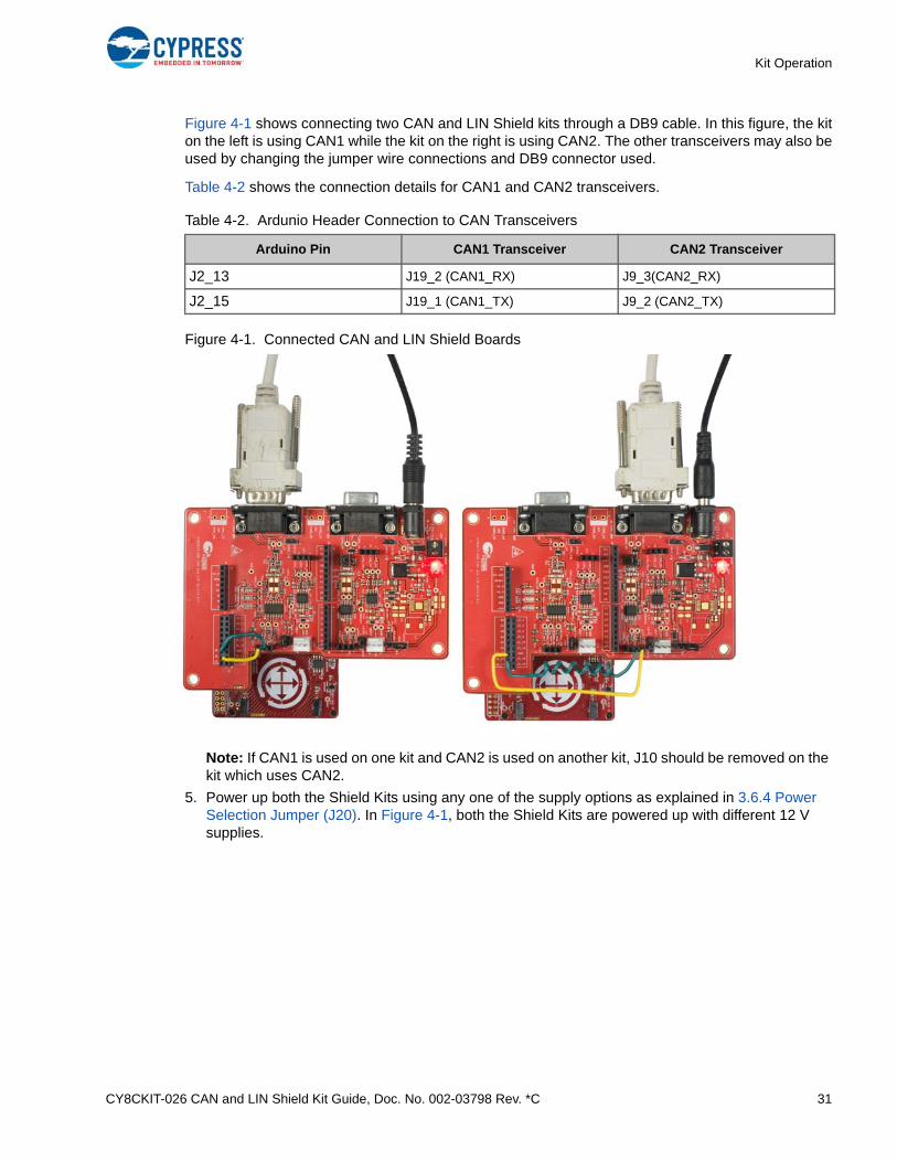
Figure 4-1 shows connecting two CAN and LIN Shield kits through a DB9 cable. In this figure, the kiton the left is using CAN1 while the kit on the right is using CAN2. The other transceivers may also beused by changing the jumper wire connections and DB9 connector used.
Table 4-2 shows the connection details for CAN1 and CAN2 transceivers.
Figure 4-1. Connected CAN and LIN Shield Boards
Note: If CAN1 is used on one kit and CAN2 is used on another kit, J10 should be removed on the kit which uses CAN2.
5. Power up both the Shield Kits using any one of the supply options as explained in 3.6.4 Power Selection Jumper (J20). In Figure 4-1, both the Shield Kits are powered up with different 12 V supplies.
Table 4-2. Ardunio Header Connection to CAN Transceivers
Arduino Pin CAN1 Transceiver CAN2 Transceiver
J2_13 J19_2 (CAN1_RX) J9_3(CAN2_RX)
J2_15 J19_1 (CAN1_TX) J9_2 (CAN2_TX)
CY8CKIT-026 CAN and LIN Shield Kit Guide, Doc. No. 002-03798 Rev. *C 32
Kit Operation
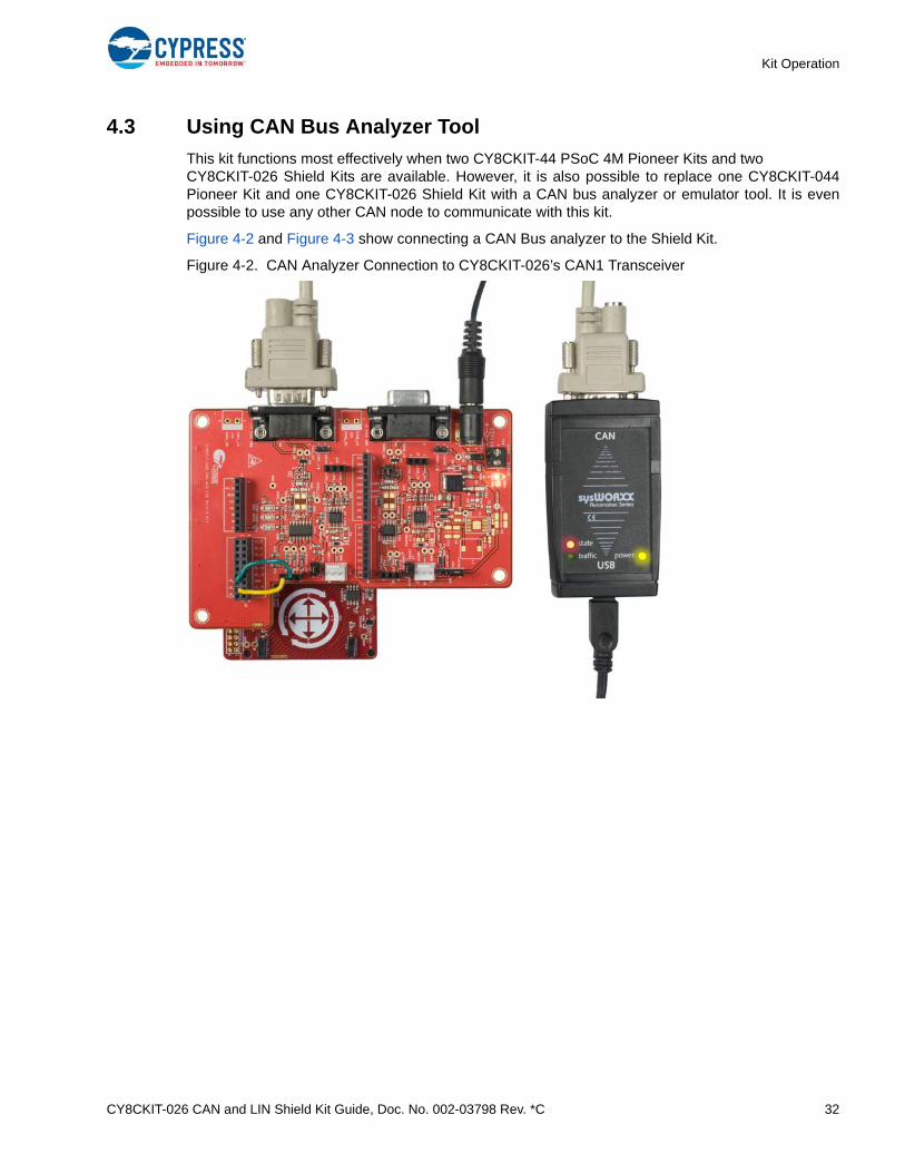
4.3 Using CAN Bus Analyzer Tool
This kit functions most effectively when two CY8CKIT-44 PSoC 4M Pioneer Kits and two CY8CKIT-026 Shield Kits are available. However, it is also possible to replace one CY8CKIT-044Pioneer Kit and one CY8CKIT-026 Shield Kit with a CAN bus analyzer or emulator tool. It is evenpossible to use any other CAN node to communicate with this kit.
Figure 4-2 and Figure 4-3 show connecting a CAN Bus analyzer to the Shield Kit.
Figure 4-2. CAN Analyzer Connection to CY8CKIT-026’s CAN1 Transceiver
CY8CKIT-026 CAN and LIN Shield Kit Guide, Doc. No. 002-03798 Rev. *C 33
Kit Operation
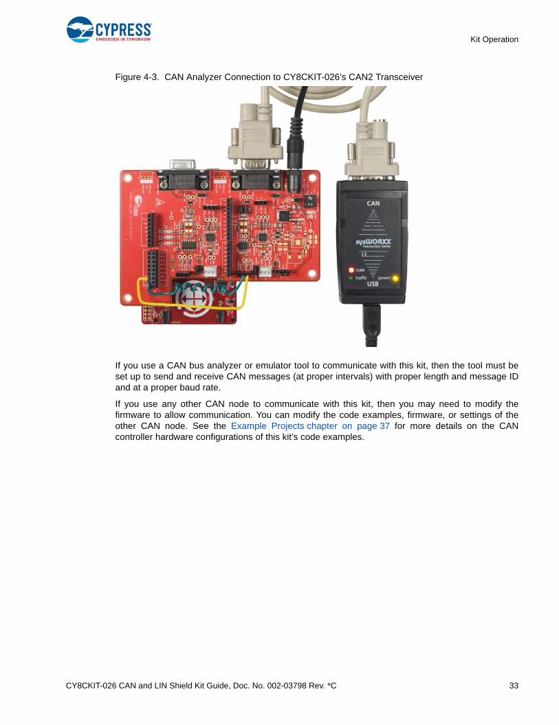
Figure 4-3. CAN Analyzer Connection to CY8CKIT-026’s CAN2 Transceiver
If you use a CAN bus analyzer or emulator tool to communicate with this kit, then the tool must beset up to send and receive CAN messages (at proper intervals) with proper length and message IDand at a proper baud rate.
If you use any other CAN node to communicate with this kit, then you may need to modify thefirmware to allow communication. You can modify the code examples, firmware, or settings of theother CAN node. See the Example Projects chapter on page 37 for more details on the CANcontroller hardware configurations of this kit’s code examples.
CY8CKIT-026 CAN and LIN Shield Kit Guide, Doc. No. 002-03798 Rev. *C 34
Kit Operation
4.4 LIN Communication Hardware Setup1. Connect the CAN and LIN Shield Kit to the Arduino header of the CY8CKIT-044/042 Pioneer Kit,
as shown in Figure 1-2.
2. Connect the LIN TX, LIN RX pins and Enable/sleep control pin (GPIO) of the controller (comes from the baseboard via the Arduino header) to LINx_TX, LINx_RX and LINx_NSLP pins (on J15 connector for LIN1 transceiver, J6 connector of LIN2 transceiver) of the LIN transceiver circuit using connecting wires. Table 4-3 shows how to connect the Arduino pins to the LINx transceiver using wires.
These connection are only if you are using P4.0 and P4.1 as LIN pins on the microcontroller. If you are using different pins for LIN, the corresponding pin connections on the Arduino header must be changed.
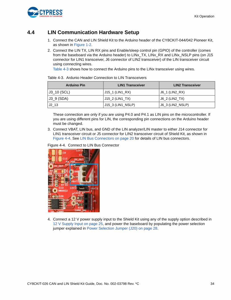
3. Connect VBAT, LIN bus, and GND of the LIN analyzer/LIN master to either J14 connector for LIN1 transceiver circuit or J5 connector for LIN2 transceiver circuit of Shield Kit, as shown in Figure 4-4. See LIN Bus Connectors on page 20 for details of LIN bus connectors.
Figure 4-4. Connect to LIN Bus Connector
4. Connect a 12 V power supply input to the Shield Kit using any of the supply option described in 12 V Supply Input on page 25, and power the baseboard by populating the power selection jumper explained in Power Selection Jumper (J20) on page 28.
Table 4-3. Ardunio Header Connection to LIN Transceivers
Arduino Pin LIN1 Transceiver LIN2 Transceiver
J3_10 (SCL) J15_1 (LIN1_RX) J6_1 (LIN2_RX)
J3_9 (SDA) J15_2 (LIN1_TX) J6_2 (LIN2_TX)
J2_13 J15_3 (LIN1_NSLP) J6_3 (LIN2_NSLP)
CY8CKIT-026 CAN and LIN Shield Kit Guide, Doc. No. 002-03798 Rev. *C 35
Kit Operation
4.5 Using LIN Bus Analyzer Tool
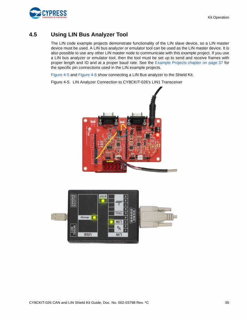
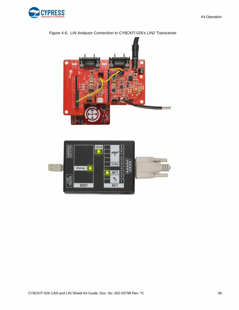
The LIN code example projects demonstrate functionality of the LIN slave device, so a LIN masterdevice must be used. A LIN bus analyzer or emulator tool can be used as the LIN master device. It isalso possible to use any other LIN master node to communicate with this example project. If you usea LIN bus analyzer or emulator tool, then the tool must be set up to send and receive frames withproper length and ID and at a proper baud rate. See the Example Projects chapter on page 37 forthe specific pin connections used in the LIN example projects.
Figure 4-5 and Figure 4-6 show connecting a LIN Bus analyzer to the Shield Kit.
Figure 4-5. LIN Analyzer Connection to CY8CKIT-026’s LIN1 Transceiver
CY8CKIT-026 CAN and LIN Shield Kit Guide, Doc. No. 002-03798 Rev. *C 36
Kit Operation
Figure 4-6. LIN Analyzer Connection to CY8CKIT-026’s LIN2 Transceiver
CY8CKIT-026 CAN and LIN Shield Kit Guide, Doc. No. 002-03798 Rev. *C 37
5. Example Projects
The CY8CKIT-026 CAN and LIN Shield Kit includes five example projects. This chapter explainshow to use these example projects. To access the example projects, download and install theCY8CKIT-026 CAN and LIN Shield Kit setup file from www.cypress.com/CY8CKIT-026. Afterinstallation, the kit example projects will be available in the Firmware folder in the installationlocation.
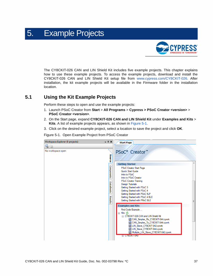
5.1 Using the Kit Example Projects
Perform these steps to open and use the example projects:
1. Launch PSoC Creator from Start > All Programs > Cypress > PSoC Creator <version> > PSoC Creator <version>.
2. On the Start page, expand CY8CKIT-026 CAN and LIN Shield Kit under Examples and Kits > Kits. A list of example projects appears, as shown in Figure 5-1.
3. Click on the desired example project, select a location to save the project and click OK.
Figure 5-1. Open Example Project from PSoC Creator
CY8CKIT-026 CAN and LIN Shield Kit Guide, Doc. No. 002-03798 Rev. *C 38
Example Projects
4. Build the example project by choosing Build > Build <Project Name>. A .hex file is generated after successful build process.
5. Connect the corresponding baseboard to the PC using the USB cable to program the kit with this example project.
6. Choose Debug > Program in PSoC Creator.
5.2 CAN_Simplex_Tx_CY8CKIT-044
5.2.1 Project Description
This project explains how to transmit data over the CAN bus. The device is configured as a CANtransmitter which transmits the data whenever the CapSense gesture pad is touched. When theCapSense gesture pad center button is pressed, then the blue LED on the baseboard (CY8CKIT-044) toggles (ON/OFF) and the CAN data byte1 also toggles between 0 and 1. If the left/rightbuttons of the gesture pad are pressed, then the CAN data byte2 toggles between 0, 1 and 2. If theup/down gesture pad is pressed, then the byte3 of the CAN data increases/decreases by 30 countsrespectively.
5.2.2 Hardware Connections
1. Plug-in the CY8CKIT-026 kit to the CY8CKIT-044 through Arduino connector.
2. Since there are two CAN transceivers on the CY8CKIT-026, choose to use one of the CAN transceivers (U6 - CAN1 and U4 - CAN2). Connect J2_13 and J2_15 to the appropriate CANx_Rx and CANx_Tx pins of the transceiver connector (J19 - CAN1 or J9 - CAN2), as provided in Table 5-1.
3. CAN2 transceiver works with 5 V, whereas CAN1 transceiver requires 12 V input supply.
4. If you have chosen CAN1 transceiver, then external 12 V supply has to be connected through J11, J12, or J17. Refer to Power Supply Configurations on page 24 for more details on power supply connections.
5. If you have chosen CAN2 transceiver, you can use external 12 V supply which will be converted to 5 V with the on board regulator, or you can power the CAN2 transceiver with the baseboard (CY8CKIT-044) by shorting pin 1 and 2 of the power selection jumper (J20).
6. When you are powering the CY8CKIT-026 with the baseboard with 5 V, ensure that the jumper J9 on the baseboard (CY8CKIT-044) is in the 5 V position. When you are using 12 V external supply and powering the baseboard from the Shield Kit (without a USB connection), ensure that the jumper J9 on the baseboard (CY8CKIT-044) is in the 3.3 V position. Refer to Power Selection Jumper (J20) on page 28 for more details.
7. Connect the CAN analyzer to the appropriate transceiver using a DB9 male to female connector as shown in Figure 4-2 or Figure 4-3 for receiving the transmitted data.
8. You can also use another CY8CKIT-044 and CY8CKIT-026 setup instead of a CAN analyzer as shown in Figure 4-1, which should be programmed with the CAN_Simplex_Rx_CY8CKIT-044 project (see CAN_Simplex_Rx_CY8CKIT-044 on page 41) to receive this transmitted data.
Table 5-1. Pin Connection on CY8CKIT-026
Arduino Header Pins CAN1 Transceiver CAN2 Transceiver
J2_13 J19_2 (CAN1_RX) J9_3 (CAN2_RX)
J2_15 J19_1 (CAN1_TX) J9_2 (CAN2_TX)
CY8CKIT-026 CAN and LIN Shield Kit Guide, Doc. No. 002-03798 Rev. *C 39
Example Projects
5.2.3 Verify Output
To verify the CAN_Simplex_Tx_CY8CKIT-044 example project, perform these steps:
1. Program the CY8CKIT-044 PSoC 4 M-Series Pioneer Kit with CAN_Simplex_Tx_CY8CKIT-044 code example through USB connector J6.
2. Ensure that the power supply and jumper settings are proper, as explained in the Hardware Connections on page 38.
3. Perform these steps if you are using any CAN analyzer for receiving the data:
a. Install the appropriate software of the CAN analyzer.
b. Open the CAN analyzer software and set the Baud rate to 125 Kbps.
c. Touch the CapSense gesture pad buttons (Center/Right/Left/Up/Down) and observe the data on CAN analyzer software, as provided in Table 5-2.
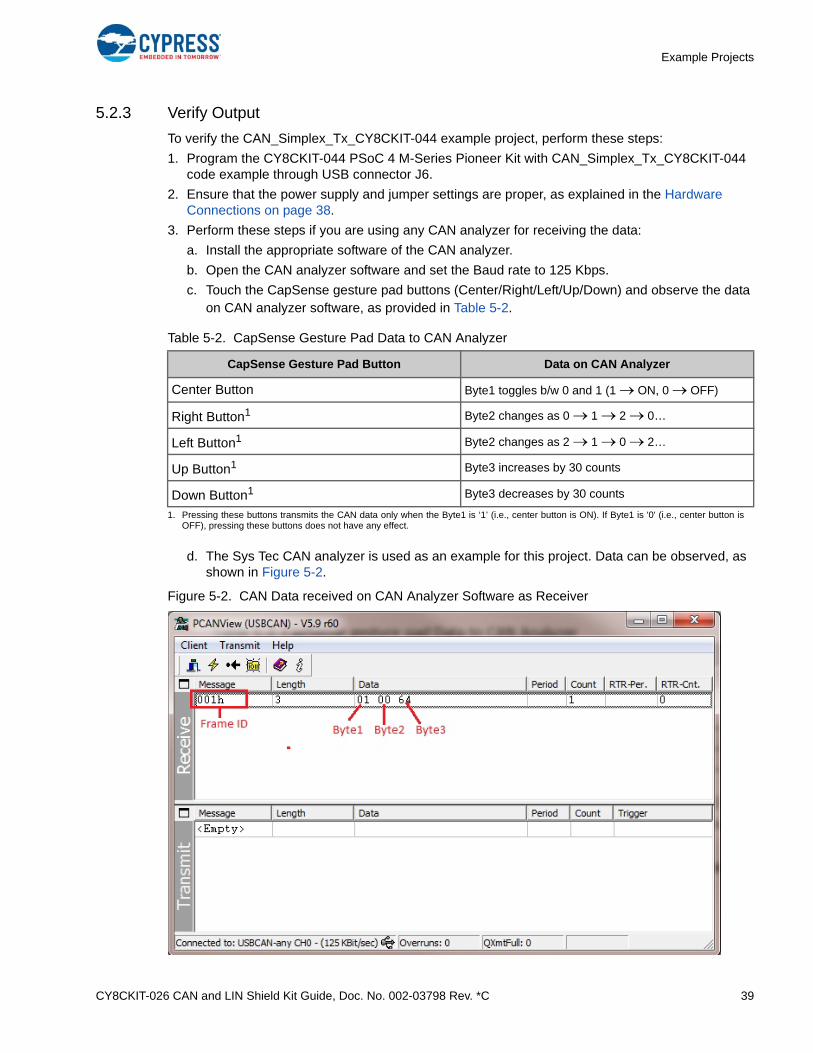
d. The Sys Tec CAN analyzer is used as an example for this project. Data can be observed, as shown in Figure 5-2.
Figure 5-2. CAN Data received on CAN Analyzer Software as Receiver
Table 5-2. CapSense Gesture Pad Data to CAN Analyzer
CapSense Gesture Pad Button Data on CAN Analyzer
Center Button Byte1 toggles b/w 0 and 1 (1 ON, 0 OFF)
Right Button1
1. Pressing these buttons transmits the CAN data only when the Byte1 is ‘1’ (i.e., center button is ON). If Byte1 is '0' (i.e., center button isOFF), pressing these buttons does not have any effect.
Byte2 changes as 0 1 2 0…
Left Button1 Byte2 changes as 2 1 0 2…
Up Button1 Byte3 increases by 30 counts
Down Button1 Byte3 decreases by 30 counts
CY8CKIT-026 CAN and LIN Shield Kit Guide, Doc. No. 002-03798 Rev. *C 40
Example Projects
4. Perform these steps, if you are using another set of CY8CKIT-044 and CY8CKIT-026 for receiving the data:
a. Program the second baseboard with the CAN_Simplex_Rx_CY8CKIT-044.hex file and set the hardware connections provided in Hardware Connections on page 41.
b. Connect both the Shield Kits with a DB9 male-to-male connector, as shown in Figure 4-1 and switch ON the power supply for both the kits.
c. Touch the CapSense gesture pad buttons on the first baseboard (that is programmed with CAN_Simplex_Tx_CY8CKIT-044 project). Observe the Color and Brightness of the RGB LED on the second board, as provided in Table 5-3.
5. To observe the data that is transmitted through CAN bus using UART, connect the baseboard to a PC using a USB cable, and then perform these steps:
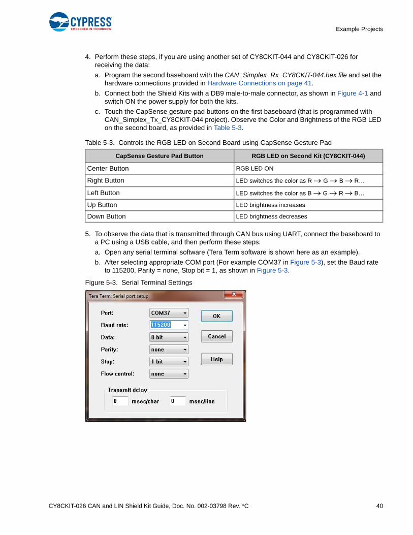
a. Open any serial terminal software (Tera Term software is shown here as an example).
b. After selecting appropriate COM port (For example COM37 in Figure 5-3), set the Baud rate to 115200, Parity = none, Stop bit = 1, as shown in Figure 5-3.
Figure 5-3. Serial Terminal Settings
Table 5-3. Controls the RGB LED on Second Board using CapSense Gesture Pad
CapSense Gesture Pad Button RGB LED on Second Kit (CY8CKIT-044)
Center Button RGB LED ON
Right Button LED switches the color as R G B R…
Left Button LED switches the color as B G R B…
Up Button LED brightness increases
Down Button LED brightness decreases
CY8CKIT-026 CAN and LIN Shield Kit Guide, Doc. No. 002-03798 Rev. *C 41
Example Projects
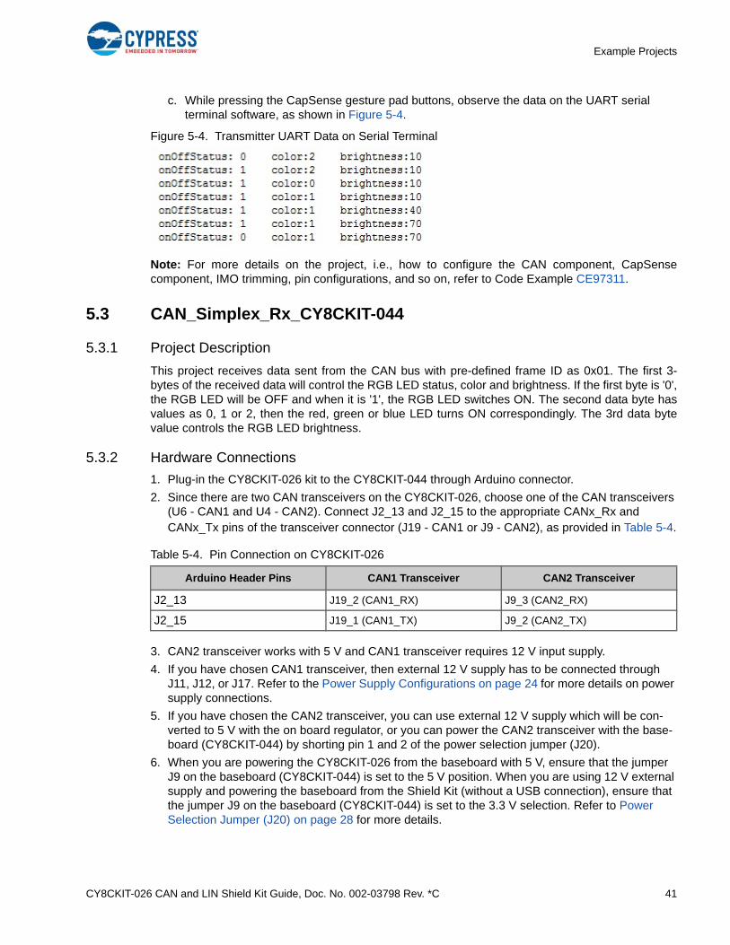
c. While pressing the CapSense gesture pad buttons, observe the data on the UART serial terminal software, as shown in Figure 5-4.
Figure 5-4. Transmitter UART Data on Serial Terminal
Note: For more details on the project, i.e., how to configure the CAN component, CapSensecomponent, IMO trimming, pin configurations, and so on, refer to Code Example CE97311.
5.3 CAN_Simplex_Rx_CY8CKIT-044
5.3.1 Project Description
This project receives data sent from the CAN bus with pre-defined frame ID as 0x01. The first 3-bytes of the received data will control the RGB LED status, color and brightness. If the first byte is '0',the RGB LED will be OFF and when it is '1', the RGB LED switches ON. The second data byte hasvalues as 0, 1 or 2, then the red, green or blue LED turns ON correspondingly. The 3rd data bytevalue controls the RGB LED brightness.
5.3.2 Hardware Connections
1. Plug-in the CY8CKIT-026 kit to the CY8CKIT-044 through Arduino connector.
2. Since there are two CAN transceivers on the CY8CKIT-026, choose one of the CAN transceivers (U6 - CAN1 and U4 - CAN2). Connect J2_13 and J2_15 to the appropriate CANx_Rx and CANx_Tx pins of the transceiver connector (J19 - CAN1 or J9 - CAN2), as provided in Table 5-4.
3. CAN2 transceiver works with 5 V and CAN1 transceiver requires 12 V input supply.
4. If you have chosen CAN1 transceiver, then external 12 V supply has to be connected through J11, J12, or J17. Refer to the Power Supply Configurations on page 24 for more details on power supply connections.
5. If you have chosen the CAN2 transceiver, you can use external 12 V supply which will be con-verted to 5 V with the on board regulator, or you can power the CAN2 transceiver with the base-board (CY8CKIT-044) by shorting pin 1 and 2 of the power selection jumper (J20).
6. When you are powering the CY8CKIT-026 from the baseboard with 5 V, ensure that the jumper J9 on the baseboard (CY8CKIT-044) is set to the 5 V position. When you are using 12 V external supply and powering the baseboard from the Shield Kit (without a USB connection), ensure that the jumper J9 on the baseboard (CY8CKIT-044) is set to the 3.3 V selection. Refer to Power Selection Jumper (J20) on page 28 for more details.
Table 5-4. Pin Connection on CY8CKIT-026
Arduino Header Pins CAN1 Transceiver CAN2 Transceiver
J2_13 J19_2 (CAN1_RX) J9_3 (CAN2_RX)
J2_15 J19_1 (CAN1_TX) J9_2 (CAN2_TX)
CY8CKIT-026 CAN and LIN Shield Kit Guide, Doc. No. 002-03798 Rev. *C 42
Example Projects
7. Connect the CAN analyzer to the appropriate transceiver using a DB9 male to female connector, as shown in Figure 4-2 or Figure 4-3 for receiving the transmitted data.
8. You can also use another CY8CKIT-044 and CY8CKIT-026 setup instead of a CAN analyzer, as shown in Figure 4-1, which should be programmed with the CAN_Simplex_Tx_CY8CKIT-044 project (described above) to transmit data over CAN.
5.3.3 Verify Output
To verify the CAN_Simplex_Rx_CY8CKIT-044 code example, perform these steps:
1. Program the CY8CKIT-044 PSoC 4 M-Series Pioneer Kit with CAN_Simplex_Rx_CY8CKIT-044 code example through USB connector J6.
2. Make sure that the power supply and jumper settings are proper as explained in the Hardware Connections on page 41.
3. Perform these steps if you are using any CAN analyzer for receiving the data:
a. Install the appropriate software of the CAN analyzer.
b. Open the CAN analyzer software and set the Baud rate to 125 Kbps.
c. Add a new transmit frame as, Frame ID = 0x01, Data Length Code (DLC) 3, and add data bytes values as provided in Table 5-5.
Table 5-5. RGB LED Status with respect to CAN Data Bytes
Data BytesRGB LED Status on CY8CKIT-044
Byte Number Value
Byte ‘1’0 LED OFF
1 LED ON
Byte ‘2’
01
1. Transmitting these values changes the RGB LED color and brightness only when the first data byte is equal to '1'. If the Byte1 is '0',sending these values doesn't have any effect on the RGB LED status & brightness
Red LED ON
11 Green LED ON
21 Blue LED ON
Byte ‘3’ 0 to 2551 Controls the brightness of the LED
CY8CKIT-026 CAN and LIN Shield Kit Guide, Doc. No. 002-03798 Rev. *C 43
Example Projects
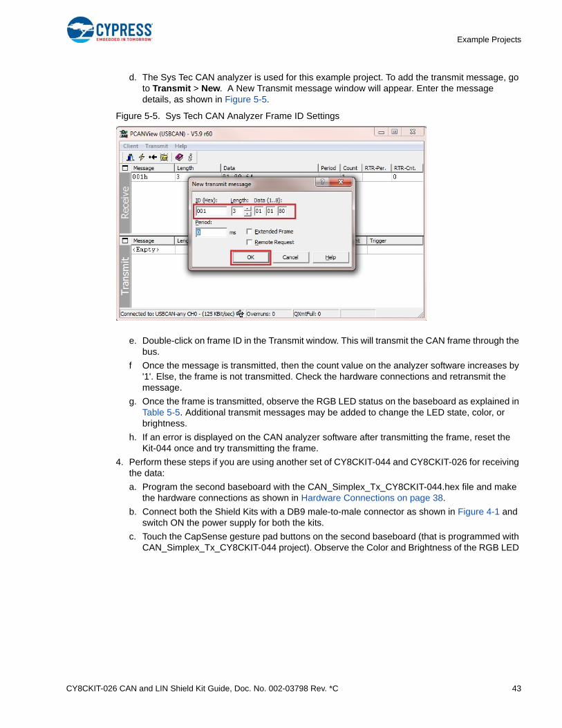
d. The Sys Tec CAN analyzer is used for this example project. To add the transmit message, go to Transmit > New. A New Transmit message window will appear. Enter the message details, as shown in Figure 5-5.
Figure 5-5. Sys Tech CAN Analyzer Frame ID Settings
e. Double-click on frame ID in the Transmit window. This will transmit the CAN frame through the bus.
f Once the message is transmitted, then the count value on the analyzer software increases by '1'. Else, the frame is not transmitted. Check the hardware connections and retransmit the message.
g. Once the frame is transmitted, observe the RGB LED status on the baseboard as explained in Table 5-5. Additional transmit messages may be added to change the LED state, color, or brightness.
h. If an error is displayed on the CAN analyzer software after transmitting the frame, reset the Kit-044 once and try transmitting the frame.
4. Perform these steps if you are using another set of CY8CKIT-044 and CY8CKIT-026 for receiving the data:
a. Program the second baseboard with the CAN_Simplex_Tx_CY8CKIT-044.hex file and make the hardware connections as shown in Hardware Connections on page 38.
b. Connect both the Shield Kits with a DB9 male-to-male connector as shown in Figure 4-1 and switch ON the power supply for both the kits.
c. Touch the CapSense gesture pad buttons on the second baseboard (that is programmed with CAN_Simplex_Tx_CY8CKIT-044 project). Observe the Color and Brightness of the RGB LED
CY8CKIT-026 CAN and LIN Shield Kit Guide, Doc. No. 002-03798 Rev. *C 44
Example Projects
on the second board, as provided in Table 5-6.
5. To observe the data received through CAN bus using UART, connect the baseboard to the PC through USB cable and perform these steps:
a. Open any serial terminal software (Tera Term software is used an example here).
b. After selecting appropriate COM port (For example COM37 in Figure 5-3), set the Baud rate to 115200, Parity = none, Stop bit = 1, as shown in Figure 5-3.
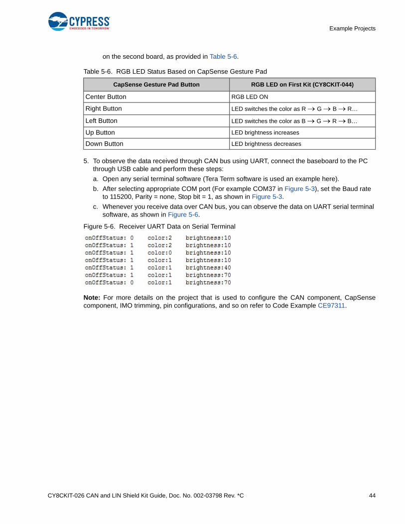
c. Whenever you receive data over CAN bus, you can observe the data on UART serial terminal software, as shown in Figure 5-6.
Figure 5-6. Receiver UART Data on Serial Terminal
Note: For more details on the project that is used to configure the CAN component, CapSensecomponent, IMO trimming, pin configurations, and so on refer to Code Example CE97311.
Table 5-6. RGB LED Status Based on CapSense Gesture Pad
CapSense Gesture Pad Button RGB LED on First Kit (CY8CKIT-044)
Center Button RGB LED ON
Right Button LED switches the color as R G B R…
Left Button LED switches the color as B G R B…
Up Button LED brightness increases
Down Button LED brightness decreases
CY8CKIT-026 CAN and LIN Shield Kit Guide, Doc. No. 002-03798 Rev. *C 45
Example Projects
5.4 LIN_Slave_CY8CKIT-042
5.4.1 Project Description
In this example, PSoC 4200 (CY8CKIT-042) acts as a simple LIN slave. The slave monitors datathat is transmitted from the LIN master (analyzer). If a predefined frame is received from the master,the slave controls the RGB LED color according to the data available in the received frame. The LINmaster can get the RGB LED status by sending a frame with a predefined frame ID.
5.4.2 Hardware Connections
1. Plug-in the CY8CKIT-026 kit to the CY8CKIT-042 using the Arduino connectors.
2. Since there are two LIN transceivers on the CY8CKIT-026, choose either of the transceivers to use (U5 - LIN1 transceiver or U3 - LIN2 transceiver). Connect the Arduino header pins (which are connected to the baseboard controller) to the appropriate LIN transceiver using jumper wires, as provided in Table 5-7.
3. Connect the LIN analyzer to the J14 connector to use LIN1 transceiver or J5 connector to use LIN2 transceiver
4. If the LIN analyzer DOES provide 12 V supply through the VBAT pin then you can power the board with that supply without using any additional 12 V supply since the corresponding jumper (J16 for LIN1 & J7 for LIN2) are populated by default.
5. You need to connect a 12 V supply input to the board through J11 power jack or J12 screw termi-nal connector, if the analyzer DOES NOT provides 12 V supply.
6. The baseboard (CY8CKIT-042) can be powered using USB or it can be powered from the Shield kit by selecting jumper J20 appropriately. Refer to the Power Selection Jumper (J20) on page 28 for more details on power connection options.
Table 5-7. Pin Connection on CY8CKIT-026
Arduino Header Pins LIN1 Transceiver LIN2 Transceiver
J3_10 (SCL) J15_1 (LIN1_RX) J6_1 (LIN2_RX)
J3_9 (SDA) J15_2 (LIN1_TX) J6_2 (LIN2_TX)
J2_13 J15_3 (LIN1_NSLP) J6_3 (LIN2_NSLP)
Caution: Ensure extra care when the LIN analyzer provides 12 V through the VBAT pin and con-necting it to any of the connectors J14 and J5 and also using a 12 V external supply. Since the jumpers J16 and J7 are populated (by default); it will short the VIN supply rail to the VBAT pin of the LIN connector. In that case, either remove the external 12 V supply or remove the correspond-ing jumper (J16 or J7). Otherwise, the Shield Kit, Baseboard and supply adapter could be dam-aged.
CY8CKIT-026 CAN and LIN Shield Kit Guide, Doc. No. 002-03798 Rev. *C 46
Example Projects
5.4.3 Verify Output
To verify the LIN_Slave_CY8CKIT-042 code example, perform these steps.
Silicon Engines LIN/USB Data Converter is used as LIN analyzer in this example.
1. Program the CY8CKIT-042 PSoC 4 Pioneer Kit with LIN_Slave_CY8CKIT-042 example project through USB connector J10.
2. Ensure that the power supply and jumper settings are as explained in 5.4.2 Hardware Connections.
3. Install the 'SE9004 and 9011 LINUSB Message Center software (provided by Silicon Engines) on your PC and connect the LIN analyzer to PC through USB cable. If a different analyzer is being used, install the appropriate software.
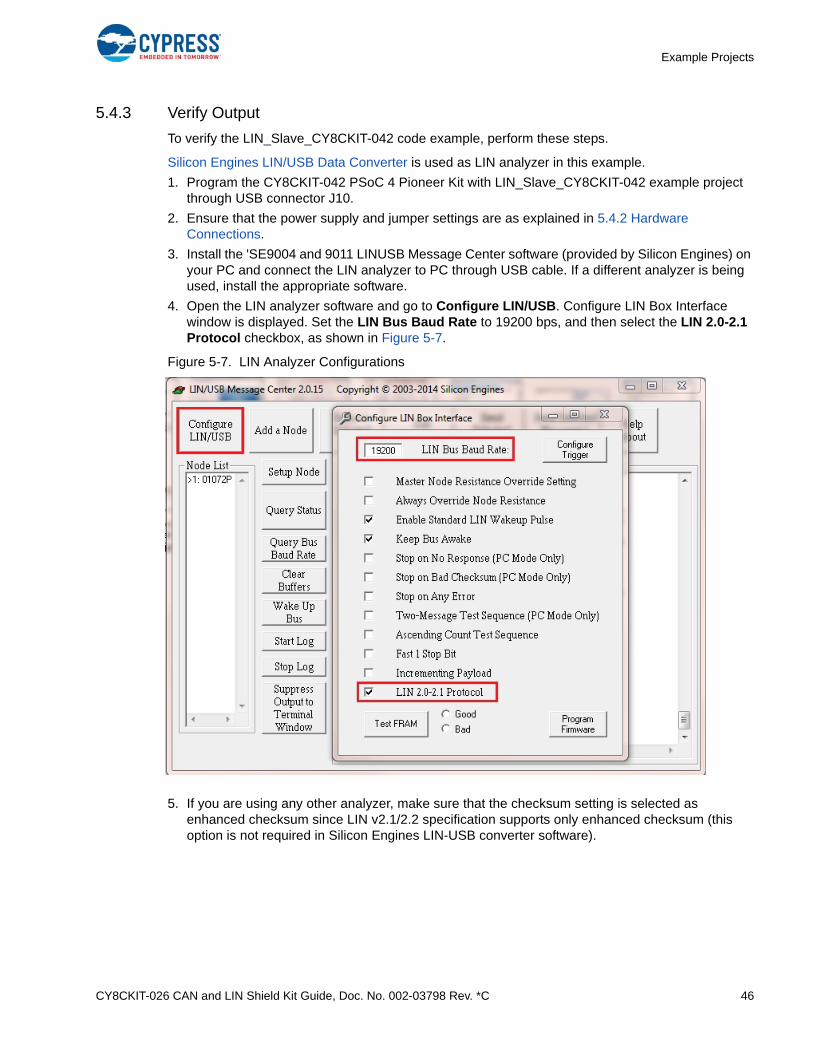
4. Open the LIN analyzer software and go to Configure LIN/USB. Configure LIN Box Interface window is displayed. Set the LIN Bus Baud Rate to 19200 bps, and then select the LIN 2.0-2.1 Protocol checkbox, as shown in Figure 5-7.
Figure 5-7. LIN Analyzer Configurations
5. If you are using any other analyzer, make sure that the checksum setting is selected as enhanced checksum since LIN v2.1/2.2 specification supports only enhanced checksum (this option is not required in Silicon Engines LIN-USB converter software).
CY8CKIT-026 CAN and LIN Shield Kit Guide, Doc. No. 002-03798 Rev. *C 47
Example Projects
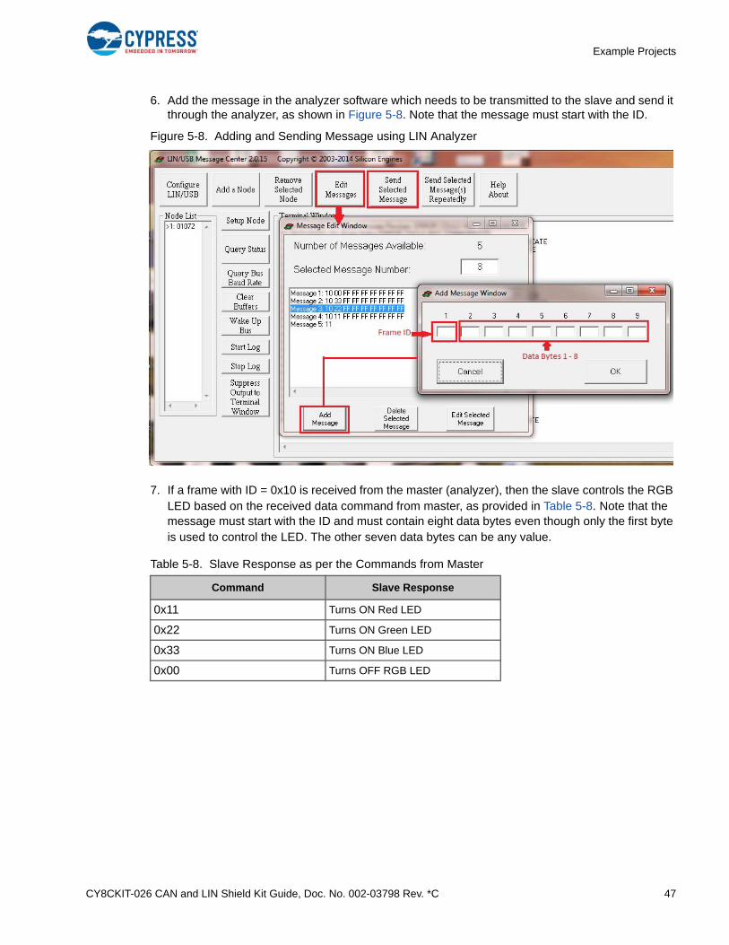
6. Add the message in the analyzer software which needs to be transmitted to the slave and send it through the analyzer, as shown in Figure 5-8. Note that the message must start with the ID.
Figure 5-8. Adding and Sending Message using LIN Analyzer
7. If a frame with ID = 0x10 is received from the master (analyzer), then the slave controls the RGB LED based on the received data command from master, as provided in Table 5-8. Note that the message must start with the ID and must contain eight data bytes even though only the first byte is used to control the LED. The other seven data bytes can be any value.
Table 5-8. Slave Response as per the Commands from Master
Command Slave Response
0x11 Turns ON Red LED
0x22 Turns ON Green LED
0x33 Turns ON Blue LED
0x00 Turns OFF RGB LED
CY8CKIT-026 CAN and LIN Shield Kit Guide, Doc. No. 002-03798 Rev. *C 48
Example Projects
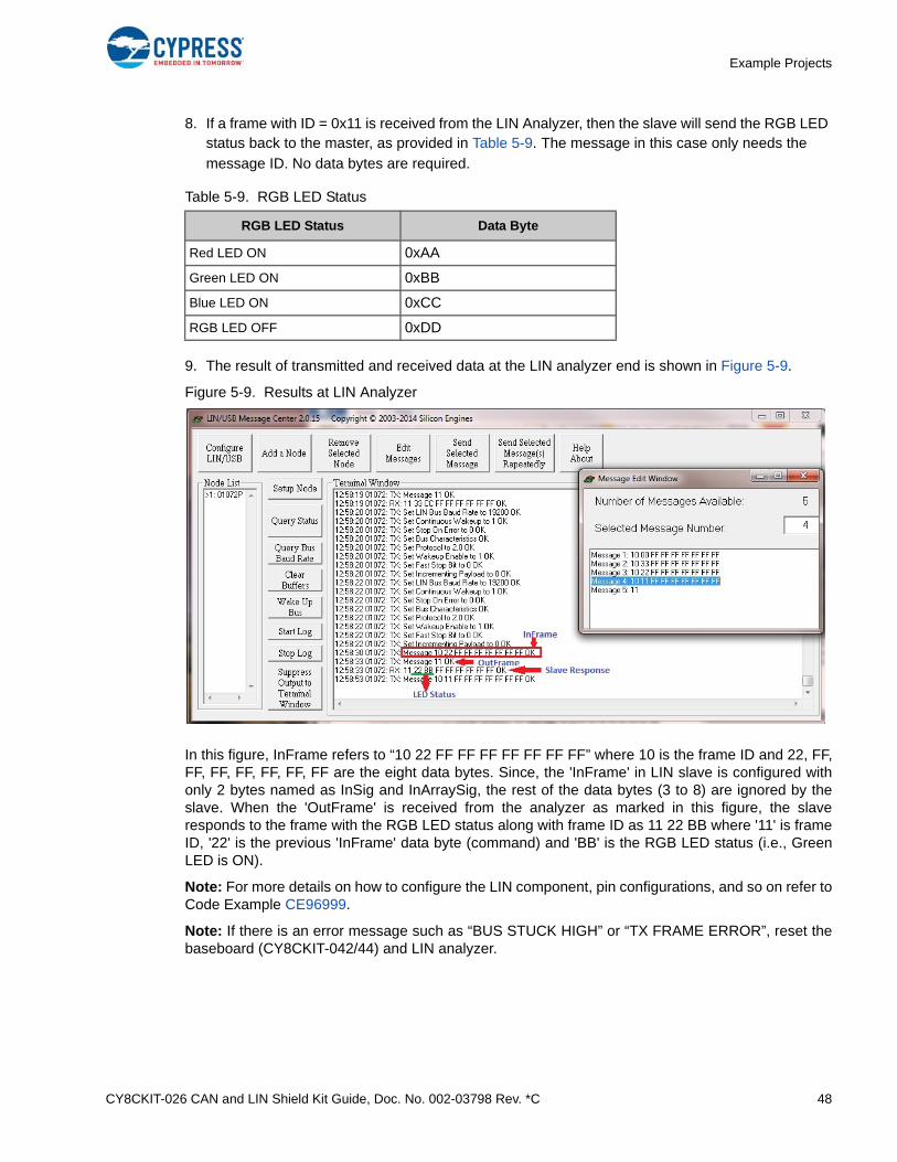
8. If a frame with ID = 0x11 is received from the LIN Analyzer, then the slave will send the RGB LED status back to the master, as provided in Table 5-9. The message in this case only needs the
message ID. No data bytes are required.
9. The result of transmitted and received data at the LIN analyzer end is shown in Figure 5-9.
Figure 5-9. Results at LIN Analyzer
In this figure, InFrame refers to “10 22 FF FF FF FF FF FF FF” where 10 is the frame ID and 22, FF,FF, FF, FF, FF, FF, FF are the eight data bytes. Since, the 'InFrame' in LIN slave is configured withonly 2 bytes named as InSig and InArraySig, the rest of the data bytes (3 to 8) are ignored by theslave. When the 'OutFrame' is received from the analyzer as marked in this figure, the slaveresponds to the frame with the RGB LED status along with frame ID as 11 22 BB where '11' is frameID, '22' is the previous 'InFrame' data byte (command) and 'BB' is the RGB LED status (i.e., GreenLED is ON).
Note: For more details on how to configure the LIN component, pin configurations, and so on refer toCode Example CE96999.
Note: If there is an error message such as “BUS STUCK HIGH” or “TX FRAME ERROR”, reset thebaseboard (CY8CKIT-042/44) and LIN analyzer.
Table 5-9. RGB LED Status
RGB LED Status Data Byte
Red LED ON 0xAA
Green LED ON 0xBB
Blue LED ON 0xCC
RGB LED OFF 0xDD
CY8CKIT-026 CAN and LIN Shield Kit Guide, Doc. No. 002-03798 Rev. *C 49
Example Projects
5.5 LIN_Slave_CY8CKIT-044
5.5.1 Project Description
In this example, PSoC 4200 M (CY8CKIT-044) acts as a simple LIN slave. The slave monitors datathat is transmitted from the LIN master (analyzer). If a predefined frame is received from the master,the slave controls the RGB LED color according to the data available in the received frame. The LINmaster can get the RGB LED status by sending a frame with a predefined frame ID.
The example project LIN_Slave_CY8CKIT-044 is same as LIN_Slave_CY8CKIT-042 except thebaseboard that is CY8CKIT-044 is used instead of CY8CKIT-042.
Follow the same steps for Hardware connections and verifying the output as specified in 5.4LIN_Slave_CY8CKIT-042 and replace the baseboard from CY8CKIT-042 to CY8CKIT-044.
Note: For more details on how to configure the LIN component, pin configurations, and so on refer toCode Example CE96999.
5.6 Multiple_LIN_Slave_CY8CKIT-042
5.6.1 Project Description
In this example, PSoC 4 is initialized as two LIN slave nodes; each node is connected to a differentLIN master. If a predefined frame is received from the LIN master1, the slave either stores or sendsthe CapSense linear slider centroid position to the master. If a predefined frame is received from theLIN master2, the slave either controls/changes the RGB LED or sends the RGB LED status to themaster. LIN1 is configured as a v2.0/2.1 slave while LIN2 is configured as a v1.3 slave.
5.6.2 Hardware Connections
1. Plug-in the CY8CKIT-026 kit to the CY8CKIT-042 using the Arduino connectors.
2. Connect the Arduino header pins (which are connected to the baseboard controller) to the appropriate LIN transceiver through jumper wires, as provided in Table 5-10.
3. Connect the LIN1 analyzer to the J14 connector and LIN2 analyzer to J5 connector on the CY8CKIT-026 Kit. Since there are two LIN slaves in this project, you need to have two LIN analyzers - each should connect to one LIN slave.
4. If either of the LIN analyzer DOES provide 12 V supply through VBAT pin then you can power the board with that supply without using any additional 12 V supply since the corresponding jumper (J16 for LIN1 and J7 for LIN2) are populated by default. Be careful to not power-up the shield kit with multiple supplies.
Table 5-10. Pin Connection on CY8CKIT-026
Arduino Header Pins LIN1 & LIN2 Connector Pins
J3_10 J15_1 (LIN1_RX)
J3_9 J15_2 (LIN1_TX)
J2_13 J15_3 (LIN1_NSLP)
D0 J6_1 (LIN2_RX)
D1 J6_2 (LIN2_TX)
J2_15 J6_3 (LIN2_NSLP)
CY8CKIT-026 CAN and LIN Shield Kit Guide, Doc. No. 002-03798 Rev. *C 50
Example Projects
5. You need to connect a 12 V supply input to the board through J11 power jack or J12 screw terminal connector, if both the analyzers DO NOT provide 12 V supply.
7. The baseboard (CY8CKIT-042) can be powered using USB or it can be powered from the Shield kit by selecting jumper J20 appropriately. Refer to the Power Selection Jumper (J20) on page 28 for more details on power connection options.
5.6.3 Verify Output
To verify the Multiple_LIN_Slave_CY8CKIT-042 example project, perform these steps:
In this example, the PSoC 4200 device is configured as two LIN slaves where each slave isconnected to a different LIN network. You need two LIN analyzers to verify the output. Two SiliconEngines LIN/USB Data Converter's are used as LIN analyzers in this example.
1. Program the CY8CKIT-042 PSoC 4 Pioneer Kit with Multiple_LIN_Slave_CY8CKIT-042 example project through USB connector J10.
2. Make sure that the power supply and jumper settings are proper as explained in the Hardware Connections on page 49.
3. Install the 'SE9004 and 9011 LINUSB Message Center' software (if a different analyzer is being used, install the appropriate software) on your PC and connect the LIN analyzer to PC through USB cable.
4. Verifying the LIN slave1 output:
a. Open the LIN1 analyzer software and go to Configure LIN/USB, set the LIN Bus Baud Rate to 19200 bps, and then select the LIN 2.0-2.1 Protocol checkbox as shown in Figure 5-7.
b. If you are using any other analyzer, make sure that the checksum setting is selected as enhanced checksum since LIN v2.1/2.2 specification supports only enhanced checksum (this option is not required in Silicon Engines LIN-USB converter software).
c. Add the message/frame in the analyzer software which needs to be transmitted to the slave and send it through the analyzer shown in Figure 5-8.
d. Place your finger on the CapSesne linear slider (on the CY8CKIT-042) and send a frame with ID = 0x10 and 8 data bytes. The first data byte should be 0x22. The other data bytes can be any value.
e. If a frame with ID = 0x10 with first data byte = 0x22 is received from LIN1 analyzer, then the slave will store the current CapSense linear slider centroid position.
f. If a frame with ID = 0x11 is received from the LIN1 analyzer, then the slave will send the stored CapSense linear slider centroid position back to the analyzer.
Caution: Ensure extra care when either of the LIN analyzers provide 12 V through VBAT pin and connecting it to any of the connectors J14 and J5 and also using 12 V external supply. Since the jumpers J16 and J7 are populated (by default), it will short the VIN supply rail to the VBAT pin of the LIN connector. In that case, either remove the external 12 V supply or remove the correspond-ing jumper (J16 or J7). Otherwise, the Shield Kit, Baseboard and supply adapter could be dam-aged.
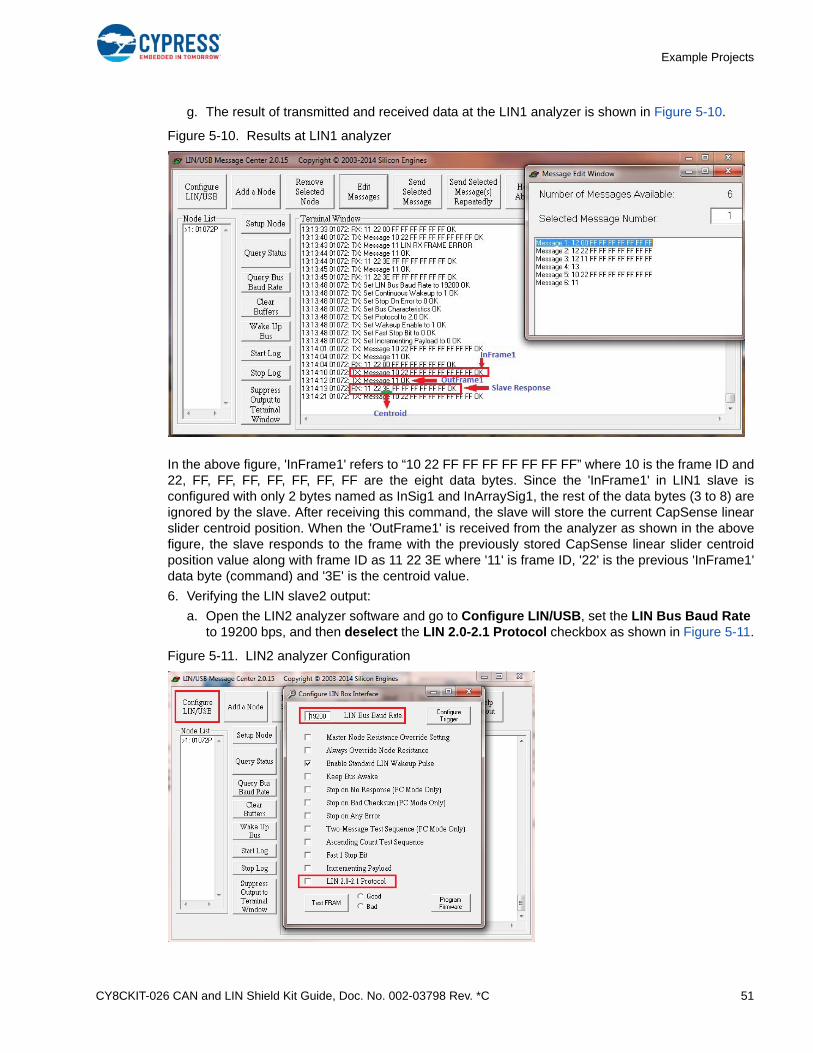
CY8CKIT-026 CAN and LIN Shield Kit Guide, Doc. No. 002-03798 Rev. *C 51
Example Projects
g. The result of transmitted and received data at the LIN1 analyzer is shown in Figure 5-10.
Figure 5-10. Results at LIN1 analyzer
In the above figure, 'InFrame1' refers to “10 22 FF FF FF FF FF FF FF” where 10 is the frame ID and22, FF, FF, FF, FF, FF, FF, FF are the eight data bytes. Since the 'InFrame1' in LIN1 slave isconfigured with only 2 bytes named as InSig1 and InArraySig1, the rest of the data bytes (3 to 8) areignored by the slave. After receiving this command, the slave will store the current CapSense linearslider centroid position. When the 'OutFrame1' is received from the analyzer as shown in the abovefigure, the slave responds to the frame with the previously stored CapSense linear slider centroidposition value along with frame ID as 11 22 3E where '11' is frame ID, '22' is the previous 'InFrame1'data byte (command) and '3E' is the centroid value.
6. Verifying the LIN slave2 output:
a. Open the LIN2 analyzer software and go to Configure LIN/USB, set the LIN Bus Baud Rate to 19200 bps, and then deselect the LIN 2.0-2.1 Protocol checkbox as shown in Figure 5-11.
Figure 5-11. LIN2 analyzer Configuration
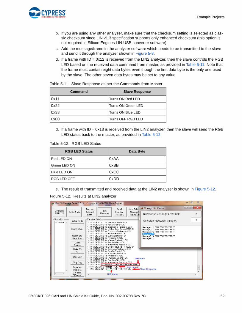
CY8CKIT-026 CAN and LIN Shield Kit Guide, Doc. No. 002-03798 Rev. *C 52
Example Projects
b. If you are using any other analyzer, make sure that the checksum setting is selected as clas-sic checksum since LIN v1.3 specification supports only enhanced checksum (this option is not required in Silicon Engines LIN-USB converter software).
c. Add the message/frame in the analyzer software which needs to be transmitted to the slave and send it through the analyzer shown in Figure 5-8.
d. If a frame with ID = 0x12 is received from the LIN2 analyzer, then the slave controls the RGB LED based on the received data command from master, as provided in Table 5-11. Note that the frame must contain eight data bytes even though the first data byte is the only one used by the slave. The other seven data bytes may be set to any value.
d. If a frame with ID = 0x13 is received from the LIN2 analyzer, then the slave will send the RGB LED status back to the master, as provided in Table 5-12.
e. The result of transmitted and received data at the LIN2 analyzer is shown in Figure 5-12.
Figure 5-12. Results at LIN2 analyzer
Table 5-11. Slave Response as per the Commands from Master
Command Slave Response
0x11 Turns ON Red LED
0x22 Turns ON Green LED
0x33 Turns ON Blue LED
0x00 Turns OFF RGB LED
Table 5-12. RGB LED Status
RGB LED Status Data Byte
Red LED ON 0xAA
Green LED ON 0xBB
Blue LED ON 0xCC
RGB LED OFF 0xDD

CY8CKIT-026 CAN and LIN Shield Kit Guide, Doc. No. 002-03798 Rev. *C 53
Example Projects
In Figure 5-12, ‘InFrame2’ refers to “12 11 FF FF FF FF FF FF FF” where 12 is the frame ID and 11,FF, FF, FF, FF, FF, FF, FF are the eight data bytes. Since, the ‘InFrame2’ in LIN slave2 is configuredwith only 2 bytes named as InSig2 and InArraySig2, the rest of the data bytes (3 to 8) are ignored bythe slave. When the ‘OutFrame2’ is received from the analyzer as marked in this figure, the slaveresponds to the frame with the RGB LED status along with frame ID as 13 11 AA where ‘13’ is frameID, ‘11’ is the previous ‘InFrame2’ data byte (command) and ‘AA’ is the RGB LED status (i.e., RedLED is ON).
Note: For more details on how to configure the LIN component, pin configurations, and so on refer toCode Example CE96999.
Note: If there is an error message such as “BUS STUCK HIGH” or “TX FRAME ERROR”, reset thebaseboard (CY8CKIT-042) and LIN analyzer.
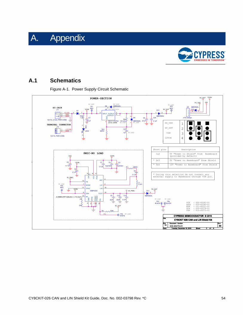
CY8CKIT-026 CAN and LIN Shield Kit Guide, Doc. No. 002-03798 Rev. *C 54
A. Appendix
A.1 Schematics
Figure A-1. Power Supply Circuit Schematic
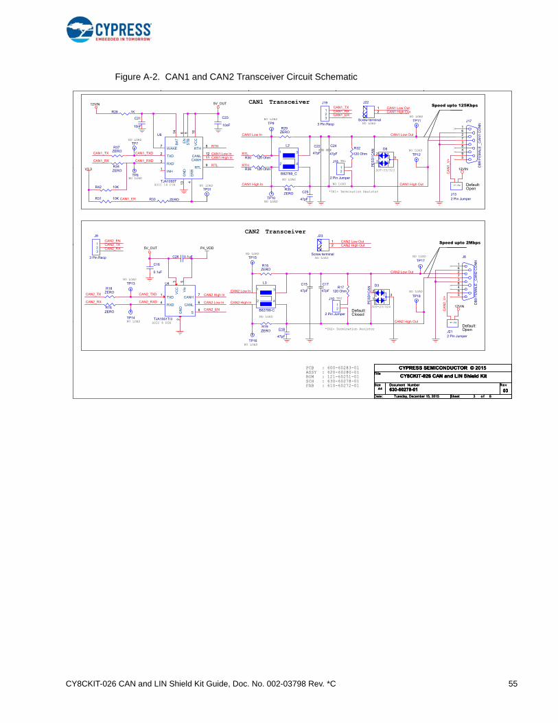
CY8CKIT-026 CAN and LIN Shield Kit Guide, Doc. No. 002-03798 Rev. *C 55
Figure A-2. CAN1 and CAN2 Transceiver Circuit Schematic
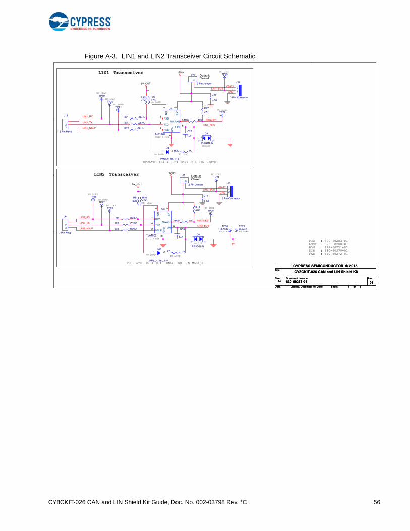
CY8CKIT-026 CAN and LIN Shield Kit Guide, Doc. No. 002-03798 Rev. *C 56
Figure A-3. LIN1 and LIN2 Transceiver Circuit Schematic
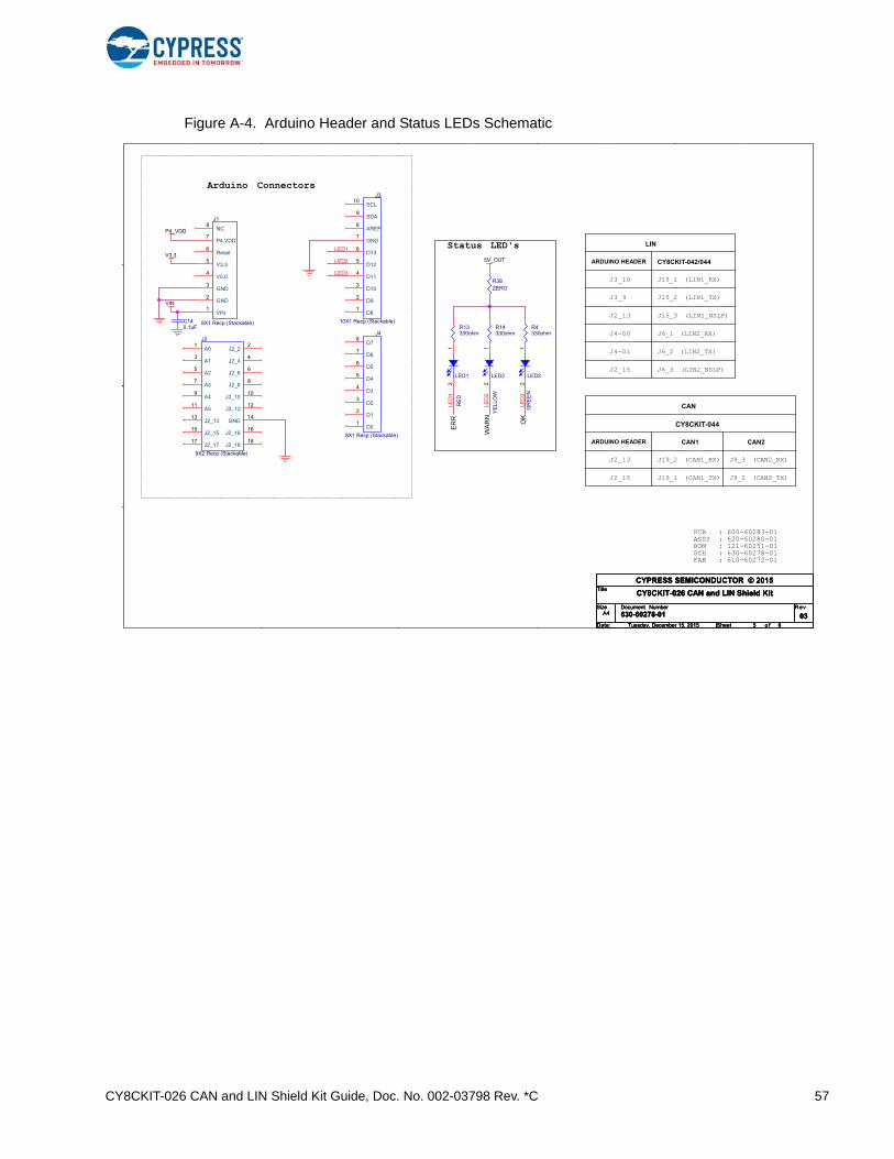
CY8CKIT-026 CAN and LIN Shield Kit Guide, Doc. No. 002-03798 Rev. *C 57
Figure A-4. Arduino Header and Status LEDs Schematic
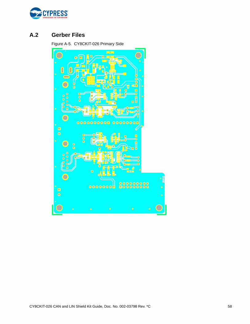
CY8CKIT-026 CAN and LIN Shield Kit Guide, Doc. No. 002-03798 Rev. *C 58
A.2 Gerber Files
Figure A-5. CY8CKIT-026 Primary Side
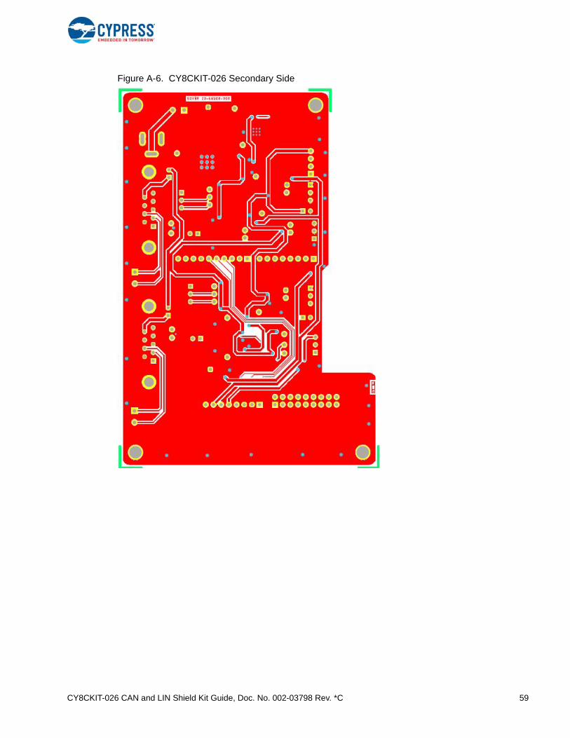
CY8CKIT-026 CAN and LIN Shield Kit Guide, Doc. No. 002-03798 Rev. *C 59
Figure A-6. CY8CKIT-026 Secondary Side
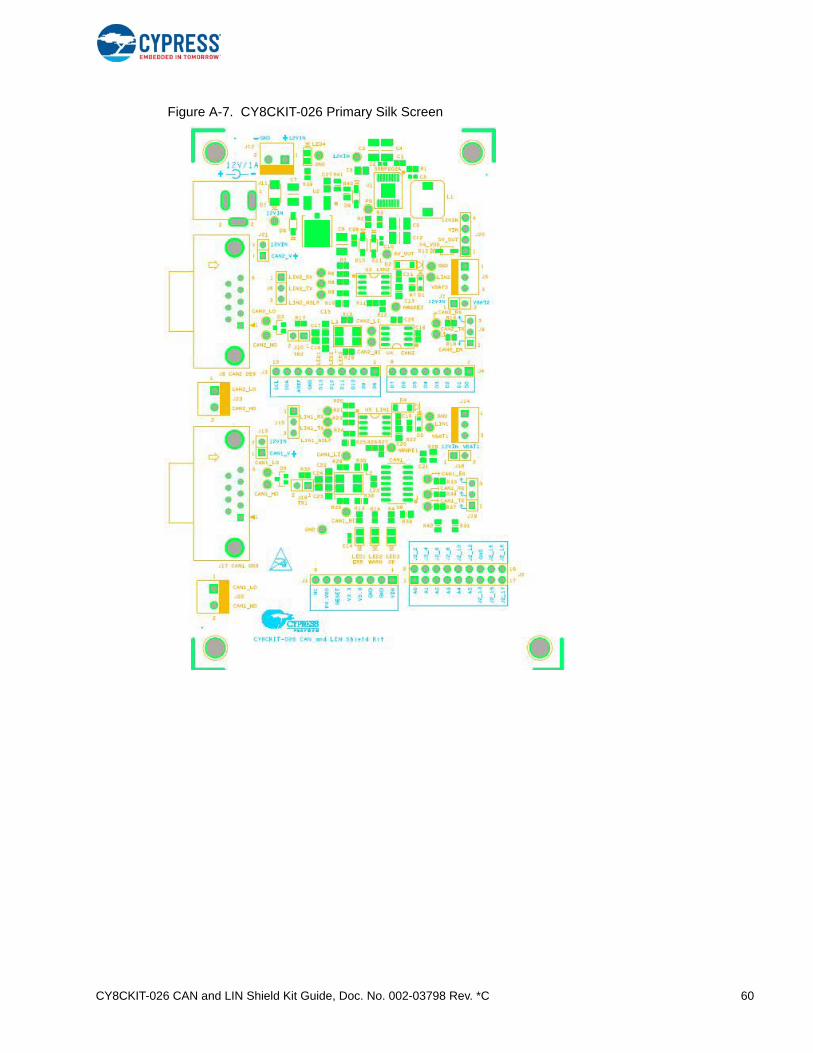
CY8CKIT-026 CAN and LIN Shield Kit Guide, Doc. No. 002-03798 Rev. *C 60
Figure A-7. CY8CKIT-026 Primary Silk Screen
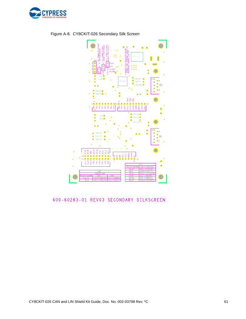
CY8CKIT-026 CAN and LIN Shield Kit Guide, Doc. No. 002-03798 Rev. *C 61
Figure A-8. CY8CKIT-026 Secondary Silk Screen
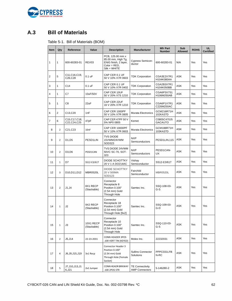
CY8CKIT-026 CAN and LIN Shield Kit Guide, Doc. No. 002-03798 Rev. *C 62
A.3 Bill of Materials
Table 5-1. Bill of Materials (BOM)
Item Qty Reference Value Description ManufacturerMfr Part Number
Sub Allowed
ROHSUL
Certified
1 1 600-60283-01 REV03
PCB, 125.00 mm x 85.00 mm, High Tg, ENIG finish, 2 layer, Color = RED, Silk = WHITE
Cypress Semicon-ductor
600-60283-01 N/A Yes Yes
2 5C11,C16,C19,C26,C28
0.1 uFCAP CER 0.1 UF 50 V 10% X7R 0603
TDK Corporation CGA3E2X7R1H104K080AA
ASK Yes Yes
3 1 C14 0.1 uFCAP CER 0.1 UF 50 V 10% X7R 0402
TDK CorporationCGA2B3X7R1H104K050BB
ASK Yes Yes
4 1 C7 10uF/50VCAP CER 10UF 50 V 20% X7S 1210
TDK CorporationCGA6P3X7S1H106M250AB
ASK Yes Yes
5 1 C8 22uFCAP CER 22UF 16 V 20% X7R 1210
TDK Corporation CGA6P1X7R1C226M250AC
ASK Yes Yes
6 2 C13,C20 1nFCAP CER 1000PF 50 V 10% X7R 0805
Murata ElectronicsGCM216R71H102KA37D
ASK Yes Yes
7 6C15,C17,C18,C22,C24,C25
47pFCAP CER 47PF 50 V 5% NP0 0805
KemetC0805C470J5GACAUTO
ASK Yes Yes
8 2 C21,C23 10nFCAP CER 10000PF 50 V 10% X7R 0603
Murata ElectronicsGCM188R71H103KA37D
ASK Yes Yes
9 2 D1,D5 PESD1LINTVS DIODE 15VWM/24VWM SOD323
NXP Semiconductors
PESD1LIN,115 ASK Yes Yes
10 2 D3,D6 PESD1CAN
TVS DIODE 24VWM 50VC SC-70, SOT-323
NXP Semiconductors
PESD1CAN-UX
ASK Yes Yes
11 1 D7 SS12‐E3/61TDIODE SCHOTTKY 20 V 1 A DO214AC
Vishay Semiconductor
SS12-E3/61T ASK Yes Yes
12 3 D10,D11,D12 MBR0520LDIODE SCHOTTKY 20 V 500MA SOD123
Fairchild Semiconductor
MBR0520L ASK Yes Yes
13 2 J1,J48X1 RECP (Stackable)
Connector Receptacle 8 Position 0.100" (2.54 mm) Gold Through Hole
Samtec Inc.SSQ-108-03-G-S
ASK Yes Yes
14 1 J29X2 RECP (Stackable)
Connector Receptacle 18 Position 0.100" (2.54 mm) Gold Through Hole [9x2]
Samtec Inc.SSQ-109-03-G-D
ASK Yes Yes
15 1 J310X1 RECP (Stackable)
Connector Receptacle 10 Position 0.100" (2.54 mm) Gold Through Hole
Samtec Inc.SSQ-110-03-G-S
ASK Yes Yes
16 2 J5,J14 22‐23‐2031CONN HEADER 3POS
.100 VERT TIN [KEYED]Molex Inc. 22232031 ASK Yes Yes
17 4 J6,J9,J15,J19 3x1 Recp
Connector Header 3
Position 0.100"
(2.54 mm) Gold
Through Hole [Female
Socket]
Sullins Connector Solutions
PPPC031LFBN-RC
ASK Yes Yes
18 5J7,J10,J13,J16,J21
2x1 JumperCONN HEADR BRKWAY
.100 2POS STR
TE Connectivity AMP Connectors
5-146280-2 ASK Yes Yes
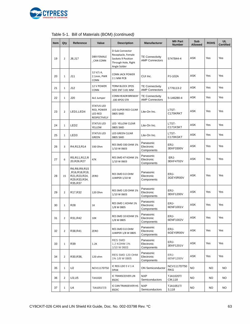
CY8CKIT-026 CAN and LIN Shield Kit Guide, Doc. No. 002-03798 Rev. *C 63
19 2 J8,J17DB9 FEMALE
_CAN CONN
D‐Sub Connector
Receptacle, Female
Sockets 9 Position
Through Hole, Right
Angle Solder
TE Connectivity AMP Connectors
5747844-4 ASK Yes Yes
20 1 J1112 V/1 A,
2.1mm, PWR
CONN
CONN JACK POWER
2.1 MM PCBCUI Inc. PJ-102A ASK Yes Yes
21 1 J1212 V POWER
CONN
TERM BLOCK 2POS
SIDE ENT 3.81 MM
TE Connectivity AMP Connectors
1776113-2 ASK Yes Yes
22 1 J20 4x1 JumperCONN HEADR BRKWAY
.100 4POS STR
TE Connectivity AMP Connectors
5-146280-4 ASK Yes Yes
23 2 LED1,LED4
STATUS LED
RED, POWER
LED RED
RESPECTIVELY
LED SUPER RED CLEAR
0805 SMDLite-On Inc.
LTST-C170KRKT
ASK Yes Yes
24 1 LED2STATUS LED
YELLOW
LED YELLOW CLEAR
0805 SMDLite-On Inc.
LTST-C171KSKT
ASK Yes Yes
25 1 LED3STATUS LED
GREEN
LED GREEN CLEAR
0805 SMDLite-On Inc.
LTST-C170KGKT
ASK Yes Yes
26 3 R4,R13,R14 330 OhmRES SMD 330 OHM 1%
1/10 W 0603
Panasonic Electronic Components
ERJ-3EKF3300V
ASK Yes Yes
27 6R5,R11,R12,R20,R26,R27
47KRES SMD 47 KOHM 1%
1/10 W 0603
Panasonic Electronic Components
ERJ-3EKF4702V
ASK Yes Yes
28 15
R6,R8,R9,R15,R16,R18,R19,R21,R23,R24,R29,R33,R34,R35,R37
ZERORES SMD 0.0 OHM
JUMPER 1/10 W
Panasonic Electronic Components
ERJ-3GEY0R00V
ASK Yes Yes
29 2 R17,R32 120 OhmRES SMD 120 OHM 1%
1/10 W 0603
Panasonic Electronic Components
ERJ-3EKF1200V
ASK Yes Yes
30 1 R28 1KRES SMD 1 KOHM 1%
1/8 W 0805
Panasonic Electronic Components
ERJ-6ENF1001V
ASK Yes Yes
31 2 R31,R42 10KRES SMD 10 KOHM 1%
1/8 W 0805
Panasonic Electronic Components
ERJ-6ENF1002V
ASK Yes Yes
32 2 R38,R41 ZERORES SMD 0.0 OHM
JUMPER 1/8 W 0805
Panasonic Electronic Components
ERJ-6GEY0R00V
ASK Yes Yes
33 1 R39 1.2K
RES SMD 1.2 KOHM 1% 1/10 W 0603
Panasonic Electronic Components
ERJ-3EKF1201V
ASK Yes Yes
34 2 R30,R36, 120 ohmRES SMD 120 OHM 1% 1/8 W 0805
Panasonic Electronic Components
ERJ-6ENF1200V
ASK Yes Yes
35 1 U2 NCV1117DT50IC REG LDO 5 V 1 A
DPAKON Semiconductor
NCV1117DT50RKG
NO NO NO
36 2 U3,U5 TJA1020IC TRANSCEIVER LIN
8SOIC
NXP Semiconductors
TJA1020T/CM,118
NO NO NO
37 1 U4 TJA1051T/3IC CAN TRANSEIVER HS
8SOIC
NXP Semiconductors
TJA1051T/3,118
NO NO NO
Table 5-1. Bill of Materials (BOM) (continued)
Item Qty Reference Value Description ManufacturerMfr Part Number
Sub Allowed
ROHSUL
Certified
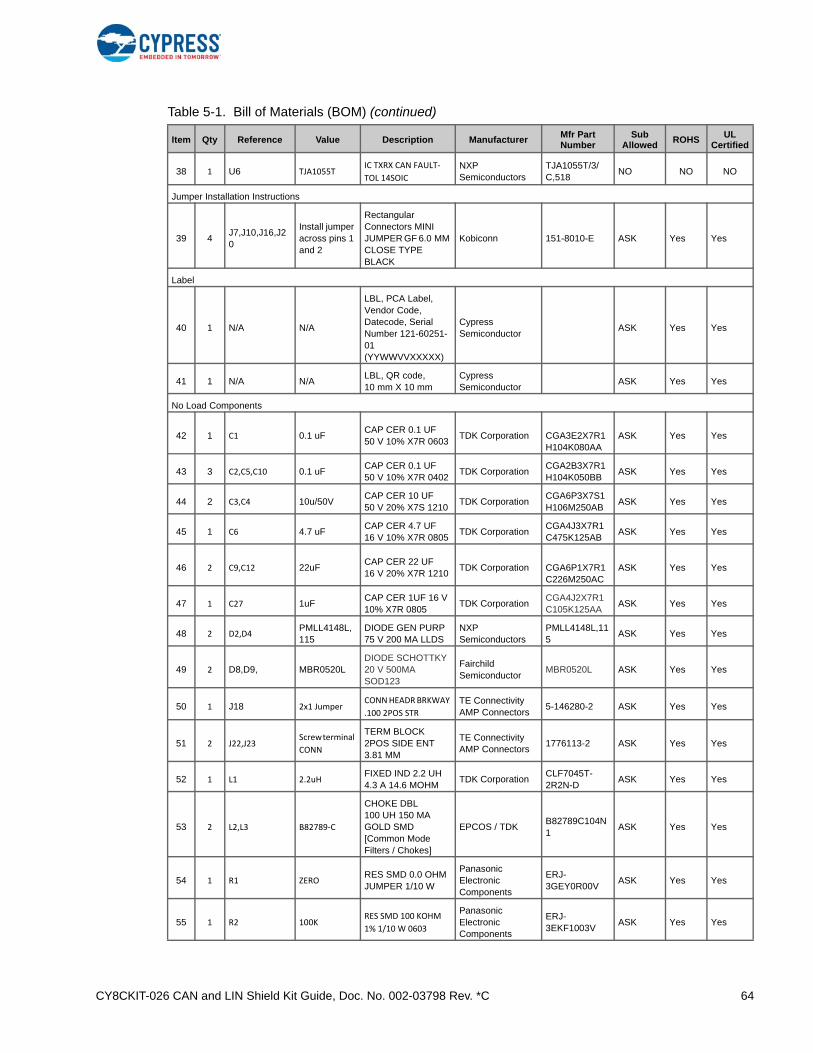
CY8CKIT-026 CAN and LIN Shield Kit Guide, Doc. No. 002-03798 Rev. *C 64
38 1 U6 TJA1055TIC TXRX CAN FAULT‐
TOL 14SOIC
NXP Semiconductors
TJA1055T/3/C,518
NO NO NO
Jumper Installation Instructions
39 4J7,J10,J16,J20
Install jumper across pins 1 and 2
Rectangular Connectors MINI JUMPER GF 6.0 MM CLOSE TYPE BLACK
Kobiconn 151-8010-E ASK Yes Yes
Label
40 1 N/A N/A
LBL, PCA Label, Vendor Code, Datecode, Serial Number 121-60251-01 (YYWWVVXXXXX)
Cypress Semiconductor
ASK Yes Yes
41 1 N/A N/ALBL, QR code, 10 mm X 10 mm
Cypress Semiconductor
ASK Yes Yes
No Load Components
42 1 C1 0.1 uFCAP CER 0.1 UF 50 V 10% X7R 0603
TDK Corporation CGA3E2X7R1H104K080AA
ASK Yes Yes
43 3 C2,C5,C10 0.1 uFCAP CER 0.1 UF 50 V 10% X7R 0402
TDK CorporationCGA2B3X7R1H104K050BB
ASK Yes Yes
44 2 C3,C4 10u/50VCAP CER 10 UF 50 V 20% X7S 1210
TDK CorporationCGA6P3X7S1H106M250AB
ASK Yes Yes
45 1 C6 4.7 uFCAP CER 4.7 UF 16 V 10% X7R 0805
TDK CorporationCGA4J3X7R1C475K125AB
ASK Yes Yes
46 2 C9,C12 22uFCAP CER 22 UF 16 V 20% X7R 1210
TDK Corporation CGA6P1X7R1C226M250AC
ASK Yes Yes
47 1 C27 1uFCAP CER 1UF 16 V 10% X7R 0805
TDK CorporationCGA4J2X7R1C105K125AA
ASK Yes Yes
48 2 D2,D4PMLL4148L,115
DIODE GEN PURP 75 V 200 MA LLDS
NXP Semiconductors
PMLL4148L,115
ASK Yes Yes
49 2 D8,D9, MBR0520LDIODE SCHOTTKY 20 V 500MA SOD123
Fairchild Semiconductor
MBR0520L ASK Yes Yes
50 1 J18 2x1 JumperCONN HEADR BRKWAY
.100 2POS STR
TE Connectivity AMP Connectors
5-146280-2 ASK Yes Yes
51 2 J22,J23Screw terminal
CONN
TERM BLOCK 2POS SIDE ENT 3.81 MM
TE Connectivity AMP Connectors
1776113-2 ASK Yes Yes
52 1 L1 2.2uHFIXED IND 2.2 UH 4.3 A 14.6 MOHM
TDK CorporationCLF7045T-2R2N-D
ASK Yes Yes
53 2 L2,L3 B82789‐C
CHOKE DBL 100 UH 150 MA GOLD SMD [Common Mode Filters / Chokes]
EPCOS / TDKB82789C104N1
ASK Yes Yes
54 1 R1 ZERORES SMD 0.0 OHM JUMPER 1/10 W
Panasonic Electronic Components
ERJ-3GEY0R00V
ASK Yes Yes
55 1 R2 100KRES SMD 100 KOHM
1% 1/10 W 0603
Panasonic Electronic Components
ERJ-3EKF1003V
ASK Yes Yes
Table 5-1. Bill of Materials (BOM) (continued)
Item Qty Reference Value Description ManufacturerMfr Part Number
Sub Allowed
ROHSUL
Certified
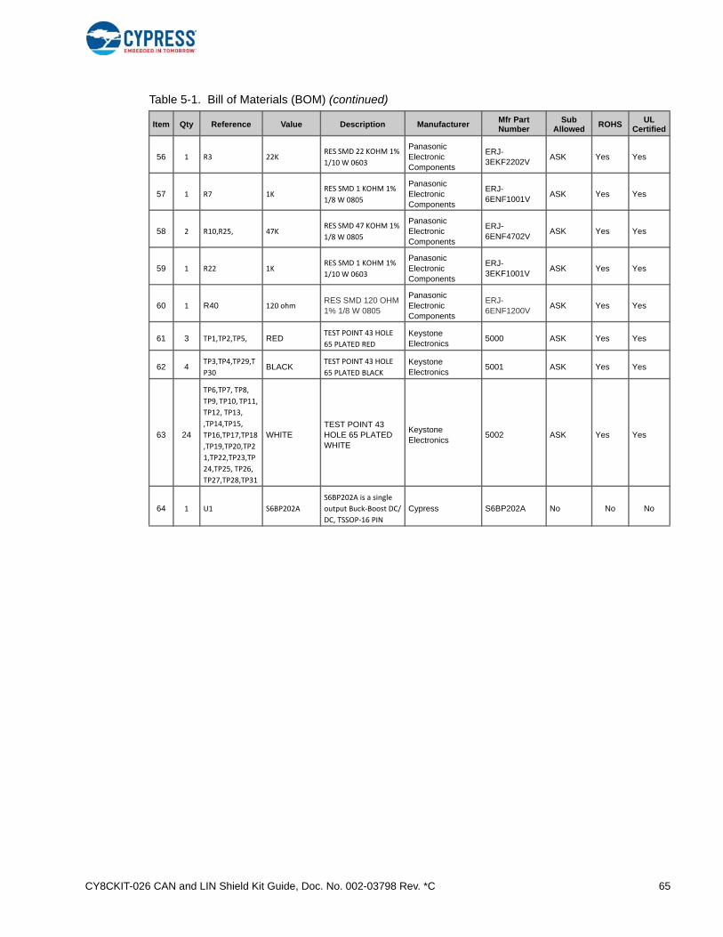
CY8CKIT-026 CAN and LIN Shield Kit Guide, Doc. No. 002-03798 Rev. *C 65
56 1 R3 22KRES SMD 22 KOHM 1%
1/10 W 0603
Panasonic Electronic Components
ERJ-3EKF2202V
ASK Yes Yes
57 1 R7 1KRES SMD 1 KOHM 1%
1/8 W 0805
Panasonic Electronic Components
ERJ-6ENF1001V
ASK Yes Yes
58 2 R10,R25, 47KRES SMD 47 KOHM 1%
1/8 W 0805
Panasonic Electronic Components
ERJ-6ENF4702V
ASK Yes Yes
59 1 R22 1KRES SMD 1 KOHM 1%
1/10 W 0603
Panasonic Electronic Components
ERJ-3EKF1001V
ASK Yes Yes
60 1 R40 120 ohmRES SMD 120 OHM 1% 1/8 W 0805
Panasonic Electronic Components
ERJ-6ENF1200V
ASK Yes Yes
61 3 TP1,TP2,TP5, REDTEST POINT 43 HOLE
65 PLATED RED
Keystone Electronics
5000 ASK Yes Yes
62 4TP3,TP4,TP29,T
P30BLACK
TEST POINT 43 HOLE
65 PLATED BLACK
Keystone Electronics
5001 ASK Yes Yes
63 24
TP6,TP7, TP8,
TP9, TP10, TP11,
TP12, TP13,
,TP14,TP15,
TP16,TP17,TP18
,TP19,TP20,TP2
1,TP22,TP23,TP
24,TP25, TP26,
TP27,TP28,TP31
WHITETEST POINT 43 HOLE 65 PLATED WHITE
Keystone Electronics
5002 ASK Yes Yes
64 1 U1 S6BP202A
S6BP202A is a single
output Buck‐Boost DC/
DC, TSSOP‐16 PIN
Cypress S6BP202A No No No
Table 5-1. Bill of Materials (BOM) (continued)
Item Qty Reference Value Description ManufacturerMfr Part Number
Sub Allowed
ROHSUL
Certified
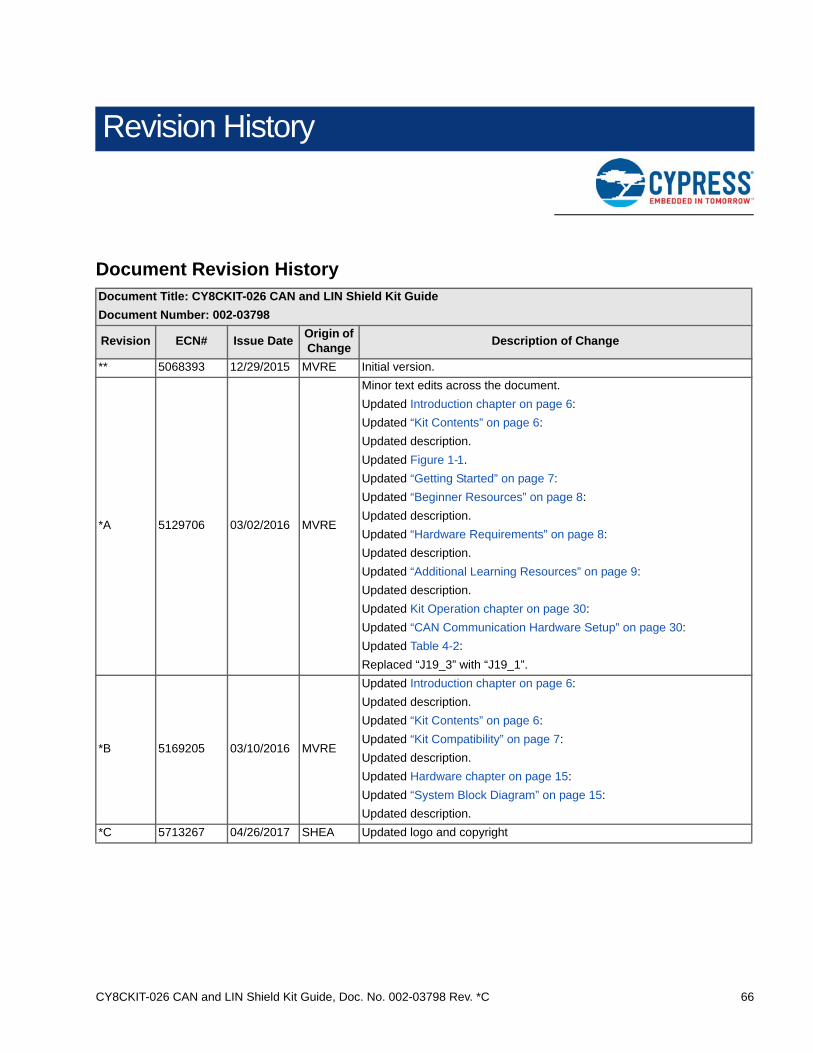
CY8CKIT-026 CAN and LIN Shield Kit Guide, Doc. No. 002-03798 Rev. *C 66
Revision History
Document Revision HistoryDocument Title: CY8CKIT-026 CAN and LIN Shield Kit Guide
Document Number: 002-03798
Revision ECN# Issue DateOrigin of Change
Description of Change
** 5068393 12/29/2015 MVRE Initial version.
*A 5129706 03/02/2016 MVRE
Minor text edits across the document.
Updated Introduction chapter on page 6:
Updated “Kit Contents” on page 6:
Updated description.
Updated Figure 1-1.
Updated “Getting Started” on page 7:
Updated “Beginner Resources” on page 8:
Updated description.
Updated “Hardware Requirements” on page 8:
Updated description.
Updated “Additional Learning Resources” on page 9:
Updated description.
Updated Kit Operation chapter on page 30:
Updated “CAN Communication Hardware Setup” on page 30:
Updated Table 4-2:
Replaced “J19_3” with “J19_1”.
*B 5169205 03/10/2016 MVRE
Updated Introduction chapter on page 6:
Updated description.
Updated “Kit Contents” on page 6:
Updated “Kit Compatibility” on page 7:
Updated description.
Updated Hardware chapter on page 15:
Updated “System Block Diagram” on page 15:
Updated description.
*C 5713267 04/26/2017 SHEA Updated logo and copyright


