Embed Size (px)
Citation preview
Bachelor Project
CzechTechnicalUniversityin Prague
F3 Faculty of Electrical EngineeringDepartment of Measurement
LIN Slave Simulator
Aleksandra Pereverzeva
Supervisor: doc. Ing. Jiří Novák, Ph.D.Field of study: Open InformaticsSubfield: Computer SystemsMay 2018

ii

Acknowledgements
I would like to thank my supervisor doc.Ing. Jiří Novák, Ph.D. for guidance, ad-vices and passed knowledge.
Declaration
Prohlašuji, že jsem předloženou prácivypracovala samostatně pod dohledem ve-doucího, a že jsem uvedla veškerou použi-tou literaturu.
V Praze, 25. May 2018
iii
Abstract
This bachelor’s thesis describes the pro-cess of designing and realization of a hard-ware module, which will be used mostlyin automotive industry. The function ofthe module is simulation of several LINslaves depending on orders and informa-tion received through CAN bus. Thenthe process of implementation of softwarefollows. The module consists of a proces-sor, LIN, CAN and SWD interfaces. Thegoal of this thesis is implementation ofa working module, which will be able tosend data to LIN bus and then change thisdata on request from CAN bus. The firstpart of the document focuses on the the-oretical knowledge needed to implementand understand the module, such as usedtechnologies. The second part deals withthe description of the module itself, usedcomponents, connection of the circuits,PCB layers, the explanation of the codeparts and its algorithm. The outcome ofthe work is the design, the module and theprogram for configuration of the module.
Keywords: LIN, CAN, module, PCB
Supervisor: doc. Ing. Jiří Novák, Ph.D.Technická 2,166 27Praha 6
Abstrakt
Tato bakalářská práce popisuje návrh aproces realizace hardwarového modulu,který se bude používat převážně v auto-mobilovém průmyslu. Hlavní funkcí mo-dulu je simulace několika LIN slavů nazákladě přijatých požadavků od sběrniceCAN. Dále je popsán postup implemen-tace softwaru. Modul se skládá z proce-soru, rozhraní LIN, CAN a SWD. Cílemtéto práce je implementace funkčního mo-dulu, který by byl schopný odesílat datana sběrnici LIN a pak tato data měnitpodle požadavku ze sběrnice CAN. Prvníčást této práce se zabývá teoretickými zna-lostmi, které jsou potřeba vědět při im-plementaci modulu a pro pochopení jehofungování, jako například použité techno-logie. Druhá část se soustředí na popissamotného modulu, použitých součástek,zapojení obvodů, vrstev desky plošnýchspojů a vysvětlení částí kódu a algoritmů.Výsledkem práce je návrh, samotný modula programové vybavení pro jeho konfigu-raci.
Klíčová slova: LIN, CAN, modul, DPS
Překlad názvu: Simulátor LIN Slave
iv
Contents
1 Introduction 1
1.1 Used Abbreviations . . . . . . . . . . . . 2
Part ITheoretical part
2 Introduction 5
3 Used Technologies: Networks 7
3.1 Media Access Control . . . . . . . . . . 7
3.2 CAN . . . . . . . . . . . . . . . . . . . . . . . . . 8
3.2.1 General information . . . . . . . . . 8
3.2.2 History . . . . . . . . . . . . . . . . . . . . 8
3.2.3 Communication protocols . . . . 9
3.2.4 Implementation . . . . . . . . . . . . . 9
3.2.5 Communication on the bus . . 10
3.3 Error detection . . . . . . . . . . . . . . . 11
3.4 LIN . . . . . . . . . . . . . . . . . . . . . . . . . 11
3.4.1 General information . . . . . . . . 11
3.4.2 History . . . . . . . . . . . . . . . . . . . 13
3.4.3 Communication on the bus . . 14
3.4.4 LIN frames . . . . . . . . . . . . . . . . 14
3.4.5 Header of the frame . . . . . . . . 17
3.4.6 Response . . . . . . . . . . . . . . . . . 17
3.5 UART. . . . . . . . . . . . . . . . . . . . . . . 18
3.5.1 General information . . . . . . . . 18
3.5.2 Types of UART. . . . . . . . . . . . 18
3.5.3 Communication . . . . . . . . . . . . 19
3.6 JTAG . . . . . . . . . . . . . . . . . . . . . . . 19
3.7 SWD. . . . . . . . . . . . . . . . . . . . . . . . 20
4 Used Technologies: Circuits,Components and Devices 21
4.1 Power supply . . . . . . . . . . . . . . . . . 21
4.1.1 Linear regulators . . . . . . . . . . . 21
4.1.2 Switched-mode power supply 22
4.1.3 Step-down converters . . . . . . . 22
4.2 Types of components andpackages . . . . . . . . . . . . . . . . . . . . . . . 23
4.2.1 Quad Flat Package . . . . . . . . . 23
v
4.2.2 Dual in-line package . . . . . . . . 23
4.2.3 Ball Grid Array . . . . . . . . . . . . 24
4.3 LED connection . . . . . . . . . . . . . . 24
Part IIPractical part
5 Design of the module 27
5.1 Introduction . . . . . . . . . . . . . . . . . 27
5.1.1 Hardware Requirements . . . . 27
5.1.2 Proposal of the solution . . . . . 28
5.1.3 Bypass Capacitors . . . . . . . . . 28
5.1.4 Scheme and Components . . . . 28
5.2 The Processor . . . . . . . . . . . . . . . . 30
5.3 Power converter . . . . . . . . . . . . . . 31
5.4 CAN transceiver . . . . . . . . . . . . . . 31
5.5 LIN UART converter . . . . . . . . . . 32
5.6 SWD. . . . . . . . . . . . . . . . . . . . . . . . 33
5.7 LEDs . . . . . . . . . . . . . . . . . . . . . . . 33
6 Program 35
7 Conclusion 41
Appendices
A Bibliography 51
B Project Specification 54
vi
Chapter 1
Introduction
Nowadays we can observe, that engineers of automotive industry replacemechanical elements with much more intelligent mechatronic components andsystems, which need a way to communicate with each other. This is wherenetworks that are relying on wires come in handy. Usually, they are relativelycheap and fast and sometimes even more reliable than mechanical types ofdata transferring which makes them even more useful. But what if thesewires with data, so-called buses, of different types should send some orders toeach other? It seems that additional device would be necessary, a device thatcan access both networks in some way and influence communication on onebus with orders received from the other bus.
This project is focused on the design of such a device and then its furtherconfiguration. The main requirements are the provision of a possibility of theconfiguration of communication frames on LIN bus via CAN bus, supportof transmission of Event-driven frames. It might be vital in case of testingthe networks or some of the nodes of the LIN bus break down but theircontribution into communication on the LIN bus is needed. As I have alreadymentioned, this device can be used in automotive industry, such as ŠkodaAuto for example. Similar devices exist, such as [Emu], but their prices startat $355 (7277 CZK) according to [Phy], so there is also a secondary goal tolower this price.
1
1. Introduction .....................................1.1 Used Abbreviations
. CAN – Controller Area Network. LIN – Local Interconnect Network. U(S)ART – Universal (Synchronous) Asynchronous Receiver and Trans-mitter.MCU – Microcontroller Unit. JTAG - Joint Test Action Group. ASICS – Application-specific integrated circuit. CRC - Cyclic redundancy check. PCB – Printed Circuit Board. L – Electric Induction. I – Electric Current. V – Electric Voltage. SMT – Surface Mount Technology. TVS - Transient-voltage-suppression diode. SWD - Serial Wire Debug. IDE - Integrated Development Environment
2

3

1. Introduction .....................................
Part I
Theoretical part
4
Chapter 2
Introduction
This part is dedicated to the description of technologies used for fulfilling thisproject.
The first chapter will focus on the network technologies such as CAN andLIN. This part will contain communication examples of these networks andalso general information about UART technology.
The second chapter consists of more abstract conception about powersupply, components and LED connections.
This part tempts to achieve the following goal: giving the reader all theneeded theoretical knowledge for understanding of the structure of the module,its necessary components and its behavior.
5

6
Chapter 3
Used Technologies: Networks
3.1 Media Access Control
Media Access Control (MAC) is a sublayer of a Data Link Layer of the OSIReference Model. Its protocols also describe the process of controlling theway devices can access the shared network. The nature of MAC can bedeterministic and non-deterministic [sCN] [Med]...1. Deterministic Access
A convention that garantees all stations the right to communicate withina certain time frame according to the priorities assigned by the adminis-trator of the system. In this type of MAC, the collisions are not possible,because all of the communication is centralized...a. Master-Slave
A special node called Master inquires, so called, Slave nodes. Slavenodes can only send responses, they are not allowed to initiate thecommunication. This type of communication is easy to implementand price for this is a limited number of devices and high dependencyon Master node...b. TDMA (Time Division Multiple Access) - strictly given time slots,during which devices are allowed to send information to the network...2. Non-deterministic Access
7
3. Used Technologies: Networks................................a. ALOHA - one of the oldest protocol. If a station has somethingto sends, it starts transmitting; if while transmitting it receivedanother message, a collision has occurred and all stations have toresend the data...b. CSMA (Carrier Sense Multiple Access) - Equivalent nodes have towait for media to be free for starting the transmission. Collisionscan occur, but are not necessarily detected.(i) CSMA/CD (Collision Detection) - all collisions are detected.
After the collision nodes wait a random period of time Ta · dto start transmission again, where Ta is a constant and d is arandom number.
(ii) CSMA/CA ( Collision Avoidance) - collision may not be de-tected. After a detection of a free media, a station waits for arandom period of time and after that starts transmission. Thistype is used in wireless networks.
(iii) CSMA/CR (Collision Resolution) - if a collision was detected,a frame with the highest priority is sent, all other stations haveto repeat the transmission. This type of media access is usedfor CAN bus.
3.2 CAN
3.2.1 General information
CAN is a type of a bus that is usually used in automotive industry for commu-nication between microcontrollers and devices inside a vehicle without a hostcomputer. It is a message based protocol designed for automotive applicationsbut nowadays it is used in several industry branches such as industrial automa-tion and medical equipment. It is so widely spread thanks to independence tomedia and extremely high reliability even in worst environmental conditions.
3.2.2 History
The bus was invented by the company Robert Bosch GmbH and was presentedin 1986; first CAN controller was introduced one year later by Intel and Philips.In 1988 CAN bus was used for the first time (in BMW automobiles of series8) [CAN].
8
........................................ 3.2. CAN
3.2.3 Communication protocols
The bus has two wires CANH (high) and CANL (low). Theoretical trans-mission speed is 1.5 Mb/s; however, two physical layer variants provide themaximum speed of 1Mb/s and 125Mb/s respectively. While the bus is notactive it exists in the idle or recessive state. In the recessive state of higherspeed signals are 2.5 V for both CANH and CANL; for the dominant stateof higher speed, CANH has the voltage of 3.5 V, while CANL has 1.5 Vaccording to ISO 11898 [ISOb]. Thanks to this the differential pair of 2 V iscreated.
Another ISO 11519 [ISOa] shows that for lower speed CANH conducts1.75 V in recessive and 4 V in the dominant state, for CANL these valuesare 3.25 V and 4 V respectively. Unlike high speed, Low-speed standard doesnot require the resistors of 120 Ohm at the end of the linear bus because atthis speed signal reflections are not originated. CAN bus can be taken asa compilation of two standards: Standard CAN (version 2.0A), which uses11-bit identification, and Extended CAN (version 2.0B), which uses 29-bitidentification [Zhu10].
There is another CAN protocol called CAN FD (Flex Data-Rate). CAN FDhas a different frame structure, which allows larger data flow and a possibilityto turn higher bit rate. CAN FD is created in such a way that it can co-existon the bus with controllers of older standards [Bos12].
3.2.4 Implementation
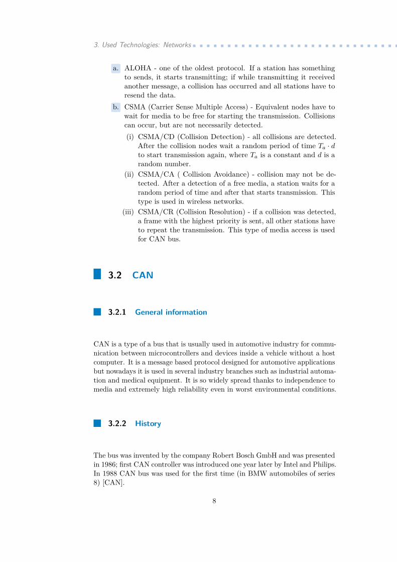
The implementation requires 120Ohm resistors on both ends of the bus toprevent signal reflection, in other words for impedance matching (can beseen on [3.1]). The value of 120 Ohm corresponds to the line impedanceof usually used twisted pair cables. In an ideal situation the number ofconnected terminals is not limited, but in order to save useful dynamic andstatic properties, it is recommended to put these limits, for example on 30terminals [HMS02].
9
3. Used Technologies: Networks..............................
Figure 3.1: Diagram of the CAN bus network [HMS02].
3.2.5 Communication on the bus
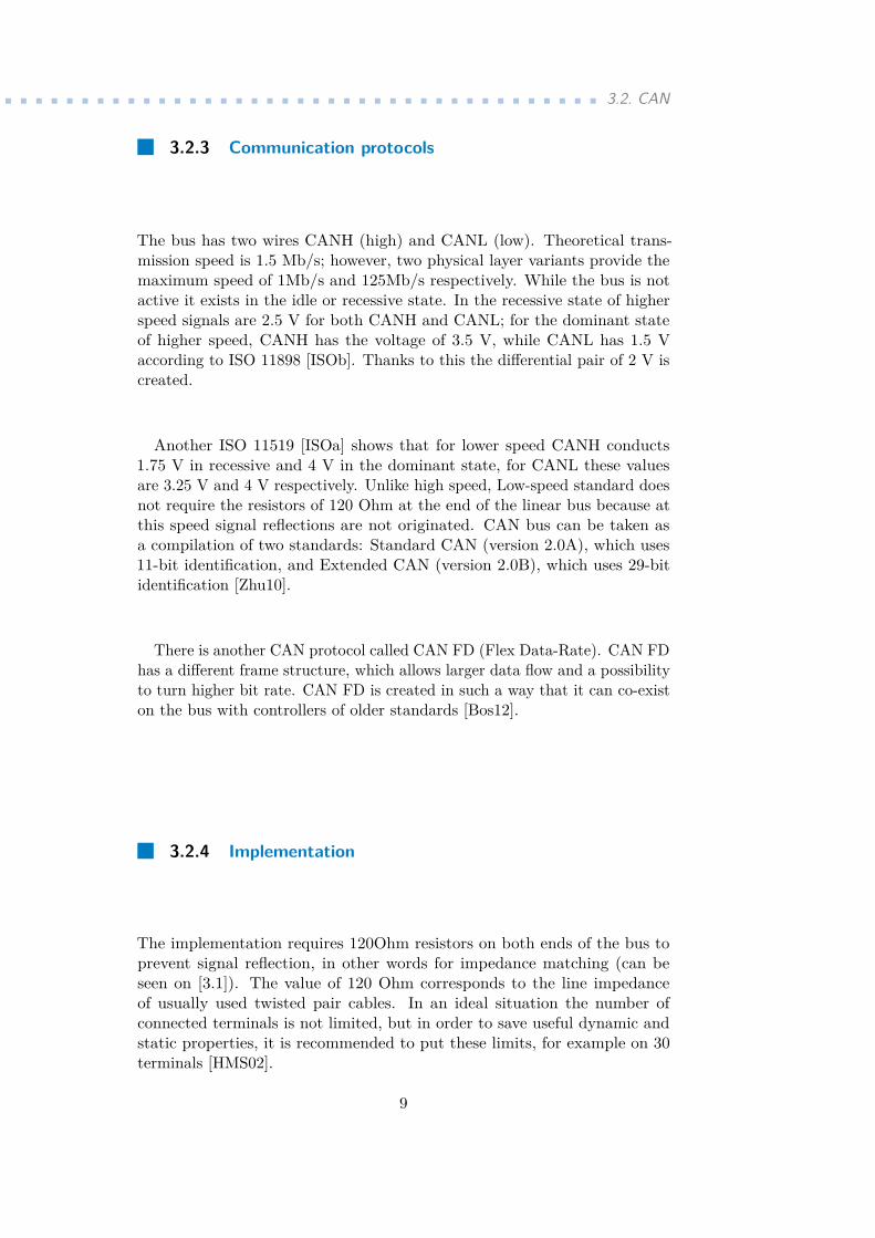
In CAN 2.0 messages can be divided into 4 types, the first couple of themis for transmitting and receiving the messages and the second couple is formanagement of the network. The messages are received by every node thatis connected to the bus and is in receive mode. Every message contains anidentifier, which shows the content of the message and then is used by theterminals to decide whether the message is determined for this node andshould be evaluated or not and should be destroyed. This mechanism is calledfiltration.
CAN bus uses protocol CSMA/CR for media access. This means that incase a collision takes place when two or more messages are sent at the sametime, their priorities are evaluated and only the message with higher priorityis sent first.
Existing frames: Data frame, Remote frame (request for data), Error frame,Overload frame. An example of a base frame can be seen on [3.2]
Figure 3.2: Structure of a CAN bus frame [htt].
10
....................................3.3. Error detection
3.3 Error detection
For error detection it is possible to use one or several of the following mostcommon methods:..1. Monitoring..2. Bit stuffing..3. CRC
Monitoring is a mechanism of an error detection in which the transmitteralways compares the data sent and the data on the bus.
Bit stuffing is a mechanism that inserts into the message in the transmitternode an additional bit after every 5 same bits in a row. When the receiverfinds out that this bit is missing, it generates an error message.
Another controlling mechanism is the generation of CRC code. CRCcode is a sequence of values which is generated in a certain way, then addedto the message. The receiver after that generates the CRC code of his ownand compares it to the one in the message if they differ, an error message isgenerated[Whab].
3.4 LIN
3.4.1 General information
LIN is a serial network protocol that is used for intercommunication amongseveral components in a vehicle. Appeared as a cheaper but slower substitutionof the CAN bus. LIN over DC powerline is standardized as ISO/AWI 17987-8[ISOe]. LIN supports remote application within a car’s network. This bus isan asynchronous bus that uses unbalanced communication among the nodes.The main features are:
11
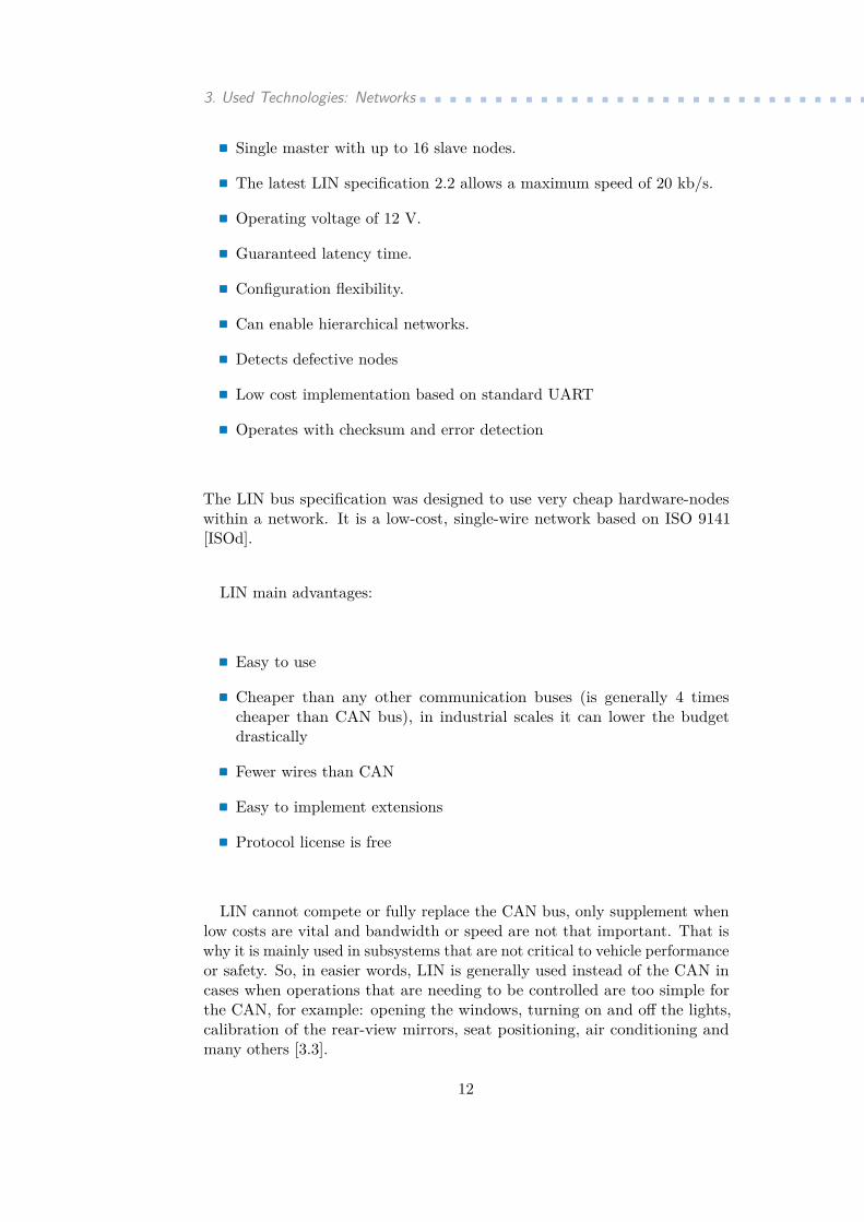
3. Used Technologies: Networks............................... Single master with up to 16 slave nodes.. The latest LIN specification 2.2 allows a maximum speed of 20 kb/s..Operating voltage of 12 V..Guaranteed latency time.. Configuration flexibility.. Can enable hierarchical networks.. Detects defective nodes. Low cost implementation based on standard UART.Operates with checksum and error detection
The LIN bus specification was designed to use very cheap hardware-nodeswithin a network. It is a low-cost, single-wire network based on ISO 9141[ISOd].
LIN main advantages:
. Easy to use. Cheaper than any other communication buses (is generally 4 timescheaper than CAN bus), in industrial scales it can lower the budgetdrastically. Fewer wires than CAN. Easy to implement extensions. Protocol license is free
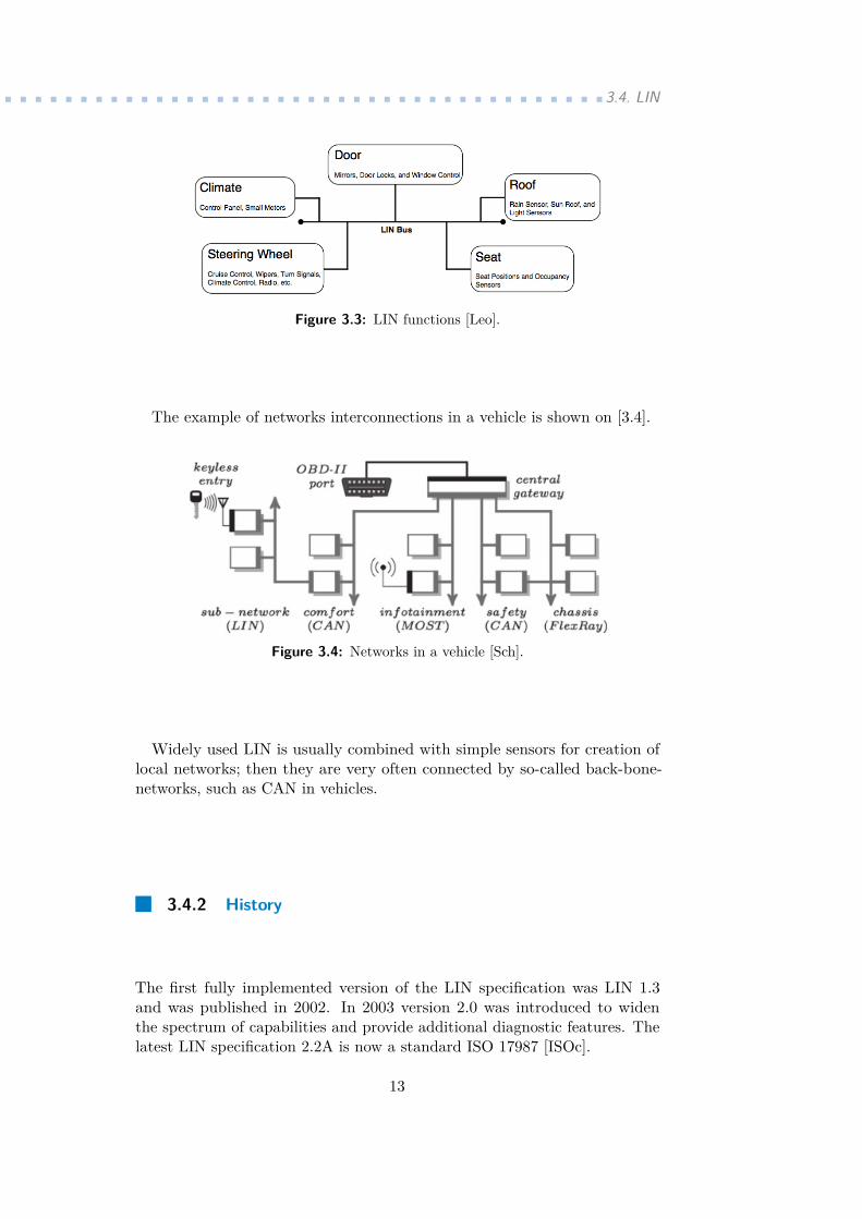
LIN cannot compete or fully replace the CAN bus, only supplement whenlow costs are vital and bandwidth or speed are not that important. That iswhy it is mainly used in subsystems that are not critical to vehicle performanceor safety. So, in easier words, LIN is generally used instead of the CAN incases when operations that are needing to be controlled are too simple forthe CAN, for example: opening the windows, turning on and off the lights,calibration of the rear-view mirrors, seat positioning, air conditioning andmany others [3.3].
12
.........................................3.4. LIN
Figure 3.3: LIN functions [Leo].
The example of networks interconnections in a vehicle is shown on [3.4].
Figure 3.4: Networks in a vehicle [Sch].
Widely used LIN is usually combined with simple sensors for creation oflocal networks; then they are very often connected by so-called back-bone-networks, such as CAN in vehicles.
3.4.2 History
The first fully implemented version of the LIN specification was LIN 1.3and was published in 2002. In 2003 version 2.0 was introduced to widenthe spectrum of capabilities and provide additional diagnostic features. Thelatest LIN specification 2.2A is now a standard ISO 17987 [ISOc].
13
3. Used Technologies: Networks..............................3.4.3 Communication on the bus
The bus has three modes: slow, medium and fast. The realization of the LINnode is relatively simple; besides it does not require a crystal oscillator, anRC oscillator is enough, that can reduce the price [DEK+01].
All communication is initiated by the master. Due to this fact, collisiondetection mechanism is not necessary. Only one slave can reply to the givenmessage because at the beginning of the frame there is always an identifier ofthe message, which eventually determines to which slave node this message isintended. Master can reply to its own messages. For the baud-rate stabilitywithin one frame there is a special SYNC field in the header of the frame [12].
The role of slaves and a master are normally performed by microcontrollerswith UART capability. But in some cases, when low cost, little space, andlow power are extremely important, it can be implemented in specializedhardware or ASICs [Mos08].
3.4.4 LIN frames
Content of the frames is the following:..1. Synchronization break..2. Synchronization byte..3. Identifier byte..4. Data bytes..5. Checksum byte
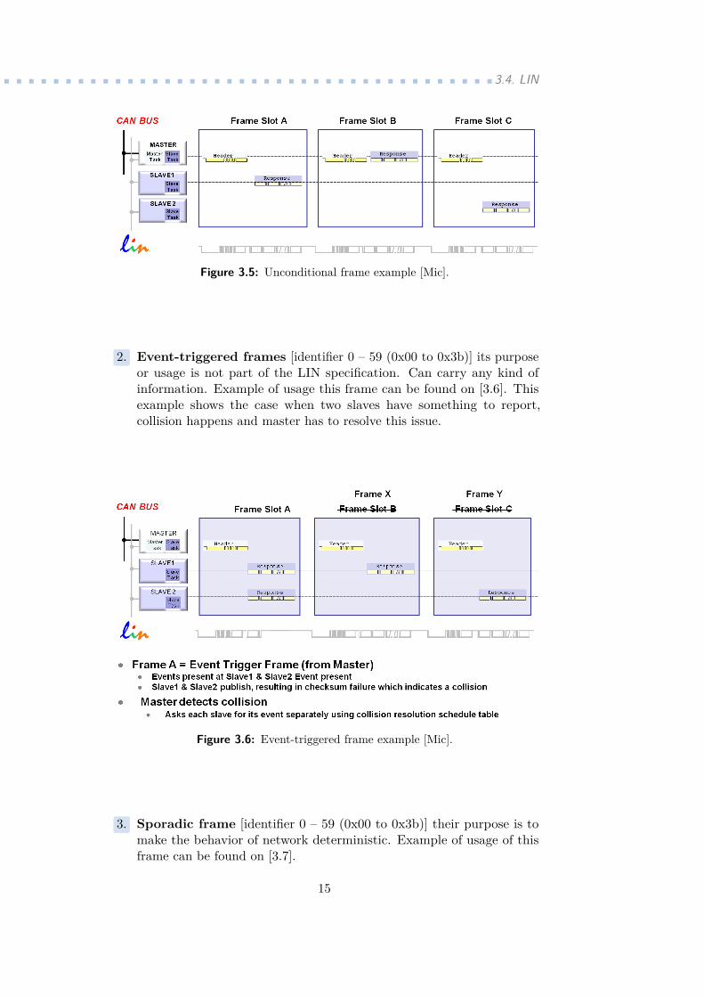
Types of frames:..1. Unconditional frames [identifier 0 – 59 (0x00 to 0x3b)] carry signalsto all the subscribers. If no errors are found, they can be made availableto the application. Example of usage of this frame can be found on [3.5].
14
.........................................3.4. LIN
Figure 3.5: Unconditional frame example [Mic].
..2. Event-triggered frames [identifier 0 – 59 (0x00 to 0x3b)] its purposeor usage is not part of the LIN specification. Can carry any kind ofinformation. Example of usage this frame can be found on [3.6]. Thisexample shows the case when two slaves have something to report,collision happens and master has to resolve this issue.
Figure 3.6: Event-triggered frame example [Mic].
..3. Sporadic frame [identifier 0 – 59 (0x00 to 0x3b)] their purpose is tomake the behavior of network deterministic. Example of usage of thisframe can be found on [3.7].
15
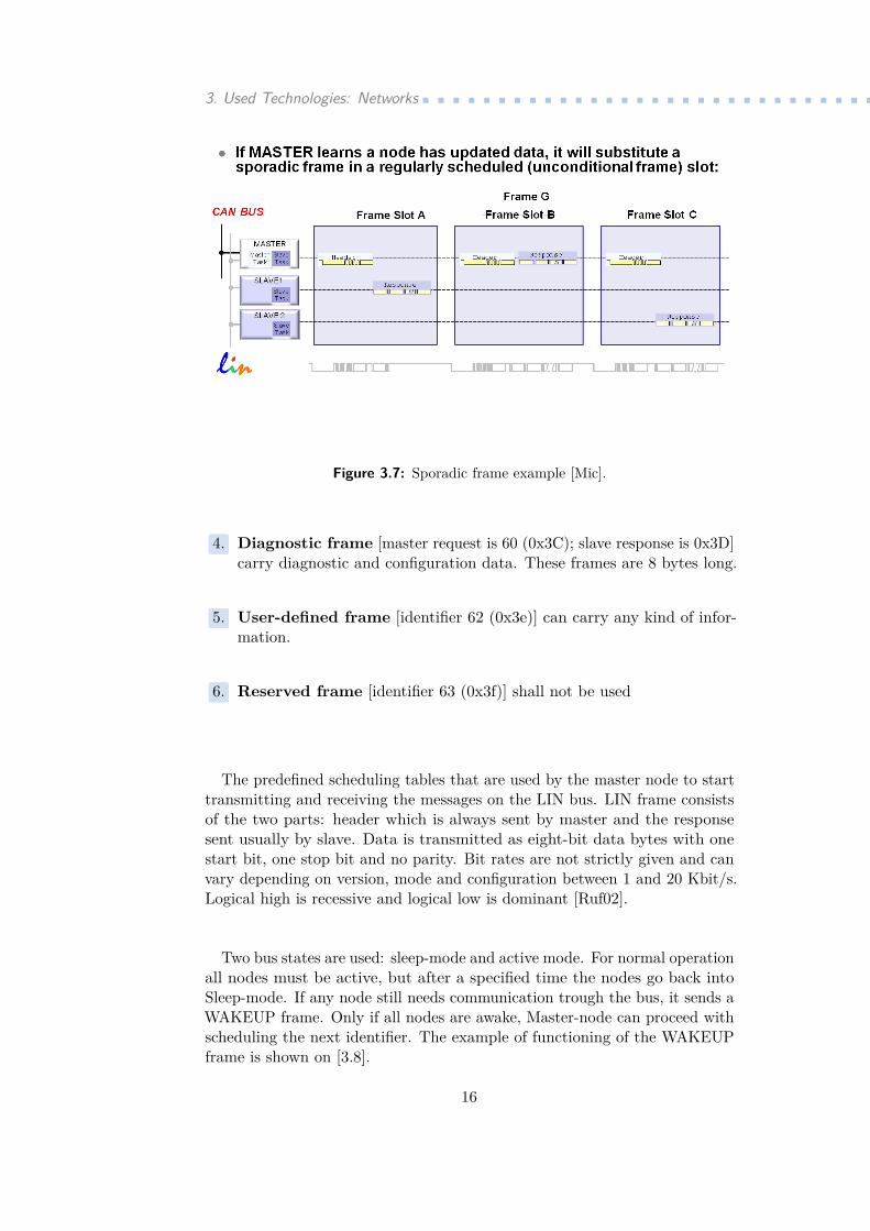
3. Used Technologies: Networks..............................
Figure 3.7: Sporadic frame example [Mic]...4. Diagnostic frame [master request is 60 (0x3C); slave response is 0x3D]carry diagnostic and configuration data. These frames are 8 bytes long...5. User-defined frame [identifier 62 (0x3e)] can carry any kind of infor-mation...6. Reserved frame [identifier 63 (0x3f)] shall not be used
The predefined scheduling tables that are used by the master node to starttransmitting and receiving the messages on the LIN bus. LIN frame consistsof the two parts: header which is always sent by master and the responsesent usually by slave. Data is transmitted as eight-bit data bytes with onestart bit, one stop bit and no parity. Bit rates are not strictly given and canvary depending on version, mode and configuration between 1 and 20 Kbit/s.Logical high is recessive and logical low is dominant [Ruf02].
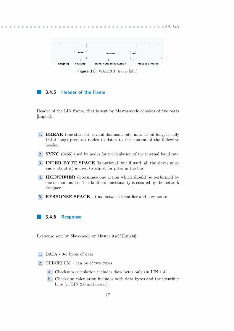
Two bus states are used: sleep-mode and active mode. For normal operationall nodes must be active, but after a specified time the nodes go back intoSleep-mode. If any node still needs communication trough the bus, it sends aWAKEUP frame. Only if all nodes are awake, Master-node can proceed withscheduling the next identifier. The example of functioning of the WAKEUPframe is shown on [3.8].
16
.........................................3.4. LIN
Figure 3.8: WAKEUP frame [Mic].
3.4.5 Header of the frame
Header of the LIN frame, that is sent by Master-node consists of five parts[Lup04]:..1. BREAK (one start bit, several dominant bits; min. 11-bit long, usually
13-bit long) prepares nodes to listen to the content of the followingheader...2. SYNC (0x55) used by nodes for recalculation of the internal baud rate...3. INTER BYTE SPACE (is optional, but if used, all the slaves mustknow about it) is used to adjust for jitter in the bus...4. IDENTIFIER determines one action which should be performed byone or more nodes. The faultless functionality is ensured by the networkdesigner...5. RESPONSE SPACE – time between identifier and a response.
3.4.6 Response
Response sent by Slave-node or Master itself [Lup04]:..1. DATA - 0-8 bytes of data...2. CHECKSUM – can be of two types:..a. Checksum calculation includes data bytes only (in LIN 1.3)..b. Checksum calculation includes both data bytes and the identifierbyte (in LIN 2.0 and newer)
17
3. Used Technologies: Networks..............................3.5 UART
3.5.1 General information
UART is a hard-integrated circuit for serial communication through theserial port. There are UART devices as standalone IC or as a part ofmicrocontrollers. MCU modules, unlike standalone modules, can control theoutput of UART. Conversion to the physical signal output can be generateddifferently on the transmitter side depending on the standard. There arethree of these recommended standards: RS-232, RS-422, RS-485. All of themdefine different methods for physical signal generation on the output. Theycan be different from MCU’s TTL class of digital circuit.
For communication between MCU’s UART module and a PC peripheraldevice, an additional circuit is needed. It is necessary because of differencesin transmission methods. An example can be useful: In TTL logic voltages onthe UART output can vary from 0 V (logical 0) to Vcc (logical 1). However,in case of RS-232 logical 0 is represented by a voltage in a range of 3-25 Vand logical 1 is in a range between -3 and -25. But from the software pointof view, MCU’s UART module and PC peripheral device are the same.
3.5.2 Types of UART
There are two forms of UART: UART and USART...1. The asynchronous form of communication:The transmitter generates the data clock internally. It is dependent onthe MCU clock cycles. Transmitter and receiver (two modules) shouldwork on the same baud rate (have the same clock cycle length). Thedata is usually transmitted in a byte...2. The synchronous form of communication:The transmitter generates a clock used to let the receiver side to recoverdata from the stream without transmitter’s baud rate. When the clocksignal is separated from data and sent on another line, very high transferrates can be achieved. Maximum possible transfer speed is 4 000 000bits per second, which is much greater than usual UART speeds. The
18
........................................3.6. JTAG
data is normally transferred in blocks. Thanks to this, USART modulecan generate data in a form comprehensive to many standard protocolsincluding LIN.
3.5.3 Communication
Communication happens on two independent lines TX (transmitter) and RX(receiver) in a form of simplex, half duplex or full duplex. The lines must bepulled up, so each side recognizes the existence of connection on the otherside. Data frame’s lengths can vary depending on configuration.
A frame consists of four parts:..1. Start bit (logic 0)..2. Data bits (1-14 bits)..3. The parity bit (optional), can be even or odd..4. Stop bits (1 or 2, logic 1)
Baud rate is a vital value, which specifies how fast the data is sent overthe bus in bits per second. The most used value is a standard of 9600. Thecomplete standard is called 9600 8N1, which means that the bus uses 9600baud rate, 8 bits of data, No parity and 1 stop bit.
3.6 JTAG
1149.1 IEEE [IEEa] standard provides testing of integrated circuits. JTAGconsists of several instruction modes. The most commonly used one isUSERCODE instruction, which provides upload of the code into the integratedcircuit. Also, is commonly used for so-called Boundary Scan, which is a testthat checks the correct functioning of all the pins on the chip. Another usageof JTAG is debugging of the controller.
19
3. Used Technologies: Networks..............................JTAG has four pins: TCK (test clock), TMS (test mode select), TDI (test
data input), TDO (test data output). Communication takes place on thepins TDI and TDO.
However, another version of this standard exists. IEEE 1149.7 [IEEb]standard can be controlled using only two pins - TCK as a clock signal andTMS as a data line.
Nowadays it is a vital interface for microcontrollers.
3.7 SWD
Another debugging tool designed and created specifically for ARM coreprocessors. Its main advantage is the fact that it requires only two wires:SWCLK (clock signal) and SWDIO (input and output). Besides SWD hashigher speed of communication comparing to JTAG.
20
Chapter 4
Used Technologies: Circuits, Componentsand Devices
4.1 Power supply
Electronic devices can be powered in different ways. One way is using abattery. Another one is auxiliary circuit, which can transform one form ofenergy (solar, wind etc.) into electricity. Or transformations from mainselectricity can be used.
Types of power supplies:..1. Linear regulators;..2. Switched-mode power supply.
4.1.1 Linear regulators
Linear regulators are relatively cheap and easy to implement. They providehigh stabilization of output voltage and wide range of input voltage. Thedisadvantages of such a method of power supply is a low efficiency.
21
4. Used Technologies: Circuits, Components and Devices...................4.1.2 Switched-mode power supply
Such power supply has up to 95-percent efficiency. It is an electronic circuitthat converts power by turning on and off special devices at high frequencies.There can be step-up(Boost) and step-down(Buck) converters. Proceedingpart shows only step-down converter since only it is used in the project.
4.1.3 Step-down converters
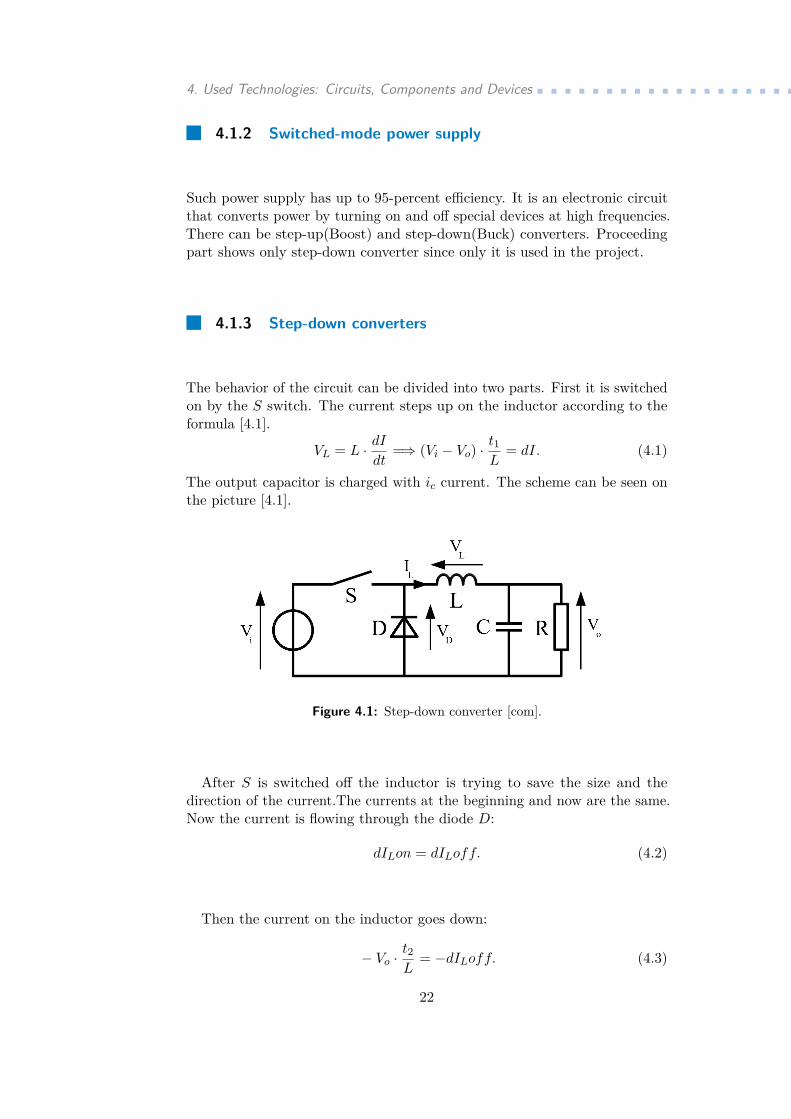
The behavior of the circuit can be divided into two parts. First it is switchedon by the S switch. The current steps up on the inductor according to theformula [4.1].
VL = L · dI
dt=⇒ (Vi − Vo) · t1
L= dI. (4.1)
The output capacitor is charged with ic current. The scheme can be seen onthe picture [4.1].
Figure 4.1: Step-down converter [com].
After S is switched off the inductor is trying to save the size and thedirection of the current.The currents at the beginning and now are the same.Now the current is flowing through the diode D:
dILon = dILoff. (4.2)
Then the current on the inductor goes down:
− Vo ·t2L
= −dILoff. (4.3)
22
...........................4.2. Types of components and packages
After combining all the three preceding equations the following equations canbe obtained:
Vo · t2 = (Vi − Vo) · t1 = Vi
[t1
t1 + t2
]= Vi
[t1T
]. (4.4)
This gives the output current [KRE97]:
Io = Ii ·Vi
Vo. (4.5)
4.2 Types of components and packages
The modern PCBs commonly use SMT components due to their betterproperties and the fact that they do not require drilling of the PCB.
4.2.1 Quad Flat Package
In this type of the case the pins are located on all four sides of the component.The number of pins vary from 32 to 304. This type is used for mediumefficient processors, for example STM32. It is possible to solder this case tothe PCB in domestic conditions. The most commonly used cases of this typeare TQFP, QFN, PLCC.
4.2.2 Dual in-line package
The pins are located on the two sides of the case. Are the best solution forsimpler micro-controllers, operational amplifiers. The common space betweenthe pins is 50 mils (1.27 mm). The most frequently used are SOIC, SOT,TSOP.
23
4. Used Technologies: Circuits, Components and Devices...................4.2.3 Ball Grid Array
The package is used for more efficient processors with large numbers of pinsorganized into matrices on the bottom side of the case. The advantage ofsuch a package is the fact that it lies directly on the PCB and sometimes itdoes not require soldering and thanks to that it does not overheat. It alsohas less induction (in comparison to QFP, for example) that is why it is usedfor faster circuits, for example DDR SDRAM. The main disadvantage is thefact that it requires machine mounting, which can be a problem for projectsin domestic conditions.
4.3 LED connection
LEDs are connected to the processor via resistors. The value of resistorsdepend completely on the parameters of the LEDs.The first important valueis the LED voltage VLED, another one in current on the LED ILED. Thenaccording to the Ohm’s law the wanted value of the resistor that is neededcan be calculated according to the formula:
R = Vcc − VLED
ILED. (4.6)
24

25
4. Used Technologies: Circuits, Components and Devices...................
Part II
Practical part
26
Chapter 5
Design of the module
5.1 Introduction
The module consists mainly of the processor, which is the heart and brain ofthe whole module. There are two LIN transceiver components connected tothe processor, a CAN transceiver, SWD.
All the schematics were made in OrCAD Capture, a PCB layout in Allegroby Cadence. This software is available in school laboratories. It is a verypowerful, though not easy to get to know tool for designing schematics andPCBs.
5.1.1 Hardware Requirements
The requirements to the hardware were the following:..1. The module should have 2 LIN bus interfaces...2. Configuration trough CAN bus...3. Allowed power supply of 12 V.
27
5. Design of the module ...................................4. Hardware opportunity to set the CAN node address for some value...5. Small size of the device (recommended dimensions of 10 cm x 10 cm x 4cm as length x with x hight)...6. Low prices of unit components and their accessibility.
5.1.2 Proposal of the solution..1. This can be solved by translating LIN signals into USART communica-tion. This will require additional components, but requirements to theprocessor are reduced to two USART interfaces which are more common...2. CAN interface on the processor is required...3. The module will use step-down power converter so that the allowedworking voltage can be 3.3 V as well as 12 V...4. For CAN node address settings will be used a DIP switch which is reliable(saves the set value even after the power cut) and easy to use.
5.1.3 Bypass Capacitors
In all circuit parts bypass capacitors are used for reducing the effect noise ofother circuit elements can have on the protected component. These capacitorsremove the AC caused by ripple voltage that can be present on DC signal.The simple rule for choosing the bypass capacitor is that it should be at least1/10 of the resistance to the flow of current than what the resistor can offerfor the frequency signal that needs to be bypassed. It needs to be put asclose as possible to the Vcc pin to lower as much as possible the inductance ofthe wire (information is from [Whaa].
5.1.4 Scheme and Components
The block scheme of the module is shown on the [5.1].
28
..................................... 5.1. Introduction
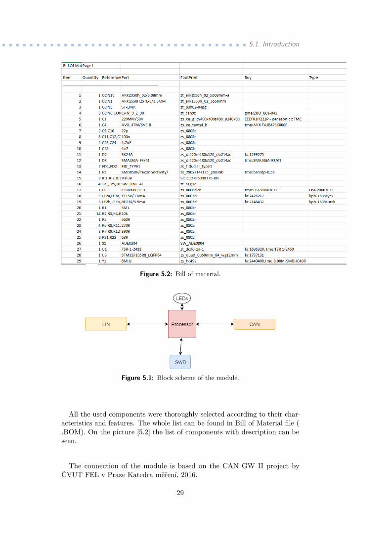
Figure 5.2: Bill of material.
Figure 5.1: Block scheme of the module.
All the used components were thoroughly selected according to their char-acteristics and features. The whole list can be found in Bill of Material file (.BOM). On the picture [5.2] the list of components with description can beseen.
The connection of the module is based on the CAN GW II project byČVUT FEL v Praze Katedra měření, 2016.
29

5. Design of the module .................................5.2 The Processor
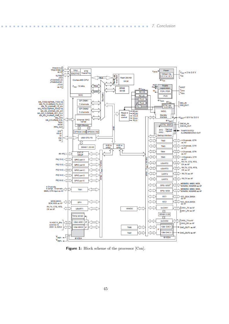
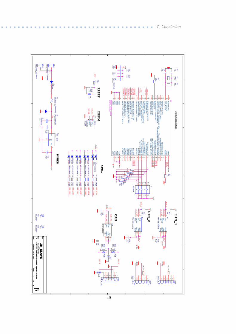
The processor STM32F105xx [Con] was used thanks to its wide range of usefulfeatures, simplicity in testing, its compatibility with a variety of commonperipheries, technical support in Prague. Besides that, this processor hasan ARM based architecture with 32-bit Cortex-M3 core, which I was wellacquainted with on the lectures in CTU. As I have already mentioned, thismicrocontroller is well balanced in means of functionality and simplicity. Theblock schematic of this processor is shown on the [1].
The main features of this microcontroller are:..1. 72 MHz maximum frequency;..2. 256 KB of 64-bit Flash memory; SRAM 64 Kbytes;..3. 14 communication interfaces:..a. 2 CAN interfaces (2.0B Active);..b. 3 SPI;..c. USB 2.0;..d. 10/100 Ethernet;..e. 5 USARTS;..4. CRC calculation unit;..5. Debug mode;..6. Low power.
This of course led to meeting of all the requirements that were put on thecontrolling of the module.
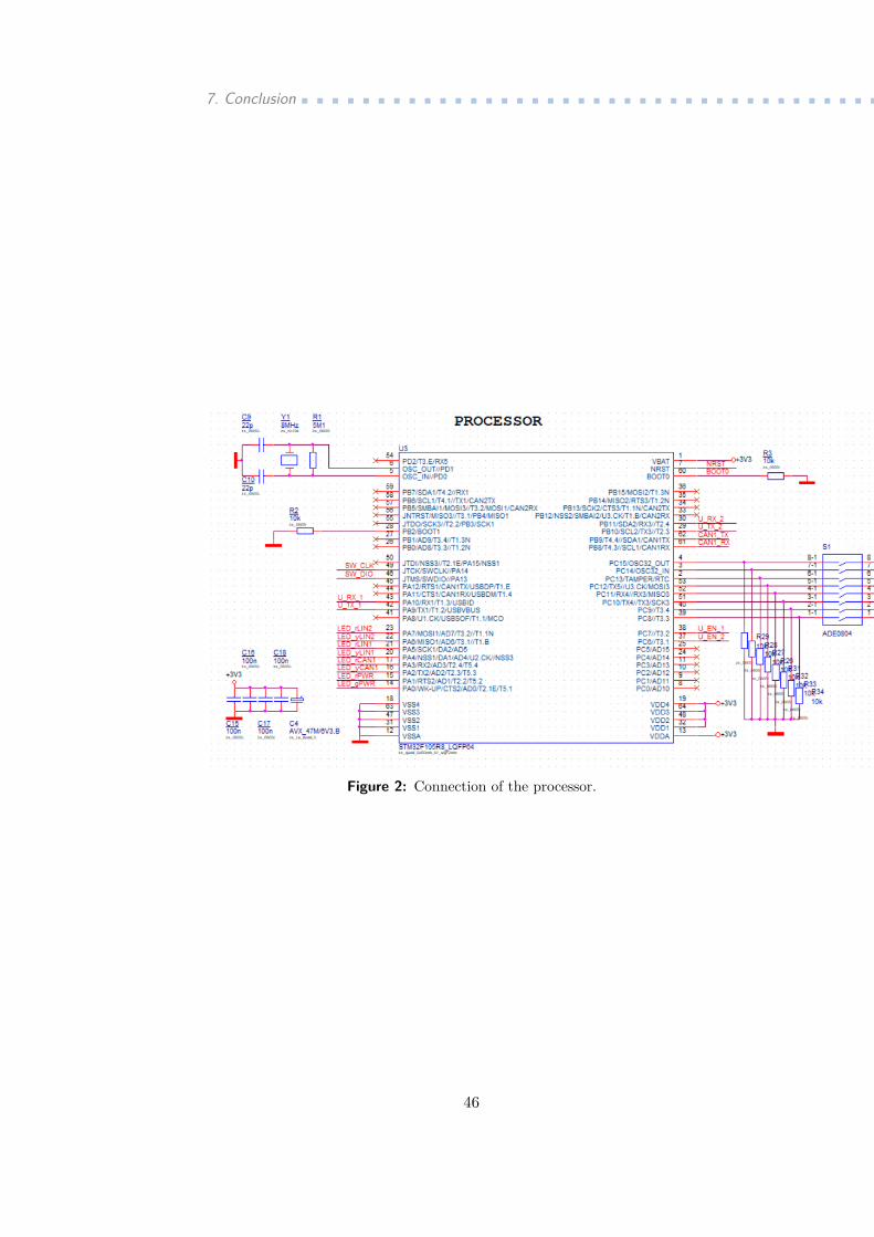
There is a connection of the processor on [2]
There is an external oscillator for higher precision. Also, a connection ofDIP switch can be observed. It will be used later for changing between 8possible modes or signals on the LIN bus.
The connection of the Reset circuit is the following: [5.3].
30
................................... 5.3. Power converter
Figure 5.3: Reset.
To prevent spurious resets, it is necessary to connect the NRST pin to acapacitor.
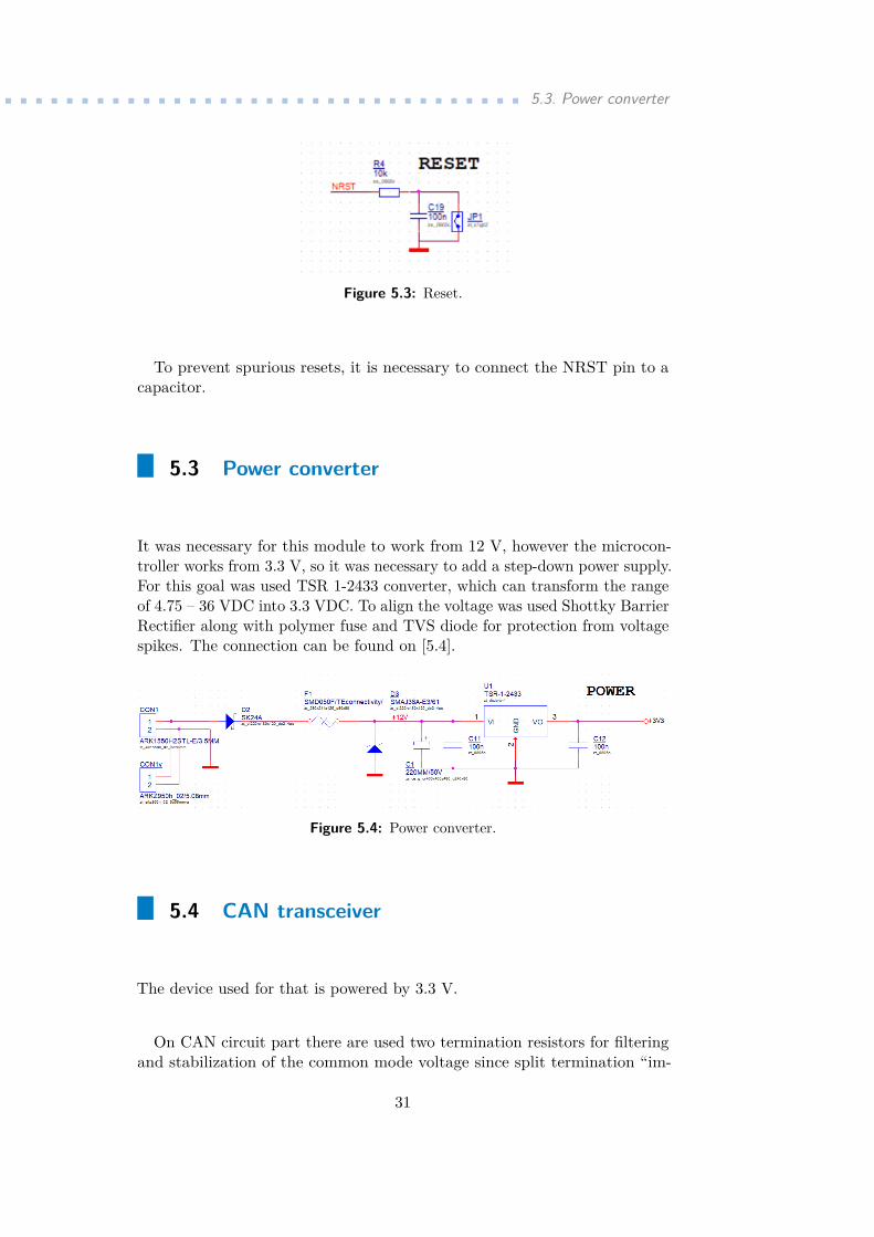
5.3 Power converter
It was necessary for this module to work from 12 V, however the microcon-troller works from 3.3 V, so it was necessary to add a step-down power supply.For this goal was used TSR 1-2433 converter, which can transform the rangeof 4.75 – 36 VDC into 3.3 VDC. To align the voltage was used Shottky BarrierRectifier along with polymer fuse and TVS diode for protection from voltagespikes. The connection can be found on [5.4].
Figure 5.4: Power converter.
5.4 CAN transceiver
The device used for that is powered by 3.3 V.
On CAN circuit part there are used two termination resistors for filteringand stabilization of the common mode voltage since split termination “im-
31
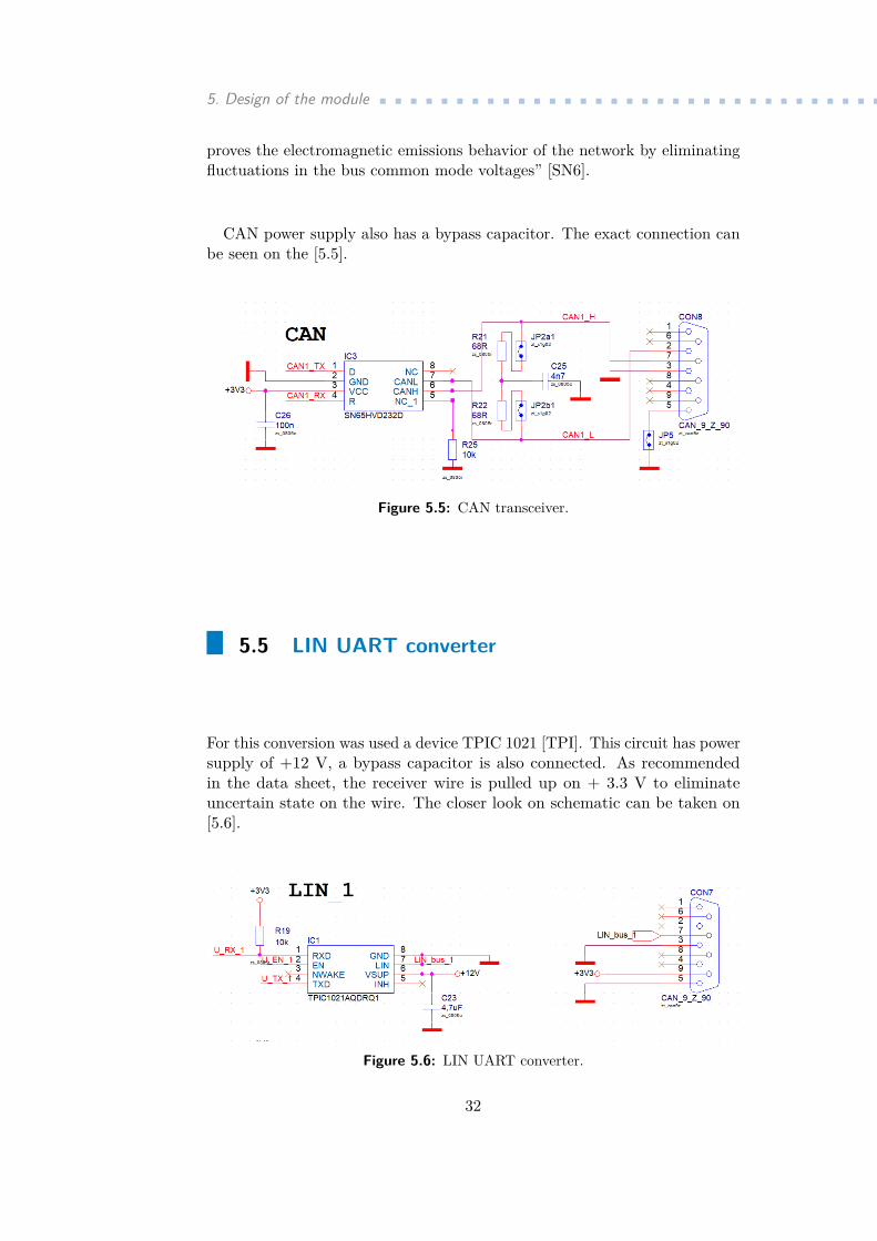
5. Design of the module .................................proves the electromagnetic emissions behavior of the network by eliminatingfluctuations in the bus common mode voltages” [SN6].
CAN power supply also has a bypass capacitor. The exact connection canbe seen on the [5.5].
Figure 5.5: CAN transceiver.
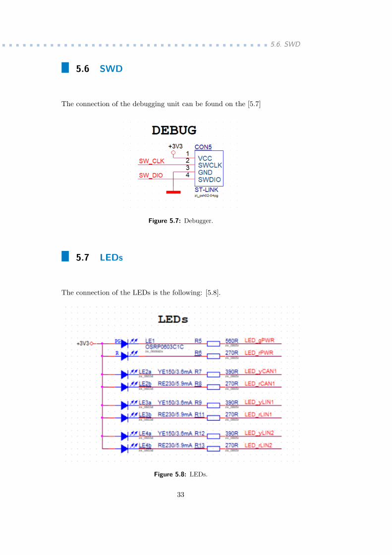
5.5 LIN UART converter
For this conversion was used a device TPIC 1021 [TPI]. This circuit has powersupply of +12 V, a bypass capacitor is also connected. As recommendedin the data sheet, the receiver wire is pulled up on + 3.3 V to eliminateuncertain state on the wire. The closer look on schematic can be taken on[5.6].
Figure 5.6: LIN UART converter.
32
........................................ 5.6. SWD
5.6 SWD
The connection of the debugging unit can be found on the [5.7]
Figure 5.7: Debugger.
5.7 LEDs
The connection of the LEDs is the following: [5.8].
Figure 5.8: LEDs.
33

5. Design of the module .................................The values of the resistors were calculated according to the formula [(4.6)].
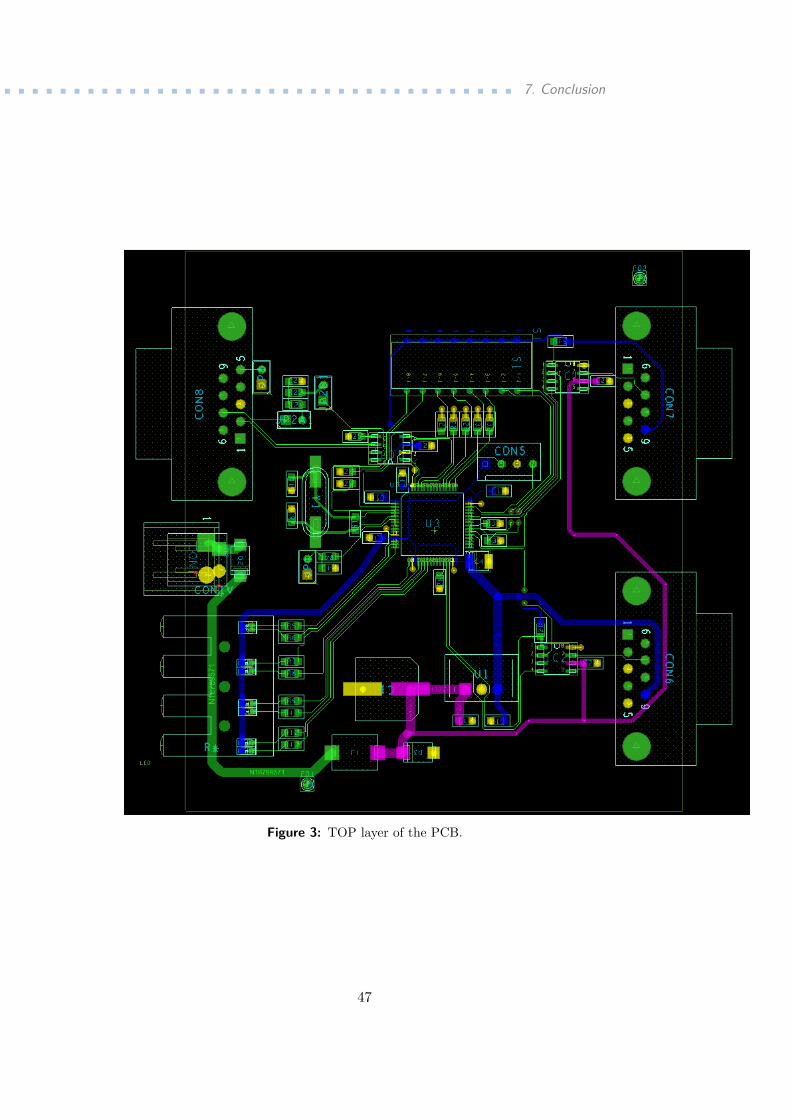
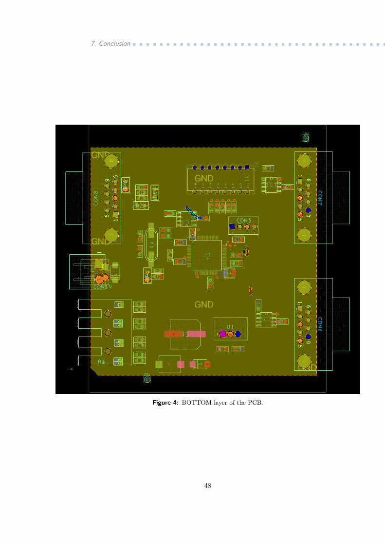
The PCB design was made in the Cadence Allegro software. The oututcan be seen on the [3] and [4].
34
Chapter 6
Program
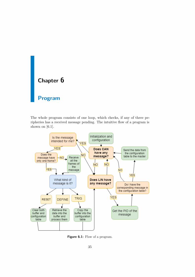
The whole program consists of one loop, which checks, if any of three pe-ripheries has a received message pending. The intuitive flow of a program isshown on [6.1].
Figure 6.1: Flow of a program.
35
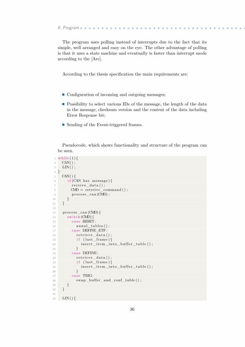
6. Program.......................................The program uses polling instead of interrupts due to the fact that its
simple, well arranged and easy on the eye. The other advantage of pollingis that it uses a state machine and eventually is faster than interrupt modeaccording to the [Arc].
According to the thesis specification the main requirements are:
. Configuration of incoming and outgoing messages;. Possibility to select various IDs of the message, the length of the datain the message, checksum version and the content of the data includingError Response bit;. Sending of the Event-triggered frames.
Pseudocode, which shows functionality and structure of the program canbe seen.
1 whi le (1 ) {2 CAN( ) ;3 LIN ( ) ;4 }5 CAN( ) {6 i f (CAN has message ) {7 rece ive_data ( ) ;8 CMD = retreive_command ( ) ;9 process_can (CMD) ;
10 }11 }12
13 process_can (CMD) {14 switch (CMD) {15 case RESET:16 annul_tables ( ) ;17 case DEFINE_ETF:18 r e t r i eve_data ( ) ;19 i f ( last_frame ) {20 insert_item_into_buf fer_table ( ) ;21 }22 case DEFINE:23 r e t r i eve_data ( ) ;24 i f ( last_frame ) {25 insert_item_into_buf fer_table ( ) ;26 }27 case TRIG:28 swap_buffer_and_conf_table ( ) ;29 }30 }31
32 LIN ( ) {
36
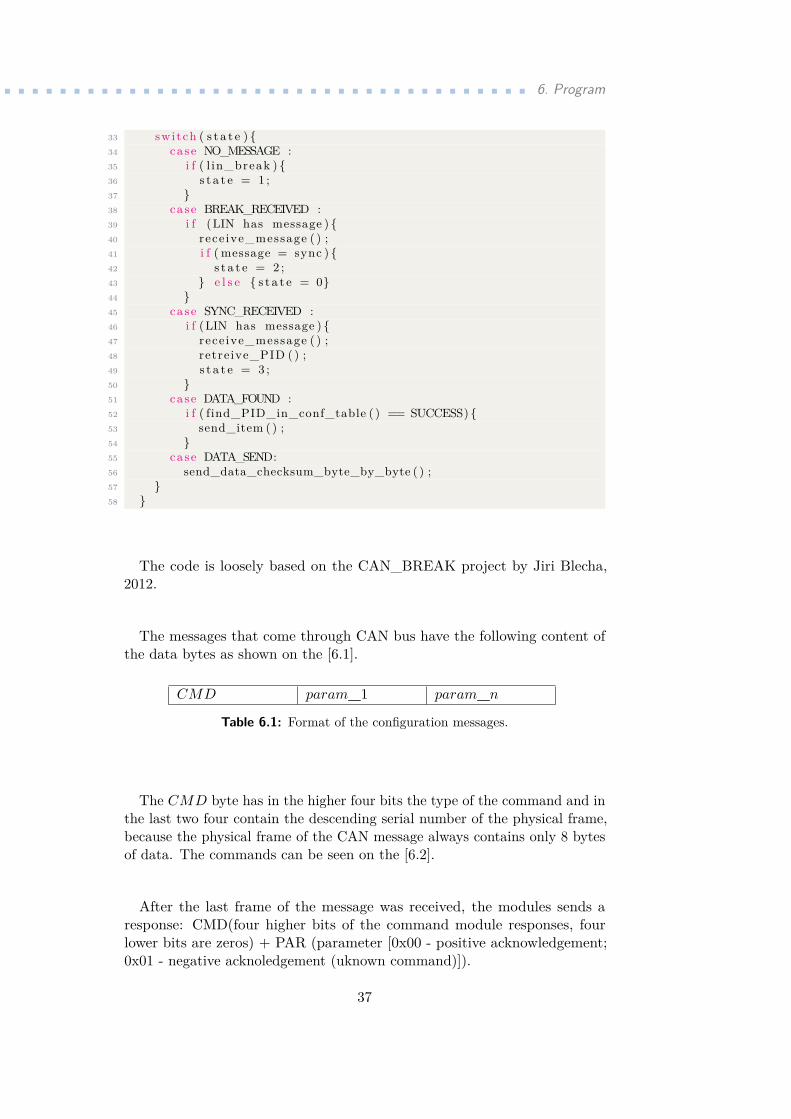
....................................... 6. Program
33 switch ( s t a t e ) {34 case NO_MESSAGE :35 i f ( l in_break ) {36 s t a t e = 1 ;37 }38 case BREAK_RECEIVED :39 i f (LIN has message ) {40 rece ive_message ( ) ;41 i f ( message = sync ) {42 s t a t e = 2 ;43 } e l s e { s t a t e = 0}44 }45 case SYNC_RECEIVED :46 i f (LIN has message ) {47 rece ive_message ( ) ;48 retreive_PID ( ) ;49 s t a t e = 3 ;50 }51 case DATA_FOUND :52 i f ( find_PID_in_conf_table ( ) == SUCCESS) {53 send_item ( ) ;54 }55 case DATA_SEND:56 send_data_checksum_byte_by_byte ( ) ;57 }58 }
The code is loosely based on the CAN_BREAK project by Jiri Blecha,2012.
The messages that come through CAN bus have the following content ofthe data bytes as shown on the [6.1].
CMD param_1 param_n
Table 6.1: Format of the configuration messages.
The CMD byte has in the higher four bits the type of the command and inthe last two four contain the descending serial number of the physical frame,because the physical frame of the CAN message always contains only 8 bytesof data. The commands can be seen on the [6.2].
After the last frame of the message was received, the modules sends aresponse: CMD(four higher bits of the command module responses, fourlower bits are zeros) + PAR (parameter [0x00 - positive acknowledgement;0x01 - negative acknoledgement (uknown command)]).
37
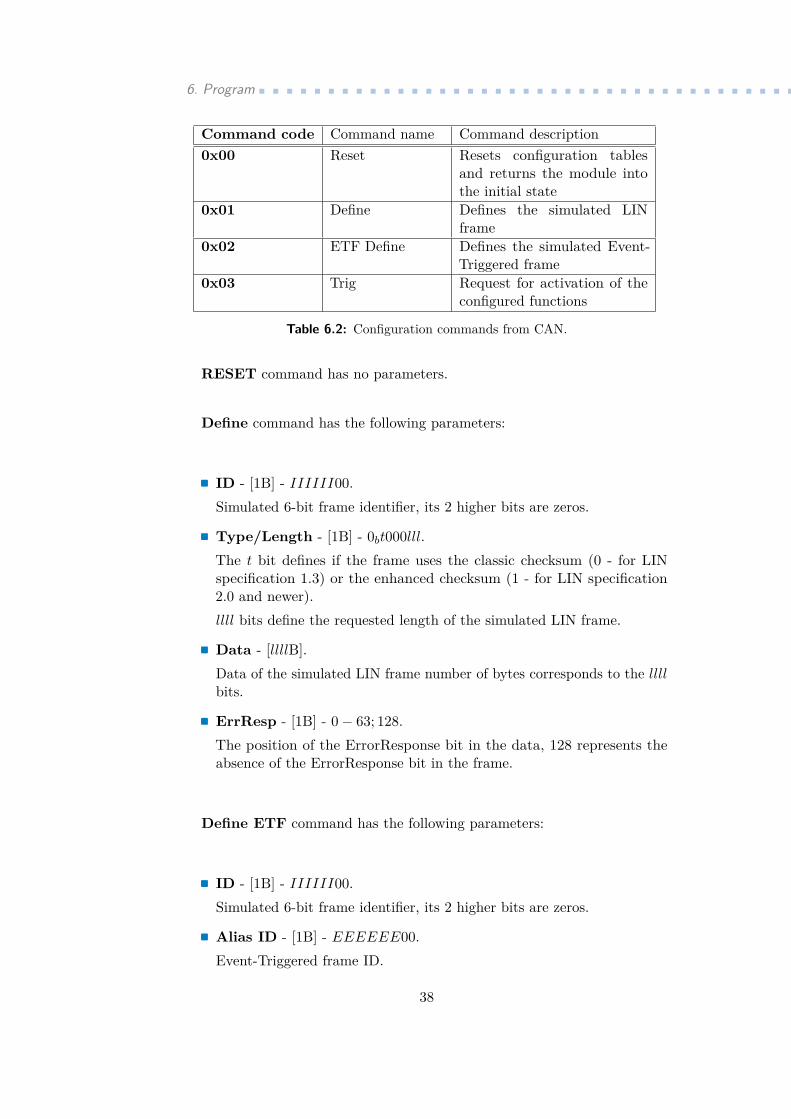
6. Program.......................................Command code Command name Command description0x00 Reset Resets configuration tables
and returns the module intothe initial state
0x01 Define Defines the simulated LINframe
0x02 ETF Define Defines the simulated Event-Triggered frame
0x03 Trig Request for activation of theconfigured functions
Table 6.2: Configuration commands from CAN.
RESET command has no parameters.
Define command has the following parameters:
. ID - [1B] - IIIIII00.Simulated 6-bit frame identifier, its 2 higher bits are zeros..Type/Length - [1B] - 0bt000lll.The t bit defines if the frame uses the classic checksum (0 - for LINspecification 1.3) or the enhanced checksum (1 - for LIN specification2.0 and newer).llll bits define the requested length of the simulated LIN frame..Data - [llllB].Data of the simulated LIN frame number of bytes corresponds to the llllbits.. ErrResp - [1B] - 0− 63; 128.The position of the ErrorResponse bit in the data, 128 represents theabsence of the ErrorResponse bit in the frame.
Define ETF command has the following parameters:
. ID - [1B] - IIIIII00.Simulated 6-bit frame identifier, its 2 higher bits are zeros..Alias ID - [1B] - EEEEEE00.Event-Triggered frame ID.
38
....................................... 6. Program
.Type/Length - [1B] - 0bt000lll.The t bit defines if the frame uses the classic checksum (0 - for LINspecification 1.3) or the enhanced checksum (1 - for LIN specification2.0 and newer).llll bits define the requested length of the simulated LIN frame..Data - [llllB].Data of the simulated LIN frame number of bytes corresponds to the llllbits.. ErrResp - [1B] - 0− 63; 128.The position of the ErrorResponse bit in the data, 128 represents theabsence of the ErrorResponse bit in the frame.
More information on this can be found in document LIN Slave, ČVUTFEL v Praze Katedra měření, 2018.
39

40
Chapter 7
Conclusion
The main aim of this bachelor thesis was designing and realization of thehardware module and implementing the software for it. The requirements tothe module were two LIN and one CAN connectors, the module shoud beable to simulate the behavior of LIN slaves according to the configurationmessages from CAN bus.
To fulfill this, I suggested the connection of all the components (wiringdiagram). After it was confirmed, I made the design of the PCB. After thePCB was printed out and all the components were soldered to it by mysupervisor, the module was tested. During the testing of the module it wasfound out, that I made some minor mistakes in the wiring diagram, whichwere solved by my supervisor.
The output module has two layers PCB and equipped with the requiredperipheries (LIN, CAN, SWD). The size of the PCB is saved within desireddimensions and all the components are optimized according to their function-ality, size and price. It uses the power of 12 V. This meets all the requirementsintroduced in the specification of the thesis.
The module can recognize the input data from CAN bus, process it andsave to the configuration table. It also can react to the headers that comefrom the LIN bus by sending the corresponding items from the configurationtable, both unconditional and Event-Triggered. The module responds tofound errors in the headers by setting the Error Response bit. This allowsmonitor problems on the LIN bus. This allows to meet all the softwarerequirements to module.
41

7. Conclusion......................................It is supposed, that in the future, the module will be able to simulate
more than one LIN slave (at least two). This is possible due to additionalconnector on the module and the fact, that the code structure allows to usetwo USARTs with only minor changes in the main loop.
Working in the Cadence IDE made a great contribution to my skills,because I have never designed a PCB before. I also learned how to work withdocumentation, found new things for myself during writing of the code andhad a deeper look on the hardware implementation.
42

43

7. Conclusion......................................
Appendices
44
...................................... 7. Conclusion
Figure 1: Block scheme of the processor [Con].
45
7. Conclusion......................................
Figure 2: Connection of the processor.
46
...................................... 7. Conclusion
Figure 3: TOP layer of the PCB.
47
7. Conclusion......................................
Figure 4: BOTTOM layer of the PCB.
48
...................................... 7. Conclusion
55
44
33
22
11
DD
CC
BB
AA
PROCESSOR
DEBUG
RESET
LEDs
POWER
LIN_1
LIN_2
CAN
LIN
_b
us_
2
LIN
_b
us_
1
+3
V3
+3
V3
+3
V3 +
3V
3
+3
V3
+3
V3
+3
V3
+1
2V
+3
V3
+3
V3
+3
V3
+1
2V
+3
V3
+3
V3
+3
V3
Title
Siz
eD
ocu
men
t Nu
mb
er
Rev
Date
:S
heet
of
CV
UT
-FE
L, A
leksan
dra
Pere
verz
eva
; Su
pervis
or: J
iri No
vak
1
LIN
_S
LA
VE
B
11
Satu
rday, A
pril 2
8, 2
01
8
Title
Siz
eD
ocu
men
t Nu
mb
er
Rev
Date
:S
heet
of
CV
UT
-FE
L, A
leksan
dra
Pere
verz
eva
; Su
pervis
or: J
iri No
vak
1
LIN
_S
LA
VE
B
11
Satu
rday, A
pril 2
8, 2
01
8
Title
Siz
eD
ocu
men
t Nu
mb
er
Rev
Date
:S
heet
of
CV
UT
-FE
L, A
leksan
dra
Pere
verz
eva
; Su
pervis
or: J
iri No
vak
1
LIN
_S
LA
VE
B
11
Satu
rday, A
pril 2
8, 2
01
8
JP
2b
1zt_
s1
g0
2
CO
N1
zt_a
rk15
50
h_
02
_3
o5
0m
m
AR
K1
55
0H
2S
TL
-E/3
.5M
M
12 C1
51
00
nzs_0805c
U1
TS
R-1
-24
33
zt_dcdc-ts
r-1
GND2
VI
1V
O3
CO
N5
zt_psh0
2-0
4pg
ST
-LIN
K
VC
C1
SW
CLK
2
SW
DIO
4G
ND
3
C1
11
00
nzs_0805c
R7
39
0R
zs_
08
05
r
R4
10
kzs
_0
80
5r
FD
1F
ID_
TY
PE
1zs
_fid
ucia
l_ty
pe
1
C2
61
00
nzs_0805c
R2
9
10
k
zs_
08
05
r
D3
SM
AJ3
6A
-E3
/61
zs_
di2
20
re1
80
x12
0_
do
21
4a
c
CO
N1
v
zt_a
rkz95
0h_
02
_5
o0
8m
m-a
AR
KZ
95
0h
_0
2/5
.08
mm
12F
D2
FID
_T
YP
E1
zs_
fiducia
l_ty
pe
1
IC1
TP
IC1
02
1A
QD
RQ
1
RX
D1
EN
2
NW
AK
E3
TX
D4
GN
D8
LIN
7
VS
UP
6
INH
5
CO
N6
zt_ca
n9
z
CA
N_
9_
Z_
90
5 9 4 8 3 7 2 6 1
JP
5zt_
s1
g0
2
Y1
8M
Hz
zs_
hc4
9s
R3
2
10
k
zs_
08
05
r
C1
91
00
nzs_0805c
LE
2a
YE
15
0/3
.6m
Azs
_0
60
3d
LE
4a
YE
15
0/3
.6m
Azs
_0
60
3d
C2
44
,7u
Fzs_0805c
R1
32
70
Rzs
_0
80
5r
C2
54
n7
zs_0805c
R1
5M
1zs
_0
80
5r
R1
9
10
k
zs_
08
05
r
R8
27
0R
zs_
08
05
r
C4
AV
X_
47
M/6
V3
.Bzs_ce_tantal_b
R5
56
0R
zs_
08
05
r
U3
ST
M3
2F
10
5R
8_
LQ
FP
64
zs_
qua
d_
0o
50
mm
_6
4_
wg1
2m
m
VB
AT
1
PC
13/T
AM
PE
R/R
TC
2P
C14/O
SC
32_IN
3P
C15/O
SC
32_O
UT
4
OS
C_IN
//PD
05
OS
C_O
UT
//PD
16
NR
ST
7
PC
0/A
D10
8P
C1/A
D11
9P
C2/A
D12
10
PC
3/A
D13
11
VS
SA
12
VD
DA
13
PA
0/W
K-U
P/C
TS
2/A
D0/T
2.1
E/T
5.1
14
PA
1/R
TS
2/A
D1/T
2.2
/T5.2
15
PA
2/T
X2/A
D2/T
2.3
/T5.3
16
PA
3/R
X2/A
D3/T
2.4
/T5.4
17
VS
S4
18
VD
D4
19
PA
4/N
SS
1/D
A1/A
D4/U
2.C
K//N
SS
320
PA
5/S
CK
1/D
A2/A
D5
21
PA
6/M
ISO
1/A
D6/T
3.1
//T1.B
22
PA
7/M
OS
I1/A
D7/T
3.2
//T1.1
N23
PC
4/A
D14
24
PC
5/A
D15
25
PB
0/A
D8/T
3.3
//T1.2
N26
PB
1/A
D9/T
3.4
//T1.3
N27
PB
2/B
OO
T1
28
PB
10/S
CL2/T
X3//T
2.3
29
PB
11/S
DA
2/R
X3//T
2.4
30
VS
S1
31
VD
D1
32
PB
12/N
SS
2/S
MB
AI2
/U3.C
K/T
1.B
/CA
N2R
X33
PB
13/S
CK
2/C
TS
3/T
1.1
N/C
AN
2T
X34
PB
14/M
ISO
2/R
TS
3/T
1.2
N35
PB
15/M
OS
I2/T
1.3
N36
PC
6//T
3.1
37
PC
7//T
3.2
38
PC
8//T
3.3
39
PC
9//T
3.4
40
PA
8/U
1.C
K/U
SB
SO
F/T
1.1
/MC
O41
PA
9/T
X1/T
1.2
/US
BV
BU
S42
PA
10/R
X1/T
1.3
/US
BID
43
PA
11/C
TS
1/C
AN
1R
X/U
SB
DM
/T1.4
44
PA
12/R
TS
1/C
AN
1T
X/U
SB
DP
/T1.E
45
JT
MS
/SW
DIO
//PA
13
46
VS
S2
47
VD
D2
48
JT
CK
/SW
CLK
//PA
14
49
JT
DI/N
SS
3//T
2.1
E/P
A15/N
SS
150
PC
10/T
X4//T
X3/S
CK
351
PC
11/R
X4//R
X3/M
ISO
352
PC
12/T
X5//U
3.C
K/M
OS
I353
PD
2/T
3.E
/RX
554
JT
DO
/SC
K3//T
2.2
/PB
3/S
CK
155
JN
TR
ST
/MIS
O3//T
3.1
/PB
4/M
ISO
156
PB
5/S
MB
AI1
/MO
SI3
//T3.2
/MO
SI1
/CA
N2R
X57
PB
6/S
CL1/T
4.1
//TX
1/C
AN
2T
X58
PB
7/S
DA
1/T
4.2
//RX
159
BO
OT
060
PB
8/T
4.3
//SC
L1/C
AN
1R
X61
PB
9/T
4.4
//SD
A1/C
AN
1T
X62
VS
S3
63
VD
D3
64
LE
4b
RE
23
0/5
.9m
Azs
_0
60
3d
C2
34
,7u
Fzs_0805c
F1
SM
D0
50
F/T
Eco
nn
ectivity/
zs_
29
0x2
14
z12
5_
p9
0x9
0
R1
12
70
Rzs
_0
80
5r
R9
39
0R
zs_
08
05
r
LE
3a
YE
15
0/3
.6m
Azs
_0
60
3d
C1
61
00
nzs_0805c
R2
10
kzs
_0
80
5r
R2
0
10
k
zs_
08
05
r
PG
R
LE
1O
SR
P0
60
3C
1C
zs_
06
06
d2
x
C9
22
pzs_0805c
LE
3b
RE
23
0/5
.9m
Azs
_0
60
3d
+
C1
22
0M
M/5
0V
zs_ce_g_cy400x400z480_p240x80
R3
1
10
k
zs_
08
05
r
R2
6
10
k
zs_
08
05
r
R6
27
0R
zs_
08
05
r
CO
N8
CA
N_
9_
Z_
90
zt_ca
n9
z
5 9 4 8 3 7 2 6 1
JP
1zt_
s1
g0
2
IC3
SN
65
HV
D2
32
D
D1
GN
D2
VC
C3
R4
NC
8
CA
NL
7
CA
NH
6
NC
_1
5
R2
51
0k
zs_
08
05
r
C1
81
00
nzs_0805c
IC2
TP
IC1
02
1A
QD
RQ
1
RX
D1
EN
2
NW
AK
E3
TX
D4
GN
D8
LIN
7
VS
UP
6
INH
5
R2
16
8R
zs_
08
05
r
D2
SK
24
Azs
_di2
20
re1
80
x12
0_
do
21
4a
c
R2
7
10
k
zs_
08
05
r
R3
3
10
k
zs_
08
05
r
C1
21
00
nzs_0805c
JP
2a1
zt_s1
g0
2
R1
23
90
Rzs
_0
80
5r
R2
26
8R
zs_
08
05
r
C1
02
2p
zs_0805c
R3
4
10
k
zs_
08
05
r
CO
N7
zt_ca
n9
z
CA
N_
9_
Z_
90
5 9 4 8 3 7 2 6 1
R3
10
kzs
_0
80
5r
S1
AD
E0
80
4
1-1
1 22-1
33-1
4-1
4 55-1
66-1
77-1
88-1
LE
2b
RE
23
0/5
.9m
Azs
_0
60
3d
C1
71
00
nzs_0805c
R2
8
10
k
zs_
08
05
r
BO
OT
0N
RS
T
U_
RX
_1
U_
TX
_1
CA
N1
_R
X
LE
D_
rPW
RL
ED
_yC
AN
1
LE
D_
yLIN
1L
ED
_rC
AN
1
CA
N1
_T
X
SW
_C
LK
SW
_D
IO
NR
ST
SW
_C
LK
SW
_D
IO
LE
D_
yLIN
2L
ED
_rL
IN1
LE
D_
rLIN
2
+1
2V
LE
D_
gP
WR
LE
D_
yCA
N1
LE
D_
yLIN
1
LE
D_
yLIN
2
LE
D_
rCA
N1
LE
D_
rLIN
1
LE
D_
rLIN
2
LE
D_
rPW
R
LE
D_
gP
WR
U_
RX
_2
U_
TX
_2
U_
RX
_1
U_
TX
_1
LIN
_b
us_
1U
_E
N_
1
U_
RX
_2
U_
EN
_2
LIN
_b
us_
2
U_
TX
_2
U_
EN
_1
U_
EN
_2
CA
N1
_H
CA
N1
_T
X
CA
N1
_R
X
CA
N1
_L
49

50
Appendix A
Bibliography
[12] , Lin network for vehicle applications, nov 2012.
[Arc] Archived: Benchmarking single-point performance on nationalinstruments real-time hardware - national instruments, http://www.ni.com/white-paper/5423/en/, (Accessed on 05/21/2018).
[Bos12] Bosch, Wayback machine, https://web.archive.org/web/20151211125301/http://www.bosch-semiconductors.de/media/ubk_semiconductors/pdf_1/canliteratur/can_fd_spec.pdf, 04 2012, (Accessed on 04/29/2018).
[CAN] Can in automation (cia): History of the can technology, https://www.can-cia.org/can-knowledge/can/can-history/, (Ac-cessed on 04/29/2018).
[com] CyrilB commonswiki, File:buck conventions.svg - wikimedia com-mons, https://commons.wikimedia.org/w/index.php?curid=617371, (Accessed on 04/30/2018).
[Con] Connectivity line, arm R©-based 32-bit mcu with 64/256 kb flash,usb otg, ethernet, 10 timers, 2 cans, 2 adcs, 14 communica-tion interfaces, http://www.st.com/resource/en/datasheet/cd00220364.pdf, (Accessed on 04/30/2018).
[DEK+01] John V. DeNuto, Stephen Ewbank, Francis Kleja, Christopher A.Lupini, and Robert A. Perisho, Lin bus and its potential for usein distributed multiplex applications, SAE 2001 World Congress,SAE International, mar 2001.
51
A. Bibliography.....................................[Emu] Emulin, http://www.ihr.de/index.php/en/products/
101-produkte-lin-english/390-emulin-english, (Accessedon 05/10/2018).
[HMS02] Motorola Hamed M. Sanogo, Implementing the can protocolin 3g equipment designs | ee times, https://www.eetimes.com/document.asp?doc_id=1206484, 12 2002, (Accessed on04/29/2018).
[htt] https://upload.wikimedia.org/wikipedia/commons/5/5e/can-bus-frame_in_base_format_without_stuffbits.svg, https://upload.wikimedia.org/wikipedia/commons/5/5e/CAN-Bus-frame_in_base_format_without_stuffbits.svg,(Accessed on 04/29/2018).
[IEEa] Ieee 1149.1-2013 - ieee standard for test access port and boundary-scan architecture, https://standards.ieee.org/findstds/standard/1149.1-2013.html, (Accessed on 05/21/2018).
[IEEb] Ieee 1149.7 - texas instruments wiki, http://processors.wiki.ti.com/index.php/IEEE_1149.7, (Accessed on 05/21/2018).
[ISOa] Iso 11519-1:1994 - road vehicles – low-speed serial data communi-cation – part 1: General and definitions, https://www.iso.org/standard/19469.html, (Accessed on 05/23/2018).
[ISOb] Iso 11898-1:2015 - road vehicles – controller area network (can) –part 1: Data link layer and physical signalling, https://www.iso.org/standard/63648.html, (Accessed on 05/21/2018).
[ISOc] Iso 17987-1:2016 - road vehicles – local interconnect network (lin)– part 1: General information and use case definition, https://www.iso.org/standard/61222.html, (Accessed on 05/21/2018).
[ISOd] Iso 9141-2:1994(en), road vehicles — diagnostic systems —part 2: Carb requirements for interchange of digital in-formation, https://www.iso.org/obp/ui/#iso:std:iso:9141:-2:ed-1:v1:en, (Accessed on 05/21/2018).
[ISOe] Iso/cd 17987-8 - road vehicles – local interconnect network (lin)– part 8: Electrical physical layer (epl) specification : Lin overdc powerline (dc-lin), https://www.iso.org/standard/71044.html, (Accessed on 05/21/2018).
[KRE97] A. KREJČIŘÍK, Napájecí zdroje i. 1.vyd., Praha: BEN, ISBN80-86056-02-3., 1997.
[Leo] Leonard-lin-bus.png, https://cecas.clemson.edu/cvel/auto/Buses/images/Leonard-LIN-BUS.png, (Accessed on05/11/2018).
52
..................................... A. Bibliography
[Lup04] Christopher A. Lupini, Vehicle multiplex communication, SAEInternational, may 2004.
[Med] Media access control (mac layer) - definition, http://ecomputernotes.com/computernetworkingnotes/communication-networks/media-access-control, (Accessedon 05/14/2018).
[Mic] Microchip, Lin frame types - developer help, http://microchipdeveloper.com/lin:protocol-dll-frame-types,(Accessed on 04/30/2018).
[Mos08] Anthony Moschella, Simulation of lin clusters for reducing in-vehicle network development and validation costs, SAE WorldCongress & Exhibition, SAE International, apr 2008.
[Phy] Phytools, Phytools - can-to-lin interface, can repeater, lin slave,industry-best support, https://www.phytools.com/CAN_to_LIN_Interface_CAN_Repeater_LIN_Slave_s/1829.htm, (Accessedon 04/29/2018).
[Ruf02] Matthew Ruff, Implementing local interconnect network (lin) slavenodes, SAE 2002 World Congress & Exhibition, SAE International,mar 2002.
[Sch] Schematic-of-a-typical-in-vehicle-network-architecture-of-a-modern-automobile-12.png, https://www.researchgate.net/profile/Jonathan_Petit/publication/266780575/figure/fig1/AS:295746776649730@1447522934824/Schematic-of-a-typical-in-vehicle-network-architecture-of-a-modern-automobile-12.png, (Accessed on 05/11/2018).
[sCN] Distributed systems and FEL CVUT Computer Networks,Testing the distributed systems for the harsh environment,https://moodle.fel.cvut.cz/pluginfile.php/83967/mod_resource/content/3/6_Communication%20Basics_cz.pdf,(Accessed on 05/14/2018).
[SN6] Sn65hvd23x 3.3-v can bus transceivers datasheet (rev. o), http://www.ti.com/lit/ds/symlink/sn65hvd231.pdf, (Accessed on04/30/2018).
[TPI] Tpic1021 lin physical interface datasheet (rev. d), http://www.ti.com/lit/ds/symlink/tpic1021.pdf, (Accessed on 04/30/2018).
[Whaa] What is a bypass capacitor?, http://www.learningaboutelectronics.com/Articles/What-is-a-bypass-capacitor.html, (Accessed on 04/30/2018).
53

A. Bibliography.....................................[Whab] What is cyclic redundancy check (crc)? - definition from
techopedia, https://www.techopedia.com/definition/1793/cyclic-redundancy-check-crc, (Accessed on 05/21/2018).
[Zhu10] Yu. Zhu, Can and fpga communication engineering: Implementa-tion of a can bus based measurement system on an fpga develop-ment kit., Hamburg: Diplomica Verlag., 2010.
54
ZADÁNÍ BAKALÁŘSKÉ PRÁCE
I. OSOBNÍ A STUDIJNÍ ÚDAJE
453454Osobní číslo:AleksandraJméno:PereverzevaPříjmení:
Fakulta elektrotechnickáFakulta/ústav:
Zadávající katedra/ústav: Katedra měření
Otevřená informatikaStudijní program:
Počítačové systémyStudijní obor:
II. ÚDAJE K BAKALÁŘSKÉ PRÁCI
Název bakalářské práce:
Simulátor LIN Slave
Název bakalářské práce anglicky:
LIN Slave Simulator
Pokyny pro vypracování:Navrhněte a realizujte HW modul pro funkční simulaci uzlu typu Slave. Implementujte programové vybavení modulu,umožňující konfiguraci komunikačních rámců, a to jak vysílaných, tak přijímaných. Konfigurace jednotlivého rámce musíumožnit volbu identifikátoru, délky rámce, způsobu výpočtu kontrolního součtu rámce a datového obsahu rámce včetnědefinice ErrorResponse bitu. Modul musí podporovat vysílání rámců generovaných událostmi. Konfiguračním rozhranímmodulu bude CAN.
Seznam doporučené literatury:[1] Kocourek, P., Novák, J.: Přenos informace, Skripta ČVUT, Praha 2003[2] Lupini Ch.: Vehicle Multiplex Communication, SAE International 2004[3] ISO 17987 - LIN Standard
Jméno a pracoviště vedoucí(ho) bakalářské práce:
doc. Ing. Jiří Novák, Ph.D., K 13138 - katedra měření
Jméno a pracoviště druhé(ho) vedoucí(ho) nebo konzultanta(ky) bakalářské práce:
Termín odevzdání bakalářské práce: 25.05.2018Datum zadání bakalářské práce: 09.01.2018
Platnost zadání bakalářské práce:do konce letního semestru 2018/2019
_________________________________________________________________________________prof. Ing. Pavel Ripka, CSc.
podpis děkana(ky)podpis vedoucí(ho) ústavu/katedrydoc. Ing. Jiří Novák, Ph.D.
podpis vedoucí(ho) práce
III. PŘEVZETÍ ZADÁNÍStudentka bere na vědomí, že je povinna vypracovat bakalářskou práci samostatně, bez cizí pomoci, s výjimkou poskytnutých konzultací.Seznam použité literatury, jiných pramenů a jmen konzultantů je třeba uvést v bakalářské práci.
.Datum převzetí zadání Podpis studentky
© ČVUT v Praze, Design: ČVUT v Praze, VICCVUT-CZ-ZBP-2015.1


