Embed Size (px)
Citation preview
EEE4084F Exam 2013 Page 1 of 10
Digital Systems
EEE4084F
FINAL EXAM
5 June 2013
3 hours
Examination Prepared by
Simon Winberg
Last Modified 20-May-2013
REGULATIONS
This is a closed-book exam Scan through the questions quickly before starting so that you can plan your
strategy for answering the questions If you are caught cheating you will be referred to University Court for
expulsion procedures Answer on the answer sheets provided Make sure that you put your student name and
student number the course code EEE4084F and a title Final Exam on your answer sheet(s) Answer each section on a separate page
DO NOT TURN OVER UNTIL YOU ARE TOLD TO
Exam Structure Marked out of 100 marks Time per mark = 1min 48sec
RULES
bull You must write your name and student number on each answer book bull Write the question numbers attempted on the cover of each book bull Start each section on a new page bull Make sure that you cross out material you do not want marked Your first attempt at any question will be marked if two answers are found bull Use a part of your script to plan the facts for your written replies to questions so that you produce
carefully constructed responses bull Answer all questions and note that the time for each question relates to the marks allocated
Section 1
Short Answers (4 x 10 mark questions)
[40 marks]
pg 2 Pg 9
Section 3
Long Answers (2x questions)
[36 marks]
pg 6
Appendices
A Formulae
B Verilog cheatsheet
C detachable answer
sheet pg 8
Section 2
Multiple choice (5x 4-mark questions)
[20 marks]
Pg 4
Section 2
Multiple choice
(6x 4-mark questions) [24 marks]
pg 4
NB
EEE4084F Exam 2013 Page 2 of 10
Section 1 Short Answers [40 marks]
Question 11 [10 marks]
(a) Computation is generally performed using one of the following methods
1 A specialized hardware platform running dedicated software (eg an embedded system)
2 Application software running on a general purpose platform (eg a PC or supercomputer) or
3 Using a reconfigurable computing platform
Briefly contrast these three approaches highlighting types of applications that are well suited to certain
approaches and why they may or not be suitable to the others methods Ensure your answer is articulate and includes examples Figures are welcome but not a requirement [6 marks]
(b) Briefly explain what is meant by a ldquoreconfigurable computing platformrdquo and how FPGA-based reconfigurable
computing differs from microprocessor-based reconfigurable computing [4 marks]
Question 12 [10 marks]
Cloud Computing has shown a significant amount of popularity in recent years Carefully define what is meant by
cloud computing Write down you well considered view of how you think the next 5 years will treat cloud computing Ensure you clarify the advantages and disadvantages of cloud computing (Your answer needs to be logically
structured and well written to get better marks) [10 marks]
Question 13 [10 marks]
(a) The increase in GFLOPS for computer systems has shown exponential growth from the humble beginnings of
computing For example before the 1950s even 1MFLOP was unobtainable Around what decade (1950s 1960 1970 1980 or 1990) was an excess of 05GLOPS (ie 500MFLOPS) achieved for a processor [1 mark]
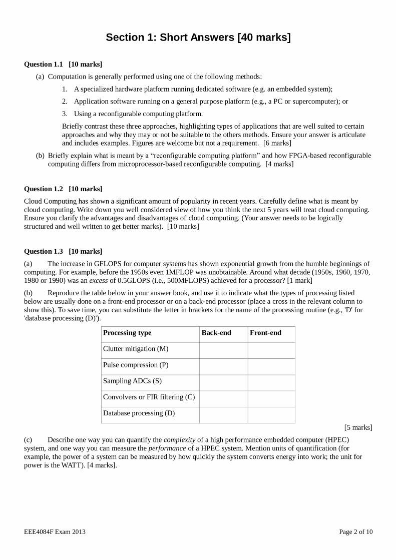
(b) Reproduce the table below in your answer book and use it to indicate what the types of processing listed
below are usually done on a front-end processor or on a back-end processor (place a cross in the relevant column to
show this) To save time you can substitute the letter in brackets for the name of the processing routine (eg D for database processing (D))
Processing type Back-end Front-end
Clutter mitigation (M)
Pulse compression (P)
Sampling ADCs (S)
Convolvers or FIR filtering (C)
Database processing (D)
[5 marks]
(c) Describe one way you can quantify the complexity of a high performance embedded computer (HPEC)
system and one way you can measure the performance of a HPEC system Mention units of quantification (for
example the power of a system can be measured by how quickly the system converts energy into work the unit for
power is the WATT) [4 marks]
EEE4084F Exam 2013 Page 3 of 10
Question 14 [10 marks]
(a) What is the difference between temporal computation and spatial computation [3 marks]
(b) RC platforms are typically built around the use of FPGAs These systems often include a CPLD in addition to
the FPGA What are the main differences between a FPGA and a CPLD Give a reason why a CPLD may
likely still be incorporated into a reconfigurable computing platform despite the platform having a much larger
(in terms of Les) and more powerful FPGA on the platform to do the bulk of the processing [4 marks]
(c) A particular platform can be supported by multiple ABIs For example the IBM Cell processor is supported
by both the commercial IBM SPE ABI and the open-source Linux Cell ABI yet the two ABIs are not
identical What is an ABI and why might different operating systems that can run on the same platform have different ABIs [3 marks]
EEE4084F Exam 2013 Page 4 of 10
Section 2 Multiple Choice [24 marks]
NOTE Choose only one option (ie either a b c d or e) for each question in this section
Q21 The quantization-noise related signal to noise ratio of a mid-range ADC was measured to be 58 bB What can
you say about the effective number of bits (ie ENOB) for this ADC (Select the most accurate answer)
(a) ENOB = 7
(b) ENOB lt 7
(c) ENOB = 8
(d) ENOB = 9
(e) ENOB gt= 10
[4 Marks]
Q22 What is another term for synchronous communications
(a) Non-blocking communications
(b) Blocking communications
(c) Handshaking communications
(d) Serialized transfers
(e) Untimed communications
[4 marks]
Q23 Consider that the following variables are defined
f = fraction of computation that can be parallelized n = number of processors for parallel case
Then according to Amdahlrsquos law the maximum speed-up achievable for the parallel case over a sequential
case is (chose one option below)
(a) Speedup = (1 ndash f) ( (1 ndash nf) )
(b) Speedup = (1 ndash f) (fn - 1)
(c) Speedup = 1 ( (1 ndash f) + fn )
(d) Speedup = f (f ndash 1)(n+1)
(e) Speedup = (n + 1) (1 ndash f)
[4 marks]
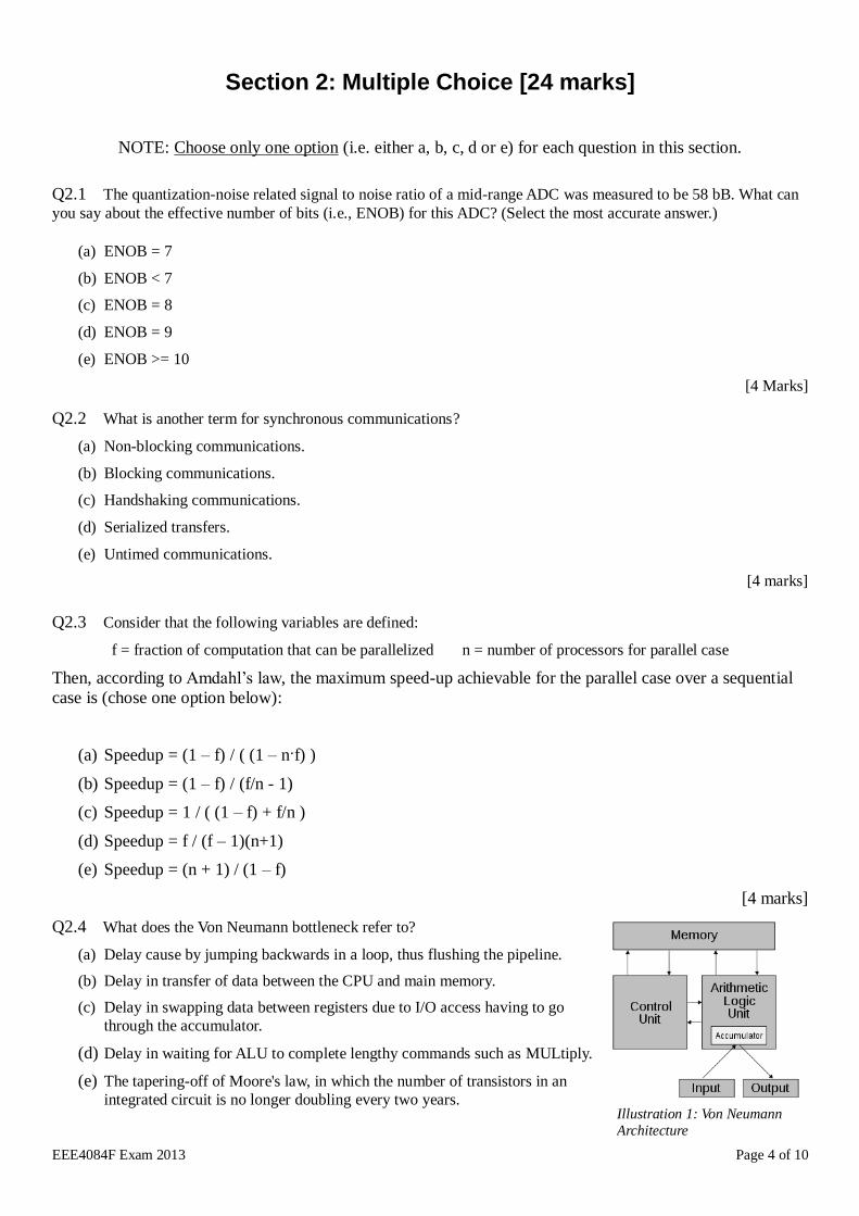
Q24 What does the Von Neumann bottleneck refer to
(a) Delay cause by jumping backwards in a loop thus flushing the pipeline
(b) Delay in transfer of data between the CPU and main memory
(c) Delay in swapping data between registers due to IO access having to go
through the accumulator
(d) Delay in waiting for ALU to complete lengthy commands such as MULtiply
(e) The tapering-off of Moores law in which the number of transistors in an
integrated circuit is no longer doubling every two years
Illustration 1 Von Neumann
Architecture
EEE4084F Exam 2013 Page 5 of 10
Q25 Which statement below is accurate concerning CMOS
(a) CMOS is more power hungry that TTL
(b) CMOS is not found in many ICs nowadays
(c) CMOS gates usually take less power and area on chip than either TTL or NMOS
(d) CMOS gates are usually much faster than TTL gates
(e) All the above statements are accurate
[4 marks]
Q26 Answer true or false to each question below (each answer is 1 mark)
(i) In computing the acronym MOSFET stands for lsquoMOSt Famous Electronic Transistorrsquo
(ii) The commonly used HPEC acronym SWAP refers to the lsquoSize Weight And Powerrsquo matric
(iii) Processing in an FPGA occurs within the IOBs as opposed to in the more passive CLBs
(iv) In general computing terminology VLSI stands for lsquoVery Large Systems Incorporatedrsquo
[4 x 1 mark each = 4 marks]
EEE4084F Exam 2013 Page 6 of 10
Section 3 Long Answers [36 marks]
Question 31 [15 marks]
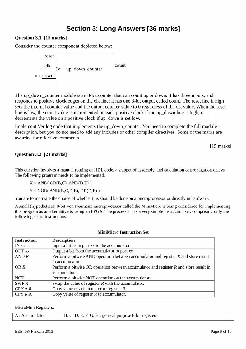
Consider the counter component depicted below
The up_down_counter module is an 8-bit counter that can count up or down It has three inputs and
responds to positive clock edges on the clk line it has one 8-bit output called count The reset line if high
sets the internal counter value and the output counter value to 0 regardless of the clk value When the reset
line is low the count value is incremented on each positive clock if the up_down line is high or it
decrements the value on a positive clock if up_down is set low
Implement Verilog code that implements the up_down_counter You need to complete the full module
description but you do not need to add any includes or other compiler directives Some of the marks are
awarded for effective comments
[15 marks]
Question 32 [21 marks]
This question involves a manual routing of HDL code a snippet of assembly and calculation of propagation delays
The following program needs to be implemented
X = AND( OR(BC) AND(DE) )
Y = NOR( AND(BCDE) OR(DE) )
You are to motivate the choice of whether this should be done on a microprocessor or directly in hardware
A small (hypothetical) 8-bit Von Neumann microprocessor called the MiniMicro is being considered for implementing
this program as an alternative to using an FPGA The processor has a very simple instruction set comprising only the following set of instructions
MiniMicro Instruction Set
Instruction Description
IN xx Input a bit from port xx to the accumulator
OUT xx Output a bit from the accumulator to port xx
AND R Perform a bitwise AND operation between accumulator and register R and store result
in accumulator
OR R Perform a bitwise OR operation between accumulator and register R and store result in
accumulator
NOT Perform a bitwise NOT operation on the accumulator
SWP R Swap the value of register R with the accumulator
CPY AR Copy value of accumulator to register R
CPY RA Copy value of register R to accumulator
MicroMini Registers
A Accumulator B C D E F G H general purpose 8-bit registers
up_down_counter
reset
clk
up_down
count
EEE4084F Exam 2013 Page 7 of 10
Assuming that inputs BCD and E are respectively connected to ports 0xF0 0xF1 0xF2 0xF3 and that X is at output
port address 0xF4 and Y at 0xF5 The assembly code below shows an example of computing X
MiniMicro code to calculate and output X
IN 0xF0
SWP B
IN 0xF1
OR B
SWP G G = inB OR inC
hellip add your code from here hellip
32 (a)
Complete the rest of the program which was started above in order to calculate and output Y You can assume that
your code will be pasted below the code above The MiniMicro has only 256 program memory addresses but that will
hopefully be more than adequate for the program Comments count for 3 of the marks
[7 marks]
32 (b)
If each instruction takes one clock cycle to complete and the processor has no pipelining then determine how long it
will take for your program to run (assuming no startup and end off operations are needed) The system clock for the
MiniMicro runs at 100Mhz
[3 marks]
32 (c)
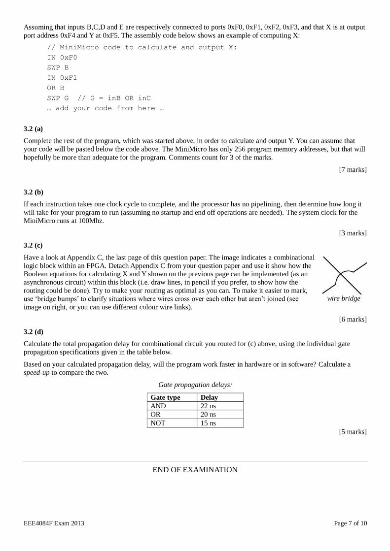
Have a look at Appendix C the last page of this question paper The image indicates a combinational
logic block within an FPGA Detach Appendix C from your question paper and use it show how the Boolean equations for calculating X and Y shown on the previous page can be implemented (as an
asynchronous circuit) within this block (ie draw lines in pencil if you prefer to show how the
routing could be done) Try to make your routing as optimal as you can To make it easier to mark use lsquobridge bumpsrsquo to clarify situations where wires cross over each other but arenrsquot joined (see
image on right or you can use different colour wire links)
[6 marks]
32 (d)
Calculate the total propagation delay for combinational circuit you routed for (c) above using the individual gate
propagation specifications given in the table below
Based on your calculated propagation delay will the program work faster in hardware or in software Calculate a speed-up to compare the two
Gate propagation delays
Gate type Delay
AND 22 ns
OR 20 ns
NOT 15 ns
[5 marks]
END OF EXAMINATION
wire bridge
EEE4084F Exam 2013 Page 8 of 10
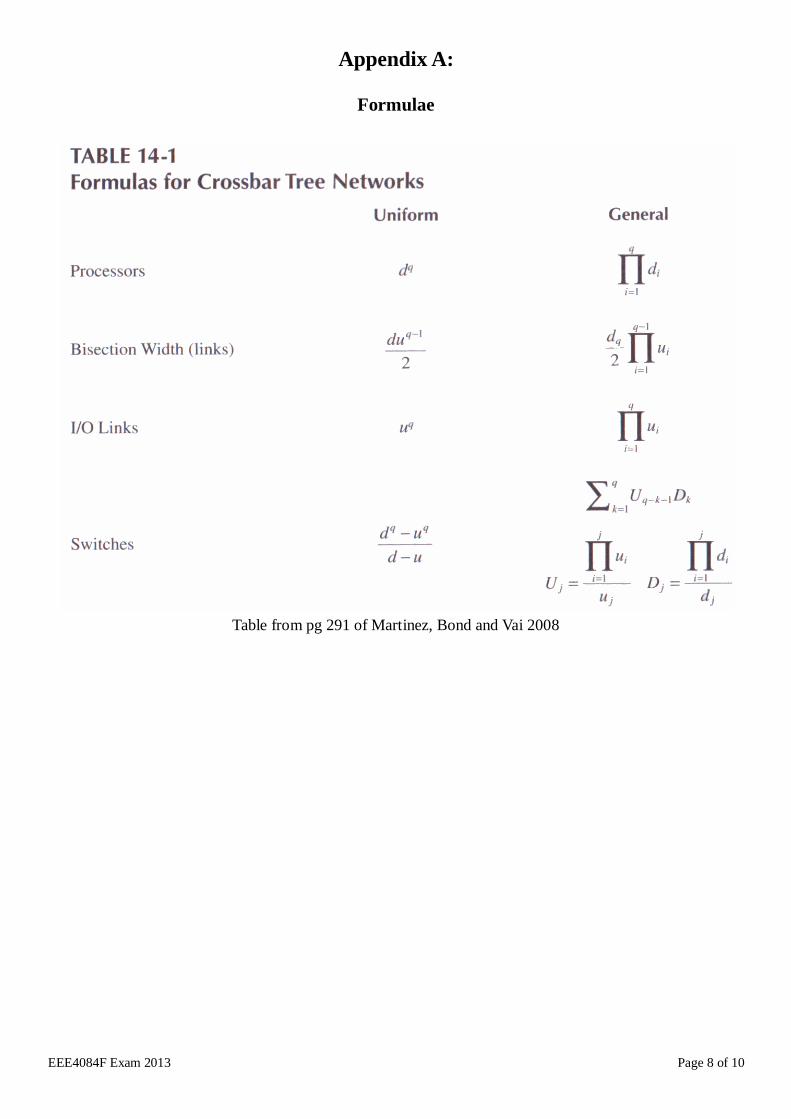
Appendix A
Formulae
Table from pg 291 of Martinez Bond and Vai 2008
EEE4084F Exam 2013 Page 9 of 10
Appendix B Verilog Cheat sheet
Numbers and constants
Example 4-bit constant 10 in binary hex and in
decimal 4rsquob1010 == 4rsquoha -- 4rsquod10
(numbers are unsigned by default)
Concatenation of bits using
4rsquob1011 == 2rsquob10 2rsquob11
Constants are declared using parameter
parameter myparam = 51
Operators
Arithmetic and (+) subtract (-) multiply ()
divide () and modulus () all provided
Shift left (ltlt) shift right (gtgt)
Relational ops equal (==) not-equal (=) less-
than (lt) less-than or equal (lt=) greater-than (gt)
greater-than or equal (gt=)
Bitwise ops and ( amp ) or ( | ) xor ( ˆ ) not ( ˜ )
Logical operators and (ampamp) or (||) not () note
that these work as in C eg (2 ampamp 1) == 1
Bit reduction operators [n] n=bit to extract
Conditional operator to multiplex result
Example (a==1) funcif1 funcif0
The above is equivalent to
((a==1) ampamp funcif1)
|| ((a=1) ampamp funcif0)
Registers and wires
Declaring a 4 bit wire with index starting at 0
wire [30] w
Declaring an 8 bit register
reg [70] r
Declaring a 32 element memory 8 bits wide
reg [70] mem [031]
Bit extract example
r[52] returns 4 bits between pos 2 to 5 inclusive
Assignment
Assignment to wires uses the assign primitive
outside an always block eg
assign mywire = a amp b
Registers are assigned to inside an always block
which specifies where the clock comes from eg
always(posedge myclock)
cnt = cnt + 1
Blocking vs unblocking assignment lt= vs =
The lt= assignment operator is non-blocking (ie
if use in an always(posedge) it will be
performed on every positive edge If you have
many non-blocking assignments they will all
updated in parallel The lt= operator must be used
inside an always block ndash you canrsquot use it in an
assign statement
The blocking assignment operator = can be used
in either an assign block or an always block But it
causes assignments to be performed in sequential
order This tends to result in slower circuits so
avoid using it (especially for synthesized circuits)
unless you have to
Case and if statements
Case and if statements are used inside an always
block to conditionally update state eg
always (posedge clock)
if (add1 ampamp add2) r lt= r+3
else if (add2) r lt= r+2
else if(add1) r lt= r+1
Note that we donrsquot need to specify what happens
when add1 and add2 are both false since the
default behavior is that r will not be updated
Equivalent function using a case statement
always (posedge clock)
case(add2add1)
2rsquob11 r lt= r+3
2rsquob10 r lt= r+2
2rsquob01 r lt= r+1
default r lt= r
endcase
Module declarations
Modules pass inputs outputs as wires by default
module ModName (
output reg [30] result register output
input [10] bitsin input clk )
hellip code hellip
endmodule
EEE4084F Exam 2013 Page 10 of 10
Appendix C Programmable Combinational Logic Block
Name _______________________ Student Number _______________________ Please detach and put in your answer book
EEE4084F Exam 2013 Page 2 of 10
Section 1 Short Answers [40 marks]
Question 11 [10 marks]
(a) Computation is generally performed using one of the following methods
1 A specialized hardware platform running dedicated software (eg an embedded system)
2 Application software running on a general purpose platform (eg a PC or supercomputer) or
3 Using a reconfigurable computing platform
Briefly contrast these three approaches highlighting types of applications that are well suited to certain
approaches and why they may or not be suitable to the others methods Ensure your answer is articulate and includes examples Figures are welcome but not a requirement [6 marks]
(b) Briefly explain what is meant by a ldquoreconfigurable computing platformrdquo and how FPGA-based reconfigurable
computing differs from microprocessor-based reconfigurable computing [4 marks]
Question 12 [10 marks]
Cloud Computing has shown a significant amount of popularity in recent years Carefully define what is meant by
cloud computing Write down you well considered view of how you think the next 5 years will treat cloud computing Ensure you clarify the advantages and disadvantages of cloud computing (Your answer needs to be logically
structured and well written to get better marks) [10 marks]
Question 13 [10 marks]
(a) The increase in GFLOPS for computer systems has shown exponential growth from the humble beginnings of
computing For example before the 1950s even 1MFLOP was unobtainable Around what decade (1950s 1960 1970 1980 or 1990) was an excess of 05GLOPS (ie 500MFLOPS) achieved for a processor [1 mark]
(b) Reproduce the table below in your answer book and use it to indicate what the types of processing listed
below are usually done on a front-end processor or on a back-end processor (place a cross in the relevant column to
show this) To save time you can substitute the letter in brackets for the name of the processing routine (eg D for database processing (D))
Processing type Back-end Front-end
Clutter mitigation (M)
Pulse compression (P)
Sampling ADCs (S)
Convolvers or FIR filtering (C)
Database processing (D)
[5 marks]
(c) Describe one way you can quantify the complexity of a high performance embedded computer (HPEC)
system and one way you can measure the performance of a HPEC system Mention units of quantification (for
example the power of a system can be measured by how quickly the system converts energy into work the unit for
power is the WATT) [4 marks]
EEE4084F Exam 2013 Page 3 of 10
Question 14 [10 marks]
(a) What is the difference between temporal computation and spatial computation [3 marks]
(b) RC platforms are typically built around the use of FPGAs These systems often include a CPLD in addition to
the FPGA What are the main differences between a FPGA and a CPLD Give a reason why a CPLD may
likely still be incorporated into a reconfigurable computing platform despite the platform having a much larger
(in terms of Les) and more powerful FPGA on the platform to do the bulk of the processing [4 marks]
(c) A particular platform can be supported by multiple ABIs For example the IBM Cell processor is supported
by both the commercial IBM SPE ABI and the open-source Linux Cell ABI yet the two ABIs are not
identical What is an ABI and why might different operating systems that can run on the same platform have different ABIs [3 marks]
EEE4084F Exam 2013 Page 4 of 10
Section 2 Multiple Choice [24 marks]
NOTE Choose only one option (ie either a b c d or e) for each question in this section
Q21 The quantization-noise related signal to noise ratio of a mid-range ADC was measured to be 58 bB What can
you say about the effective number of bits (ie ENOB) for this ADC (Select the most accurate answer)
(a) ENOB = 7
(b) ENOB lt 7
(c) ENOB = 8
(d) ENOB = 9
(e) ENOB gt= 10
[4 Marks]
Q22 What is another term for synchronous communications
(a) Non-blocking communications
(b) Blocking communications
(c) Handshaking communications
(d) Serialized transfers
(e) Untimed communications
[4 marks]
Q23 Consider that the following variables are defined
f = fraction of computation that can be parallelized n = number of processors for parallel case
Then according to Amdahlrsquos law the maximum speed-up achievable for the parallel case over a sequential
case is (chose one option below)
(a) Speedup = (1 ndash f) ( (1 ndash nf) )
(b) Speedup = (1 ndash f) (fn - 1)
(c) Speedup = 1 ( (1 ndash f) + fn )
(d) Speedup = f (f ndash 1)(n+1)
(e) Speedup = (n + 1) (1 ndash f)
[4 marks]
Q24 What does the Von Neumann bottleneck refer to
(a) Delay cause by jumping backwards in a loop thus flushing the pipeline
(b) Delay in transfer of data between the CPU and main memory
(c) Delay in swapping data between registers due to IO access having to go
through the accumulator
(d) Delay in waiting for ALU to complete lengthy commands such as MULtiply
(e) The tapering-off of Moores law in which the number of transistors in an
integrated circuit is no longer doubling every two years
Illustration 1 Von Neumann
Architecture
EEE4084F Exam 2013 Page 5 of 10
Q25 Which statement below is accurate concerning CMOS
(a) CMOS is more power hungry that TTL
(b) CMOS is not found in many ICs nowadays
(c) CMOS gates usually take less power and area on chip than either TTL or NMOS
(d) CMOS gates are usually much faster than TTL gates
(e) All the above statements are accurate
[4 marks]
Q26 Answer true or false to each question below (each answer is 1 mark)
(i) In computing the acronym MOSFET stands for lsquoMOSt Famous Electronic Transistorrsquo
(ii) The commonly used HPEC acronym SWAP refers to the lsquoSize Weight And Powerrsquo matric
(iii) Processing in an FPGA occurs within the IOBs as opposed to in the more passive CLBs
(iv) In general computing terminology VLSI stands for lsquoVery Large Systems Incorporatedrsquo
[4 x 1 mark each = 4 marks]
EEE4084F Exam 2013 Page 6 of 10
Section 3 Long Answers [36 marks]
Question 31 [15 marks]
Consider the counter component depicted below
The up_down_counter module is an 8-bit counter that can count up or down It has three inputs and
responds to positive clock edges on the clk line it has one 8-bit output called count The reset line if high
sets the internal counter value and the output counter value to 0 regardless of the clk value When the reset
line is low the count value is incremented on each positive clock if the up_down line is high or it
decrements the value on a positive clock if up_down is set low
Implement Verilog code that implements the up_down_counter You need to complete the full module
description but you do not need to add any includes or other compiler directives Some of the marks are
awarded for effective comments
[15 marks]
Question 32 [21 marks]
This question involves a manual routing of HDL code a snippet of assembly and calculation of propagation delays
The following program needs to be implemented
X = AND( OR(BC) AND(DE) )
Y = NOR( AND(BCDE) OR(DE) )
You are to motivate the choice of whether this should be done on a microprocessor or directly in hardware
A small (hypothetical) 8-bit Von Neumann microprocessor called the MiniMicro is being considered for implementing
this program as an alternative to using an FPGA The processor has a very simple instruction set comprising only the following set of instructions
MiniMicro Instruction Set
Instruction Description
IN xx Input a bit from port xx to the accumulator
OUT xx Output a bit from the accumulator to port xx
AND R Perform a bitwise AND operation between accumulator and register R and store result
in accumulator
OR R Perform a bitwise OR operation between accumulator and register R and store result in
accumulator
NOT Perform a bitwise NOT operation on the accumulator
SWP R Swap the value of register R with the accumulator
CPY AR Copy value of accumulator to register R
CPY RA Copy value of register R to accumulator
MicroMini Registers
A Accumulator B C D E F G H general purpose 8-bit registers
up_down_counter
reset
clk
up_down
count
EEE4084F Exam 2013 Page 7 of 10
Assuming that inputs BCD and E are respectively connected to ports 0xF0 0xF1 0xF2 0xF3 and that X is at output
port address 0xF4 and Y at 0xF5 The assembly code below shows an example of computing X
MiniMicro code to calculate and output X
IN 0xF0
SWP B
IN 0xF1
OR B
SWP G G = inB OR inC
hellip add your code from here hellip
32 (a)
Complete the rest of the program which was started above in order to calculate and output Y You can assume that
your code will be pasted below the code above The MiniMicro has only 256 program memory addresses but that will
hopefully be more than adequate for the program Comments count for 3 of the marks
[7 marks]
32 (b)
If each instruction takes one clock cycle to complete and the processor has no pipelining then determine how long it
will take for your program to run (assuming no startup and end off operations are needed) The system clock for the
MiniMicro runs at 100Mhz
[3 marks]
32 (c)
Have a look at Appendix C the last page of this question paper The image indicates a combinational
logic block within an FPGA Detach Appendix C from your question paper and use it show how the Boolean equations for calculating X and Y shown on the previous page can be implemented (as an
asynchronous circuit) within this block (ie draw lines in pencil if you prefer to show how the
routing could be done) Try to make your routing as optimal as you can To make it easier to mark use lsquobridge bumpsrsquo to clarify situations where wires cross over each other but arenrsquot joined (see
image on right or you can use different colour wire links)
[6 marks]
32 (d)
Calculate the total propagation delay for combinational circuit you routed for (c) above using the individual gate
propagation specifications given in the table below
Based on your calculated propagation delay will the program work faster in hardware or in software Calculate a speed-up to compare the two
Gate propagation delays
Gate type Delay
AND 22 ns
OR 20 ns
NOT 15 ns
[5 marks]
END OF EXAMINATION
wire bridge
EEE4084F Exam 2013 Page 8 of 10
Appendix A
Formulae
Table from pg 291 of Martinez Bond and Vai 2008
EEE4084F Exam 2013 Page 9 of 10
Appendix B Verilog Cheat sheet
Numbers and constants
Example 4-bit constant 10 in binary hex and in
decimal 4rsquob1010 == 4rsquoha -- 4rsquod10
(numbers are unsigned by default)
Concatenation of bits using
4rsquob1011 == 2rsquob10 2rsquob11
Constants are declared using parameter
parameter myparam = 51
Operators
Arithmetic and (+) subtract (-) multiply ()
divide () and modulus () all provided
Shift left (ltlt) shift right (gtgt)
Relational ops equal (==) not-equal (=) less-
than (lt) less-than or equal (lt=) greater-than (gt)
greater-than or equal (gt=)
Bitwise ops and ( amp ) or ( | ) xor ( ˆ ) not ( ˜ )
Logical operators and (ampamp) or (||) not () note
that these work as in C eg (2 ampamp 1) == 1
Bit reduction operators [n] n=bit to extract
Conditional operator to multiplex result
Example (a==1) funcif1 funcif0
The above is equivalent to
((a==1) ampamp funcif1)
|| ((a=1) ampamp funcif0)
Registers and wires
Declaring a 4 bit wire with index starting at 0
wire [30] w
Declaring an 8 bit register
reg [70] r
Declaring a 32 element memory 8 bits wide
reg [70] mem [031]
Bit extract example
r[52] returns 4 bits between pos 2 to 5 inclusive
Assignment
Assignment to wires uses the assign primitive
outside an always block eg
assign mywire = a amp b
Registers are assigned to inside an always block
which specifies where the clock comes from eg
always(posedge myclock)
cnt = cnt + 1
Blocking vs unblocking assignment lt= vs =
The lt= assignment operator is non-blocking (ie
if use in an always(posedge) it will be
performed on every positive edge If you have
many non-blocking assignments they will all
updated in parallel The lt= operator must be used
inside an always block ndash you canrsquot use it in an
assign statement
The blocking assignment operator = can be used
in either an assign block or an always block But it
causes assignments to be performed in sequential
order This tends to result in slower circuits so
avoid using it (especially for synthesized circuits)
unless you have to
Case and if statements
Case and if statements are used inside an always
block to conditionally update state eg
always (posedge clock)
if (add1 ampamp add2) r lt= r+3
else if (add2) r lt= r+2
else if(add1) r lt= r+1
Note that we donrsquot need to specify what happens
when add1 and add2 are both false since the
default behavior is that r will not be updated
Equivalent function using a case statement
always (posedge clock)
case(add2add1)
2rsquob11 r lt= r+3
2rsquob10 r lt= r+2
2rsquob01 r lt= r+1
default r lt= r
endcase
Module declarations
Modules pass inputs outputs as wires by default
module ModName (
output reg [30] result register output
input [10] bitsin input clk )
hellip code hellip
endmodule
EEE4084F Exam 2013 Page 10 of 10
Appendix C Programmable Combinational Logic Block
Name _______________________ Student Number _______________________ Please detach and put in your answer book
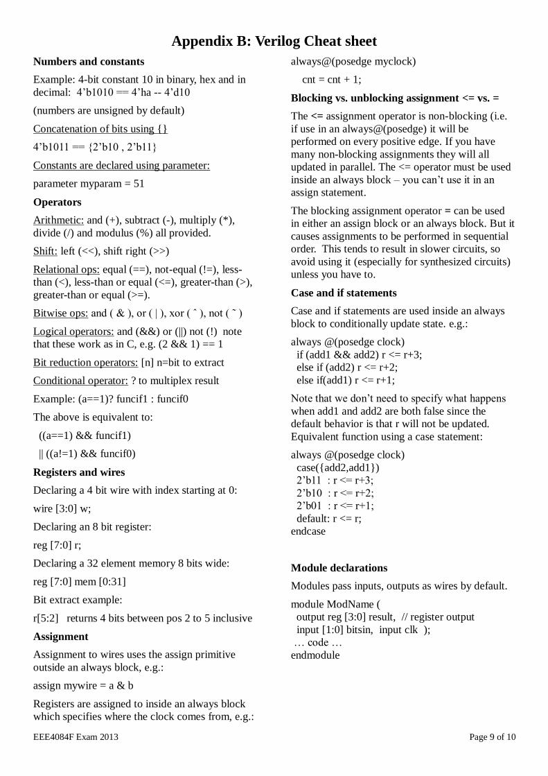
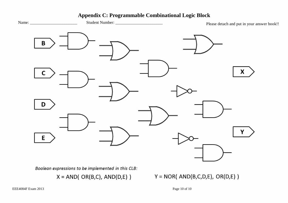
EEE4084F Exam 2013 Page 10 of 10
Appendix C Programmable Combinational Logic Block
Name _______________________ Student Number _______________________ Please detach and put in your answer book


