Embed Size (px)
Citation preview

Dimensioning of Ultra-Compact and Efficiency Power
Electronics Featuring Active Pulsating Power Buffer
for On-board EV Chargers
Shiyu Feng

Dimensioning of Ultra-Compact and Efficiency
Power Electronics Featuring Active Pulsating Power
Buffer for On-board EV Chargers
MASTER OF SCIENCE THESIS
For obtaining the degree of Master of Science in Electrical Engineering at Delft University of Technology
Shiyu Feng
April 2020
Supervisor: Dr.ir. Thiago Batista Soeiro Thesis Committee: Dr.ir. Thiago Batista Soeiro DCE&S, TU Delft Prof.dr. P. Bauer DCE&S, TU Delft
Dr. Alex Stefanov IEPG, TU Delft
An electronic version of this thesis is available at http://repository.tudelft.nl/

I
Abstract The Electric Vehicle (EV) charging market is very dynamic. The so-called AC-type chargers can be found confined within the vehicle or on-board. This must be able to withstand the harsh environment with an ambient temperature of above 75℃. Therefore, compact and high-efficiency power electronics and implementing electrolytic-less capacitors in the power range of 6 kW to 12 kW is desired. The operation of the grid-connected power stage with DC active power buffer has become standard in high compact systems. More importantly, this solution eliminates the requirement of high energy storage in the DC-link because the pulsating power is compensated leading to an electrolytic-less capacitor design. As the lifetime of the power converter in high-temperature environments is typically limited by the usage of the electrolytic capacitor technology, a more reliable system is finally obtained with the active pulsating power buffer.

II
Acknowledgements This thesis has been accomplished during the past year. It brought me great knowledge of electrical vehicles and valuable experience in simulation. I cannot finish it without the help of the following people, I would express my sincere appreciations to them. Firstly, I would like to thank my supervisor Dr. Thiago Batista Soeiro for his constant support and patient guidance. Secondly, I would like to thank Yang Wu, who helped me a lot and pushed me to go on in the latter half-year. Finally, I have to express my sincere gratitude to my parents. Thanks for supporting me all the time. It is your mental support that encouraged me to get through the hard time. Also, thanks to all my friends who brought me happiness in Delft.
III
Contents
ABSTRACT ...................................................................................................................................................... I
ACKNOWLEDGEMENTS ............................................................................................................................. II
CONTENTS ................................................................................................................................................... III
LIST OF FIGURES ......................................................................................................................................... V
LIST OF TABLES ....................................................................................................................................... VIII
LIST OF ACRONYMS ................................................................................................................................. IX
LIST OF SYMBOLS ....................................................................................................................................... X
1. INTRODUCTION ................................................................................................................................. 1
1.1 THESIS STRUCTURE .............................................................................................................................................. 3
2. BACKGROUND .................................................................................................................................... 4
2.1 SOCIETAL INSIGHTS OF ELECTRICAL VEHICLES ................................................................................................... 5 2.1.1 Electrical Vehicle Market ..................................................................................................................... 5 2.1.2 Advantages and disadvantages ............................................................................................................ 7
2.1 EV CHARGING POWER LEVELS ........................................................................................................................... 8 2.2.1 Level 1 Charging ..................................................................................................................................... 9 2.2.2 Level 2 Charging ................................................................................................................................... 10 2.2.3 Level 3 Charging ................................................................................................................................... 10
3. ELECTRONIC CAPACITOR TECHNOLOGIES ............................................................................... 12
3.1 ALUMINUM ELECTROLYTIC CAPACITORS ......................................................................................................... 14 3.2 TANTALUM ELECTROLYTIC CAPACITORS .......................................................................................................... 15 3.3 FILM CAPACITORS ............................................................................................................................................. 15
4. ON-BOARD CHARGING TECHNOLOGY ..................................................................................... 17
4.1 CHALLENGE ........................................................................................................................................................ 19
IV
4.2 APD CIRCUIT TOPOLOGIES .............................................................................................................................. 20 4.2.1 Full-bridge buck- and boost-type decoupling cells ....................................................................... 22 4.2.2 Half-bridge buck-type decoupling cells ........................................................................................... 24 4.2.3 Half-bridge boost-type decoupling cell ............................................................................................ 24 4.2.4 Half-bridge buck-boost-type decoupling cell .................................................................................. 25 4.2.5 Split capacitor decoupling port ......................................................................................................... 26
5. ACTIVE POWER DECOUPLING ...................................................................................................... 28
5.1 CHARGING SYSTEM WITH PASSIVE DECOUPLING DESIGN .............................................................................. 29 5.2 BUCK-TYPE DECOUPLING CELL DESIGN .......................................................................................................... 31
5.2.1 System Power Distribution ................................................................................................................. 31 5.2.2 Active Power Decoupling Capacitor Design .................................................................................. 33 5.2.3 Active Power Decoupling Inductor Design ..................................................................................... 35
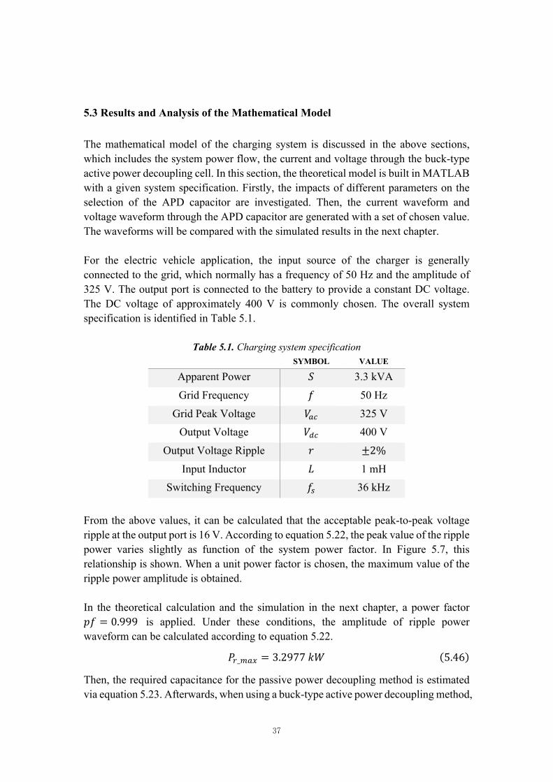
5.3 RESULTS AND ANALYSIS OF THE MATHEMATICAL MODEL ............................................................................. 37
6. SIMULATION AND ANALYSIS ....................................................................................................... 46
6.1 SIMULINK MODEL .............................................................................................................................................. 46 6.1.1 Rectifier PWM Control Algorithm .................................................................................................... 47 6.1.2 APD Circuit Control Algorithm ......................................................................................................... 50
6.2 RESULTS AND ANALYSIS ................................................................................................................................... 51
7. SYSTEM ELEMENTS COMPARISON ............................................................................................. 56
8. CONCLUSION AND FUTURE WORK ............................................................................................ 61
8.1 CONCLUSION ..................................................................................................................................................... 61 8.2 FUTURE WORK ................................................................................................................................................... 62
REFERENCE ................................................................................................................................................. 63
APPENDIX A ............................................................................................................................................... 68
APPENDIX B ............................................................................................................................................... 69
V
List of Figures
Figure 1.1. Conventional battery electrical vehicle: the Nissan Leaf ......................................... 1
Figure 2.1. Global EV sales for the past decade ......................................................................... 5
Figure 2.2. EV sales growth rate of five main countries ............................................................ 6
Figure 2.3. AC charging system and DC charging system… ..................................................... 9
Figure 2.4. The Level 1 onboard charger cord set in USA ...................................................... 10
Figure 2.5. The EVES for Level 2 Charging ............................................................................ 10
Figure 2.6. DC fast-charge station for Level 3 charging .......................................................... 11
Figure 3.1. Capacitor construction ............................................................................................ 13
Figure 3.2. Different types of electronic capacitors .................................................................. 13
Figure 3.3. Construction of an electrolytic capacitor ................................................................ 14
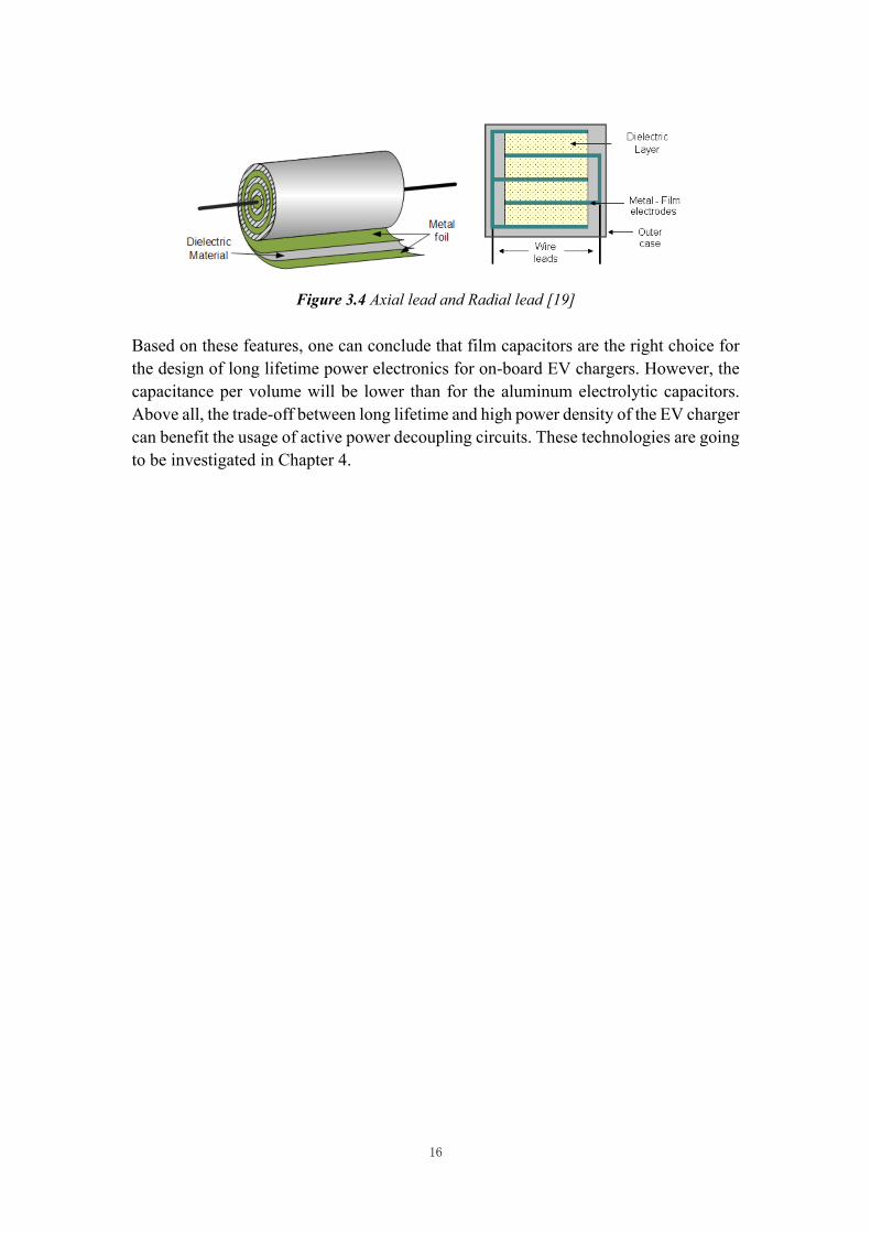
Figure 3.4. Axial lead and Radial lead .................................................................................... 16
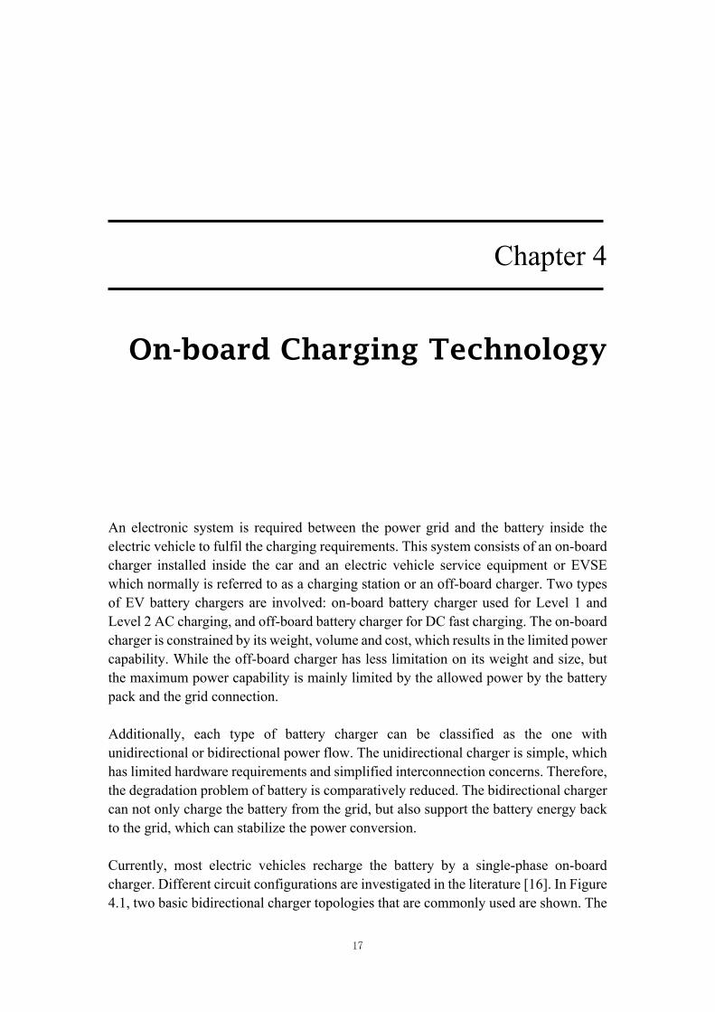
Figure 4.1. Bidirectional chargers: (a) single-phase half-bridge .............................................. 18
Figure 4.1. (b) single-phase full-bridge ........................................................................... 18
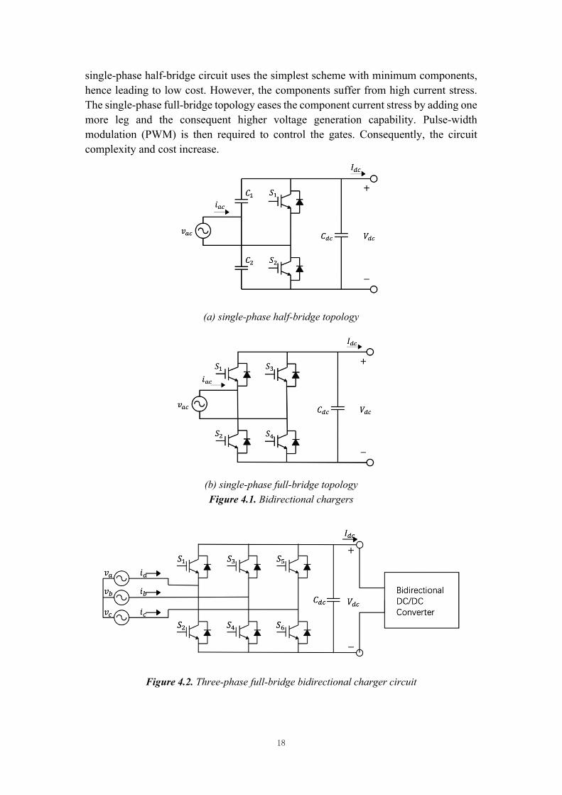
Figure 4.2. Three-phase full-bridge bidirectional charger circuit ............................................. 18
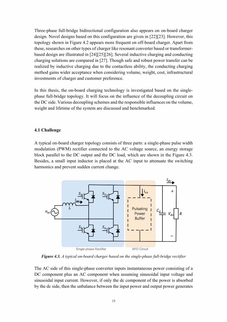
Figure 4.3. A typical on-board charger based on the single-phase full-bridge rectifier ........... 19
Figure 4.4. Full-bridge buck-type decoupling cell ................................................................... 22
Figure 4.5. Waveforms of voltage, current and power through circuit (Figure 4.4) ................ 22
Figure 4.6. Full-bridge boost-type decoupling cell ................................................................... 23
Figure 4.7. Waveforms of voltage, current and power through circuit (figure 4.6) ................. 23
Figure 4.8. Half-bridge buck-type decoupling cell ................................................................... 24
VI
Figure 4.9. Half-bridge boost-type decoupling cell .................................................................. 25
Figure 4.10. Half-bridge buck-boost type decoupling cell ....................................................... 25
Figure 4.11. Split capacitor decoupling cell ............................................................................. 26
Figure 4.12. Waveforms of capacitor voltages and DC voltage through decoupling circuit (Figure 4.11) ............................................................................................................................ 27
Figure 5.1. A typical front-end circuit of an on-board charger based on the single-phase full-bridge rectifier ........................................................................................................................... 28
Figure 5.2. Power distribution of the system with passive power decoupling ......................... 29
Figure 5.3. Power distribution of the system with active power decoupling ............................ 31
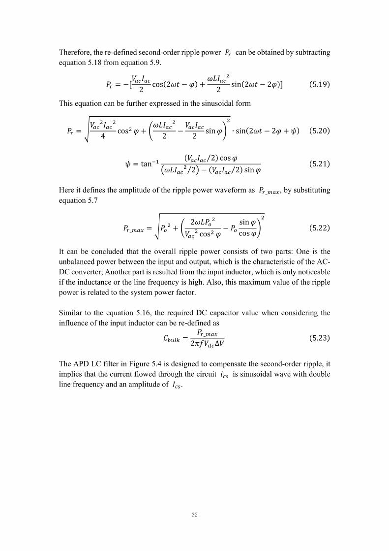
Figure 5.4. Buck-type active power decoupling circuit ............................................................ 33
Figure 5.5. instantaneous current flows through APD inductor ............................................... 35
Figure 5.6. voltage and current of APD inductor during one switching period ..................... 36
Figure 5.7. Relation between system power factor and peak ripple power .............................. 38
Figure 5.8. (a) Influence of K value on the capacitor voltage .................................................. 39
Figure 5.8. (b) Influence of K value on the capacitor voltage in 3D ........................................ 39
Figure 5.9. (a) Influence of K value on the capacitor current ................................................... 40
Figure 5.9. (b) Influence of K value on the capacitor current in 3D ........................................ 40
Figure 5.10. (a) Influence of C#$ value on the capacitor voltage ............................................ 41
Figure 5.10. (b) Influence of C#$ value on the capacitor voltage in 3D .................................. 41
Figure 5.11. (a) Influence of C#$ value on the capacitor current ............................................ 42
Figure 5.11. (b) Influence of C#$ value on the capacitor current in 3D .................................. 42
Figure 5.12. APD circuit current waveform ............................................................................. 43
Figure 5.13. Influence of M value on APD circuit voltage waveform ..................................... 44
Figure 5.14. Influence of C#$ value on APD circuit voltage waveform ................................. 44
Figure 6.1. Simulink model ...................................................................................................... 47
Figure 6.2. Rectifier control block diagram ............................................................................ 48
Figure 6.3. (a) Simulation results of rectifier PWM control ..................................................... 49
Figure 6.3. (b) Switching states of switches S1-S4 .................................................................. 49
Figure 6.3. (c) Zoom-in view of (a) .......................................................................................... 49
Figure 6.4. Active power decoupling control block diagram ................................................... 50
Figure 6.5. (a) Simulation results of APD circuit control ......................................................... 51
Figure 6.5. (b) Zoom-in view of (a) .......................................................................................... 51
Figure 6.6. Theoretical results of APD capacitor voltage and current ................................... 52

VII
Figure 6.7. Simulation results of APD capacitor voltage and current .................................... 53
Figure 6.8. Comparison between the measured capacitor current and the reference signal ..... 53
Figure 6.9. focus view on the peak current area ....................................................................... 53
Figure 6.10. Simulation result of output dc voltage ................................................................. 54
Figure 6.11. FFT analysis of ripple power ................................................................................ 55 Figure 7.1. APD current waveforms when 70% current ripple allowed ................................... 58
Figure 7.2. Inductor characteristics curve ..................................................................... 59
Figure 7.3. Inductor dimensions .................................................................................... 59

VIII
List of Tables
Table 5.1. Charging system specification ................................................................................. 37
Table 6.1. Switching states of PWM rectifier controller .......................................................... 48
Table 6.2. Switching states of APD controller .......................................................................... 50
Table 7.1. Results comparison for fixed dc capacitor value ..................................................... 56
Table 7.2. Results comparison for fixed M value ..................................................................... 57
Table 7.3. Results comparison for APD inductor ..................................................................... 57
Table 7.4. Passive components set for volume comparison ..................................................... 58
Table 7.5. Overall volume comparison ..................................................................................... 60
IX
List of Acronyms
1. EV Electric Vehicle
2. BEV Battery Electric Vehicle
3. PFC Power Factor Correction
4. APD Active Power Decoupling
5. PHEV Plug-In Hybrid Vehicle
6. VDC Vehicle Dynamics Control
7. 4WS Wheel Steering System
8. 4WD Four-Wheel Drive
9. EVES Electric Vehicle Supply Equipment
10. SAE Society of Automotive Engineers
11. IWC Infrastructure Working Council
12. OBC On-Board Charger
13. PWM Pulse-Width Modulation
14. ESR Effective Series Resistance
15. ESL Effective Series Inductance
16. VSC Voltage-Source Converter
17. CSC Current-Source Converter
18. BCM Boundary Conduction Mode
19. CCM Continuous Conduction Mode
20. DCM Discontinuous Conduction Mode
X
List of Symbols
𝜔 The fundamental line angular frequency
𝜑 The phase difference of input voltage and current
𝐴()*+ The volume for a single DC-link capacitor in passive decoupling
𝐴, The volume for a single APD capacitor
𝐴-,. The volume for a single fixed inductor for APD
𝐶()*+ The DC-link capacitor when passive decoupling applied
𝐶,. The APD capacitor
𝐶,.0 The upper capacitor in split capacitor decoupling cell
𝐶,.1 The lower capacitor in split capacitor decoupling cell
𝐶,._345 The minimal value required for APD capacitor
𝐶6 The DC-link capacitor when active decoupling applied
𝐸8 Ripple energy
𝐸,._39: Maximal energy storage of APD capacitor
𝑓 System line frequency
𝑓<5 The lower triangular modulation wave for PWM control
𝑓=, The triangular modulation wave for APD control
𝑓>? The upper triangular modulation wave for PWM control
𝑓. Switching frequency
𝑖9, Input AC current
𝐼9, Amplitude of input AC current
XI
𝑖, The current flows through DC-link capacitor
𝑖,. The current flows through APD capacitor
𝐼6, The DC output current
𝐾 Energy margin coefficient
𝐿 Input inductor
𝐿,. Inductor in APD circuit
𝑀 Average APD capacitor voltage defined
𝑃9, Input AC power
𝑃- Instantaneous power across input inductor
𝑃F Output power
𝑃8 Ripple power
𝑃8_39: Amplitude of ripple power defined
𝑟 Output voltage ripple allowance
𝑆 Apparent power
𝑢,J8* Reference control voltage generated for PWM control
𝑢,J8*_K, Reference control voltage generated for APD control
𝑢,. Instantaneous voltage across APD capacitor
𝑢,.0 Voltage of upper capacitor in split capacitor decoupling cell
𝑢,.1 Voltage of lower capacitor in split capacitor decoupling cell
𝑢- Instantaneous voltage across APD inductor
𝑣9, Input AC voltage
𝑉9, Amplitude of input AC voltage
𝑣, Voltage across DC-link capacitor in passive decoupling method
Vdc DC-link voltage
∆𝑉 Output voltage ripple
∆𝑖-. Current ripple

XII
1
Chapter 1
Introduction
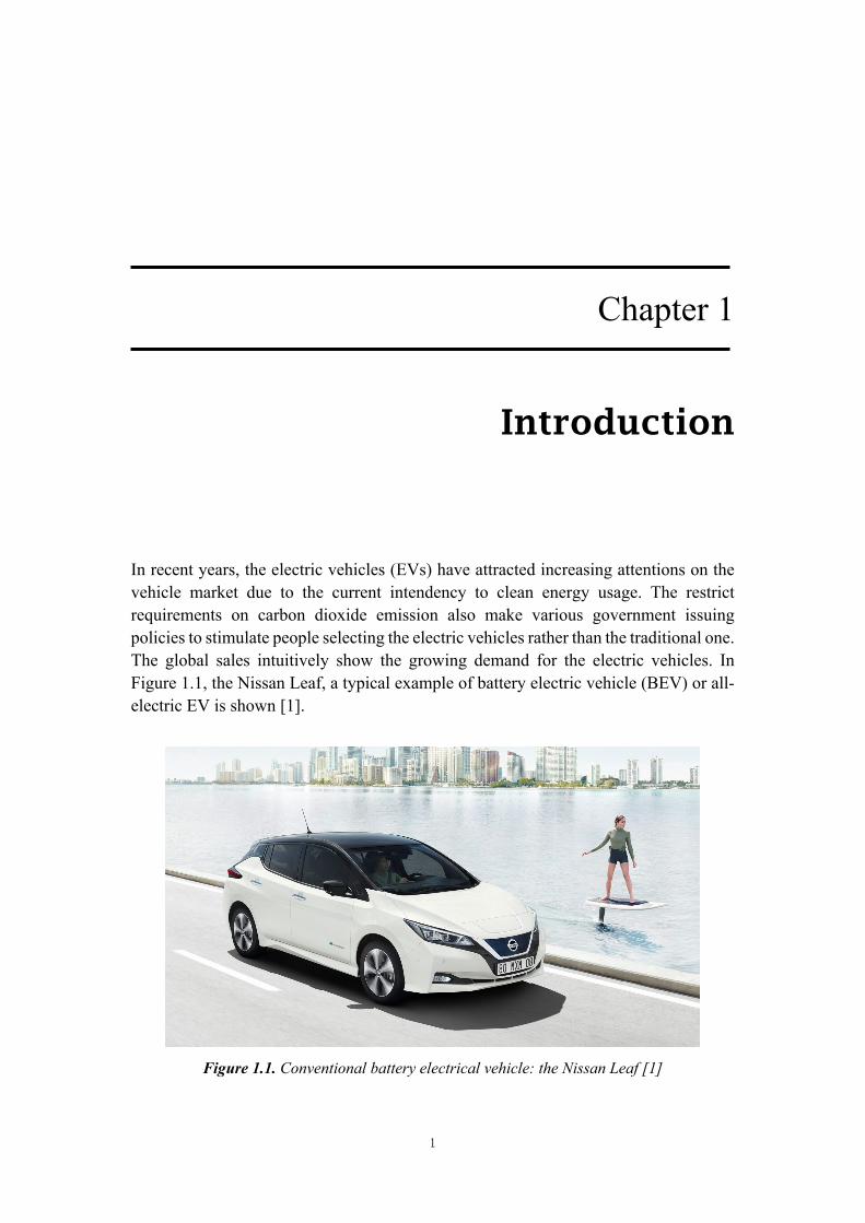
In recent years, the electric vehicles (EVs) have attracted increasing attentions on the vehicle market due to the current intendency to clean energy usage. The restrict requirements on carbon dioxide emission also make various government issuing policies to stimulate people selecting the electric vehicles rather than the traditional one. The global sales intuitively show the growing demand for the electric vehicles. In Figure 1.1, the Nissan Leaf, a typical example of battery electric vehicle (BEV) or all-electric EV is shown [1].
Figure 1.1. Conventional battery electrical vehicle: the Nissan Leaf [1]
2
With respect to the charging technology, the battery of the EVs can be fed by AC- or DC-type chargers [2]. The main difference between them is found on the power capability of the charging circuitry. AC-type chargers are located on-board the EV and have a power capability typically below 22 kW, while DC chargers are placed off-board the EV and can supply a wide range of power, e.g. from 11 kW to up to 350 kW, directly to the batteries. In Europe the AC-type level 1 chargers are found on-board the vehicle with a power capability below 7.4 kW. The power electronics is typically single-phase connected to the European grid, ua = 230V rms phase-to-neutral, where conventionally a multi-conversion stage system is employed. Therein, the front-end circuit provides power factor correction (PFC) operation to fulfil grid harmonic standards, while the required galvanic isolation from the grid is enabled at all time by the back-end converter. This thesis study will focus on the front-end circuit of an AC-type level 1 charger. One of the main challenges found on the design of this circuit is to attain long lifetime and reduced volume of the necessary DC-link capacitor interfacing the isolated back-end DC-DC converter. One effective solution for this is to apply a DC active power decoupling (APD) circuit to absorb the large pulsating power naturally observed in single-phase rectifiers. The APD together with long-life MKP film capacitors would be used as replacement of the commonly employed DC electrolytic capacitor. In this thesis, the research will focus mainly on the buck-type active power decoupling circuit. The software used for the mathematical analysis and simulation is MATLAB. The main objectives are shown as below: Ø Investigation on the social insight of the EV market.
Ø Literature review on different EV charging technologies, diverse active power
decoupling methods and the technologies of several possible capacitors.
Ø Construct the theoretical model based on half-bridge buck-type APD. Ø Build the simulation model in Simulink to match the theoretical results. Design the
control blocks for the simulation model. Ø Trade-off the selection of inductor and capacitor values. Define how parameters
selection affect the result. And finally, to select appropriate passive components and made volume comparison.
3
1.1 Thesis structure The contents of this thesis are organized as follow: Chapter 1 indicates the motivation and objectives of the thesis. The thesis structure is then listed with a brief summary. Chapter 2 investigates the current global electrical vehicle market. The development trend is analyzed. Advantages and disadvantages of EVs are discussed. Also, the potential improvement points are indicated. Then, three EV charging power levels are studied. Chapter 3 describes several capacitor technologies. The electrolytic capacitor used for passive power decoupling and the film capacitor used for active power decoupling circuit are discussed in detail. Chapter 4 firstly illustrates the commonly used circuit topologies for front-end circuit for on-board and off-board chargers. Then, it will focus on the front-end circuit of the on-board charging technology. The main challenge for the studied single-phase voltage source rectifier stage is proposed. Five frequently used active power decoupling circuits are discussed. Chapter 5 studies the buck-type power decoupling circuit. The power flow of a single-phase AC-DC voltage source converter is analytically derived for both passive filtering and active power decoupling methods. The influences of several factors on the components selection and design for a specific system are explored. Chapter 6 introduces the developed simulation model and the correspond feedback control loop methods. The simulation results for the specific system are plotted and compared with the developed theoretical method. Chapter 7 gives the conclusion for the thesis. Several future studies are suggested.
4
Chapter 2
Background
The electrical vehicles (EVs) represent any vehicle that uses electric energy taken from the power grid and stored on-board in the battery for the propulsion. According to the fuel type, EVs can be classified into plug-in hybrid vehicles (PHEVs) which have both battery and internal combustion engine and battery electric vehicles (BEVs) which use pure electricity. The vehicle electrification provides a pathway for decarbonization, which contributes to the low carbon dioxide emission and better air quality. Also, the electrical vehicle benefits from its simple structure, high energy utilization rate and low noise. However, today the EVs market is restricted by the current high price, typical larger size and weight and the long charging time of the battery pack. The electrical vehicle has been commercially available in the global market in the recent decade. It gradually became one popular choice. The growing success of electrical vehicles is mainly attributed to the rapidly improving energy storage technology and also to the globally adopted incentive policies. In this chapter, the background information and societal insights of EVs are reviewed. Then, the charging modes of the EVs are discussed. Finally, several charging standards are discussed.
5
2.1 Societal Insights of Electrical Vehicles
2.1.1 Electrical Vehicle Market
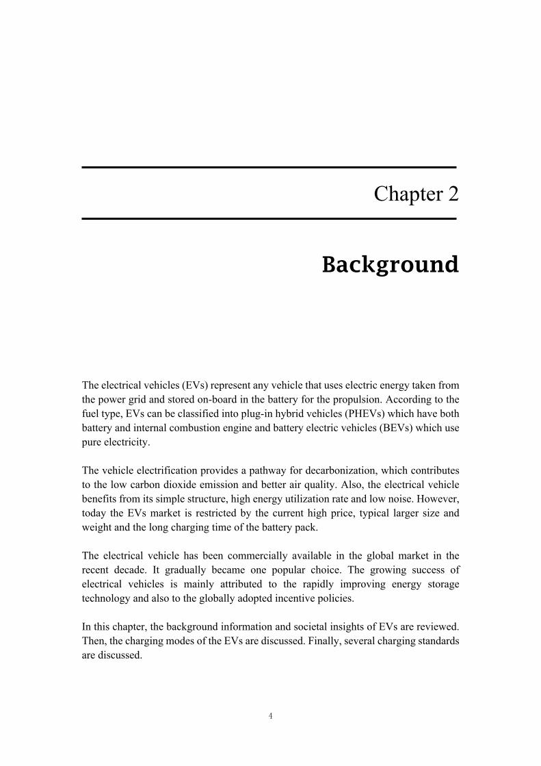
Over the past 10 years, there has been a rapid growth in the development of the electric cars. It can be witnessed that electric mobility is expanding at a rapid pace. According to the Global EV Outlook 2019, more than 5.1 million total electric cars have been reached worldwide in 2018, including both PHEVs and BEVs [2]. This is a 2 million increase compared to 2017, which is an enormous escalation of approximately 64%. The global sales growth for all PHEVs and BEVs from the previous decade can be clearly perceived from Figure 2.1 [3]. The blue bar indicates the total global sales for each year, while the yellow line shows the year over year growth rate. The electric vehicles expanded at a rate of 46% to 69% through the years. However, focused on the global light vehicle market, the electric vehicles only share a small part. According to [3], only 2.2 percent of the vehicles run based on electricity in the world. As for 2019, this proportion was 3.5 percent in June and 2.5 percent for the first half-year [4]. Therefore, it suggests that there is a long way to go to realize the electrification for vehicle transport. Considering the overall EV sales in the first half of 2019, BEV occupied 74 percent, while the rest proportion is PHEV. This distribution shifts 11% to the BEVs compared to the same period of 2018 [4]. Higher demand for all-electric EVs can be indicated.
Figure 2.1. Global EV sales for the past decade [3]
The growing market for EVs, especially the all-electric ones is influenced by several factors: The policies introduced by the governments of several countries, the stringent
6
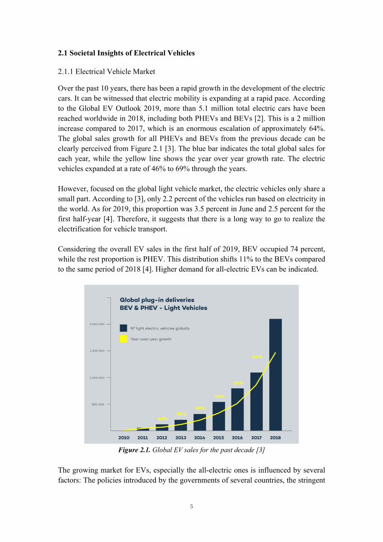
light vehicle test procedure for carbon dioxide and the technical breakthrough in the new-released car models. Several articles stated and analyzed that the policies are of great significance in incentives for electric vehicles implementation. The top three largest electric car markets of the world are China, Europe and the United States. Among them, China not only keeps the largest EV market during recent years, but also behaves as the largest growth contributor. An example of the growth rate of the main EV markets from 2018 to 2019 can be shown in Figure 2.2 [4]. Wenbo illustrated that China has delivered numerous policies to assist this high adoption rate, which covers seven aspects. While macroscopic, subsidization, tax and technical support played a vital role in the development [5]. A complex model built by Gillian provides further understanding of the interaction between the policies and the transition towards e-mobility [6]. Norway is always the leader in the global electric vehicle market share. Norwegian owners emphasized the importance of the policy incentives, which evidently reduced both purchase and usage costs [7]. Similarly, the stimulated policies issued by different governments correspondingly show significant influence on the US, Japan, UK and other European EV markets [8][9].
Figure 2.2. EV sales growth rate of five main countries. [4]
The Europe introduction of severe 𝐶𝑂1 test procedures was reflected by the increase ratio of the EV sold. It results in the higher BEV share and slightly reduced PHEV share in the EU market. The European Union was committed to reduce greenhouse gas emission by 40% and reduce 60% of road transport emission compared to 1990 levels by 2030. Moreover, they aimed to halve the conventional car usage in the urban area by 2030[6]. Therefore, electric vehicles as zero-tailpipe transportation will gradually become the prior choice.
7
From Figure 2.2, the US market increased 23% in the first half of 2019. For the whole year, the increased percentage came to 89% [4]. This upsurge was attributed to the new released Tesla Model-3. The main competitive advantages of this model are the new battery technologies. The recently applied battery patent provides enhanced energy storage capability, condensed charging time and advanced energy density [10]. The technical advances including the improvement in the battery chemistry, enhancement of energy density and the size reduction of the battery packs will benefit the future EV market. All of these factors boost the global EV market. The future development will be profited by the following policies support, convenient charging infrastructure and improvements on charging technology.
2.1.2 Advantages and disadvantages
Compared to the conventional combustion engine vehicles, the electric vehicles have several advantages.
• Energy Consumption The global car stock is huge. From the point of view of the energy, there exists a severe shortage of petroleum consumption, especially for the fuel import countries. Alternative fuels like hydrogen, methane are preferable. The popularization of EVs can diversify the energy structure. The electricity from the grid can be generated from different energies like coal, solar, nuclear, wind and natural gas. So, it can diminish the shortage of non-renewable energy source. Also, the power transfer efficiency increase can also reduce the energy consumption.
• Air Quality From the environment aspect, the transportation emission is the main reason for the environment pollution and greenhouse gas emission. Generally, transport accounts for approximately one-third of energy-related 𝐶𝑂1 emission [11]. The use of EVs can reduce the pollutant emission containing 𝐶𝑂1, 𝑃𝑀1.R, 𝑁𝑂: and 𝑆𝑂1compared to the traditional vehicles [12]. As there is no tailpipe on the EVs, no emission is caused by themselves. Thus no air pollution will be generated. Though the EVs are clean, the electricity generated by the power plants may still cause pollution. However, this depends on the fuel sources used. When the clean source like solar energy or wind energy is used, the contamination is negligible. Based on the investigation of Jihu, 1.6 billion liters gasoline consumption and 611 hundred tons 𝐶𝑂1 emission were reduced in five major provinces in China from 2011 to 2017. And three-quarter reduction was donated by the BEVs [13]. Moreover, it is easier to control the contamination based on power plants than every single car. Consequently, better air quality can be achieved through the use of EVs.
• Performance
8
Compared to the vehicles with combustion engines, EVs have better controllability, stability and safety performance. The vehicle dynamics control (VDC) is widely applied to EVs, which helps control the moving status and increases the maneuverability. Apart from that, the use of wheel steering system (4WS) and four-wheel drive (4WD) improves the controlling performance. Also, the anti-lock braking system develops stability and safety. The electric engine can provide full torque from a standstill, which offers a better experience on a fast-moving highway. The quiet, smooth and powerful journey can be provided by EVs.
• Convenience There is no engine, transmission, spark plugs, valves, fuel tank, tailpipe, distributor, starter, cloth, muffler, or catalytic converter in the electric vehicles. The fewer car components result in lower maintenance costs compared to gasoline cars. Apart from that, it is convenient as that there is no need for service stations, tune-ups, transmission repairs or oil changes.
• Affordability The cost of subsidized electricity can be lower that of the gasoline price. Therefore, the price of charging an EV with electricity can be similar or even lower than fueling a car with gas. Also, the electricity prices are much more stable than the gasoline prices. The drivers may suffer less from the price risks. However, electric vehicles still have some limitations. The public charging points are still in the development stages, that means the usage EVs can be somewhat limited to some area. Due to short capacity of the batteries there are also restrictions on the driving distance and speed. Moreover, the high cost, long charging time and cycle life of batteries are sometimes inconvenient. This paper will focus on the improvement of the charging technology.
2.1 EV Charging Power Levels
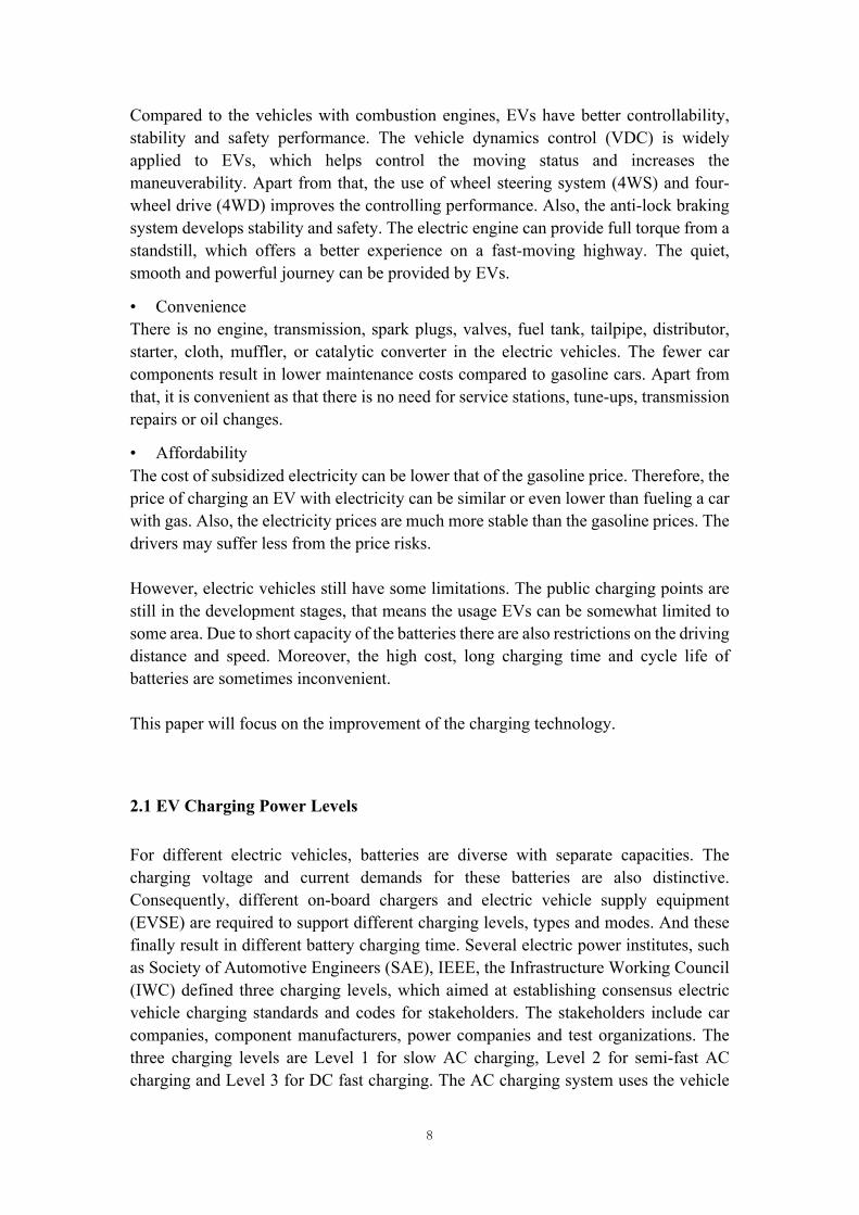
For different electric vehicles, batteries are diverse with separate capacities. The charging voltage and current demands for these batteries are also distinctive. Consequently, different on-board chargers and electric vehicle supply equipment (EVSE) are required to support different charging levels, types and modes. And these finally result in different battery charging time. Several electric power institutes, such as Society of Automotive Engineers (SAE), IEEE, the Infrastructure Working Council (IWC) defined three charging levels, which aimed at establishing consensus electric vehicle charging standards and codes for stakeholders. The stakeholders include car companies, component manufacturers, power companies and test organizations. The three charging levels are Level 1 for slow AC charging, Level 2 for semi-fast AC charging and Level 3 for DC fast charging. The AC charging system uses the vehicle
9
on-board charger (OBC) to charge the battery, while the DC charging system directly charges the battery from an off-board AC-DC power converter connected to the grid.
Figure 2.3. Power flow in AC charging system and DC charging system
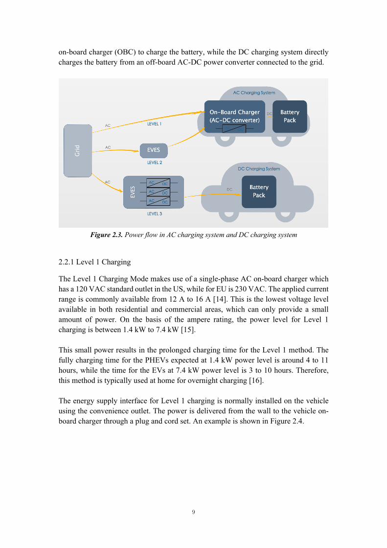
2.2.1 Level 1 Charging
The Level 1 Charging Mode makes use of a single-phase AC on-board charger which has a 120 VAC standard outlet in the US, while for EU is 230 VAC. The applied current range is commonly available from 12 A to 16 A [14]. This is the lowest voltage level available in both residential and commercial areas, which can only provide a small amount of power. On the basis of the ampere rating, the power level for Level 1 charging is between 1.4 kW to 7.4 kW [15]. This small power results in the prolonged charging time for the Level 1 method. The fully charging time for the PHEVs expected at 1.4 kW power level is around 4 to 11 hours, while the time for the EVs at 7.4 kW power level is 3 to 10 hours. Therefore, this method is typically used at home for overnight charging [16]. The energy supply interface for Level 1 charging is normally installed on the vehicle using the convenience outlet. The power is delivered from the wall to the vehicle on-board charger through a plug and cord set. An example is shown in Figure 2.4.
10
Figure 2.4 The Level 1 on-board charger cord set in USA [16]
2.2.2 Level 2 Charging
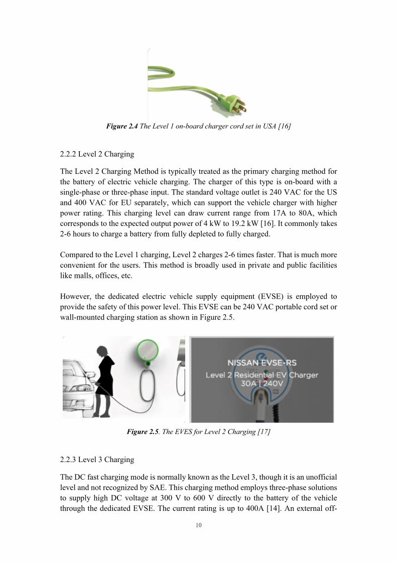
The Level 2 Charging Method is typically treated as the primary charging method for the battery of electric vehicle charging. The charger of this type is on-board with a single-phase or three-phase input. The standard voltage outlet is 240 VAC for the US and 400 VAC for EU separately, which can support the vehicle charger with higher power rating. This charging level can draw current range from 17A to 80A, which corresponds to the expected output power of 4 kW to 19.2 kW [16]. It commonly takes 2-6 hours to charge a battery from fully depleted to fully charged. Compared to the Level 1 charging, Level 2 charges 2-6 times faster. That is much more convenient for the users. This method is broadly used in private and public facilities like malls, offices, etc. However, the dedicated electric vehicle supply equipment (EVSE) is employed to provide the safety of this power level. This EVSE can be 240 VAC portable cord set or wall-mounted charging station as shown in Figure 2.5.
Figure 2.5. The EVES for Level 2 Charging [17]
2.2.3 Level 3 Charging
The DC fast charging mode is normally known as the Level 3, though it is an unofficial level and not recognized by SAE. This charging method employs three-phase solutions to supply high DC voltage at 300 V to 600 V directly to the battery of the vehicle through the dedicated EVSE. The current rating is up to 400A [14]. An external off-
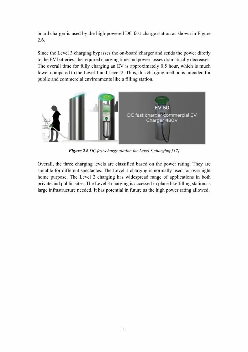
11
board charger is used by the high-powered DC fast-charge station as shown in Figure 2.6. Since the Level 3 charging bypasses the on-board charger and sends the power diretly to the EV batteries, the required charging time and power losses dramatically decreases. The overall time for fully charging an EV is approximately 0.5 hour, which is much lower compared to the Level 1 and Level 2. Thus, this charging method is intended for public and commercial environments like a filling station.
Figure 2.6 DC fast-charge station for Level 3 charging [17] Overall, the three charging levels are classified based on the power rating. They are suitable for different spectacles. The Level 1 charging is normally used for overnight home purpose. The Level 2 charging has widespread range of applications in both private and public sites. The Level 3 charging is accessed in place like filling station as large infrastructure needed. It has potential in future as the high power rating allowed.
12
Chapter 3
Electronic Capacitor
Technologies Electronic capacitors are used as the ripple energy storage component in the EV on-board charging system. In the application of the EV on-board charging, a single-phase pulse-width modulation (PWM) rectifier is utilized, which normally generates a second-order harmonic current at the DC-side and therefore ripple voltage in the DC load, which makes the output to vary from the idealized constant value. It is critical to use a circuit decoupling topology to minimize the negative influence of this ripple power. The minimum ripple energy requirement for a specific system is independent of the decoupling circuit. In the traditional applications, the passive decoupling method is applied, and a bulk capacitor is usually placed at the DC side. The usage of this capacitor leads to low power density and large volume of the power electronics. To achieve a better power density and consequently smaller volume of the circuit, several active decoupling topologies have been explored in different applications, which are discussed in the next chapter. These methods commonly make use of an auxiliary circuit comprising of semiconductors, inductors and capacitors. For the electric vehicle charging system, high power density is always required. Also, it is preferred to have a small converter volume. Thus, the characteristics and the volume and the lifetime of the capacitors used in the system are discussed in this chapter.
13
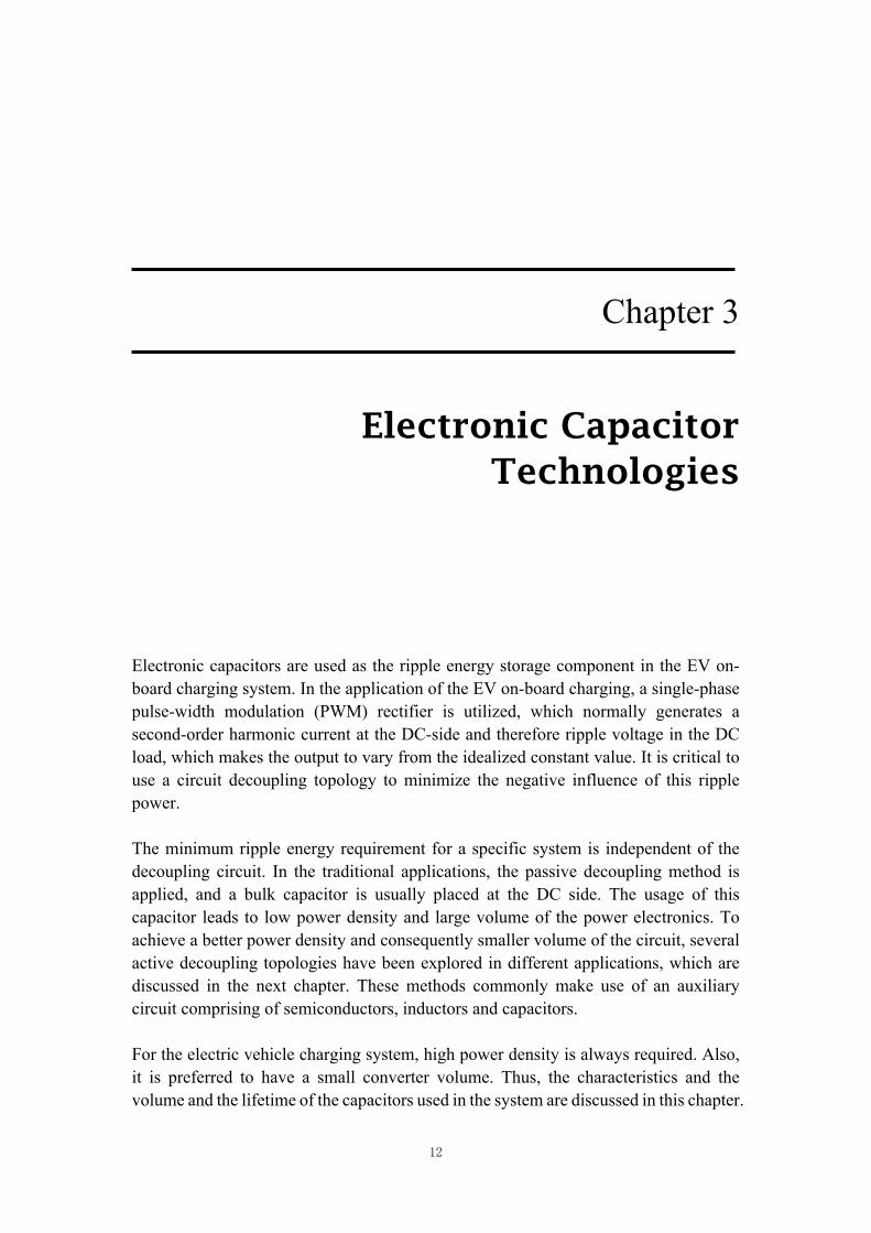
Figure 3.1 Capacitor construction
Capacitors can be manufactured in different techniques using different materials. However, they commonly have similar constructions of two or more parallel conductive plates not connected with each other and the insulating dielectric layer between the plates. The conductive plates can be different shapes such as rectangular, circular or cylindrical. The dielectric can be the air, ceramic, plastic or some kind of liquid, which electrically separate the conductive plates. Consequently, three factors are used to determine the capacitance: the permittivity 𝜖 of the dielectric, the conductive plates surface area A and the distance between the plates d.
𝐶 = 𝜖𝐴𝑑 (3.1)
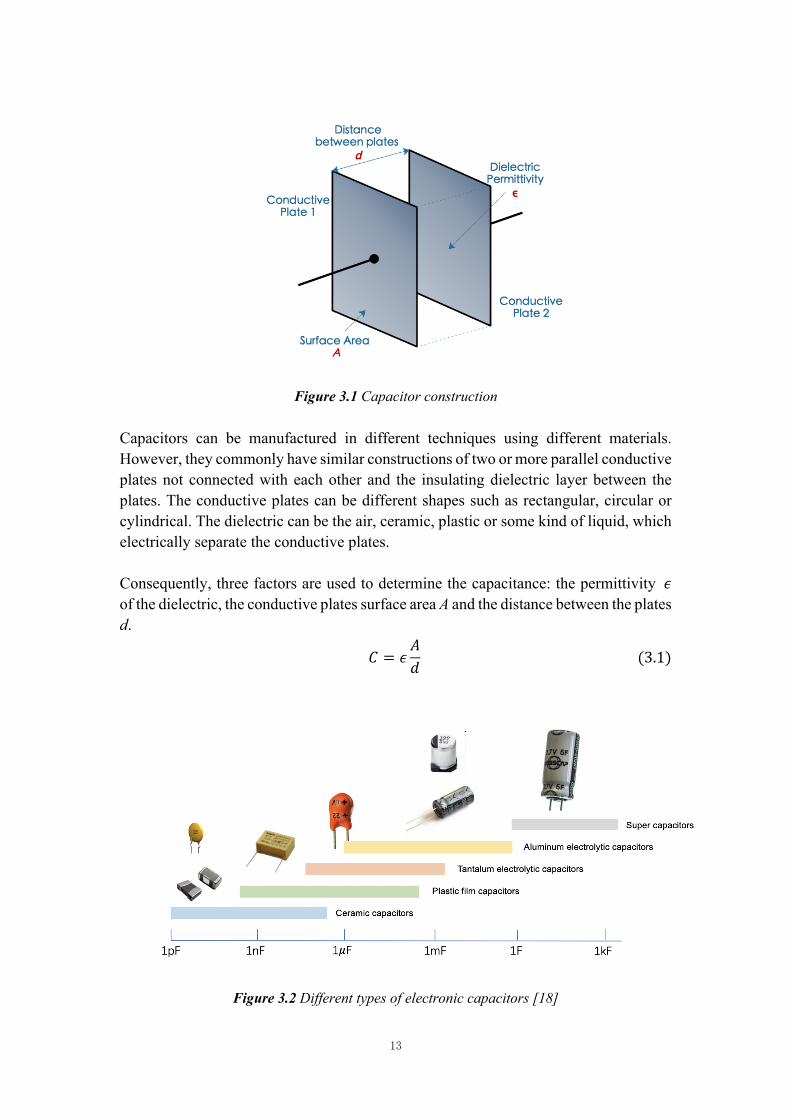
Figure 3.2 Different types of electronic capacitors [18]
14
From the Figure 3.2, it can be seen that there is a large variety of types of capacitor commonly available in the market, ranging from very small ceramic ones to large power factor correction capacitors. Each type of capacitors has its own benefits and drawbacks. The usual choices for the capacitors used in the DC-link as energy storage devices on EV charging system are electrolytic capacitors and film capacitors.
3.1 Aluminum Electrolytic Capacitors
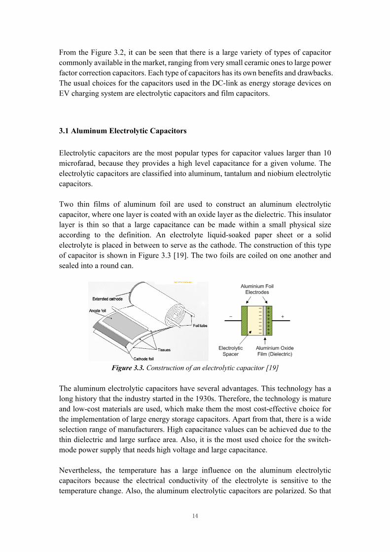
Electrolytic capacitors are the most popular types for capacitor values larger than 10 microfarad, because they provides a high level capacitance for a given volume. The electrolytic capacitors are classified into aluminum, tantalum and niobium electrolytic capacitors. Two thin films of aluminum foil are used to construct an aluminum electrolytic capacitor, where one layer is coated with an oxide layer as the dielectric. This insulator layer is thin so that a large capacitance can be made within a small physical size according to the definition. An electrolyte liquid-soaked paper sheet or a solid electrolyte is placed in between to serve as the cathode. The construction of this type of capacitor is shown in Figure 3.3 [19]. The two foils are coiled on one another and sealed into a round can.
Figure 3.3. Construction of an electrolytic capacitor [19]
The aluminum electrolytic capacitors have several advantages. This technology has a long history that the industry started in the 1930s. Therefore, the technology is mature and low-cost materials are used, which make them the most cost-effective choice for the implementation of large energy storage capacitors. Apart from that, there is a wide selection range of manufacturers. High capacitance values can be achieved due to the thin dielectric and large surface area. Also, it is the most used choice for the switch-mode power supply that needs high voltage and large capacitance. Nevertheless, the temperature has a large influence on the aluminum electrolytic capacitors because the electrical conductivity of the electrolyte is sensitive to the temperature change. Also, the aluminum electrolytic capacitors are polarized. So that
15
this kind of capacitors must be connected in the correct direction in the circuit. Besides, this capacitor type has large parasitic, where large effective series resistance (ESR) and large effective series inductance (ESL) exist [21]. Moreover, the electrolyte will eventually dry out, which severely limits the lifetime of the capacitors.
3.2 Tantalum Electrolytic Capacitors
The tantalum electrolytic capacitors have a similar construction as the aluminum one. The difference is that a tantalum film covered with the oxide layer is used as the dielectric. Compared to the aluminum one, this type has a much smaller size. It has a high capacitance per unit volume. This advantage is important for the applications that have strict limitation in size. Furthermore, it has relatively low ESR and low ESL. Also, several manufacturers are available for these capacitors.. However, the tantalum electrolytic capacitors have a limited working voltage range of 35 V maximum [18]. Thus, it can only be reliable for low operating voltage applications under 35 V. And similarly, the tantalum electrolytic capacitors are polarized.
3.3 Film Capacitors
Film capacitors are the most commonly used capacitors ranging from values as small as 5 pF to as large as 100uF depending on the actual type [19]. The film capacitors can be assorted based on the construction in the metallized film capacitors and film foil capacitors. Aluminum or zinc is used to make the electrodes of the capacitor. And a plastic film is placed in between the dielectric layer. A wide variety of dielectric properties like polystyrene, polycarbonate, polyester, polypropylene, metalized paper and Teflon can be selected. The construction can be radial or axial lead as shown in Figure 3.4. The film capacitors can also be classified into three groups according to their shapes and case styles: the wrap and fill one that is wrapped in tight plastic tape and sealed the ends with epoxy, the epoxy case one that is encased in molded plastic shell with epoxy filled in, and the metal hermetically sealed one that is encased in a metal tube. The plastic film capacitors have the advantages of the good high-temperature performance, the relatively small tolerance, the long service lifetime and the high stability compared to the impregnated-paper type [21]. Apart from that, film capacitors are normally non-polarized.
16
Figure 3.4 Axial lead and Radial lead [19]
Based on these features, one can conclude that film capacitors are the right choice for the design of long lifetime power electronics for on-board EV chargers. However, the capacitance per volume will be lower than for the aluminum electrolytic capacitors. Above all, the trade-off between long lifetime and high power density of the EV charger can benefit the usage of active power decoupling circuits. These technologies are going to be investigated in Chapter 4.
17
Chapter 4
On-board Charging Technology
An electronic system is required between the power grid and the battery inside the electric vehicle to fulfil the charging requirements. This system consists of an on-board charger installed inside the car and an electric vehicle service equipment or EVSE which normally is referred to as a charging station or an off-board charger. Two types of EV battery chargers are involved: on-board battery charger used for Level 1 and Level 2 AC charging, and off-board battery charger for DC fast charging. The on-board charger is constrained by its weight, volume and cost, which results in the limited power capability. While the off-board charger has less limitation on its weight and size, but the maximum power capability is mainly limited by the allowed power by the battery pack and the grid connection. Additionally, each type of battery charger can be classified as the one with unidirectional or bidirectional power flow. The unidirectional charger is simple, which has limited hardware requirements and simplified interconnection concerns. Therefore, the degradation problem of battery is comparatively reduced. The bidirectional charger can not only charge the battery from the grid, but also support the battery energy back to the grid, which can stabilize the power conversion. Currently, most electric vehicles recharge the battery by a single-phase on-board charger. Different circuit configurations are investigated in the literature [16]. In Figure 4.1, two basic bidirectional charger topologies that are commonly used are shown. The
18
single-phase half-bridge circuit uses the simplest scheme with minimum components, hence leading to low cost. However, the components suffer from high current stress. The single-phase full-bridge topology eases the component current stress by adding one more leg and the consequent higher voltage generation capability. Pulse-width modulation (PWM) is then required to control the gates. Consequently, the circuit complexity and cost increase.
(a) single-phase half-bridge topology
(b) single-phase full-bridge topology Figure 4.1. Bidirectional chargers
Figure 4.2. Three-phase full-bridge bidirectional charger circuit
19
Three-phase full-bridge bidirectional configuration also appears on on-board charger design. Novel designs based on this configuration are given in [22][23]. However, this topology shown in Figure 4.2 appears more frequent on off-board charger. Apart from these, researches on other types of charger like resonant converter based or transformer-based design are illustrated in [24][25][26]. Several inductive charging and conducting charging solutions are compared in [27]. Though safe and robust power transfer can be realized by inductive charging due to the contactless ability, the conducting charging method gains wider acceptance when considering volume, weight, cost, infrastructural investments of charger and customer preference. In this thesis, the on-board charging technology is investigated based on the single-phase full-bridge topology. It will focus on the influence of the decoupling circuit on the DC side. Various decoupling schemes and the responsible influences on the volume, weight and lifetime of the system are discussed and benchmarked.
4.1 Challenge
A typical on-board charger topology consists of three parts: a single-phase pulse width modulation (PWM) rectifier connected to the AC voltage source, an energy storage block parallel to the DC output and the DC load, which are shown in the Figure 4.3. Besides, a small input inductor is placed at the AC input to attenuate the switching harmonics and prevent sudden current change.
Figure 4.3. A typical on-board charger based on the single-phase full-bridge rectifier
The AC side of this single-phase converter inputs instantaneous power consisting of a DC component plus an AC component when assuming sinusoidal input voltage and sinusoidal input current. However, if only the dc component of the power is absorbed by the dc side, then the unbalance between the input power and output power generates
20
the inevitable second-order components on the DC bus. This power distinction is twice the line frequency and generally called pulsating power or ripple power, which risks the system operation. Consequently, a power decoupling circuit block is installed between the rectifier and DC load to diminish the voltage and current fluctuation. The most common way to limit the ripple is to parallel to the DC output a passive decoupling circuit, such as, a bulk DC-link capacitor or a DC-link inductor or a notch LC filter. The LC notch filter refers to a series inductor and capacitor branch that is designed to have the resonant frequency double the line frequency in order to absorb the ripple power [28]. These methods can be easily implemented. Nevertheless, large capacitances are required for the passive decoupling systems, which leads to capacitors with massive volume and weight, especially for the high voltage and high-power applications like onboard electric vehicles. This will result in low power density and is undesirable in practice. Apart from that, as discussed in Chapter 3, aluminum electrolytic capacitors are the usual choice for large capacitance, which has the drawback of a limited lifetime. Reliability problem and maintenance costs will increase. Therefore, it is expected to have an alternative approach to achieve high power density, longer lifetime, better reliability and low cost. In recent years, active power decoupling methods have been frequently investigated to eliminate the aforementioned shortcomings. The active decoupling technique consists of two parts: the control algorithms and the decoupling circuit topologies. By monitoring the state of the switches, the ripple power is actively channeled away from the DC port to the energy storage devices. The voltage of this part can be tuned independently of the load voltage. Thus, the time-varying decoupling voltage and current can change to match the ripple power. Since this, the capability of the energy storage element can be effectively used, which allows a smaller capacitance compared to the passive DC capacitor. The active decoupling method benefits from the use of more reliable film capacitors. And the reducing size and weight are essential for the volume-critical and weight-critical electric vehicles. Nonetheless, the main drawback of this method is the import of extra components and the control system, which is necessary to analyze and the trade-off between the increased power density and the added complexity.
4.2 APD Circuit Topologies Various researches have been carried out on active power decoupling. Depending on the applications at hand, different circuit topologies and control methods are employed. Diverse categories are used to classify these active power decoupling methods.
• Control circuit topology One commonly used classification is based on the type of the control circuit used to drive the active power decoupling block. The decoupling control circuit can be
21
implemented with or without sharing the main switches of the single-phase rectifier. Thus, the first category is the independent power decoupling circuit (IPDC) where both the switches and the energy storage elements are additionally self-controlled. This topology is flexible to control. The second category is the dependent power decoupling circuit (DPDC), which uses one shared switches leg to realize both power conversion and power decoupling. This type of topology has the advantage of fewer components, reduced cost and volume. However, more complexity is caused owing to the coupling between the control of the decoupling circuit leg and rectifier leg.
• Energy storage element Two primary energy storage elements are usually implemented in the active power decoupling circuit: inductors and capacitors. The capacitive energy storage element stores the ripple energy in the electrostatic field of capacitors, while the inductive one saves the ripple energy in the inductor electromagnetic field. Compared to the inductors, capacitors draw more attention due to the higher energy per volume and cost reason. Apart from that, the inductors have comparable high ESR, which dramatically reduce the system efficiency. And the non-linear characteristics of inductors make it more complicated its proper selection and over dimensioning can be the result.
• Control method The control strategies can be classified into the open-loop and the closed-loop control methods. The closed-loop method is frequently chosen, which makes use of the feedback loop from the output to adjust the compensation parameter. The reference signals of the power decoupling system are various, which can be the ripple voltage, ripple current, AC voltage, AC current or their combination.
• Topology structure From the topology standpoint, different decoupling circuit cells have been applied in different studies, such as the H-bridge type, buck type, boost type, buck-boost type. Each decoupling cell can be connected in series or in parallel with the main converter. Furthermore, multistage active circuits are sometimes implemented rather than single-stage circuits. According to [29], the basic power decoupling cells can be classified into voltage-source oriented type and current-source-oriented type. This is decided by the voltage-source converter (VSC) or current-source converter (CSC) the decoupling cells are connected to. Each category can be further divided through the above categories. On the following, a general overview of several basic power decoupling circuits based on voltage-source converters which uses capacitors as the main storage element is provided and discussed in detail.
22
4.2.1 Full-bridge buck- and boost-type decoupling cells
A full bridge circuit is the most direct way to construct an independent control adjusting the sinusoidal voltage and current to the energy storage element. The full bridge decoupling cell consists of four switches and an LC circuit connected between. The Figure 4.4 shows the configuration with defined DC terminal voltage and alternative capacitor voltage. The capacitor stores the ripple energy, while a small inductor is implemented to guarantee a smoother current. The on/off state of the switches are controlled to match the ripple power. The capacitor stores the energy when the input AC power is positive, while the capacitor releases the energy to the load as the input power is negative.
Figure 4.4. Full-bridge buck-type decoupling cell The waveforms of the ideal sinusoidal voltage and current input to the decoupling circuit and the resulting ripple power are indicated in Figure 4.5. The control system is expected to be designed directly to track the ripple power of the main rectifier circuit. However, it is commonly designed indirectly to refer to the expected capacitor voltage or current, and then to match the calculated capacitor power to the ripple power.
Figure 4.5. Waveforms of voltage, current and power through decoupling circuit (Figure 4.4)
23
This buck-type decoupling circuit has the limitation of restricted capacitor voltage, ucs, which should be lower than the DC-link voltage, Vdc. This restriction is generally accepted due to the safety consideration. However, a higher capacitor voltage is needed to have further capacitance reduction in some applications. Another full-bridge decoupling circuit configuration shown in Figure 4.6 can withstand a capacitor voltage higher than the DC voltage because the structure is a boost-type circuit. Its corresponding waveforms can be seen in Figure 4.7.
Figure 4.6. Full-bridge boost-type decoupling cell.
Figure 4.7. Waveforms of voltage, current and power through decoupling circuit (Figure 4.6)
This type of decoupling port suffers from relatively high voltage stress, while the capacitance needed is relatively small compared to the buck-type circuit depicted in Figure 4.4.
24
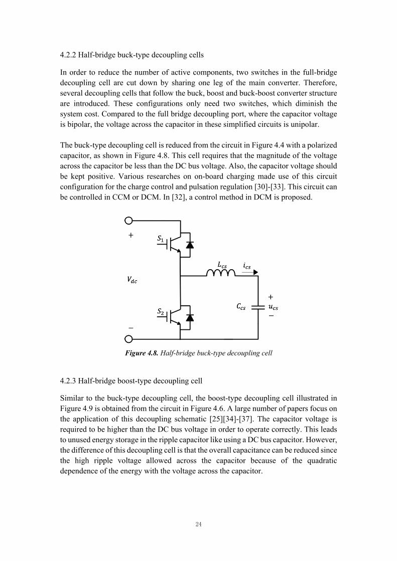
4.2.2 Half-bridge buck-type decoupling cells
In order to reduce the number of active components, two switches in the full-bridge decoupling cell are cut down by sharing one leg of the main converter. Therefore, several decoupling cells that follow the buck, boost and buck-boost converter structure are introduced. These configurations only need two switches, which diminish the system cost. Compared to the full bridge decoupling port, where the capacitor voltage is bipolar, the voltage across the capacitor in these simplified circuits is unipolar. The buck-type decoupling cell is reduced from the circuit in Figure 4.4 with a polarized capacitor, as shown in Figure 4.8. This cell requires that the magnitude of the voltage across the capacitor be less than the DC bus voltage. Also, the capacitor voltage should be kept positive. Various researches on on-board charging made use of this circuit configuration for the charge control and pulsation regulation [30]-[33]. This circuit can be controlled in CCM or DCM. In [32], a control method in DCM is proposed.
Figure 4.8. Half-bridge buck-type decoupling cell
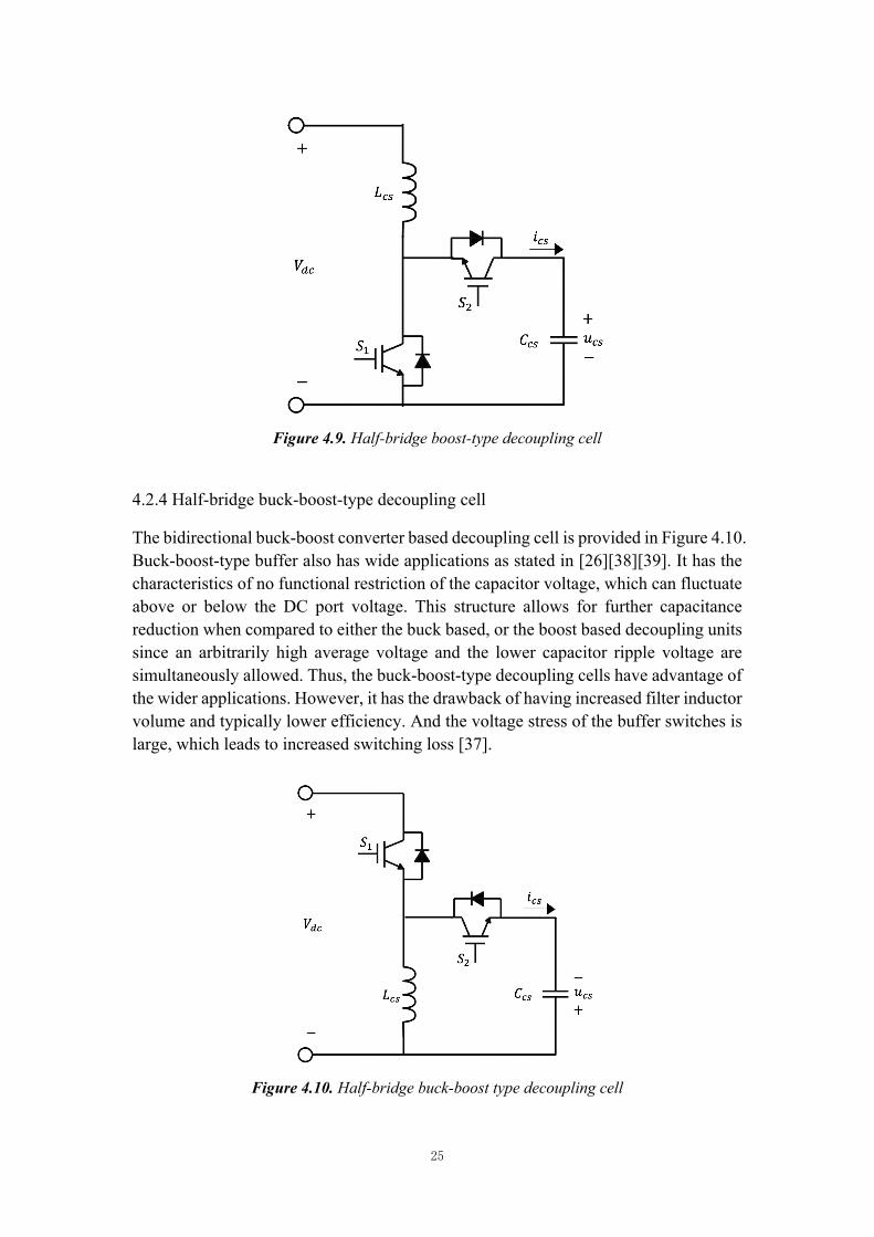
4.2.3 Half-bridge boost-type decoupling cell
Similar to the buck-type decoupling cell, the boost-type decoupling cell illustrated in Figure 4.9 is obtained from the circuit in Figure 4.6. A large number of papers focus on the application of this decoupling schematic [25][34]-[37]. The capacitor voltage is required to be higher than the DC bus voltage in order to operate correctly. This leads to unused energy storage in the ripple capacitor like using a DC bus capacitor. However, the difference of this decoupling cell is that the overall capacitance can be reduced since the high ripple voltage allowed across the capacitor because of the quadratic dependence of the energy with the voltage across the capacitor.
25
Figure 4.9. Half-bridge boost-type decoupling cell
4.2.4 Half-bridge buck-boost-type decoupling cell
The bidirectional buck-boost converter based decoupling cell is provided in Figure 4.10. Buck-boost-type buffer also has wide applications as stated in [26][38][39]. It has the characteristics of no functional restriction of the capacitor voltage, which can fluctuate above or below the DC port voltage. This structure allows for further capacitance reduction when compared to either the buck based, or the boost based decoupling units since an arbitrarily high average voltage and the lower capacitor ripple voltage are simultaneously allowed. Thus, the buck-boost-type decoupling cells have advantage of the wider applications. However, it has the drawback of having increased filter inductor volume and typically lower efficiency. And the voltage stress of the buffer switches is large, which leads to increased switching loss [37].
Figure 4.10. Half-bridge buck-boost type decoupling cell
26
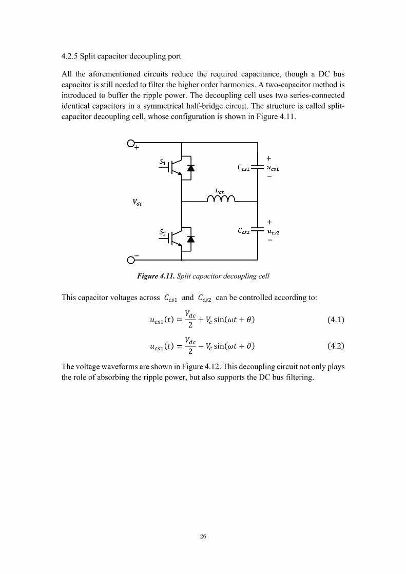
4.2.5 Split capacitor decoupling port
All the aforementioned circuits reduce the required capacitance, though a DC bus capacitor is still needed to filter the higher order harmonics. A two-capacitor method is introduced to buffer the ripple power. The decoupling cell uses two series-connected identical capacitors in a symmetrical half-bridge circuit. The structure is called split-capacitor decoupling cell, whose configuration is shown in Figure 4.11.
Figure 4.11. Split capacitor decoupling cell
This capacitor voltages across 𝐶,.0 and 𝐶,.1 can be controlled according to:
𝑢,.0(𝑡) =𝑉6,2 + 𝑉, sin(𝜔𝑡 + 𝜃) (4.1)
𝑢,.0(𝑡) =𝑉6,2 − 𝑉, sin(𝜔𝑡 + 𝜃) (4.2)
The voltage waveforms are shown in Figure 4.12. This decoupling circuit not only plays the role of absorbing the ripple power, but also supports the DC bus filtering.
27
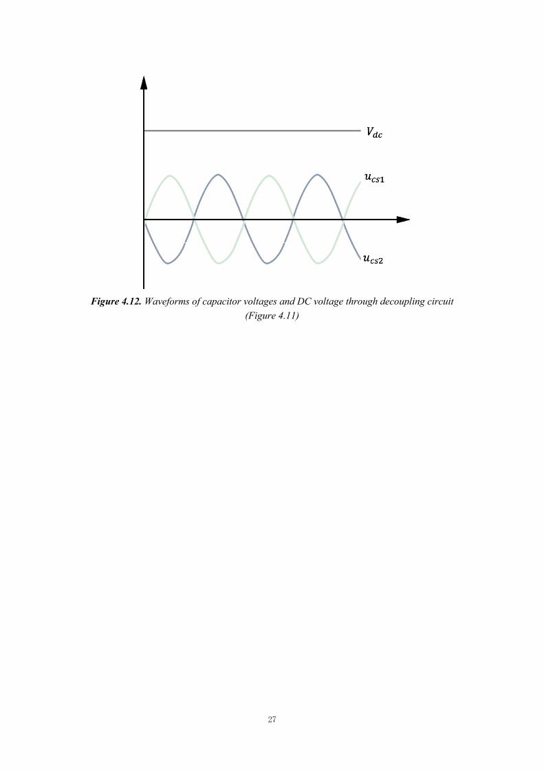
Figure 4.12. Waveforms of capacitor voltages and DC voltage through decoupling circuit
(Figure 4.11)
28
Chapter 5
Active Power Decoupling
Model Design
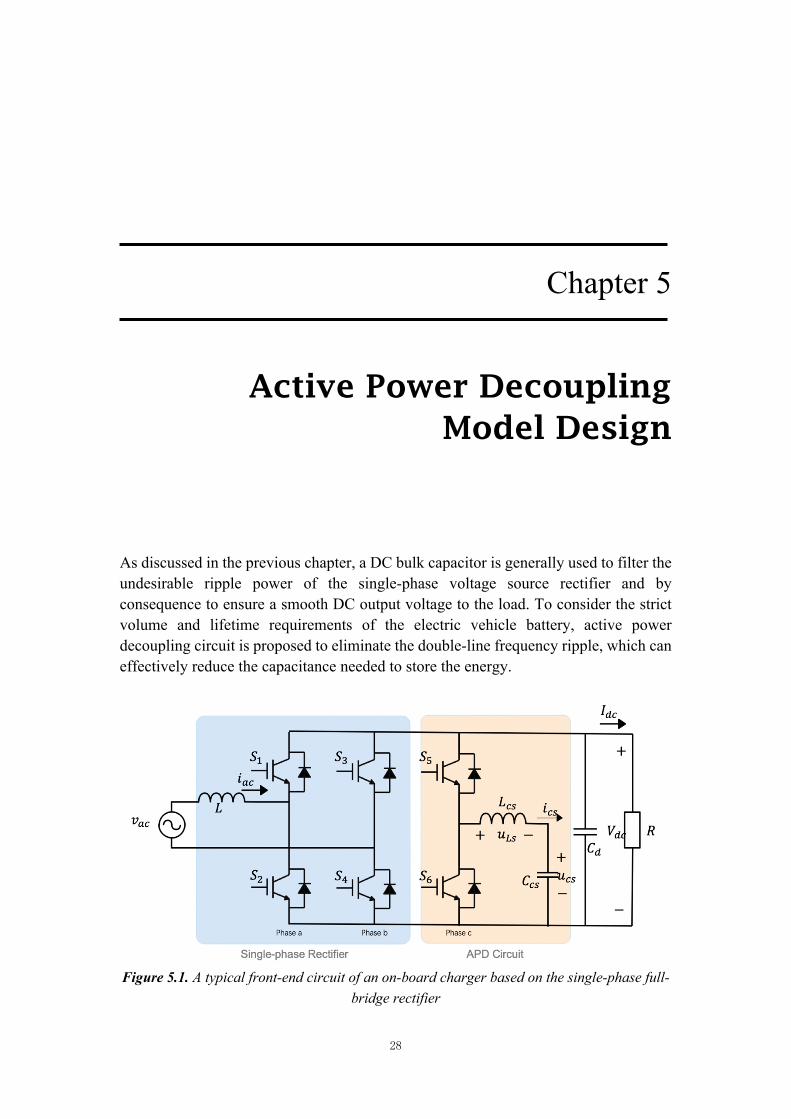
As discussed in the previous chapter, a DC bulk capacitor is generally used to filter the undesirable ripple power of the single-phase voltage source rectifier and by consequence to ensure a smooth DC output voltage to the load. To consider the strict volume and lifetime requirements of the electric vehicle battery, active power decoupling circuit is proposed to eliminate the double-line frequency ripple, which can effectively reduce the capacitance needed to store the energy.
Figure 5.1. A typical front-end circuit of an on-board charger based on the single-phase full-
bridge rectifier
29
This chapter presents the theoretical design of the buck-type based charging system as the circuit shown in Figure 5.1. Firstly, an single-phase AC-DC converter without buffer circuit is analyzed, and the capacitance of the requirements for the passive DC capacitor in the circuit is stated. Secondly, the charging system with added buck-type active power decoupling circuit is investigated. The system power flow is discussed and the ripple power through the buffer is defined. Finally, the mathematical model of the system for simulation is derived according to the defined suitable feedback control strategy.
5.1 Charging System with Passive Decoupling Design
It assumes that the system input is an ideal AC source with a pure sinusoidal voltage 𝑣9, and a pure sinusoidal current 𝑖9,. The phase difference between them is 𝜑. The input frequency is 𝑓 and the corresponding angular frequency is 𝜔.
𝑣9,(𝑡) = 𝑉9, sin(𝜔𝑡) (5.1)
𝑖9,(𝑡) = 𝐼9, sin(𝜔𝑡 − 𝜑) (5.2)
𝜔 = 2𝜋𝑓 (5.3)
where 𝑉9, and 𝐼9, represent the peak value of the input voltage and the input current respectively.
Figure 5.2. Power distribution of the system with passive power decoupling
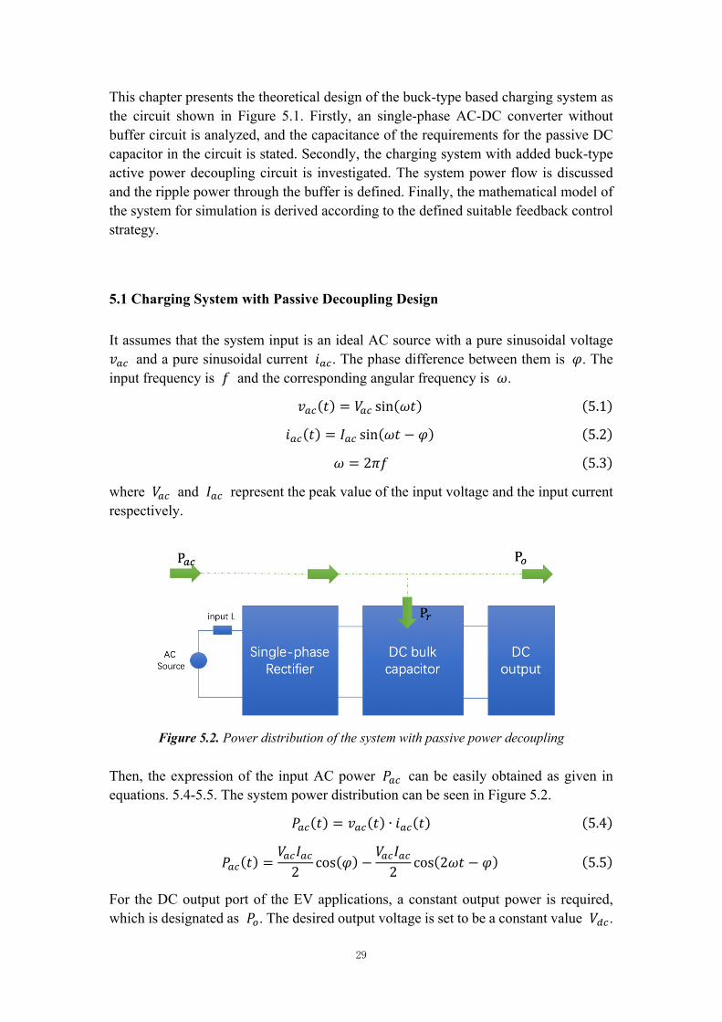
Then, the expression of the input AC power 𝑃9, can be easily obtained as given in equations. 5.4-5.5. The system power distribution can be seen in Figure 5.2.
𝑃9,(𝑡) = 𝑣9,(𝑡) ∙ 𝑖9,(𝑡) (5.4)
𝑃9,(𝑡) =𝑉9,𝐼9,2 cos(𝜑) −
𝑉9,𝐼9,2 cos(2𝜔𝑡 − 𝜑) (5.5)
For the DC output port of the EV applications, a constant output power is required, which is designated as 𝑃i. The desired output voltage is set to be a constant value 𝑉6,.
30
𝑃6, = 𝑃F = 𝑉6, ∙ 𝐼6, (5.6)
From equation 5.5, it can be seen that the input AC power consists of a constant part and a time-varying part. The constant part represents the average power of the input port. And this is the power fed to the DC load. The time-varying part is oscillating at the frequency twice of the line frequency. This second-order harmonic power is defined as the ripple power 𝑃8, which goes to the decoupling capacitor 𝐶()*+. The relationship between the real power and apparent power gives
𝑃i = 𝑆 ∙ cos(𝜑) =𝑉9,𝐼9,2 cos(𝜑) (5.7)
The apparent power is fixed based on the input AC source. If a unity power factor operation is ensured (𝜑 = 0), the maximum output power can be obtained. The power expressions become
𝑃F =𝑉9,𝐼9,2
(5.8)
𝑃8 = −𝑉9,𝐼9,2 cos(2𝜔𝑡) = −𝑃F cos(2𝜔𝑡) (5.9)
When the instantaneous ripple power is positive, the DC capacitor will store the energy. While the ripple power is negative, the DC capacitor will release the energy back to the DC port. The voltage across the DC capacitor is equal to the output voltage. The capacitor current is expressed as:
𝑖,(𝑡) = −𝑃F𝑉6,
cos(2𝜔𝑡) (5.10)
In reality, the output voltage is non-ideal, which comprises of the desired output 𝑉6, and a small-signal vibration 𝑣o. In this paper, the allowed DC output voltage ripple rate is defined as 𝑟. Hence, the peak-to-peak ripple voltage ∆𝑉 is designated as
∆𝑉 = 2𝑟 ∙ 𝑉6, (5.11)
Consider the voltage and current of the DC-link capacitor
𝑣, = 𝑉6, + 𝑣o (5.12)
𝑖,(𝑡) = 𝐶()*+𝑑𝑣,𝑑𝑡
= 𝐶()*+𝑑𝑣o𝑑𝑡
(5.13)
The small-signal vibration voltage is implied as a second-order signal
𝑣o(𝑡) = −∆𝑉2 sin(2𝜔𝑡) (5.14)
Then, it can be calculated that
𝑖,(𝑡) = −𝜔𝐶()*+∆𝑉 cos(2𝜔𝑡) (5.15)
31
Finally, the required capacitance for the passive filter can be obtained by comparing equation 5.10 and 5.15.
𝐶()*+ =𝑃i
2𝜋𝑓𝑉6,∆𝑉(5.16)
5.2 Buck-type Decoupling Cell Design
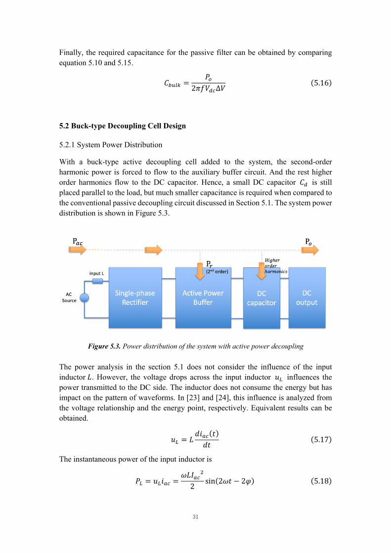
5.2.1 System Power Distribution
With a buck-type active decoupling cell added to the system, the second-order harmonic power is forced to flow to the auxiliary buffer circuit. And the rest higher order harmonics flow to the DC capacitor. Hence, a small DC capacitor 𝐶6 is still placed parallel to the load, but much smaller capacitance is required when compared to the conventional passive decoupling circuit discussed in Section 5.1. The system power distribution is shown in Figure 5.3.
Figure 5.3. Power distribution of the system with active power decoupling
The power analysis in the section 5.1 does not consider the influence of the input inductor𝐿. However, the voltage drops across the input inductor 𝑢- influences the power transmitted to the DC side. The inductor does not consume the energy but has impact on the pattern of waveforms. In [23] and [24], this influence is analyzed from the voltage relationship and the energy point, respectively. Equivalent results can be obtained.
𝑢- = 𝐿𝑑𝑖9,(𝑡)𝑑𝑡
(5.17)
The instantaneous power of the input inductor is
𝑃- = 𝑢-𝑖9, =𝜔𝐿𝐼9,1
2sin(2𝜔𝑡 − 2𝜑) (5.18)
32
Therefore, the re-defined second-order ripple power 𝑃8 can be obtained by subtracting equation 5.18 from equation 5.9.
𝑃8 = −[𝑉9,𝐼9,2
cos(2𝜔𝑡 − 𝜑) +𝜔𝐿𝐼9,1
2sin(2𝜔𝑡 − 2𝜑)] (5.19)
This equation can be further expressed in the sinusoidal form
𝑃8 = s𝑉9,1𝐼9,1
4 cos1 𝜑 + t𝜔𝐿𝐼9,1
2 −𝑉9,𝐼9,2 sin𝜑u
1
∙ sin(2𝜔𝑡 − 2𝜑 + 𝜓) (5.20)
𝜓 = tany0(𝑉9,𝐼9, 2⁄ ) cos𝜑
{𝜔𝐿𝐼9,1 2⁄ | − (𝑉9,𝐼9, 2⁄ ) sin𝜑 (5.21)
Here it defines the amplitude of the ripple power waveform as 𝑃8_39:, by substituting equation 5.7
𝑃8_39: = s𝑃i1 + t2𝜔𝐿𝑃i1
𝑉9,1 cos1 𝜑− 𝑃i
sin𝜑cos𝜑u
1
(5.22)
It can be concluded that the overall ripple power consists of two parts: One is the unbalanced power between the input and output, which is the characteristic of the AC-DC converter; Another part is resulted from the input inductor, which is only noticeable if the inductance or the line frequency is high. Also, this maximum value of the ripple power is related to the system power factor. Similar to the equation 5.16, the required DC capacitor value when considering the influence of the input inductor can be re-defined as
𝐶()*+ =𝑃8_39:
2𝜋𝑓𝑉6,∆𝑉(5.23)
The APD LC filter in Figure 5.4 is designed to compensate the second-order ripple, it implies that the current flowed through the circuit 𝑖,. is sinusoidal wave with double line frequency and an amplitude of 𝐼,..
33
Figure 5.4. Buck-type active power decoupling circuit
𝑖,. = 𝐼,. sin(2𝜔𝑡 + 𝛽) (5.24)
The voltage across the capacitor 𝑢,. can be obtained by the integration of the current. It assumes that the average capacitor voltage is 𝑉~ , then the capacitor voltage is
𝑢,. = 𝑉~ +1𝐶,.
� 𝑖,.𝑑𝑡 = 𝑉~ −1
2𝜔𝐶,.𝐼,. sin(2𝜔𝑡 + 𝛽) (5.25)
Then, the power through the APD circuit can be calculated as
𝑃,. = 𝑖,. ∙ (𝑢-. + 𝑢,.) (5.26)
𝑢-. = 𝐿,.𝑑𝑖,.𝑑𝑡
(5.27)
𝑃,. = 𝑉~𝐼,. sin(2𝜔𝑡 + 𝛽) + �𝜔𝐿,. −0
������ 𝐼,.1 sin(4𝜔𝑡 + 2𝛽) (5.28)
It can be realized that this power is composed of two components: A second-order component that matches the ripple power defined in equation 5.20; A fourth-order component generated in the APD circuit that is then absorbed by the DC capacitor.
5.2.2 Active Power Decoupling Capacitor Design
The capacitance value of the buffer capacitor has a significant impact on the capacitor volume. The voltage and current through the buck-type active decoupling circuit are analyzed in order to determine the value of the buffer capacitor 𝐶,. and inductor 𝐿,.. The active power decoupling capacitor acts as the energy storage element, while the inductor is used to be the energy transfer component for transferring the ripple energy between the APD capacitor and the DC output. The switches S5 and S6 are controlled to realize this power transformation. The instantaneous power is selected as the reference control signal. When the instantaneous AC power is higher than the DC power, the switch S5 works to transfer the ripple energy to the APD circuit. The APD inductor and capacitor are charged during the turn-on interval of S5, while the inductor
34
then releases the energy to the capacitor as S5 turned off. On the contrary, when the instantaneous AC power is lower than the DC power, the switch S6 functions to transfer the stored energy from the APD circuit back to the DC output. The turn-on interval of S6 allows the capacitor charging the inductor, while both the inductor and capacitor release the ripple energy to the DC side during the turn-off period. If it is assumed that all the second-order ripple power is only stored in the APD capacitor. Neglects other effects, the expression of the capacitor voltage and current can be determined as follows
𝑃8 = 𝑢,. ∙ 𝑖,. (5.29)
𝑢,. ∙ 𝐶,.𝑑𝑢,.𝑑𝑡
= 𝑃8_39: sin(2𝜔𝑡 − 2𝜑 + 𝜓) (5.30)
By solving the above deviation equation
�𝑢,. ∙ 𝑢,.�𝑑𝑡 = �𝑃8_39:𝐶,.
sin(2𝜔𝑡 − 2𝜑 + 𝜓)𝑑𝑡 (5.31)
�𝑢,. ∙ 𝑢,.� 𝑑𝑡 = 𝑢,. �𝑢,.� 𝑑𝑡 − �𝑢,.� ∙ ��𝑢,.� 𝑑𝑡� 𝑑𝑡 (5.32)
= 𝑢,.1 − �𝑢,. ∙ 𝑢,.� 𝑑𝑡
𝑢,.1 = 2�𝑃8_39:𝐶,.
sin(2𝜔𝑡 − 2𝜑 + 𝜓)𝑑𝑡 (5.33)
Finally, it gives that
𝑢,. = s𝑃8_39:𝐶,.𝜔
[− cos(2𝜔𝑡 − 2𝜑 + 𝜓) + 𝐾] (5.34)
𝑖,. = 𝑃8_39: sin(2𝜔𝑡 − 2𝜑 + 𝜓)
𝑢,.(5.35)
Here K is a constant value that is determined by the maximum capacitor voltage, capacitor value and the maximum ripple power. It represents the maximum energy storage of the APD capacitor compared to the ripple energy.
𝐾 =𝑢,._39:1𝐶,.𝜔
𝑃8_39:− 1 (5.36)
𝐸8𝐸,._39:
=2
𝐾 + 1(5.37)
When 𝐾 = 1, it means that the APD capacitor is fully charged and discharged by the ripple energy. This is the energy storage margin that the capacitor should fulfil when selecting a capacitor value. The maximum energy storage allowed should be always larger than the ripple energy to provide a redundancy, which ensures the system safety.
35
However, these derivations require the APD circuit to work in the boundary conduction mode (BCM) or the discontinuous conduction mode (DCM). So that the capacitor stores all the energy and the inductor is only used for energy transfer. And therefore, a minimum capacitance value for the APD capacitor can be determined in case of 𝐾 =1 and the capacitor charged and discharged between zero and the DC bus voltage.
𝐶,._345 =2𝑃8_39:𝜔𝑉6,1
(5.38)
The above derivations of the capacitor current and voltage are based on the assumption that the ripple power through the capacitor is pure sinusoidal. The output voltage is considered to be non-ideal with the ripple component. However, if the active power decoupling circuit is working in the continuous conduction mode (CCM), it cannot guarantee that all the ripple energy is transferred to the capacitor. To obtain the expression of the capacitor current and voltage, it assumes that the output voltage ripple is neglectable and the capacitor current through the APD circuit (𝑖,.) is pure sinusoidal. The current can be expressed by dividing the ripple power in equation 5.20 by the DC voltage 𝑉6,. The voltage can be acquired by the integral of the current.
𝑖,. =𝑃8_39:𝑉6,
sin(2𝜔𝑡 − 2𝜑 + 𝜓) (5.39)
𝑢,. = −𝑃8_39:
𝑉6, ∙ 2𝜔𝐶,.cos(2𝜔𝑡 − 2𝜑 + 𝜓) +𝑀 (5.40)
Here M is a constant that represents the defined average capacitor value.
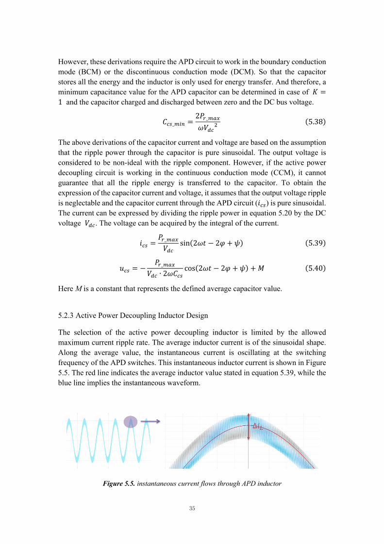
5.2.3 Active Power Decoupling Inductor Design
The selection of the active power decoupling inductor is limited by the allowed maximum current ripple rate. The average inductor current is of the sinusoidal shape. Along the average value, the instantaneous current is oscillating at the switching frequency of the APD switches. This instantaneous inductor current is shown in Figure 5.5. The red line indicates the average inductor value stated in equation 5.39, while the blue line implies the instantaneous waveform.
Figure 5.5. instantaneous current flows through APD inductor
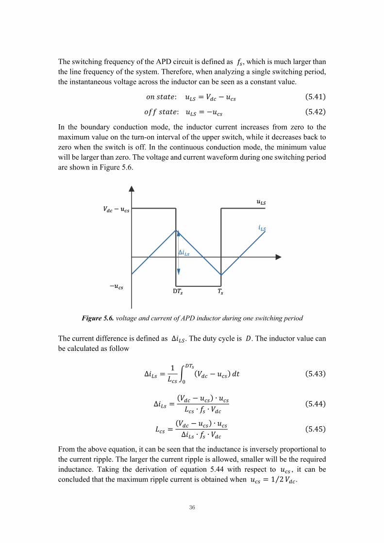
36
The switching frequency of the APD circuit is defined as 𝑓., which is much larger than the line frequency of the system. Therefore, when analyzing a single switching period, the instantaneous voltage across the inductor can be seen as a constant value.
𝑜𝑛𝑠𝑡𝑎𝑡𝑒:𝑢-� = 𝑉6, − 𝑢,. (5.41)
𝑜𝑓𝑓𝑠𝑡𝑎𝑡𝑒:𝑢-� = −𝑢,. (5.42)
In the boundary conduction mode, the inductor current increases from zero to the maximum value on the turn-on interval of the upper switch, while it decreases back to zero when the switch is off. In the continuous conduction mode, the minimum value will be larger than zero. The voltage and current waveform during one switching period are shown in Figure 5.6.
Figure 5.6. voltage and current of APD inductor during one switching period
The current difference is defined as ∆𝑖-�. The duty cycle is 𝐷. The inductor value can be calculated as follow
∆𝑖-. =1𝐿,.
� (𝑉6, − 𝑢,.)���
F𝑑𝑡 (5.43)
∆𝑖-. =(𝑉6, − 𝑢,.) ∙ 𝑢,.𝐿,. ∙ 𝑓. ∙ 𝑉6,
(5.44)
𝐿,. =(𝑉6, − 𝑢,.) ∙ 𝑢,.∆𝑖-. ∙ 𝑓. ∙ 𝑉6,
(5.45)
From the above equation, it can be seen that the inductance is inversely proportional to the current ripple. The larger the current ripple is allowed, smaller will be the required inductance. Taking the derivation of equation 5.44 with respect to 𝑢,. , it can be concluded that the maximum ripple current is obtained when 𝑢,. = 1 2⁄ 𝑉6,.
37
5.3 Results and Analysis of the Mathematical Model
The mathematical model of the charging system is discussed in the above sections, which includes the system power flow, the current and voltage through the buck-type active power decoupling cell. In this section, the theoretical model is built in MATLAB with a given system specification. Firstly, the impacts of different parameters on the selection of the APD capacitor are investigated. Then, the current waveform and voltage waveform through the APD capacitor are generated with a set of chosen value. The waveforms will be compared with the simulated results in the next chapter. For the electric vehicle application, the input source of the charger is generally connected to the grid, which normally has a frequency of 50 Hz and the amplitude of 325 V. The output port is connected to the battery to provide a constant DC voltage. The DC voltage of approximately 400 V is commonly chosen. The overall system specification is identified in Table 5.1.
Table 5.1. Charging system specification SYMBOL VALUE
Apparent Power 𝑆 3.3 kVA
Grid Frequency 𝑓 50 Hz
Grid Peak Voltage 𝑉9, 325 V Output Voltage 𝑉6, 400 V
Output Voltage Ripple 𝑟 ±2%
Input Inductor 𝐿 1 mH Switching Frequency 𝑓. 36 kHz
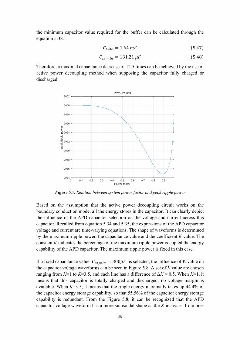
From the above values, it can be calculated that the acceptable peak-to-peak voltage ripple at the output port is 16 V. According to equation 5.22, the peak value of the ripple power varies slightly as function of the system power factor. In Figure 5.7, this relationship is shown. When a unit power factor is chosen, the maximum value of the ripple power amplitude is obtained. In the theoretical calculation and the simulation in the next chapter, a power factor 𝑝𝑓 = 0.999 is applied. Under these conditions, the amplitude of ripple power waveform can be calculated according to equation 5.22.
𝑃8_39: = 3.2977𝑘𝑊 (5.46)
Then, the required capacitance for the passive power decoupling method is estimated via equation 5.23. Afterwards, when using a buck-type active power decoupling method,
38
the minimum capacitor value required for the buffer can be calculated through the equation 5.38.
𝐶()*+ = 1.64𝑚𝐹 (5.47)
𝐶,._345 = 131.21𝜇𝐹 (5.48)
Therefore, a maximal capacitance decrease of 12.5 times can be achieved by the use of active power decoupling method when supposing the capacitor fully charged or discharged.
Figure 5.7. Relation between system power factor and peak ripple power
Based on the assumption that the active power decoupling circuit works on the boundary conduction mode, all the energy stores in the capacitor. It can clearly depict the influence of the APD capacitor selection on the voltage and current across this capacitor. Recalled from equation 5.34 and 5.35, the expressions of the APD capacitor voltage and current are time-varying equations. The shape of waveforms is determined by the maximum ripple power, the capacitance value and the coefficient K value. The constant K indicates the percentage of the maximum ripple power occupied the energy capability of the APD capacitor. The maximum ripple power is fixed in this case. If a fixed capacitance value 𝐶,._345 = 300𝜇𝐹 is selected, the influence of K value on the capacitor voltage waveforms can be seen in Figure 5.8. A set of K value are chosen ranging from K=1 to K=3.5, and each line has a difference of ΔK = 0.5. When K=1, it means that this capacitor is totally charged and discharged, no voltage margin is available. When K=3.5, it means that the ripple energy maximally takes up 44.4% of the capacitor energy storage capability, so that 55.56% of the capacitor energy storage capability is redundant. From the Figure 5.8, it can be recognized that the APD capacitor voltage waveform has a more sinusoidal shape as the K increases from one.
0 0.1 0.2 0.3 0.4 0.5 0.6 0.7 0.8 0.9 1Power factor
2984
2986
2988
2990
2992
2994
2996
2998
3000
3002
peak
ripp
le p
ower
Pf vs. Prpeak
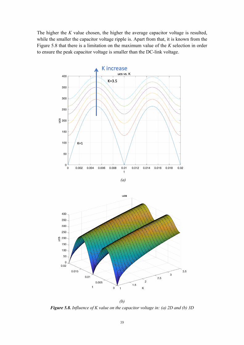
39
The higher the K value chosen, the higher the average capacitor voltage is resulted, while the smaller the capacitor voltage ripple is. Apart from that, it is known from the Figure 5.8 that there is a limitation on the maximum value of the K selection in order to ensure the peak capacitor voltage is smaller than the DC-link voltage.
(a)
(b)
Figure 5.8. Influence of K value on the capacitor voltage in: (a) 2D and (b) 3D
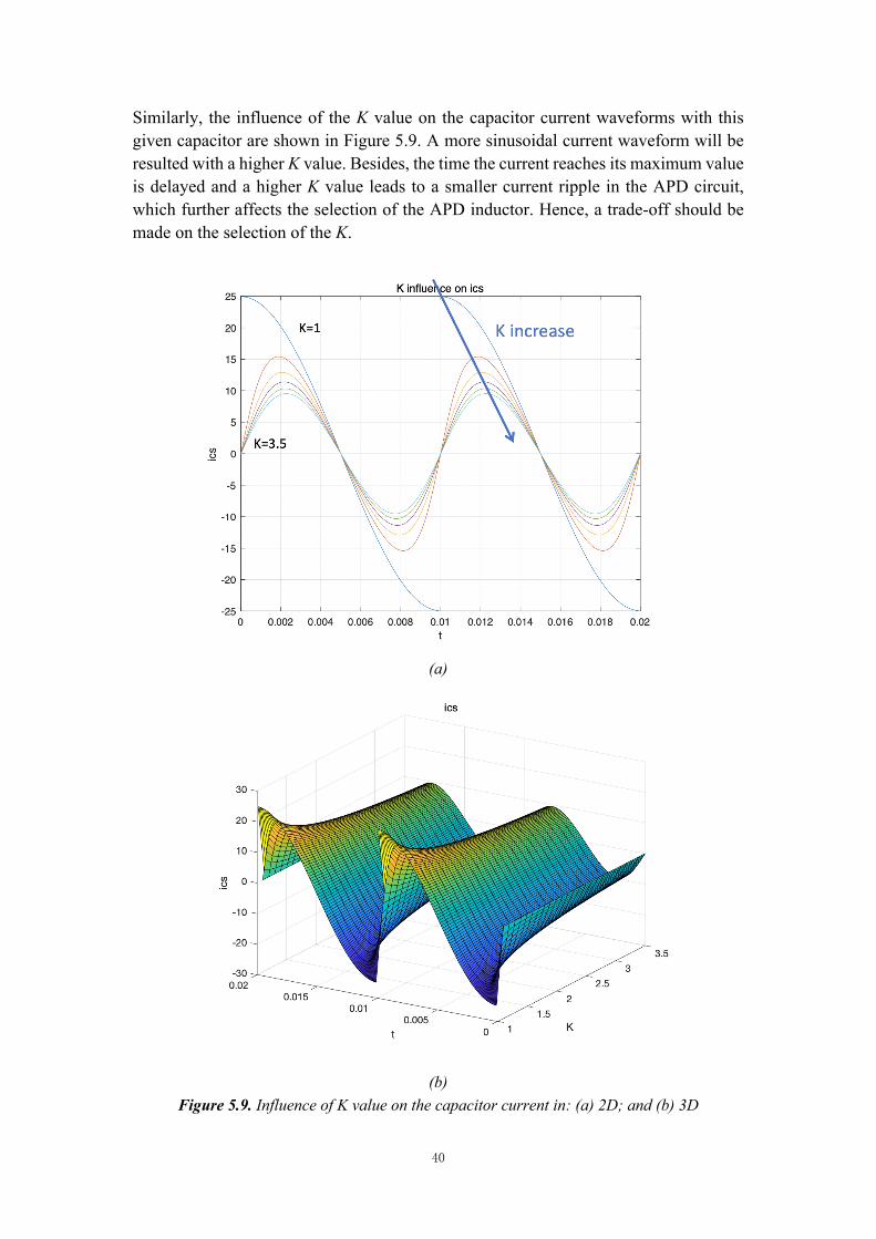
40
Similarly, the influence of the K value on the capacitor current waveforms with this given capacitor are shown in Figure 5.9. A more sinusoidal current waveform will be resulted with a higher K value. Besides, the time the current reaches its maximum value is delayed and a higher K value leads to a smaller current ripple in the APD circuit, which further affects the selection of the APD inductor. Hence, a trade-off should be made on the selection of the K.
(a)
(b)
Figure 5.9. Influence of K value on the capacitor current in: (a) 2D; and (b) 3D
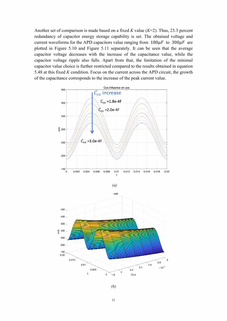
41
Another set of comparison is made based on a fixed K value (K=2). Thus, 23.3 percent redundancy of capacitor energy storage capability is set. The obtained voltage and current waveforms for the APD capacitors value ranging from 180𝜇𝐹 to 300𝜇𝐹 are plotted in Figure 5.10 and Figure 5.11 separately. It can be seen that the average capacitor voltage decreases with the increase of the capacitance value, while the capacitor voltage ripple also falls. Apart from that, the limitation of the minimal capacitor value choice is further restricted compared to the results obtained in equation 5.48 at this fixed K condition. Focus on the current across the APD circuit, the growth of the capacitance corresponds to the increase of the peak current value.
(a)
(b)
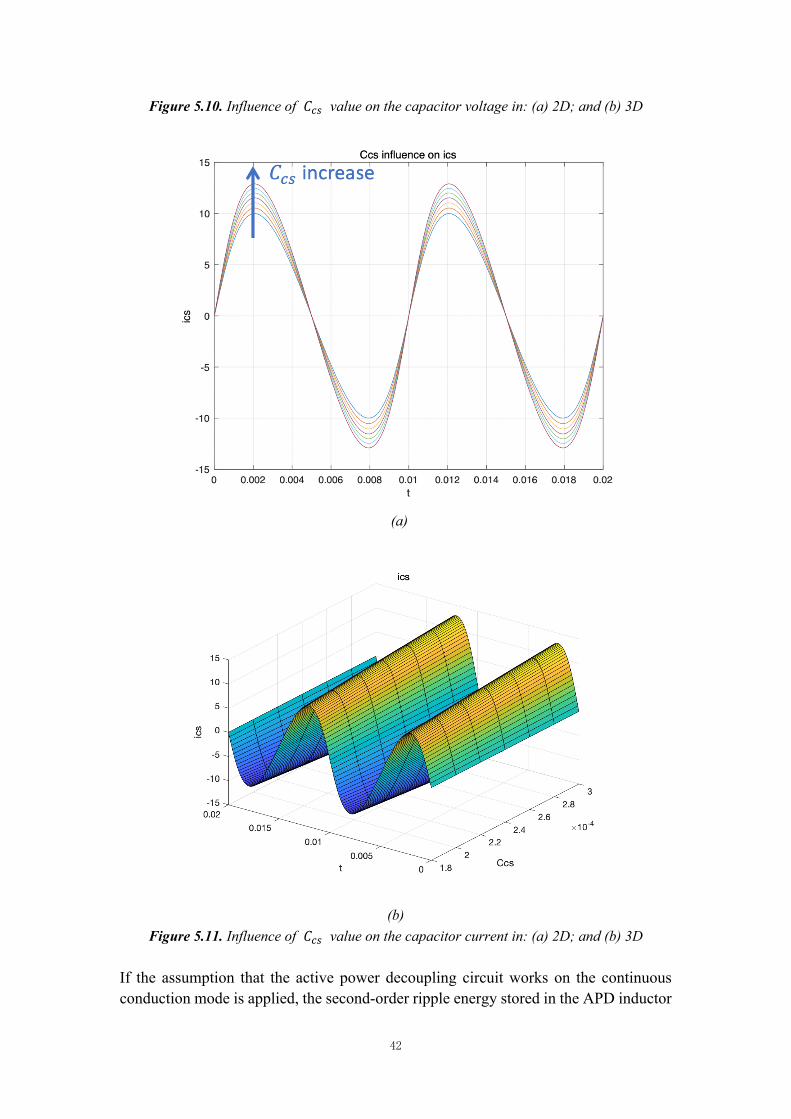
42
Figure 5.10. Influence of 𝐶,. value on the capacitor voltage in: (a) 2D; and (b) 3D
(a)
(b)
Figure 5.11. Influence of 𝐶,. value on the capacitor current in: (a) 2D; and (b) 3D
If the assumption that the active power decoupling circuit works on the continuous conduction mode is applied, the second-order ripple energy stored in the APD inductor
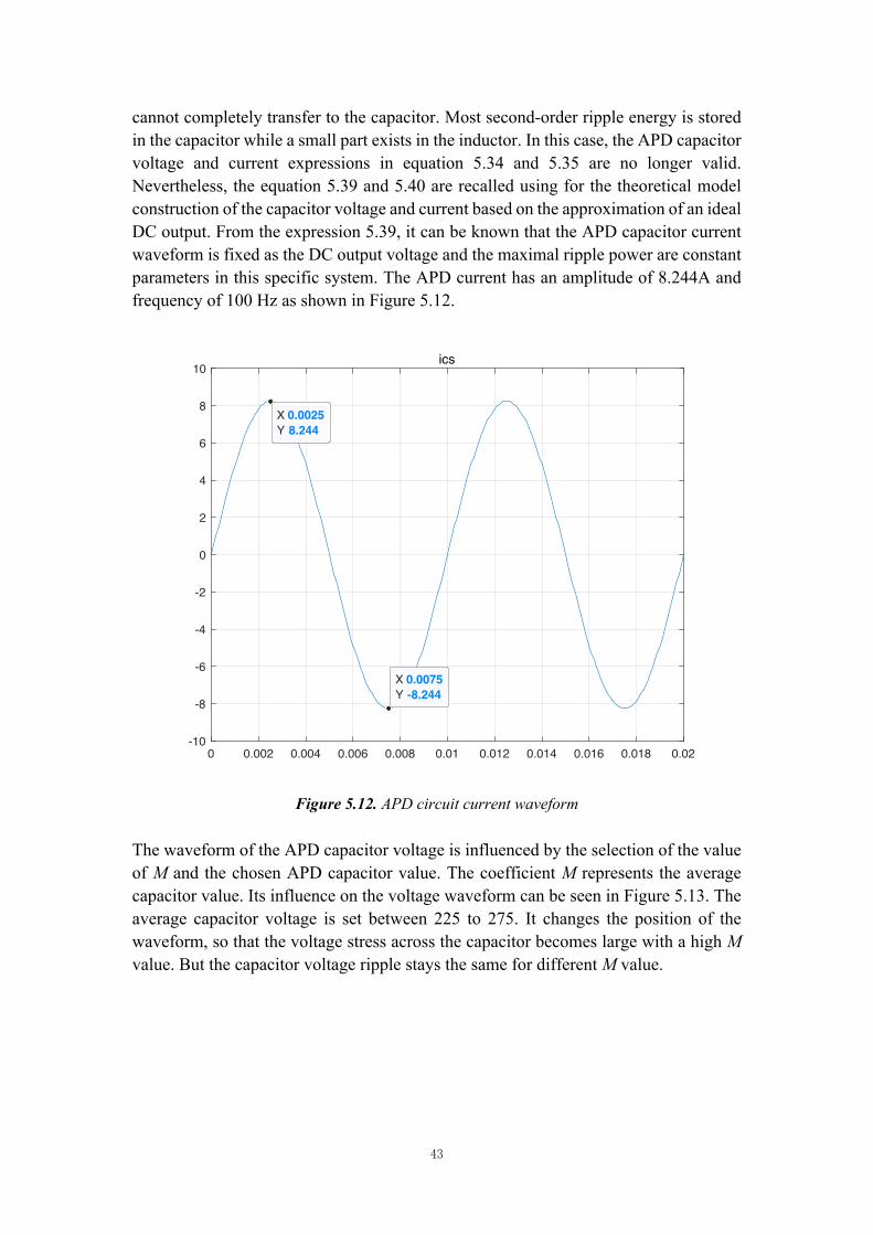
43
cannot completely transfer to the capacitor. Most second-order ripple energy is stored in the capacitor while a small part exists in the inductor. In this case, the APD capacitor voltage and current expressions in equation 5.34 and 5.35 are no longer valid. Nevertheless, the equation 5.39 and 5.40 are recalled using for the theoretical model construction of the capacitor voltage and current based on the approximation of an ideal DC output. From the expression 5.39, it can be known that the APD capacitor current waveform is fixed as the DC output voltage and the maximal ripple power are constant parameters in this specific system. The APD current has an amplitude of 8.244A and frequency of 100 Hz as shown in Figure 5.12.
Figure 5.12. APD circuit current waveform
The waveform of the APD capacitor voltage is influenced by the selection of the value of M and the chosen APD capacitor value. The coefficient M represents the average capacitor value. Its influence on the voltage waveform can be seen in Figure 5.13. The average capacitor voltage is set between 225 to 275. It changes the position of the waveform, so that the voltage stress across the capacitor becomes large with a high M value. But the capacitor voltage ripple stays the same for different M value.
0 0.002 0.004 0.006 0.008 0.01 0.012 0.014 0.016 0.018 0.02-10
-8
-6
-4
-2
0
2
4
6
8
10ics
X 0.0025Y 8.244
X 0.0075Y -8.244
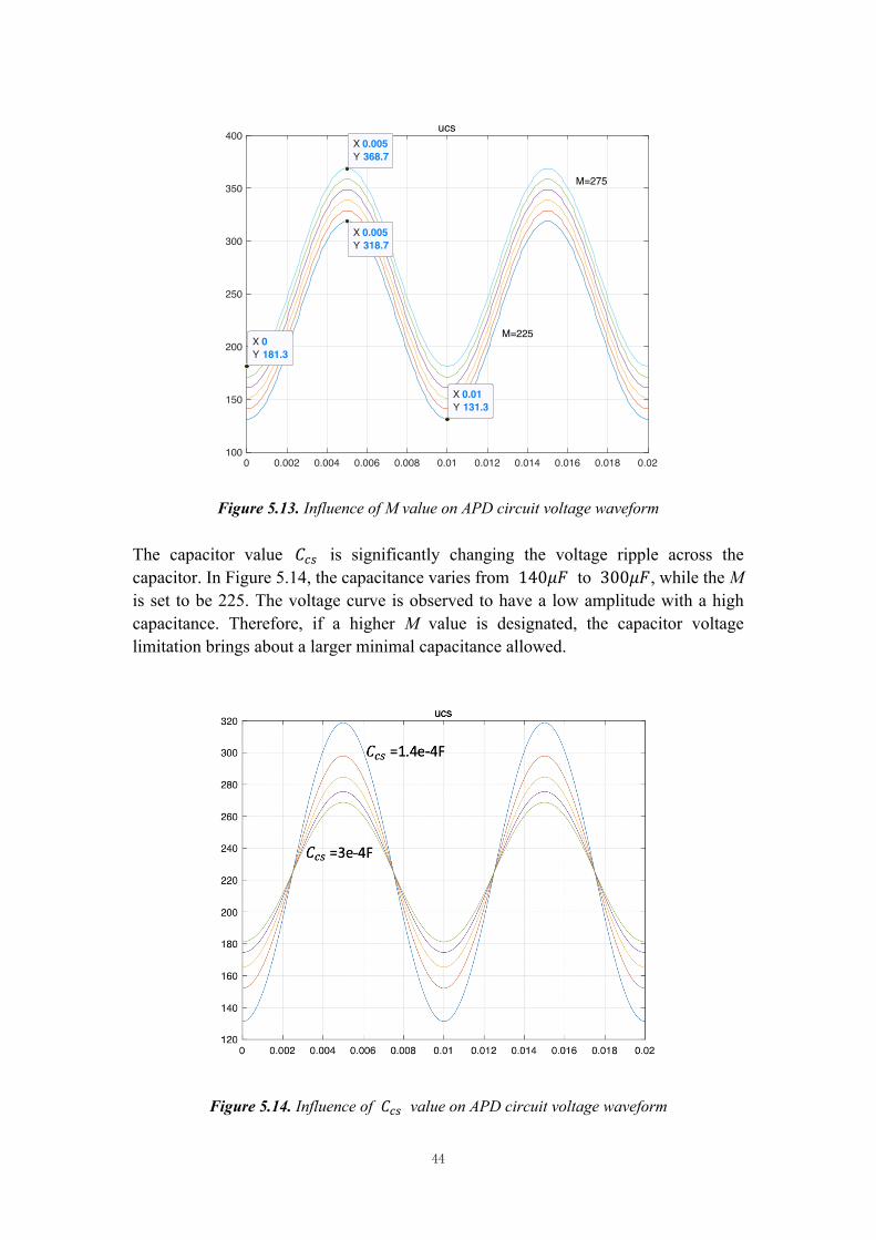
44
Figure 5.13. Influence of M value on APD circuit voltage waveform
The capacitor value 𝐶,. is significantly changing the voltage ripple across the capacitor. In Figure 5.14, the capacitance varies from 140𝜇𝐹 to 300𝜇𝐹, while the M is set to be 225. The voltage curve is observed to have a low amplitude with a high capacitance. Therefore, if a higher M value is designated, the capacitor voltage limitation brings about a larger minimal capacitance allowed.
Figure 5.14. Influence of 𝐶,. value on APD circuit voltage waveform
0 0.002 0.004 0.006 0.008 0.01 0.012 0.014 0.016 0.018 0.02100
150
200
250
300
350
400ucs
X 0.005Y 368.7
X 0.005Y 318.7
X 0Y 181.3
X 0.01Y 131.3
M=275
M=225

45
The selection of the inductor is only decided by the current through the APD circuit. In the CCM condition, the maximum current value is a fixed value. The only influenced factor for the inductance is the allowed current ripple. With the parameters defined above, the maximum current happens when the 𝑢,. = 200𝑉. If the allowed ripple is set to be 40%, the inductance will be calculated to be 842𝜇𝐻. In the DCM mode, the current is influenced by both the K value and the capacitor value. Therefore, a larger capacitance and a smaller K value requires a smaller inductance. A trade-off should be made between the capacitor and inductor to realize a comparable small volume in this case.
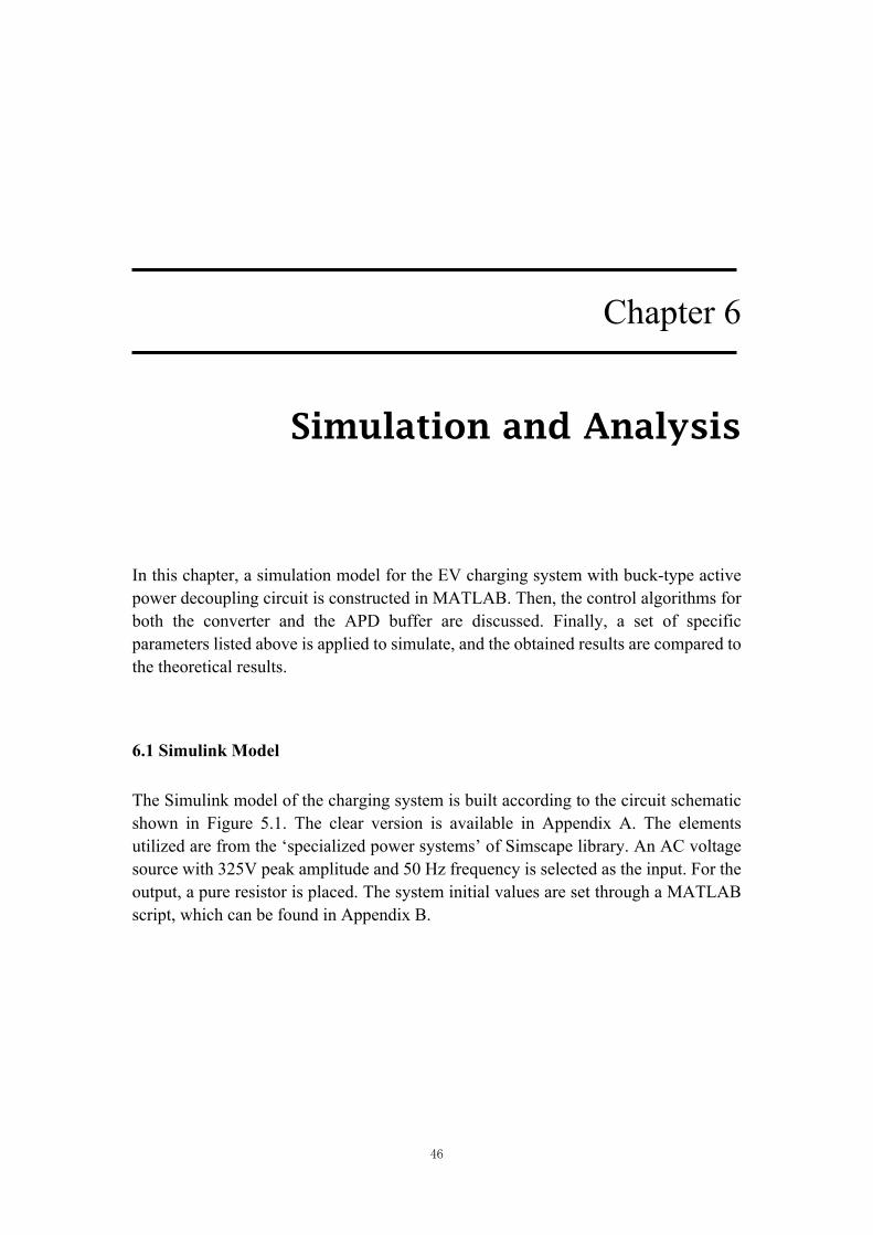
46
Chapter 6
Simulation and Analysis
In this chapter, a simulation model for the EV charging system with buck-type active power decoupling circuit is constructed in MATLAB. Then, the control algorithms for both the converter and the APD buffer are discussed. Finally, a set of specific parameters listed above is applied to simulate, and the obtained results are compared to the theoretical results.
6.1 Simulink Model
The Simulink model of the charging system is built according to the circuit schematic shown in Figure 5.1. The clear version is available in Appendix A. The elements utilized are from the ‘specialized power systems’ of Simscape library. An AC voltage source with 325V peak amplitude and 50 Hz frequency is selected as the input. For the output, a pure resistor is placed. The system initial values are set through a MATLAB script, which can be found in Appendix B.
47
Figure 6.1. Simulink main circuit schematic model
Six IGBT with diode blocks are chosen as the switches in this circuit, which form three bridge-leg phases: a, b and c. The phase a and phase b are connected to the voltage source (or grid side) and work to be the conventional single-phase full-bridge PWM rectifier. And the phase c operates to circulate the second-order pulsating power between the energy storage element and the DC bus. Two control systems are therefore designated to perform these functions. The operation principles are given below.
6.1.1 Rectifier PWM Control Algorithm
The rectifier controller aims to control the average DC-link voltage at the desired level under the circumstance that the system works with unity power factor. The PWM modulation method is designed to accomplish the bi-directional power flow. Two control loops are included. The outer control loop regulates the DC bus voltage with regard to the reference voltage of 400 V, where a proportional-integral (PI) compensator is applied to generate a signal G which is multiplied by the AC voltage to create the AC current reference signal for the inner control loop. The inner control loop regulates the AC-side current referred to the obtained current reference. The resulted current error signal is handled by a second PI compensator afterwards. For improving dynamic performance, especially during grid disturbance, a feedforward open loop is also added to form the final reference voltage for the PWM control. This is derived from the comparison between the measured AC voltage and the reference output voltage.
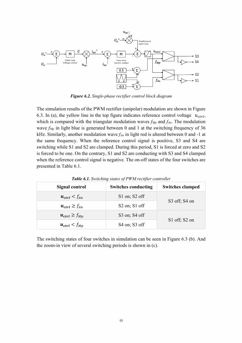
48
Figure 6.2. Single-phase rectifier control block diagram
The simulation results of the PWM rectifier (unipolar) modulation are shown in Figure 6.3. In (a), the yellow line in the top figure indicates reference control voltage 𝑢,J8*, which is compared with the triangular modulation waves fMp and fAn. The modulation wave fMp in light blue is generated between 0 and 1 at the switching frequency of 36 kHz. Similarly, another modulation wave fAn in light red is altered between 0 and -1 at the same frequency. When the reference control signal is positive, S3 and S4 are switching while S1 and S2 are clamped. During this period, S1 is forced at zero and S2 is forced to be one. On the contrary, S1 and S2 are conducting with S3 and S4 clamped when the reference control signal is negative. The on-off states of the four switches are presented in Table 6.1.
Table 6.1. Switching states of PWM rectifier controller
Signal control Switches conducting Switches clamped
𝒖𝒄𝒕𝒓𝒍 < 𝑓<5 S1 on; S2 off S3 off; S4 on
𝒖𝒄𝒕𝒓𝒍 ≥ 𝑓<5 S2 on; S1 off
𝒖𝒄𝒕𝒓𝒍 ≥ 𝑓>? S3 on; S4 off S1 off; S2 on
𝒖𝒄𝒕𝒓𝒍 < 𝑓>? S4 on; S3 off The switching states of four switches in simulation can be seen in Figure 6.3 (b). And the zoom-in view of several switching periods is shown in (c).
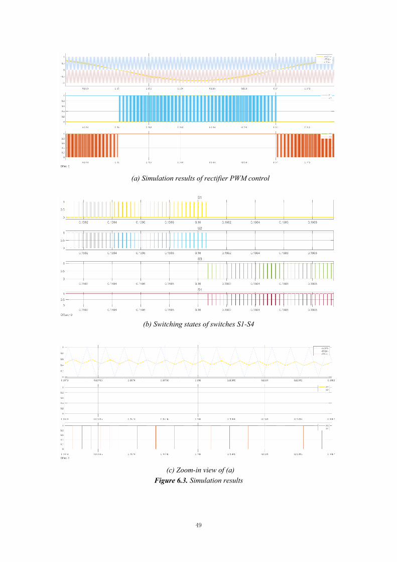
49
(a) Simulation results of rectifier PWM control
(b) Switching states of switches S1-S4
(c) Zoom-in view of (a)
Figure 6.3. Simulation results
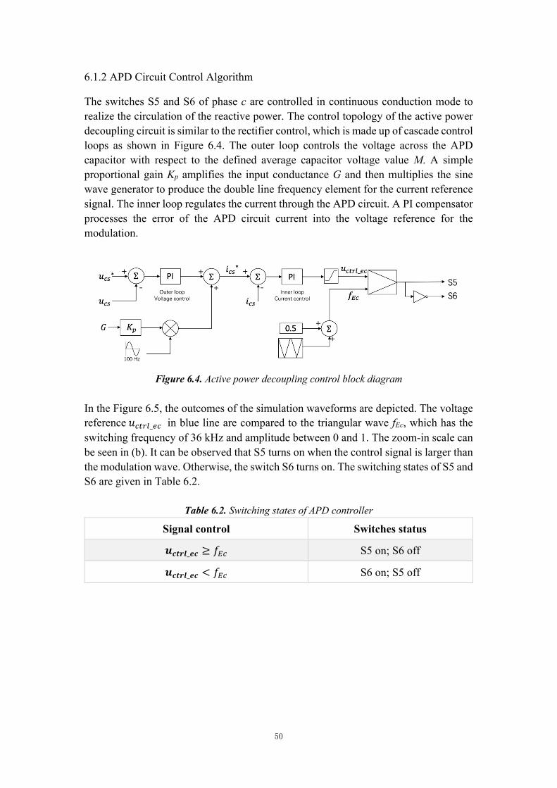
50
6.1.2 APD Circuit Control Algorithm
The switches S5 and S6 of phase c are controlled in continuous conduction mode to realize the circulation of the reactive power. The control topology of the active power decoupling circuit is similar to the rectifier control, which is made up of cascade control loops as shown in Figure 6.4. The outer loop controls the voltage across the APD capacitor with respect to the defined average capacitor voltage value M. A simple proportional gain Kp amplifies the input conductance G and then multiplies the sine wave generator to produce the double line frequency element for the current reference signal. The inner loop regulates the current through the APD circuit. A PI compensator processes the error of the APD circuit current into the voltage reference for the modulation.
Figure 6.4. Active power decoupling control block diagram
In the Figure 6.5, the outcomes of the simulation waveforms are depicted. The voltage reference𝑢,J8*_K, in blue line are compared to the triangular wave fEc, which has the switching frequency of 36 kHz and amplitude between 0 and 1. The zoom-in scale can be seen in (b). It can be observed that S5 turns on when the control signal is larger than the modulation wave. Otherwise, the switch S6 turns on. The switching states of S5 and S6 are given in Table 6.2.
Table 6.2. Switching states of APD controller
Signal control Switches status
𝒖𝒄𝒕𝒓𝒍_𝒆𝒄 ≥ 𝑓=, S5 on; S6 off
𝒖𝒄𝒕𝒓𝒍_𝒆𝒄 < 𝑓=, S6 on; S5 off
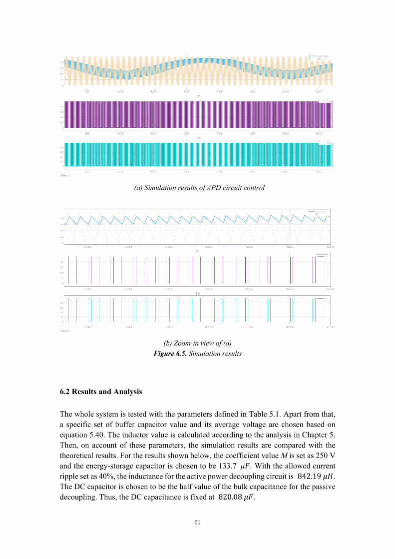
51
(a) Simulation results of APD circuit control
(b) Zoom-in view of (a) Figure 6.5. Simulation results
6.2 Results and Analysis The whole system is tested with the parameters defined in Table 5.1. Apart from that, a specific set of buffer capacitor value and its average voltage are chosen based on equation 5.40. The inductor value is calculated according to the analysis in Chapter 5. Then, on account of these parameters, the simulation results are compared with the theoretical results. For the results shown below, the coefficient value M is set as 250 V and the energy-storage capacitor is chosen to be 133.7 𝜇𝐹. With the allowed current ripple set as 40%, the inductance for the active power decoupling circuit is 842.19𝜇𝐻. The DC capacitor is chosen to be the half value of the bulk capacitance for the passive decoupling. Thus, the DC capacitance is fixed at 820.08𝜇𝐹.
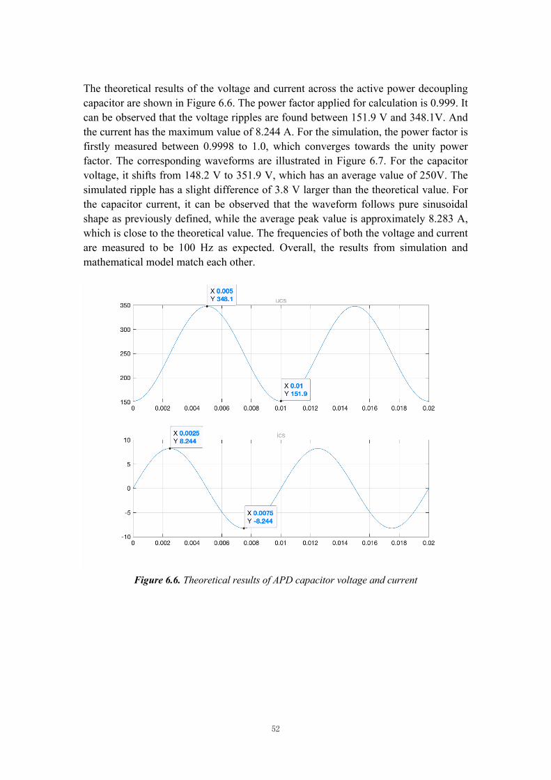
52
The theoretical results of the voltage and current across the active power decoupling capacitor are shown in Figure 6.6. The power factor applied for calculation is 0.999. It can be observed that the voltage ripples are found between 151.9 V and 348.1V. And the current has the maximum value of 8.244 A. For the simulation, the power factor is firstly measured between 0.9998 to 1.0, which converges towards the unity power factor. The corresponding waveforms are illustrated in Figure 6.7. For the capacitor voltage, it shifts from 148.2 V to 351.9 V, which has an average value of 250V. The simulated ripple has a slight difference of 3.8 V larger than the theoretical value. For the capacitor current, it can be observed that the waveform follows pure sinusoidal shape as previously defined, while the average peak value is approximately 8.283 A, which is close to the theoretical value. The frequencies of both the voltage and current are measured to be 100 Hz as expected. Overall, the results from simulation and mathematical model match each other.
Figure 6.6. Theoretical results of APD capacitor voltage and current
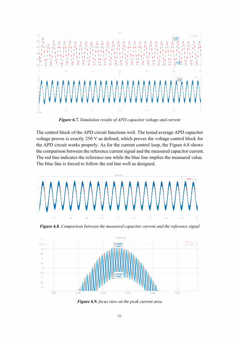
53
Figure 6.7. Simulation results of APD capacitor voltage and current
The control block of the APD circuit functions well. The tested average APD capacitor voltage proves is exactly 250 V as defined, which proves the voltage control block for the APD circuit works properly. As for the current control loop, the Figure 6.8 shows the comparison between the reference current signal and the measured capacitor current. The red line indicates the reference one while the blue line implies the measured value. The blue line is forced to follow the red line well as designed.
Figure 6.8. Comparison between the measured capacitor current and the reference signal
Figure 6.9. focus view on the peak current area
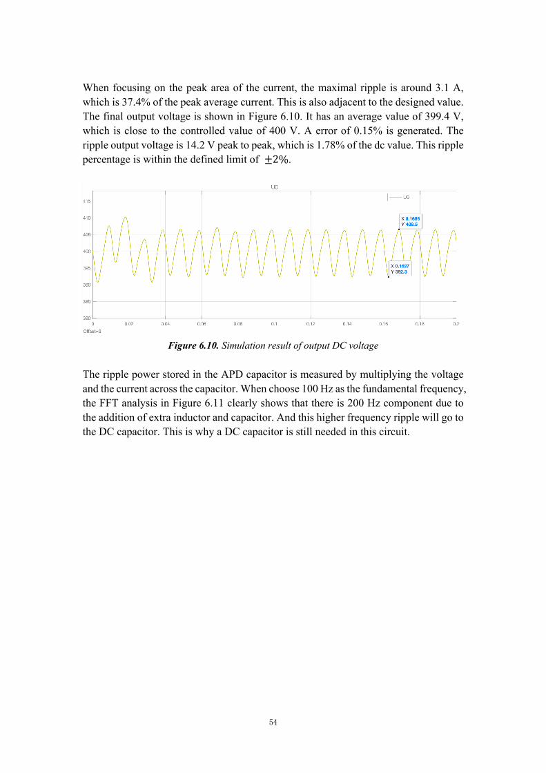
54
When focusing on the peak area of the current, the maximal ripple is around 3.1 A, which is 37.4% of the peak average current. This is also adjacent to the designed value. The final output voltage is shown in Figure 6.10. It has an average value of 399.4 V, which is close to the controlled value of 400 V. A error of 0.15% is generated. The ripple output voltage is 14.2 V peak to peak, which is 1.78% of the dc value. This ripple percentage is within the defined limit of ±2%.
Figure 6.10. Simulation result of output DC voltage
The ripple power stored in the APD capacitor is measured by multiplying the voltage and the current across the capacitor. When choose 100 Hz as the fundamental frequency, the FFT analysis in Figure 6.11 clearly shows that there is 200 Hz component due to the addition of extra inductor and capacitor. And this higher frequency ripple will go to the DC capacitor. This is why a DC capacitor is still needed in this circuit.
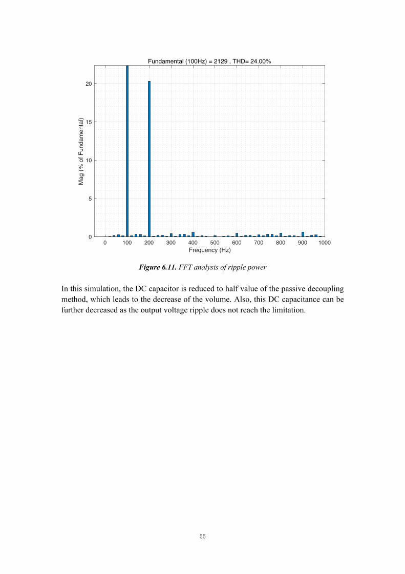
55
Figure 6.11. FFT analysis of ripple power
In this simulation, the DC capacitor is reduced to half value of the passive decoupling method, which leads to the decrease of the volume. Also, this DC capacitance can be further decreased as the output voltage ripple does not reach the limitation.
Fundamental (100Hz) = 2129 , THD= 24.00%
0 100 200 300 400 500 600 700 800 900 1000Frequency (Hz)
0
5
10
15
20M
ag (%
of F
unda
men
tal)
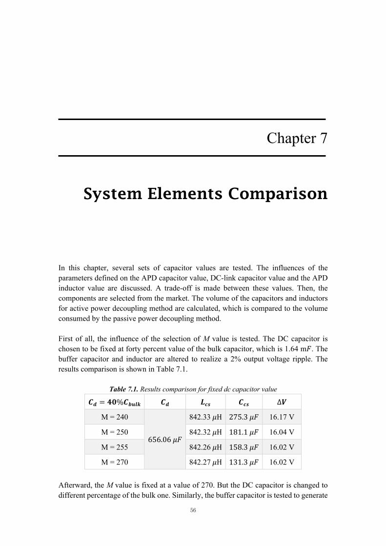
56
Chapter 7
System Elements Comparison
In this chapter, several sets of capacitor values are tested. The influences of the parameters defined on the APD capacitor value, DC-link capacitor value and the APD inductor value are discussed. A trade-off is made between these values. Then, the components are selected from the market. The volume of the capacitors and inductors for active power decoupling method are calculated, which is compared to the volume consumed by the passive power decoupling method. First of all, the influence of the selection of M value is tested. The DC capacitor is chosen to be fixed at forty percent value of the bulk capacitor, which is 1.64 m𝐹. The buffer capacitor and inductor are altered to realize a 2% output voltage ripple. The results comparison is shown in Table 7.1.
Table 7.1. Results comparison for fixed dc capacitor value
𝑪𝒅 = 𝟒𝟎%𝑪𝒃𝒖𝒍𝒌 𝑪𝒅 𝑳𝒄𝒔 𝑪𝒄𝒔 ∆𝑽
M = 240
656.06𝜇𝐹
842.33𝜇H 275.3𝜇𝐹 16.17 V
M = 250 842.32𝜇H 181.1𝜇𝐹 16.04 V
M = 255 842.26𝜇H 158.3𝜇𝐹 16.02 V
M = 270 842.27𝜇H 131.3𝜇𝐹 16.02 V Afterward, the M value is fixed at a value of 270. But the DC capacitor is changed to different percentage of the bulk one. Similarly, the buffer capacitor is tested to generate
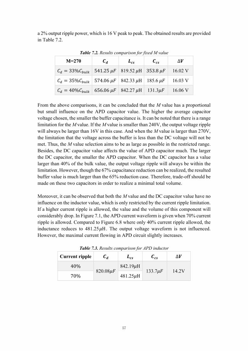
57
a 2% output ripple power, which is 16 V peak to peak. The obtained results are provided in Table 7.2.
Table 7.2. Results comparison for fixed M value
M=270 𝑪𝒅 𝑳𝒄𝒔 𝑪𝒄𝒔 ∆𝑽
𝐶6 = 33%𝐶()*+ 541.25𝜇𝐹 819.52𝜇H 353.8𝜇𝐹 16.02 V
𝐶6 = 35%𝐶()*+ 574.06𝜇𝐹 842.33𝜇H 185.6𝜇𝐹 16.03 V
𝐶6 = 40%𝐶()*+ 656.06𝜇𝐹 842.27𝜇H 131.3𝜇𝐹 16.06 V
From the above comparisons, it can be concluded that the M value has a proportional but small influence on the APD capacitor value. The higher the average capacitor voltage chosen, the smaller the buffer capacitance is. It can be noted that there is a range limitation for the M value. If the M value is smaller than 240V, the output voltage ripple will always be larger than 16V in this case. And when the M value is larger than 270V, the limitation that the voltage across the buffer is less than the DC voltage will not be met. Thus, the M value selection aims to be as large as possible in the restricted range. Besides, the DC capacitor value affects the value of APD capacitor much. The larger the DC capacitor, the smaller the APD capacitor. When the DC capacitor has a value larger than 40% of the bulk value, the output voltage ripple will always be within the limitation. However, though the 67% capacitance reduction can be realized, the resulted buffer value is much larger than the 65% reduction case. Therefore, trade-off should be made on these two capacitors in order to realize a minimal total volume. Moreover, it can be observed that both the M value and the DC capacitor value have no influence on the inductor value, which is only restricted by the current ripple limitation. If a higher current ripple is allowed, the value and the volume of this component will considerably drop. In Figure 7.1, the APD current waveform is given when 70% current ripple is allowed. Compared to Figure 6.8 where only 40% current ripple allowed, the inductance reduces to 481.25𝜇H . The output voltage waveform is not influenced. However, the maximal current flowing in APD circuit slightly increases.
Table 7.3. Results comparison for APD inductor
Current ripple 𝑪𝒅 𝑳𝒄𝒔 𝑪𝒄𝒔 ∆𝑽
40% 820.08𝜇𝐹
842.19𝜇H 133.7𝜇𝐹 14.2V
70% 481.25𝜇H
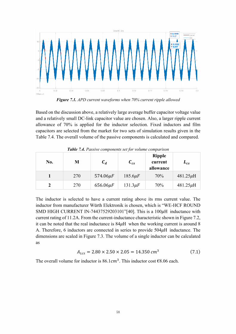
58
Figure 7.1. APD current waveforms when 70% current ripple allowed
Based on the discussion above, a relatively large average buffer capacitor voltage value and a relatively small DC-link capacitor value are chosen. Also, a larger ripple current allowance of 70% is applied for the inductor selection. Fixed inductors and film capacitors are selected from the market for two sets of simulation results given in the Table 7.4. The overall volume of the passive components is calculated and compared.
Table 7.4. Passive components set for volume comparison
No. M 𝑪𝒅 𝑪𝒄𝒔 Ripple current
allowance 𝑳𝒄𝒔
1 270 574.06𝜇𝐹 185.6𝜇𝐹 70% 481.25𝜇H
2 270 656.06𝜇𝐹 131.3𝜇𝐹 70% 481.25𝜇H The inductor is selected to have a current rating above its rms current value. The inductor from manufacturer Würth Elektronik is chosen, which is “WE-HCF ROUND SMD HIGH CURRENT IN-74437529203101”[40]. This is a 100𝜇H inductance with current rating of 11.2A. From the current-inductance characteristic shown in Figure 7.2, it can be noted that the real inductance is 84𝜇H when the working current is around 8 A. Therefore, 6 inductors are connected in series to provide 504𝜇H inductance. The dimensions are scaled in Figure 7.3. The volume of a single inductor can be calculated as
𝐴-,. = 2.80 × 2.50 × 2.05 = 14.350𝑐𝑚± (7.1)
The overall volume for inductor is 86.1𝑐𝑚±. This inductor cost €8.06 each.
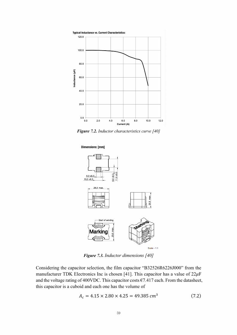
59
Figure 7.2. Inductor characteristics curve [40]
Figure 7.3. Inductor dimensions [40]
Considering the capacitor selection, the film capacitor “B32526R6226J000” from the manufacturer TDK Electronics Inc is chosen [41]. This capacitor has a value of 22𝜇F and the voltage rating of 400VDC. This capacitor costs €7.417 each. From the datasheet, this capacitor is a cuboid and each one has the volume of
𝐴, = 4.15 × 2.80 × 4.25 = 49.385𝑐𝑚± (7.2)
60
For comparison set No.1 and No.2, nine and six capacitors are needed to connect in parallel to support the required APD capacitance. This requires the volume of 444.465𝑐𝑚± and 296.31𝑐𝑚± respectively. And for the DC capacitor, if the same component is used, 26 and 30 capacitors are needed separately. It can be realized that set No.2 has a smaller volume.
Table 7.5. Overall volume comparison
No. 𝑪𝒅 𝑪𝒄𝒔 𝑳𝒄𝒔 Overall Total cost
1 1284.01𝑐𝑚± 444.465𝑐𝑚± 86.1𝑐𝑚± 1863.96𝑐𝑚± €315.372
2 1481.55𝑐𝑚± 296.31𝑐𝑚± 86.1𝑐𝑚± 1814.575𝑐𝑚± €307.955 When the passive power decoupling method is applied, a bulk capacitor of 1.64mF should be used. Seven “C4DEFPQ6260A8TK” capacitors from KEMET are used for filtering [42]. This capacitor has a volume of
𝐴()*+ = 8.401 × 6.60 = 465.696𝑐𝑚± (7.3)
The DC capacitor volume will be 3259.972𝑐𝑚± in total. Each unit cost €80.98, which leads to a total cost of €566.86. Comparing the active power decoupling method to the conventional one, the volume of the active one decreases to 55.66% of the latter one. The cost reduces to 54.32% of the conventional method.
61
Chapter 8
Conclusion and Future work
8.1 Conclusion This project focus on the AC on-board charging technology of the electrical vehicles. The main challenge of this technology concerns the passive components applied for second-order ripple energy filtering. Active power decoupling method is raised to realize a compact and high power density charging system. Electrolytic-less capacitors are implemented to ensure long battery lifetime. At the beginning, the background knowledge about the electrical vehicle market and three level charging technologies current existing were reviewed. Then, different types of capacitors involving in the power decoupling function were reviewed and discussed. After that, the research oriented to the AC on-board charging technology was identified. The AC charger was constructed by a single-phase AC-DC rectifier with an added active power decoupling circuit. Different types of active power decoupling circuits were discussed, and relevant literature was reviewed. Next, the charging system with buck-type active power decoupling module was analytically modeled. In this part, the minimal value for DC capacitor is firstly determined for the passive power decoupling method. Secondly, the power distribution of the charging system is mathematically analyzed when an active power decoupling method is used. Thirdly, the determination of the energy storage elements was provided, which is a function of several factors. The influences of each factor were verified. Afterwards, a simulation model based on this mathematical analysis was built in Simulink. The simulated results were verified with the theoretical one, showing good accuracy. Finally, several commercial passive components for implementation were selected, which proved a possible reduction of approximately half can be achieve in both volume and cost.

62
8.2 Future work In this thesis, the charging system is mathematically analyzed and simulated based on the buck-type active power decoupling circuit. However, other types of active decoupling module are briefly discussed in Chapter 4.2. It is interested to identify the practical system performance if these modules are applied. In the future, the simulation model should be modified to the single-phase rectifier with the boost-type, buck-boost-type and the split type power buffer. Benchmark of different APD topologies should be made. Apart from that the possible achieved volume and cost merits, the system losses should also be calculated. Zero voltage switching should also be considered for analysis for the active power decoupling circuits in order to diminish the losses across the switches. Finally, hardware prototype should be tested and compared to the simulation results.
63
Reference [1] “Nissan LEAF 2019: 100% elektrische auto,” Nissan. [Online]. Available: https://www.nissan.nl/voertuigen/nieuw/leaf.html. [Accessed: 08-Apr-2020]. [2] IEA, “Global EV Outlook 2019 – Analysis,” IEA. [Online]. Available: https://www.iea.org/reports/global-ev-outlook-2019. [Accessed: 27-Jan-2020]. [3] “The Global Electric Vehicle Market In 2019 – Virta,” Virta Global. [Online]. Available: https://www.virta.global/global-electric-vehicle-market. [Accessed: 27-Jan-2020]. [4] “Global EV Sales for the 1st Half of 2019,” EV. [Online]. Available: http://www.ev-volumes.com/country/total-world-plug-in-vehicle-volumes/. [Accessed: 27-Jan-2020]. [5] W. Li, R. Long, and H. Chen, “Consumers’ evaluation of national new energy vehicle policy in China: An analysis based on a four paradigm model,” Energy Policy, vol. 99, pp. 33–41, 2016. [6] G. Harrison and C. Thiel, “An exploratory policy analysis of electric vehicle sales competition and sensitivity to infrastructure in Europe,” Technological Forecasting and Social Change, vol. 114, pp. 165–178, 2017. [7] K. Y. Bjerkan, T. E. Nørbech, and M. E. Nordtømme, “Incentives for promoting Battery Electric Vehicle (BEV) adoption in Norway,” Transportation Research Part D: Transport and Environment, vol. 43, pp. 169–180, 2016. [8] K. Palmer, J. E. Tate, Z. Wadud, and J. Nellthorp, “Total cost of ownership and market share for hybrid and electric vehicles in the UK, US and Japan,” Applied Energy, vol. 209, pp. 108–119, 2018.
64
[9] Y. Zhou, M. Wang, H. Hao, L. Johnson, H. Wang, and H. Hao, “Plug-in electric vehicle market penetration and incentives: a global review,” Mitigation and Adaptation Strategies for Global Change, vol. 20, no. 5, pp. 777–795, 2014. [10] Infinity Research, “Tesla's Largest Competitive Advantage,” Seeking Alpha, 06-Feb-2019. [Online]. Available: https://seekingalpha.com/article/4238584-teslas-largest-competitive-advantage. [Accessed: 27-Feb-2020]. [11] R. Salvucci, J. Tattini, “Global outlook for the transport sector in energy scenarios,” Transforming Urban Mobility, p. 21, 2019. [12] J. Guo, X. Zhang, F. Gu, H. Zhang, and Y. Fan, “Does air pollution stimulate electric vehicle sales? Empirical evidence from twenty major cities in China,” Journal of Cleaner Production, vol. 249, p. 119372, 2020. [13] J. Zheng, X. Sun, L. Jia, and Y. Zhou, “Electric passenger vehicles sales and carbon dioxide emission reduction potential in China’s leading markets,” Journal of Cleaner Production, vol. 243, p. 118607, 2020. [14] X. Gong, J. Rangaraju, “Taking charge of electric vehicles-both in the vehicle and on the grid,” Texas Instruments, Dallas, TX, USA, p.1-13, 2018. [15] A. S. Al-Ogaili, I. B. Aris, R. Verayiah, A. Ramasamy, M. Marsadek, N. A. Rahmat, Y. Hoon, A. Aljanad, and A. N. Al-Masri, “A Three-Level Universal Electric Vehicle Charger Based on Voltage-Oriented Control and Pulse-Width Modulation,” Energies, vol. 12, no. 12, p. 2375, 2019. [16] M. Yilmaz and P. T. Krein, “Review of Battery Charger Topologies, Charging Power Levels, and Infrastructure for Plug-In Electric and Hybrid Vehicles,” IEEE Transactions on Power Electronics, vol. 28, no. 5, pp. 2151–2169, 2013. [17] “feel the drive ,” EV Solutions | Electric Vehicle Charging Products & Services. [Online]. Available: https://www.evsolutions.com/. [Accessed: 07-Sep-2019]. [18] I. Poole, “Capacitor Types - descriptions of the differnet types of capacitor,” Electronics Notes, 10-Jan-2020. [Online]. Available: https://www.electronics-notes.com/articles/electronic_components/capacitors/capacitor-types.php. [Accessed: 27-Jan-2020]. [19] A. Shaik, Electrolytic capacitor. [Online]. Available: https://www.physics-and-radio-electronics.com/electronic-devices-and-circuits/passive-components/capacitors/electrolyticcapacitor.html. [Accessed: 27-Jan-2020].
65
[20] “Types of Capacitor and their Construction,” Basic Electronics Tutorials, 10-Jul-2018. [Online]. Available: https://www.electronics-tutorials.ws/capacitor/cap_2.html. [Accessed: 27-Jan-2020]. [21] A. Martin, M. Davis-Marsh, G. Pinto and I.Jorio, “Capacitor selection for DC/DC converters: What you need to know to prevent early failures, and reduce switching noise,” Santa Clara, California, USA: TI–Silicon Valley Analog, 2012. [22] V. F. Pires, J. Monteiro, A. Cordeiro, and J. F. Silva, “Integrated Battery Charger for Electric Vehicles Based on a Dual-Inverter Drive and a Three-Phase Current Rectifier,” Electronics, vol. 8, no. 10, p. 1199, 2019. [23] C. Shi, Y. Tang and A. Khaligh, "A Three-Phase Integrated Onboard Charger for Plug-In Electric Vehicles," in IEEE Transactions on Power Electronics, vol. 33, no. 6, pp. 4716-4725, June 2018. [24] M. M. Morcos, N. G. Dillman and C. R. Mersman, "Battery chargers for electric vehicles," in IEEE Power Engineering Review, vol. 20, no. 11, pp. 8-11, Nov. 2000. [25] J. Lee, "An EL Capacitorless EV On-Board Charger Using Harmonic Modulation Technique," in IEEE Transactions on Industrial Electronics, vol. 61, no. 4, pp. 1784-1787, April 2014. [26] K. Yoo, K. Kim and J. Lee, "Single- and Three-Phase PHEV Onboard Battery Charger Using Small Link Capacitor," in IEEE Transactions on Industrial Electronics, vol. 60, no. 8, pp. 3136-3144, Aug. 2013. [27] A. Khaligh and S. Dusmez, "Comprehensive Topological Analysis of Conductive and Inductive Charging Solutions for Plug-In Electric Vehicles," in IEEE Transactions on Vehicular Technology, vol. 61, no. 8, pp. 3475-3489, Oct. 2012. [28] M. Vasiladiotis and A. Rufer, "Dynamic Analysis and State Feedback Voltage Control of Single-Phase Active Rectifiers With DC-Link Resonant Filters," in IEEE Transactions on Power Electronics, vol. 29, no. 10, pp. 5620-5633, Oct. 2014. [29] Y. Sun, Y. Liu, M. Su, W. Xiong, and J. Yang, “Review of Active Power Decoupling Topologies in Single-Phase Systems,” IEEE Transactions on Power Electronics, pp. 1–1, 2015. [30] J. L. Lesle, R. Caillaud, F. Morel, N. Degrenne, C. Buttay, R. Mrad, C. Vollaire, and S. Mollov, “Optimum design of a single-phase Power Pulsating Buffer (PPB) with PCB-integrated inductor technologies,” 2018 IEEE International Conference on Industrial Technology (ICIT), 2018.
66
[31] K.-H. Chao, P.-T. Cheng, and T. Shimizu, “New control methods for single phase PWM regenerative rectifier with power decoupling function,” 2009 International Conference on Power Electronics and Drive Systems (PEDS), 2009. [32] R. Wang, F. Wang, D. Boroyevich, R. Burgos, R. Lai, P. Ning, and K. Rajashekara, “A High Power Density Single-Phase PWM Rectifier With Active Ripple Energy Storage,” IEEE Transactions on Power Electronics, vol. 26, no. 5, pp. 1430–1443, 2011. [33] H. Li, K. Zhang, and H. Zhao, “Active DC-link power filter for single phase PWM rectifiers,” 8th International Conference on Power Electronics - ECCE Asia, 2011. [34] H. -. Chae, H. -. Moon and J. -. Lee, "On-board battery charger for PHEV without high-voltage electrolytic capacitor," in Electronics Letters, vol. 46, no. 25, pp. 1691 -1692, 9 December 2010. [35] A. C. Kyritsis, N. P. Papanikolaou and E. C. Tatakis, "A novel Parallel Active Filter for Current Pulsation Smoothing on single stage grid-connected AC-PV modules," 2007 European Conference on Power Electronics and Applications, Aalborg, pp. 1-10, 2007. [36] P. T. Krein, R. S. Balog and M. Mirjafari, "Minimum Energy and Capacitance Requirements for Single-Phase Inverters and Rectifiers Using a Ripple Port," in IEEE Transactions on Power Electronics, vol. 27, no. 11, pp. 4690-4698, Nov. 2012. [37] Z. Qin, Y. Tang, P. C. Loh, and F. Blaabjerg, “Benchmark of AC and DC active power decoupling circuits for second-order harmonic mitigation in kW-scale single-phase inverters,” 2015 IEEE Energy Conversion Congress and Exposition (ECCE), 2015. [38] D. Kim, M. Kim and B. Lee, "An Integrated Battery Charger With High Power Density and Efficiency for Electric Vehicles," in IEEE Transactions on Power Electronics, vol. 32, no. 6, pp. 4553-4565, June 2017. [39] M. Qiu, P. Wang, H. Bi, and Z. Wang, “Active Power Decoupling Design of a Single-Phase AC–DC Converter,” Electronics, vol. 8, no. 8, p. 841, 2019. [40] Würth Elektronik, “Datasheet - WE-HCF Round Wire SMT High Current Inductor,” 74437529203101, March 2020. [41] TDK Electronics Inc, “Datasheet - CAP FILM 22UF 5% 400VDC RADIAL,” B32526R6226J000, June 2018.

67
[42] KEMET, “Datasheet - CAP FILM 260UF 10% 400VDC RADIAL,” C4DEFPQ6260A8TK. [Online] Available: https://content.kemet.com/datasheets/F3 303_C4DE.pdf [Accessed April 2020]
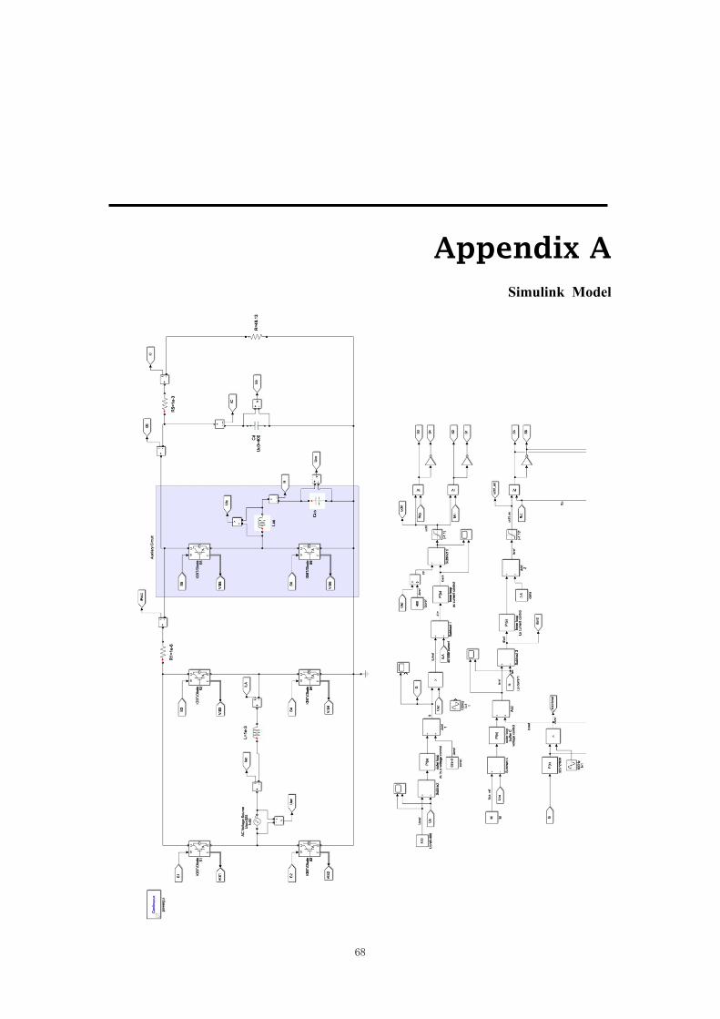
68
Appendix A Simulink Model

69
Appendix B Initial Transcript for Simulink


