Embed Size (px)
Citation preview
TM 11-261/TO 16-35CJ731-15
This manual supersedes so much of TM 11-278,23 October 1946, including C 1,12 November 1947; C 2,14 April 1948; and C 3, 17 February 1949; as pertains to Dual Diversity Converters CV-31jTRA-7 and CV-31AjTRA-7
DUAL DIVERSITY CONVERTERS
CV-31JTRA-7, CV-31AJTRA-7
CV-31 BjTRA-7, CV-31CjTRA-7
AND CV-31D/TRA-71
I
--~-;--------,.-------------------------,.--
United States Government Printing Office
Washington: 1952
Iii ilH· 1;1
ii
-DEPARTMENTS OF THE ARMY AND THE AIR FORCE
WASHINGTON 25, D.C., 11 June 1952
TM 11-261/TO 16-35CV31-15 is published for the information and guidance of all concerned.
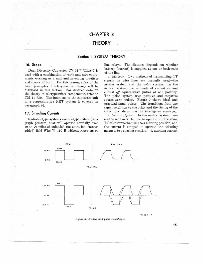
[AU 413.44 (28 May 52)]
By ORDER OF .THE SECRETARIES OF THE ARMY AND THE AIR FORCE:
OFFICIAL:
WM. E. BERGIN Major General, USA The Adjutant General
OFFICIAL:
K. E. THIEBAUD Colonel, USAF Air Adjutant General
DISTRIBUTION:
Active Army:
J. LAWTON COLLINS Chief of Staff, United States Army
N. F. TWINING Acting Chief of Staff, United States Air Force
Tech Svc (1); Tech Svc Bd (1); AFF Bd (ea Svc Test Sec) (1); AFF (5); AA Comd (2); OS Maj Comd (5); Base Comd (5); Log Comd (5);A (20); MDW (5); CHQ (2); FT (2); Sch (5) except 11 (25); Gen Dep (2); Dep 11 (20) except Sig Sec, Gen Dep(10); Tug Div (2); POE (10), OSD (2); Lab 11 (5); Mil Dist (3); 4th & 5th Ech Maint Shops 11 (3); Two (2) copies to each of the following T/O & E's: 11-107; 11-127; H-500 CA, CB, CC, CD; 11-587; 11-592; 11-597.
NG: Same as Active Army except one copy to each unit. ORC: Same as Active Army except one copy to each unit. For explanation of distribution formula, see SR 310-90-1.
/
CONTENTS
CHAPTER 1. INTRODUCTION Paragraph Page
Section I. GeneraL ___________________________________________________________________ _ 1,2 1 II. Description and data ___________ - ~ ~ - - - - __ - __ - - - - - - - - - -. - _ - - - - - - - - - - ________ - - - _ 3-8 1-4
CHAPTER 2. ORGANIZATIONAL MAINTENANCE INSTRUGIONS Section I. Preventive maintenance services ______________________________________________ _ 9-12 lO
II. Lubrication and weatherproofing _____________ .: ________________________________ _ 13-15 13-14
CHAPTER 3. THEORY Section I. System theory _______________________________________________________ c ______ _ 16-22 15-19
II. Theory of dual diversity converter ____________________________________________ _ 23-32 21-36 III. Power supply and tone oscillator _______________ . _______________________________ _ 33-39 38-44
CHAPTER 4. FIELD MAINTENANCE INSTRUCTIONS Section I. Trouble shooting at field maintenance leveL ____________________________________ _ 40-46 46-53
II. Itepairs _______________________________________________ ~ ___________________ ~_ 47.,.49 67-68 III. Maintenance and repair of relay K40L ____ -- __________________________________ _ 50-54 69-75 IV. Alinement __________________________________ - __________________________ . _____ _ 55-57 76-81
V. Final testing _______________________________________________________________ _ 58-71 82-88
CHAPTER 5, SHIPMENT AND LIMITED STORAGE AND DEMOLITION TO PREVENT ENEMY' USE Section I. Shipment and limited storage ____________ .: ____________________________________ _ 72, 73 92
II. Demolition of materiel to prevent enemy use ___________________________________ _ 74, 75 92
APPENDIX I. REFERENCES_ -- - - - - - - - - - - - - - - -- - - - - -" - - - - -- - - - - - - - - - - -- --- - -- - - - - - - _ -_ - _ - --- 93 II. IDENTIFICATION TABLE OF PARTS ___________ :.. _______________________________ _ 96
<iLOSSARY-- ____________________________________________ ------------------------------- 112 INDEX _________________________________________________ ---------------------------- ____ _ 120
jii
-<,;...~~~--~~---_r__TTT'IT11I"I_""I''''TI· ----------------~~-/

l'I":I'i
SAFETY NOTICE Voltages as high as 675 volts are used in the operation of this equipment.
These voltages are dangerous to life. Do not change tubes or make adjustments inside the set with the AC SUPPLY switch ON. A few service checks must be made inside the set with the high voltage on. When making these checks, always have present another person capable of rendering aid. Keep one hand in your pocket while making high-voltage measurements. This precaution will prevent touching the electrical circuit with more than one part of the body at one time.
iii I,ll ,II i
v
vi
RESCUE.
In case of electric shock, shut off the high voltage at once and ground the circuits. If the high voltage cannot be turned off without delay, free the victim from contact with the live conductor as promptly as possible~ Avoid direct contact with either the live conductor or the victim's body. Use a dry board, dry clothing, or other nonconductor to free the victim. An ax may be used to cut the high-voltage wire. Use extreme caution to avoid the resulting electric flash.
SYMPTOMS.
a. Breathing stops abruptly in electric shock if the current passes through the breathing center at the' base of the brain. If the shock has not been too severe, the breath center recovers after a while and normal breathing is resumed, provided that a sufficient supply of air has been furnished meanwhile by artificial respiration.
b. The victim is usually very white or blue. The pulse is very weak or entirely absent and unconsciousness is complete. Burns are usually present. The victim's body may become rigid or stiff in a very few minutes .. This condition is due to the action of electricity and is not to be considered rigor mortis. Artificial respiration must still be given, as several such cases are reported to have recovered. The ordinary and general tests for death should never be accepted.
TREATMENT.
a. Start artificial respiration immediately_ At the same time send for a medical officer, if assistance is available. Do not leave the victim unattended. Perform artificial respiration at the scene of the accident, unless the victim's or operator's life is endangered from such action. In this case only, remove the victim to another location, but no farther than is necessary for safety. If the new location is more
than a few feet away, artificial respiration should be given while the victim is being It:loved. If the method of transportation prohibits the use of the Shaeffer .prone pressure method, other methods of resuscitation may be used. Pressure may be exerted on the front of the victim's diaphragm, or the direct mouth-to-mouth method may be used. Artificial respiration, once started, must be continued, without loss of rhythm.
b. Lay tHe victim in a prone position, one arm extended directly overhead, and the other arm bent at the elbow so that the back of the hand supports the head. The face should be turned away from the bent elbow so that the nose and mouth are free for breathing.
c. Open the victim's mouth and remove any foreign bodies, such as false teeth, chewing gum, or tobacco. The mouth should remain open, with the tongue extended. Do not permit the victim to draw his tongue back into his mouth or throat. .
d. If an assistant is available during resuscitation, he should loosen any tight clothing to permit free circulation of blood and to prevent restriction of breathing. He should see that the. victim is kept warm, by applying blankets or other covering, or by applying hot rocks or bricks wrapped in cloth or paper to prevent injury to the victim. The assistant should also be ever watchful to see that the victim does not swallow his tongue. He should continually wipe from the victim's mouth any frothy mucus or saliva that may collect and interfere with respiration.
e. The resuscitating operator should straddle the victim's thighs, or one leg, in such manner that:
(1) the operator's arms and thighs will be vertical while applying pressure on the small of the victim's back;
(2) the operator's fingers are in a natural position on the victim's back with the little finger lying on the last rib;
(3) the heels of the hands rest on either side of the spine as far apart as convenient without allowing the hands to slip off the victim;
(4) the operator's elbows are straight and locked.
f. The resuscitation procedure is as follows: (1) Exert downward pressure, not exceeding
60 pounds, for 1 second. (2) Swing back, suddenly releasing pressure,
and sit up on the heels. (3) After 2 seconds rest, swing forward again,
positioning the hands exactly as before, and apply pressure for another second.
g. The forward swing, positioning of the hands, and the downward pressure should be accompli!;hed in one continuous motion, which requires 1 second. The release and backward swing require 1 second. The addition of the 2·second rest makes a total of 4
TL 15338-0
A
A. CORRECT POSITION. Operator's elbows straight and locked. Victim's face turned away from bent elbow and resting on back of hand.
I. FORWARD SWING AND POSITIONING OF HANDS. Little finger rests on last rib.
C. DOW N W A If D PRESSURE. Arms and thighs vertical.
D. REST POSITION. releases
pressure suddenly, swings back on heels, and resls for 2 seconds.
se~onds for a complete cycle. Until the operator is thoroughly famiiiar with the correct cadence of the cycle, he should count the seconds aloud, speaking distinctly and counting evenly in thousands. Example:, one thousand and one, one thousand an.d two, etc.
h. Artificial respiration should be continued until the ,victim regains nonnal breathing or is pronounced dea\i by a medical officer. Since it may be necessary to continue resuscitation for several hoUrs, relief operators should be used if available.
RELIEVING OPERATOR.
The relief operator kneels beside the operator and follows him through several complete cycles. When the relief operator is s\lre he has the correct rhythm, he places his hands on the. operator's hands without applying pressure. This indicates that he is ready to take over. On the backward swing, the operator moves and the relief operator takes his position. The relieved operator follows through several complete cycles to be sure that the new operator has the correct rhythm. He remains alert to take over instantly if the new operator falters or hesitates on the cycle.
STIMULANTS.
ct. !fan, inhalant stimulant is used, such as aro-
111I11Hlli:1I1111
matic spirits of ammonia, the individual administer-" ing the stimulant should first test it himself· to see how close he can hold the inhalant to his own nostril for comfortable breathing. Be sure that the inhalant is not held any closer to the victim's nostrils, and then for only 1 or 2 seconds every minute. ,
b. After the victim has regained consciousness, he may be given hot coffee, hot tea, or a glass of water containing ¥.! teaspoon of aromatic spirits of ammonia. Do not give a.ny liquids to a.n unconscious victim.
CAUTIONS.
a. After the victim revives, keep him LYING QUIETLY. Any injury a person may have received may cause a condition of shock. Shock is present if the victim is pale and has a cold sweat, his pulse is weak and rapid, and his breathing is short and gasping.
b. keep the' victim lying flat on his back, with hjs head lower than the rest of his body and his hips elevated. Be sure that there is no tight clothing to restrict the free 'circulation of blood or hinder natural breathing. Keep him warm' and quiet.
c. A resuscitated victim must be watched ~are· fully as he may suddenly stop breathing. Never leave a, resuscitat6'1i person alone unUlit is GER· T AIN that he is fuZZy conscious and breathing nor-mally. TL U5338-E
vii
Figure 1. Dual Diversity Converter CV-31 D/ TRA-7, front view.
viii
,"
TM8 man!lal8upersedes 80 much of TM 11-278;23 Oct()~eT}lJ4{J,including Cl, 12 November 1947; C2, 14 April 1948; and C3, 17 February 1949; a8 pertains to Dual Diversity Converters CV-31/TRA-7and-CV-31A/TRAI-7,
CHAPTER I
INTRODUCTION
Section I.' GENERAL
1. Scope a. This manual contains a description of Dual
Diversity Converter OV-31(*)/TRA~7 and its operating controls, a chapter on theory of operation, and instructions for field maintenance -and repair of the equipment. In addition, this manual .contains two appendixes covering a list of references and an identification table of parts.
b. Since the converter unit is normally installed in one of several different systems, installation and operation instructions are omitted from this manual and are included in the technical manuals . covering the particular system. Specialized organizational maintenance information, such as techniques for isolating trouble to the particular system unit, are also omitted from this manual and included in the various systems manuals.
c. Official nomenclature followed by (*) is used tp indicate all models of the item of equipment discussed in this manuaL For -example, Dual
-Diversity Oonverter OV-31(*)/TRA-7 indicates Dual Diversity Converters CV-31/TRA-7, OV-
_ 31A/TRA-7, OV-31B/TRA-7, OV-31O/TRA-7, and CV-31D/TRA-7 (fig. 1). Rectifier Power Unit PP-193(*)/TRA-7 and Oscillator 0--41(*)/ TRA-7 were not nomenclatured separately when issued with Dual Diversity Converter OV-31/ TRA-7; but do have separate nomenclature in the A through D models and, retroactively, in the basic modeL
2. Forms and Records The following forms will be used for reporting
unsatisfactory conditions of Army materiel and equipment.
a. DD Form 6, Report of Damaged or Improper Shipment, will be filled out and forwarded as prescribed in SR 745--45-5 (Army), NAV DEPT SERIAL 85POO (Navy), and AFR 71--4 (Air Force).
b. DA Form 468, Unsatisfactory Equipment Report, will be filled out and forwarded to the Office of the Ohief Signal Officer as prescribed in SR 700--45-5.
c. USAF Form 54, Unsatisfactory Report, will be filled out and forwarded to Oommanding General, Air Materiel Oommand, Wright-Patterson Air Force Base, Dayton, Ohio, as prescribed in SR 700--45-5 and AFR 65-26.
d. DA AGO Form 11-238, Operator First Echelon Maintenance Oheck List for Signal Corps Equipment (Radio Communication, Direction Finding, Oarrier, Radar), will be prepared in accordance with instructions on the back of the form.
e. DA AGO Form 11-239, Second and Third Echelon Maintenance Oheck List for Signal Corps Equipment- (Radio Oommunication, Direction Finding, Carrier, Radar), will be prepared in accordance with instructions on the back of the form.
f. Use other forms and records as authorized.
Section II. DESCRIPTION AND DATE
3. Purpose and Use
. a. Dual Diversity Oonverter OV-31(*)jTRA-7 is a unit used in conjunction with two radio receivers (designated as Receiver A and Receiver B) at an RTT (radioteletype) terminal. The
210961-52-2
11111l1li1111111
i-f (intermediate-frequency) output of these receivers is fed to the dual diversity converter unit, which converts it into polar and neutral d-c (direct-current), TT (teletypewriter), or telegraph signals. One of the features of the output circui~ is the frequency-drift compensator, which is con-
1
trolled by theDRIFT COMPENSATOR switch. The compensator cir.cuit tends to minimize the signal bias (wave£or1ll distortion) if the received signals drift away from normal.
b. The converter unit has self-contained meters for measuring various currents and voltages throughout the unit. The d-c output circuit in the converter includes amplifiers and controls to produce unbiased TT or telegraph signals for
"transmission over local loops or extension circuits. Either polar or neutral loop operation is possible. The converter unit also has facilities to permit reversing the polarities of the output mark and space' signals, and for establishing test mark and space Qlltput sigilals for adjustment purposes.
4. System Application a. Dual Diversity Converter CV-31(*)jTRA-
7 is a unit of radioteletype equipment housed in either one 'or three shelters which comprise a medium or high-powered, mobile RTT terminal. Two RTT terminals operating together provide full-duplex, half-duplex, or one-way reversible teletypewriter operation. Emergency FS (frequencyshift) or c-w (continuous-wave) code operation is also possible with this equipment.
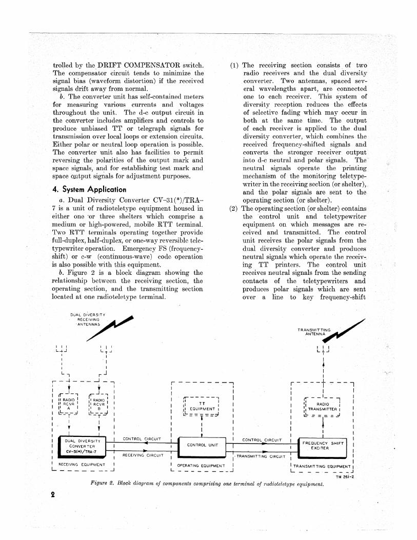
b. Figure 2 is a block diagram showing the relationship between the receiving section, the operating section, and the transmitting section located at one radioteletype terminal.
I
I I
DUAL DI'VERSITY RECEIVING
-ANTENNAS
I I I
Lt-' I
" I I I
L-, rJ
(1) ThereceIvrng section consists .of two radio receivers and the dual diversity converter. Two antennas, spaced' several wavelengths apart, are connected one to each receiver. This system of diversity reception reduces the effects . of selective fading which may occur in both at the same time. The output of each receiver is applied to the dual diversity converter, which combines the received frequency-shifted signals and converts the stronger receiver output into d-c neutral and polar signals. The' neutral signals operate the printing mechanism of the monitoring teletypewriterin the receiving section (or shelter),. and ,the polar signals are sent to. the operating section (or shelter).
(2) The operating section (or shelter) contains the control unit and teletypewriter equipment on which messages are received and transmitted. The control unit receives the polar signals from the dUlil diversity converter and produces neutral signals which operate the receiv-:. ing TT pr~ters. The control unit receives neutral signals from the sending contacts of the teletypewriters and produces polar signals which are sent over aline to key frequency-shift
TRANSMITTING, " "" /. "
ANTENN~
t 1'1 Lt..J
~ I I
r--+----.J--, ", J I
r - -.- - - - --, r - - __ .1 I I
-:----,
I I
n -1-, r.: -., I II RADIO I I RADIO I I II RCVR I II RCVR I II A 1 :1 ,8 I 1 I!- - - .d ,.L - - I -T "--T.J
I I , , I I I
DUAL DIVERSITY I CONVERTER I
CV-3t{*)/TRA-7
I I RECEIVING EQUIPMENT I L _______ ..J
CONTROL CIRCUIT
RECEIVING CIRCUIT
I I I I I :r------l I I II TT I
I II EQUIPMENT I "LL- _'_ - - I
I --1--::7 I I I I I t I I CONTROL UNIT
I
1
I
I I I OPERATING EQUIPMENT I L ________ ...l
CONTROL CIRCUIT
I I I ~ - -1- - '-,
II RADIO I :1 TRANSMITTER I
a!- = =r:.d I
I J I FREQUENCY SHifT I EXCITER
I I I
• TRANSMITTING CIRCUIT :
I I TRANSMITTING' EQ\J1PMENT I L _______ J
TM 26i~2
Figure 2. Block dia,gram of components comprising one terminal of rudioteletype equipment.
2
exciter in the. transmitting section or shelter. For one-way reversible operat~on,' where transmission occurs in onJy one direction at a time, hand-operated key control is provided on tue control unit to permit the operator to disable the transmitter while receiving and to disable the receiver when transmitting. The control unit also is designed to provide for emergency hand-keying of the frequency-shift exciter (FS or c-w signals) from the operating shelter.
(3) The- transmitting section or shelter contains the frequency-shift exciter and the radio transmitter which it excites and controls. The polar signals from the control unit in the operating shelter are applied to the frequency-shift exciter. The nominal carrier frequency, to which the transmitter is set, is that produced by the marking signal. When a spacing signal is received from the control unit, the exciter signal frequency is lowered sufficiently to reduce the transmitter carrier by 850 cycles. The transmitter signal is radiated from the antenna connected to the transmitting shelter.
S. Technical Characteristics Input frequency:
Unlettered, A, B, and 400 to 470 kc (kilocycles). early C. .
Late C and D models __ 440 to 510 kc. Input impedance __________ 108 ohms (approx). Required minimum input 500 uv (m!crovolts).
voltage. Converter intermediate fre
quencies: _ Channel A frequency _ _ _ 50 kc + 425 cycles.
Channel B frequency ___ 29.3 kc +425 cycles. Pass band:
Narrow __ :._ _ _ _ __ _ _ _ _ _ 1,500 cycles. Wide _________ ~ ______ 3,000 cycles. -
Output: NeutraL _____________ Mark .060 ampere. Space
.0 ampere. Polar ________________ Mark + .025 ampere. Space
- .025 ampere. . Number of. tubes ________ '-_ 18. • Power source required ______ U5-volt, 50 to 60 cps cycles
per second). Power consumption ________ 175 watts.
6. Description of Dual Diversity Converter (fig. 1)
I
a .. The converter unit is assembled on a single chassis and is mounted in a metal cabinet equipped
ii,lilliii!
with shock mounts -which make it possible for the equipment to withstand vibration' during transportation. The converter chassis is assem'bled in a cradle which is supported in such a way that, for maintenance and adjustment purposes, it can be pulled out approximately 8 inches from the cabinet. The chassis can be completely removed from the ca.binet by releasing the stop latches on each side of the converter. The converter front panel has two hinged doors. The upper door is held in place by two Dzu8 fasteners and the lower door is kept closed by a single knurled lockscrew. When the upper door is opened, the fuses and transformer connections can be reached. The' lower door conceals adjustment controls and switches which are used in preparing the unit for operation. All connections to the dual diversity converter are made through connectors located at the rear of the unit.
b. The dual diversity converter unit consists of three chassis-the main chassis which contains most of the circuits; a sub chassis (Rectifier Power Unit PP-193(*)/TRA-7) which furnishes all B+, B-, and filament voltages; and another sub chassis (Oscillator 0--41(*)/TRA-7) which provides an audible means of indicating mark and space signals when required.
7. Difference~ in Models a. Dual Diversity Converter CV-31/TRA-7 is
19%2 inches high, 18~ inches deep, 19 inches wide, and weighs 220 pounds. The power unit and the tone oscillator were not nomenclatured individually in this model.
b. Dual Diversity Converter CV-31A/TRA-7 is 25X inches high, 20% inches deep, and 22 inches long (mounted in cabinet). This model includes a disabling switch (SI06) actuated by a cam on the MARK HOLD ,LEVEL adjustment which, when required, serves to make the mark-hold circuit inoperative (fig. 21). After serial number I 203, Order No. 11779-P--48, of the A model, R118 is 47,000 ohms and dual l-uf (microfarad) capacitor C131 has been added.
c. Dual Diversity Converter CV-3IB/TRA-7, when used in Radio Set AN/GRC-26, is mounted in a special cabinet 20% inches high, 17Xe inches deep, and 19X inches long, permitting it to fit into a smaller space. No cradle is used with the special cabinet, 'but the chassis and front panel assembly slides into the cabinet on guard rails and is held in place by eight knurled thumbscrews. The mounting dimensions of several electrical compo-
3
nents have been changed and front panel designations are on an etched aluminum plate. For increased flexibility of connection to other equipment, three additional binding posts are added to the rear of the unit. This model includes the modification of limiter amplifiers V107 and V108 (type 6SJ7 tubes) for improved circuit stability. The modification consists of the addition of resistors R214 and R215 between pin 4 (control grid) and ground of both tubes.
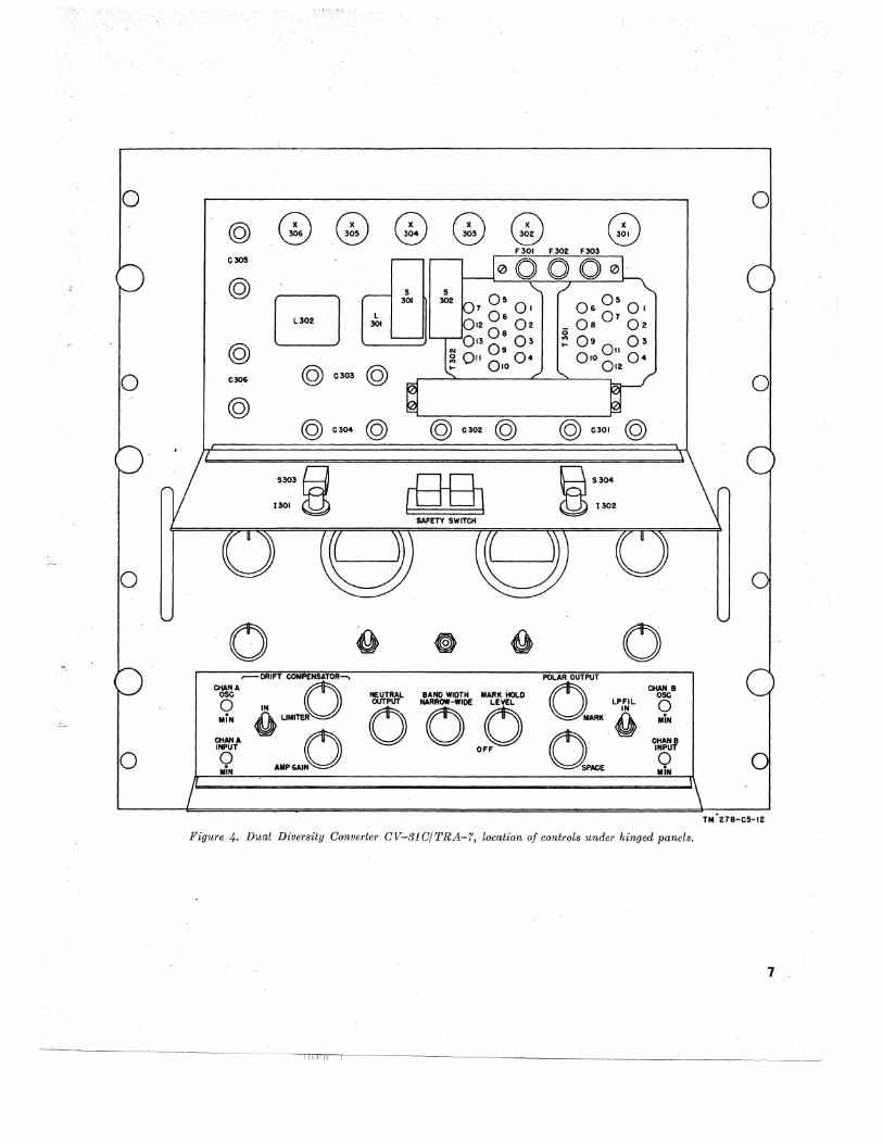
d. Dual Diversity Converter CV-31CjTRA-7 has several additional changes.
(1) Disabling switches for each channel have been added to the front panel immediately below the panel meters. These are labeled CHANNEL A DISABLING (S107) and CHANNEL B DISABLING (S108). Late C models are marked DISABLED and OPERATE.
(2) The input transformer and oscillator network tuning capacitors for each channel (capacitors C101, C103, C105, and C106) have been moved from their chassis loca- . cations and mounted behind the lower hinged door (compare figures 4 and 5).
(3) Resistor R216 (820 ohms) has been added as part of the bias voltage divider for the grid of tube V104.
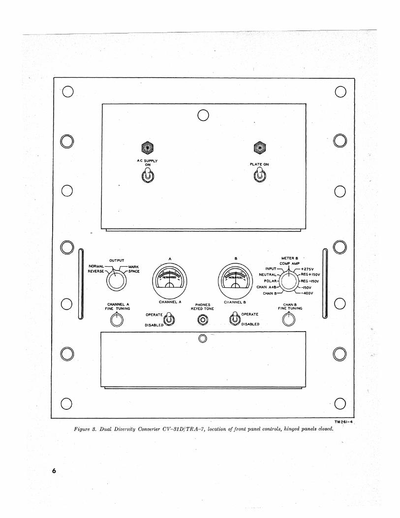
e. Dual Diversity Converter CV-31DjTRA-7 has the CHANNEL A and CHANNEL B disabling switches labeled OPERATE and DISABLED (fig. 3): This unit is practically identical to the C model but has been made by another manufacturer.
f. Except for the minor electrical and mechanical differences indicated in a through e above, there are no important differences in the unlettered through D models of the dual-diversity converter. Certain components in earlier models of equipment have been replaced with JAN components in the later models. The color coding used in wiring the units has been changed as shown in figures 65 through 70.
8. Controls (figs. 3 through 6)
Haphazard operation or improper setting of the controls can cause damage to electronic equipment. For this reason, it is important to know the function of every control.
a. Front Panel Controls. The following chart
4
lists the front panel controls and indicates their functions.
Controls
AC SUPPLY switch (8303) and indicator lamp (1301). ,
PLATE switch (8304) and indicator lamp (1302).
Meter A (M10l) _____ _
Functions
The swit.ch connects US-volt ac from input jack J104 to transformer T302 and PLATE switch 8204 in Rectifier Power Unit PP-193 (*)/TRA-7. The lamp lights up a white-face jewel to indicate that power has been applied.
The switch connects U5·volt ac from AC 8UPPL Y switch 8303 to transformer T301 in Rectifier Power Unit PP-193 (*)/TRA-7. The power unit then supplies plate and bias voltages for tubes in the main chassis and Oscillator 0-41("")/ TRA-7 and the lamp lights up a red-face jewel.
Indicates the output of the discriminator circuit in microamperes for channel A.
OUTPUT (8102).
switch 8elects the polarities of the output mark and space signals, and establishes test mark and space output signals for adjustment
CHANNEL A FINE TUNING control (C102).
CHANNEL B FINE TUNING control (CI04).
Meter B (MI02) _____ _
METER B switch (8105).
purposes. Provides for fine adjustment
of the bfo (beat frequency oscillator) for ·channel A. It is adjusted until output of VIOl is 50 kc.
Provides for fine adjustment of the bfo for channel B. It is adjusted until output of V102 is 29.3 kc.
Indicates the output of various circuits as selected by METER B switch\.
Connects various· circuits - to meter B. Positions and func-tions as follows:
Position Function CHAN B _____ Indicates the output of the
discriminator circuit (in microamperes) for channel B.
CHAN A+B_ Indicatesthecombined-output of the t" 0 channels.
POLAR ______ Indicates the polar loop current.
NEUTRAL __ Indicates the neutral loop current.
INPUT _______ Indicates the input voltage applied to the mark-hold circuit.
COMP AMP_Indicates the feedback voltage from the drift com· pensator circuit.
Oontrols
CHANNEL A OPERATE-DISABLED CD model) or CHANNEL A DISABLING (C model) switch (SI07).
CHANNEL B OPERATE-DISABLED (D model) or CHANNEL B DISABLING (C model) switch (S108).
PHONES KEYED TONE jack (J105).
FlIDctions
Position Fltnction Five voltage Indicate the voltagcs sup·
positions. plied by Rectifier Power Unit PP-193 (*)/TRA-7. These' are the +275-volt supply (+275V), the regu· lated + 150-volt supply (REG +150V), the regulated -150-volt supply (BEG -150V), the -150-volt unregulated supply (-I50V), and the -400-volt unregulated supply (-400V).
Disables channel A input so that channel B may be alined separately.
Disables channel B input so that channel A may be alined separately.
Provides for the connection of a headset for monitoring the keyed tone output of Oscillator 0'-41 (*)/TRA-7.
b. Controls Behind Panel Door. The following chart lists the controls behind the lower front panel door, and indicates their functions.
O<>ntrols
DRIFT COMPENSA TOR swiitch (SI04).
Functions
Connects the drift compensator circuit to the output of the channel A and channel B discriminator tubes when switch is in the IN position. Distortion in output TT signals, because of drift of the received signals is thereby _minimized.
Controls
LIMITER (R152).
control
AMP GAIN control (R207).
NEUTRAL OUTPUT control (R182).
BAND WIDTH switch (S101)
MARK HOLD LEVEL control (R109) and OFF switch (S106).
POLAR OUTPUT SPACE control (R174).
POLAR OUTPUT MARK control (R171).
LP FIL T switch (S103) .
Fuuctions
Varies the linited bias of the drift compensator circuit by regulating amount of conduction of V112; effective only when S104 is in IN position.
Varies the amount of signal fed to drift compensator a-c amplifier tube V104. from discriminator tubes V109 and VllO. Effective only wheIl S104 is in IN position.
Adjusts loop current to a normal value of about 60 rna (milliamperes) when OUTPUT switch S102 is on MARK.
Connects either NARROW (1,500 cycles) or WIDE (3,000 cycles) band-pass filters into output of channels A and B converters. These filters help to exclude noise and interfering frequencies.
Adj usts the level of the rectified carrier necessary to nullify the carrier-control.mark-hold feature while it signal is being received. This control, when rotated to its extreme counter. clockwise position in the 'lettered models operates switch S106. The switch disables the mark-hold circuit and increases the sensitivity of the converter. This condition of higher sensitivity is necessary when making adjustments and it is useful also when receiving weak signals.
Adjusts polar loop space current to -25 rna.
Adjusts polar-loop mark current to +25 rna.
Connects additional capacitors to the filter in the output of the discriminators for low-signaling speeds.
5
-0 0
0
0 • • '0 .~
AC SUPPLY ON PLATE ON
@) @) 0 0
0 0 OUTPUT A B METER B
-~~- ~ ~ COMP AMP
REVERSE SPACE '".~~"''' NEUTRAL REG+ ISOV
POLAR REG -ISOY
'CHAN A+B -ISOV
CHAN B -400V
0 CHANNEL A CHANNEL A CHANNEL B 0 PHONES CHANB
FINE TUNING KEYED TONE FINE TUNING
0 OPERATE@
DISABLED @ @OPERATE
. DISABLED 0 ~~
0
0 0
o o TM261-4
Figure 3. Dual Diversity Converter CV-31D/TRA-7, location of front panel controls, hinged panels closed. I
6
0
0
o
o
© ® ® Q ® ® C305
© Gf] 5
07 g: 01 06g~01 EJ 302
301 0 12 08 02 Os 02 0
0 13 09 0 3 '" 0 9 03 ©
.... 0 10011 0 4 0" 04
© C303 © 010 0 12 C306
© © C304 © © C302 © © C301
o o CHANA
OSC o MiN
CHANA INPUT o
MiN
,--DRIFT COM NSATOR-. O NEUTRAL
IN oOUTPUT ~ LIMITER
AMP "10
POLAR OUTPUT
BAND WIDTH MARK HoLD 0. 00 -i
OFF OPACE
CHAN B OSC o MiN
CHANB INPUT
Q MIN
0
0
o
Figure 4. Dual Diversity Converter CV-31 CITRA~7, location of controls under hinged panels.
1
II II ---------"
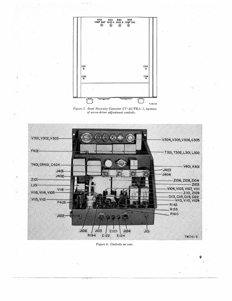
c. Chassis-Mounted Screw-Driver Controls. The following chart lists the screw-driver controls on the top of the converter chassis (fig. 5) and indicates their functions. (The channel A and B input and oscillator tuning capacitors listed are front panel controls in the C and D models (fig. 4).)
Controls
COMP AMP control (RI45).
BIAS A control (RI55)_
BIAS B control (RI60)_
COMP BAL control (R194)
Channel A input tuning capacitor (ClOl) (CHAN A INPUT).
Channel B input tuning capacitor (C103) (CHAN B I~PUT).
Channel A oscillator tuning capacitor (C105) (CHAN A OSC).
Channel B oscillator . tuning capacitor
(CI06) (CHAN B OSC).
8
!
Functions
Adjusts amount of feedback to the drift-compensating circuit.
Adjusts grid bias of the VlI3 driver amplifier tube so that polar output signals have equal positive and negative amplitudes.
Adjusts bias of the VlI4 d-c amplifier tube to give correct drift compensator input and to key tone oscillator.
. Adjusts plate voltage of the V1l4 d-c amplifier to balance mark and space voltage changes for equal swings in the drift compensator circuit. Works in conjunction with COMP AMP control.
Adjusts input frequency of channel A converter for maximum response to incoming i. f.
Adjusts input frequency of channel B converter for a maximum response to incoming i. f.
Adjusts oscillator section of channel A converter, to produce a second i. f. of 50 kc. Is a coarse tuning control that works in conjunction with the front panel CHANNEL A FINE TUNING control.
Adjusts oscillator section of channel B converter, to produce a second i. f. of 29.3 kc. Is a coarse tuning control that works in conjunction with the front panel CHANNEL B FINE TUNING control.
d. Chassis-Mounted Connectors. The following -connectors are located on the rear of the chassis (fig. 5):
Control
Channel A input jack J1Ol.
Channel B input jack JI02.
Signal output jack JI03.
A-c power input Jack J104.
Power connection jack J106. '
External receiver disabling jack J40l.
Receiver disabling jack J402.
Receiver disabling jack J403.
Control circuit input jack J404.
Plug P405 ______ . _____ _
Fuse F40L _________ _
Binding posts E122, E123, and E124.
Function
Connects channel A receiver i-f output to mixer VIOl input.
Connects channel B receiver i-f output to mixer V102 input.
Connects converter output (both neutral and polar) to external circuit.
Connects lI5-volt input power to power supply section.
Input for operating voltages from converter to the tone oscillator.
Breaks external receiver disabling line through relay K401 contacts.
Applies a positive voltage through pin B to the receiver disabling relay circuit.
Applies a p.ositive voltage through pin B to the receiver disabling relay circuit.
Input for disabling-relay operation and hand keying.
Connects tone oscillator to con" verter through jack JI06.
Fuses the tone oscillator section. Connected to pin B of J103,
ground, and pin D of JI03 to provide direct wire connections for polar and neutral loops,
e. Power Supply Fuses and Safety Switches. Fuses F301 and F302, which fuse the 115-volt, 50-cycles supply to Rectifier Power Unit PP-193 (*)/TRA-7 are behind the top panel door (fig. 4). F303 is a spare fuseholder, and is not wired into any circuits. Safety interlock switches S301 and S302 are so mounted in the upper panel door that the 115-volt, 50-cycle supply voltage is cut out automatically if the door is not securely fastened.
RI45 RI55 RI60 RI94 COMP AMP BIAS A BIAS B COUP BAL
® ® ® ®
CIOI CI03 e e
CI05 CI06 e e
0 """ ~ 0 TLSGII3S
Figure 5. Dual Diversity Converter CV-Sl/TRA-7, location of screw-driver adjustment controls. .
Figure 6. Controls on rear.
9
111111,111111 i
•
CHAPTER 2
ORGANIZATIONAL MAINTENANCE INSTRUCTIONS
Section I. PREVENTIVE MAINTENANCE SERVICES
9. Definition of Preventive Maintenance
Preventive maintenance is work performed on equipment (usually when the equipment is not in use) to keep it in such good working order that break-downs and needless interruptions in service will be kept to a minimum. Preventive maintenance differs from trouble shooting and repair, since its object is to prevent certain troubles from occurring.
10. Organizational Tools and Equipment
Tools and materials that should be available at the organizational level are listed in a and b below. The pertinent toolkit is listed in SIG 6-TE-113.
a. Tool Equipment. Tool Equipment TE-1l3. (Organizations
which have fixed plant Tool Equipments TE~87-(*) and TE-88-(*) available can dispense with Tool Equipment TE~113.)
b. Materials. Oranges tick. Cheesecloth, bleached, lint~free. Cloth, crocus, 9- by ll-inch sheets (spec
No. 42056-Navy). Carbon tetrachloride. Paper, sand, No. 000 and No. 0000 (Fed spec
No. P-P-111). Solvent, dry-cleaning (SD) (Fed spec No.
P-8-661s).
11. Genera"1 Preventive Maintenance Techniques
a. Use No. 0000 sandpaper to remove corrosion. b.Use a clean, dry, lint-free cloth or a dry
brush for cleaning.
10
(1) If necessary, except for electrical contacts, moisten the cloth or brush with solvent
(SD); then wipe the parts dry with a cloth.
(2) Clean electrical contacts with a cloth moistened with carbon tetr!).chloride; then wipe them dry with a cloth.
Caution: Repeated contact of carbon tetrachloride with the skin, or prolonged breathing of fumes is dangerous. Make sure adequdte ventilation is provided.
c. If available, dry compressed air may be used at a line pressure not exceeding 60 pounds per square inch to remove dust from inaccessible. places; be careful, however, or mechanical damage from the air blast may result.
d. For further information on preventive maintenance techniques, refer to TB SIG 178.
12. Use of. Forms in Performing Preventive Maintenance
(figs. 7 and 8)
a. The information in this paragraph is presented as a guide to the individual making an inspection of equipment in accordance with instructions on DA AGO Forms 11-238 and 11-239. The decision as to which items on the forms are applicable to this equipment is a tactical decision to be made, in the case of First Echelon Maintenance, by the Communication Officer/Chief or his designated representative, and in the case of Second and Third Echelon Maintenance, by the individual making the inspection. " Instructions for the use of each form appear on the reverse side of the form.
b. The first two columns of the chart in this paragraph- serve as a cross reference between the item numbers of DA AGO Forms 11-238 and 11-239 and the preventive maintenance information in this manual. Circled items on figures 7 and 8 are either partially or totally applicable to " Dual Diversity Converter CV-31 (*)jTRA-7.
OPERATOR FIRST ECHELON MAINTENANCE CHECK LIST FOR SIGNAL CORPS EQUIPMENT RADIO COHHUN I CATI ON, 01 RECTI ON FINDING, CARRIER, RADAR
INSTRUCTIONS: S~e other 3 ide
EQUIPMENT NOMENCLATURE EQUI P~ENT SER IAl NO •
LEGEND FOR MARKING CONDITIONS: .( Satisfactory; X Adjustment, repair or replacement required; ® Defect corrected. NOTE: Strike out i terns not applicable.
DA I LY
NO ITEM CONDITION
S M T • T F S
Q: COMPLETENESS AND GENERAL CONDITION OF EOU 1 PIro4ENT (receiver. t ransmj t t er. cBrryjn~ cases. "ire and cable, microphones, tubes, spate parts. ted-mica! manuals and accessories).
([ LOCATION AND INSTALLATION SUITABLE FOR NORMAL OPERATION.
,Cf CLEAN DIRT AND MOISTURE FROM AtHENNA, h41CROPHONE, HEADSET,S, CHEST SETS , KEYS, JACKS, PLUGS, TELEPHONES, CARRYING BAGS, CCNPONENT PANELS.
~-
~ INSPECT SEATING OF READ I Lv ACCESS ISLE "PLUCK-QUrlt ITEMS: TUBES, lAIo4PS, CRYSTALS, FUSES, CONNECTORS, V 18RATORS, PLUG-IN COilS AND RESISTORS.
--~
C2.. INSPECT CONTROLS FOR BINDING, SCRAPING, EXCESSIVE LOOSENESS, WORN OR CHIPPED GEARS, MISAlIGNIo!ENT, POS rnVE ACTION.
~ CHECK FOR NORt.4Al OPERAT I ON.
WEEKLY , , NO. ITEM ~~
::i>--
NO 'ITEM
~~ Q.
CLEAN AND TIGHTEN EXTERIOR OF COMPONENTS AND CASES, RACK 1)
MOUNTS, SHOCK 1040UNTS, ANTENNA MOUNTS, COAX' A L TRANS,", I SS I ON HISPECT STORAGE BATTER I ES FOR DIRT, LOOSE TERIo4!NALS, ELEC-
LINES, WAVE GUIDES, AND CABLE CONNECTIONS. TROLYTE LEVEL AND SPECIFIC GRAVITY, AND DAMAGED CASES.
:~ 14
INSPECT CASES, 1040UNTINGS, ANTENNAS, TOWERS, AND EXPOSED CLEAN AIR FILTERS, BRASS NA"f PLATES, DiAl AND METER METAL SURFACES, FOR RUST, CORROSION, AND t.40lSTURE. WINDOWS, J'EWEL A5SEt.4BLlES.
Ci 15 INSPECT CORD, CABLE, WIRE, AND SHOCK MOUNTS FOR CUTS, BRE~~;S, FRAYING, DETERIORATION, KINKS, AND STRAIN. INSPECT METERS FOR DA"AGED GLASS AND CASES.
-10 16
INS PECT ANTEtI'NA FOR ECCENTRICITIES, CORROSION, 'lOOSE FIT, INSPECT SHELTERS AND COVERS .FOR ADEQUACY OF WEATHER-DAIo!AGED INSUL:'ATORS AND REFLECTORS. PROOFING.
~ 17
INSPECT rANVAS ITEMS, LEATHE'R, AND CABLING FOR MI LDEW. TEARS, AND FRAYING. CHECK ANTENNA GUY WIRES FOR LOOSENESS AND PROPER TENS ION.
12 INSPECT FOR LOOSENESS OF ACCESSIBLE lTE"S: SWITCHES, 18 KNOBS, J AC KS, CONNECTORS, E LECTR ICA L TRANSFORMERS, POWER-
CHECK TER" INAl BOX COVERS FOR CRACKS, LEAKS, DAMAGED STATS, RELAYS, SELSYNS, 1040TORS, BLOWERS, CAPACITORS, GEN- GASKETS, D tRT AND GREASE. [RATORS, AND PILOT LIGHT ASSEMBLIES.
19 IF DEFICIENCIES NOTED ARE NOT CORRECTED DURING INSPECTION, INDICATE ACTION TAKEN FOR CORRECTION.
.
REPLACES DA AGO FOR" 419,1 OEC 50, WHICH IS OBSOLETE.
TM 261-44 Fig1lre 7. DA AGO Form 11-238.
11
II :1,111
'- -SECOND AND THIRD ECHELON MAINTENANCE CHECK LIST FOR SIGNAL CORPS fQUIPMENT
IADIO CO"MVIICATIOI. DIIECTIOI FIIDIlI. CAI,IEI. "ADAI
INSRIICTIONS: Se •• flt.,. .,d_ EQUIPMENT NQNENCLATURE EQUIPMENT SERIAL NO.
UGIND POI MARliNG CONDITIONS: ~ Satisfactory; I JdJa.atmeDt, repair or repl&cemea.t nllllired; . NOTK: Strike oat heme Dot au..,licable.
(!) Defect corrected.
il ,
NO ITEM o. ITEM 0
~
I\! COIIPL£TENESS AND GENERAL CONDITI()t.I OF EQUIPMENT (ree.i.." ·e ELECTRON TUBES - INSnCT fOR LOOSE ENVElOPES, CAP CONNEC-'ran_ift.r. cerr,'''' c ••••• _ir. end c""., .1eTophone., TORS, CRACKED SOCKETS: lNSUFFICIOIT SOCkET SPRING TENSION; , ...... • per. ,..r'., tecltrticel _anIM' •. erwl ace ••• ori •• ). CLEAN DUST AND DIRT CAREFULLY. CHECK EIIISSION Of RECEIVER
TYPE TUBES •
~ •• INSPECT FILM CUT-oUTS FOR LOOSE PARTS, DIRT, MISALIGNMENT LOCATION AND INSTALLATION SUITAB'.E fOR NORMAL OPEftATiON. AND CORROS ION.
IQ CLEAN DIRT AND III,)ISTURE FROM ANTENNA. MICROPHONE, HEADSETS, ~ INSPECT FI)(ED CAPACITOItS FOR LEAl'S, !lULGES~ AND OISCOLORA-CHESTSETS, KEYS, JACKS, PlUGS. TELEI"tIONES, CARRYING BAGS,
COMPONENT PAHELS. TION.
I\! INSPECT SEATING OF READILY ACCESSIBll "PLUCK-OUT" ITEMS: 22 INSPECT RELAY AND CIRCUIT BREAKER ASSEMBLIES FOR LOOSE
MOUNTlN6S; BURNEO. PITIEO. CORRODED CONHeTS; MiSALIGNMENT TUBES, LAMPS, CRYSTALS • .FUSES, CONNECTORS, VIBRATORS, OF CONTACTS AND SPRINGS; INSUFFICIENT SPRING TENSIOtl; BIND-PLUG-IN COilS AND RESISTORS. ING OF PLUNGERS AND HINGE PARTS.
I~ ., INSPECT CONTItOLS FOR BINDING, SCRAP1NG, EXCESSIVE LOOSENESS, INSPECT VARIABlE CAPACITORS FOR. DIRT, MOISTURE, MIUlIGN-
WORN M CHIPPED GEARS, MISALIGNMENT, POSITIVE ACTION. MENT Of PLATES, AND LOOSE MOUNTINGS •
6 .::. INSPECT RESISTORS, BUSHINGS. AND INSULATORS. FOR CRACKS. CHECK FOR NORMAL OPERAT ION. CHIPPING, BLISTERING, DISCOLORATION AND MOISTURE.
1 CLEAN AND TIGHTEN EXTERIOR OF COMPONENTS AND CASES, RACK ~ INSPECT TERMINALS OF LARGE FIXED CAPACITORS AND RESISTORS MOUNTS, SHOCK MOUNTS, ANTENNA MOUNTS, COUIAL TRANSMISSION
FOR CORROSION, DIRT AND LOOSE CONTACTS. LINES, WAVE GUIDES, AND CAtlLE CONNECTIONS.
I<! INSPECT CASES. MOUNTINGS, ANTENNAS, TOWERS, AND E)(POSED ~ CLEAN AND TIGIfTEN SIIIITCHES. TERMINAL BLOCKS. BLOWERS, METAL SURFACES, FOR RUST, CORROSION, AhlD MOISTURE. RElAY CASES. AND INTERIORS Of CHASSIS AND CABINEtS HOT
READILY ACCESSIBLE.
1\2 INSPECT CORD, CABLE, WIRE. AND SHOCK MOUNTS fOR CUTS, ~ INSPECT TERMINAL BLOCKS FOR LOOSE CONMECTIONS, CRACKS BREAKS, FRAYING, DETERIORATION, KINKS, AND STRAIN. AND BREAKS.
I. 2. INSPECT ANTENNA FOR [CCENTRICITIES. CORROSION, LOOSE FIT. DAMAGED INSULATORS AND REFLECTCRS. CHECK SmlNGS OF Al),JUSTA8LE RELAYS.
t-'= 29 INSPECT CANVAS ITEMS. LEATHER, AND CABLING FOR NI LOE', LUBRICATE EQUIPMENT IN ACCCRDANCE WITH APPLICABLE TEA~. AND fRAYING. DEPARTMENT GF THE ARMY LU8RICATIOH ORDER.
12 INSPECT FOR LOOSENESS Of ACCESSIBLE ITO.S: SWITCHES, KNOBS, ). ""CKS, CONNECTORS, ELECTRICAL TRANSFORME'IS, POWERSTATS, INSPECT GENERATORS, AMPLI/)YNES. DYNAMOTORS. FOR BRUSH IUR, RELAYS t SELSYNS, MOTORS, 8LOWERS, CAPACITORS, GENERATORS, SPRING TENSION. ARCING, AND FITTING OF COMMUTATOR. AND PILOT LIGHT ASSEM8LIES.
I) ~ INSPECT STORAGE SATTERIES FOR DIRT, LOOSE TERMINA.LS; CLEAN AND TIGHTEN CONNECTIONS AND MOUNTINGS FOR TRANSFORMERS ELECTROLYTE LEVEL AND SPECIFIC GRAVITY, AND DAMAGED CASES. CHOKES, POTENTIOMETERS, AND RHEOSTATS.
" ~ CLEAN AIR FILTERS, 8RASS NANE PLATES, DIAL AHO METER INSPECT TRANSfORMERS, CHOKES. POTENTIOMETERS. AND WINDOWS. dEWEl ASSEMBLIES .• RHEOSTATS 'FOR OVERHEATING AND OIL-LEAKAGE.
1, " INSPECT METERS FOR OAI£AGED GLASS AND CAUS. IEFORE StlIP"NG OR STORING" REMOVE BATTERIES.
16 ,. INSPECT SHELTERS AND COVERS fOR ADEOIIACY OF WEATHE"PROOFIN6. INSPECT CATHODE RAY TUBES FOR flURNT SCREEN SPOTS.
11 " CHECK ANTENNA GUY WIRES FOR LOOSENESS A.ND PROPER TENSION. INSPECT SAnER IES FOR StiOATS AND DEAD CELLS..
18 )6 INSPECT fOR LEAKING WATERPROOF GASKETS, WORN DR LOOSE PARTS. CHECK TERMINAL BOX COYERS FOR CRACKS, LEAKS, DAMAGEO
GASKETS, DIRT AND GREASE.
~ MOISTURE AND FUNGI PROOf. ,. IF DEFICIENCIES NarED ARE NOT CORRECTED DURING INSPECTION, IROICATE ACTION TAKEN FOR CORRECTION.
\ \
DA ~-:.~~11-239 REPLACII DA "80 P'OW. 1119, 1 DEt ,0, IHICH IS 08S0LETE.
TM 261-45
12 Figure 8. DA AGO Form 11-239.
c. The following preventive maintenance opera
tions should be performed at the intervals indicated, unless these intervals are reduced by the local commander.
Caution: Screws, bolts, and nuts should not be tightened carelessly. Fittings tightened beyond the pressure for which they are designed will be damaged or broken.
DA AGO DA AGO Form Form 11-238 11-239 Procedure
Item No. Item No.
1
2
3
4
5
6
7
8
DAILY
1 Check for completeness and satisfactory condition of the control unit.
2 Check suitability of location and installation for normal operation.
3 Remove dirt and moisture from cords, jacks, plugs, and panels of the component parts.
4 Inspect the seating of the fuses (figs. 4 and 6) and all plugs and connectors.
5 Inspect all controls for binding, scraping, excessive looseness, worn shafts, misa:linement, and positive action.
6 Check for normal operation.
WEEKLY
Caution: Disconnect all power before performing the following operations. Upon completion, reconnect power and check for satisfactory operation.
7 Clean and tighten the panel mountings.
8 Inspect case, mounting, and exposed metal surfaces for rust, corrosion, and moisture.
DA AGO DA AGO Form Form Procedure 11-238 11-239
Item No. Item No.
9
11
WEEKLY-Continued
9 Inspect cords, cables, wires, and shock mounts for cuts, breaks, fraying, deterioration, kinks, and strain.
11 Inspect TM 11-261 for tears, mildew, or fraying.
MONTHLY
19 Inspect electron tubes for loose envelopes, loose cap connectors, cracked sockets, and insufficient socket spring tension; check emission of tubes.
Note. Tubes with suffix letters Y or W may be substituted for their prototypes; i. e., 6SJ7Y may be used for a 6SJ7. .
21 Inspect fixed capacitors for leaks, bulges, and discoloration.
24 Inspect resistors, bushings, and insulators for cracks, chippings, blistering, discoloration, and moisture.
25 Inspect terminals of large fixed capacitors and resistors for corrosion, dirt, and loose contacts.
26 Clean and tighten switches, terminal blocks, relay, and interior of chassis.
27 Inspect terminal blocks for loose connections, cracks, and breaks.
31 Clean and tighten connections and mountings for transformers, potentiometers, and rheostats.
32 Inspect transformers, potentiometers, and rheostats for overheating and oil leakage.
37 Check adequacy of moisture and fungiproof treatment.
28 If deficiencies noted are not corrected during inspection, indicate what action was taken to correct the deficiencies.
Section II. LUBRICATION· AND WEATHERPROOFING
13. Lubrication The lubrication of the converter is relatively
simple. Clean the shafts and areas adjacent to the switch shaft bearings. Apply one or two drops of special preservative (PI .. ) lubricating oil to the bearings .. Wipe off excess oil.
14. Weatherproofing a. General. Signal Corps equipment, when op
erated under severe climatic conditions such as
I i I
prevail in tropical, arctic, and desert regions, requires special treatment and maintenance. Fungus growth, insects, dust, corrosion, salt spray, excessive moisture, and extreme temperatures are harmful to most materials.
b. Tropical Maintenance. A special moistureproofing and fungi-proofing treatment has been devised which, if properly applied, prOVIdes a reasonable degree of protection. This treatment is explained in TB SIG 13 and TB SIG 72.
c. Winter Maintenance. Special precautions
13
necessary to prevent poor performance or total operational failure of equipment in extremely low temperatures are explained in TB SrG 66 and TB SrG 219.
d. Desert Maintenance. Special precautions necessary to prevent equipment failure in areas subject to extremely high temperatures, low humidity, and excessive sand and dust are exexplained in TB SrG 75.
e. Lubrication. The effects of extreme cold and heat on lubricating materials and lubricants are explained in TB SIG 69. Observe all precautions. outlined in TB SIG 69 and pay strict attention to all lubrication orders when! operating equipment under conditions of extreme cold or heat.
15. RustprooFing and Painting
a. When the finish on the case has been badly
14'
scarred or damaged, rust and corrosion can be prevented by touching up bared surfaces. Use No. 00 or No. 000 sandpaper to clean the surface down to the bare metal. Obtain a bright smooth finish.
Caution: Do not use steel wool. Minute particles frequently enter the case and cause harmful internal shorting or grounding of circuits.
b. When a touch-up job is necessary, apply paint with a small brush. When numerous scars and scratches warrant complete repainting, remove the panels and chassis, and spray paint over the entire case. Remove rust from the case by cleaning corroded metal with solvent (SD). In severe cases it may be necessary to use solvent (SD) to soften the rust and to use sandpaper to complete the preparation for painting. Paint used will be authorized and consistent with existing regulations. Refer to TM 9-2851.
CHAPTER 3
THEORY
Section I. SYSTEM THEORY
16. Scope Dual Diversity Oonverter OV-31(*)JTRA-7 is
used with a combination of radio and wire equipments working as a unit and involving practices and theory of both. For this reason, a few of the basic principles of teletypewriter theorywiil be discussed in this section. For detailed data on the theory of teletypewriter components, refer to TM 11-680. The functions of the converter unit in a representative RR T system is covered in paragraph 24.
17. Signaling Currents Radioteletype systems use teletypewriters (tele
graph printers) that will operate normally over 10 to 20 miles of unloaded (no extra inductances added) field Wire W-llO-B 'without repeaters or
IDEAL
MARK 60 MA D [1. o MA
SPACE
NEUTRAL
MARK + 25 MA
OMA--~~~----~----~-
-25 MA SPACE
POLAR
line relays. The distance depends on whether battery (current) is supplied at one or both' ends of the line.
a. Methods. Two methods of transmitting TT signals on wire lines are normally used-the neutral system and the polar system. In the neutral system, use is made of current on and current oj! square-wave pulses of one polarity. The polar system uses positive and negative square-wave pulses. Figure 9 shows ideal and practical signal pulses. The transitions from one signal condition to the other and the timing of the transitions, determine the intelligence conveyed.
b. Neutral System. In the neutral system, current is sent over the line to operate the receiving TT selector mechanisms to a marking position, aad the current is stopped to operate the selecting magnets toa spacing position. A marking current
PRACTICAL
C\Q
T M 264-47
Figure 9. Neutral and polar waveshapes ..
15
II 1,:,1 I
of 60 ma normally is used. Neutral operation is used in the monitor loop circuit of this unit (con~ nections are made through D and E of J103). .
c. Polar System. In the polar system, current is sent over the wire in one direction for the marking impulses and in the opposite direction for the spacing impulses. Polar operation possesses a number of advantages <;lvcr the neutral sy::;tem and is used in the extension circuits (A and B, JI03) of this unit. Two of the major advantages are-
(1) Apparent voltage gain. The transmission of current in the opposite direction for spacing gives the effect of increased voltage without increasing the current values in any part of the circuit. Therefore, the· circuit is not subjected to as high working voltages as in the neutral system.
(2) Decreased bias. The presence of bias (lengthening or shortening of the signal wave) on the line has little effect on the resulting waveform of the signal transmitted with pola,r operation. If the mark and space currents have been adjusted correctly at the sending end of the circuit, the electrostatic charges remaining in the transmission line from the positive and negative impulses cancel, leaving the waveform undisturbed.
d. Use. Neutral operation is used satisfactorily for short lines; it is used also to operate the selector magnets of the TT equipments. Polar operation is invariably used where long lines or highly-capacitive circuits are involved.
18. Teletypewriter Code
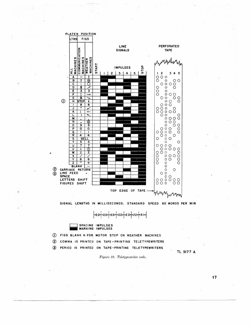
a. Assuming that two typewriters are to be connected together by a wire or wires so that messages typed on one would be automatically and simultancously typed on the other, the first method of accomplishment might be to have each key of the sending typewriter connected by an individual wire to a magnet for a corresponding type bar of the receiving typewriter. Such an arrangement would be:very simple in thcory, but obviouslyuneconomical in the amount of material used. An economical method of solving the problem is by sending a sequence of signals, or code, for each character as is done in the case of manual Morse telegraphy. This is the general method used with teletypewriters although the code is considerably altered to adapt it for best machine operation.
16
! b. In selecting a satisfactory code for TT operation, several factors had to be considered, including the following: , (1) The code should preferably use only two
line conditions, such as current and no current.
(2) The number of code elements per character should be a minimum in order to permit high-speed operation Over relatively narrow-band telegraph circuits. (A greater' keying speed is equivalent to more information per unit time; the more information transmitted in a given time, the greater the necessary bandwidth.)
(3) The number of code units per character should preferably be uniform in order to give simple machine design.
c. A code answering the general requirements is the one used in our present teletypewriters; it is usually called the five-unit selecting code. There are 32 possible ways of arranging two current values with respect to five divisions of time, making possible the selection of anyone of 32 type bars or other operating mechanisms. By using each type bar for two characters, this code is sufficient to provide for the 26 letters of the alphabet, the ten numerals, and the usual punctuation marks. It is the shortest practical code for two-line conditions.
d. The mark and space impulses used to operate a teletypewriter are pulses of direct current of uniform intensity (figs. 9 and 10). If oscilloscope test prods were connected across a line carrying these mark and space impulses, they would appear as a square waveform (fig. 9). It is very important that the transmitted impulse maintain its waveform when it reaches the receiving apparatus, since a steady impulse is necessary for correct operation of the receiving machine. When sending at 60 wpm (words per minute), assuming a standllrdfive-Ietter word, the time for each unit signal impulse is 22 ms (milliseconds) (fig. 10). When the selecting mechanism of the receiving teletypewriter is adjusted correctly, it operates only during the central portion of the received signal impulse, requiring only 20 percent of the unit interval, or approximately 4 ms. It is apparent from the above that there are many factors that may cause false operation of the receiving teletypewriter. Improper adjustment of receiving and sending equipment may' result in improper synchronization and consequent false operation. Link (connecting wire) leakage, line
PLATEN POSITION
CD
B ® CARRIAGE @ LINE FEED
SPACE
FIGS
LETTERS SHIFT FIGURES SHIFT
LINE SIGNALS
TOP EDGE OF TAPE
PERFORATED TAPE
I 2 3 4 5 000 o 0 00
0000 000 o 0 o 000
00 00 00 0
000 000 0 00000
00 0 0000 000 o 00
000 0 0000 0
00 0 o 00
o 0 0000
00000 000 0 o 0000 o 00 0 000
o o 0
00 00
000000 000 00
SIGNAL LENGTHS IN MILLISECONDS. STANDARD SPEED 60 WORDS PER MIN
.. SPACING IMPULSES MARKING IMPULSES
CD FIGS BLANK H FOR MOTOR STOP ON WEATHER MACHINES
® COMMA IS PRINTED ON TAPE-PRINTING TELETYPEWRITERS
@ PERIOD IS PRINTED ON TAPE - PRINTING TELETYPEWRITERS
TL 9177 A Figure 10. Teletypewriter code.
I I I
17
---~--~---
resistance, ground resistance, ground potentials (caused by earth eurrents), and-changes in electrical constants in the involved components may all create waveshape distortion.
19. Transmitter-distributor
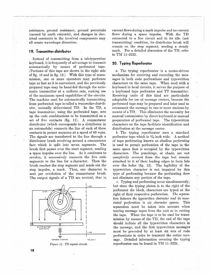
Instead of transmitting from a teletypewriter keyboard, it is frequently of advantage to transmit automatically by means of perforated tape. (Portions of this tape are shown in the right side of fig. 10 and in. fig. 12.) With this type of transmission, one or more operators may perforate tape as fast as it is convenient, and the previously prepared tape may be hand-fed through the automatic transmitter at a uniform rate, making use of the maximum speed capabilities of the circuits. The machine used for automatically transmitting from perforated tape is called a transmitter-distributor, normally abbreviated TD. In the TD, a tape transmitter, using the perforated tape, sets up the code combinations to be transmitted on' a set of five contacts (fig. 11). A commutator distributor (which corresponds to a distributor in l:tll automobile) connects the line of each of these contacts in proper sequence at a speed of 60 wpm. The signals are transferred to the line through a distributor brush revolving around a commutator face which is split into seven segments. The brush first passes over the start segment, sending a space impulse over the line. As it continues to revolve, it successively connects the five code segments to the line for a character. Then the brush reaches the stop segment and sends out the stop impulse, a mark. Thus, one character is sent per revolution of the commutator brush. The output signals of a TD are neutral; that is,
18
DISTRIBUTOR CONTACTS
J SENDING STATION
. Figure 11. TD signal. circu.it.
LINE
LINE
current flows during a mark impulse and no current flows during a space impulse. With the TD connected to a line circuit and in its idle (not transmitting) condition, its distributor brush will remain on the stop segment, sending a steady mark. For a detailed discussion of the TD, refer to TM 11-2222.
20. Typing ReperForator
a. The typing reperforator is a motor-driven mechanism for receiving and recording the messages in both code perforations and typewritten -characters on the same tape. When used with a keyboard in local circuits, it serves the purpose of a keyboard tape perforator and TT transmitter. Receiving units of this kind are particularly adaptable for use at message centers, because the perforated tape may be prepared and later used to retransmit the message to one or more stations by means of a TD. This eliminates the necessity for. manual transmission by direct keyboard or manual preparation of perforated tape. The typewritten characters on the tape facilitate identification and distribution at the message center.
b. The typing reperforator uses a standard perforator tape which is lX'6 inch wide. A method of tape perforating known as chadless perforating is used to permit perforation of the tape in the same space that is occupied 1)y the typewritten characters. The punchings, or chads, are not completely severed from the tape but remain attached to it at· their leading edges to form lids over the holes (fig. 12). The legibility of the typewritten character is not impaired by this type of perforating because the perforating does not eliminate any portion of the tape.
c. Typing and perforating occur simultaneously, but since the typing platen is to the right of the perforator die block, characters are typed at the right of their respective perforation. The separation between the typewritten character and its associated perforation is six character spaces. This separation must be taken into account when tearing message tapes from the unit @r in cutting the tape. When the tape is to be used for transmission by means of the TD, the end of the tape should include all the typewritten characters in the message, and the first typewritten messages must be preceded by at least six sets of code perforations in order to transmit the entire message. Detailed information covering the typing reperforatorcan be found inTM 11-2223 .
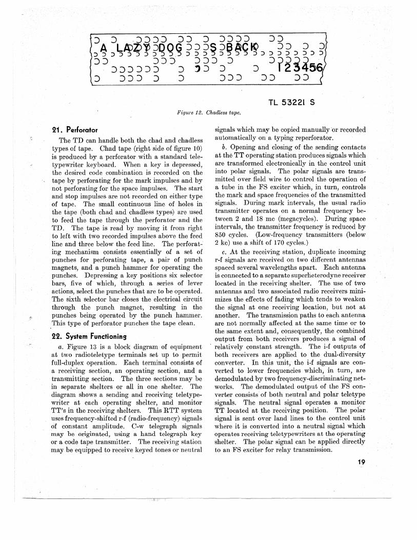
TL 53221 S Figure 12. Chadless tape.
21. Perforator
The TD can handle both the chad and chadless types of tape. Chad tape (right side of figure 10) is produced by a perforator with a standard teletypewriter keyboard. When a key is depressed, the desired code combination is recorded on the tape by perforating for the mark impulses and by not perforating for the space impulses. The start and stop impulses are not recorded on either type of tape. The small continuous line of holes in the tape (both chad and chadless types) are used to feed the tape through the perforator and the TD. The tape is read by moying it from right to left with two recorded impulses above the feed line and three below the feed line. The perforating mechanism consists essentially of a set of punches for perforating tape, a pair of punch magnets, and a punch hammer for operating the punches. Depressing a key positions six selector bars, five of which, through a series of lever actions, select the punches that are to be operated. The sixth selector bar closes the electrical circuit through the punch magnet, resulting in the punches being operated by the punch hammer. This type of perforator punches the tape clean.
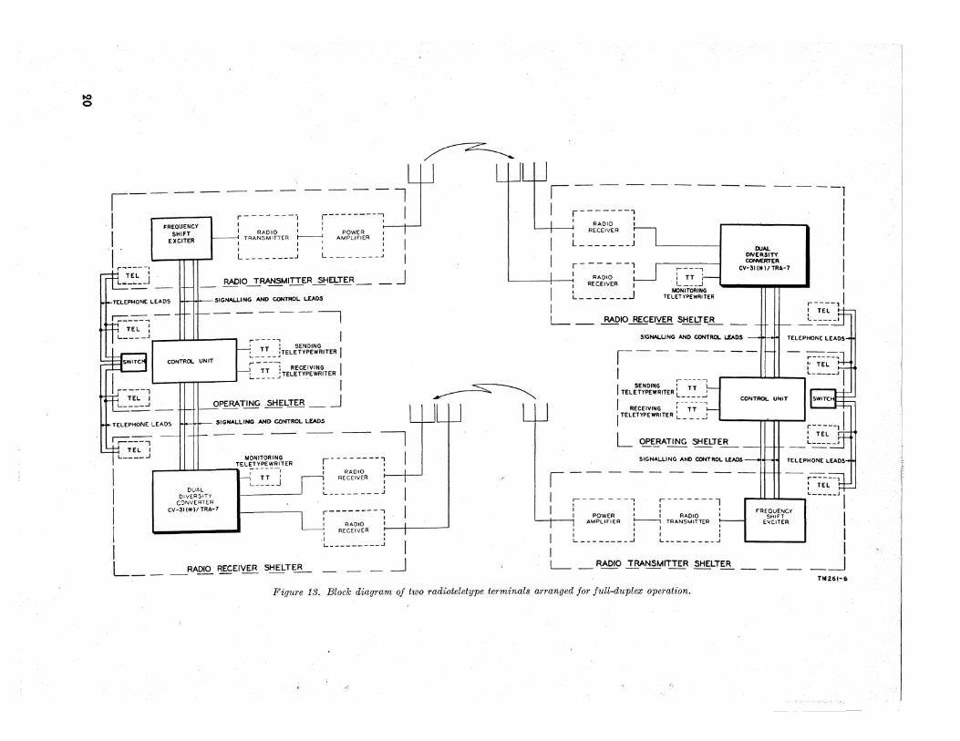
22. System Functioning
a. Figure 13 is a block diagram of equipment at two radioteletype terminals set up to permit full-duplex operation. Each terminal consists of a receiving section, an operating section, and a transmitting section. The three sections may be in separate shelters or all in one shelter. The diagram shows a sending and receiving teletypewriter at each operating shelter, and monitor TT's in the receiving shelters. This RTT system uses frequency-shifted r-f (radio-frequency) signals of constant amplitude. C-w telegraph signals may be· originated, using a hand telegraph key or a code tape transmitter. The receiving station may be equipped to receive keyed tones or neutral
I Pil
signals which may be copied manually or recorded automatically on a typing reperforator. .
b. Opening and closing of the sending contacts at the TT operating station produces signals which are transformed electronically in tho control unit into polar signals. The polar signals are transmitted over field wire to control the operation of a tube in the FS exciter which, in turn, controls the mark and space frequencies of the transmitted signals. During mark intervals, the usual radio transmitter operates on a normal frequency between 2 and 18 me (megacycles). During space intervals, the transmitter frequency is reduced by 850 cycles. (Low-frequency transmitters (below 2 kc) use a shift of 170 cycles.)
c. At the receiving station, duplicate incoming r-f signals are received on two different antennas spaced several wavelengths apart. Each antenna is connected to a separate superheterodyne receiver located in the receiving shelter. The use of two antennas and two associated radio receivers minimizes the effects of fading which tends .to weaken the signal at one receiving location, but not at another. The transmission paths to each antenna are not normally affected at the same time or to the same extent and, consequently, the combined output from both receivers produces a signal of
. relatively constant strength. The i-f outputs of both receivers are applied to the dual-diversity converter. In this unit, the i-f signals are converted to lower frequencies which, in turn, are demodulated by two frequency-discriminating networks. The demodulated output of the FS converter consists of both neutral and polar teletype signals. The neutral signal operates a monitor TT located at the receiving position. The pofar signal is sent over land lines to the control unit where it is converted into a neutral signal which operates receiving teletypewriters at the operating shelter. The polar signal can be applied directly to an FS exciter for relay transmission.
19
10 o
1------- j~ I ---l I r---- I FREQUENCY , ----, ,----------,
SHIFT I RADIO ~: I I EXCITER TRANSM ITTER ~ POWER I
, I I I . I I I AMPLIFIER
r~----' L ________ ~ L ________ ~
, ,
M'-RADIO~RANSMITTER ~ELTER_
LEADS .J--- S'GNALLI NG AND CONTROL LEAOS
+------ I ,- - --, , : SENDING :.... _ ~T __ ~TELETYPEWRITER I r-----.
: RECEIVING :.... _ ~~_ ~ TELETY~EWRITER I
CONTROL UN IT
I I
J
tc I r------~: I RAOIO r
RECEIVER 1
I _ J
I I
L _____ _
r------, , RADIO
I RECEiVER I
L _______ J
L- _ RADIO RECEIVER SHELTEB-
--1
I I I
CUAL I DIVERSITY CONVERTER I
CV-31 (*)ITRA-7
-- - t-
I r-...:--,I , TEL , c.
SIGNALU NG ANO CONTROL LEADS ----0 TELEPH ,------I .-- -----, i
r
" I c !! II
JB 1 I
I ~ ~
SENDING : TT }--I TELETYPEWRITER L ____ ~ I CONTROL UN'T
I RECEIVING : --T-T--~ I~
I I I I I L_
~PERATING SHELTER
LEADS
--t---- SIGNA.LLING AND CONTROL LEADS
+--- --- --- I I MONITORING
J! !! TEL~T!~~~~TER
H TT :
DUAL DIVERSITY
C')NVERTER CV-31 (*)1 TRA-7
L ____ J
_RADIO RECEIVER SHELT~
,- --- ----, , I
I RADIO I 1 RECEiVER f-I _-+_..J , , , I L ________ J
r--------..., , RADIO I
I REGEl VER :>--+------' ,I , L _________ J
I ~
I TELETYPEWRITER L - - .;.. --.J L' ----"1 i.....,I~Ir--.... :
L L OPERATING SHELT~ ----j r-SIGNALLING AND CONTROL LEADS--44- T[L[PH ,--------- ~
I ~ ___ '__J I ,--------, r-------l I "
I : POWER : : RADIO: rR[S~~~~GY I I I AMPLIFlER!-----1, TRANSMITTER ExCITER
, 1
I I I I I I t I I L ________ --' L ________ ..J I
'-- _ RADIO TRANSMITTER SHELTER -~ TM261-&
Figure 13_ Block diagram of two rad1;oteletype terminals arranged for full-duplex operation_
Section II. THEORY OF DUAL DIVERSITY CONVERTER
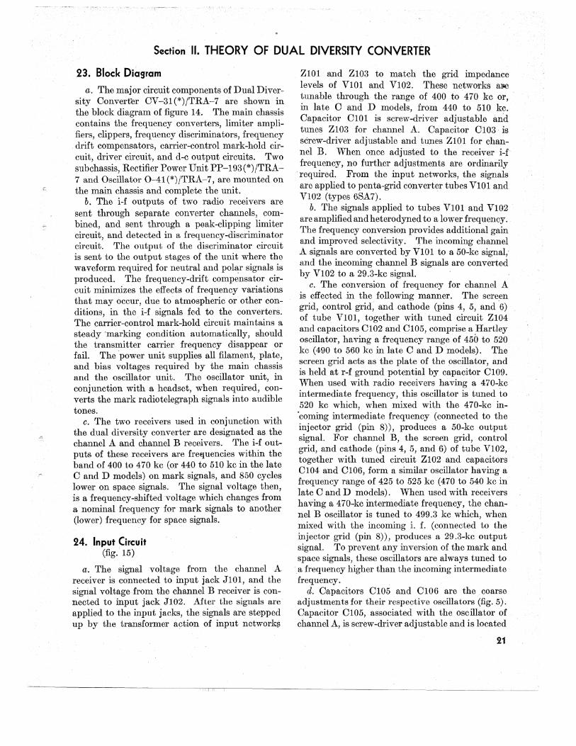
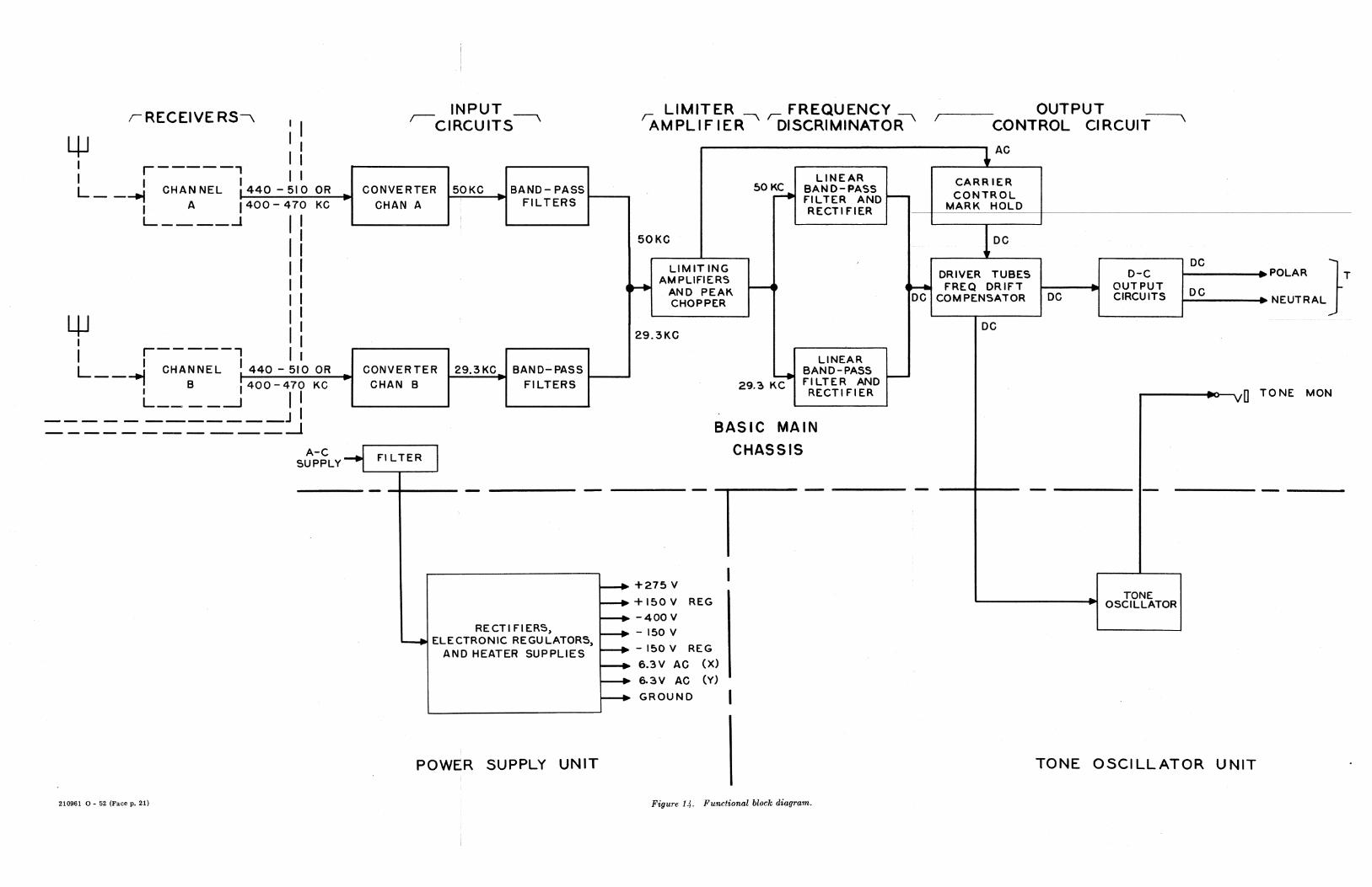
23. Block Diagram a. The major circuit components of Dual Diver
sity Converter OV-31(*)jTRA-7 are shown in the block diagram of figure 14. The main chassis conta~s the frequency converters, limiter amplifie-:s, chppers, frequency discriminators, frequency
. drift compensators, carrier-control mark-hold circuit, driver circuit, and d-c output circuits. Two sub chassis, Rectifier Power Unit PP-193 (*) jTRA-7 and Oscillator 0-41 (*)/TRA-7, are mounted on the main chassis and complete the unit.
b. The i-f outputs of two radio receivers are sent through separate converter channels combined, and sent through a peak-clipping limiter circuit, and detected in a frequency-discriminator circuit. The output of the discriminator circuit is sent to the output stages of the unit where the waveform required for neutral andpolar signals is produced. The frequency-drift comp~nsator circuit minimizes the effects of frequency variations that may occur, due to atmospheric or other conditions, in the. i-f signals fed to the converters. The carrier-control mark-hold circuit maintains a steady 'marking condition automatically, should th.e transmitter carrier frequency disappear or fail. ?,he power unit supplies all filament, plate, and blaS voltages required by the main chassis and the oscillator unit. The oscillator unit ~ . . . ' conjUnctIOn wIth a headset, when required, con-verts the mark radiotelegraph signals into audible tones.
c. The two receivers used in conjunction with the dual diversity converter are designated as the channel A and channel B receivers. The i-f outputs of these receivers are frettuencies within the band of 400 to 470 kc (or 440 to 510 kc in the late C and D models) on mark signals, and 850 cycles ~ower on space signals. The signal voltage then, IS a frequency-shifted voltage which changes from a nominal frequency for mark signals to another (lower) frequency for space signals.
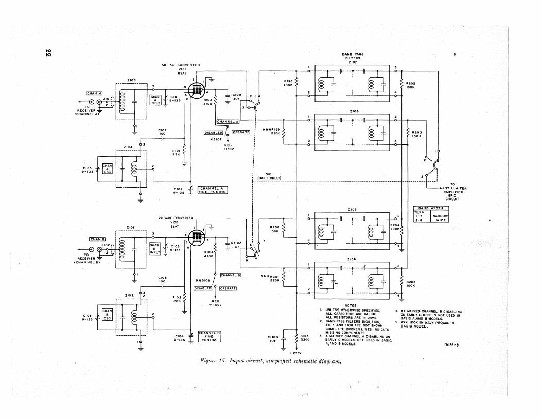
24. Input Circuit (fig.: 15)
a. The signal voltage from the channel A receiver is connected to input jack J101 and the sigxj.al voltage from the channel B receiv~r is connected to input jack J102. After the signals are· applied to the input jacks, the signals are stepped up by the transformer action of input network~
1",1 ii, I
ZlOl and Zl03 to match the grid impedance levels of VIOl and V102. These networks aBe tunable through the range of 400 to 470 kc or in lat~ C and D models, from 440 to 51Okc: CapaCItor ClOl is screw-driver adjustable and tunes Z103 for channel A. Capacitor Cl03· is screw-driver adjustable and tunes ZlOl for channel B. When once adjusted to the receiver i-I freq~ency, no further adjustments are ordinarily
. reqUITed: From the ~put networks, the signals are applIed to penta-grId converter tubes VIOl and V102 (types 6SA7). .
b. The signals applied to tubes VIOl and Vl02 are amplified and heterodyned to a lower frequency. The ~requency conversion provides additional gain and Improved selectivity. The incoming channel A signal~ are C?nverted by VIOl to a 50-kc signal,' and the mcommg channel B signals are converted by VI02 to a 29.3-kc signal. 0 0
c. The conversion of frequency for channel A is effected in the following manner. The screen grid, control grid; and cathode (pins 4, 5, and ·6) of tube VlOl, together with· tuned circuit Z104 and capacitors C102 and 0105, comprise a Hartley oscillator, having a frequency range of 450 to 520 kc (490 to 560 kc in late C and Dmodels). The screen grid acts as the plate of the oscillator and is held at r-f ground potential by c~pacitor C109. When used with radio receivers having a 470-kc intermediate frequency, this oscillator is tuned to 520 kc which, when mixed with the 470-kc in'coming intermediate frequency (connected to the i~jector grid (pin 8», produces a 50-kc output sI~al. For channel B, the screen grid, control grId, and cathode (pins 4, 5, and 6) of tube Vl02, together with tuned circuit Z102 and capacitors 0104 and 0106, form a similar oscillator having a frequency range of 425 to 525 kc (470 t9. 540 kc in late C and D models). When used with receivers having a 470-kc intermediate frequency, the channel B oscillator is tuned to 499.3 kc which, when mixed with the incoming i. f. (connected to the ~jector grid (pin 8», produces a 29.3-kc output SIgnal. To prevent any inversion of the mark and space signals, these oscillators are always tuned to
°a frequency higher than the incoming intermediate frequency.
d. Capacitors 0105 and Cl06 are the coarse adjust~ents for their respective oscillators (fig. 5). OapaCItor C105, associated with the oscillator of channel A, is screw-driver adjustable and is located
21
,RECEIVERS,
4J I r-----'
I I I I I 1
I I L CHANNEL --....j
I I ~ 440 - 510 OR
I A L ____ ...l
1400 - 470 KC
I I I I I I 1 I 1 1
I I I I I :
I 440 - 510 OR
,400-470 KC
I I __ J I -~
LW I I r-----'
I L_---i CHANNEL
I B L ____ -1
A-C SUPPLY
210961 0 - 52 (Face p. 21)
r
INPUT r-CIRCUITS ~
LIMITER FREQUENCY 'AMPLIFIER---- 'DISCRIMINATOR'
LINEAR CONVERTER 50KC BAND- PASS 50K~ BAND-PASS -
CHAN A r
FIL TERS fiLTER AND RECTI flER
) i
50KC
LIMITING
...... AMPLIfiERS f---4' ....... AND PEAK DC CHOPPER
29.3KC
LINEAR CONVERTER 29.3KC BAND-PASS
29.3 K~ BAND-PASS -CHAN B FILTERS F"lLTER AND RECTI FIER
BASIC MAIN
FI L TER I CHASSIS
- - - - - -
RECTIFIERS, ~ ELECTRONIC REGULATORS,
AND HEATER SUPPLIES
POWER SUPPLY UNIT
~+275V
f--+ + 150 V REG
r---+ -400 V f--+ - 150 V
f--+ - 150 V REG
--+ 6.3V AC (X)
6.3V AC (y)
GROUND
I
Figure 14. Functional block diagram.
/ OUTPUT
CONTROL CIRCUIT
~ AC
CARRIER CONTROL
MARK HOLD
DC
DRIVER TUBES D-C fREQ DRifT OUTPUT
COMPENSATOR DC CIRCUITS
DC
- -
.. TONE OSCILLATOR
\
DC POLAR }T DC
NEUTRAL
D TONE MON
-
TONE OSCILLATOR UNIT
N) N)
ZIO']
~~ TO
RECEIVER (CHANNEL Af
CI05 9-135
~ TO
RECEIVER <CHAN NEL. B)
CI06 9-13'5
~ ~
ICH:"! asc
Zl04
ZIOI
I L ________
50- KC CONVERTER VIOl
el07 100
eSA7
RIOI 22K
CIOO ! 2 I .fur
RI98 lOOK
2
, , , r.g~H~A~N~N~E~L-A~IL-----i----------~---}----o I
JDISABLf:D! ~ IOPERATE!
*5107 1 REG
+ISOV
, ! ***;~~= : : : I
i :
BANO PASS FILTERS
ZI07
ZIO&
4
4
R202 lOOK
R203 lOOK
2
: 5101 ~_l~~~~_~~':~~L _____ J ________________________________________________ LL ____ ~_
TO I ST LIMITER AMPLIFIER
GRID CIRCUIT
&SA7
i C"aAN f CI03 I INPUT 9-135 I "':'"
____ J cloe 100
RI02 '$ 22K
~ .....L.CIIO ..
T .IUF
R 104 4700
**5108
} !~"',,! !DISASLED! r !OPERAfE!
I REG + ISOV
! , , , i , , !
i , 8\
\
R200 lOOK
** *" R201 220K
eliOB
.oUF 1 Rlas 2200
+275V
2105
ZI06
NOTES
I. UNLESS OTHERWISE SPECIFIED, ALL CAPACITORS ARE IN UUF. ALL RESISTORS ARE IN OHMS.
2. BAND-PASS FILTERS llD5,llD6, i!: 107, AND ~ 108 ARE NOT SHOWN COMPLETE. BROKEN LINES INDiCATE MISSING COMPONENTS.
3. * MARKED CHANNEL A DISABLING ON EARLY C MODELS. NOT USED IN 9ASIC . A, AND B MODELS.
Figure 15 .. Input circuit, simplified schematic diagram.
4
4
R20S lOOK
BAND WIDTH
4. ** MARKEl;) CHANNEL 80lSABLING ON EARLY C MODELS. NOT USED IN BASIC, A.AND B MODELS.
5 MJUE lOOK IN NAVY PRO:CUREO 8~SIC ,",OOEL.
rM 26,1-$
adjacent to capaCitor 0101. Capacitor 0106, associated with the oscillator of channelB, is also screw-driver adjustable and is located adjacent to capacitor 0103. The OHANNEL A FINE TUNING and OHANNEL B FINE TUNING controls are capacitors 0102 and 0104 respectively. These are controlled by knobs on the front panel of the converter (fig. 3) . The range of adjustment of these controls in the b&sic through B models is as follows:
Range of adjustment in cycles Oscillator frequency
Channel A (C102) ChannelB (0104)
395 kc ____ ~_ 1,560_ _ _ _ _______ _ _ __ _ _ _ _ _ __ 920 470 kc ______ More than 2,000____________ 1,460 475 kc ______ More than 2,000____________ 1,660
e. To reject certain noise frequencies and interference from nearby transmitting stations, the bandwidth should be limited to a value not to exceed that which is adequate for the particular signals received. Accordingly, by turning BAND WIDTH switch 8101 to NARROW or WIDE, the outputs of mixer tubes V101 and Vl02 are connected to either a narrow-band or a wide-band filter. The association of the switch positions, the channels, the filters, and the frequency bandwidths are as follows:
Channel SI01 switch position Filter Frequency range
A _____ NARROW _____ ZI07 __ 50 kc±750 cps. A _____ WIDE, ________ c Z108 __ 50 kc ± 1500 cps. B _____ NARROW _____ ZI05 __ 29.3 kc±750 cps. B _____ WIDE _________ Z106 __ 29.3 kc± 1500 cps.
j. Ohannel A and channel Bare 'separate and distinct through the band-pass filters and up to the grid circuit of first limiter amplifier tube VI03 (type 68J7). The two frequencies of channels A and B are combined across the grid resistor (of VI03), which is comprised of resistor R203 in series with R205 (WIDE bandwidth) or resistor R202 in series with R204 (NARROW bandwidth).
25. Limiter Amplifier (fig. 16)
a. Frequency-shifted telegraph signals, radiated from the transmitting antennas, vary in frequency in accordance with the original d-c marking and
i, II I
spacing telegraph signals, but are virtually constant and amplitude. In the radio link between the transmitter and the receiver, thef;"!e signals may encounter static disturbances, noise, and fading effects which produce variations in signal amplitudes. Another source of variations in signal amplitudes is the oscillator drift of the receiver. A limiter amplifier is provided in the dual diversity converter circuit to eliminate undesirable amplitude variations in the incoming signals before they are connected to the discriminator for detection.' The limiter amplifier circuit produces relatively, square waves of a constant magnitude by cut-off action and plate-current saturation which prevent the signals from being amplified beyond an established limit.
b. The combined signals of channels A and B are received from the input circuit and consist of 50-kc and 29.3-kc carrier currents, each frequencyshifted by the same original telegraph signals. These combined signal outpu~s from the tubes VIOl and Vl02 are applied to the grid (pin 4) of tube VI03 through grid-current~limiting resistor RI06. The tube is operated at a point on the characteristic curve that allows the positive and n~gative peaks, between plate saturation and cutoff of this tube, to be amplified. Low-level positive and negative signal, therefore, are amplified . by VI03. The high-level signals, however, cause tube VI03 to be driven to cutoff and plate saturation on negative and positive peaks, respectively. At the point of plate saturation, grid current flows through resistor RI06 and develops a negative bias which effectively reduces positive peak input sig~ nals. On high negative peaks, the tube is cut. off. Therefore, any undesired voltage peaks impressed on the carrier are clipped.
c. The output from the plate of tube VI03 is coupled to the carrier-control mark-hold and frequency-compensating circuits through capacitor 0112. The functions of these circuits are to keep steady marking signals .on the, b-c telegraph loops when the carrier is shut down or when no signal is' coming through, and to minimize signal bias during drift. These circuits are discussed more fully in paragraphs 29 and 30. The output from the plate of tube VI03 is also applied to the grid (pin 4) and cathode (pin 4) of tubes VI07 and VI06, respectively, through coupling capacitor 0114 and resistor R113. Tube VI07 (type 6SJ7Y) is a sharp cut-off pen to be, and tube VI06 (type 6H6) is a duo-diode with the plates con'" nected together.
~ 23
·.~.·"""'-~-~"'f - ,'.
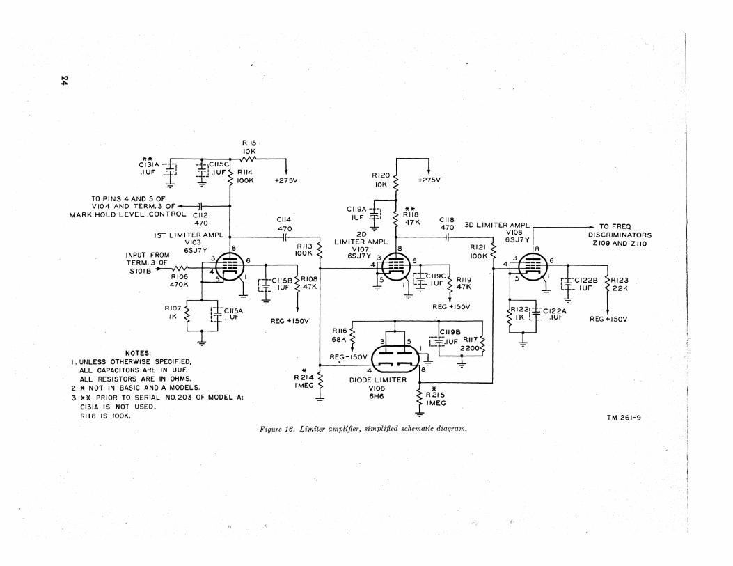
~
** CI31A ·-Xl .IUF -IJ -.::1:;CII5C -lJ .IUF
TO PINS 4 AND 5 OF VI04 AND TERM.3 OF ----l1f----4
MARK HOLD LEVEL .CONTROL CII2 470
RII5 10K
RII4 lOOK +275V
CI14
470 1ST LIMITER AMPL + I(
VI03 8
INPUT FROM 6SJ7Y TERM. 3 OF ~=~ __ \~b=-' _...-__ -. SIOIB ~~1
NOTES:
RI06 470K
RI07 IK
I. UNLESS OTHERWISE SPECIFIED, ALL CAPACITORS ARE IN UUF. ALL RESISTORS ARE IN OHMS.
-:-
2 * NOT IN BA~IC AND A MODELS.
-:-
CII5A .IUF
3. ** PRIOR TO SERIAL NO.203 OF MODEL A: CI31A IS NOT USED. RI18 IS lOOK.
Rloa 47K
REG +150V
* R214 IMEG
-:-
RII6 68K
-:-
DIODE LIMITER VI06 6H6
-=-
CII8 470 3D LIMITER AMPL ~ _____ ..
VI08 I
6SJ7Y
TO FREQ DISCRIMINATORS
Z 109 AND Z 110 RI21 < 18 lOOK
RII9 47K
REG +150V
CII9B '-X UF RII7 L:r __ 1 2200
* R215 IMEG
-:-
4
RI22r:t.-CI22A IK Lx_ .IUF
-:-
RI23 22K
REG +150V
TM 261-9
Figure 16. Limiter amplifier, simplified 8chematic diagram.
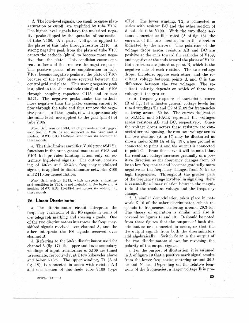
d. The low-level signals, too small to Cause plate saturation or cutoff, are amplified by tube. VI07. The higher level signals have the undesired negative peaks clipped by the operation of one section ,of tube VI06. A negative voltage js applied to the plates of this tube through resistor R1l6: A strong negative peak from the plate of tube VI03 causes the cathode (pin 4) to become more negative than the plate. This condition causes cur-
" rent to flow and thus remove the negative peaks. The positive peaks, after amplification in tube V107, become negative peaks at the plate of V107 because of the 1800 phase reversal between the control grid and plate. This strong negative peak is applied to the other cathode (pin 8) of tube VI06 through coupling capacitor 0118 and resistor, R121. The negative peaks make the catho:le more negative than the plate, causing current to flow through the tube and thus remove the nega- '
live peaks. All the signals, now at approximately he same level, are applied to the grid (pin 4) of ube V108. .
Note. Grid resistor R214, which prevents a floating-grid condition in V107, is not included in the basic and A models; MWO SIG 11-278-1 authorizes its addition to these models.
e. The third limiter amplifier, VI08 (type6SJ7Y), functions in, the same general manner as VI03 and VI07 but provides limiting action only on extremely high-level signals. The output, consisting of 50-kc and 29.3-kc frequency-moiulated signals, is applied to discriminator networks Z109 and ZllO for demodulation.
Note. Grid resistor R215, which preyents a floatinggrid con'dition in V108, is not included in the basic and A models; MWO SIG 11-278-1 authorizes its addition to these models.
26. Linear Discriminator
a.The discriminator circuit interprets the frequency variations of the FS signals in terms of d-c telegraph marking and spacing signals. One of the two discriminators interprets the frequencyshifted signals received over channel A, and the other interprets the FS signals received over channel B.
b. Referring to the 50-kc discriminator used for channel A (fig. 17), the upper and lower secondary windings of input transformer of Z109 are tuned to resonate, respectively, at a Jew kilocycles above and below 50 kc. The upper winding, Tl(A of fig. 18), is connected in series with resistor AB and one section of duo-diode tube VI09 (type
210961-52-3
6H6). The lower winding, T2, is connected in series with resistor Be and the other section of duo-diode tube VI09. With the two diode sectiom connected as illustrated (A of fig. 18), the' currents of the two circuits flow in the direction indicated by the arrows. The polarities of the vol tage drops across resistors AB and BO are positive at the ends toward the cathodes of VI09, and negative at the ends toward the plates of VI09. Both resistors are joined at point B, which is the negative side of each resistor. The two voltage
. drops, therefore, oppose each other, and the resultant voltage between points A and 0 is the difference between the two voltages. The resultant polarity depends on which of these two voltages is the greater.
c. A frequency-response characteristic curve (B of fig. 18) indicates general voltage levels for tuned windings Tl and T2 of Z109 for frequencies centering around 50 kc. The curves designated as MARK and SPAOE represent the voltages across resistors AB and BO, respectively. Since the voltage drops across these resistors are connected series-opposing, the resultant voltage across the two resistors (A to 0) may be illustrated as' shoWn under Z109 (A of fig. 19), when ground is connected to point A and the output is connected to point O. From this curve it will be noted that the resultant voltage increases gradually in a positive direction as the frequency changes from 50 kc to low frequencies and becomes gradually more negative as the frequency changes from 50 kc to high frequencies. Throughout the greater part of the frequency range involved in signaling, there is essentially a linear relation between the magnitude of the resultant voltage and the frequency change. , d. A similar demodulation takes place in net
work ZllO of the other discriminator, which responds to frequencies centering around 29.3 kc. The theory of operation is similar and also is covered by figures 18 and 19. It should be noted from these figures that the outputs of both discriminators are connected in series, so that the d-c output signals from both the discriminators add algebraically. Switch S102 in the output of the two discriminators allows for reversing the polarity of the output signals.
e. For the purpose of illustration, it is assumed in A of figure 19 that a positive mark signal results from the lower frequencies centering around 29.3 kc and 50 kc. Depending on the relative locations of the frequencies, a larger voltage E is pro-
25
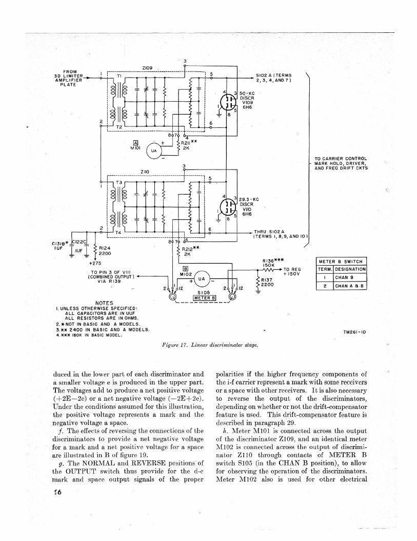
/ -'-
3
ZI09 ,I r~---T-I------------------~---·-------- ---------·i 5 SI02 A (TERMS
,-"t-,r-o----,-+--. 2, 3, 4, AND 7 )
i ,
I , ! , ! i 6
~ MIOI
3 ZIIO
r------------------------------------ ---------, 5
T3
4 3 50-KC DlSeR VI09
4
5 6H6
3 29,3 -KC DlseR
V 110 5 6H6
TO CARRIER CONTROL MARK HOLD, DRIVER, AND FREQ DRIFT CKTS
'--...-.t-O-6_---<'---t-__ TH RU S 102 A (TERMS 1,8,9, AND 10)
RI24 2200
+275
TO PIN 3 OF VIII (COMBINED OUTPUT) ----:t
VIA RI39 • ~ 2
NOTES I. UNLESS OTHERWISE SPECIFIED:
AL,L CAPACITORS ARE IN UUF ALL REsrSTORS ARE IN OHMS.
2.*NOT IN BASIC AND A MODELS. 3.** 2400 IN BASIC AND A MODELS. 4. *** ISOK IN BASIC MODEL.
RI36*** 150K
r-t----.,......'VVv-.... TO REG + 150V
RI37 2200
METER B SWITCH
TERM. DESIGNATION
I CHANB
2 CHANA a·B
TM261-IO
Figure 17. Linear discriminator stage.
duced in the lower part of each discriminator and Ii smaller voltage e is produced in the upper part. The voltages add to produce a net positive voltage (+2E-2e) or a net negative voltage (-2E+2e). Under the conditions assumed for this illustration, the' positive voltage represents a mark and the negative voltage a space.
j. The effects of reversing the connections of the discriminators to provide a net negative voltage for a mark and a net positive voltage for a space are illustrated in B of figure 19.
g. The NORMAL and REVERSE positions of the OUTPUT switch thus provide for the d-c mark and space output signals of the proper
polarities if the higher frequency components of the i-f carrier represent a mark with some receivers or a space with other receivers. It is also necessary to reverse the output of the discriminators, depending on whether or not the drift-compensator feature is used. This drift-compensator feature is described in paragraph 29.
h. Meter M101 is connected across the output of the discriminator Z109, and an identical meter M102 is connected across the output of discriminator ZllO through contacts of METER B switch S105 (in the CHAN B position), to allow for observing the operation of the discriminators. Meter M102 also is used for other electrical
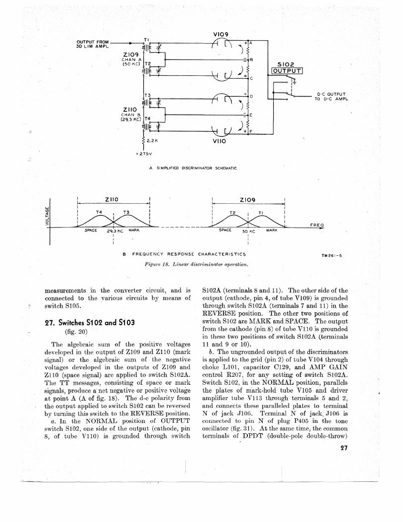
VI09 +A
") OUTPUT FROM --_+_-"""I.T1Jr-t----:------f-4 3D LIM AMPL
ZI09 CHAN A (50 KC)
ZIIO CHAN B (29.3 KC)
2.2K
+275V
VIIO
='8 )+
C
+ D
) E
)+F
5102. 10UTPUTI
I~ I I
D-C OUTPUT TO D-C AMPL
A SIMPLIFIED DISCRIMINATOR SCHEMI>,TIC
I ZI09 I ,. ·1 I I
--I----=-----"""':......t-""---~- - - - - --
i T2 ,TI ,
~ FREQ SPACE 50 KC MARK
e FREQUENCY RESPONSE CHARACTERISTICS TM261-5
Figure 18. Linear discriminfltor operation.
measurements in the converter circuit, and is connected to the various circuits by means of switch S105.
27. Switches S102 and S103 (fig. 20)
The algebraic surn of the positive voltages developed in the output of Z109 and Z110 (mark signal) or the algebraic sum of the negative voltages developed in the outputs of Z109 and Z110 (space signal) are applied to switch S102A. The TT messages, consisting of space or mark signals, produce It net negative or positive voltage at point A (A of fig. 18). The d-c polarity from the output applied to switch 8102 can be reversed by turning this switch to the REVERSE position.
a, In the NORMAL position of OUTPUT switch S102, one side of the output (cathode, pin 8, of tube V110) is' grounded through switch
i iii
S102A (terminals 8 and 11)1 The other side of the output (cathode, pin 4, of tube V109) is grounded through switch S102A (terminals 7 and 11) in the REVERSE position. The other two positions of switch S102 are MARK and SPACE. The output from the cathode (pin 8) of tube V110 is grounded .in these two positions of switch S102A (terminals 11 and 9 or 10).
b. The ungrounded output of the discriminators is applied to the grid (pin 2) of tube V104 through choke LI0l, capacitor C129, and AMP GAIN control R207, for any setting of switch S102A. Switch S102, in the NORMAL position, parallels the plates of niark~hold tube VI05 and driver amplifier tube V113 through tertninals 5 and 2, and connects these paralleled plates to terminal N of jack J106. Terminal N of jack, J106 is connected to pin N of plugP405 in the tone oscillator (fig. 31). At the same time, the common terminals of DPDT (double-pole double-throw)
27
VI09
~t"'{ TI .~
'" ~~ MARK{ · T2 I I-,..J
u- · 0 /
1 > ,-
I
· -t,,·{ I
T3 I
.~~ { E I I
T4 ) · ::E: oj MARK F 5102 u~ I-
::> Q.
VIIO I-::> 0
ZIIO
T4
/1 / I
1 I
RESISTOR
A-B B-C 0- E . E-F
TOTAL A-F
'~I ____ ~Z~I~0~9 ______ ~ I 1 T2
1 / 1 ..... -"
MARK VOLTAGE
-e}+E-e +E
-e}+E-e +E
+2E ~2e VOLTS
TI
, ........ 1 , I
I I
FREQ
SPACE VOLTAGE
-E} -E+e +e
-E} +e -E+e
-2E"+2e VOLTS
A POSITIVE MARK SIGNALS (SWITCH 5102 IN POSITION I)
;f"'{ TI
~o { :r. U'} MARK. T2 v-
VI09
-t,{ T3
~"! { G~ MARt'. T4
VIIO
5102 I-::> Q. 0-::> o
'" I-J o >
ZIIO
RE51STOR
A-B B-C
D-E E-F
TOTAL A-F
I· ZI09
TI
·1 I I I
- I --_ I FREQ
MARK VOLTAGE SPACE VOLTAGE
+e} -E+ e -E +E}+E-e -e
~~J-E+e ~n +E -e -2E + 2el£OLTS +2E-2eVOLTS
B NEGATIVE MARK SIGNALS (SWITCH 5102 IN POSITION 2) TM261- "
Figure 19. Linear discriminlttor theory diagram_
switch S104 are connected to the grid (pin 1) of tube VIn through switch S102B (terminals 8 and 11). Switch Sl02,.in the MARK position, applies a positive voltage from a regulated + 150-volt source to the grid (pin 1) of tube V111 through resistor R127 and terminals 9 and 11 of switch S102B. Switch S102, in the SPACED position, applies a positive voltage from a + 275-volt source to terminal M _of jack J106 through terminals 4 and 5 of switch 8102B, and also applies a negative voltage to the grid (pin 1) of tube V111 from a regulated -150-volt source through resistor R128 and terminals 10 and 11 of switch 8102B.
c. The d-c mark and space signals from the linear discriminator are connected through OUTPUT switch 8102 to the output control circuit (fig. 20) where they produce signals for transmission over a d-c polar or neutral telegraph. loop or over a voice-frequency carrier telegraph channel. The output control circuit (fig_ 21) consists of a driver circuit, a frequency-drift compensator circuit, and a carrier-control mark-hold circuit. A filter is connected in the input to the driver input
28
circuit (fig_ 20) to minimize the effect of noise on. the mark and space signals. Two capacitors, C125 and C126, provide for conditions of low and high signaling speed, and are added or remQved from the filter by means of the LP FIL tWitCh 8103_ These capacitors are connected in t e circuit for low signaling speeds by operating witch 8103 to the IN position. For high signaling speeds, these capacitors are disconnected from the circuit by operating. switch 8103 to its OUT position (down)_
28. Driver Circuit (fig. 21)
a_ The frequency-drift compensator circuit is connected by operating DRIFT COMPEN-8ATOR switch S104 to the IN position. The drift-compensator circuit eliminates bias efff'cts caused by frequency drifts when the drifts in both channels are in- the same direction.
b_ If the drift-compensator circuit is not used, the mark and space signals from the discriminator are connected from the contacts of OUTPUT
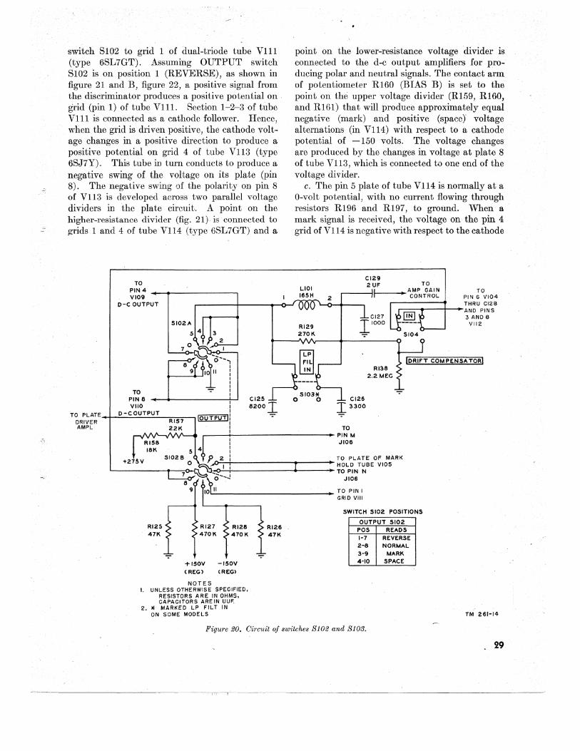
switch S102 to grid 1 of dual-triode tube V111 (type 6SL7GT). Assuming OUTPUT switch 8102 is on position 1 (REVERSE), as shown in figure 21 and B, figure 22, a positive signal from th~ discriminator produces a positive potential on . grid (pin 1) of tube Vl1l. Section 1-2-3 of tube V111 is connected as a cathode follower. Hence, when the grid is driven positive, the cathode voltage changes in a positive direction to produce a positive potential on grid 4 of tube V113 (type 6SJ7Y). This tube in turn conducts to produce a negative swing of the voltage on its plate (pin 8). The negative swing of the polarity on pin 8 of V113 is developed across two parallel voltage dividers in the plate circuit. A point on the higher-resistance divider (fig. 21) is connected to ~rids 1 and 4 of tube V114 (type 6SL7GT) and a
TO PIN 4 __ -------------, VI09
D-C OUTPUT
TO ~N8 I VIIO I
CI25
8200,J:
point on the lower:.resistance voltage divider is connected to the d-c output amplifiers for producing polar and neutral signals. The contact arm of potentiometer R160 (BIAS B) is set to the point on the upper voltage divider (R159, R160, and R161) that will produce approximately equal negative (mark) and positive (space)" voltage alternations (in V114) with respect to a cathode potential of -150 volts. The voltage changes are produced by the changes in voltage at plate 8 of tube V113, which is connected to one end of the voltage divider.
c. The pin 5 plate of tube V114 is normally at a O-volt potential, with no current flowing through resistors R196 and R197, to ground. When a . mark signal is received, the voltage on the pin 4 grid of V114 is negative with respect to the cathode
LiOI 165H
RI29 27011.
CI29 2 UF TO
TO ~----ifl----~~ ~~N;:6~ PIN 6 VI04 THRU CI28
.---:=-_---+--~AN D PIN S CI27
11000
CI26 I 3300
RI38 2.2 MEG
3 AND 8 VI12
TO PLATE-t--:;D_-.:;;.C.:;;.O..;..UT.;,.;P...;U.;,.;T_R~I~5':'7 ---, "'IO""U'"'T"'Po.UT'Pld
~R~~ER 22K I TO
--,~/'--./~"/~-- ~---+I-------------------+~ PINM
RI25 47K
5
I J~8 I I
2 I TO PLATE OF MARK .,0;::...;.------------_----- HOLD TUB E VI05 l:J:,.O-:-+------------<l------ TO PIN N
JI06
TO PIN I L-_____________________ GRID VIII
RI28 470K
RI26 47K
SWITCH SI02 POSITIONS
OUTPUT SI02 POS READS 1-7 REVERSE 2-8 NORMAL 3-9 MARK
+150V -ISOV 4-10 SPACE
(REG) (REG)
NOTES I. UNLESS OTHERWISE SPECIFIED.
RESISTORS ARE IN OHMS. CAPACITORS ARE IN UUF.
2. 1+ MARKED LP FILT IN ON SOME MODELS
Figure 20. Circuit of switches 8102 and 8103.
III
TM 261-14
29
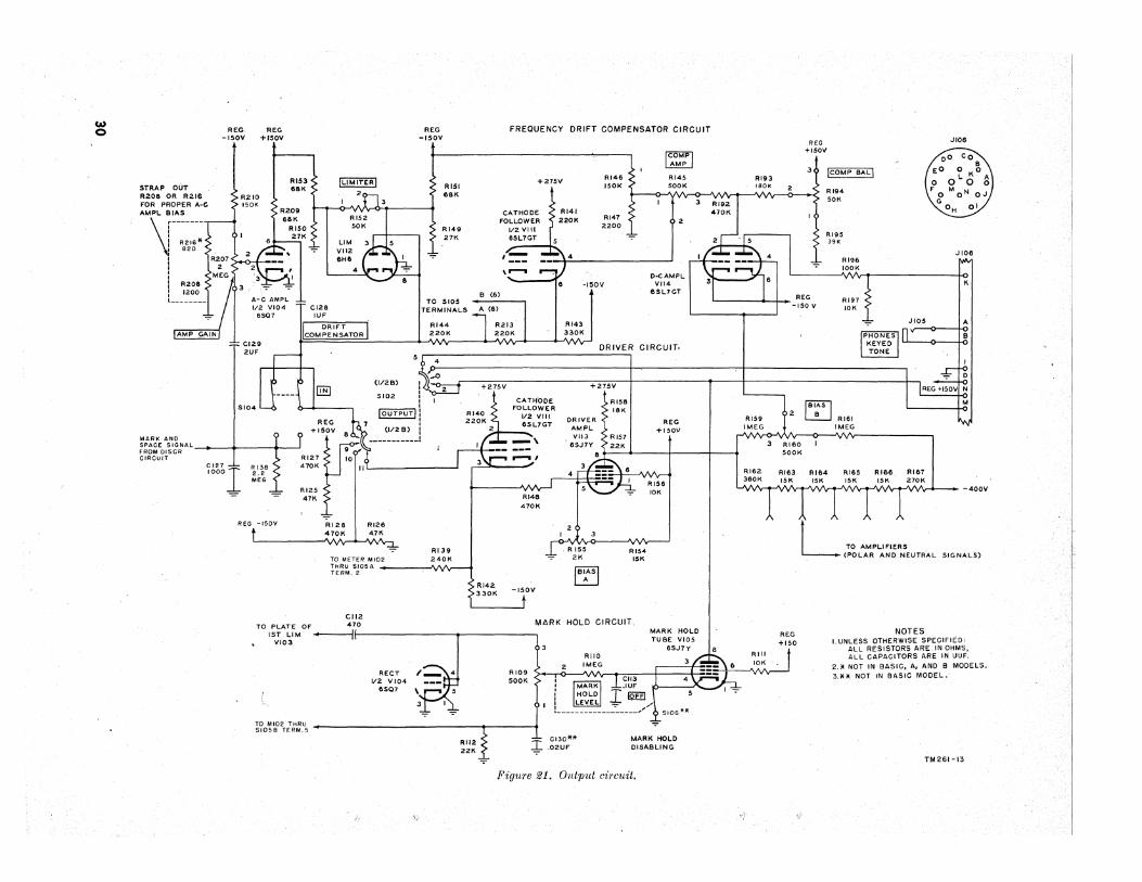
w o
STRAP OUT R20a OR R2.16 FOR PROPER A-G AMPL BIAS \ r--:~~-~ \! 820
: I : I R20a I ·1200 L _______ _
AMP
MARK AND
REG, REG -!SOV +ISOV
RI53~
R.210 ~ eak
150K R.209 68K
~:~;EDI~I;:AL_+-_-+ ___ +_-' CIRCUIT
CI271 1000 RI38 2.' MEG
REG -ISOV
REG -(SOY
FREQUENCY DRIFT COMPENSATOR CIRCUIT
ILiMITERI
2 RISI 6aK
RI49 27K
TO SI05 TERMINALS
+275V
B (6l
RI44 l R213' 220K 220K
RI28 4701<
(1/29) I SI02 I
I I
IOUTPUT)I I
(1/2 B) i -----------!
TO METER MI02 R139 240K
~~:~.S~05A ~
CII2
RI42 330K
CATHboE FOLLOWER
V2 VIII 6SL7GT
RI48
470K
-*--ISOV
REG Jloe
ICOMPI 1-ISOV
AMP
RI48 ~ RI45 ~ICOMPBAL\ 1501( SOOK . 180K 2
RI94
Riga SOK
RI.7 f ?2
410K
2200 RigS 39K
.~~ I 4 l RI9S
D-CAMPl .---. r--I lOOK
Jloe
-150V VII4 K eSL1GT
REG RI97 -150 V 10K
RI43J -1. 330K
JI05
.A
A
DRIVER CIRCUIT,
+27.5V
DRIVER AMPl Vll3
8SJ7Y
2
~ R 155
2K
IB~ASI
RI58 18.
RIS4 15K
REG +150V
RISO 10K
ISlAS I ~ IMEG IMEG
3 Rleo 500K
R112· Riel Rla4 RISS RI68 RI67 380K 15K 15K 15K I<K 270K
~~~~VV~~AI~~AI~~~~~~ .. --~-400V
L- . -TO AMPLIFIERS
(POLAR AND NEUTRAL SIGNALS)
TO PLATE OF 47.0 IS:'O~M -.-,( MARK HOLD CIRCUIT. MARK HOLD TUBE VIOS
eS.,7Y
NOTES
RECT V2 VI04
6SQ7
REG +150
~ 2 IMEG ~·'~'6. .u IO~~K' .~~ I ;~~~ I IOVV\ ,_". . t-=~
SIDell:·
~~o~!f2T;~:.U5 ---------------.,...----+
~t
RII2 22K
C130~Ut
:;j; .02UF MARK HOLD DISABLING
Figure 21. Output circuit.
,:'(t
I. UNLESS OTHERWISE SPECIFIED, ALL RESISTORS ARE.IN OHMS, ALL CAPACITORS ARE IN UUF.
2. M NOT IN BASIC. A, AND B MODELS. 3.** NOT IN eASIC MODEL.·
TM261-13
(pin 6) (from contact a~ '2 of the BIAS B potentiometer). This causes V114 to remain cut off. When the grid voltage is positive with'respect to the cathode (space signal), tube V114 conducts. Plate current from pin 5 of V114, flowing through resistors R196 and R197, produces a voltage drop across R197. This causes the voltage at pin K of receptacle JI06 to increase in a negative direction. The voltage alternations at' pin K, arising from mark and space signals,can cause an external tone-oscillator circuit (similar to the oscillator shown in figure 30) to conduct and transmit tone for a mark signal, and to cut off tone for a space s~gnal. Similar voltage variations are impressed on the lead from the lower resistance voltage divider, which includes resistors R162 to R167, inclusive. In this case, a potentiometer is not used to adjust the voltage swings, but the lead is soldered ~o a point in the voltage divider at which the alternations are plus or minus with respect to a -150 volt potential on the cathode of VI Hi. The approximately equal voltage swings from the lead connected to the lower resistance voltage divider control the d-c output circuit.
d. The polarity relationships' at the grids, cathodes and plates of the tubes in the driver circuit from a mark signal are illustrated in B of figure 22. The diagram assumes that the lower portion of each discriminator produces a positive mark output. Opposite polarities are produced for a spacing signal. OUTPUT switch S102 is turned to position 2 (NORMAL) if the upper portion of each discriminator produces a positive mark signal. The cathode potential of driver amplifier tube Vl13 can be adjusted from 0 volt to about + 17 volts by BIAS A potentiometer R155 (fig. 21). The adjustment is made to produce the O-volt transition between output mark and space signals when the grid input to V113 is o volt.
29. Frequency-Drift Compensator Circuit
a. Under operating conditions, the 50- and 29.3-kc carrier frequencies may tend to drift from nor~ mal. If no compensator equipment were provided under such conditions, the telegraphic d-c output signa,ls would be biased (distorted in relative length). To minimize the biasing effect; the output control circuit is equipped with a frequency-drift compensator circuit which may be connected to the driver circuit by operating DRIFT COMPENSATOR switch S104 to its IN
position (fig. 21). TQ connect the drift-compen.;. sator circuit, OUTPUT switch S102 must be turned to a position (NORMAL OR REVERSE) which is opposite to the regular position when the circuit is not used. This is because of the voltage. reversal introduced by the a-c amplifier (section 2-3-6 of tube VI04) which is part of the driftcompensator circuit
b. When switch S104 is turned to the IN position 2-3-6 of tube VI04 is connected to the qutput of the discriminator ahead ~f th() driver circuit to amplify the mark and space signals. The input to the grid (pin 2) of tube V104 is through coupling capacitor C129, and the output (pin 6) of this tube .to grid 1 of tube Vll1 is through capacitor C128. With this circuit arrangement, the d-c component of the discriminator output is removed so the voltage differences corresponding to mark a.nd space signals can be made symmetrical, establish- . ing a O-volt level, approximately midway between' the upper and lower voltage limits.
c. A voltage pulse corresponding to a mark or space signal is connected to the driver tubes, and is fed back to the input of the driver tubes to maintain the voltage conditions until the pulse. of the opposite-polarity (a space or mark signal) is delivered from the discriminator. The feedback circuits for locking in a signal condition include section 1-2-3 of tube V114 Ilrnd section 4-5-6 of tube Vlll. The voltage pulses produced by the discriminator are. connected through the AMP GAIN potentiometer R207 tb the grid of tube V104. The grid is biased a few volts negative by the voltage divider consisting of resistors R208 and R210 (and R216 in the C and D models). The AMP GAIN potentiometer is set at a point to provide proper voltage changes at the grid (pin 2) ofV104; for example, +.25 volt for a ml,irk and - .25 volt for a space. The amplified plttte-voltage variations might be, for example, ± 15 volts, centered about a potential of + 80 volts.
d. Capacitor CI28 eliminates the d-c component of the voltage changes at the plate of V104, thus impressing pulses in the order of ± 15 volts on' grid 1 of tube Vln. The' pulses at the cathode of tube VIII are coupled to the grid (pin 4) of V113 through resistor R148, thereby driving the grid of tube V:H3 momentarily positive. When the grid of tube V113 is driven more positive, the tube plate current will increase, thereby lowering the voltage at the plate and,' in turn, causing the potential at the slide arm of potentiometer R160 (BIAS B) to become more negative.
31
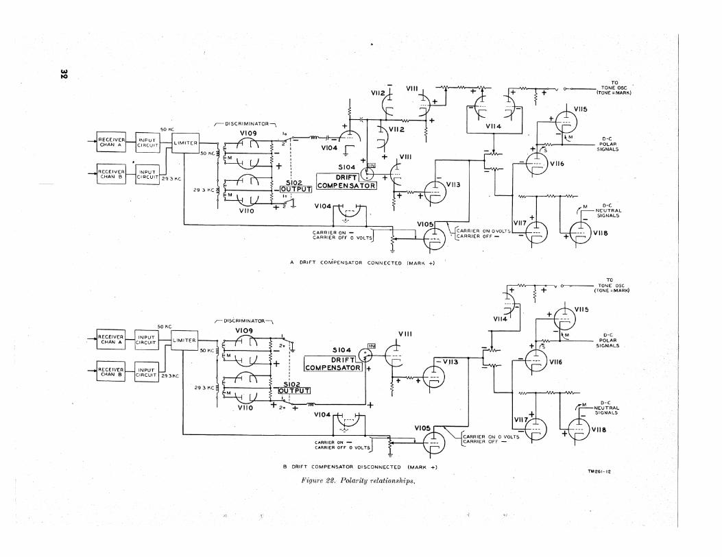
Co\) N)
r-DISCRIMINATOR, l~ 09 10
~ ---. - -- , -
VI04 .r
VIIO
A DRI,T COMPENSATOR CONNECTEO (MARK +)
,.- DISCRIMINATOR""
20 : ~ ,
VIII
'-~+ :
VIIO
,
, : ,
5102 IOlJiPUTJ
i_ : +20 +
VI04
B DRIFT COMPENSATOR DISCONNECTED (MARK +)
Figure 22. Polarity relationships.
VII3
CARRIER ON OVOLT5 CARR.IER OFF -
1!J
VII6
D-C POLAR,
SIGNALS
D-C NEUTRAL SIGNALS
VII8
TO .. 0 TONE osc + (TONE=MARK)
D-C POLAR
SIGNALS
D-C NEUTRAL SIGNALS
Vll8
TMe61-12
Because the slider arm of potentiometer RI60 is directly connected to grid 1 of tube V114, this tube will conduct less, and the voltage at its plate and at the slider arm of potentiometer RI45 (COMP AMP) will increase. The slider arm of potentiometer R145 is connected to grid 4 of tube Vl11, a cathode follower. When the grid of the cathode follower is driven positive, the cathode will also be more positive and because the cathode is connected' to grid 1 of tube VIII through resistors R213 and R144 and through switches S104 and S102, the grid (pin 1) of tube Vll1 will be held positive, even after the duration of the positive pulse from the plate of tube VI04. Thus, the positive pulse, corresponding to a mark signal, will lock the driver circuit in the mark condition until a negative (space) signal is received. The negative pulse output from the plate (pin 6) of tube VI04, corresponding to a space signal, will drivfl grid 1 of tube VIII negative, thereby reversing the polarities througout the drift compensator circuit, and providing a negative voltage at cathode 6 of tube VIII to hold the driver circuit in the space condition.
e. The COMP BAL and COMP AMP potentiometers are adjusted to produce ± I5-volt variations at grid 1 of tube Vlli (assuming that signal pulses in the order of ± 15 volts are transmitted through capacitor CI28). The COMP BAL potentiometer adjusts the voltage variations on plate 2 of V114 to produce equal mark and space swings, while the COMP AMP potentiometer adjusts the gain through section 4-5-6 of tube VIII to provide the proper voltage levels' at cathode 6; for example, ± 15 volts for mark and space signals. Meter B is connected across resistor R2I3 when METER B switch 8105 is turned to the COMP AMP position. If the drift-compensator circuit is adjusted properly, the plate swings of tube VI04 and the feedback voltage at cathode 6 of VIII are equal, as indicated by zero or small deflections of meter B when miscellaneous signals arc received.
f. The foregoing information shows that, in response to a momentary pulse of mark-signal voltage (+15 volts), the feedback path produces a steady state potential of about + 15 volts which locks until a space voltage pulse of the same magnitude, but of opposite polarity (-15 volts), is received. The circuit then locks in a similar manner for the space condition and awaits a mark pulse to unlock it. It is possible occasionally for a transmitted steady signaling
210961-52---4
condition (either mark or space) to change without unlocking the voltage established by the driftcompensator circuit. This can occur during testing or adjusting procedures, and results in the first signal-voltage pulse being of the same polarity as the locked-in voltage. The first signal-voltage pulse is, therefore, ineffective. Because of the time constant of the circuit, a comparatively long time is required to discharge capacitor C128 to a vpltage low enough for a single-voltage transition to unlock the circuit. Several voltage transitions, therefore, may be lost if the signal speed is rapid. Limiter V112 (type 6H6) a duo-diode, protects the circuit against such a condition by clipping the peaks of pulses exceeding a maximum value of about ± 15 volts, as determined by the setting of the LIMITER potentiometer. This arrangement of limiting the maximum voltage of the pulse signals minimizes the length of time required to resume normal keyiI).g. The LIMITER potentiometer is connected across the cathode (pin 4) and plate (pin 5) of tube V112, and between positive and negative voltages of two voltage dividers consisting of resistors R150 and ~153, and resistors R149 and RI51, respectively.
30. Carrier-Control Mark-Hold Circuit
a. The purpose of the carrier-control mark-hold circuit shown in the IQwer part of figure 21 is to hold a mark signal on the TT loop circuit should the incoming carrier fail or be ShJlt off for any
. reason. As long as an incoming carrier signal is received over the radio link, a 50- and 29.3-kc frequency-shifted signal voltage will appear at the output of tube VI03. The carrier voltage is. applied to the duo-diode portion of dual-purpose tube VI04. The diode elements of VI04 shunt the positive peaks of the 50- and 29.3-kc carrier to ground, and establish a negative potential on grid 4 of V105 (type 6SJ7Y). Under this condition, no plate current flows in tube VI05 and the tube has no effect upon the mark and space signals produced by driver tube V113. If, for any reason, the r-f carrier fails, the 50- and 29.3-ko carriers reduce to zero and the negative voltage on .grid 4 of tube VI05 is reduced to zero. Tube VI05, therefore, will conduct and produce the same effect at the plate (pin 8) of driver tube V113 as exists when a mark signal is transmitted through the driver cirquit. This condition is maintained as long as the carrier is shut off, but is removed automatically as soon as the carrier is again received.
33
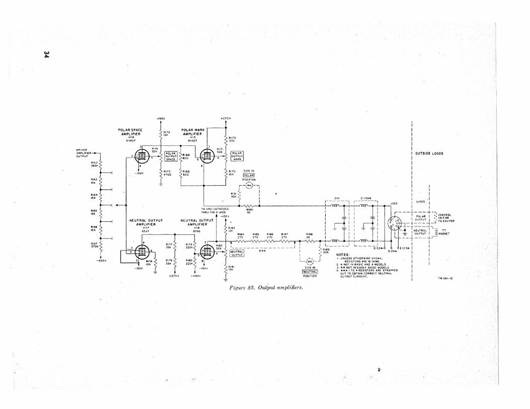
w
"""
ORIVER AMPLIFIER OUTPUT
RIG2 3601<
RIG3
'"
RI64
'" RIGS '5,
RIG6
'5K
RIG7 2701<
-400V
-150\1
POLAR SPACE AMPLIFIER
'0'116 GVGGl
NEUTRAL OUTPUT AMPLIFIER
Vl17
6SJ7
fillS
'0'
RI7l
'" RI7S
'" +27'5V
POLAR MARK AMPLIFIER
'0'115
6v6GT
+2:75V
RI70
'"
POSITION
r-{;;}--' ,_.... I
i I RI91 <) t 301< <~ I
I I
TO V401 CATHOOES RI90 THRJ PIN H JI06 30
NEUTRAL OUTPUT AMPLIFIER
RI79 2201<
-150V
RISS 2'0
RIS6 270
RI87 270
I I
ZIII r-----'
I
2113** ,------,
, I I I I I I I OUTSIDE LOADS
I I I I I I I I I I I I I ,I I LINES t
I I ,---1.---+-,
I POLAR I :> ~~~TT~~L I OuTPUT I ,~ FS EXCITER
-t---:::l-~
- T N-;;R~L I-L;;; TT I OUTPUT I ;~ MAGNET
--f----lFJ I I
I '} 301<
I "
"23* I II [124* I
I I 1'118.0 2201<
-150y
-400V
fHal
'0'
I __ [;A .... \_ J ,j
$105 IN
INEUTRALI
POSITION
Fig'ure 28. Output amplifiers.
NOTES, L UNLESS OTHERWISE SHOWN,
RESISTORS ARE IN OHMS Z * NOT IN BASIC AND A MODELS. 3. ** NOT IN EARLY BASIC MODELS 4. *** I TO 4 RESISTORS ARE STRAPPED
ouT TO OBTAIN CORRECT NEUTRAL OUTPUT CURRENT.
'#
I I I I I I I TM 261-15
b. In the lettered models, switch Sl06 is provided no disable the mark-hold circuit. It is ' .operated by a cam mechanism on the shaft of MARK HOLD LEVEL control (Rl09). Turning the control fully counterclockwise opens S106. Normally, Sl06 is in the closed position, and in this position the cathode Of tube Vl05 is connected to ground. Operating this switch to the open position opens the cathode circuit of VI05 and makes the tube inoperative. This position of the switch is desirable during adjustment of the equipment and when receiving weak signals, for at these times increased sensitivity is required.
31. D·C Output Circuit
. a. General. The d -c output amplifier tubes. (fig. 23) convert the output of the driver circuit into polar and neutral telegraph signals. Two tubes, V1l5 and VIJ6 (type 6V6GT), are lIsed to produce the polar signals and two other tubes, V1l7 (type 6SJ7) and V118 (type 6Y6G) , are used to produce the neutral signals. The input to the control grids of tubes V116 and V117 is from a point on the voltage divider in the plate circuit of tube V1l3 (fig. 21) where essentially equal plus and minus alternations are proquced. This point. on the voltage divider is determiued by voltmeter tests. The voltage on this lead is negative with respect to the -I 50-volt potential OIl the cathode of the two tubes when a mark signal is transmitted, and positive with respect to this potential when a space signal is transmitted (fig. 22). The alternation of the voltage from plus to minus is controlled by driver tube V1l3.
b. Polar Signals. (1) Polar output tubes VllG and V115 are
connected in such a manner that one tube conducts while the other tube is cut off and vice' versa. The voltage on control grid 5 of tube V116, as shown in figure 22, is minus (-) for a mark signal and plus (+) for a space signal.
(2) When a mark signal is transmitted, the minus potential on the control grid .of tube'V116 cuts off this tube. Therefore, the plate current from V116 stops flowing through resistors RI69 and Rl68 (fig. 23), putting both ends of these resistors at the same potential. Since the control grid and the cathode of tube V115 are connected to the ends of these resistors, tubeV115 conducts. The elec-
tron path is from the +275-volt supply to ground (pin A .of JI03)i through the line to the outside load (or control unit), and back to pin B of JI03, thence through filters Z113 and Zill and resistor Rl90 to the cathode of VII5, and through the tube to the +275-volt supply. When V115 conducts, it presents a relatively low resistance to the flow of electrons from the ground to the + 275-volt supply. This effectively places approximately + 275-volts at pin B at Jl03. The screen-grid voltage oftube V115 is varied by potentiometer Rl71 (POLAR OUTPUT MARK), which is connected as part of a voltage-divider circuit with' resistors R170 and R172. This potentiometer is adjusted to produce a mark output current of approximately + 25 rna.
(3) When a space signal is transmitted, the d-c output voltage from V1l3 is positive with respect to the -150 volts on the cathode of V116 so that tube V1l6 conducts. The plate-current flow is from the -I50-volt supply to the V1l6 cathode, through V116, from plate pin 3 through resistors RI69, RI68, and RI90, through filters Z111 and Z113 to pin B of JI03, out over the line to the load (or control unit), then baek over the line to pin A of J103, and thence to ground in the power supply of the converter unit. The voltage drop thr.ough resistors RI68 and R169 produces a negative grid bias for tube V115 sufficiently high to cut off that tube. The. screen voltage of tube V116 is adjusted by potentiometer RI74 (POLAR OUTPUT SPACE) which is connected as part of a voltage-divider circuit which includes resistors RI73 and RI75. This potentiometer is adjusted to pr.oduce a space output current of approximately 25 rna.
(4) The polar currents which flow through filter Zill (in the C and D models, to a second filter, Z113) to pin B of JI03 also pass through shunt resistor RI90 which is across meter MI02. Meter MI02 is connected in series with resistorR19l and will read milliamperes directly when METER B switch S105 is set in the POLAR position. The
35
function of filters Zlli and Z1l3 is to reduce any extraneous noise that may be picked up by the control line between JI03 and the load or control unit.
c. Neutral Signals.
36
(1) Tubes VIl7 and V1l8 alternately conduct and cut off to produce neutral telegraph signals. When a mark signal is transmitted, a negative voltage potential is connected from the output of driver tube V1l3 to the control grid of tube V117. This voltage is sufficient to cut off tube V117. The plate voltage for tube VII7 and the grid voltage for tube V118 are obtained from separate points on a voltage divider consisting of resistors RI77, RI78, RI79, and RI80 in series across the +275-volt and -400-volt supplies. This arrangement produces 3, voltage at the control grid of VI18 which is positive with respect to the cathode voltage when tube VII7 is cut off, and negative when tube VII7 is conducting.
(2) When tube V1l7 is cut off, tube V118 conducts. The electron flow leavp,s the -I50-volt supply, flows through V1l8 and then, from the plate (pin 3) of VI18, flows through resistors R184, RI85, R186, RI87, and RI88, then through filters Zfll and Z1l3 to pin D of JI03, out through the line to the TT equipment, back through the line to pin E of J103, and thence through ground in the converter unit to the -I50-volt supply. When tube V1l8 conducts, it presents a very small resistance to the flow of plate current, and because its cathode is tied to -150 volts, pin D at J103 in effect assumes the same potential of -150 volts. The four resistors, R184 to R187 inclusive, are not strapped out if the TT is located withill the radio receiving station. By strapping out resistors R184 to RI87, the station can be located at the end of a circuit not exceeding 1,800 ohms resistance (equivalent to about a mile of 19-9age cable). Resistor R188 acts as a meter shunt for meter MI02. M102, in series with multiplier R189, is connected across meter shunt R188 to indicate directly in milliamperes when METER B switch
S105 is set on NEUTRAL (position 4). The screen-grid voltage of tube V118 is adjustable by means of potentiometer R182 (NEUTRAL OUTPUT) which is connected as part of a voltage-divider circuit (in series with resistors RI81 and R183). This control is provided to adjust the neutral loop current to a value of approximately 60 ma for mark signals.
(3) When a space signal is transmitted, tube V117 conducts, causing the voltage at the grid of V1I8 to go sufficiently negative to .cut off the tube. With V118 cut off, no current flows in the neutral output circuit.
d. Oonnections. In the B through D models, three additional binding posts are added on the rear of the unit. These binding posts, E122, E123, and E124, are connected respectively to terminal 2 of suppressor filter Z1l3, pins A and E of jack J103, and to terminal 4 of suppressor filter Z1l3. Neutral and polar connections can be m'ade directly to the converter through these connections. When the special cords for the converter unit. (such as those included with Radio Set AN/MRC-2) are unavailable, these binding posts may be used.
32. Metering Circuits
The frequency-shift converter is provided with microammeters M101 and M102 for checking the operation of the various circuits. Meter MIOI is connected permanently, in series with current limiting resistor R2Il, across terminals 7 and 8 (output) of discriminator ZI09. This meter measures the channel A discriminator output current (fig. 17). Meter MI02 is connected to terminals 12 of the A and B sections of METER B switch S105. This switch has the following 11 positions (fig. 24):
a. CHAN B Position. In position ·1, meter MI02 measures the relative discriminator output from channel B (transformer ZIlO). It is connected, in series with current limiting resistor R212, across terminals 7 and 8 of ZllO.
b. CHAN A + B Position. In position 2, meter MI02 provides a relative indication of the cathode current of VIllA. This current is eomposed of the added outputs of both the A and B channels. The voltage applied to the grid of driver amplifier VII3 is directly proportional to this cathode current.
c. POLAR Position. In position 3, meter MI02
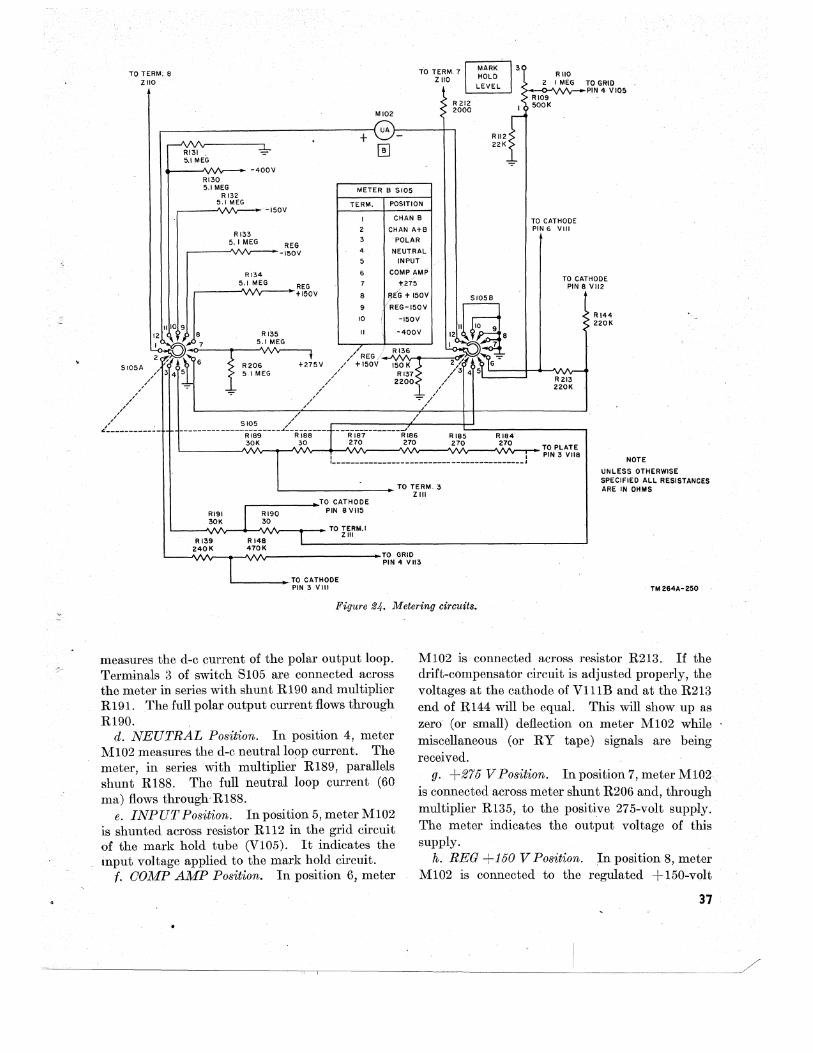
:::-
TO T Z
SIOSA
fRM; 8 TO TERM. 7\ MARK ~I HOLD
110 ZIIO LEVEL
S: R 212 I
MI02 2000 r--'
UA R1I2~ ~.
+ -4=- ill 22K';>
5.1 MEG -=?-, -400V
RI30 5.1 MEG METER B 5105
RI32 5.1 MEG
'"ISOV TERM. POSITION
I CHAN B
RI33 2 CHAN A+B
5.1 MEG 3 POLAR REG
-ISOV 4 NEUTRAL 5 INPUT
RI34 6 COMP AMP
5.1 MEG 7 +.215 ~~r5GOV a ~_ t ISOV SIOSB
9 REG-ISOV
10 ! -ISOV 11 109 ,~ 12rf#a
RI3S II \ -400V 12 a
~ 7 5.1 MEG L!.o. 7
2~ is 'v +Jsv // REG/ RI36 ...;, -
< R206 / +150V ISOK 2:1- 4i~' 6-,/' :3 4 5 51 MEG / 2R21g~ •
,/3 / /
,
"*" / , , / ~/ , - /
7 ' S~ / ' --- --------------~~iir---·--:~~ii---l--~~7--------~~; Rl8S RI84
270 270
I I I __________________________________________ J
TO TERM. 3 ZIII
TO CATHODE
RI91 r RI90 PIN a VIIS
30K 30 TO TERM. I
T ZIII RI39 RI4a
140K 470K TO GRID vv PIN 4 VII3
,TO CATHODE PIN 3 VIII
Figure 24. Metering circuits.
RIIO ~ I MEG T
'V P RI09
o GRID IN 4 VIOS
500K
TO CATHODE PIN 6 VIII
TO CAT HODE VII2 PIN a
.(
A
R213 220K
TO PLATE PIN 3 vila
RI44 220K
NOTE
UNLESS OTHERWISE SPECIFIED ALL RESISTANCES ARE IN OHMS
TM264A-250
measures the d-c purrent of the polar output loop. Terminals 3 of switch 8105 are connected across the meter in series with shunt R190 and multiplier R191. The full polar output current flows through R190.
d. NEUTRAL Position. In position 4, meter M102 measures the d-c neutrallo9P current. The meter, in series with multiplier R189, parallels shunt R188. The full neutral loop current (60 ma) flows through-R188.
M102 is connected across resistor R213. If the drift-compensator circuit is adjusted properly, the voltages- at the cathode of V111E and at the R213 end of ~144 will be equal. This will show up as zero (or small) deflection on meter M102 while miscellaneous (or RY tape) signals are being received.
e. INPUT Position. In position 5, meter M102 is shunted across resistor R112 in the grid circuit of the mark hold t1.lbe (V105). It indicates the Input voltage applied to the mark hold circuit.
f. COMP AMP Position. In position 6, meter
g. +275 V Position. In position 7, meter M102\ is connected across meter shunt R206 and, through multiplier R135, to the positive 275-volt supply. The meter indicates the output voltage of this supply.
h. REG +150 V Position. ,In position 8, meter M102 is connected to the regulated + 150-volt
37
~~----------------~"~I--------------------~----------~~
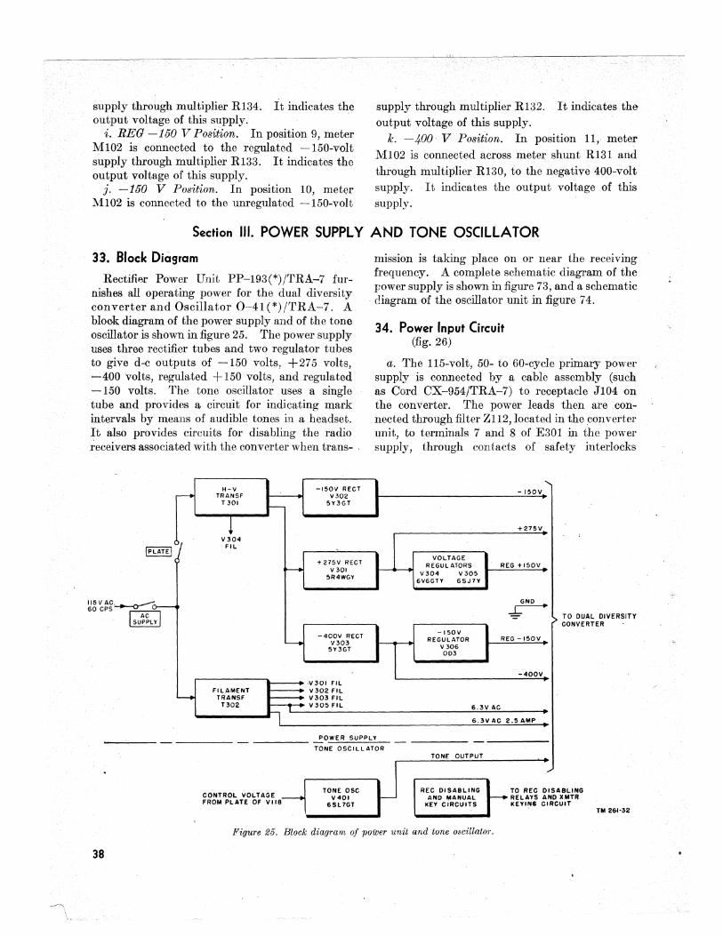
supply through multiplier R134. It indicates the output voltage of this supply.
i. REG -150 V Position. In position 9, meter M102 is connected to the regulated -150-volt supply through multiplier R133. It indicates the output voltage of this supply.
j. -150 V Position. In position 10, meter MI02 is connected to the unregulated -150-volt
supply through multiplier R132. It indicates the output voltage of this supply.
k. -400 V Position. In position 11, meter MI02 is connected across meter shunt R13l and through multiplier R130, to the negative 400-volt supply. It indicates the output voltage of this supply.
Section III. POWER SUPPLY AND TONE OSCILLATOR
33. Block Diagram RectifiBr Power Unit PP-193(*)jTRA-7 fur
nishes all operating power for the dual diversity converter and Oscillator 0-4l(*)jTRA-7. A blook diagram of the power supply and of the tone oscillator is shown in figure 25. The power supply uses three rectifier tubes and two regulator tubes to give d-c outputs of -150 volts, +275 volts, -400 volts, regulated + 150 volts, and regulated -150 volts. The tone oscillator uses a single tube and provides a circuit for indicating mark intervals by means of audible tones in a headset. It also provides circuits for disabling the radio receivers associated with the converter when trans- .
~
LATE
115 VAG. _ _ ----' c----< 60CPS~~ C
AC SUPPL y
L...,
H-V TRA"SF
T 301 -
VJ04 FIL
FILAMENT TRANSF
T302
~
-150V REeT V302
5Y3GT
+ 275V REGT
~ v 301 SR4WGY
-400V REGT
'----* V303 5Y3GT
·V301 FlL V302 FIL V303 FIL V30S FIL
mission is taking place on or near the receiving frequency. A complete schematic diagram of the power supply is shown in figure 73, and a schematic diagram of the oscillator unit in figure 74.
34. Power Input Circuit (fig. 25)
a. The l15-volt, 50- to 50-cycle primary power supply is connected by a cable assembly (such as Cord CX-954jTRA-7) to receptacle JI04 on the converter. The power leads then are .connected through filter Z112, located in the converter unit, to terminals 7 and 8 of E301 in the power supply, through contacts of safety interlocks
"-- 150V
+275V
VOLTAGE REGUL ATORS REG+ISOV
V304 V30S 6V6GTY 6SJ7Y
~ND •
-ISOV REGULATOR REG -ISOV
V306 003
-400V
6.3VAC
6.3VAC 2.SAMP
> TO OUAL DIVERSITY CONVERTER
POWER SUPPLY -
38
- -TONE OSCILL ATOR
~~~JRp~LATVEO~~Ae~'8--.1 TONE OSC
V401 r--6SL 7GT
-TONE OUTPUT
REC DISABLING AND MANUAL
KEY CiRCUITS
,.
TO REC DIS ABLING XMTR UIT -- ~~~t,:: ~,~~
Figure 25. Block diagram of power unit and tone oscillator.
TM 261-32
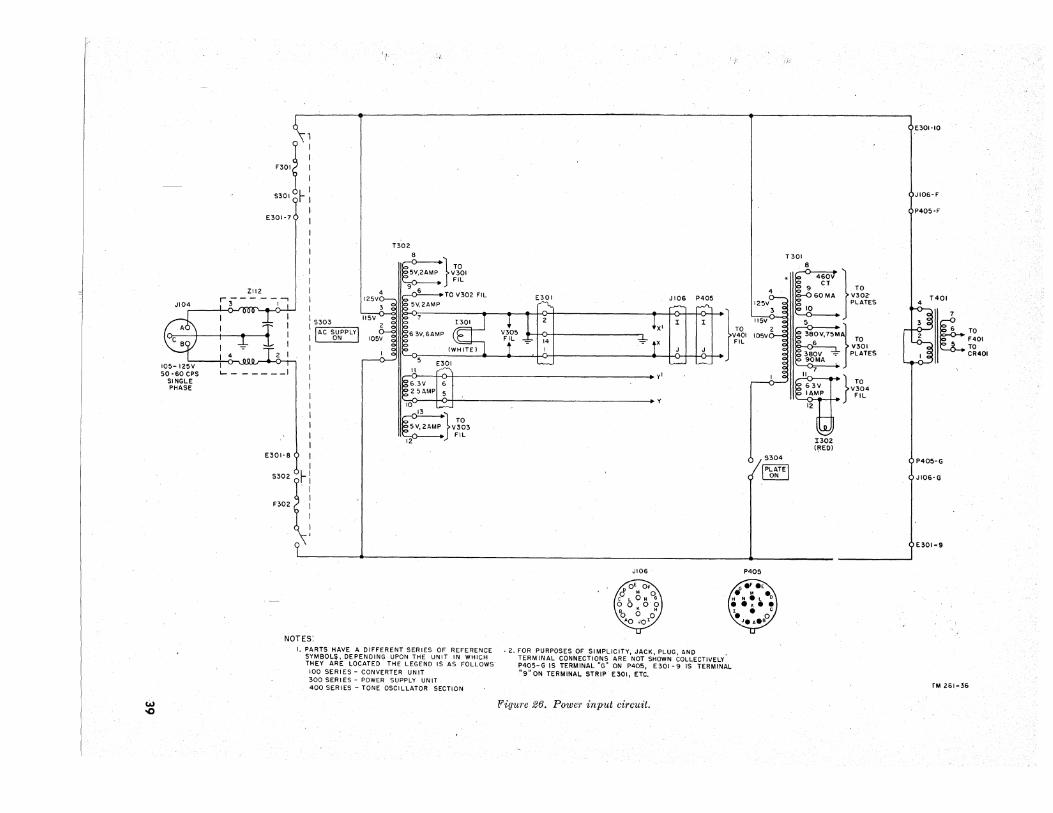
W -0
105-125V 50-60 CPS
SINGLE PHASE
'l" If IA
""~ S301 -f-
E301-7
T302
nOI 8
8
E·2AMP:}}l'01 FIt:
ZII2 r-------,
3 I ~TOV302FIL JI06 P405 }
TO V302 PLATES
r
1 S303
: lAC SoU:PLYI
1
}~
5 TO
V401 380VI 75MA FIL 6 TO
,wn".. • I ' I • IO-H--<>-f-.. }V301 -0, - 0 .. 380V ~ PLATES 90MA
-0:----+ L.. ______ I 1 1 1 ~ :' ~}TO -6.3V 6 1 1 1 1
1 1 I
25AMP 5 Y
I~} E301-8 I
1
i~ V~~3 12
S302 -f- 1
"'t NOTES:
I. PARTS HAVE A DIFFERENT SERIES OF REFERENCE SYMBOL$, DEPENDING UPON THE UNIT IN WHICH THEY ARE LOCATED THE LEGEND IS AS FOLLOWS'
100 SERI ES - CONVERTER UNIT 300 SERIES - POWER SUPPLY UNIT 400 SERIES - TONE OSCILLATOR SECTION
JI06
·2. FOR PURPOSES .OF SIMPLICITY, JACK, PLUG, AND • TERMINAL CONNECTIONS ARE NOT SHOWN COLLECTIVELY P405-G IS TERMINAL "G" ON P405, E301'9 IS TERMINAL "9" ON TERMINAL STRIP E301, ETC.
li'igure 26. Power input circuit.
S304
IPLATEI ON
P405
1302 (~ED)
. V304 FIL
£301-10
JI06-F
P40S-F
4 T401
P405-G
JI06-G
£301-9
TM 2SI-!S
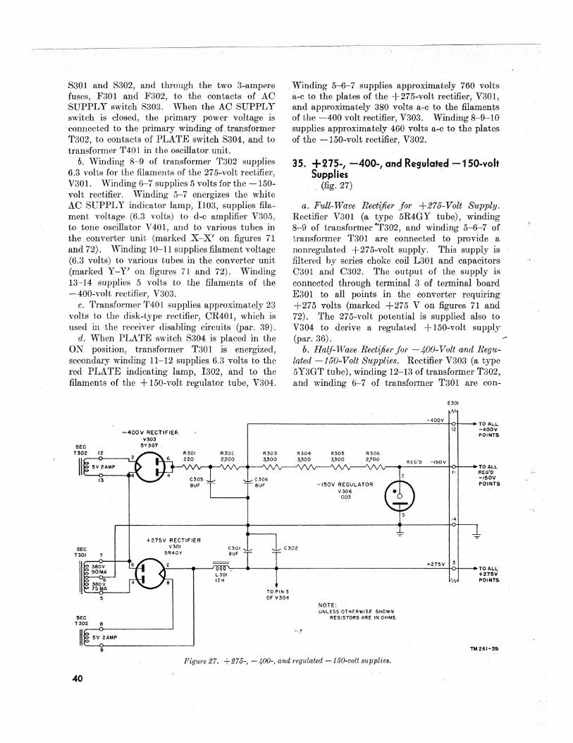
8301 and S302, and through the two 3-ampere fuscs, F301 and F302, to the contacts of AO SUPPLY switch S303. When the AO SUPPLY switch is closed, the primary power voltage is connected to the primary winding of transformer '1'302, to contacts of PLATE switch S304, and to transformer 1'401 in the oscillator unit.
b. Winding 8-9 of transformer '1'302 supplies 6.3 volts for the filamen1B of the 275-volt rectifier, V30I. Winding 6-7 supplies 5 volts for the -150-volt rectifier. Winding 5-7 energizes the white AO SUPPLY indicator lamp, I103, supplies filament voltage (6.3 volts) to d-c amplifier V305, to tone oscillator V 401, and to various tubes in the converter unit (marked X-X' on figures 71 and 72). Winding 10-11 supplies filament voltage (6.3 volts) to various tubes in thc converter unit (marked Y - Y' on figures 71 and 72). Winding 13-14 supplies 5 volts to the filaments of the --400-volt rectifier, V303.
c. Transformer '1'401 supplies approximately 23 volts to the disk-type rcctifier, OR401, which is used in the receiver disabling circuits (par. 39).
d. When PLATE switch S304 is placed in the ON position, transformer '1'301 is energized, secondary winding 11-12 supplies 6.3 volts to the red PLATE indicating lamp, I302, and to the filaments of the + 150-volt regulator tube, V304.
-400V RECTIFIER V303
5Y3GT
Winding 5-6-7 supplies approximately 760 volts a-c to the plates of the +275-volt rectifier, V301, and approximately 380 volts a-c to the filaments of the -400 volt rectifier, V303. Winding 8-9-10 supplies approximately 460 volts a-c to the plates of the -:--I50-volt rectifier, V302.
35. +275-, -400-, and Regulated -150-volt Supplies .
(fig. 27)
a. Full-Wave Rectifier jar +275-Volt Supply. Rectifier V30l (a type 5R4GY tube), winding 8-9 of transformer "'1'302, and winding 5-6-7 of transformer '1'301 are connected to provide a nonregulated +275-volt supply. This supply is filtered by series choke coil L301 and capacitors 0301 and 0302. The output of the supply is connected through terminal 3 of terminal board E301 to all points in the converter requiring + 275 volts (marked + 275 V on figures 71 and 72). The 275-volt potential is supplied also to V304 to derive a regulated + 150-volt supply (par. 36).
b. Half-Wave Rectifier jar -4-00-Volt and Regulated -150-Volt Supplies. Rectifier V303 (a type 5Y3GT tube), winding 12-13 of transformer '1'302, and winding 6-7 of transformer '1'301 are con-
SEC T301
+275V RECTIFIER V301 C301
auF C302
5R4GY
5
SEC n02 8
\1 5V 2AMP
9
40
+275V 3 ~~~--~~----------------------------~~-KH---+TOALL
TO PIN 3 OF V 304
NOTE: UNLESS OTHERWISE SHOWN
RESISTORS ARE IN OHMS.
Figure 27. + 275-, - 400-, and regulated -J50-volt supplies.
+275V POINTS.
TM 261-39.
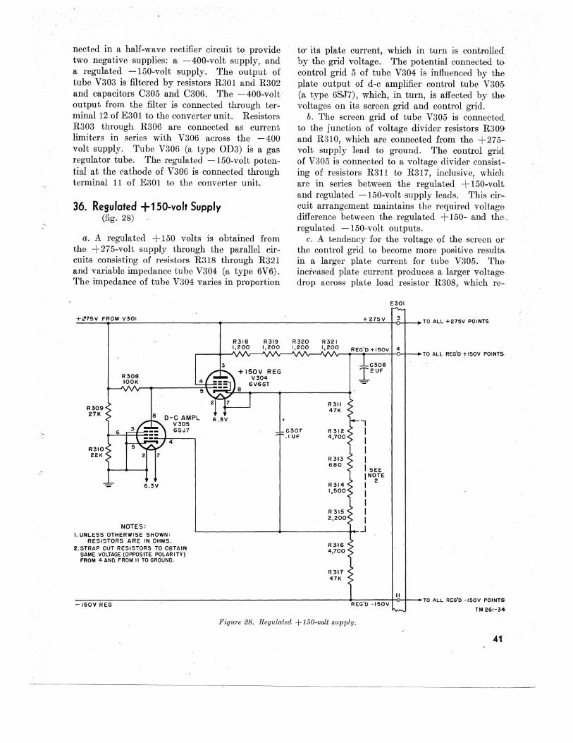
.,'
nected in a half-wave rectifier circuit to provide two negative supplies: a. -400-volt supply, and a regulated -150-volt supply. The output of tube V303 is filtered by resistors R30l and R302 and capacitors 0305 and 0306. The -400-volt output from the filter is connected through terminal 12 of E30l to the converter unit. Resistors R303 through R306 are connected as current limiters in series with V306 across the -400 volt supply. Tube V306 (a type OD3) is a gas regulator tube. The regulated -150-volt potential at the cathode of V306 is connected through terminal 11 of E30I to the converter unit.
36. Regulated + 150-volt Supply (fig. 28)
a. A regulated + 150 volts is obtained from the +275-volt supply through the parallel circuits consisting of resistors R3l8 through R32l and variable impedance tube V304 (a type 6V6). The impedance of tube V304 varies in proportion
+2'75V FROM V301
R318 R319 1,200 1,200
3 + 150V REG
R308 V304 lOOK 6V6GT
R309 27K
6.3V
4 R310 22K
- 6.3V
NOTES: I. UNLESS OTHERWISE SHOWN:
RESISTORS ARE IN OHMS. 2.STRAP OUT RESISTORS TO OBTAIN
SAME VOLTAGE 10PPOSITE POLARITY) FROM 4 ANn FROM II TO GROUNO.
,-150VREG
to'" its plate current, which. in turn is controlled by the grid voltage. The potential connected tocontrol grid 5 of tube V304 is influenced by the plate output of d-c amplifier control tube V30~ (a type 6SJ7) , which, in turn, is affected by the voltages on its screen grid and control grid.
b., The screen grid of tube V305 is connected to the junction of voltage divider resistors R30~ and R3l0, which are connected from the +275-volt supply lead to ground. The control grid of V305 is connected to a voltage divider consisting of resistors R3Il to R3l7, inclusive1 which are in series between the regulated + 1 50-volt and regulated -150-volt supply leads. This cir~ cuit arrangement maintains the required voltage difference between the regulated + 150- and the, regulated -150-volt outputs.
c. A tendency for the voltage of the screen or the control grid to become more positive resultS. in a larger plate current for tube V305. Theincreased plate current produces a larger voltagedrop across plate load resistor R308, which re-
E301
+ 275V 3 TO ALL +275V POINTS
R320 R321 1,200 1,200
TO ALL REG'O 1'150V POINTS
0308
J2UF
R311 47K
-, 0307 R312 I ,I UF 4,700
I
I R 313 I 680
I SEE INOTE
R314 I 2 1,500
I
I R 315 I 2,200 I
.J
R316 4,700
R317 47K
II
REG'O -150V TO ALL REG'O -ISOV POINTS
TM 261-34
Figure 28. Regulated + 150-volt supply.
41
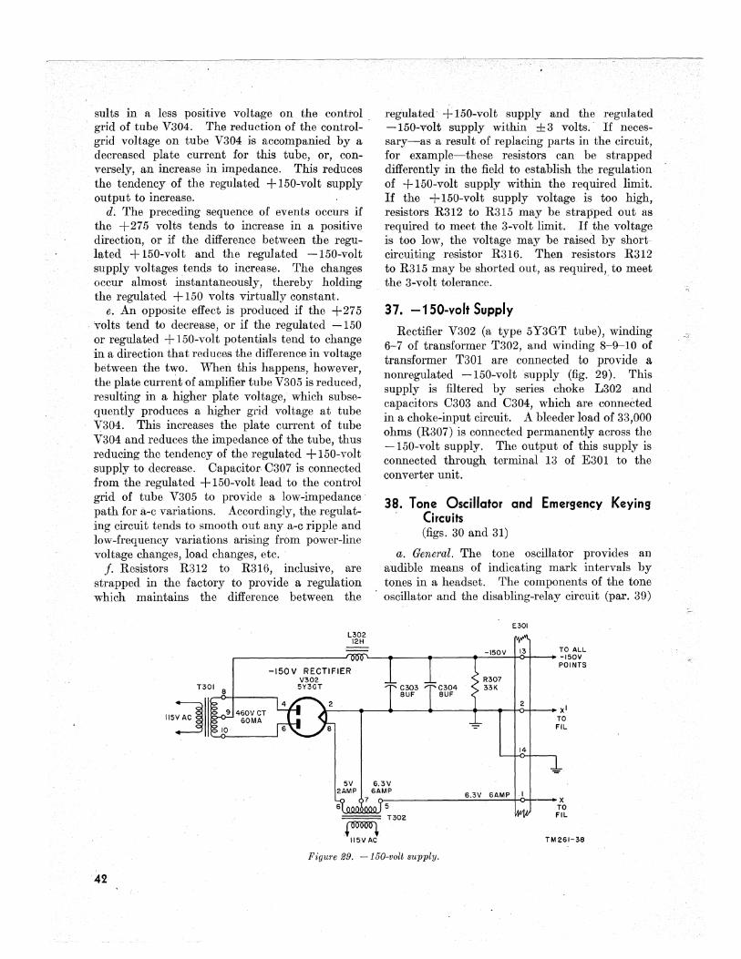
sults in It less positive voltage on the conttol grid of tube V304. The reduction of the controlgrid voltage on tube V304 is accompanied bya decreased plate current for this tube, or, conversely, an increase in impedance. This reduces the tendency of the regulated + 1 50-volt supply output to increase.
d:, The preceding sequence of events occurs if the +27.5 volts tends to increase in a positive direction, or if the difference between the regulated + l50-volt and the regulated -150-volt supply voltages tends to increase. The changes occur almost instantaneously, thereby holding the regulated + 150 volts virtually constant.
e. An opposite effect is produced if the +275 volts tend to decrease, or if the regulated -150 or regulated + 1 50-volt potentials tend to change in a direction that reduces the difference in volta,ge between the two. When this happens, however, the plate current of amplifier tube V305 is reduced, resulting in a higher plate voltage, which subsequently produces a higher grid voltage at tube V304. This increases the plate current of tube V304 and reduces the impedance of the tube, thus reducing the tendency of the regulated + 150-volt supply to decrease. Capacitor. C307 is connected from the regulated + 1 50-volt lead to the control grid of tube V305 to provide a low-impedance' path for a-c variations. Accordingly, the regulating circuit tends to smooth out any a-c ripple and low-frequency variations arising from power-line voltage changes, load changes, etc ..
f. Resistors R312 to R316, inclusive, are strapped in the factory to provide a regulation which maintains the difference between the
L302 12H
regulated' + 150-volt supply and the regulated -150~volt supply within ± 3 volts. If necessary-as a result of replacing parts in the circuit, for example-these resistors can be strapped differently in the field to establish the regulation of + 150-volt supply within the required limit. If the +150-volt supply voltage is too high, resistors R312 to R315 may be strapped out as required to meet the 3-volt limit. If the voltage is too low, the voltage may be raised by short· circuiting resistor R316. Then resistors R312 to R315 may be shorted out, as required, to meet the 3-volt tolerance. "
37. -150-volt Supply
Rectifier V302 (a type 5Y3GT tube), winding 6-7 of transformer T302, and winding 8-9-10 of transformer, T301 are connected to provide a nonregulated -150-voltsupply (fig. 29). This supply is filtered by series choke L302 and capacitors C303 and C304, which are conneCted in a choke-input circuit. A bleeder load of 33,000 ohms (R307) is connected permanently across the -150-volt supply. The output of this supply is connected through terminal 13 of E30l to the converter unit:
38. Tone Oscillator and Emergency Keying Circuits (figs. 30 and 31)
a. General. The tone oscillator provides an audible means of indicating mark intervals by tones in a headset. The components of the tone oscillator and the disabling-relay circuit (par. 39)
E301
-150V 13 TO ALL .--------JlR]IO .. -..---..---......... .....:.:;.;:....:.....+<>--t-- -150V
42
R307 33K
POINTS
~~~~~~_~~ ___ ~~~~2~_+XI
14
5V 6.3V
TO FIL
2AMP 6AMP 6.3V 6AMP I 7 ~-----~~~~~--+x
5 TO flL ~~~ T302
,~ 115NAC TM261-38
Figure 29. -150-volt supply.
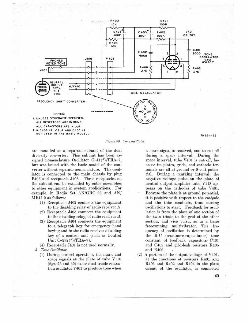
__ ----r----R 40 3 10K
JI06
R404 -:- 10K
P405
~~==~==--------to-~-A-~--+~~--~' u-----------+<>-I-- B --1-- -.e-+----.J
I
C403* .0IUF
C402 6000
R406 27K
R401 lOOK
V401 6SL7GT
C401
6000 TONE OSCILLA TO/\
. V401
R405 27K
6SL7GT
.----------------+<>-I--H-4--+.~-------------~~--6---~+_--~ I
,_-'--..... NEUTRAL OUTPUT
AMPL VI18 6Y6G
- ...... -+0-1-- J -+-;~+----'--------------J 6.3VAC I - ...... ---H~- I -~--~~~-~----------------.J
F'REQUENCY SHIF'T CONVERTER·
NOTES:
I. UNLESS OTHERWISE S·PECIF'IED,
ALL RESISTORS ARE IN OHMS,
ALL CAPACITORS ARE IN UUF.
2.* C403 IS .02UF ANO C405 IS NOT USEO IN THE BASIC MOOEL.
I I I
TONE OSCILLATOR
TM261-35
Figure 30. Tone oscillator.
are mounted as a separate subunit of the dual diversity converter. This subunit has been assigned nomenclature Oscillator 0-41 (*)JTRA-7, but was issued with the basic model of the converter without separate nomenclature. The oscillatoris connected to the .main chassis by plug P405 and receptacle Jl()6. Three receptacles on the subunit can be' extended by cable assemblies to other equipment in system applications. For example, in Radio Set ANJGRC-26 and ANJ MRO-2 as follows:
(1) Receptacle J402 connects the equipment to the disabling relay of radio receiver A.
(2) Receptacle J403. connects the equipment to the disabling relay, ofradio receiver B.
(3) Receptacle J404 connects the equipment to a telegraph key for emergency hand keying and to the radio receiver disabling key of a control unit (such as Control Unit 0-292(*)JTRA-7).
(4) Receptacle J401 is not used normally. b. Tone Oscillator.
(1) During normal operation, the mark and space signals at the plate of tube V11S (figs. 23 and 30) cause dUI1I-triode rehixation oscillator V401to produce tone when
a mark signal is received, and to cut off during a space interval. During the space interval, tube V401 is cut off, because its plates, grids, and cathode terminals are all at ground or O-volt potential. During a m.arking interval, the negative voltage pulse on the plate of neutral output amplifier tube V1l8 appears on the cathodes of tube V401. Because the plate is at ground potential, it is positive with respect to the catqode and the tube conducts, thus. causing oscillations to start. Feedback f{)r oscillation is from the plate of one section of the twin triode to the grid' of the other section. and vice versa, as in a basic free-running multivibrator. The frequency of oscillation is determined by the R-O (resistance-capacitance) time constant of feedback capacitors' 0401 and 0402 and grid-leak resistors R405 and R406.
(2) A portion of the output voltage of V401, at the junctions of resistors R401 and R403 and R402 and R404 in the plate circuit of the oscillator, is connected
43
"""'''OL' ~-----------------'--nl IF I --,----------------------------~-/
through terminals A and B of P405 and JI06 to PHONES KEYED TONE jack JI05. Oapacitor 0403 (0403 and 0405 in the A model), which is bridged across the monitoring leads, bypasses the higher harmonics of the relatively square-wave output of relaxation oscillator V401 to produce a more nearly sine-wave voltage in thc monitoring headphones.
c. Emergency Hand Keying.
44
(1) For emergency hand keying, OUTPUT switch SI02 of the converter unit (fig. 31) must be set to the SPAOE position (contacts 4 and 5 together). This position of switch S102 connects the grid (pin 1) of tube VIll to the junction point of resistors RI26 and RI28,which are ,connected in series between ground and the regulated -150-volt supply. The negative voltage across resistor RI26 cuts off tube VIlI which, in turn, cuts off tube VII3, causing a space signal to be transmitted over the d-c loops. As shown in figures 31, 71, and 72, the plate of tube VIl3 is connected through contacts 4 and 5 of switch Sl02 (bank B) to the contacts of a telegraph key. The plate circuit of carrier-control mark-hold tube VI05 is opened when the OUTPUT switch is in the SPAOE position. This prevents tube VI05 from establishing a steady mark on the d-c loops when the carrier is shut off.
(2) The operation of a telegraph key places ground on the plate pin of driver tube VII3 (if switch SI02 is in the SPAOE position), thus changing the plate potential from a positive value to a less positive value in approximately the same manner as though tube VII3 was changing from a nonconducting condition to a conducting condition in response to a received hlark signal. Accordingly, the operation of the telegraph key results in the keying of tbe polar and neutral out.:. put amplifiers. Polar space amplifier VIl6 conducts for the key-up condition; polar mark amplifier V115 conducts for the key-down condition. Neutral output amplifier VII8 conducts for the keydown condition and cuts off for -the
key-up condition. The polar loop can be used for frequency-shift hand keying (by connection to an exciter such as Frequency Shift Exciter 0-39(*)/TRA-7); the neutral loop can be used for c-\y hand keying in any application which requires an on-off current condition for keying.
39. Disabling of Radio Receivers (fig. 31).
a. Relay K401 and the disabling relays of the two radio receivers normally are not operated, In this state, the radio receivers are connected for reception. With one-way reversible operation, the service switch on the control unit is set at one way before operation is started. One end of the winding of relay K401 is connected to the regulated + 150-volt supply through current limiting resistor R409. The other end of the winding is connected through pins 0 and D of jack J404 and through the contacts of the service switch in the control unit to ground. Relay K401, therefore, will opcrate, and its contacts connect the disabling relays of thc two radio receivers to about 20 volts, developed across resistor R410 by the output of a small, full-wave, disk-type rcctifier, OR40I. The disabling relays in the radio receivers thus are operated to short-circuit the receiving antennas. This is necessary to protect the sensitive receiver circuits, since, in one-way operation, the same carrier frequency that is used for reception is used also for transmission to the distant radio receiving station.
b. Disk-type rectifier OR401 is connected to the 50- to 50-cycle secondary voltage of transformer T401, when the contacts of relay K401 are closed in the operated (energized) position. The a-c secondary supply is protected by fuse F401. The primary a-c voltage for transformer T401 is tapped off the normal 1I5-volt, 50- to 50-cycle supply to the converter unit at terminals 9 and 10 of terminal board E30I. This 1I5-volt supply is opened and closed by the contacts of the a-c supply switch of the converter unit. The lower contact (4) of relay K401 places ground on plate pin 8 of tube VI05, through the N contacts of P405 and J106, wh~n this relay is operated. This insures that a steady marking condition is established on the line to the operating shelter when the receiving circuits are cut off.
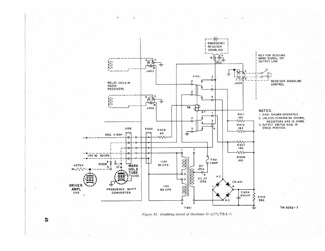
.... UI
f~!
(::~--------
~~~ I-----l \ ... ------- I
RELAY COILS IN RADIO RECEIVERS
I I I I I I' I I I I
J403
,:-------------~ -) ~
le, I )0 : \_ _ __ .J-----J I
t I t I I
--------------------~ JI06
J402 I
P405 R409 4K REG +150V _. _________________ .,.~_o_~-.D--~
K401
2 0
5
r--1111----, I EMERGENCY I I RECEIVER I
I DISABLING I L_-,. r-.J r---x A
B
3
~ I
~ 6T
-:-
=~~~~'.o~~i-:.-:.i : =~~!.:: ; i ' I-----~~ " ' II I --F--I
+275V 5102841 &.-.... : F401
'IAMP
..... ,,/\/\/'_.., _____ ~ oL., MARK i •• +--. .......... HOL D I
,'':'''''::_, l~·\ TUBE : ___ \ I ~- I '.-.- I ---. VIOS" I , ___ I --- , I
,_" ~ I DRIVE R ....... " ..,k-I .... _.... :
AMPL - I VIl3 FREQUENCY SHIFT I
CONVERTER : I I ___ ~ ___________________ J
115V 60 CPS
115V 60 CPS
AC
4 5
T401
Figure 31. Disabling circuit of Oscillator 0-41 (*)/TRA-7 .
I I I I I
KEY FOR SENDING MARK SIGNAL ON OUTPUT LINE
A ___ J_/o-_ I I
R411 160
R412 160
R408 160
0- - -1--o---1(-J ---""1----' RECEIVER
-:-
DISABLING : CONTROL
I I I I
NOTES: I. K401 SHOWN OPERATED. 2. UNLESS OTHERWISE SHOWN,
RESISTORS ARE IN OHMS. 3. OUTPUT SWITCH SI02 IN
SPACE POSITION.
R410 560
TM 5062-7
CHAPTER 4
FIELD MAINTENANCE INSTRUCTIONS
Note. This chapter contains information for field maintenance. The amount of repair that can be performed by units having field maintenance responsibility is limited only by the tools and test equipment available, and by the skill of the repairman.
Section I. TROUBLE SHOOTING AT FIELD MAINTENANCE LEVEL
lVarning: Certain precautions must be followed when measuring voltages above a few hundred volts. High voltages can cause a fatal, accident. 1Vhen it is necessary to measure high voltages, observe the following rules: First, connect the proper voltmeter lead to the circuit ground. Then place one hand in pocket. This will eliminate the possibility of making accidental contact with another part of the circuit, thus causing the electricity to travel from onc hand to the other through the body. If the voltage is less than 300 .volts, connect the remaining test lead to the hot terminal (which may be either positive or negative with respect to ground). If the voltage is greater than 300 Volts, shut off the power; then connect the hot lead, turn on the power, and note the reading on the voltmeter. Do not touch any part of the voltmeter, particularly when it is necessary to measure the voltage between two points both of which are at some potential with reRpect to ground. Before touching any part after the power is shut off, short the part to ground.
40. Trouble-shooting Procedures
The first step in trouble shooting a defective dual diversity converter is to sectionalize the fault. To sectionalize means to trace the fault to the major circuit responsible for the abnormal operation of the equipmelit. The second troubleshooting step is to localize the fault. To localize means to trace the fault to the. defective part responsible for the abnormal operation. Some faults, such as burned-out resistors, r-f arcing, and shorted transformers, often can be located by sight, smell, and hearing. The majority of troubles, however, must be located by checking voltage and resistance and then comparing the observed results with the voltage and resistance charts.
41. Test Equipment Required for Trouble Shooting
The test equipment require for trouble-shooting Dual Diversity Converter CV-31(*)/TRA-7 is listed below .. The technical manuals associated with the test equipment are listed also.
46
I Technical manual 1-------
Test equipment
Tube Tester I-177, or equaL ______ TM 11-2627. Electronic M ultimeter TS-505jU, T M 11-5511.
or equal. Signal Generator SG-I5/PCM, or TM 11-2096.
equal. Signal Generator I-72, or equaL ___
1 TM 11-307.
Oscilloscope OB-SA/U, or equaL __ 1 ~AVSHIPS 91, 272. Decibel Meter TS-399jU, or equaL _I TM 11-2045. Frequency Meter Set SCR-211-1· TM 11-300.
(*), or equal.
42. Visual Inspection a. Failure of the equipment to operate properly
usually will be caused by one or more of the following faults:
(1) Defective power cable. (2) Worn, broken, or disconnected cords or
plugs. (3) Burned-out fuse. (4) Wires broken because of excessive vibra
tion. (~) Loose or defective tubes.
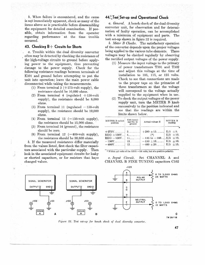
b. W'hen failure is encountered, and the cause is nqt immediately apparent, check as many of the items above as is practicable before disassembling the equipment for detailed examination. If possible, obtain information from the operator regarding performance 'at the time trouble occurred.
43. Checking B+ Circuits for Shorts a. Trouble within the dual diversity converter
, often may be detected by checking the resistance of the high-voltage circuits to ground before applying power to the equipment, thus preventing' damage to the power supply. Check for the following resistance readings between terminals of E301 and ground before attempting to put the unit into operation; leave the main power cable disconnected while taking the measurements.
(1) From terminal 3 (+275-volt supply), the resistance should be 10,000 ohms.
(2) From terminal 4 (regulated. + 150-volt supply), the resistance should be 8,000 ohms.
(3) From terminal 11 (regulated -150-volt supply), the resistance should be 19,000 ohms.
(4) From terminal 13 (-150-volt supply), the resistance should be 15,000 ohms ..
(5) From terminal 14 (ground), the resistance should be zero.
(6) From terminal 12 (-400-volt supply), the resistance should be 30,600 ohms.
b. If the measured resistances differ materially from the values listed, first check the filter capacitors associated with the particular supply. Then look in the associated'equipment circuits for leaky or shorted capacitors, or for resistors that have changed values. .
SIGNAL GENERATOR SIGNAL GENERATOR
OUTPUT GND OUTPUT GND
- -
JI02 ' JI02 JIOI
! ! ICHAANI
- -ICHBANI
A B
44.:Tes(Set-up and Operational Check
a. General. A bench check of the dual diversity converter unit, for observation and for determination of faulty operation, can be accomplished with a minimum of equipment and parts. The test set-up shown in figure 32 is required.
b. Meter B Ohecks. The satisfactory operation of the converter depends upon the proper voltages being applied to the various tube elements. These voltages may be checked regularly by observing the rectified output voltages of the power supply.
(1) ~feasure the input voltage to the primary of power transformersT301 and T302 and adjust this voltage at the time of installation to 105, 115, or 125 volts. Check to see that connections are made to the proper taps on the primaries of these transformers so that the voltage will correspond to the voltage actually supplied to the equipment when in use.,
(2) To check the output voltages of the power supply unit, turn the METER B knob successively to the position indicated and see that the readings are wi thin the limits shown below.
METER B switch' E301 termi-position nal No, to
ground Actual voltage E I MET~R B
I readmg ..
+280 ±15 _____ E/5 ±9. (*) I E/5 ± 10.
-145 to -160--I-E/5 ±10. -150 ±10 _____
1
E/5 ±10. -400 ±20 _____ E/5 ±15.
+275V _______ 3 _______ _ REG +150V __ 4 ________ , REG -150V __ 11. _____ .1 -150V _______ 13 ______ _ - 400V _ _ _ _ _ _ _ 12 ______ _
I * Within ±3 volts of the REG -150 volts, but of a positive polarity.
c. Input Oircuit. Set CHANNEL A and CHANNEL B FINE TUNING capacitors C102
JI03
A
- B
C 0
D
E
-
POLAR OUTPUT
NEUTRAL OUTPUT
o TO 3,000 OHMS 25 WATTS
o TO 1,000 OHMS 10 .wATTS
Figure 32. Test set-up for bench check of dual diversity converter.
47
:and 0104 at their midpositions. T elocations of :screw driver controls 0101, 0105, 0103, and 0106 involved in the procedures which fo ow are shown in figures 4 and 5.
•
48
(1) Oonnect the signal genera or to OHAN A receptacle J101 of the onverter and set the signal generator f equency to a value corresponding to t at of the i-I input from the radio rec ivers (470 kc for Radio Receiver R-1 2(*)jMRO-2 and 500 kc for Radio Re eiver R-388j URR). Set the input at 1 volt. This voltage requirement is ba d on the use of a signal generator of 10 -ohm output impedence. Do not conlie t an input to OHAN B receptacle J102 while making tests on channel A.
(2) Oonnect a VTVM (vacuu tube voltmeter) from terminal 3 of etwork ZlO3 to ground and adjust the tor to OlOl with a screw mum indication on the to 22 volts).
uning capaciiver for maxioltmeter (13
(3) Oonnect the VTVM from terminal 2 of network Z104 to ground, nd check to see that the voltage at thi point is 1.75 to 3.5 volts throughout he complete range of tuning capacitor 0 05.
(4) Oonnect the VTVM from erminal 3 of BAND WIDTH switch Sl jlE to ground, or from terminal 4 of E1d3. Turn the BAND WIDTH knob td NARROW. Set the test oscillator output at .1 volt and adjust tuning capacitor OlO5 to give a maximum voltage indication (10 to 25 volts).
(5) Repeat step (4), but turn the BAND WIDTH knob to WIDE. Oheck to determine that the voltage indication is between 20 and 40 volts. .
(6) Oonnect the signal generator to OHAN B receptacle J102 of the converter and set the signal. frequency to a value corresponding to that of the i-f input from the radio receiver. Set the signal generator output at 1 volt. Do not connect an input to OHAN A receptacle JI01 while making tests on channel B.
(7) Oonnect a VTVM from terminal 3 of network Z101 to ground and adjust tuning capacitor 0103 for a maximum indication on the voltmeter (13 to 22 volts).
(8) Oonnect the VTVM from terminal 2 of
network Z102 to ground and check to see that the voltage at this point is 1:7.5 to 3.5 volts throughout the complete range oftuning capacitor 0106. .
(9) Oonnect the VTVM from terminal 3 of BAND WIDTH switch S10lE to ground. Turn the BAND WIDTH knob to NARROW. Set the test oscillator output at .1 volt and adjust tuning capacitor 0106 to give a maximum voltage indication . (8 to 25 volts).
(lO) Repeat step (9), but turn the BAND WIDTH knob to WIDE. Oheck to see that the voltage indication is between 15 and 40 volts.
d. Limiter Circuit . . After alining and checking the input circuit according to the prOcedures above, check the limiter circuit in accordance with the following:
(1) Oonnect the signal generator to channel A and adjust its frequency to the i. f. of the receiver normally used in conjunction with this equipment. Do not con~ connect any input to channel B. Turn the BAND WIDTH knob to WIDE and the METER B knob to INPUT. Adjust the signal generator output level to give a meter indication of +50.
(2) See that the input voltage to the limiter, as' measured by the VTVM, from terminal 3 of BAND WIDTH switch S10lE (or from terminal 4 of V103) to ground, is ilOt greater than 6 volts.
(3) Oonnect the VTVM from terminal 4 of tube V108 (or from terminal 42 of mounting strip EI03), to ground, and check to see that the voltage is 6 ± 2 volts.
(4) Set the output level of the test. oscillator at .5 mv (millivolts). If the VTVM indicates at least 4 volts, raise the output level of the test oscillator to 500 mv and check to see that the VTVM indicates between 4 and 8 volts.
(5) Oonnect an oscilloscope from terminal 4 of tube V108 (or from terminal 42 of mounting strip E103) to ground. Use a saw-tooth sweep frequency suitable to obtain a 3-cycle pattern. Obs'erve that the . waveform of the 50-kc signal is approximately as shown in A of figure 33.
(6) Transfer the signal generator from channel A input to channel B input. Do not connect any input to channel A. Repeat
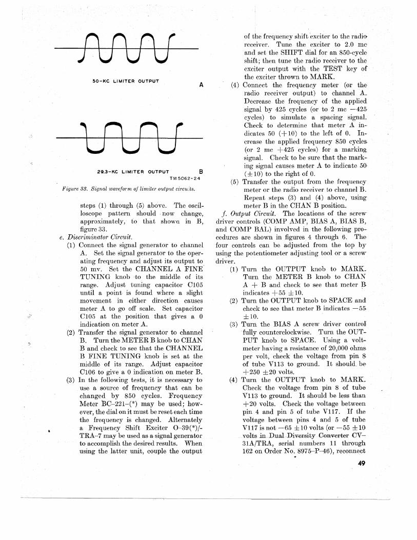
JUUU SO-KC LIMITER OUTPUT
A
,nn r 29.3-KC LIMITER OUTPUT B
TM5062-24
Figure 33. Signal waveform of limiter output circuits.
steps (1) through (5) above. The oscilloscope pattern should, now change, approximately, to that shown in B, figure 33.
e. Discriminator Oircuit. (1) Oonnect the signal generator to channel
A. Set the signal generator to the operating frequency and adjust its output to 50 mv. Set the OHANNEL A FINE' TUNING knob to the middle of its range. Adjust tuning capacitor 0105 until a point is found where a slight movement in either direction causes meter A to go off scale. Set capacitor 0105 at the position that gives a 0 indication on meter A.
(2) Transfer the signal generator to channel B. Turn the METER B knob to OHAN B and check to see that the OHANNEL B FINE TUNING knob is set at the middle of its range. Adjust capacitor 0106 to give a 0 indication on meter B.
(3) In the following tests, it is necessary to use a source of frequency that can be changed by 850 cycles. Frequency Meter BO-221-(*) may be used; however, the dial on it must be reset each time the frequency is changed. Alternately a Frequency Shift Exciter 0-39(*)/TRA-7 may be used as a signal generator to accomplish the desired results. When using the latter unit, couple the output
of the frequency shift 'exciter to the radio receiver. Tune the exciter to 2.0 me and set the SHIFT dial for an 850-cycle shi~t; then tune the radio receiver to the exciter output with the TEST key of the exciter thrown to MARK.
(4) Oonnect the frequency meter (or the, radio receiver output) to channel A. Decrease the frequency of the applied signal by 425 cycles (or to 2 mc -425· cycles) to simulate a spacing signaL Oheck to determine that meter A indicates 50 (+ 10) to the left of o. Increase the applied frequency 850 cycles. (or 2 mc +425 cycles) for a marking signaL Oheck to be sure that the marking signal causes meter A to indicate 50. (± 10) to the right of O.
(5) Transfer the output from the frequency meter or the radio receiver to channel B. Repeat steps (3) and (4) above, using meter B in the OHAN B position.
f. Output Oircuit. The locations of the screw driver controls (OOMP AMP, BIAS A, BIAS B, and OOMP BAL) involved in the following procedures are shown in figures 4 through 6. The four controls can be adjusted from the top by usiJ?g the potentiometer adjusting tool or a screw driver.
(1) Turn the OUTPUT knob to MARK. Turn the METER B knob to OHAN A + B and check to see that meter !3-indicates +55 ±10.
(2) Turn the OUTPUT knob to SPAOE and check to see that meter B indicates -55-±1O.
(3) Turn the BIAS A screw driver control 'fully counterclockwise. Turn the OUTPUT knob to SPAOE. Using a voltmeter having a resistance of 20,000 ohms. per volt, check the voltage from pin 8 of tube VIl3 to ground. It should. be + 250 ± 20 volts.
(4) Turn the OUTPUT knob to MARK. Oheck the voltage from pin 8 of tube VIl3 to ground. It should be less than +20 volts. Oheck the v{)ltage between pin 4 and pin 5 of tube V117. If the voltage between 'pins 4 and 5 of tube VIl7 is not -65 ± 10 volts (or -55 ± 10 volts in,. Dual Div.ersity Gon:v:er-ter OV-31A/TRA, serial numbers 11 through 162 on Order No. 8975-P-46), reconnect .
49
the lead from pin 4 of tube V117 (which is also connected to pin 5 of tube V116) to the junction of the two resistors (RI62 through RI67) that provides a voltage nearest to -65 volts (or -55 volts in the aforementioned model numbers).
(5) Remove tube VI05 from its socket aud check the voltage from pin 8 of tube V117 to ground. It should be + 185 ± 20 volts. Next, turn the OUTPUT knob to SPACE and check to see that the voltage changes to -145 ± 10 volts. Replace tube VI05 in its socket.
(6) Check to determine that the operation of the OUTPUT switch to MARK and to SPACE results in keying the polar and neiltralloop circuits. To do this, attach two rheostats to JI03, as shown in C, figure 32. These rheostats simulate the output loops, so that the dual diversity converter may be tested under simulated operating conditions.
(a) With the METER B knob at POLAR, determine that the POLAR OUTPUT MARK and SPACE potentiometers can be adjusted to produce loop currents as follows:
Simulated loop resistance in ohms between terminals A Meter iudication in rna' and B of jack n03
0___________________ Less than ±20: 2,000 approximately ____ More than ±25.
'Deflection to the right for MARK and deflection to the Jeft for SP AOE. .
(b) Turn the METER B switch to NEUTRAL. With the rheostat across pins D and E of jack J103 adjusted as in thc chart below, determine that the NEUTRAL OUTPUT potentiometer can be adjusted to ·produce neutral currents as follows:
Simulated loop resistance in Ii
ohms between terminals D Meter indication in rna and E of jack J103
------------------------------0____ _ _ _ _ _ _ _ ____ _ _ _ __ _ Less than +40. 800.-------- __________ More than +60.
g. Drift Compensator Circuit. To test this circuit, set the controls and make the adjustments as follows:
50
(1) Turn the OUTPUT knob to NORMAL, and the AMp GAIN knob fully co uri ter-
clockwise. Operate the DRIFT COMPENSATOR switch to IN. Turn the LIMITER knob fully clockwise. Turn the COMP AMP screw driver control fully counterclockwise. Turn the METER B switch to CHAN A + B; then check to see that meter B indicates O± 5 volts.
(2) Turn the METER B switch to POLAR, and adjust the BIAS A screw driver control to the two positions where a slight movement of the control changes the loop condition from a mark to a space, and from a space to a mark. Leave the BIAS A control midway between the two positions.
(3) Turn Meter B switch to CHAN A + B. Turn the COMP AMP screw driver control in a clockwise direction until the meter B reading is increased by 5 to the right or to the left, depending on whether the indication in step (1) above is to the right or to the left. Adjust the BIAS B screw driver control to a position where, with a slight movement of the control, the meter B reading just mentioned changes back and forth between positive and negative readings.
(4) Set the COMP AMP screw driver control at its midposition. Turn the AMP GAIN control clockwise until the d-c loop currents can be changed from a mark to a space by the CHANNEL A (or B) FINE TUNING knob, when an i-f input is connected to the CHAN A (or CHAN B) receptacle (JIOI or JI02).
(5) Adjust the screw driver controls COMP BAL and COMP AMP until meter B indicates + 70 ± 5 for a mark (OUTPUT switch at MARK) and -70 ± 5 for a space (OUTPUT switch at SPACE) These readings should be steady. Wait
. several seconds, if necessary, to obtain steady meter indications. Slowly turn the LIMITER knob counterclockwise until the meter reading of + 70 for a mark is reduced to +50 and, at the same time, the meter reading of -70 for a space reduces to a value between -40 and -60. Turn the LIMITER knob, fully clockwise; then turn the knob slowly counterclockwise until the meter indication is just on the verge of being de-
creased. Leave the LIMITER knob at this setting.
h. Tone Oscillator Circuit: Turn the OUTPUT knob to MARK. Connect a headphone to the PHONES KEYED TONE jack, J105, and make sure that there is a tone output. Turn the output knob to SPACE and check to see that there is no tone output.
input from the radio rec.eiver is reduced to zero. Connect the i-f output from the radio receiver to channel B and adjust the i-f input from the radio receiver to channel B to give an indication of 50 on meter B. Check to see that the output circuit just remains spacing. Reduce the input from tIre radio receiver to zero and make sure that the output restores to marking.
i. Mark-Hold Circuit. In testing this circuit, a freqUency shift exciter and a radio receiver may be used as a source of frequency shift signals. Connect the i-f output from the receiver to channel A and operate the DRIFT COMPENSATOR switch to OUT and the OUTPUT switch to REVERSE. Tune the frequency shift exciter to 2.0 mc and set the SHIFT dial for an 850-cycle shift. Then tune the radio receiver to the exciter output with the TEST key of the exciter thrown to MARK. Turn the METER B switch to INPUT and adjust the input to the converter to give an indication of 50 on meter B. Adjust the MARK-HOLD LEVEL knob until the output circuit just remains spacing. Check to determine that the output restores to marking when the
45. Trouble-Shooting Chart
Symptom
1. White pilot fails to light when AC 8UPPLY switch is turned to ON.
2. Red pilot Jails to light when PLATE switch is turned to ON.
3. All voltages too high or too low.
4. +275V does not read in range of +47 to +65 on meter B.
5. REG + 150V does not read +20 to +40 on meter B.
6: REG -150V indication not -20 to -40 on meter B.
7. -150V indication not -20to -40 on meter B.
8. -400V indication not -65 to -95 on meter B.
9. Meter B on INPUT fails to give an indication.
When the indicated results are not obtained during one or more of the operational checks described in the preceding paragraph, consult the trouble-shooting chart below. Connect a signal generator to JIOI orJ102 as shown in A or B, figure 32. Also, make the connections to JI03 with rheostats as shown in C, figure 32. These rheostats simulate the output loops so that the dual diversity converter may be tested under simulated operating conditions. The signal generator should be set to the frequency normally fed. to input jacks JIOI and JI02 by the radio receivers used with the converter in actual operation.
Probable trouble
1. A-c line, safety switches 8301 and 8302, transformer T302, fuses F301 and F302, AC 8UPPL Y switch 8303, receptacle J104, pilot lamp 1301, or filter Z112.
2. Pilot lamp 1302, transformer T301, or plate· switch 8304.
3. Meter B, or tap connections on transformers T301 and T302.
4. T301 winding 5-6-7, choke L301, T302 winding 8-9, capacitors C301 and C302, or tube V301.
5. Tubes V304 or V305, capacitors C307 or C308, T301 winding 11-12, T302 winding 5-7, or resistors R308 to R321.
6. Tubes V303 or V306, capac~tors C305 or C306, T302 winding 12-13, or resistors R301 to R306.
7. Tube V302, resistor R307, T301 winding 8-9-10, capacitors C303 or C304, choke L302, or T302 winding 6-7.
8. Circuit wiring. V303, R301, R302, C305, C306, T302 winding 12-13, T301 winding 6-7.
9. Tubes Vl04 (section 3-4-5), V103, or VIOl and V102, or associated circuit elements.
Corrections
1. Check wiring and repair or replace defective apparatus. .
2. Check wiring and repair or replace defective apparatus.
3. Check and replace defective apparatus.
4. Check and replace defective apparatus.
5. Check and replace defective apparl1.tus.
6. Check and replace defective apparatus.
7. Check and replace defective apparatus.
8. Check continuity.
9. Check wiring and repair or replace defective apparatus.
51
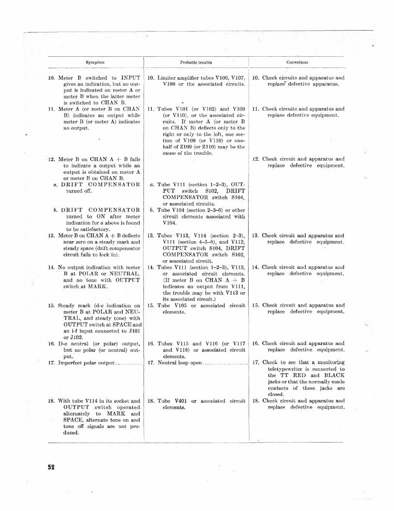
Symptom I Probable trouble Corrections
:'-~et: B switched to INPUT-II- 10. Limiter amplifier tubes V106, V107, - -:~~-e-Ck- cir~u-it-s-a-n-~~-p-pa-ratu~ an:
gives an indication, but no out- V108 or the associated circuits. replace" defective apparatus. put is indicated on meter A or meter B when the latter meter is switched to CHAN B.
11. Meter A (or meter B on CHAN B) indicates an output while meter B (or meter A) indicates no output.
-12. Meter B on CHAN A + B fails to indicate a output while an output is obtained on meter A or meter B on CHAN B.
(t. DRIFT COMPENSATOR turned off.
b. DRIFT COMPENSATOR turned to ON after meter indication for a above is found to be satisfactory.
13. Meter B on CHAN A + B deflects near zero on a steady mark and steady space (drift compensator circuit fails to lock in).
14. No output indication with meter B at POLAR or NEUTRAL, and no tone with OUTPUT switch at MARK.
15. Steady mark (d-c indication on meter B at POLAR aDd NEUTRAL, and steady tone) with OUTPUT switch at SPACE and an i-f input connected to J101 or J102.
16. D-c neutral (or polar) output, but no polar (or neutral) output.
17. Imperfect polar output. ________ _
11. Tubes VIOl (or VI02) and VI09 (or VllO), or the associated circuits. If meter A (or meter B OIl CHAN B) deflects only to the right or only to the left, one section of VI09 (or VllO) or onehalf of Z109 (or ZllO) may be the cause of the trouble.
a. Tube Vl11 (section 1-2-3), OUTPUT switch S102, DRIFT COMPENSATOR switch S104, or associated circuits.
b. Tube V104 (section 2-3-6) or other circuit elements associated with V104.
13. Tubes V1l3, V1l4 (section 2-3), Vlll (section 4-5-6), and V1l2, OUTPUT switch S104, DRIFT COMPENSATOR switch S102, or associated circuit.
14. Tubes Vll1 (section 1-2--3), V113, or associated circuit elements. (If meter B on CHAN A + B indicates an output from Vll1, the trouble may be withV113 or its associated circuit.)
15. Tube VI05 or associated circuit elements.
16. Tubes V115 and V116 (or V117 and V118) or associated circuit elements.
17. Neutral loop open ________________ _
18. With tube V114 in its socket and 18. Tube V401 or associated circuit OUTPUT switch operated elements. alternately to MARK and SPACE, alternate tone on and tone off signals are not pro-duced.
-------- --------- ---
52
11. Check circuits and apparatus and replace defective equipment.
12. Check circuit and apparatus and replace defective equipment.
13. Check circuit and apparatus and replace defective equipment __
14. Check circuit and apparatus and replace defective equipment.
15. Check circuit and apparatus and replace defective equipment.
16. Check circuit arid apparatus and replace defective equipment.
17. Check to see that a monitoring teletypewriter is connected to the TT RED and BLACK jacks or that the normally made contacts of these jacks are closed.
18. Check circuit and apparatus and replace defective equipment.
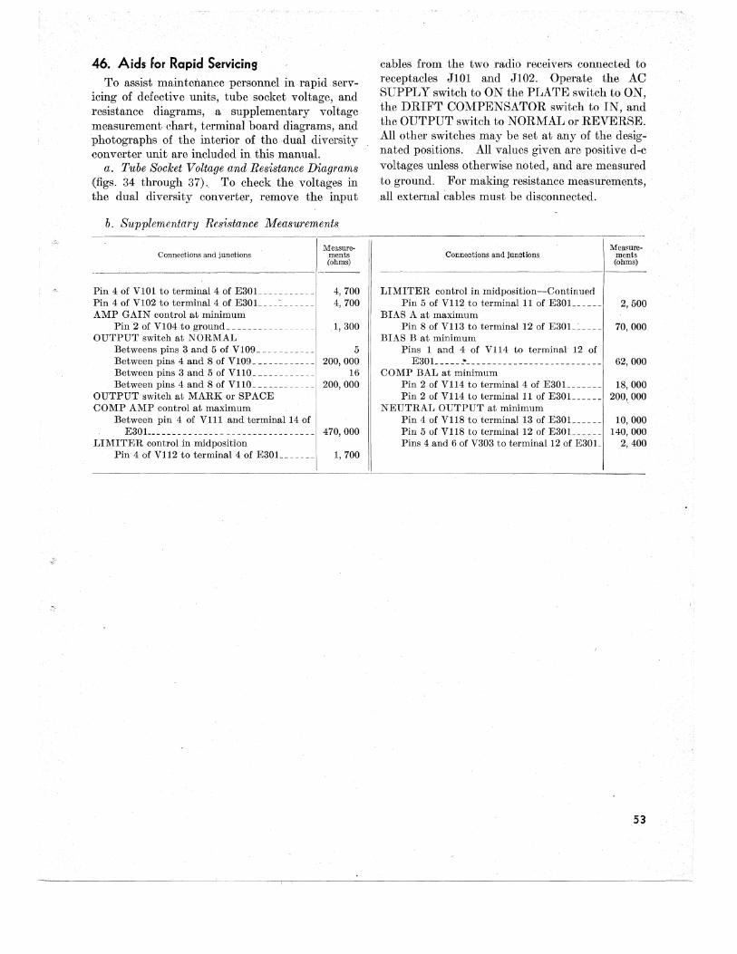
46. Aids for Rapid Servicing To assist maintenance personnel in rapid serv
icing of defective units, tube socket voltage, and resistance diagrams, a supplementary voltage measurement chart, terminal board diagrams, and photographs of the interior of the dual diversity ~onverter unit are included in this manual.
a. Tube Socket Voltage and Resistance Diagrams (figs. 34 through 37).. To check the voltages in the dual diversity converter, remove the input
b. Supplementary Resistance Measurements
Connections and jnnctions
Pin 4 of VIOl to terminal 4 of E30L ______ .. __ _ Pin 4 of VI02 to terminal 4 of E30L ___ ~ _____ _ AMP GAIN control at minimum
Pin 2 of VI 04 to ground _ _ _ _ _ _ _ _ _ _ OUTPUT switch at NORMAL
Measurements (ohms)
4, 700 4, 700
1, 300
Betweens pins 3 and 5 of VI09 _ _ _ _ _ _ _ _ _ _ _ 5 Between pins 4 and 8 of VI09 ____________ 200,000 Between pins 3 and 5 of V 11 0 _ _ _ _ _ _ _ _ _ _ _ _ 16 Between pins 4 and 8 of VllO ____ . ________ 200,000
OUTPUT switch at MARK or SPACE COMP AMP control at maximum
Between pin 4 of V111 and terminal 14 of E30L _ _ _ _ _ _ _ _ _ _ _ _ _ _ _ _ _ _ _ _ _ _ _ _ _ _ _ _ _ _ 470, 000
LIMITER control in mid position Pin 4 of V112 to terminal 4 of E30L ______ , 1, 700
I
cables from the two radio receivers connected to receptacles JIOI and JI02. Operate the AC SUPPLY switch to ON the PLATE switch to O~, the DRIFT COMPENSATOR switch to IN, and the OUTPUT switch to NORMAL or REVERSE. All other switches may be set at any of the designated positions. All values given are positive d-c voltages unless otherwise noted, and are measured to ground. For making resistance measurements, all external cables must be disconnected.
Connections and junctions Meamre
mcnts (ohms)
LIMITER contra.l in midposition-Continued I Pin 5 of V112 to terminal 11 of E30L_ _ _ _ _ 2,500
BIAS A at maximum Pin 8 of V 113 to terminal 12 of E30L _ _ _ _ _ 70, 000
BIAS B at minimum Pins 1 and 4 of V114 to terminal 12 of
E30L ____ ~._ _ _ _ _ _ _ _ _ _ _ _ _ _ _ _ _ _ _ _ _ _ _ _ _ _ 62,000
COMP BAL at minimum Pin 2 of V114 to terminal 4 of E30L______ 18,000 Pin 2 of V114 to terminal 11 of E30 L _ _ _ _ _ 200, 000
NEUTRAL OUTPUT at minimum Pin 4 of V118 to tcrminalI3 of E30L_____ 10,000 Pin 5 of V118 to terminal 12 of E30L _____ 140,000 Pins 4 and 6 of V303 to terminal 12 of E30L 2,400
53
---,--, ------------------------ .-------~-
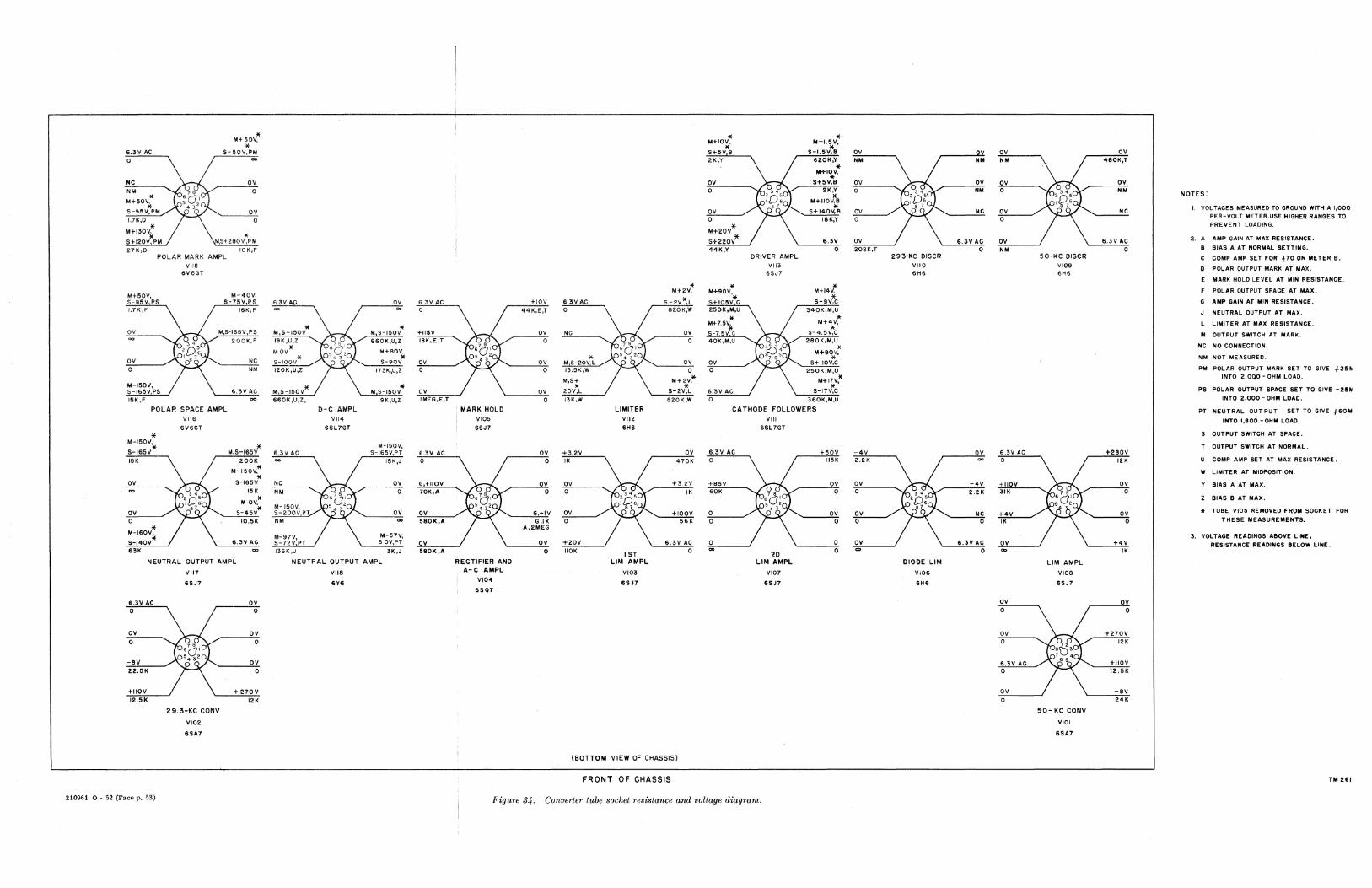
6.3V AC o
NC NM
* M+SOVif
S-95V,PM 1.7K,D
* M+130V,
* S+IZOV,PM 27K,D
* M+ SOY,
* S-1l0V,PM
OV o
OV o
* ,St280V,~M
10K,F POLAR MARK AMPL
VI15
MtSOV, S-95V PS
OV
OV o
15K,F
6V6GT
M-40V, S-75V,PS
16K,F
M,S-165V,PS 200K,F
NC NM
6.3V AC
POLAR SPACE AMPL
vile
* M-150V\I
S-165V 15K
OV
OV o
* M-160V,
S-140V* 63K
6V6GT
* M,S-16SV 200K
M-150V,*
* S-165V 15K
M OV,*
S-45V* 10.5K
8.3V AC
NEUTRAL OUTPUT AMPL
VI17
6.3V AC o
OV
o
-8V 22.5K
+IIOV 12./lK
210061 0 - 52 (Face p. 53)
6SJ7
29.3-KC CONY
VI02
6SA7
OV o
OV o
OV o
+270V 12K
6.3V AC
* M,S-IIlOV 19K,U,Z
MOV*
S-IOOV* 120K,U,Z
M,S-150V* 6S0K,U,Z,
6.3V AC
Ne NM
M-150V, S-200V,PT NM
M-97V, S-72V PT 136K,J
D-C AMPL
VII4 6SL7GT
r--__ O"".:;~ ~.3VAC tlOV 6.3V AC o 44K,E,T
* M S -150 V -;+",",,"OC:.:V:-:,..-, 660K,U,Z 18K ,E,T
OV NC o
Mt80V,
* S-90V ...,O;.:v'--__ .r 173K ,Ul Z 0
OV o
* M S-20V L 13.SK,W
M-150V, S-16SV,PT
15K,J
OV o
OV
M-57V, SOV,PT
3K,J
MARK HOLD
VI05 6SJ7
OV o
M,S+
* 20V,L 13K,W
6.3 V AC OV -;+-;;3",.2 ... V,-_-.. o 0 IK
G tllOV OV ~V,-__ ........ 70K,A 0 0
OV G,-IV OV 580K,A G,tK -:0:-:---'
A,2MEG
OV OV +20V 580K,A 0 -;I~IO~K~--J
LIMITER
VII2
6H6
* M+2V,
S-2V*,L 820K,W
OV o
OV o
M+2V;*
* S-2V,L 820K,W
OV 470K
+3.2V IK
6.3V AC o
NEUTRAL OUTPUT AMPL RECTIFIER AND 1ST
LIM AMPL
VII8
6Y6
A-C AMPL
VI04
6SQ7
VI03
6SJ7
(BOTTOM VIEW OF CHASSIS)
FRONT OF CHASSIS
* M+IOV, * M+I.~V,
* S+5V B 2K,Y
5-1.11 V,8 .,;:O",V"-__ """,, 620K,Y NM
* M+I~V,
S+IlV,B ~O:-:V ___ ........ 2K,Y 0
OV o
OV o
* M+20V
* S+220V 44K,Y
DRIVER AMPL Vll3
SSJ7
* M+IIOV,B
* S+140V,B IBK,Y
6.3V o
* M+14V,
* S-9V,C 340K,M,U
* M+4V,
* S-4.5V,C 280K,M,U
* M+9OJ' ov S+IIOV,C o 2S0K,M,U
M+17V~ * 6.3V AC S-17V,C
o 360K,M,U
CATHODE FOLLOWERS
VIII 6SL7GT
6.3V AC o
+8SV SOK
o o
o co
20 LIM AMPL
VI07
6SJ7
+50V IISK
OV o
OV o
o o
OV o
OV 202K,T
-4V 2.2K
OV o
OV o
OV
29:3-KC DISCR
VIIO 6H6
DIODE LIM
V,06
6H6
Figure 34. COr/verter tube socket resistance and voltage diagram.
NM
OV NM
NC
6.3V AC o
OV
-4V 2.2K
NC o
6.3V AC o
6.3V AC o
+IIOV 31K
+4V IK
OV ...
OV o
OV o
6.3V AC o
OV o
50-KC DlSCR
VI09 SHS
LIM AMPL
VIOS
6SJ7
50-KC CONV
VIOl
6SA7
OV 480K,T
OV NM
NC
6.3V AC o
+280V 12K
OV o
OV o
+4V IK
OV o
+270V 12K
+IIOV 12.5K
-8V 24K
NOTES:
VOLTAGES MEASURED TO GROUND WITH A 1,000 PER-VOLT METER.USE HIGHER RANGES TO PREVENT LOADING.
2. A AMP GAIN AT MAX RESISTANCE.
B BIAS A AT NORMAL SETTING.
C COMP AMP SET FOR f10 ON METER B.
o POLAR OUTPUT MARK AT MAX.
E MARK HOLD LEVEL AT MIN RESISTANCE.
F POLAR OUTPUT SPACE AT MAX.
G AMP GAIN AT MIN RESISTANCE.
NEUTRAL OUTPUT AT MAX.
L LIMITER AT MAX RESISTANCE.
M OUTPUT SWITCH AT MARK.
NC NO CONNECTION.
NM NOT MEASURED.
PM POLAR OUTPUT MARK SET TO GIVE +25~ INTO 2,OQO - OHM LOAD.
PS POLAR OUTPUT SPACE SET TO GIVE -25W INTO 2,000 - OHM LOAD.
PT NEUTRAL OUTPUT SET TO GIVE .j.60M
INTO 1,900 - OHM LOAD.
S OUTPUT SWITCH AT SPACE.
T OUTPUT SWITCH AT NORMAL.
U COMP AMP SET AT MAX RESISTANCE.
W LIMITER AT MIDPOSITION.
Y BIAS A AT MAX.
Z BIAS 8 AT MAX.
* TUBE VI05 REMOVED FROM SOCKET FOR ··-"!'1ieSE·ftASUREMENTS.
3. VOLTAGE READINGS ABOVE LINE, RESISTANCE READINGS BELOW LINE.
TM 261
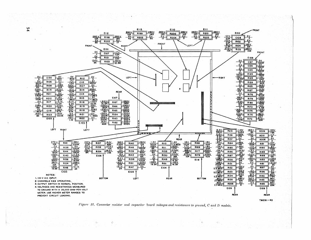
VI .too.
EI03 t LEFT Rlr LEFT
EI05 NOTES:
1 •. 1I5·V A·C INPUT. 2. CHANNELS' A&B OPERATING. 3. OUTPUT SWITCH IN NORMAL ·POSITION.
4. VOLTAGES AND RESISTANCES MEASURED TO GROUND WITH A 20,OOOOHM-PER-VOLT METER. USE HIGHER METER RANGES TO
PREVENT CIRCUIT LOADING.
EI06
EI09 f REAR
Figure .35. Converter resistor and capacitor board voltages and resistances to ground, C and D models,.
{-
FRONT
FRONT
REAR
TM261- 40
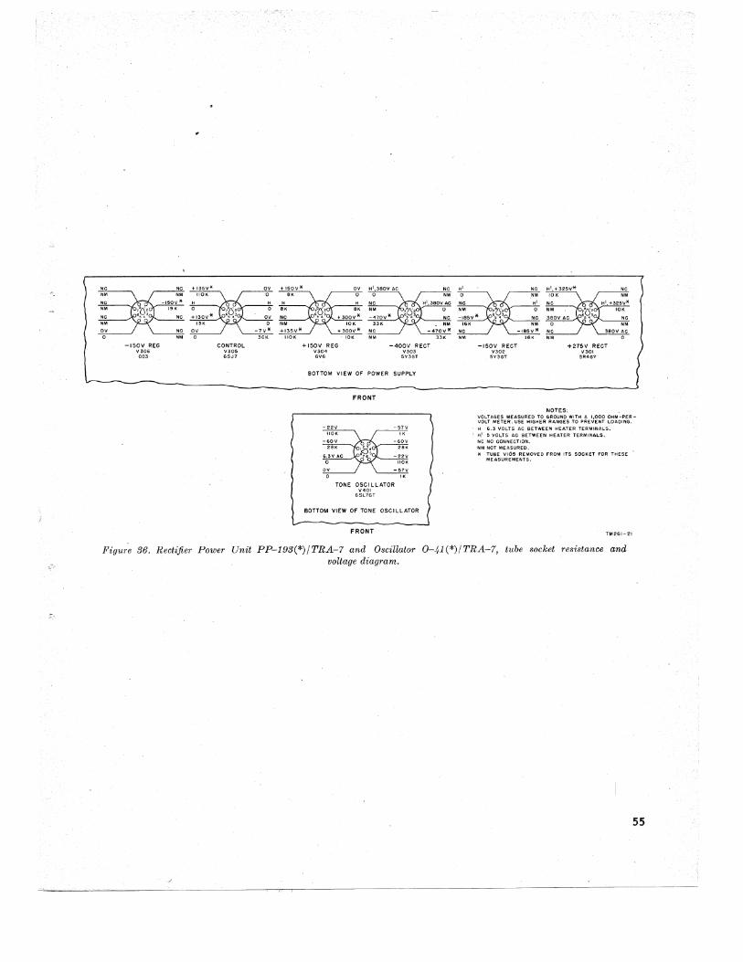
-ISOV REG V306 003
CONTROL V30S 6SJ7
+ 150V REG V304 6Y6
-400V RECT V303
SY3GT
BOTTOM VIEW OF POWER SUPPLY
FRONT
TONE OSCILLATOR V401
6SL7GT
BOTTOM VIEW OF TONE OSCILLATOR
FRONT
-ISOV RECT V302
SY3GT
+27SV RECT V301 ~R4G'i'
NOTES; VOLTAGES MEASURED TO GROUND WITH A I,DOOOHM-PERVOLT METER. USE HIGHER RANGES TO PREVENT lOADING. H 6.3 VOLTS AC BETWEEN HEATER TERMINAL:S .
• Hil ~ VOLTS AC BETWEEN HEATER TERMINALS. Ne: NO CONNECTION. NM NOT MEASURED. ~ TueE v.OS REMOVED "FROM ITS SOCKET FOR THESE
MEASUREMENTS.
TM261-21
Figure 36. Rectifier Power Unit PP-193(*)JTRA-7 and Oscillator 0-41 (*)JTRA-7, tube socket resistance and voltage diagram.
55
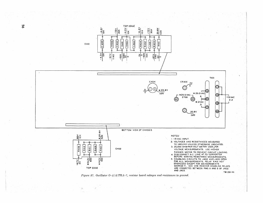
U1 0- fOP EDGE:
> > > "- > ~:£ > ~ co
'" :£ :£ .t '" 0 0 ~Q .... 0 ';" I"J I I"J >2 '"
r. E401
C404
~8V o . 520
BOTTOM VIEW OF CHASSIS
E402
TOP EDGE
NOTES:
CR401 OV
0f0
~8V 520
I. 115 VAC INPUT.
T401
2. VOLTAGES AND RESISTANCES MEASURED TO GROUND UNLESS OTHERWISE INDICATE,!).
115VAC 2.2
3. 20,000 OHM-PER-VOLT METER USED ,FOR VOLTAGE MEASUREMENTS. USE HIGHER
RANGES METER TO PREVENT CIRCUIT LOADING. 4. DISCONNECT A-C LINE AT FS CONVERTER
BEFORE MAKING RESISTANCE MEASUREMENTS. 5. DISABLING CIRCUITS TO J402 AND J403 OPEN
FOR ALL MEASUREMENTS. RELAY K401 NOT ENERGIZED EXCEPT FOR MEASUREMENTS MARKED". 600 OHM RECEIVER DISABLING RELAYS ARE CONNECTED BETWEEN PINS A AND B OF J402 AND J403.
TM 261-41
Figure 37. Oscillator 0-41A/TRA-7, resistor board voltages and resistances to ground.
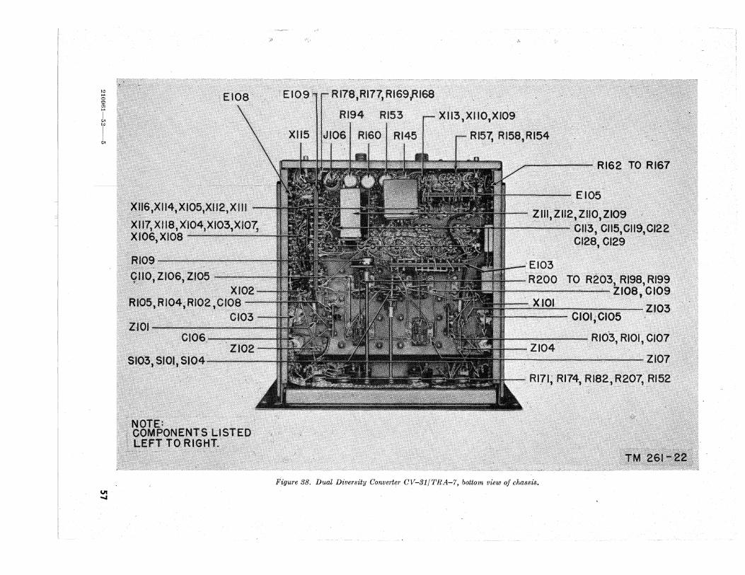
"" I-' o ~ ~ I-'
i '" r '"
UI ..... Figure 88. Dual D1:versity Converter CV-31/TRA-7, bottom view of chassis.
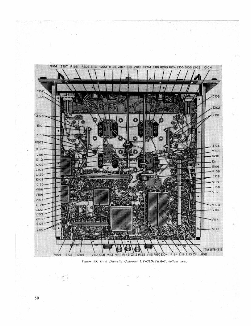
~-
Figure 39. Dual Diversit'y Converter CV-31l)(TRA-7, bottom view.
58
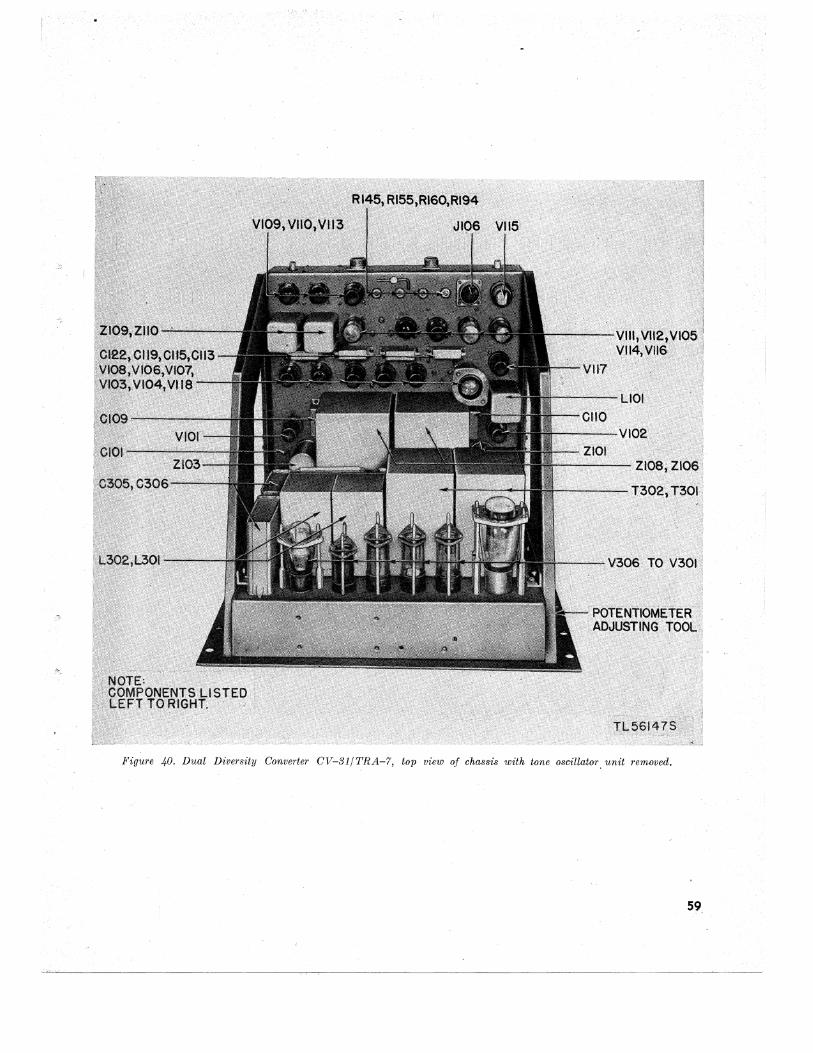
F'igllre 40. Dual Diversity Converter CV-31/TRA-7, top view of chassis with tone oscillator. unit removed.
59
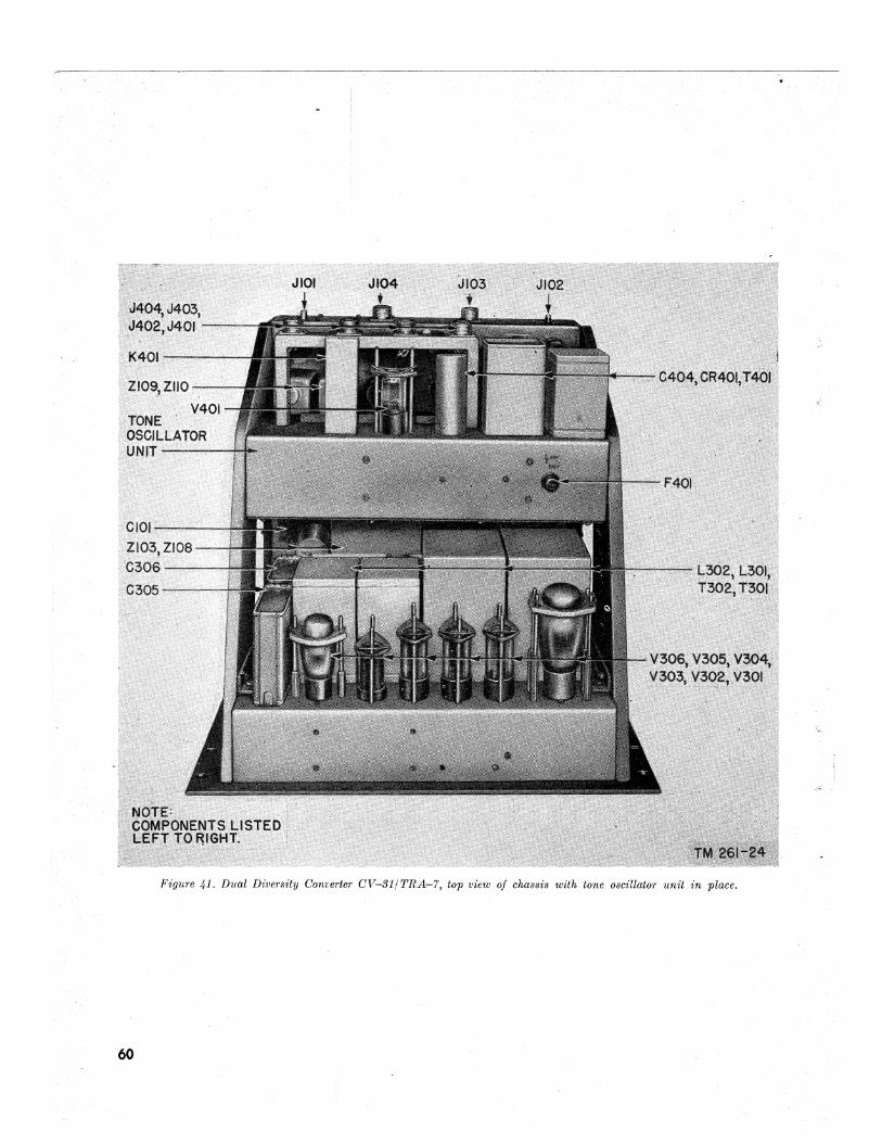
Figure 4-1. Dual Diversity Converter CV-31/TRA-7, top view of chassis with tone. oscillator unit in place.
60
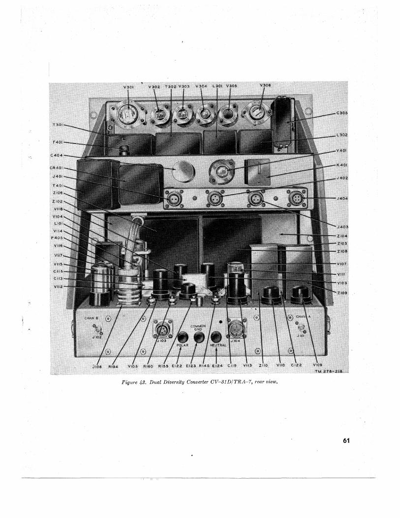
Figure 42. Dual Diversity Converter CV-31D/TRA-7, rear view.
61
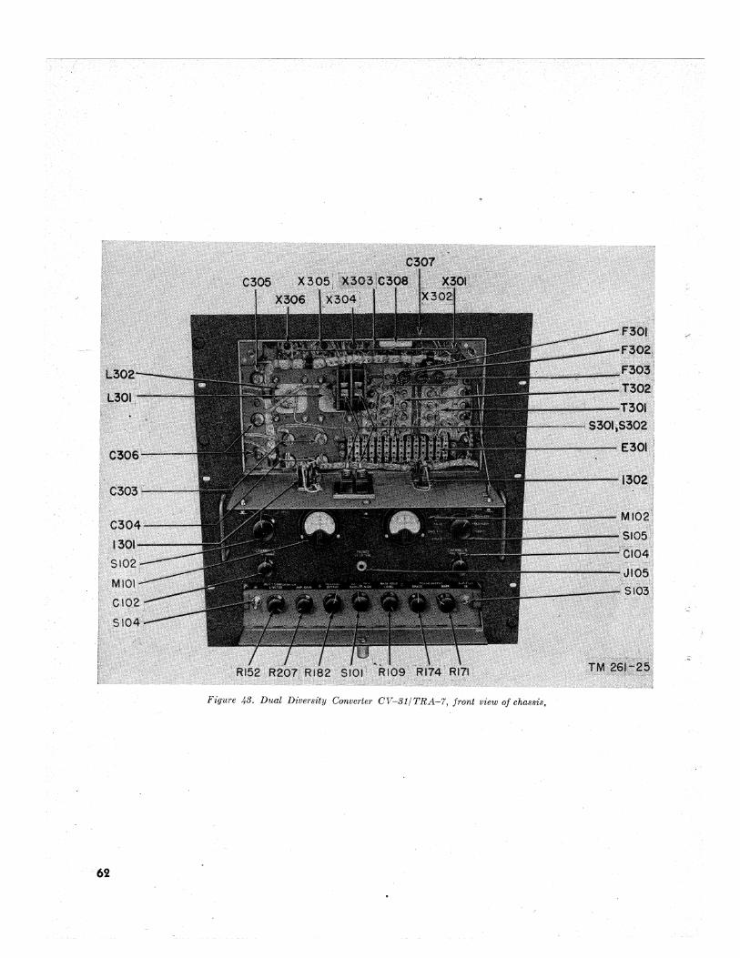
Figure 43. Dual Diver8ity Converter CV-31/TRA-7, front view of chassis,
62
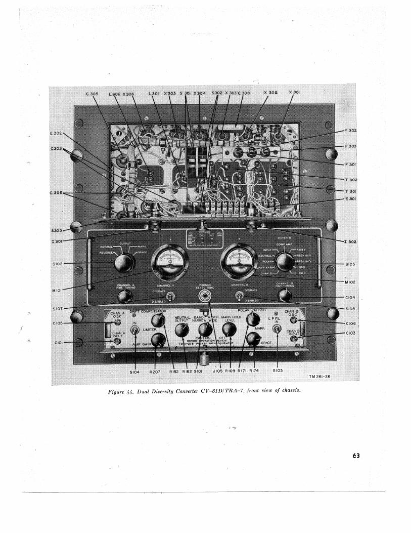
." .. ,.
!
Figure 44. Dual Diversity Converter CV-S1D/TRA-7, front view of chassis.
-1.1 II
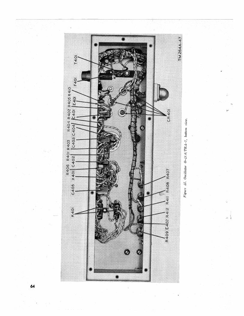
'" r
~ ., . .,. '" ~
~ ..c
1:--"
~ ~ ...... ...; ,....
"" ~ ... c ] ~
" ., 0
..c;;
"" ., ... ;:! .~
""
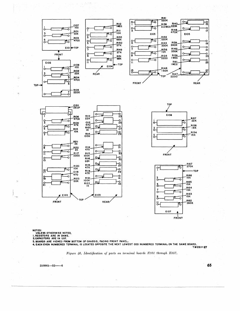
FRONT
TOP
FRONT
NOTES: UNLESS OTHERWISE NOTED,
I. RESISTORS ARE IN OHMS. 2.CAPACITORS ARE IN UUf.
CI07 100
RIOI 22K
RI03 4700
'TOP
CI08 100
RI02 22K
RI04 4700
RI05 2200
REAR
RI21 lOOK R�22-li-!'-'_-----'
IK
REAR
TOP
c3. BOARDS ARE VIEWED FROM BOTTOM OF CHASSIS, FACING FRONT PANEL.
REAR
TOP
EI06
~-----~~~~~~
~========::::!...J.-RI58 18K
~========::::!...J.-RI54 15K
FRONT
RI63 ,.-----,...._-r I~K r----~~~~~~K
EI07
FRONT
TOP
4. EACH EVEN NUMBERED TERMINAL IS LOCATED OPPOSITE THE NEXT LOWEST 000 NUMBERED TERMINAL ON THIt SAME BOARD. TM261-27
Figure 46. Identification of parts on terminal boards El01 through E107.
210961-52--6 65
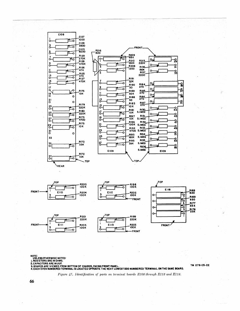
EI08
~"oo ~"'-i~;;;
~.w' "'''-1 :;1;;;;
NOTE: UNLESSOTHERWISE NOTED:
I. RESI STORS ARE IN OHMS. 2.CAPACITORS ARE IN UUF.
TOP RI9a lOOK
EII8 R202 lOOK
FRONT
RI99 220K
R203 FRONT lOOK
FRONT
3. BOARDS ARE VIEWED FROM BOTTOM OF CHASSIS ,FACING FRONT PANEL. 4. EACH EVEN NUMBERED TERMINAL IS LOCATED OPPOSITE THE 'N~XT LOW EST COD NUMBERED TERMINAL ON THE SAME BOARD.
Figure 47. Identification of parts on terminal boards ElOs through EllS and E11s.
66
RI68 820
RI&9 820 RITT UK RIT8 33K
-<
TM 278-C!I-22
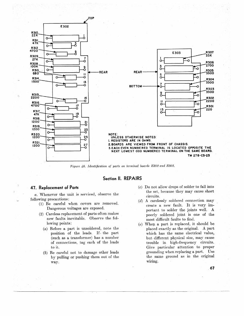
: '
!
R310 22K
R311 47K
R312 4700
R309 27K
R319 1200
E302
REAR REAR -----.I
BOTTOM --~~n....J
NOTE:
R307 33K
R306 2700
R305 3300
R304 3300
R303 3300
R302 2200
R301 220
R320 1200 UNLESS OTHERWISE NOTED:
R321 1200
I. RESISTORS ARE IN OHMS, 2.BOARDS ARE VIEWED fROM fRONT Of CHASSIS. 3.EACH EVEN NUMBERED TERMINAL IS LOCATED OPPOSITE THE
NEXT LOWEST ODD NUMBERED TERMINAL ON THE SAME BOARD.
TM 278-C5-25
Figure 48. Identification of p,arts on terminal boards E302 and E303.
Section II. REPAIRS
47. Replacement of Parts a. Whenever the unit is serviced, observe the
following precautions: (1) Be careful when covers are removed.
Dangerous voltages are exposed. (2) Careless replacement of parts often makes
- new faults Inevitable. Observe the following points:
(a) Before a part is unsoldered, note the posi~ion of the leads. If, the part (such as a transformer) has a number of connections, tag each of the leads to it.
(b) Be careful not to damage other leads by pulling or pushing them out of the way.
I, I
(c) Do not allow drops of solder to fall into the set, because they may cause short circuits.
(d) A carelessly soldered connection may create a new fault. It is very important to solder the joints well. A poorly soldered joint is one of the most difficult faults to find.
(e) Whe:tl a part is replaced, it should be placed exactly as the original. A part which has the same electrical value, but diff,erent physical size, may cause trouble in high-frequency circuits. Give particular attention to proper grounding when replacing a part. Use the same ground as in the original wiring.
67
b. The following repair instructions p'ertain specifically to Dual Diversity Oonverter OV-31 (*)/TRA-7:
(1) To replace eithel' of the two band-pass filters (Z105 or Z107) which are close to the front panel of the unit, it is necessary to remove the adjacent band-pass filter (either Z106 or Z108). To replace any of the apparatus in the power unit (other than the vacuum tubes), it is necessary to remove the tone oscillator unit (figs. 42 and 43) completely. This can be accomplished readily by loosening the two supporting bolts with hexagonal heads located on either side of the panel. In addition, it is necessary to discO'nnect the cable assemblies attached to the rear of the tone oscillator unit.
(2) When replacing the. OHANNEL A and OHANNEL B FINE TUNING knobs, aline shaft slot with dot on front panel. then fasten knob on shaft with pointer to the right.
48. Special Tools
Two types of special tools are provided as part of Dual Diversity Oonverter OV-31(*)/TRA-7.
a. One special potentiometer adjusting tool is provided to adjust the various screw-driver potentiometer controls shown in figure 5. It is located along the right-hand side of the panel of the chassis. These controls also may be adjusted by means of a screw driver.
b. Two hexagonal wrenches are provided to ad-. just the setscrews which retain the various control knobs to their shafts. One of these wrenches is located under the lower hinge cover which covers the controls on the front of the panel. The other is located at the extreme rear of the chassis. A third wrench is supplied with the lettered models; .it is located on the under side of the chassis, adjacent to the switch actuating cam with which it is associated.
c. Special tools for maintaining relay K401 are listed in paragraph 50a(4).
68
49. Wiring Diagrams
The wIring diagrams for the dual diversity converter are shown in figures 63 through 70.
a. In figures 63, 64, and 67, each piece of apparatus has the same designation as that stamped on the equipment, and the wiring terminals on each piece of apparatus are shown in their proper relative locations as viewed from the wiring side. The diagrams use ~he airline system of showing connections. With this system, each piece of apparatus is numbered arbitrarily, and feed lines representing the individual wires are carried a short distance and terminated at a common line running at right angles to the feed lines. These feed lines are marked with the color of the wire and have a number near the base line. This number is the same as the number of the piece of apparatus to which the other end of the wire 'Connects. It is not necessary to trace a connection through the common or base line, and nO' provision is made for doing so. By observing the color and the identification number, it is possible to move directly to the O'ther end of the wire.
b. In figures 65, 66, 68, and 70, a modified airline system is used to show connections. Each jumper wire that is not included as a part of a component subassembly is designated by a symbol and is represented by a line running from terminal to terminal. The description and the method of dressing each wire is indicated in a table on the diagram. In the diagram, a cable harness assembly is represented by parallel lines with cross hatching. Points where a wire or wires emerge from the cable harness assembly are designated stations and are numbered in sequence along the cable. At the point where a wire emerges from a station, its color code is indicated, and there is a number which indicates the distant station from which the other end of the wire ultimately emerges. By observing the color code and station reference designations at one end of the wire, it is possible to locate the other end quickly. This is also true for all wires which are a part of a cable harness assembly.
Section III. MAINTENANCE AND REPAIR OF RELAY K401
50. General InFormation and Cleaning Note. Keep the cover on the relay except when it is
necessary to remove it for trouble shooting or repair.
a. Ceneral.
(1) Relay K401 is a quick operating U-type relay. The adjustment requirements for U-type relays are both mechanical and electrical. The mechanical requirements include the proper position of springs, armature travel, spring tensions, etc. The electrical requirements are the specified currents through the winding which should cause the relay to operate or to release from the operated position. Different requirements are usually specified fOr test and for readjustment. Use the test values if it is necessary to check the relay when trouble shooting, otherwise use the readjustment requirements.
(2) Relay K401 is equipped with twin sets of contacts on each pair of mating springs. One spring each pair is split (bifurcated) near the contact end to permit means for setting the contacts so that both pairs
.. make and break at approximately the same point of spring travel. Use of twin contacts provides much greater protection against failure caused by lint or dirt between the contacts, provided the springs are adjusted properly so that parallel contacts make at the same time. The armatures of these relays are not fastened rigidly at the rear as in other types of relays, but are held in place by hinge pins' (bearings) (figs. 49 and 51). In this method of construction, the armature is not fixed rigidly as to position unless the relay is energized. Therefore, when checking the requirements requiring that the armature be in the operated position, the armature must be operatcd electrically rather than mechanically to insure accuracy of gaging.
(3) The relay winding and spring terminals are numbered on the schematic diagrams. The numbering plan for a typical U -type relay is shown in figure 51. The contact spring and winding terminals are numbered consecutively from right to left, facing the terminal side of the relay.
The top and bottom spring assemhlies of the relay each are numbered in sequence. The schematic diagrams show the top and bottom relay spring pile-ups, respectively, above and below the relay core and winding. A relay-winding terminal is followed by the letter T or B to indicate whether it is alined with the top or bottom spring-terminal pile-ups.
(4) The tools and gages used for adjusting relay K401, or burnishing its contacts, are given in the chart below. All codes are Western Electric.
Tools and gages Description
474A ________ Hexagonal closed-end offset . wrench Oi6" x X") ..
505A__ _ _ _ _ _ _ Spring adjuster for thin (,013")
507A (2 required).
265C _______ _ 70D ________ _ 132-type ____ _ KS-6528 ____ _ KS-6320 ____ _
b. Cleaning.
springs. Spring adjuster for springs other
than .013". Contact burnisher. 50--0-50 gram gage. Thickness gage. Cleaning tape. Orange stick.
(1) Failure of a circuit may be traced to particles of dirt or lint between contacts, or to dirty parts of a relay. A cover is provided to reduce, as far as possible, the entry of foreign materials and their accumulation on the working parts of the relay. When the cover is replaced on the relay, it should be replaced right side up, as determined by the designations on the cover, so as to avoid depositing dirt and lint from the bottom of the cover on the relay contacts and parts. When relays are cleaned, the inside of the cover should be wiped clean with a lint-free cloth.
(2) Carbon tetrachloride may be used, if available, to remove grease or oil from contacts. Deposit small drops of the carbon tetrachloride on the contacts with a toothpick. Do not rub. Be careful not to spill any of the liquid on the spoolheads and insulators. After contacts have thoroughly dried, burnish them to remove all foreign matter.
69
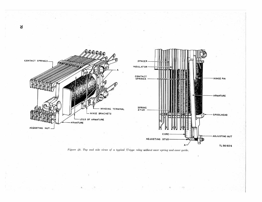
~
SPACER ::::::::::~,
INSULATOR ::: :: :: :::::: .. I
CONTACT SPRINGS .:: !:.:: ::.:: i 1----HINGE PIN
f---- ARMATURE
SPRING STUD :::::::: I:,
~SPOOLHEAO
AO,l';STlNG NUT
CORE .. II ADJUSTING STUD ~~ADJUSTING NUT
TL56160S
Figure 49. Top and side views of a typical U-type relay without cover spring and cover guide.
ti, (I ;~:J \.::)
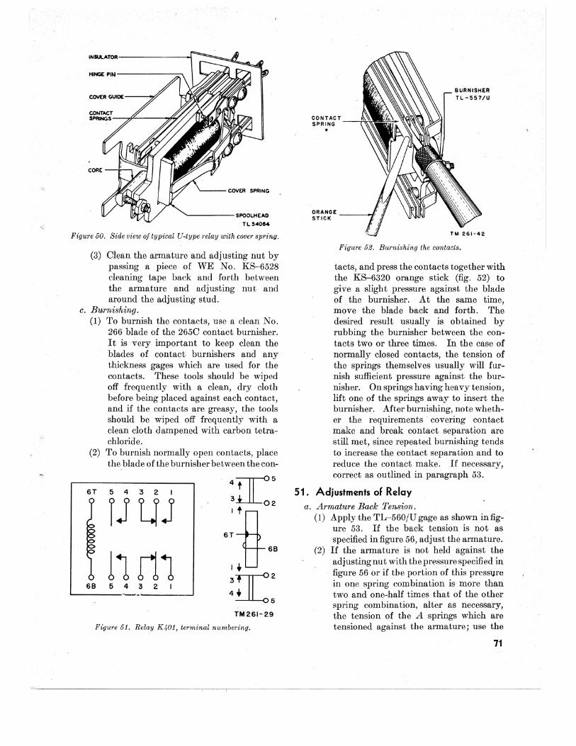
':"":
~roR------------~
HNGE PIN ------------:: ....
COVER GUIDE-. -...,...,,~
"---- COVER SPRING
......... --------SPOOLHEAD
TLS<IOI4
Figure 50. Side view of typical U-type relay with cover sprino.
(3) Olean the armature and adjusting nut by passing a piece of WE No. KS-6528 cleaning tape back and forth between the armature and adjusting nut and around the adjusting stud.
c. Burnishing. (1) To burnish the contacts, use a clean No.
266 blade of the 2650 contact burnisher. It is very important to keep clean the blades of contact burnishers and any thickness gages which are used for the contacts. These tools should be wiped off frequently with a clean, dry cloth before being placed against each contact, and if the contacts 'are greasy, the tools should be wiped off frequently with a clean cloth dampened with carbon tetrachloride.
(2) To burnish normally open contacts, place the blade of the burnisher between the con-
4IJC5 6T 5 4 3 2
jJ UJ 3 02
'i 6T
11 r11 68
,i-
3;:[' 68 5 4 3 2 4i-
5
TM261-29
Figure 51. Relay K401, terminal numbering.
~~~~NA;T_--+"",,, •
Figure 52. Burnishing the contacts.
tacts, and press the contacts together with the K8-6320 orange stick (fig. 52) to give a slight pressure against the blade of the burnisher. At the same time, move the blade back and forth. The desired result usually is obtained by rubbing the burnisher between the contacts two or three times. In the case of normally closed contacts, the tension of the springs themselves usually will furnish sufficient pressure against the burnisher. On springs having heavy tension, lift one of the springs away to insert the burnisher. After burnishing, note whether the requirements covering contact make and break contact separation are still met, since repeated burnishing tends to increase the contact separation and to reduce the contact make. If necessary, correct as outlined in paragraph 53.
51. Adjustments of Relay a. Armature Back Tension.
(1) Apply the TL--560jU gage as shown infigure 53. If the back tension is not as specified in figure 56, adjust the armature.
(2) If the armature is not held against the adjusting nu t with th e press~re specifi ed in
. figure 56 or if the portion of this pressure in o:q.e spring com bina tion is' more than two and one-half times that of the other spring combination, alter as necessary, the tension of the A springs which are tensioned against the armature; use the
71
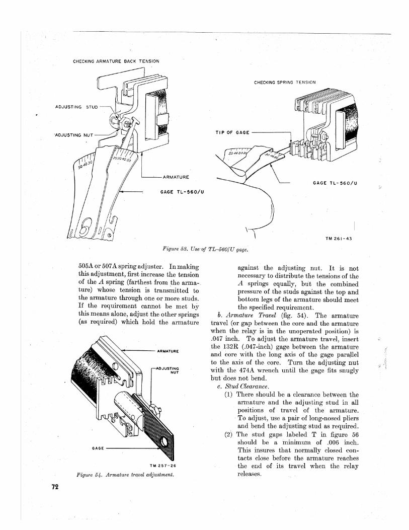
CHECKING ARMATURE BACK TENSION
CHECKING SPRING TENSION
ADJUSTING STUD
·ADJUSTlN.G NUT TI P OF GAGE -------,
l...-~_ ARMATURE GAGE TL- 560/U
GAGE TL-560/U
TM261-43
Figure 53. U8e 'oj TL-560jU gage.
72
505A or 507 A spring adjuster. In making this adjustment, first increase the tension of the A spring (farthest from ~he arma-. ture) whose tension is transmitted to the armature through one or more studs. If the requirement cannot be met by this means alone, adjustthe other springs (as required) which hold the armature
Figure 54. Armature travel adju8tment.
against the adjusting nut. It is not necessary to distribute the tensions of the A springs equally, but the combined pressure of the studs against the top and bottom legs of the armature should meet the specified requirement.
b. Armature Travel (fig. 54). The armature travel (or gap between the core and the armature when the relay is in the unoperated position) is .047 inch. To adjust the armature travel, insert the 132R (.047.-inch) gage between the armature and core with the long axis of the gage parallel to the axis of the core. Turn the adjusting nut with the 474A wrench until the gage fits snugly but does not bend.
c. Stud Clearance. (1) There should be a clearance between the
armature and the adjusting stud in all positions of travel of the armature .
. To adjust, use a pair of long-nosed pliers and bend the adjusting stud as required.
(2) The stud gaps labeled T in figure 56 should be a minimum of .006 inch. This insures that normally closed contacts close before the armature reaches the end of its travel when the relay releases.
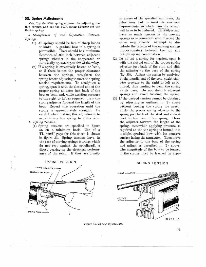
52. Spring Adjustments Note. Use the 505A spring adjuster for adjusting the
thin springs, and use the 507 A spring adjuster for the thicker springs.
a. Straightness of and Separation Between Springs.
(1) All springs should be free of sharp bends or kinks. A gradual bow in a spring is permissible. There should be a minimum clearance of .008 inch between adjacent springs whether in the unoperated or electrically operated position of the relay.
(2) If a spring is excessively bowed or bent, or ·if there is not the proper clearance between the springs, straighten the spring before adjusting to meet the spring tension requirements. To straighten a spring, span it with the slotted end of the proper spring adjuster just back of the bow or bend and, while exerting pressure to the right or left as required, draw the spring adjuster forward the length of the bow. Repeat this operation until the spring is approximately straight. Be careful when making this adjustment to avoid tilting the spring to either side.
b. Spring Tension. (1) Spring tensions are specified in figure
56 on a minimum basis. Use of a TL-560jU gage for this check is shown in figure 53. Spring tensions have, in the case of moving springs (springs which do not rest against the spoolhead), a direct bearing on the electrical performance of the relay. If they are greatly
SPRING POSITION
SPRING ADJUSTERS
SPRING TANG
in excess of the specified minimum, the relay may fail to meet its electrical requirement;;, •. iuw-hich case the tension will have to be reduced. Iii're'ltdjusting, have as much tension in the moving springs as is consistent with meeting the other requirements. Attempt to distribute the tension of the moving springs proportionately between the top and bottom spring combination.
(2) To adjust a spring for tension, span it with the slotted end of the proper spring adjuster just back of the stud and slide the adjuster to the base of the spring (fig. 55). Adjust the spring by applying, at the handle end of the tool, slight sidewise pressure to the right or left as required, thus tending to bend the spring at its base. Do not disturb adjacent springs and avoid twisting the spring.
(3) If the desired tension cannot be obtained by adjusting as outlined in (2) above without bowing the spring too much, apply the proper spring adjuster to the spring just back of the stud and slide it back to the base of the spring. Draw the adjuster forward the length of the spring, meanwhile applying pressure as required so the the spring is formed into a slight gradual bow with its concave surface facing the armature. Then move the adjuster to the base of the spring and adjust as described in (2) above. The magnitude of the bow to be formed in the spring must be learned by expe-
SPRING TENSION
SPRING ADJUsrER -----J:...,.,.fJ~~~
CONTACT SPRINGS __ -.-J
TM 257- 10
Figure 55. Spring adjustments.
73
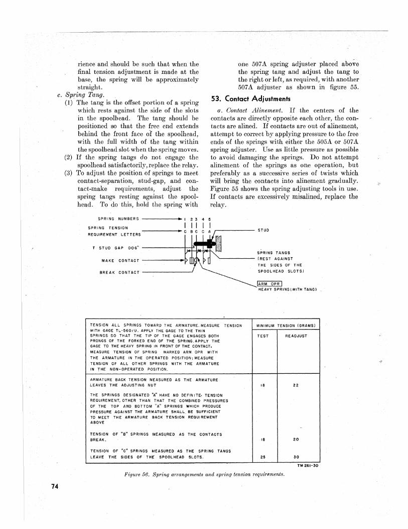
rience and should be such that when the final tension adjustment is made at the base, the spring will be approximately straight.
one 507 A spring adjuster placed above the spring tang and adjust the tang to the right or left, as required, with another 507 A adjuster as shown in figure 55.
c. Spring Tang. 53. Contact Adjustments
74
(1) The tang is the offset portion of a spring which rests against the side of the slots in the spoolbead. The tang should be positioned so that the free end extends behind the front face of the spoolhead, with the full width of the tang within the spoolhead slot when the spring moves.
(2) If the spring tangs do not engage the spoolhea,d satisfactorily, replace the relay.
(3) To adjust the position of springs to meet contact-separation, stud-gap, and contact-make requirements, adjust the spring tangs resting against the spoolhead. To do this, hold the spring with
(J. Contact Alinement. If the centers of the contacts are directly opposite each other, the contacts are alined. If contacts are out of alinement, attempt to correct by applying pressure to the free ends of the springs with either the 505A or 507 A spring adjuster. Use as little pressure as possible to avoid damaging the springs. Do not attempt alinement of the springs as one operation, but preferably as a successive series of twists which will bring the contacts into alinement gradually. Figure 55 shows the spring adjusting tools in use. H contacts are excessively misalined, replace the relay.
SPRING NUMBERS -------< •• I 23 4 5
SPRING TENSION I I I I I
RE:U~R:uM:N:A:EToToE:,S-------<"~ .. Ul ~,-! _____ :::,~" '''"'
MAKE CONTACT - ~ ~ ~t - (REST AGAINST 7 THE SIDES OF THE
BREAK CONTACT --------' SPOOLHEAD SLOTS)
TENSION ALL SPRINGS TOWARD THE ARMATURE. MEASURE TENSION WITH GAGE TL"560fU. APPLY THE GAGE TO THE THIN SPRINGS SO THAT THE TIP OF THE GAGE ENGAGES BOTH PRONGS OF THE FORKED END OF THE SPRING. APPLY THE GAGE TO THE HEAVY SPRING IN FRONT OF THE CONTACT.
MEASURE TENSION OF SPRING MARKED ARM.OPR WITH
THE ARMATURE IN THE OPERATED POSITION\ MEASURE
TENSION OF ALL OTHER SPRINGS WiTH THE ARMATURE
IN THE NON-OPERATED POSITION.
ARMATURE BACK TENSION MEASURED AS THE ARMATURE
LEAVES THE ADJUSTING NUT
THE SPRINGS DESIGNATED "A" HAVE NO DEFINITE· TENSION
REQUIREMENT, OTHER THAN THAT THE COMBINED PRESSURES
OF THE TOP AND BOTTOM "A" SPRINGS WHICH PRODUCE
PRESSURE AGAINST THE ARMATURE SHALL. BE SUFFICIENT
TO MEET THE ARMATURE BACK TENSION REQUIREMENT ABOVE
TENSION OF "B" SPRINGS MEASURED AS THE CONTACTS
BREAK.
TENSION OF "c" SPRINGS MEASURED AS THE SPRING TANGS
LEAVE THE SIDES OF THE' SPOOL HEAD SLOTS.
IARM. OPR I HEAVY SPRING (WITH TANGl
MINIMUM TENSION (GRAMS)
TEST READJUST
18 22
18 20
25 30
TM 261"30
Figure 56. Spring arrangements and spring tension requirements.
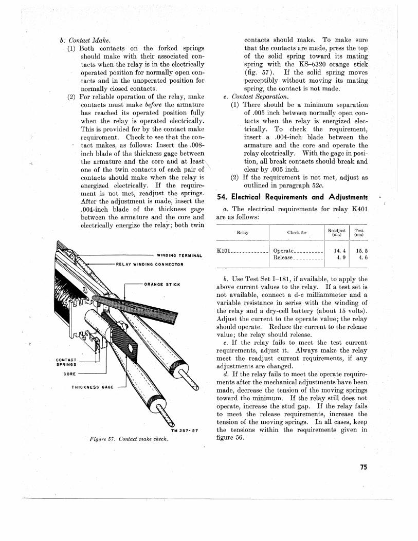
."
b. Oontact Make. . (1) Both contacts on the forked springs
should make with their associated contacts when the relay is in the electrically operated position for normally open contacts and in the unoperated position for normally closed contacts.
(2) For reliable operation of the relay, make contacts must make before the armature has reached its operated position fully when the relay is operated electrically. This is provided for by the contact make requirement. Check to see tpat the contact makes, as follows: Insert the .008-inch blade of the' thickness gage between the armature and the core and at leas~ one of the twin contacts of each pair of contacts should make when the relay is energized electrically. If the require:ment is not met, readjust the springs. After the adjustment is made, insert the .004-inch blade of the thickness gage between the armature and the core and electrically energize the relay; both twin
~I<!o:----------- WINDING TERMINAL
.~---RELAY WINDING CONNECTOR
CONT ACT --I-J SPRINGS
CORE---...J
TH ICKNESS GAGE
ORANGE STICK
Figure 57. Contact make check.
contacts should make. To make sure that the contacts are made, press the top of the solid spring toward its mating spring with the KS-b320 orange stick (fig. 57). If the solid spring moves. perceptibly without moving its mating spring, the contact is not made.
c. Oontact Separation. (1) There should be a minimum separation
of .005 inch between normally open contacts when the relay is energized elec-
. trically. To check the requirement, insert a .004-inch blade between the armature and the core and operate the relay electrically. With the gage in position, all break contacts should break and clear by .005 inch.
(2) If the requirement is not met, adjust as outlined in paragraph 52c.
54. Electrical Requirements and Adjustments
a. The electrical requirements for relay K40l are as follows:
Relay Oheck for Readjust I Test (rna) (rna)
]{lOI_____________ Operate _________ _ 14. 4 15. 5 Release _________ _ 4.9 4.6
b. Use Test Set 1-181, if available, to apply the above current values to the relay. If a test set is not available, connect a d-c milliammeter and a variable resistance in series with the winding of the relay and a dry-cell battery (about 15 volts). Adjust the current to the operate value; the relay should operate. Reduce the current to the release value; the relay should release.
c. If the relay fails to. meet the test current requirements, adjust it. Always make the relay meet the readjust current requirements, if any adjustments are changed.
d. If the relay fails to meet the operate requirements after the mechanical adjustments have been made, decrease the tensir)ll of the moving springs toward the minimum. If the relay still does not operate, increase the stud gap. If the relll>Y fails to meet the release requirements, increase the tension of the moving springs. In all cases, keep the tellElions within the requirements given in figure 56.
75
Section IV. ALiNEMENT 55. Basic Through B Converter Models
a. General. (1) The basic through B models of the dual
diversity converter are normally used with Radio Receiver Assembly OA-65(*)/MRO-2 or with two Radio Receivers R-336/GRC-26. Radio Receiver Assembly OA-65(*)/MRO-2 consists of a- common oscillator (Oscillator-Amplifier 0-59/MRO) and two receivers. These may be. Radio Receivers' R-182(*)/ MRO-2 or modified Radio Receivers BC-342-N.
(2) Frequency Meter BC-221-(*) or any standard r-f signal generator may be used to inject a test signal into either J101 or J102, the input jacks for channel A and channel B, respectively. For greatest accuracy use a spare Frequency Shift ExciLer 0-39(*)/TRA-7 in conjunction with a spare radio receiver as a source of r-f signals. The initial input should be approximately .1 volt if the converter is badly misalined. Because Frequency Meter BC-221-(*) provides only about 8 mv, it is not suitable for initial alinement. Instead, use any signal generator capable of providing .1 volt. Frequency Meter BC-221-(*) may be used for determining the exact frequency of the receiver i. f. and for setting a signal generator to that frequency. Final alinement should be performed, using the receivers that will be associated with the convcrter during actual use. The following instructions assume that the receivers have already been alined and the receiver intermediate frequencies are peaked at 470 kc.
b. Alinement oj Channel A Input Circuit. Tune in a strong r-f carrier with receiver A. Reduce the volume of receiver B to zero. Set the receiver on MVO, the CRYSTAL PHASING control fully clockwise to OUT, and the C. W.-OSC. switch to OFF. The bandwidth control (if provided in the receiver) should be at 8 kc.
76
(1) Tune the VERNIER of receiver A for the exact center of the 470-kc i-f pass band. To find the center of the pass band, use one of the following methods:
(a) Inject a modulated r-f signal into the receiver antenna terminals, noting the
output on the output power meter; the output meter should be connected across the loudspeakcr input terminals. The signal generator frequency is rocked for maximum indicatIon on the output power meter. After this IS
accomplished, the modulation IS
switched off for subsequent tests. (b) Determine the VERNIER readings for
the outsides of the pass band and set the VERNIER control midway between these limits.
(c) The following accurate method involves the use of the ORYSTAL PHASING control on the receiver and can be used only if a strong r-f carrier is prescnt.
1. Find _ the approximate center of the i-f pass band of the receiver with the VERNIER control. The c-w oscillator may be used to locate the signal but should be turned off for all
. subsequent adjustments. 2. Turn the CRYSTAL PHASING con
trol counterclockwise until the audio output is at a minimum. Keep the volume control at maximum.
S. Rock the VERNIER control until characteristic chirps or beats are heard in the output, indicating that the i-f input frequency is in resonance with the 470-kc crystal in the crystal phasing circuit. The loudspeaker may be used; however, at times the use of a headset with lower resultant volume may be desirable.
4. After the center of the i-f pass band is found, turn the CRYSTAL PHASING control clockwise to the OUT position and leave it there for all later operations.
(2) Turn METER B switch to INPUT and be sure CHANNEL A FINE TUNING control is straight up.
(3) Adjust capacitor 0105 (fig. 5) to obtain a maximum indication on meter B and a zero indication on meter A, indicating the center of the 50-kc discriminator characteristic. This center point can be verified on meter A by rotating the CHANNEL A FIKE TUNING control 90° to both sides of the straight up
J
position. The pointer should deflect approximately the same amount either side of zero and in the same direction that the knob is turned. The red markers on both ci~cillator capacitors C105 and C106 and input capacitors C101 and C103, when adjacent to the black dot on the chassis, indicate 'that the capacitor is at minimum capacitance. The plates of these capacitors should be almost completely unmeshed when the i. f. of the receiver is 470 kc. The oscillator of channel B may give a spurious response which will show up as input on meter B when the above adjustments are made. To guard against this trouble, remove tube V102 from its socket while making oscillator adjustments on channel A. The condition just described is a normal one, and should not cause concern on the part of the operator. This condition does not exist when final adjustments have been accomplished correctly. The input meter reading for input signals to the converter up to approximately .1 volt depends on the setting of BAND WIDTH switch. WIDE band position will give about half-scale reading with .02 to .025-volt input while NARROW band position requires approximately twice this value for a:o. eguivalent meter reading.
(4) After the proper oscillator frequency has been found, adjust the input circuit of the converter u~it by means of capacitor C101 for a maxinulm in.dication on meter B., If meter B goes off scale, decrease the
, volume of receiver A. (5) Repeat the alinement of capacitor C105
as in (3) above. If proper adjustments have been made, it should be possible to swing the CHANNEL A FINE TUNING control to either side of straight up and down and obtain deflections on meter A. The input level shown on meter B should be maximum when meter A is at zero. . The level should decrease slightly as meter A travels away from zero in either direction. The same results should' 'be obtained when the receiver VERNIER control is rotated to both sides of the position of exact frequency. Check to see that meter A
deflects to the left when the CHANNEL. A FINE TUNING control is turned to the left, and deflects to the right when" the FINE TUNING control is turned to the right.
c. Alinement of Ohannel B Input Oircuit. The method of adjustment for channel B is identicai to that used for channel A, except that the input level and the discriminator output cannot be read simultaneously. Both are read on meter B, depending on the position of the METER B switch:
(1) Turn the volume control of receiver B to maximum and the volume control of receiver A to minimum.
(2) Locate the center of the i-f pass band as described in a(l) above.
(3) Reinstall tube V102 if it was removed. (4) Set METER B switch at INPUT and
locate the approximate oscillator frequency by adjusting capacitor '0106 to obtain a maximum reading on meter B. The oscillator of channel A may give a spurious response which will show up as input on meter B when adjusting. To guard against this trouble, remove tube V101 from channel A while making oscillator adjustments on channel B. The con.dition is a normal one, and should not cause concern on the part of the operator. This condition does not exist when the final adjustments have been correctly accomplished.
(5) Adjust capacitor C103 for maximum reading on meter B.
(6) Turn METER B switch to CHAN B. (7) Set CHANNEL B FINE TUNING
control in a straight up position. (8) Readjust oscillator capacitor C106 to
obtain a zero reading on meter B, thus indicating the center of the 29.3-kc discriminator char'acteristic. Vary the FINE TUNING control 900 to either side and note that meter B swings approximately equal distances either side of zero. The meter swing should be in the same direction in which the CHANNEL B FINE TUNING control is turned.
(9) Return METER B switch to INPUT and again vary the CHANNEL B FINE TUNING control 90° to poth sides of straight up. Note that the input level is maximum when the control is straight
77
up, ~nd decreases ouIya small amount when the control is moved 90 0 to either side of straight up position.
(10) Reinstall tube V101 if it was removed. d. Alinement oj Output Circuit. The alining
adjustments should be made with a strong i-f signal input to the dual diversity converter (0.02 volt or more). The alinement steps indicated in (1) through (4) below can be performed with no signal input if tube V105 is removed from Dual .Diversity Converter CV-31/TRA-7 or if the MARK-HOLD LEVEL control is turned completely counterclockwise in Dual Diversity Converters CV-31A/TRA-7 andCV-31B/TRA-7, to disable the mark-hold circuit· while adjustments are made.
78
(1) Turn the OUTPUT switch to MARK and the METER B switch to NEUTRAL.
(2) Adjust the NEUTRAL OUTPUT control knob for a reading of +60 on meter B.
(3) Turn the METER B switch to POLAR and adjust the POLAR OUTPUT MARK control knob for a reading of +25 on meter B.
(4) Turn t4e OUTPUT knob to SPACE and adjust the POLAR OUTPUT SPACE knob for a reading of -:25 on meter B.
(5) Turn the OUTPUT knob to NORMAL or REVERSE, and throw the DRIFT COMPENSATOR switch to IN.
(6) . Turn the limiter knob to maximum clock'wise position, and turn the AMP GAIN knob and the COMP AMP screw driver control fully counterclockwise.
(7) Feed a strong steady 470-kc signal into channel A of the converter, and adjust the signal strength so that with the CHANNEL A FINE TUNING control in the straight up position, meter A will read zero (center of discriminator output).
(8) Return the METER B switch to POLAR and adjust the BIAS A screw driver control (R155) to a point where the polar output current indicated on meter B just changes from mark to space and then vice versa. Set the control to midposition between the· two points found. This adjusts the d-c output loop to have an operating point corresponding to about 0 volt from the discriminator.
(9) Turn the METER B switch to CHAN
A+B. Meter B should read 0 within ±10.
(10) Turn the COMP AMP control (R145) slightly clockwise until meter B indicates about 5 divisions higher than the reading obtained in (9)· above.
(11) Turn the BIAS B screw driver control (R160) back and forth until the meter B reading just changes from 5 below the reading established in (9) above to 5 above the reading established in (10) above. For instance, if the reading obtained in (9) above was +6 and the adjustment of the COMP AMP control gave + 11, the limits are + 1 and + 11.
(12) Set the BIAS B control halfway between the points which provide the limit readings. With the BIAS A and BIAS B screw driver controls set, and the METER B knob at CHAN A + B, turn the COMP AMP screw driver control until meter B indicates +70 or -70.
(13) Turn the AMP GAIN knob clockwise until the output can be changed from a mark to a space or vice versa by a fast movement of the CHANNEL A (or CHANNEL B) FINE TUNING knob. Restore the CHANNEL A (or CHANNEL B) FINE TUNING knob to a straight up position (zero reading on meter A).
(14) Turn the COMP AMP screw driver control (R145) for a +70 or -70 reading on meter B; then turn the COMP BAL screw driver control (R194) for a balance. Repeat until alternate equal indicatioml are obtained at +70 and -70 when CHANNEL A FINE TUNING is given a fast movement.
(15) Slowly turn the LIMITER knob counterclockwise until the indication on meter B starts to drop below 70. Set the LIMITER knob at the point where the meter reading just barely starts to reduce.
56. Converter Models c; and. 0 The·following instructions assume that the
radio receivers already have been alined so that the i-f output stages of the receivers are peaked at 500 kc. The following alinement procedures will be based on a steady r-f carrier being fed into receiver A (or receiver B, if desired) and that the
receiver has been calibrated so that the i-f input to the converter is exactly 500 kc. For bench tests, a suitable signal generator or Frequency Meter BC-22I-(*) can be used to inject a strong i-f carrier into the input connections of the dual. diversity converter. However, final alinement should be performed, using the associated receivers. Connect channel A and channel B receivers to jacks JIOI and JI02. The AC SUPPLY and PLATE switches are set to their ON.positions.
a. Alinement and Adjustment Equipment. The equipments necessary for the alinement and adjustment of the dual diversity converter are Radio Receivers R-388-fURR, normally used with these converter models, and a screw driver.
b. Channel A Input Circuit. (1) Set CHANNEL A disabling switch to
OPERATE and CHANNEL B disabling switch to DISABLED.,
(2) Turn the METER B switch to the INPUT position with the CHANNEL A FINE TUNING control pointer in the straight up position.
(3) Open the hinged door on the front panel (fig. 4) and adjust capacitor CI05 (CHAN A OS C) with a screw driver for a maximum indication on meter B and a zero indication on meter A. This indicates the center of the 50-kc discriminator characteristics and may be verified on meter A by rotating the CHANNEL A FINE TUNING control 90° to the left and to the right of the straight up position. The meter indicator will deflect approximately equal amounts to the left and to the right of zero in unison and in phase with the control pointer.
(4) After the oscillator frequency adjustment has been made, adjust the CHANNEL A input circuit. With a screw driver, adjust capacitor C1OI, CHAN A INPUT, for a maximum indication on meterB. If meter B goes off scale, decrease the RF GAIN Of receiver A.
(5) Repeat the alinement of capacitor C105 as in (3) above.
(6) When proper adjustments have been made, it will be possible to turn the CHANNEL A FINE TUNING control to either side of the straight up position and obtain deflections on meter A. The input-level indication on meter B should be maximum when meter A indicates
zero. The level should decrease slightly as meter A travels away from zero in in either direction. The same results should be obtained when the 'receiver tuning control is rotated to either side of the position of exact frequency.
(7) Oheck to see that meter A deflects to the left when the CHANNEL A FINE TUNING control is turned to 'the left and deflects to the right when the FINE TUNING control is turned to the right. If the meter deflections are reversed, it will be necessary to repeat (3) through (7) using a different setting' of CI05. The correct setting of C105 is the place where a second maximum peak is shown onmeterB.
c. Channel B Input Circuit. The method of adjusting channel B is identical to' that used for channel A except that the input level and the discriminator output cannot be read simultaneously. Both are read on meter B, depending on the position of the METER B switch.
(1) Turn the RF GAIN control of receiver B to maximum and CHANNEL A disabling switch to DISABLED and the CHANNEL B disabling switch to OPERATE.
(2) Set METER B switch to INPUT and locate the approximate oscillator frequency by adjusting capacitor 0106, CHAN B OSO (fig. 4), to obtain a maximum reading on meter B.
(3) With a screw driver, adjust' capacitor CI03 (OHAN B INPUT) to obtain a maximum reading on meter B.
(4) Turn METER B switch to CHAN B. Set the OHANNEL B FINE TUNING control to a straight up position. Readjust oscillator capacitor C106 (CHAN B OSO) to obtain a zero reading on meter B, thus indicating the center of the 29.3-kc discriminator characteristic. Vary the FINE TUNING control 90° to either side of zero. Check to see that the indicator of meter B deflects to the right of zero when the OHANNEL B FINE TUNING control is turned to the right and deflects to the left of zero when the CHANNEL B FINE TUNING control is turned to the left.
(5) Return METER B switch to INPUT and again vary the OHANNEL B FINE
79
TUNING control 90° to either side and note that the input level is maximum when the control is straight up and decreases only a small amount as the control is moved 90° to either side of the straight up position.
(6) Restore operation of channel A by placing the OHANNEL A disabling switch in the OPERATE position.
d. Output Circuits. The following adjustments should be made with a strong i-f signal input to the dual diversity converter. The alinementcovered in the steps indicated in (1) through (3) below, however, can be performed with no signal input if the MARK HOLD LEVEL switch is set to the OFF position.
80
(1) Set the OUTPUT switch at MARK and the METER B switch at NEUTRAL. Adjust the NEUTRAL OUTPUT control knob for a reading of +60 on meter B.
(2) Turn the 'METER B switch to POLAR and adjust the POLAR OUTPUT MARK control knob for a reading to +25 on meter B.
(3) Turn the OUTPUT knob to SPAOE and adjust the POLAR OUTPUT SPAOE knob for a reading of -25 on meter B.
(4) Turn the OUTPUT knob to NORMAL or REVERSE, and turn the DRIFT COMPENSATOR switch to IN. Turn the LIMITER knob to the maximum clockwise position, and turn the AMP GAIN knob and the OOMP AMP screw driver control fully counterclockwise.
(5) Feed a strong, steady 500-kc signal into channel A of the converter and adjust the signal strength so that with the OHANNEL A FINE TUNING control pointer in the straight up position, meter A will indicate zero (center of discrIminator output).
(6) Return the METER B switch to POLAR and adjust BIAS A screwdriver control R155 (fig. 5) to a point where the polar output current indicated on meter B just changes from mark to space, and then vice versa. Set the control to ruidposition between the two points found.
Note. This adjusts the d-c output loop to have an operating point' corresponding to about a O-volt output from the discriminator.,
(7) Turn the METER B switch to OHAN A + B. Meter B should read 0 within ±1O:
(8) Turn the OOMP AMP control (fig. 5) slightly clockwise until meter B indicates about five divisions higher than the 'rea~-ing obtained in (7) above. .
(9) Turn BIAS B screw driver control R160 (fig. 5) back and forth until the meter B reading just changes from 5 below the reading established in (7) above to 5 above the reading established in (8) above. For instance, if the reading obtained in (7) above was + 6 and _ the adjustment of the OOMP AMP control (8 above) gave +11, the limits are +1 and +11.
(10) Set the BIAS B control halfway between the points which provide the limit readings. 'With the BIAS A and BIAS B screw driver controls set and the METER B knob at OHAN A + B, turn the COMP AMP screw driver control until meter B indicates +70 or -70.
(11) Turn the AMP GAIN knob clockwia~ until the output can be changed from a mark to space, or vice versa, by a fast movement of the OHANNEL A (or CHANNEL B) FINE TUNING knob. Restore the CHANNEL A (or CHANNEL B) FINE TUNING knob to straight up position (zero reading on meter A).
(12) Turn the COMP AMP screw driver control (RI45) to +70 or -70 on meter B, then turn the COMP BAL screw driver control (RI94) for balance. Repeat until alternate equal indications are obtained of +70 and -:--70 when OHANNEL A FINE TUNING knob is given a fast movement.
(13) Slowly turn the LIMITER knob co~nterclockwise until the indication on meter B starts to drop below 70. Set the LIMITER knob at the point where the meter reading is just barely starting to reduce.
(14) The final adjustment of the AMP GAIN control requires an input of miscellaneous keying.
(a) Turn the METER B switch to OOMP AMP position.
(b) Turn the AMP GAIN knob fully counterclockwise and then, when miscellaneous signals are being received, slowly turn the knob clockwise while observing METER B for a minimum of irregular deflections or kicks. The normal setting will usually be 30° or 40° from the counterclockwise stop for 850-cycle frequency shift. Set the AMP GAIN knob in a position which provides a keyed tone output from the converter and results in minimum kicks on ~1ETER B. A more accurate setting of thc AMP GAIN knob may be found if the LIMITER knob is first turned fully clockwise.
(c) Turn the METER B switch to the OHAN A + B position.
(d) Verify that the deflection on meter B, on a steady mark signal, is 70 to the right of zero, and during a steady mark signal, reset the LIMITER knob to a position which causes the 70 indication to just start to decrease.
(e) Oonnect a headphone to the PHONES KEYED TONE jack, and verify that clear distinct tones are produced. Olear distinct tones indicate the absence of noise peaks or distortion caused by improper tuning.
57. Adjustment of Power Supply
The power supply and the converter are connected together by means of E30I; 1I5-volt a-c (alternating-current) power input jack JI04 is located at the rear of the converter. Thc' input power is connected to the power transformers and all power for the operation of the converter is obtained from the power supply. Oonnect the 115-volt a-c source to jack JI04 of the converter by means of a cord such as Oord OX-954/TRA-7. Make sure that the a-c power is connected to the proper terminals of transformers T30I and T302. Set the AO SUPPLY power switch to ON and the PLATE switch to ON. A 20,000-ohm-pervoltmeter is used for measuring the voltages of the power supply.
a. Regulated -150-Volt Supply. (1) In the converter, connect a 2,000-ohm
resistor between binding posts EI22 and EI23 (or pins A and B of JI03). Oon-
nect an I,800-ohm resistor between binding posts EI24 and E123 (or pins D and E of J103); strap out resistors R184 through R187.
(2) Set the OUTPUT switch to MARK and METER B switch to POLAR, and adjust the POLAR OUTPUT MARK conti'ol so that meter B registers +25. Set the OUTPUT switch to SP AOE and METER B switch to NEUTRAL, and adjust the NEUTRAL OUTPUT control so that meter n registers +60.
(3) Oonnect the voltmeter between terminal 11 of terminal strip E301 and ground of the power supply.
(4) The voltmeter should indicate between -145 and -160 volts when the two conditions indicated in (1) and (2) above are satisfied.
b. Regulated +150-Volt Supply. (1) Repeat a(I).and a(2) above. (2) In the converter, set the OHANNEL A
and OHANNEL B disabling switches to operate (0 and D models).
(3) Oonnect the voltmeter between terminal 4 of terminal strip E30I·and ground.
(4) If the voltage is more than 3 volts greater than (disregarding the polarity) the voltages indicated in a(4) above, strap out portions of resistance provided by resistors R312 through R315 until the terminal 4 voltage matches the terminal 11 voltage within 3 volts.
(5) If the voltage is more than 3 volts less than (disregarding the polarity) the voltage indicated in a(4) above, strap out resistor R3I6 first and then strap out resistors R3I2 through R315 as required to match the voltages.
c. Bias Voltage jor Output Tubes. (1) Oonnect the voltmeter between pin 5 of
V116 and the junction point of two of the series of resistors (R162 through RI67). Oheck for equal readings when S102 is switched from SP AOE to MARK.
(2) Repeat the above procedure at different junction point8~lIltil the equal readings are obtained.
(3) Move the lead coming from the grids of V116 and V117 to junction point determined by the above tests.
81
Section V. FINAL TESTING
58. General
This section is'intended as a guide to be used in determining the quality of a Dual Diversity Converter CV-31(*)jTRA-7 repaired at higher echelon levels. The minimum test requirements outlined in the following paragraphs may be performed by maintenance personnel with adequate test equipment and the necessary skills. Repaired equipment meeting the specifications in the paragraphs below will furnish uniformly satisfactory results during operation. The tests given in paragraphs 62 through 73 should be performed in the order given.
59. T e~t Equipment Required
a. The following items of test equipment are required to perform the tests in this section:
Multimeter T8-352jU or equal. Electronic Multimeter ME-6AjU or equal. Audio Oscillator TS-382A/G or equal. Signal Generator TS-588jU or equal. Headset of 2,000 to 4,000 ohms impedance. Oscilloscope OS-8AjU or equal. Distortion Test Set TS-383jGG or equal. Variac (variable primary power source for the
converter) capable of supplying 175 watts. . Teletypewriter TT-55jMGC or equal.
b. If a large number of converter units are to be tested, consideration should be given to obtaining the following additional equipments:
82
Converter test cabinet, WE #SID-I07077 or equal.
Transmitter-distributor, Teletype #14-F or . equal.
Transmission measuring set, WE #SID-· 107040 or equal.
Set of patch cords, consisting of-One WE #SID-117103AM, three con
ductor, with Hubbell plug and twist lock ends.
Four WE #SID-117102E, two conductor, with WE #347 ends.
One WE #SID-117113B, five conductor, with AN-14S-5P ends.
One WE #SID-II7113M, four conductor, with AN-14S-10P and AN-14S-10S ends.
One WE #SID-117113N, four conductor, with AN-14S-11P and AN-14S-11S ends.
60. Preliminary Operations
a. Check to see that all switch de tents operate properly.
b. The pointers on the CI02 and CI04 knobs should point to the left when the capacitors are meshed fully.
c. Check to see that T301 and T302 are connected for 115-volt operation.
d. Make up the leads shown in figure 58. Resistors should be of at least 5-watt size.
61. Converter Stage Voltage Tests
a. Connect the input power cord of the variac to a 115-volt source. Connect JI04 to the variac. Throw the AC SUPPLY switch to the ON position. The white pilot lamp should light. Adjust· the converter line voltage to 115 volts by means of the variac.
b. Place a shorting clip between terminal 4 of V117 and terminal 12 of terminal strip E301 (-400-volt input lead). Leave terminal 4 of Vl17 connected to terminal 5 of V116 but remove the connection between these grid leads and the R162 to R167 resistor string.
c. Throw the PLATE switch to ON. The red pilot lamp should light.
d. Connect the test set-up shown for JI03 in figure 58. Open switches SI and S2. Strap out resistors R184 through R187. Connect the external milliammeter to the POLAR LOOP jack. Adjust the POLAR OUTPUT MARK control (on the converter unit) for a current of +25 rna while the OUTPUT switch is at MARK. Transfer the milliammeter to the NEUTRAL LOOP jack and adjust the NEUTRAL OUTPUT control for a 60-ma reading.
e. Set the OUTPUT switch at MARK and measure the voltage from terminal 11 of E301 to the chassis (ground). The voltage should be between-145 and -160 volts. Make a note of this voltage.
f. Measure the voltage from terminal 4 of E301 to the chassis. This voltage should be within ± 3 volts of that measured in e above, but of positive polarity. Make a note of this voltage.
(1) If the voltage difference is too high, strap out enough of resistors R312 through R315 to bring the voltage within the 3-volt limit
(2) If the voltage is too low, first strap out
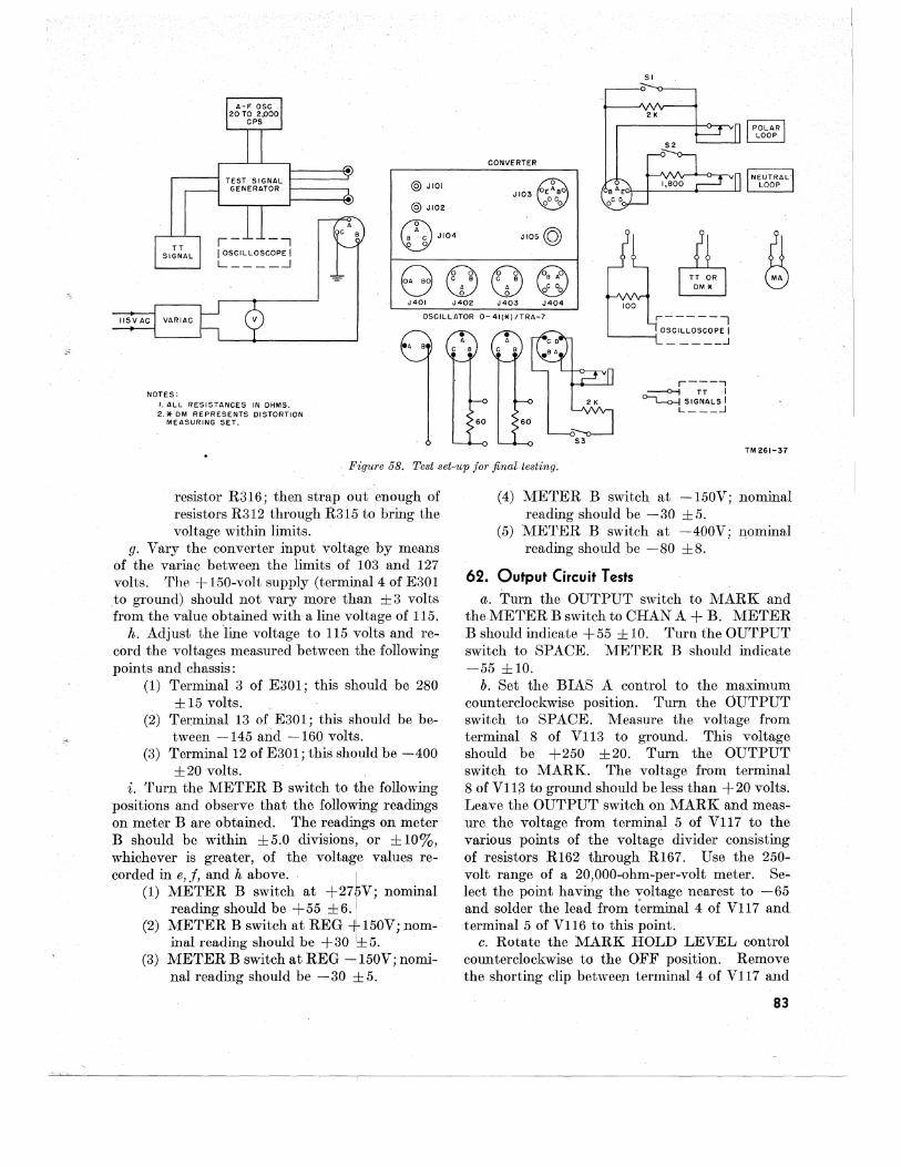
r- --, I OSCILLOSCOPE I
@ JIOI
@ JI02
~J104
SI
2K
~IOS©
L ____ --1
OG)Q@ ,t!, .. ~: @ G J401 J402 J403 J404 100
OSCILLATOR 0- 41("'/TRA-7 ,-----, L-----i OSCILLOSCOPE I
NOTES: I. ALL RESISTANCES IN OHMS. 2.* OM REPRESENTS DISTORTION
MEASURING SET.
e. 8
_____ ...J
r----, ~ TT I ~SIGNALSI
L ___ ...l
TM 261-37
. Figure 58. Test set-up for final testing.
resistor R316; then strap Qut' enough of resistors R312 through R315 to bring the voltage within limits. .
g. Vary the converter input voltage by means of the variac between the limits of 103 and 127 volts. The + 150-volt supply (terminal 4 of E301 .to ground) should not vary more than ±3 volts from the value obtained with a line voltage of 115.
h. Adjust the line voltage to 115 volts and record the voltages measured between the following points and chassis:
(1) Terminal 3 of E301; this should be 280 ±15 volts.
(2) Terminal 13 of E301; this should be between -145 and -160 volts.
(3) Terminal 12 of E301; this should be -400 ±20 volts.
i. Turn the METER B switch to. the following positions and observe that the following readings on meter B are obtained. The readings on meter B should be within ± 5.0 divisions, or ± 10%, whichever is greater, of the voltage values re-corded in e, j, and h above. . I
(1) METER B switch at +27pV; nominal reading should be +55 ±6.!
(2) METER B switch at REG +150V; nom-inal reading should be +30 ~ 5. .
(3) METER B switch at REG -150V; nominal reading should be ....,..30 ±5.
(4) METER B switch at -150V; nominal reading should be -30 ±5.
(5) METER B switch at ~400V; nominal reading should be -80 ±8.
62. Output Circuit Tests a. Turn the OUTPUT switch to MARK and
theMETERB switch to CHAN A + B. METER B should indicate +55 ± 10. Turn the OUTPUT switch to SPACE. METER B should indicate -55 ±10.
b. Set the BIAS A control to the maximum counterclockwise position. Turn the OUTPUT switch to SPACE. Measure the voltage from terminal 8 of V113 to ground. This voltage should be +250 ±20. Turn the OUTPUT switch to MARK. The voltage from terminal 8 of V113 to ground should be less than +20 volts. Leave the OUTPUT switch on MARK and measure the voltage from termin~l 5 of V117 to the various points of the voltage divider consisting of resistors R162 through R167. Use the 250-volt range of a 20,000-ohm-per-volt meter. Select the point having the voltage nearest to -65 and solder the lead from terminal 4 of V117 and. terminal 5 of V116 to this point.
c. Rotate the MARK HOLD LEVEL control counterclockwise to the OFF position. Remove the shorting clip between terminal 4 of V117 and
83
terminal 12 of E30l (this was inserted during the operation in paragraph 61b). Readjust the POLAR OUTPUT MARK control for a reading of +25 ma at the POLAR LOOP jack. Readjust the POLAR OUTPUT SP AOE control for a reading of -25 mao Measure the voltage to ground from terminal 8 of V117. With the OUTPUT switch at MARK, this should be between +210 and + 165 volts. With the OUTPUT switch at SP AOE, it should be between -135 and -160 volts.
d. Readjust the NEUTRAL LOOP current to 60 ma with the NEUTRAL OUTPUT control (OUTPUT switch at MARK). Operate the METER B switch to POLAR; it should indicate 25 ±3. With the OUTPUT switch at SPAOE, it should indicate to the·left and for mark signals it should indicate to the right.
e. Operate the METER B switch to NEUTRAL. The neutral output current should be indicated on meter B by a reading of 60 ±5 for a mark and 0 for a space. The mark reading should be to the right.
f. With switch Sl of the J103 circuit open, it should be possible to adjust for a polar output current of ±30 ma or greater. With the OUTPUT switch on MARK, switch 8-2 of the J103 circuit open, and resistors R184 through R187 strapped out, it should be possible to adjust for a neutral output·current of 63 ma or greater. Remove the strap from across R184 through R187 (applied during the operations in paragraph 61d).
g. Olose switches Sl and S2 of the J103 circuit. It should be possible to adjust the polar output currents to ±20 ma or less. With the OUTPUT switch on MARK, it should be possible to adjust the neutral output current to . +40 ma or less. Readjust the polar and neutral loop currents for ±25 ma and +60 ma, respectively.
63. Channel A Converter Tests a. Apply no input to J102 while testing channel
A. Set the r-f signal generator to 395 kc (440 kc for the C and D models) with a 1,000-mv output. Oonnect it to channel A input jack J101. Oonnect the VTVM from terminal 3 of Z103 to ground. Adjust capacitor 0101 for a marimum indication on the VTVM; this should be between 13 and 22 volts.
b. Oonnect the VTVM from terminal 2 of Z104 to ground. The voltage should be between 1.5 and 3.5 volts over the complete range of capacitor 0105.
84
c. Connect the VTVM from terminal 4 of E103 to ground. Set the BAND WIDTH switch to NARROW. Adjust capacitor 0105 to give a 0 reading on meter A. This should occur with the converter A oscillator section operating at 445 kc (490 kc in the 0 and D models) and capacitor 0105 set at nearly maximum capacitance. Set the r-f oscillator to lOO-mv output. The voltage read on the VTVM should be between 10 and 25 volts. Move the BAND WIDTH switch to WIDE. The VTVM should read between 20 and 40 volts.
d. Set the r-f signal generator to 475 kc (520 kc for the 0 and D models). Set the BAND WIDTH switch to NARROW. Adjust tuning capacitors 0105 and 0101 to give a maximum votage reading~ This should occur at a converter A oscillator frequency of 525 kc (565 kc for the 0 and D models). With an r-f input of 100 mv, the VTMV should read between 10 and 25 volts.
64. Channel B Converter Tests
Apply no input to JlOl while testing channel B. a. Apply the 1,000-mv, 395-kc (440 kc for the 0
and D models) signal to J102. Oonnect the VTVM from terminal 3 of Z101 to ground. Adjust capacitor 0 103 for marimumon the VTVM; this should be between 13 and 22 volts.
b. Oonn/ilct the VTVM between terminal 2 of Zl02 and ground. The voltage should be between 1.5 and 3.5 volts over the complete range of capacitor 0106.
C. Oonnect the VTVM from terminal 4 of E103 to ground. Set the BAND WIDTH switch to NARROW. Turn the METER B switch to OHAN B. Adjust capacitor 0106 to give a 0 reading on m,eter B. This should occur with the converter B oscillator section operating at 424.3 kc. (469.3 kc. in the 0 and D models) and capacitor 0106 set at nearly maximum capacitance. Set the r-f oscillator at 100 mv. The voltage reading on the VTVM should be between 10 and 25 volts. Move the BAND WIDTH switch to WIDE; the VTVM should read beteeen 20 and 40 volts.
d. Set the r-f signal generator to 475 kc (520 kc for the 0 and D .models). The converter B oscillator section will give a 29.3-kc i.f. at two points: 504.3 kc (549.3 kc in the 0 and D models) and 445.7 kc (490.7 kc for the 0 and D models). The higher oscillator frequency is used; this will be near the minimum capacitance settings of 0106 and 0103. Adjust these two capacitors for maximum voltage reading on the VTVM; with the BAND WIDTH switch at NARROW, this should be
between 10 and 25 volts; with the switch at WIDE, the reading should be between 20 and 40 volts.
65. -limiter Tests
a. Adjust the r-f signal generator to 450 kc (495 kc for the C and D models).
b. Set the BAND WIDTH switch at NARROW. Aline the channel A input and oscillator tuning as in paragraph 63, using the frequency specified in a above. Aline the channel B input and oscillator tuning as in paragraph 63, using the frequency specified in a above.
c. Set the METER B switch at INPUT. Adjust the output level of the r-f signal generator to give a meter B' indication of +50. There should be no input to channel B. The voltage measured at terminal 4 of E103 should not be greater than 6 volts. The signal required for the meter B reading of +50 should not be greater than 20 mv.
d. Without changing the input level to channel A connect the VTVM from terminal 42 of E103 to ground. The reading should be 6 ±2 volts.
e. Adjust the signal input to channel A to 0.5 mv. The VTVM should read more than 3.5 volts. Adjust the signal input to -500 mv; the VTVM should read 6 ± 2 volts.
j. Connect the oscilloscope from terminal 42 of E103 to ground. Make certain that the high input side of the oscilloscope is connected to ter~ minal 42. Shunt the vertical input with a 100-ohm resistor. Use a saw-tooth sweep frequency suitable to obtain a 3-cycle pattern. Observe that the waveform of the 50-kc signal output from the limiter is close to that shown in A, figure 35.
g. Repeat _ the tests in c through f above on channel B. Observe that the waveform of the 29.3-kc signal output from the limiter is close to that shown in B, figure 35. Remove the oscilloscope connections from terminal 42 of E103.
66. Discriminator Tests
a. Apply an input of 50 mv_at 450 kc to channel A. Set trimmer capacitor C102 at half capacitance. Adjust capacitor C105 to give a zero indication on meter A (center of discriminator range).
b. Apply an input of 50 mv at 450 kc to channel B (no input to channel A). Set trimmer capacitor C104 to half capacitance and adjust tuning capacitor C106 to give a zero indication on meter B. Make certain that the higher channel B, local, oscillator frequency is the one used to avoid inversion of the discriminator output in this channel.
Have METER B switch at the CHAN B position~ c. Operate the test signal circuit to spacing with
a frequency shift of 850 cps. By readjustment of the test oscillator frequency, center the mark and ' space readings of meter B around zero. Meter B will give equal indication of 50 ± 10 either side of zero and will indicate to the left for space. Shift the input from CHAN B to CHAN A, without readjustment of the r-f signal generator tuning controls,' and check to see that the above limits are met on meter A.
67. Drift Compensator Circuit
a. Adjust the signal generator for an input of 50 mv to CHAN A and no input to CHAN B.
b. With the DRIFT COMPENSATOR switch at IN, the OUTPUT switch at NORMAL, and the AMP GAIN control at its maximum counterclockwise position, turn the COMP AMP control to its extreme counterclockwise position. Turn the I.JIMITER control to its maximum clockwise position. Set the METER B switch at CHAN A + B. Meter B will read 0 ±5. Note this reading. Adjust the BIAS A control to a point where a marking or spacing loop condition :m.ay be obtained by just a slight movement of the BIAS A control as observed on meter B in the POLAR loop circuit. Adjust the BIAS A control to a point about halfway between the positions where the polar output changes from mark to space and from space to mark.
c. Set the METER B switch at CHAN A + B. Turn the COMP AMP control in a clockwise direction until the meter B reading is increased by 5 to the right or left depending on whether the circuit is in a marking or spacing condition. This reading will be to the right or left depending on the condition of the output circuits at the tinie the adjustment is made.
d. Turn the BIAS B control slowly to the two positions where meter B deflects to the right and to the left of the readings noted in b above. Set the BIAS B control midway between these two positions.
e. Set the COMP AMP control at midposition. Advance the AMP GAIN control until sending a mark or space from the test signal generator results in keying of the output loops. The output -switch should be at NORMAL. With METER B switch at CHAN A + B, meter B shall indicate to the right for mark and left for space.
j. Adjust the COMP BAL and COMP AMP controls to provide steady meter B readillgs of
- 85
I
+70 ±5 for mark and -70 ±5 for space. (Allow several seconds for each reading to stabilize.)
g. With the LIMITER control at maximum clockwise position, measure the voltage to ground from terminals 4 and 5 of V1l2 (use a d-c voltmeter). These voltages will be plus and minus 24 ±3 volts, respectively. With the COMP AMP control adjusted to give meter B indications of plus and minus 70 ± 5 for mark and space respectively, slowly reduce the LIMITER control until the meter B reading drops to. + 50 for mark. With this setting the reading for space will be -50 :!= 10. Turn the LIMITER control f lly clockwIse and then slowly counterclockwise until the meter B reading just begins to decrease.
h. Operate the DRIFT COMPENSATOR switch toOUT, the OUTPUT switch to REVERSE and METER B switch to CHAl\' B. Set the test set sending circuit to give centered deflections of the meters in the discriminator outputs. Set the MARK HOLD LEVEL switch in the on position. Send a steady space into either CHAN A or CHAN B at such a level to give a reading of 50 on meter B with the METER B switch at INPUT. Adjust the ~1ARK HOLD LEVEL control until the output circuit just remains spacing. Set the input le:vels into A and B so that an input reading of 50 on meter B is obtained from either input alone. Apply this level to both channels A and B. Observe that the loop circuit is in a spacing condition but restores to a marking cond'ition when the inputs to both A and B are reduced to zero.
i. With the converter adjusted for diversity balance as in j above, connect a receiving TT to the neutral loop circuit. Send miscellaneous siO"-b
nals from test generator on channel A; channels A + B, and channel B alone. Observe that the TT prints correct copy as the neutral loop current is varied between 55 and 65 ma at a converter input line voltage of 115 volts. Repeat for line voltages of 103 and 127 volts.
j. Place the OUTPUT switch at MARK and with neutral loop currents of 55 and 65 ma, operate the receiving TT keyboard and see that correct copy is printed. Repeat for line voltages of 103 and 127 volts.
Note. If the requirements of i and j above cannot be met,'refer to paragraph 61b and select the point on the voltage divider to provide the next lower voltage on terminal 4 of V117. Connect the lead to this point and recheck as in i and j above.
68. Over-all Transmission Tests
. The following test requires the equipment listed m paragraph 59b or an equivalent" test set-up.
a. Check that the converter circuit is adjusted for normal operation. Set the MARK HOLD LEVEL control to the OFF position. Check the test signal generator for a frequency shift of 850 cps at 450 kc. Adjust the input level to 50 mv. Check that the converter oscillators are alined correctly for the mean fr~quency to be used. Check that each input, channels A and B, in turn produces equal plus and minus discriminator output re~dings on meters A and B when the signal mput IS changed from M to S. Set the BAND WIDTH switch at NARROW.
b. Connect the oscilloscope from terminal 3 of V1l1 to ground. Remove the 100-ohm load resistor from across the vertical plates of the oscilloscope. Operate the DRIFT COMPENSATOR switch to OUT and the LP FIL to out. Set the OUTPUT switch at REVERSE. Set the signal switch on the test cabinet at DOTS. Patch from the output jack on the SID-107040 De:ade O~cillator to the a-f (audio-frequency) OSCIllator Jack on the test cabinet. Check the signal generator bias by patching the vertical input of the oscilloscope to the SCOPE jack on the generator. With the decade oscillator set at 20 cycle~, observe the waveform on the scope using a SUItable sweep frequency on the horizontal plates. By adjusting the decade oscillator output to approximately 0 dbm (decibels referred to a milliwatt in 600 ?hms) , and adjusting the generator's bias control, and the sweep frequency (with no synchronization), it should be possible to obtain a pattern similar to A, figure 61. In making the check, use 20 cps for 20 reversals (dots), 65 cps for 65 reversals, and 130 cps for 130 reversals.
c. Send 20-cycle reversals from the test circuit first on channel A only, and then on channel B only. Observe their waveshapes on the oscilloscope. They shoUld be nearly square as indicated in A, figure 59. Raise the dot frequency to 65. The waveform will appear as in B, figure 59. Observe the change in waveform when the LP FIL switch is operated to IN. This change should appear as in C, figure 59. Raise the dot frequency to 130. With the LP FIL switch at out the waveform should appear as in D, figure 59. Check that
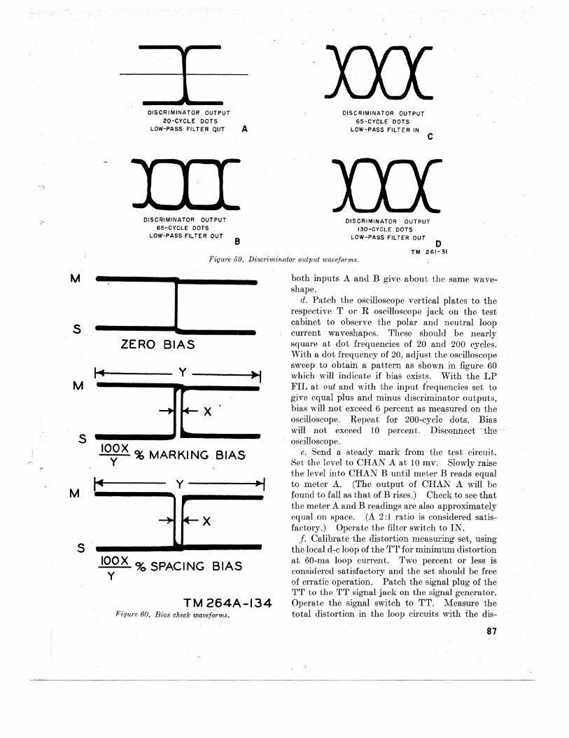
M
S
M
S
-"
'"'
M
S
DISCRIMINATOR OUTPUT
20-CYCLE DOTS LOW-PASS FILTER QUT A
DISCRIMINATOR OUTPUT 65-CYCLE DOTS
LOW-PASS FILTER OUT B
DISCRIMINATOR OUTPUT
6S-CYCLE DOTS LOW-PASS FILTER IN
c
DISCRIMINATOR OUTPUT 130-CYCLE DOTS
LOW-PASS FILTER OUT D
TM 261-31 Figure 59. Discriminator output waveforms.
ZERO BIAS
I ... y
--. I+-x .
IOOX % MARKING BIAS Y
l-t y
IOOX % SPACING BIAS Y
~I
~I
TM264A-134 Figure 80. Bias check '/faveforms.
both inputs A and B give about the same waveshape.
d. Patch the oscilloscope vertical plates to the respective T or R oscilloscope jack on the test cabinet to observe the polar and neutral loop current waveshapes. These should be nearly square at dot frequencies of 20 and 200 cycles. With a dot frequency of 20, adjust the oscilloscope sweep to obtain a pattern as shown in figure 60 which will indicate if bias exists. With the LP FIL at out and with the input frequencies set to give equal plus and minus discriminator outputs, bias will not exceed 6 percent as measured on the oscilloscope. Repeat for 200-cycle dots. Bias will not exceed 10 percent., Disconnect'tl:r~'-oscilloscope.
e. Send a steady mark from the test circuit. Set the level to CHAN A at 10 mv. Slowly raise the level into CHAN B until meter B reads equal to meter A. (The output of CHAN A will be found to fall as that of B rises.) Check to see that the meter A and B readings are also approximately equal on space. (A 2:1 ratio is considered satisfactory.) Operate the filter switch to IN.
j. Calibrate the distortion measuring set, using the local d-c loop of the TT for minimum distortion at, 60-ma loop current.' Two percent or less is considered satisfactory and the set should be free of erratic operation. Patch tl~e signal plug of the TT to the TT signal jack on the signal generator. Operate the signal switch to TT. Measure the total distortion in the loop circuits with the dis-
87
tortion measuring set by patching into the respective, REC jacks on the test cabinet. Use corresponding jacks on the test set, that is, use POLAR when testing the polar loop. . Send the test sentence and record the distortion in both polar and neutral loops for ch.annels A, A + B, and 'E. The distortion will not exceed 6 perC(lllt. In each case the maximum distortion observed over any half-minute period will be recorded as the distortion.
g. Operate the DRIFT COMPENSATOR switch to IN and the OUTPUT switch to NORMAL. Set the METER B switch at COMP AMP and note that minimum kicks are indicated in meter B when'the test sentence is being transmitted. Move the METERB switch from the COMP AMP position. Measure the distortion in the polar and neutral loops for channels A, A + B, and B while the test sentence is being transmitted. The distortion will not exceed 6 percent. Measure the distortion in the polar loop for· repeated BL and LTRS characters. These tests will indicate not. more than 6 percent distortion.
h. Operate the BAND WIDTH control to WIDE. Check that the DRIFT COMPENSATOR switch is at IN and the OUTPUT switch at NORMAL. Set the test oscillator to have frequencies 1,000 cps above and below the centered frequencies used in g above. The shift should remain at 850 cps. Make distortion measurements of the test sentence and repeated BL and LTRS characters for frequencies 1,000 cps above and below the original centered frequency settings. In each case the distortion will not exceed 6 percent. Return the BAND WIDTH switch to NARROW.
i. Repeat the tests of h above for channel A alone, channel B alone, and channel A + B with the BAND WIDTH switch at NARROW for frequencies +300 cycles and -300 cycles removed from the center operating frequency. The distortion will not exceed 5 percent.
69. Low Signal Input Tests
a. Make the adjustments specified in paragraph 68a, at a signal input level of .5 mv for channel A and channel B. Complete the tests described in paragraph 68b and c. Use a test signalgenerator frequency of 470 kc in the basic through A models and a 500-kc frequency for the C and D models for final alinement.
88
b. Without changing the input-level settings, connect the test generator circuit to both CHAN A and CHAN B, operate the LP FIL switch to IN, and make the tests of TT signal distortion (miscellaneous signals only) specified in paragraph 68j through h. The distortion will not exceed 6 percent. Measure the distortion for channel A and for chaIlIltlI B also.
70. Low Frequency Shift Tests
Make the test specified in paragraph 68j and g for channel A only and then for channel B only, using a 100-cycle frequency shift instead of an 850-cycle shift. Use miscellaneous signals only. The distortion will not exceed 5 percent. The output from the test signal generator should be 2.0 mv for channel A and channel B.
71. Tone Oscillator and Control Relay Tests
a. Adjust relay K401 to operate on a current of 15 to 17 rna and release on a current of 9.0 to 11.5 rna. Connect a 2,000-ohm resistance across the control loop leads from connector J401. If the equipment in paragraph 59b is used, the following patching arrangements should be made:
(1) Place a dummy plug in the CON jack. (2) From J404 on test cabinet toJ404 on
the tone oscillator. (3) From J403 on test cabinet to J403 on
the tone oscillator. (4) From J402 on test cabinet to J402 on
the tone oscillator. (5) From J401 on test cabinet to J401 on
the "tone oscillator. b. The CON lamp in the test set should be
lighted. Place the test cabinet meter switch at CON RELAY. Operate the CON KEY. Relay K401 should operate. The test set meter should read 90 ± 10 which is equivalent to 45 ± 5 volts. The CON LAMP should be extinguished.
c. Read the receiver disabling relay circuit voltages across the 60-ohm resistances connected across J402 and J403. This is done by closing the CON KEY and setting the test cabinet meter at CON-1 and then CON-2. In each case the meter should read between 9.0 and 10.25 when the a-c line voltage is 115 volts. Release the CON KEY.
d; Connect a 2,OOO-ohm headset to the PHONES KEYED TONE jack on the converter. Observe that a tone signal is obtained when the 60-ma loop of the converter is in a marking
{)ondition. . No tone will be heard for a space {)ondition. Measure the tone voltage obtained at the ~HONES KEYED TONE jack with the VTVM. The voltage will be 1 ±O.5 volts. Check both sides to ground. Measure the frequency of the tone output by comparison with an audio oscillator on an oscilloscope. The frequency will be 850 ± 100 cps.
e. Send a space from the test circuit at a level of 50mv to both channel A and channel B. Set the OUTPUT ·switch at REVERSE and the DRIFT COMPENSATOR switch at out. Operate relay K401 as in b above. The loops
210961-'112-7
will change to marking conditio.m.. Set the DRIFT COMPENSATOR at IN and the OUTPUT switch at NORMAL (in this order). Operating relay K401 shall again change the loops from space to mark. This last test cannot be repeated again without first restoring the circuit by operating the OUTPUT switch to Reverse and back to NORMAL.
j. Operate the OUTPUT switch to SPACE. Connect the source of TT signals to the CON jacks on the test panel. The distortion measured in the polar and neutral loops will not exceed 5 percent.
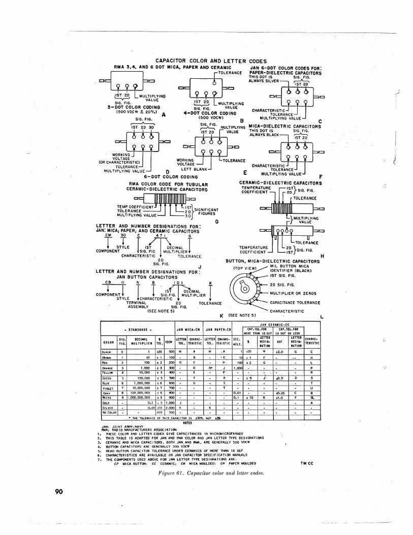
90
CAPACITOR COLOR AND LETTER CODES RMA 3,4, AND 6 DOT MICA, PAPER AND CERAMIC .JAN 6~DOT COLOR CODES FOR:
THIS DOT IS SIG. FIG. ALWAYS SILVER ,---f\--,.
1ST 20' ~OLfRANC~ PAPER-DIELECTRIC CAPACITORS
SIG. FIG. ,---JI---.,. 1ST 20 3D
C MICA-DIELECTR IC CAPACITORS
WORKING VOLTAGE
(OR CHARACTERISTIC) TOLERANCE
MULTIPLYING VALUE 0
THIS DOT IS SIG. FIG. ALWAYS BLACK Is12ii'
6-DOT COLOR CODING
RMA COLOR CODE FOR TUBULAR CERAMIC-'DIELECTRIC CAPACITORS
E F
CERAMIC-DIELECTRIC CAPACITORS TEMPERATURE 1ST} COEFFICIENT 20 SIG. FIG.
k S;LsIGNIFICANT 3 OJ FIGURES
G LETTER AND NUMBER DESIGNATIONS FOR' JAN: MICA; PAPER; AND CERAMIC CAPACITORS'
TCM T IC ([}471 rG,
STYLE 1ST DECIMAL COMPONENT SIG. FIG. ,MULTIPLIER
CHARACTERISTIC TOLERANCE
TEMPERATURE COEFFICIENT
TOLERANCE
20 SIG. FIG.
BUTTON, MICA-DIELECTRIC CAPACITORS
J 'LETTER AND NUMBER DESIGNATIONS FOR:
JAN BUTTON CAPACITORS
cl 111 IN IB , IS
COMPONENT SIG. FIG. STYLE CHARACTERISTIC t
TERMINAL 20 TOLERANCE ASSEMBLY SIG. FIG.
(SEE NOTE 5) K (SEE NOTE 5)
MIL BUTTON MICA IDENTIFIER (BLACK) 1ST SIG. FIG.
20 SIG. FIG.
MULTIPLIER OR ZEROS
CAPACITANCE TOLERANCE
CHARACTERISTIC
JAN CERAMIC.CC
• STANDARDS. JAN MICA.CM JAN PAPER.CM CAP. TOl.FOR CAP. TDL.FOR MORE THAN 10 UUF 10 UUF OR LESS
SIG. DECIMAL ~ LETTER CHARAC· LETTER CHARAC· DEC. LETTER LETTER CHARAC· COLOR FlO. MULTIPLIER TOl. YDCW TDl. TERtSTIC TOl. TERISTIC MOLT.
~ DES Ill· UUF OESI6- TERISTIC RATIOII MAIIOM
BlACK 0 I .20 500 M A M .A I .20 M .2.0 G C
eRCMN I 10 ., 100 B • E 10 • I F .- H
RED 2 100 • 2 200 G C - H 100 .2 G - L
OR .... 3 1.000 ,3 300 D NO J 1.000 - P
YELU" • 10.000 •• 400 'E P - - R
GREEN 5 100,000 .5 500 F - R ,5 .i , to. 5 D S
BWE 6 1.000.000 .6 600 G S ,- T
VIOLET 7 10.000.000 ,7 700 T - - - U
GoAy 8 100,000,000 ,8 BOO 0.01 - .0.25 {: B
"ITE 9 1.000.000.000, ,9 900 0.1 , 10 K t-I.O F 51
GeL. 0.1 , 5 1.000 J - - A
SILVER 0.01 ,,0 Z.OOO K K - - -NO CoLOR " '20 500 -
•. THE TOLERANCE OF lltiS CAPACITOR IS :1:301. NOT oS ROTES
JAN: JOINT ARMY. NAVY RMA, RAD 10 MANUFACTURERS ASSOC IATION
I. THESE COLOR AND LETTER COOES GIVE CAPACITANCES IN MICROMICROFARADS 2. THIS TABLE IS ADAPTED FOR JAN AND RMA COLOR AND JAN LETTER TYPE DESIGNATIONS 3. CERAMIC AND MICA CAPACITORS. BOTH JAN AND RMA. ARE GENERALLY 500 VDCW 4. BUTTON CAPACITORS ARE GENERALLY 300 vDcw 5. READ BUTTON CAPACITOR TOLERANCE UNDER CERAMICS OF MORE THAN 10 WF 6. CHARACTERISTICS ARE AVAILABLE -IN JAN CAPACITOR SPECIFICATION MANUALS 7. THE COMPONENTS USED ABOVE FOR JAN L£TTER TYPE DESIGNATIONS ARE,
Cl' MICA BUTTON, CC CERAMIC, CII MICA MOULDED, CN PAPER MOULD~D TM CC
Figure 61. Capacitor color and letter codes.
H
L
"(
)
I
J
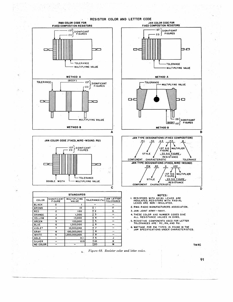
RESISTOR COl-OR AND LETTER CODE RMA COLOR CODE FOR
FIXED COMPOSITION RESIST()RS
1ST} :;IGNIFICA, NT 20 FIGURES
Cl
TOLERANCE
MULTIPLYING VALUE
MULTIPLYING VA,LUE
METHOD B
A
JAN COLOR CODE FOR FIXED COMPOSITION RESISTORS
I iT }SIGNIFICANT 20 FIGURES
TOLERANCE
L-----MULTIPLYING VALUE
JAN TYPE DESIGNATIONS (FIXED COMPOSITION)
B
JAN COLOR CODE (FIXED, WIRE-WOUND: RU)
,!Re T30~~s: rGLTlPL~'~,R,"""::"",,,
COLOR SIGNIFICANT FIGURE
BLACK 0 BROWN I
RED 2
ORANGE 3
YELLOW 4
GREEN 5
BLUE 6
VIOLET 7
GRAY B WIiITE 9
GOLD -SILVER -NO COLOR -
TOLERANCE - MULTIPLYING VALUE
STANDARDS
MULTIPLYING, TOLERANCE!"!.) VALUE
I -10 +1
100 +2
1,000 !3
10,000 !4 100,000 !5
1,000,000 !6
10,000,000 + 7
100,000,000 +B
1,000,000,000 :!:9
0.1 +5
'0.01 !IO "!20
C
,.
JAN LETTER TOLERANCE
-F
G
-
-
J K M
FIGU~~ ! MUI "
STYLE , 20 SIG/IGURE , RESISTANCE
COMPONE-NT CIiARACTERISTIC TOLERANCE
JAN TYPE DESIGNATIONS (FIXED, WIRE-WOUND)
"
RW r4°h~ST roLTIPLIER FIGUS~~!MUI
STYLE ,20 SIG/IGURE , c RESISTANCE
COMPONENT CIiARACTERISTIC
NOTES: I. RESISTORS WITII AXIAL LEADS ARE
INSULATED. RESISTORS WITII RADIAL LEADS ARE NON - INSULATED.
2. RMA: RADIO MANUFACTURERS ASSOCIATION.
3. JAN: JOINT ARMY - NAVY.
4. TIIESE COLOR AND NUMBER CODES GI.VE ALL RESISTANCE VALUES IN OIl'MS.
, 5. RESISTIVE COMPO~ENTS USED FOR LETTER TOLERANCES ARE: RC,RN,AND RU.
6. WATTAGE FOR RW TYPES IS FOUND IN TilE JAN SPECIFICATIONS UNDER CIIARACTERISTICS.
...... ,
D
TMRC
Figure 62. Resistor color Q,nd letter codes.
91
CHAPTER 5
SHIPMENT AND LIMITED STORAGE AND DEMOLITION TO PREVENT ENEMYlUSE
Section I. SHIPMENT AND LIMITED STORAGE
72. General The exact procedure in repacking for shipment
or limited storage depends upon the material available· and the conditions under which the equipment is to be shipped or stored.
73. Repacking for Shipment or limited Storage Whenever practicable, place a dehydrating
agent such as silica gel inside the chests or packing boxes. Protect the chests (or boxes) with a waterproof paper barrier. Seal the seams of the paper barrier with waterproof sealing c9mpound or tape. Pack the protected chests in a padded wooden case, providing at least 3 inches of excelsior padding or some similar material between the paper barrier and the packing case.
Section II. DEMOLITION OF MATERIEL TO PREVENT ENEMY USE
74. General The demolition procedures outlined in paragraph
75 ·will be used to prevent the enemy from using or salvaging the equipment. Demolition of the equipment will be accomplished only upon order of the commander.
75. Methods of Destruction a. Smash. Smash the controls, tubes, switches,
capacitors, transformers, and case, liSing sledges, axes, handaxes, pickaxes, hammers, crowbara, or heavy tools.
92
b. Out. Out chassis wiring, using axes, handaxes, or machetes. ..
c. Burn. Burn resistors, capacitors, wiring, and technical manuals, using gasoline, kerosene, e>il, flame throwers, or incendiary grenades.
d. Bend. Bend panels, cabinet, and chassis. e. Explosives. If explosives are necessary, use
firearms, grenades, or TNT. j. Disposal. Bury or scatter the destroyed
parts in slit trenches, fox holes, or other holes, or throw them into streams.
g. Other. Destroy everything.
APPENDIX I i
REFERENCES Ii
I . Note. For availability of items listed, check SR 310-20-3, SR 310-21-4, and SR 310-20-5.
Army Supply Catalog SrG 1 for Signal Corps Supply Catalogs. Check Department of the
1. Army Regulations
AR 380-5
AR 750-5
2. Supply Bulletins
SB 11-6
SB 11-47
SB 11-76
Military Security (Safeguarding Military Information) .
Maintenance of Supplies and Equipment (Maintenance Responsibilities and Shop Operation).
Dry Battery Supply Data.
Preparation and Submission of Requisitions for Signal Oorps Supplies.
Signal Oorps Kit and Materials for Moisture- and Fungi-Resistant Treatment.
3. Technical Manuals on Test Equipment
NAVSHIPS 91, 254 Instruction Book for Tube Tester TV-3/U.
NAVSHIPS 91, 269 Electronic Multimeter ME-6A/U.
NA VSHIPS 91, 272 Oscilloscope OS-8/U. TM 11-300 Frequency Meter Sets
TM 11-307
TM 11-472
210961-52-8
SOR-211-A,-B,-0,-D, -E, -F, -J,- K, -L,-M, -N, -0, -P,-Q,-R, -T, -AA, -AO, -AE, - AF, -AG, -AH, -AJ, -AK, -AL.
Signal Generators I-72-G,-H,-J,-K, and -L.
Repair and Calibration of Electrical :NIeasur-ing Instruments.
TM 11-2045
TM 11-2217
TM 11-2526 TM 11-2613 TM 11-2624B
TM 11-2626
TM 11-2627
TM 11-2673
TM 11-2684A
TM 11-4052
TM 11-5511
TM 11-5527
Decibel Meters TS-399(U and TS-399A/U.
Distortion Test Sets TS-383/GG and TS-383AjGG.
Oscilloscope BO-1060-A. Voltohmmeter 1-166. Voltohmmeters, TS-
294jU, TS-294B/U, and TS-2940/U.
Test Units 1-176, I-176-A, and I-176-B.
Tube Testers 1-177 and I-l77-A.
Multimeter TS-389jU (Hickok Models 202 ~nd 202-NX) .
Audio Oscillator TS-382A/U.
Signal Generators I-72-A, -B, -0, -D, -E, -F, -G, -H, -J, and -K. Repair Instructions.
Electronics Multimeter TS-505/U.
Multimeter TS-352/U.
4. Painting, Preserving, and Lubrication
TB SIG 13
TB SIG 69
TM 9-2851
Moistureproofing and Fungiproofing Signal Oorps Equipment.
Lubrication of Ground Signal Equipment.
Painting Instructions for Field Use.
5. CamouFlage, Decontamination, and Demolition
FM 5-20 Oamouflage, Basic Principles.
93
FM 5-25
TM 3-220 TM 5-267
6. Other Publications FM 24-18 SR 310-20-3
SR 310-20-4
SR 310-20-5
SR 700-45-;-5
SR 745-45-5 AFR .71-4
TB SIG 25
TB SIG 66
TB SIG 72
TB SIG 75
TB SIG 123
TB SIG 178
94
Explosives and Demolitions.
Decontaminatioll. Camouflage.
Field Radio Techniques. Index of Trainiilg Publi
cations. Index of Technical Man
uals, Technical Regulations, Technical Bulletins, Supply Bulletins, Lubrication Orders, Modification Work Orders, Tables of Organization and Equipment, Reduction Tables, Tables of .Allowances, Tables of Organiza tion, and Tables of Equipment.
Index of Administrative Publications.
Unsatisfactory Equipment Report (Reports Control Symbol CSGLD-247) .
Report of Damaged or Improper Shipment (Reports Control Symbols CSGLD-66 (Army) and AF-MCU2 (Air Force)).
Preventive Maintenance of Power Cords.
Winter Maintenance of Signal Equipment.
Tropical Maintenance of Ground Signal Equipment.
Desert Maintenance of Ground Signal Equipment.
Preventive Maintenance Practices for Ground Signal Equipment.
Preventive Maintenance Guide for Radio CommunicationEqmpment.
TB SIG219
TM 11-257
TM 11-262
TM 11-264 TM 11-333
TM 11-359
'I'M 11-415 TM 11-430
TM 11-453 TM 11-455 TM 11-466
TM 11-483
TM 11-486
TM 11-499
TM 11-624
TM 11-661
TM 11-680
TM 11--681
TM 11-850
TM 11-854
Opera tion . of Signal Equipment at Low Temperatures.
Frequency Shift Exciters 0-39/TRA-7, 0-39AjTRA-7, 0-39B/TRA-7, andO-39C/TRA-7.
Control Units C-292/TRA-7, G-292A/TRA-7, and G-292B/TRA-7.
Radio Set AN/GRC-26. Telephones EE-8, EE-
8-A, and EE-8-B. Line Units BE-77, BE-
77-A, BE-77-B, and BE-77-C.
Dry Batteries. Batteries for Signal Com
munication. Except those pertaining to Aircraft.
Shop Work. Radio Fundamentals. Radar Electronic Fun-
damentals. Suppression of Radio
Noises. Electrical Communica
tion Systems Engineering.
Radio Propagation Handbook.
Radio Sets AN /MRC--'-2 and-2A.
- Electrical Fundamen-tals (Direct Current).
Teletypewriter Circuits and Equipment (Fundamentals).
Electrical Fundamentals (.Alternating Current).
Radio Receivers BC-312-A, -0, -D, -E, -F, -G, -J, -L, -M; -N, -HX, and -NX,BC-342-A, -0, -D, -F, -J, -L, -M, and -N, BC-314-C, -D, -E, -F, and -G, BG-344, and -,-D.
Radio Receiver R-388/URR.

TM 11-2205
TM 11-2222
Exciter Units 0-5/FR and 0-5A-FR and RF Oscillator 0-86jFRT.
Transmitter Distribu-tors, Teletype Model 14.
TM 11-2223
TM 11-4000
Typing and N ontyping Reperforators Tele-type Model 14.
Trouble Shooting and Repair of Radio Equipment.
9S
APPENDIX II
IDENTIFICATION TABLE OF PARTS Note. The fact that a part is listed in this table is not sufficient basis for requisitioning the item. Requisitions must
cite an authorized basis, such as a specific '1'/0&1£, T/A, SIG 7 & 8, list of allowances of expendable material, or other authorized supply basis. The Department of the Army Supply Catalog applicable to the equipment covered in this manual is SIG 7 &"8 CV-3l/TRA-7. For an index of available supply catalogs, in the Signal portion o{ the Department of the Army Supply Catalog, see the latest issue of SIG 1.
1. Identification Table of Parts for Dual Diversity Converter CY-31 (*)/TRA-7
Model Ref. symbol Name of part and description Function of part Signal Corps stock No.
(U)ABCD -----1-------1---------------1---------___ 1 _______ _
E112
Ell3
Elll
Ell0
EI0l
EI06
EI02
96
DUAL DIVERSITY CONVERTER, CV-3l/TRA-7, CV-3lA, B, C(TRA-7: 400 to 470 kc input; 115 v, 50 to 60 cyc, single ph, 170 w; 100-ohm input impedance; mts in std rack or cabinet; 19" wd x 19%/' h x l8~1/ d.
DUAL DIVERSITY CONVERTER CV-31D/TRA-7; 440 to 510 kc input at 53. 5-ohm impedance; 115 v, 50 to 60 cyc, single ph; mts in std rack or cabinet; 19/1 wd 19%2" h x 18%" d.
Technical Manual 11-26L ________ _
Dem,odulates and combines signals from two radio receivers for dual di versity operation; has d-c pulse output for TT machine operation.
Demodulates and combines signals from two radio receivers for dual diversity operation; has d-c pulse output for TT machine operation.
Describes basic through D models.
Technical Manual 11-264_ _ _ _ _ _ _ _ _ _ Describes use of B model in Radio Set AN/GRC-26.
2C720-3I
2C720-31D
Order through AGO.
Order through AGO.
Technical Manual 11-624- _ _ _ _ _ _ _ _ _ Describes use of converters Order through in Radio Set AN/MRC-2. AGO.
(*) (*) (*) (*)(*) ADJUSTER, spring: single end, 90° Adjusts U-type relay _______ 6R41305A bend; w/.015" wd slot in end.
(*) (*) (*) (*) (*) ADJUSTER, spring: single end, 90° Adjusts U-type relay _______ 6R4I307A bend; w/.032/1 wd slot in end.
(*) (*) (*) (*) (*) BLADE, contact burnisher _ _ _ _ _ _ _ _ _ For .cleaning pits on relay 6R41066C contacts.
(*) 1(*) (*) (*) (*) BLADE, contact burnisheL ________ Forcleaningsurfaceofrelay 6R41066B
(*) (*) (*) (*) (*) BOARD, terminal: 4 brass tin pI term.; 2" 19 x 1" wd X W' thk.
(*) (*) (*) (*) (*) BOARD, terminal: 4 brass tin pI term.; 2" 19 x I" wd X W' thk.
(*) (*) (*) (*) (*) BOARD, terminal: 4 brass tin pI term.; 2" 19 xI" wd x %" thk.
(*) (*) (*) (*) (*) BOARD, terminal: 4 brass tin pI term.; 2'( 19 x I" wd x %" thk.
(*) (*) (*) (*) (*) BOARD, terminal: 6 brass term.; 2%,' 19 x 2" wd X W' thk.
(*) (*) (*) (*) (*) BOARD, terminal: 6 brass silver pI term.; 2%" 19 x 2%" wd x %" thk.
(*) (*) (*) (*) (*) BOARD, terminal: S brass tin pI term.; 2%6" 19 X 2" wd X W' thk.
contacts. Mounts resistors RI9S and 2Z9404.261
R202. Mounts resistors RI99 and 2Z9404.262
R203. Mounts resistors R20l and 2Z9404.263
R205., Mounts resistors R200 and 2Z9404.264
R204. Mounts components_ _ ____ _ 2Z9406.250
Mounts components _______ 2Z9406.251
Mounts resistors and ca- 2Z940S.I92 pacitors.
Model Ref. symbol ' Name of part and description Function of. part Signal Corps stock No.
(U) A B a D
'-- -'
E118 (*) ( *) ( *) ( *) (*) BOARD,- terminal: 8 brass tin pI Mounts resistors _______ - __ 2Z9408.194 term.; 2)4" 19 x 2)4" wd x )4" thk.
,
EI04 (*) ( *) ( *) ( *) ( *) BOARD, terminal: 12 brass tin pI Mounts resistors R110, 2Z9412.199 term.; 3:VI6" 19 x 2" wd X W' thk. R1U, R149, R150, R151,
and R153. E107 (*) ( *) ( *) ( *) (*) BOARD, terminal: 12 brass tin pI Mounts resistors R162, 2Z9412.200
term.; 3 :VI 6" 19 x 2" wd X %2" thk. R163, R164, R165, R166, and R167.
p/o E105 (*) ( *) ( *) ( *) ( *) BOARD, terminal: 14 brass silver pI Mounts resistors R139, 3Z12531-2.31 turret term.; 3%" 19 x 2" wd x %" R140, R142, R147, R148, thk (mts back to back w/board, R159, and R161.
'.
terminal, Sig C stock No. 2Z9422.23).
plo EI05 (*) ( *) ( *) ( *) ( *) BOARD, terminal: 14 brass silver pI Mounts resistors R124, 2Z9422.23 turret term.; 3%" 19 x -2" wd x )4" R138, R14l, R143, R144, thk (mts back to back w/board, R146, and R156. terminal, Sig C stock No. 3Z12531-2.31).
p/o E103 (*) ( *) (*) --- (*) BOARD, terminal: 22 turret term.; Mounts resistors RIO?, 3Z1253l-45 5% 19 x 2" wd x )4" thk (mts back R1l2, R1l3, R114, R1l6, to back. w Iboard, terminal, Sig C Rli8, R1l9, R121, and
I stock No.: 2Z9422.22). R122 and capacitors C112 and C1l4.
p/o El03 (*) ( *) ( *) --- ( *) BOARD, terminal: 22 turret term.; Mounts resistors Rl06, 2Z9422.22 < 5%" 19 x 2" wd x )4" thk (mts Rl08, R1l5, R117, R120,
back to back w/board, terminal, R12l, R123, and R211 ' " Sig C stock No. 3Zl2531-45). and capacitors C1l8 and
Cl30. p/o E103 ---- --- ( *) -~- BOARD, terminal: 24 brass silver pI Mounts resistors Rl07, 3Z77Q-24.42
turret term.; 6%6" 19 x 2" wd x)4" R1l2, RU3, R1l4, RU6, thk (mts back to back w/board, R118, R1l9, R12l, and terminal, Sig C stoc}r No. 3Z77Q- R122. 24.37).
p/o El03 ---- "",,-- --- ( *) --- BOARD, terminal: 24 brass silver pI Mounts resistors RI06, 3Z77Q-24.37 turret term.: 6%6" 19 x 2" wd X W' Rl08, R1l5, R1l7, R120, -thk (mts back to back w/board, R121, R123, and R2ll. terminal, Sig C stock No. 3Z770-24.42).
p/o EI09 (*) ( *) ( *) ( *) (*) BOARD, terminal: 28 brass pI solder Mounts resistors ,R18l, 2Z9428-29 term.; 6 1%6" 19 x 2" wd x W' thk R183, R188 through (mts back to back w/board, termi- R195, R197, R208, and nal, Sig C stock No. 2Z9428-30). R210.
p/o EI09 (*) ( *) ( *) ( *) ( *) BOARD, terminal: 28 brass pI term.; Mounts resistors R130 2Z9428~30
6 1 %6" 19 x 2" wd x )4" thk (mts .' through R137, R184 back to back w/board, terminal, through R187, R206, and Sig C stock No. 2Z9428-29). R2l3.
E108 (*) (*) (*) ( *) (*) BOARD, termillll,l: 32 turret term. Mounts resistors and capac- 2Z9438-l7 lugs; 9W' 19 x 2-' wd x )4" thk. it'ors.
(*) ( *) (*) ( *) (*) BUH.NISHElt TL-557jU: 4 3Ys2" For cleaning and dressing 6R41065C 19 x 1%2" dia. relay contacts.
(*) (*) (*) ( *) (*) CABLE, power: UL type SJ mod, To make up power cable ___ lE8l8.56 3 #18 A WG stranded condo
(*) ( *) (*) (*) (*) CABLE RG-58C/U: coax; 52 ohms For making up r-f cables lF425-58C. impedance; 28.5 p.p.f/ft.
Cl07, (*) (*) (*) (*) ( *) CAPACITOR, fixed: mica; 100 Cl07: V101 grid coupling 3K2010l32
Cl08 p.p.f ±.5%; 500 vdcw; JAN type and d-c blocking. CM20ClOlJ. C108: Vl02 grid coupling
and d-c blocking.
I-
97
Model Ref. symbol 1----.-,----;--,--1 Name of part and description Func~ion of part Signal Oorps stock No.
(U)ABOD
~---I---------I--------------I----------'I------
C112, C114, C118
C127
CI26
CI25
Cl30
C109, C113
CUOA, B
C115A, B, C,
C119A, B, C,
C122A, B,C
C131A, B
CI28
C129
C101, C103, C105, CI06
98
(*) (*) (*) (*) (*) CAPACITOR, fixed: mica; 470 p.p.f ±5%; 500 vdcw; JAN type CM20D47lJ.
(*) (*) (*) (*) (*) CAPACITOR, fixed: mica; 1000 p.p.f ±5%; 500 vdcw; JAN type CM30D102J.
(*) (*) (*) (*) (*) CAPACITOR, fixed: mica; 3300 p.p.f ± 5%; 500 vdcw; JAN type CM30D332J.
(*) (*) (*) (*) ("') CAPACITOR, fixed: mica; 8200 p.p.f ± 10%; 500 vdcw; JAN type CM40C822K.
---- (*) (*) (*) (*) CAPACITOR, fixed: paper; 20,000 /l/lf ± 10%, 600 vdcw; .JAN type CP26AlEF203K.
(*) (*) (*) (*) (*) CAPACITOR, fixed: paper; 100,OOO/l/lf +20% -10%; 600 vdcw; JAN type CP69B1EF104V.
(*) (*) (*) (*) (*) CAPACITOR, fixed: paper; 2 sect.; 100,000 /lfJ.f ea sect.; +20% -10%; 600 vdcw; JAN type CP69B4EF104V.
(*) (*) (*) (*) (*) CAPACITOR, fixed: paper; 3 sect.; 100,000 fJ.p.f ea sect.; +20% -10%; 600 vdcw; JAN type CP69B5EF104V.
---- (*) (*) (*) (*) CAPACITOR, fixed: paper; 2 sect.; I p.f +20% -10% ea sect.; 600 vdcw e a sec t.; JAN t y p e CP53B4EF105V.
(*) (*) (*) (*) (*) CAPACITOR, fixed: paper; Ip.f +20% -10%; 600 vdcw; JAN type CP54B1EF105V.
(*) (*) (*) (*) (*) CAPACITOR, fixed: paper; 2 p.f +20% -10%; 600 vdcw, JAN type CP54BlEF205V.
(*) (*) (*) (*) (*) CAPACITOR, variable: air, 9 to 135 p.fJ.f; JAN type CT1Cl35j plate meshing type.
C112: VIM rectifier plate 3K2047l42 coupling.
C114: V107 grid coupling. C118: V108 grid coupling. Part of signal speed filter ___ 3K3010242
Part of low-pass filter for 3K3033242 slow signaling speeds.
Part of low-pass filter for 3K4082231 slow signaling speeds.
8105 r-f bypass, position 5 __ 3DA20-167
C109: VIOl oscillator anode bypass.
C113: V105 grid filter _____ _ C110A: V102 oscillator
anode bypass. C110B: Z105 through Z108
filters input bypass. C115A: V103 cathode by-
pass. B
C115B: V103 screen bypass.
C115C: V103 plate circuit decoupling.
C119A: V107 plate circuit decoupling.
C119B: V106 plate bypass. C119C: V107 screen by
pass. C122A: V108 cathode by
pass. C122B: VI08 screen by
pass. C122C: Vl08 plate circuit
decoupling.
3DAlOO-535
3DAIOO-533
3DA100-673
C13lA: V103' plate circuit 3DBl-186 decoupling.
C13lE: V108 plate circuit decoupling.
V104 plate (pin 6) output 3DBl-91 coupling.
V104 grid (pin 2) input 3DB2-l46 coupling.
ClOl: VIOl signal input 3D9I35V-4 tuning.
C103: VI02 signal input tuning.
C105: VIOl (channel A) oscillator alinement.
C106: V102 (channel B) oscillator alinement.
Model Ref. symbol I--~---'---r-....,...-I Name of part and description Function of part Signal Corps stock No.
(U) A' B 'C D -----1-------1---------------1------------1-------
Cl02, C104
L101
JI0l, J102
J104
(*) (*) (*) (*) (*) CAPACITOR, variable: air; 9 to 135 I'l'f; JAN type CTIE135; plate meshing type.
(*) (*) (*) (*) (*)
(*) (*) (*) (*) (*) t ~
(*) (*) (*) (*) (*)
t (*) (*) (*) (*) (*)
(*) (*) (*) (*) (*)
COIL, telephone retardation: single wnd; HS metal case.
CONNECTOR, plug: 3 curved male conti straight; Hubbell #7572.
CONNECTOR, plug: 3 round female conti 90° angle type; AN #AN-3108-16S-6S.
CONNECTOR, receptacle: Radiofrequency Receptacle UG-87/U; 1 female conti straight type.
CONNECTOR, receptacle: 3 round male cont, pol; straight; AN #AN-3102A-16S-6P.
C102: CHANNEL A 3D9135V-5 FINE TUNING.
C104: CHANNEL B FINE TUNING.
Part of signal speed filter ___ 3C1988-85
Power cable connection_ _ _ _ 6Z7591-12
Power cord termination _ _ _ _ 2Z3064-86
Receive input cords from 2Z7390-87 receivers.
Receives power input cable_ 2Z3023-3
J106 (*) (*) (*) (*) (*) CONNECTOR,receptac!e: 14 round Receives cable from tone 2Z8684-5 female cont, pol; straight; AN oscillator. #AN-3102A-20-27S.
JI03 (*) (*) (*) (*) (*) CONNECTOR, receptacle: 5 round Receives signal output cord_ 2ZK7409-20 female cont, pol; straight; AN #AN-3102A-14S-5S.
(*) (*) (*) (*) (*) COUPLING, flexible ________________________________________ 2Z3295-170 (*) (*) (*) (*) (*) FA~TENER, spring lock: P%z"lgx For cabinet _______________ 6Z1747-12
11}{6" wdj flush panel ring type. Z106 (*) (*) (*) (*) (*) FILTER, band pass: 27.8 to 30.8 kc_ Wide bandwidth for 29.3-kc 2Z4376.28
discriminator. Z105 (*) (*) (*) (*) (*) FILTER, band pass: 28.55 to 30.05 Narrow bandwidth for 29.3- 2Z4376.27
kc. kc discriminator. Z108 (*) (*) (*) (*) (*) FILTER, band pass: 48.5 to 51.5 kc_ Wide bandwidth for 50-kc 2Z4376.25
discriminator. Z107 (*) (*) (*) (*) (*) FILTER, band pass: 49.25 to 50.75 Narrow bandwidth for 50- 2Z4376.26
J105
kc. kcdiscriminator. (*) (*) (*) (*) (*) GAGE TL-560/U _________________ Measures tension of relay 6R40870D
(*) (*) (*) (*) (*) GAGE, thickness: flat type, single leaf .008" thk.
(*) (*) (*) (*) (*) GAGE, thickness: flat type, single leaf .010" thk.
(* ) (*) (*) (*) (*) GAGE, thickness: flat type, single leaf .013" thk.
(*) (~) (*) (*) (*) GAGE, thickness: flat type, single leaf .015" thk.
(*) (*) (*) (*) (*) GAGE, thickness: flat type, single blade .017" thk.
(*) (*) (*) (*) (*) GAGE, thickness: fiat type, single leaf .047" thk.
(*) (*) (*) (*) (*) JACK JJ-034: for 2 cond plug, 1.218" 19 x .205" dia.
(*) (*) (*) (*) (*) KNOB: round; black bakelite; for W' dia shaft; white indicator line; I" dia.
(*) (*) (*) (*) (*) KNOB: round; black bakelite; for X" dia shaft; white indicator line; 1%" dia.
springs. Measures relay clearances_ _ 6R40932A
Measures relay clearances_ _ 6R40932B
Measures relay clearances_ _ 6R40932C
Measures relay clearances_ _ 6R40932D
Measures relay clearances_ _ 6R40932E
Measures relay clearances_ _ 6R40932R
PHONES KEYED TONE 2Z5534 output.
Operates controls (nine 2Z5822-167 used).
Operates OUTPUT and 2Z5822":'166 METER B controls.
99
Model
Ref. symbol --1----- Name of part and description Function of part Signal Corps stock No.
_____ I_(_U_) ~~~_D_I---------------I------.------I-.------M101,
M102
E122, E123, E124
R188, R190
R184 through R187
R216
R168, R169
R107, R122
R208
R105, Rl17, R124, R137, R147
100
(*) (*) (*) (*) (*) METER, ammeter: DC; 100-0--100 ua; JAN type MR26WlOl.
(*) (*) (*) (*) (*) MOUNT, vibration: Shock Mount M-449; sq mtg; 2%" sq o/a.
(*) (» (*) (*) (*) OSCILLATORO-41/TRA-7,O-41A/ TRA-7: fixed freq, 750 cps ± 10%.
---- --- (*) (*) (*) POST, binding: Binding Post TM-186; screw type.
(*) - - - POST, supporting ________________ _
(*) (*) (*) (*) (*) RECEPTACLE HOOD MX-I95/U: Connector shield: u/w Radio Frequency Receptacle UG-87/U.
(*) (*) (*) (*) (*) RECTIFIER POWER UNIT PP-193/TRA-7, PP-193A/TRA-7: electronic type; DC output, +275 v, 60 ma unregulated; -150 v, 10 ma regulated; +150 v, 40 ma regulated; -150 v, 85 ma unregulated; -400 v, 3 ma unregulated; AC output, 6.3 v, 6 amp unregulated; input 105, 115 or 125 v, 50/60 cyc single ph.
(*) (*) (*) (*) (*) RESISrrOR, fixed: comp; 30 ohms ±5%; ~ w; JAN type RC2IBF 300J.
(*) (*)1(*) (*) (*)
---- --- --- (*) (*)
(*) (*) (*) (*) (*)
(*) (*) (*) (*) (*)
(~ ('T') ('J (.)
(*) (*) (*) (*) (*)
I
RESISTOR, fixed: comp; 270 ohms ± 10%; 2 w; JAN type RC42BE 271K.
RESISTOR, fixed: comp; 820 ohms ± 10%; ~ w; JAN type RC20BF821K.
RESISTOR, fixed: comp; 820 ohms ± 10%; 2 w; JAN type RC42BE821K.
RESISTOR, fixed: comp; 1000 ohms ± 10%; 1 w; JAN type RC30BFI02K.
RESISTOR, fixed: comp; 1200 ohms ± 10%; ~ w; JAN type RC20BF122K.
RESISTOR, fixed: comp; 2200 ohms ±IO%; ~ w; JAN tnie RC20BFZ22K.
MIOl: Measures output of 3F9IO-63 channel A (50-kc dis-criminator).
MI02: Measures output of channel B (29.3-kc discriminator) or gives any of 10 other readings, depending on METER B switch sotting.
Prevents damage due to 2Z8415---499 vibration.
Give monitoring tone on 2C2710-41 mark signal.
Terminations for extension 3Z286 circuits.
Supports electron tube re- 2Z7259-86 taining clip.
For input Cable CC-407/ 2Z7415-195 TRA-7.
Supplies all power needed 3H4870 by the dual diversity converter.
RI88: Meter MI02 shunt I' 3RC2IBF300J in NEUTRAL position.
R190: Meter M102 shunt in POLAR position.
Neutral loop current adjusting.
For adjusting control grid bias of VI04.
V116 plate polar current limiting.
R107: VI03 cathode bias. R122: VIOS cathode bias.
V104 grid bias voltage divider.
R105: VIOl and V102 plate load decoupling.
R117: V106 plate biasing. RI24: V108 plate circuit
decoupling. R137: MI02 voltage di
vider in CHAN A + B position.
R147: Vl11 grid (pin 4) bias voltage divider.
3RC42BE271K
3RC20BF821K
3RC42BE821K
3RC30BFI02K
3RC20BF122K
3RC20BF222K
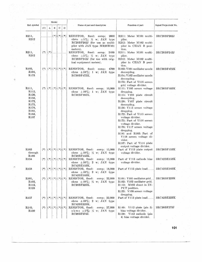
-------
Model Ref. symbol - Name of part and description Function of part Signal Oorps stock No. I
(U) ~_1='- 0 D -
R 211, ---- - -- (*) (*) ( *) RESISTOR, fixed: comp; 2000 R2Il: Meter MIOI multi- 3RC20BF202J R212 ohms ±5%; Yz w' , JAN type plier.
RC20BF202J (for use as multi- R2I2: :VIeter MI02 multi-plier with JAN type MR26W101 plier in CHAN B posi-meters). tion.
R 211, (*) ( *) - -- - -- - -- RESISTOR, fixed: comp; 2400 R211: Meter MI0I multi- 3RC20BF242J R2I2 ohms ±5%; Y2 w; JAN type plier.
RC20BF242J (for use with orig- R212: Meter M102 multi-inal equipment meters). plier in CHAN B posi-
(*)1(*) tion.
103, (*) ( *) ( *) RESISTOR, fixed: comp; 4700 R103: VIOl oscillator anode 3RC30BF472K R R104, ohms ±1O%; 1 w; JAN type decoupling. R173 RC30BF472K. RI04: VI02 oscillator anode
decoupling. Rl73: Part of V116 screen
grid voltage divider. R Ill, (*) ( *) ( *) ( *) (*) RESISTOR, fixed: comp; 10,000 RIll: V105 screen voltage 3RC30BFI03K
RIl5, ohms ±1O%; I w' , JAN type dropping. R120, RC30BF103K. R115: V103 plate circuit R156, decoupling. R172, R120: VI07 plate circuit RI75, decoupling. RI76, RI56: VIl3 screen voltage RI81,
I dropping.
R183, R172: Part of V115 screen RI97 voltage divider.
R175: Part of V1l6 screen I voltage divider.
R176: V1l7 screen voltage dropping.
R181 and R183: Part of V1l8 screen voltage di-
,
vider. R197: Part of V114 plate
output voltage divider. R 163 (*) ( *) ( *) ( *) ( *) RESISTOR, fixed: comp; 15,000 Part of V113 plate output 3RC20BF153K
through ohms ±10%; % w' , JAN type voltage divider. R166 RC20BF153K.
R 154 (*) ( *) ( *) ( *) ( *) RESISTOR, fixed: comp; 15,000 Part of VIl3 cathode bias 3RC42BE153K ohms ±10%; 2 ow; JAN type voltage divider. RC42BE153K.
R 158 (*) ( *) ( *) ( *) ( *) RESISTOR, fixed: comp; 18,000 Part of V113 plate load _____ 3RC42BE183K ohms ±1O%; 2 'v; JAN type RC42BE183K.
101, (*) ( *) ( *) ( *) (*) I
RESISTOR, fixed: comp; 22,000 R101: VIOl oscillator grid __ 3RC20BF223K Rl02, ohms ±10%; Yz w' JAN type R102: V102 oscillator grid. , R112, RC20BF223K. RIl2: Ml02 shunt in IN-
R
R123
I
PUT position. R123: Vl08 screen voltage
dropping. R 157 (*) ( *) ( *) ( *) ( *) RESISTOR, fixed: comp; 22,000 Part of VIl3 plate load _____ 3RC42BE223K
ohms ±10%; 2 w; JAN type RC42BE223K.
R 149, (*) ( *) ( *) ( *) ( *) RESISTOR, fixed: comp; 27,000 R149: V112 . plate (pin 5) 3RC20BF273J R150 ohms ±5%; % "w; JAN type bias voltage divider.
RC20BF273J. R150: V112 cathode (pin 4) bias voltage divider.
101
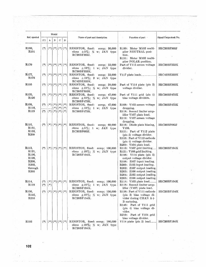
Model Ref. symbol Name of part and description Function of part - Signal dorps stock No.
(U) A B C D
--- - -R:189, (*) (*) (*) (*) ( *) RESISTOR, fixed: comp i 30,000 R189: Meter MI02 multi- 3RC20BF303J
R19l ohms ±5%i ~ Wi JAN type plier NEUTRAL·posi-RC20BF303J. tion.
/
R19l: Meter MI02 multi-plier POLAR position.
R170 (*) (*) (*) (*) ( *) RESISTOR, fixed: comp i 33,000 Part of V115 screen voltage 3RC30BF333K ohms ±10%i 1 W' , JAN type divider. RC30BF333K.
R177, (*) ( *) (*) (*) (*) RESISTOR, fixed: comp i 33,000 V117 plate loads __________ 3RC42BE333K RI78 ohms ±lO%i 2 W' , JAN type
RC42BE333K. RI95 (*) ( *) (*) ( *) ( *) RESISTOR, fixed: compi 39,000 Part of V1l4 plate (pin 2) 3RC20BF393K
ohms ±10%i ~ Wi JAN type voltage divider. RC20BF393K.
R125, (*) (*) (*) (*) (*) RESISTOR, fixed: compi 47,000 Part of Vll1 grid (pin 1) 3RC20BF473K R126 ohms ±10%i % w; JAN type bias voltage dividers.
RC20BF473K. \
R108, (*) ( *) (*) ( *) ( *) RESISTOR, fixed: compi 47,000 R108: V103 screen voltage 3RC30BF473K R118, ---- --- (*) ( *) ( *) ohms ±10%i 1 W' , JAN type dropping. R119 (*) (*) (*) ( *) ( *) RC30BF473K. Rl18: Second limiter amp-
lifier V107 plate load. R119: V107 screen voltage
dropping. Rl16, (*) (*) (*) (*) (*) RESISTOR, fixed: compi 68,000 R116: Diode plate biasing, 3RC30BF683J
R151, ohms ±5%i I W' , JAN type V106. R153, RC30BF683J. R151: Part of V112 plate R209 (pin 5) voltage divider.
R153: Part of Vl12 cathode (pin 4) voltage divider.
R209: V104 plate load. R113, (*) (*) (*) ( *) (*) RESISTOR, fixed: comp; 100,000 R113: V107 grid limiting ___ 3RC20BFI04K
R121, ohms ±10%; ~ Wi JAN type R121: VI08 grid limiting. RI96, RC20BFI04K. R196: V114 plate (pin 5)
. RI98, output voltage divider . R200, RI98: Z107 input loading. R202, R200: ZI05 input loading. through R202: Z107 output loading. R205 R203: ZI08 output loading.
R204: Z105 output loading. R205: ZI06 output loading.
R114, (*) (*) (*) ( *) (*) RESISTOR, fixed: comp i 100,000 RI14: VI03 plate load _____ 3RC30BFI04K Rl18 (*) (*) ohms ±IO%; I W' JAN type Rl18: Second limiter amp-,
~c.; .. >
RC30BF104K. lifier (V107) plate load. R136, (*) (*) (*) ( *) (*) RESISTOR, fixed: comp; 150,000 R136: Part of V111 cathode 3RC20BF154K
R146; ohms ±10%i ~ w; JAN type (pin 3) bias voltage di-R210 RC20BFI54K. vider during CHAN A +
B metering. R146: Part of Vlli grid
(pin 4) bias voltage di-vider.
R210: Part of VI04 grid . - bias voltage divider. R193 (*) ( *) (*) (*) (*) RESISTOR, fixed: compi 180,000 V114 plate (pin 2) load ____ 3RC20BF184K
ohms ±10%i ~ Wi JAN type RC20BF184K.
102
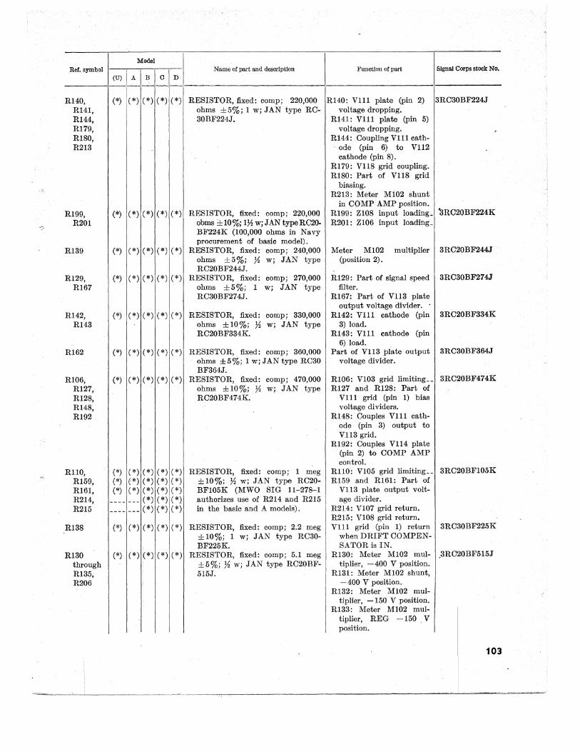
Model Name of part and desorlptlon Function of part Signal Corps stock No.
Ref. symbol I I _________ I_(_U_) ~_~~_D __ I--__ ------------------------I----------------------I-------------R140,
R141, R144, R179, R180, R213
Rl99, R201
R139
R129, R167
R142, R143
R162
R106, R127, R128, R148, R192
RllO, R159, R161, R214, R215
R138
R130 through R135, R206
(*) (*) (*) (*) (*) RESISTOR, fixed: comp; 220,000 ohms ±5%i 1 wi JAN type RC-30BF224J.
(*) (*) (*) (*) (*) RESISTOR, fixed: comp; 220,000 obms±10%i 17'2 wi JAN type RC20-BF224K (100,000 ohms in Navy procuremen t of basic model).
(*) (*) (*) (*) (*) RESISTOR, fixed: comp; 240,000 ohms ±5%; 7'2 w; JAN type RC20BF244J.
(*) (*) (*) (*) (*) RESISTOR, fixed: comp; 270,000 ohms ±5%; 1 wi JAN type RC30BF274J.
(*) (*) (*) (*) (*) RESISTOR, fixed: compi 330,000 ohms ±10%i 7'2 Wi JAN type RC20BF334K.
(*) (*) (*) (*) (*) RESISTOR, fixed: comp; 360,000 ohms ±5%; 1 w;JANtype RC30 BF364J.
(*) (*) (*) (*) (*) RESISTOR, fixed: comp; 470,000 ohms ±10%; 7'2 w; JAN type RC20BF474K.
(*) (*) (*) (*) (*) (*) (*) (*) (*) (*) (*) (*) (*) (*) (*)
---- --- (*) (*) (*) ---- --- (*) (*) (*)
(*) (*) (*) (*) (*)
(*) (*) (*) (*) (*)
RESISTOR, fixed: comp; 1 meg ± 10%; ~ w; JAN type RC20-BF105K (MWO SIG 11-278-1 authorizes use of R214 and R215 in the basic and A models).
RESISTOR, fixed: comp; 2.2 meg ± 10%; 1 w; JAN type RC30-BF225K.
RESISTOR, fixed: comp; 5.1 meg ±5%; ~ w; JAN type RC20BF-515J.
R140: Vll1 plate (pin 2) 3RC30BF224J voltage dropping.
R141: VIll plate (pin 5) voltage dropping.
R144: Coupling V111 cathode (pin 6) to V1l2 cathode (pin 8).
R179: V118 grid coupling. R180: Part of V118 grid
biasing. R213: Meter M102 shunt
in COMP AMP position. R199: Z108 input loading_ '3RC20BF224K R201: Z106 input loading_
Meter M102 multiplier 3RC20BF244J (position 2).
R129: Part of signal speed 3RC30BF274J filter.
R167: Part of VIl3 plate output voltage divider.
R142: Vlll cathode (pin 3RC20BF334K 3) load.
R143: V111 cathode (pin 6) load.
Part of V113 plate output 3RC30BF364J voltage divider.
R106: V103 grid limiting __ 3RC20BF474K R127 and R128: Part of
V1l1 grid (pin 1) bias voltage dividers.
R148: Couples Vll1 cathode (pin 3) output to V1l3 grid.
R192: Couples V1l4 plate (pin 2) to COMP AMP control.
Rll0: V105 grid limiting __ 3RC20BFI05K RI59 and R161: Part of
V1l3 plate output volt-age divider.
R214: V107 grid return. R215: V108 grid return. Vll1 grid (pin 1) return 3RC30BF225K
when DRIFT COMPEN-SATOR is IN.
R130: Meter M102 mul- .3RC20BF515J tiplier, -400 V position.
R131: Meter M102 shunt, -400 V position.
R132: Meter MI02 multiplier, -150 V position.
R133: Meter MI02 mul- I
tiplier, REG -150 V position.
103
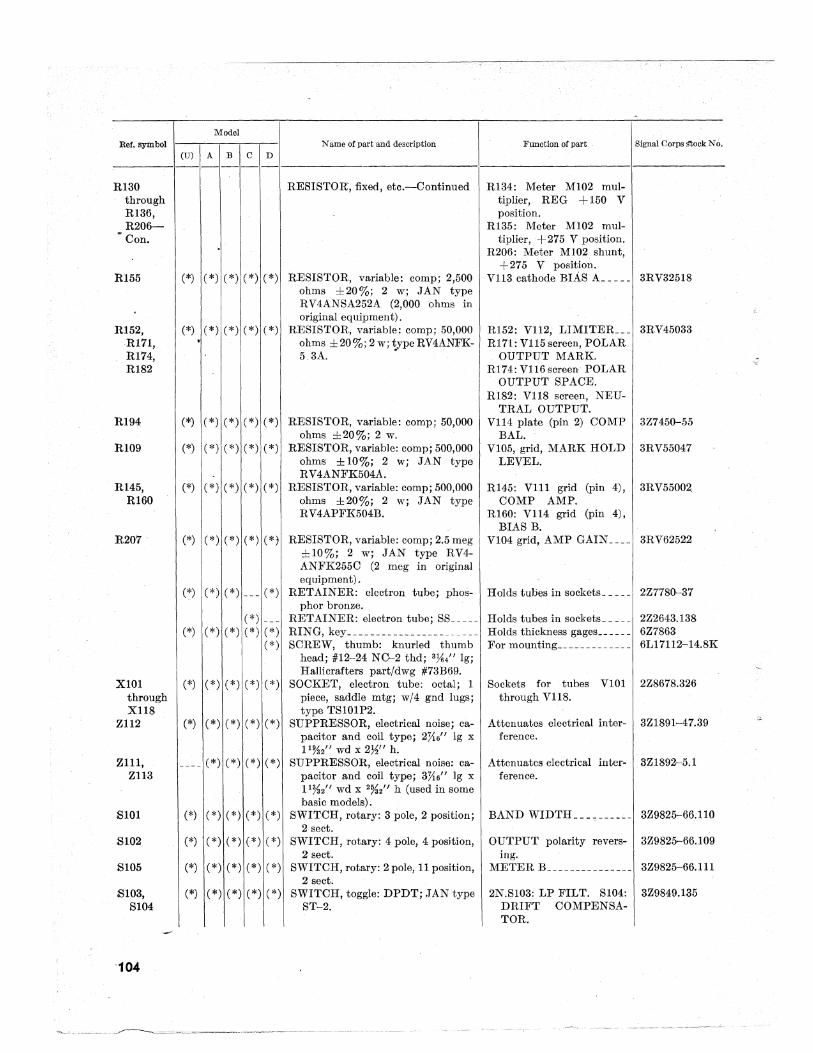
Model Ref. symbol Name of part and description Function of part Signal Corps !!'tock No.
(U)ABCD -----1---1--------1----------------1------------1----------
R130 through R136, R206-
• Con.
R155
Rl52, R171, R174, R182
R194
R109
R145, R160
R207
X101 through X1l8
Z112
Z111, Z1l3
S101
8102
8105
8103, S104
104
(*) (*) (*) (*) (*)
(*) (*) (*) (*) (*)
(*) (*) (*) ( *) (*)
I (*) (*) ( *) (*). (*)
(*) (*) ( *) ( *) ( *)
(*) (*) ( *) (*) (*)
(*) ( *) (*) - -- (*)
(*) ---(*) (*) ( *) (*) (*)
(*)
(*) ( *) (*) (*) ( *)
(*) (*) ( *) (*) ( *)
- - -- (*) ( *) (*) ( *)
(*) ( *) ( *) ( *) ( *)
(*) ( *) ( *) (*) ( *)
(*) (*) (*) (*) ( *)
(*) ( *) ( *) (*) ( *)
I
RESISTOR, fixed, etc.-Continued R134: Meter M102 mul-
RESISTOR, variable: comp; 2,500 ohms ±20%; 2 w; .TAN type RV4ANSA252A (2,000 ohms in original equipment).
RESISTOR, variable: comp; 50,000 ohms ±20%;2w;typeRV4ANFK-5 3A. •
RESISTOR, variable: comp; 50,000 ohms ±20%; 2 w.
RESISTOR, variable: comp; 500,000 ohms ± 10%; 2 w; JAN type RV4ANFK504A.
RESISTOR, variable: camp; 500,000 ohms ±20%; 2 w; JAN type RV 4APFK504B.
RESISTOR, variable: comp; 2.5 meg ± 10%; 2 w; JAN type RV4-ANFK255C (2 meg in original equipment) .
RET AINER: electron tube; phos-phor bronze.
RETAINER: electron tube; SS ____ _ RING, key ______________________ _
SCREW, thumb: knurled thumb head; #12-24 NC-2 thd; 3H4/1 19; Hallicrafters part/dwg #73B69.
SOCKET, electron tube: octal; 1 piece, saddle mtg; w/4 gnd lugs; type TS10lP2.
SUPPRESSOR, electrical noise; capacitor and coil type; 2%6/1 19 x 11%2/1 wd X 2%" h.
SUPPRESSOR, electrical noise: capacitor and coil type; 3%6/1 19 X
11%2/1 wd X 2%2/1 h (used in some basic models).
SWITCH, rotary: 3 pole, 2 position; 2 sect.
SWITCH, rotary: 4 pole, 4 position, 2 sect.
SWITCH, rotary: 2 pole, 11 position, 2 sect.
SWITCH, toggle: DPDT; .TAN type ST-2.
tiplier, REG + 150 V position.
R135: Meter M102 multiplier, +275 V position.
R206: Meter MI02 shunt, +275 V position.
V113 cathode BIAs L ____ 3RV32518
R152: V112, LIMITER ___ 3RV45033 RI71: VI15 screen, POLAR
OUTPUT MARK. R174: V116screen POLAR
OUTPUT SPACE. R182: V1l8 screen, NEU
TRAL OUTPUT. V114 plate (pin 2) COMP
BAL. VI05, grid, MARK HOLD
LEVEL.
3Z7450-55
3RV55047
R145: Vll1 grid (pin 4), 3RV55002. COMP AMP.
R160: V114 grid (pin 4), BIAS B.
VI04 grid, AMP GAIN ____ 3RV62522
Holds tubes in sockets_ _ _ _ _ 2Z7780--37
Holds tubes in sockets _____ 2Z2643.138 Holds thickness gages__ _ _ _ _ 6Z7863 For mounting _____________ 6Ll7112-14.8K
Sockets for tubes VIOl 12Z8678.326 through V1l8.
Attenuates electrical inter- 3Z189I-47.39 ference.
Attenuates electrical inter- 3Z1892-5.1 ference.
BAND WIDTH __________ 3Z9825-66.1l0
OUTPUT polarity revers- 3Z9825-66.109 ing.
METER B_ _ _ _ _ _ _ _ _ _ _ _ _ _ _ 3Z9825-66.111
2N.SI03: LP FILT. S104: 3Z9S49.135 DRIFT COMPENSA-TOR.
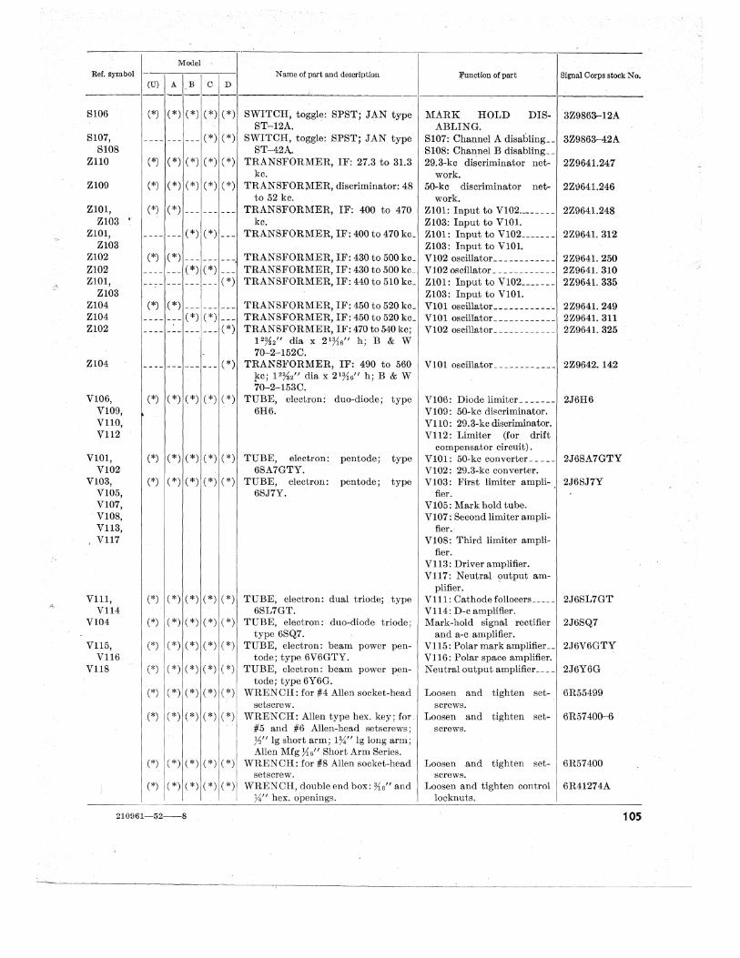
MOdel , Ref. symbol N arne of part and description ~unction of part Signal Corps stock No.
(U)A.BCD -----1--------1--------''----,------1------,-----,1-------
S106
Sl07, S108
ZllO
Z109
ZlOl, Z103 '
Z101, Z103
ZI02 Z102, ZI01,
Z103 ZI04 Z104 ZI02
Zl04
V106, VI09, VllO, Vll2
VIOl, V102
V103, V105, V107,
, V108, Vll3,
, Vll7
V1ll, Vll4
V104
V1l5, Vll6
V118
(*) (*) (*) (*) (*) SWITCH, toggle: SPST; JAN type ST-12A.' ,
---- --- - __ (*) (*) SWITCH, toggle: SPST; JAN, type ST-42A.
(*) (*) (*) (*) (*) TRANSFORMER, IF: 27.3 to 31.3 kc.
(*) (*) (*) (*) (*) TRANSFORMER, discriminator: 48 to 52 kc.
(*) (*) _________ TRANSFORMER, IF: 400 to 470 kc.
_______ (*) (*) ___ TRANSFORMER,IF:400to470kc_
(*) (*) _________ TRANSFORMER,IF:430to500kc_ _______ (*) (*) ___ TRANSFORMER,IF:430to500kc_
_________ (*) TRANSFORMER, IF: 440 to 510kc_
(*) (*) _________ TRANSFORMER,IF:450to520kc_ _______ (*) (*) ___ TRANSFORMER,IF:450to520kc_
(*) TRANSFORMER, IF: 470 to 540 kc; 12%2" dia x 2 1%6" h; B & W 70-2-152C.
___________ .. _ (*) TRANSFORMER, IF: 490 to 560 ~c; 12%2" dia x 2 1%6" h; B & W 70-2-153C.
(*) (*) (*) (*) (*) TUBE, electron: duo-diode; type 6H6.
(*) (*) (*) (*) (*) TUBE, electron: pentode; type 6SA7GTY.
(*) (*) (*) (*) (*) TUBE, electron: pentode; type 6SJ7Y.
(*) (*) (*) (*) (*) TUBE, electron: dual triode; type 6SL7GT.
(*) (*) (*) (*) (*) TUBE, electron: duo-diode triode; type 6SQ7.
(*) (*) (*) (*) (*') TUBE, electron: beam power pentode; type 6V6GTY.
(*) (*) (*) (*) (*) TUBE, electron: beam power pen-tode; type 6Y6G. '
(*) (*) (*) (*) (*) WRENCH: for #4 Allen socket-head
MARK HOLD DIS- 3Z9863-12A ABLING.
S107: Channel A disabling __ 3Z9863-42A Sl08: Channel B disabling __ 29.3-kc discriminator net- 2Z9641.247
work. 50-kc discriminator net- 2Z~641.246
work. Z101: Input to V102. _______ 2Z9641.248 Z103: Input to VIOL ZIOI: Input to VI02 _______ 2Z9641. 312 Z103: Input to VIOL VI02oscillator ____________ 2Z9641. 250 V102 oscillator _ _ _ _ _ _ _ _ _ _ _ _ 2Z964l. 310 ZIOI: Input to V102____ _ _ _ 2Z9641. 335 Z103: Input to VIOL VlOloscillator ____________ 2Z964l. 249 VlOloscilIator ____________ 2Z964l. 311 V102 oscillator _ _ _ _ _ _ _ _ _ _ _ _ 2Z964l. 325
VIOl oscillator _ _ _ _ _ _ _ _ _ __ _ 2Z9642. 142
VI06: Diode limiter _______ 2J6H6 Vl09: 50-kc discriminator. VllO: 29.3-kc discriminator. V1l2: Limiter (for drift
compensator circuit). VIOl: 50-kc converter _____ 2J6SA7GTY VI02: 29.3-kc converter. Vl03: First limiter ampli-. 2J6SJ7Y
fier. V105: Mark hold tube. VI07: Second limiter ampli
fier. V108: Third limiter ampli
fier. Vll3: Driver amplifier. V1l7: Neutral output am-
plifier. ' VllI: Cathodefolloeers _____ 2J6SL7GT Vll4: D-c amplifier. Mark-hold signa.l rectifier 2J6SQ7
and a-c amplifier. V1l5: Polar mark amplifier __ 2J6V6GTY Vll6: Polar space amplifier. Neutral output amplifier___ _ 2J6Y6G
Loosen and tighten set- 6R55499 setscrew. screws.
(*) (*) (*) (*) (*) WRENCH: Allen type hex. key; for, Loosen and tighten set- 6R57400-6 #5 and #6 Allen-head setscrews; screws. ~~" 19 short arm; 1%" 19 long arm; Allen Mfg }{6" Short Arm Series. '
(*) (*) (*) (*) (*) WRENCH: for #8 Allen socket-head Loosen and tighten set- 6R57400 setscrew.
(*) (*) (*) (*) (*) WRENCH,doubleendbox:%6"and W' hex. openings.
screws,. Loosen and tighten control 6R41274A
locknuts.
210961-52-8 105
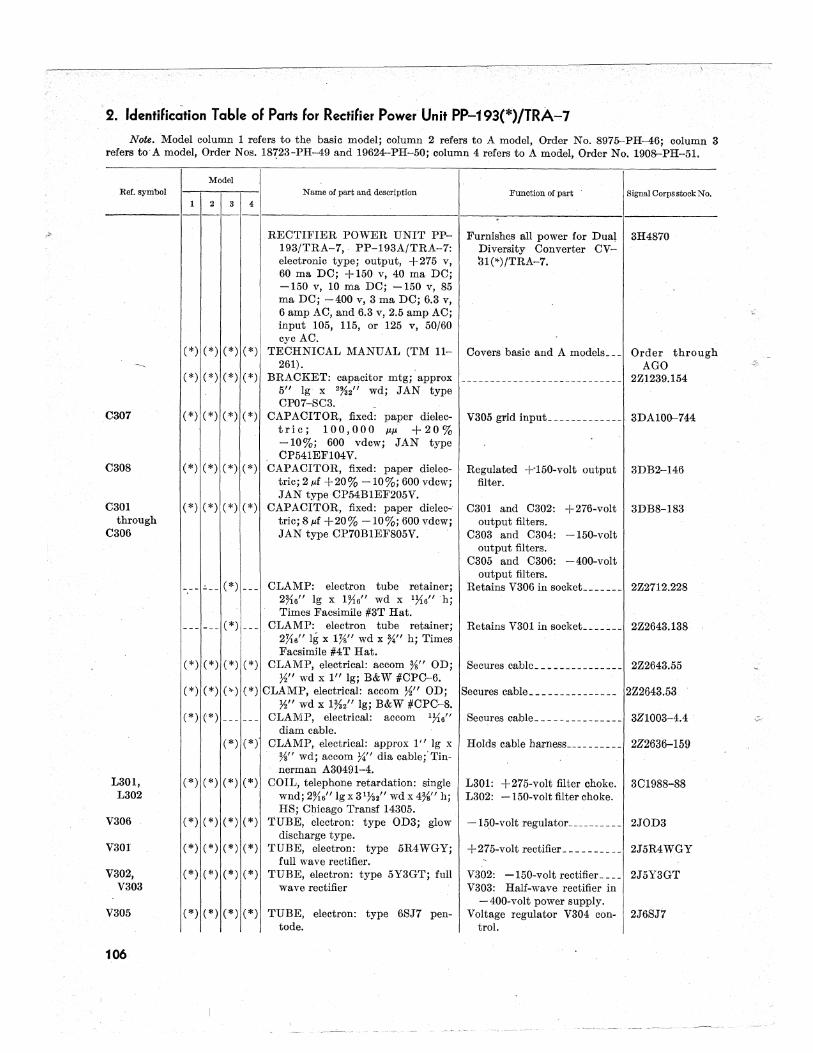
2. Identification Table of Parts for Rectifier Power Unit PP-193(*)/TRA-7
Note. Model column 1 refers to the basic model; column 2 refers to A model, Order No. 8975-PH-46; column 3 refers to A model, Order Nos. 18723-PH-49 and 19624--PH-50; column 4 refers to A model, Order No. 190&-PH-51.
Model Ref. synibol
1 2 3 4
(*) (*) (*) (*)
(*) (*) (*) (*)
Name of part and description
RECTIFIER POWER UNIT PP-193/TRA-7" PP-193A/TRA-7: electronic type; output, +275 v, 60 ma DC; + 150 v, 40 ma DC; -150 v, 10 ma DC; -150 v, 85 ma DC; -400 v, 3 ma DC; 6.3 v, 6 amp AC, and 6.3 v, 2.5 amp AC; input 105, 115, or 125 v, 50/60 cyc AC.
TECHNICAL MANUAL (TM 11-261).
BRACKET: capacitor mtg; approx 5" Ig x 2%2" wd; JAN type CP07-SC3.
Function of part Signal Corps stock No.
Furnishes all power for Dual 3H4870 Diversity Converter CV-31 (*) /TRA-7.
Covers basic and A models_ _ _ Order through AGO
___ _ _ __ _ _ _ _ _ _ __ __ ____ __ ___ _ _ 2Z1239.154
C307 (*) (*) (*) (*) CAPACITOR, fixed: paper dielec- V305 grid inpuL ____________ 3DA10o-744
C308
C301 through
C306
L301, L302
V306
V301
V302, V303
V305
106
t ric; I 0 0 , 0 0 0 /L/L + 2 0 % -10%; 600 vdcw; JAN type CP541EF104V.
(*) (*) (*) (*) CAPACITOR, fixed: paper dielectric; 2 /Lf +20% -10%; 600 vdcw; JAN type CP54BlEF205V.
(*) (*) (*) ( *) CAPACITOR, fixed: paper dielectric; 8 /Lf +20% -10%; 600 vdcw; JAN type CP70B1EF805V.
___ (*) ___ CLAMP: electron tube retainer; 2%6" 19 x 1%6" wd x 1X6"h; Times Facsimile #3T Hat.
___ - __ (*) _ _ _ CLAMP: electron tube retainer; 2~6" Ig x 1Ys" wd x W' h; Times Facsimile #4 THat.
(*) (*) (*) (*) CLAMP, electrical: accom %" OD; W' wd x I" 19j B&W #CPC-6.
(*) (*) (,,) (*) CLAMP, electrical: accom W' OD; W' wd x 1%2" Ig; B&W #CPC-8.
(*) (*) ______ CLAMP, electrical: accom 1X6"
(*) ( *)
(*) (*)
(*) (*)
(*) (*)
(*) (*)
diam cable. (*) (*Y CLAMP, electrical: approx Ii! 19 x
%" wd; accom W' dia cable;' Tinnerman A30491-4.
(*) (*) COIL, telephone retardation: single wnd; 2%6" 19 x 3 17'32" wd x 4%" h; HS; Chicago Transf 14305.
(*) (*) TUBE, electron: type OD3; glow discharge type.
( *) (*) TUBE, electron: type 5R4WGY; full wave rectifier.
(*) (*) TUBE, electron: type 5Y3GT; full wave rectifier
(*) (*) TUBE, electron: type 6SJ7 pen-tode.
Regulated +150-volt output filter.
C301 and C302: +276-volt output filters.
C303 and C304: -150-volt output filters.
C305 and C306: -400-volt output filters.
3DB2-146
3DB8-183
Retains V306 in socket _______ 2Z27I2.228
Retains V301 in sockeL _ _ _ _ _ _ 2Z2643.I38
Secures cable_ _ _ _ _ _ _ _ _ _ _ _ _ _ _ 2Z2643.55
Secures cable_ _ _ _ __ _ _ _ ___ ___ 2Z2643.53
Secures cable _______________ 3Z1003-4.4'
Holds cable harness __________ 2Z2636-159
L301: +275-volt filter choke. 301988-88 L302: -I50-volt filter choke,
-I50-volt regulator __________ 2JOD3
+ 275-volt rectifier __________ 2J5R4WGY "
V302: -150-volt rectifier ____ 2J5Y3GT V303: Half-wave rectifier in
-400-volt power supply. Voltage regulator V304 con- 2J6SJ7
trol.
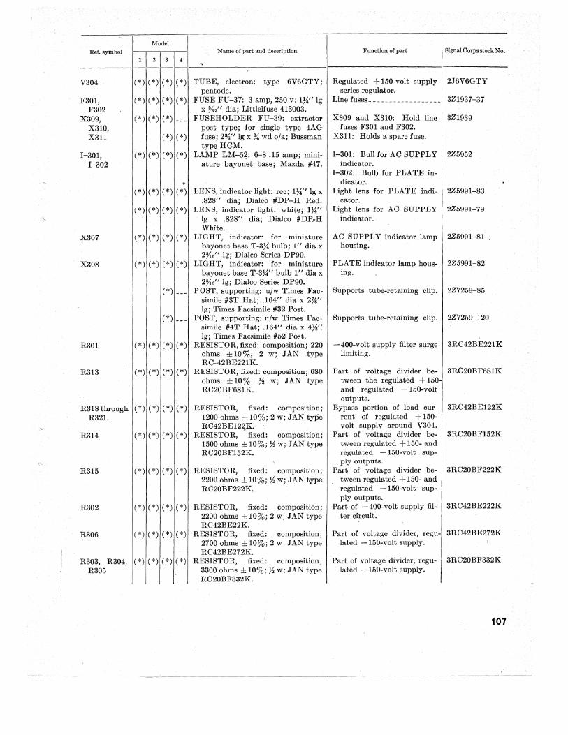
Ref. symbol
V304
F301, F302
X309, X310, X311
1-301, 1-302
X307
X308
R301
Model. Name of part and description
1 2 3 4
(*) (*) (*) (*) TUBE, electron: type 6V6GTY; pentode.
(*) (*) (*) (*) FUSE FU-37: 3 amp, 250 v; IX" 19 X %2" dia; Littlelfuse 413003.
(*) (*) (*) ___ F~USEHOLDER FU-39: extractor post type; for single type 4AG
(*) (*) fuse; 2%" 19 x % wd o/a; Bussman t:ype HCM.
(*) (*) (*) (*) LAMP LM-5~: 6-8.15 amp; miniature bayonet base; Mazda #47.
(*) (*) (*) (*)
(*) (*) (*) (*)
LENS, indicator light: rec; IX" 19 x .828" dia; Dialco #DP-H Red.
LENS, indicator light: white; IX" 19 x .828" dia; Dialco #DP,.H White.
(*) (*) (*) (*) LIGHT, indicator: for miniature bayonet base T-3X bulb; 1" dia x 2%6" 19; Dialco Series DP90.
(*) (*) (*) (*) LIGHT, indicator: for miniature bayonet base T-3X" bulb 1" dia x 2%6" 19; Dialco Series DP90.
(*) ___ POST, supporting: u/w Times Fac-simile #3T Hat; .164" dia x 2%" 19; Times Facsimile #32 Post.
(*) ___ POST, supporting: u/w Times Fac-simile #4T Hat; .164" dia x 4W~ 19; Times Facsimile #52 Post. ~
(*) (*) (*) (*) RESISTOR, fixed: composition; 220 ohms ±10%j 2 w; JAN .type RC-42BE221K. .
R313 (*) (*) (*) (*) RESISTOR, fixed: composition; 680
R318through (*) (*) (*) (*) R321.
R314 (*) (*) (*) (*)
ohIIis ± 10%; ~ w; JAN type RC20BF681K.
RESISTOR, fixed: composition; 1200 ohms ± 10%; 2 w; JAN type RC42BE12~K.
RESISTOR, fixed: composition; 1500 ohms ± 10%; ~ w; JAN type RC20BF152K.
R315 (*) (*) (*) (*) RESISTOR, fixed: composition;
R302 (*) (*) (*) (*)
R306 (*) (*) (*) (*)
R303, R304, (*) (*) (*) (*) R305
2200 ohms ± 10%; ~ w; JAN type RC20BF222K.
RESISTOR, fixed: composition; 2200 ohms ± 10%; 2 w; JAN type RC42BE22K.
RESISTOR, fixed: composition; 2'700 ohms ± 10%; 2 w; JAN type RC42BE272K.
RESISTOR, fixed: composition; 3300 ohms ± 10%; ~ w; JAN type RC20BF332K.
Function of part Signal Corps stock No.
Regulated + 150-volt supply 2J6V6GTY series regulator.
Line fuses __________________ 3Z1937-37
X309 and X310: Hold line 3Z1939 fuses F301 and F302.
X311: Holds a spare fuse.
1-301: Bull for AC SUPPLY 2Z5952 indicator.
1-302: Bulb for PLATE indicator.
Light lens for PLATE indicator.
Light lens for AC SUPPLY indicator.
2Z5991-83
2Z5991-79
AC SUPPLY indicator lamp 2Z5991-81 housing.
PLATE indicator lamp hous- 2Z5991.,..82 ing.
Supports tube-retaining clip. 2Z7259-S5
Supports tube-retaining clip., 2Z7259-120
-400-volt supply filter surge 3RC42BE221K limiting.
Part of voltage divider be- 3RC20BF681K tween the regulated + 150-and regulated -150-volt outputs.
Bypass portion of load cur- 3RC42BE122K rent of regulated + 150-volt supply around V304.
Part of voltage divider be- 3RC20BF152K tween regulated + 150- and regulated -150-volt sup-ply outputs.
Part of voltage divider be- 3RC20BF222K tween regulated + 150- and regulated -150-volt sup-ply outputs.
Part of -400-volt supply fil- 3RC42BE222K ter circuit.
: Part of voltage divider, regu- 3RC42BE272K lated -150-volt supply. )
Part of voltage divider, regu- 3RC20BF332K lated -150-volt supply.
107
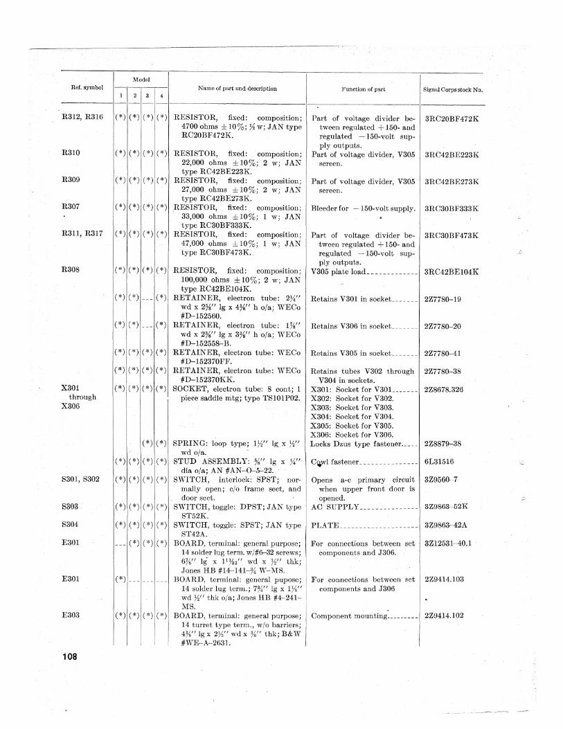
Model Ref. symbol Name of part and description Function of part Signal Corps stock No.
1 2 3 4
----------��---------�--------------------------�---------~----~----I------------
R312, R316
R310
R309
R307
R311, R317
R30S
X301 through
X306
S30I, S302
8303,
S304
E301
E301
E303
108
(*) (*) (*) (*) RESISrOR, fixed: composition; 4700 'ohms ± 10%; % w; JAN type RC20BF472K.
(*) (*) (*) (*)
(*) (*) (*) (*)
(*) (*) (*) (*)
(*) (*) (*) (*)
(*) (*) (*) (*)
(*) (*) --- (*)
(*) (*) --- (*)
RESISTOR, fixed: composition; 22,000 ohms ± 10%; 2 w; JAN type RC42BE223K.
RESISTOR, fixed: composition; 27,000 ohms ± 10%; 2 w; JAN type RC42BE273K.
RESISTOR, fixed: composition; , 33,000 ohms ± 10%; 1 w; JAN
type RC30BF333K. RESISTOR, fixed: composition;
47,000 ohms ±10%; 1 w; JAN type RC30BF473K..
RESISTOR, fixed: composition; 100,000 ohms ± 10%; 2 w; JAN type RC42BE104K.
RETAINER, electron tube: 2)4" wd x 2%" 19 x 4%" h o/a; WECo #D-I52560.
RETAINER, electron tube: 1%" wd x 2%" 19 x 3%" h o/a; WECo #D-152558--B.
Part of voltage divider be- 3RC20BF472K tween regulated + 150- and regulated -150-volt sup-ply outputs.
Part of voltage divider, V305 3RC42BE223K screen.
Part of voltage divider, V305 3RC42BE273K screen.
Bleeder for -I50-volt supply. 3RC30BF333K • I
Part of voltage divider be- 3RC30BF473K tween regulated + 150- and regulated -150-volt sup-ply outputs.
V305 platE) load_ _ _ _ _ _ _ _ _ _ _ _ _ 3RC42BE104K
Retains V301 in sockeL ______ 2Z7780-19
Retains V306 in socket _______ 2Z7780-20
(*) (*) (*) (*) RETAINER, electron tube: WECo Retains V305 in sockek ______ 2Z7780-41 #D-152370FF.
(*) (-*) (*) (*) RETAINER, electron tube: WECo #D-152370KK.
(*) (*) (*) (*) SOCKET, electron tube: 8 conti I piece saddle mtg; type TSI01P02.
(*) (n SPRING: loop type; 1%" 19. x %"
(*) (*) (*) (*)
(*) (*) (*) (*)
(*) (*) (*) (*)
(*) (*) (*) (*)
--- (*) (*) (*)
(*) --- --- ---
(*) (*) (*) (*)
wd o/a. STUD ASSEMBLY: %" 19 x y.",
dia 0/8.) AN #AN-O"':5:c.22. SWITCH, interlock: SPST; nor
mally open; c/o frame sect, and door sect.
SWITCH, toggle: DPST; JAN type ST52K.
SWITCH, toggle: SPST; JAN type ST42A.
BOARD, terminal: general purpose; 14 solder lug term. w/#6-32 screws; 6%" 19 x J17b" wd x W' thk; Jones HB #14-141-% W-MS.
BOARD, terminal: general pupose; 14 solder lug term.; 7%" 19 x lW' wd %" thk 0/8.; Jones HB #4-241-MS.
BOARD, terminal: general purpose; 14 turret type term., w/o barriers; 4%" 19 x 2W' wd x %" thk; B&W #WE-A-2631.
Retains tubes V302 through 2Z7780-38 V304 in sockets.
X301: Socket for V30L ______ 2Z8678.326 X302: Socket for V302. X303: Socket for V303. X304: Socket for V304. X305: Socket for V305. X306: Socket for V306. Locks Dzus type fastener. ____ 2Z8879-38
C~wl fasteneL ______________ 6L31516
Opens a-c primary circuit 3Z9560-7 when upper front door is opened.
AC SUPPLY ____ _ _ __ _ _ _____ 3Z9863-52K
PLATE- __ ________ _ _ _ _ _ _ __ _ 3Z9863-42A
For connections between set 3Z12531-40.1 components and J306.
For connections between set 2Z9414.103 components and J306
-Componentmounting._______ _ 2Z9414.102
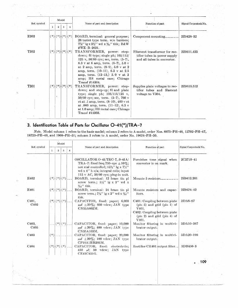
.-
~
-.
..~
Model Ref. symbol Name of part and description Function of part Signal Corps stock No.
1 2 3 4
----------�---------�-------------~-----------I-----~--------------I,------------
E302
T302
TaO!
(*) (*) (*) (*) BOARD, terminal: general purpose; 28 turret type term. w/o barriers; 7W'lgx2W'wd X %211 thk; B&W #WE-B-2621.
(*) (*) (*) (*) TRANSFORMER, power: step~
down; fil tYPe; single ph; 105/115/ 125 v, 50/60 cyc; sec, term. (5-7), 6.3 v at 6 amp, term. (6-7), 5.0 v at 2 amp, term. (8-9), 5.0 v at 2 amp, term. (10--11), 6.3 v at 2.5 amp, term. (12-13,) 5.0 v at 2 amp; HS metal case; Chicago Transf #14304.
(*) (*) (*) (*) TRANSFORMER, power: stepdown; and step-up; filand plate type; sirigle ph; 105/115/125 v, 50/60 cyc; sec, term. (5-7),760 v ct at.l amp, term. (8-10),460 v ct at .060 amp, term. (11-12), 6.3 v at 1.0 amp; HS metal case; Chicago Transf #14303.
Component mounting. ________ 2Z9428-32
Filament transformer for rec- 2Z9611.423 tifier tubes in power supply and all tubes in converter.
Supplies plate voltages to rec- 2Z9613.512 tifier tubes and filament voltage to V304.
3. Identification Table of Parts for Oscillator 0-41 (*)/TRA-7 Note. Model column 1 refers to the basie mo:lel; column 2 refers to A model, order Nos. 8975-PH-46, 12702-PH-47,
18723-PH-49, and 1908-PH-51; column 3 refers to A model, order No. 19624-PH-50.
Model Ref. symbol Name of part and description Function fpart Signal Corps stock No.
1 2 3 ·4
----
OSCILLATOR 0-41/TRC-7, .0-41A/ Furnishes tone signal when 2C271Q--41 TRA-7: fixed freq 75Q--cps ± 10%; converter is 0 mark.
,
not xtal controlled; 15~1I 19 x 7%11 wd X 4" h o/a; integral coils; input 115 v AC, 50/60 cyc; plug-in unit.
E402 (*) ( *) (*) - -- BOARD, terminal: 12 brass tin pi . Mounts 5 resistc rs ___________ 2Z9412.201 screw term.; 5%" 19 x 3" wd X %2" thk.
E401 ( *) ( *) ( *) --- BOARD, terminal: 24 brass tin pi Mounts resistor and capac- 2Z9424-42 screw term.; 7%" 19 x 2" wd X %2" itors. thk.
C401, ( *) ( *) (*) - -- CAPACITOR, fixed: paper; 6,000 C401: Coupling etween plate 3DA6-p7 C402 ppf ±20%; 660 vdcw; JAN type (pin 5) and g id (pin 1) of
CN35A602M. V401. C402:Coupling etween plate
(pin 2) and g id (pin 4) of V401.
C403,. - -- (*) ( *) --- CAPACITOR, fixed: paper; 10,000 Monitor filterin in multivi- 3DAIQ--367 C405 ppf ±20%; 400 vdcw; JAN type brator output.
CN35AI03M. C403 (*) - -- - -- --- CAPACITOR, fixed: paper; 20,000 Monitor filterin in multivi- 3DA2Q--199
ppf ±20%; 100 vdcw; JAN type brator output. CPI6AlHB203M.
C404 ( *) ( *) ( *) - -- CAPACITOR, fixed: electrolytic; Rectifier CR40l putput filter __ 3DB45Q--a 450 pf; 50 vdcw; JAN type
I CE41C451G.
. 109
, I
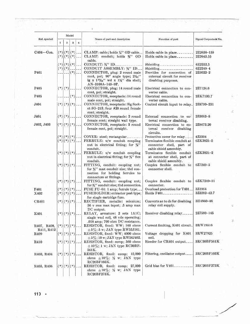
Ref. symbol
C404-Con.
P401
P405
1'405
J404
J401
J402, J403
F401 X402
CR401
Model
1 2 3 4
(*) (*) (*) --(*) (*) (*) ---
(*) (*) (*) --(*) (*) --- ----- --- (*) ---
(*) (*) --- --
--- --- (*) --
(*) (*) (*) ---
(*) (*) --- --
(*) (*) (*) ---
(*) (*) (*Y --(*) (*) (*) ---
(*) (*) (*) ---
(*) (*) (*) ---
(*) (*) (*) --
(*) (*) en --(*) (*) (~)
I
(*) (*) (*) ---.
K401 (*) (*) (*) __ _
R407, R408, (*) (*) (*) --R411, R412
R409 (*) (*) (*) __ _
R410 (*) (*) (*) __ _
R403, R404 (*) (*) (*) __ _
R405, R406 (*) (*) (*) __ _
110
Name of part and description
CLAMP: cablej'holds~" OD cable __ CLAMP,: conduitj holds %" OD
cable. CONDUIT: %" ID _______________ _ CONDUIT ASSEMBLY: %" ID __ _ CONNECTOR, plug: 2 round male
cont, polj 90° angle typej 2%2" 19 X }2%2" wd x IYs" dia shellj AN-3108A-14S-9P. .
CONNECTDR, plug: 14 round male cont, pol; straight.
CONNECTOR, receptacle: 14 round male cont, pol; straight.
CONNECTOR, receptacle: Sig Socket S0-213; four #20 round female conti straight.
CONNECTOR, receptacle: 2 round female cont; straight wall type.
CONNECTOR, receptacle: 3 round female cont, pol; straight.
COVER:steeli rectangular-, _______ _ FERRULE;. u/w conduit coupling
nut in electrical fittingi fol' %" conduit.
FERRULE: u/w conduit coupling nut in electrical fitting; for W' flex conduit.
FITTING, conduit: coupling nut; for %" max conduit· size; thd connection for holding ferrules to connectors or fittings.
FITTING, conduit: coupling nut; for W' conduit size; thd connection.
FUSE FU-64: I amp; ferrule type __ _ FUSEHOLDER:.extractor post type;
for single cartridge fuse. RECTIFIER, metallic: selenium;
36 v rms max input; .5 amp max DC output.
RELAY, armature: 2 sets lAIC; single wnd coil, 48 vdc operating; .018 amp; 700 'ohm DC resistance.
RESISTOR, fixed: WW; l60'ohms ±5%i 5 w; JAN type RW55J161.
RESISTOR, fixed: WW; 4000 ohms ±5%; lOw; JAN type RW56J402.
RESISTOR, fixed: comp; 560 ohms ± 10%; I w; JAN type RC30BF
. 561K. RESISTOR, fixed: comp; 10,000
ohms ±IO%; ~ w; JAN type RC20BFI03K.
RESISTOR, fixed: compi 27,000 ohms ± 10%; ~ w; JAN type RC20BF273K.
Function of part 8igna~CorpsstockNo.
Holds cable in place_ _ _ _ _ _ _ _ _ 2Z2636-159 Holds cable in place _________ 2Z2643.55
Shieldirig __ ~ _ _ _ __ _ _____ _ _ _ _ _ 6Z2252.5 Shielding_ _ _ _ __ _ _ _ _ __ _ _ _____ 6Z2249-4 Provides for connection of 2Z3022-2
external circuit for receiver disabling purposes.
Electrical connection to con- 2Z7124.6 verter cable.
Electrical connection to con- 2ZK7130.7 verter cable.
Control circuit input to reu.,y _ 2Z8799-23I
External- connection . to ex; 2Z3063-8 ternal receiver disabling. i
Electrical connection to e~- 2Z8673.20 ternal receiver disabliJi!.g circuits.
Protective cover for relay --L-- 4Z3504 Terminates flexible conduit at 6ZK3821-5
connector shell, part of cable shield assembly.
Terminates flexible conduit 6ZK3821-2 at connector shell, part of cable shield assembly.
Couples flexible conduit to 6Z7249-5 connector shell.
Couples flexible conduit to 6ZK7249-11 connector.
Overload protection for T40L _ 3Z1964 Holds F40L_ __ __ _ _ _ _ _ _ ____ _ 3Z.3282-42.7
Converts ac to dc for disabling 3H486Q-46. relay coil supply .
Receiver disabling relay ______ 2Z7589-145
Current limiting, K401 circuit_ 3RW19516
Voltage dropping for K401 3RW27925 coil.
Bleeder for CR401 output ____ 3RC30BF561K
Filtering; oscillator output_____ 3RC20BFI03K
Grid bias for V40L__________ 3RC20BF273K
./
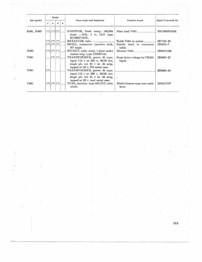
Model Ref. symbol N lurie of part and description Function of part Si~l Corps stock No.
1 234 -----------I----~---------I-----------I------
R401, R402
X401
T401
T401
V401
(*) (*) ('*) ---
(*) (*) (*) --(*) (*) (*) ---
(*) (*) (*) --
--- (*) (*) ---
(*) --- --- ---
(*) (*) (*) ---
RESISTOR, fixed: comp; 100,000 ohms ±10%; 1 w; JAN type RC30BFI04K.
RETAINER, tube _______ ,. _______ _ SHELL, connector: junction shell,
90° angle. SOCKET, tube: octal; 1 piece under
chassis mtg; type TSB8TI01. TRANSFORMER, power: fil type;
input 115 v or 230 v, 50/60 eye, single ph; sec 24 v at .25 amp, tapped at 22 v; HS metal case.
TRANSFORMER, power:fil type; input 115 v or 230 v, 50/60 eye, single ph; sec 24 v at.25 amp, tapped at 22 v; enol metal case.
TUBE, electron: type 6SL7GT; twin triode.
Plate load V40L ____________ 3RC30BF104K
Holds V401 in socket ________ 2Z7780-38 Shields bend in connector 2Z8276--7
cable. Mounts V40L ______________ 2Z8678.326
Steps down voltage for CR401 input.
2Z9607-27
2Z9608-58
Multivibrator-type tone oscil- 2J6SL7GT lator.
111
GLOSSARY
Section I. ABBREVIATIONS a-c _ _ _ _ _ _ _ _ alternating-current. a-L _ _ _ _ _ _ _ _ audio-frequency. bfo ________ beat-frequency oscillator. cps _ _ _ _ _ _ _ _ cycles per second. c-w ________ continuous-wave cyc _ _ _ _ _ _ _ _ cycles. db _________ decibels. dbm _______ decibels referred to 1 milliwatt in 600 ohms. d-c _ _ _ _ _ _ _ _ direct-current. DPDT _____ double-pole, double-throw. DX ________ duplex. f-m_ _ _ _ _ _ _ _ frequency-modulated. FS _________ frequency shift. h-L ________ high-frequency. h-v ________ . high-voltage. i-f _________ intermediate-frequency. K _________ kilo or 1,000. kc _________ kilocycle. l-f ________ low-frequency. ma_ _ _ _ _ _ _ _ milliampere. mc ________ megacycle. meg _______ megohm. mh ________ millihenry.
ms_ _ _ _ _ _ _ _ _ millisecond. mv ________ millivolt. mw ________ milliwatt. pL ________ plated. psL ______ -- pounds per square inch. r-L _ _ _ _ _ _ _ _ radio-frequency. rms ________ root mean square. RTT _______ radioteletype. SD _ _ _ _ _ _ _ _ Solvent, dry-cleaning. SLC _______ straight line capacity. SOP _______ standing operating procedure. SPSL _____ single-pole, single-throw. TD _ _ _ _ _ _ _ _ transmitter-distributor. term_ _ _ _ _ _ _ terminal. 'TT ________ teletypewriter. ua_ _ _ _ _ _ _ _ _ microampere. UF or uf _ _ _ microfared. UUF or uuL micromicrofared. uv _________ microvolt. v or V _ _ _ _ _ volt. VTVM _____ vacuum-tube voltmeter. w __________ watt. wpm _______ words per minute .•
Section II. DEFINITIONS For explanation of the terms used in this man
ual, refer to TM 11--455, TM 11--499, TM 11-680, and the following list: Ambient humidity.-The humidIty of the surround
. ing ttir; the room humidity. Ambient temperature.-The temperature of the air
surrounding the test set-up. Anodizing.-An electrical treatment given to
aluminum and other metals for the purpose of increasing the corrosion and oxidation resistance of the metal. The treatment is similar to elec-
. tro-plating but there is no deposition of other metal
Balanced mixer.-Also called a balanced modula. tor. An amplifier in which the tube control grids are connected for push-pull operation and
. the cathode circuit has parallel input. The plates are operated in push-pull, and the signal applied to the grids is balanced out and does not appear in the output.
Bia8 di8tortion.-This term is used in relation to the distortion of the square-wave teletype-
112
writer keying signal. If the positive and negative d-c pulses are not of equal length and of square shape, they are said to have bias distortion. See TM 11-680 .
Carrier 8hift keying.-An elementary form of frequency modulation in which a c-w (continuouswave) signal is shifted in frequency a small number of cycles. One frequency corresponds to key closed and the other frequency to key open.
Centigrade.-The temperature scale in which water boils at 1000 and freezes at 00 ; ordinarily abbreviated as C.
Current limiting re8i8tor.-A series resistor which will take almost the full voltage drop of the power source if the component with which it is in series drops to It low impedance .
Dot cycle8 per 8econd.-A measure of the equivalent frequency band covered by the keying of teletypewriter code signals.
Decoupling capacitor.-A bypass capacitor so placed in a circuit that the a-f or r-f currents of
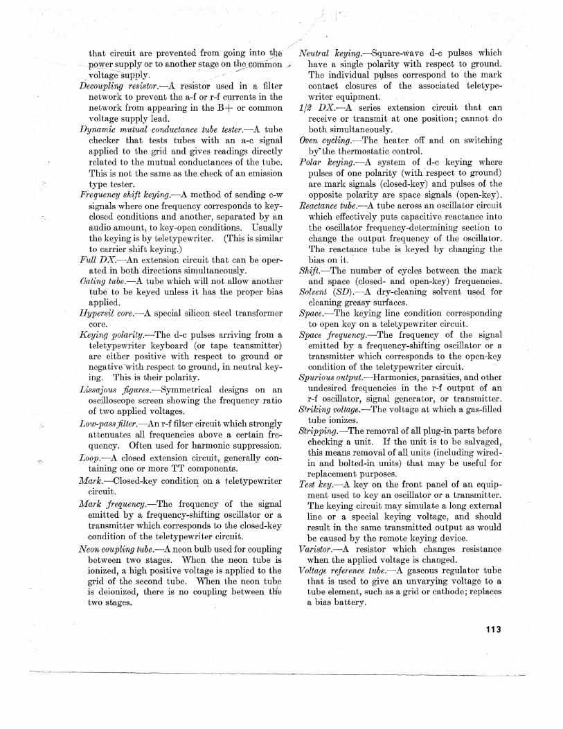
that circuit are prevented from going into the power supply or to another stage on th©ee:rnn;on ,
. voltage-supply. . -,-Decoupling resistor.-A resistor used in a filter
network to prevent thea-f or r-f currents in the network from appearing in the B+ or common voltage supply lead.
Dynamic mutual conductance tube tester.-A tube checker that tests tubes with an a-c signal applied to the grid and gives readings directly related to the mutual conductances of the tube. This is not the same as the check of an emission type tester.
Frequency shift keying.-A method of sending c-w signals where one frequency corresponds to keyclosed conditions and another, separated by an audio amount, to key-open conditions. Usually the keying is by teletypewriter. (This is similar to carrier shift keying.)
Full DX.-An extension circuit that can be operated in both directions simultaneously.
Gating tube.-A tube which will not allow another tube to be keyed unless it has the proper bias applied. .
Hypersil core.--A special silicon stcel transformer core.
Keying polarity.-The d-c pulses arriving from a teletypewriter keyboard (or tape transmitter) are either positive with respect to ground or negative'with respect to ground, in neutral keying. This is their polarity.
Lissajous figures.-Symmetrical designs on an oscilloscope screen showing the frequency ratio of two applied voltages.
Low-passfilter.-An r-f filter circuit which strongly attenuates all frequencies above a certain frequency. Often used for harmonic suppression.
Loop.-A closed extension circuit, generally containing one or more TT components.
Mark.-Closed-key condition. on a teletypewriter circuit.
Mark frequency.-The frequency of the signal emitted by a frequency"'shifting oscillator or a transmitter which corresponds to the closed-key condition of the teletypewriter circuit.
Neon coupling tube.-A neon bulb used for coupling between two stages. When the neon tube is ionized, a high positive voltage is applied to the grid of the second tube. When the neon tube is deionized, there is no coupling between tHe two stages.
Neutral keying.-Square-wave d-c pulses which have a single polarity with respect to ground . The individual PVlses correspond to the mark contact closures of the associated teletypewriter equipment.
1/2 DX.-A series extension circuit that can receive or transmit at one position; cannot do both simultaneously.
Oven cycling.-The heater off and on switching by'the thermostatic control.
Polar keying.-A system of d-c keying where pulses of one polarity (with' respect to ground) are mark signals (closed-key) and pulses of the opposite polarity are space signals (open-key).
Reactance tube.-A tube across an oscillator circuit which effectively puts capacitive reactance into the oscillator frequency-determining section to change the output frequency of the oscillator. The reactance tube is keyed by changing the bias on it ..
Shift.-The number of cycles between the mark and space (closed- and open-key) frequencies.
Solvent (SD) .-A dry-cleaning solvent used for cleaning greasy surfaces.
Space.-The keying line condition corresponding to open key on a teletypewriter circuit.
Space frequency.-The frequency of the signal emitted by a frequency-shifting oscillator or 3
transmitter which corresponds to the open-key condition of the teletypewriter circuit.
Spurious output.-Harmonics, parasitics, and other undesired frequencies in the r-f output of an r-f oscillator, signal generator, or transmitter.
Striking voltage.-The voltage at which a gas-filled tube ionizes.
Stripping.-The removal of all plug-in parts before checking a unit. If the unit is to be salvaged, this means removal of all units (including wiredin and bolted-in units) that may be useful for replacement purposes.
Test key.-A key on the front panel of an equipment used to key an oscillator or a transmitter. The keying circuit may simulate a long external line or a special keying voltage, and should result in the same transmitted output as would be caused by the remote keying device.
Varistor.-A resistor which changes resistance when the applied voltage is changed.
Voltage reference tube.-A gaseous regulator tube tha.t is used to give an unvarying voltage to a tube element, such as a grid or cathode; replaces a bias battery.
113
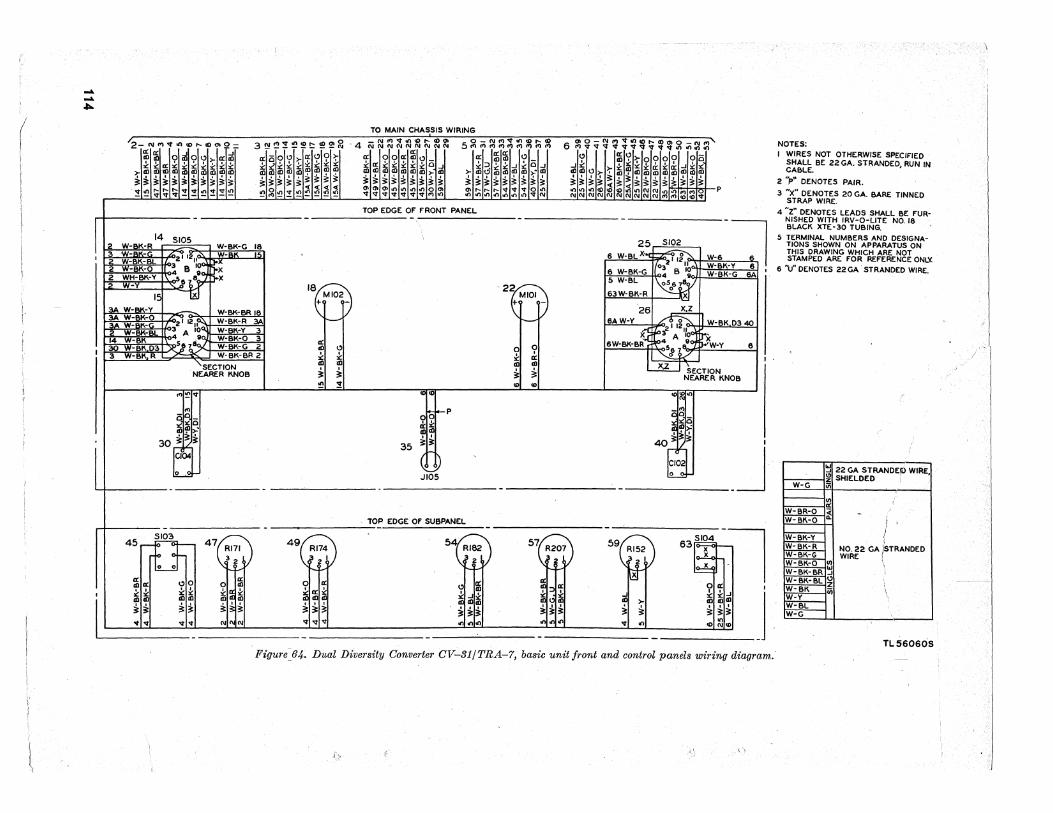
(
... ... "..
112 I :3
2 2
TO MAIN CHAS,SIS WIRING
'i~ -~-;;~ .n cD ,... cD '" 0 = 3 ~ ~::! !! ~ t:: ~ ~ 2 ·4 C\i ~ ~ ~ ({) ~ f\i ~ g: 5 ~ (;l ~ ~:r~r~ ~ ~ ~- 6--~~ ~~ Q : ~~ ~ ; ~ ~ ;;; ~ ~' ';l; ';l; 0 al 0 >- «Ial 15 0" «" 9 >; «00 « ::i " -1 «';l; ';l; "- '? ';l; <;> >- 0 0 00 0151 ~~~~~~ ~~~ ~~~ ~~~~ ~~~~~~~QJ ~~~~~~oJ ~~ ~~~~tt~~J~~
>-Ico cO 'cO en d) d) dl dl IX) cO d) en cp d) 'P cp m co cO co aJ co dl >- If) >- d1 t.:) dl dl dl dl 'r" cD en cO t) >- :: co 'P en cD co co dl dl co to
~~~~33~ ~33 3~~ ~~~~ ~~33~~~3~ 33~3~~33~ ~~~3~~~33333333 !~~~~!~ ~~~ ~~! ~~~~ ~~~~~~~g~ ~~~~~~~~~ ~~~re~re~~~~~~~~~ P
18
W-8K-B
TOP EDGE OF FRONT PANEL -J 6 W-6
W-BK-Y 6 W-BK-G 6A
-BK-O WH-BK-Y
-Y 22
W-BK-Y
18(~_ 3A W- K-O
W-BK 0340
tMIOln-
14 30 :3
'-BK- L -BK -BKD:3 -BK,R
SECTION NEARER KNOB
r')1~1~
C. I03 45r::tJ:
IIUI 47, RI71
3 2
a: ell ,,' ::0 ::0' ell 10
~ , ~
~ .,
--""""
910tP a:';: 1010 , ,
0 9
'" «
8
10 10
~ 3 '" '"
I
"~ _J ~~
lOP EDGE or SUBPANEL ----------------49, RI74
t-
54, RI8Z
~2
57, R207 59, RI52
';l;« ,,0 0 ~ 0 a:1
I '" '" '" ,l: '" II: '" '" « ,l:, 'P'!' '!''? ,!,!'P '!''?'P~ ~~ ~~ ~;>~ ~~~
~ q- ..,. "if ('IJ (\J C\I o;;t "'" ~
~ 'ex;
, 10 ~ J~
1010
33i 01) ",01)
~~I~'l' " ill! , , , ~~~ ..,111'11 "'I
~,X>;-~ ~ ., 00
---------Figure= 64. Dual Diversity Converter CV-31/TRA-7, basic unit front and control panels wiring diagram.
NOTES:
I WIRES NOT OTHERWISE SPECIFIED SHALL BE 22 GA. STRANDED, RUN IN CABLE.
2 "p" DENOTES PAIR.
3 "x" DENOTES 20 GA. BARE TINNED STRAP WIRE.
4 -Z" DENOTES LEADS SHALL BE FURNISHED WITH IRV-O-UTE NO. 18 BLACK XTE'30 TUBING.
5 TERMINAL NUMBERS AND DESIGNATIONS SHOWN ON APPARATUS ON THIS DRAWING WHICH ARE NOT STAMPED ARE FOR REFERENCE ONLY.
6 V' DENOTES 22 GA 'STRANDED WIRE.
~122 GA STRANDEfll WIRE" I I~ SHIELDED W-G on
b;-;--=c;::-o:-;~' :=~~=g ~! W-BK-Y w::i3K=R ~ W-BK-O III W-BK-BR ~I W-BK-BL ~' W-BK iii W-Y W-:CBL W-G
NO. 22 GA jSTRANDED WIRE )
TL56060S
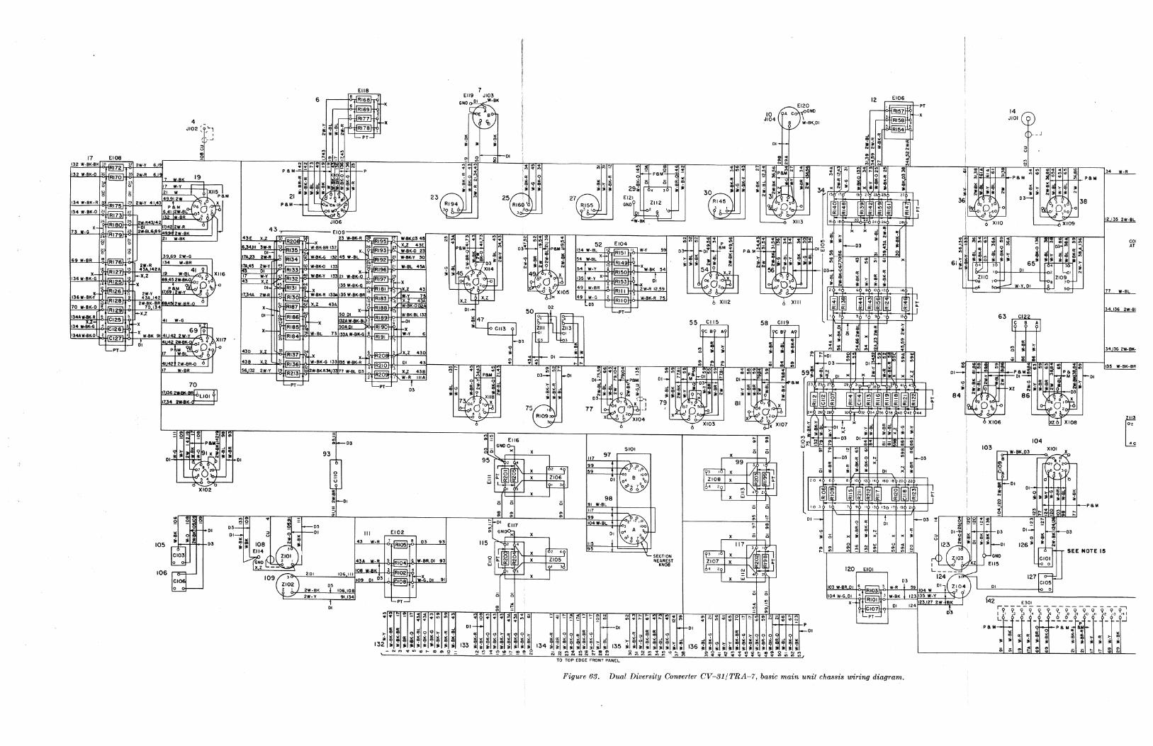
4 JI02 : -~\..,
17 EIOS 619
I ("_...J
132 W-BK-BK • ..JRi72L" 2W-Y
132 W-BK-O l6 ~RI70}~'~~'2"1I:--R"--'6"'1~~~::f~19~:;:=-1 l:r= ~ 7 W_RK
lf !l !~:9~: t~lI~plM 134 W-BK-RU!URI75 1 ,., 2W-Y 4143,1 /c 7. X
134 W-BK-O za~R173i ~ .:. 82~_Bo?t·,~, 2.~ 25 1 .... R4314 I I
X I~ I:!!' __ 1114212W-R 0 73 W-G R179 23 2W-8L .... 9 "f2W-B.
~'I!!!..U<J ~ 21 W-BK
~ ~ 3969 2W-G 69 W~ 181iii76L ~ 2 R 134 W-BR
13~" 4t'42A .n,41 X !-X Z 19 Wool XII6
136W-BK-G ~'. ~r?; x· 69:~:W~~~05\, <>
w_T ~:t 2W-Y 1169i2W-Y~·· 7 136W-BI<-Y --, 43A 142 J
IO~RI28l 2W.BK-BR~.et~R~ 6 70 W-BK-O • RI29 7 70 134
l34lw.llK·R : ~=CI25 ~ •. :X,z 41 W-G t 134 ... iitG CI26 69 I' 134AW-III<-0 , CI27 I X W-BK 91 41142 2w_Y
2_.,~' XII7 DI O' <>
'-PT- 17 pt=-B~ljo • 41 42' 2W-BR.0 <) 17 W_RR
70
17J362"'RK_~
= :1--03
93
EII8 7 EII9 JI03
'~r® " ID
;0
" "'''' ••• II: 1;1' "I~ N mil£' 'I~ 0:
I ~·I'. 23 .. RI94 , ,
Ci ;; .. .. .. ..
x
Ci
.. 51
r- DI D~ 5! • {-I--D3 DI-,. i3 ql-;t--DI III EI02
~rDI EII7
:glGN~
.. ..
i ~ 105 ...:.J:~t"'t-t-03
E3 106~
1~1"l-~
" .. ,. ID ~4",3,--'W",-",R,-+.cj7'11'RiO?,tr:.+-"D ... 3_~9"i3
; ~xll:z: J_~ 43A ",_R • ::u. W-BR.DI 93 I~~' L~ 108 W-BK I 1 ~ I~==== • ~ crt 201 106 III :. RI02 19 ......
109 ' l,ng 1>1 03, 108 rf'",:J;.ol 91 ZI02 1'---' , <>;' -r-...l2;,>Wo.;-",B",K_...l't ... 3-",IO",6""O",S"l 2
2W-Y 91 134 '-PT-
115
1
.-o .... 0 0 I '1l-'x:--1~'=',.. ~ 0.. ~ ~ /I-_X"--li-Z::;I;.:0..:;5.,
," I ~ x
~ ~
27~n; RI55
, I
117 97
91 W-BL
~ri-paJii ! ~ , .. ii Q 0 ~ ~
29;0 o. '0'. EI21 GNOY I ZII2
~~ Ie
.cW-BK .
SIOI
~~W-BL ! ~_-<' ,f"o ~ J A 100
01 04 8
II~ j ';>8 9~ +
SECTION NEAREST
KNOB
... .. ... '"
3~i~ RI45
~
99
10 A c GND r;J.EI2~0 ,J104 ( W-BK,DI
DI-r
m .. .. .. .. ..
DI
EI06
.. .. .. .. : ;; on ",r--03
N II! X Ii ~IO~ I : '~IJ~~ ,,:.:.;..:..:., +'-'--,.,-h. 0:: 0:: z o. _ ~.±_-:.±'::0I:!-:12±,::,~, • .:.0_'::~~zo±z::z~---1h
[~[~ [~~ ~ ~ OO~~ ~ 5 - _ z OJ
117
on .. .. .. Ci
.. '" Ci
Z107: '13 0::: ... ;=:"=-+-"---h ~ i2 Q.
4 2 ~ 4 2
x '" ;;
10 ,
01_
, . II 13 150 17 19 21
J, o 0:
0: :i: .. ID N
)C •• )(
120 ,,,,E,,,IO,,-I_-,
103 W-8R 01 • JRiOil ' I04W-G 01 ·I~,
x-I-II~ I~~,
'-PT-
0:
x )( •
01
Figure 63_ Dual Diversity Converter CV-31/TRA-7, basic main unit chassis wiring diagram_
63
14 JIOI
" u
CI22 C B
103 r::- W-RK D3
B
~ °A
<S I-
W-R
COl AT
W-BL
4136 2W-BI
3'!L36 2W-BI<-
b
'" ID ;0
P8M
SEE NOTE 15
E'3 0,
'0
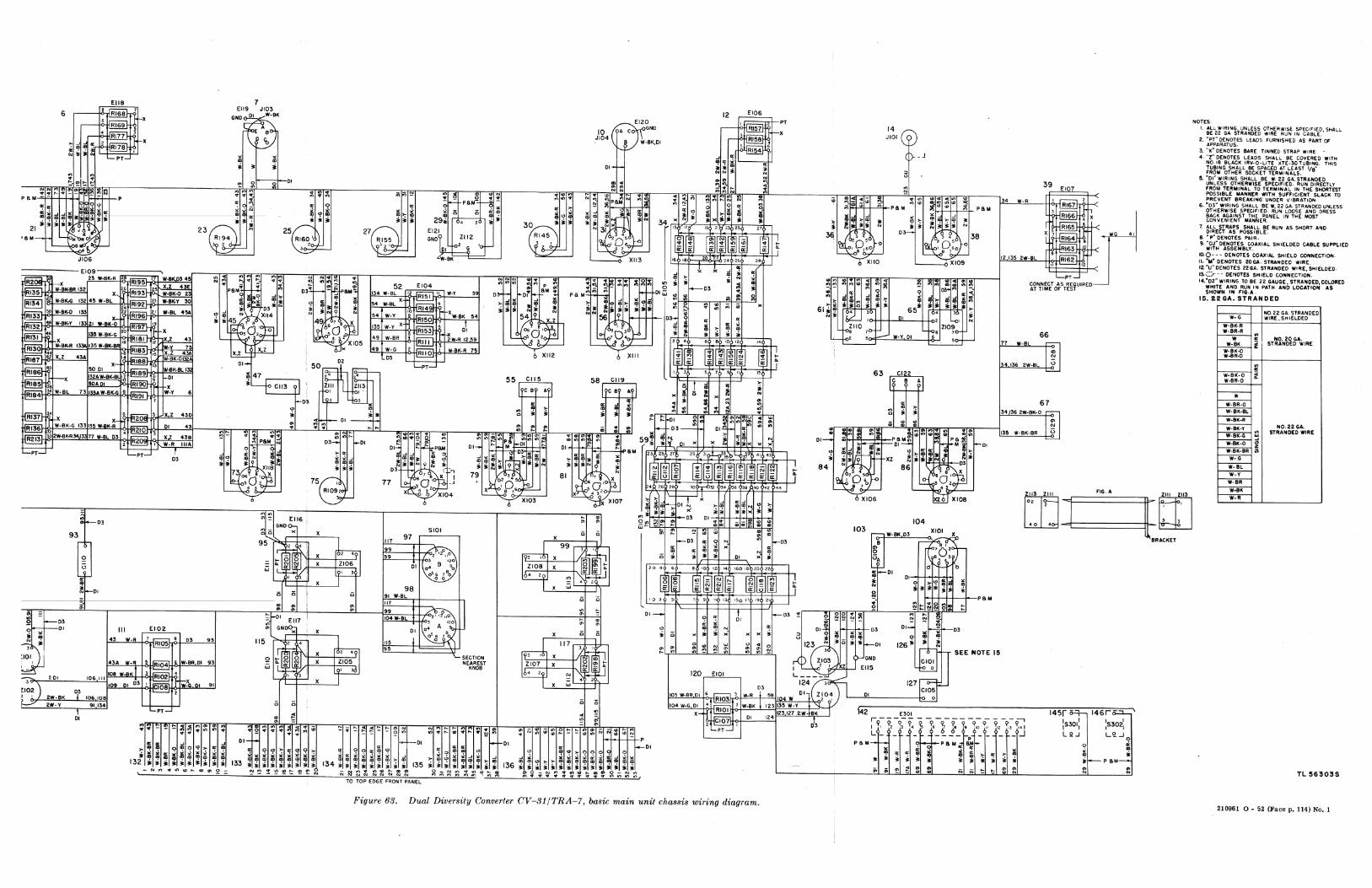
;;; = 8 -1--03
ql--;;;I--OI 31 III
~ 30
~:;10_311
JI06
~ ~1-03
93
..
x
23
III EI02
43 W-R 7 -1fii05'. 03 93
1=
43A W-~ RI04 W-BR,OI 93
91
01
_ GNOo-. ; _~ .. ~ E116. "
o xl X
95 1_' 41 X I- 0 0, ~'1064 0.. C\I N J X wO::O:: AI----"---+~==,
I" ~ '-(I=f::t-lLX --.J
:: 3: ! ~ 01 EII7 I
~ GNOo;] 1 )(
X
.. '"
, 4
SIOI
117 97
99 59
91 W-BL
117 ~ A 100 :'W-8L e"Ii'''O
01 04 8
115 j 0'8 95 j
SECTION NEAREST
KNOB
x
... .. .. .. Q 0
... .. .. .. X is 0
12
o 0:
~ ¥ o CD CD N :a 0 )( •• )(
~~ ~~~~
120 EIOI
103 W-BR 01 6
104 W-G 01 4
X
PT
EI06 r;::::::=:;;:;;+.....PT
x
Figure 63, Dual Diversity Converter CV-31/TRA-7, basic main unit chassis wiring diagram,
103
paM
14 JIOI
::> u
W-SK 03
01
34 W-R
"'f-+-++-"'1- P 8 M
38
12 1~5 2W- L
PT
~~NT~~CET o'}S&~~UIREO
104
d b
" ID
;0
01
66 77 W-
4136 2w-BL
67 34 36 2W-BK-O
135 W-BK-BR
1-I++1I--+-P 8 M
03
... ...
SEE NOTE 15
" i ~ • Cit N ~ t: := g:
WG 41
NOTES:
t. :~L.2;1:~N~t~:~5i5 ~~iR:~SNE I~P~~~LEE~' SHALL
2. "PT" DENOTES LEADS FURNISHED AS PART OF APPARATUS.
3, "X· DENOTES BARE TINNED STRAP WIRE .• 4. tor' DENOTES LEADS SHALL BE COVERED WITH
NO· 18 BLACK IRV-O-LITE XT£-3O TUSING. 1"HI$
iW8~N1,.mGiL~~KSlf1\OR:TNL.:ts~T Ita" S. '01" WIRING SHALL BE W. 22 GA. STRANDED
UNLESS OTHERWISE SPECIFIED. RUN DIRECTLY FROM TERMINAL TO TERMINAL IN THE SHORTEST POSSIBLE MAIIINER WITH SUFFICIENT SLACK TO PR[VENT BREAKING UI\IDE~ VIBRATION.
6. -03" WIRING SHALL BE W, 22 GA. STRANDED UNLESS OTHERWISE SPECIFIED. RUf>4 LOOSE AND D~ESS BACK AGAINST THE PANEL IN THE MOST tONVENI ENT MANNE".
7. ALL STRAPS SHALL BE RUN AS SHOAT AND DIRECT AS POSSIBLE.
S. .. p" DENOTES PAl R· 9. 'CU" DENOTES COAXIAL SHIELDED CABLE SUPPLIED
WITH ASSEMBLY. ~O- - - DENOTES COAXIAL SHIELD CONNECTION. II. -M- DENOTES 20GA. STRANDED WIRE. 12. 'V' DENOTES Z2GA. STRANDED WIRE, SHIELDED. tS-C.:r-- DENOTES SHIELD CONNECTION. 14."02" WIRING TO BE 22 GAUGE, STAA"DEO,COLOREO
WHITE AND RUN I N PATH AND LOCATION AS SHOWN IN FIG •••
IS, 22GA, STRANDED
W-G 00.22 GA. SlRANOED WIRE. SHIELDED
W-BK-R W-BR-R on
W 0: ST~~Nt~CAWIRE W-BK i W-BK-O W-8R-O
on 0:
W-BK-O i W-BA-O
W
W-BR-O W-BK-BL
W-BK-R
W-BK-Y NO.22 GA. on STRA"OEO WIRE
W-BK-G ... -'
W-8I<-O ~ z W-BK-BR ;;;
W-G
W-BL W-Y
W-BR
W-BK
W-R
TL 563035
210961 0 - 52 (Face p. 114) No.1
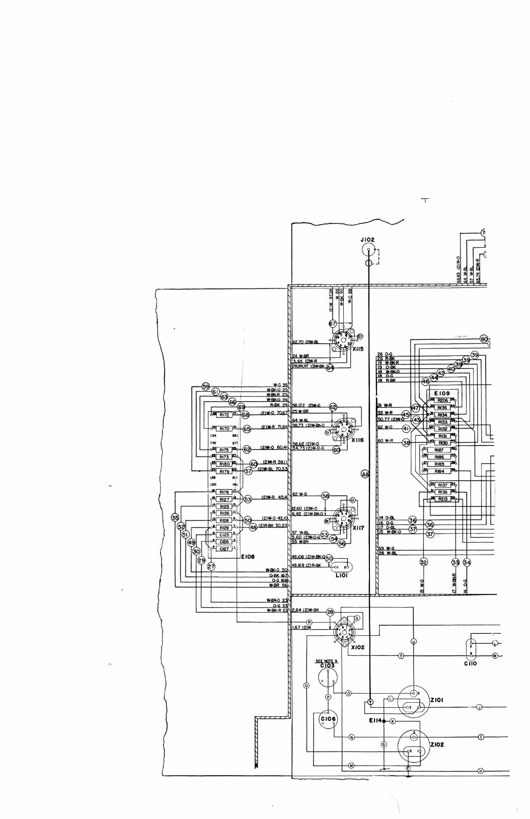
)
(
I
J
J
\
-JI02
~ W-G35 591~~~----+------~~~~~251
6J.;r.:~ I ~R.2! ~~~~·~'~,r.:~~r------~~~~~~·~AAI
::::: '::::~ ~ ;;: ~ti.~. a oM 330i ~ ~ ,.0. 032 5''1 ' 158_S2 !21W-O 0 X 116
~ ~"@J~-.w (21WII!:--:2.J06~0!.141f-1 ~4t17~3[2illlW~-Q:O-LG:_~(6;~~j
"l.R!ZU"f' ~ ---f'6I\. 12JW.R 38.11
~ ~21W-Bl 70.5~
.~ "" IM~" '?1Al---, ~fj@ 121W-R 45.4 r CI
.------t<~>914 RI25 ~ 260 !21W-O a
~~ ",.'0 ""0 I •• " ~>W-""'3 ,..---jooL ~!21R-8K 50.2~ ,~. 0 XII7
57 w-",- 53 I_se [2JW.. I-G'
49 CI26 r 155 W-BR
~. ~ 29 £108 ~9JOS t2lW~ l~ ',6, ~.169 !21R-BK fLo, z!) ~ W-BK-O 50 ~ ,--L..-t+_1-__ ~:r _______ -___ 1!-_-_-_______ -_...Il--,:n.""·;RK~~If\1N7NII LIOI
O-G 1613 W-8R 56
Q-G 2~
, I
(~J
£109
~WlR ~~ 53 W-R _c;;;., ~ i -"II ~--5O.nl?lW~ lfAi\ - RI34 r>" r-
~ rout RI33 S2 W-D. 41 V iU32
~ Al""L~ ro W-R '3"" ~ - ~ c['-[ RI87 l"""
159 w.G 126 wa
=t. Rlas -F? ~ RIBS !""" (]I'! R184
~~ I~U"'i""L R213P
L..-------: __ -_________ -_--"W-:_BK~-:!.!R:2_"'t~tlt_2-6-4_( t:21,:-BK '~r'H~-o--S--.
I 67 (2)ii,f • r. 8 I I t-!r""-'-'.....".----....L..pI'H~ 0 ~
r---~~5~W~~-1~ u
r-f-
r-
•
:
"~;102 I IL-'--~------_(T~~------------~.~--~Iw ~
SEE NOTE 9 en 'tl~
Q
CliO
r®- f~ZIOI ~D \ ( 2 ~.p'-H-\ }--------G>------1 ,,~_
CI06 o EII41~~-"'"
f--®}----+------r-~--+<>-l+""~------{I }---( ~~:ZI02
~f___----_+----------~~~~(·2 ,
~~
G
L------r~~r_------f__~----~(t-~
lL-_________________________ ~~~~====~~~~~~===~====~~=============~~~H~=====
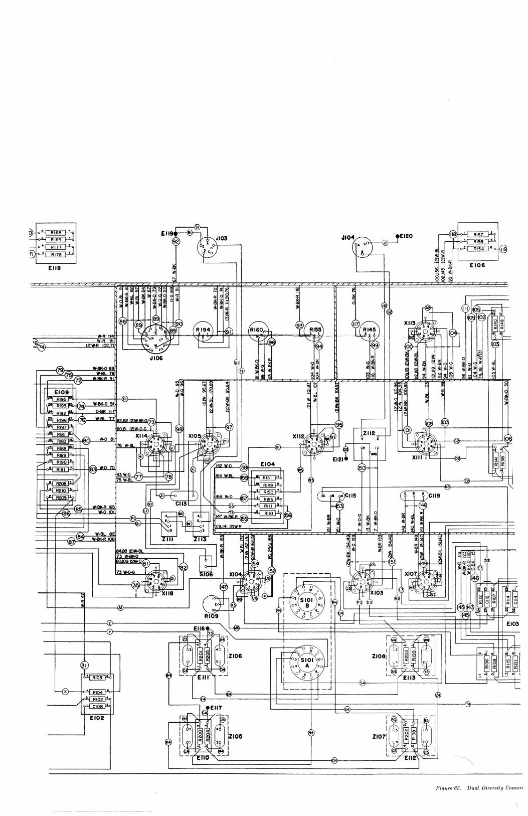
74r_--------~~-W~·
L-~----~~------~~r_--------------~
---4------~----~zr_--------------------------~ ---r------4-----~yr_--------------------~
-1 / I IZI06 I I
_:..1
I Z108/
I I
T------r1-~~----~s4~r_------+_--------~L------~=r~===i= L___ _...1
~~~----~----------~--------~~ L---------t------+--~--------------------------~----~~I~--------------
U4
r I /
Z107: I I c L_
04r----------------/
Figure 66. Dual Diversity Converl
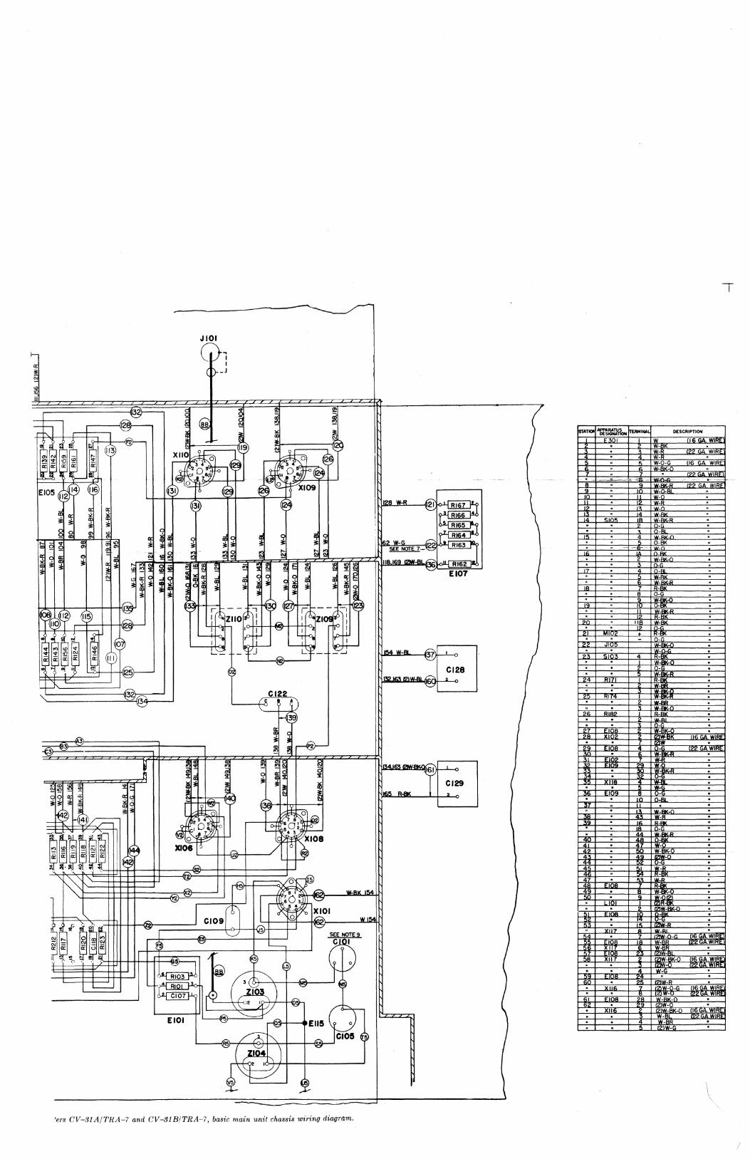
'---------tl3·?.....,~--' ~----------~~14'--~
3 3
EIOI
JIOI
'ers CV-31A/TRA-7 and CV-31BITRA-7, basic main unit chassis wiring diagram.
DESIGNATION ~INAL F3C
,
" " "
· " .' · · 14 <:10'"
· . 1'\ •
, " I" . " ,
· 17 •
· " . IA •
" " .
,
· ~r ' , ~I M)J>
" 22 JIO: · ~.. <;11)3 , . , . · .
24 RI'
· RIA!
~7 FOR ?A le · .
E'IO~ FIOq · · · 36 E'I09 · .
3' " , .
· · 52
· · · · · · · · FIOA
· · 53 •
· "
1:1
· · F;
· · -,
lei
· 17
E08 XII7
· · ~
lell" · FIOA
XI6 · ·
~>"K'PTION
"GA. WIRE , GA. WIRE
l·G 116 GA. WIRE
· --, GA. WIRE .----.... :<> ;A IIIIRF
.AI
\AI_''''
(-R
lK_r
K-R
II-BK
1(..(
II?I
~W-RI<"(
~Ak 1'lJN· 1AI_r.
~-( ,-/,:
IK..(
, , " " ,
· · · · · ,
· · · · · ,
· ,
· ,
· · , ,
· · · · ·
) GA, WIRE
:bA.WIj'(!; · ,
· · · , · · · ,
" ,
" · · · · · " " · , ,
-"-
-', iGA.WIHE
--. ; GA.WIRE
(22GA~lHE ,
· , fl6GA.WIRE
"WIRE · · !l6GA.WIRE ~GA.wlRE · ·
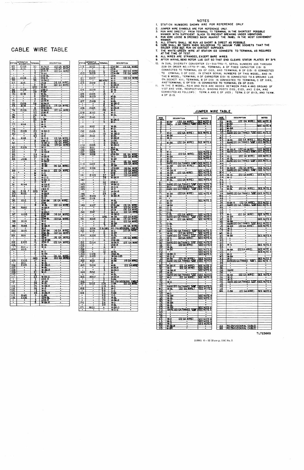
CABLE WIRE TABLE
~TAT DESIGNATION n ... INA, I I~""'" I"'''''-~T\J~,
6:'> F j)-R '-R 122Gb. WiRE 19 1';4 l'i BK 16 GA, WIRE , .-" " I?~ ;A WIRF I' ()h
-';- -;, , h'i FIOR " I? 17
-66 , "
-~7 "ii" 123 ~109 3 {2l" GAWIRE " ,
G · " 5
"" I' II> " "'" " .n<l "' " I-( " 1~6 09 3
0 0 · 4 --. ~-R 0 127 ZI09 I'IOq
II 7-'1 lC 14 (16 0 · 7.i: -J:ii\Q {2:' GAWIRF
-;
· " · I?A 1'10"' " " ,?< " "(
7'" W.RI · " " 7i': -.- ,,>:( lIe -. --. i:"Ri( 0 " 7 · W_R · , " 5
IA/, · · " IN_AI · 1'1 XIIC -jA --. ' , · " 7q no'! W-RK_I 0 rw .O'i -'BC , -woe " " hT- · W_R
IIA W I.r. 16 r.AWIRF 13'1
" · · ' rnw. i9? :4 WIRI' .. W
" · 1?IW-Rl O<:i!GA, WIRE 1>'1 ' .-'0& 'IN, · "" .. , W_RI ,
-". .. ,. 'Ii/:Rii..R 86 -~ :>q -woe · A , 'II W-RK-R " -S8 = F W-):Bl -"
· , G W-RK.R · · · " W_RI · ~I?? '. -. -W.RK -116
· · IN -ACi · K W_RK (22 GA,WIRE
14( XIOs "
I' · · · I Q{ · " · I'll' · ,; • " · Qo A'" [4: .... '
• --; !R-C 144 · · · » · Q? EI19 t.1 -q-" '1'1''''''' -;;-
· " · 145 · " · 146 · 14R 1<1
'I" X I? -AK 116 GA WIRE · · ,- -.- " · 122 GA,WIRE 149 Xlf Q~ RI~r :.R , --. · · 9, XI05 '-61( tlG GA, WIREl · , · , · GI · , 1-81. {22GA, WIRE 151 XI03 9B XII4 · .
It: · 99 R14~ · · · inn vI,": tl6GA, ,llTlE'
· · · · ,<;, ",n4 i? Po,.... , .... II" · " .RI I?? r.11 WIRF' , , -.:n; -"-'1 · 154 XI04 , ,
" · !f-RK JmI- '1'11'11\- :R (22r.lI.w,R!'" EI04 lin , · · liff
To4, " '" .-• • '-iii: · '''''' 116 GA WIRI' - '9 .. 122 GA-WIR£ · · 10'> F ,,,' XIOI , l/ · --1"11'1" · ,~ .. <;'04 -. · · _R · " · · . '1';4
--;- , , · , ':1\- 0 165 Rl'r · 0 Il'l I-R · · " • -w, ~R · --. W· · ,Ii( \AI, ~". , · · ,~ W- · I"R -. 1'1 w_
IN: 169 R14'i
:It ,
I'ln~ · · · .' · · · " · ,
1'70 · · " 17 M · -
DESCRIPTION
21W-BK If, ,A WIRE! ')W " ?IW.R (22 GA, WIRE
21W 122 ;AWIRE
I-C , IN, " I'.'
.... _AI W-C · 1'.'-1 · 1'.'- IK-C · 1'.'-' · W· _R · 1'.', IN · W-B · · W-BK-O · W-{ ·
-Bt · · -R! · 'IK-D · · K-R 0
· · · · I-Bt · I-BK !l6 GA,WIRE
122 GA,WIRE W-IR .. I?l (16 GA WlRf
122GA.WIR!
1.$11( 1I~r..,.'I 122GA 16 r.A
IK-R · . · 21W-C · '-BK N-O-G · N-R "
-RK_R " _AK "
" · · · f-RK (16 GA,WIRE 122GA,WlRE rl6 GA,WIREl
IK l~. -BI<
!R 116 GA,WIRE~
lOr, ?QJI iCOAXIAL ::AlII Fi W. 1000i!GA,WIHt. W-BR · 11 · 116 GAWIREI · 122 GAWIRE · WoO "
" -BL .. 0121 · ·
IA/. 122GA.WlRE w· [.R ..
:..n ..
" :-R ~K ·
· · · · · :_R
· · K-C 0
'-G ·
NOTES I. STATION NUMBERS SHOWN ARE FOR REFERENCE OHI.Y
2. JUMPER WIRE SYMBOLS ARE FOR REFERENCE ONLY. 3. RUN WIRE DIRECTLY FROM TERMINAL TO TERMINAL IN THE SHORTEST POS!iIBLE
MANNER WITH SUFFICIENT SLACK TO PREVENT BREAKING UNDER VIBRATIONS. 4. RUN WIRE LOOSE a DRESSED BACK AGAINST THE PANEL IN THE MOST CONVENIENT
MANNER. 5. ALL STRAPS SHALL BE RUN AS SHORT a DIRECT AS POSSIBLE. 6. CARE SHALL BE TAKEN WHEN SOLDERING TO VACUUM TUBE SOCKETS THAT THE
SOLDER DOES!!QI RUN ON CONTACT SURFACES. 7. THE WHITE-GREEN WIRE AT STATION 122 CONNECTS TO TERMINAL AS REQUIRED
AT THE TIME OF TEST. B. ALL WIRES ARE STRANDED, EXCEPT BARE WIRES. 9. AFTER WIRING, BEND ROTOR LUG OUT SO THAT END CLEARS STATOR PLATES BY 3/'S.
10. IN DUAL DIVERSITY CONVERTER CV-3IA/TRA-7, SERIAL NUMBERS 203 THROUGH 209 ON ORDER NO. 11779-P -48, TERMINAL A OF FIXED CAPACITOR CI31 IS CONNECTED TO TERMINAL 29 OF EI03, AND TERMINAL B OF CI31 IS CONNECTED TO ERMINAl C OF C122. IN OTHER SERIAL NUMBERS OF THIS MODEL, AND IN THE B MODEL, TERMINAL A OF CAPACITOR CI31 IS CONNECTED TO A GROUND LUG O~.SOCKET XIII, TERMiNAL B OF C131 ISGONNECTED TO TERMINAL C OfCI22, AND"TERMINIILC OF"CT~I IS CONNECTED TO TERMINAL 2'9 OF E103. .
II. IN THE B MODEL, R214 AND R215 ARE ADDED BETWEEN PINS 4 AND GROUND OF VI07 AND VIOa, RESPECTIVELY. BINDING POSTS E122, EI23, AND EI24, ARE CONNECTED AS FOLLOWS: TERM. A AND EOI' J103; TERM.2 OF i!1I3; AND TERM. 4 OF i!1I3 .
Is::'
t-
'V
X V
R
E F
'" HI
)(
Mi
I
VI W x
JUMPER WIRE TABLE
DESCRIPTION
- iA !RAR· Q GA.TINNE
0 · · 0 · · IW..( 1~~uA,WIRE
I WcBK 0
i W- 0
, IW-BK 22 GA. WIRE · · · ,
· · -22GA WIRE
- , - , - · A (2 ) GA. INN "'l'lI/il' - 1i!0<: uA,WIRE - · -3K,R · -- · IIN_"'''_'' "
IW-Bl (22 IRE
· RARE- (20 GA, INN '..II -
TI -WI!!!ll'" ,
!W-RK 122 Gil, liRE !w·r. ,
, · - ~K · - , c'IK · , - · · -
I"'''' ~FI20GATI lw" 'IK .1Z2.GA · · - · · - · 12C'GA '!.l,lIO·
- 122 IE: (2(1 GA,
- , R 20 GATINN oD '~l1.'r
W_ 122 GA,WIRI" - · W-B · · · IW-BK- · W- · -
I BARE {2( .GA. INN '~lII'.r · . -RK-R 12:;> 1NiRi'"
11'.'- {~2 .WIRE W_AK_R · · BARF
IW-C 122 GA,'WIRF . - " · · 1GA. >,Il'IF
·W-B! 122 ,.WIR~ 0 ,
· I W_ ~R W-1'.'- , W- BR · W-Bt · w"BK ,
ARE!20GA. I -...nw · · · · · · W- 122GA RF'
IW-G " WoO · IW-BK-R · ·
NOTES
I"iI"F'NOT£4 'NOTE 5
· · · I5EENOH , ,
EE N( rE4 , , "
ISEE N< TE I~F Nr"rr4 !SEE NOTE
" i<WF'l\IOTE 5 1<:~~Nif" , I""",, Nr"rr 4
EE NOTE4 ,
~"N TF " ,"-FF tJ( rF 4
· · I<;FF tJ( fF
· · " " ,
~E NOrl' 5
· · ,
[C;FFN( r. SEE: NmE4 I"-FE NOTF
'lIfiYfl'"'
· I"-EE NC rE I«J:-" Nt rIO . , ISEE: N TE IC;FFNnTF r~w'-,", · ISE:E: NOTE · ~~ i<;FFNnrF 1"-l'l"'f\IllTF" 4
· ~"N( I> [c;FF N(:rE
· I"-EF NOTE · · r~-NI' fr: I"-EE NOTE ,
· · 1~l"NOTF'-4,
J!WFlIIl T1""15 , · · """NOT" ~m-'"
I"-".NOTF
· ·
WIRE SYIIIIOt.
3 u
W-
- R 5 W-R
1'.'-
210961 0 - 52 (Face p. 114) No.2
DESCRIPTION NOTES
A. INN D w £:4ilIio.&..",N!o/.!..I'->I.j
20 GA TINNED E
.1'.'1
GATIN
A,WIR T , I
TI N
A IN EEN
2 GA.W1RE
TI
AXIAL
TL12366S
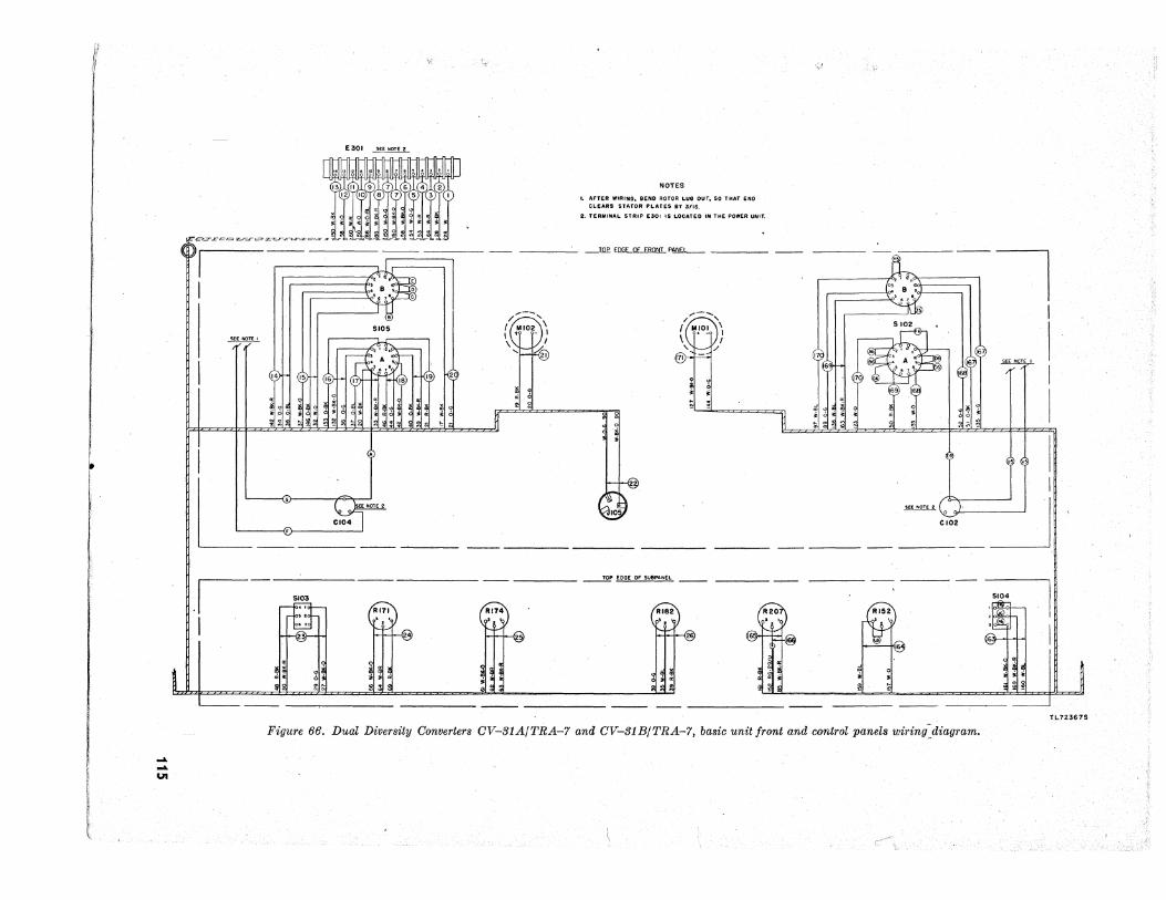
.... .... UI
\( \~.
E301 ~
~
I
lll= ' Qj
.1 $103
I
SI
NOTES
I. AFTER WIRtN8. BEND ROTOR LUG OUT. SO THAT END CLEARS STATOR PLATES BY 3/16.
2. TERMINAL STRIP £301 IS LOCATED IN THE POWER UNIT.
~ EDGE Of fRONT PANEL...- ____ _
-----.!2!' EDGE OF SUBPANEL
--- -- -------
y: p
-~ ~ III ..
$102
I =-1 ·1 CI02 ~
r~723~7S
Figure 66. Dual Diversity Converter8 CV-31A/TRA-7 and CV-31B/TRA-7, basic unit/ront and control panel8 wiring=diagram .
c-
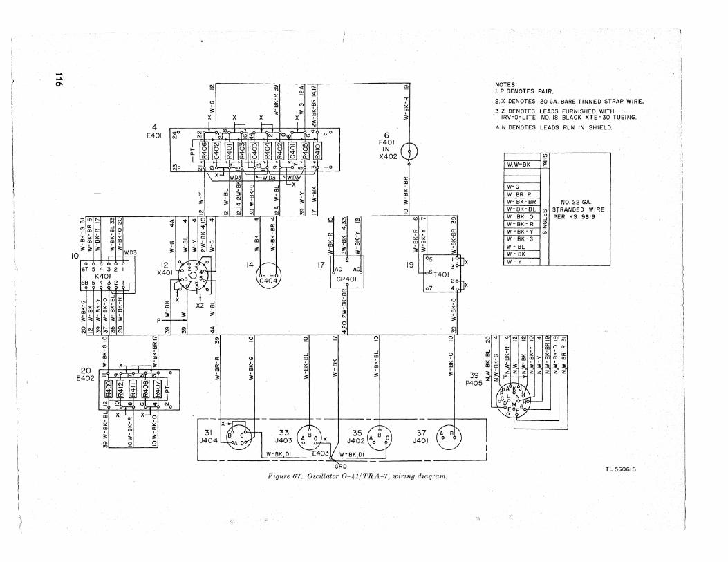
fT1 -1>
N
00
t\
)
20
W
-BK
-G
12
W-B
K
39
W
-B
K-Y
3
9 W
-BK
-BL
W
-BK
-G 1
03
7
W-B
K-O
""J ... "" '" ... '" '" :-<
10
W-B
K-R
I ~(;
I
0-
." IN
~
::
IIC
D '" ~
' -1>
0J
00
J
(>J
W-B
K-B
R 1
7
W-B
R-R
3
9
W-B
K-G
10
;?
W-B
K-B
L
10
" ;:., ~
C
""il
G)
W -
jjt\
a::O
I
0
'" -':::'. ~ ~ I W
-tH
\":'
1
."'<
35
W
-B
K-B
L
20
W
-B
K-R
I "
39
I W
-BK
391w
x
4A
20
l -~ I
x_
Q N
W-G
..
.
o 4
:E
-.,J
~ ". ;;.
10
W-B
K -
BR
"" "'"' S· "" "' '" ?
..... , CJ
1 '" ° '" (/)
'- -1> 0
J W
-BK
-Y
I 0
-.,J
0
0 '-
-.J
m
c..n
<.0
6 W
-BK
-R
17
-I
l W
-BK
-O
10 3
9
W-B
K-O
~
~
x x
-1>
0J
0<
.0
U1
-N
W-B
K-B
L
20
4
~I~I~I
~I~ ::
:: :
::: ~
~ ,
, ,
, -<
CD
Wa
JlD
CD
CD
OJ
OJ
C
DG
) A
'rA
A "''
'' "''
'' ::0
,
, '
, ,
G)-
< ::
00
OJ
CD
::0
,::0
N
.W-Y
4
N.W
-B.K
-BR
19
SIN
GL
ES
N.W
-BK
-O
19
N.W
-BR
-R
31
,,(f)
"' .....
::
0::
0",
1>
0
'" ",.
(f)O
N
, m
N
"'0
G)
Q)
1>
-::
. "'
- ::0 m
1 23
0 I o
x "
fT1 ~.j>
.
2't
2 o
~Z~Ol
t\)
f\ ~
;I> '"
-::
° m ::
'" I
0 CD
.....
'"
'" (/) PA
IRS
, m
1> ° (f) ::0
c '" Z
(f)
:I
m , P
9H
W-B
K-R
19
~
N
,-z
;ON
X
,,0
.....
<
0
0 O
m
'm
m
m(/
) °2
'"
Z··
'0
0
0 c::
..... .....
.....
..
... '"
m
'" m
(f)
(f)
(/)
"" N
jg
0
'"
0 .1
>
'" ::0
_
0
1>
Q)(
f)
OJ'
" '" 1>
rc
::0
1>
::0
()'
" m
"'-(f)
.....
XI
2 .....
'" '"
",0
m
':
: 0
OJ_
(f
) 0
.....
.....
..... I
::0
C
1>
2:>
" '"
~
~
::0
!"
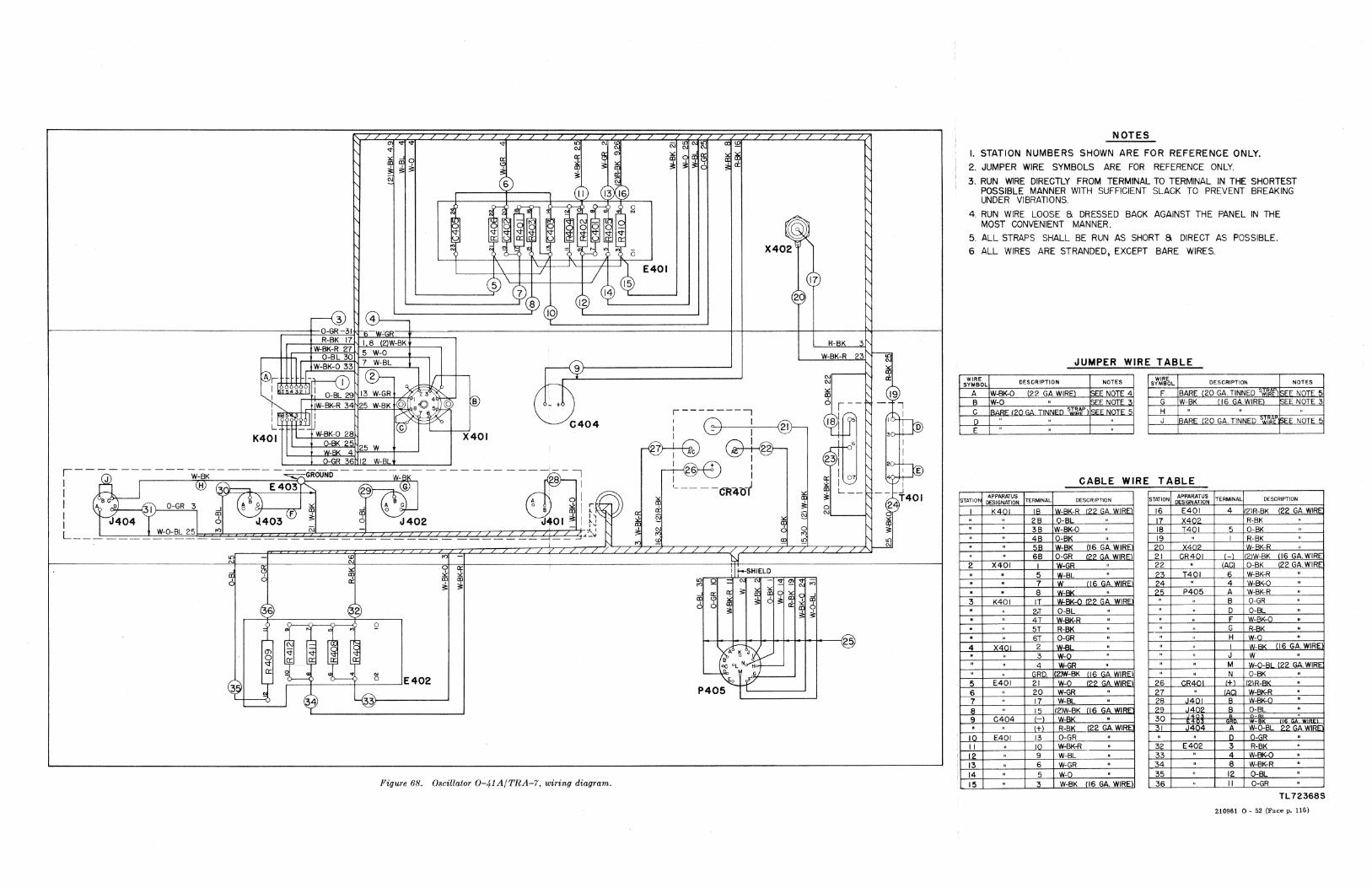
~ (6)
~\ / J~ E401
L--_----=:r~ 01 ~ rI4l ~"------I 8 ~ 12 Y L..-________ -..:I 10 '---_______ ---'
4;---....,
R-BK 17 I 8 121W-BK W-BK-R 27 5 W-O
O-BL 30
X402
~r I ~
W-BK-O 33 7 W-BL
ffir-0 ®- q ~ / ~r-----------~
I
l~ K401
I I O-BL 29 13 W-GR /?"/li 3~ b liw-BK-R 34 25 W-BK 0 ~O 4 0 f.!V I ~7'i
- - 'W-BK-O 28 '©' =t'L-u-4----.J X401
O-BK 25 25 W W-BK 4
-GR '16 12 W-BL
- +
C404
'---J- --- --- -W.:EiK------ -~GROUND----~.:;I<-- ------ ------1
: ~ Ct!) C', E403~ ~ I --r ' I B I O-GR 3 -J ~ I >£ ~ ~ U~. i I r 7
: J404 Y J 6 .{403 (f) ~ 6 0 J402 ~.Ol ~ I ~j L_ _ ~ W-O-BL 25 .., (\J =t""~~
. "" ... '" ~~~_v---~-+ __ o_~E402
Figure 68. Oscillator O-J,lA/TRA-7. wiring diagram.
I ...... SHIELD
17
2
,
I I I
I
NOTES
I. STATION NUMBERS SHOWN ARE FOR REFERENCE ONLY.
2. JUMPER WIRE SYMBOLS ARE FOR REFERENCE ONLY,
3. RUN WIRE DIRECTLY FROM TERMINAL TO TERMINAL IN THE SHORTEST POSSIBLE MANNER WITH SUFFICIENT SLACK TO PREVENT BREAKING UNDER VIBRATIONS.
4. RUN WIRE LOOSE 8 DRESSED BACK AGAINST THE PANEL IN THE MOST CONVENIENT MANNER.
5. ALL STRAPS SHALL BE RUN AS SHORT S DIRECT AS POSSIBLE.
6. ALL WIRES ARE STRANDED, EXCEPT BARE WIRES.
JUMPER WIRE TABLE
WIRE DESCRIPTION NOTES WIRE DESCRIPTION NOTES SYMBOL SYMBOL
A W-BK-O 122 GA. WIRE! IC;E:E NOTE 4 F BARE 120 GA. TINNED "WiRE SEE NOTE 5 B W-O " isEE NOTE 3 G W-BK 16 GA. WIRE ISEE NOTE 3 C RARF 11'0 GA TINNEn ~!!l.~ 1<:1="1" NOTE 5 H " ,
" 0 " "
, J BARE (20 GA. TINNED ',krt.r !SEE NOTE 5 E " " "
CABLE WIRE TABLE
STATlO~ APPAR~US
TERMINAL DESCRIPTION ST~ION APPARATUS TERMINAL DESCRIPTION
DESIG_ION DESIGNATION
I K401 IR IW~I?? r.J . WIREl 16 E401 4 121R-BK 122 GA. WIRE
" " ?R O-RI " 17 X402 R-BK " "
, 3B W-BK-O " 18 T401 5 O-AI< "
" , 4R O-BK " 19 " I R-BK " · " 5R IW_RK 16 r..A WIRE 2C X402 W-RK-R "
" " 6B O-GR I?? GA. WIRE 21 CR4QI I-I 2IW-BK CI6 GA. WIRE 2 X401 I W-GR " 22 " CACI IO-BK 122 GA. WIRE
· · 5 I W_R1 " 23 T401 6 W-BK-R " · · 7 W ~ 24 " 4 W-BK-O " " · 8 w::Ri( " 25 P405 A W-BK-R " 3 K401 IT I W-BK-O 122 GA. WIRE " " B O-GR " · " 2-T O-BL " " " D O-BL " · " 4T IW-RK.R " " " F W-~o " · " 5T R-BK " " " G R-RK " · " 6T O-GR " " " H w-o " 4 X4('1-1 2 I W-RI · ,
" 1 W-AI< Cl6 GA. WIRE
" " 3 W-o " " " J W " · " 4 W-GR , , " M W-O-RI 122 GA. WIRE
" " GRD. 12lW-BK~ " " N O-BK " 5 E401 21 w-o 122 GA. WIREI 26 CR401 1+1 121R-RI< " 6 " 20 W-GR " 27 " lAC) W-~R · 7 " 17 W-BL · 28 140 R W-BK- .. 8 " I') C2lW-BK 116 GA. WIRE 29 J402 B O-BL " 9 C404 1-=1 -W.:RK · 30 - · -" " 1+1 R-BK 122 GA. WIRE 31 J4 4 A W-O-BL 22 GA. WIRE' j() E401 13 O-GR " " " n O-GR " II " J() W-BK-R · 32 E402 3 R-BK " j? " 9 W-BL · 33 " 4 W-8K-O · 13 " 6 W-GR " 34 " 8 W-BK-R , 14 " 5 W-O · 35 " 12 O-BL , 15 " 3 W-BK (16 GA. WIRE) 36 " 1/ O-GR ·
TL72368S
210961 0 - 52 (Face p. 116)
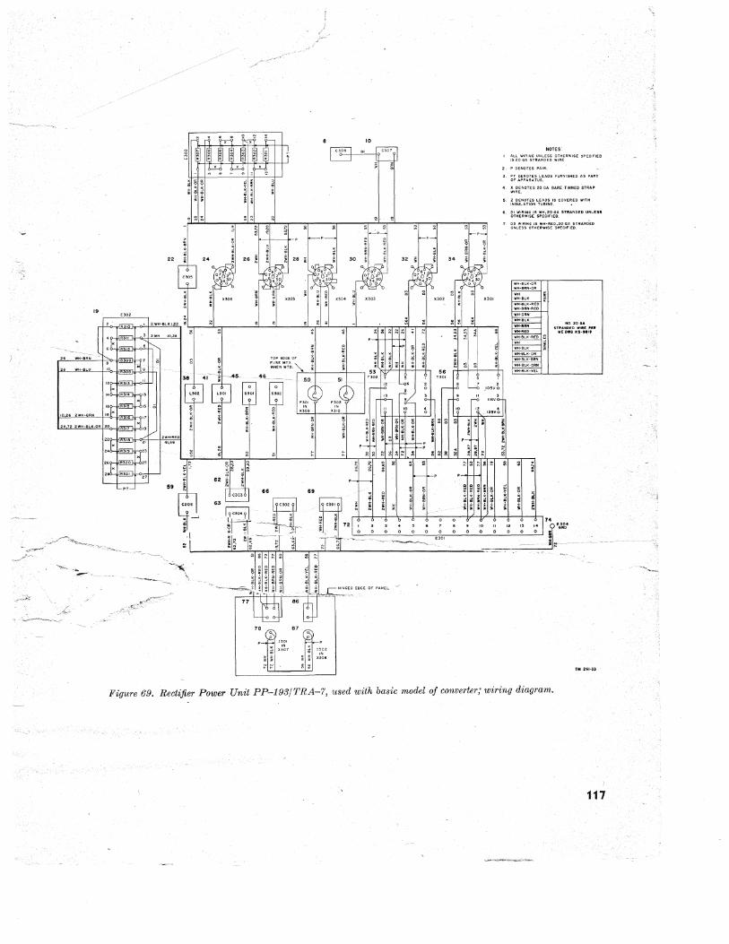
••
.. 2: I 2 WH·SLlC 1,22 l :5 i!:WH
--:--. )- "" '~Ij 2& \WI-BRN 09 ~,' _. • r="... 0
10 1'1308 9 -
10.28
12 11313 II I ,1~'J" 16~~;&15 Q
10,26 2WH-GRN 18 1 ..
24 12 ZWH-1Il II-OR 20 ~ :r:7
;t.!!.!I..L-:-019:.,.....-
41,66
5'
; ! · . • ± · .
••
a :
± ~ 28
~
1--,-
30
; ~ ~ ~ ~ ~ • ; ; ~ ,-~ ~ ~ ~
~ = ~
HINGED EDGE- OF PANEl..
~7~7~~~~~~~~~
• ~ i " . "'" ~ ~ ~ ~
3.
••
"
~ 3 ~ ~ ~ ~ ~
'" i; i ~ ~ ~-:
~ = ~ •
NOTES: I ALL WIRING UNLESS OTHERWISE SPECIFIED
1520 GA STRANDED WIRE.
2. P DENOTES PAIR.
, W .lOSV~
r Irsv~
" . _ J2SVQ
3. PT DENOTES L.fftOS "URNrSH!O AS PART OF APPARATUS.
4. X DENOTES 20GA BARE TINNED STRAP WIRE.
5. Z DENOTES LEADS IS COVERED WITH INSULATION TU8ING.
6. 01 WIRING IS WH.20 GA STRANDED UNL.ESS OTHERWISE SPECIFIED.
7 03 WIRING IS WH-REO.20 GA STRAND!O UNLESS OTHERWISE SPECIFIED.
WIi-alK-OR
~Kl ~: WH-BRN-RED
~-I ~ ~~ I~~
",0.20,. STRAN.DEOWIIiENIt WEI)W8I1S-'~I'
~ ~....L _____ ...J
Figure 69. Rectifier Power Unit PP-193/TRA-7, used with basic model of converter; wiring diagram.
117
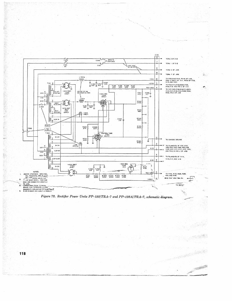
118
E301 ...--TERM 2 OF Zl12
F~~2 S302~>S~~~;S ~--~--------------~~~--------------~-r
F301 5301
\ '" \ 105-125~t;..... ~ 50-60 CPS \. ............
TERM. I OF Z 112
S303
,3A
1~126'3VIA ~ ~~
-ISU~~L'(1.. ....... _
T302 !-............
.' \ 10
L302* -ISOY .13
'/ V,VV I +C303I,bC30~41'R3~'l.7 ~=::o--=c=---;:-=---:=,-____ '::'c::75:::V+3>-t_ aUF eUF R31e R319 R320 R321
~ ~ ~_-~·_-+_lv'0~0_~IZvO~0~1'~0~O~vl'~00-r_~_~R:::EG~·r'5~OV~04-r. 12HISO OCMA L R311 C30& I 19S0I"NS DC RES "'.SOY REG 47.K 2UF~I*
\ Y304 6V6GT ~-, ~
L30,* ~rf? I R312 •
'000 J.' I 3 In 7 j-l-f---r---,.-' 4700 L-- :,
~~~'IC6t~21 4 5 2 r--- I
I .nrn 1302 r'H (RED)
R309 Z7K
C307 ,IUF
R313 I 660 I
R314 1500
R31S "00
f---<'
1~9 5V2A ~ 11 ')4 65J7Y
4 I~ 5V.. ~~~riO ~. Z 7 I ~ 1 2
12sY~~llllP::...J7~_-+ ___ ~=.::rb::J.t+_":"' __ J+ ______________ t-...J 6.3V I
R310 Z2K
R 316 4700
L_~3o.'.O <;lIil\Q52 6.'V OA I 115V ; ~ IPe..~5 __ + ______ J. _____ -L ______________ t-__ 105V ~ 10
I lis<: 6.3V2.~ II""
13
TERtJ. G OF Jloa
TERM. F OF J 106
TO R132,R142,R143, PIN S OF VIIS, PINS 3 AND S Of" VlI7, PIN S OF vua. RI75,AND Rle3.
TO RI05.R115,R120,R124,R13S, R'140iRI70 AND PIN 3 OF VIJ5
TO SI07,SI08,RI08,RI19.RIII,RI23. Rlll,RI27. RI3S,RIS3, R20i, RIS4. R194. PIN D OF J 108
TO cHAsSIS- GROUND
X' TO FILAME~1's OF VIO! ,YI02.> V103,.Vl04, VIOS, vias, V107,_Vloa
X VI09, VIIO, VIti. V1I2. VU:,\. Y115. AND PINS HAND.J OF -.JIOS
Y TO FIt.AME.NTS -()f<' V1I4.
VIl6.VI17,A~o- VIIS
TO RIIS, RIll, R128. R21O. FlISI,AND AJ46
0811J ON ... 'L9U:I'I911J OJ.
Figure 73. Rectifier Power Unit8 PP-193/TRA-7 and PP-193A/TRA-7, schematic diagram.
.. ~l~ =~.:::....-...... -.. "'"' .... ----=-........ --~--"' ... ""-~--"-"--'--..... ~r---~~ ."-''''c~~ __ ...... '''''' ....... __
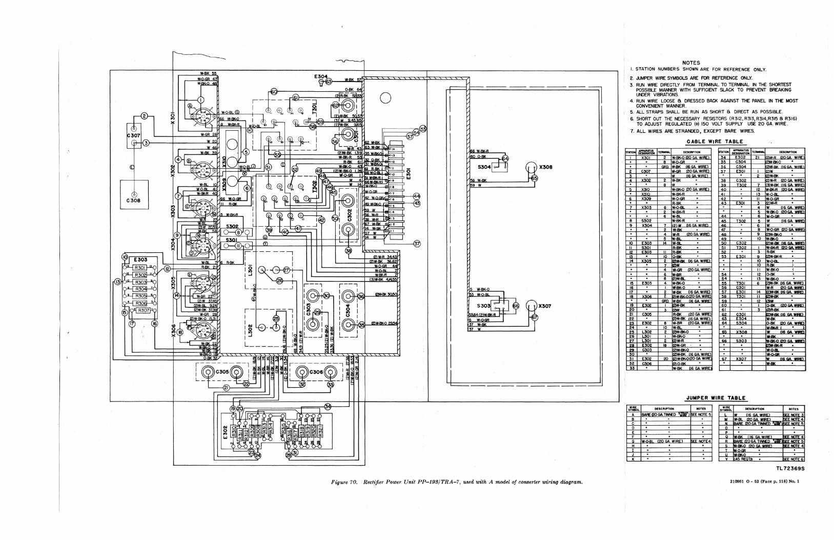
o ---, I
X308
________ J
Figure 70. Rectifier Power Unit PP-193/TRA-7, used with A model of converter wiring diagram.
NOTES I. STATION NUMBERS SHOWN ARE FOR REFERENCE ONLY.
2. JUMPER WIRE SYMBOLS ARE FOR REFERENCE ONLY.
3. RUN WIRE DIRECTLY FROM TERMINAL TO TERMINAL IN THE SHORTEST POSSIBLE MANNER WITH SUFFICIENT SLACK TO PREVENT BREAKING UNDER VIBRATIONS.
4. RUN WIRE LOOSE a DRESSED BACK AGAINST THE PANEL IN THE MOST CONVENIENT MANNER,
, 5. ALL STRAPS SHALL BE RUN AS SHORT S DIRECT AS POSSIBLE.
6. SHORT OUT THE NECESSARY RESISTORS (R312, R313, R314,R315 S R316) TO ADJUST REGULATED (+) 150 VOLT SUPPLY USE 20 GA. WIRE.
7. ALL WIRES ARE STRANDED, EXCEPT BARE WIRES.
CABLE WIRE TABLE
IsrAT10N APPARATUS mlMlNAl DESCRIPTlON !;rATIOOI APPARATUS
TERMI"" DESCIOPTION DESIGN.<TION DESIGNAnON
i I X30 2 W-~ l!20 GA. WIRE 34 E302 21 II2lW-R 120 CiA. WIRE
" II IW-O-GR " 35 C304 12JN-BK-O · · Iiiin IW-BK 116 CiA. WIREl 36 C304 I2IW-RK 116 GA WlllFl 2 C307 W~R 120 GA. WIRE 37 E301 I ~lW · ~ " Iw 16 CiA. WIRE . 2 121_ · 4 X30? 2 W-BK 38 C3C2 12Iw-R !20 GA. WIRE
, · 8 W " 39 1302 7 1131W-1lK 16 CiA. WlRE1 , 5 X3IO W-BK-O (20 GA. WIRE '40 12 Iw-I!K.R 120 GA WIREI , " -iGio W-BK-R 41 13 IW-O-BL
.Ii X309 w-O-GR " i 42 II IW-O-GR · , " '_RIC · 4 E301 3 11?1W-R · 7 X"O" R W- ,-81.. " 4 W '16 ('.A. WIRFl . · ? W-flK.R , 5 1_ 120 GA WlRl'1
· 6 IW-Bl " -'l4 6 1",-"-,,,> · 8 5302 W-BK-R · 45 T302 5 W 16 GA. WIREl 9 )(304 7 112lW tltiGA.wJBEl AS. 6 Iw · , , ? I_I( , 47 8 w.o-GR 120 GA. WIRE ,
" 4 IW-R 20GA.WIRE1 411 " 9 I?lW-RIC.ll · " 5 W-BL , 49 10 '-IlK-
10 E3l3 14 I\\LBL 50 C302 121W-1lK 116 GA. WIRE)
II 5301 R-BK , 5J T302 I W-BK-R 1M GA WIRFl 12 E303 II R-BK 52 3 R-BK ,
1-. · In -IlK 53 E301 9 12lW-1lK-R · 14 '30" 2 1121_ U6 GA WIREI " 10 W-I-BL · '7 I2IW · · 10 R-BK , · 4 \\LGR 20GA WIREl · II W-IlK.Q
I-
· 6 l-BR ..5.4 12 0-1lK , , 8 I2lW-BL 54 13 -RI<.O · 15 E303 4 W-flK.0 , 55 nOI 6 IW-BK 16 GA. WIREl 16 I W-BK-O · 56 C301 -R 120 GA, WlREl 17 · 2 W-BK 16 GAWIf!El 57 E301 14 2- 16 GA. WIRF' III 'II""'" 2 I2IW-BI(.Q{20 GA. WIREl 58 T3CI II - · ,
GRD. W-1lK 116 GA. WIREl 59 12 IW , 19 E302 I I2lW-IlK · 60 I -IlK 120GAWlREI 20 3 C2IW · 61 3 I2IR-BK 21 C305 R-BK 20 GA WIRE _62 C301 12lW-BK 116 GA. WIREl 22 " 121_ 16 GA. WIRE 63 E3C4 W-1lK · 23 E302 .8 W-BR 20 GA. WIRE 64 5304 0-1lK !20 GA. WIA£) 24 ·
If. " W-8KR · 25 L302 65 )(30A W 'IS ('.A W~
26 L301 · I- · 27 L301 2 K2J\\LR " 66 5303 Iw.BK-O l?0 GA WIAFl TA E302 18 IC2IW-GR · " ~ · ?CI C303 1(2)W-8K.Q · · . IW-O-BL · 30 k2l_ 116 GA WIRE " 1W-n.r.R · 31 E302 20 1121W-8K.Q12Q GA WIRE 67 X307 Iw 116 GA. WlREl 32 c.~ 1(2)0-1lK · . IW-BK 33 W-1lK 16 GA. WIRE
JUMPER WIRE TABLE
WIRE DESCRIPTION NOTES WIRE DESCRIPTION NOTES SYMBOL SYMBOL
. A BAREI20GA TINNED '''IW' ISEE NOTE 5 Iw 116 GAWIREl !SEE N<ITE -jj
" M IW-BL !20 GA WIRE ISEE NOTE 4 C · IBARE 120 GA TlNNE[ 'll.1IlI' !<:FF' Nnn:5
i 0 · . . E · . . . F · GA. WIRE !SEE NOTE G h",tu>1 20 GA. WIRE !SEE NCTE4 BARE 120 GA. TI~D "J.1lI'l I<:FF' NlTI'F' 5 H " . S I-~ I?O ""-.WIRF' !<:FE NOTE 4 I I-O-GR J . U ~~ . K · V AS REQll) BEE NOTE 6
TL72369S
210961 0 - 52 (Face p. 118) No.1
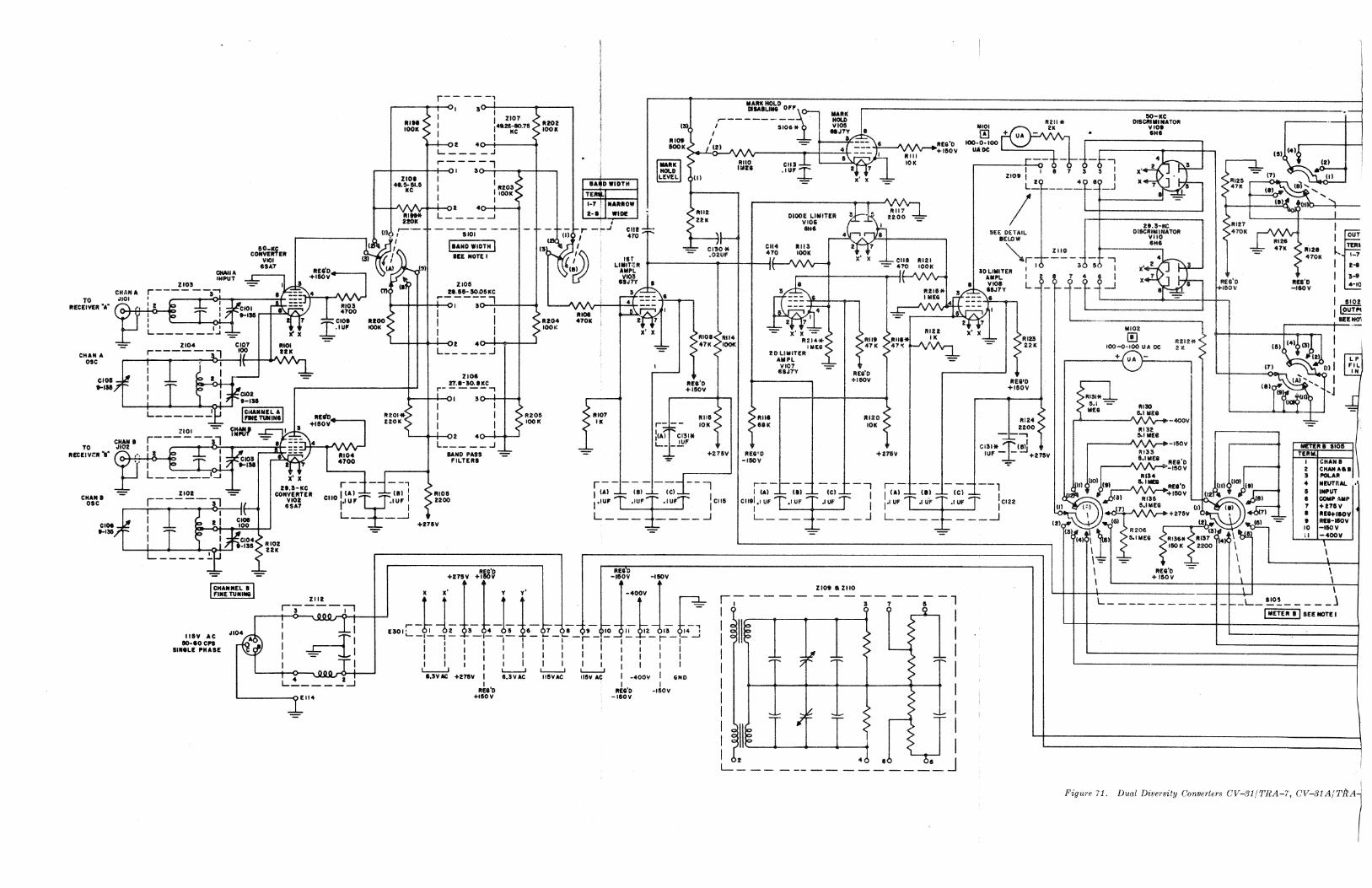
TO IlECEIVlIt "A"
CHAN A DIe
CIDe 1-111
TO R!CEIV:!II""
CNANI OSC
CIOI 1-1111
CIWIA INPUT
r-- ---, ~----~~ s·o-+-----~----~
1101
I.AND WIDTN I lEE NOTE I
ZIOII n.1I11- SD.DIKC
..... -----.., ~_1~~~_o1 So-~I~--+--1
I I I I
ZIOI 27 •• -so.IKC 1"'-----,
+-_1-+-0 I so-4-+--+
'---4-+-02 4o--+--+-..J
r- --,
L _____ J
BAND PASS FILTERI
112011 lOOK
Itl~ IX
r------- ---,
DIOOE LIMITEIL VIOl 8111
CII4 IllS 470 lOOK
)C' )( -= 1t214*
IIiEG 20 LlIlITEIt
AMPL VI07 IIJ7Y
Rill 11K
x' )C CIII 1t121
Itlll 47K
REI'D +IIIOV
11110 10K
-= 470 lOOK
+271V
II.a-KC CONVERTER
VIOl lSA7
I'A' (II I CliO I,IU'UIUF :
L __ ±_.-J 111011 2200
+17IV
I (A' 'II ,e' I I".UF T ,IU'f ,IUFT ICIIII L _______ -.J
IIiV AC BO-IOCI'S
IIIIIU PNAII
It 102 22K
,..----t--()-r '---,.ZII0200 - r-< t:)-+-4...-J~ 'H,::h J:Ir 1. L ~ _ ~ -r' _ ~I1.1~ k I I I I I I I I I I I I
L-------oE 114
I I I I I I I I I I I I I I I I I I I I I I I I I I I I I I I I I I I I I I I I I I L--...J '----I 1...-.-1 '----I
1.5VAC +Z7IIV I e.3YAe 115VIIe lillY Ae I -400V I 'NO
II~'D .. ...\"0 -I~OY +1110 V -IIOY
r;-- -- ---I I I I I I I I I I I
ZIOI .. ZIIO
-;--7---;- -1
I I I I I I I I
o 11211*
100-0~:00 ~UA - 2K uADC
-- -ZIOI: I • 7 S
L~ 4
/ SEE DETAIL
.ELOW
'\.r ZIIO
I II -, I liD LIIiITER I I
AIIPL I
l.KJ:v L ::=4l='~_ .... 1t::1;;_~._,-,--I-------~-=--_+-~+RE....,III~~ Itn'D
-fIDV
OUT TElla 1-7
1-1
a-l 4-10
I 1101 I IDUTI'I
KINOl
RIU 22K
IIE8'D +IIIOV
11124 2200
---, elSl* 1',~
IUF T +275V
11102 [!]
100-0-100 UA DC
r-----'+~ UA t------,
11152 1101111.
r----J\.A''''~_-IIIOV
II lIS II.IIIEI
(II
-
TlEIt I 2 I 4 I
• 7
• I 10 II
It. 11011
CHAN .•
LP 'IL IN
CHAN A ... POLAII N!UTI'IAL INPUT 00II, AIIP +171V 1t!"'IDY 1tD-IIDY -1110 V -400V
\ \ \
_L_ !!.D~ _____ ) IIiETER • I lEI! MDTE I
Figure 71. Du", DW, .. ity Conooo1, .. CV -31/ TRA -7, CV -31 A/ TRAJ
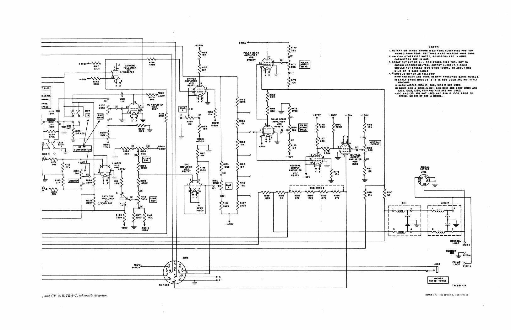
---"-
+27liV RI40V
22011 2 FOLLOWER I ~A CATHODE
I VIII .-----------11-4 --- 11/2111L'7tT
.~ -IIIDV
RI42 550K
RI41 4'701(
+275V
DRIVER AMPUflER
<-- RIIiI ~'811 <
«~RIG7 >Z2K
~
iEviiii:
~~lv/-~' r"it :=:. '--
~-+4~l ....-----------l" A A A REI'D
x x' -=_ IORMAL
'ARI( I ItItD'7 <> IZ) • 4 .tC AMPLI"ER
III ~\~~ ~i:+l1IOV ~ \ ! I 211EI ").,t--.:o-f':r-I~ - - _f nOQ1-
CIZ' :::: i== U-tJ SI04 5' I I":S II<ZI
III Jt.. A 151 RIlIIS 10K
VVV RllllI 2K ~~ ~~O.~ I 121 I AV' Av )-
II'H ~CII7 <"R11I4 - "",'000 > 11101 <.,>' 11111 LA A A _ ..L . <;'RI511 > 1100 _
r ~~,v- -=- <;. 2.Z MES RIIO ~
REI'D +lIIOV
III 27011 CIZI ~ - - ----'-IICl~-f---- F +'l:~ ~_~IOO ItEt'o n. t-.. DRIFT I -IIIOV ~Ul A A (5) IIEI'D
\ ..L COMPENSATOR I 1111' "yUR·,":-'"4-o--..... + HIOV > _ 1105 0 0 =- I 5n (2) 5011 $~::: -
GIll <..11148 II •• VIII >RIU D-C ). S 2711 ~ I IHI <:> IIOK AMPLIFIER <:> 11111
<Ii R:'~ ; I -r.1+I•IIV < t~~~T <;"OOK
.-----~ '<---I~ 4 ~--------~--~----~ ~
+27l1V .. ----...... -------. ~ RI70
35K I'OLAR MARK < AMPV~~ER 5 9(5)
~ 4~11Z1 ~:::~
> RII2 5110K
<.,.11111 S IIIK
I ••. +' Am x' x -= V
(»11118 <;. 820
<
~RI7Z ~ 10K
11111 ~1I1'75 ltD ~ :>4'700 - .,
'-----1 POLAIIPACE < 151 AMPLIFIER
__ ~IV"TY <:>111'74 T 1((:1I:t:.... • VIII > fit I
II ----f:--<l-KIIOK _CE +---< +-1r=-\+..=-=-=- 121?,
I '7 I -
+27I1V! -4rV -ISOV -I~OV
,
~IIIIO ~II1I5 <;'11171 < 15K < 220K < 1011 > . > > <
y' v III
>11114 11K
<111111
S'lK .,
V y' ~Ul - ~II1711 -ISOV <;. 10K
\ -ISOV
~R;77
~~~ I RI'71 1 ___ 2201(
4 ---L-__________________ +-~II~, I
zn7 -=
It 1t I ). III£'l..'lrTLI I~ t\. III <Rltl
B:.::~ > 1101(
• /IIEUTRAL .. OUTPUT =- AMPUfll1i III
VIII eves
<Rill <) 10K v' Y <>RI'7t
NEUTRAL OUTPUT
AMPLIFIER VII7
IInv -IIIOV
I <:> 1011
i,'v~v >. '<1 ~ LI:I~ER <> I\~'lpi I--
II ----- > 7 2 -). > ;H E=" RUIO I LlMITERI RI4~<> -R141 ~ «> R III 2 1.f5 RItO > )-,
17K )Ul 2tDII? x ~ -:> <- 4'7011 --'J_~ __ ~"I_+J4~H-<IIOO>-" .. :<~> I MAS I < ~::
< ~
1'0 ~V
~,-. (2) > I ~ RI55v ~(5) 5'7 II .IK a ~II "-
CATHODE III <: R14f5 ~ • (II I • <» FOLLOWER .7 f500K COMP V V
R 15 V III --- I > AMP '---Z10K~ (l/211SL71T ? < <>RIII
J ~ RE.o ~IMII -IIiOV <
RI45~ nOK
1114'7 (»11141 2200 <;. HIOK
J\IV\r JV\tvo Rift lUll _ 50
,...-------1'""-----, I III NOTI I ~i
.J\I\r -'\, "" ~ -'\,A;,/\r RII7 RIM Rill RI14 170 170 & 70 Z70
< <~RI" ~aoll
NOTES L ROTARV SWITCHES SHOWN IN EXTREME CLOCKWISE POSITION
VIEWI:D fROM RI:AR. SECTIONS A ARI: NI:AREST IINOI ENDII. Z. UIILE 1111 DTHI:RWIIII: IIOTED, RE515TOll5 ARI: III OHMI,
CAPACITORS ARI: 1M UUf. 5. STIIAP OUT AIIV OR ALL RI:SIIITORI RII4 THRU RII7 70
OITAIII CORRI:CT IIEUTRAL OUTPUT CUIIREIIT. CIRCUIT SHOULD NOT I:XCI:I:D liDO OHMII IEQUAL TO AIOUT DIIE MILl: Of II IAII: CAlLE) •
4. II MODELS DIFFER AS FOLLOWS: Rill AIID RIOI ARE lOOK 1M MAVV PROCURI:D IASIC MODI:LS. III I:AItLV IASIC MOOI:LS. ZII5 IS IIOT USI:D AND RI" IS S.1
MEGOHMS. IN IAIIIC MODILS. RIM IS 11011, SlOI II NOT USIID. III Msic AIID A MODELS, R211 AN.D Rill ARI: 1400 OHMS AND
EIII. EI25. EII4. R214 AND R2111 ARE NOT US liD. CI50 AND CISI ARI: NOT USID AIID Rill IS 10011 PRIOR TO
URIAL 1I0.tD5 Of THE A MODIL.
IIIIIAL OUTPUT ~ID5
~ ZIII r-------,
iJ.. 2' i
1 Tnl I I
ZIII*
r----f-' I ',00 I I
I hi I I -ISOV IIEI'O
~IIDV
I T -I '-__ ~----------------------_+------~------4_~11~5~.~n l~ - I
I T -= I I I ,000 4 I L_=-____ J L ______ ...J
~IOI
REIIO:_-----Ihc...~.Q., 1; ~ ~IOI
IIIUTRAL LOOP 1114*
COIlIIOII tllO~ -= 1111*
POLAR 0-LOOP 1111*
+IIIOV (E 0 A\ AU o~ LIA~~~--------~--------------------------------------------------------_4----------------------------------o-~
--------------------------------------------------4\-b~~ ~ JO~~J~----------~x W,O / x' I PHOIIES 1 ~
TO P405
IIEYED TOilES
Til III-II
, and CV-31B/TRA-7, schematic diagram. 210961 0 - 52 (Face p. 118) No.2
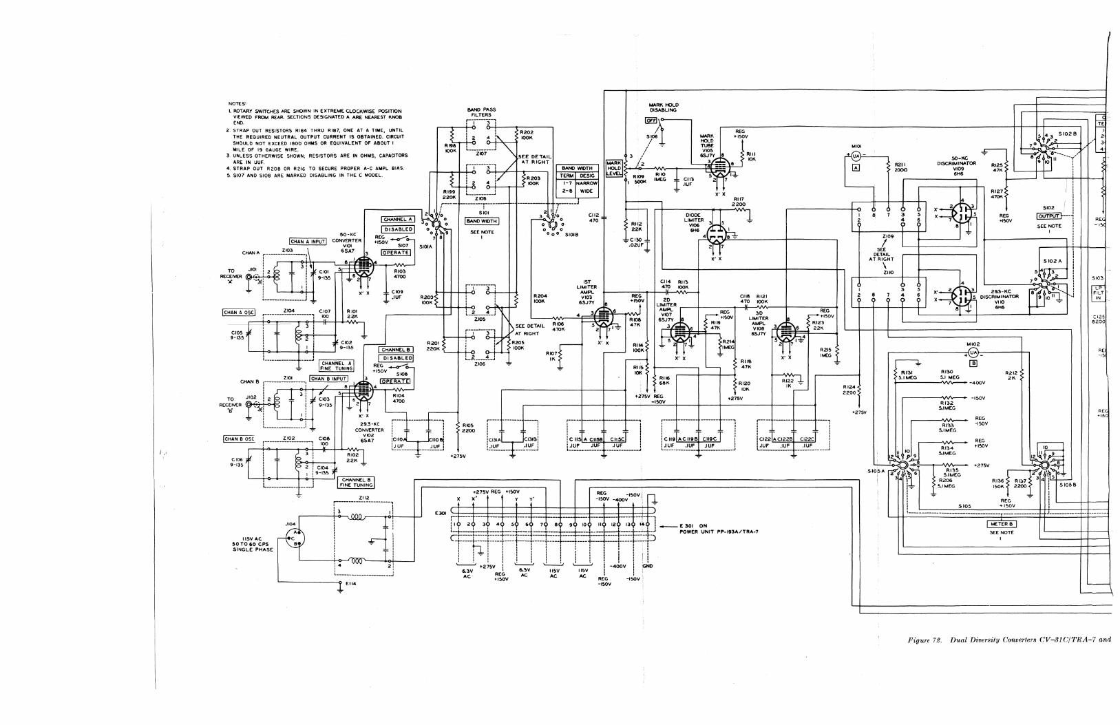
NOTESO
I. ROTARY SWITCHES ARE SHOWN IN EXTREME CLOCKWISE POSITION VIEWED FROM REAR. SECTIONS DESIGNATED A ARE NEAREST KNOB END.
2. STRAP OUT RESISTORS RI84 THRU RI87, ONE AT A TIME, UNTIL THE REQUIRED NEUTRAL OUTPUT CURRENT IS OBTAINED. CIRCUIT SHOULD NOT EXCEED 1800 OHMS OR EQUIVALENT OF ABOUT I MILE OF 19 GAUGE WIRE.
3. UNLESS OTHERWISE SHOWN; RESISTORS ARE IN OHMS, CAPACITORS ARE IN UUF.
4. STRAP OUT R208 OR R216 TO SECURE PROPER A-C AMPL 8IAS.
S. 5107 AND 5108 ARE MARKED DISABLING IN THE C MODEL.
CHAN A r-------~~~---1 ! I
TO JIOI I RECEIVER (O)~-oj->+' _~
''';
ICHAN A osci
CIOS 9-135
CHAN B
ZI04 CI07 r-------------------, 100 RIOI 22K
I CHANNEL A I I DISABLED I
I ClOg .IUf
RI99 220K
BAND PASS fiLTERS
-3"-1 I R202
4 i'\. lOOK
_oj '" SEE DETAIL
'3i / AT RIGHT
~ i / {R203
04>-ti'_-t--t_.l~· lOOK , , ~ ________ .J
ZIC8
BAND WIDTH
TERM OESIG
1-7 NARROW
2-B WIDE
_ _________ ; _____ J
SIOI
I BAND W-ID-TH--'I
SEE NOTE I
2 I j
~~o: °0° SI018
~RK HOLD EVE
RI09 I 500K
RII2 22K
t.lARK HIOLD DISABLING
t..IAAK HIOLD TUBE VI05
6SJ;~=~ 6
REG "'ISOV
Rill 10K
RIIO I IMEG r :!: CII3
.IUf
5 1-2 7 .
x' x RII7
2200
DIODE ,& 'I LIMITER 3 5 "* VI06 6H6 I
SIOIA
_ CI3Q
- •02Ufl rn41 ....... 8 .,.
2 7
R204 lOOK
RI06 410K
1ST LIMITER
AMPL V 103
6SJ7Y 8
3F=~6
· '~fh REG +I~V
t Rloe 4711: 1\ SEE DETAIL
t-_+--lf_°-o-'-----4 ~V AT RIGHT
R201 !/ R205
220K LR ___ tr"""; lOOK
ZI06 .,.
RIO~r X' X RII4 _ 10dK II'. _
RII5 10K
CII4 RII3 4TP lOOK
" 20
~ t'W RII6 681'.
x' X
r-~~~v RII9 471'.
f~214 I MEG
'---
CIIS RI21 4;,0 lOOK
3D LIMITER
AMPL V loa
6SJ7Y
RIIS 47K
RI20 10K
TO RECEIVER
ott
>275V REG -ISOV
'tZ75V
ZI02 CIOB r-------------------, 100 ICHAN B osc
CONVERTER VI02
6SA7
r----- ------- -----, , , , , leliO 11081 , ,
RI05 2200
r---- ------.±-.----: , , : CI31A CI31 a!
r----- ------ ------- ---., I t , : !CII~ A CII5B CIISC :
r----- -------- ------- ----, ,-----, : ! 'F
, , 'F , ! :: , , I ell9 ACII9B ClllIC : I CI22
I.IUF .IUF .IUF I IJUF
REG
Wr-+ISOV IW ~:; 52 7 I .,.
R215
X' x IMEG
RI22 ..b IK .
-
-------- ------- ---, , , F 'F I , ACI22B CI22C !
.IUF .lUF I j~! L~~~ _____ -=- __ .:~~~-I
:~: !;~~--- .,. ---~~~j L:~~ _____ :~~_ __ ~~~!: _____ J L ____ o ______ ___________ .J L ____________ _____________ ..I
el06 9-135
115VAC SO TO 60 CPS SINGLE PHASE
ZII2 r---------------------, , , , , .-------t-: -c3~ I : E30I
! 4 2! l ______________________ J
EII4
+275V
+275V REG +ISOV
x x' Y'
• it- --~- ---3 ---; --;r~l-;- --~ ---; --~ ---1~;r-~~ -~t -1 t-t----l.----:~:=:i::::J::=:t.====:+-t' ===:r==i==±:::.:-r:.::=t:.:::-r:==t=~ C..L,-::::t::: I I I I I I I I I I I '1-1
T -r-----r----t---1-----r----+-----t ----;----1-----r----t-~-r I ill ! I ! ! ! ill : I ! I ! -:-! ! 1 I ! ! I ! i ! i!! '-----' +2~~V i ~ ~ ~ i -400V il eND
6.3V RE~ 6A~V IISV IISV 1 I AC >ISOV AC AC REG -ISOV
-150V
_E301 ON POWER UNIT PP-193A/TRA o 7
.,.
5 43 S 102 B
MIOI
r±@r-=---.., R211 2000
~ SO-KC
DISCRIMINATOR
o\: P 2
~~-~--- ' 8 11--( 9 10 : o
RI24 2200
I 2
I 2
+21':#
RI25 VI09 47K
I ! 6H6
: , RI27 : 410K : ,
~~ SI02 ! , , REG I OUTPUT r---, +ISOV
B I SEE NOTE ! I
g 7 3
* 8
? 6
j09 SEE
DETAIL SI02 A AT RIGHT
\ ZIIO
3 5 e 7 ? ?
I ~~ X' 2 3 29.3-KC X 5 DlSCRIM INATOR
7 VI 10 B ~I 6H6
I
MI02
r-----------------~+ UA.}----------t-,
RI31 5. I I\.1£:G
1'.130 5.1 MEG
[!]
~-----------JVV~--~-400V
RI32 5.1 MEG
-150V
REG
I R 3 -150V
~5'I~iG REG
+150V
..,-'-___ ~"<12 ... ~1i1 ~ 9 8 5.~~~ SIOr;A ~ \~ 5~:JiG
34 )1. R206
1'-:- 5.1 MEG
I .,. SI05
+-215V
R212 2K
12~ ,.-_--.!o. ...... Lf<>.;!l~~~
RI36 RI:'76f3 /\h~ 150K 2200 ! S 105 B
-:- ! REG :
+ISOV I
,
'""J r.rE fJ
2 3
~
REC -'5
5103
~p
FILT IN
;:125 8200
RE -IS
REG +150
}
t____________________ --------------T------------- J ____________ _____ _
I "'E~ER B I
SEE NOTE I
-
Figure 72. Dual Diversity Converters CV-31 C/TRA-7 and
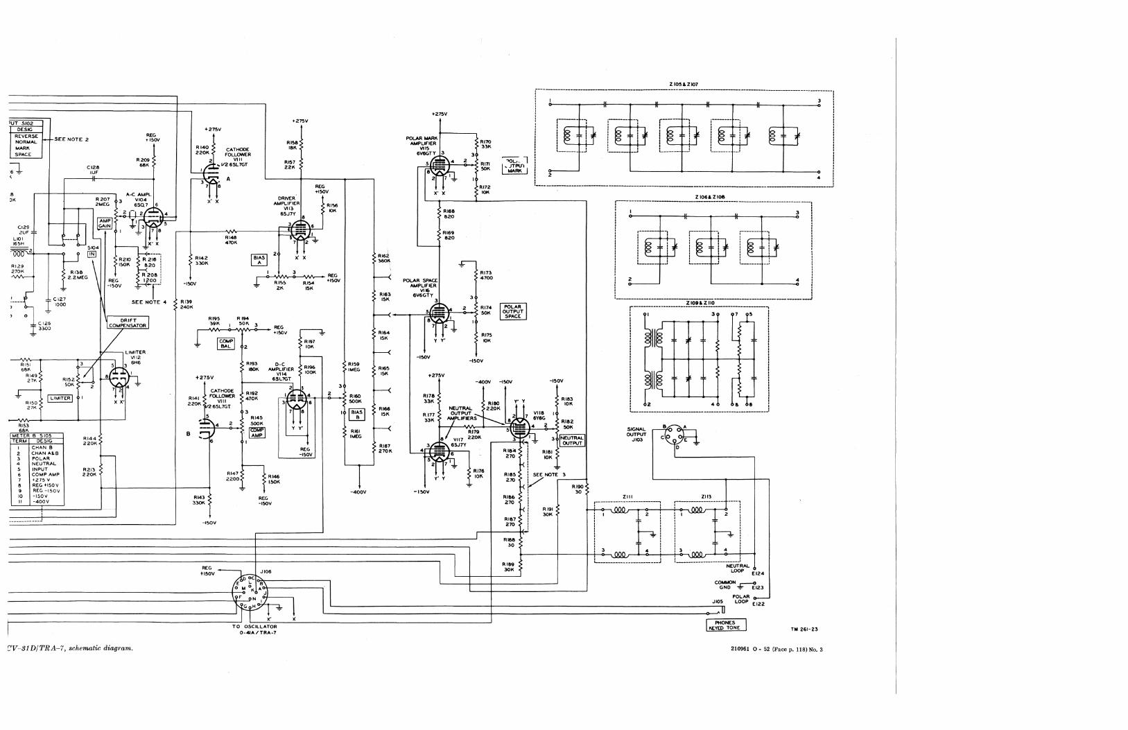
'UT 5102 DESIG
~~VRE:;C i- SEE NOTE 2
MARI\ SPACE
.8 ~K R207
~_o-~ZMEG
REG +ISOY
R200 68K
A<' At.APL
+ 275V
RI40 2201\
CATHODE fOLLOWER
2 VIII I ?-..: V2 6SL7GT
+27SV
RI!>!! t8K
RI!H 221\
11-;8 A
3 VI04 X' X ~~~R
2 I-I 2 r- 4 6SJ7Y
REG +l5OV
RI56 IQI(
6So.:"'~6 VII?>
..... -- II
~~~: U l~~1 I 113~5 ~~ L/OI ~__ L It r r--+------'lR"I48./'r------+~---'34-7 2 ~~ 165H ~ 5104 ~ j:X' X 410K
RI29 1501\ U20 I ,30K
--,,2+----..,U [@\IN R2/o 7z-1~-1 RI42 18~1 2 x· ! ~7.?.!' R138 'RZOII ! .--oI-'lMI'v-... 3>-.JVV'v_ REG -vvv-- 2.2MEG REG ): -.200 ! I +ISOV
~ -150V ~r -15QV ~ ~~5 ~~
r CI27 SEE NOTE 4 1000
° CI26 .J 3,00
RI51 5BK
RI49 271'. RI52
50K
~ I LIMITER I RI50 27K
~'i~ METER B 5105
ERM DESIG I CHAN B 2 CHAN ALB 3 POLAR 4 NEUTRAL 5 INPUT 6 COMPAMP 7 +275 V 8 REG +150V 9 REG -150V 10 -150V II -400V
, -------------
Ef 2
I
RI44 220K
R213 2201\
~ DRifT I I COt.APENSATOR I
LIMITER Vll2
5 3 6H6
I 8 ,p
7 2 4 ":"
XX'
RI39 240K
RI95 RIM ?>9K I 501\ 3 REG
~ I +ISOV
I~I R197 2 10K
t---R193 D-C I80K AMPLIfiER RI96
lOOK +Z75V
CATHODE
RI41 roLLOWER VIII 2201'.
V26SL7GT
B
-:'~4 q:
R143 330K
-150V
2
RI47 2200
VII4 6SL7GT
it l 'RI901 ,-1 ~4 4701\ 3i'f16 3 7 8
RI45 5001\
:1=1
y y'
'---I
REG -ISOV
RI46 150K
REG -150V
t~v~ JI06 oc:::-'
3
2
I
RI59 IMEG
RI60 !lOOK
I~SI RI6I IMEG
R163 151\
RI64 15K
I--< R165 15K
RI6f 15K
RIB7 2701\
+27SV
POLAR MARK RI70 At.APUrIER
VI 15 ·331\
~~4 3
2 'Rill 501\
821~ 1
11172 X' X 10K
RIM 820
RI1I9 1120
'---
~ Rln
POLAR SPACe 14700
At.APLlriER VI 16
eV6GTY 3
M~ 2 RI74
'501\
I
RI75 Y Y' 10K
-15OV -150V
+275V -4QOY
I
I
~l I dTPITl I MARl<.
I POLAR I OUTPUT SPACE
-ISOV
RIBII 30
RIII9 30K
2105&2107 j-------------------------... -----------------------------------, , I i I I'" 3 I
" ! !
I f
r---- --. i ' i ~ ~! + I , , '--___ -..I
, -, ,---h ' -:
I~, it i~*!+ I~: it L. _____ J L_~ l ____ J
I 2 4 II: i .--------------------------------------------------~
-I50V
ZI06&ZIO& ~------------------------------------J
al~----~~----;~------r_-----l"._----_1--- 3! " .. ---.., i ,----- 1
11,1 ~ ,P ! , , L ____ J
Z
r--- -, :,:, ~ I
F I r--- I..,
I ~: L __ _
I ! 1-'
I i I
4 I -----------ZIOtL ZIlO-------------------..J
r-----------------------------------------. I I 3 7 ~
I I
I II :1: '- :
I
i I II
: r-
! I 2 4 a I '--------_ ... _-------------------------------"
SIGNAL OUTPUT
JI03 ~A
C E D ~
ZII3
r------'----- ---, ! I 2 ;
! ~I 13 ,oon f 4 ! ,~ , I _________________ J
NEUTRAL LOOP EI24
~~IZ3 --------------------------4-...:0'" 1\ A~ : ~ B""----~---------,·l POLAR 0-LOOP EI22 __________________________________________________ ~~f GO: I~--~--~ L __________________________________ -+ __________________________________________________ J_IO".~
ox; ~ I .PHONES I TO OSCILLATOR KEYED TONE
0-41A/TRA-7 r TM 261-23
C'V-31 D/TRA-7, schematic diagram. 210961 0 - 52 (Face p. 118) No.3
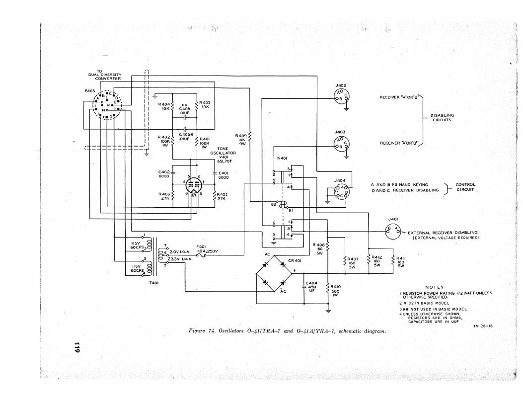
... ...
.g
TO DUAL DIVERSITY
COI)IVERTER
P405 I_- oor '''''s ect"_,
IA L 0' r---t-e K· Ee\ I :J'. M~ ~N~
, I ' "o':!aGt/
,'I IT i
I
::~ : I R404 I I 10K
I I I I I I
'I
; ,,~
J(J(
C405 .01Uf
"
" ,rC403)( .01Uf
R403 10K
J402
tAO" I~i
J403
'Afi"
RECEIVER ",o/'OR"B"
DISABLING CIRCUITS
~:t=::t=I=
\1 _~-+ __ , I
--~
R402 lOOK IW
R401 lOOK IW
R409 4K 9W
TONE OSCILLATOR
V401 6SL7GT
~B! RECEIVER ""OR"B'
C402..L 6000 -r
..L C401 -r 6000 fitlz
4 I
R406 6 7 3 R40~ 27K 27K
115V II 7 60C.PSZ G:. 2.0V 1/4A
F401 I.OA,250V
3
115V ~ 60CPS4 ~
1~4A 5
T401
'-'
1\401
~I I 4L-1--I I
6B- A-P 'Y-06T
I I
~ B 0 C
A AND B FS HAND KEYING
o AND C RECEIVER DISABLING )- CONtROL CIRCUIT
~II h 9 S 4:J '~ 0 - EXTERNAL RECEIVER DISABLING (EXTERNAL VOLTAGE REQUIRED)
... ,R408 160
J401
>C ~+~', ' I t f 1
~AC
'f>W R412 ~ R411
160 160 'f>W 'f>W
,R407 160 5W
... C404 r 450
Uf
...
R410 .560
IW
NOTES
I. RESISTOR POWER RATII'iG 112 WATT UNLESS OTHERWISE SPECIFIED.,
2 )( 02 'IN BASIC MODEL
3.)(* NOT USED IN BASIC MODEL 4 UNLESS OTHERWISE SHOWN,
'RESISTORS ARE IN OHMS,. CAPACITORS ARE IN UUF
T,M 261-16 Figure 74. Oscillators 0-:41/TRA-7 and 0-41A/TRA-7, schematic diagram.
;~
. '" 'i .~
1 , J
INDEX
Paragraph Page
Adjusting relay _______________ _ 50-54 69-75 Alinement:
Converter ___ c _______________________________________________________________________ _ 55, 56 76, 78 Power supply __________________ : ____________________________________________________ _ 57 81
BIAS B controL ________________________________________________________________________ _ 28b 28 Block diagram:
Converter _________________________________________________________________________ _ 23 21 Converteruse _______________________________________________________________________ _ 4a 2 Power supply _______________________________________________________________________ _ 33 38 System _____________________________________________________________________________ _ 22 19 Tone oscillator ___________________________ c __________________________________________ _ 33 38
-~
Burnishing relay contacts _________________________________________________________________ _ 50c 71
Carrier control mark-hold circuit- _________________________________________________________ _ 30 33 Channels, theory ________________________________________________________________________ _ 24 21 Checking:
Discriminator _______________________________________________________________________ _ 44e 49 Drift compensator _~_ _ _ _ _ ___________________________________________________________ _ 44g 50 Forshorts ____________________________________________________________________ ~ _____ _ 43 47 Input circuit ________________________________________________________________________ _ 44c 47 Limiter ____________________________________________________________________________ _ 44d 48 Mark-hold circuit __ ~ ________________________________________________________________ _ 44i 51 Ou tpu t circuit ______________________________________________________________________ _ 44f 49 Relay _________________________________________________ ~ ____________________________ _ 50-54 69-75 Tone oscillator ______________________________________________________________________ _ 44h 51
Cleaning relay __________________________________________________________________________ _ 50b 69 Code, TT ______________________________________________________________________________ _ 18 16 COMP AMP controL ___________________________________________________________________ _ 29d 31 COMP RAL controL ___________________________________________________________________ _ 29d 31 Compensator circuit, drift __________________________________________________________ - - - - - -- 29 31 Contact adjustments, relay ______________________________________________________ - __ - - _ - - -_ 53 74 Controls _______________________________________________________________________________ _ 8 4
Daily maintenance _____________________________________________________ - ___ - - - - - - - - - - - - -- 12 10 Data, technical _________________________________________________________________________ _ 5 3 Demoli tion ____________________________ - - - - - - - .- - - - - - - - - - - - - - - - - - - - - - - - - - - - - - - - - - - - - - - - - - - 74,75 92 Description ___________________________________________ -----------------------------------Differences in models ____________________________ - _ - - - - - - - - - - - - - - - - - - - - - - - - - - - - - - - - - - - - - --
6 3 7 3
D-c output circuit __________________________________ - _ - ___ - - - - - - - - - - - - - - - - - - - - - - - - - - - - - - -- 31 35 Disabling circuit _____________________________________________ - __ - - - - - - - - - - - - - - - - - - - - - - - - ~ 39 44 Discriminator:
Checks _________________________________________________________ ~ ___________________ _ 44e 49 Final tests _______________________________________________________________________ - __ _ 66 85 Theory ____________________________________________________________________________ _ 26 25
Drift circuit: Checks ____________________________________________________________________________ _ 44g 50 Final tests __________________________________________________________________________ _ 67 -85 Theory _________ ~-------------------------------------- _____________________________ _ 29 31
Driver circuit- _______________________________________________________________________ - __ _ 28 28 Emergency keying _______________________________________________________________________ _ 38c 44 Forms ________________________________________________________________________ ~ ________ _ 2 1 Frequency drift circuit ___________________________________________________________________ _ 29 31 Front panel controls _____________________________________________________________________ _ 8a 4 IIand keying _______________________ c ____________________________________________________ _ 38e .44 IIeater power supplies ________________________________________________________________ -_ -_ 37 42
120
Input circuit: Paragraph Page Power _________________________ c ___________________________________________________ _ 34 38 Signal:
Checks _________________________________________________________________________ _ 44c 47 Final tests _____________ -~ ______ c _________________________________________________ _ 63-66 84-85 Theory _________________________________________________________________________ _ 24 21
Limited storage_ ____ __ _ _ _ _ _ _ _ _ _ _ _ _ _ _________________________________________________ _ 72, 73 92 Limiter ampli:f\er circuit:
Checks ________ ~ ____________________________________________________________________ _ 44d 48 Final tests ___________________________________ , ______________________________________ _ 65 85 Theory ___________________________________________________________ ~ _________________ _ 25 23
LIMITER controL ____________________________________ c _________________________________ _ 29f 33 Linear discrimina tOL ____________________________________________________________________ _ 26 25 Low-frequency shift tests ____________________________________________________________ . ____ _ 70 88 Low-signal input tests ___________________________________________________________________ _ 69 88 Lubrication ____________________________________________________________________________ _ 13 13 Maintenance:
~aily __________________________________________________ - ___________________________ _ 12c 13 ~esert _____________________________________________________________________________ _ 14d 14 Monthly _____________________________________________________________ cc ____________ _ 12c 13 Relay _ _ _ _ _ _ _ _ _ _ _ _ _ _ _ _ _ _ _ _ ___________________________________________________ _ 50 69 Weekly _______ -' ___________________________________________________________________ _ 12c 13 Winter _____________________________________________________________________________ _ 14c 14
Mark-hold circuit: Checks _____________________________________________________________________________ _ 44i 51 Theory _________________________________ . ____________________________________________ _ 30 33
METER B: Checks _________________________________________________________________________ .. ___ _ 44i 51 Theory _____________________________________________________________________________ _ 32 313
Metering circuits _______________________ . __________________________________________________ _ 32 36 Methods of destruction __________________________________________________________________ _ 75 92 Model differences _________________________________________________________________________ _ 7 3 Neutral:
Currents ___________________________________ -________________________________________ _ 17b 15 Signals _____________________________________________________________________________ _ 31c 36
Operational check _______________________________________________________________________ _ 44 47 Organizational:
Equipment ________ : ________________________________________________________________ _ lOa 10 Too~ ______________________________________________________________________________ _ lOa 10
Oscillator tone circuiL _ _ _ _ _ _ _ _ _ _ _ _ _ _ _ _ _ _ _ _ _ _ __ _ _ _ _ _ _ _ _ _ _ _ _ _ _ _ _ _ _ _ _ _ _ _ _ _ _ _ _ _ _ _ _ _ _ ________ _ 38b 43 Output circuit:
Alinement __________________________________________________________________________ _ 55d, 56d 7.8,80 Checks _______ c ________________________________ -------- ________________________ c ____ _ 44f 49 Final test _______________________ c __________________________________________________ _ 62 83 Theory _____________________________________________________________________________ _ 31 65
OUTPUT switch ________________________________________________________________________ _ 26y, 27 26, 27 Over-all transmission tests __________________________________ c _ _ _ _ _ _ _ _ _ _ _ _ _ _ _ _ _ _ __________ _ 68 86 Painting _______________________________________________________________________________ _ 15 14 Partsreplacement _______________________________________________________________________ _ 47 67 Perforator ______________________________________________________________________________ _ 21 19 Polar:
Currents ____________________________________________________________ c ______________ _ 17c 16 OutpuL __________ c _______ c ___________________________ " _____________________________ _ 31b 35
Polarity relationships ____________________________________________________________________ _ 28d 31 Power input circuit _________________________ c ____________________________________________ _ 34 38 Powersupply _________ ~ ____________________________________________________________ -' ____ _ 33-38 38-42 Preventive maintenance:
Definition _______ . ___________________________________________________________________ _ 9 10 Forms _______________________________________________________________________________ _ 12 10 Material's ___________________________________________________________________________ _ lOb 10 Performing _________________________________________________________________________ _ 12 10 Techniques_ _ _ _ _ ___________________________________________________________________ _ 11 1Q
121
Paragraph Page Purpose of converter __________________ c __________________________________________________ _ 3a 1
~:~~~d:~~~i~~~~ _a~~~ ~ ~ ~ ~ ~ ~ ~ ~ ~ ~ ~ ~ ~ ~ ~ ~ ~ ~ j ~ ~ ~ ~ ~ ~ ~ ~ = ~ ~ = ~ ~ ~ ~ = ~ ~ ~ ~ ~ = = = = = = = = = ~ = ~ ~ ~ = = = = == = = = ~ = ~ ~ ~ ~ 46 53 2 1
Regulated power supplies _____________________________________________________________ -,- _ -_ 35b, 36 40,41 Ftelay }(401 ____________________________________________________________________________ _ 50-54, 71 69-75,
88 Reperforator ___________ ~ __ ~ _____________________________________________________________ _ 20 18 Replacement of parts _____________________________________________________ ~ ___ " - - - - - - - - - - - 47 67 Resistance measurements ____________________________________ . ________________ - - - ----------_ 46a 53 Rustproofing _____________________________________________________________________ " _____ _ 15 14
Scope: Of system theory ____ , _____________________________________________________ -- ___ --- --- 16 15 Of technical manuaL _____________________________________________ - _ - _ - _ - _ - _ - - - _ - - - - -- 1a 1
Servicing aids ____________________________________________________________ - _ - _ - - - _ ----- --_ 46 53 Shipment ____________ c _________________________________ c _______________________________ _ 72, 73 92 Short checks _______________________________________________________________ - _ - _ - ___ - - ~ - __ 43 47 Signal input circuiL __________ c __________________________________________________________ _ 24 21 Signalling currents ______________________________________________________________________ _ 17 15 SpeciaLtools _______________________________________________________________ - _ - ___ - _ - - - __ _ 48 68 Spring adjustments, relay _______________________________________________________________ "_ 52 72 Storage ________________________________________________________________________________ _ 72,73 Stud clearance, relay ____________________________________________________________________ _ 51c 72 Supplementary resistance measurements ___________________________________________________ _ 46b 53 Switch:
SI02 _______________________________________________________________________________ _ 27 27 SI03 ___________ ~ __________________________________________________________________ _ 27 27 S105 _______________________________________________________________________________ _ 32 36 S106 ________ --------------- ________________________________________________________ _ 30b 35
System: Application ___________________ l _____________________________________________________ _ 4 2 Functioning ________________________________________________________________________ _ 22 19 Theory ________________________________________________________________________ " ___ _ 16 15
Tape __________________________________________________________________________________ _ 19, 20b, 21 18,18, 19
Technical characteristics __________________________________________________________________ _ 5 3 Teletypewriter code_ _ _ _ _ _ _ _ _ _ _ _ _ _ _ _ _ _ _ _ _ _ _ _ _ _ _ _ _ _ _ _ _ ___________________________________ _ 18 16 Tension, relay spring ____________________________________________________________________ _ 52b 73 Test equipment_ - - - - - - - - - - - - - - - - - - - - - - c _ - __ - ___ - _____________________ - _____ - - - _ - _ - _ - _ - - -_ 41,59 46,82 Test set-up _____________________________ . ________________________________________________ _ 44,60 47,82 Tone oscillator:
Checks _____________________________________________________________________________ _ 44h 51 Finaltests ______________________________ c ___________________________________________ _ 71 88 Theory ____________________________________________________________________________ _ 38b 43
Tools __________________________________________________________________________________ _ 48 68 Transmission· tests _______________________________________________________________________ _ 68 86 Transmitter-distributoL ______________________________________________________________ _ 19 18 Trouble shooting:
Aids ________________________________ " _________________________________________ " ____ _ 46 53 Chart ______________________________________________________________________________ _ 45 51
Procedures _________________________________________________________________________ _ 40 46
Typing reperforator _______________________________________________________________ ~ _____ _ 20 18 Use of converter _______ ._. ________________________________________________ ~ _______________ _ 3b 2 Visual inspection ________________________________________________________________________ _ 42 46 Voltage tests _________ ~ __ . _______________________________________________________________ _ 61 82 VVeatherproofing ________________________________________________________________________ _ 14 13 VVeekly maintenance _____________________________________________________________________ _ 12 10 VViring diagrams __________________________________________________ . ______________________ _ 49 68
o
122


