Embed Size (px)
Citation preview
Dual frequency circularly polarised microstripantenna
R. Shavit, Y. Israeli, L. Pazin and Y. Leviatan
Abstract: A dual frequency and dual circular polarisation multilayer microstrip antenna elementfor satellite communication is presented. The element is fed by a gap-coupled probe pin. Themicrostrip element exhibits a dual frequency band of operation for two orthogonal circularpolarisations. A parametric study to optimise the element performance has been conducted. Aprototype with dimensions that are based on the simulations has been built and tested. A goodagreement between the measured and numerical results was found.
1 Introduction
Microstrip patch antenna elements are very popular inwireless communication system applications. They offer anattractive way to integrate the RF front end of the systemwith its antenna and achieve a low profile, low weight, easyto fabricate and low cost solution. The increased demandfor higher transmission capacity is driving the research toinvestigate new ways to increase the microstrip antennabandwidth or, alternatively, operate in multiple frequencieswhile using two orthogonal polarisations. This requirementmotivated our research to look for a dual frequency anddual circular polarisation antenna element for Ku bandsatellite communications. There are numerous ways toobtain a dual-band circularly polarised printed antenna asdescribed in [1–4]. However, in all the above cases the samesense circular polarisation, right-hand circular polarisation(RHCP) or left-hand circular polarisation (LHCP), wasinvestigated.
In this paper, a dual frequency and dual circularpolarisation microstrip element is presented. The linearpolarised, dual-frequency stacked circular antenna de-scribed in [5] inspired to some degree the proposed element.The element is composed of two stacked circular patchesfed in tandem by a single gap-coupled probe pin [6]. Theproposed element design is unique in the sense that itenables one to adjust independently the phase of theradiated electric field of each of the patches by turning eachpatch around its common feeding point. This is animportant feature for the design of a microstrip non-resonant antenna array fed by a radial waveguide [7]. Itenables one to adjust the phase so as to offset the phaseerrors generated in a radial waveguide microstrip array. Theproposed element has been studied numerically and laterbuilt and tested. The computation of the antennaparameters and currents has been conducted using the
R. Shavit and Y. Israeli are with the Department of Electrical and ComputerEngineering, Ben-Gurion University of the Negev, Beer Sheva 84105, Israel
L. Pazin and Y. Leviatan are with the Department of Electrical Engineering,Technion, Haifa 32000, Israel
E-mail: [email protected]
r IEE, 2005
IEE Proceedings online no. 20045137
doi:10.1049/ip-map:20045137
Paper first received 24th October 2004 and in revised form 6th February 2005
IEE Proc.-Microw. Antennas Propag., Vol. 152, No. 4, August 2005
Microwave Studio (MWS) commercial software fromComputer Simulation Technology (CST), which is basedon the method of finite integral time domain (FITD)algorithm. A prototype of the element in Ku band has beenbuilt and tested. The agreement between the computed andthe experimental results was good.
2 The element design
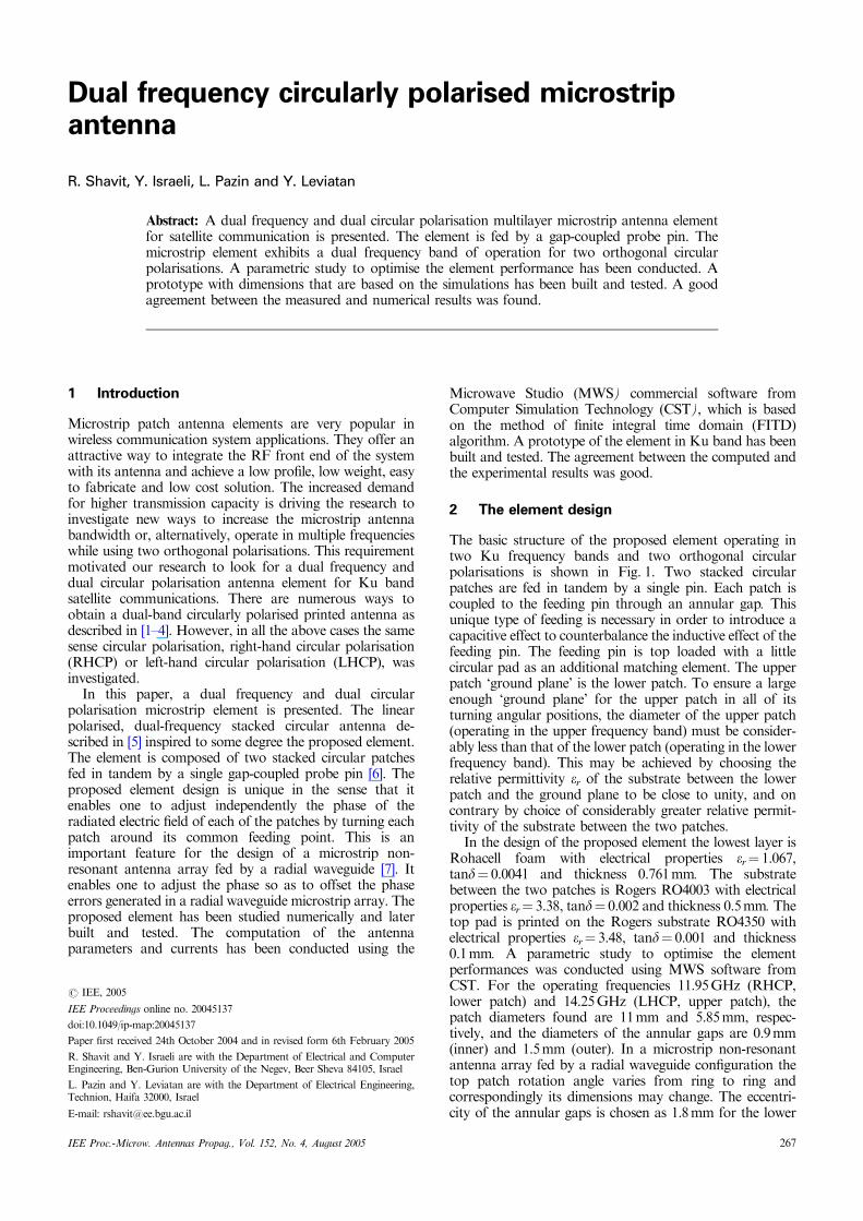
The basic structure of the proposed element operating intwo Ku frequency bands and two orthogonal circularpolarisations is shown in Fig. 1. Two stacked circularpatches are fed in tandem by a single pin. Each patch iscoupled to the feeding pin through an annular gap. Thisunique type of feeding is necessary in order to introduce acapacitive effect to counterbalance the inductive effect of thefeeding pin. The feeding pin is top loaded with a littlecircular pad as an additional matching element. The upperpatch ‘ground plane’ is the lower patch. To ensure a largeenough ‘ground plane’ for the upper patch in all of itsturning angular positions, the diameter of the upper patch(operating in the upper frequency band) must be consider-ably less than that of the lower patch (operating in the lowerfrequency band). This may be achieved by choosing therelative permittivity er of the substrate between the lowerpatch and the ground plane to be close to unity, and oncontrary by choice of considerably greater relative permit-tivity of the substrate between the two patches.
In the design of the proposed element the lowest layer isRohacell foam with electrical properties er¼ 1.067,tand¼ 0.0041 and thickness 0.761mm. The substratebetween the two patches is Rogers RO4003 with electricalproperties er¼ 3.38, tand¼ 0.002 and thickness 0.5mm. Thetop pad is printed on the Rogers substrate RO4350 withelectrical properties er¼ 3.48, tand¼ 0.001 and thickness0.1mm. A parametric study to optimise the elementperformances was conducted using MWS software fromCST. For the operating frequencies 11.95GHz (RHCP,lower patch) and 14.25GHz (LHCP, upper patch), thepatch diameters found are 11mm and 5.85mm, respec-tively, and the diameters of the annular gaps are 0.9mm(inner) and 1.5mm (outer). In a microstrip non-resonantantenna array fed by a radial waveguide configuration thetop patch rotation angle varies from ring to ring andcorrespondingly its dimensions may change. The eccentri-city of the annular gaps is chosen as 1.8mm for the lower
267
patch and 0.9mm for the upper patch, to matchthe radiation element 50ohm input impedance [8]. Thecorresponding optimum pad diameter is 1.3mm.The diameter of the feeding pin is equal to 0.3mm andthe diameter of the pin together with the soldered metalisedlayer in the substrate package is equal to 0.7mm. The entiremultilayer structure is bonded with adhesive films. Thechoice of the films has been made based on practicalconsiderations and available adhesive films with electricalproperties as close as possible to the correspondingsubstrate. The adhesive film used to bond the RO4350substrate to the RO4003 substrate is of thickness 0.1mmand electrical properties er¼ 3.17, tand¼ 0.005, while onboth sides of the foam the adhesive films used are ofthickness 0.03mm and electrical properties er¼ 5,tand¼ 0.005. The circular polarisation is achieved for eachcircular patch by introducing two indents as described in [9].The indent dimensions are 1.01� 0.52mm for the upperpatch and 1.95� 0.98mm for the lower patch.
foamlower patch
upper patchsolder top load pad
gaps
substrates adhesive films
pinground plane
a
b
Fig. 1 Geometry of the dual frequency, dual circular polarisationmicrostrip antennaa Cross-sectionb Top view
268
3 Numerical and test results
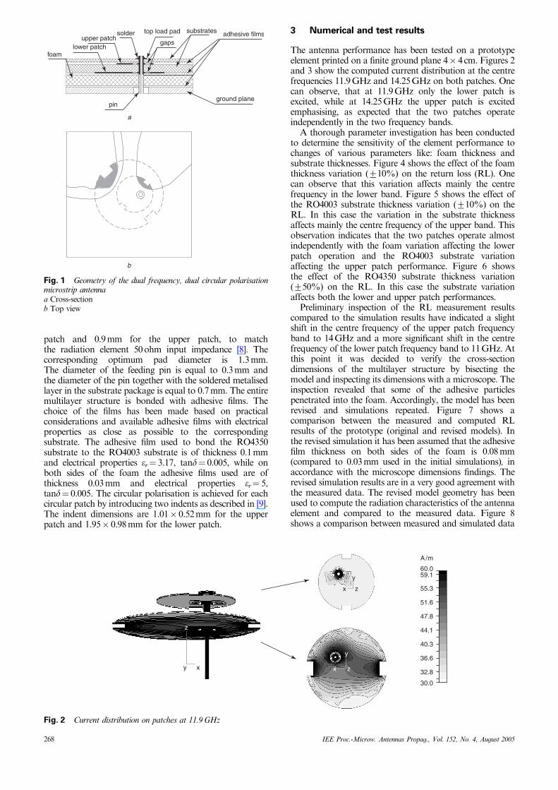
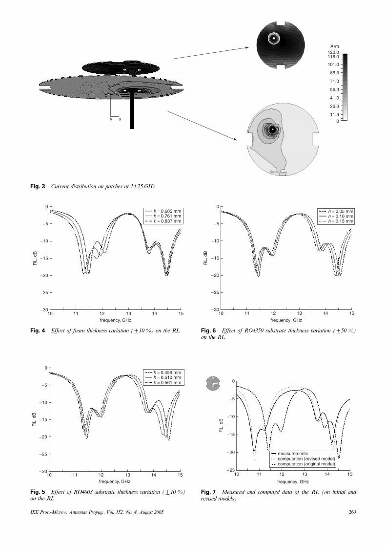
The antenna performance has been tested on a prototypeelement printed on a finite ground plane 4� 4cm. Figures 2and 3 show the computed current distribution at the centrefrequencies 11.9GHz and 14.25GHz on both patches. Onecan observe, that at 11.9GHz only the lower patch isexcited, while at 14.25GHz the upper patch is excitedemphasising, as expected that the two patches operateindependently in the two frequency bands.
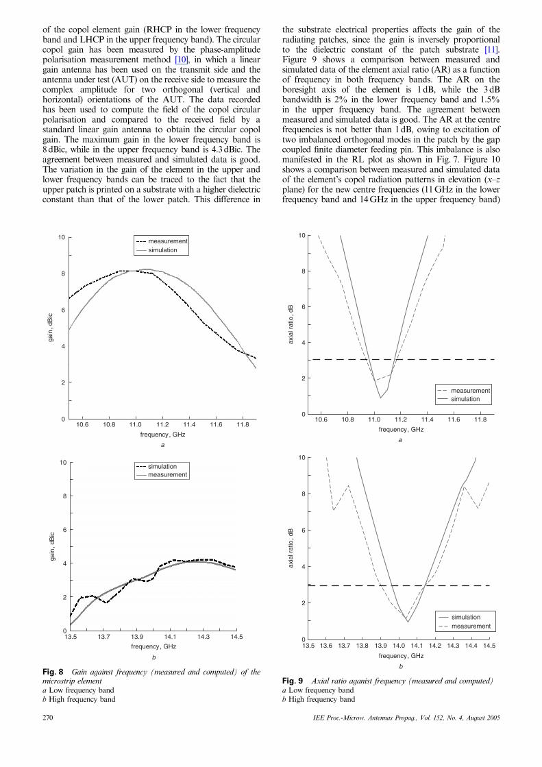
A thorough parameter investigation has been conductedto determine the sensitivity of the element performance tochanges of various parameters like: foam thickness andsubstrate thicknesses. Figure 4 shows the effect of the foamthickness variation (710%) on the return loss (RL). Onecan observe that this variation affects mainly the centrefrequency in the lower band. Figure 5 shows the effect ofthe RO4003 substrate thickness variation (710%) on theRL. In this case the variation in the substrate thicknessaffects mainly the centre frequency of the upper band. Thisobservation indicates that the two patches operate almostindependently with the foam variation affecting the lowerpatch operation and the RO4003 substrate variationaffecting the upper patch performance. Figure 6 showsthe effect of the RO4350 substrate thickness variation(750%) on the RL. In this case the substrate variationaffects both the lower and upper patch performances.
Preliminary inspection of the RL measurement resultscompared to the simulation results have indicated a slightshift in the centre frequency of the upper patch frequencyband to 14GHz and a more significant shift in the centrefrequency of the lower patch frequency band to 11GHz. Atthis point it was decided to verify the cross-sectiondimensions of the multilayer structure by bisecting themodel and inspecting its dimensions with a microscope. Theinspection revealed that some of the adhesive particlespenetrated into the foam. Accordingly, the model has beenrevised and simulations repeated. Figure 7 shows acomparison between the measured and computed RLresults of the prototype (original and revised models). Inthe revised simulation it has been assumed that the adhesivefilm thickness on both sides of the foam is 0.08mm(compared to 0.03mm used in the initial simulations), inaccordance with the microscope dimensions findings. Therevised simulation results are in a very good agreement withthe measured data. The revised model geometry has beenused to compute the radiation characteristics of the antennaelement and compared to the measured data. Figure 8shows a comparison between measured and simulated data
x z
y
x z
y
z
y x
60.059.1
55.3
51.6
47.8
44.1
40.3
36.6
32.8
30.0
A /m
Fig. 2 Current distribution on patches at 11.9 GHz
IEE Proc.-Microw. Antennas Propag., Vol. 152, No. 4, August 2005
120.0116.0
101.0
011.3
26.3
41.3
56.3
71.3
86.3
A/m
xy
z
Fig. 3 Current distribution on patches at 14.25 GHz
h = 0.685 mm
h = 0.837 mmh = 0.761 mm
0
−5
−10
−15
−20
−25
−30
RL,
dB
10 11 12 13 14 15
frequency, GHz
Fig. 4 Effect of foam thickness variation (710 %) on the RL
h = 0.459 mm
h = 0.561 mmh = 0.510 mm
0
−5
−10
−15
−20
−25
−30
RL,
dB
10 11 12 13 14 15
frequency, GHz
Fig. 5 Effect of RO4003 substrate thickness variation (710 %)on the RL
IEE Proc.-Microw. Antennas Propag., Vol. 152, No. 4, August 2005
10 11 12 13 14 15
frequency, GHz
−30
−25
−20
−15
−10
−5
0R
L, d
Bh = 0.05 mmh = 0.10 mmh = 0.15 mm
Fig. 6 Effect of RO4350 substrate thickness variation (750 %)on the RL
measurementscomputation (revised model)computation (original model)
10 11 12 13 14 15
frequency, GHz
−25
−20
−15
−10
−5
0
RL,
dB
y
z x
Fig. 7 Measured and computed data of the RL (on initial andrevised models)
269
of the copol element gain (RHCP in the lower frequencyband and LHCP in the upper frequency band). The circularcopol gain has been measured by the phase-amplitudepolarisation measurement method [10], in which a lineargain antenna has been used on the transmit side and theantenna under test (AUT) on the receive side to measure thecomplex amplitude for two orthogonal (vertical andhorizontal) orientations of the AUT. The data recordedhas been used to compute the field of the copol circularpolarisation and compared to the received field by astandard linear gain antenna to obtain the circular copolgain. The maximum gain in the lower frequency band is8dBic, while in the upper frequency band is 4.3dBic. Theagreement between measured and simulated data is good.The variation in the gain of the element in the upper andlower frequency bands can be traced to the fact that theupper patch is printed on a substrate with a higher dielectricconstant than that of the lower patch. This difference in
10.6 10.8 11.0 11.2 11.4 11.6 11.8
frequency, GHz
0
2
4
6
8
10
gain
, dB
ic
measurementsimulation
a
13.5 13.7 13.9 14.1 14.3 14.5
frequency, GHz
0
2
4
6
8
10
gain
, dB
ic
measurementsimulation
b
Fig. 8 Gain against frequency (measured and computed) of themicrostrip elementa Low frequency bandb High frequency band
270
the substrate electrical properties affects the gain of theradiating patches, since the gain is inversely proportionalto the dielectric constant of the patch substrate [11].Figure 9 shows a comparison between measured andsimulated data of the element axial ratio (AR) as a functionof frequency in both frequency bands. The AR on theboresight axis of the element is 1dB, while the 3dBbandwidth is 2% in the lower frequency band and 1.5%in the upper frequency band. The agreement betweenmeasured and simulated data is good. The AR at the centrefrequencies is not better than 1dB, owing to excitation oftwo imbalanced orthogonal modes in the patch by the gapcoupled finite diameter feeding pin. This imbalance is alsomanifested in the RL plot as shown in Fig. 7. Figure 10shows a comparison between measured and simulated dataof the element’s copol radiation patterns in elevation (x–zplane) for the new centre frequencies (11GHz in the lowerfrequency band and 14GHz in the upper frequency band)
10.6 10.8 11.0 11.2 11.4 11.6 11.8
frequency, GHz
0
2
4
6
8
10
axia
l rat
io, d
B
measurementsimulation
a
13.5 13.6 13.7 13.913.8 14.114.0 14.314.2 14.4 14.5
frequency, GHz
0
2
4
6
8
10
axia
l rat
io, d
B
simulationmeasurement
b
Fig. 9 Axial ratio aganist frequency (measured and computed)a Low frequency bandb High frequency band
IEE Proc.-Microw. Antennas Propag., Vol. 152, No. 4, August 2005
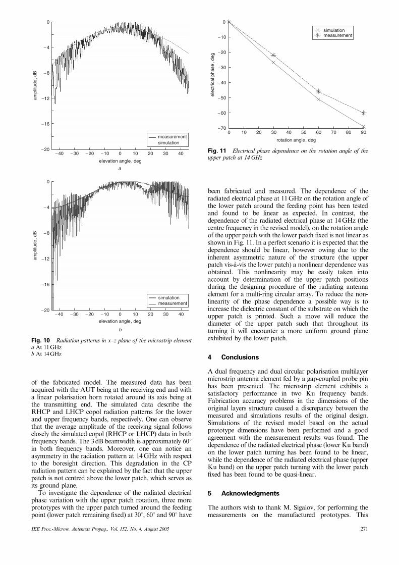
of the fabricated model. The measured data has beenacquired with the AUT being at the receiving end and witha linear polarisation horn rotated around its axis being atthe transmitting end. The simulated data describe theRHCP and LHCP copol radiation patterns for the lowerand upper frequency bands, respectively. One can observethat the average amplitude of the receiving signal followsclosely the simulated copol (RHCP or LHCP) data in bothfrequency bands. The 3dB beamwidth is approximately 601in both frequency bands. Moreover, one can notice anasymmetry in the radiation pattern at 14GHz with respectto the boresight direction. This degradation in the CPradiation pattern can be explained by the fact that the upperpatch is not centred above the lower patch, which serves asits ground plane.
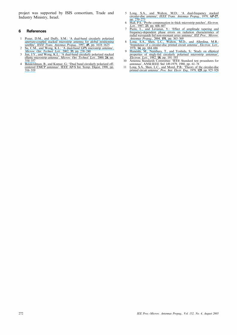
To investigate the dependence of the radiated electricalphase variation with the upper patch rotation, three moreprototypes with the upper patch turned around the feedingpoint (lower patch remaining fixed) at 301, 601 and 901 have
−40 −30 −20 −10 0 10 20 30 40−20
−16
−12
−8
−4
0
elevation angle, deg
simulationmeasurement
ampl
itude
, dB
−40 −30 −20 −10 0 10 20 30 40−20
−16
−12
−8
−4
0
elevation angle, deg
simulationmeasurement
ampl
itude
, dB
a
b
Fig. 10 Radiation patterns in x–z plane of the microstrip elementa At 11GHzb At 14GHz
IEE Proc.-Microw. Antennas Propag., Vol. 152, No. 4, August 2005
been fabricated and measured. The dependence of theradiated electrical phase at 11GHz on the rotation angle ofthe lower patch around the feeding point has been testedand found to be linear as expected. In contrast, thedependence of the radiated electrical phase at 14GHz (thecentre frequency in the revised model), on the rotation angleof the upper patch with the lower patch fixed is not linear asshown in Fig. 11. In a perfect scenario it is expected that thedependence should be linear, however owing due to theinherent asymmetric nature of the structure (the upperpatch vis-"a-vis the lower patch) a nonlinear dependence wasobtained. This nonlinearity may be easily taken intoaccount by determination of the upper patch positionsduring the designing procedure of the radiating antennaelement for a multi-ring circular array. To reduce the non-linearity of the phase dependence a possible way is toincrease the dielectric constant of the substrate on which theupper patch is printed. Such a move will reduce thediameter of the upper patch such that throughout itsturning it will encounter a more uniform ground planeexhibited by the lower patch.
4 Conclusions
A dual frequency and dual circular polarisation multilayermicrostrip antenna element fed by a gap-coupled probe pinhas been presented. The microstrip element exhibits asatisfactory performance in two Ku frequency bands.Fabrication accuracy problems in the dimensions of theoriginal layers structure caused a discrepancy between themeasured and simulations results of the original design.Simulations of the revised model based on the actualprototype dimensions have been performed and a goodagreement with the measurement results was found. Thedependence of the radiated electrical phase (lower Ku band)on the lower patch turning has been found to be linear,while the dependence of the radiated electrical phase (upperKu band) on the upper patch turning with the lower patchfixed has been found to be quasi-linear.
5 Acknowledgments
The authors wish to thank M. Sigalov, for performing themeasurements on the manufactured prototypes. This
0 10 20 30 40 50 60 70 80 90
rotation angle, deg
−70
−60
−50
− 40
−30
−20
−10
0
elec
tric
al p
hase
, deg
measurementsimulation
Fig. 11 Electrical phase dependence on the rotation angle of theupper patch at 14 GHz
271
project was supported by ISIS consortium, Trade andIndustry Ministry, Israel.
6 References
1 Pozar, D.M., and Duffy, S.M.: ‘A dual-band circularly polarizedaperture-coupled stacked microstrip antenna for global positioningsatellite’, IEEE Trans. Antennas Propag., 1997, 45, pp. 1618–1625
2 Su, C.M., and Wong, K.L.: ‘A dual-band GPS microstrip antenna’,Microw. Opt. Technol. Lett., 2002, 33, pp. 238–240
3 Jan, J.Y., and Wong, K.L.: ‘A dual-band circularly polarized stackedelliptic microstrip antenna’, Microw. Opt. Technol. Lett., 2000, 24, pp.354–357
4 Balakrishnan, B., and Kumar, G.: ‘Dual band circularly polarized off-centered EMCP antennas’. IEEE AP-S Int. Symp. Digest, 1998, pp.316–319
272
5 Long, S.A., and Walton, M.D.: ‘A dual-frequency stackedcircular-disc antenna’, IEEE Trans. Antennas Propag., 1979, AP-27,pp. 270–273
6 Hall, P.S.: ‘Probe compensation in thick microstrip patches’, Electron.Lett., 1987, 23, pp. 606–607
7 Pazin, L., and Leviatan, Y.: ‘Effect of amplitude tapering andfrequency-dependent phase errors on radiation characteristics ofradial waveguide fed non-resonant array antenna’, IEE Proc., Microw.Antennas Propag., 2004, 151, pp. 363–369
8 Long, S.A., Shen, L.C., Walton, M.D., and Allerding, M.R.:‘Impedance of a circular-disc printed circuit antenna’, Electron. Lett.,1978, 14, pp. 684–686
9 Haneishi, M., Nambara, T., and Yoshida, S.: ‘Study on ellipticalproperties of singly-fed circularly polarised microstrip antennas’,Electron. Lett., 1982, 18, pp. 191–193
10 Antenna Standards Committee: ‘IEEE Standard test procedures forantennas’, ANSI/IEEE Std 149-1979, 1980, pp. 61–78
11 Long, S.A., Shen, L.C., and Morel, P.B.: ‘Theory of the circular-discprinted circuit antenna’, Proc. Inst. Electr. Eng., 1978, 125, pp. 925–928
IEE Proc.-Microw. Antennas Propag., Vol. 152, No. 4, August 2005


