Embed Size (px)
Citation preview
PHYSICAL REVIEW B 67, 245108 ~2003!
Electronic and optical properties of Y2SiO5 and Y2Si2O7 with comparisons to a-SiO2 and Y2O3
W. Y. Ching,* Lizhi Ouyang, and Yong-Nian XuDepartment of Physics, University of Missouri-Kansas City, Kansas City, Missouri 64110, U.S.A.
~Received 25 February 2003; published 23 June 2003!
The electronic structure and bonding in two complex crystals, yttrium oxyorthosilicate Y2SiO5 and yttriumpyrosilicate Y2Si2O7 , were studied by means of first-principles local density calculations. Both crystals areionic insulators with large band gaps. It is shown that their electronic structure and bonding cannot be repre-sented by the weighted sums of those ofa-SiO2 and Y2O3 . On average, the Si-O~Y-O! bond in the ternarycrystals tends to be weaker~stronger! than the respective bond ina-SiO2(Y2O3). It is further shown that thespecific local atomic coordinations can lead to significantly different partial density of states that should beexperimentally detectable. The bulk and optical properties of these two crystals were also calculated. We findthe bulk modulus of Y2SiO5(Y2Si2O7) to be 134.8 GPa~140.2 GPa!. The optical dielectric constants for thetwo crystals are estimated to be 3.11 and 3.44, respectively. In the absence of any experimental data, thesevalues are presented as theoretical predictions.
DOI: 10.1103/PhysRevB.67.245108 PACS number~s!: 71.20.Ps
ryo
e.tu
p
so
notwlaysur
erputhuche
heth
eof-it,
tin
p
taled
tals
be
ted
he
heare
n
-ng.
dis
nicte
lec-ofr
canen-no-d aseofd
I. INTRODUCTION
SiO2 and Y2O3 are some of the most important binaoxides and are also fundamental ingredients of other mcomplex oxides. SiO2 has many polymorphs witha-SiO2
~quartz!, the most well-known stable phase.1 In contrast,Y2O3 has only one known phase with a bixbyte structur2
Many research groups have studied the electronic strucand bonding in crystalline SiO2 in the past.1,3–7 Within thelast decade, there has also been considerable attentionto the electronic and optical properties of the Y2O3
crystal.8–11 Between the SiO2 and Y2O3 phase boundariethere are two well-established yttrium silicates, Y-oxyorthsilicate or Y2SiO5(SiO21Y2O3) and Y-pyrosilicate orY2Si2O7(2 SiO21Y2O3). Conspicuously, there has beenstudy on the electronic structure and bonding of theseternary crystals. There could be several reasons for theof such efforts. First, the crystal structures of these two crtals are much more complicated and their precise structhave not been determined until very recently.12 Second, be-cause of the complexity of these crystal structures, fullabinitio electronic structure calculations still require considable effort even in this era of rapid advancement in comtational methods and techniques. Third, it is conceivablethere could be nothing spectacular in their electronic strture and bonding. Most likely, their properties are just tweighted averages of the two end members SiO2 and Y2O3.
Y2SiO5 is an important laser crystal that has been syntsized since 1961.13 Most research activities connected wiY2SiO5 have been related to rare-earth (Ce31, Eu31, etc.!doped crystals to be used as blue phosphor14,15 or inCr41-doped Y2SiO5 to be applied as a saturable-absorbQ-switch laser.16 This is mainly because the substitutionSi41 in Y2SiO5 by a Cr41 ion entails no other chargecompensating ions and has the highest figure of mer16
whereas in systems such as Cr41 in Y3Al5O12 ~YAG!, itrequires the addition of Ca or Mg as charge-compensaions, which could affect the laser operation.20 Although thereare many reports on the spectroscopic studies of do
0163-1829/2003/67~24!/245108~8!/$20.00 67 2451
re
re
aid
-
ock-
es
--
at-
-
r
g
ed
Y2SiO5 , we are not aware of any studies of the fundamenproperties of the host crystal itself. We have recently arguthat for a proper understanding of laser operations in cryssuch as Y3Al5O12, YAlO3 , BeAl2O4 , or LiYF4 ,17–20 theelectronic structure and bonding of the host crystal mustunderstood first. On the other hand, study of Y2Si2O7 ismuch less common. It is mostly recognized as a precipitaphase in the interlayers joining Si3N4 ceramics with Si2N2Oor SiO2 glass21 and is considered to be a critical phase in tSiO2-Y2O3-Si3N4 phase diagram.22,23 Within the complexphase diagram of SiO2-Y2O3-Si3N4 , there are a total of tenidentified crystalline phases, three at the corners (SiO2 ,Y2O3, and Si3N4), three on the edges (Si2N2O betweenSiO2 and Si3N4 , Y2SiO5 , and Y2Si2O7 between SiO2 andY2O3), and four in the interior of the phase diagram. Tquaternary crystals at the interior of the phase diagramY10@SiO4#6N2 ~N-apatite!, Y2Si3N4O3 ~M-melilite!,Y4Si2O7N2 , ~J-phase or N-YAM!, and YSiO2N ~N-wallastonite!. Y2Si2O7 is at the corner of what has beecalled the compatibility triangle~with corners at Si2N2O,Si3N4 and Y2Si2O7), which may play some role in the formation of different phases during high-temperature sinteriThere are claims that other polymorphs of Y2SiO5 andY2Si2O7 could exist,24 but to our knowledge, no detaileinformation on their structures has been published. Ithighly desirable to initiate a detailed study on the electrostructure and bonding in the two complex yttrium silicacrystals.
In this paper, we present a detailed calculation of the etronic structure and bonding, bulk, and optical propertiesY2SiO5 and Y2Si2O7 crystals and compare them with similacalculations ona-SiO2 and Y2O3.25 We are mostly con-cerned with the subtle differences in those properties thatbe attributed to their specific crystal structure and localvironment. Our calculations demonstrate that the naivetion that the properties of Y-Si-O systems can be describethe average of SiO2 and Y2O3 is grossly inadequate. In thfollowing section, we will describe the crystal structuresY2SiO5 and Y2Si2O7 . The method of calculation is outline
©2003 The American Physical Society08-1
W. Y. CHING, LIZHI OUYANG, AND YONG-NIAN XU PHYSICAL REVIEW B 67, 245108 ~2003!
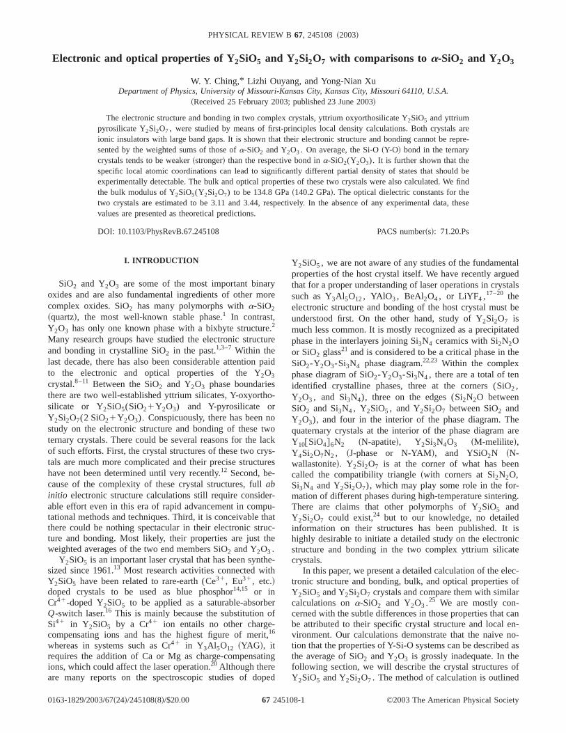
FIG. 1. Crystal structure ofY2SiO5 and Y2Si2O7 .
tediga
leyu
eumnt
ith
dto
m’s
m
ile
ur0ly7
or
d
7
on-
n
edon.rlyhehedeasis
ofn-ets
al
gy
nal
aln-
in
in Sec. III. The main results of the calculation are presenand discussed in Sec. IV. In the last section, some concluremarks and a comment on the direction of future investitions are made.
II. CRYSTAL STRUCTURE
The crystal structures of Y2Si2O7 and Y2SiO5 aresketched in Fig. 1. The lattice constants are listed in TabWe used the crystal data recently reported by Leonet al.12 The single-crystal sample for Y2SiO5 is Cr dopedwhile that of Y2Si2O7 is undoped. They were grown by thCzochralski technique in a high-frequency heated iridicrucible. The crystal parameters determined are significadifferent from the ones reported more than 30 years ago.26,27
The crystal structures of Y2SiO5 and Y2Si2O7 are fairlycomplicated. They both have a monoclinic lattice but wdifferent space groups,B2/b for Y2SiO5 and P21 /c forY2Si2O7 . In Y2SiO5 , the unit cell contains 32 atoms (Z54) with two different Y sites Y1 and Y2, one Si site, anfive O sites, which we will label as O1–O5. Y1 bondsseven O ions with bond lengths~BL! ranging from 2.199 Åto 2.604 Å. Y2 bonds to only six O ions with ranging fro2.203 Å to 2.287 Å. Si is tetrahedrally bonded to four Owith two short bonds (BL51.602 Å and 1.605 Å! and twolonger bonds (BL51.628 Å and 1.636 Å!. O1 is the only Oatom in Y2SiO5 that has no Si as a nearest neighbor~NN!and is loosely bonded to four Y ions with BL’s ranging fro
TABLE I. Crystal parameters and interatomic distancesY2SiO5 and Y2Si2O7 from Ref. 5.
Crystals Y2SiO5 Y2Si2O7
Space group C2/c P21 /cLattice constantsa ~Å! 14.371 4.694b ~Å! 6.71 10.856c ~Å! 10.388 5.588b 122.17° 95.01°Cation coordination Y1-O7, Y2-O6 Y-O6
SiO4 Si-O4
24510
dng-
I.k
ly
2.199 Å to 2.373 Å. O2 bonds to three Y and one Si whO3, O4, and O5 all bond to one Si and two Y.
In Y2Si2O7 , there is only one Y site, one Si site, and foO sites. Y has six NN O ions with BL’s ranging from 2.25Å to 2.328 Å. Si is at the tetrahedral site with BL’s slightdifferent from that in Y2SiO5 ~1.616, 1.622, 1.631, and 1.63Å!. O1 is the only atom in a bridging position with two NNSi. O2, O3, and O4 all have two Y and one Si as NN’s. Fcomparison, we recall that ina-SiO2 , O is in a bridgingposition while Si is tetrahedrally bonded with Si-O bonlengths of 1.605 Å and 1.614 Å. In Y2O3, both Y1(8a) andY2(24d) bond to six O atoms with BL’s of 2.244 Å, 2.33Å, and 2.268 Å. There is only one unique O (48e) site whichbonds to four Y atoms similar to O1 in Y2SiO5 . We willfurther discuss the implications of these local structural cfigurations on the calculated electron density of states~DOS!in these two crystals in Sec. IV.
III. METHOD OF CALCULATION
We used theab initio orthogonalized linear combinatioof atomic orbitals ~OLCAO! method28 for the electronicstructure calculation. In the OLCAO method, the localizatomic basis is used in the expansion of the Bloch functiThis localized description of the orbital basis is particulaeffective in describing the bonding in complex crystals. Tmethod has been well described in many recently publispapers.17–20,29–35Here, we briefly outline the details that arpertinent to the present calculation. In both crystals, the bsets consist of Y1s, 2s, 3s, 4s, 5s, 6s, 2p, 3p, 4p, 5p,3d, 4d, 5d; Si 1s, 2s, 3s, 4s, 2p, 3p, 4p, 3d, O 1s, 2s,3s, 2p, 3p atomic orbitals, which are expanded in termsa Gaussian-type of orbital~GTO!. These basis sets are geerally referred to as full basis sets. The minimal basis swill have Y 6s, Y 5d, Si 4s, 4p, 3d and O 3s, 3p removedfrom the full basis sets. The core orbitals~those underlined!were orthogonalized to the ‘‘non core’’ orbitals in the usu‘‘frozen-core’’ approximation. The semi core Y 4p orbitalwas treated as a ‘‘none-core’’ orbital since its orbital eneris only slightly lower than that of O 2s. The crystal poten-tials were constructed according to the density functiotheory with the local approximation~DFT-LDA!.36 Wigner-interpolation formula was employed to account for additioncorrelation effects in the LDA potential. The crystal pote
8-2
n
onuio
uluienvere
ati-lasi
m
h
tharu
-th
thetnie
otly,f
be
-
ndno
ee-t
of
ELECTRONIC AND OPTICAL PROPERTIES OF Y2SiO5 . . . PHYSICAL REVIEW B67, 245108 ~2003!
tials were expanded in terms of atom-centered analytic futions consisting of a combination ofs-type Guassians. Weused the experimental lattice parameters for the electrstructure and optical properties studies. In the case of grostate bulk properties, we used a total-energy minimizatscheme for geometry optimization.37,38 Geometry optimiza-tion is necessary in order to obtain an accurate bulk modin which all crystal parameters are simultaneously varwhen the crystal volume is compressed or dilated. The boing properties are described in terms of Mulliken effectiatomic charge and bond order values between neaneighbor pairs. For these calculations, separate minimbasis sets were used to obtain a more meaningful descripsince the Mulliken scheme39 works best when the basis functions are more localized. For the optical properties calcution, the dipole transition matrices were included for trantions from the occupied valence band~VB! ~including thoseof Y 4p) to the unoccupied conduction band~CB!. To im-prove the accuracy of higher CB states, additional atoobitals ~Y 7s, 6p, 6d, Si 5s, 5p, 4d, and O 4s, 4p) wereadded to the basis set in the optical calculation, whichgenerally referred to as an extended basis set. Even witextended basis set, the optical calculations were limitedtransitions no higher than 35 eV since the accuracy ofwave functions of the high CB states cannot be fully guanteed in a method based on the variational principle. A sficiently large number ofk points in the irreducible portionof the Brillouin zones~BZ! were used~64 and 54 for Y2SiO5and Y2Si2O7 , respectively! both in the self-consistent iterations and in the final analysis of the DOS as well as inoptical properties calculations.
IV. RESULTS
A. Band structure and density of states
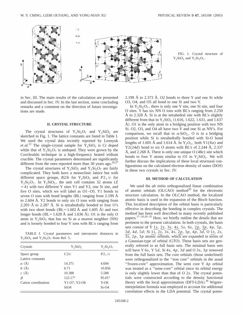
The band structures and the DOS of Y2SiO5 and Y2Si2O7were calculated using the OLCAO method. Fig. 2 showsband structures of the two crystals along the high-symmlines of the BZ. These band structures are typical of ioinsulators with relatively large band gaps and flat-toppVB’s. The gaps are direct, 4.82 eV for Y2SiO5 and 4.78 eVfor Y2Si2O7 . The real gaps may be somewhat larger in bcrystals since it is well known that LDA theory generalunderestimates the band gaps of insulators. In both casesbottom of the CB is atG and consists of a single band opredominately Y 4d and Si 4s character. The top of the VB
FIG. 2. Calculated band structure of Y2SiO5 and Y2Si2O7 .
24510
c-
icndn
sdd-
st-l-on
--
ic
isantoe-f-
e
erycd
h
the
may not be exactly at theG point but the difference is sosmall that the gaps in both crystals can be considered todirect band gaps.
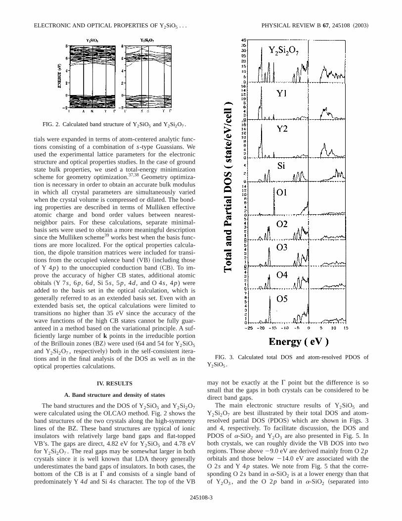
The main electronic structure results of Y2SiO5 andY2Si2O7 are best illustrated by their total DOS and atomresolved partial DOS~PDOS! which are shown in Figs. 3and 4, respectively. To facilitate discussion, the DOS aPDOS ofa-SiO2 and Y2O3 are also presented in Fig. 5. Iboth crystals, we can roughly divide the VB DOS into twregions. Those above29.0 eV are derived mainly from O 2porbitals and those below214.0 eV are associated with thO 2s and Y 4p states. We note from Fig. 5 that the corrsponding O 2s band ina-SiO2 is at a lower energy than thaof Y2O3, and the O 2p band in a-SiO2 ~separated into
FIG. 3. Calculated total DOS and atom-resolved PDOSY2SiO5 .
8-3
ae
otet
y5r-Nh
hetioa
yY1
ts
s
gnt
aveec.
O’sle
ctshox-ely,
Btry
o
W. Y. CHING, LIZHI OUYANG, AND YONG-NIAN XU PHYSICAL REVIEW B 67, 245108 ~2003!
two segments! is much wider than the O 2p bands in Y2O3.Focusing on Y2SiO5 , we can summarize our observationsfollows: ~1! The PDOS of O1 is totally different from thPDOS of the other four oxygens. It has a sharp O 2s peak at215.1 eV and a narrow O 2p band. This is because O1 is nbonded to any Si atom but to four Y ions with much longY-O bonds. The PDOS profile has a great resemblance toO PDOS of Y2O3. This indicates that Y-O is a relativelweak bond in Y2SiO5 . ~2! The PDOS of O2, O3, O4, and Oare all very similar. As discussed in Sec. II, the only diffeence among them is that O2 has three Y and one Si aswhereas O3, O4, and O5 have two Y and one Si as NN. Tsmall difference is reflected in the slight difference in tPDOS near the top of the VB. This reenforces the asserthat Y-O is a relatively weak bond and its main influence isthe top of the VB.~3! The PDOS for Y1 and Y2 are versimilar. Their only difference is in the CB PDOS becausehas an extra O as NN atom.~4! The PDOS of Si, which istetrahedrally coordinated, resembles to some extentPDOS in a-SiO2 . Both the upper and the lower sectionbreak into multiple segments.
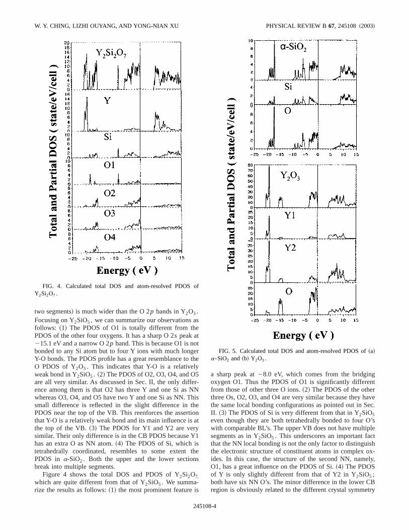
Figure 4 shows the total DOS and PDOS of Y2Si2O7,which are quite different from that of Y2SiO5 . We summa-rize the results as follows:~1! the most prominent feature i
FIG. 4. Calculated total DOS and atom-resolved PDOSY2Si2O7 .
24510
s
rhe
Nis
nt
he
a sharp peak at28.0 eV, which comes from the bridginoxygen O1. Thus the PDOS of O1 is significantly differefrom those of other three O ions.~2! The PDOS of the otherthree Os, O2, O3, and O4 are very similar because they hthe same local bonding configurations as pointed out in SII. ~3! The PDOS of Si is very different from that in Y2SiO5even though they are both tetrahedrally bonded to fourwith comparable BL’s. The upper VB does not have multipsegments as in Y2SiO5 . This underscores an important fathat the NN local bonding is not the only factor to distinguithe electronic structure of constituent atoms in complexides. In this case, the structure of the second NN, namO1, has a great influence on the PDOS of Si.~4! The PDOSof Y is only slightly different from that of Y2 in Y2SiO5 ;both have six NN O’s. The minor difference in the lower Cregion is obviously related to the different crystal symme
f
FIG. 5. Calculated total DOS and atom-resolved PDOS of~a!a-SiO2 and ~b! Y2O3 .
8-4
ele
inga
sa
at ao
alin,
r
enaremal
estalande O
o
.01
e
or-heO
.c-
ghdoglef a
given bond. In Y2Si2O7 crystal, the variations of Y-O BO
ELECTRONIC AND OPTICAL PROPERTIES OF Y2SiO5 . . . PHYSICAL REVIEW B67, 245108 ~2003!
and slightly different Y-O BL’s. It is clear from the abovcalculated DOS and PDOS of the two crystals that the etronic structures of Y2SiO5 and Y2Si2O7 cannot be simplyviewed as a superposition of those of SiO2 and Y2O3 in Fig.5. The sharp peaks at215.1 eV in Y2SiO5 and28.0 eV inY2Si2O7 should be easily detected experimentally ustechniques such as x-ray photoelectron spectroscopyresonant x-ray emission spectroscopy.
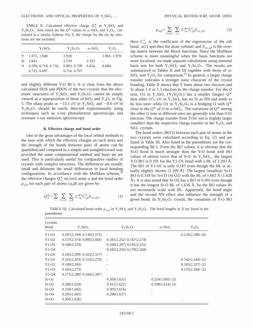
B. Effective charge and bond order
One of the great advantages of the local orbital methodthe ease with which the effective charges on each atomthe strength of the bonds between pairs of atoms canquantified and compared in a simple and straightforward wprovided the same computational method and basis seused. This is particularly useful for comparative studiescrystals with complex structures. The differences are ususmall and delineate the small differences in local bondconfigurations. In accordance with the Mulliken scheme39
the effective chargesQa* on each atoma and the bond orderab for each pair of atoms~a,b! are given by
Qa* 5(i
(n,occ
(j ,b
Cia*nCj b
n Sia, j b , ~1!
TABLE II. Calculated effective chargeQa* in Y2SiO5 andY2Si2O7 . Also listed are theQ* values ina-SiO2 and Y2O3 , cal-culated in a similar fashion. For Y, the charge for the six 4p elec-trons are not included.
Y2SiO5 Y2Si2O7 a-SiO2 Y2O3
Y 1.972, 1.940 1.928 - 1.961, 1.978Si 2.641 2.539 2.333 -O 6.599, 6.714, 6.716, 6.803, 6.709 6.834 6.684
6.721, 6.697 6.716, 6.707
24510
c-
nd
isndbeyreflyg
rab5 (n,occ
(i , j
Cia*nCj b
n Sia, j b . ~2!
Here Cian is the coefficient of the eigenvector of thenth
band.a( i ) specifies the atom~orbital! andSia, j b is the over-lap matrix between the Bloch functions. Since the Mullikscheme is more meaningful when the basis functionsmore localized, we made separate calculations using minibasis sets for both Y2SiO5 and Y2Si2O7 . The results aresummarized in Tables II and III together with those ofa-SiO2 and Y2O3 for comparison.25 In general, a larger chargtransfer indicates a stronger ionic character of the crybonding. Table II shows that Y loses about one electronSi about 1.4 or 1.5 electron in the charge transfer. For thions, O1 in Y2SiO5 (Y2Si2O7) has a smaller~larger! Q*than other O’s. O1 in Y2SiO5 has no Si as NN and tends tbe less ionic while O1 in Y2Si2O7 is a bridging O withQ*close to theQ* of O in a-SiO2 . The variations ofQ* amongthe other O ions at different sites are generally less than 0electron. The charge transfer from Y~Si! ion is slightly larger~smaller! than the respective charge transfer in the Y2O3 andSiO2 crystals.
The bond orders~BO’s! between each pair of atoms in thtwo crystals were calculated according to Eq.~2! and arelisted in Table III. Also listed in the parentheses are the cresponding BL’s. From the BO values, it is obvious that tSi-O bond is much stronger than the Y-O bond with Bvalues of almost twice that of Y-O. In Y2SiO5 , the largestY-O BO is 0.191 for the Y2-O1 bond with a BL of 2.203 ÅThe BO of Y1-O1 is only 0.187 even though the BL is atually slightly shorter~2.199 Å!. The largest~smallest! Si-OBO is 0.318 for Si-O3~Si-O2! with the BL of 1.602 Å~1.628Å!. It is also noted that Si-O5 has a BO of 0.305 even thouit has the longest Si-O BL of 1.636 Å. So the BO valuesnot necessarily scale with BL. Apparently, the bond anand the second NN effect also influence the strength o
e
TABLE III. Calculated bond orderra,b in Y2SiO5 and Y2Si2O7 . The bond lengths in Å are listed in thparentheses.CrystalsBond Y2SiO5 Y2Si2O7 a-SiO2 Y2O3
Y1-O1 0.187~2.199! 0.130~2.373! - 0.124~2.288! ~6!
Y1-O2 0.137~2.374! 0.085~2.604! 0.181~2.252! 0.167~2.274!Y1-O3 0.168~2.319! 0.160~2.297! 0.191~2.251!Y1-O4 - 0.185~2.250! 0.178~2.328!Y1-O5 0.165~2.299! 0.165~2.317! -Y2-O1 0.191~2.203! 0.153~2.279! - 0.142~2.244! ~2!
Y2-O2 0.149~2.283! - 0.105~2.337! ~2!
Y2-O3 0.183~2.275! - 0.133~2.268! ~2!
Y2-O4 0.171~2.280! 0.160~2.287! -Si-O1 - 0.309~1.631! 0.324~1.605! ~2!
Si-O2 0.286~1.628! 0.311~1.622! 0.299~1.614! ~2!
Si-O3 0.318~1.602! 0.305~1.616! -Si-O4 0.295~1.605! 0.290~1.637! -Si-O5 0.305~1.636! -
8-5
of
thfrsnforo
enticle
otheillT
trintw
hey
iserialor-rast,e
refor
ix
sed.
n-the
V. Itith
o
,
W. Y. CHING, LIZHI OUYANG, AND YONG-NIAN XU PHYSICAL REVIEW B 67, 245108 ~2003!
and BL are less than those in Y2SiO5 . The maximum BO is0.185 for Y-O4 ~BL52.250 Å! and the minimum BO is0.160 for Y-O3~BL52.297 Å!. Likewise, the Si-O BO andBL values in Y2Si2O7 fall between the limits for the Y2SiO5crystal. Again, the largest Si-O BO of 0.311 for Si-O2~BL51.622 Å! is larger than that of the Si-O4 pair~BO50.306!with a shorter BL of 1.616 Å. Comparing the BO valuesthe binary crystalsa-SiO2 and Y2O3, we find the BO forSi-O bonds in Y2SiO5 and Y2Si2O7 are slightly weaker thanthose ina-SiO2 , while the BO of Y-O bonds are slightlylarger than those in Y2O3.
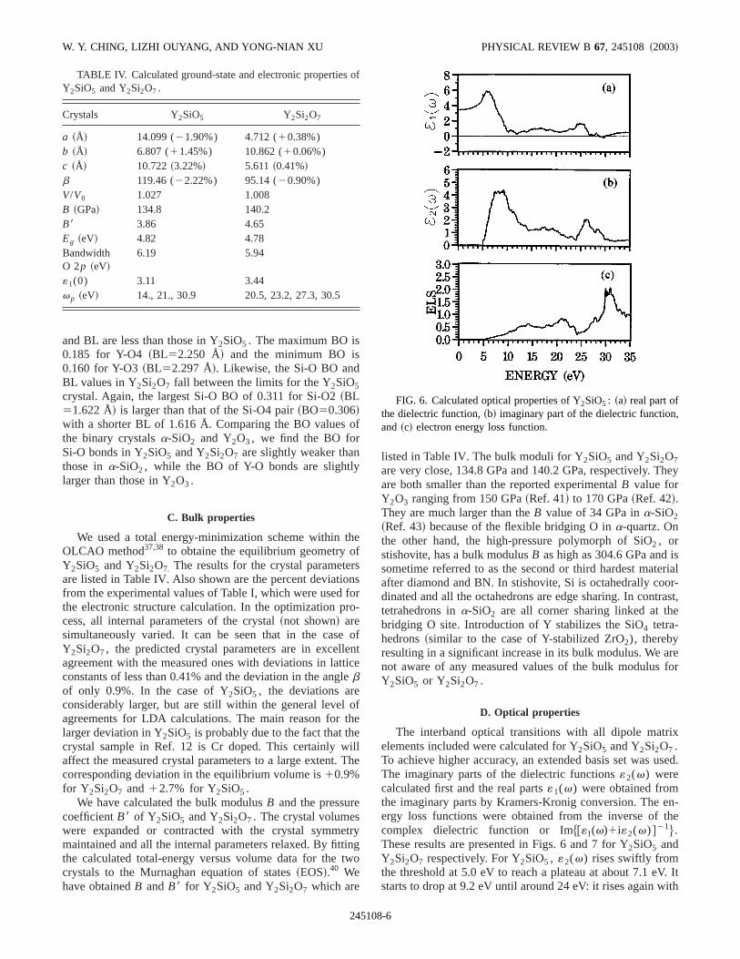
C. Bulk properties
We used a total energy-minimization scheme withinOLCAO method37,38 to obtaine the equilibrium geometry oY2SiO5 and Y2Si2O7. The results for the crystal parameteare listed in Table IV. Also shown are the percent deviatiofrom the experimental values of Table I, which were usedthe electronic structure calculation. In the optimization pcess, all internal parameters of the crystal~not shown! aresimultaneously varied. It can be seen that in the caseY2Si2O7 , the predicted crystal parameters are in excellagreement with the measured ones with deviations in latconstants of less than 0.41% and the deviation in the angbof only 0.9%. In the case of Y2SiO5 , the deviations areconsiderably larger, but are still within the general levelagreements for LDA calculations. The main reason forlarger deviation in Y2SiO5 is probably due to the fact that thcrystal sample in Ref. 12 is Cr doped. This certainly waffect the measured crystal parameters to a large extent.corresponding deviation in the equilibrium volume is10.9%for Y2Si2O7 and12.7% for Y2SiO5 .
We have calculated the bulk modulusB and the pressurecoefficientB8 of Y2SiO5 and Y2Si2O7 . The crystal volumeswere expanded or contracted with the crystal symmemaintained and all the internal parameters relaxed. By fittthe calculated total-energy versus volume data for thecrystals to the Murnaghan equation of states~EOS!.40 Wehave obtainedB andB8 for Y2SiO5 and Y2Si2O7 which are
TABLE IV. Calculated ground-state and electronic propertiesY2SiO5 and Y2Si2O7 .
Crystals Y2SiO5 Y2Si2O7
a ~Å! 14.099 (21.90%) 4.712 (10.38%)b ~Å! 6.807 (11.45%) 10.862 (10.06%)c ~Å! 10.722~3.22%! 5.611~0.41%!
b 119.46 (22.22%) 95.14 (20.90%)V/V0 1.027 1.008B ~GPa! 134.8 140.2B8 3.86 4.65Eg ~eV! 4.82 4.78BandwidthO 2p ~eV!
6.19 5.94
«1(0) 3.11 3.44vp ~eV! 14., 21., 30.9 20.5, 23.2, 27.3, 30.5
24510
e
sr-
ofte
fe
he
ygo
listed in Table IV. The bulk moduli for Y2SiO5 and Y2Si2O7are very close, 134.8 GPa and 140.2 GPa, respectively. Tare both smaller than the reported experimentalB value forY2O3 ranging from 150 GPa~Ref. 41! to 170 GPa~Ref. 42!.They are much larger than theB value of 34 GPa ina-SiO2~Ref. 43! because of the flexible bridging O ina-quartz. Onthe other hand, the high-pressure polymorph of SiO2 , orstishovite, has a bulk modulusB as high as 304.6 GPa andsometime referred to as the second or third hardest matafter diamond and BN. In stishovite, Si is octahedrally codinated and all the octahedrons are edge sharing. In conttetrahedrons ina-SiO2 are all corner sharing linked at thbridging O site. Introduction of Y stabilizes the SiO4 tetra-hedrons~similar to the case of Y-stabilized ZrO2), therebyresulting in a significant increase in its bulk modulus. We anot aware of any measured values of the bulk modulusY2SiO5 or Y2Si2O7 .
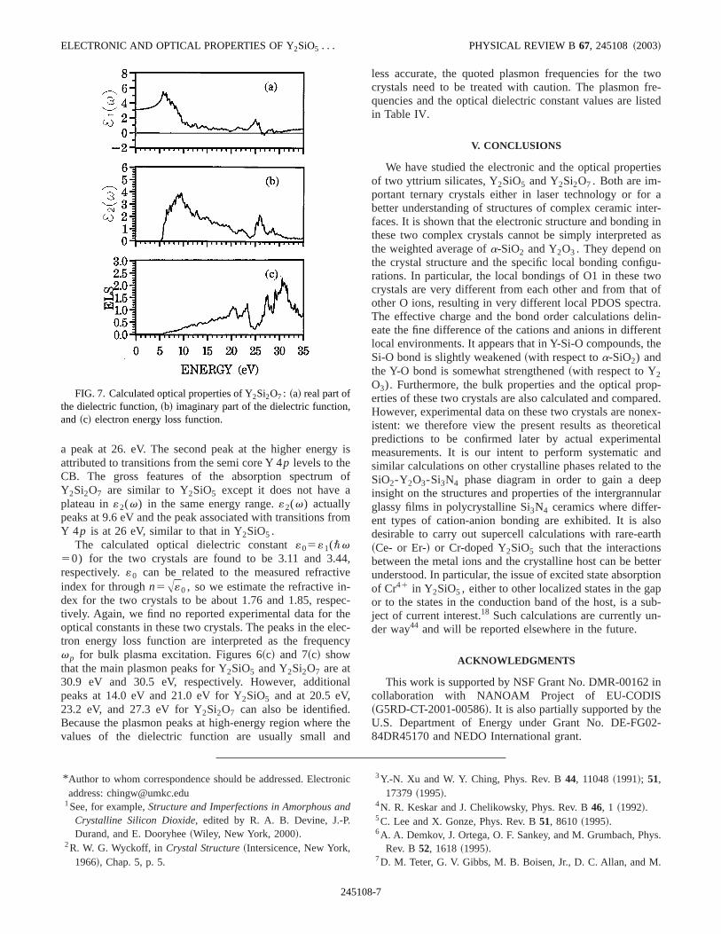
D. Optical properties
The interband optical transitions with all dipole matrelements included were calculated for Y2SiO5 and Y2Si2O7 .To achieve higher accuracy, an extended basis set was uThe imaginary parts of the dielectric functions«2(v) werecalculated first and the real parts«1(v) were obtained fromthe imaginary parts by Kramers-Kronig conversion. The eergy loss functions were obtained from the inverse ofcomplex dielectric function or Im$@«1(v)1i«2(v)#21%.These results are presented in Figs. 6 and 7 for Y2SiO5 andY2Si2O7 respectively. For Y2SiO5 , «2(v) rises swiftly fromthe threshold at 5.0 eV to reach a plateau at about 7.1 estarts to drop at 9.2 eV until around 24 eV: it rises again w
f
FIG. 6. Calculated optical properties of Y2SiO5 : ~a! real part ofthe dielectric function,~b! imaginary part of the dielectric functionand ~c! electron energy loss function.
8-6
y
oa
ro
4ive-ehelenc
a
.
nd
twofre-sted
ties
r ater-g in
as
gu-woof
ra.lin-entthe
p-red.ex-
ticaltalndthe
epular
lsorth
settertionpub--
in
2-
on
nd.
ys.
.
,
ELECTRONIC AND OPTICAL PROPERTIES OF Y2SiO5 . . . PHYSICAL REVIEW B67, 245108 ~2003!
a peak at 26. eV. The second peak at the higher energattributed to transitions from the semi core Y 4p levels to theCB. The gross features of the absorption spectrumY2Si2O7 are similar to Y2SiO5 except it does not haveplateau in«2(v) in the same energy range.«2(v) actuallypeaks at 9.6 eV and the peak associated with transitions fY 4p is at 26 eV, similar to that in Y2SiO5 .
The calculated optical dielectric constant«05«1(\v50) for the two crystals are found to be 3.11 and 3.4respectively.«0 can be related to the measured refractindex for throughn5A«0 , so we estimate the refractive index for the two crystals to be about 1.76 and 1.85, resptively. Again, we find no reported experimental data for toptical constants in these two crystals. The peaks in the etron energy loss function are interpreted as the frequevp for bulk plasma excitation. Figures 6~c! and 7~c! showthat the main plasmon peaks for Y2SiO5 and Y2Si2O7 are at30.9 eV and 30.5 eV, respectively. However, additionpeaks at 14.0 eV and 21.0 eV for Y2SiO5 and at 20.5 eV,23.2 eV, and 27.3 eV for Y2Si2O7 can also be identifiedBecause the plasmon peaks at high-energy region wherevalues of the dielectric function are usually small a
*Author to whom correspondence should be addressed. Electraddress: [email protected]
1See, for example,Structure and Imperfections in Amorphous aCrystalline Silicon Dioxide, edited by R. A. B. Devine, J.-PDurand, and E. Dooryhee~Wiley, New York, 2000!.
2R. W. G. Wyckoff, inCrystal Structure~Intersicence, New York,1966!, Chap. 5, p. 5.
FIG. 7. Calculated optical properties of Y2Si2O7 : ~a! real part ofthe dielectric function,~b! imaginary part of the dielectric functionand ~c! electron energy loss function.
24510
is
f
m
,
c-
c-y
l
the
less accurate, the quoted plasmon frequencies for thecrystals need to be treated with caution. The plasmonquencies and the optical dielectric constant values are liin Table IV.
V. CONCLUSIONS
We have studied the electronic and the optical properof two yttrium silicates, Y2SiO5 and Y2Si2O7 . Both are im-portant ternary crystals either in laser technology or fobetter understanding of structures of complex ceramic infaces. It is shown that the electronic structure and bondinthese two complex crystals cannot be simply interpretedthe weighted average ofa-SiO2 and Y2O3. They depend onthe crystal structure and the specific local bonding confirations. In particular, the local bondings of O1 in these tcrystals are very different from each other and from thatother O ions, resulting in very different local PDOS spectThe effective charge and the bond order calculations deeate the fine difference of the cations and anions in differlocal environments. It appears that in Y-Si-O compounds,Si-O bond is slightly weakened~with respect toa-SiO2) andthe Y-O bond is somewhat strengthened~with respect to Y2O3). Furthermore, the bulk properties and the optical proerties of these two crystals are also calculated and compaHowever, experimental data on these two crystals are nonistent: we therefore view the present results as theorepredictions to be confirmed later by actual experimenmeasurements. It is our intent to perform systematic asimilar calculations on other crystalline phases related toSiO2-Y2O3-Si3N4 phase diagram in order to gain a deinsight on the structures and properties of the intergrannglassy films in polycrystalline Si3N4 ceramics where differ-ent types of cation-anion bonding are exhibited. It is adesirable to carry out supercell calculations with rare-ea~Ce- or Er-! or Cr-doped Y2SiO5 such that the interactionbetween the metal ions and the crystalline host can be bunderstood. In particular, the issue of excited state absorpof Cr41 in Y2SiO5 , either to other localized states in the gaor to the states in the conduction band of the host, is a sject of current interest.18 Such calculations are currently under way44 and will be reported elsewhere in the future.
ACKNOWLEDGMENTS
This work is supported by NSF Grant No. DMR-00162collaboration with NANOAM Project of EU-CODIS~G5RD-CT-2001-00586!. It is also partially supported by theU.S. Department of Energy under Grant No. DE-FG084DR45170 and NEDO International grant.
ic3Y.-N. Xu and W. Y. Ching, Phys. Rev. B44, 11048~1991!; 51,17379~1995!.
4N. R. Keskar and J. Chelikowsky, Phys. Rev. B46, 1 ~1992!.5C. Lee and X. Gonze, Phys. Rev. B51, 8610~1995!.6A. A. Demkov, J. Ortega, O. F. Sankey, and M. Grumbach, Ph
Rev. B52, 1618~1995!.7D. M. Teter, G. V. Gibbs, M. B. Boisen, Jr., D. C. Allan, and M
8-7
.
ud
.a-
rt
in
m.
,
m
m
nly
ris
.
R.
a,
.
oc.
lid
W. Y. CHING, LIZHI OUYANG, AND YONG-NIAN XU PHYSICAL REVIEW B 67, 245108 ~2003!
P. Teter, Phys. Rev. B52, 8064~1995!.8W. Y. Ching and Y.-N. Xu, Phys. Rev. Lett.65, 895 ~1990!.9D. R. Mueller, D. L. Ederer, J. van Ek, W. L. O’Brien, Q. Y
Dong, J. Jia, and T. A. Callcott, Phys. Rev. B54, 15034~1996!.10F. Jollet, C. Noguera, N. Thromat, M. Gautier, and J. P. Dura
Phys. Rev. B42, 7587~1990!.11Y.-N. Xu, Z.-Q. Gu, and W. Y. Ching, Phys. Rev. B56, 14993
~1997!.12H. I. Leonyuk, E. L. Belokoneva, G. Bocelli, L. Righi, E. V
Shvanskii, R. V. Henrykhson, N. V. Kulman, and D. E. Kozhbkhteeva, J. Cryst. Growth205, 361 ~1999!.
13J. Warshaw and R. Roy, Prog. Sci. Technol., Rare Earths1, 203~1961!.
14S. H. Shin, D. Y. Jeon, and K. S. Suh, Jpn. J. Appl. Phys., Pa40, 4715~2001!.
15T. Bottger, Y. Sun, G. J. Reinemer, and R. L. Cone, J. Lum94&95, 565 ~2001!.
16Y. K. Kuo, M. F. Huang, and M. Birnbaum, IEEE J. QuantuElectron.31, 657~1995!; C. Deka, B. H. T. Chai, Y. Shimony, XX. Zhang, E. Munin, and M. Bass, Appl. Phys. Lett.61, 2141~1992!; E. Munin, A. B. Villaverde, X. X. Zhang, and M. Bassibid. 63, 1739~1993!.
17Y.-N. Xu and W. Y. Ching, Phys. Rev. B59, 10530~1999!; W. Y.Ching and Y.-N. Xu,ibid. 59, 12815~1999!.
18W. Y. Ching, Y.-N. Xu, and B. K. Brickeen, Appl. Phys. Lett.74,3755 ~1999!.
19Y.-N. Xu, W. Y. Ching, and B. K. Brickeen, Phys. Rev. B61,1817 ~2000!.
20W. Y. Ching, Y.-N. Xu, and B. K. Brickeen, Phys. Rev. B63,115101~2001!.
21M. Antonia Sainz, P. Moranzo, and M. Isabel Osendi, J. ACeram. Soc.85, 941 ~2002!.
22F. F. Lange, S. C. Singhal, and R. C. Kuznicki, J. Am. CeraSoc.60, 249 ~1977!.
23L. J. Gauckler, H. Hohnke, and T. Y. Tien, J. Am. Ceram. Soc.63,35 ~1980!.
24J. Ito and H. Johnson, Am. Mineral.53, 1940~1968!; K. Liddell
24510
,
1
.
.
.
and D. P. Thompson, Br. Ceram. Trans.85, 17 ~1986!.25The current calculations ona-SiO2 and Y2O3 are the improved
versions over those published in Refs. 3 and 11. They differ oslightly from the earlier results.
26C. Michel, G. Buisson, and E. F. Bertaut, C. R. Acad. Sci., Pa264 ~5!, 397 ~1967!.
27B. A. Maksimov, V. V. Kharotonov, A. Yu, and N. V. Belov, DoklAkad. Nauk BSSR183, 1072~1968!.
28W. Y. Ching, J. Am. Ceram. Soc.71, 3135~1990!.29S.-D. Mo, L. Ouyang, W. Y. Ching, I. Tanaka, Y. Koyama, and
Riedel, Phys. Rev. Lett.83, 5046~1999!.30W. Y. Ching, S.-D. Mo, and L. Ouyang, Phys. Rev. B63, 245110
~2001!.31W. Y. Ching, S.-D. Mo, L. Ouyang, I. Tanaka, and M. Yoshiy
Phys. Rev. B61, 10609~2000!.32W. Y. Ching, S.-D. Mo, Y. Chen, P. Rulis, I. Tanaka, and M
Yoshiya, J. Am. Ceram. Soc.85, 75 ~2002!.33W. Y. Ching, Z. Q. Gu, and Y.-N. Xu, J. Appl. Phys.89, 6883
~2001!.34L. Ouyang, Y.-N. Xu, and W. Y. Ching, Phys. Rev. B65, 113110
~2002!.35W. Y. Ching, Y.-N. Xu, and L. Ouyang, Phys. Rev. B66, 235106
~2002!.36P. Hohenberg and W. Kohn, Phys. Rev.136, B864 ~1964!; W.
Kohn and L. J. Sham, Phys. Rev.140, A1133 ~1965!.37W. Y. Ching, L. Ouyang, and J. D. Gale, Phys. Rev. B61, 8696
~2000!.38Lizhi Ouyang and W. Y. Ching, J. Am. Ceram. Soc.84, 801
~2001!.39R. S. Mulliken, J. Chem. Phys.23, 1833~1955!.40F. D. Murnaghan, Proc. Natl. Acad. Sci. U.S.A.30, 244 ~1944!.41O. Unal and M. Akinc, J. Am. Ceram. Soc.79, 805 ~1996!.42W. R. Manning, O. Hunter, and B. R. Powell, J. Am. Ceram. S
52, 436 ~1969!.43R. M. Hazen, L. W. Finger, R. J. Hemley, and H. K. Mao, So
State Commun.72, 507 ~1989!.44W. Y. Ching et al. ~unpublished!.
8-8


