Embed Size (px)
Citation preview

Electronic transport through Si nanowires: Role of bulk and surface disorder
Troels Markussen,1 Riccardo Rurali,2 Mads Brandbyge,1 and Antti-Pekka Jauho1
1MIC, Department of Micro and Nanotechnology, NanoDTU, Technical University of Denmark, DK-2800 Kgs. Lyngby, Denmark2Departament d’Enginyeria Electrònica, Universitat Autònoma de Barcelona 08193 Bellaterra, Spain
�Received 13 June 2006; revised manuscript received 15 September 2006; published 15 December 2006�
We calculate the resistance and mean free path in long metallic and semiconducting silicon nanowires�SiNW’s� using two different numerical approaches: a real-space Kubo method and a recursive Green’s-function method. We compare the two approaches and find that they are complementary: depending on thesituation a preferable method can be identified. Several numerical results are presented to illustrate the relativemerits of the two methods. Our calculations of relaxed atomic structures and their conductance properties arebased on density functional theory without introducing adjustable parameters. Two specific models of disorderare considered: Unpassivated, surface reconstructed SiNW’s are perturbed by random on-site �Anderson�disorder whereas defects in hydrogen passivated wires are introduced by randomly removed H atoms. Theunpassivated wires are very sensitive to disorder in the surface whereas bulk disorder has almost no influence.For the passivated wires, the scattering by the hydrogen vacancies is strongly energy dependent and forrelatively long SiNW’s �L�200 nm� the resistance changes from the Ohmic to the localization regime withina 0.1-eV shift of the Fermi energy. This high sensitivity might be used for sensor applications.
DOI: 10.1103/PhysRevB.74.245313 PACS number�s�: 73.63.�b, 72.15.Lh, 72.10.Fk
I. INTRODUCTION
Semiconducting nanowires are a very promising buildingblock for future nanoelectronic and nanophotonic applica-tions as witnessed by several recently demonstrateddevices.1–6 Silicon nanowires �SiNW’s� are especially attrac-tive candidates due to their compatibility with conventionalSi technology and due to the accurate control of diameterand electronic properties during synthesis.7 Furthermore, inrecent years SiNW’s have been applied as label-free real-time chemical and biological sensors with very high sensi-tivity and, e.g., capability of single-virus detection.8
Thin SiNW’s with diameters below 5 nm have been syn-thesized by several groups. Recently, Ma et al.9 obtainedvery thin wires grown in the �110� and �112� directions withdiameters down to 1.3 nm and Holmes et al.10 previouslyreported 4–5-nm �100� and �110� SiNW’s. Wu et al.7 re-cently demonstrated that the growth directions depend on thediameter, which can be controlled by the size of a catalyticnanoparticle.11
Concerning theoretical modeling of the structural proper-ties, Rurali and Lorente12 recently showed, using ab initiocalculations, that thin �100� unpassivated SiNW’s could beeither metallic or semimetallic depending on the surface re-construction. In another recent work, Singh et al.13 theoreti-cally studied pristine �110� SiNW’s and found that thesewere indirect band gap semiconductors. Fernández-Serra etal.14 used ab initio calculations to study the surface segrega-tion of dopants in both passivated and unpassivated SiNW’s,and Vo et al.15 very recently used ab initio calculations tosimulate the structural and electronic properties of hydrogen-passivated SiNW’s grown in different directions.
The large surface to bulk ratio in the thin wires impliesthat surface effects such as defects, vacancies, or adatomswill have a large influence on the transport properties. Thiswas experimentally demonstrated by Cui et al.4 showing in-creased mobilities after passivation of surface defects. Also,
electron-phonon scattering might be suppressed in thinwires. Indeed, recent experiments by Lu et al.16 indicatedballistic transport in undoped Si/Ge core-shell wires at roomtemperature with an estimated phonon scattering mean freepath �MFP� lph�500 nm. This might imply that even atroom temperature defects could be the most important scat-tering source, and a thorough understanding of the scatteringprocesses is thus required.
A number of transport calculations have been reported forwires with various diameters. Das and Mizel17 used the Bolt-zmann equation to calculate the carrier mobility in relativethick �d=10–90 nm� GaAs wires, focusing on the diameterdependence. Sundaram and Mizel18 also used the Boltzmannequation to study surface effects on the transport in large-diameter wires. Zheng et al.19 applied a tight-binding modelof a hydrogen-passivated wire and studied the effect of wirethickness on the band gap, effective masses, and transmis-sion.
Real SiNW’s with lengths up to the scale of micrometersconsist of millions of atoms and are likely to have manyrandomly placed defects. To our knowledge, no theoreticalworks concerning SiNW’s, based on ab initio methods andincluding many scattering events, have yet been published.
A calculation of the conductance of a SiNW with manyrandomly positioned defects puts strong requirements on themethod. The quasi-one-dimensional nature of the SiNW’srequires on the one hand an atomistic model taking quantumeffects and charge transfer around the defect into account.On the other hand, the method should be able to treat morethan 105 atoms and include many scattering events due to the�m length of the wires.
In this work, two methods are used to study the effect ofdisorder including many randomly placed H vacancies inH-passivated long SiNW’s. Both methods are based on abinitio calculations and scale linearly with the length of thesample. The first approach uses a relatively recent real-spacemethod developed by Roche and Mayou and co-workers
PHYSICAL REVIEW B 74, 245313 �2006�
1098-0121/2006/74�24�/245313�11� ©2006 The American Physical Society245313-1

over the last decade to study transport properties primarily incarbon nanotubes and quasiperiodic systems.20–28 Themethod is based on the Kubo-Greenwood formalism29,30 re-written in a real-space framework, and we will refer to it asthe Kubo method. The second and more well-known ap-proach is based on the Landauer formula where the conduc-tance is found by recursive calculations of Green’s functions�GF’s�. We will refer to this as the GF method.
The Kubo method was shown to predict the elastic MFPat the Fermi energy in randomly disordered carbon nano-tubes �CNT’s�,24 in agreement with a Fermi’s golden ruleestimate.31 Besides that, we are aware of no comparison withother theoretical methods. One of the primary goals of thispaper is to report such a comparison over several energies.We show that the Kubo and GF methods are in general inqualitative agreement, however with quantitative differencesespecially around band edges. We analyze the pros and consof the two methods and give an assessment of when theyshould be applied and which quantities they can calculate.
The rest of the paper is organized as follows. In Sec. II wesummarize the two numerical methods and describe how aHamiltonian for a long SiNW is constructed from ab initiocalculations. Results concerning both unpassivated as well ashydrogen-passivated SiNW’s are presented in Sec. III. Weend up with a discussion of the applied methods and theresults in Sec. IV.
II. METHODS
A. Real-space Kubo method
In the real-space Kubo method, which is derived from theKubo-Greenwood formula, transport properties are deter-mined by calculating the time propagation of wave packetsin real space. The central quantity is the time- and energy-dependent diffusion coefficient D�E , t�, defined by
D�E,t� =1
t
Tr��X�t� − X�0��2��E − H��Tr���E − H��
, �1�
where X�t� is the position operator along the wire directionwritten in the Heisenberg representation, H is the Hamil-tonian matrix, and the trace Tr���E−H�� is the total elec-tronic density of states �DOS�. Since the Hamiltonian in thecalculations is finite, the energy has a small imaginary parti�, where �5 meV is chosen to scale linearly with thetotal band width and inversely with the system size. Follow-ing Triozon et al.24,32 an efficient evaluation of the traces canbe carried out by using a relative modest number ��10� ofrandom phase states �r�. The coefficients of �r�, �r�j�, withj=−N /2 , . . . ,N /2 where N is the total number of orbitals inthe wire, are initially nonzero only in the central part of thenanowire—i.e.,
�r�j� = � 1�Nr
e2i�r�j�, for − Nr/2 j Nr/2,
0 otherwise, �2�
where r�j� is an independent random number in the interval�0,1� for every �r , j�. Initially, �r�t=0�� is located in the
central part of the wire, and as time evolves it spreads out tothe sides as illustrated in Fig. 1 �top�. In order to avoid scat-tering at the boundaries at large propagation times, the initialrange of �r� must be much smaller than the total system.Typically Nr104 while the total number of orbitals is N105. The number of random phase states needed to accu-rately estimate the traces is not known a priori, and the con-vergence of the results must be checked.
The time evolution of the random phase states can beefficiently computed by expanding the time evolution opera-tor e−iHt/� in the orthogonal set of Chebyshev polynomials.Each term in the traces in Eq. �1� is a local density of statewhich is calculated using a continued fraction technique.33
This is the most time-consuming part of the calculations andinvolves 103 operations with the Hamiltonian for the con-sidered systems to resolve the closely lying energy bands.The convergence of the continued fraction scheme must beseparately verified.
The elastic MFP le�EF� for a given energy E=EF is foundfrom24
le�EF� =max�D�EF,t�,t � 0�
v�EF�, �3�
where v�E� is an energy-dependent effective velocity. For apristine system the electron motion is ballistic and the diffu-sion coefficient increases linearly with time, D�E , t�=v2�E�t,with the slope given by the square of the effective velocity.In Sec. III A and the Appendix we discuss this effective ve-locity in more detail. We note that in the ballistic regime le→� and the “max” in Eq. �3� is not well defined.
The geometry used in the Kubo calculations is sketched inFig. 1 �middle�. Notice that there is no requirement that theHamiltonian be periodic. Nor are there any leads that con-nect to the device region as in the GF method, Fig. 1 �bot-tom�, to be discussed in the next section.
We stress that the time it takes to calculate the diffusioncoefficient at many energies is not much longer than for asingle energy. The reason for this is that the random phasestates contain all energy components and the time evolutionis energy independent. Moreover, the primary numerical taskin the continued fraction scheme is a mapping of the originalHamiltonian to a smaller tridiagonal matrix. This mapping is
FIG. 1. Top: schematic time evolution of a random phase state�r�t�� initially located in the central region of the wire. Middle: thegeometry in the Kubo method consists only of a large device re-gion. Bottom: in the GF approach a device region is connected totwo semi-infinite leads.
MARKUSSEN et al. PHYSICAL REVIEW B 74, 245313 �2006�
245313-2

energy independent, and it is therefore relatively fast to com-pute the MFP for the whole energy spectrum.
B. Recursive Green’s function method
The second numerical method we have applied is basedon the Landauer formalism described in detail in, e.g., Ref.34. The general setup is illustrated in Fig. 2. A device region�D� is connected to a left �L� and right �R� semi-infinite lead.The device area consists of M subcells and is described bythe Hamiltonian HD:
HD =�HD
�1� V1,2 0 . . .
V1,2† HD
�2� V2,3
0 V2,3†
� �
� � HD�M�� . �4�
The subcells are chosen so large that only nearest-neighborcells couple. Generally, the subcells do not need to have thesame size. The leads described by HL and HR, respectively,are assumed to have a semi-infinite structure consisting ofequal unit cells with Hamiltonians H0. The coupling matricesbetween the leads and the device area are denoted VL andVR. The Hamiltonians are calculated with a nonorthogonalbasis set �see Sec. II C� such that for each Hamiltonian ma-trix we also have a corresponding overlap matrix S.
To calculate the length dependent conductance of thewire, we initially find the surface Green’s functionsGL,R
0 �E�= �ESL,R−HL,R�−1 of the isolated leads by a standarddecimation procedure.35 The device area is subsequentlygrown by adding one subcell at a time and calculating theGreen’s function
Gi�E� = �ESD�i� − HD
�i� − L�i��E� − R�E��−1, �5�
where R�E� describes the coupling to the right lead and isdefined through GR
0�E�= �ES0−H0− R�E��−1, and where weassure that the coupling of cell i to lead R is the same as thecell-to-cell coupling within the lead. L
�i��E� also takes thecoupling to the rest of the device area into account and iscalculated from the previous growth step as L
�i��E�= �ESi−1,i
† −Vi−1,i† �G̃i−1�E��ESi−1,i−Vi−1,i�, where G̃i−1�E�
= �ESD�i−1�−HD
�i−1�− L�i−1��E��−1.
In each growth step we calculate the conductance of thewire consisting of the first i subcells as
g�E,Li� =2e2
hTr�Gi
†�E��R�E�Gi�E��L�i��E�� , �6�
where Li is the length of the grown device region, �L�i��E�=
−2 Im� L�i��E��, and likewise for �R�E�. The trace is per-
formed over the states in the device region.Sample averaging is performed over 200 different con-
figurations, giving a mean conductance �g�. The correspond-ing resistance is found as R=1/ �g�. For wire length L��,with � being the localization length, the resistance increaseslinearly as R�L�=R0+R0L / le, defining the MFP le.
36 In thelocalization regime the resistance increases exponentiallyand we calculate the localization length as37
� = − limL→�
2L
�ln g�, �7�
where L has to be so large that � is converged.
C. Constructing the Hamiltonian from ab initio calculations
The atomic and electronic structure of the SiNW’s isfound from ab initio calculations using the density functionaltheory �DFT� package SIESTA.38 Using first-principles calcu-lations it is relatively straightforward to introduce variousdefects such as vacancies, adatoms, or dopants. This is notthe case when using standard tight-binding parameters.
We have used a minimal single-� basis set,39 with fourorbitals �one 3s and three 3p� on the Si atoms and one on theH atoms, to represent the one-electron wave function. Theminimal basis set is applied in order to speed up the subse-quent transport calculations. We have used norm-conservingpseudopotentials of the Troullier-Martins type40 and the gen-eralized gradient approximation41 for the exchange-correlation functional. The calculations are performed on su-percells containing five wire unit cells �see Figs. 3 and 4�.The reciprocal space has been sampled with a converged gridof 1�1�2k points following the Monkhorst-Pack scheme.42
When modeling a defect this is placed in the middle of thesupercell to ensure that the effect of the defect is confined tothe central region and is not affected by the periodicity andthe intercell coupling terms Vi−1,i in Eq. �4� are independentof the specific type of defect. The atomic postions of all theatoms in the unit cell containing the defect and in the twoneighboring unit cells have been fully relaxed, until the
FIG. 2. The device region �D� is divided into M subcells. Thesubcells are so large that they only couple to the nearest-neighborcells. Also, the left �L� and right �R� leads consisting of equal unitcells, described by H0, couple only to the first and last cell of thedevice region, respectively.
FIG. 3. �Color online� Top: schematic illustration of supercellscontaining five unit cells from three different DFT calculations: onepristine wire and two wires with different defects. In the latter thedefects are located in unit cell number 3. The cells number 1 and 5are assumed to be the same in all three calculations. Bottom: a longwire is constructed by joining pieces from the different DFTcalculations.
ELECTRONIC TRANSPORT THROUGH Si NANOWIRES:… PHYSICAL REVIEW B 74, 245313 �2006�
245313-3
maximum force was smaller than 0.04 eV/Å. This is an im-portant point, because the local distortion induced by thedefect can have important consequences on its scatteringproperties.
To model a long �L�100 nm� SiNW with a random dis-tribution of defects �Sec. III B� we perform a full SIESTAcalculation for a pristine wire and for each type of defect.The wire is grown by adding pieces from the different cal-culations, ending up with a wire structure as in Fig. 2 and aHamiltonian as Eq. �4�. The subcells HD
�i� can either be pris-tine parts or contain a defect. In the latter case the subcellconsists of three unit cells with the defect in the middle.Figure 3 illustrates schematically how a wire is built up frompristine parts and from parts containing two different defects.The upper panel symbolizes the periodically repeated super-cells from three different SIESTA calculations: one pristinewire �left� and two wires containing two different defectsplaced in the middlemost unit cell. The first and last unitcells in each calculation are assumed to be the same for boththe pristine wire and the wires containing defects.
Usually when joining pieces from different calculationsthe Fermi energies should be aligned to ensure charge con-servation. However, for the SiNW’s with hydrogen vacan-cies, a dangling bond �DB� state forms in the band gap andpins the Fermi energy, causing a large shift compared to apristine wire. Alignment of the Fermi energies would there-fore lead to an unphysical shift in energies also for sites faraway from the vacancy. We therefore align the Si 3s on-siteenergy instead, taking as reference a fixed Si atom in unitcell number 1.
The minimal basis set implies that we can not expect theconduction bands to be accurately described, and we willthus only focus on the valence bands. Furthermore, theHamiltonian is truncated by removing the smallest elements,while keeping the band structure constant with a tolerance of10−2 eV. This leads to a reduction of nonzero matrix ele-ments of around 80%, and we thus effectively end up with atight-binding-like Hamiltonian.
SIESTA uses a nonorthogonal atomic basis set giving riseto an overlap matrix S. The Kubo method, however, requiresan orthogonal basis set, and the SIESTA output cannot there-fore be used directly for which reason a Löwdin transforma-tion is performed. For each SIESTA calculation the Hamil-tonian H, containing five unit cells described in the
nonorthogonal atomic basis, is mapped to a new one H̃, withan orthogonal basis:
H → H̃ = S−1/2HS−1/2. �8�
In the same way as described above, a long wire is built byextracting parts from both pristine and defected orthogonal-ized Hamiltonians and joining the pieces. The Löwdin trans-formation leads to a longer range of the basis orbitals andthus more nonzero elements in the truncated Hamiltonian.This in turn implies longer calculation times.
D. Fermi’s golden rule
We next compare the two numerical approaches with re-sults obtained using Fermi’s golden rule �FGR�. We considerscattering due to the scattering potential V between unper-turbed Bloch states n ,k� of the pristine wire. The transportrelaxation rate 1 /�n from band n at energy E is found as
1
�n„En�k�…=
2�
�� dk�
2��m
�k�,mVn,k�2 � �1
− cos �kk���„Em�k�� − En�k�…
=4�
��m
�− k�,mVn,k�2nm�E�
=4�
��2�
m,j�−k�,m�j�2�k,n�j�2nm�E� ,
where the m summation is over bands and the j summationruns over sites in one unit cell. �k,n�j�= �j k ,n� is the ampli-tude of the Bloch state at site j, nm�E� is the DOS corre-sponding to band m, and the energy of the final state fulfillsEm�−k��=En�k�=E. �kk� is the angle between the initial andfinal wave vectors. Only scattering from a forward- to abackward-propagating state contributes to the rate—i.e.,�kk�=−�—yielding a factor of 2. The perturbing potential Vis for the Anderson on-site disorder �Sec. III A� simply adiagonal matrix with the diagonal elements being randomnumbers in a given interval with variance �2 �see below�,and the overbar denotes an average over different configura-tions of V. The MFP for electrons in band n is calculated as
ln�E� = vn�E��n�E� , �9�
where vn�E� is the group velocity at energy E in the nthband. We calculate the total MFP as the mean value from theindividual contributions from the bands:
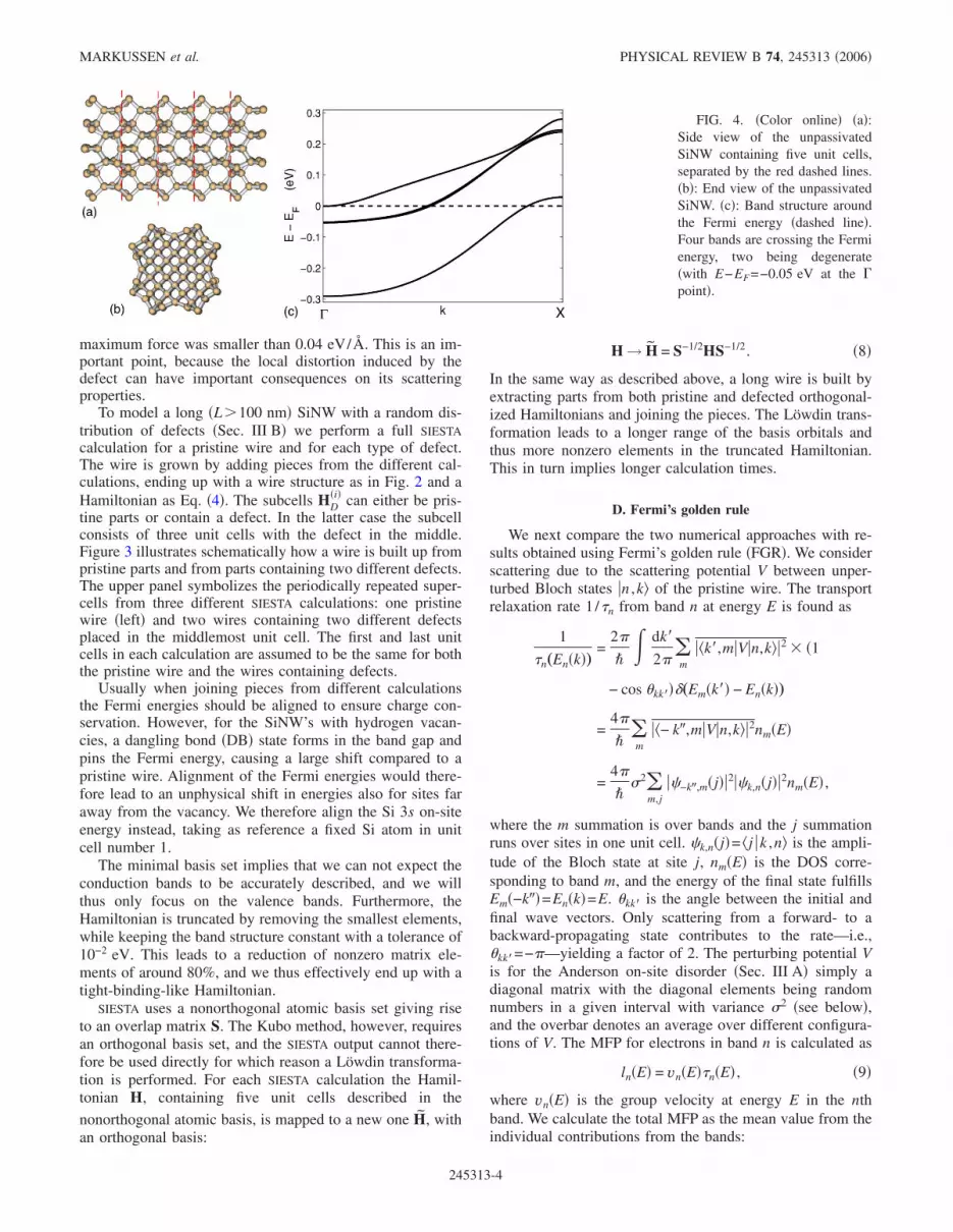
FIG. 4. �Color online� �a�:Side view of the unpassivatedSiNW containing five unit cells,separated by the red dashed lines.�b�: End view of the unpassivatedSiNW. �c�: Band structure aroundthe Fermi energy �dashed line�.Four bands are crossing the Fermienergy, two being degenerate�with E−EF=−0.05 eV at the �point�.
MARKUSSEN et al. PHYSICAL REVIEW B 74, 245313 �2006�
245313-4

le�E� =1
N�E��n
ln�E� , �10�
where N�E� is the number of bands at energy E.
III. RESULTS
A. Surface-reconstructed wires
The first structures we consider are unpassivated, surfacereconstructed SiNW’s as illustrated in Fig. 4 showing a sideview �a� and a cross-section view �b� of a wire containing 5unit cells, separated by the red dashed lines in the upperpanel. This structure was recently studied by Rurali andLorente12 using DFT calculations. There are 57 atoms in oneunit cell, the diameter is 1.5 nm, and the length of the unitcell in the growth direction is 0.55 nm. Notice that the struc-ture at the surface differs significantly from the bulk of thewire. Reference 12 showed that this particular surface struc-ture makes the wire metallic, which is evident in Fig. 4�c�,showing the band structure around the Fermi energy �markedby the dashed line�. Four bands are crossing the Fermi level�two being degenerate�.
To further investigate the metallic surface states and tocompare the Kubo and GF methods we add random on-sitenoise to either the surface atoms only or to the bulk atomsonly. The relevant diagonal elements in the Hamiltonian arethus changed according to
Hii → Hii + �i, �11�
where �i takes values with equal probability in the interval�−�� /2 ;�� /2� with �� being the disorder strength. The uni-form disorder distribution has variance �2= ����2 /12. ThisAnderson model for electronic disorder is simple and widelyapplied; very recently, Zhong and Stocks43 used it to modelsurface disorder in shell-doped nanowires. Whether thissimple model adequately describes physical defects merits aseparate discussion, given at the end of Sec. III B.
Figure 5 shows D�E , t� at E−EF=0.1 eV,44 revealing thatthe bulk disorder �dashed black� has a very small effect onthe transport properties, yielding an almost linearly increas-
ing diffusion coefficient D�E , t�=v2�E�t, a characteristic fea-ture of ballistic transport, as discussed in Sec. II A. The sur-face disorder �solid red�, on the other hand, leads to diffusivetransport with D�E , t� almost constant for t�150 fs. Thepronounced differences of the surface- and bulk-disorderedsystems show that the conduction around the Fermi energyalmost entirely takes place along the surface atoms, in quali-tative agreement with the conclusions drawn in Ref. 12. Thetwo additional curves show �veff
�1��2t �dotted green� and �veff�2��2t
�dash-dotted blue�, where veff�1�=��mnmvm
2 /�mnm
=0.112 nm/fs and veff�2�=�mnmvm /�mnm=0.101 nm/fs are
calculated from the band structure, Fig. 4�c�, according to thediscussion in the Appendix. The band velocities are v1,2=0.157 nm/fs for the degenerate band and v3=0.059 nm/fsfor the highest-lying band. It is evident that the effectivevelocity calculated in the Kubo method from the slope of thelinearly increasing diffusion curve is very close to veff
�1� andnot veff
�2�. As shown in the Appendix this would lead to anoverestimated conductance of a pristine wire when this iscalculated as described in the Appendix A and Ref. 23.
Using Eq. �3� the MFP for the surface-disordered systemis found to be le=6.4 nm. Using the velocity veff
�1� we find themean free time �= le /veff
�1�=57 fs which is approximately halfof the time where the diffusion curve levels off.
The total length of the SiNW’s in the Kubo calculations isL=825 nm, corresponding to 1500 unit cells. Even thoughthe group velocity around the Fermi energy is 0.1 nm/fsand the wave packets thus only propagate 30 nm in the300 fs shown in Fig. 5, there are higher velocities at otherenergies. Moreover, at other energies where the MFP islonger the propagation time must also be longer to reach theflat plateau in the diffusion curve. In order to avoid the wavepacket being reflected at the ends of the wire at long propa-gation times, which affects the calculated diffusion, we findthat very long wires are needed.
Figure 6�a� shows the MFP le�E� versus energy calculatedusing both the Kubo method �solid blue� and the recursiveGF approach �black squares�. The dashed red line is an ana-lytical estimate obtained using FGR. The disorder strength is��=0.4 eV and only the surface atoms are perturbed. TheKubo and FGR results are obtained with a fine energy reso-lution whereas the GF results are calculated only for rela-tively few, discrete energies, illustrating the advantages inthe Kubo method in calculating properties at many energiesin one calculation.
Generally all three methods agree qualitatively and in theinterval −0.1 eV�E�0.2 eV the results are even quantita-tively consistent. In this energy range several bands exist�see Fig. 4�c�� and thus there are more possible backscatter-ing processes giving a larger scattering rate and thus ashorter MFP. Notice that lowering the mean free path doesnot necessarily mean reducing the conductance, because wealso have more charge-carrying states.
Around the band edges at E=−0.09 eV the MFP calcu-lated with FGR drops sharply whereas the values obtainedwith the GF and Kubo methods drop more slowly. This dif-ference is caused by the relatively large disorder strength��=0.4 eV, which broadens the DOS and smears out thesharp features. For smaller disorder strengths the GF results
FIG. 5. �Color online� Time-dependent diffusion coefficient atE−EF=0.1 eV. The bulk disorder has little effect and the transportis ballistic. The edge-disordered system shows diffusive behaviorwith a constant diffusion coefficient for t�150 fs.
ELECTRONIC TRANSPORT THROUGH Si NANOWIRES:… PHYSICAL REVIEW B 74, 245313 �2006�
245313-5

resemble the FGR values more, which is illustrated in thelower panel in Fig. 6. The figure shows, on a logarithmicscale, the MFP versus inverse disorder strength, 1 /��, atthree different energies. The points are obtained with the GFmethod, while the lines are obtained using FGR. For weakdisorder, the GF results scales as le� �1/���2 in accordancewith FGR, whereas the GF results for strong disordered sys-tems deviate from the �1/���2 dependence. In this regimethe first-order perturbation applied in FGR does not fullysuffices and reliable results must be obtained with moreelaborate approaches such as the GF method.
Around 0.24 eV, the Kubo method fails to find the pro-nounced peak obtained with both the GF method and FGR.This difference is probably caused by two effects. The firstreason is again a broadened DOS, since the GF results showa similar deviation from the FGR values as seen around E=−0.09 eV. The second and more important reason for thedifferences is due to numerical inaccuracies in calculatingthe density of states in the Kubo method. The inaccuraciesare especially important around van Hove singularities at thesubband edges. E=0.24 eV marks the band edge for the twodegenerate bands, and due to the finiteness of the systemconsidered in the Kubo calculation, the van Hove peaks inthe DOS will unavoidably have decaying tails at larger ener-gies. This implies that the calculated density of states will betoo large causing D�E , t� and thus le to be correspondinglysmaller. The energy separation between the two subbandedges around E=0.24 eV is only 0.05 eV, which is lessthan 0.3% of the total bandwidth, W�20 eV. This makes itnumerically difficult to resolve the detailed features with thecontinued fraction technique used by the Kubo method.
B. Passivated wires
The surface-reconstructed SiNW’s are both physically andtechnologically exciting, but probably also very fragile ob-jects, since small changes in the surface such as defects oradatoms presumably will change the performance drastically.Moreover, the wires produced are most often surface passi-vated by either SiOx or hydrogen, and the focus in this sec-tion will be on such wires. The passivated wires are semi-conducting, often with a direct band gap that increases forsmall diameters.9,19,45 The simplest way to model surface-passivated wires is to add hydrogen atoms to the surfacesuch that all the Si dangling bonds are passivated. Such wiresresemble qualitatively those reported by Ma et al.9
Figure 7 shows the cross section of the wire �a�. The unitcell contains 57 Si atoms and 36 H atoms labeled with anumber from 1 to 36 as indicated in Fig. 7�a�. The band gapis found to be 2.84 eV.46
To investigate the influence of surface defects we intro-duce hydrogen vacancies. The vacancies are labeled corre-spondingly to the removed hydrogen atoms. Note that due tosymmetry, there are only five topologically different vacan-cies. The conductances of wires with only a single vacancy,corresponding to one of the H atoms 1–3 being removed, areshown in Fig. 7�b� for energies close to the valence bandedge �E=0 eV�. Clearly, vacancies 1 and 2 scatter the most,the reason probably being that the wave function �for thepristine wire� has a pronounced larger weight on these Hatoms. Notice that, for energies −0.15 eV�E�−0.05 eV,
FIG. 6. �Color online�. �a�: mean free path le vs energy E−EF
for ��=0.4 eV. The solid line is obtained with the Kubo method,and the GF results are marked by squares while the dashed lineshows the FGR results. GF results are average values for 200 dif-ferent samples while the Kubo results are mean values of 10 differ-ent samples. �b�: scaling of le vs 1/�� shown on a logarithmicscale. Circles, squares, and triangles are calculated with GF whilethe lines are obtained using FGR at the same energies.
FIG. 7. �Color online� �a�: cross section of the H-passivatedwire. �a�: energy-dependent conductance of a pristine wire and ofwires containing a single vacancy of number 1–3.
MARKUSSEN et al. PHYSICAL REVIEW B 74, 245313 �2006�
245313-6

one channel is almost completely closed by vacancy 1. Va-cancies 3–5 give almost the same conductances.
We model a wire with randomly missing hydrogen atomsby performing a SIESTA calculation for each possible vacancyposition �one of the 36 H atoms is removed� and addingpieces from the different calculations. We measure the va-cancy concentration by the average distance �dH� in the wiredirection between two vacancies. Each unit cell can onlycontain one vacancy, thus setting a lower limit for �dH� at theunit cell length, a=0.56 nm. The MFP for �dH�=5.6 nm cal-culated with the GF method is shown in Fig. 8 �solid line�,revealing a strong energy dependence. In the interval−0.15 eV�E�−0.05 eV, we find le50 nm, while for en-ergies around −0.35 eV the MFP in on the order of 1 �m.Comparing with estimated phonon scattering MFP’s of morethan 500 nm,16 the application of the elastic scattering modelapplied in this work is justified for most of the energies.Moreover, at several energies the vacancy scattering mightbe the dominant even at room temperature. However, aroundthe peak at E=−0.4 eV where the calculated MFP’s exceeds1 �m, other scattering sources are likely to dominate.
Assuming that all bands at a given energy have the samereflection probability, Ri�E�= �T0�E�−Ti�E�� /T0�E�, where T0
is the total transmission of a pristine wire and Ti is the totaltransmission through a wire containing a single vacancy withnumber i �shown in Fig. 7�, the MFP in a wire with onlyvacancies of type i can be estimated as le
�i��E�= �dH�i�� /Ri�E�,
where �dH�i�� is the average distance between vacancies of
type i. The total MFP can be estimated using Matthiessen’s
rule, such that l̃e−1=�i�le
�i��−1, and the result is shown in Fig. 8as the dash-dotted line. It is evident that the simple estimate,which ignores interference effects between successive scat-terers, accurately reproduces the GF results found by sampleaveraging over vacancy configurations.
The Kubo method requires a Hamiltonian describing awire that is longer than the largest mean free path in order toavoid boundary effects. As seen from Fig. 8 we thereforeneed a wire of length L�1500 nm consisting of more than3000 unit cells and thus N�8�105 orbitals. In our currentimplementation this causes computer memory problems andwe have not been able to obtain reliable results with theKubo method for the vacancy scattering.
We next examine whether the vacancies effectively can bemodeled by adding Anderson disorder. The calculated MFPfor a surface disordered wire—i.e., with no vacancies butrather on-site disorder at all orbitals at the surface Siatoms—is shown in Fig. 8 �dashed red line�.
For a disorder strength ��=1.3 eV the Anderson modelfits the vacancy results at energies E�−0.35 eV, althoughthe peak around E=−0.05 eV is much less pronounced. Thesmall shift of the peaks around E=−0.23 eV and E=−0.05 eV is due to a broadened DOS in the Anderson-disordered wires. For energies below −0.35 eV, the Ander-son model deviates significantly from the vacancy results.The pronounced peak in the MFP is not found in the Ander-son model which gives almost constant values up to a factorof 3 lower than the vacancy results. Besides a broadenedDOS, the differences probably arise because the Andersonmodel is a too simple model, not capturing all the physics.Since the Anderson disorder only reproduces the vacancyresults at some energies, we conclude that the effects of va-cancies cannot accurately be modeled by simple on-site dis-order. Moreover, the value of the disorder strength, ��, hasno clear connection to an actual vacancy concentration.
Figure 9 shows the length-dependent resistance for threedifferent energies at vacancy concentration corresponding to�dH�=2.8 nm. For length L�200 nm the resistance increaseslinearly at all energies, with the slope determining the MFP.For the curves in the figure a linear regression fit is per-formed for the initial part of the curves with L�50 nm andthe MFP is extracted using the relation R�L�=R0+R0L / le.For the curves in the figure we obtain a MFP of 199 nm,27 nm, and 39 nm at the energies −0.3 eV, −0.15 eV, and−0.03 eV, respectively. For other vacancy concentrations andother energies the linear fit should be performed over anotherlength range to ensure that it is confined to the linear part ofthe R vs L curve. Note that at E=−0.03 eV there is only one
FIG. 8. �Color online� Mean free path vs energy for a concen-tration of vacancies corresponding to �dH�=5.6 nm. The solid blackline corresponds to wires containing all possible vacancies. Thedash-dotted blue line is obtained using Matthiessen’s rule forsingle-scattering events and the dashed red curve corresponds to awire with Anderson disorder ���=1.3 eV�.
FIG. 9. �Color online� Length-dependent resistance at the ener-gies E=−0.3 eV �dashed blue line�, E=−0.15 eV �dash-dottedgreen line�, and E=−0.03 eV �solid red line�. The average distancebetween vacancies is �dH�=2.8 nm. The inset shows the scaling ofle vs average distance �dH� between vacancies at the same threeenergies as above.
ELECTRONIC TRANSPORT THROUGH Si NANOWIRES:… PHYSICAL REVIEW B 74, 245313 �2006�
245313-7

conducting channel �cf. Fig. 7�b�� and the contact resistanceis thus R0=h /2e2. The inset shows the scaling of le vs �dH� atthe same three energies as in the main figure. The points arecalculated with the GF method and the lines are linear fits,clearly revealing a linear relationship between the MFP andthe average intervacancy distance. For length L�200 nm theresistance corresponding to E=−0.15 eV �dash-dotted greenline� starts to increase exponentially, thus entering the local-ization regime. The localization length at this energy is �=110 nm—i.e., approximately 4 times longer than the MFP.Although there are only three channels at E=−0.15 eV, theresults are roughly in agreement with the general rule �Nle, where N is the number of conducting channels. Withinthe energy interval −0.225eV�E�−0.06 eV where N=3 wefind that the ratio � / le varies between 3 at high energies and5.6 at lower energies. The localization length can thus withina factor of 2 also be estimated from Matthiessen’s rule.
IV. DISCUSSION
In this paper we have studied electronic transport inSiNW’s and calculated the influence of disorder on the meanfree path. Our model is subject to a number of limitationsand approximations. We apply a single-electron model andconsider the linear response regime. Moreover, the minimalbasis set may limit the accuracy. Also the spin-orbit couplingis not included which is necessary to describe the detailsaround the valence band edge in bulk Si. Compared to theexperimentally realized SiNW’s, the wires considered hereare quite thin although comparable to the wires reported inRef. 9. The SiNW structures used in this paper have rounded,rather than perfectly square angles. It has been proposed inthe literature47–49 that smooth angles would be favored dur-ing the growth process with respect to the sharp angles thatnaturally arise from the square symmetry of the �100� cleav-age plane. The topic has been discussed at some detailselsewhere49 for surface-reconstructed wires, concluding thatat nanometric diameters no clear difference emerges. At thesame time the electronic structure seems to be only margin-ally affected. Since all calculations in this work are per-formed on relaxed structures fully based on ab initio calcu-lations without any use of fitting parameters, we expect, inspite of all the limitations, to capture the correct trends in thetransport characteristics.
A. Methods
Two numerical methods were applied and compared toeach other: a real-space Kubo method and a recursiveGreen’s-function method. The two approaches each havetheir advantages: In calculating the MFP at many energies,the Kubo method is advantageous, since the diffusion isreadily found at many energies in a single calculation,whereas the GF method requires a full calculation at eachenergy. If the focus is on a few energies but many differentdisorders, the GF method is the preferred choice. For metal-lic systems, where one mainly is interested in the propertiesaround the Fermi level, the GF method thus seems to be themethod of choice—the parallel computation of many ener-
gies in the Kubo method is not needed. The Kubo methodseems more applicable to semiconducting systems, since it isphysically possible to move the Fermi level with a gate volt-age, thereby scanning several energies.
The Kubo method requires a Hamiltonian describing awire that is longer than the largest MFP in the consideredenergy range. For the weakly disordered wires with longMFP’s we need wires of length L�1 �m containing morethan 105 atoms, resulting in very large matrices. In our cur-rent implementation this causes memory problems and theKubo method failed to converge for the H-passivatedSiNW’s. The GF method, on the other hand, involves onlycalculations with the small subcell Hamiltonians and it suf-fices to consider wires grown to a length L�50 nm to get anaccurate estimate of the initially linear resistance versuslength curve �cf. Fig. 9�. Moreover, it proved to be numeri-cally difficult to resolve the detailed features in the energyspectrum with the Kubo method, which led to erroneous re-sults near band edges. The difficulties arise because the Kubomethod does not take any semi-infinite periodic leads intoaccount as in the GF method. There, the DOS is readilycalculated to arbitrary accuracy from the surface Green’sfunction GL
0 by using the periodic structure of the leads.However, the absence of periodic leads in the Kubo methodcan also be a great advantage since it allows one to studynonperiodic systems such as incommensurable multiwalledcarbon nanotubes.24
The growth procedure in the GF method involves inver-sions of the relatively small matrices describing the subcells.For thin wires as those considered in this work, with N250 orbitals in each unit cell, the inversion step is not acritical issue. However, for thicker wires the number of or-bitals increases quadratically, and due to as O�N3� scaling ofthe inversion step, the whole procedure scales as O�d6�, withd being the wire diameter. On contrary, the Kubo methodscales linearly with the number of orbitals and, thus, asO�d2�.
For systems with a periodic structure, as the SiNW’s con-sidered here, we generally find the GF method to be thepreferred choice, given that a rough energy resolution is suf-ficient. Thicker wires with relatively short MFP’s favor theuse of the Kubo approach.
B. Results
In unpassivated, surface-reconstructed wires, Andersondisorder was added to the surface atoms, affecting the trans-port properties significantly. Disorder in the bulk had, on theother hand, no significant influence.
In hydrogen-passivated wires surface disorder was intro-duced by randomly removed hydrogen atoms. We find that itsuffices to consider single-scattering events and adding theindividually calculated MFP’s to an effective MFP by apply-ing Matthiessen’s rule. Using the rule �Nle, where N is thenumber of conducting channels, the localization length canbe estimated within a factor of 2. However, an accurate de-termination of � seems to require full calculations on longwires with many randomly placed H vacancies as opposed toonly considering single-scattering events. It was further
MARKUSSEN et al. PHYSICAL REVIEW B 74, 245313 �2006�
245313-8

shown that an attempt to model the vacancies with an effec-tive Anderson disorder gave satisfactory values for energiesclose to the valence band edge but failed to reproduce thevacancy results at lower energies.
The MFP was shown to be strongly energy dependent,and for relatively long wires the resistance can be changedby orders of magnitude within a 0.1-eV shift of the Fermienergy, thus causing a transition from the diffusive �Ohmic�regime to the localization regime. The strong energy depen-dence might be utilized in sensor applications where thepresence of a single virus acts as a local gate shifting theFermi energy.8 This could possibly cause a transition fromthe Ohmic to the localization regime, thus changing the re-sistance of the wire dramatically. However, more carefulwork has to be done before firm conclusions can be stated.
For relatively strong disordered wires, the MFP is wellbelow 500 nm for a large energy range. Compared to esti-mated phonon scattering MFP’s of more than 500 nm,16 theelastic scattering model applied in this work is justified.Comparing the results obtained in this work with the esti-mated long phonon MFP we suggest that impurity and defectscattering could be the dominant scattering source even atroom temperature.
ACKNOWLEDGMENTS
We thank H. Smith and N. Lorente for discussions and theDanish Center for Scientific Computing �DCSC� for provid-ing computer resources. T.M. thanks the Oticon Foundationfor financial support. R.R. acknowledge financial support ofthe Ministerio de Educación y Ciencia through the Juan de laCierva programme.
APPENDIX: SIMPLE DOUBLE-CHAIN MODEL
In this appendix we illustrate the difficulties in calculatingthe group velocity in the Kubo method. The problem is most
pronounced near band edges when more bands are present.We consider a model consisting of two infinite parallel
chains as shown in Fig. 10 �a�. Only nearest-neighbor inter-actions are taken into account. The tight-binding parametersare �1 and �2 for hopping between and along the chains,respectively. The distance between two atoms in the samechain is called a. In the Fourier domain the Hamiltonian is
H�k� = ��0 + 2�1 cos�ka� �2
�2 �0 + 2�1 cos�ka�� , �A1�
where �0 is the on-site energy. The eigenvalues are
E±�k� = �0 + 2�1 cos�ka� ± �2, �A2�
and the band structure is shown in Fig. 10 �b� with �0=0 and�1=�2. The density of states and the group velocities for thetwo bands are found as n±=1/ �2���E±�k� /�k−1 and v±
=1/ ����E±�k� /�k.The problems in the Kubo method are clearest illustrated
by calculating the conductance. Following Ref. 23 we startout from an Einstein-like conductivity ��E , t�=e2n�E�D�E , t�, where n�E� is the total electronic density of
FIG. 10. �Color online� �a�: model system. We consider onlynearest-neighbor interaction with the tight-binding parameters �1
and �2 corresponding to hopping in the chain direction and in per-pendicular direction, respectively. The on-site energy is �0. �b�:band structure for the two bands separately. Notice the definition ofthe energies E1−E4.
FIG. 11. �Color online�. �a�: the numerically calculated conduc-tance �dash-dotted black line� is plotted together with the two ana-lytical results g�1��E�, Eq. �A6� �dashed blue line� and g�2��E�, Eq.�A7� �solid red line�. �b�: zoom-in around E=E3, showing thatg�1��E� closely resembles the numerical result.
ELECTRONIC TRANSPORT THROUGH Si NANOWIRES:… PHYSICAL REVIEW B 74, 245313 �2006�
245313-9

states. The conductance of a sample of length L is found asg�E�=��E ,�� /L, where � is the time is takes a wave packetto spread out by an amount equal to L—i.e., implicitly givenby the relation L=�X2�E ,��, where X2�E , t�= tD�E , t�. Atpresent we consider only a pristine system where the electronpropagation is ballistic with X2�E , t�=v2�E�t2, and the con-ductance thus becomes
g�E� = e2n�E�v�E� . �A3�
We calculate the diffusion coefficient as given by Eq. �1�.In the energy interval E� �E2 ;E3� there are two bands andthe ��E−H� projects the states in the trace into a linear com-bination of the eigenstates from the two bands. We can there-fore rewrite Eq. �1� as
D�E,t� =1
t
n+�E�X+2�E� + n−�E�X−
2�E�n+�E� + n−�E�
, �A4�
where X±2�E�= �v±�E�t�2 is the spread of wave packets be-
longing to each band. Defining an effective velocity as �forclarity we omit the explicit energy dependence�
veff�1� =�n+v+
2 + n−v−2
n+ + n−, �A5�
the diffusion coefficient becomes D�E , t�= �veff�1��2 / t. Using
Eq. �A3� the conductance becomes
g�1��E� = e2�n+ + n−��n+v+2 + n−v−
2
n+ + n−, �A6�
in disagreement with the correct result. The conductanceshould rather be
g�2��E� = e2�n+v+ + n−v−� , �A7�
which is obtained if we instead of the effective velocity, veff�1�
in Eq. �A5� use the average velocity
veff�2� =
n+v+ + n−v−
n+ + n−. �A8�
Figure 11 �a� shows the two analytical expressions for theconductances g�1��E� �solid red line� and g�2��E� �dashed blueline� together with the numerical result �dash-dotted blackline� obtained using the Kubo method and time propagation;the lower panel shows an expanded view around E=E3.
It is evident that g�1��E�, Eq. �A6�, resembles the numeri-cal result very much. Especially we find the same peaks inthe conductance around the band edges. The tail in the Kuboconductance is due to the finiteness of the system and reflectsthe imaginary energy i� used in the continued fraction tech-nique. Rewriting the effective velocity �A5� as
veff�1� =
��n+v+ + n−v−�2 + n+n−�v+ − v−�2
n+ + n−, �A9�
we see that the reason why we observe peaks in the conduc-tance is a mixing of the two densities of states given bythe second term in the numerator. This mixing is an inherentfailure in the numerical calculation of the diffusioncoefficient.
1 Y. Cui and C. M. Lieber, Science 291, 851 �2001�.2 M. S. Gudiksen, L. J. Lauhon, J. Wang, D. C. Smith, and C. M.
Lieber, Nature �London� 415, 617 �2002�.3 L. Samuelson, Mater. Today 6, 22 �2003�.4 Y. Cui, D. Wang, W. U. Wang, and C. M. Lieber, Nano Lett. 3,
149 �2003�.5 L. Samuelson et al., Physica E �Amsterdam� 25, 313 �2004�.6 Y. Wu, C. Yang, W. Lu, and C. M. Lieber, Nature �London� 430,
61 �2004�.7 Y. Wu, Y. Cui, L. Huynh, C. Barrelet, D. Bell, and C. Lieber,
Nano Lett. 4, 433 �2004�.8 F. Patolsky and C. M. Lieber, Mater. Today 8, 20 �2005�.9 D. D. D. Ma, C. S. Lee, F. K. Au, S. T. Tong, and S. T. Lee,
Science 299, 1874 �2003�.10 J. D. Holmes, K. Johnston, R. C. Doty, and B. A. Korgel, Science
287, 1471 �2000�.11 Y. Cui, L. J. Lauhon, M. S. Gudiksen, J. Wang, and C. M. Lieber,
Appl. Phys. Lett. 78, 2214 �2001�.12 R. Rurali and N. Lorente, Phys. Rev. Lett. 94, 026805 �2005�.13 A. K. Singh, V. Kumar, R. Note, and Y. Kawazoe, Nano Lett. 5,
2302 �2005�.14 M. V. Fernandez-Serra, C. Adessi, and X. Blase, Phys. Rev. Lett.
96, 166805 �2006�.15 T. Vo, A. J. Williamson, and G. Galli, Phys. Rev. B 74, 045116
�2006�.16 W. Lu, J. Xiang, B. P. Timko, Y. Wu, and C. M. Lieber, Proc.
Natl. Acad. Sci. U.S.A. 102, 10046 �2005�.17 K. K. Das and A. Mizel, J. Phys.: Condens. Matter 17, 6675
�2005�.18 V. S. Sundaram and A. Mizel, J. Phys.: Condens. Matter 16, 4697
�2004�.19 Y. Zheng, C. Riva, R. Lake, K. Alam, T. B. Boykin, and G.
Klimeck, IEEE Trans. Electron Devices 52, 1097 �2005�.20 S. Roche, Phys. Rev. B 59, 2284 �1999�.21 S. Roche and D. Mayou, Phys. Rev. Lett. 79, 2518 �1997�.22 D. Mayou, Phys. Rev. Lett. 85, 1290 �2000�.23 S. Roche and R. Saito, Phys. Rev. Lett. 87, 246803 �2001�.24 F. Triozon, S. Roche, A. Rubio, and D. Mayou, Phys. Rev. B 69,
121410�R� �2004�.25 S. Latil, S. Roche, D. Mayou, and J.-C. Charlier, Phys. Rev. Lett.
92, 256805 �2004�.26 S. Roche, J. Jiang, F. Triozon, and R. Saito, Phys. Rev. B 72,
113410 �2005�.27 S. Roche, J. Jiang, F. Triozon, and R. Saito, Phys. Rev. Lett. 95,
MARKUSSEN et al. PHYSICAL REVIEW B 74, 245313 �2006�
245313-10

076803 �2005�.28 S. Latil, S. Roche, and J.-C. Charlier, Nano Lett. 5, 2216 �2005�.29 R. Kubo, J. Phys. Soc. Jpn. 12, 570 �1957�.30 D. Greenwood, Proc. Phys. Soc. London 71, 585 �1958�.31 C. T. White and T. N. Todorov, Nature �London� 393, 240
�1998�.32 F. Triozon, J. Vidal, R. Mosseri, and D. Mayou, Phys. Rev. B 65,
220202�R� �2002�.33 R. Haydock, V. Heine, and M. Kelly, J. Phys. C 5, 2845 �1972�.34 T. N. Todorov, Phys. Rev. B 54, 5801 �1996�.35 M. Lopez-Sancho, J. Lopez-Sancho, and J. Rubio, J. Phys. F:
Met. Phys. 14, 1205 �1984�.36 S. Datta, Electronic Transport in Mesoscopic Systems �Cambridge
University Press, Cambridge, England, 1995�.37 B. Kramer and A. MacKinnon, Rep. Prog. Phys. 56, 1469 �1993�.38 J. M. Soler, E. Artacho, J. D. Gale, A. García, J. Junquera, P.
Ordejón, and D. Sánchez-Portal, J. Phys.: Condens. Matter 14,2745 �2002�.
39 E. Artacho, D. Sánchez-Portal, P. Ordejón, A. García, and J. M.Soler, Phys. Status Solidi B 215, 809 �1999�.
40 N. Troullier and J. L. Martins, Phys. Rev. B 43, 1993 �1991�.
41 J. P. Perdew, K. Burke, and M. Ernzerhof, Phys. Rev. Lett. 77,3865 �1996�.
42 H. J. Monkhorst and J. D. Pack, Phys. Rev. B 8, 5747 �1973�.43 J. Zhong and G. M. Stocks, Nano Lett. 6, 128 �2006�.44D�E , t� is calculated slightly above the Fermi energy in order to
avoid the numerical difficulties at E=EF, where a band edgeoccur.
45 X. Zhao, C. M. Wei, L. Yang, and M. Y. Chou, Phys. Rev. Lett.92, 236805 �2004�.
46 The calculated band gap is larger than found in Ref. 50 for asimilar structure using a plane-wave DFT method. The band gapreduces to 1.66 eV when using a double-� polarized basis set,in qualitiative agreement with the plane-wave results of Ref. 50�the residual difference must be attributed to the slight differ-ences in the wire structures�.
47 S. Ismail-Beigi and T. Arias, Phys. Rev. B 57, 11923 �1998�.48 Y. Zhao and B. I. Yakobson, Phys. Rev. Lett. 91, 035501 �2003�.49 R. Rurali and N. Lorente, Nanotechnology 16, S250 �2005�.50 A. K. Singh, V. Kumar, R. Note, and Y. Kawazoe, Nano Lett. 6,
920 �2006�.
ELECTRONIC TRANSPORT THROUGH Si NANOWIRES:… PHYSICAL REVIEW B 74, 245313 �2006�
245313-11


![Band structure of Si/Ge core-shell nanowires along [110] direction modulated by external uniaxial strain](https://img.pdfslide.net/doc/110x75/63444aeb596bdb97a90864a5/band-structure-of-sige-core-shell-nanowires-along-110-direction-modulated-by.jpg)


