Embed Size (px)
Citation preview
Biofunctionalization of Si nanowires using a solution based technique Elissa H. Williams*,a,b,c, Albert V. Davydova, Vladimir P. Oleshkoa, Nancy J. Lina, Kristen L. Steffensa, Amy K. Manocchid, Sergiy Krylyuka,e, Mulpuri V. Raoc, and John A. Schreifelsb
aMaterial Measurement Laboratory, NIST, 100 Bureau Drive, Gaithersburg, MD 20899; bDept. of Chemistry and Biochemistry, George Mason University, 4400 University Drive, Fairfax, VA 22030;
cDept. of Electrical and Computer Engineering, George Mason University, 4400 University Drive, Fairfax, VA 22030; dSensors and Electronic Devices Directorate, Army Research Laboratory, 2800 Powder Mill Road, Adelphi, MD 20783; eIREAP, University of Maryland, 7965 Baltimore Avenue,
College Park, MD 20742
ABSTRACT
Here we present a solution based functionalization technique for streptavidin (SA) protein conjugation to silicon nanowires (Si NWs). Si NWs, with a diameter of 110 nm to 130 nm and a length of 5 µm to 10 µm, were functionalized with 3-aminopropyltriethoxysilane (APTES) followed by biotin for the selective attachment of SA. High-resolution transmission electron microscopy (HRTEM) and atomic force microscopy (AFM) showed that the Si NWs were conformally coated with 20 nm to 30 nm thick APTES, biotin, and SA layers upon functionalization. Successful attachment of each bio/organic layer was confirmed by X-ray photoelectron spectroscopy (XPS) and fluorescence microscopy. Fluorescence microscopy also demonstrated that there was an undesirable non-specific binding of the SA protein as well as a control protein, bovine serum albumin (BSA), to the APTES-coated Si NWs. However, inhibition of BSA binding and enhancement of SA binding were achieved following the biotinylation step. The biofunctionalized Si NWs show potential as label-free biosensing platforms for the specific and selective detection of biomolecules.
Keywords: Silicon, nanowires, functionalization, protein, biosensor
1. INTRODUCTION Recently there has been an increased interest in the development of electrically-based biosensors that have the ability to selectively and specifically detect label-free biomolecules.1,2 Surface-functionalized nanowires (NWs) are ideal active sensing platforms for such biosensors due to their high surface-to-volume ratio3 and in terms of material systems, silicon (Si) is an attractive semiconductor for biosensing devices due to its unique electronic properties, biocompatibility, non-toxicity, and ability for selective functionalization towards specific analytes.1-4
In order to fabricate semiconductor NW-based devices that have the ability to electrically sense biomolecules, an analyte-specific functionalization of the NW surface, with an understanding of the mechanisms by which the functional and analyte molecules bind to the surface, is essential. We present a solution based sequential layer functionalization technique for specific streptavidin (SA) protein immobilization on Si NWs. This functionalization technique combines the protocol for selective SA immobilization to SiC planar surfaces5 with the “in-suspension” biofunctionalization of NWs developed for the attachment of DNA to Au NWs.6 An advantage of this technique is the ability to functionalize separate NW batches for the specific attachment of different types of biomolecules. By incorporating these biomolecule-specific NWs on a single bio-sensing chip, multiplexed electrical biomolecule detection is possible. In this study, the as-grown Si NWs were characterized using field-emission scanning electron microscopy (FESEM). Functionalization steps on the Si NWs were verified by a suite of surface characterization techniques including X-ray photoelectron spectroscopy (XPS), high-resolution transmission electron microscopy (HRTEM), atomic force microscopy (AFM), and fluorescence microscopy.
* [email protected]; phone: 1-301-975-6011; fax: 1-301-975-4553
Nanoepitaxy: Materials and Devices IV, edited by Nobuhiko P. Kobayashi, A. Alec Talin, M. Saif Islam, Proc. of SPIE Vol. 8467, 846702 · © 2012 SPIE · CCC code: 0277-786/12/$18 · doi: 10.1117/12.970460
Proc. of SPIE Vol. 8467 846702-1
Downloaded From: http://spiedigitallibrary.org/ on 10/31/2013 Terms of Use: http://spiedl.org/terms
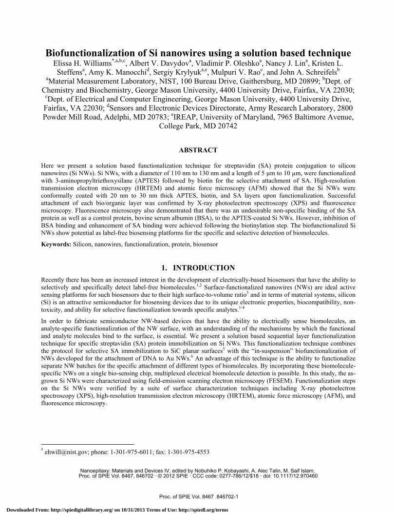
2. EXPERIMENTAL Si NWs were grown in a custom-built chemical vapor deposition (CVD) system described elsewhere.7 Gold nanoparticles (100 nm in diameter) were utilized to facilitate the vapor-liquid-solid (VLS) growth mechanism of the NWs. Figure 1 shows a representative FESEM image of Si NWs grown at 900 °C and 600 Torr using a SiCl4/H2/N2 gas mixture. The vertical orientation of the NWs, with respect to the Si(111) substrate, indicates a <111> NW growth direction. The Si NWs used in this study were 5 µm to 10 µm in length with a diameter of 110 nm to 130 nm.
Figure 1. Tilt-view FESEM image of Si NWs grown on a Si(111) substrate (note solidified gold caps atop the NWs that enabled VLS growth). The NWs were harvested and processed for biofunctionization.
The as-grown Si NWs on the Si(111) substrates were placed in a vial containing a 2% 3-aminopropyltriethoxysilane (APTES) solution in toluene and then sonicated for a few minutes in order to detach the NWs from the substrates and form a suspension. After a 30 min exposure to the APTES solution, the NW suspension was sedimented by centrifugation for 2 min at 10,000 rpm (centrifuge rotor radius is 4 cm) and rinsed with toluene.
To examine the binding of the SA and the bovine serum albumin (BSA) protein to the APTES-coated Si NWs, the APTES functionalized NWs were re-suspended in toluene, placed onto 1 cm × 1 cm clean Si pieces and allowed to air dry. It is important to point out that the Si NWs adhere to the substrate surface by strong electrostatic and van der Waals interactions and are resistant to removal except by excessive sonication. The SA protein was utilized in this study since it is specific for biotin; BSA was used as a control protein for non-specific binding since BSA has no affinity for biotin. The Si substrates with deposited APTES-coated NWs were placed in a mixture of 0.058 mg/mL streptavidin labeled cyanine-3 (SA-cy3) and 0.058 mg/mL bovine serum albumin labeled fluorescein isothiocyanate (BSA-FITC) in 0.01 mol/L phosphate buffer (pH= 7.4) solution for 2 h, rinsed with buffer, and then dried in a N2 flow.
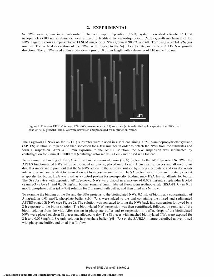
To examine the binding of the SA and the BSA proteins to the biotinylated NWs, 0.5 mL of biotin, at a concentration of 5 mg/mL in 0.01 mol/L phosphate buffer (pH= 7.4), were added to the vial containing the rinsed and sedimented APTES-coated Si NWs (see Figure 2). The solution was sonicated to bring the NWs back into suspension followed by a 2 h exposure to the biotin solution. The biotinylated NW suspension was then centrifuged, followed by removal of the biotin solution from the vial. After rinsing in phosphate buffer and re-suspension in buffer, drops of the biotinylated NWs were placed on clean Si pieces and allowed to dry. The Si pieces with attached biotinylated NWs were exposed for 2 h to a 0.058 mg/mL SA only solution in phosphate buffer (pH= 7.4) or the SA/BSA mixture described above, rinsed with phosphate buffer, and dried in a N2 flow.
Proc. of SPIE Vol. 8467 846702-2
Downloaded From: http://spiedigitallibrary.org/ on 10/31/2013 Terms of Use: http://spiedl.org/terms
NH2
O'H O' O' Si-0 Si Si+ / -111" HO'
I I I OO I O I OH
H H r_
NH2 NH3+ O
HNHi, NH
/H
NW surface )APTES NW surface
Na 0 O
O
17101111
HN'''NH
'DSO
OO HHN ÑH BSABA
VII_ M LI i
HNHi,, NH
iH O
FIN-4Hi./ NH
/H
r 1 nH H
HO" iSi HOSiO/ IOHO p OH O OI 1 I I
NW surface NW surface
S .-,
Figure 2. A schematic demonstrating specific SA binding and the inhibition of BSA binding to biotinylated NWs. Note: the SA and BSA proteins are not drawn to scale.
To examine the binding of SA and BSA to as-grown Si NWs, the as-grown NWs were sonicated off the substrates in a vial containing toluene; the NWs were transferred onto clean Si pieces and then allowed to air dry. The Si pieces containing the as-grown NWs were placed in the SA/BSA mixture described above for 2 h, rinsed with phosphate buffer, and dried under nitrogen.
Oxide formation, APTES functionalization, biotinylation, and protein immobilization on the Si NWs was examined and analyzed using XPS, HRTEM, and AFM. Fluorescence microscopy was utilized on the as-grown, APTES-coated, and biotinylated Si NWs for protein detection and quantification. Instrument details are as follows.
For XPS, the as-grown and functionalized Si NWs were deposited on a Si substrate piece and analyzed in a Kratos Analytical Axis Ultra DLD instrument with a monochromated Al Kα X-ray source at 150 W (10 mA, 15 kV). † X-rays were collected at a 0° angle from the surface normal on an area of 300 µm × 700 µm. Low resolution survey scans (160 eV pass energy, 0.5 eV step size) and high resolution narrow scans (40 eV pass energy, 0.1 eV step size) of O 1s, N 1s, C 1s, Si 2p, and S 2p were obtained. The binding energy scale was calibrated to the C 1s, C*- C aliphatic carbon peak at 285.0 eV. Charge neutralization was not necessary during sample analysis due to the calibration to the aliphatic C 1s peak.
The Si NWs were examined by HRTEM to determine the thickness of the oxide layer and the APTES/biotin/SA layer. The morphology and microstructure of the as-grown and coated Si NWs were characterized on a FEI Titan 80-300 TEM,
† Commercial equipment and material suppliers are identified in this paper to adequately describe experimental procedures. This does not imply endorsement by NIST.
Proc. of SPIE Vol. 8467 846702-3
Downloaded From: http://spiedigitallibrary.org/ on 10/31/2013 Terms of Use: http://spiedl.org/terms
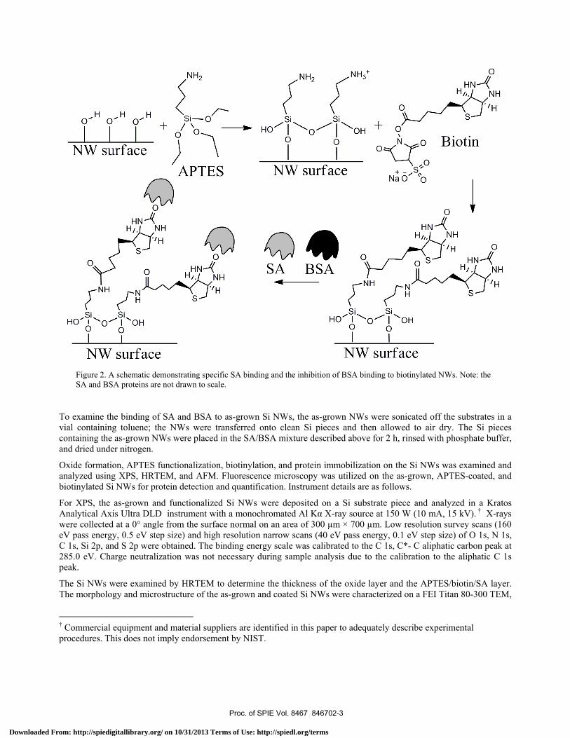
C) Cls
C-O
C-C
I I 1 I I 1 1 1 1 1 1 1 1I I I I I I -1
405 403 401 399 397 167 165 163 161 290 288 286 284
Binding Energy (eV) Binding Energy (eV) Binding Energy (eV)
equipped with S-TWIN objective lenses, at a 300 kV accelerating voltage. Low intensity illumination conditions and beam blanking were used to minimize possible radiation damage of the samples.
The surface topography and morphology of the as-grown and functionalized Si NWs were investigated with a Veeco DI DimensionV AFM on a 1 µm × 1 µm scale in tapping mode. Images were analyzed using the WSxM v5.0 software.8
Fluorescence microscopy of the protein conjugated as-grown, APTES-coated, and biotinylated Si NWs was performed using a Nikon Eclipse TE300 inverted epifluorescence microscope with a Plan Apo 60X (N.A. 1.4) oil immersion objective. SA-cy3 was imaged using a Nikon EF.4 filter cube with an excitation of 515 nm to 565 nm at a 1 s exposure time. BSA-FITC was imaged using the Nikon B-2E/C filter cube with an excitation of 465 nm to 495 nm at a 9 s exposure time; the relatively long exposure time of 9 s was necessary to enhance the weak fluorescence signal of BSA.
3. RESULTS AND DISCUSSION 3.1 X-ray photoelectron spectroscopy (XPS)
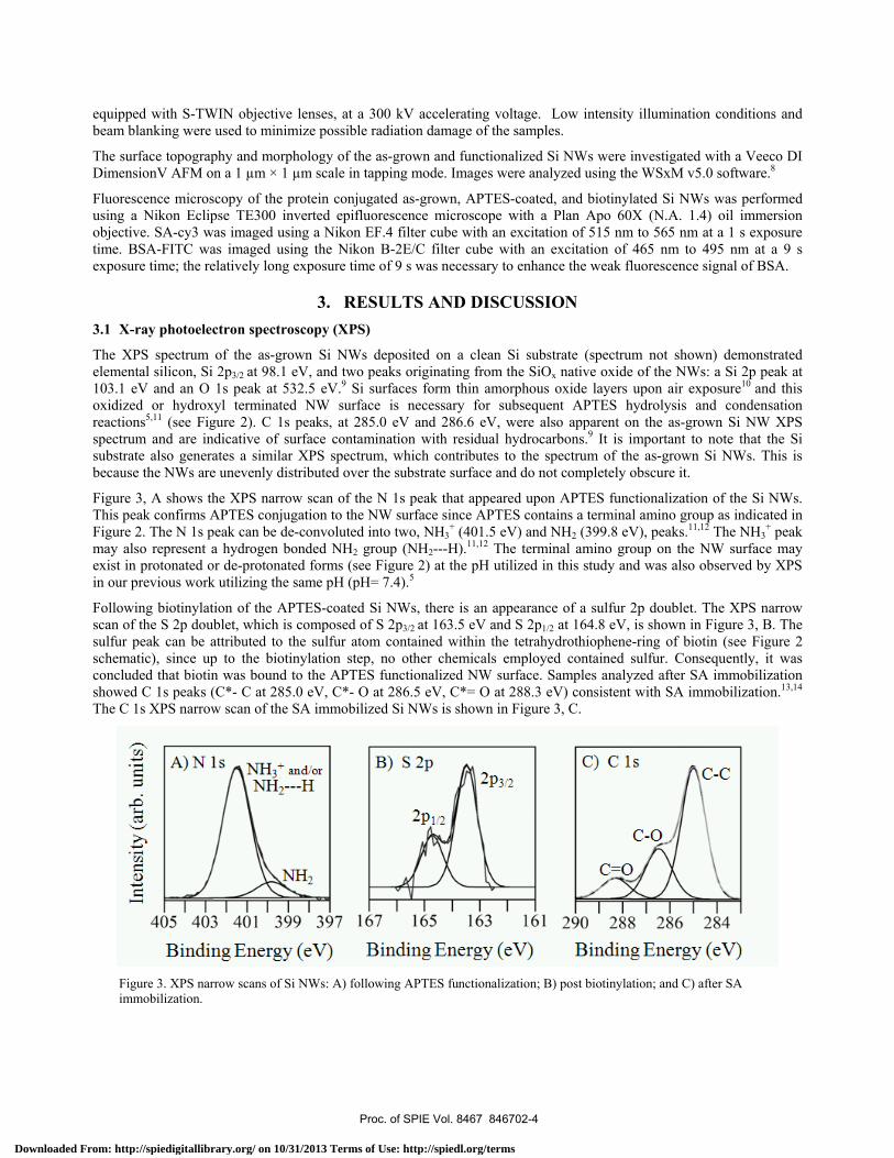
The XPS spectrum of the as-grown Si NWs deposited on a clean Si substrate (spectrum not shown) demonstrated elemental silicon, Si 2p3/2 at 98.1 eV, and two peaks originating from the SiOx native oxide of the NWs: a Si 2p peak at 103.1 eV and an O 1s peak at 532.5 eV.9 Si surfaces form thin amorphous oxide layers upon air exposure10 and this oxidized or hydroxyl terminated NW surface is necessary for subsequent APTES hydrolysis and condensation reactions5,11 (see Figure 2). C 1s peaks, at 285.0 eV and 286.6 eV, were also apparent on the as-grown Si NW XPS spectrum and are indicative of surface contamination with residual hydrocarbons.9 It is important to note that the Si substrate also generates a similar XPS spectrum, which contributes to the spectrum of the as-grown Si NWs. This is because the NWs are unevenly distributed over the substrate surface and do not completely obscure it.
Figure 3, A shows the XPS narrow scan of the N 1s peak that appeared upon APTES functionalization of the Si NWs. This peak confirms APTES conjugation to the NW surface since APTES contains a terminal amino group as indicated in Figure 2. The N 1s peak can be de-convoluted into two, NH3
+ (401.5 eV) and NH2 (399.8 eV), peaks.11,12 The NH3+ peak
may also represent a hydrogen bonded NH2 group (NH2---H).11,12 The terminal amino group on the NW surface may exist in protonated or de-protonated forms (see Figure 2) at the pH utilized in this study and was also observed by XPS in our previous work utilizing the same pH (pH= 7.4).5
Following biotinylation of the APTES-coated Si NWs, there is an appearance of a sulfur 2p doublet. The XPS narrow scan of the S 2p doublet, which is composed of S 2p3/2 at 163.5 eV and S 2p1/2 at 164.8 eV, is shown in Figure 3, B. The sulfur peak can be attributed to the sulfur atom contained within the tetrahydrothiophene-ring of biotin (see Figure 2 schematic), since up to the biotinylation step, no other chemicals employed contained sulfur. Consequently, it was concluded that biotin was bound to the APTES functionalized NW surface. Samples analyzed after SA immobilization showed C 1s peaks (C*- C at 285.0 eV, C*- O at 286.5 eV, C*= O at 288.3 eV) consistent with SA immobilization.13,14
The C 1s XPS narrow scan of the SA immobilized Si NWs is shown in Figure 3, C.
Figure 3. XPS narrow scans of Si NWs: A) following APTES functionalization; B) post biotinylation; and C) after SA immobilization.
Proc. of SPIE Vol. 8467 846702-4
Downloaded From: http://spiedigitallibrary.org/ on 10/31/2013 Terms of Use: http://spiedl.org/terms
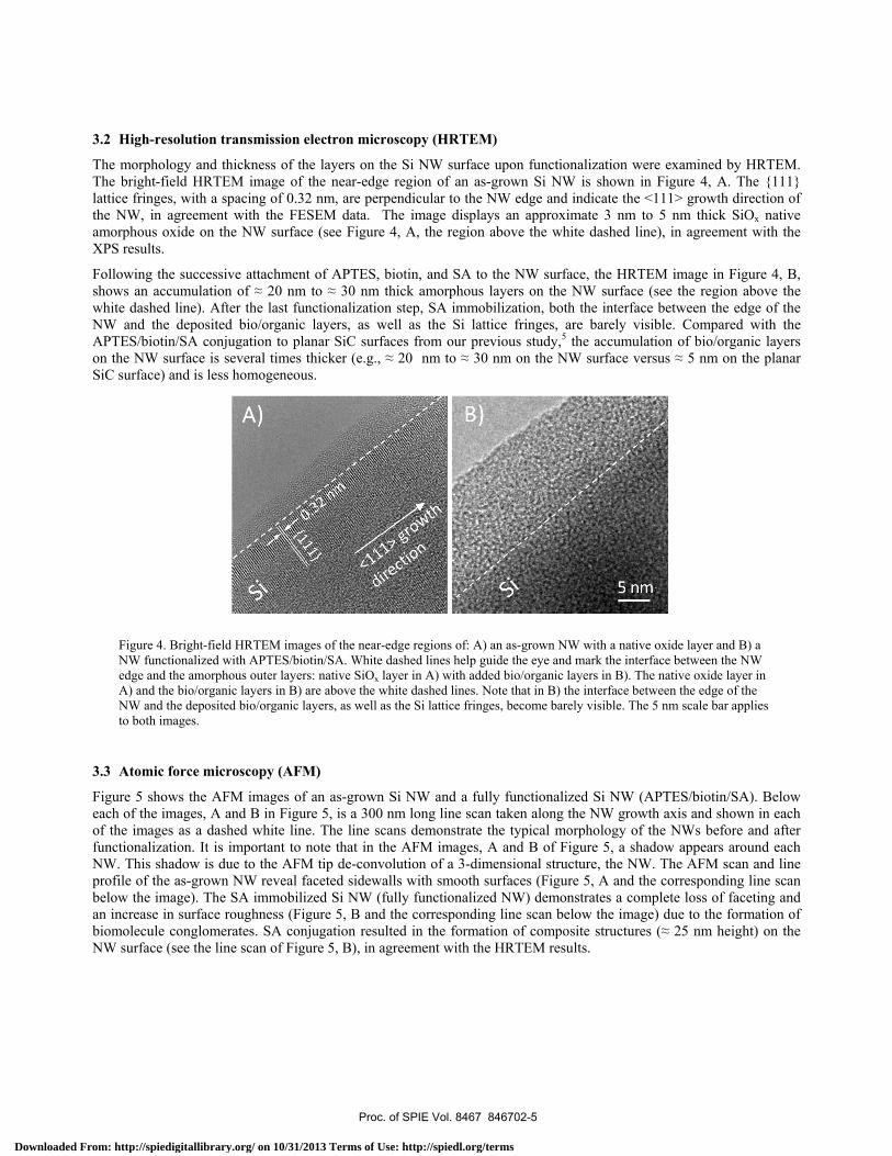
3.2 High-resolution transmission electron microscopy (HRTEM)
The morphology and thickness of the layers on the Si NW surface upon functionalization were examined by HRTEM. The bright-field HRTEM image of the near-edge region of an as-grown Si NW is shown in Figure 4, A. The {111} lattice fringes, with a spacing of 0.32 nm, are perpendicular to the NW edge and indicate the <111> growth direction of the NW, in agreement with the FESEM data. The image displays an approximate 3 nm to 5 nm thick SiOx native amorphous oxide on the NW surface (see Figure 4, A, the region above the white dashed line), in agreement with the XPS results.
Following the successive attachment of APTES, biotin, and SA to the NW surface, the HRTEM image in Figure 4, B, shows an accumulation of ≈ 20 nm to ≈ 30 nm thick amorphous layers on the NW surface (see the region above the white dashed line). After the last functionalization step, SA immobilization, both the interface between the edge of the NW and the deposited bio/organic layers, as well as the Si lattice fringes, are barely visible. Compared with the APTES/biotin/SA conjugation to planar SiC surfaces from our previous study,5 the accumulation of bio/organic layers on the NW surface is several times thicker (e.g., ≈ 20 nm to ≈ 30 nm on the NW surface versus ≈ 5 nm on the planar SiC surface) and is less homogeneous.
Figure 4. Bright-field HRTEM images of the near-edge regions of: A) an as-grown NW with a native oxide layer and B) a NW functionalized with APTES/biotin/SA. White dashed lines help guide the eye and mark the interface between the NW edge and the amorphous outer layers: native SiOx layer in A) with added bio/organic layers in B). The native oxide layer in A) and the bio/organic layers in B) are above the white dashed lines. Note that in B) the interface between the edge of the NW and the deposited bio/organic layers, as well as the Si lattice fringes, become barely visible. The 5 nm scale bar applies to both images.
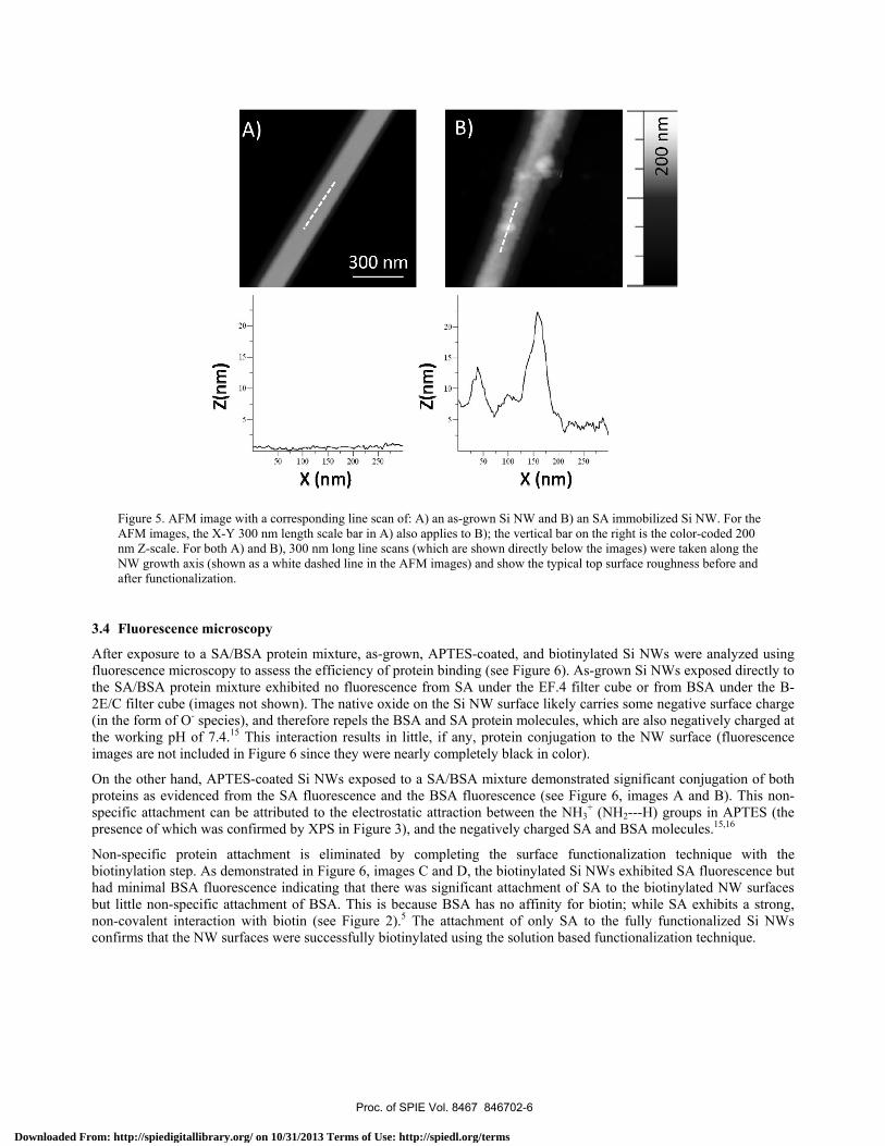
3.3 Atomic force microscopy (AFM)
Figure 5 shows the AFM images of an as-grown Si NW and a fully functionalized Si NW (APTES/biotin/SA). Below each of the images, A and B in Figure 5, is a 300 nm long line scan taken along the NW growth axis and shown in each of the images as a dashed white line. The line scans demonstrate the typical morphology of the NWs before and after functionalization. It is important to note that in the AFM images, A and B of Figure 5, a shadow appears around each NW. This shadow is due to the AFM tip de-convolution of a 3-dimensional structure, the NW. The AFM scan and line profile of the as-grown NW reveal faceted sidewalls with smooth surfaces (Figure 5, A and the corresponding line scan below the image). The SA immobilized Si NW (fully functionalized NW) demonstrates a complete loss of faceting and an increase in surface roughness (Figure 5, B and the corresponding line scan below the image) due to the formation of biomolecule conglomerates. SA conjugation resulted in the formation of composite structures (≈ 25 nm height) on the NW surface (see the line scan of Figure 5, B), in agreement with the HRTEM results.
Proc. of SPIE Vol. 8467 846702-5
Downloaded From: http://spiedigitallibrary.org/ on 10/31/2013 Terms of Use: http://spiedl.org/terms
rI
50 100 150 200 250 50 100 150 200 250
Figure 5. AFM image with a corresponding line scan of: A) an as-grown Si NW and B) an SA immobilized Si NW. For the AFM images, the X-Y 300 nm length scale bar in A) also applies to B); the vertical bar on the right is the color-coded 200 nm Z-scale. For both A) and B), 300 nm long line scans (which are shown directly below the images) were taken along the NW growth axis (shown as a white dashed line in the AFM images) and show the typical top surface roughness before and after functionalization.
3.4 Fluorescence microscopy
After exposure to a SA/BSA protein mixture, as-grown, APTES-coated, and biotinylated Si NWs were analyzed using fluorescence microscopy to assess the efficiency of protein binding (see Figure 6). As-grown Si NWs exposed directly to the SA/BSA protein mixture exhibited no fluorescence from SA under the EF.4 filter cube or from BSA under the B-2E/C filter cube (images not shown). The native oxide on the Si NW surface likely carries some negative surface charge (in the form of O- species), and therefore repels the BSA and SA protein molecules, which are also negatively charged at the working pH of 7.4.15 This interaction results in little, if any, protein conjugation to the NW surface (fluorescence images are not included in Figure 6 since they were nearly completely black in color).
On the other hand, APTES-coated Si NWs exposed to a SA/BSA mixture demonstrated significant conjugation of both proteins as evidenced from the SA fluorescence and the BSA fluorescence (see Figure 6, images A and B). This non-specific attachment can be attributed to the electrostatic attraction between the NH3
+ (NH2---H) groups in APTES (the presence of which was confirmed by XPS in Figure 3), and the negatively charged SA and BSA molecules.15,16
Non-specific protein attachment is eliminated by completing the surface functionalization technique with the biotinylation step. As demonstrated in Figure 6, images C and D, the biotinylated Si NWs exhibited SA fluorescence but had minimal BSA fluorescence indicating that there was significant attachment of SA to the biotinylated NW surfaces but little non-specific attachment of BSA. This is because BSA has no affinity for biotin; while SA exhibits a strong, non-covalent interaction with biotin (see Figure 2).5 The attachment of only SA to the fully functionalized Si NWs confirms that the NW surfaces were successfully biotinylated using the solution based functionalization technique.
Proc. of SPIE Vol. 8467 846702-6
Downloaded From: http://spiedigitallibrary.org/ on 10/31/2013 Terms of Use: http://spiedl.org/terms
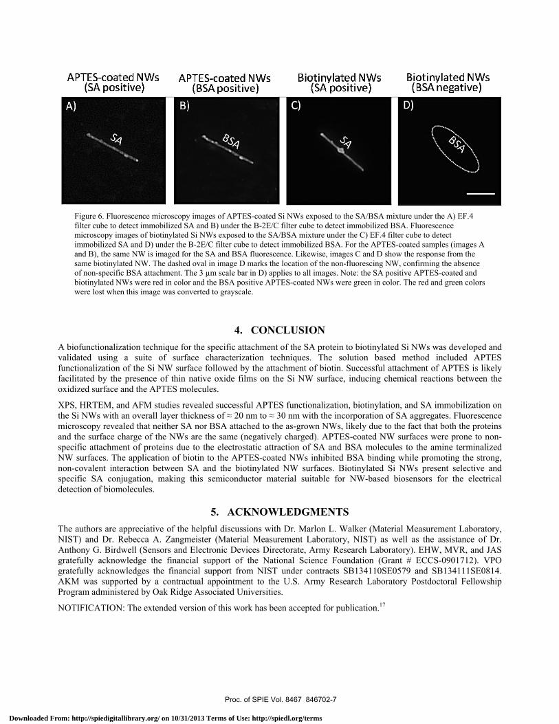
Figure 6. Fluorescence microscopy images of APTES-coated Si NWs exposed to the SA/BSA mixture under the A) EF.4 filter cube to detect immobilized SA and B) under the B-2E/C filter cube to detect immobilized BSA. Fluorescence microscopy images of biotinylated Si NWs exposed to the SA/BSA mixture under the C) EF.4 filter cube to detect immobilized SA and D) under the B-2E/C filter cube to detect immobilized BSA. For the APTES-coated samples (images A and B), the same NW is imaged for the SA and BSA fluorescence. Likewise, images C and D show the response from the same biotinylated NW. The dashed oval in image D marks the location of the non-fluorescing NW, confirming the absence of non-specific BSA attachment. The 3 µm scale bar in D) applies to all images. Note: the SA positive APTES-coated and biotinylated NWs were red in color and the BSA positive APTES-coated NWs were green in color. The red and green colors were lost when this image was converted to grayscale.
4. CONCLUSION A biofunctionalization technique for the specific attachment of the SA protein to biotinylated Si NWs was developed and validated using a suite of surface characterization techniques. The solution based method included APTES functionalization of the Si NW surface followed by the attachment of biotin. Successful attachment of APTES is likely facilitated by the presence of thin native oxide films on the Si NW surface, inducing chemical reactions between the oxidized surface and the APTES molecules.
XPS, HRTEM, and AFM studies revealed successful APTES functionalization, biotinylation, and SA immobilization on the Si NWs with an overall layer thickness of ≈ 20 nm to ≈ 30 nm with the incorporation of SA aggregates. Fluorescence microscopy revealed that neither SA nor BSA attached to the as-grown NWs, likely due to the fact that both the proteins and the surface charge of the NWs are the same (negatively charged). APTES-coated NW surfaces were prone to non-specific attachment of proteins due to the electrostatic attraction of SA and BSA molecules to the amine terminalized NW surfaces. The application of biotin to the APTES-coated NWs inhibited BSA binding while promoting the strong, non-covalent interaction between SA and the biotinylated NW surfaces. Biotinylated Si NWs present selective and specific SA conjugation, making this semiconductor material suitable for NW-based biosensors for the electrical detection of biomolecules.
5. ACKNOWLEDGMENTS The authors are appreciative of the helpful discussions with Dr. Marlon L. Walker (Material Measurement Laboratory, NIST) and Dr. Rebecca A. Zangmeister (Material Measurement Laboratory, NIST) as well as the assistance of Dr. Anthony G. Birdwell (Sensors and Electronic Devices Directorate, Army Research Laboratory). EHW, MVR, and JAS gratefully acknowledge the financial support of the National Science Foundation (Grant # ECCS-0901712). VPO gratefully acknowledges the financial support from NIST under contracts SB134110SE0579 and SB134111SE0814. AKM was supported by a contractual appointment to the U.S. Army Research Laboratory Postdoctoral Fellowship Program administered by Oak Ridge Associated Universities.
NOTIFICATION: The extended version of this work has been accepted for publication.17
Proc. of SPIE Vol. 8467 846702-7
Downloaded From: http://spiedigitallibrary.org/ on 10/31/2013 Terms of Use: http://spiedl.org/terms
REFERENCES
[1] Patolsky, F., Zheng, G., and Lieber, C.M., “Fabrication of silicon nanowire devices for ultrasensitive, label-free, real-time detection of biological and chemical species,” Nat. Protoc. 1(4), 1711-1724 (2006).
[2] Patolsky, F., Zheng, G., and Lieber, C.M., “Nanowire-based biosensors,” Anal. Chem. 78(13), 4261-4269 (2006). [3] Guo, D.J., Abdulagatov, A.I., Rourke, D.M., Bertness, K.A., George, S.M., Lee, Y.C., and Tan, W., “GaN nanowire
functionalized with atomic layer deposition techniques for enhanced immobilization of biomolecules,” Langmuir 26(23), 18382-18391 (2010).
[4] Shao, M., Ma, D.D.D., and Lee, S-T., “Silicon nanowires- synthesis, properties, and applications,” Eur. J. Inorg. Chem. 27, 4264-4278 (2010).
[5] Williams, E.H., Davydov, A.V., Motayed, A., Sundaresan, S.G., Bocchini, P., Richter, L.J., Stan, G., Steffens, K., Zangmeister, R., Schreifels, J.A., and Rao, M.V., “Immobilization of streptavidin on 4H-SiC for biosensor development,” Appl. Surf. Sci. 16, 6056-6063 (2012).
[6] Sioss, J.A., Stoermer, R.L., Sha, M.Y., and Keating, C.D., “Silica-coated, Au/Ag striped nanowires for bioanalysis,” Langmuir 23, 11334-11341 (2007).
[7] Krylyuk, S., Davydov, A.V., and Levin, I., “Tapering control of Si nanowires grown from SiCl4 at reduced pressure,” ACS Nano 5(1), 656-664 (2011).
[8] Horcas, I., Fernández, R., Gómez-Rodriguez, G.M., Colchero, J., Gómez-Herrero, J., and Baro, A.M., “WSxM: a software for scanning probe microscopy and a tool for nanotechnology,” Rev. Sci. Instrum. 78(1), 013705-8 (2007).
[9] Wagner, C.D., Naumkin, A.V., Kraut-Vass, A., Allison, J.W., Powell, C.J., and Rumble, J.R., “NIST x-ray photoelectron spectroscopy database,” version 3.5, http://srdata.nist.gov/xps/Default.aspx (2007).
[10] Morita, M., Ohmi, T., Hasegawa, E., Kawakami, M., and Ohwada, M., “Growth of native oxide on a silicon surface,” J. Appl. Phys. 68(3), 1272-1282 (1990).
[11] Arranz, A., Palacio, C., Garcia-Fresnadillo, D., Orellana, G., Navarro, A., and Muñoz, E., “Influence of surface hydroxylation on 3-aminopropyltriethoxysilane growth mode during chemical functionalization of GaN surfaces: an angle-resolved x-ray photoelectron spectroscopy study,” Langmuir 24, 8667-8671 (2008).
[12] Vandenberg, E.T., Bertilsson, L., Liedberg, B., Uvdal, K., Erlandsson, R., Elwing, H., and Lundström, I., “Structure of 3-aminopropyltriethoxysilane on silicon oxide,” J. Colloid Interface Sci. 147(1), 103-118 (1991).
[13] Ruiz-Taylor, L.A., Martin, T.L., Zaugg, F.G., Witte, K., Indermuhle, P., Nock, S., and Wagner, P., “Monolayers of derivatized poly(L-lysine)-grafted-poly(ethylene glycol) on metal oxides as a class of biomolecular interfaces,” Proc. Natl. Acad. Sci. U.S.A. 98(3) 852-857 (2001).
[14] Yang, Z., Xie, Z., Liu, H., Yan, F., and Ju, H., “Streptavidin-functionalized three-dimensional ordered nanoporous silica film for highly efficient chemiluminescent immunosensing,” Adv. Funct. Mater. 18(24) 3991-3998 (2008).
[15] Righetti, P.G., and Tudor, G., “Isoelectric points and molecular weights of proteins: a new table,” J. Chromatogr. A 220(2), 115-194 (1981).
[16] Wang, Y., Qian, W., Tan, Y., and Ding, S., “A label-free biosensor based on gold nanoshell monolayers for monitoring biomolecular interactions in diluted whole blood,” Biosens. Bioelectron. 23(7), 1166-1170 (2008).
[17] Williams, E.H., Schreifels, J.A., Rao, M.V., Davydov, A.V., Oleshko, V.P., Lin, N.J., Steffens, K.L., Krylyuk, S., Bertness, K., Manocchi, A., Koshka, Y., “Selective streptavidin bioconjugation on Si and SiC nanowires for biosensor applications,” J. Mater. Res., accepted for publication (2012).
Proc. of SPIE Vol. 8467 846702-8
Downloaded From: http://spiedigitallibrary.org/ on 10/31/2013 Terms of Use: http://spiedl.org/terms


