Embed Size (px)
Citation preview
International Journal on Organic Electronics (IJOE) Vol.3, No.1/2/3/4, October 2014
DOI: 10.5121/ijoe.2014.3401 1
FABRICATION AND CHARACTERIZATION OF NICKEL
NANOWIRES
Raminder Kaur
Department of Basic and Applied Sciences, Punjabi University, Patiala, India
ABSTRACT
This paper shows that nickel nanowires of length 11µm and diameters 800 and 15nm were grown within
the pores of nuclear track polycarbonate membrane by electrodepositing nickel. Surface morphology and
crystallographic structure of the deposited nanowires was investigated using SEM, TEM and XRD
respectively. It is found that low current density gives good result, while high current density leads to the
formation of curled nanowires. Fabricated nanowires were further investigated for electrical properties
and found that nanowires obey ohm’s law. Through structural characterization it has been observed that
the fabricated nanowires posses FCC lattice structure.
KEYWORDS
Nanowires, nuclear track membrane, electrodeposition
1. INTRODUCTION
Nanowires are one of the most interesting nanostructures with potential application in the field of sensors and renewable energy devices. Out of the various fabrication techniques, such as self-assembly [1], sputtering or evaporation, template-based synthesis is the most suitable one for fabricating metallic nanowires. Template synthesis [2] is relatively inexpensive and simple technique, through which the nanowires can be formed in a uniform and parallel porous structure. In template synthesis process, size and shape of the nanowires remain confined to the pores of template. A versatile approach that has been used by a number of groups for fabricating freestanding metal, semiconductors and polymers nanowires through electrodeposition into nanoporous membrane template was given by Possin [3] and C. R. Martin [1]. A technique suitable for fabricating structure with high aspect ratios and small lateral dimensions involves a combination of heavy ion irradiation and chemical etching of some dielectric materials [4]. Conditions related to electrolyte composition and electroplating parameters, such as current density, electrolyte temperature etc. markedly affect the properties and structure of Ni nanowires [5]. Metal nanowires are of great interest due to their electrical [6,7], optical [8,9] and magnetic [10] properties. 2. FABRICATION AND CHARACTERIZATION
In the present work, the technique of template synthesis has been employed for fabricating high aspect-ratio nanowires of nickel into the pores of nuclepore polycarbonate membranes having nominal pore size of 800 and 15nm, with a pore density of 108 cm–2 and 11 µm thicknesses. Two-electrode electrochemical cell has been used for depositing nickel into the pores of the template. Similar cell design has been used previously for fabricating copper nanowires [11].
International Journal on Organic Electronics (IJOE) Vol.3, No.1/2/3/4, October 2014
2
Nickel plating is similar to other electroplating processes that employ soluble metal anodes. It requires the passage of direct current between two electrodes that are immersed in a conductive, aqueous solution of nickel salt. The flow of direct current causes one of the electrodes (the anode) to dissolve and the other electrode (cathode) to get covered with a layer of elemental nickel. For deposition of nickel nanowires, the cell was filled with freshly prepared and filtered electrolyte, comprising of 60 g/l of NiSO4.6H2O along with 30 g/l of H3BO3 (Boric Acid) dissolved in double distilled, de-ionized water at room temperature (35°C). Nickel sulfate is available in commercially pure form and is relatively inexpensive. Boric acid is used for buffering purposes. The electrodeposition was performed potentiostatically at a low current density of 6 mA/cm2
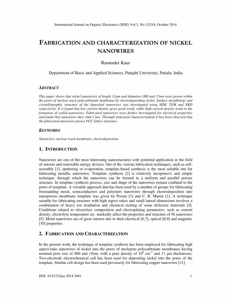
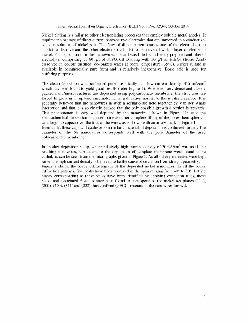
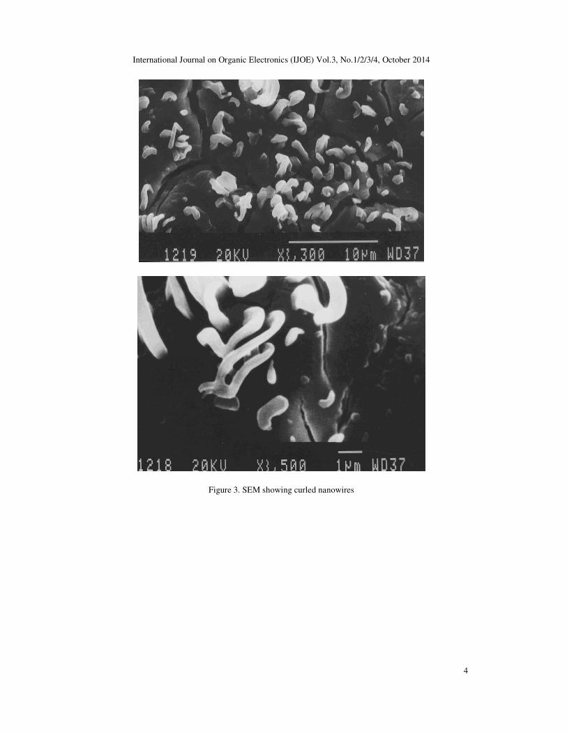
which has been found to yield good results (refer Figure 1). Whenever very dense and closely packed nano/microstructures are deposited using polycarbonate membrane, the structures are forced to grow in an upward ensemble, i.e. in a direction normal to the substrate surface. It is generally believed that the nanowires in such a scenario are held together by Van der Waals interaction and that it is so closely packed that the only possible growth direction is upwards. This phenomenon is very well depicted by the nanowires shown in Figure 1In case the electrochemical deposition is carried out even after complete filling of the pores, hemispherical caps begin to appear over the tops of the wires, as is shown with an arrow-mark in Figure 1 Eventually, these caps will coalesce to form bulk material, if deposition is continued further. The diameter of the Ni nanoowires corresponds well with the pore diameter of the used polycarbonate membrane. In another deposition setup, where relatively high current density of 30mA/cm2 was used, the resulting nanowires, subsequent to the deposition of template membrane were found to be curled, as can be seen from the micrographs given in Figure 3. As all other parameters were kept same, the high current density is believed to be the cause of deviation from straight geometry. Figure 2 shows the X-ray diffractogram of the deposited nickel nanowires. In all the X-ray diffraction patterns, five peaks have been observed in the span ranging from 40° to 80°. Lattice planes corresponding to these peaks have been identified by applying extinction rules, these peaks and associated d-values have been found to correspond to the nickel hkl planes (111), (200), (220), (311) and (222) thus confirming FCC structure of the nanowires formed.
International Journal on Organic Electronics (IJOE) Vol.3, No.1/2/3/4, October 2014
3
Figure 1. SEM image showing nickel nanowires grown in membrane having pore diameter of 800nm
Figure 2. X-Ray diffractogram of nickel nanowires deposited at 40ºC in membrane having pore diameter of 800nm.
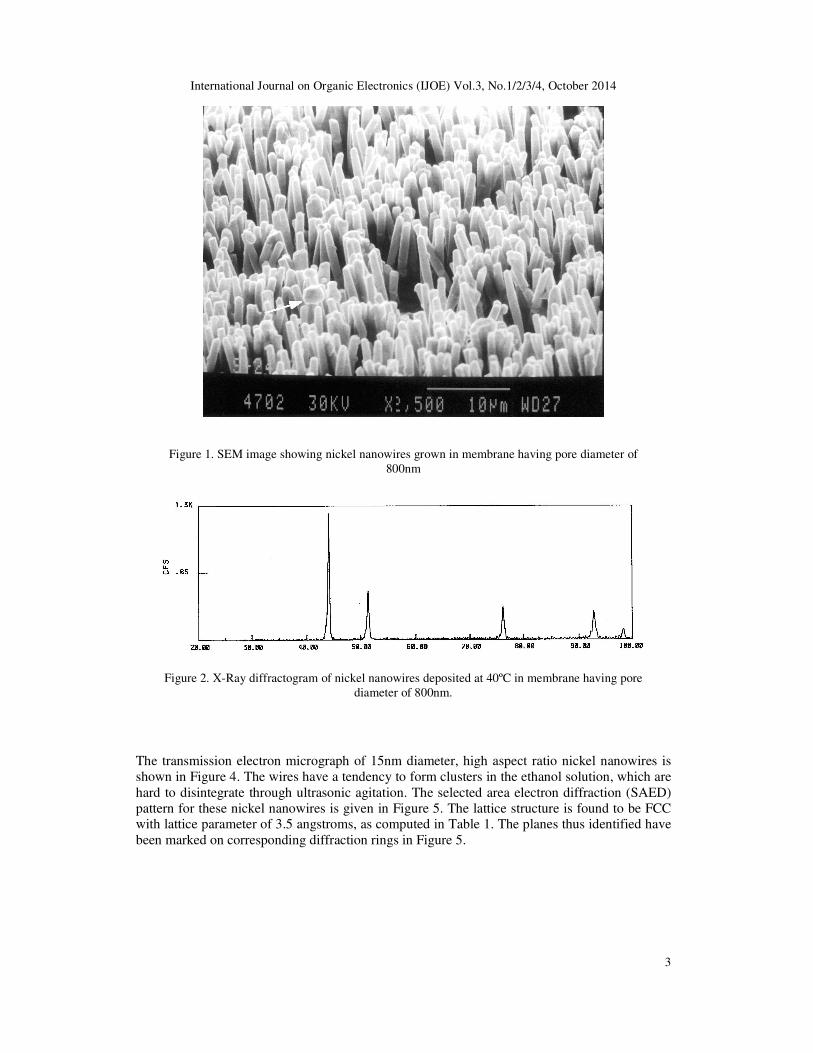
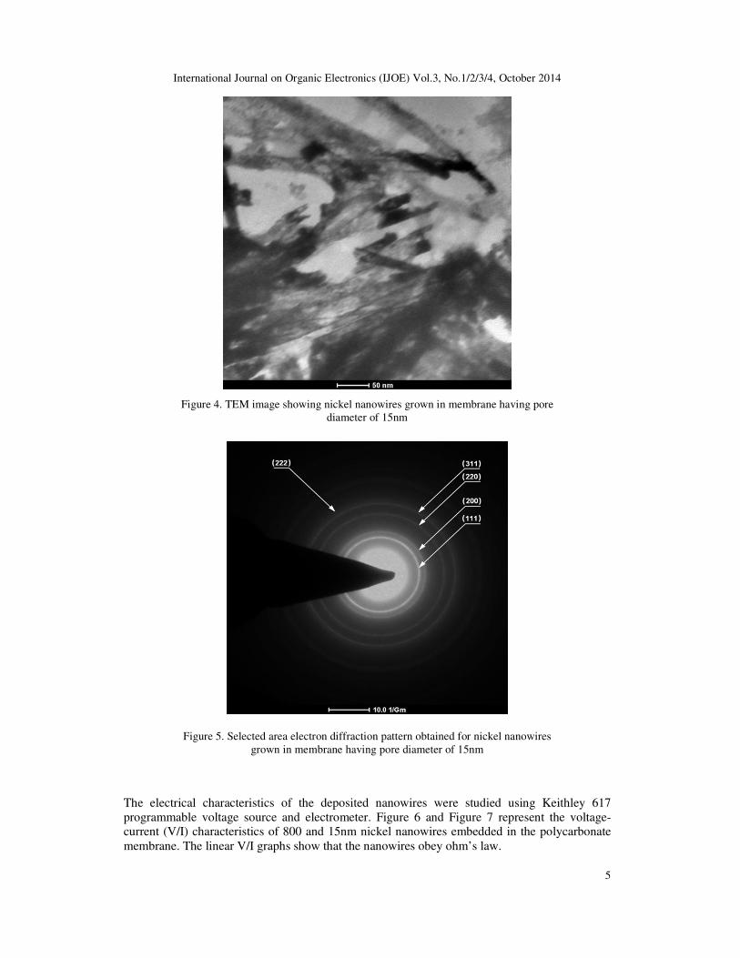
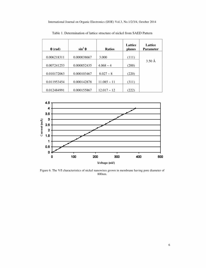
The transmission electron micrograph of 15nm diameter, high aspect ratio nickel nanowires is shown in Figure 4. The wires have a tendency to form clusters in the ethanol solution, which are hard to disintegrate through ultrasonic agitation. The selected area electron diffraction (SAED) pattern for these nickel nanowires is given in Figure 5. The lattice structure is found to be FCC with lattice parameter of 3.5 angstroms, as computed in Table 1. The planes thus identified have been marked on corresponding diffraction rings in Figure 5.
International Journal on Organic Electronics (IJOE) Vol.3, No.1/2/3/4, October 2014
4
Figure 3. SEM showing curled nanowires
International Journal on Organic Electronics (IJOE) Vol.3, No.1/2/3/4, October 2014
5
Figure 4. TEM image showing nickel nanowires grown in membrane having pore
diameter of 15nm
Figure 5. Selected area electron diffraction pattern obtained for nickel nanowires grown in membrane having pore diameter of 15nm
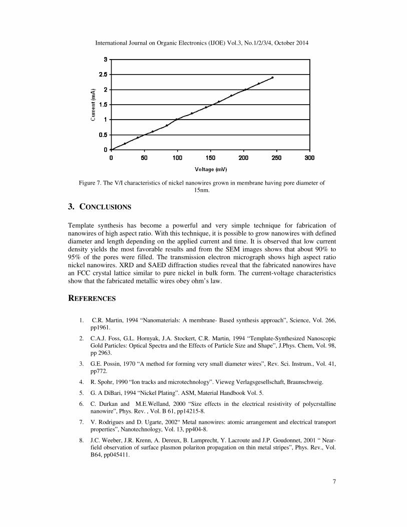
The electrical characteristics of the deposited nanowires were studied using Keithley 617 programmable voltage source and electrometer. Figure 6 and Figure 7 represent the voltage-current (V/I) characteristics of 800 and 15nm nickel nanowires embedded in the polycarbonate membrane. The linear V/I graphs show that the nanowires obey ohm’s law.
International Journal on Organic Electronics (IJOE) Vol.3, No.1/2/3/4, October 2014
6
Table 1. Determination of lattice structure of nickel from SAED Pattern
θθθθ (rad) sin2 θθθθ Ratios
Lattice
planes
Lattice
Parameter
0.006218311
0.000038667
3.000
(111)
3.50 Å 0.007241253
0.000052435
4.068 ~ 4
(200)
0.010172063
0.000103467
8.027 ~ 8
(220)
0.011953454
0.000142878
11.085 ~ 11
(311)
0.012484991
0.000155867
12.017 ~ 12
(222)
Figure 6. The V/I characteristics of nickel nanowires grown in membrane having pore diameter of
800nm.
International Journal on Organic Electronics (IJOE) Vol.3, No.1/2/3/4, October 2014
7
Figure 7. The V/I characteristics of nickel nanowires grown in membrane having pore diameter of
15nm.
3. CONCLUSIONS
Template synthesis has become a powerful and very simple technique for fabrication of nanowires of high aspect ratio. With this technique, it is possible to grow nanowires with defined diameter and length depending on the applied current and time. It is observed that low current density yields the most favorable results and from the SEM images shows that about 90% to 95% of the pores were filled. The transmission electron micrograph shows high aspect ratio nickel nanowires. XRD and SAED diffraction studies reveal that the fabricated nanowires have an FCC crystal lattice similar to pure nickel in bulk form. The current-voltage characteristics show that the fabricated metallic wires obey ohm’s law.
REFERENCES
1. C.R. Martin, 1994 “Nanomaterials: A membrane- Based synthesis approach”, Science, Vol. 266, pp1961.
2. C.A.J. Foss, G.L. Hornyak, J.A. Stockert, C.R. Martin, 1994 “Template-Synthesized Nanoscopic Gold Particles: Optical Spectra and the Effects of Particle Size and Shape”, J.Phys. Chem, Vol. 98, pp 2963.
3. G.E. Possin, 1970 “A method for forming very small diameter wires”, Rev. Sci. Instrum., Vol. 41, pp772.
4. R. Spohr, 1990 “Ion tracks and microtechnology”. Vieweg Verlagsgesellschaft, Braunschweig.
5. G. A DiBari, 1994 “Nickel Plating”. ASM, Material Handbook Vol. 5.
6. C. Durkan and M.E.Welland, 2000 “Size effects in the electrical resistivity of polycrstalline nanowire”, Phys. Rev. , Vol. B 61, pp14215-8.
7. V. Rodrigues and D. Ugarte, 2002“ Metal nanowires: atomic arrangement and electrical transport properties”, Nanotechnology, Vol. 13, pp404-8.
8. J.C. Weeber, J.R. Krenn, A. Dereux, B. Lamprecht, Y. Lacroute and J.P. Goudonnet, 2001 “ Near-field observation of surface plasmon polariton propagation on thin metal stripes”, Phys. Rev., Vol. B64, pp045411.
International Journal on Organic Electronics (IJOE) Vol.3, No.1/2/3/4, October 2014
8
9. G. Schider, J.R. Krenn, W. Gotschy, B. Lamprecht, H. Ditlbacher, a. Leitner and F.R. Aussenegg, 2001“ Optical properties of Ag and Au nanowires gratings ”, J. Appl. Phys., Vol. 90, pp 3825-30.
10. D. J. Sellmyer, M. Zheng and R. Skomski,2001“Magnetism of Fe, Co and Ni nanowires in self-assembled arrays”, J. Phys. Condens. Matter, Vol.13, pp R433-60.
11. R. Kaur, N. K Vema, S.K Chakarvarti, S. Kumar, 2006 “Fabrication of copper microcylinders in polycarbonate membranes and their characterization” J Mater Sci., pp 41:3723.
Author
Dr. Raminder Kaur is presently working as Assistant Professor in the Department of Basic and Applied Sciences, Punjabi University, Patiala, Punjab, India. She has been pursuing research on fabrication, characterization and application of nanomaterials since 2003.


