Embed Size (px)
Citation preview

sensors
Technical Note
Fault Injection Emulation for Systems in FPGAs: Tools,Techniques and Methodology, a Tutorial
Óscar Ruano , Francisco García-Herrero * , Luis Alberto Aranda , Alfonso Sánchez-Macián ,Laura Rodriguez and Juan Antonio Maestro
�����������������
Citation: Ruano, Ó.; García-Herrero,
F.; Aranda, L.A.; Sánchez-Macián, A.;
Rodriguez, L.; Maestro, J.A. Fault
Injection Emulation for Systems in
FPGAs: Tools, Techniques and
Methodology, a Tutorial. Sensors 2021,
21, 1392. https://doi.org/10.3390/
s21041392
Academic Editor: Mario Marchese
Received: 25 January 2021
Accepted: 12 February 2021
Published: 17 February 2021
Publisher’s Note: MDPI stays neutral
with regard to jurisdictional claims in
published maps and institutional affil-
iations.
Copyright: © 2021 by the authors.
Licensee MDPI, Basel, Switzerland.
This article is an open access article
distributed under the terms and
conditions of the Creative Commons
Attribution (CC BY) license (https://
creativecommons.org/licenses/by/
4.0/).
ARIES Research Center, Universidad Antonio Nebrija, 28040 Madrid, Spain; [email protected] (Ó.R.);[email protected] (L.A.A.); [email protected] (A.S.-M.); [email protected] (L.R.);[email protected] (J.A.M.)* Correspondence: [email protected]
Abstract: Communication systems that work in jeopardized environments such as space are affectedby soft errors that can cause malfunctions in the behavior of the circuits such as, for example, singleevent upsets (SEUs) or multiple bit upsets (MBUs). In order to avoid this erroneous functioning,this kind of systems are usually protected using redundant logic such as triple modular redundancy(TMR) or error correction codes (ECCs). After the implementation of the protected modules, thecommunication modules must be tested to assess the achieved reliability. These tests could bedriven into accelerator facilities through ionization processes or they can be performed using faultinjection tools based on software simulation such as the SEUs simulation tool (SST), or based onfield-programmable gate array (FPGA) emulation like the one described in this work. In this paper, atutorial for the setup of a fault injection emulation platform based on the Xilinx soft error mitigation(SEM) intellectual property (IP) controller is depicted step by step, showing a complete cycle. Toillustrate this procedure, an online repository with a complete project and a step-by-step guide isprovided, using as device under test a classical communication component such as a finite impulseresponse (FIR) filter. Finally, the integration of the automatic configuration memory error-injection(ACME) tool to speed up the fault injection process is explained in detail at the end of the paper.
Keywords: communication modules; emulation; fault injection debugger; FIR filter; SEM IP; SEU; Xil-inx
1. Introduction
The reliability feature for communication systems that must work in harsh environ-ments such as space or radioactively contaminated areas, is a major concern nowadays [1,2].For these scenarios, not only area, delay and power consumption play an important role inthe design process, but also fault tolerance is mandatory in order to deal with soft errorssuch as single event upsets (SEUs), multiple bit upsets (MBUs) or single event functionalinterrupt (SEFIs) produced by radiation [3]. These upsets are caused by ionizing radiationstrikes that alter the charge in storage elements such as configuration memory cells, usermemory or registers, causing non-permanent errors in the systems. In order to avoid theseerrors, there are two main approaches.
The first option called radiation-hardening by process (RHBP), includes physicaltechniques that must change the manufacturing process by means of shielding or applyingsilicon on insulator (SOI) [4,5]. Nowadays, rad-tolerant components are expensive andsome generations older than the no rad-hard technology, which has led to the emergenceof alternatives such as the radiation-hardening by design approach (RHBD) [6].
In RHBD approaches, the manufacturing processes are not modified to meet a specifiedradiation constraint. The techniques employed to meet these requirements are implementedin the VLSI architecture instead. This methodology applies some well-known hardeningtechniques based on spatial redundancy—e.g., triple modular redundancy (TMR) [7],
Sensors 2021, 21, 1392. https://doi.org/10.3390/s21041392 https://www.mdpi.com/journal/sensors

Sensors 2021, 21, 1392 2 of 23
information redundancy, error correction codes (ECC), or the “system knowledge” [8–10]—to increase the reliability of the design.
When the reliability parameter is introduced in the design workflow, it is importantnot only to design the protection schemes without penalizing hardware performance (area,timing and power), but also to be able to prove that the protected designs achieve thedesired percentage of success under critical scenarios. To test the fault tolerance of protecteddesigns, specific mechanisms and platforms are usually required. Fault injection is a feasiblepractice to achieve this purpose [11] by means of a platform capable of generating bit flipsinto the memory elements to emulate SEUs or MBUs. Fault injection platforms can beclassified as [12]:
• Based on hardware fault injection.• Based on software fault injection.• Based on simulation fault injection.• Based on emulation fault injection.
This work is focused on explaining in-depth the whole workflow of an emulation-based fault injection platform for SRAM-based field-programmable gate arrays (FPGAs)based on the Xilinx soft error mitigation (SEM) intellectual property (IP) core. As an exam-ple to illustrate the step-by-step explanation of the fault injection platform, the reliability ofa widely used finite impulse response (FIR) filter will be studied. The examples providedin this work are available as an online resource in a repository to facilitate the understand-ing and replication of the results. Also, in order to improve this workflow, the use andintegration of the automatic configuration memory error-injection tool (ACME) [13] isintroduced. This tool and the whole framework described here, despite others such as theFault Injection Intel® FPGA IP Core [14], are totally open and free to be used by designers,providing the same amount of information and accuracy without requiring to purchase ofa separate license.
This paper is organized as follows: Section 2 presents an example of a commoncommunication system that is exposed to radiation effects in satellites and, hence, it is inter-esting to be tested through fault injection. This module is the superheterodyne receiver thatincludes, for example, FIR filters and coordinate rotation digital computer (CORDIC) mod-ules. This section also shows the effects of SEUs in the frequency domain. Section 3 brieflyintroduces some fault injection tools that can be found in the literature, classifying them interms of the strategy followed to perform the injection: software, hardware, emulation, orsimulation. Section 4 describes the effects of radiation over SRAM-based FPGAs explainingthe impact on routing and logic. Section 5 reviews fault-tolerant techniques for FPGAsbased on the reconfiguration features like scrubbing. Section 6 depicts a whole platformsetup for the fault emulation based on Xilinx’s technology including the controllers and theinterconnections required between modules. Section 7 describes, step by step, the workflowfor emulation-based injection with all the details for configuration of the tools involvedand the related hardware. In Section 8, a tool named ACME [13], developed in orderto automate and accelerate the fault campaigns, is introduced. This tool looks for thoseregions where the target circuits are located inside the FPGA in a pinpointed way. It allowsthe designer to avoid injections at irrelevant FPGA frames, speeding up the experiments.Section 9 shows a simple way to automatize the whole fault injection process with Matlaband includes a reference to a public repository to replicate the described workflow withany digital design for FPGA. Finally, conclusions are presented in Section 10.

Sensors 2021, 21, 1392 3 of 23
Graphical Index of the Paper Structure
Sensors 2021, 21, x FOR PEER REVIEW 3 of 24
Graphical Index of the Paper Structure
2. Reliability Assurance for Communication System Modules Most of the communications system modules, such as equalizers, filters, mixers or
demodulators, are widely used in radiation environments which can be affected by SEUs, as happens with satellite transceivers. One of the most classic examples that can be found in literature is the superheterodyne receiver (Figure 1). The digital signal processing (DSP) units implemented to process the received signals include different algorithms from FIR and infinite impulse response (IIR) filters, to direct digital synthesizers (DDS) obtained with CORDIC units and other modules, such as equalizers, to adjust the gain of the signal in different radio spectrum. All these modules, implemented with analog components in the past, are now designed and integrated in digital devices, first application-specific in-tegrated circuits (ASICs) and now FPGAs. These modern architectures support reconfig-uration when a change in the specifications is required. Also, FPGA devices allow a high integration and extensibility on the functionality of the communication modules. For ex-ample, new algorithms can be integrated with these devices without the requirement of changing the chips onboard, only by modifying the configuration file, i.e., changing the digital demodulators or the error correction codes applied for the transmissions.
As a first approach for space communications, space-grade rad-hard FPGAs were employed. However, their cost and reduced efficiency in terms of power and area, en-couraged researchers to look for alternatives to protect the DSP units included in the dif-ferent communication modules. One of these solutions is using an ad-hoc protection. The correct and efficient protection of these modules is totally critical since the effect of just one error (which in FPGAs is a permanent error, as we will see in the next sections of the paper) can totally modify the receiver operation mode and with this, the electromagnetic spectrum of the received signal.
Section 10Conclusion
Section 9Case of study and code
Section 8Automatization for the full-injection analysis
Section 7Step-by-step guide to implement the emulation platform for single injections
Section 6Experimental set-up of the error injection of Xilinx's FPGA devices
Section 5Fault-tolerance techniques based on reconfiguration of the FPGA's memory
Section 4Impact of the radiation on the configuration memory of the SRAM-based FPGA devices
Section 3Fault injection techniques and background concepts
Section 2Effects of the radiation in digital systems
2. Reliability Assurance for Communication System Modules
Most of the communications system modules, such as equalizers, filters, mixers ordemodulators, are widely used in radiation environments which can be affected by SEUs,as happens with satellite transceivers. One of the most classic examples that can be foundin literature is the superheterodyne receiver (Figure 1). The digital signal processing (DSP)units implemented to process the received signals include different algorithms from FIRand infinite impulse response (IIR) filters, to direct digital synthesizers (DDS) obtained withCORDIC units and other modules, such as equalizers, to adjust the gain of the signal indifferent radio spectrum. All these modules, implemented with analog components in thepast, are now designed and integrated in digital devices, first application-specific integratedcircuits (ASICs) and now FPGAs. These modern architectures support reconfigurationwhen a change in the specifications is required. Also, FPGA devices allow a high integrationand extensibility on the functionality of the communication modules. For example, newalgorithms can be integrated with these devices without the requirement of changingthe chips onboard, only by modifying the configuration file, i.e., changing the digitaldemodulators or the error correction codes applied for the transmissions.
Sensors 2021, 21, x FOR PEER REVIEW 4 of 24
RF Filter
RF Amplifier Mixer IF
Filter
Local Oscillator
Figure 1. Basic components of a receiver.
As an example, in the following we will show the impact of one single error in the behavior of a digital receiver.
Figure 2 shows how S1, which is the desired frequency, is processed with other in-coming signals which need to be filtered like S2 (1st graph). These filtering processes are shown in both the second and fifth graphics. For example, the RF filter (2nd graph) re-moves any signal such as S2 at the image frequency local oscillator (LO)—intermediate frequency (IF). The remaining signal is applied to the mixer which implements a CORDIC processor where a sine or cosine wave with a frequency oscillator (3rd graph) is added.
At this point the signal S1 is combined with the LO frequency to create a heterodyne at the difference between these frequencies, the IF, at the mixer output (4th graph). Finally, it passes through the IF bandpass filter with and without an SEU (5th graph left and right respectively) and is amplified and demodulated.
Figure 2. Operation mode in presence of an SEU (right) and without SEU (left).
As it can be noticed through this receiver example, the filtering processes are present in most of the stages of the communication module, so it is important to know what the impact of a single error in one filter is. In the next Figure 3, it can be seen the distortion that a tone suffers when it goes through a filter that has just one SEU (result of a real simulation). Comparing the output without the effect of radiation with the output with the radiation effects, the spectrum of the output signal is totally distorted including not only multiple harmonics but also a change in the phase, that will alter the received signal in a way that will make the message transmitted impossible to recover. The IF output of Figure 2, which just one error would be similar to Figure 3.
Figure 1. Basic components of a receiver.
As a first approach for space communications, space-grade rad-hard FPGAs wereemployed. However, their cost and reduced efficiency in terms of power and area, encour-aged researchers to look for alternatives to protect the DSP units included in the differentcommunication modules. One of these solutions is using an ad-hoc protection. The correct

Sensors 2021, 21, 1392 4 of 23
and efficient protection of these modules is totally critical since the effect of just one error(which in FPGAs is a permanent error, as we will see in the next sections of the paper) cantotally modify the receiver operation mode and with this, the electromagnetic spectrum ofthe received signal.
As an example, in the following we will show the impact of one single error in thebehavior of a digital receiver.
Figure 2 shows how S1, which is the desired frequency, is processed with otherincoming signals which need to be filtered like S2 (1st graph). These filtering processesare shown in both the second and fifth graphics. For example, the RF filter (2nd graph)removes any signal such as S2 at the image frequency local oscillator (LO)—intermediatefrequency (IF). The remaining signal is applied to the mixer which implements a CORDICprocessor where a sine or cosine wave with a frequency oscillator (3rd graph) is added.
Sensors 2021, 21, x FOR PEER REVIEW 4 of 24
RF Filter
RF Amplifier Mixer IF
Filter
Local Oscillator
Figure 1. Basic components of a receiver.
As an example, in the following we will show the impact of one single error in the behavior of a digital receiver.
Figure 2 shows how S1, which is the desired frequency, is processed with other in-coming signals which need to be filtered like S2 (1st graph). These filtering processes are shown in both the second and fifth graphics. For example, the RF filter (2nd graph) re-moves any signal such as S2 at the image frequency local oscillator (LO)—intermediate frequency (IF). The remaining signal is applied to the mixer which implements a CORDIC processor where a sine or cosine wave with a frequency oscillator (3rd graph) is added.
At this point the signal S1 is combined with the LO frequency to create a heterodyne at the difference between these frequencies, the IF, at the mixer output (4th graph). Finally, it passes through the IF bandpass filter with and without an SEU (5th graph left and right respectively) and is amplified and demodulated.
Figure 2. Operation mode in presence of an SEU (right) and without SEU (left).
As it can be noticed through this receiver example, the filtering processes are present in most of the stages of the communication module, so it is important to know what the impact of a single error in one filter is. In the next Figure 3, it can be seen the distortion that a tone suffers when it goes through a filter that has just one SEU (result of a real simulation). Comparing the output without the effect of radiation with the output with the radiation effects, the spectrum of the output signal is totally distorted including not only multiple harmonics but also a change in the phase, that will alter the received signal in a way that will make the message transmitted impossible to recover. The IF output of Figure 2, which just one error would be similar to Figure 3.
Figure 2. Operation mode in presence of an SEU (right) and without SEU (left).
At this point the signal S1 is combined with the LO frequency to create a heterodyneat the difference between these frequencies, the IF, at the mixer output (4th graph). Finally,it passes through the IF bandpass filter with and without an SEU (5th graph left and rightrespectively) and is amplified and demodulated.
As it can be noticed through this receiver example, the filtering processes are presentin most of the stages of the communication module, so it is important to know what theimpact of a single error in one filter is. In the next Figure 3, it can be seen the distortion thata tone suffers when it goes through a filter that has just one SEU (result of a real simulation).Comparing the output without the effect of radiation with the output with the radiationeffects, the spectrum of the output signal is totally distorted including not only multipleharmonics but also a change in the phase, that will alter the received signal in a way thatwill make the message transmitted impossible to recover. The IF output of Figure 2, whichjust one error would be similar to Figure 3.

Sensors 2021, 21, 1392 5 of 23Sensors 2021, 21, x FOR PEER REVIEW 5 of 24
(a) (b)
Figure 3. (a) Receiver’s Magnitude in presence of a SEU and (b) Receiver’s Phase presence in of a SEU.
Hence, showing the great impact of just one error, it can be concluded that it is crucial to have an affordable and efficient tool and workflow that allows designers of space com-munication systems to analyze the effects of the faults caused by radiation.
The rest of the paper presents the fault injection emulation in depth. The workflow followed in this tutorial has been applied in many of these communication systems im-plemented in FPGA such as FIR, IIR, Bloom, Cuckoo and Parallels filters, that are available in the recent literature [15–20].
3. Background Concepts Fault injection is a widely used technique for fault tolerance evaluation. Essentially,
the fault injection methods presented in the literature have implemented hardware as well as software components. A common architecture for this kind of systems is presented in Figure 4.
Controller
Design Under Test
(DUT)MonitorFault Injector
Error Campaign Log
Figure 4. Basic components of an error injection environment.
where: • Controller is the element that generates the error campaign and computes the ob-
tained results. • Fault injector oversees the implementation of the fault injection defined by the con-
troller. • Design under test (DUT) is the target circuit to be studied in the presence of SEUs. • Monitor is the message passing interface to trace all the system interactions.
Figure 3. (a) Receiver’s Magnitude in presence of a SEU and (b) Receiver’s Phase presence in of a SEU.
Hence, showing the great impact of just one error, it can be concluded that it iscrucial to have an affordable and efficient tool and workflow that allows designers of spacecommunication systems to analyze the effects of the faults caused by radiation.
The rest of the paper presents the fault injection emulation in depth. The workflowfollowed in this tutorial has been applied in many of these communication systems imple-mented in FPGA such as FIR, IIR, Bloom, Cuckoo and Parallels filters, that are available inthe recent literature [15–20].
3. Background Concepts
Fault injection is a widely used technique for fault tolerance evaluation. Essentially,the fault injection methods presented in the literature have implemented hardware as wellas software components. A common architecture for this kind of systems is presentedin Figure 4.
Sensors 2021, 21, x FOR PEER REVIEW 5 of 24
(a) (b)
Figure 3. (a) Receiver’s Magnitude in presence of a SEU and (b) Receiver’s Phase presence in of a SEU.
Hence, showing the great impact of just one error, it can be concluded that it is crucial to have an affordable and efficient tool and workflow that allows designers of space com-munication systems to analyze the effects of the faults caused by radiation.
The rest of the paper presents the fault injection emulation in depth. The workflow followed in this tutorial has been applied in many of these communication systems im-plemented in FPGA such as FIR, IIR, Bloom, Cuckoo and Parallels filters, that are available in the recent literature [15–20].
3. Background Concepts Fault injection is a widely used technique for fault tolerance evaluation. Essentially,
the fault injection methods presented in the literature have implemented hardware as well as software components. A common architecture for this kind of systems is presented in Figure 4.
Controller
Design Under Test
(DUT)MonitorFault Injector
Error Campaign Log
Figure 4. Basic components of an error injection environment.
where: • Controller is the element that generates the error campaign and computes the ob-
tained results. • Fault injector oversees the implementation of the fault injection defined by the con-
troller. • Design under test (DUT) is the target circuit to be studied in the presence of SEUs. • Monitor is the message passing interface to trace all the system interactions.
Figure 4. Basic components of an error injection environment.
where:
• Controller is the element that generates the error campaign and computes the obtainedresults.
• Fault injector oversees the implementation of the fault injection defined by the con-troller.
• Design under test (DUT) is the target circuit to be studied in the presence of SEUs.• Monitor is the message passing interface to trace all the system interactions.
A widely accepted classification of the different injection strategies is summarized innext subsections, including a description of each case and some platform examples:

Sensors 2021, 21, 1392 6 of 23
3.1. Hardware-Based Fault Injection
Hardware-based fault injection consists in the generation of physical errors into theintegrated circuits. The two main options are fault injection with contact and fault injectionwithout contact. In the first category, there are systems like pin-level fault injection, whichis based on the idea of perturbing the integrated circuits with faults introduced at thepins that emulate both external and internal faults [21]. Some tools in the literature are:RIFLE [22], FOCUS [23], MESSALINE [24] and AFIT [25]. On the other hand, fault injectionwithout contact is based on the idea that the injector has no direct physical contact with thedesign under test. In these cases, an external source produces a physical phenomenon suchas a heavy ion radiation that interacts with the circuit and produces the faults. Some toolscan be found in literature, e.g., FIST [26] and MARS [27].
3.2. Software-Based Fault Injection
Software fault injection (SFI) artificially inserts faults and error states into a runningsoftware system. These errors can be inserted during compile time or run time.
The ones based on errors during compile time introduce the faults into the sourcecode or the assembly code of the program under test.
In the case of faults inserted during run time, a trigger mechanism is necessary toinsert the faults. This trigger is usually generated via:
• A timeout, where a timer expires launching the injection.• A software trap where the control is transferred to the fault injector module.• A code insertion alters the program instructions causing the fault injection.
Among others, some related tools are: FERRARI [28], Orchestra [29], FTAPE [30],FIAT [31] and XCEPTION [32].
3.3. Simulation-Based Fault Injection
Simulation-based fault injection is a mechanism where the design under test (DUT) issimulated through a Hardware Description Language like VHDL or Verilog and the upsetsare injected via software. The main options that can be found in this kind of systems are:
• Those which modify the high-level description of the target design with a saboteurmodule, which is in charge of the fault injection process.
• Those which use the built-in commands of a simulator like “force”, to inject errorsinto the simulation of the design, not in the hardware description of the design itself.
As an example, some tools based on these techniques are: SST [33,34], MEFISTO [35]and VERIFY [36]. In all these cases, the failure model described is for an ASIC. This meansthat SEUs are injected in the memory elements of the design such as flip flops, strictlyexamining its behavior in the presence of SEUs.
3.4. Emulation-Based Fault Injection
Emulation-based fault injection consists in a mechanism that implements the de-sign under test into an FPGA. Unlike the simulation option that uses a circuit high-leveldescription running into a commercial simulator, emulation requires a synthesizable im-plementation on an FPGA. For these platforms, the development board is connected toa host computer used to: (i) define the fault injection campaign, (ii) control the injectionexperiments and (iii) display the results.
Some examples of emulation-based fault injection systems for SRAM-based FPGAsare: FT-UNSHADES [37], FLIPPER [38], SPFFI [39], and XRTC [40].
For some of the above solutions, the ASIC failure model (errors into the user memoryelements like sequential logic of the target circuits) is not always supported. This isbecause the vulnerability of SRAM-based FPGAs designs to soft errors is higher thanASIC implementations because of the resources dedicated to memory for programmingthe board, not for the circuit (device configuration memory). As a rough comparison, thenumber of the user memory bits can be 10 times higher than RAM bits and 300 times higher
Sensors 2021, 21, 1392 7 of 23
than flip-flop bits for an FPGA. SEUs in these configuration bits could cause permanenterrors on the FPGA implementation of the design. This fault model is carried out bymodifying one bit of the information stored in the configuration memory, also known asbitstream. Each campaign consists in doing a bit flip to each of the bits that belong to theconfiguration memory, followed by one run-time reconfiguration to restore the originalstate of the design, avoiding accumulative effects (in the case of SEUs).
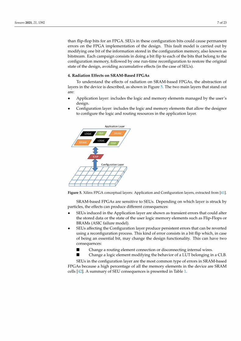
4. Radiation Effects on SRAM-Based FPGAs
To understand the effects of radiation on SRAM-based FPGAs, the abstraction oflayers in the device is described, as shown in Figure 5. The two main layers that stand outare:
• Application layer: includes the logic and memory elements managed by the user’sdesign.
• Configuration layer: includes the logic and memory elements that allow the designerto configure the logic and routing resources in the application layer.
Sensors 2021, 21, x FOR PEER REVIEW 7 of 24
For some of the above solutions, the ASIC failure model (errors into the user memory elements like sequential logic of the target circuits) is not always supported. This is be-cause the vulnerability of SRAM-based FPGAs designs to soft errors is higher than ASIC implementations because of the resources dedicated to memory for programming the board, not for the circuit (device configuration memory). As a rough comparison, the number of the user memory bits can be 10 times higher than RAM bits and 300 times higher than flip-flop bits for an FPGA. SEUs in these configuration bits could cause per-manent errors on the FPGA implementation of the design. This fault model is carried out by modifying one bit of the information stored in the configuration memory, also known as bitstream. Each campaign consists in doing a bit flip to each of the bits that belong to the configuration memory, followed by one run-time reconfiguration to restore the origi-nal state of the design, avoiding accumulative effects (in the case of SEUs).
4. Radiation Effects on SRAM-Based FPGAs To understand the effects of radiation on SRAM-based FPGAs, the abstraction of lay-
ers in the device is described, as shown in Figure 5. The two main layers that stand out are: • Application layer: includes the logic and memory elements managed by the user’s
design. • Configuration layer: includes the logic and memory elements that allow the designer
to configure the logic and routing resources in the application layer.
Figure 5. Xilinx FPGA conceptual layers: Application and Configuration layers, extracted from [41].
SRAM-based FPGAs are sensitive to SEUs. Depending on which layer is struck by particles, the effects can produce different consequences: • SEUs induced in the Application layer are shown as transient errors that could alter
the stored data or the state of the user logic memory elements such as Flip-Flops or BRAMs (ASIC failure model).
• SEUs affecting the Configuration layer produce persistent errors that can be reverted using a reconfiguration process. This kind of error consists in a bit flip which, in case of being an essential bit, may change the design functionality. This can have two con-sequences:
Change a routing element connection or disconnecting internal wires. Change a logic element modifying the behavior of a LUT belonging in a CLB.
SEUs in the configuration layer are the most common type of errors in SRAM-based FPGAs because a high percentage of all the memory elements in the device are SRAM cells [42]. A summary of SEU consequences is presented in Table 1.
Figure 5. Xilinx FPGA conceptual layers: Application and Configuration layers, extracted from [41].
SRAM-based FPGAs are sensitive to SEUs. Depending on which layer is struck byparticles, the effects can produce different consequences:
• SEUs induced in the Application layer are shown as transient errors that could alterthe stored data or the state of the user logic memory elements such as Flip-Flops orBRAMs (ASIC failure model).
• SEUs affecting the Configuration layer produce persistent errors that can be revertedusing a reconfiguration process. This kind of error consists in a bit flip which, in caseof being an essential bit, may change the design functionality. This can have twoconsequences:
� Change a routing element connection or disconnecting internal wires.� Change a logic element modifying the behavior of a LUT belonging in a CLB.
SEUs in the configuration layer are the most common type of errors in SRAM-basedFPGAs because a high percentage of all the memory elements in the device are SRAMcells [42]. A summary of SEU consequences is presented in Table 1.

Sensors 2021, 21, 1392 8 of 23
Table 1. Consequences in SRAM-based FPGAs [42].
Layer Element SEU Consequence
ConfigurationLayer
Routing
Muxes Wrong input selection, open net,wrongly driven or left open
PIP Wrong connection odisconnection between nets
Buffers Output net wrongly driven orleft open
Logic
LUT Wrong function inputs andoutputs
Control bits Wrong function inputs andoutputs
Tie Offs Wrong function initialization
Application layerRAM Blocks Wrong application data
CLB Flip-flops Wrong application data or state
5. Fault-Tolerant Techniques for FPGAs Based on Reconfiguration
This section is focused on SEUs affecting the configuration layer, as they are morelikely to occur. To overcome their effects, some techniques that exploit the particularreconfigurable capabilities of the FPGAs to detect and correct persistent errors in theconfiguration memory are detailed next:
• Scrubbing is a technique used to correct and prevent errors in the information stored inmemory. In FPGAs, scrubbing can be used to mitigate both persistent errors in SRAMcells (i.e., the configuration memory) and transient errors in user-memory elementssuch as BRAMs. To perform configuration memory scrubbing, the configurationmemory data must be read sequentially from the start to the end and compared to theoriginal configuration bitstream or an error check code such as a cyclic redundancycheck (CRC) [43].
• Dynamic partial reconfiguration allows run-time reconfiguration without applicationlayer interruption. This technique cannot detect errors by itself, so it must be combinedwith other error detection techniques such as those based on redundancy. Thesecorrection techniques take advantage of the subdivision of the configuration memoryinto frames, which contain information related to the configuration of specific parts ofthe design.
All the features presented in the previous sections are useful to understand the prin-ciples that drive an FPGA reliability analysis and the related fault injection tools forFPGA designers.
6. An Emulation Framework for Fault Injection
At this point, a step by step tutorial that describes the fault injection tool based onemulation is presented. The setup is based on Xilinx technology. The main modules thatmake up the system are the following:
• The LogiCORE IP Soft Error Mitigation (SEM) Controller version 4.1 [44].• A Nexys 4 DDR board based on the latest Artix-7™ FPGA from Xilinx [45].• A design under test (DUT) implemented for FPGA, in order to measure its depend-
ability in case of soft errors.• A universal asynchronous receiver transmitter (UART) module to implement commu-
nication between both FPGA and host.
An overview of the whole system is explained next.

Sensors 2021, 21, 1392 9 of 23
6.1. Soft Error Mitigation (SEM) IP Controller
SEM IP core is the fault injection engine for the emulation process. This IP core,supported by Xilinx, is a solution to detect and correct soft errors in the ConfigurationMemory of Xilinx FPGAs.
This module can read the configuration memory to look for errors. In case of discover-ing any altered bit, it is flipped by the SEM IP to correct it. This ability to read and write intothe configuration memory is used to manage the fault injection in a non-invasive way. Themanager based on SEM IP could inject bit flips into the configuration memory, testing thereliability of the solution implemented for an FPGA after the injection. SEM IP controller isemployed because it is the only tool in Xilinx FPGAs that allows checking the status of theConfiguration Memory of the devices to look for faults. Customized controllers were notconsidered as SEM IP was already designed, validated and tested by the manufacturer ofthe boards.
In order to add the SEM IP core to a Vivado project, as it can be seen in Figure 6, itrequires to be instantiated from the IP catalog.
Sensors 2021, 21, x FOR PEER REVIEW 9 of 24
into the configuration memory is used to manage the fault injection in a non-invasive way. The manager based on SEM IP could inject bit flips into the configuration memory, testing the reliability of the solution implemented for an FPGA after the injection. SEM IP con-troller is employed because it is the only tool in Xilinx FPGAs that allows checking the status of the Configuration Memory of the devices to look for faults. Customized control-lers were not considered as SEM IP was already designed, validated and tested by the manufacturer of the boards.
In order to add the SEM IP core to a Vivado project, as it can be seen in Figure 6, it requires to be instantiated from the IP catalog.
Figure 6. SEM IP entity.
To do so: • The clock input signal (clk) should be mapped to the global clock of the design. • The Monitor Interface is an UART that serializes status information generated by the
SEM IP controller for serial transmission between the host computer and the FPGA over the TX/RX lines: Monitor RX signal receives as inputs the commands that SEM IP core interprets
in order to perform functions like, for example, injections. Monitor TX signal reports from the SEM IP core, the new states achieved among
these: idle, initialization, observation, injection, correction, fatal error and classi-fication.
Other signals will be described in later sections. Finally, it is important to remark that the FPGA families supported by the SEM IP core are the Zynq-7000 all Programmable SoC and the 7 Series.
6.2. Nexys 4 DDR Based on Artix-7 FPGA Among all the compatible FPGAs, the supported device chosen for this tutorial has
been the Nexys 4 DDR based on an Artix-7 (15,850 logic slices, consisting of four 6-input LUTs and 8 flip-flops).
For the implementation of the fault injection platform based on the SEM IP core pre-sented in this tutorial, the next resources are used to automatize the injection functionality and its monitoring services: • Peripheral module (Pmod) ports, for the serial communication tasks between the
FPGA and the computer, supporting monitoring functions like send and receive data. The Pmod is an input/output interface board, developed by Digilent, that enables a simple connection between the FPGA and other standardized sockets from other ex-ternal devices or even computers. Pmod ports avoid welding wires to the FPGA as they are convenient and easy to plug modules.
Figure 6. SEM IP entity.
To do so:
• The clock input signal (clk) should be mapped to the global clock of the design.• The Monitor Interface is an UART that serializes status information generated by the
SEM IP controller for serial transmission between the host computer and the FPGAover the TX/RX lines:
� Monitor RX signal receives as inputs the commands that SEM IP core interpretsin order to perform functions like, for example, injections.
� Monitor TX signal reports from the SEM IP core, the new states achievedamong these: idle, initialization, observation, injection, correction, fatal errorand classification.
Other signals will be described in later sections. Finally, it is important to remark thatthe FPGA families supported by the SEM IP core are the Zynq-7000 all Programmable SoCand the 7 Series.
6.2. Nexys 4 DDR Based on Artix-7 FPGA
Among all the compatible FPGAs, the supported device chosen for this tutorial hasbeen the Nexys 4 DDR based on an Artix-7 (15,850 logic slices, consisting of four 6-inputLUTs and 8 flip-flops).
For the implementation of the fault injection platform based on the SEM IP core pre-sented in this tutorial, the next resources are used to automatize the injection functionalityand its monitoring services:
• Peripheral module (Pmod) ports, for the serial communication tasks between theFPGA and the computer, supporting monitoring functions like send and receive data.

Sensors 2021, 21, 1392 10 of 23
The Pmod is an input/output interface board, developed by Digilent, that enablesa simple connection between the FPGA and other standardized sockets from otherexternal devices or even computers. Pmod ports avoid welding wires to the FPGA asthey are convenient and easy to plug modules.
• FPGA configuration reset button, allows to reset the FPGA after each fault injection.Note that because of an emulated SEU which permanently alters the configurationlayer, the FPGA requires to be reset. After these reset conditions, the FPGA must beconfigured again loading the original bitstream. For this purpose, a flash memoryincluded in the board contains a copy of the stored design, in order to automatizethe configuration after each fault is injected, avoiding a manually load through theVivado tool.
6.3. Design for the Experimental Set-Up
The proposed structure for the experimental set-up in this tutorial is shown in Figure 7.It consists of: a ROM, where the input stimuli are contained; a twin circuit CIRCUIT 1and CIRCUIT 2 with the original behavior, and a checker module (CHCK) that performsa comparison between the two copies in order to detect if any error happened. OnlyCIRCUIT 1 is considered as the DUT where errors will be injected by the SEM IP controller,and CIRCUIT 2 keeps the original behavior and acts as a golden copy that, by means ofa comparator (CHCK), validates if the outputs from CIRCUIT 1 after injection match theexpected values.
Sensors 2021, 21, x FOR PEER REVIEW 10 of 24
• FPGA configuration reset button, allows to reset the FPGA after each fault injection. Note that because of an emulated SEU which permanently alters the configuration layer, the FPGA requires to be reset. After these reset conditions, the FPGA must be configured again loading the original bitstream. For this purpose, a flash memory included in the board contains a copy of the stored design, in order to automatize the configuration after each fault is injected, avoiding a manually load through the Vi-vado tool.
6.3. Design for the Experimental Set-Up The proposed structure for the experimental set-up in this tutorial is shown in Figure
7. It consists of: a ROM, where the input stimuli are contained; a twin circuit CIRCUIT 1 and CIRCUIT 2 with the original behavior, and a checker module (CHCK) that performs a comparison between the two copies in order to detect if any error happened. Only CIR-CUIT 1 is considered as the DUT where errors will be injected by the SEM IP controller, and CIRCUIT 2 keeps the original behavior and acts as a golden copy that, by means of a comparator (CHCK), validates if the outputs from CIRCUIT 1 after injection match the expected values.
The same validation could also be done by producing a pre-processed output file free of errors (with the expected outputs). The output of the DUT would then be compared to the output file for the same circuit in presence of SEUs. After that, a data post-processing in the host PC calculates the number of errors detected.
Figure 7. Design for the experimental setup.
In http://www.nebrija.es/aries/acme.htm an online copy of a real project based on an FIR filter structure can be found with a brief document that includes all the process, step by step. This example can be used as a case study to make a full demo of the fault injection process.
6.4. Universal Asynchronous Receiver-Transmitter The UART module is included as another part of the design to manage serial com-
munications between the host computer and the FPGA over the serial_out line as is shown in Figure 8.
Figure 7. Design for the experimental setup.
The same validation could also be done by producing a pre-processed output file freeof errors (with the expected outputs). The output of the DUT would then be compared tothe output file for the same circuit in presence of SEUs. After that, a data post-processingin the host PC calculates the number of errors detected.
In http://www.nebrija.es/aries/acme.htm an online copy of a real project based onan FIR filter structure can be found with a brief document that includes all the process,step by step. This example can be used as a case study to make a full demo of the faultinjection process.
6.4. Universal Asynchronous Receiver-Transmitter
The UART module is included as another part of the design to manage serial commu-nications between the host computer and the FPGA over the serial_out line as is shownin Figure 8.

Sensors 2021, 21, 1392 11 of 23Sensors 2021, 21, x FOR PEER REVIEW 11 of 24
Figure 8. UART model.
This UART allows a monitor process similar to the one supported by the SEM IP controller, but in this case, it is used to send to the host computer if there was an error in the output of the system after each injected SEU. In order to connect this UART model to the host computer, another USB to UART converter such as a Pmod USBUART has been used, and the mapping must be included in the constraint file again. As a summary (Fig-ure 9), the design implemented in the Nexys 4 DDR board is composed of: • DUT composed of ROM, CIRCUIT 1, CIRCUIT 2 and the CHCK. • UART for communication of the errors. • SEM IP core included in Vivado.
Figure 8. UART model.
This UART allows a monitor process similar to the one supported by the SEM IPcontroller, but in this case, it is used to send to the host computer if there was an error in theoutput of the system after each injected SEU. In order to connect this UART model to thehost computer, another USB to UART converter such as a Pmod USBUART has been used,and the mapping must be included in the constraint file again. As a summary (Figure 9),the design implemented in the Nexys 4 DDR board is composed of:
• DUT composed of ROM, CIRCUIT 1, CIRCUIT 2 and the CHCK.• UART for communication of the errors.• SEM IP core included in Vivado.Sensors 2021, 21, x FOR PEER REVIEW 12 of 24
Figure 9. Source files overview.
7. Emulation Workflow Step by Step Next, the different steps required to implement fault injection emulation based on
the architecture defined in the previous section will be described. In this section it will be shown that two projects will be necessary. The first one is the main workspace, where the design for the experimental set-up, the UART and the SEM IP controller will be integrated for the target reliability tests. The second one is only necessary to extract and reutilize the SEM IP core files into the first one and it will be removed after this task is completed.
Now, a step by step description of the emulation is detailed. First, a new RTL project for Vivado (the first one), is created including the HDL (Table 2) files that refer to both the design for the experimental set-up and UART modules. The inclusion of the SEM IP con-troller will be shown in detail later.
Table 2. Projects files before SEM IP core.
Modules Files
Design for the experimental set-up
rom.vhd circuit1.vhd circuit 2.vhd checker.vhd
UART uart.vhd
Figure 9. Source files overview.

Sensors 2021, 21, 1392 12 of 23
7. Emulation Workflow Step by Step
Next, the different steps required to implement fault injection emulation based onthe architecture defined in the previous section will be described. In this section it will beshown that two projects will be necessary. The first one is the main workspace, where thedesign for the experimental set-up, the UART and the SEM IP controller will be integratedfor the target reliability tests. The second one is only necessary to extract and reutilize theSEM IP core files into the first one and it will be removed after this task is completed.
Now, a step by step description of the emulation is detailed. First, a new RTL projectfor Vivado (the first one), is created including the HDL (Table 2) files that refer to boththe design for the experimental set-up and UART modules. The inclusion of the SEM IPcontroller will be shown in detail later.
Table 2. Projects files before SEM IP core.
Modules Files
Design for the experimental set-up
rom.vhdcircuit1.vhdcircuit 2.vhdchecker.vhd
UART uart.vhd
Also, at this point the board model has to be selected. For this tutorial, the board isa Nexys 4 DDR with Artix-7 FPGA. Once the DUT, the golden copy and the checker areimplemented, and before continuing with the process, a good practice would be to simulateand check the design for the experimental set-up. For instance, Figure 10a, the CHCKoutput is included for a sample circuit with no injected errors. In this trivial example bothoutputs defined as Y0 (CIRCUIT 1) and Y1 (CIRCUIT 2) are equal in the whole simulation,and the checker output (ERR) takes a value of 0, which indicates that no errors occur.
Sensors 2021, 21, x FOR PEER REVIEW 13 of 24
Also, at this point the board model has to be selected. For this tutorial, the board is a Nexys 4 DDR with Artix-7 FPGA. Once the DUT, the golden copy and the checker are implemented, and before continuing with the process, a good practice would be to simu-late and check the design for the experimental set-up. For instance, Figure
(a)
(b)
Figure 10. (a) Simulation without an SEU. (b) Simulation with an SEU.
On the contrary, the next simulation (Figure 10b) shows an error detected by the checker due to an SEU inserted via force command in the DUT. It can be observed that both outputs are different (Y0 has a value of ffff and Y1 has the correct value of 03ba) and the checker detects the error changing its output, ERR (at 168 ns), with a code different from the right one.
After the verification of the experimental environment, the SEM IP controller is re-quired to be instantiated in order to enable and control the fault injection process. This core can be found in the Vivado IP Catalog, and its maximum clock frequency meets the frequency of the board (for Nexys 4 the threshold is 100 MHz). Below this frequency the SEM IP controller works properly. Also, the controller options must be enabled.
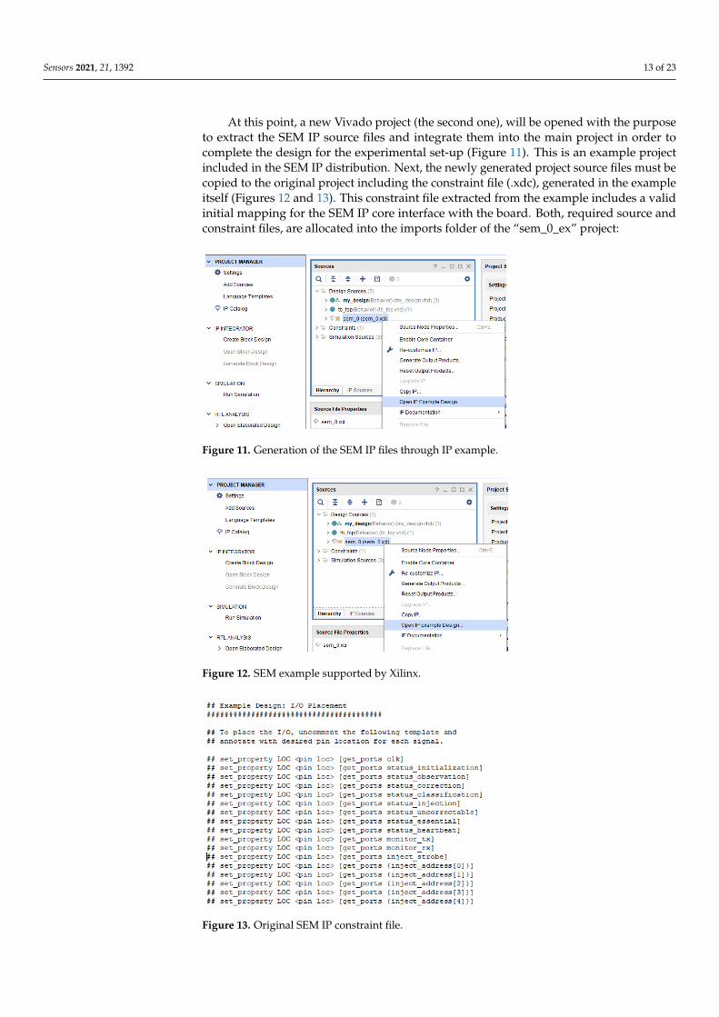
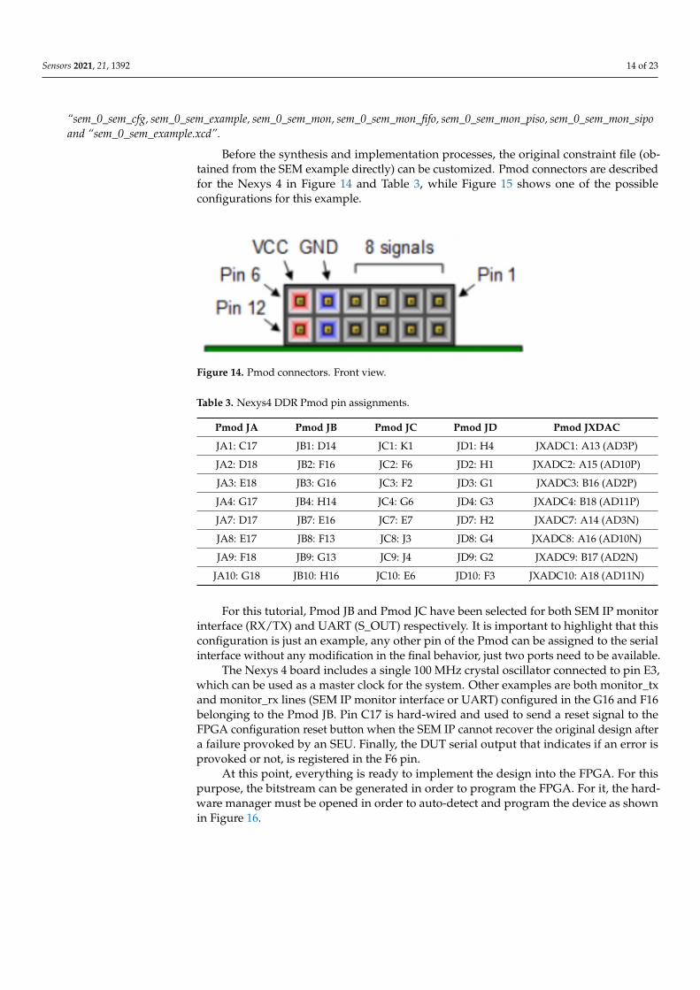
At this point, a new Vivado project (the second one), will be opened with the purpose to extract the SEM IP source files and integrate them into the main project in order to complete the design for the experimental set-up (Figure 11). This is an example project included in the SEM IP distribution. Next, the newly generated project source files must be copied to the original project including the constraint file (.xdc), generated in the ex-ample itself (Figures 12 and 13). This constraint file extracted from the example includes a valid initial mapping for the SEM IP core interface with the board. Both, required source and constraint files, are allocated into the imports folder of the “sem_0_ex” project:
“sem_0_sem_cfg, sem_0_sem_example, sem_0_sem_mon, sem_0_sem_mon_fifo, sem_0_sem_mon_piso, sem_0_sem_mon_sipo and “sem_0_sem_example.xcd”.
Figure 10. (a) Simulation without an SEU. (b) Simulation with an SEU.
On the contrary, the next simulation (Figure 10b) shows an error detected by thechecker due to an SEU inserted via force command in the DUT. It can be observed thatboth outputs are different (Y0 has a value of ffff and Y1 has the correct value of 03ba) andthe checker detects the error changing its output, ERR (at 168 ns), with a code differentfrom the right one.
After the verification of the experimental environment, the SEM IP controller isrequired to be instantiated in order to enable and control the fault injection process. Thiscore can be found in the Vivado IP Catalog, and its maximum clock frequency meets thefrequency of the board (for Nexys 4 the threshold is 100 MHz). Below this frequency theSEM IP controller works properly. Also, the controller options must be enabled.
Sensors 2021, 21, 1392 13 of 23
At this point, a new Vivado project (the second one), will be opened with the purposeto extract the SEM IP source files and integrate them into the main project in order tocomplete the design for the experimental set-up (Figure 11). This is an example projectincluded in the SEM IP distribution. Next, the newly generated project source files must becopied to the original project including the constraint file (.xdc), generated in the exampleitself (Figures 12 and 13). This constraint file extracted from the example includes a validinitial mapping for the SEM IP core interface with the board. Both, required source andconstraint files, are allocated into the imports folder of the “sem_0_ex” project:
Sensors 2021, 21, x FOR PEER REVIEW 14 of 24
Figure 11. Generation of the SEM IP files through IP example.
Figure 12. SEM example supported by Xilinx.
Figure 13. Original SEM IP constraint file.
Before the synthesis and implementation processes, the original constraint file (ob-tained from the SEM example directly) can be customized. Pmod connectors are described for the Nexys 4 in Figure 14 and Table 3, while Figure 15 shows one of the possible con-figurations for this example.
Figure 11. Generation of the SEM IP files through IP example.
Sensors 2021, 21, x FOR PEER REVIEW 14 of 24
Figure 11. Generation of the SEM IP files through IP example.
Figure 12. SEM example supported by Xilinx.
Figure 13. Original SEM IP constraint file.
Before the synthesis and implementation processes, the original constraint file (ob-tained from the SEM example directly) can be customized. Pmod connectors are described for the Nexys 4 in Figure 14 and Table 3, while Figure 15 shows one of the possible con-figurations for this example.
Figure 12. SEM example supported by Xilinx.
Sensors 2021, 21, x FOR PEER REVIEW 14 of 24
Figure 11. Generation of the SEM IP files through IP example.
Figure 12. SEM example supported by Xilinx.
Figure 13. Original SEM IP constraint file.
Before the synthesis and implementation processes, the original constraint file (ob-tained from the SEM example directly) can be customized. Pmod connectors are described for the Nexys 4 in Figure 14 and Table 3, while Figure 15 shows one of the possible con-figurations for this example.
Figure 13. Original SEM IP constraint file.
Sensors 2021, 21, 1392 14 of 23
“sem_0_sem_cfg, sem_0_sem_example, sem_0_sem_mon, sem_0_sem_mon_fifo, sem_0_sem_mon_piso, sem_0_sem_mon_sipoand “sem_0_sem_example.xcd”.
Before the synthesis and implementation processes, the original constraint file (ob-tained from the SEM example directly) can be customized. Pmod connectors are describedfor the Nexys 4 in Figure 14 and Table 3, while Figure 15 shows one of the possibleconfigurations for this example.
Sensors 2021, 21, x FOR PEER REVIEW 15 of 24
Figure 14. Pmod connectors. Front view.
Table 3. Nexys4 DDR Pmod pin assignments.
Pmod JA Pmod JB Pmod JC Pmod JD Pmod JXDAC JA1: C17 JB1: D14 JC1: K1 JD1: H4 JXADC1: A13 (AD3P) JA2: D18 JB2: F16 JC2: F6 JD2: H1 JXADC2: A15 (AD10P) JA3: E18 JB3: G16 JC3: F2 JD3: G1 JXADC3: B16 (AD2P) JA4: G17 JB4: H14 JC4: G6 JD4: G3 JXADC4: B18 (AD11P) JA7: D17 JB7: E16 JC7: E7 JD7: H2 JXADC7: A14 (AD3N) JA8: E17 JB8: F13 JC8: J3 JD8: G4 JXADC8: A16 (AD10N) JA9: F18 JB9: G13 JC9: J4 JD9: G2 JXADC9: B17 (AD2N)
JA10: G18 JB10: H16 JC10: E6 JD10: F3 JXADC10: A18 (AD11N)
Figure 15. Constraint file example.
For this tutorial, Pmod JB and Pmod JC have been selected for both SEM IP monitor interface (RX/TX) and UART (S_OUT) respectively. It is important to highlight that this configuration is just an example, any other pin of the Pmod can be assigned to the serial interface without any modification in the final behavior, just two ports need to be availa-ble.
Figure 14. Pmod connectors. Front view.
Table 3. Nexys4 DDR Pmod pin assignments.
Pmod JA Pmod JB Pmod JC Pmod JD Pmod JXDAC
JA1: C17 JB1: D14 JC1: K1 JD1: H4 JXADC1: A13 (AD3P)
JA2: D18 JB2: F16 JC2: F6 JD2: H1 JXADC2: A15 (AD10P)
JA3: E18 JB3: G16 JC3: F2 JD3: G1 JXADC3: B16 (AD2P)
JA4: G17 JB4: H14 JC4: G6 JD4: G3 JXADC4: B18 (AD11P)
JA7: D17 JB7: E16 JC7: E7 JD7: H2 JXADC7: A14 (AD3N)
JA8: E17 JB8: F13 JC8: J3 JD8: G4 JXADC8: A16 (AD10N)
JA9: F18 JB9: G13 JC9: J4 JD9: G2 JXADC9: B17 (AD2N)
JA10: G18 JB10: H16 JC10: E6 JD10: F3 JXADC10: A18 (AD11N)
For this tutorial, Pmod JB and Pmod JC have been selected for both SEM IP monitorinterface (RX/TX) and UART (S_OUT) respectively. It is important to highlight that thisconfiguration is just an example, any other pin of the Pmod can be assigned to the serialinterface without any modification in the final behavior, just two ports need to be available.
The Nexys 4 board includes a single 100 MHz crystal oscillator connected to pin E3,which can be used as a master clock for the system. Other examples are both monitor_txand monitor_rx lines (SEM IP monitor interface or UART) configured in the G16 and F16belonging to the Pmod JB. Pin C17 is hard-wired and used to send a reset signal to theFPGA configuration reset button when the SEM IP cannot recover the original design aftera failure provoked by an SEU. Finally, the DUT serial output that indicates if an error isprovoked or not, is registered in the F6 pin.
At this point, everything is ready to implement the design into the FPGA. For thispurpose, the bitstream can be generated in order to program the FPGA. For it, the hard-ware manager must be opened in order to auto-detect and program the device as shownin Figure 16.

Sensors 2021, 21, 1392 15 of 23
Sensors 2021, 21, x FOR PEER REVIEW 15 of 24
Figure 14. Pmod connectors. Front view.
Table 3. Nexys4 DDR Pmod pin assignments.
Pmod JA Pmod JB Pmod JC Pmod JD Pmod JXDAC JA1: C17 JB1: D14 JC1: K1 JD1: H4 JXADC1: A13 (AD3P) JA2: D18 JB2: F16 JC2: F6 JD2: H1 JXADC2: A15 (AD10P) JA3: E18 JB3: G16 JC3: F2 JD3: G1 JXADC3: B16 (AD2P) JA4: G17 JB4: H14 JC4: G6 JD4: G3 JXADC4: B18 (AD11P) JA7: D17 JB7: E16 JC7: E7 JD7: H2 JXADC7: A14 (AD3N) JA8: E17 JB8: F13 JC8: J3 JD8: G4 JXADC8: A16 (AD10N) JA9: F18 JB9: G13 JC9: J4 JD9: G2 JXADC9: B17 (AD2N)
JA10: G18 JB10: H16 JC10: E6 JD10: F3 JXADC10: A18 (AD11N)
Figure 15. Constraint file example.
For this tutorial, Pmod JB and Pmod JC have been selected for both SEM IP monitor interface (RX/TX) and UART (S_OUT) respectively. It is important to highlight that this configuration is just an example, any other pin of the Pmod can be assigned to the serial interface without any modification in the final behavior, just two ports need to be availa-ble.
Figure 15. Constraint file example.
Sensors 2021, 21, x FOR PEER REVIEW 16 of 24
The Nexys 4 board includes a single 100 MHz crystal oscillator connected to pin E3, which can be used as a master clock for the system. Other examples are both monitor_tx and monitor_rx lines (SEM IP monitor interface or UART) configured in the G16 and F16 belonging to the Pmod JB. Pin C17 is hard-wired and used to send a reset signal to the FPGA configuration reset button when the SEM IP cannot recover the original design after a failure provoked by an SEU. Finally, the DUT serial output that indicates if an error is provoked or not, is registered in the F6 pin.
At this point, everything is ready to implement the design into the FPGA. For this purpose, the bitstream can be generated in order to program the FPGA. For it, the hard-ware manager must be opened in order to auto-detect and program the device as shown in Figure 16.
Figure 16. Program SRAM configuration memory.
Once the device has been loaded with the resultant bitstream, the appearance of the board is the one included in Figure 17. As it can be noticed, both green LEDs are lit. The first one is the “FPGA programming done” LED and the second is defined in the con-straint file as an SEM IP signal denoting that the module is in observation mode. There-fore, it indicates that the SEM IP is ready to operate.
Figure 17. Device programmed with SEM IP observation mode (H17 led).
Another SEM IP output mapped through the constraint file is the status uncorrecta-ble in the pin C17. A bridge between this pin and the FPGA configuration reset button is
Done led
Observation
l d
Figure 16. Program SRAM configuration memory.
Once the device has been loaded with the resultant bitstream, the appearance of theboard is the one included in Figure 17. As it can be noticed, both green LEDs are lit. Thefirst one is the “FPGA programming done” LED and the second is defined in the constraintfile as an SEM IP signal denoting that the module is in observation mode. Therefore, itindicates that the SEM IP is ready to operate.

Sensors 2021, 21, 1392 16 of 23
Sensors 2021, 21, x FOR PEER REVIEW 16 of 24
The Nexys 4 board includes a single 100 MHz crystal oscillator connected to pin E3, which can be used as a master clock for the system. Other examples are both monitor_tx and monitor_rx lines (SEM IP monitor interface or UART) configured in the G16 and F16 belonging to the Pmod JB. Pin C17 is hard-wired and used to send a reset signal to the FPGA configuration reset button when the SEM IP cannot recover the original design after a failure provoked by an SEU. Finally, the DUT serial output that indicates if an error is provoked or not, is registered in the F6 pin.
At this point, everything is ready to implement the design into the FPGA. For this purpose, the bitstream can be generated in order to program the FPGA. For it, the hard-ware manager must be opened in order to auto-detect and program the device as shown in Figure 16.
Figure 16. Program SRAM configuration memory.
Once the device has been loaded with the resultant bitstream, the appearance of the board is the one included in Figure 17. As it can be noticed, both green LEDs are lit. The first one is the “FPGA programming done” LED and the second is defined in the con-straint file as an SEM IP signal denoting that the module is in observation mode. There-fore, it indicates that the SEM IP is ready to operate.
Figure 17. Device programmed with SEM IP observation mode (H17 led).
Another SEM IP output mapped through the constraint file is the status uncorrecta-ble in the pin C17. A bridge between this pin and the FPGA configuration reset button is
Done led
Observation
l d
Figure 17. Device programmed with SEM IP observation mode (H17 led).
Another SEM IP output mapped through the constraint file is the status uncorrectablein the pin C17. A bridge between this pin and the FPGA configuration reset button is done,for auto-reconfiguration purposes. This reset works with negative logic, so it requires to beinverted in the original sem_0_sem_example file:
status_uncorrectable ≤ not (status_uncorrectable_internal);Another important point is that, since the Artix 7 FPGA is based on SRAM volatile
memory, it relies on the integrated Quad-SPI flash memory to store the configurationbetween power cycles. When this flash device has been programmed, it can automaticallyreconfigure the FPGA at a subsequent power-on or reset event as determined by themode JP1 jumper setting (Figure 18). Regardless of which board is going to be used, it isrecommended to include a flash memory because of the constant need for reconfiguration,in order to automatize the process.
Sensors 2021, 21, x FOR PEER REVIEW 17 of 24
done, for auto-reconfiguration purposes. This reset works with negative logic, so it re-quires to be inverted in the original sem_0_sem_example file:
status_uncorrectable ≤ not (status_uncorrectable_internal);
Another important point is that, since the Artix 7 FPGA is based on SRAM volatile memory, it relies on the integrated Quad-SPI flash memory to store the configuration be-tween power cycles. When this flash device has been programmed, it can automatically reconfigure the FPGA at a subsequent power-on or reset event as determined by the mode JP1 jumper setting (Figure 18). Regardless of which board is going to be used, it is recom-mended to include a flash memory because of the constant need for reconfiguration, in order to automatize the process.
Figure 18. Jumper for SPI Quad mode Flash programming mode.
As can be noticed in Figure 19, in order to use it, this memory has to be added through the Vivado hardware manager and it allows the FPGA configuration memory to be auto-reprogrammed from the Quad-SPI Flash (Spansion part number S25FL128S) previously configured with the original design.
Figure 19. Flash memory device for Nexys 4 DDR.
This original design needs to be saved in a.bin file as shown in both Figures 20 and 21.
Figure 20. File generation for flash memory (.bin).
Figure 18. Jumper for SPI Quad mode Flash programming mode.
As can be noticed in Figure 19, in order to use it, this memory has to be added throughthe Vivado hardware manager and it allows the FPGA configuration memory to be auto-reprogrammed from the Quad-SPI Flash (Spansion part number S25FL128S) previouslyconfigured with the original design.
Sensors 2021, 21, x FOR PEER REVIEW 17 of 24
done, for auto-reconfiguration purposes. This reset works with negative logic, so it re-quires to be inverted in the original sem_0_sem_example file:
status_uncorrectable ≤ not (status_uncorrectable_internal);
Another important point is that, since the Artix 7 FPGA is based on SRAM volatile memory, it relies on the integrated Quad-SPI flash memory to store the configuration be-tween power cycles. When this flash device has been programmed, it can automatically reconfigure the FPGA at a subsequent power-on or reset event as determined by the mode JP1 jumper setting (Figure 18). Regardless of which board is going to be used, it is recom-mended to include a flash memory because of the constant need for reconfiguration, in order to automatize the process.
Figure 18. Jumper for SPI Quad mode Flash programming mode.
As can be noticed in Figure 19, in order to use it, this memory has to be added through the Vivado hardware manager and it allows the FPGA configuration memory to be auto-reprogrammed from the Quad-SPI Flash (Spansion part number S25FL128S) previously configured with the original design.
Figure 19. Flash memory device for Nexys 4 DDR.
This original design needs to be saved in a.bin file as shown in both Figures 20 and 21.
Figure 20. File generation for flash memory (.bin).
Figure 19. Flash memory device for Nexys 4 DDR.
This original design needs to be saved in a.bin file as shown in both Figures 20 and 21.

Sensors 2021, 21, 1392 17 of 23
Sensors 2021, 21, x FOR PEER REVIEW 17 of 24
done, for auto-reconfiguration purposes. This reset works with negative logic, so it re-quires to be inverted in the original sem_0_sem_example file:
status_uncorrectable ≤ not (status_uncorrectable_internal);
Another important point is that, since the Artix 7 FPGA is based on SRAM volatile memory, it relies on the integrated Quad-SPI flash memory to store the configuration be-tween power cycles. When this flash device has been programmed, it can automatically reconfigure the FPGA at a subsequent power-on or reset event as determined by the mode JP1 jumper setting (Figure 18). Regardless of which board is going to be used, it is recom-mended to include a flash memory because of the constant need for reconfiguration, in order to automatize the process.
Figure 18. Jumper for SPI Quad mode Flash programming mode.
As can be noticed in Figure 19, in order to use it, this memory has to be added through the Vivado hardware manager and it allows the FPGA configuration memory to be auto-reprogrammed from the Quad-SPI Flash (Spansion part number S25FL128S) previously configured with the original design.
Figure 19. Flash memory device for Nexys 4 DDR.
This original design needs to be saved in a.bin file as shown in both Figures 20 and 21.
Figure 20. File generation for flash memory (.bin).
Figure 20. File generation for flash memory (.bin).Sensors 2021, 21, x FOR PEER REVIEW 18 of 24
Figure 21. Flash memory load.
It should be mentioned that the next couple of lines must be included in the constraint file to enable the possibility to load the original bitstream from the flash memory:
set_property BITSTREAM.CONFIG.SPI_BUSWIDTH 4 [current_design] set_property CONFIG_MODE SPIx4 [current_design]
Once the manager has been configured and before proceeding with the interactive process, let us describe the different states that can be adopted by the SEM IP. • Initialization (01): Once the configuration has been completed, the FPGA sends the
global set/reset signal and the SEM IP controller starts. If the initialization process has been completed in the correct way, the controller moves to the observation state showing in the monitor the next (Figure 22):
Figure 22. SEM IP Controller initialized. Ready to receive commands for the injection process.
• Observation (02): When the controller is in the observation state, status_observation variable is set, and the SEM IP controller watches the FPGA configuration looking for errors. In case of an error, the controller transits to the correction state to recover the original configuration automatically. If no error exists, when the SEM IP control-ler receives a command, it is executed. Both “enter idle” (moves to idle state) and “status report” commands are supported in the current state.
• Correction (04): When the controller is in the correction state, status_correction varia-ble is set. If the SEM IP is setup for correction to repair or correction by enhanced repair, it tries to correct the error through algorithmic methods. If the error can be corrected, the SEM IP instance uses the partial reconfiguration feature in order to modify the affected frame with the good information and resets the status_uncorrect-able variable. In case that the error cannot be corrected, the controller sets the sta-tus_uncorrectable variable. When this situation occurs, the FPGA must be reconfig-ured. Once correction is completed, the controller moves back to observation state.
Figure 21. Flash memory load.
It should be mentioned that the next couple of lines must be included in the constraintfile to enable the possibility to load the original bitstream from the flash memory:
set_property BITSTREAM.CONFIG.SPI_BUSWIDTH 4 [current_design]set_property CONFIG_MODE SPIx4 [current_design]Once the manager has been configured and before proceeding with the interactive
process, let us describe the different states that can be adopted by the SEM IP.
• Initialization (01): Once the configuration has been completed, the FPGA sends theglobal set/reset signal and the SEM IP controller starts. If the initialization processhas been completed in the correct way, the controller moves to the observation stateshowing in the monitor the next (Figure 22):
Sensors 2021, 21, x FOR PEER REVIEW 18 of 24
Figure 21. Flash memory load.
It should be mentioned that the next couple of lines must be included in the constraint file to enable the possibility to load the original bitstream from the flash memory:
set_property BITSTREAM.CONFIG.SPI_BUSWIDTH 4 [current_design] set_property CONFIG_MODE SPIx4 [current_design]
Once the manager has been configured and before proceeding with the interactive process, let us describe the different states that can be adopted by the SEM IP. • Initialization (01): Once the configuration has been completed, the FPGA sends the
global set/reset signal and the SEM IP controller starts. If the initialization process has been completed in the correct way, the controller moves to the observation state showing in the monitor the next (Figure 22):
Figure 22. SEM IP Controller initialized. Ready to receive commands for the injection process.
• Observation (02): When the controller is in the observation state, status_observation variable is set, and the SEM IP controller watches the FPGA configuration looking for errors. In case of an error, the controller transits to the correction state to recover the original configuration automatically. If no error exists, when the SEM IP control-ler receives a command, it is executed. Both “enter idle” (moves to idle state) and “status report” commands are supported in the current state.
• Correction (04): When the controller is in the correction state, status_correction varia-ble is set. If the SEM IP is setup for correction to repair or correction by enhanced repair, it tries to correct the error through algorithmic methods. If the error can be corrected, the SEM IP instance uses the partial reconfiguration feature in order to modify the affected frame with the good information and resets the status_uncorrect-able variable. In case that the error cannot be corrected, the controller sets the sta-tus_uncorrectable variable. When this situation occurs, the FPGA must be reconfig-ured. Once correction is completed, the controller moves back to observation state.
Figure 22. SEM IP Controller initialized. Ready to receive commands for the injection process.

Sensors 2021, 21, 1392 18 of 23
• Observation (02): When the controller is in the observation state, status_observationvariable is set, and the SEM IP controller watches the FPGA configuration looking forerrors. In case of an error, the controller transits to the correction state to recover theoriginal configuration automatically. If no error exists, when the SEM IP controllerreceives a command, it is executed. Both “enter idle” (moves to idle state) and “statusreport” commands are supported in the current state.
• Correction (04): When the controller is in the correction state, status_correction variableis set. If the SEM IP is setup for correction to repair or correction by enhanced repair,it tries to correct the error through algorithmic methods. If the error can be corrected,the SEM IP instance uses the partial reconfiguration feature in order to modify theaffected frame with the good information and resets the status_uncorrectable variable.In case that the error cannot be corrected, the controller sets the status_uncorrectablevariable. When this situation occurs, the FPGA must be reconfigured. Once correctionis completed, the controller moves back to observation state.
• Idle (00): When the controller reaches this state, it is prepared to execute both errorinjection and software reset commands which are supported in this state.
• Injection (10): When the controller is in this state, the injections action can be performed.It happens when an error injection command is executed from the previous idle state.The emulation of the strike of one SEU into the configuration memory is achievedby flipping the bit which corresponds to the memory address provided in the errorinjection command. After each injection, the controller moves from the injection tothe idle state automatically. At the end of error injection, the controller transits to theobservation state (Figure 23).
Sensors 2021, 21, x FOR PEER REVIEW 19 of 24
• Idle (00): When the controller reaches this state, it is prepared to execute both error injection and software reset commands which are supported in this state.
• Injection (10): When the controller is in this state, the injections action can be per-formed. It happens when an error injection command is executed from the previous idle state. The emulation of the strike of one SEU into the configuration memory is achieved by flipping the bit which corresponds to the memory address provided in the error injection command. After each injection, the controller moves from the in-jection to the idle state automatically. At the end of error injection, the controller transits to the observation state (Figure 23).
Initialization01
Observation02
Idle00
Injection10
I
N
O
Correction04
Automatic
Automatic
Automatic
Figure 23. SEM IP state diagram.
After the SEM IP states have been presented, we are ready to interact with the fault injector manager through the enabled communication ports defined in the constraint file. As it was said in a previous section, connecting a serial peripheral module such as a Pmod USBUART converter to the FPGA port, where both “monitor_tx” (G16) and “monitor_rx” (F16) signals has been mapped from the constraints file (in this case Pmod JA), will allow to send and receive commands from the SEM IP core. In order to undertake this commu-nication, a serial terminal program e.g., “Tera Term” in this tutorial, is used like a monitor interface to register any interaction. As it was mentioned in the SEM IP controller section, the monitor interface (SEM IP UART included) consists, among others, of two signals im-plementing an RS-232 compatible protocol, for a full duplex channel to exchange com-mands and status. The next configuration is used for a Tera Term terminal:
Band: 9600 Settings: 8-N-1 Flow Control: None Terminal Setup: VT100 TX Newline: CR (Terminal transmits CR [0x0D] as end of line) RX Newline: CR+LF (Terminal receives CR [0x0D] as end of line, and expands to CR+LF [0x0D, 0x0A]) Local Echo: NO To configure the communication bit rate, the parameter V_ENABLETIME declared
in the sem_0_sem_mon, which is a MON Shim implementation for communication with external RS232 devices, must be set according the following Equation (1): 𝑉 = 𝑟𝑜𝑢𝑛𝑑 𝑡𝑜 𝑖𝑛𝑡𝑒𝑔𝑒𝑟 𝑖𝑛𝑝𝑢𝑡 𝑐𝑙𝑜𝑐𝑘 𝑓𝑟𝑒𝑐𝑢𝑒𝑛𝑐𝑦16 ∗ 𝑛𝑜𝑚𝑖𝑛𝑎𝑙 𝑏𝑖𝑡𝑟𝑎𝑡𝑒 − 1 (1)
For example, for a baud equal to 9600, the V_ENABLETIME will be 650. If the baud requires to be increase to 230,400, then the V_ENABLETIME will be 26. The command set available from the Error Injection Interface are the following (case sensitive: uppercase): • command sends the controller to the observation state. • I command sends the controller to the idle state. • S command requests a status report.
Figure 23. SEM IP state diagram.
After the SEM IP states have been presented, we are ready to interact with the faultinjector manager through the enabled communication ports defined in the constraintfile. As it was said in a previous section, connecting a serial peripheral module suchas a Pmod USBUART converter to the FPGA port, where both “monitor_tx” (G16) and“monitor_rx” (F16) signals has been mapped from the constraints file (in this case PmodJA), will allow to send and receive commands from the SEM IP core. In order to undertakethis communication, a serial terminal program e.g., “Tera Term” in this tutorial, is usedlike a monitor interface to register any interaction. As it was mentioned in the SEM IPcontroller section, the monitor interface (SEM IP UART included) consists, among others,of two signals implementing an RS-232 compatible protocol, for a full duplex channel toexchange commands and status. The next configuration is used for a Tera Term terminal:
Band: 9600Settings: 8-N-1Flow Control: NoneTerminal Setup: VT100TX Newline: CR (Terminal transmits CR [0x0D] as end of line)RX Newline: CR+LF (Terminal receives CR [0x0D] as end of line, and expands to CR+LF [0x0D,0x0A])

Sensors 2021, 21, 1392 19 of 23
Local Echo: NO
To configure the communication bit rate, the parameter V_ENABLETIME declaredin the sem_0_sem_mon, which is a MON Shim implementation for communication withexternal RS232 devices, must be set according the following Equation (1):
VENABLETIME = round to integer[
input clock f recuency16 ∗ nominal bitrate
]− 1 (1)
For example, for a baud equal to 9600, the V_ENABLETIME will be 650. If the baudrequires to be increase to 230,400, then the V_ENABLETIME will be 26. The command setavailable from the Error Injection Interface are the following (case sensitive: uppercase):
• command sends the controller to the observation state.• I command sends the controller to the idle state.• S command requests a status report.• N command performs an error injection. This command is only supported in the idle
state. The interface is: N {10-digit hex value}• R command performs a software reset. This command is only supported in the idle
state. The interface is: R {2-digit hex value}
All this information is enough to generate the fault injection campaigns for eachconfiguration bit. Obviously, at the same time that commands are sent to the SEM IPcontroller via Pmod1 (JB), the output of the DUT will be received through the Pmod2 (JC)and the number of errors that provoke failures in the output will be counted.
Next section deals with the performance problem for the emulation in SRAM-basedFPGAs. If the campaign is exhaustive around the whole configuration memory, then thetime required to run a fault injection could be excessive.
8. ACME: Speeding Up the Injection Performance
Essential bits defined by Xilinx programs are related to the whole system, including theSEM IP, the ROM, the DUT, the golden copy and the checker (Figure 7). As the objective isto inject in the DUT to validate its fault tolerance against SEUs in the configuration memory,the injection process must be driven selecting only those bits from the configurationmemory that may have impact on the behavior of the design under test. It is an attempt tooptimize the campaign performance eliminating injections at insignificant areas.
In order to carry out a driven fault injection campaign that can be able to improve thetime emulation, a tool called ACME [13] is used. ACME is an open-source tool designed totranslate the configuration memory essential bits of a Xilinx SRAM-based FPGA regioninto injection addresses for the Xilinx SEM IP controller. ACME needs the EBD file of thecomplete design together with the pBlock coordinates of the design under test as inputs togenerate a text file containing the injection addresses of the specified range as is shown inthe Figure 24.
Sensors 2021, 21, x FOR PEER REVIEW 20 of 24
• N command performs an error injection. This command is only supported in the idle state. The interface is: N {10-digit hex value}
• R command performs a software reset. This command is only supported in the idle state. The interface is: R {2-digit hex value} All this information is enough to generate the fault injection campaigns for each con-
figuration bit. Obviously, at the same time that commands are sent to the SEM IP control-ler via Pmod1 (JB), the output of the DUT will be received through the Pmod2 (JC) and the number of errors that provoke failures in the output will be counted.
Next section deals with the performance problem for the emulation in SRAM-based FPGAs. If the campaign is exhaustive around the whole configuration memory, then the time required to run a fault injection could be excessive.
8. ACME: Speeding Up the Injection Performance Essential bits defined by Xilinx programs are related to the whole system, including
the SEM IP, the ROM, the DUT, the golden copy and the checker (Figure 7). As the objec-tive is to inject in the DUT to validate its fault tolerance against SEUs in the configuration memory, the injection process must be driven selecting only those bits from the configu-ration memory that may have impact on the behavior of the design under test. It is an attempt to optimize the campaign performance eliminating injections at insignificant ar-eas.
In order to carry out a driven fault injection campaign that can be able to improve the time emulation, a tool called ACME [13] is used. ACME is an open-source tool designed to translate the configuration memory essential bits of a Xilinx SRAM-based FPGA region into injection addresses for the Xilinx SEM IP controller. ACME needs the EBD file of the complete design together with the pBlock coordinates of the design under test as inputs to generate a text file containing the injection addresses of the specified range as is shown in the Figure 24.
EBD file
CIRCUIT1
Coordinates
(X1, Y1)
(X2, Y2)
FPGA
ACME SEM IPCIRCUIT1
INJECTION
Figure 24. Integration of the ACME tool into fault injection process.
ACME currently supports the ZedBoard, the Basys3 Artix-7, the Nexys 4 DDR, the ZC706, and the KCU105 UltraScale, but it can be easily configured to work with other boards. When ACME is started (Figure 25), the required data are the following: • Model of board (Nexys 4 DDR for this tutorial). • An EBD file that lists all the essential bits in the bitstream. • Coordinates of the pBlock where the DUT is allocated into the FPGA. This infor-
mation might be defined in the constraint file, through the routine:
resize_pblock -pblock MY_DUT -add SLICE_X0Y100:SLICE_X5Y149
Figure 24. Integration of the ACME tool into fault injection process.

Sensors 2021, 21, 1392 20 of 23
ACME currently supports the ZedBoard, the Basys3 Artix-7, the Nexys 4 DDR, theZC706, and the KCU105 UltraScale, but it can be easily configured to work with otherboards. When ACME is started (Figure 25), the required data are the following:
• Model of board (Nexys 4 DDR for this tutorial).• An EBD file that lists all the essential bits in the bitstream.• Coordinates of the pBlock where the DUT is allocated into the FPGA. This information
might be defined in the constraint file, through the routine:Sensors 2021, 21, x FOR PEER REVIEW 21 of 24
Figure 25. Interface ACME tool.
ACME computes these inputs generating as a result, a text file named FrameRange. It collects a subset of essential bits belonging to the pBlock area. For instance, in the above Figure 9974 essential bits are identified from the .ebd file. These bits are translated by ACME into configuration memory addresses that will be used by the SEM IP controller to conduct one injection per address, in the following way:
N {10-digit hex value}: N C00XXXXXXX
As it can be noticed, this routine is composed of the N injection command and the address translated by ACME that corresponds with an essential bit belonging to the pBlock. More details about ACME tool, can be found in the web site of the ARIES research group [46].
9. Automating the Fault Injection Process In order to automate the fault injection process, a Matlab script is used for this pur-
pose (Figure 26). The input for the script is the FrameRange file, with all the information about sensitive bits in terms of configuration memory addresses. Each one of the injections (one per address) are sent to the SEM IP controller through the monitor interface as is showed.
Figure 26. Example of fault injection loop in MatLab.
At the same time, through the Pmod 2 (JC) the output of the DUT (S_OUT), would be received to compute the number of errors produced during the fault injection experi-ment.
As a summary of this tutorial, a simple case of study based on a FIR filter structure is provided online with direct links to the ACME tool; an online copy of a full project; and
%% Injection Loop for i = 1 to FrameRange % Number of iterations equal to number of SEUs % IDLE fprintf(sp,'I'); % SP full duplex serial communication for the SEM IP fscanf(sp); % INJECTION fprintf(sp, ['N ' FrameRange (i,:)]); fscanf(sp); % OBSERVATION fprintf(sp,'O');
Figure 25. Interface ACME tool.
resize_pblock -pblock MY_DUT -add SLICE_X0Y100:SLICE_X5Y149ACME computes these inputs generating as a result, a text file named FrameRange. It
collects a subset of essential bits belonging to the pBlock area. For instance, in the aboveFigure 9974 essential bits are identified from the .ebd file. These bits are translated byACME into configuration memory addresses that will be used by the SEM IP controller toconduct one injection per address, in the following way:
N {10-digit hex value}: N C00XXXXXXXAs it can be noticed, this routine is composed of the N injection command and the
address translated by ACME that corresponds with an essential bit belonging to thepBlock. More details about ACME tool, can be found in the web site of the ARIES researchgroup [46].
9. Automating the Fault Injection Process
In order to automate the fault injection process, a Matlab script is used for this purpose(Figure 26). The input for the script is the FrameRange file, with all the information aboutsensitive bits in terms of configuration memory addresses. Each one of the injections (oneper address) are sent to the SEM IP controller through the monitor interface as is showed.
At the same time, through the Pmod 2 (JC) the output of the DUT (S_OUT), would bereceived to compute the number of errors produced during the fault injection experiment.
As a summary of this tutorial, a simple case of study based on a FIR filter structure isprovided online with direct links to the ACME tool; an online copy of a full project; and astep-by-step documentation on how to create a workflow including all the screenshots andcode for the different development kits involved: http://www.nebrija.es/aries/acme.htm.

Sensors 2021, 21, 1392 21 of 23
Sensors 2021, 21, x FOR PEER REVIEW 21 of 24
Figure 25. Interface ACME tool.
ACME computes these inputs generating as a result, a text file named FrameRange. It collects a subset of essential bits belonging to the pBlock area. For instance, in the above Figure 9974 essential bits are identified from the .ebd file. These bits are translated by ACME into configuration memory addresses that will be used by the SEM IP controller to conduct one injection per address, in the following way:
N {10-digit hex value}: N C00XXXXXXX
As it can be noticed, this routine is composed of the N injection command and the address translated by ACME that corresponds with an essential bit belonging to the pBlock. More details about ACME tool, can be found in the web site of the ARIES research group [46].
9. Automating the Fault Injection Process In order to automate the fault injection process, a Matlab script is used for this pur-
pose (Figure 26). The input for the script is the FrameRange file, with all the information about sensitive bits in terms of configuration memory addresses. Each one of the injections (one per address) are sent to the SEM IP controller through the monitor interface as is showed.
Figure 26. Example of fault injection loop in MatLab.
At the same time, through the Pmod 2 (JC) the output of the DUT (S_OUT), would be received to compute the number of errors produced during the fault injection experi-ment.
As a summary of this tutorial, a simple case of study based on a FIR filter structure is provided online with direct links to the ACME tool; an online copy of a full project; and
%% Injection Loop for i = 1 to FrameRange % Number of iterations equal to number of SEUs % IDLE fprintf(sp,'I'); % SP full duplex serial communication for the SEM IP fscanf(sp); % INJECTION fprintf(sp, ['N ' FrameRange (i,:)]); fscanf(sp); % OBSERVATION fprintf(sp,'O');
Figure 26. Example of fault injection loop in MatLab.
10. Conclusions
In this tutorial, a complete revision of an emulation-based fault injection platform forSRAM-based FPGAs has been conducted to evaluate the behavior of electronic componentsthat are required to work in the presence of radiation. To illustrate the tutorial, the FIRfilter of a superheterodyne receiver has been selected as an example of a communicationsystem that can have malfunctions due to the effects of radiation in the sensitive elementsof the FPGA. The tutorial presents an affordable and efficient workflow based on the Xilinxtechnology together with the required tools to analyze the effects of the faults caused byradiation. The aim of this tutorial is to help hardware developers to test the reliabilityaspects of a design in a straightforward and comprehensive way. With this in mind, theintegration of the ACME tool in the workflow and its relationship with the Xilinx Soft ErrorMitigation controller are also detailed to improve the reliability results obtained and toreduce the execution time required to perform the fault injection campaigns.
Author Contributions: Conceptualization, Ó.R., F.G.-H., L.A.A., A.S.-M., L.R. and J.A.M.; methodol-ogy, Ó.R., F.G.-H., L.A.A., A.S.-M., L.R. and J.A.M.; software, Ó.R., F.G.-H., L.A.A., A.S.-M., L.R. andJ.A.M.; validation, Ó.R., F.G.-H., L.A.A., A.S.-M., L.R. and J.A.M.; writing—review and editing, Ó.R.,F.G.-H., L.A.A., A.S.-M., L.R. and J.A.M. All authors have read and agreed to the published versionof the manuscript.
Funding: This research received no external funding.
Institutional Review Board Statement: Not applicable.
Informed Consent Statement: Not applicable.
Data Availability Statement: http://www.nebrija.es/aries/acme.htm.
Conflicts of Interest: The authors declare no conflict of interest.
References1. Artola, L.; Velazco, R.; Hubert, G.; Duzellier, S.; Nuns, T.; Guerard, B.; Peronnard, P.; Mansour, W.; Pancher, F.; Bezerra, F. In Flight
SEU/MCU Sensitivity of Commercial Nanometric SRAMs: Operational Estimations. IEEE Trans. Nucl. Sci. 2011, 58, 2644–2651.[CrossRef]
2. Azambuja, J.R.; Nazar, G.; Rech, P.; Carro, L.; Kastensmidt, F.L.; Fairbanks, T.; Quinn, H. Evaluating Neutron InducedSEE in SRAM-Based FPGA Protected by Hardware- and Software-Based Fault Tolerant Techniques. IEEE Trans. Nucl. Sci.2013, 60, 4243–4250. [CrossRef]
3. Baumann, R. Soft Errors in Advanced Computer Systems. IEEE Des. Test Comput. 2005, 22, 258–266. [CrossRef]4. Irom, F.; Farmanesh, F.F.; Johnston, A.H.; Swift, G.M.; Millward, D.G. Single-event upset in commercial silicon-on-insulator
PowerPC microprocessors. IEEE Trans. Nucl. Sci. 2002, 49, 3148–3155. [CrossRef]5. Velazco, R.; Bessot, D.; Duzellier, S.; Ecoffet, R.; Koga, R. Two CMOS memory cells suitable for the design of SEU-tolerant VLSI
circuits. IEEE Trans. Nucl. Sci. 1994, 41, 2229–2234. [CrossRef]6. Díez-Acereda, V.; Khemchandani, S.L.; del Pino, J.; Mateos-Angulo, S. RHBD Techniques to Mitigate SEU and SET in CMOS
Frequency Synthesizers. Electronics 2019, 8, 690. [CrossRef]7. Carmichael, C. Triple modular redundancy design techniques for virtex series FPGA. Presented at the Application Notes 197,
San Jose, CA, USA, 6 July 2006.

Sensors 2021, 21, 1392 22 of 23
8. Reviriego, P.; Maestro, J.A.; Ruano, O. Efficient Protection Techniques Against SEUs for Adaptive Filters: An Echo Canceller CaseStudy. IEEE Trans. Nucl. Sci. 2008, 55, 1700–1707. [CrossRef]
9. Reddy, A.; Banerjee, P. Algorithm-based fault detection for signal processing applications. IEEE Trans. Comput. 1990, 39, 1304–1308.[CrossRef]
10. Ruano, O.; Maestro, J.A.; Reviriego, P. A Methodology for Automatic Insertion of Selective TMR in Digital Circuits Affected bySEUs. IEEE Trans. Nucl. Sci. 2009, 56, 2091–2102. [CrossRef]
11. Ziade, H.; Ayoubi, R.; Velazco, R.; Idriss, T. A New Fault Injection Approach to Study the Impact of Bitflips in the Configurationof SRAM-Based FPGAs. Int. Arab J. Inf. Technol. 2011, 8, 155–162.
12. Haissam, Z.; Rafic, A.; Velazco, R. A Survey on Fault Injection Techniques. Int. Arab J. Inf. Technol. 2004, 1, 171–186.13. Aranda, L.A.; Sanchez-Macian, A.; Maestro, J.A. ACME: A Tool to Improve Configuration Memory Fault Injection in SRAM-Based
FPGAs. IEEE Access 2019, 7, 128153–128161. [CrossRef]14. Available online: https://www.intel.com/content/dam/www/programmable/us/en/pdfs/literature/ug/ug_fault_injection.
pdf (accessed on 1 February 2021).15. Gao, Z.; Reviriego, P.; Pan, W.; Xu, Z.; Zhao, M.; Wang, J.; Maestro, J.A. Efficient Arithmetic-Residue-Based SEU-Tolerant FIR
Filter Design. IEEE Trans. Circuits Syst. II Express Briefs 2013, 60, 497–501. [CrossRef]16. Gao, Z.; Reviriego, P.; Zhao, M.; Wang, J.; Maestro, J.A. Efficient Single Event Upset-Tolerant FIR Filter Design Based on Residue
Number for OBP Satellite Communication Systems. China Commun. 2013, 10, 55–67.17. Reviriego, P.; Bleakley, C.J.; Maestro, J.A. Structural DMR: A Technique for Implementation of Soft-Error-Tolerant FIR Filters.
IEEE Trans. Circuits Syst. II Express Briefs 2011, 58, 512–516. [CrossRef]18. Liu, S.-F.; Reviriego, P.; Maestro, J.A. Enhanced Implementations of Hamming Codes to Protect FIR Filters. IEEE Trans. Nucl. Sci.
2010, 57, 2112–2118. [CrossRef]19. Maestro, J.A.; Reviriego, P.; Reyes, P.; Ruano, O. Protection against soft errors in the space environment: A finite impulse response
(FIR) filter case study. Integration 2009, 42, 128–136. [CrossRef]20. Reviriego, P.; Ruano, O.; Maestro, J.A. Implementing Concurrent Error Detection in Infinite-Impulse-Response Filters. IEEE Trans.
Circuits Syst. II Express Briefs 2012, 59, 583–586. [CrossRef]21. Gil, P.; Blanc, S.; Serrano, J.J. Pin-Level Hardware Fault Injection Techniques. In Fault Injection Techniques and Tools for Embedded
Systems Reliability Evaluation. Frontiers in Electronic Testing; Benso, A., Prinetto, P., Eds.; Springer: Boston, MA, USA, 2003;Volume 23.
22. Madeira, H.; Rela, M.; Moreira, F.; Silva, J.G. RIFLE: A General Purpose Pin-level Fault Injector. In Proceedings of the 1st EuropeanDependable Computing Conference (EDCC-1); Springer-Verlag: Berlin, Germany, 1994; pp. 199–216.
23. Choi, G.S.; Iyer, R.K. FOCUS: An Experimental Environment for Fault Sensitivity Analysis. IEEE Trans Comput 1992, 41, 1515–1526.[CrossRef]
24. Arlat, J. Validation de la Sûreté de Fonctionnement Par Injection de Fautes. Méthode Mise en Œuvre et Application. Ph.D. Thesis,LAAS-CNRS, Toulouse, France, December 1990.
25. Martínez, R.J.; Gil, P.J.; Martín, G.; Pérez, C.; Serrano, J.J. Experimental Validation of High-Speed Fault-Tolerant Systems UsingPhysical Fault Injection. In Proceedings of the Dependable Computing for Critical Applications 7 (DCCA-7), San Jose, CA, USA,6–8 January 1999; Volume 12, pp. 249–265.
26. Gunnetlo, O.; Karlsson, J.; Tonn, J. Evaluation of Error Detection Schemes Using Fault Injection by Heavy-ion Radiation. In TheNineteenth International Symposium on Fault-Tolerant Computing. Digest of Papers; IEEE CS Press: Los Alamitos, CA, USA, 1989;pp. 340–347.
27. Karlsson, J.; Arlat, J.; Leber, G. Application of Three Physical Fault Injection Techniques to the Experimental Assessment of theMARS Architecture. In Proceedings of the Fifth Annual IEEE International Working Conference on Dependable Computing forCritical Applications; IEEE CS Press: Los Alamitos, CA, USA, 1995; pp. 150–161.
28. Kanawati, G.A.; Kanawati, N.A.; Abraham, J.A. FERRARI: A Tool for the Validation of System Dependability Properties. InProceedings of the 22nd Annual International Symposium Fault-Tolerant Computing; IEEE CS Press: Los Alamitos, CA, USA,1992; pp. 336–344.
29. Dawson, S.; Jahanian, F.; Mitton, T. ORCHESTRA: A probing and fault injection environment for testing protocol implementations.In Proceedings of the IEEE International Computer Performance and Dependability Symposium, Urbana-Champaign, IL, USA,4–6 September 1996; p. 56. [CrossRef]
30. Stott, D.T.; Kalbarczyk, Z.; Iyer, R.K. Using NFTAPE for Rapid Development of Automated Fault Injection Experiments; Research Report;Center for Reliable and High-Performance Computing: University of Illinois at Urbana Champaign: Champaign, IL, USA, 1999.
31. Segall, Z.; Vrsalovic, D.; Siewiorek, D.; Yaskin, D.; Kownacki, J.; Barton, J.; Dancey, R.; Robinson, A.; Lin, T. FIAT-Fault InjectionBased Automated Testing Environment. In Proceedings of the 18th International Symposiumon Fault-Tolerant Computing(FTCS-18), Tokyo, Japan, 27–30 June 1988; pp. 102–107.
32. Carreira, J.; Madeira, H.; Silva, J. Xception: A Technique for the Experimental Evaluation of Dependability in Modern Computers.IEEE Trans. Softw. Eng. 1998, 24, 125–136. [CrossRef]
33. Ruano, O.; Maestro, J.A.; Reyes, P.; Reviriego, P. A Simulation Platform for the Study of Soft Errors on Signal Processing Circuitsthrough Software Fault Injection. In Proceedings of the 2007 IEEE International Symposium on Industrial Electronics, Vigo, Spain,4–7 June 2007; pp. 3316–3321. [CrossRef]

Sensors 2021, 21, 1392 23 of 23
34. Single Event Effects Simulation Tool. Available online: http://www.nebrija.es/aries/sst.htm (accessed on 1 February 2021).35. Jenn, E.; Arlat, J.; Rimén, M.; Ohlsson, J.; Karlsson, J. Fault Injection into VHDL Models: The MEFISTO Tool. In Predictably
Dependable Computing Systems; ESPRIT Basic Research Series; Randell, B., Laprie, J.C., Kopetz, H., Littlewood, B., Eds.; Springer:Berlin/Heidelberg, Germany, 1995.
36. Sieh, V.; Tschache, O.; Balbach, F. VERIFY: Evaluation of reliability using VHDL-models with embedded fault descriptions.In Proceedings of the IEEE 27th International Symposium on Fault Tolerant Computing, Seattle, WA, USA, 24–27 June 1997;pp. 32–36. [CrossRef]
37. Guzman-Miranda, H.; Tombs, J.N.; Aguirre, M.A. FT-UNSHADES-uP: A platform for the analysis and optimal hardening ofembedded systems in radiation environments. In Proceedings of the 2008 IEEE International Symposium on Industrial Electronics,Cambridge, UK, 30 June–2 July 2008; pp. 2276–2281. [CrossRef]
38. Alderighi, M.; Casini, F.; D’Angelo, S.; Mancini, M.; Codinachs, D.M.; Pastore, S.; Poivey, C.; Sechi, G.R.; Sorrenti, G.; Weigand, R.Experimental Validation of Fault Injection Analyses by the FLIPPER Tool. IEEE Trans. Nucl. Sci. 2010, 57, 2129–2134. [CrossRef]
39. Cieslewski, G.; George, A. SPFFI: Simple, Portable SPFFI: Simple, Portable FPGA Fault Injector FPGA Fault Injec-tor. Available online: https://www.academia.edu/637875/SPFFI_Simple_Portable_FPGA_Fault_Injector (accessed on1 February 2021).
40. Harward, N.A. Measuring Soft Error Sensitivity of FPGA Soft Processor Designs Using Fault Injection. Available online:https://scholarsarchive.byu.edu/etd/5699/ (accessed on 1 February 2021).
41. Tonfat, J. Frame-Level Redundancy Scrubbing Technique for SRAM-Based FPGAs. Available online: https://www.lume.ufrgs.br/handle/10183/143194 (accessed on 1 February 2021).
42. Asadi, G.; Tahoori, M.B. Soft Error Rate Estimation and Mitigation for SRAM-based FPGAs. In Proceedings of the 2005ACM/SIGDA 13th International Symposium on Field Programmable Gate Arrays, Monterey, CA, USA, 20–22 February 2005;pp. 149–160.
43. Heiner, J.; Sellers, B.; Wirthlin, M.; Kalb, J. FPGA Partial Reconfiguration via Configuration Scrubbing. In Proceedings of the IEEEInternational Conference on Field Programmable Logic and Applications (FPL), Prague, Czech Republic, 31 August–2 September2009; pp. 99–104.
44. Xilinx. Soft Error Mitigation Controller v4.1 LogiCORE IP Product Guide. Available online: https://www.xilinx.com/support/documentation/ip_documentation/sem/v4_1/pg036_sem.pdf (accessed on 1 February 2021).
45. DIGILENT. Nexys 4 DDR Reference Manual. Available online: https://reference.digilentinc.com/reference/programmable-logic/nexys-4-ddr/reference-manual (accessed on 1 February 2021).
46. The ACME tool. Available online: http://www.nebrija.es/aries/acme.htm (accessed on 1 February 2021).


