Embed Size (px)
Citation preview

Lithuanian Journal of Physics, Vol.50, No. 2, pp. 201–207 (2010) doi:10.3952/lithjphys.50203
FEMTOSECOND VISIBLE LIGHT INDUCED TWO-PHOTONPHOTOPOLYMERIZATION FOR 3D MICRO/NANOSTRUCTURING IN
PHOTORESISTS AND PHOTOPOLYMERS
M. Malinauskas, V. Purlys, M. Rutkauskas, A. Gaidukevici ute, and R. GadonasDepartment of Quantum Electronics and Laser Research Centre, Faculty of Physics, Vilnius University, Sauletekio 10,
LT-10223 Vilnius, LithuaniaE-mail: [email protected]
Received 20 October 2009; revised 22 January 2010; accepted 18 March 2010
Laser two-photon polymerization (LTPP) has been widely reported as a tool for three-dimensional micro/nanofabrication.Femtosecond lasers are employed to form nanostructures in photosensitive resins with subwavelength resolution. We demon-strate high throughput large scanning area LTPP system based on linear motor driven stages combined with Yb:KGW highrepetition rate (312.5 kHz) amplified laser as irradiation source (515 nm second harmonic’s wavelength). Femtosecond greenlight can be focused to a smaller diffraction limited spot and provides higher structuring resolution comparing to commonlyused Ti:sapphire lasers (operating at NIR wavelengths) used for LTPP. Additionally, shorter irradiation wavelength enables toprocess more of widely used photosensitive materials. The system capacitates production of nanostructures having 200 nm lat-eral resolution with high repeatability. By modifying focusing optics there is a possibility to scale up the fabrication: reductionof resolution results in shortening of fabrication time. The system enables formation of 3D structures with size varying fromtens of microns to tens of millimetres. Most of the materials commonly used for photopolymerization technology (variousblends of acrylates, hybrid organic–inorganic materials, and epoxy resins) are well suitable for processing with the constructedLTPP system.
Keywords: two-photon absorption, laser processing, photopolymerization, micro/nanofabrication, three-dimensional structures,tissue engineering
PACS: 42.50.Hz, 82.30.Cf, 89.20.Bb
1. Introduction
Laser two-photon polymerization (LTPP) is a pow-erful tool for sculpting three-dimensional (3D) mi-crostructures with a nanoscale resolution. This fem-tosecond laser processing technology has drawn a greatinterest over the last decade because of the followingreasons: (i) it can fabricate any kind of 3D structuresout of photopolymer based on computer generated 3Dmodel; (ii) the fabrication procedure is rapid and flexi-ble; (iii) the spatial resolution of the structures can be assmall as 100 nm; (iv) the fabrication process allows for-mation of structures directly integrating them into morecomplex functional micro-devices. There has been aconsiderable amount of research done by many authorsduring the last decade revealing the physics of this fab-rication technology [1–8].
LTPP is based on quadratic dependence of two-photon absorption rate on light intensity in a photosen-sitive material. This confines polymerization area to be
spatially highly localized at the focal point of a laserbeam [3, 4]. By precisely moving sample or beam fo-cus position one can point-by-point solidify the pho-topolymer. After exposure the rest of the unexposedmaterial is washed out by the solvent during developingprocess and only the desired structure remains standingfree on the substrate.
Recently, a number of this type 3D fabrication ex-periments were successfully accomplished by apply-ing Ti:sapphire femtosecond lasers generating 800 nmcentral wavelength light and using commercially avail-able materials such as epoxy based SU-8 photoresins,hybrid organic–inorganicORMOCERmaterials, andvarious blends of acrylates [4–8]. LTPP as a fab-rication technology could be applicable in areas ofmicro-optics, photonics, micro-fluidics, micro-opto-electromechanical systems (MOEMS), tissue engineer-ing, etc. [5, 9].
Common LTPP experimental set-ups provide submi-crometre resolution and true 3D fabrication possibility,
c© Lithuanian Physical Society, 2010c© Lithuanian Academy of Sciences, 2010 ISSN 1648-8504

202 M. Malinauskas et al. / Lithuanian J. Phys.50, 201–207 (2010)
yet are limited to form tiny structures with size of tensor hundreds of microns. For routine application of thistechnology large fabrication area and high throughputis demanded.
Here, we present a developed LTPP system whichenables formation of structures with nanometre resolu-tion and up to millimetre in size. The ability to scaleup and speed up the fabrication is offered by slightlymodifying focusing optics and adjusting average laserpower.
The diameterd and heightl of the smallest pho-topolymerized elementsvoxels(volumetric pixels) canbe expressed as [9]
d(Pt, t,NA, λ) =λ
π tan(
sin−1 NAn
)
×
ln4π2 P 2
t t
[tan
(sin−1 NA
n
)]4
Etλ4
1/2
, (1)
l(Pt, t,NA, λ) =2λ
π tan2
(sin−1 NA
n
)
×
4π2 P 2
t t
[tan
(sin−1 NA
n
)]4
Etλ4
1/2
− 1
1/2
, (2)
whereP andPt are applied average laser power andthreshold laser power required for the photopolymer-ization process,t is exposure time at fixed point,NAis the numerical aperture of the objective,λ is thewavelength in vacuum,n is the index of refractionof the material, andEt is the threshold pulse en-ergy required for photopolymerization. Dynamic rangeof fabrication is defined as the ratio of the opticaldamage and photopolymerization threshold power val-ues (Pd/Pt). Within the “fabrication window” wherethe power ranges betweenPt and Pd the voxel sizeachieved by the femtosecond laser pulses in the pho-topolymerization process varies with the square depen-dence on the light intensity. From the theoretical pre-dictions given by (1) and (2) high resolution can beachieved applying lower laser powerP and shorter ex-posure timet. It is seen that voxel dimensions are moresensitive to the change of laser power than to the ex-
posure time. For highest resolution it is important toadjust laser power just slightly above photopolymeriza-tion threshold. Thus, laser power stability plays an im-portant role. TheNA of the objective lens has a dom-inant influence on the length of the voxel. It is obvi-ous that shorter wavelength radiation is beneficial forreaching higher resolution due to a smaller diffractionlimited spot. Furthermore, two-photon absorption ismore efficient in the VIS (VISible) spectral range com-paring to NIR (Near Infra-Red) for the most of com-mon photoinitiators.
In our experiment Yb:KGW laser system has beenused. Amplified laser system provides high repetitionrate (tunable up to hundreds of kHz) and average outputpower up to 10 W. Frequency doubling of fundamentalwavelength provides excitation wavelength to be in theVIS range. That is an advantage, comparing to rela-tively low repetition rate of Ti:sapphire amplified lasersystems operating at few kHz, and a high pulse energycomparing to Ti:sapphire oscillators. High laser aver-age power and high repetition rate is essential for rapidfabrication of micro/nanostructures with overall dimen-sions of millimetres. The fabricated structures provethat the LTPP system is capable to process various ma-terials required for different applications.
2. Experimental set-up
In our experiments we have usedAltSCA(AltechnaCo. Ltd.) positioning system designed for fast and pre-cise laser microfabrication in 3D space for scientificand industrial applications. Amplified Yb:KGW fem-tosecond laser systemPharos (Light Conversion Co.Ltd.) with repetition rate 312.5 kHz, average power6 W, 300 fs pulse duration, 1030 and 515 nm (sec-ond harmonic) wavelength laser was used as an irra-diation source. The experimental set-up used for LTPPnanostructuring is shown in Fig. 1. The expanded fem-tosecond laser beam is guided through objective, fo-cusing it into the volume of the photoresin. The sam-ple is mounted on large areaXY Z positioning stages.By moving the laser focus inside the photoresin oneis able to write complex 3D structures. The CMOScamera enables online process monitoring. The posi-tioning system consists of linear motor driven stages(Aerotech, Inc.): ALS130-150for XY , ANT-4V forZ. These stages ensure an overall travelling range of150 mm intoXY dimensions and 4 mm inZ dimen-sion as well as support sample translation speed up to300 mm/s. The system can be used for rapid LTPPstructuring in various photosensitive materials at large

M. Malinauskas et al. / Lithuanian J. Phys.50, 201–207 (2010) 203
Fig. 1. 3D fabrication set-up. Pulse picker (S) is used as a fast and shutter,λ/2 plate combined with polarizer (P) enable control of laserintensity. Mirrors are used for guiding the laser beam,L1 andL2 are telescope lenses,L3 andL4 serve for illumination optimization andimage formation, dichromic mirror (DM) transmitting light from light emitting diode (LED) enables formation of real time image on CMOS
camera, power meter (PM) measures average laser power,XY Z stages are used to position the sample.
scale with feature sizes as small as 200 nm. The abilityto scale up and speed up the fabrication is offered bysimply changing the laser beam focusing objective. Inthis work, we have used several microscope objectivesand measured the fabrication resolution. Control of allequipment is automated via3D-Poli computer softwarespecially designed for LTPP applications.
3. Materials
In our experiment three different negative pho-toresins were used. The first materialAKRE19wascomposed of commercially available ingredients. Tris(2-Hydroxy ethyl) isocyanurate triacrylate (SR368, Sar-tomer Company, Inc.), a polymer that is attractive forits properties like strength without brittleness, low skinirritation, and good chemical adhesion [10], was eas-ily blended with radical photoinitiator thioxanthen-9-one (C13H8OS,Sigma–Aldrich, Inc.) [11]. The secondmaterial was the organic–inorganic hybrid photopoly-mer ORMOCER(Micro Resist Technology, GmbH), abiocompatible photoresin that shows high transparencyin the VIS and NIR spectral ranges.ORMOCERcon-tains a highly cross-linkable organic network as wellas inorganic components resulting in high optical qual-ity and mechanical as well as thermal stability. Thepolymerization process is initiated by the reaction of
the radical photoinitiator (IrgacureTM 369, Ciba) [12].The third photosensitive material isSU-8 (GersteltecSarl), widely used in conventional UV lithography. Itis an epoxy based photoresin and the cross-linking ofmolecules is initialized by photoacid generator underlight exposure. Under annealing it leads to irreversiblecross-linking of the photoresist [13].SU-8is solid dur-ing the fabrication, whileORMOCERandAKRE19arehighly viscous liquids. This gives unrestricted free-dom in choosing the scanning trajectory of the formedmicro-object, comparing to the liquid pre-polymers,where all the details have to be subsequently anchoredto the previously formed structures.
4. Results and discussion
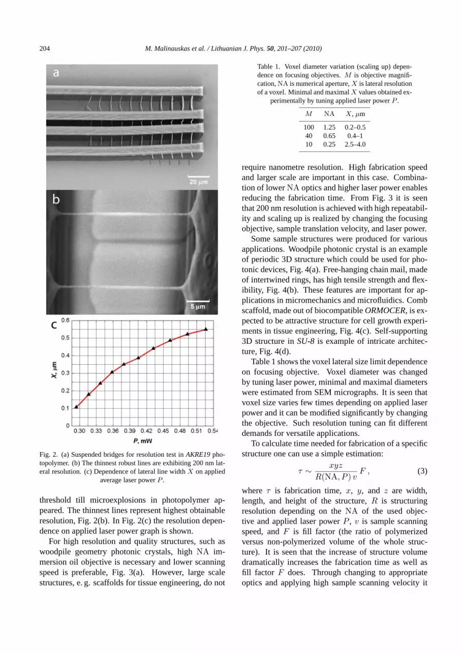
In our work, a novel LTPP prototype system hasbeen developed and tested for applications in mi-cro/nanostructuring. For resolution test inAKRE19the suspended bridge method was chosen [14]. Sus-pended lines hanging between solid supporting wallswere polymerized using highNA = 1.25 oil immer-sion microscope objective. Structure features were ex-amined by scanning electron microscopy (SEM). In thetest structure shown in Fig. 2(a), polymer lines werefabricated using the same scanning speed of 100µm/sand varying the laser power from below polymerization
204 M. Malinauskas et al. / Lithuanian J. Phys.50, 201–207 (2010)
Fig. 2. (a) Suspended bridges for resolution test inAKRE19pho-topolymer. (b) The thinnest robust lines are exhibiting 200 nm lat-eral resolution. (c) Dependence of lateral line widthX on applied
average laser powerP .
threshold till microexplosions in photopolymer ap-peared. The thinnest lines represent highest obtainableresolution, Fig. 2(b). In Fig. 2(c) the resolution depen-dence on applied laser power graph is shown.
For high resolution and quality structures, such aswoodpile geometry photonic crystals, highNA im-mersion oil objective is necessary and lower scanningspeed is preferable, Fig. 3(a). However, large scalestructures, e. g. scaffolds for tissue engineering, do not
Table 1. Voxel diameter variation (scaling up) depen-dence on focusing objectives.M is objective magnifi-cation,NA is numerical aperture,X is lateral resolutionof a voxel. Minimal and maximalX values obtained ex-
perimentally by tuning applied laser powerP .
M NA X, µm
100 1.25 0.2–0.540 0.65 0.4–110 0.25 2.5–4.0
require nanometre resolution. High fabrication speedand larger scale are important in this case. Combina-tion of lowerNA optics and higher laser power enablesreducing the fabrication time. From Fig. 3 it is seenthat 200 nm resolution is achieved with high repeatabil-ity and scaling up is realized by changing the focusingobjective, sample translation velocity, and laser power.
Some sample structures were produced for variousapplications. Woodpile photonic crystal is an exampleof periodic 3D structure which could be used for pho-tonic devices, Fig. 4(a). Free-hanging chain mail, madeof intertwined rings, has high tensile strength and flex-ibility, Fig. 4(b). These features are important for ap-plications in micromechanics and microfluidics. Combscaffold, made out of biocompatibleORMOCER, is ex-pected to be attractive structure for cell growth experi-ments in tissue engineering, Fig. 4(c). Self-supporting3D structure inSU-8 is example of intricate architec-ture, Fig. 4(d).
Table 1 shows the voxel lateral size limit dependenceon focusing objective. Voxel diameter was changedby tuning laser power, minimal and maximal diameterswere estimated from SEM micrographs. It is seen thatvoxel size varies few times depending on applied laserpower and it can be modified significantly by changingthe objective. Such resolution tuning can fit differentdemands for versatile applications.
To calculate time needed for fabrication of a specificstructure one can use a simple estimation:
τ ∼ xyz
R(NA, P ) vF , (3)
where τ is fabrication time,x, y, and z are width,length, and height of the structure,R is structuringresolution depending on theNA of the used objec-tive and applied laser powerP , v is sample scanningspeed, andF is fill factor (the ratio of polymerizedversus non-polymerized volume of the whole struc-ture). It is seen that the increase of structure volumedramatically increases the fabrication time as well asfill factor F does. Through changing to appropriateoptics and applying high sample scanning velocity it

M. Malinauskas et al. / Lithuanian J. Phys.50, 201–207 (2010) 205
Fig. 3. SEM images of grid structures produced inAKRE19photopolymer. Resolution, period, scanning speed, grid size, magnification,andNA of focusing objectives given, respectively: (a) 200 nm, 1µm, 100µm/s, 200×200µm2, 100×, 1.25, (b) 450 nm, 4µm, 1 mm/s,500×500µm2, 40×, 0.65, (c) 800 nm, 3µm, 10 mm/s, 500×500µm2, 40×, 0.65, (d) 3500 nm, 50µm, 100 mm/s, 1.5×1.5 cm2, 100×,
1.25.
Fig. 4. SEM images of sample structures from various materials. (a) Photonic crystal (woodpile structure) inAKRE19photopolymerwith 0.5 µm period and resolution 200 nm, structure size 40×40 µm2, fabrication time 15 min. (b) Free-hanging chain mail inAKRE19photopolymer, resolution 400 nm, structure size 80×80 µm2, fabrication time 15 min. (c) Comb scaffold for cell growth inORMOCER
hybrid photopolymer, structure size 4×4 mm2, fabrication time 30 min. (d) 3D structure inSU-8photoresist, fabrication time 20 min.
206 M. Malinauskas et al. / Lithuanian J. Phys.50, 201–207 (2010)
is possible to produce a relatively large in filled vol-ume structure in less time. For example, fabricationof woodpile structure with lateral and axial period of 8and 2µm, respectively, having overall structure size of800×800×40 µm3 and roughly 0.5 filling ratio, scan-ning the sample at 1000µm/s speed would take just25 min using aNA = 0.25 objective. UsingNA = 1.25it would take up to 7 h to fabricate an identical struc-ture. However, if huge volumes are needed to be poly-merized and high feature resolution is required, a so-phisticated strategy to overcome the drawback of time-consuming fabrication can be invoked. For instance,if a cantilever with a sharp tip is needed, the huge involume body of the cantilever can be fabricated usinga low NA objective and then the sharp tip can be fab-ricated with a highNA objective. This combinationenables fabrication of relatively large (mm in overallscale) volumetric structures with submicrometre fea-ture resolution.
Summarizing, our experiments show that the con-structed LTPP system is suitable for rapid micro/nano-patterning of various photoresins and photopolymerswhich is a requisite for diverse applications in growingdemand of miniature functional devices.
5. Conclusion
Nanostructuring for routine fabrication is a com-plex task. Fast and flexible production, high through-put, easy to operate system, and low maintenance cost,yet high resolution is needed for applications in indus-try. It is hard to compromise all these requirementsat once. High resolution usually correlates with lowfabrication speed and small processible area. On theother hand, modification of large area is hardly real-ized with nanometre resolution or controllable manner.A novel LTPP system, based on high speed wide scan-ning area linear motor driven stages and high repeti-tion rate Yb:KGW VIS spectral range amplified laser,is offered as a solution. It enables rapid and flexiblefabrication of structures with a few hundred nanome-tres resolution. Furthermore, femtosecond green lightcapacitates one to produce 3D structures in most ofthe common photoresins. This sums up the systemto be a powerful nanotechnology tool for science andindustrial demands. The fabricated sample structuresshow possible applications in photonics, microoptics,micromechanics, microbiology, and tissue engineering.Though this 3D micro/nanostructuring approach seemsa promising prototype for mass production, it still canbe further upgraded. The excess of laser power can be
used for parallel beam processing in order to increasethe fabrication throughput. An integration of additionalOPA (optical parametric amplifier) would provide ir-radiation wavelength tuning from UV to NIR, whichwould extend the variety of processible materials andfabrication efficiency. Techniques for two-colour pro-cessing could lead to collateral increase of fabricationresolution as well.
Acknowledgements
This work is supported by the Lithuanian StateScience and Studies Foundation grant B09/08 (LaserMicro-processing With High Repetition FemtosecondPulses – FEMTOPROCESSING). In addition, authorswould like to thankSartomer Company, Inc.for pro-viding materials for the experiments. Lastly, authorsare grateful to Dr. A. Ovsianikov (NanotechnologyDepartment, Laser Zentrum Hannover, Hannover, Ger-many) for fruitful discussions.
References
[1] S. Wu, J. Serbin, and M. Gu, Two-photon polymeri-sation for three-dimensional micro-fabrication, J. Pho-tochem. Photobiol. A181(1), 1–11 (2006).
[2] S.H. Park, K.H. Kim, T.W. Lim, D.Y. Yang, andK.S. Lee, Investigation of three-dimensional patterncollapse owing to surface tension using an imperfec-tion finite element model, Microelectron. Eng.85,432–439 (2008).
[3] S. Kawata, H.B. Sun, T. Tanaka, and K. Takada, Finerfeatures for functional microdevices, Nature412, 697–698 (2001).
[4] S. Juodkazis, V. Mizeikis, K.K. Seet, M. Mima,and H. Misawa, Two-photon lithography of nanorodsin SU-8 photoresist, Nanotechnology16, 846–849(2005).
[5] B.N. Chichkov, J. Koch, A. Ovsianikov, S. Passinger,C. Reinhardt, and J. Serbin, Direct-write micro- andnanostructuring with femtosecond lasers, Mater. Res.Soc. Symp. Proc.850, 251–258 (2005).
[6] L. Li and J.T. Fourkas, Multiphoton polymerization,Mater. Today10(6), 30–37 (2007).
[7] W. Haske, V.W. Chen, J.M. Hales, W. Dong, S. Barlow,S.R. Marder, and J.W. Perry, 65 nm feature sizes usingvisible wavelength 3-D multiphoton lithography, Opt.Express15(6), 3426–3436 (2007).
[8] M. Farsari, G. Filippidis, and C. Fotakis, Fabricationof three-dimensional structures by three-photon poly-merization, Opt. Lett.30(23), 3180–3182 (2005).
[9] K.-S. Lee, R.H. Kim, D.-Y. Yang, and S.H. Park, Ad-vances in 3D nano/micro-fabrication using two-photon

M. Malinauskas et al. / Lithuanian J. Phys.50, 201–207 (2010) 207
initiated polymerization, Progr. Polymer Sci.33, 631–
681 (2008).
[10] www.sartomer.com/proddetail.asp?plid=1&sgid=4&
prid=SR368 (2008-07-09).
[11] www.sigmaaldrich.com/Area_of_Interest/Chemistry/
Materials_Science/Polymerization_Tools/
Initiators.html (2008-07-10).
[12] www.microresist.de/poster_ormocer.pdf(2006-05-13).
[13] www.microchem.com/products/pdf/SU8_2002-2025.pdf (2007-05-04).
[14] H.B. Sun and S. Kawata, Two-photon photopolymer-ization and 3D lithographic microfabrication, in:NMR.3D Analysis. Photopolymerization, Adv. Polymer Sci.170, 169–273 (2004).
FEMTOSEKUNDINIAIS REGIMOSIOS ŠVIESOS IMPULSAIS INDUKUOTOS DVIFOTON ESPOLIMERIZACIJOS PANAUDOJIMAS TRIMA CIAMS MIKRO- AR NANODARINIAMS FORMUOTI
FOTOREZISTUOSE IR FOTOPOLIMERUOSE
M. Malinauskas, V. Purlys, M. Rutkauskas, A. Gaidukevici ute, R. Gadonas
Vilniaus universitetas, Vilnius, Lietuva
Santrauka
Lazerine dvifotone fotopolimerizacija (LDFP) – unikali techno-logija, naudojama trimaciam mikro- ar nanostrukt urizavimui. Toksfemtosekundiniais lazeriais paremtas tiesioginis rašymas leidžiapasiekti mažesne už bangos ilgi objektu formavimo skyra. Pri-statoma sukonstruota LDFP sistema, panaudojant didelio darbiniolauko (150×150×4 mm3) ir skenavimo greicio (iki 300 mm/s)bandinio pozicionavimo stalus ir aukšto pasikartojimo dažnio(312,5 kHz) Yb:KGW lazerio spinduliuotes antraja harmonika(515 nm) kaip šviesos šaltini. Ja sparciai ir atkartojamai galima for-
muoti nanodarinius 200 nm skersine skyra. Keiciant lazerio pluoštofokusavimo optika, galima derinti ir optimizuoti tokio formavimotiksluma bei našuma. Tai leidžia gaminti milimetriniu matmenutrimacius darinius, kurie gali b uti taikomi mikrooptikoje, fotoni-koje, mikrohidrodinamikoje, audiniu inžinerijoje ir kitur. Tam ga-lima naudoti ivairias UV litografijoje naudojamas fotojautrias me-džiagas (akrilatus, hibridinius organinius–neorganinius polimerus,epoksidines dervas). Visa tai leidžia sukurta LDFP sistema efek-tyviai naudoti sparciam ir lanksciam palyginus dideliu matmenumikro- ar nanodariniu formavimui.


![Plasma-surface interactions of model polymers for advanced photoresists using C[sub 4]F[sub 8]∕Ar discharges and energetic ion beams](https://img.pdfslide.net/doc/110x75/634fb209eb6c0295f803f208/plasma-surface-interactions-of-model-polymers-for-advanced-photoresists-using-csub.jpg)


