Embed Size (px)
Citation preview
ARTICLE IN PRESS
0927-0248/$ - se
doi:10.1016/j.so
�CorrespondE-mail addr
Solar Energy Materials & Solar Cells 91 (2007) 572–580
www.elsevier.com/locate/solmat
Flexible amorphous and microcrystalline silicon tandem solar modulesin the temporary superstrate concept
M.N. van den Donkera,�, A. Gordijna, H. Stiebiga, F. Fingera, B. Recha, B. Stannowskib,R. Bartlb, E.A.G. Hamersb, R. Schlatmannb, G.J. Jongerdenb
aInstitute of Photovoltaics, Forschungszentrum Juelich GmbH, 52425 Julich, GermanybHelianthos B.V., P.O. Box 9300, 6800 SB, Arnhem, The Netherlands
Received 18 July 2006; accepted 15 November 2006
Available online 16 January 2007
Abstract
Encapsulated and series-connected amorphous silicon (a-Si:H) and microcrystalline silicon (mc-Si:H) based thin film silicon solar
modules were developed in the superstrate configuration using an aluminum foil as temporary substrate during processing and a
commodity polymer as permanent substrate in the finished module. For the development of mc-Si:H single junction modules, aspects
regarding TCO conductivity, TCO reduction, deposition uniformity, substrate temperature stability and surface morphology were
addressed. It was established that on sharp TCO morphologies where single junction mc-Si:H solar cells fail, tandem structures consisting
of an a-Si:H top cell and a mc-Si:H bottom cell can still show a good performance. Initial aperture area efficiencies of 8.2%, 3.9% and
9.4% were obtained for fully encapsulated amorphous silicon (a-Si:H) single junction, microcrystalline silicon (mc-Si:H) single junction
and a-Si:H/mc-Si:H tandem junction modules, respectively.
r 2006 Elsevier B.V. All rights reserved.
Keywords: Flexible; Thin-film silicon; Photovoltaic modules
1. Introduction
Thin film silicon solar cells are one of the most promisingoptions for providing clean and cost-effective solarelectricity. Tandem junctions consisting of an amorphoussilicon (a-Si:H) top cell and a microcrystalline silicon (mc-Si:H) bottom cell are of particular interest since by thisconcept stable solar energy conversion efficiencies of cellsand modules well above 10% have been demonstrated[1–6]. It remains an important challenge to transfer theproven lab-scale technology on glass to more cost-effectiveprocesses and materials. One route is up-scaling the glasstechnology to �m2 size and beyond [3,5,7]. Anotherpossible route is to use flexible substrate foils in combina-tion with roll-to-roll deposition technology.
Thin film silicon solar cells on glass are typicallyfabricated in the superstrate configuration, in which light
e front matter r 2006 Elsevier B.V. All rights reserved.
lmat.2006.11.012
ing author. Tel.: +49 2461 61 4855; fax: +49 2461 61 3735.
ess: [email protected] (M.N. van den Donker).
enters the solar cell through the glass substrate. For asuccessful realization of flexible solar cells in this super-strate configuration the substrate foil would have to fulfillthe three main requirements of (i) optical transparency, (ii)temperature compatibility and (iii) cost-effectiveness.Lambertz et al. investigated to what degree polycarbonatecould fulfill these requirements and realized an efficiency of4.9% for an a-Si:H single junction solar cell [8].An approach to relax on the transparency requirement is
to use the substrate configuration. In this configuration thesolar cell is deposited on a reflecting substrate and suppliedwith a transparent front contact (typically In2O3:Sn)afterwards. Using this substrate configuration, the AISTresearch centre realized an initial solar energy conversionefficiency of 6% for a small area single junction mc-Si:Hsolar cell on a polymer substrate foil [9]. The IMTNeuchatel also used a polymer substrate foil and obtaineda stabilized solar energy conversion efficiency of 7% for asingle junction a-Si:H solar cell and 8.3% for a small-areatandem junction a-Si:H/mc-Si:H solar cell [10]. Fuji Electric
ARTICLE IN PRESSM.N. van den Donker et al. / Solar Energy Materials & Solar Cells 91 (2007) 572–580 573
Corp. developed a roll-to-roll process on a polymersubstrate foil, and reported on 9% stable efficiency for0.12m2 cells using an a-Si:H/amorphous silicon–germa-nium (a-SiGe:H) tandem junction [11]. United SolarOvonic Corp. developed a roll-to-roll process on a stainlesssteel substrate foil [12], and reported various recordperformances (�13% stable efficiency) for individualsmall-area triple junction solar cells based on a-Si:H, a-SiGe:H and mc-Si:H [4,13,14]. In addition to the researchreviewed above, companies like PowerFilm (USA) andVHF Technologies (Switzerland) work on the commercia-lization of flexible solar cells in the substrate configuration.A challenge for this flexible substrate configuration is tofind cost-effective low-temperature compatible transparentfront contacts and to develop methods of monolithicalseries connection.
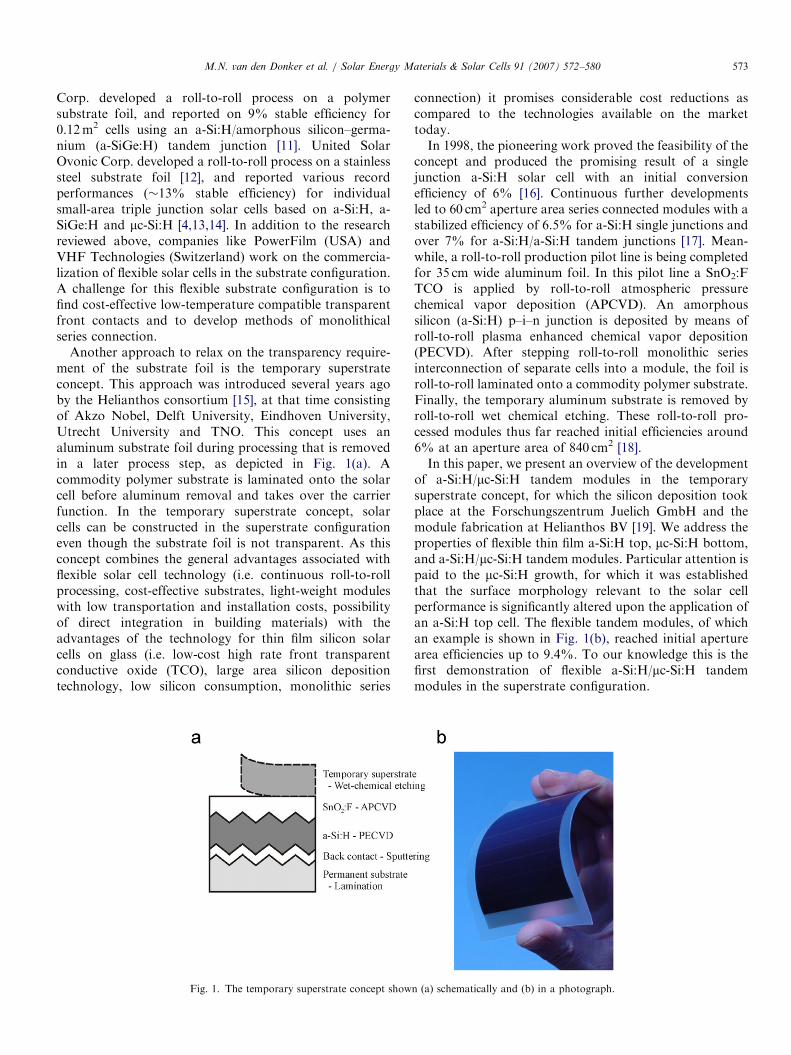
Another approach to relax on the transparency require-ment of the substrate foil is the temporary superstrateconcept. This approach was introduced several years agoby the Helianthos consortium [15], at that time consistingof Akzo Nobel, Delft University, Eindhoven University,Utrecht University and TNO. This concept uses analuminum substrate foil during processing that is removedin a later process step, as depicted in Fig. 1(a). Acommodity polymer substrate is laminated onto the solarcell before aluminum removal and takes over the carrierfunction. In the temporary superstrate concept, solarcells can be constructed in the superstrate configurationeven though the substrate foil is not transparent. As thisconcept combines the general advantages associated withflexible solar cell technology (i.e. continuous roll-to-rollprocessing, cost-effective substrates, light-weight moduleswith low transportation and installation costs, possibilityof direct integration in building materials) with theadvantages of the technology for thin film silicon solarcells on glass (i.e. low-cost high rate front transparentconductive oxide (TCO), large area silicon depositiontechnology, low silicon consumption, monolithic series
Fig. 1. The temporary superstrate concept show
connection) it promises considerable cost reductions ascompared to the technologies available on the markettoday.In 1998, the pioneering work proved the feasibility of the
concept and produced the promising result of a singlejunction a-Si:H solar cell with an initial conversionefficiency of 6% [16]. Continuous further developmentsled to 60 cm2 aperture area series connected modules with astabilized efficiency of 6.5% for a-Si:H single junctions andover 7% for a-Si:H/a-Si:H tandem junctions [17]. Mean-while, a roll-to-roll production pilot line is being completedfor 35 cm wide aluminum foil. In this pilot line a SnO2:FTCO is applied by roll-to-roll atmospheric pressurechemical vapor deposition (APCVD). An amorphoussilicon (a-Si:H) p–i–n junction is deposited by means ofroll-to-roll plasma enhanced chemical vapor deposition(PECVD). After stepping roll-to-roll monolithic seriesinterconnection of separate cells into a module, the foil isroll-to-roll laminated onto a commodity polymer substrate.Finally, the temporary aluminum substrate is removed byroll-to-roll wet chemical etching. These roll-to-roll pro-cessed modules thus far reached initial efficiencies around6% at an aperture area of 840 cm2 [18].In this paper, we present an overview of the development
of a-Si:H/mc-Si:H tandem modules in the temporarysuperstrate concept, for which the silicon deposition tookplace at the Forschungszentrum Juelich GmbH and themodule fabrication at Helianthos BV [19]. We address theproperties of flexible thin film a-Si:H top, mc-Si:H bottom,and a-Si:H/mc-Si:H tandem modules. Particular attention ispaid to the mc-Si:H growth, for which it was establishedthat the surface morphology relevant to the solar cellperformance is significantly altered upon the application ofan a-Si:H top cell. The flexible tandem modules, of whichan example is shown in Fig. 1(b), reached initial aperturearea efficiencies up to 9.4%. To our knowledge this is thefirst demonstration of flexible a-Si:H/mc-Si:H tandemmodules in the superstrate configuration.
n (a) schematically and (b) in a photograph.
ARTICLE IN PRESSM.N. van den Donker et al. / Solar Energy Materials & Solar Cells 91 (2007) 572–580574
2. Experimental details
The configuration of the flexible solar cells is sketched inFig. 1(a). Starting from an aluminum foil, all layers—TCOfront contact, silicon p–i–n solar cell, ZnO/Al backcontact, and permanent substrate—were subsequentlyapplied. As last step, the aluminum foil was removed in awet-chemical etching process, opening up the solar cell tolight. In some reference experiments the TCO, p–i–n, andback contact were applied on glass.
On the flexible foil the SnO2:F was deposited in a roll-to-roll APCVD process [15,20]. Tin-tetra-chloride (TTC) wasused as tin precursor and HF as doping gas. Pieces of10� 10 cm2 were later cut out of the roll of foil. Forcomparison with cells on glass commercially availableSnO2:F (Asahi U-type) and texture-etched magnetronsputtered ZnO:Al [5,21,22] was used. The silicon p–i–nstructures were deposited in a 30� 30 cm2 parallel platePECVD reactor described in detail elsewhere [23]. Thissystem consisted of one load lock and two depositionchambers, both equipped with showerhead electrodes forhomogeneous gas distribution. Deposition took place fromSiH4 and H2 source gases using 13.56MHz excitationfrequency, for the mc-Si:H in a regime of high pressure andhigh power yielding rates of 0.5 nm s�1 [24]. Doped layerswere obtained by admixture of either B(CH3)3 (p-layer) orPH3 (n-layer). Up to four 10� 10 cm2 substrates could befitted at the same time in the 30� 30 cm2 substrate carrier.In a single experiment mentioned specifically in Section 3.3we used a 10� 10 cm2 reactor equipped with a pyrometer[25] to study the substrate temperature during deposition.Sputtered ZnO/Al was used as back contact on the flexiblesamples. Cells were defined by a laser scribe patterningprocess. Eight cells made up one module. Reference cellson glass were provided with evaporated Ag or sputteredZnO/Ag back contacts.
The TCO was characterized by atomic force microscopy(AFM), scanning electron microscopy (SEM) and Hallmeasurements. The electrical characterization was possibleby laminating the TCO on the commodity polymer andetching away the conducting aluminium.
The solar cells and modules were characterized bycurrent–voltage (J–V) measurements. A double sourceclass A DC solar simulator was used next to a flasher. Inpreceding work the DC solar simulator and the flasherwere found to differ less than 2% relative from each otherand from independent reference measurements at NREL[26]. In each characterization we checked whether theresults of the two solar simulators were in agreement. If notspecifically stated otherwise, the results obtained with theDC simulator will be mentioned. Illuminated J–V char-acterization (AM 1.5, 100mW/cm2, 25 1C) yielded theparameters of solar energy conversion efficiency (Z), fillfactor (FF), open-circuit voltage (Voc), short-circuit currentdensity (Jsc), open-circuit resistance (Roc) and short-circuitresistance (Rsc). Dark J–V characterization yielded theparameters diode ideality factor (n), reverse bias saturation
current density (J0), series resistance (Rs) and parallelresistance (Rp). To be able to compare module and cellresults the voltage of the modules was divided by thenumber of cells in a module and is expressed in the unit V/cell. The current of the modules was multiplied by thenumber of cells and divided by the module aperture areaand is expressed in the unit mA/cm2. Similarly, theresistance is expressed in the unit O cm2.External quantum efficiency (EQE) measurements were
performed on some modules. The AC probe beam had adiameter larger than the module size so that the entiremodule could be probed. Red and blue bias light wasapplied to measure the EQE of the top- and bottom cellseparately. Light soaking of the a-Si:H/mc-Si:H tandemmodules was carried out at 50 1C, AM 1.5, 100mW/cm2
under open-circuit conditions.
3. Results: tandem development
3.1. Substrates
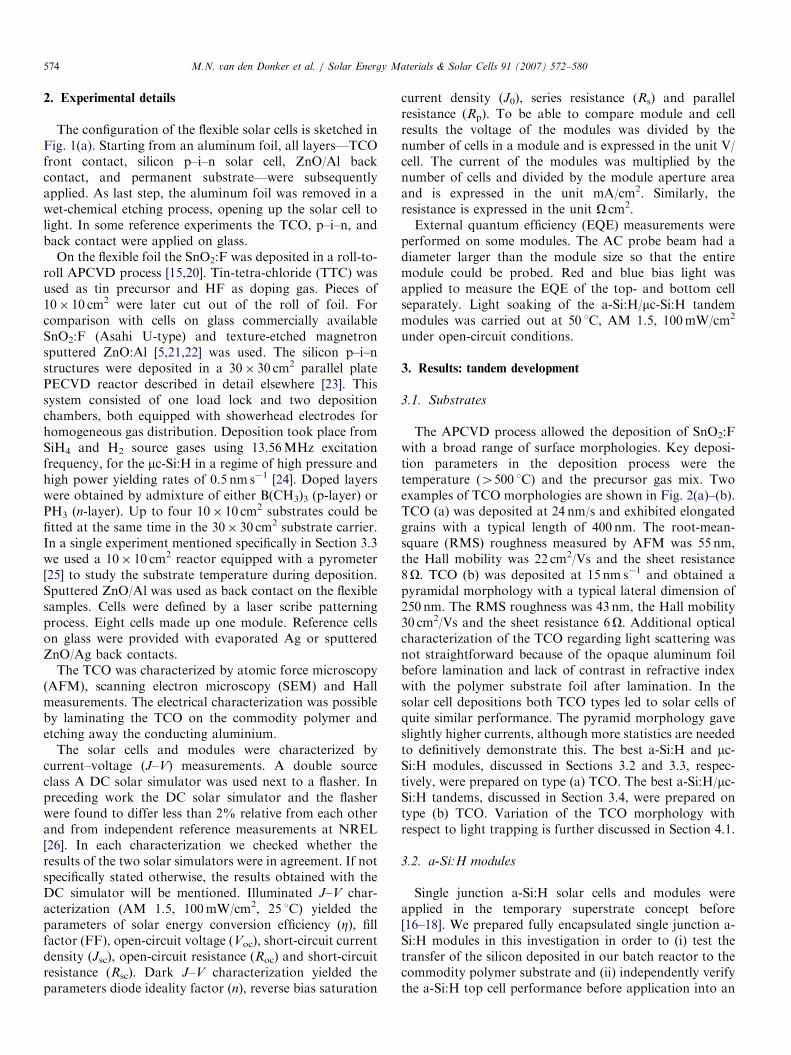
The APCVD process allowed the deposition of SnO2:Fwith a broad range of surface morphologies. Key deposi-tion parameters in the deposition process were thetemperature (4500 1C) and the precursor gas mix. Twoexamples of TCO morphologies are shown in Fig. 2(a)–(b).TCO (a) was deposited at 24 nm/s and exhibited elongatedgrains with a typical length of 400 nm. The root-mean-square (RMS) roughness measured by AFM was 55 nm,the Hall mobility was 22 cm2/Vs and the sheet resistance8O. TCO (b) was deposited at 15 nm s�1 and obtained apyramidal morphology with a typical lateral dimension of250 nm. The RMS roughness was 43 nm, the Hall mobility30 cm2/Vs and the sheet resistance 6O. Additional opticalcharacterization of the TCO regarding light scattering wasnot straightforward because of the opaque aluminum foilbefore lamination and lack of contrast in refractive indexwith the polymer substrate foil after lamination. In thesolar cell depositions both TCO types led to solar cells ofquite similar performance. The pyramid morphology gaveslightly higher currents, although more statistics are neededto definitively demonstrate this. The best a-Si:H and mc-Si:H modules, discussed in Sections 3.2 and 3.3, respec-tively, were prepared on type (a) TCO. The best a-Si:H/mc-Si:H tandems, discussed in Section 3.4, were prepared ontype (b) TCO. Variation of the TCO morphology withrespect to light trapping is further discussed in Section 4.1.
3.2. a-Si:H modules
Single junction a-Si:H solar cells and modules wereapplied in the temporary superstrate concept before[16–18]. We prepared fully encapsulated single junction a-Si:H modules in this investigation in order to (i) test thetransfer of the silicon deposited in our batch reactor to thecommodity polymer substrate and (ii) independently verifythe a-Si:H top cell performance before application into an
ARTICLE IN PRESS
Fig. 2. Scanning electron microscope (SEM) images of two types of roll-
to-roll SnO2:F TCOs on aluminum foil: (a) elongated grain structure and
(b) pyramid structure.
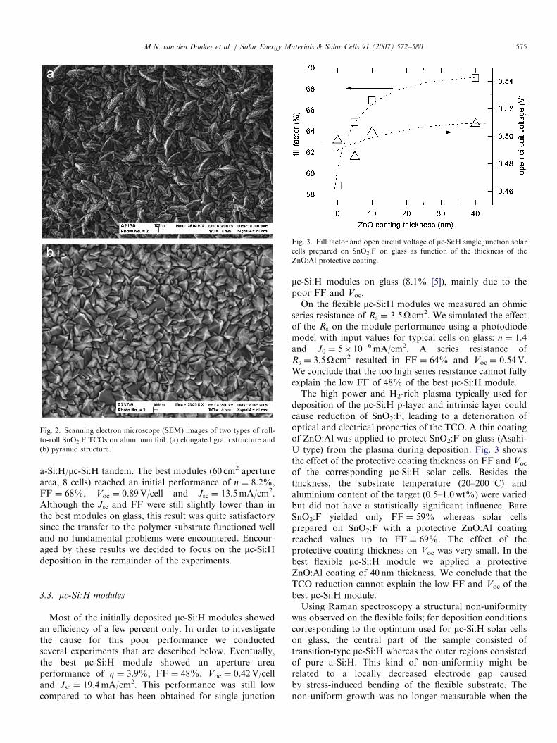
Fig. 3. Fill factor and open circuit voltage of mc-Si:H single junction solar
cells prepared on SnO2:F on glass as function of the thickness of the
ZnO:Al protective coating.
M.N. van den Donker et al. / Solar Energy Materials & Solar Cells 91 (2007) 572–580 575
a-Si:H/mc-Si:H tandem. The best modules (60 cm2 aperturearea, 8 cells) reached an initial performance of Z ¼ 8.2%,FF ¼ 68%, Voc ¼ 0.89V/cell and Jsc ¼ 13.5mA/cm2.Although the Jsc and FF were still slightly lower than inthe best modules on glass, this result was quite satisfactorysince the transfer to the polymer substrate functioned welland no fundamental problems were encountered. Encour-aged by these results we decided to focus on the mc-Si:Hdeposition in the remainder of the experiments.
3.3. mc-Si:H modules
Most of the initially deposited mc-Si:H modules showedan efficiency of a few percent only. In order to investigatethe cause for this poor performance we conductedseveral experiments that are described below. Eventually,the best mc-Si:H module showed an aperture areaperformance of Z ¼ 3.9%, FF ¼ 48%, Voc ¼ 0.42V/celland Jsc ¼ 19.4mA/cm2. This performance was still lowcompared to what has been obtained for single junction
mc-Si:H modules on glass (8.1% [5]), mainly due to thepoor FF and Voc.On the flexible mc-Si:H modules we measured an ohmic
series resistance of Rs ¼ 3.5O cm2. We simulated the effectof the Rs on the module performance using a photodiodemodel with input values for typical cells on glass: n ¼ 1.4and J0 ¼ 5� 10�6mA/cm2. A series resistance ofRs ¼ 3.5O cm2 resulted in FF ¼ 64% and Voc ¼ 0.54V.We conclude that the too high series resistance cannot fullyexplain the low FF of 48% of the best mc-Si:H module.The high power and H2-rich plasma typically used for
deposition of the mc-Si:H p-layer and intrinsic layer couldcause reduction of SnO2:F, leading to a deterioration ofoptical and electrical properties of the TCO. A thin coatingof ZnO:Al was applied to protect SnO2:F on glass (Asahi-U type) from the plasma during deposition. Fig. 3 showsthe effect of the protective coating thickness on FF and Voc
of the corresponding mc-Si:H solar cells. Besides thethickness, the substrate temperature (20–200 1C) andaluminium content of the target (0.5–1.0wt%) were variedbut did not have a statistically significant influence. BareSnO2:F yielded only FF ¼ 59% whereas solar cellsprepared on SnO2:F with a protective ZnO:Al coatingreached values up to FF ¼ 69%. The effect of theprotective coating thickness on Voc was very small. In thebest flexible mc-Si:H module we applied a protectiveZnO:Al coating of 40 nm thickness. We conclude that theTCO reduction cannot explain the low FF and Voc of thebest mc-Si:H module.Using Raman spectroscopy a structural non-uniformity
was observed on the flexible foils; for deposition conditionscorresponding to the optimum used for mc-Si:H solar cellson glass, the central part of the sample consisted oftransition-type mc-Si:H whereas the outer regions consistedof pure a-Si:H. This kind of non-uniformity might berelated to a locally decreased electrode gap causedby stress-induced bending of the flexible substrate. Thenon-uniform growth was no longer measurable when the
ARTICLE IN PRESSM.N. van den Donker et al. / Solar Energy Materials & Solar Cells 91 (2007) 572–580576
SiH4 flow was decreased by �5%. Such a small decrease ofthe SiH4 flow is expected to affect Voc and FF onlymarginally [2,24]. We conclude that this non-uniformgrowth and the resulting adaptation of the depositionregime for flexible substrates cannot fully explain the lowFF and Voc of the best mc-Si:H module.
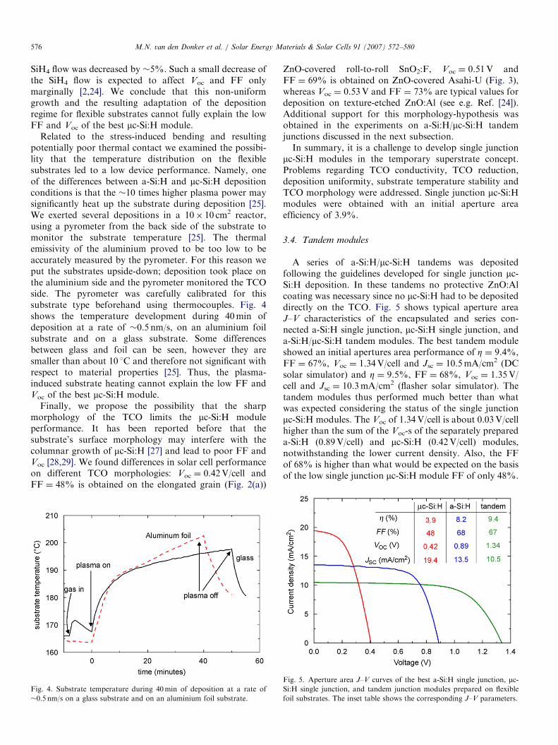
Related to the stress-induced bending and resultingpotentially poor thermal contact we examined the possibi-lity that the temperature distribution on the flexiblesubstrates led to a low device performance. Namely, oneof the differences between a-Si:H and mc-Si:H depositionconditions is that the �10 times higher plasma power maysignificantly heat up the substrate during deposition [25].We exerted several depositions in a 10� 10 cm2 reactor,using a pyrometer from the back side of the substrate tomonitor the substrate temperature [25]. The thermalemissivity of the aluminium proved to be too low to beaccurately measured by the pyrometer. For this reason weput the substrates upside-down; deposition took place onthe aluminium side and the pyrometer monitored the TCOside. The pyrometer was carefully calibrated for thissubstrate type beforehand using thermocouples. Fig. 4shows the temperature development during 40min ofdeposition at a rate of �0.5 nm/s, on an aluminium foilsubstrate and on a glass substrate. Some differencesbetween glass and foil can be seen, however they aresmaller than about 10 1C and therefore not significant withrespect to material properties [25]. Thus, the plasma-induced substrate heating cannot explain the low FF andVoc of the best mc-Si:H module.
Finally, we propose the possibility that the sharpmorphology of the TCO limits the mc-Si:H moduleperformance. It has been reported before that thesubstrate’s surface morphology may interfere with thecolumnar growth of mc-Si:H [27] and lead to poor FF andVoc [28,29]. We found differences in solar cell performanceon different TCO morphologies: Voc ¼ 0.42V/cell andFF ¼ 48% is obtained on the elongated grain (Fig. 2(a))
Fig. 4. Substrate temperature during 40min of deposition at a rate of
�0.5 nm/s on a glass substrate and on an aluminium foil substrate.
ZnO-covered roll-to-roll SnO2:F, Voc ¼ 0.51V andFF ¼ 69% is obtained on ZnO-covered Asahi-U (Fig. 3),whereas Voc ¼ 0.53V and FF ¼ 73% are typical values fordeposition on texture-etched ZnO:Al (see e.g. Ref. [24]).Additional support for this morphology-hypothesis wasobtained in the experiments on a-Si:H/mc-Si:H tandemjunctions discussed in the next subsection.In summary, it is a challenge to develop single junction
mc-Si:H modules in the temporary superstrate concept.Problems regarding TCO conductivity, TCO reduction,deposition uniformity, substrate temperature stability andTCO morphology were addressed. Single junction mc-Si:Hmodules were obtained with an initial aperture areaefficiency of 3.9%.
3.4. Tandem modules
A series of a-Si:H/mc-Si:H tandems was depositedfollowing the guidelines developed for single junction mc-Si:H deposition. In these tandems no protective ZnO:Alcoating was necessary since no mc-Si:H had to be depositeddirectly on the TCO. Fig. 5 shows typical aperture areaJ–V characteristics of the encapsulated and series con-nected a-Si:H single junction, mc-Si:H single junction, anda-Si:H/mc-Si:H tandem modules. The best tandem moduleshowed an initial apertures area performance of Z ¼ 9.4%,FF ¼ 67%, Voc ¼ 1.34V/cell and Jsc ¼ 10.5mA/cm2 (DCsolar simulator) and Z ¼ 9.5%, FF ¼ 68%, Voc ¼ 1.35V/cell and Jsc ¼ 10.3mA/cm2 (flasher solar simulator). Thetandem modules thus performed much better than whatwas expected considering the status of the single junctionmc-Si:H modules. The Voc of 1.34V/cell is about 0.03V/cellhigher than the sum of the Voc-s of the separately prepareda-Si:H (0.89V/cell) and mc-Si:H (0.42V/cell) modules,notwithstanding the lower current density. Also, the FFof 68% is higher than what would be expected on the basisof the low single junction mc-Si:H module FF of only 48%.
Fig. 5. Aperture area J–V curves of the best a-Si:H single junction, mc-Si:H single junction, and tandem junction modules prepared on flexible
foil substrates. The inset table shows the corresponding J–V parameters.
ARTICLE IN PRESSM.N. van den Donker et al. / Solar Energy Materials & Solar Cells 91 (2007) 572–580 577
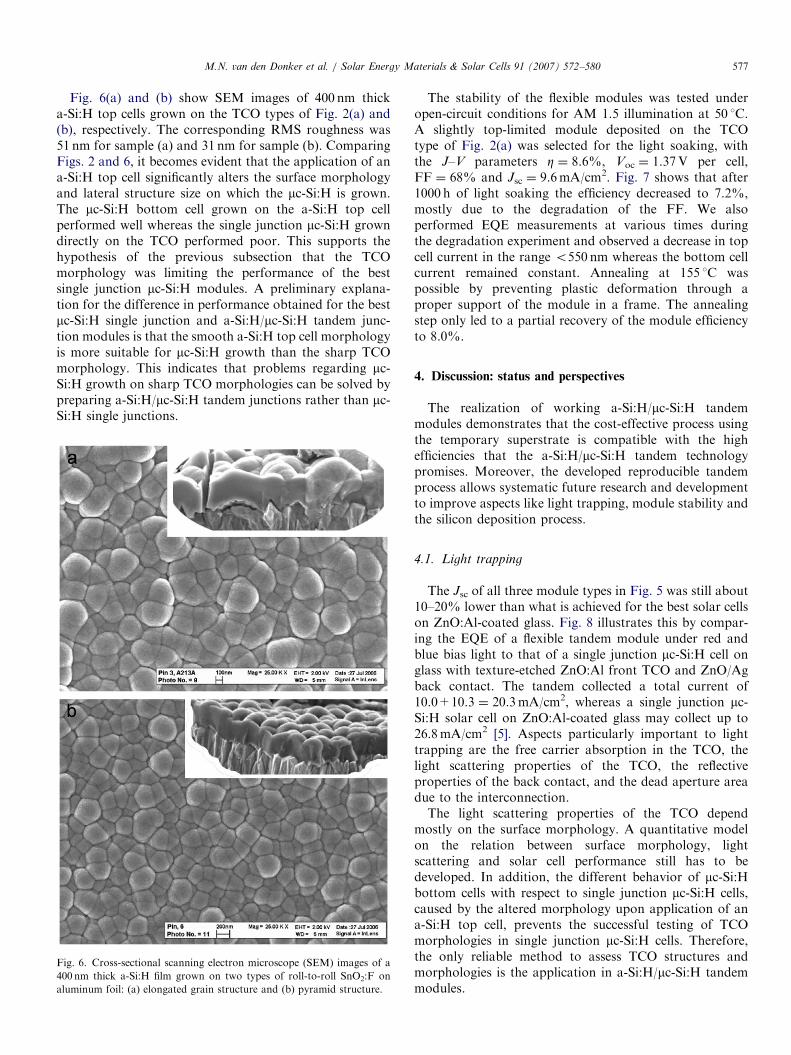
Fig. 6(a) and (b) show SEM images of 400 nm thicka-Si:H top cells grown on the TCO types of Fig. 2(a) and(b), respectively. The corresponding RMS roughness was51 nm for sample (a) and 31 nm for sample (b). ComparingFigs. 2 and 6, it becomes evident that the application of ana-Si:H top cell significantly alters the surface morphologyand lateral structure size on which the mc-Si:H is grown.The mc-Si:H bottom cell grown on the a-Si:H top cellperformed well whereas the single junction mc-Si:H growndirectly on the TCO performed poor. This supports thehypothesis of the previous subsection that the TCOmorphology was limiting the performance of the bestsingle junction mc-Si:H modules. A preliminary explana-tion for the difference in performance obtained for the bestmc-Si:H single junction and a-Si:H/mc-Si:H tandem junc-tion modules is that the smooth a-Si:H top cell morphologyis more suitable for mc-Si:H growth than the sharp TCOmorphology. This indicates that problems regarding mc-Si:H growth on sharp TCO morphologies can be solved bypreparing a-Si:H/mc-Si:H tandem junctions rather than mc-Si:H single junctions.
Fig. 6. Cross-sectional scanning electron microscope (SEM) images of a
400 nm thick a-Si:H film grown on two types of roll-to-roll SnO2:F on
aluminum foil: (a) elongated grain structure and (b) pyramid structure.
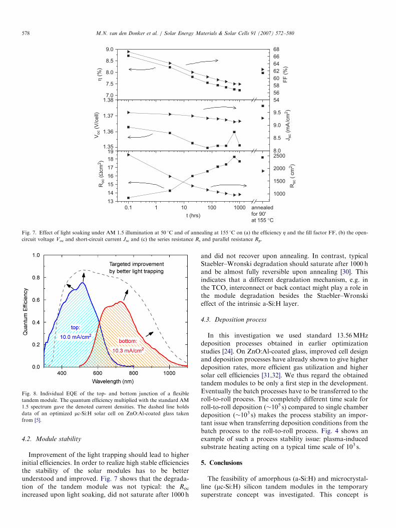
The stability of the flexible modules was tested underopen-circuit conditions for AM 1.5 illumination at 50 1C.A slightly top-limited module deposited on the TCOtype of Fig. 2(a) was selected for the light soaking, withthe J–V parameters Z ¼ 8.6%, Voc ¼ 1.37V per cell,FF ¼ 68% and Jsc ¼ 9.6mA/cm2. Fig. 7 shows that after1000 h of light soaking the efficiency decreased to 7.2%,mostly due to the degradation of the FF. We alsoperformed EQE measurements at various times duringthe degradation experiment and observed a decrease in topcell current in the range o550 nm whereas the bottom cellcurrent remained constant. Annealing at 155 1C waspossible by preventing plastic deformation through aproper support of the module in a frame. The annealingstep only led to a partial recovery of the module efficiencyto 8.0%.
4. Discussion: status and perspectives
The realization of working a-Si:H/mc-Si:H tandemmodules demonstrates that the cost-effective process usingthe temporary superstrate is compatible with the highefficiencies that the a-Si:H/mc-Si:H tandem technologypromises. Moreover, the developed reproducible tandemprocess allows systematic future research and developmentto improve aspects like light trapping, module stability andthe silicon deposition process.
4.1. Light trapping
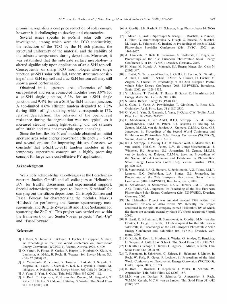
The Jsc of all three module types in Fig. 5 was still about10–20% lower than what is achieved for the best solar cellson ZnO:Al-coated glass. Fig. 8 illustrates this by compar-ing the EQE of a flexible tandem module under red andblue bias light to that of a single junction mc-Si:H cell onglass with texture-etched ZnO:Al front TCO and ZnO/Agback contact. The tandem collected a total current of10.0+10.3 ¼ 20.3mA/cm2, whereas a single junction mc-Si:H solar cell on ZnO:Al-coated glass may collect up to26.8mA/cm2 [5]. Aspects particularly important to lighttrapping are the free carrier absorption in the TCO, thelight scattering properties of the TCO, the reflectiveproperties of the back contact, and the dead aperture areadue to the interconnection.The light scattering properties of the TCO depend
mostly on the surface morphology. A quantitative modelon the relation between surface morphology, lightscattering and solar cell performance still has to bedeveloped. In addition, the different behavior of mc-Si:Hbottom cells with respect to single junction mc-Si:H cells,caused by the altered morphology upon application of ana-Si:H top cell, prevents the successful testing of TCOmorphologies in single junction mc-Si:H cells. Therefore,the only reliable method to assess TCO structures andmorphologies is the application in a-Si:H/mc-Si:H tandemmodules.
ARTICLE IN PRESS
0.1 1 10 100 100013
14
15
16
17
18
19
1000
1500
2000
2500
1.35
1.36
1.37
1.38
8.0
8.5
9.0
9.5
7.0
7.5
8.0
8.5
9.0
54
56
58
60
62
64
66
68
Roc (
Ωcm
2)
t (hrs)
Rsc (
cm
2)
annealed
for 90'
at 155 °C
Voc (
V/c
ell)
Jsc (
mA
/cm
2)
η (%
)
FF
(%
)
Fig. 7. Effect of light soaking under AM 1.5 illumination at 50 1C and of annealing at 155 1C on (a) the efficiency Z and the fill factor FF, (b) the open-
circuit voltage Voc and short-circuit current Jsc and (c) the series resistance Rs and parallel resistance Rp.
Fig. 8. Individual EQE of the top- and bottom junction of a flexible
tandem module. The quantum efficiency multiplied with the standard AM
1.5 spectrum gave the denoted current densities. The dashed line holds
data of an optimized mc-Si:H solar cell on ZnO:Al-coated glass taken
from [5].
M.N. van den Donker et al. / Solar Energy Materials & Solar Cells 91 (2007) 572–580578
4.2. Module stability
Improvement of the light trapping should lead to higherinitial efficiencies. In order to realize high stable efficienciesthe stability of the solar modules has to be betterunderstood and improved. Fig. 7 shows that the degrada-tion of the tandem module was not typical: the Roc
increased upon light soaking, did not saturate after 1000 h
and did not recover upon annealing. In contrast, typicalStaebler–Wronski degradation should saturate after 1000 hand be almost fully reversible upon annealing [30]. Thisindicates that a different degradation mechanism, e.g. inthe TCO, interconnect or back contact might play a role inthe module degradation besides the Staebler–Wronskieffect of the intrinsic a-Si:H layer.
4.3. Deposition process
In this investigation we used standard 13.56MHzdeposition processes obtained in earlier optimizationstudies [24]. On ZnO:Al-coated glass, improved cell designand deposition processes have already shown to give higherdeposition rates, more efficient gas utilization and highersolar cell efficiencies [31,32]. We thus regard the obtainedtandem modules to be only a first step in the development.Eventually the batch processes have to be transferred to theroll-to-roll process. The completely different time scale forroll-to-roll deposition (�105 s) compared to single chamberdeposition (�103 s) makes the process stability an impor-tant issue when transferring deposition conditions from thebatch process to the roll-to-roll process. Fig. 4 shows anexample of such a process stability issue: plasma-inducedsubstrate heating acting on a typical time scale of 103 s.
5. Conclusions
The feasibility of amorphous (a-Si:H) and microcrystal-line (mc-Si:H) silicon tandem modules in the temporarysuperstrate concept was investigated. This concept is
ARTICLE IN PRESSM.N. van den Donker et al. / Solar Energy Materials & Solar Cells 91 (2007) 572–580 579
promising regarding a cost price reduction of solar energy,however it is challenging to develop and characterize.
Several issues specific to mc-Si:H solar cells wereinvestigated, among which were the TCO conductivity,the reduction of the TCO by the H2-rich plasma, thestructural uniformity of the material, and the stability ofthe substrate temperature during deposition. Moreover, itwas established that the substrate surface morphology isaltered significantly upon application of an a-Si:H top cell.Consequently, on sharp TCO morphologies where singlejunction mc-Si:H solar cells fail, tandem structures consist-ing of an a-Si:H top cell and a mc-Si:H bottom cell may stillshow a good performance.
Obtained initial aperture area efficiencies of fullyencapsulated and series connected modules were 3.9% fora mc-Si:H single junction, 8.2% for an a-Si:H singlejunction and 9.4% for an a-Si:H/mc-Si:H tandem junction.A top-limited 8.6% efficient tandem degraded to 7.2%during 1000 h of light soaking, which corresponds to 17%relative degradation. The behavior of the open-circuitresistance during the degradation was not typical, as itincreased steadily during light-soaking, did not saturateafter 1000 h and was not reversible upon annealing.
Since the best flexible 60 cm2 module obtained an initialaperture area solar energy conversion efficiency Z ¼ 9.4%and several options for improving this are foreseen, weconclude that a-Si:H/mc-Si:H tandem modules in thetemporary superstrate concept are a highly promisingconcept for large scale cost-effective PV application.
Acknowledgment
We kindly acknowledge all colleagues at the Forschungs-zentrum Juelich GmbH and all colleagues at HelianthosB.V. for fruitful discussions and experimental support.Special acknowledgement goes to Joachim Kirchhoff forcarrying out the silicon depositions, Christoph Zahren andPascal Foucart for characterizing the modules, MarkusHulsbeck for performing the Raman spectroscopy mea-surements, and Brigitte Zwaygardt and Hilde Siekmann forsputtering the ZnO:Al. This project was carried out withinthe framework of two SenterNovem projects ‘‘Push-Up’’and ‘‘Fast-Forward’’.
References
[1] J. Meier, S. Dubail, R. Fluckiger, D. Fischer, H. Keppner, A. Shah,
in: Proceedings of the First World Conference on Photovoltaic
Energy Conversion (WCPEC-1), Vienna, Austria, 1994, p. 409.
[2] O. Vetterl, F. Finger, R. Carius, P. Hapke, L. Houben, O. Kluth, A.
Lambertz, A. Muck, B. Rech, H. Wagner, Sol. Energy Mater. Sol.
Cells 62 (2000) 97.
[3] K. Yamamoto, M. Yoshimi, Y. Tawada, S. Fukuda, T. Sawada, T.
Meguro, H. Takata, T. Suezaki, Y. Koi, K. Hayashi, T. Suzuki, M.
Ichikawa, A. Nakajima, Sol. Energy Mater. Sol. Cells 74 (2002) 449.
[4] J. Yang, B. Yan, S. Guha, Thin Solid Films 487 (2005) 162.
[5] B. Rech, T. Repmann, M.N. van den Donker, M. Berginski, T.
Kilper, J. Hupkes, S. Calnan, H. Stiebig, S. Wieder, Thin Solid Films
511–512 (2006) 300.
[6] A. Gordijn, J.K. Rath, R.E.I. Schropp, Prog. Photovoltaics 14 (2006)
305.
[7] J. Meier, U. Kroll, J. Spitznagel, S. Benagli, T. Roschek, G. Pfanner,
C. Ellert, G. Androutsopoulos, A. Huegli, G. Buechel, A. Buechel,
M. Nagel, L. Feitknecht, C. Bucher, in: Proceedings of the 31st IEEE
Photovoltaic Specialist Conference (31st PVSC), 2005, pp.
1464–1467.
[8] A. Lambertz, C. RoX, H. Siekmann, G. Stollwerk, F. Finger, in:
Proceedings of the 21st European Photovoltaic Solar Energy
Conference (21st EU-PVSEC), Dresden, Germany, 2006.
[9] H. Mase, M. Kondo, A. Matsuda, Sol. Energy Mater. Sol. Cells 74
(2002) 547.
[10] J. Bailat, V. Terrazzoni-Daudrix, J. Guillet, F. Freitas, X. Niquille,
A. Shah, C. Ballif, T. Scharf, R.Morf, A. Hansen, D. Fischer, Y.
Ziegler, A. Closset, in: Proceedings of the 20th European Photo-
voltaic Solar Energy Conference (20th EU-PVSEC), Barcelona,
Spain, 2005, pp. 1529–1532.
[11] Y. Ichikawa, T. Yoshida, T. Hama, H. Sakai, K. Harashima, Sol.
Energy Mater. Sol. Cells 66 (2001) 107.
[12] S. Guha, Renew. Energy 15 (1998) 189.
[13] S. Guha, J. Yang, A. Pawlikiewicz, T. Glatfelter, R. Ross, S.R.
Ovshinsky, Appl. Phys. Lett. 54 (1989) 2330.
[14] G. Yue, B. Yan, G. Ganguly, J. Yang, S. Guha, C.W. Teplin, Appl.
Phys. Lett. 88 (2006) 263507.
[15] E. Middelman, E. van Andel, R.E.I. Schropp, L.V. de Jonge-
Meschaninova, P.M.G.M. Peters, R.J. Severens, H. Meiling, M.
Zeman, M.C.M. van de Sanden, A. Kuijpers, C.I.M.A. Spee, G.J.
Jongerden, in: Proceedings of the Second World Conference and
Exhibition on Photovoltaic Solar Energy Conversion (WCPEC-2),
Vienna, Austria, 1998, pp. 816–819.
[16] R.E.I. Schropp, H. Meiling, C.H.M. van der Werf, E. Middelman, E.
van Andel, P.M.G.M. Peters, L.V. de Jonge-Meschaninova, J.
Winkeler, R.J. Severens, G.J. Jongerden, M. Zeman, M.C.M.
van de Sanden, A. Kuipers, C.I.M.A. Spee, in: Proceedings of
the Second World Conference and Exhibition on Photovoltaic
Solar Energy Conversion (WCPEC-2), Vienna, Austria, 1998,
pp. 820–822.
[17] B. Stannowski, E.A.G. Hamers, R. Schlatmann, A.G. Talma, J.M.T.
Lenssen, G.C. Dubbeldam, L.A. Stigter, G.J. Jongerden, in:
Proceedings of the 20th European Photovoltaic Solar Energy
Conference (20th EU-PVSEC), Barcelona, Spain, 2005.
[18] R. Schlatmann, B. Stannowski, E.A.G. Hamers, J.M.T. Lenssen,
A.G. Talma, G.J. Jongerden, in: Proceeding of the 21st European
Photovoltaic Solar Energy Conference (21st EU-PVSEC), Dresden,
Germany, 2006.
[19] The Helianthos Project was initiated around 1996 within the
Chemicals division of Akzo Nobel NV. Recently, the project
continued in the spin-off company named Helianthos BV of which
the shares are currently owned by Nuon NV (Press release on 7 April
2006).
[20] R. Bartl, R. Schlatmann, B. Stannowski, A. Gordijn, M.N. van den
Donker, F. Finger, B. Rech, TCO development for thin film silicon
solar cells, in: Proceedings of the 21st European Photovoltaic Solar
Energy Conference and Exhibition (EU-PVSEC), Dresden, Ger-
many, 2006.
[21] O. Kluth, B. Rech, L. Houben, S. Wieder, G. Schope, C. Beneking,
H. Wagner, A. Loffl, H.W. Schock, Thin Solid Films 351 (1999) 247.
[22] O. Kluth, G. Schope, J. Hupkes, C. Agashe, J. Muller, B. Rech, Thin
Solid Films 442 (2003) 80.
[23] T. Repmann, B. Sehrbrock, C. Zahren, H. Siekmann J. Muller, B.
Rech, W. Psyk, R. Geyer, P. Lechner, in: Proceedings of the third
World Conference on Photovoltaic Energy Conversion (WCPEC-3),
Osaka, Japan, 2003, p. 1574.
[24] B. Rech, T. Roschek, T. Repmann, J. Muller, R. Schmitz, W.
Appenzeller, Thin Solid Films 427 (2003) 157.
[25] M.N. van den Donker, R. Schmitz, W. Appenzeller, B. Rech,
W.M.M. Kessels, M.C.M. van de Sanden, Thin Solid Films 511–512
(2006) 562.

ARTICLE IN PRESSM.N. van den Donker et al. / Solar Energy Materials & Solar Cells 91 (2007) 572–580580
[26] H. Stiebig, C. Zahren, T. Repmann, B. Rech, in: Proceedings of the
20th European Photovoltaic Solar Energy Conversion Conference
and Exhibition (20th EU-PVSEC), Barcelona, Spain, 2005, p. 1651.
[27] J. Bailat, E. Vallat-Sauvain, L. Feitknecht, C. Droz, A. Shah, J. Non-
Crystallogr. Solids 299–302 (2002) 1219.
[28] Y. Nasuno, M. Kondo, A. Matsuda, Jpn. J. Appl. Phys. 40 (2001)
L303.
[29] J. Bailat, D. Domine, R. Schluchter, J. Steinhauser, S. Fay, F.
Freitas, C. Bucher, L. Feitknecht, X. Niquille, T. Tscharner, A. Shah,
C. Ballif, in: Proceedings of the Fourth World Conference and
Exhibition on Photovoltaic Solar Energy Conversion (WCPEC-4),
Hawaii, USA, 2006.
[30] D.L. Staebler, C.R. Wronski, Appl. Phys. Lett. 31 (1977) 292.
[31] Y. Mai, S. Klein, R. Carius, H. Stiebig, X. Geng, F. Finger, Appl.
Phys. Lett. 87 (2005) 073503.
[32] M.N. van den Donker, B. Rech, F. Finger, W.M.M. Kessels, M.C.M.
van de Sanden, Appl. Phys. Lett. 87 (2005) 263503.


