Embed Size (px)
Citation preview

Flexible Reconfigurable Architecture for DSP
Applications
Abdulfattah M. Obeid, Syed Manzoor
Qasim, Mohammed S. BenSaleh
Communications and Information
Technologies Institute
KACST, Riyadh, Saudi Arabia
{obeid,mqasim,mbensaleh}@kacst.edu.sa
Zied Marrakchi, Habib Mehrez
LIP6-ASIM Laboratory
University of Pierre and Marie Curie
Paris VI, France
Heni Ghariani, Mohamed Abid
CES Laboratory
National Engineering School of Sfax
University of Sfax, Sfax, Tunisia
Abstract—As the flexibility offered by fine-grained field
programmable gate array (FPGA) comes at a significant cost of
area, speed, and power, there is a trend to use coarse-grained
architecture (CGA) for dataflow applications requiring high
computational resources. Existing CGA solutions are
characterized according to the general organization, the
processing element architecture, the basic interconnect structure
and their reconfiguration characteristics. Based on the study of
several digital signal processing (DSP) applications and their
implemented VLSI architectures, we propose a CGA with
parameterizable and flexible blocks based on a generic matrix
and interconnected by a configurable network. The proposed
architecture provides a good tradeoff between flexibility and
performance-density. A CAD tool is developed to automate the
implementation of the design on the architecture. A synthesizable
VHDL code generator is also developed in order to further
explore and validate the proposed architecture. The unification
of coarse-grained logic block and bus-based interconnection
bridges the gap between application-specific integrated circuit
(ASIC) and CGA, resulting in area reduction from 40× to 6×,
respectively. Experimental results demonstrate the performance
and efficiency of the proposed architecture to implement DSP
designs.
Keywords—Coarse-grained architecture, DSP applications,
flexible, FPGA, reconfigurable architecture
I. INTRODUCTION
Between the two computational paradigm extremes, with the microprocessor trading computational efficiency for flexibility and application-specific integrated circuits (ASICs) trading computational efficiency and performance for flexibility, there is clearly a design space gap that can be leveraged by reconfigurable computing (RC) [1-3]. By dedicating more general purpose hardware resources that can be interconnected and configured to realize different functions, RC solutions aim at finding balance between pure software and pure hardware approaches. This is done through hardware structures that can be reconfigured to carryout different tasks at different times. For all its flexibility and performance, RC presents a promising solution not only for closing the various design gaps, but moreover, for bringing about a multitude of computational possibilities. Due to several technological challenges, the full capacity of RC is yet to be achieved. On the
other hand, there are self-induced design challenges resulting from the very nature of RC such as reconfigurability and computation. From a computational point of view having a very powerful array of processors with very high throughputs may not be useful at all if there is no feasible way to use it. Software support and integration along with other system issues present true bottlenecks. From the reconfiguration point of view, run-time reconfiguration, partial-reconfigurability and speed of reconfiguration are among the new concepts that have emerged as a byproduct of reconfigurable technologies. Finding efficient design schemes addressing the abovementioned concepts have triggered quite a significant amount of research.
Reconfigurable architecture (RA) is generally composed of an array of processing element (PE). These PEs can be as small as a 4-input, 1-output look-up table (LUT) or as big as a 16-bit arithmetic logic unit (ALU). The term granularity refers to the size (and type) of the inputs and outputs of the PEs. In the case of a PE consisting of a 4-input LUT, RA is classified as a fine-grained architecture (FGA) and a RA array composed of 16-bit ALU PEs can be classified as a coarse-grained architecture (CGA). FGA solution is capable of realizing wide range of designs, but this capability comes at the cost of expensive routing and reconfiguration resources [4]. CGA solutions on the other hand are better suited for dataflow designs but are not suitable for designs that involve control dominated or irregular fine-grained operations.
The challenges facing the development of RC fall mainly in two categories: classical and self-induced. Classical problems lie in the higher consumption of area and power as well as slower operation as compared to finely crafted ASICs. These problems are being solved in research mainly by finding optimal PEs that exhibit high functionality with smaller area and lower power consumption. From the technological side, efforts are made for finding reconfiguration devices of smaller size with lower cost and power consumption. In this context, several programming technologies such as EEPROM, SRAM, and anti-fuse were introduced and are constantly being improved.
This paper proposes a coarse-grained reconfigurable architecture for efficient realization of specific digital signal processing (DSP) applications. Based on the study of different
978-1-4799-3378-5/14/$31.00 ©2014 IEEE 204

DSP applications and their implemented VLSI architectures, we present a CGA with parameterizable and flexible blocks based on a generic matrix and interconnected by a configurable network.
The rest of the paper is organized into five sections. Section II presents the related work on CGA. This is followed by a general discussion on the existing architectures, different features and CAD toolset used for architectural exploration of reconfigurable architectures. In Section III, we describe the proposed flexible CGA. The basic building blocks of the proposed architecture are also discussed in this section. Section IV summarizes the exploration, realization and validation of the proposed architecture for some DSP functions. Finally, concluding remarks are presented in section V.
II. RELATED WORK
Several existing CGA solutions are reported in the open literature. These CGA are characterized by the general organization, the PE architecture, the interconnect structure and reconfiguration characteristics. A summary of the existing architectures and toolset are presented in this section.
The KressArray is a dynamically reconfigurable regular array of 32-bit reconfigurable data-path units (rDPUs) [5, 6]. The rDPU is the basic processing element of the KressArray. Each processing element is capable of all the basic integer C language operations support where simple operations are carried out directly and more expensive ones such as multiplication and division are carried out in a microprogrammed sequence style. rDPUs can also be used for routing data through them. An rDPU consists of an ALU, a register file and a number of multiplexers facilitating full connectivity. Global busses facilitate long distance connectivity between rDPUs and/or the higher level input/output busses. The input/output busses are interfaced with the internal global busses through switches. This style of hierarchical bus routing allows input data transferred to and from rDPUs not located at the edge of the array. The KressArray is also a multi-context reconfigurable architecture. Each rDPU has a context memory for storing the operation and routing information.
For computation-intensive multimedia applications such as video compression/decompression and image processing, a reconfigurable multimedia array coprocessor (REMARC) is proposed in [7]. REMARC is a reconfigurable accelerator that is tightly coupled to a reduced instruction set computer (RISC) processor. It is organized as a mesh array of 8×8 PEs (nanoprocessors). Each PE consist of instruction and data RAMs, 16-bit ALU, and some registers. The interconnect architecture consist of nearest neighbor connections between adjacent PEs and additional horizontal and vertical buses in each row and column.
The Heterogeneous pad (HPad) was introduced in [8] with its design greatly influenced by the study of VLSI architectures of a family of basic DSP functions. The core of the HPad is a datapath array (DPA) consisting of two type of PEs, interleaved and interconnected in a woven torus topology. The DPA is surrounded by a number of peripherals which help manage operations and configurations. To facilitate run-time
reconfiguration and partial reconfiguration, each PE is embedded in a socket carrying its current and possibly next context word that contains information about the task and routing of this PE. The context can be switched at runtime depending on the function it performs, the result of a given result, a time stamp signal or global change in the operation. A configuration manager controls the operation in general, and configuration of the DPA. Since the HPad is supposed to be connected to a larger system through a bus, FIFOs are needed to help carry out the operation smoothly and rapidly without loss of data. Reconfigurable FIFOs with flexible input and output sizes facilitate connections to different size of busses and implementation of different functions in the DPA with different input and output sizes.
Several other solutions and architectures of different types are available in the open literature. They exhibit different routing, dataflow and configuration concepts. Some of the classic examples are the MATRIX [9], MorphoSys [10], and RAW [11, 12]. For more detailed examples, reader is referred to [13-15].
The versatile packing, placement and routing (VPR) toolset are widely utilized by academia for FPGA architectural exploration and CAD algorithm research [16, 17]. Initially, VPR was designed to target island-style/mesh-based reconfigurable architectures, where LUT-based logic blocks are surrounded by configurable interconnects [16]. Interconnecting resources were based on bi-directional tri-states. The architecture evolved from fine-grained LUT-based architecture [16] to heterogeneous architecture [17]. VPR 5.0 is capable of targeting architectures with heterogeneous set of logic blocks. In addition, the configurable interconnect moved from tri-state based bidirectional connections to unidirectional multiplexer based connections.
III. FLEXIBLE COARSE-GRAINED ARCHITECTURE
Most of the CGA solutions proposed in the open literature or commercially available in the market today do not efficiently solve all types of computational problems. They cannot efficiently realize well studied DSP algorithms and their well-crafted architectures. Although most of them have some kind of dynamic reconfiguration capabilities, the dynamic configuration style does not in most case fit nicely with DSP algorithms’ architectures.
As the objective was to achieve an efficient CGA solution for DSP applications and based on the aforementioned observations we decided that a pragmatic methodology to go about the design task is to study several DSP algorithms and their reported implementations, extracting common and essential features, which need to be considered when designing the proposed CGA architecture. Energy and area efficient results could be achieved for specific DSP algorithms by identifying and leveraging the common functions. The granularity of the datapath and the degree of parallelism are the main parameters to be considered while developing reconfigurable architecture for DSP applications [18-21].
The proposed flexible reconfigurable architecture is basically a matrix comprising of identical tiles. The tile is the smallest block, which is duplicated multiple times to develop
205

the required architecture. The advantage of having redundant tiles is the gain in development time. It is easier to design a small part of the architecture and then replicate it to develop the overall architecture. In addition, if a modification is required, it is sufficient to modify one block and then duplicate it. Also, this technique of duplication gives the user the possibility to define the size of the matrix. As a result more flexibility is available to the user. Three main blocks constitute the proposed coarse-grained architecture: logic block (LB), connection box (CB), and switch box (SB). Fig. 1 illustrates an example of 2×2 matrix.
Fig. 1. 2×2 matrix.
A. Configurable logic block architecture
The logic block acts as an arithmetic unit for the proposed architecture. The most commonly used operations in DSP algorithms are addition and multiplication [22]. Based on this assumption, the proposed logic block is composed of an adder and a multiplier. The functions supplied by the logic block are: multiplication, addition and addition followed by multiplication. In order to ensure the dataflow between the two blocks some multiplexers are needed. Two function modes are carried out: the sequential mode (with a register) and the combinational mode. The logic block takes two n-bits bus inputs and produces two outputs (least significant bit (LSB) and most significant bit (MSB)) of n-bits each. As shown in Fig. 2, the elementary operators of logic block are: adder, multiplier, multiplexer, and register.
A – k bits
B – k bitsADD
MUL
k bits
k bits
k bits
k bits
k bits
k bits LSB
k bits
MSB
k bits
M1
M2
M3
R1
Clk
Fig. 2. Logic block architecture.
The multiplexer M1 serves to select the first operand of the multiplier as either the adder output or the second input of the logic block. The multiplexer M2 serves to select the block LSB output between the adder output and the LSB multiplier output. The multiplexer M3 selects the functional mode (sequential or combinational). The advantage of a coarse-grained architecture is the gain in configuration memory point which is required to connect one signal to another. With multiplexers, only one bit is needed to select two n-bit buses. However, with a fine-grained architecture based on LUTs, n configuration memory points are required. Table I describes the various functions provided by the logic block with different memory configurations.
TABLE I. LOGIC BLOCK FUNCTIONS ACCORDING TO MULTIPLEXER
SELECTION BITS
M1 M2 M3 Function Mode
0 0 0 A+B
Combinational
1 0 0
0 1 0 (A+B)×A
1 1 0 A×B
0 0 1 A+B
Sequential 1 0 1
0 1 1 (A+B)×A
1 1 1 A×B
B. Configurable interconnect architecture
As described earlier, the proposed architecture is a matrix of identical tiles. To elaborate the desired algorithms, communication must be established between different tiles. Two levels of communication are proposed. The first one is local direct communication between the adjacent tiles and the second uses switch box in order to connect non-adjacent tiles.
1) Local interconnect: The adjacent connections are
designed to ensure a dataflow stream from bottom to top and
from the left to right.
2) Switch box: The main function of switch box is to route
signals of non-adjacent tiles. The number of inputs and
outputs per switch box corresponds to the channel-width. This
parameter is very important to control the architecture
routability. Fig. 3 shows a switch box with channel-width
equal to 1. To ensure a complete dataflow between different
rows and columns of the matrix, the switch box must be able
to route signals from a row to rows in both directions: top and
bottom, also from a column to columns in both directions:
right and left. So, the switch box presents four outputs. These
outputs are named as North, South, East, and West. The North
output route the signal to the row on the top, the South output
route the signal to the row on the bottom, the East output route
the signal to the column on the right and the West output route
the signal to the column on the left. As shown in Fig. 3, the
switch box receives signals from two main parts. The first set
of signals are driven by adjacent switch boxes. The second set
of signals are the outputs of the four adjacent logic blocks
(LSB and MSB). The total number of inputs used are twelve:
four inputs from adjacent switch boxes, four LSB logic block
206

outputs and four MSB logic block outputs. Multiplexers are
required to choose between twelve inputs. As four outputs are
needed, the switch box comprises of four 8:1 multiplexers for
each output. The main advantage of using coarse-grained blocks with
bus-based connections is in reducing the number of memory points required to reconfigure the system.
Fig. 3. Switch box architecture.
3) Connection box: The connection box connects the
switch box to the logic block. It selects the signals driven by
adjacent logic blocks and switch box to be connected to the
relevant logic block input. As discussed earlier, there are two
ways to drive signals: direct connection between the logic
blocks with only the LSB outputs, and the connection using
the switch boxes. The neighboring structure described in Fig.
4 shows that four direct connections between logic blocks are
considered. These direct connections represent the LSB
outputs of the adjacent logic blocks. In addition to the direct
connection, there are other multi-bits signals driven by
adjacent switch box in order to ensure dataflow between
different rows and columns of the matrix. Four more multi-
bits signals are connected to connection box as depicted in
Fig. 4. The logic block has two bus-based inputs, thus the
multiplexer selects two multi-bits signals from the eight inputs using two 8:1 multiplexers as shown in Fig. 5. The advantage of using a bus connection for dataflow is the reduction of the number of memory points used to connect signals together. Only six memory points are used rather than 2×8n bits with mono-bit signals.
Fig. 4. Connection and switch boxes.
Fig. 5. Connection box topology.
4) Tile construction: The proposed tile consists of a logic
block, a connection box and a switch box as shown in Fig. 6.
This combination is the smallest one that can be designed and
then replicated. The direct connections are not shown for the
clarity of the figure. The illustrated connections are those
between the connection box and the adjacent switch boxes.
Fig. 6. Tile architecture.
IV. ARCHITECTURAL EXPLORATION, GENERATION AND
PERFORMANCE EVALUATION
In this section, we present the adopted methodology for validation of the proposed architecture. A CAD tool to facilitate the generation of synthesizable VHDL code is then discussed. Finally, the physical layout generation and comparison with other ASIC technology are presented to demonstrate the efficiency of the proposed architecture.
A. Architecture exploration
In order to evaluate the area efficiency of the proposed architecture, we implemented the same benchmark netlists on both fine-grained and coarse-grained architectures, and evaluated the minimal area required in each case. ST micro’s 0.13 µm technology is used to evaluate the area. To implement benchmarks on the proposed architecture we generated netlists mapped to the logic blocks of the proposed architecture. Each netlist is a set of instances connected with signals to achieve the following functions: discrete cosine transform (DCT), finite impulse response (FIR) filter and fast fourier transform (FFT). Placement and routing is performed using an in-house CAD tool. Placement consists of placing instances, communicating
207
together into close logic blocks. In this way connections are shortened and delays are reduced. Once instances are placed, netlist signals are routed using architecture resources [23].
Fig. 7 demonstrates the placed and routed DCT2A netlist on the proposed architecture. The white boxes correspond to architectures’ empty logic blocks. The grey boxes correspond to placed netlist instances. The utilized routing resources to route signals appear on the right hand side of the figure. Thus for each benchmark, we determined the smallest matrix with minimum rows, columns and channel-width capable of implementing the DSP function. The obtained parameters are then provided to the architecture generator for the estimation of required area.
Fig. 7. Placement and routing of DCT2A netlist (CAD tool screenshot).
B. Architecture generation
To facilitate design space exploration of the proposed architecture, additional CAD tools are developed for generation of matrices and synthesizable VHDL codes. As shown in Fig. 8, the matrix consists of a duplication of the tile. For the matrix generation tool, the number of tiles is equal to the multiplication of number of rows by the number of columns. The designer specifies these parameters and the channel-width. The VHDL code generator generates all files related to the three main blocks (LB, CB, and SB) and components, which forms these blocks. As specified when describing the proposed blocks, the size of the buses and the size of the matrix are the parameters specified by the designer.
Fig. 8. Tile-based architecture generation.
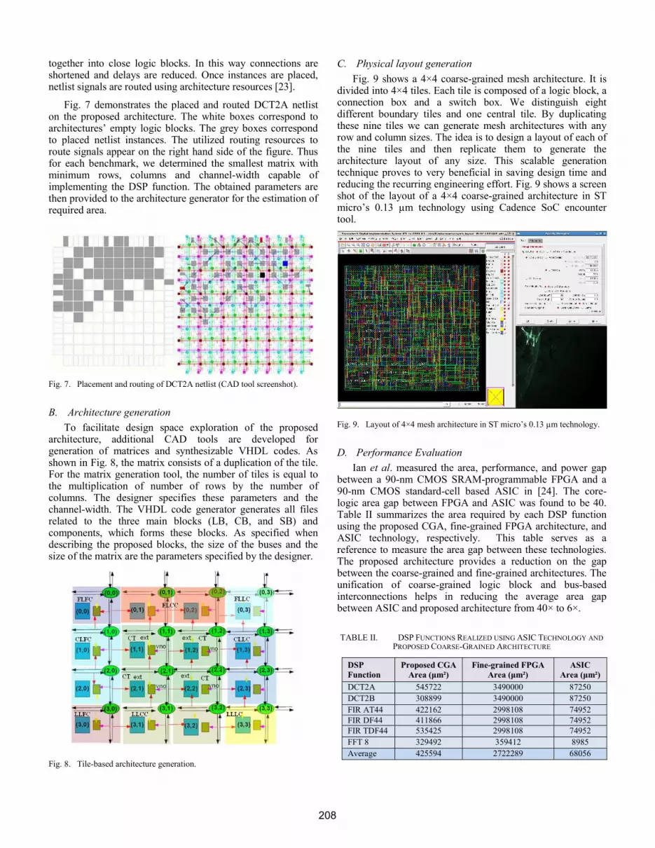
C. Physical layout generation
Fig. 9 shows a 4×4 coarse-grained mesh architecture. It is divided into 4×4 tiles. Each tile is composed of a logic block, a connection box and a switch box. We distinguish eight different boundary tiles and one central tile. By duplicating these nine tiles we can generate mesh architectures with any row and column sizes. The idea is to design a layout of each of the nine tiles and then replicate them to generate the architecture layout of any size. This scalable generation technique proves to very beneficial in saving design time and reducing the recurring engineering effort. Fig. 9 shows a screen shot of the layout of a 4×4 coarse-grained architecture in ST micro’s 0.13 µm technology using Cadence SoC encounter tool.
Fig. 9. Layout of 4×4 mesh architecture in ST micro’s 0.13 µm technology.
D. Performance Evaluation
Ian et al. measured the area, performance, and power gap between a 90-nm CMOS SRAM-programmable FPGA and a 90-nm CMOS standard-cell based ASIC in [24]. The core-logic area gap between FPGA and ASIC was found to be 40. Table II summarizes the area required by each DSP function using the proposed CGA, fine-grained FPGA architecture, and ASIC technology, respectively. This table serves as a reference to measure the area gap between these technologies. The proposed architecture provides a reduction on the gap between the coarse-grained and fine-grained architectures. The unification of coarse-grained logic block and bus-based interconnections helps in reducing the average area gap between ASIC and proposed architecture from 40× to 6×.
TABLE II. DSP FUNCTIONS REALIZED USING ASIC TECHNOLOGY AND
PROPOSED COARSE-GRAINED ARCHITECTURE
DSP
Function
Proposed CGA
Area (μm²)
Fine-grained FPGA
Area (μm²)
ASIC
Area (μm²)
DCT2A 545722 3490000 87250
DCT2B 308899 3490000 87250
FIR AT44 422162 2998108 74952
FIR DF44 411866 2998108 74952
FIR TDF44 535425 2998108 74952
FFT 8 329492 359412 8985
Average 425594 2722289 68056
208

V. CONCLUSION
In this paper, we have presented a flexible coarse-grained reconfigurable architecture for efficient realization of specific DSP applications. A pragmatic methodology to engage in such a design task is to study different DSP applications and their implemented VLSI architectures. Hence, architectural features to be supported in the target reconfigurable architecture are extracted. The proposed architecture is a matrix of identical tiles. The tile may be replicated to construct the architecture of the desired DSP function. A general architecture is introduced and the basic building blocks are described as well. Experimental results of some DSP benchmarks using the proposed technique and its comparison with other results are presented in order to demonstrate the efficiency of the proposed architecture for specific DSP applications. Comparisons between the core logic area consumed by ASIC technology and the proposed coarse-grained architecture are deduced for some DSP functions. The area gap between ASIC and the proposed architecture is found to be approximately six.
ACKNOWLEDGMENT
The authors would like to express their sincere gratitude to the Communications and Information Technologies Institute at King Abdulaziz City for Science and Technology (KACST) for supporting this research.
REFERENCES
[1] E. Chung, D. Burger, M. Butts, J. Gray, C. Thacker, K. A. Vissers, and J. Wawrzynek, “Reconfigurable computing in the era of dark silicon [panel discussion],” in Proc. 21st Annual Int. IEEE Symp. on Field-Programmable Custom Computing Machines (FCCM), April 2013.
[2] B. D. Sutter, P. Raghavan, and A. Lambrechts, “Coarse-grained reconfigurable array architectures,” in Handbook of Signal Processing Systems, 2nd ed., S. S. Bhattacharyya, E. F. Deprettere, R. Leupers, And J. Takala, Eds. New York: Springer, 2013, pp. 553-592.
[3] J. W. Yoon, J. Lee, J. Jung, S. Park, Y. Kim, Y. Paek, and D. Cho, “I2CRF: Incremental interconnect customization for embedded reconfigurable fabrics,” in Proc. Design, Automation and Test in Europe Conference and Exhibition (DATE), pp. 1346-1351, March 2011.
[4] M. Turki, Z. Marrakchi, H. Mehrez, and M. Abid, “New synthesis approach of hierarchical benchmarks for hardware pototyping,” in Proc. 8th Int. Conf. on Design and Tech. of Integrated Systems in Nanoscale Era (DTIS), pp. 16-19, March 2013.
[5] R. Hartenstein, M. Herz, T. Hoffmann, and U. Nageldinger, “KressArray Xplorer: A new CAD environment to optimize reconfigurable datapath array architectures,” in Proc. 5th Asia and South Pacific Design Automation Conf. (ASP-DAC), pp.163-168, Jan. 2000.
[6] M. Herz, “High performance memory communication architectures for coarse grained reconfigurable computing systems,” Ph.D. Dissertation, University of Kaiserslautern, Germany, 2001.
[7] T. Miyamori and K. Olukotun, “REMARC: Reconfigurable multimedia array coprocessor,” in Proc. ACM/SIGDA Int. Symp. on Field Programmable Gate Arrays (FPGA), pp. 261, Feb. 1998.
[8] A. M. Obeid, “Architectural synthesis of a coarse-grained run-time-reconfigurable accelerator for DSP applications,” Ph.D. Dissertation, University of Darmstadt, Germany, Feb. 2006.
[9] E. Mirsky and A. DeHon, “MATRIX: A reconfigurable computing architecture with configurable instruction distribution and deployable resources,” in Proc. 4th Annual IEEE Symp. on FPGAs for Custom Computing Machines (FCCM), pp. 157-166, April 1996.
[10] R. Maestre, F. J. Kurdahi, M. Fernandez, R. Hermida, N. Bagherzadeh, and H. Singh, “A framework for reconfigurable computing: task scheduling and context management,” IEEE Trans. VLSI Syst., Vol. 9, No. 6, Dec. 2001, pp. 858-873.
[11] M. B. Taylor, J. Kim, J. Miller, D. Wentzlaff, F. Ghodrat, B. Greenwald, H. Hoffman, P. Johnson, J. -W. Lee, W. Lee, A. Ma, A. Saraf, M. Seneski, N. Shnidman, V. Strumpen, M. Frank, S. Amarasinghe, and A. Agarwal, “The Raw microprocessor: A computational fabric for software circuits and general-purpose programs,” IEEE Micro, Vol. 22, No. 2, March-April 2002, pp. 25-35.
[12] E. Waingold, M. Taylor, D. Srikrishna, V. Sarkar, W. Lee, V. Lee, J. Kim, M. Frank, P. Finch, R. Barua, J. Babb, S. Amarasinghe, and A. Agarwal, “Baring it all to software: RAW machines,” IEEE Computer, Vol. 30, No. 9, Sept. 1997, pp. 86-93.
[13] J. Becker, R. Hartenstein, M. Herz, and U. Nageldinger, “Parallelization in co-compilation for configurable accelerators: A host/accelerator partitioning compilation method,” in Proc. Asia and South Pacific Design Automation Conf. (ASP-DAC), pp. 23-33, Feb. 1998.
[14] X. Wang, H. K. Nguyen, P. Cao, Z. Ki, and H. Liu, “Mapping method of coarse-grained dynamically reconfigurable computing system-on-chip of REMUS-II,” in Proc. 10th Workshop on Optimizations for DSP and Embedded Systems (ODES), pp. 45, Feb. 2013.
[15] G. Ansaloni, P. Bonzini, and L. Pozzi, “EGRA: A coarse grained reconfigurable architectural template,” IEEE Trans. VLSI Syst., Vol. 19, No. 6, June 2011, pp. 1062-1074.
[16] V. Betz and J. Rose, “VPR: A new packing, placement and routing tool for FPGA research,” in Proc. 7th Int. Workshop on Field-Programmable Logic and Applications (FPL), pp. 213-222, Sept. 1997.
[17] J. Luu, I. Kuon, P. Jamieson, T. Campbell, A. Ye, W. M. Fang, and J. Rose “VPR 5.0: FPGA CAD and architecture exploration tools with single-driver routing, heterogeneity and process scaling,” in Proc. ACM/SIGDA 17th Int. Symp. on Field Programmable Gate Arrays (FPGA), pp. 133-142, Feb. 2009.
[18] Y. Kim and R. N. Mahapatra, “Dynamic context compression for low-power coarse-grained reconfigurable architecture,” IEEE Trans. VLSI Syst., Vol. 18, No. 1, Jan. 2010, pp. 15-28.
[19] B. V. Essen, R. Panda, A. Wood, C. Ebeling, and S. Hauck, “Energy-efficient specialization of functional units in a coarse-grained reconfigurable array,” in Proc. 19th ACM/SIGDA Int. Symp. on Field-Programmable Gate Arrays (FPGAs), pp. 107-110, Feb. 2011.
[20] L. Liu, “An energy-efficient coarse-grained dynamically reconfigurable fabric for multiple-standard video decoding applications,” in Proc. Custom Integrated Cir. Conf. (CICC), pp. 1-4, Sept. 2013.
[21] M. J. Myjak and J. G. D.-Frias, “A medium-grain reconfigurable architecture for DSP: VLSI design, benchmark mapping, and performance,” IEEE Trans. VLSI Syst., Vol. 16, No. 1, Jan. 2008, pp. 14-23.
[22] H. Ghariani, “Design of a coarse grained FPGA architecture,” M.S. Thesis, National Engineering School of Sfax, University of Sfax, Tunisia, 2011.
[23] L. McMurchie and C. Ebeling, “Pathfinder: A negotiation-based performance-driven router for FPGAs,” in Proc. 3rd Int. ACM Symp. on Field-Programmable Gate Arrays (FPGA), pp. 111-117, Feb. 1995.
[24] I. Kuon and J. Rose, “Measuring the gap between FPGAs and ASICs,” in Proc. ACM/SIGDA 14th Int. Symp. on Field Programmable Gate Arrays (FPGA), pp. 21-30, Feb. 2006.
209


