Embed Size (px)
Citation preview
i
RECONFIGURABLE ULTRA WIDEBAND
ANTENNA DESIGN AND DEVELOPMENT FOR
WIRELESS COMMUNICATION
(REKAAN DAN PEMBANGUNAN ANTENA JALUR
LEBAR ULTRA BOLEH UBAH UNTUK
KOMUNIKASI WAYARLES)
THAREK ABDUL RAHMAN
RESEARCH PROJECT VOT NO.:
79028
Wireless Communication Centre
Faculty of Electrical Engineering
Universiti Teknologi Malaysia
2008

ii
ACKNOWLEDGEMENTS
Alhamdulillah. I praise and glorify be only to Allah SWT the Almighty, the Most
Beneficent and the Most Merciful, whose blessings and guidance have helped me to
be able to finish this project. I wish to thank the Ministry of Higher Education
Malaysia and Research Management Centre, Universiti Teknologi Malaysia for their
financial support during the full term of this research.
Many thanks to my colleague Dr. Razali Ngah, my Ph.D student Ms. Yusnita Rahayu
and also to my research assistant Mr. Khomeini Abu for their support. This project
will not be completed without their full encouragement and support as a solid team.
This project is a Ph.D research work that has been done intensively by Ms. Yusnita
through out her study.
Last but not least, I am grateful for the encouragement and support provided by the
many friends in Wireless Communication Centre (WCC) UTM.
iii
ABSTRACT
A few years after the early investigation on ultra wideband (UWB) wireless
system, considerable research efforts have been put into the design of UWB antennas
and systems for communications. These UWB antennas are essential for providing
wireless wideband communications based on the use of very narrow pulses on the
order of nanoseconds, covering a very wide bandwidth in the frequency domain, and
over very short distances at very low power densities. In this project, new models of
T, L and U slotted UWB antennas are proposed by studying their current distribution
characteristics. The wideband behavior is due to the fact that the currents along the
edges of the slots introduce an additional resonance, which, in conjunction with the
resonance of the main patch, produce an overall broadband frequency response
characteristic. These antennas are considerable small than others listed in the
references, which their sizes are less than a wavelength, compact, and suitable for
many UWB applications. The configuration of slots type for both patches and
feeding strip are considered as a novelty and contribution in this project. The
geometry of the antenna implies the current courses and makes it possible to identify
active and neutral zones in the antenna, thus it will be possible to fix which elements
will act on each characteristic. This project also investigated the ability of slotted
UWB antennas to reject the interference from licensed Fix Wireless Access (FWA),
High performance local area network (HIPERLAN) and wireless local area network
(WLAN) within the same propagation environment. Inserting a half-wavelength slot
structure with additional small patches gap attached have resulted frequency notched
band characteristics. The small patches gap instead of switching. The measured
return loss, radiation patterns, and phase agree well with the simulated results. The
antenna provides an omnidirectional pattern with the return loss less than -10 dB and
linear in phase.
Key researchers:
Prof. Dr. Tharek Abdul Rahman (Project Leader)
Dr Razali Ngah Ms. Yusnita Rahayu Mr. Khomeini Abu
E-mail : [email protected] Tel. No. : 07-5536106 Vote No. : 79028
iv
ABSTRAK
Beberapa tahun setelah peneraju asal pada sistem wayarles jalur sangat lebar
(UWB), sokongan penyelidikan telah ditumpukan pada reka bentuk antena UWB dan
sistem komunikasi. Antena UWB ini sangat diperlukan dalam penyediaan
komunikasi jalur lebar berasaskan penggunaan denyut yang sangat sempit dalam
kiraan nano saat, meliputi jalur yang sangat lebar dalam domain frekuensi, dan
mencakupi jarak yang sangat pendek pada kerapatan tenaga yang sangat rendah.
Dalam projek ini, model terbaru antena UWB terselot-T, L dan U di cadangkan
dengan mengkaji karakteristik pengagihan arus. Perilaku jalur lebar disebabkan pada
kenyataan bahawa arus disepanjang tepian selot memperkenalkan satu resonan
tambahan, yang mana ianya berkaitan dengan resonan tampal asas, sehingga
menghasilkan keseluruhan karakteristik sambutan frekuensi yang sangat lebar.
Antena-antena ini berukuran lebih kecil bila diperbandingkan dengan antena lainnya
yang tersenarai dalam rujukan, ukurannya lebih kecil daripada satu panjang
gelombang, padat, dan sangat sesuai digunakan untuk pelbagai aplikasi UWB.
Konfigurasi jenis selot pada kedua tampal dan jalur suapan adalah novelty dan
sebagai kontribusi dalam projek ini. Geometri antena mempengaruhi arah arus dan
dengan menentukan zon aktif dan neutral pada antenna, maka elemen yang sesuai
dapat ditentukan bagi setiap karakteristik. Projek ini juga menkaji kemampuan
antena UWB terselot untuk menolak gangguan isyarat daripada Capaian Wayarles
Tetap (FWA), Rangkaian Kawasan Tempatan Berprestasi Tinggi (HIPERLAN) dan
Rangkaian kawasan Tempatan Wayarles (WLAN) yang wujud dalam kawasan yang
sama. Kemasukan sebuah struktur selot separuh panjang gelombang dengan
penambahan sela tampal yang kecil berjaya menghasilkan karakteristik frekuensi
notched band. Sela tampal yang kecil ini digunakan bagi mewakili suatu suis.
Keputusan pengujian seperti kehilangan kembali, corak sinaran dan fasa didapati
menepati keputusan simulasi. Antena ini memberikan corak sinaran semua arah
dengan kehilangan kembali kurang daripada -10 dB dan mempunyai sambutan fasa
yang linar.
Penyelidik Utama:
Prof. Dr. Tharek Abdul Rahma (Ketua Projek)
Dr. Razali Ngah
Ms. Yusnita Rahayu
Mr. Khomeini
E-mail : [email protected] Tel. No. : 07-5536106 Vote No. : 79028
v
TABLE OF CONTENTS
CHAPTER TITLE PAGE
ACKNOWLEDGEMENTS ii
ABSTRACT iii
ABSTRAK iv
TABLE OF CONTENTS v
LIST OF TABLES viii
LIST OF FIGURES ix
LIST OF ABREVIATIONS xiv
LIST OF SYMBOLS xv
LIST OF APPENDICES xvi
1 INTRODUCTION 1
1.1 Introduction 1
1.2 Research Background 3
1.3 Problem Statements 6
1.4 Research Objective 8
1.5 Research Scope and Methodology 8
1.6 Thesis Outline 9
2 ULTRA WIDEBAND APPLICATIONS
TECHNOLOGY
11
2.1 Introduction 11
2.2 UWB Definition 13
2.2.1 Regulations Worldwide 17
2.3 A Brief History of UWB Antenna 19
2.4 Application of UWB Technology 24
2.4.1 Communication Systems 24
2.4.2 Radar Systems 26
2.4.3 Positioning Systems 26
2.4.4 UWB Over Wires 27
2.5 Short Pulse Generation 28
2.6 UWB Link Performance 29
2.7 Summary 31
3
ULTRA WIDEBAND ANTENNA DESIGN
METHODOLOGY
32
3.1 Introduction 32

vi
3.2 Fundamental Antenna Parameter 33
3.2.1 Radiation Pattern 34
3.2.2 Field Region 36
3.2.3 Directivity, Efficiency and Gain 38
3.2.4 Impedance Bandwidth 39
3.2.5 Polarization 40
3.2.6 Dispersion and Non Dispersion 41
3.3 UWB Antenna Design Methodology 42
3.3.1 Various Geometries and Perturbations 43
3.3.2 Genetic Algorithm (GA) 45
3.3.3 Resonance Overlapping 47
3.4 Reconfigurable UWB Antenna 48
3.4.1 Reconfigurability Antenna Parameters 48
3.4.1.1 Frequency Response
Reconfigurability 48
3.4.1.2 Polarization Reconfigurability 49
3.4.1.3 Radiation Pattern
Reconfigurability 49
3.4.2 Design Methodology 50
3.5 Theory Characteristic Modes for Planar
Monopole Antennas 52
3.6 Summary 53
4 SLOTTED AND RECONFIGURABLE UWB
ANTENNA DESIGN
55
4.1 Introduction 55
4.2 Slotted UWB Antenna Design Consideration 56
4.2.1 Various Bevels and Notches 56
4.2.2 Current Distribution Behavior 71
4.2.3 Various Slots 80
4.2.4 Feed Gap and Slotted Ground Plane 88
4.2.5 Substrate Permittivity and Thickness 89
4.3 Reconfigurable Slotted UWB Antenna Design
Consideration 101
4.3.1 Reconfigurable Modified T Slotted
Antenna 102
4.3.2 Reconfigurable Modified L and U
Slotted Antenna 107
4.4 Summary 110
5 RESULTS AND DISCUSSIONS 111
5.1 Introduction 111
5.2 Final Design of Slotted UWB Antenna Design
and Experimental Verification
111
5.2.1 Simulated and Measured Return Loss 113
5.2.2 Simulated and Measured VSWR 116
vii
5.2.3 Simulated and Measured Gain 117
5.2.4 Various Slot Design 125
5.2.4.1 Various T Slot Design 125
5.2.4.2 Various L and U Slot Design 129
5.3 Final Design of Reconfigurable Slotted UWB 134
5.4 Spherical Near Field Testing 140
5.4.1 Radiation Pattern of T Slotted Antenna
with Slotted Ground Plane
142
5.4.2 Radiation Pattern of L and U Slotted
Antenna
148
5.4.3 Radiation Pattern of Reconfigurable T
Slotted UWB Antenna
153
5.4.4 Radiation Pattern of Reconfigurable L
and U Slotted Antenna
158
5.5 Estimating Error Analysis in Radiation Pattern
Measurement
164
5.6 Key Contributions 168
5.7 Summary 169
6 CONCLUSIONS AND FUTURE WORKS 170
6.1 Conclusion 170
6.2 Future Works 172
REFERENCES
References 174-186
APPENDICES
Appendix A 187
viii
LIST OF TABLES
TABLE NO. TITLE PAGE
2.1 FCC limits for indoor and handheld systems 15
2.2 UWB limits for the Singapore UFZ 19
4.1 The effect of notches to the simulated -10dB bandwidths of
the proposed antenna
60
4.2 The effect of bevels to the simulated -10dB bandwidths of
the proposed antenna
62
4.3 The effect of bevels coupling notches to the simulated -
10dB bandwidths of the proposed antenna
66
4.4 Trapezoidal and pentagonal fractional bandwidth with
respect to the simulated return loss of -10dB
68
4.5 The effect of smooth bevels and upper edge transition to
the simulated -10dB bandwidths of the proposed antenna
70
4.6 Slot size of the slotted rectangular antenna in Figure 4.15 82
4.7 Slot size of the slotted pentagonal antenna in Figure 4.16 83
4.8 Simulated -10dB bandwidths of the T slotted antenna for
different feed gaps of the ground plane
89
4.9 Simulated -10dB bandwidths of the L and U slotted antenna
for different feed gaps of the ground plane
92
5.1 The simulated maximum gain and directivity of T slotted
antenna with slotted ground plane
118
5.2 The simulated radiation properties of T slotted antenna with
slotted ground plane
123
5.3 The simulated maximum gain and directivity of L and U
slotted antenna
124
5.4 The simulated radiation properties of L and U slotted
antenna
125
5.5 Near field error analysis for spherical measurement 165
ix
LIST OF FIGURES
FIGURE NO. TITLE PAGE
2.1 UWB spectral power density mask (FCC and ETSI) 14
2.2 Ultra wideband communications spread transmitting energy
across a wide spectrum of frequency
16
2.3 Proposed spectral mask of ECC 17
2.4 Proposed spectral mask in Asia 18
3.1 Dipole model for simulation and simulated 3D radiation
pattern 35
3.2 Representation plots of the normalized radiation pattern of
a microwave antenna in (a) polar form and (b) rectangular
form.
36
3.3 Field regions of antenna 37
3.4 Some wave polarization states where the wave is approaching 41
4.1 Various type of polygonal monopole antennas (a) various
steps notches at the bottom and (b) various bevel at the
bottom
57
4.2 (a) Simulated return loss curves and (b) input impedance
for various notches
59
4.3 (a) Simulated return loss curves (b) input impedance for
various bevels
61
4.4 Various type polygonal monopole antennas (a) combination
of notch and bevel, (b) trapezoidal and pentagonal bevels
and (c)smooth bevels at the bottom
63
4.5 (a) Simulated return loss curves (b) input impedance for
various pair bevel and notches
65
4.6 (a) Simulated return loss curves (b) input impedance for
trapezoidal and various pentagonal
67
4.7 (a) Simulated return loss curves (b) input impedance for
various transitions with smooth bevel
69
4.8 Simulated comparison return loss curves for each best type
of antenna
70
4.9 Simulated current distribution for three model antennas
with affect to the impedance bandwidth (a) rectangular (b)
rectangular with two notches (c) pentagonal
72
4.10 Simulated return loss for three model antennas with affect
to the impedance bandwidth
74
4.11 Neutral zones for various frequencies of pentagonal
antenna (a) 5 GHz (b) 8GHz (c) 10.5 GHz
75
4.12 (a) The simulated radiation pattern for various diamond
slots of pentagonal antenna at 5.25 GHz (b) the simulated
return loss for various diamond slots
77
4.13 Neutral zones for various frequencies of rectangular with
two notches antenna (a) 4.5 GHz (b) 5 GHz (c) 8 GHz
78
x
4.14 (a) The simulated radiation pattern for various rectangular
slots of rectangular antenna with two notches at 5.25 GHz
(b) The simulated return loss for various rectangular slots
79
4.15 Various slots design of rectangular with two notches
antennas
81
4.16 Various slots design of pentagonal antennas 81
4.17 The simulated return loss of various slot designs for
pentagonal antennas
84
4.18 The simulated return loss of various slot designs for
rectangular with two notches antennas
85
4.19 The simulated radiation pattern of various slot designs (a)
rectangular with two notches (b) pentagonal
87
4.20 Simulated return loss curves of T slotted antenna for
different feed gaps
89
4.21 Simulated input impedance curves of T slotted antenna for
different feed gaps (a) real part and (b) imaginary part
91
4.22 Simulated return loss curves of L and U slotted antenna for
different feed gaps
92
4.23 Simulated input impedance curves of L and U slotted
antenna for different feed gaps (a) real part (b) imaginary
part
93
4.24 Geometry of staircase slotted ground plane 94
4.25 The effect of various length slotted ground plane to the
antenna performance (a) T slotted antenna (b) L and U
slotted antenna
95
4.26 The effect of various width slotted ground plane to the
antenna performance (a) T slotted antenna (b) L and U
slotted antenna
96
4.27 The effect of various number slotted ground plane to the
antenna performance (a) T slotted antenna (b) L and U
slotted antenna
98
4.28 Simulated return loss curves of T slotted antenna for
different substrate permittivity
99
4.29 Simulated return loss curves of L and U slotted antenna for
different substrate permittivity and thickness
100
4.30 The simulated return loss of T slotted antenna with
different length of patch radiator
101
4.31 The reconfigurable modified T slotted antenna 103
4.32 Switching configuration for T slotted antenna: (a) notched
at FWA, (b) UWB bandwidth (w/o notched), (c) notched at
HIPERLAN, and (d) notched at WLAN
105
4.33 The simulated VSWR for reconfigurable modified T slotted
antenna
106
4.34 Switching configuration for L and U slotted antenna: (a)
UWB bandwidth (w/o notched), (b) notched at FWA, (c)
notched at HIPERLAN, and (d) notched at WLAN
108
4.35 The simulated VSWR for reconfigurable modified L and U
slotted antenna
109
5.1 The geometry and prototypes of final design for slotted
UWB antennas: (a) geometry, (b) prototypes
112
xi
5.2 The measured and simulated return loss for T slotted
antenna: (a) with slotted ground plane and (b) without
slotted ground plane
114
5.3 The measured and simulated return loss for L and U slotted
antenna
115
5.4 The measured and simulated VSWR for both antennas 117
5.5 The simulated maximum gain and directivity of T slotted
antenna with slotted ground plane
118
5.6 The measured relative gain for T slotted antenna with
slotted ground plane with respect to the peak plot in the H-
plane: (a) 4 GHz, (b) 5.8 GHz, and (c) 10.6 GHz
119
5.7 The measured relative gain for L and U slotted antenna
with respect to the peak plot in the H-plane: (a) 4 GHz, (b)
5.8 GHz, and (c) 10.6 GHz
121
5.8 The simulated antenna and radiation efficiency of T slotted
antenna with slotted ground plane
122
5.9 The simulated maximum gain and directivity of L and U
slotted antenna
123
5.10 The simulated antenna and radiation efficiency of L and U
slotted antenna
124
5.11 The simulated current distribution for T slotted with slotted
ground plane antenna: (a) 3 GHz, (b) 5.5 GHz, and (c) 9
GHz
126
5.12 The simulated return loss of various T slots design for T
slotted with slotted ground plane antenna
127
5.13 The simulated return loss of various width of T slots design 127
5.14 The simulated current distribution on the antenna by
varying its height of T slot on the patch radiator for
different frequency: (a) both length 3 mm, (b) both length 5
mm, and (c) length 4 and 3mm
128
5.15 The simulated return loss of various heights for upper T
slot
129
5.16 The simulated current distribution of 3, 6, and 9 GHz for L
and U slotted antenna
130
5.17 The simulated return loss of various L and U slots design
for L and U slotted antenna
131
5.18 The simulated return loss of various width of L and U slots
design
132
5.19 The simulated current distribution on the antenna by
varying its length of L and U slot on the patch radiator for
different frequency: (a) vary L, (b) vary U, and (c) vary
both L and U
133
5.20 The simulated return loss of L and U slotted antenna with
different length slot
134
5.21 Three prototypes of T slotted antennas with notched band at
FWA (left), notched at HIPERLAN (middle) and notched
at WLAN (right): (a) geometry of reconfigurable T slotted
antenna and (b) photograph of prototype
135
5.22 The measured VSWR for the three prototypes of modified
T slotted antenna
136
xii
5.23 The measured phase for modified T slotted antenna 137
5.24 Three prototypes of modified L and U slotted antenna for
band notched at FWA (top), at HIPERLAN (left) and at
WLAN (right): (a) geometry and (b) photograph
138
5.25 The measured VSWR for L and U slotted antenna 139
5.26 The measured phase of L and U slotted antenna with
HIPERLAN notched band
140
5.27 The radiation pattern measurement setup inside the
anechoic chamber room
141
5.28 Coordinate system for typical spherical near-field rotator
system
142
5.29 The measured and simulated E and H planes at 4 GHz: (a)
measured and simulated E-planes and (b) measured and
simulated H-planes
144
5.30 The measured and simulated E and H planes at 5.8 GHz:
(a) measured and simulated E-planes and (b) measured and
simulated H-planes
145
5.31 The measured and simulated E and H planes at 10.6 GHz:
(a) measured and simulated E-planes and (b) measured and
simulated H-planes
146
5.32 The measured 3D radiation pattern: (a) 4 GHz and (b) 5.8
GHz
147
5.33 The measured 3D radiation pattern at 10.6 GHz: (a) side
view and (b) top view
148
5.34 The measured and simulated E and H planes at 4 GHz: (a)
measured and simulated E-planes and (b) measured and
simulated H-planes
149
5.35 The measured and simulated E and H planes at 5.8 GHz:
(a) measured and simulated E-plane and (b) measured and
simulated H-planes
150
5.36 The measured and simulated E and H planes at 10.6 GHz:
(a) measured and simulated E-planes and (b) measured and
simulated H-planes
151
5.37 The measured 3D radiation pattern: (a) 4 GHz (b) 5.8 GHz 152
5.38 The measured 3D radiation pattern at 10.6 GHz 153
5.39 The measured and simulated E and H-planes for T slotted
antenna notched at FWA: (a) 4 GHz and (b) 5.8 GHz
154
5.40 The measured and simulated E and H planes for T slotted
antenna notched at HIPERLAN: (a) 4 GHz and (b) 5.8 GHz
155
5.41 The measured and simulated E and H planes for T slotted
antenna notched at WLAN: (a) 4 GHz and (b) 5.8 GHz
156
5.42 The measured 3D radiation patterns for T slotted notched
band antenna: (a) band notched at FWA and (b) band
notched at HIPERLAN
157
5.43 The measured 3D radiation patterns for T slotted notched
band at WLAN
158
5.44 The measured and simulated E and H planes for L and U
slotted notched antenna at FWA (a) 4 GHz and (b) 5.8 GHz
159
xiii
5.45 The measured and simulated E and H planes for L and U
slotted antenna notched at HIPERLAN: (a) 4GHz and (b)
5.8 GHz
160
5.46 The measured and simulated E and H planes for L and U
slotted antenna notched at WLAN: (a) 4 GHz and (b) 5.8
GHz
161
5.47 The measured 3D radiation patterns for L and U slotted
antenna notched band at FWA: (a) 4 GHz and (b) 5.8 GHz
162
5.48 The measured 3D radiation patterns for L and U slotted
antenna notched band at HIPERLAN: (a) 4 GHz and (b) 5.8
GHz
163
5.49 The measured 3D radiation patterns for L and U slotted
antenna notched band at WLAN: (a) 4 GHz and (b) 5.8
GHz
164
5.50 An Example of results of random errors for L and U slotted
antenna at 5.8 GHz
166
xiv
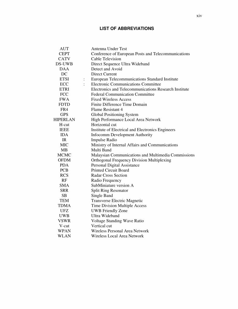
LIST OF ABBREVIATIONS
AUT Antenna Under Test
CEPT Conference of European Posts and Telecommunications
CATV Cable Television
DS-UWB Direct Sequence Ultra Wideband
DAA Detect and Avoid
DC Direct Current
ETSI : European Telecommunications Standard Institute
ECC : Electronic Communications Committee
ETRI Electronics and Telecommunications Research Institute
FCC Federal Communication Committee
FWA Fixed Wireless Access
FDTD Finite Difference Time Domain
FR4 Flame Resistant 4
GPS Global Positioning System
HIPERLAN High Performance Local Area Network
H-cut Horizontal cut
IEEE Institute of Electrical and Electronics Engineers
IDA Infocomm Development Authority
IR Impulse Radio
MIC Ministry of Internal Affairs and Communications
MB Multi Band
MCMC Malaysian Communications and Multimedia Commissions
OFDM Orthogonal Frequency Division Multiplexing
PDA Personal Digital Assistance
PCB Printed Circuit Board
RCS Radar Cross Section
RF Radio Frequency
SMA SubMiniature version A
SRR Split Ring Resonator
SB Single Band
TEM Transverse Electric Magnetic
TDMA Time Division Multiple Access
UFZ UWB Friendly Zone
UWB Ultra Wideband
VSWR Voltage Standing Wave Ratio
V-cut Vertical cut
WPAN Wireless Personal Area Network
WLAN Wireless Local Area Network
xv
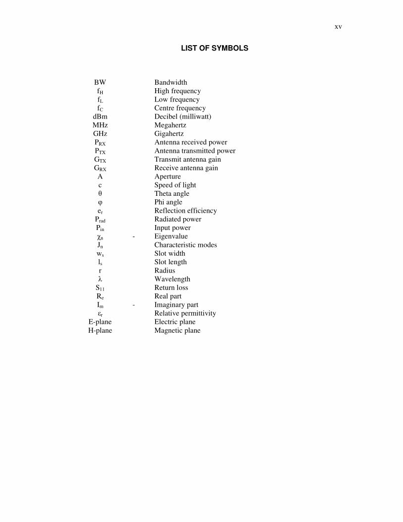
LIST OF SYMBOLS
BW Bandwidth
fH High frequency
fL Low frequency
fC Centre frequency
dBm Decibel (milliwatt)
MHz Megahertz
GHz Gigahertz
PRX Antenna received power
PTX Antenna transmitted power
GTX Transmit antenna gain
GRX Receive antenna gain
A Aperture
c Speed of light
θ Theta angle
φ Phi angle
er Reflection efficiency
Prad Radiated power
Pin Input power
χn - Eigenvalue
Jn Characteristic modes
ws Slot width
ls Slot length
r Radius
λ Wavelength
S11 Return loss
Re Real part
Im - Imaginary part
εr Relative permittivity
E-plane Electric plane
H-plane Magnetic plane
xvi
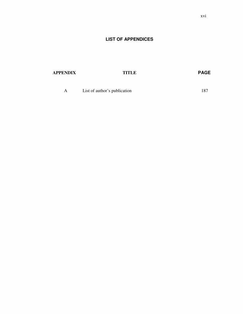
LIST OF APPENDICES
APPENDIX TITLE PAGE
A List of author’s publication 187
1
CHAPTER 1
INTRODUCTION
1.1 Introduction
Ultra Wideband (UWB) is currently receiving special attention and is quite a
hot topic in industry and academia. UWB short-range wireless communication is
different from a traditional carrier wave system. UWB waveforms are short time
duration and have some rather unique properties. The benefits of UWB technology
are derived from its unique characteristics that are the reasons why it presents a more
eloquent solution to wireless broadband than other technologies. The unique
characteristics are listed below [1]:
Firstly, an inherent capability for integration in low cost, low power
Integrated Circuit (IC) processes. UWB system based on impulse radio features low
cost and low complexities which arise from the essentially base-band nature of the
signal transmission. UWB does not modulate and demodulate a complex carrier
waveform, so it does not require components such as mixers, filters, amplifiers and
local oscillators.
Secondly, UWB has an ultra wide frequency bandwidth; it can achieve huge
capacity as high as hundreds of Mbps or even several Gbps with distances of 1 to 10
meters [2]. Thus, the UWB is a promising technology for Wireless Personal Area
Network (WPAN). In recent years, more interests have been put into WPAN
technology worldwide. The future WPAN aims to provide reliable wireless
connections between computers, portable devices and consumer electronics within a
2
short range. Furthermore, fast data storage and exchange between these devices will
also be accomplished. This requires a data rate which is much higher than what can
be achieved through currently existing wireless technologies.
Thirdly, UWB system is extremely fine time and range solution even through
lossy, opaque media. And fourthly, UWB system has immunity from multipaths.
Fifthly, non-interfering operation with existing services. In spreading signals
over very wide bandwidths, the UWB concept is especially attractive since it
facilitates optimal sharing of a given bandwidth between different systems and
applications. UWB systems are highly frequency adaptive, enabling them to be
positioned anywhere within the RF spectrum. This feature avoids interference to
existing services, while fully utilizing the available spectrum. UWB systems operate
at extremely low power transmission levels. Therefore, UWB short-range radio
technology complements other longer-range radio technologies such as Wireless
Fidelity (WiFi), Worldwide Interoperability for Microwave Access (WiMAX), and
cellular wide area communications.
Lastly, UWB has low probability of detection and interception. UWB
provides high secure and high reliable communication solutions. Due to the low
energy density, the UWB signal is noise-like, which makes unintended detection
quite difficult. Furthermore, the “noise-like" signal has a particular shape; in contrast,
real noise has no shape. For this reason, it is almost impossible for real noise to
obliterate the pulse because interference would have to spread uniformly across the
entire spectrum to obscure the pulse. Interference in only part of the spectrum
reduces the amount of received signal, but the pulse still can be recovered to restore
the signal. Hence UWB is perhaps the most secure means of wireless transmission
ever previously available [3].
As with any technology, there are always applications that may be better
served by other approaches. For example, for extremely high data rate (10’s of
Gigabits/second and higher), point-to-point or point-to-multipoint applications, it is
difficult today for UWB systems to compete with high capacity optical fiber or
optical wireless communications systems. The high cost associated with optical fiber
3
installation and the inability of an optical wireless signal to penetrate a wall
dramatically limits the applicability of optically-based systems for in-home or in-
building applications. In addition, optical wireless systems have extremely precise
pointing requirements, obviating their use in mobile environments.
1.2 Research Background
The UWB technology has experienced many significant developments in
recent years. However, there are still challengers in making this technology live up to
its full potential. One particular challenge is the UWB antenna design. UWB
technology has had a substantial effect on antenna design. The UWB antennas have
to be able to transmit pulses as accurately and efficiently as possible. The spectrum
allocated certainly requires transmitters and receivers with wideband antennas.
Thorough literature survey, there are two vital design considerations in UWB
radio systems. One is radiated power density spectrum shaping must comply with
certain emission limit mask for coexistence with other electronic systems [4].
Another is that the design source pulses and transmitting/receiving antennas should
be optimal for performance of overall systems [5]. Emission limits will be crucial
considerations for the design of source pulses and antennas in UWB systems.
The main challenge in UWB antenna design is achieving the extremely wide
impedance bandwidth while still maintaining high radiation efficiency. By definition,
an UWB antenna must be operable over the entire 3.1 GHz - 10.6 GHz frequency
range. Therefore, the UWB antenna must achieve almost a decade of impedance
bandwidth, spanning 7.5 GHz. The high radiation efficiency is also required
especially for UWB applications to ensure the transmit power spectral density
requirement achieved. Conductor and dielectric losses should be minimized in order
to maximize radiation efficiency. High radiation efficiency is imperative for an
UWB antenna because the transmit power spectral density is excessively low.
Therefore, any excessive losses incurred by the antenna could potentially
compromise the functionality of the system.
4
Next, the performance of UWB antenna is required to have a constant group
delay. Group delay is given by the derivative of the unwrapped phase of an antenna.
If the phase is linear throughout the frequency range, the group delay will be constant
for the frequency range. This is an important characteristic because it helps to
indicate how well a UWB pulse will be transmitted and to what degree it may be
distorted or dispersed. The antennas required to have a non-dispersive characteristic
in time and frequency, providing a narrow, pulse duration to enhance a high data
throughput. It is also a parameter that is not typically considered for narrowband
antenna design because linear phase is naturally achieved for narrowband resonance.
In addition, a nearly omni-directional radiation pattern is desirable in that it
enables freedom in the receiver and transmitter location. This implies maximizing
the half power beam-width and minimizing directivity and gain. It is also highly
desirable that the antenna feature low profile and compatibility for integration with
printed circuit board (PCB) [6].
A good design of UWB antenna should be optimal for the performance of
overall system. For example, the antenna should be designed such that the overall
device (antenna and Radio Frequency (RF) front end) complies with the mandatory
power emission mask given by the Federal Communication Committee (FCC) or
other regulatory bodies [6]. But not the least important, a UWB antenna is required
to achieve good time domain characteristics. Minimum pulse distortion in the
received waveform, is a primary concern of a suitable UWB antenna because the
signal is the carrier of useful information. For the narrow band case, it is
approximated that an antenna has same performance over the entire bandwidth and
the basic parameters, such as gain and return loss, have little variation across the
operational band.
Today the state of the art of UWB antennas focuses in the microstrip, slot and
planar monopole antennas with different matching techniques to improve the
bandwidth ratio without loss of its radiation pattern properties [7]. The expected
antennas are small size, omni directional patterns, and simple structure that produce
low distortion but can provide large bandwidth [8].
5
In the past, one serious limitation of microstrip antennas was the narrow
bandwidth characteristic, being 15% to 50% that of commonly used antenna
elements such as dipoles, and slots [9]. This limitation was successfully removed
achieving a matching impedance bandwidth of up 90%. To increase the matching
impedance bandwidth ratio it was necessary to increase the size, height, volume or
feeding and matching techniques [10]. Variety of matching techniques have been
proposed in the literature reviews, such as the use of slot [11][12], bevel or taper at
the bottom of patch [13], notch and partial ground plane [12]. There is a growing
demand for small and low cost UWB antennas that can provide satisfactory
performances in both frequency domain and time domain.
The planar monopole antennas are promising antennas for UWB applications
due to their simple structure, low profile, easy to fabricate and UWB characteristics
with nearly omni-directional radiation patterns [6][14][15]. Planar monopole
antennas feature broad impedance bandwidth but somewhat suffer high cross-
polarization radiation levels. The large lateral size or asymmetric geometry of the
planar radiator causes the cross-polarized radiation. Fortunately, the purity of the
polarization issue is not critical, particularly for the antennas used for portable
devices [16]. There are several UWB planar antenna designs, including planar half-
disk antenna [17], planar horn antenna [18], and metal plate antenna [19], have been
reported.
Even though UWB is recommended by the FCC of United States (U.S) to
operate with maximum in-band effective incident radiated power of -41.3 dBm/MHz
within the band from 3.1 GHz to 10.6 GHz, there have been almost 1000 complaints
logged against UWB deployment so far [20]. Evaluation of interference between
Multiband Orthogonal Frequency Division Multiplexing (MB-OFDM) UWB and
Wireless Local Area Network (WLAN) systems using a Gigahertz Transverse
Electromagnetic (GTEM) cell has been proposed in [21]. As a result, when the
frequencies of the MB-OFDM UWB corresponded to out-of-band radiation for 11a
(Band #3), MB-OFDM UWM did not interfere with the WLAN system. In the other
hand, when frequencies of the MB-OFDM UWB corresponded to in-band radiation
for 11a (Band #4), although the interference power of MB-OFDM UWB was less
than receiver noise, the MB-OFDM UWB systems interfered with the WLAN.
6
Evaluation of interference between Direct Sequence spread spectrum UWB
(DS-UWB) and WLAN systems using a GTEM cell has already been presented a
year before in [22]. Even if the UWB signal is smaller than the receiver noise of
WLAN, the throughput characteristics deteriorate than those in case of the non-
interference [22]. Therefore, recently the consideration of UWB antennas is not only
focused on an extremely wide frequency bandwidth, but on the ability of rejecting
the interference from WLAN 11.a (5725 - 5825 MHz) and High Performance Local
Area Network (HIPERLAN) (5150 - 5350 MHz) within the same propagation
environment [23].
To avoid the interference between the UWB, WLAN and HIPERLAN
systems, a band-notch filter in UWB systems is necessary. However, the use of a
filter will increase the complexity of the UWB systems [24]. One of the solutions
proposed, as far as antennas are concerned, was to design frequency notched antenna.
Therefore, several techniques used to introduce a notched band for rejecting the
WLAN and HIPERLAN interference have been investigated, which include such as
inserting a half-wavelength slot structure [23][25]-[29], slitting on the edges [30]-
[31], utilizing fractal feeding structure [32], and parasitic quarter-wave patch [33] or
parasitic open-circuit stub [34]. With the notched band characteristic, the antenna
allows to reconfigurable its frequency that only responsive to other frequencies
beyond the rejection bands within UWB bandwidth.
1.3 Problem Statements
One of the critical issues in this UWB antenna design is the size of the
antenna for portable devices, because the size affects the gain and bandwidth greatly
[35]. Therefore, to miniaturize the antennas capable of providing ultra wide
bandwidth for impedance matching and acceptable gain will be a challenging task
[5]. Planar monopole is used to reduce the size of the proposed antennas. Some
novelty UWB planar monopole antennas are investigated in detail in order to
understand their operations; find out the mechanism that leads to UWB
7
characteristics and to obtain some quantitative guidelines for designing of this type
of antennas.
In order to obtain the ultra wide bandwidth and omni directional radiation
pattern, four matching techniques are applied to the proposed UWB antennas, such
as the use of slots, the use of bevels and notches at the bottom of patch, the
truncation ground plane, and the slotted ground plane. All these techniques are
applied to the small UWB antenna without degrading the required UWB antenna’s
performance. The size of slots, bevels and notches are critically affect to the
impedance bandwidth. The distance between truncation ground plane to the bottom
of the patch is as matching point, where it determines the resonance frequency. To
ensure the broad bandwidth can be obtained, the proper designs on those parameters
are required.
The theory characteristic modes are used to design and optimize the proposed
UWB antennas as well as some new designs are studied. From the study of the
behavior of characteristic modes, important information about the resonant frequency
and the bandwidth of an antenna can be obtained. The current behaviors of the
antenna are investigated in order to obtain several new slotted UWB antennas. High
radiation efficiency and linear phase are also required.
A licensed Fix Wireless Access (FWA) for point to multipoint radio systems
assigned by Malaysian Communications and Multimedia Commissions (MCMC) for
3.4 to 3.7 GHz is considered giving a potential interference to UWB application.
This is due to the allocation frequency for this FWA within the UWB range. Thus,
the proposed notched antenna is not only designed to reject interference from
WLAN, HIPERLAN but also from FWA. In order to meet the goal, the previous
designed UWB slotted antenna is chosen as a basic type of reconfigurable slotted
UWB antennas. This is due to the slot antennas are good candidate to meet the needs
for UWB communication and antenna size reduction due to their compact and
broadband. To design this reconfigurable UWB slotted antenna with three notched
bands characteristics by using a simple structure of antenna is very challenging task.
In this thesis, this antenna is known as reconfigurable UWB slotted antenna. The
reconfigurability characteristic means the ability of UWB slotted antenna to reject
8
certain frequencies by using some small gaps, instead of switches, without any
degrading the radiation pattern. The controllable slot length by the gaps is intended
to reject the required frequencies.
Finally, two types of UWB antennas have been designed and resulted in this
thesis. One is slotted antenna type for general UWB applications. The second one is
the reconfigurable UWB slotted antenna. This second type of antenna is used to
reject the interference from existing wireless communication systems within the
UWB range such as FWA, HIPERLAN, and WLAN bands. However this is still the
newest issue, the existing publications mostly on UWB antenna with notched bands
on HIPERLAN/WLAN bands. This thesis is working with an additional notched on
FWA band in order to give contribution in UWB antenna development.
1.4 Research Objective
The main purpose of this research is to propose small novel types of
reconfigurable UWB antennas. The proposed antennas have capability to
reconfigurable their frequency to a narrower bandwidth over UWB bandwidth (3.1
GHz - 10.6 GHz) while excepting from interference with existing FWA,
HIPERLAN, and WLAN bands with band notched characteristics.
1.5 Research Scope and Methodology
The research scope is focused on slotted UWB antennas designs which
provide an ultra wide bandwidth. Truncation ground plane and notches/bevels
techniques are added to improve the impedance matching. The reconfigurability
antennas characteristics are achieved by varying the length of slots with on/off the
small gaps, instead of switches. In order to achieve the objective, a number of
activities have been identified, as outline below:
9
• Investigate characteristics of UWB antenna by means of simulation and
numerical analysis.
• Simulate the UWB antenna design model using antenna simulation software before the actual prototype built.
• Integrate some small gaps into the proposed antenna to evaluate the reconfigurable characteristics performance.
• Develop a new design prototype of reconfigurable UWB antenna.
• Antenna performance evaluation and optimization.
1.6 Thesis Outline
The thesis is divided into six chapters. Following is an introductory chapter
that defines the importance of this research, objective, and scope. The introduction of
UWB technology, the challenges in UWB antenna design, the UWB notched band
characteristics and the current issues are also highlighted. The review of UWB
applications technology is given in Chapter 2. This chapter begins by the UWB
history and definition of UWB signal with some international standardization on it. A
wide variety of wideband antennas are presented as well. Some applications applied
for this UWB technology such as communication system, radar system and
positioning system are discussed. With UWB techniques, it becomes feasible to fuse
these unique capabilities into a single system. The review of UWB antenna with
notched band characteristics with capability to reject interference generated between
other communication systems is presented. Finally, overview of short pulse
generation and link performance are discussed.
The literature review examined a comprehensive background of other related
research works and the fundamental antenna parameters that should be considered in
designing UWB antenna, and potential technologies for physical construction given
in Chapter 3. Design methodology applied in this proposed UWB antenna and
reconfigurable UWB antenna is discussed in detail. The key differences and
considerations for UWB antenna design are also discussed in depth as several
10
antennas are presented with these considerations in mind. Several bandwidth
enhancement techniques such as various geometry perturbation and Genetic
Algorithm will be highlighted in order to obtain optimization in size and
performance.
Chapter 4 elaborates on the design methodology mentioned in the previous
sections. Some new novelty slotted UWB antennas and reconfigurable UWB
antennas are presented and design requirements, general strategy for the design are
discussed in detail. By properly design the slots and gaps have provided band
notched characteristics at 3.4 - 3.7 GHz and 5.150 - 5.850 GHz. The novelty is in
term of the type of slots used and it is considered as a contribution in this thesis.
Chapter 5 presents the results and discussion. Simulated and measured results
are compared. The experimental verification process is explained with numerical
analysis given. The key contributions in this thesis are highlighted. Finally, some
recommendations on further work as well as a concluding statement are given in
Chapter 6.
11
CHAPTER 2
ULTRA WIDEBAND APPLICATIONS TECHNOLOGY
2.1 Introduction
Although often considered a recent breakthrough in broadband wireless
technology, the concept of UWB dates back many decades. The early UWB systems,
designed for the U.S military and government agencies, included such applications as
covert (low probability of detection and intercept) radar and communication systems.
Recent advancements in chip development have made UWB more viable for
commercial and civilian use. Freescale Semiconductor was the first company to
produce UWB chips in the world and its XS110 solution is the only commercially
available UWB chipset to date [6]. It provides full wireless connectivity
implementing DS-UWB. The chipset delivers more than 110 Mbps data transfer rate
supporting applications such as streaming video, streaming audio, and high-rate data
transfer at very low levels of power consumption.
Contributions to the development of a field addressing UWB RF signals
commenced in the late 1960's on time-domain electromagnetic [37] as carrier-free,
base-band or impulse technology [38] by the pioneering contributions of Harmuth at
Catholic University of America, Ross and Robbins at Sperry Rand Corporation and
Paul van Etten at the USAF's Rome Air Development Center. The Harmuth books
and published papers, 1969 - 1984, placed in the public domain the basic design for
UWB transmitters and receivers [39]-[45]. At approximately the same time and
independently, the Ross and Robbins (R & R) patents, 1972 - 1987, pioneered the
12
use of UWB signals in a number of application areas, including communications and
radar using coding schemes [46]-[53]. Ross' US Patent 3,728,632 dated 17th April,
1973, is a landmark patent in UWB communications [42]. Van Etten's empirical
testing of UWB radar systems resulted in the development of system design and
antenna concepts. In 1974, Morey designed a UWB radar system for penetrating the
ground, which was to become a commercial success at Geophysical Survey Systems,
Inc. (GSSI) [54].
By the early 1970s the basic designs for UWB signal systems were available
and there remained no major impediment to progress in perfecting such systems.
After the 1970s, the only innovations in the UWB field could come from
improvements in particular instantiations of subsystems, but not in the system
concept itself. The basic components known were pulse train generators, pulse train
modulators, switching pulse train generators, detection receivers and wideband
antennas. Moreover, particular instantiations of the subcomponents and
methodologies known were avalanche transistor switches, light responsive switches,
use of sub-carriers in coding pulse trains, leading edge detectors, ring demodulators,
mono-stable multi-vibrator detectors, integration and averaging matched filters,
template signal match detectors, correlation detectors, signal integrators,
synchronous detectors and antennas driven by stepped amplitude input [38].
Through the late 1980’s, UWB technology was referred to as base-band,
carrier free or impulse technology, as the term ultra wideband was not used until
1989 by the U.S. Department of Defense. Until the recent FCC allocation of the
UWB spectrum for unlicensed use, all UWB applications were permissible only
under a special license. The interest seems to be growing exponentially now,
precipitated by the FCC allocation in 2002 of the UWB spectrum, with several
researchers exploring RF design, circuit design, system design and antenna design,
all related to UWB applications.
13
2.2 UWB Definition
On February 14, 2002, a UWB frequency allocation has been made by the
U.S FCC in the range from 1.99 GHz - 10.6 GHz, 3.1 GHz - 10.6 GHz, or below 960
MHz depending on the particular application [4] and work is underway by regulatory
bodies to achieve the same in Europe and Asia [55]. Since then, UWB technology
has been regarded as one of the most promising wireless technologies that promises
to revolutionize high data rate transmission and enables the personal area networking
industry leading to new innovations and greater quality of services to the end users.
The FCC has defined an UWB device as any device with a -10 dB fractional
bandwidth, greater than 20% or occupying at least 500 MHz of the spectrum [4].
Most narrowband systems occupy less than 10% of the center frequency bandwidth,
and are transmitted at far greater power levels. For example, if a radio system were
to use the entire UWB spectrum from 3.1-10.6 GHz, and center about almost any
frequency within that band, the bandwidth used would have to be greater than 100%
of the center frequency in order to span the entire UWB frequency range. By
contrast, the 802.11b radio system centers about 2.4 GHz with an operating
bandwidth of 80 MHz. This communication system occupies a bandwidth of only
1% of the center frequency.
The FCC also regulated the spectral shape and maximum power spectral
density (-41.3 dBm/MHz) of the UWB radiation in order to limit the interference
with other communication systems. The power spectral density is the average power
in the signal per unit bandwidth and hence provides important information on the
distribution of power over the RF spectrum. The European Telecommunications
Standard Institute (ETSI) regulations in European (EU) are expected to follow the
FCC but with a more restrictive spectral shape, motivated by a different management
of the available spectrum [56]-[57]. For the antenna this means that only one 500
MHz band need to be active at a time. The UWB spectral power density mask is
shown in Figure 2.1.
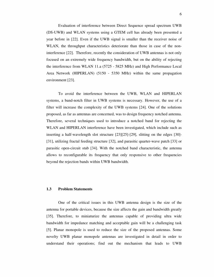
14
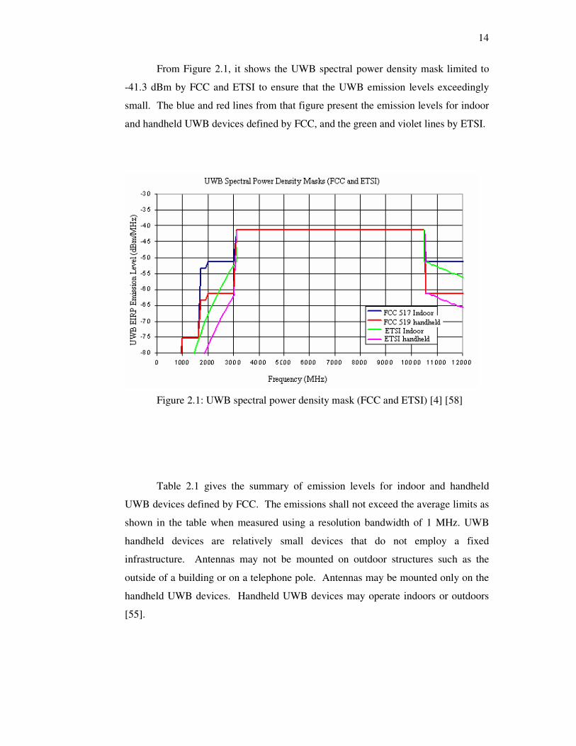
From Figure 2.1, it shows the UWB spectral power density mask limited to
-41.3 dBm by FCC and ETSI to ensure that the UWB emission levels exceedingly
small. The blue and red lines from that figure present the emission levels for indoor
and handheld UWB devices defined by FCC, and the green and violet lines by ETSI.
Figure 2.1: UWB spectral power density mask (FCC and ETSI) [4] [58]
Table 2.1 gives the summary of emission levels for indoor and handheld
UWB devices defined by FCC. The emissions shall not exceed the average limits as
shown in the table when measured using a resolution bandwidth of 1 MHz. UWB
handheld devices are relatively small devices that do not employ a fixed
infrastructure. Antennas may not be mounted on outdoor structures such as the
outside of a building or on a telephone pole. Antennas may be mounted only on the
handheld UWB devices. Handheld UWB devices may operate indoors or outdoors
[55].
15
Table 2.1: FCC limits for indoor and handheld systems [55]
Frequency (MHz) Indoor EIRP (dBm) Handheld EIRP (dBm)
960-1.610 -75.3 -75.3
1.610-1.990 -53.3 -63.3
990-3.100 -51.3 -61.3
3.100-10.600 -41.3 -41.3
Above 10.600 -51.3 -61.3
The fractional bandwidth is measured at -10 dB points on either side of the
peak emission. If these upper and lower frequencies are represented by fH and fL,
respectively, the fractional bandwidth (BW) and center frequency (fC) can be
expressed as [55]:
( ) ( )LHLH ffffBW +−= 2 (2.1)
( ) 2LHC fff += (2.2)
This fractional bandwidth greatly exceeds that of other radio transmitters,
which are generally confined to a narrow frequency band allocated for a specific
service. As a consequence of occupying a large bandwidth, UWB devices can span a
number of bands. However, as the level of emissions from UWB is very low and
below the power floor of existing frequency users, they are able to share spectrum
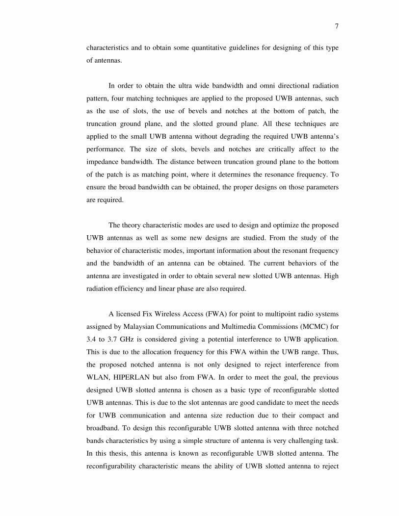
with existing services. By dividing the power of the signal across a huge frequency
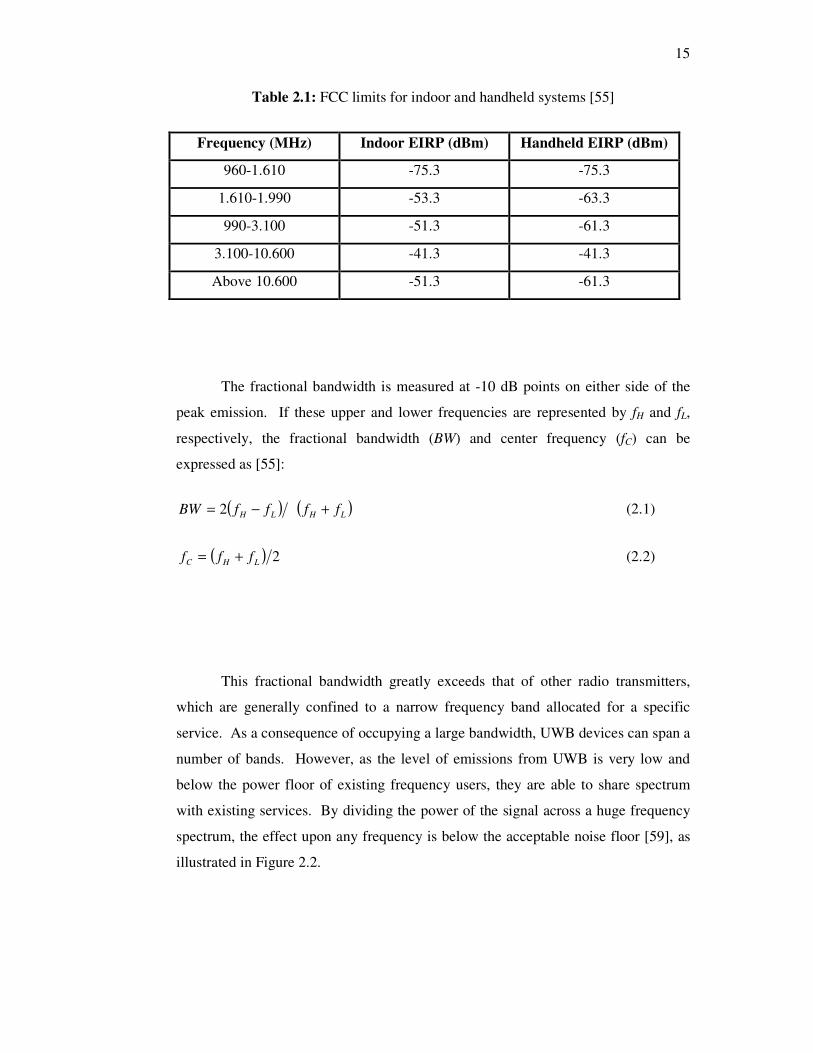
spectrum, the effect upon any frequency is below the acceptable noise floor [59], as
illustrated in Figure 2.2.
16
Figure 2.2: Ultra wideband communications spread transmitting energy across a
wide spectrum of frequency (Reproduced from [59])
The large transmission bandwidth, from near direct current (dc) to a few
GHz, has as result a higher immunity to interference effects and improved multipath
fading robustness. Another direct consequence of the large bandwidth is the
possibility to accommodate many users, even in multipath environments.
Furthermore, the very low frequencies have good penetration properties through
different materials, improving the coverage of the UWB radios.
UWB radio, operating with extremely large bandwidths, must coexist with
many other interfering narrow-band signals (TV, GSM, UMTS, GPS, etc.). In the
same time, these narrow-band systems must not suffer intolerable interference from
the UWB radios. Regulatory considerations over such a wide bandwidth limit the
radiated power. The low transmit power levels together with the ultra-fine time
resolution of the system can increase considerably the synchronization acquisition
time and the complexity of the receiver.
17
2.2.1 Regulations Worldwide
The regulatory bodies outside U.S. are also actively conducting studies to
reach a decision on the UWB regulations now. They are heavily influenced by the
FCC's decision, but will not necessarily fully adopt the FCC's regulations. In Europe,
the Electronic Communications Committee (ECC) of the Conference of European
Posts and Telecommunications (CEPT) completed the draft report on the protection
requirement of radio communication systems from UWB applications [60]. In
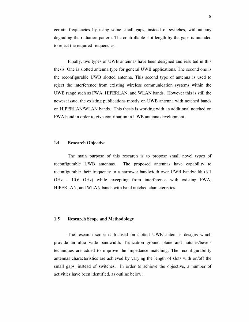
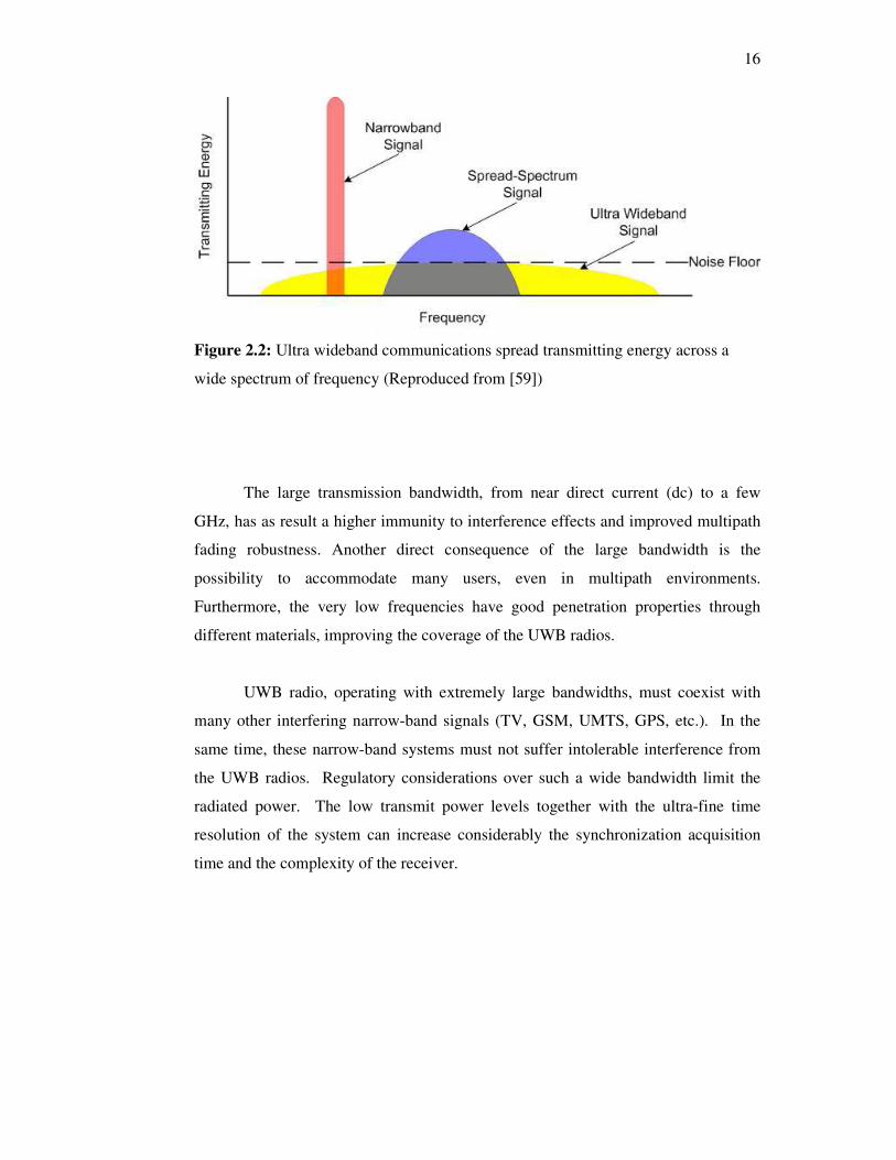
contrast to the FCC's single emission mask level over the entire UWB band, this
report proposed two sub-bands with the low band ranging from 3.1 GHz to 4.8 GHz
and the high band from 6 GHz to 8.5 GHz, respectively. The emission limit in the
high band is -41.3 dBm/MHz.
In order to ensure co-existence with other systems that may reside in the low
band, the ECC's proposal includes the requirement of Detect and Avoid (DAA)
which is an interference mitigation technique [61]. The emission level within the
frequency range from 3.1 GHz to 4.2 GHz is -41.3 dBm/MHz if the DAA protection
mechanism is available. Otherwise, it should be lower than -70 dBm/MHz. Within
the frequency range from 4.2 GHz to 4.8 GHz, there is no limitation until 2010 and
the mask level is -41.3 dBm/MHz. The ECC proposed mask against the FCC one are
plotted in Figure 2.3.
Figure 2.3: Proposed spectral mask of ECC [61]
18
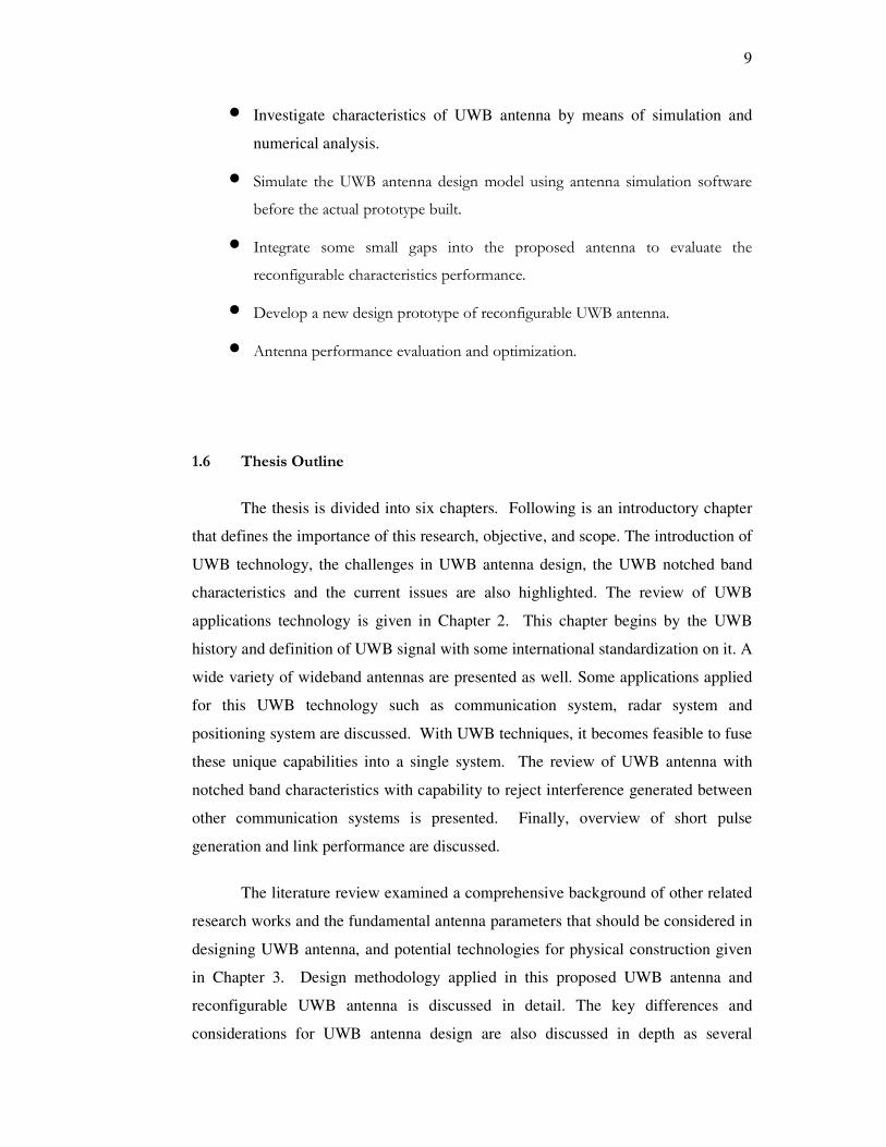
In Japan, the Ministry of Internal Affairs & Communications (MIC)
completed the proposal draft in 2005 [62]. Similar to ECC, the MIC proposal has two
sub-bands, but the low band is from 3.4 GHz to 4.8 GHz and the high band from 7.25
GHz to 10.25 GHz. DAA protections is also required for the low band.
In Korea, Electronics and Telecommunications Research Institute (ETRI)
recommended an emission mask at a much lower level than the FCC spectral mask.
Currently in Singapore the Infocomm Development Authority (IDA) permits
UWB with a special experimental license. The UWB Friendly Zone (UFZ) is
located within Science Park II, amidst the research, development, and engineering
community in Singapore [55].
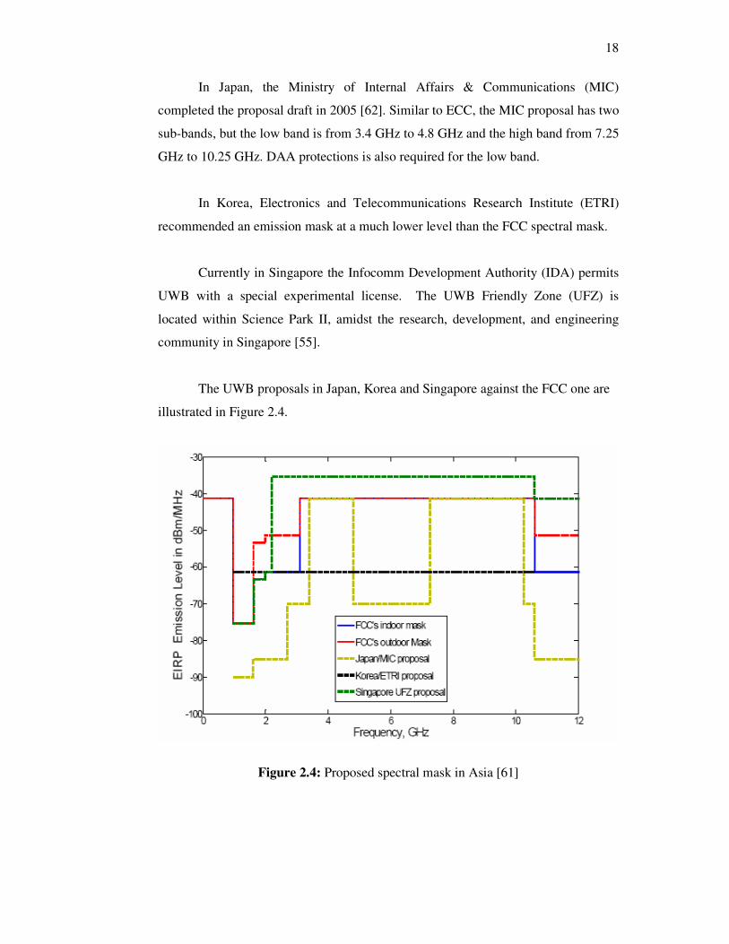
The UWB proposals in Japan, Korea and Singapore against the FCC one are
illustrated in Figure 2.4.
Figure 2.4: Proposed spectral mask in Asia [61]
19
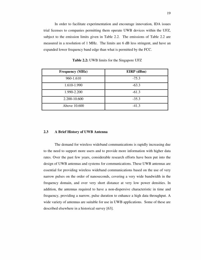
In order to facilitate experimentation and encourage innovation, IDA issues
trial licenses to companies permitting them operate UWB devices within the UFZ,
subject to the emission limits given in Table 2.2. The emissions of Table 2.2 are
measured in a resolution of 1 MHz. The limits are 6 dB less stringent, and have an
expanded lower frequency band edge than what is permitted by the FCC.
Table 2.2: UWB limits for the Singapore UFZ
Frequency (MHz) EIRP (dBm)
960-1.610 -75.3
1.610-1.990 -63.3
1.990-2.200 -61.3
2.200-10.600 -35.3
Above 10.600 -41.3
2.3 A Brief History of UWB Antenna
The demand for wireless wideband communications is rapidly increasing due
to the need to support more users and to provide more information with higher data
rates. Over the past few years, considerable research efforts have been put into the
design of UWB antennas and systems for communications. These UWB antennas are
essential for providing wireless wideband communications based on the use of very
narrow pulses on the order of nanoseconds, covering a very wide bandwidth in the
frequency domain, and over very short distance at very low power densities. In
addition, the antennas required to have a non-dispersive characteristic in time and
frequency, providing a narrow, pulse duration to enhance a high data throughput. A
wide variety of antennas are suitable for use in UWB applications. Some of these are
described elsewhere in a historical survey [63].
20
Before the decade 1990‘s, all proposed UWB antennas were based on general
volumetric and partly on planar structures [64]. Basic wideband antenna structures
have been investigated in 1939. Carter investigated biconical antenna and conical
monopole by incorporating a tapered feed. Carter was among the first to take the key
step of incorporating a broadband transition between a feed-line and radiating
elements [65]-[66].
Stratton and Chu [67]-[68] proposed the spheroidal antenna in 1941. The
spheroidal antenna was obtained by a straightforward solution of Maxwell’s
equation. The zero reactance occurs when the antenna length is slightly less than a
half wavelength for long thin wires. However, for thicker wires zero reactance may
occur when the antenna length is greater than a half wavelength, thus makes the
impedance curve broader and wider bandwidth.
In 1943 Schelkunoff proposed a biconical antenna, which presented
analytical formulas for antenna impedance characteristics for several antenna shapes.
The biconical antenna concept is based on the fact that thicker wire provides wider
impedance bandwidth that that for a thin wire dipole antenna [69]. If the biconical
antenna is flared out to infinity called as infinite biconical antenna, while the finite
biconical antenna is formed by finite sections of the two infinite cones. This antenna
is still widely used for wideband antenna applications and its variations, including
the discone antenna and the bow-tie antenna, are popular antennas for wideband
applications.
In 1947, a wideband antenna concept was proposed by the staff of the U.S.
Radio Research Laboratory at Harvard University [70]. The concept of a wideband
antenna evolves from a transmission line that gradually diverges while keeping the
inner and outer conductors ratio constant. Several variations of the concept were
developed, such as the teardrop antenna, sleeve antenna and inverted trapezoidal
antenna.
21
However, those antennas mentioned above are large, non-planar and
physically obtrusive, and therefore ruling them out as a possibility for use with small
UWB integrated electronics [71]. Currently modern telecommunication systems
require antennas with wider bandwidth and smaller dimensions than conventionally
possible.
Comparison study between the UWB antennas with conventional antennas
has been done in [8]. In that paper, the authors described a study of conventional
antennas and why they are not suitable for a UWB system. One of the simplest
practical resonant antennas is the dipole antenna. The antenna can only radiate
sinusoidal waves on the resonant frequency. Thus, the dipole antennas are not
suitable for UWB system. On the other hand, a non-resonant antenna can cover a
wide frequency range, but special care must be taken in antenna design to achieve
sufficient antenna efficiency. Moreover, the physical size of available non-resonant
antenna is inappropriate for portable UWB devices. Even with appropriate size and
sufficient efficiency, until now non-resonant antennas have not been suitable for
UWB systems [8].
In 1950’s, the spiral antennas were introduced in the class of frequency
independent antennas. These Antennas whose mechanical dimensions are short
compared to the operating wavelength is usually characterized by low radiation
resistance and large reactance [72]. Due the effective source of the radiated fields
varies with frequency, these antennas tend to be dispersive. The equiangular spiral
and archimedean spiral antennas are the most well known spiral antennas. Spiral
antennas have about a 10:1 bandwidth, providing circular polarization in low profile
geometry [73].
Transverse electric magnetic (TEM) horns and frequency-independent
antennas feature very broad well-matched bandwidths and have been widely studied
and applied [74]–[80]. However, for the log-periodic antennas structures, such as
planar log-periodic slot antennas, bidirectional log-periodic antennas, and log-
periodic dipole arrays, frequency-dependant changes in their phase centers severely
distort the waveforms of radiated pulses [81]. Biconical antennas are the earliest
antennas used in wireless systems relatively stable phase centers with broad well-
22
matched bandwidths due to the excitation of TEM modes. The cylindrical antennas
with resistive loading also feature broadband impedance characteristics [82]–[84].
However, the antennas mentioned above are seldom used in portable devices due to
their bulky size or directional radiation, although they are widely used in
electromagnetic measurements [16].
In 1982, R.H. Duhamel invented the sinuous antenna, which provides dual
linear polarization plus wide bandwidth in a compact, low profile geometry [85]. The
sinuous antenna is more complicated than the spiral antenna. However, it provides
dual orthogonal linear polarizations so that it can be used for polarization diversity or
for transmit/receive operation.
From 1992, several microstrip, slot and planar monopole antennas with
simple structure have been proposed [14][86]-[89]. They produce very wide
bandwidth with a simple structure such as circular, elliptical or trapezoidal shapes.
The radiating elements are mounted orthogonal to a ground plane and are fed by a
coaxial cable. The large ground plane mounted orthogonal to the patch made these
antennas bulkier and are difficult to fit into small devices. On the other hand,
research works on monopole and dipole UWB antennas in radiation and reception
mode for some set of operation conditions including traveling and standing wave of
exciting and induced currents in antenna was also reported in [90]. Some theoretical
and experimental generalized data are obtained. The obtained theoretical is the more
adequate approach to estimate performances of the UWB antennas in contrast to
frequency domain technique due physical nature of solving problems.
A novel UWB antenna with combination of two antenna concepts: a slot-line
circuit board antenna and a bowtie horn were introduced in 1992 [11]. These two
antenna concepts are put together to form a novel antenna type that is wide band with
easily controllable E- and H- plane beam-widths. The bowtie horn is known for its
broadband radiation pattern; whereas, the slot-line antenna provides a broadband and
balanced feed structure. However, a broadband balun is needed for the transition
between the microstrip and slotline transmission line. The microstrip and slotline are
23
on opposite sides of the substrate. Proper design of broadband balun is crucial to
improve the antenna bandwidth.
In 1998, Guillanton et al [13] proposed a new balanced antipodal vivaldi
antenna for UWB application. The author extended the tapers of the balanced
antipodal vivaldi to make the vivaldi antenna works as a dipole in lower frequency
where the slot can not radiate to extend low frequency limit. However, the bandwidth
of the antenna is limited by the transition from the feed line to the slot line of the
antenna.
In 1999, the Foursquare antenna was invented and patented by Virginia Tech
Antenna Group (VTAG). Even though this antenna does not offer as much
bandwidth as other elements, it has its unique characteristics such as unidirectional
pattern, dual polarization, low profile and compact geometry [91]-[92]. The compact
geometry of the Foursquare antenna is one of a desirable feature for wide scan,
phased array antenna.
In 2003, the trend in UWB antenna was to design notched band antennas
[25]. This antenna made insensitive to particular frequencies. This technique is useful
for creating UWB antennas with narrow frequency notches, or for creating multi-
band antenna. Since then, many researchers extended their research to investigate the
possibility interference between UWB system and existing wireless communication
systems such as HIPERLAN/WLAN systems. The commonly technique used is
adding a half wavelength slot to the patch antenna. The slot is intended to reject the
required frequencies [24]-[34].
In 2004, a new UWB antenna consisting of a rectangular patch with two
steps, a single slot on the patch and a partial ground plane has been proposed in [12].
This design provides a quasi-omnidirectional UWB antenna with group delay ripple
less than 0.5 ns. The techniques used in this paper are applied as a guideline in the
design of proposed UWB antenna in this thesis. The extensive investigation on the
effect of slot to the impedance bandwidth has been done since this issue did not
24
discussed in detail. Other research projects on UWB antenna have been reported in
[6][71][8][15][5].
In 2007, evaluation of interference between DS-UWB and WLAN using a
GTEM cell has been proposed in [22]. In 2008, the researchers extend their research
to evaluate the interference between MB-OFDM UWB and WLAN. As a result, even
if the UWB signal smaller than the receiver noise of WLAN the interference still
exist. Until 2008, hundreds of paper presenting UWB antenna design and
development are available in many international journals and conferences and some
of them as listed in this thesis’ references.
2.4 Application of UWB Technology
UWB is the leading technology for freeing people from wires, enabling
wireless connection of multiple devices for transmission of video, audio and other
high bandwidth data. Designed for short range, WPAN, it is used to relay data from a
host device to other devices in the immediate area (up to 10 m or 30 feet).
Recent years, rapid developments have been experimented on the technology
using UWB signals. UWB technology offer major enhancements in three wireless
application areas: communications, radar and positioning or ranging. UWB
technology can be delivered also over wire lines and cables such as cable television
(CATV) application. Each of these applications illustrates the unique value of UWB
[1].
2.4.1 Communication Systems
Using UWB techniques and the available large RF bandwidths, UWB
communication links has become feasible. The exceptionally large available
bandwidth is used as the basis for a short-range wireless local area network with data
25
rates approaching gigabits per second. This bandwidth is available at relatively low
frequencies thus the attenuation due to building materials is significantly lower for
UWB transmissions than for millimeter wave high bandwidth solutions. By
operating at lower frequencies, path losses are minimized and the required emitted
power is also reduced to achieve better performance.
UWB radios operate in the presence of high levels of interference by trading
data rate for processing gain. The attributes of low emitted power and wide signal
bandwidth result in a very low spectral power density of the UWB signal. This
means that UWB radios operate in the same spectrum space as narrowband radios on
a non-interfering basis. Computer peripherals offer another fitting use of UWB,
especially when mobility is important and numerous wireless devices are utilized in a
shared space. A mouse, keyboard, printer, monitor, audio speakers, microphone,
joystick, and PDA are in wireless, all sending messages to the same computer from
anywhere in the given range [55].
UWB also is used as the communication link in a sensor network. A UWB
sensor network frees the patient from the tangle of wired sensors. Sensors are being
used in medical situation to determine pulse rate, temperature, and other critical life
signs. UWB is used to transport the sensor information without wires, but also
function as a sensor of respiration, heart beat, and in some instance for medical
imaging.
UWB pulses are used to provide extremely high data rate performance in
multi-user network applications. These short duration waveforms are relatively
immune to multipath cancellation effects as observed in mobile and in-building
environments. Multipath cancellation occurs when a strong reflected wave arrives
partially or totally out of phase with the direct path signal, causing a reduced
amplitude response in the receiver. With very short pulses, the direct path has come
and gone before the reflected path arrives and no cancellation occurs. As a
consequence, UWB systems are particularly well suited for high-speed multimedia,
mobile wireless applications. In addition, because of the extremely short duration
waveforms, packet burst and time division multiple access (TDMA) protocols for
multi-user communications are readily implemented [38].
26
2.4.2 Radar Systems
For radar applications, these short pulses provide very fine range resolution
and precision distance and positioning measurement capabilities. The very large
bandwidth translates into superb radar resolution, which has the ability to
differentiate between closely spaced targets. This high resolution is obtained even
through lossy media such as foliage, soil and wall and floor of the buildings. Other
advantages of UWB short pulses are immunity to passive interference (rain, fog,
clutter, aerosols, etc) and ability to detect very slowly moving or stationary targets
[37]. UWB antennas arrays are especially important, to have both fine range and
angular resolution in radars.
In radar cross-section (RCS) range, a single UWB antenna replaces a large set
of narrow band antennas that are normally used to cover the whole frequency band of
interest. UWB signals enable inexpensive high definition radar. Radar will be used
in areas currently unthinkable such as; automotive sensors, smart airbags, intelligent
highway initiatives, personal security sensors, precision surveying, and through-the
wall public safety application [55].
Operation of vehicular radar in the 22 to 29 GHz band is permitted under the
UWB rules using directional antennas on automobiles. These devices are able to
detect the location and movement of the objects near a vehicle, enabling features
such as near collision avoidance, improved air bag activation, and suspension
systems that better respond to road conditions [55].
2.4.3 Positioning Systems
For Global Positioning System (GPS), location and positioning require the
use of time to resolve signals that allow position determination to within ten of
meters. Greater accuracy is enhanced with special techniques used. Since there is a
direct relationship between bandwidth and precision, therefore increasing bandwidth
will also increase positional measurement precision, with UWB techniques
27
extremely fine positioning becomes feasible, e.g., sub -centimeter and even sub-
millimeter [38]. In satellite communications where wide band feeds save space and
weight by supporting many communication channels with just one antenna.
The architectures for UWB position-determination systems would resemble
traditional systems, e.g. multi-alterations like GPS or radio ranging like the military’s
Enhanced Position Location and Reporting System (EPLRS). Having relatively low
frequency of operation, this type of system has the potential to work within buildings
with minimal attenuation of the signal.
With UWB techniques, it becomes feasible to fuse these unique capabilities
into a single system. Thus, it is possible to create communications systems in which
position is determined to within less than a centimeter. Moreover, it is possible to
build radars (proximity sensors) that communicate simultaneously. Since UWB
exhibits all of these characteristics while allowing spectrum bandwidths to be re-use
and maintain that little or no interference to be generated between other
communication systems. Therefore, the emission of UWB will greatly boost the
performance of intrusion detection radar precision geo-location systems, proximity
fuses and secure ground communications for troops which far outweigh the impact of
UWB may have on other systems.
2.4.4 UWB over Wires
UWB technology is also delivered over wire lines and cables. This could
effectively double the bandwidth available to CATV systems without modification to
the existing infrastructure. Over wire technology for coaxial cable provide up to 1.2
Gbps down-stream and up to 480 Mbps upstream of additional bandwidth, at low
cost, on differing CATV architectures. The wire-line UWB technology does not
interfere with or degrade television, high speed internet, voice or other services
already provided by the CATV infrastructure [55].
28
2.5 Short-Pulse Generation
UWB technology involves the radiation, reception and processing of very wide
bandwidth radio frequency emissions. The main reason for such high bandwidths is
that UWB devices send out tiny bursts of radio signals over many frequencies. Data
goes out in millions of pulses per second and is re-assembled by a receiving UWB
device. These bursts represent from one to only a few cycles of an RF carrier wave.
The resultant waveforms are extremely broadband, it is often difficult to determine an
actual RF center frequency thus, the term "carrier-free". Most other wireless
technologies use a single radio frequency carrier.
In general, UWB radio systems transmit and receive single band (SB) or
multi-band (MB) pulses. SB based, employing one single transmission frequency
band, and MB based, employing two or more frequency bands, each with at least 500
MHz bandwidth.
In the SB solution, the UWB signal is generated using very short, low duty-
cycle, baseband electrical pulses with appropriate shape and duration. Due to the
carrier-less characteristics, no sinusoidal carrier to raise the signal to a certain
frequency band, these UWB systems are also referred to as carrier-free or impulse
radio (IR-UWB) communication systems [93]. Such systems are capable of
providing low system complexity and low cots because of their direct transmission
and reception of pulsed signals and the least RF devices in their front-ends as against
conventional narrow-band radio systems [5].
The MB UWB systems is implemented carrier less (different pulse
shapes/lengths are used according to the frequency band) [36] or carrier based
(multi-carrier like) [94] known as UWB-OFDM. In UWB-OFDM bandwidth is split
into many sub-bands applying communication techniques well-known from
narrowband systems.
The requirements for UWB antennas can vary for different schemes. In the
multiband scheme, the consistent or flat gain response of the UWB antennas is more
important than a constant group delay or a linear phase response, which is conversely
more important in the single band scheme. Therefore, the performance of UWB
29
antennas can be assessed in terms of the system transfer function and group delay
together with conventional frequency-domain parameters such as return loss, gain,
radiation patterns, and polarization matching path loss as well as the time-domain
parameters such as pulse waveforms, and fidelity [16].
In the IR UWB solutions, typically the radiated pulse signals are generated
without the use of local oscillators or mixers, thus potentially a simpler and cheaper
construction of the transmitter (TX) and receiver (RX) is possible, as compared to
the conventional narrow-band systems. The characteristics of the pulse used (shape,
duration), determine the bandwidth and spectral shape of the UWB signals. The
most common pulse shapes used in IR-UWB are: Gaussian monocycle (and its
derivatives) and Hermitian pulses [95].
The impulse radio technology has been widely used in radar applications due
to its spatial resolution, detectable material penetration, easy target detection and
feature extraction and low probability of intercept signals [96]-[98]. Military and
government multi-user networking and high precision localization applications rely
on the UWB communication systems [99].
The basic properties of the impulse radio systems make the UWB technology
ideal candidate also for commercial, short-range, low power, low cost indoor
communication systems such as WLAN and WPAN [100]-[102].
2.6 UWB Link Performance
As with narrowband antennas, the link behavior of UWB antennas in free
space is governed by Friis’s Law [79]:
22
2
2
2
)4()4( fr
cGGP
r
GGPP RXTX
TX
RXTX
TXRXππ
λ== (2.3)
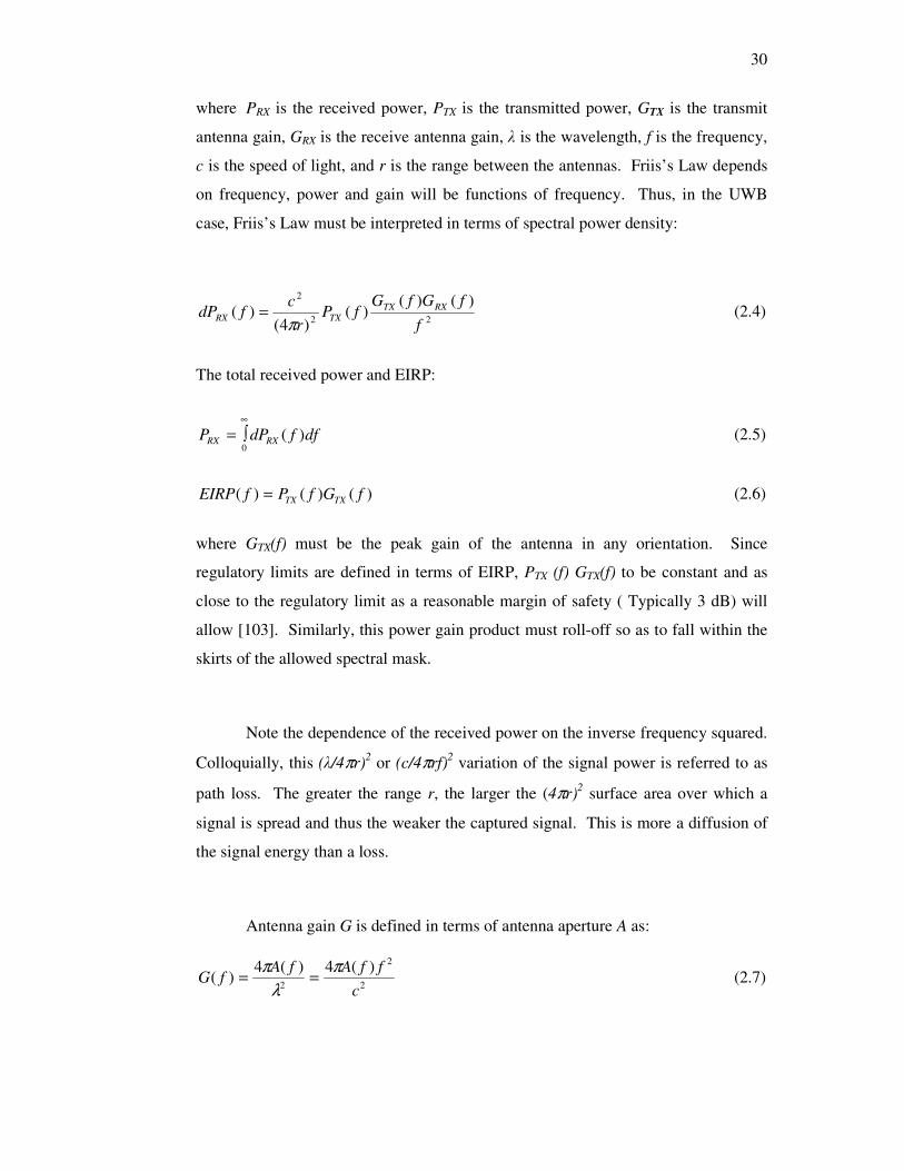
30
where PRX is the received power, PTX is the transmitted power, GTX is the transmit
antenna gain, GRX is the receive antenna gain, λ is the wavelength, f is the frequency,
c is the speed of light, and r is the range between the antennas. Friis’s Law depends
on frequency, power and gain will be functions of frequency. Thus, in the UWB
case, Friis’s Law must be interpreted in terms of spectral power density:
22
2 )()()(
)4()(
f
fGfGfP
r
cfdP RXTX
TXRXπ
= (2.4)
The total received power and EIRP:
dffdPP RXRX )(0
∞
∫= (2.5)
)()()( fGfPfEIRP TXTX= (2.6)
where GTX(f) must be the peak gain of the antenna in any orientation. Since
regulatory limits are defined in terms of EIRP, PTX (f) GTX(f) to be constant and as
close to the regulatory limit as a reasonable margin of safety ( Typically 3 dB) will
allow [103]. Similarly, this power gain product must roll-off so as to fall within the
skirts of the allowed spectral mask.
Note the dependence of the received power on the inverse frequency squared.
Colloquially, this (λ/4πr)2 or (c/4πrf)
2 variation of the signal power is referred to as
path loss. The greater the range r, the larger the (4πr)2 surface area over which a
signal is spread and thus the weaker the captured signal. This is more a diffusion of
the signal energy than a loss.
Antenna gain G is defined in terms of antenna aperture A as:
2
2
2
)(4)(4)(
c
ffAfAfG
π
λ
π== (2.7)
31
This antenna aperture is the effective area of the antenna, a measure of how
big a piece of an incoming wave front an antenna can intercept. For directive,
electrically large antennas, antenna aperture tends to be comparable to the physical
area. For omni directional small element antennas, the antenna aperture may actually
be significantly larger than the antennas’s physical area. This follow from the ability
of electromagnetic waves to couple to objects within about λ/2π.
2.7 Summary
In this chapter, a brief history of UWB antenna technology has been reviewed.
From the literature reviews, the UWB antenna concept has been investigated since
many decades. The FCC released the regulations of UWB technology for
commercial purposed since 2002. The standardizations or regulation applied for this
technology in Europe and Asia with their specific requirements is also presented in
detail. These regulations are used as guidelines for research work. The frequency
bands were allocated based on certain applications. Some applications with their
signal characteristics and performance link are discussed. Overview of UWB short
pulse and link performance are also given. The contents of this chapter have been
published as a full paper in the fifth international conference on wireless and optical
communication networks (WOCN 2008).
32
CHAPTER 3
ULTRA WIDEBAND ANTENNA DESIGN METHODOLOGY
3.1 Introduction
For many years, the idea of an UWB antenna that would allow stable pattern
control over many frequency decades seemed elusive at the best. UWB antennas
require the phase center and voltage standing wave ratio (VSWR) to be constant
across the whole bandwidth of operation. A change in phase center may cause
distortion on the transmitted pulse and worse performance at the receiver. The
antennas are significant pulse-shaping filters. Any distortion of the signal in the
frequency domain (filtering) causes distortion of the transmitted pulse shape, thereby
increasing the complexity of the detection mechanism at the receiver [104]. As
discussed in Chapter 1, monopole antennas match most these characteristics
representing the starting point of the modern research on broadband antenna [14].
Accordingly, many techniques to broaden the impedance bandwidth of small
antennas and to optimize the characteristics of broadband antennas have been widely
investigated. Detail discussion on various bandwidth enhancement techniques will
further examined in section 3.3.
The reduction in antenna size presents various problems due to the
performance penalties in antenna characteristics, such as impedance, efficiency, and
bandwidth. Small antennas are defined as those which have smallness in terms of
size, wavelength, and function, and they are divided into four categories [105]. The
first is electrically small antennas, which have a very small size compared to the
33
wave length (λ). The second is physically constrained small antennas, which are not
necessary electrically small, but are shaped in such a way that considerable size
reduction is achieved in one plane. The third is physically small antennas, which
have dimensions regarded as small in a relative sense. The last is functionally small
antennas, which are antenna systems that achieved additional functions without
increasing size [105].
In this thesis, the proposed slotted UWB antennas meet those four categories
as a small antenna. Their sizes are less than a wavelength, compact size in one plane,
considerable smaller size compared to the antennas sizes in the references listed
[12][16][106][107]-[108][109]-[111][112], and suitable for many UWB applications.
Comparison in terms of antenna sizes between the proposed antennas and several
UWB antennas listed in the references has been done. Those proposed antennas
originate from conventional rectangular monopole and are realized by adding slots
for both patch and feeding strip.
In order to understand the challenges that UWB provides to antenna’s
designer, a comprehensive background outlining several characterizing antenna
parameters will be presented. Next, a clear description of various bandwidth
enhancement techniques that required in the design of UWB antennas is presented.
Some related research works are reviewed as well. Several techniques that employed
in the design reconfigurable UWB antenna with band notched characteristic will be
further discussed. Fundamental antenna parameters must be fully defined and
explained before a thorough understanding of antenna requirements for a particular
application can be achieved.
3.2 Fundamental Antenna Parameter
An antenna is a transducer that converts guided electromagnetic energy in a
transmission line to radiate electromagnetic energy in free space. The fundamental
principles of an antenna design are based on electromagnetic field theory. An
antenna working condition depends on the antenna parameters. These factors will
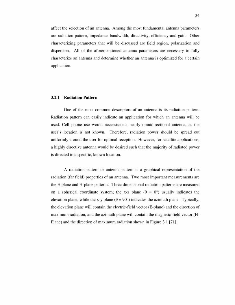
34
affect the selection of an antenna. Among the most fundamental antenna parameters
are radiation pattern, impedance bandwidth, directivity, efficiency and gain. Other
characterizing parameters that will be discussed are field region, polarization and
dispersion. All of the aforementioned antenna parameters are necessary to fully
characterize an antenna and determine whether an antenna is optimized for a certain
application.
3.2.1 Radiation Pattern
One of the most common descriptors of an antenna is its radiation pattern.
Radiation pattern can easily indicate an application for which an antenna will be
used. Cell phone use would necessitate a nearly omnidirectional antenna, as the
user’s location is not known. Therefore, radiation power should be spread out
uniformly around the user for optimal reception. However, for satellite applications,
a highly directive antenna would be desired such that the majority of radiated power
is directed to a specific, known location.
A radiation pattern or antenna pattern is a graphical representation of the
radiation (far field) properties of an antenna. Two most important measurements are
the E-plane and H-plane patterns. Three dimensional radiation patterns are measured
on a spherical coordinate system; the x-z plane (θ = 0°) usually indicates the
elevation plane, while the x-y plane (θ = 90°) indicates the azimuth plane. Typically,
the elevation plane will contain the electric-field vector (E-plane) and the direction of
maximum radiation, and the azimuth plane will contain the magnetic-field vector (H-
Plane) and the direction of maximum radiation shown in Figure 3.1 [71].
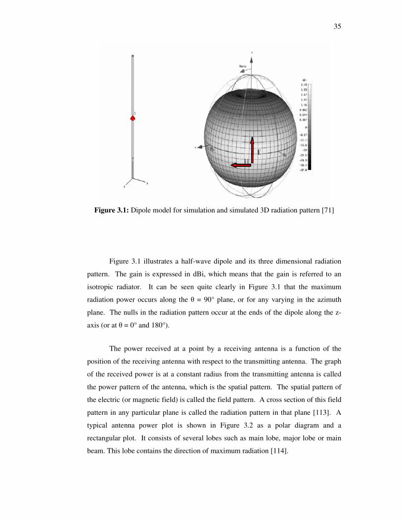
35
Figure 3.1: Dipole model for simulation and simulated 3D radiation pattern [71]
Figure 3.1 illustrates a half-wave dipole and its three dimensional radiation
pattern. The gain is expressed in dBi, which means that the gain is referred to an
isotropic radiator. It can be seen quite clearly in Figure 3.1 that the maximum
radiation power occurs along the θ = 90° plane, or for any varying in the azimuth
plane. The nulls in the radiation pattern occur at the ends of the dipole along the z-
axis (or at θ = 0° and 180°).
The power received at a point by a receiving antenna is a function of the
position of the receiving antenna with respect to the transmitting antenna. The graph
of the received power is at a constant radius from the transmitting antenna is called
the power pattern of the antenna, which is the spatial pattern. The spatial pattern of
the electric (or magnetic field) is called the field pattern. A cross section of this field
pattern in any particular plane is called the radiation pattern in that plane [113]. A
typical antenna power plot is shown in Figure 3.2 as a polar diagram and a
rectangular plot. It consists of several lobes such as main lobe, major lobe or main
beam. This lobe contains the direction of maximum radiation [114].
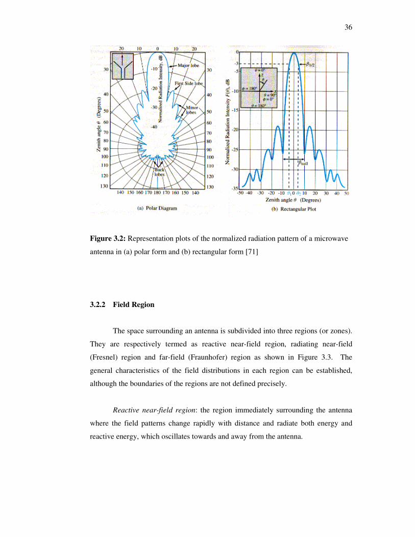
36
Figure 3.2: Representation plots of the normalized radiation pattern of a microwave
antenna in (a) polar form and (b) rectangular form [71]
3.2.2 Field Region
The space surrounding an antenna is subdivided into three regions (or zones).
They are respectively termed as reactive near-field region, radiating near-field
(Fresnel) region and far-field (Fraunhofer) region as shown in Figure 3.3. The
general characteristics of the field distributions in each region can be established,
although the boundaries of the regions are not defined precisely.
Reactive near-field region: the region immediately surrounding the antenna
where the field patterns change rapidly with distance and radiate both energy and
reactive energy, which oscillates towards and away from the antenna.
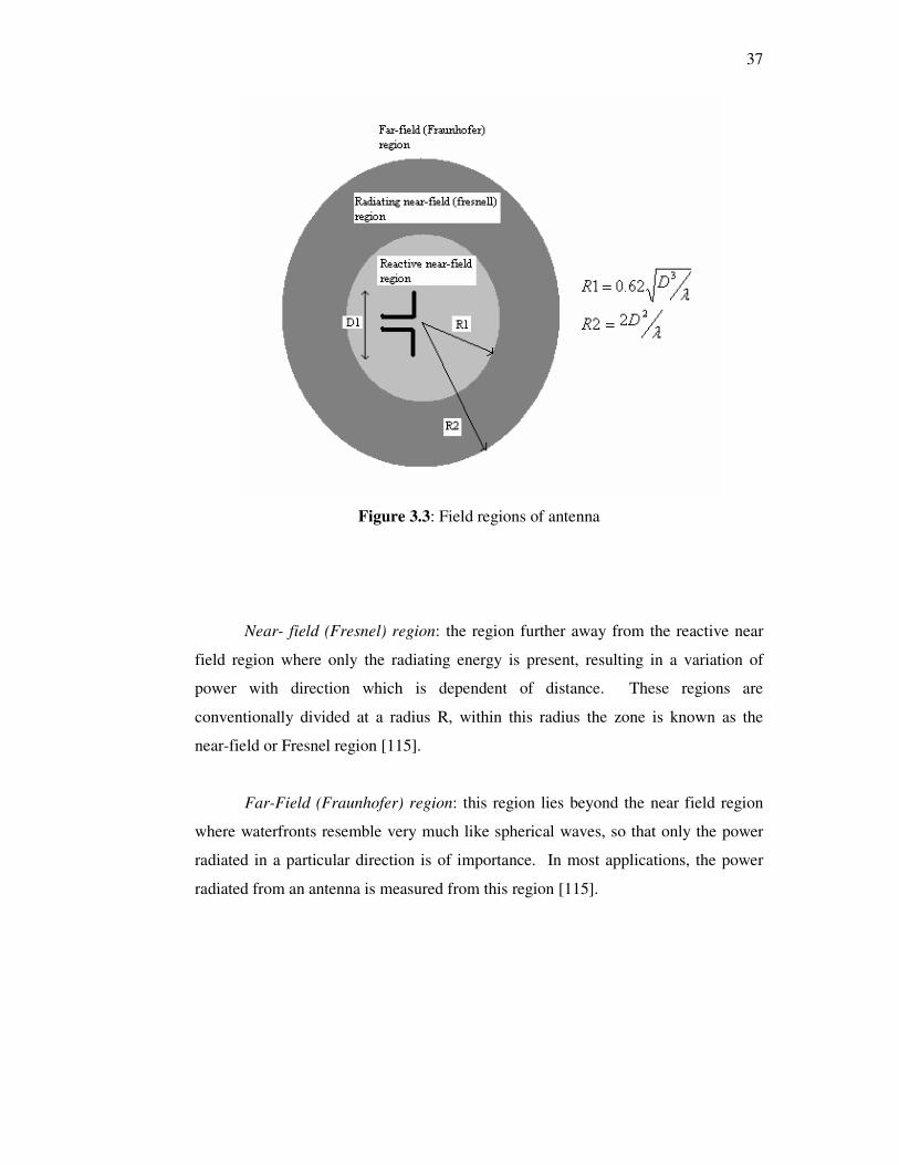
37
Figure 3.3: Field regions of antenna
Near- field (Fresnel) region: the region further away from the reactive near
field region where only the radiating energy is present, resulting in a variation of
power with direction which is dependent of distance. These regions are
conventionally divided at a radius R, within this radius the zone is known as the
near-field or Fresnel region [115].
Far-Field (Fraunhofer) region: this region lies beyond the near field region
where waterfronts resemble very much like spherical waves, so that only the power
radiated in a particular direction is of importance. In most applications, the power
radiated from an antenna is measured from this region [115].
38
3.2.3 Directivity, Efficiency and Gain
Directivity is how much an antenna concentrates energy in one direction in
preference to radiation in other directions. It is equal to its power gain if the antenna
is 100% efficient, which means that it is a perfect antenna that radiates equally in all
directions. This antenna is called an isotropic radiator. Power gain is expressed
relative to a reference such as isotropic radiator or half-wavelength dipole. Since all
real antennas will radiate more in some directions than in others, therefore the gain is
the amount of power that can achieve in one direction at the expense of the power
lost in the others [63]. Gain is always related to the main lobe and is expressed in
dBi or dBd.
The antenna efficiency takes into consideration the ohmic losses of the antenna
through the dielectric material and the reflective losses at the input terminals. Reflection
efficiency and radiation efficiency are both taken into account to define total antenna
efficiency. Reflection efficiency, or impedance mismatch efficiency, is directly
related to the S11 parameter (Γ). Reflection efficiency is indicated by er, and is
defined mathematically as follows:
[ ]( )21 Γ−=re (3.1)
The radiation efficiency takes into account the conduction efficiency and
dielectric efficiency, and is usually determined experimentally with several
measurements in an anechoic chamber. Radiation efficiency (erad) is determined by
the ratio of the radiated power, Prad to the input power at the terminals of the antenna,
Pin:
in
radrad
P
Pe = (3.2)
Total efficiency is simply the product of the radiation efficiency and the
reflection efficiency. Reasonable values for total antenna efficiency are within the
39
range of 60% - 90%, although several commercial antennas achieve only about 50%
- 60% due to inexpensive, lossy dielectric materials such as FR4.
The antenna gain measurement is linearly related to the directivity
measurement through the antenna radiation efficiency. Gain measurement is
typically misunderstood in terms of determining the quality of an antenna. A
common misconception is that the higher the gain, the better the antenna. This is
only true if the application requires a highly directive antenna. Since gain is linearly
proportional to directivity, the gain measurement is a direct indication of how
directive the antenna is (provided the antenna has adequate radiation efficiency).
3.2.4 Impedance Bandwidth
The Institute of Electrical and Electronic Engineers (IEEE) standard [116]
defines the bandwidth of an antenna as “the range of frequencies within which the
performance of the antenna, with respect to some characteristics, conforms to a
specific standard.” Usually the bandwidth is characterized by impedance bandwidth.
The impedance bandwidth indicates the bandwidth for which the antenna is
sufficiently matched to its input transmission line such that 10% or less of the
incident signal is lost due to reflections. Impedance bandwidth measurements
include the characterization of the VSWR and return loss throughout the band of
interest.
The impedance of an antenna is the impedance at the antenna terminals with
no load attached, impedance may be defined as the ratio of the voltage to current at
the antenna terminals or the ratio of the appropriate components of electric and
magnetic fields at a point. Maximum power transfer can only be achieved when the
impedance of the antenna is matched to those of the load, which involve complex
conjugate of the load impedance. Power reflected at the terminals of the antenna is
the main concern related to impedance matching.
40
Impedance matching has been particularly difficult to achieve in UWB
antennas, since its impedance has to remain constant over a wide spectrum of
frequencies. A good match can be achieved with careful design and employing
appropriate mechanisms, such as resistive loading [115]. A good impedance match
is indicated by a return loss greater than 10 dB.
VSWR is a measure of impedance mismatch between the transmission line
and its load. The higher the VSWR, the greater is the mismatch. The minimum
VSWR that corresponds to a perfect impedance match is unity [115]. The typically
desired value of VSWR to indicate a good impedance match is 2.0 or less. Most
radio equipment is built for an impedance of 50-ohm.
3.2.5 Polarization
Antenna polarization indicates the polarization of the radiated wave of the
antenna in the far-field region as shown in Figure 3.4. The position and direction of
the electric field with reference to the earth’s surface or ground determines wave
polarization. In general, the electric field is the same plane as the antenna's radiator.
Horizontal polarization is the electric field parallel to the ground. Vertical
polarization is the electric field perpendicular to the ground. There is one special
polarization known as Circular polarization. As the wave travels it spins to cover
every possible angle. It can either be right-handed or left-handed circular
polarization depending on which way it is spinning. Another common type of
polarization is elliptical, which is a cross between linear (horizontal or vertical) and
circular polarization.
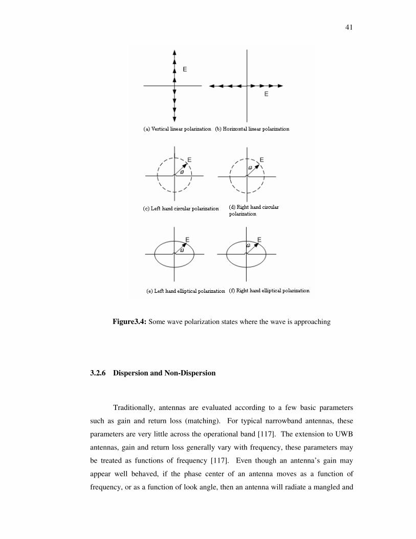
41
Figure3.4: Some wave polarization states where the wave is approaching
3.2.6 Dispersion and Non-Dispersion
Traditionally, antennas are evaluated according to a few basic parameters
such as gain and return loss (matching). For typical narrowband antennas, these
parameters are very little across the operational band [117]. The extension to UWB
antennas, gain and return loss generally vary with frequency, these parameters may
be treated as functions of frequency [117]. Even though an antenna’s gain may
appear well behaved, if the phase center of an antenna moves as a function of
frequency, or as a function of look angle, then an antenna will radiate a mangled and
42
dispersed waveform. Then UWB system must compensate for these differences.
This compensation may be difficult and resources intensive.
The half-wave dipole is a commonly used antenna in carrier based systems.
However, when a half-wave dipole pair is used for transmitting and receiving UWB
signals, it is very avoid the severe ringing and dispersion problems. These are typical
problems using narrow-band antenna to transmit and receive UWB pulses [118].
A log periodic antenna is an example of a dispersive antenna [103]. The log
periodical antenna is actually a combination of dipole antennas with different lengths
[118]. A smaller scale portion radiates high frequency components and a larger scale
portion radiates lower frequency components of a signal. Because the phase center
moves as a function of a frequency, frequency independent antennas radiate
dispersed signals. The dispersion is a problem for multi-band systems as well as
those where a radiated signal occupies the entire band [117]. This phase variation
may have a serious impact on UWB antenna performance. The best way to obtain
quick qualitative assessment of dispersion is to look at the time domain
electromagnetic field signal emitted by an antenna. In addition, a UWB antenna is
preferentially non-dispersive, having a fixed phase center.
All of the fundamental parameters described must be considered in designing
antennas for any radio application, including UWB. However, there are additional
challenges for UWB.
3.3 UWB Antenna Design Methodology
In order to fulfill the UWB antenna requirements, various bandwidth
enhancement techniques for planar monopole antennas have been developed during
last two decades. The recent trends in improving the impedance bandwidth of small
antennas can be broadly divided into the following categories [119], [16], [6], the
first category is the leading of all categories in numbers and varieties. By varying the
43
physical dimensions of the antenna, the frequency and bandwidth characteristics of
the resulting UWB pulse could be adjusted [37].
3.3.1 Various Geometries and Perturbations
Planar monopoles with a huge number of different geometries have been
numerically characterized [16]. Many techniques to broaden the impedance
bandwidth of planar monopole antennas and to optimize the characteristics of these
antennas have been widely investigated. Among all these techniques, the beveling
technique was reported to yield maximum bandwidth. Various geometries and
perturbations are used to introduce multiple resonances as well as input impedance
matching. The input impedance is also extremely dependent on the feeding gap
configuration [120].
Beveling the bottom edge of the radiating element has been demonstrated to
shift upward significantly the upper edge frequency when properly designed
[106][35][121][123]. The optimization of the shape of the planar antenna especially
the shape of the bottom portion of the antenna, improve the impedance bandwidth by
achieving smooth impedance transition [16]. In fact, this part of the radiator results to
be very critical for governing the capacitive coupling with the ground plane. Any
reshaping of this area strongly affects the current path [106]. A modal study of four
common planar monopole geometries has been performed in [120]. The election and
beveling angle is critical, as it determines the matching of the mode.
The patch radiator may be slotted to improve the impedance matching,
especially at higher frequency. The slots cut from the radiators change the current
distribution at the radiators so that the impedance at the input point and current path
change [16]. A notch is cut from radiator to reduce the size of the planar antenna
[35].
Adding a strip asymmetrically at the top of the radiator can also reduce the
height of the antenna and improve impedance matching [124].
44
An offset feeding point has been used in order to excite more modes and
consequently improving the impedance bandwidth [122]. By optimizing the location
of the feed point, the impedance bandwidth of the antenna will be further widened
because the input impedance is varied with the location of the feed point [122].
Moreover, other strategies to improve the impedance bandwidth which do not
involve a modification of the geometry of the planar antenna have been investigated.
Basically, these strategies consist of adding a shorting post to the structure or using
two feeding points to excite the antenna [120]. A shorting pin is also used to reduce
the height of the antenna [125]. In [106], the shorting pin inserted to the antenna that
provides a broad bandwidth has been investigated. A dual feed structure greatly
enhanced the bandwidth particularly at higher frequencies [126]. By means of
electromagnetic coupling (EMC) between the radiator and feeding strip, good
impedance matching can be achieved over a broad bandwidth [127].
The use of double feeding configuration to the antenna structure is to enforce
the vertical current mode, whereas it prevents other modes such as horizontal and
asymmetrical current modes from being excited, which degrade the polarization
properties and the impedance bandwidth performance of the antenna [107[128]-
[130]. The double feeding gives a significant improvement of the vertical current
distribution resulting in better matching notably over the upper-band part [108]. The
matching of this upper frequency band is mainly governed by two parameters: the
distance between the two monopole ports and the height between the monopole and
the ground plane [107]. In [129] a square monopole antenna with a double feed has
been proposed. This feed configuration has shown the improvement on radiation
pattern and impedance bandwidth. This is due to a pure and intense vertical current
distribution generated in the whole structure.
The hidden feed-line technique on printed circular dipole antenna has been
investigated in [131]. The specific feeding has shown remove any radiation pattern
disturbance generally met with this kind of antenna when fed with a coaxial or a
microstrip line. It was also shown a wide frequency bandwidth.
45
Due to the radiation from planar antenna may not be omni directional at all
operating frequencies because they are not structurally rotationally symmetrical. Roll
monopoles is a choice to feature broad impedance bandwidth with omni directional
characteristics [132]. With the roll structure, the antenna becomes more compact and
rotationally symmetrical in the horizontal plane. However, the roll monopoles are not
easy to fabricate with high accuracy [16]. The folded antenna was also presented in
[133] in order to improve radiation pattern maintaining the broadband behavior. In
[133], the antenna was analyzed employing transmission line model (TLM).
In [112], various combinations of bandwidth enhancement techniques was
successfully applied in UWB antenna design such as adding slit in one side of the
monopole, tapered transition between the monopole and the feed line, and adding
notched ground plane.
From various bandwidth enhancement techniques, there are four techniques
adopted for this proposed UWB antennas design. The four techniques are the use of
slots for both patch and feeding strip, truncation ground plane, bevels or notches at
the bottom, and notched ground plane which can lead to a good impedance
bandwidth. The original contribution focused on the various slots types design. The
proposed slotted UWB antennas are designed by adding asymmetry couple slots
without degrading their performance. The performance optimization is done by
studying their current distribution.
3.3.2 Genetic Algorithm (GA)
Optimization of patch geometry is an ideal technique to have single or more
optimized figures of merit like, impedance bandwidth. The GA has been
successfully applied by a number of researchers to improve the impedance
bandwidth [5], [134]-[138]. The optimized shape however is too much irregular and
unconventional and this can only be fabricated using the pattern produced in true
scale by the GA code.
46
Electromagnetic optimization problems generally involve a large number of
parameters. The parameters can be either continuous, discrete, or both, and often
include constraints in allowable values. The goal of the optimization is to find a
solution that represents a global maximum or minimum. For example, the
application of GA optimization is used to solve the problem of design a broadband
patch antenna [5]. Parameters that are usually included in this type of optimization
problem include the location of the feed probe, the width and length of the patch, and
the height of the patch above the ground plane. In addition, it may be desirable to
include constraints on the available dielectric materials, both in terms of thickness
and dielectric constants; tolerance limits on the patch size and probe location;
constraints on the weight of the final design; and possibly even cost constraints for
the final production model. Given the large number of parameters, and the
unavoidable mixture of discrete and continuous parameters involved in this problem,
it is virtually impossible to use traditional optimization methods. GA optimizers, on
the other hand, can readily handle such a disparate set of optimization parameters [5].
The use of the GA approach in the design of UWB antennas has been
proposed in [134]-[135]. The planar fully-metal monopole (PFMM) of bow tie (BT)
and reverse bow tie (RBT) have been demonstrated in [134], [136] have an ultra-
wide bandwidth. The element height, the feed height, and the element flare angle
were the parameters that used in optimization. The height essentially determines the
operating mode and the lower frequency limit of the antenna, while the flare angle
and the feed height control the variation of the input impedance over frequency, the
high frequency impedance value, as well as the resonance bandwidth [134]. In this
paper, the GA was used to determine the optimal dimensions of the selected element
shape in order to fulfill the given bandwidth requirement. As a result, the RBT
antenna can achieve a much wider impedance bandwidth than the BT with
significantly reduced sizes.
In [135], the semi-conical UWB antenna was optimized by using the Green’s
Function Method (GFM) Absorbing Boundary Condition (ABC) with GA. The goal
of this optimization is to have significant reduction in the size of the white space, due
to the unique capability of the GFM to model arbitrarily shaped boundaries in close
47
proximity to the antenna. The white space is defined as the region between the
antenna and the absorbing boundary.
The GA optimizer is also used to reconfigure the radiation characteristics of
antenna over an extremely wide-band [137]. The design results indicate that the
antenna can obtain the required goals over an ultra-wide band through reconfiguring
the states of the switch array installed in shared aperture when it operates with the
higher order modes [137]. Optimization of broadband and dual-band microstrip
antennas on a high-dielectric substrate by using GA was also proposed in [138].
3.3.3 Resonance Overlapping
Normally, the bandwidth of a resonant antenna is not very broad because it
has only one resonance. But if there are two or more resonant parts available with
each one operating at its own resonance, the overlapping of these multiple
resonances may lead to multi-band or broadband performance.
Theoretically, an ultra wide bandwidth can be obtained if there are a
sufficient number of resonant parts and their resonances can overlap each other well.
However, in practice, it is more difficult to achieve impedance matching over the
entire frequency range when there are more resonant parts. Also, it will make the
antenna structure more complicated and more expensive to fabricate. Besides, it is
more difficult to achieve constant radiation properties since there are more different
radiating elements.
48
3.4 Reconfigurable UWB Antenna
This section presents the concept of reconfigurable antennas and the
emerging technologies that make reconfigurable antenna possible. There are three
parameters that frequently used for designing the reconfigurable antennas such as,
frequency, polarization and radiation patterns.
3.4.1 Reconfigurability Antenna Parameters
Ideally, reconfigurable antennas should be able to alter their operating
frequencies, impedance bandwidth, polarizations, and radiation patterns
independently to accommodate operating requirements. However, the development
of these antennas posses significant challenges to both antenna and system designers.
These challenges lie not only in obtaining the desired levels of antenna functionality
but also in integrating this functionality into complete systems to arrive at efficient
and cost effective solutions.
3.4.1.1 Frequency Response Reconfigurability
Frequency reconfigurable antennas are classified into two categories:
continuous and switched [78]. Continuous frequency-tunable antennas allow for
smooth transitions within or between operating bands without jumps. Switched
tunable antennas use some kind of switching mechanism to operate at distinct and
separated frequency bands. The main differences are in the extent of the effective
length changes that enable operation over different frequency bands and the devices
to achieve these changes. There are different kinds of switching technology, such as
optical switches, PIN diodes, FETs, and radio frequency microelectromechanical
system (RF-MEMS) switches, in frequency tunable monopole antennas for various
frequency bands. The effective length of the antenna can be altered by adding or
removing these switches, hence altering its operating frequency.
49
3.4.1.2 Polarization Reconfigurability
Antenna polarization reconfiguration provides immunity to interfering signals
in varying environments as well as provides an additional degree of freedom to
improve link quality as a form of switched antenna diversity [139]. The direction of
current flow on the antenna translates directly into the polarization of the electric
field in the far field of the antenna. To achieve polarization reconfigurability, the
antenna structure, material properties, feed configuration have to change in ways that
alter the way current flows on the antenna. The main difficulty of this kind of
reconfigurability is that this must be accomplished without significant changes in
impedance or frequency characteristics [78]. The mechanisms to achieve these
modifications are the same as those described for frequency reconfigurability earlier.
3.4.1.3 Radiation Pattern Reconfigurability
Reconfigurable radiation patterns can be achieved with slot-based radiators as
presented in [140]. Both frequency and pattern reconfigurabilities are due to
incorporated the PIN diode switches into the slot radiator. Frequency
reconfigurability is supported through PIN diode switches that control input
impedance circuitry, whereas the pattern reconfigurability is enabled with diode
switches placed at locations around the slot to control the direction of a pattern null
that is inherent to basic antenna operation [78], [140]. For UWB antenna, the
reconfigurability of radiation pattern is not an important issue since it requires omni
directionality pattern over frequency bands. Next section will be further discussed on
frequency notch UWB antenna as main focused in this thesis.
50
3.4.2 Design Methodology
As mentioned previously, one way to implement a frequency notched UWB
antenna is to incorporate a half wave resonance structure in an antenna. In [25], there
are two varieties of slotted antennas which have a frequency notched reported, a
triangular notch and elliptical notch. Both antennas have frequency notch
characteristics where the arc length of slots form a half wavelength resonance
structure at particular frequency, thus a destructive interference takes place causing
the antennas to be non responsive at that frequency [25].
Other types of this kind of antenna was reported in [141], a band notched
UWB antenna using a slot-type split ring resonator (SRR) was found very effective
in rejecting unwanted frequency, such as that for WLAN service, in terms of its
selectivity and small dimension. The SRR is composed of two concentric split ring
slots and proposed for band stop application, since it provides high Q characteristic.
It is expected that the smaller structure has a relatively smaller effect on the radiation
patterns of the antenna. SRR has a favorable aspect in its size, and it can be designed
as small as one-tenth of the resonance wavelength [141]. The slotted SRR was
positioned near the feeding point to provide more coupling with the field.
A multiple band-notched planar monopole antenna using multiple U-shape
slots for multi band wireless system was presented in [142]. The half wavelength U-
shape slots were symmetrically inserted in the center of the planar element.
Therefore, in order to generate the two band-notched characteristics, three U-shape
slots were proposed. The center U-shape slot makes one notch band at 3.03 GHz and
the other two symmetric U-shape slots make notch band at 4.78 GHz, with little
effect of mutual coupling between notch bands. The wideband characteristic is due to
proper design on antenna size, ground plane size, feed gap, and bevel angle. The
frequency corresponding to the lower edge of the bandwidth was found to be
dependent on the antenna size and ground size, but the upper edge of the bandwidth
was found to be dependent on the feeding gap and bevel angle [143].
51
At the notch frequency, current is concentrated around at the top of the slot
and is oppositely directed between the interior and exterior of the slot. This causes
the antenna to operate in a transmission line like mode, which transforms the nearly
zero impedance at the top of the slot to high impedance at the antenna feeding point.
This high impedance at the feeding point leads to the desired high attenuation and
impedance mismatching near the notch frequency [142]. However, the use of a slot
can cause deterioration of an antenna performance such as gain, efficiency and
radiation pattern [144]. An alternative antenna design without using slot to obtain
band-notched characteristic was proposed in [144]. The antenna consists of two same
size monopoles and a small strip bar at the center showing the band rejection
performance in the frequency band of 4.9 to 6 GHz, which satisfies the UWB system
requirement. The use of strip bar leads to high impedance at the notch frequency.
The total length of strip bar from the ground plane is equal to a quarter-wavelength at
the notch frequency. The current is concentrated around the strip bar and near the
dual monopole edges and is oppositely directed and cancelled each other at the notch
frequency.
In [24], a novel and compact wideband monopole antenna with a narrow slit
having band-notch characteristic was presented. Band-notch characteristic is
achieved by inserting a modified inverted U-slot on the main patch, which has length
of 0.29λ (< 0.5λ). The narrow slit leads to produce an additional surface current path.
The notch frequency is controllable by changing the length of the slot. Paper [26]
has also presented the length of slot less than half wavelength (0.25λ) in order to
have a frequency band notch function.
A CPW-fed planar UWB antenna with various slot shape having a frequency
notch characteristic of WLAN frequency band was reported in [23], [26], [29]. The
band-notch frequency due to the additional slot has increased the reactance value,
thus less energy is radiated and it is more reactive within the stop band [23].
In this thesis, the proposed reconfigurable UWB antennas are designed by
adopting the half wavelength slot structure techniques. This is corresponding to the
previous techniques used when designing the proposed UWB slotted antenna. The
main goal is how to design the reconfigurable UWB slotted antenna without major
52
modification from the previous slotted UWB antennas. The unique of this proposed
reconfigurable UWB antenna is the antenna has additional capability in rejecting the
FWA bands. Several small gaps are added instead of switches in order to perform the
reconfigurability characteristics.
3.5 Theory Characteristic Modes for Planar Monopole Antennas
A great variety of experiments related to planar monopole geometries and
feeding configurations have been carried out, but very little analysis on the physical
understanding of the operating behavior has been considered up to now. Recently,
the theory characteristic modes have been shown useful for antenna design. The
theory characteristic modes allows to express the total current in the surface of a
conducting body as a superposition of an orthogonal set of real current modes, which
are termed characteristic modes [130]. These modes are obtained numerically for
arbitrarily shaped bodies without any specific source of excitation, and hence they
only depend on the shape and size of the body.
To acquire a clear insight into the physical performance of planar monopole
antennas, the theory characteristic modes introduced by Harrington and Mautz [145],
will be used to determine how the shape of the planar monopoles affects the input
bandwidth performance of the antenna. This theory has been satisfactorily applied to
the analysis of wire and patch, and to the study of the coupling phenomena between
the antenna and the chassis in mobile handset [130].
For electrically small and intermediate size bodies, only a few modes are needed
to characterize the electromagnetic behavior of the body [145]. Characteristic modes
(Jn) are real current modes that are extracted at every frequency from generalized
impedance matrix of the antenna. This matrix is obtained by the direct application of
Method of Moments [120], [145]. Characteristics modes correspond with the
eigencurrents of the matrix, and therefore depend only on the shape and size of the
antenna [120]. A modal solution for the current J on the surface of the antenna as
follows:
53
∑+
=n n
n
i
n
j
JVJ
χ1 (3.1)
The term χn corresponds with the characteristic value or eigenvalue related to the
nth
characteristic mode. A mode is at resonance when its associated eigenvalue is
zero, it is derived that the smaller the magnitude of the eigenvalue is, the better the
modes radiates [120]. The behavior of the modes can be obtained by studying
eigenvalue variation with frequency. The eigenvalues χn, range from -∞ to +∞, with
those of smallest magnitude being more important, for radiation and scattering
problems [110]. Those modes with positive χn have predominantly stored magnetic
energy, while those with negative χn have predominantly stored electric energy.
Those modes with χn > is called as inductive modes, and those with χn < 0 is called as
capacitive modes. A mode having χn = 0 is called an externally resonant mode. The
modes corresponding to the internal cavity resonances or the conducting surface has
∞=χ , and do not enter into radiation and scattering problems.
( ) ∫∫==S
i
n
i
n
i
n dsEJEJV ., (3.2)
i
nV is known as modal excitation coefficient, and defined as (3.2). The product
n
i
n JV in (3.1) models the coupling between the excitation and the nth
mode, and
determines which modes will be excited.
3.6 Summary
In this chapter, fundamental antenna parameters as the guidelines in designing
UWB antenna have been discussed. UWB antenna design methodologies with
various bandwidth enhancement techniques are also reviewed. Four techniques such
as the use of slots for both patch and feeding strip, bevels/notches, truncation ground
plane and notched ground plane are the techniques employed to the design of
proposed UWB antennas. Theory characteristic mode is used in analyzing the
monopole performance. Various reconfigurability antenna parameters are discussed

54
as well. Half wavelength slot structure is the technique used for designing the
proposed reconfigurable slotted UWB antenna. This antenna has capability to reject
the frequency bands from existing wireless communication systems such as FWA,
HIPERLAN and WLAN. The proposed antennas are small UWB antennas with
regards to the small antenna definition.
55
CHAPTER 4
SLOTTED AND RECONFIGURABLE UWB ANTENNA DESIGN
4.1 Introduction
In choosing an antenna topology for UWB design, several factors must be
taken into account including physical profile, compatibility, impedance bandwidth,
radiation efficiency, directivity and radiation pattern. On the other hand, there are
special design considerations for antennas for the UWB systems, especially for
microwave wireless communications [16]. Studies have shown that the antenna
designs should be considered from a systems point of view, and the system transfer
function is a good measure to evaluate the performance of the antennas in terms of
system gain (the magnitude of the system transfer function) and group delay (the
derivative of phase of the system transfer function), especially for the impulse
systems.
In this chapter, the proposed slotted and reconfigurable UWB antennas are
presented in detail. The novelty slotted UWB antennas are achieved by evaluating
various slots configurations. The effect of slots, bevels and notches to the antenna
impedance bandwidth are analyzed by using FDTD Zeland simulation software
before the actual prototype is built. The proposed reconfigurable slotted UWB
antennas with varying the slot length will investigate how the small gaps
incorporated to slots having ability to band-notched frequency at FWA, HIPERLAN
and WLAN bands. The controllable slot length by the gaps is intended to reject the
required frequencies. Both simulation results of slotted and reconfigurable UWB
antennas are presented.
56
4.2 Slotted UWB Antenna Design Consideration
Antennas play a critical role in the UWB communication systems and the
choice of a specific UWB antenna design has to be based on the application main
requirements. As mentioned in the previous chapter, the various geometries and
perturbation techniques of planar monopole antennas are applied as guidelines in the
proposed UWB antenna design. Several planar monopole geometries such as
circular, elliptical, square, rectangular, hexagonal and pentagonal, have been
proposed in many papers, providing wide impedance bandwidth. In this thesis, the
rectangular geometry is taken as initial geometry to form various novelties
polygonal. This is due to the flexibility of this geometry to be modified. Some
novelty polygonal monopole antennas are proposed and studied in the frequency
domain for UWB system in this chapter. The configuration of these antennas will be
investigated both numerically and experimentally to obtain some quantitative
guidelines for designing this type of antennas. The effect of bevels/notches
technique, cutting slots on the patch and slotted ground plane to the impedance
bandwidth is discussed with some examples on it. In addition, the UWB antennas
printed on PCBs are more practical to implement. The antennas can be easily
integrated into other RF circuits as well as embedded into UWB devices.
4.2.1 Various Bevels and Notches
Figure 4.1 and Figure 4.2 depict several typical polygonal planar monopoles,
which are vertically installed above a ground plane. The dimension of the ground
plane is chosen to be (30 x 11.5) mm2 in this study. The original design has a
rectangular radiator with a width (w) of 15 mm and a length (l) of 12 mm. The main
objective in this antenna design is to reduce the size. Thus, the dimension of this
rectangular radiator is kept to be constant. Obviously, it is difficult to do this without
degrading the antenna performance but the main question is whether this degradation
is acceptable or not for a given application.
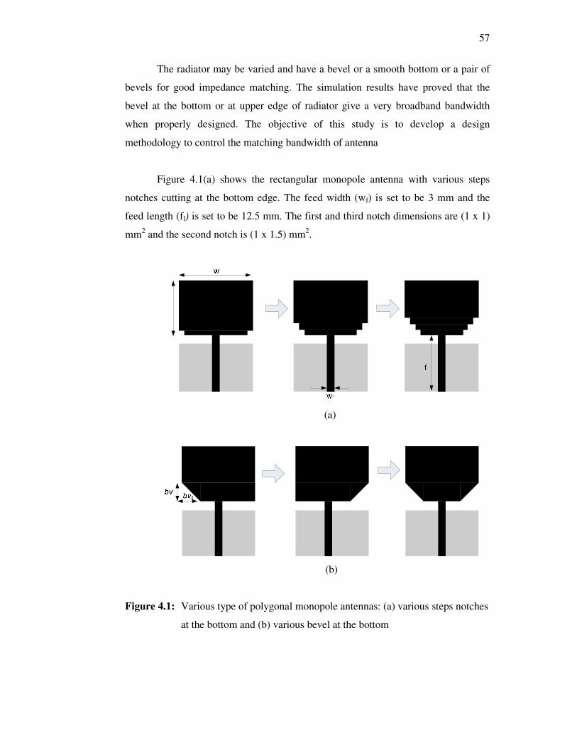
57
The radiator may be varied and have a bevel or a smooth bottom or a pair of
bevels for good impedance matching. The simulation results have proved that the
bevel at the bottom or at upper edge of radiator give a very broadband bandwidth
when properly designed. The objective of this study is to develop a design
methodology to control the matching bandwidth of antenna
Figure 4.1(a) shows the rectangular monopole antenna with various steps
notches cutting at the bottom edge. The feed width (wf) is set to be 3 mm and the
feed length (fl) is set to be 12.5 mm. The first and third notch dimensions are (1 x 1)
mm2 and the second notch is (1 x 1.5) mm
2.
(a)
(b)
Figure 4.1: Various type of polygonal monopole antennas: (a) various steps notches
at the bottom and (b) various bevel at the bottom
58
Figure 4.1(b) shows various beveling techniques applied to the rectangular
monopole antennas. Beveling at the left side, right side and both sides have shown a
different simulation results. The optimized dimension of a bevel that found to
increase the impedance bandwidth is (bv1 x bv2) of (3 mm x 2.5 mm), respectively.
The simulated return loss curves and input impedance for antenna shape in
Figure 4.1(a) are shown in Figure 4.2. Cutting notches at the bottom techniques are
aimed to change the distance between the lower part of the planar monopole antenna
and the ground plane in order to tune the capacitive coupling between the antenna
and the ground plane, thereby wider impedance bandwidth can be achieved. This
technique is confirmed by the simulation result shown in Figure 4.2. As shown in
Figure 4.2(a), the return loss of antenna with three steps notches cutting at the bottom
edge is the worst curve with respect to -10 dB. This is due to its notch variation is
more abrupt, thus the bandwidth is smaller. For the two steps notches, the return loss
curve is the best, covering 3.17 GHz to 11.5 GHz of frequency ranges. While one
step notch at the bottom provides a good matching bandwidth at below 9 GHz and
start degrading at higher frequencies.
The simulated input impedance shows the loops around matching impedance
point. It shows that the one step and three steps notches cutting at the bottom give
more capacitive to the antenna than the two steps notches especially at higher
frequency ranges. The ground plane as an impedance matching circuit and also it
tunes the resonant frequencies.
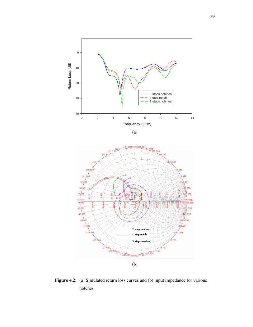
59
Frequency (GHz)
0 2 4 6 8 10 12 14
Retu
rn L
oss (
dB
)
-40
-30
-20
-10
0
3 steps notches
1 step notch
2 steps notches
(a)
(b)
Figure 4.2: (a) Simulated return loss curves and (b) input impedance for various
notches
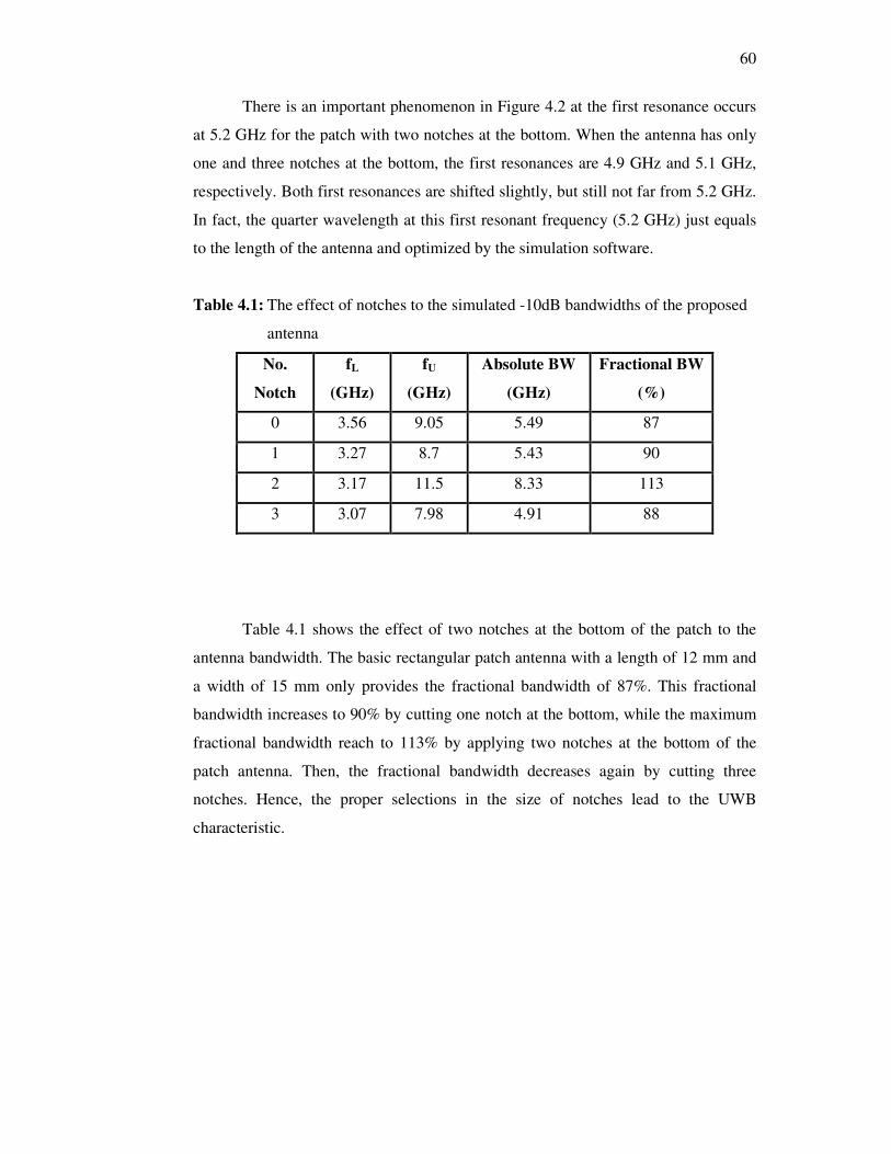
60
There is an important phenomenon in Figure 4.2 at the first resonance occurs
at 5.2 GHz for the patch with two notches at the bottom. When the antenna has only
one and three notches at the bottom, the first resonances are 4.9 GHz and 5.1 GHz,
respectively. Both first resonances are shifted slightly, but still not far from 5.2 GHz.
In fact, the quarter wavelength at this first resonant frequency (5.2 GHz) just equals
to the length of the antenna and optimized by the simulation software.
Table 4.1: The effect of notches to the simulated -10dB bandwidths of the proposed
antenna
No.
Notch
fL
(GHz)
fU
(GHz)
Absolute BW
(GHz)
Fractional BW
(%)
0 3.56 9.05 5.49 87
1 3.27 8.7 5.43 90
2 3.17 11.5 8.33 113
3 3.07 7.98 4.91 88
Table 4.1 shows the effect of two notches at the bottom of the patch to the
antenna bandwidth. The basic rectangular patch antenna with a length of 12 mm and
a width of 15 mm only provides the fractional bandwidth of 87%. This fractional
bandwidth increases to 90% by cutting one notch at the bottom, while the maximum
fractional bandwidth reach to 113% by applying two notches at the bottom of the
patch antenna. Then, the fractional bandwidth decreases again by cutting three
notches. Hence, the proper selections in the size of notches lead to the UWB
characteristic.
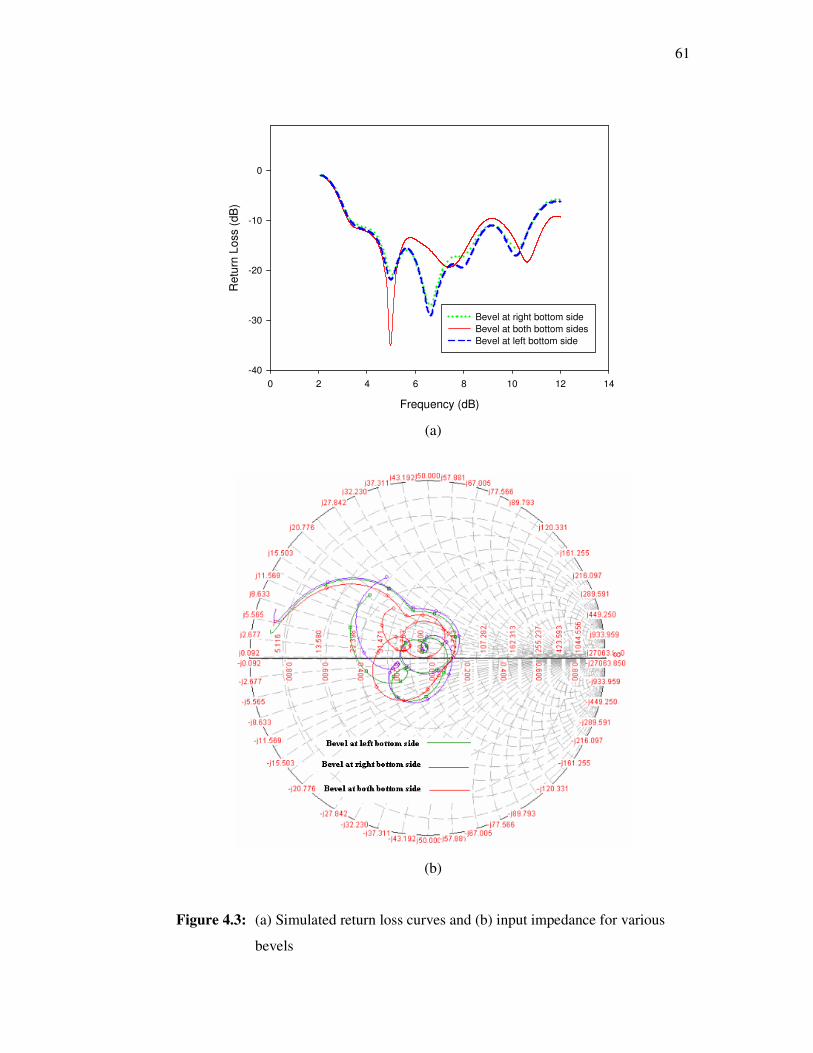
61
Frequency (dB)
0 2 4 6 8 10 12 14
Retu
rn L
oss (
dB
)
-40
-30
-20
-10
0
Bevel at right bottom side
Bevel at both bottom sides
Bevel at left bottom side
(a)
(b)
Figure 4.3: (a) Simulated return loss curves and (b) input impedance for various
bevels
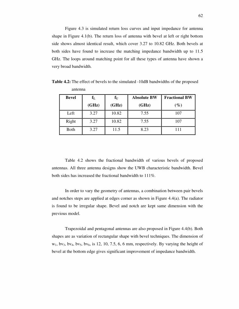
62
Figure 4.3 is simulated return loss curves and input impedance for antenna
shape in Figure 4.1(b). The return loss of antenna with bevel at left or right bottom
side shows almost identical result, which cover 3.27 to 10.82 GHz. Both bevels at
both sides have found to increase the matching impedance bandwidth up to 11.5
GHz. The loops around matching point for all these types of antenna have shown a
very broad bandwidth.
Table 4.2: The effect of bevels to the simulated -10dB bandwidths of the proposed
antenna
Bevel fL
(GHz)
fU
(GHz)
Absolute BW
(GHz)
Fractional BW
(%)
Left 3.27 10.82 7.55 107
Right 3.27 10.82 7.55 107
Both 3.27 11.5 8.23 111
Table 4.2 shows the fractional bandwidth of various bevels of proposed
antennas. All three antenna designs show the UWB characteristic bandwidth. Bevel
both sides has increased the fractional bandwidth to 111%.
In order to vary the geometry of antennas, a combination between pair bevels
and notches steps are applied at edges corner as shown in Figure 4.4(a). The radiator
is found to be irregular shape. Bevel and notch are kept same dimension with the
previous model.
Trapezoidal and pentagonal antennas are also proposed in Figure 4.4(b). Both
shapes are as variation of rectangular shape with bevel techniques. The dimension of
w1, bv3, bv4, bv5, bv6, is 12, 10, 7.5, 6, 6 mm, respectively. By varying the height of
bevel at the bottom edge gives significant improvement of impedance bandwidth.
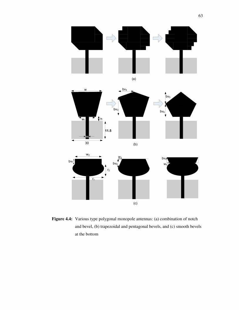
63
(a)
(b)
(c)
w1
bv4
bv3
bv5
w
wf
11.5
30
h
r1
r2
bv7
w2
bv8
w3 bv9
w4
bv6
Figure 4.4: Various type polygonal monopole antennas: (a) combination of notch
and bevel, (b) trapezoidal and pentagonal bevels, and (c) smooth bevels
at the bottom
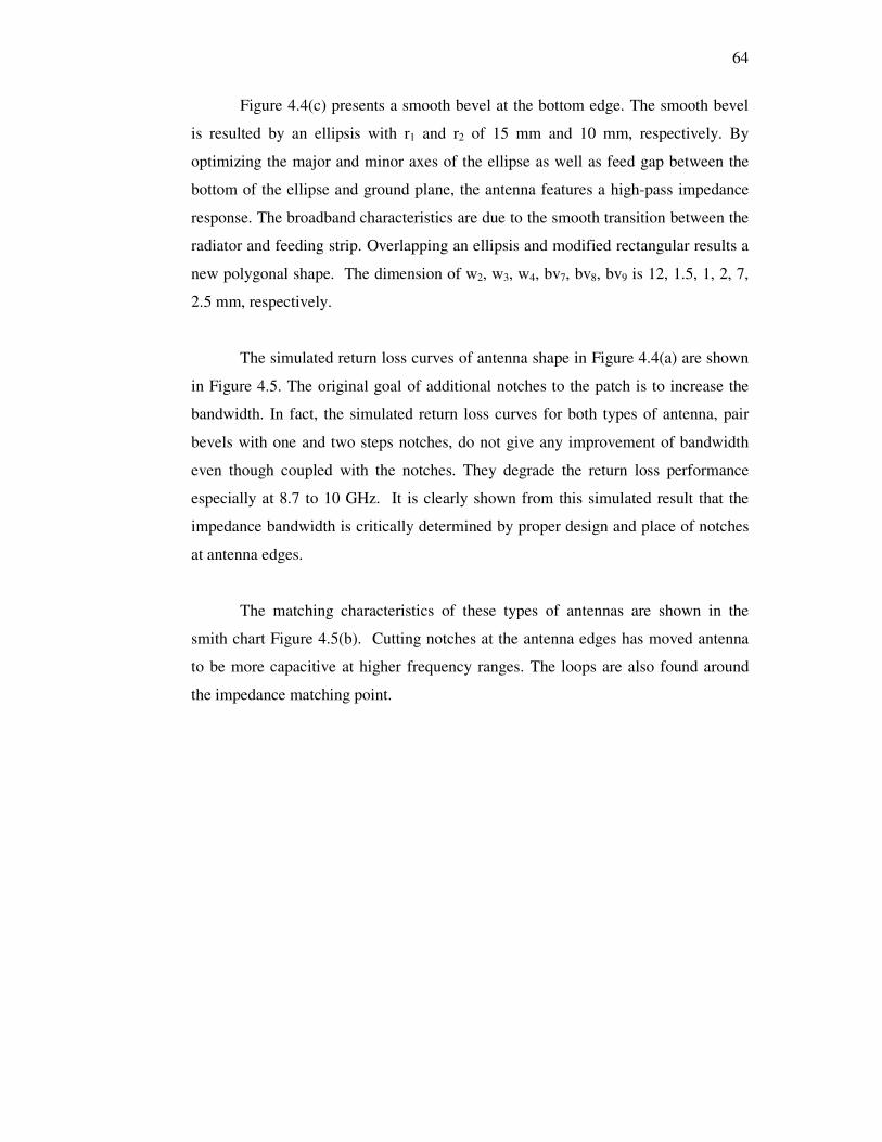
64
Figure 4.4(c) presents a smooth bevel at the bottom edge. The smooth bevel
is resulted by an ellipsis with r1 and r2 of 15 mm and 10 mm, respectively. By
optimizing the major and minor axes of the ellipse as well as feed gap between the
bottom of the ellipse and ground plane, the antenna features a high-pass impedance
response. The broadband characteristics are due to the smooth transition between the
radiator and feeding strip. Overlapping an ellipsis and modified rectangular results a
new polygonal shape. The dimension of w2, w3, w4, bv7, bv8, bv9 is 12, 1.5, 1, 2, 7,
2.5 mm, respectively.
The simulated return loss curves of antenna shape in Figure 4.4(a) are shown
in Figure 4.5. The original goal of additional notches to the patch is to increase the
bandwidth. In fact, the simulated return loss curves for both types of antenna, pair
bevels with one and two steps notches, do not give any improvement of bandwidth
even though coupled with the notches. They degrade the return loss performance
especially at 8.7 to 10 GHz. It is clearly shown from this simulated result that the
impedance bandwidth is critically determined by proper design and place of notches
at antenna edges.
The matching characteristics of these types of antennas are shown in the
smith chart Figure 4.5(b). Cutting notches at the antenna edges has moved antenna
to be more capacitive at higher frequency ranges. The loops are also found around
the impedance matching point.
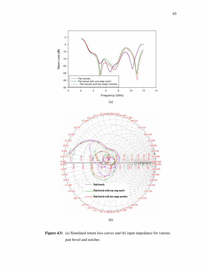
65
Frequency (GHz)
0 2 4 6 8 10 12 14
Retu
rn L
oss (dB
)
-35
-30
-25
-20
-15
-10
-5
0
Pair bevels
Pair bevel with one step notch
Pair bevels and two steps notches
(a)
(b)
Figure 4.5: (a) Simulated return loss curves and (b) input impedance for various
pair bevel and notches
66
Table 4.3: The effect of bevels coupling notches to the simulated -10dB bandwidths
of the proposed antenna
Bevel & notch fL
(GHz)
fU
(GHz)
Absolute BW
(GHz)
Fractional BW
(%)
Pair bevels 3.37 11 7.63 106
Pair bevels with
1 notch
3.37 8.56 5.19 87
Pair bevels with
2 notches
3.47 8.66 5.19 85
Table 4.3 lists the fractional bandwidth of antenna with pair bevels and notch.
An additional of notch to the antenna edge coupled with the bevels has shown the
bandwidth decrement. The maximum fractional bandwidth of 106% is achieved for
antenna with bevels at the upper and lower edges.
Trapezoidal and various height pentagonal shapes are proposed. The
simulated return loss curves and the input impedance are shown in Figure 4.6(a) and
Figure 4.6(b), respectively. The ratio between upper height and lower height are
critically determined the input impedance bandwidth. By changing the height will
degrade the return loss performance as proved in Figure 4.6(a).
The lower height determines the lower resonance frequency and the upper
height determines the upper frequency. This behavior is shown by comparing the
return loss curves between pentagonal with lower height of 10 mm and pentagonal
with lower height of 6 mm. The first type with 6 mm of height, the lower resonance
is 7 GHz while the second type is 5.2 GHz. The difference of height results much
shifted to the lower resonance frequency. The smooth beveling transition at upper
edges of pentagonal gives a flat return loss curves below -15 dB. The abrupt
transition at the upper edges has degraded the antenna performance especially at
higher frequency ranges of 8.7 to 9.7 GHz, as shown in Figure 4.6(a).
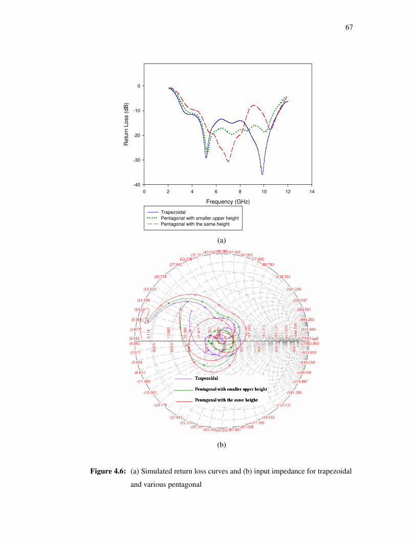
67
Frequency (GHz)
0 2 4 6 8 10 12 14
Re
turn
Lo
ss (
dB
)
-40
-30
-20
-10
0
Trapezoidal
Pentagonal with smaller upper height
Pentagonal with the same height
(a)
(b)
Figure 4.6: (a) Simulated return loss curves and (b) input impedance for trapezoidal
and various pentagonal
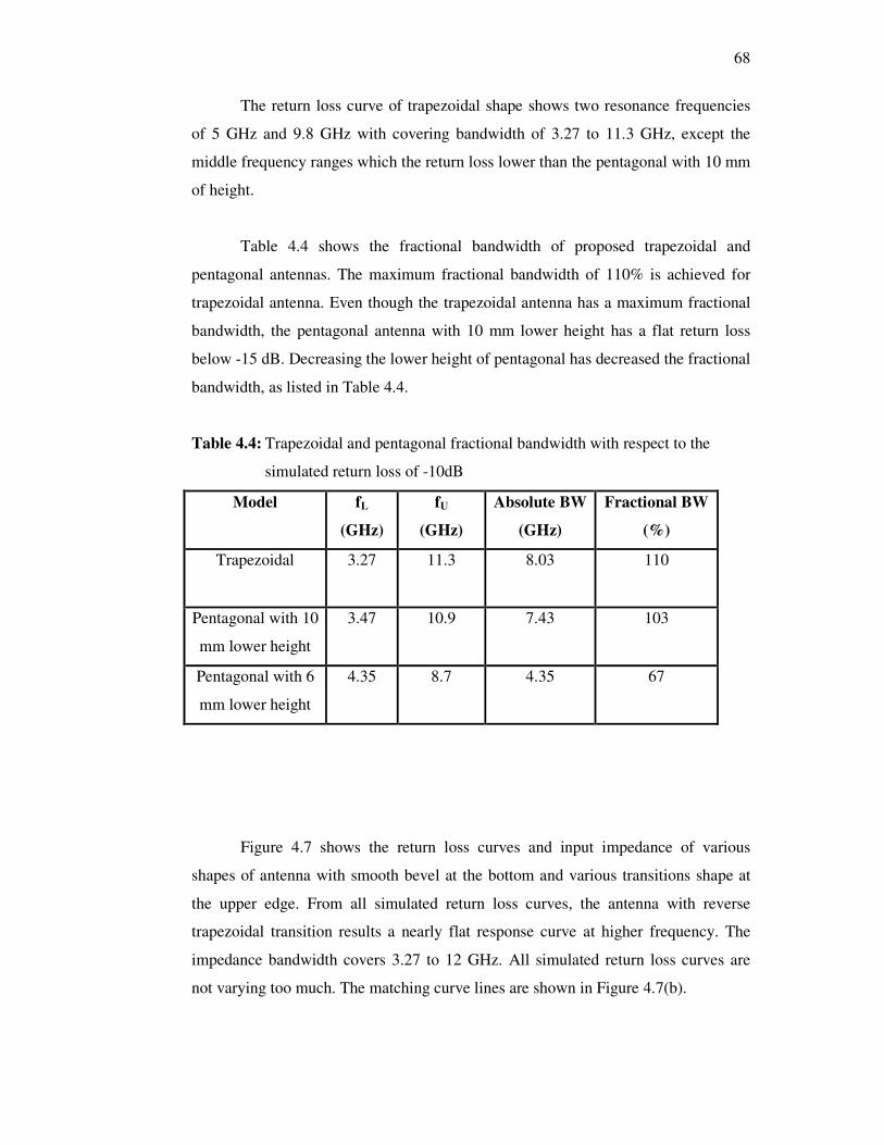
68
The return loss curve of trapezoidal shape shows two resonance frequencies
of 5 GHz and 9.8 GHz with covering bandwidth of 3.27 to 11.3 GHz, except the
middle frequency ranges which the return loss lower than the pentagonal with 10 mm
of height.
Table 4.4 shows the fractional bandwidth of proposed trapezoidal and
pentagonal antennas. The maximum fractional bandwidth of 110% is achieved for
trapezoidal antenna. Even though the trapezoidal antenna has a maximum fractional
bandwidth, the pentagonal antenna with 10 mm lower height has a flat return loss
below -15 dB. Decreasing the lower height of pentagonal has decreased the fractional
bandwidth, as listed in Table 4.4.
Table 4.4: Trapezoidal and pentagonal fractional bandwidth with respect to the
simulated return loss of -10dB
Model fL
(GHz)
fU
(GHz)
Absolute BW
(GHz)
Fractional BW
(%)
Trapezoidal 3.27 11.3 8.03 110
Pentagonal with 10
mm lower height
3.47 10.9 7.43 103
Pentagonal with 6
mm lower height
4.35 8.7 4.35 67
Figure 4.7 shows the return loss curves and input impedance of various
shapes of antenna with smooth bevel at the bottom and various transitions shape at
the upper edge. From all simulated return loss curves, the antenna with reverse
trapezoidal transition results a nearly flat response curve at higher frequency. The
impedance bandwidth covers 3.27 to 12 GHz. All simulated return loss curves are
not varying too much. The matching curve lines are shown in Figure 4.7(b).
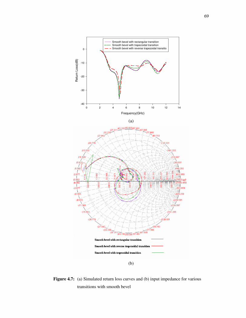
69
Frequency(GHz)
0 2 4 6 8 10 12 14
Re
turn
Lo
ss(d
B)
-40
-30
-20
-10
0
Smooth bevel with rectangular transition
Smooth bevel with trapezoidal transition
Smooth bevel with reverse trapezoidal transitio
(a)
(b)
Figure 4.7: (a) Simulated return loss curves and (b) input impedance for various
transitions with smooth bevel
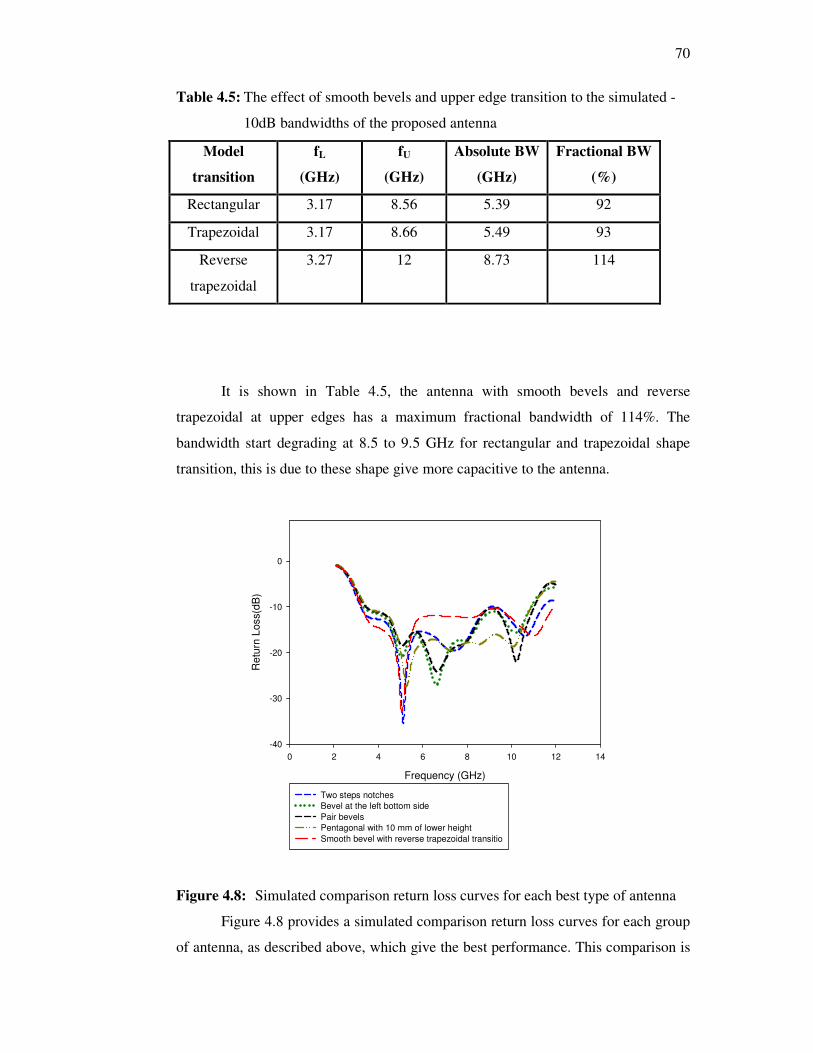
70
Table 4.5: The effect of smooth bevels and upper edge transition to the simulated -
10dB bandwidths of the proposed antenna
Model
transition
fL
(GHz)
fU
(GHz)
Absolute BW
(GHz)
Fractional BW
(%)
Rectangular 3.17 8.56 5.39 92
Trapezoidal 3.17 8.66 5.49 93
Reverse
trapezoidal
3.27 12 8.73 114
It is shown in Table 4.5, the antenna with smooth bevels and reverse
trapezoidal at upper edges has a maximum fractional bandwidth of 114%. The
bandwidth start degrading at 8.5 to 9.5 GHz for rectangular and trapezoidal shape
transition, this is due to these shape give more capacitive to the antenna.
Frequency (GHz)
0 2 4 6 8 10 12 14
Re
turn
Loss(d
B)
-40
-30
-20
-10
0
Two steps notches
Bevel at the left bottom side
Pair bevels
Pentagonal with 10 mm of lower height
Smooth bevel with reverse trapezoidal transitio
Figure 4.8: Simulated comparison return loss curves for each best type of antenna
Figure 4.8 provides a simulated comparison return loss curves for each group
of antenna, as described above, which give the best performance. This comparison is
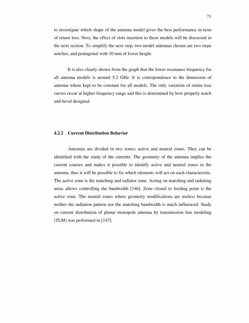
71
to investigate which shape of the antenna model gives the best performance in term
of return loss. Next, the effect of slots insertion to these models will be discussed in
the next section. To simplify the next step, two model antennas chosen are two steps
notches, and pentagonal with 10 mm of lower height.
It is also clearly shown from the graph that the lower resonance frequency for
all antenna models is around 5.2 GHz. It is correspondence to the dimension of
antenna where kept to be constant for all models. The only variation of return loss
curves occur at higher frequency range and this is determined by how properly notch
and bevel designed.
4.2.2 Current Distribution Behavior
Antennas are divided in two zones; active and neutral zones. They can be
identified with the study of the currents. The geometry of the antenna implies the
current courses and makes it possible to identify active and neutral zones in the
antenna, thus it will be possible to fix which elements will act on each characteristic.
The active zone is the matching and radiator zone. Acting on matching and radiating
areas allows controlling the bandwidth [146]. Zone closed to feeding point is the
active zone. The neutral zones where geometry modifications are useless because
neither the radiation pattern nor the matching bandwidth is much influenced. Study
on current distribution of planar monopole antenna by transmission line modeling
(TLM) was performed in [147].
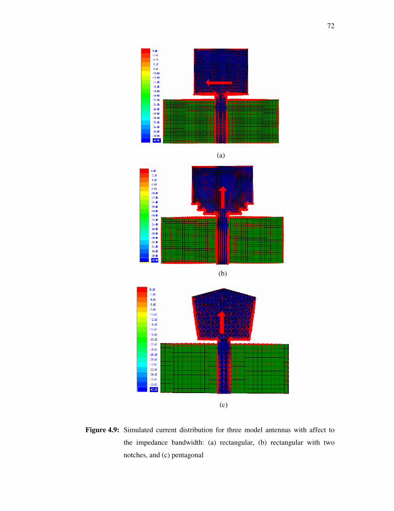
72
(a)
(b)
(c)
Figure 4.9: Simulated current distribution for three model antennas with affect to
the impedance bandwidth: (a) rectangular, (b) rectangular with two
notches, and (c) pentagonal
73
Matching bandwidth is due to the shape of the antenna closed to the feeding
point, where currents are the strongest. It is possible to enlarge or reduce it in
accordance with the application to implement by modifying its geometry close to this
one as shown in Figure 4.9. Figure shows the current distribution for three model
antennas at 7.5 GHz, such as rectangular, pentagonal with 10 mm of lower height
and rectangular with two notches. As mentioned in Chapter 3, when properly
designed, the bevels and notches improve significantly the impedance bandwidth at
upper frequency.
The study of the current flow on a planar monopole antenna reveals that it is
mostly concentrated in the vertical and horizontal edges, as shown in Figure 4.9. It is
observed that the horizontal currents distributions are focused on the bottom edge of
rectangular patch. Besides, the horizontal component is also greater than the vertical
on this part of the antenna. The field supported by these currents would be mainly
confined between the bottom part of the rectangular antenna and the ground plane;
this is due to the small distance, a small fraction of wavelength, of this edge to the
ground plane [147]. Thereby, this part acts as a matching element.
Figure 4.10 shows the return loss performance of this rectangular antenna.
The return loss starts degrading its performance at 7.5 GHz, this is due to more
horizontal current mode occurs in the whole structure which degrade the polarization
properties and the impedance bandwidth performance of the antenna [129]. In order
to modify the equivalent characteristic impedance on the antenna, the distance of the
bottom edge to the ground plane and the bottom profile of the monopole should be
varied. By varying the edges closed to the feeding point means modifying the current
path on the antenna.
The discontinuity occurred from cutting notch or beveling at the bottom side
of a rectangular antenna has enforced the excitation of a particular characteristic
mode (the vertical current mode) in the structure, which presents a very wide
bandwidth. Much current density occurs closed to the feeding edge, while at the top
of antenna; the current levels are not too strong as shown by simulated result in
Figure 4.9(b) and Figure 4.9(c). From the simulated return loss, the rectangular shape
has the smallest impedance bandwidth. In addition, the double notches at the base of
74
the antenna have demonstrated to shift upward the upper edge frequency of the
bandwidth.
Frequency(GHz)
0 2 4 6 8 10 12 14
Re
turn
Lo
ss
(dB
)
-40
-30
-20
-10
0
Rectangular
Two notches
Pentagonal
Figure 4.10: Simulated return loss for three model antennas with affect to the
impedance bandwidth
To better control an antenna behavior, it is necessary to identify neutral
zones. The neutral zone can be used to simplify the antenna structure and integrate
other function of the systems such as antenna circuits. This investigation has been
proposed in [146], but not much explanation given. How to determine the neutral
zone is not explained in detail.
Thorough literature reviews [146]-[147] and simulation experiences, there are
four types of current distribution modes in the antenna surface; vertical current mode,
horizontal current mode, diagonal current mode and asymmetry current mode. By
observing the current distribution flow, the pentagonal has a diamond neutral zone
and both rectangular and two steps notches have a rectangular neutral zone. In this
zone, the current level is not too strong but it is not zero level. Normally, this zone
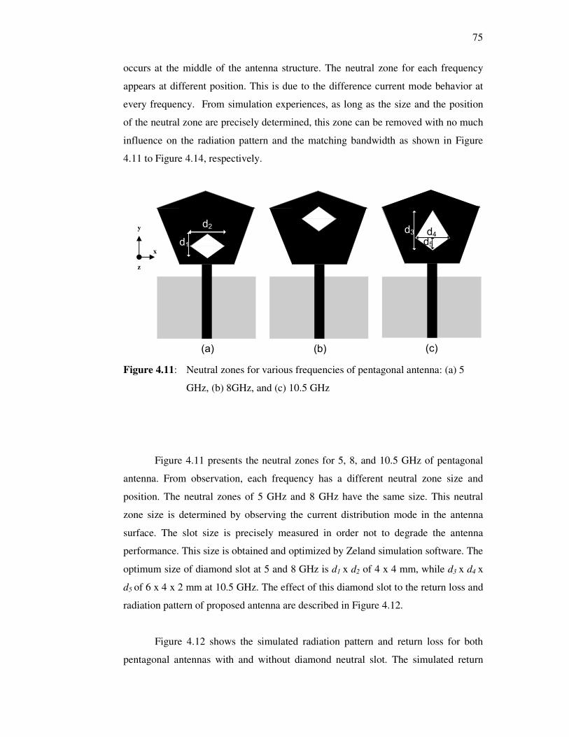
75
occurs at the middle of the antenna structure. The neutral zone for each frequency
appears at different position. This is due to the difference current mode behavior at
every frequency. From simulation experiences, as long as the size and the position
of the neutral zone are precisely determined, this zone can be removed with no much
influence on the radiation pattern and the matching bandwidth as shown in Figure
4.11 to Figure 4.14, respectively.
d2
d1
(c)
d3 d4d5
(b)(a)
Figure 4.11: Neutral zones for various frequencies of pentagonal antenna: (a) 5
GHz, (b) 8GHz, and (c) 10.5 GHz
Figure 4.11 presents the neutral zones for 5, 8, and 10.5 GHz of pentagonal
antenna. From observation, each frequency has a different neutral zone size and
position. The neutral zones of 5 GHz and 8 GHz have the same size. This neutral
zone size is determined by observing the current distribution mode in the antenna
surface. The slot size is precisely measured in order not to degrade the antenna
performance. This size is obtained and optimized by Zeland simulation software. The
optimum size of diamond slot at 5 and 8 GHz is d1 x d2 of 4 x 4 mm, while d3 x d4 x
d5 of 6 x 4 x 2 mm at 10.5 GHz. The effect of this diamond slot to the return loss and
radiation pattern of proposed antenna are described in Figure 4.12.
Figure 4.12 shows the simulated radiation pattern and return loss for both
pentagonal antennas with and without diamond neutral slot. The simulated return
y
x
z
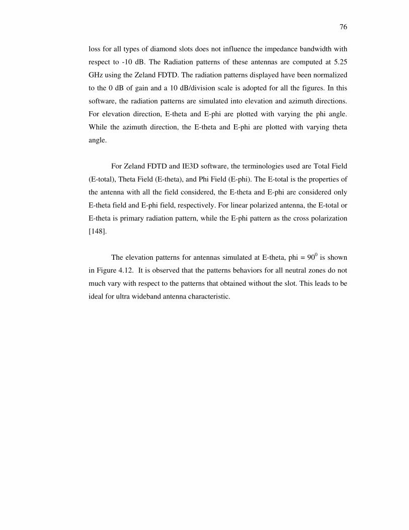
76
loss for all types of diamond slots does not influence the impedance bandwidth with
respect to -10 dB. The Radiation patterns of these antennas are computed at 5.25
GHz using the Zeland FDTD. The radiation patterns displayed have been normalized
to the 0 dB of gain and a 10 dB/division scale is adopted for all the figures. In this
software, the radiation patterns are simulated into elevation and azimuth directions.
For elevation direction, E-theta and E-phi are plotted with varying the phi angle.
While the azimuth direction, the E-theta and E-phi are plotted with varying theta
angle.
For Zeland FDTD and IE3D software, the terminologies used are Total Field
(E-total), Theta Field (E-theta), and Phi Field (E-phi). The E-total is the properties of
the antenna with all the field considered, the E-theta and E-phi are considered only
E-theta field and E-phi field, respectively. For linear polarized antenna, the E-total or
E-theta is primary radiation pattern, while the E-phi pattern as the cross polarization
[148].
The elevation patterns for antennas simulated at E-theta, phi = 900 is shown
in Figure 4.12. It is observed that the patterns behaviors for all neutral zones do not
much vary with respect to the patterns that obtained without the slot. This leads to be
ideal for ultra wideband antenna characteristic.
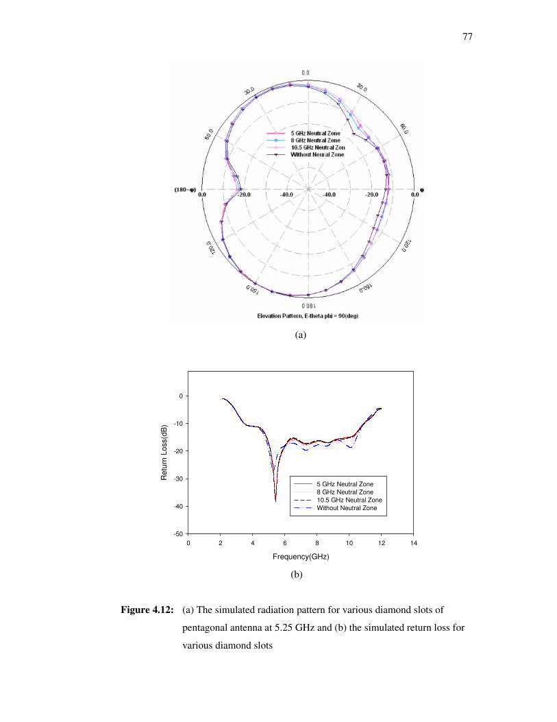
77
(a)
Frequency(GHz)
0 2 4 6 8 10 12 14
Re
turn
Lo
ss(d
B)
-50
-40
-30
-20
-10
0
5 GHz Neutral Zone
8 GHz Neutral Zone
10.5 GHz Neutral Zone
Without Neutral Zone
(b)
Figure 4.12: (a) The simulated radiation pattern for various diamond slots of
pentagonal antenna at 5.25 GHz and (b) the simulated return loss for
various diamond slots
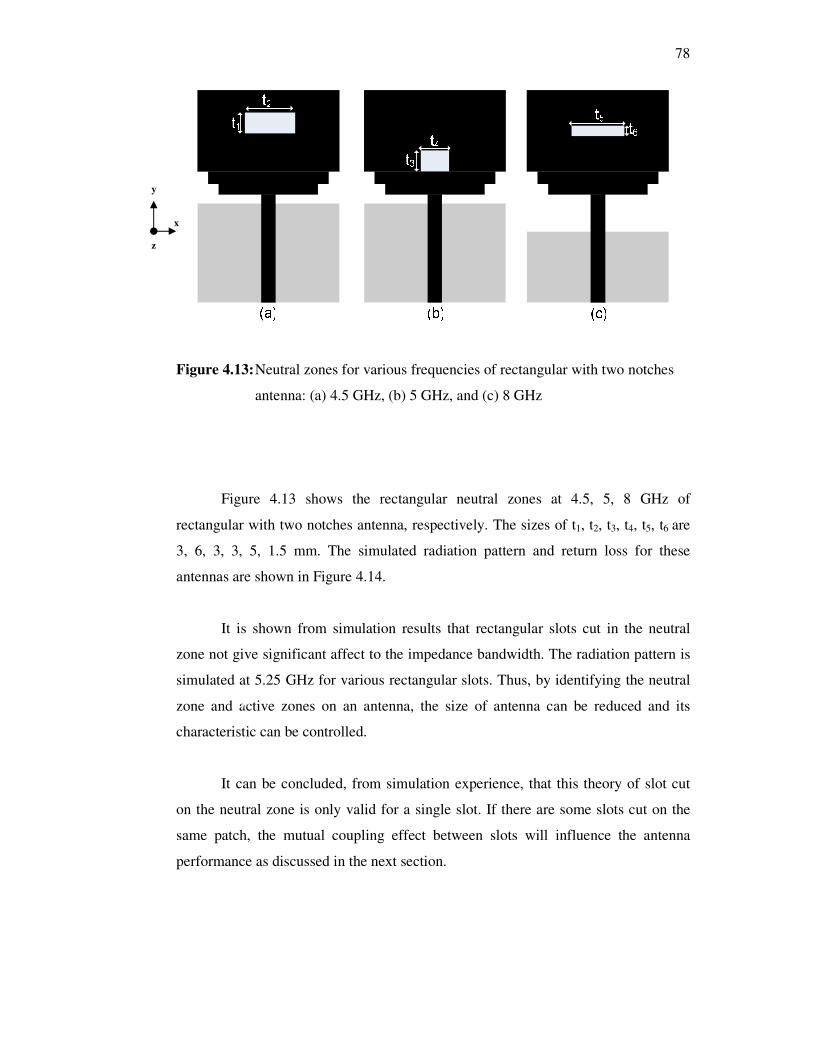
78
Figure 4.13: Neutral zones for various frequencies of rectangular with two notches
antenna: (a) 4.5 GHz, (b) 5 GHz, and (c) 8 GHz
Figure 4.13 shows the rectangular neutral zones at 4.5, 5, 8 GHz of
rectangular with two notches antenna, respectively. The sizes of t1, t2, t3, t4, t5, t6 are
3, 6, 3, 3, 5, 1.5 mm. The simulated radiation pattern and return loss for these
antennas are shown in Figure 4.14.
It is shown from simulation results that rectangular slots cut in the neutral
zone not give significant affect to the impedance bandwidth. The radiation pattern is
simulated at 5.25 GHz for various rectangular slots. Thus, by identifying the neutral
zone and active zones on an antenna, the size of antenna can be reduced and its
characteristic can be controlled.
It can be concluded, from simulation experience, that this theory of slot cut
on the neutral zone is only valid for a single slot. If there are some slots cut on the
same patch, the mutual coupling effect between slots will influence the antenna
performance as discussed in the next section.
y
x
z
t1
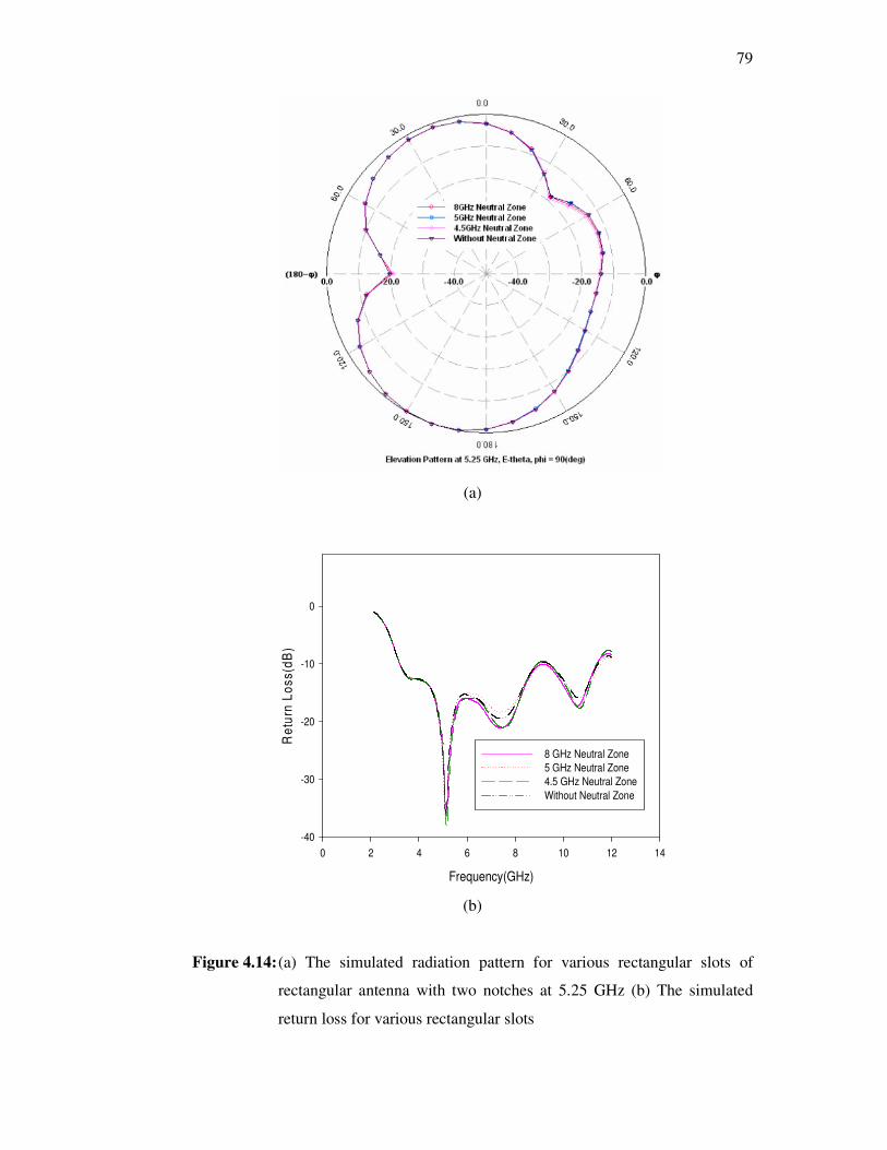
79
(a)
Frequency(GHz)
0 2 4 6 8 10 12 14
Re
turn
Lo
ss
(dB
)
-40
-30
-20
-10
0
8 GHz Neutral Zone
5 GHz Neutral Zone
4.5 GHz Neutral Zone
Without Neutral Zone
(b)
Figure 4.14: (a) The simulated radiation pattern for various rectangular slots of
rectangular antenna with two notches at 5.25 GHz (b) The simulated
return loss for various rectangular slots
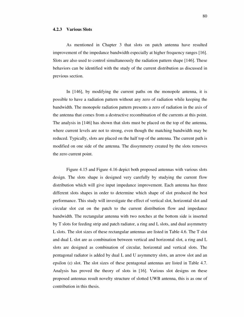
80
4.2.3 Various Slots
As mentioned in Chapter 3 that slots on patch antenna have resulted
improvement of the impedance bandwidth especially at higher frequency ranges [16].
Slots are also used to control simultaneously the radiation pattern shape [146]. These
behaviors can be identified with the study of the current distribution as discussed in
previous section.
In [146], by modifying the current paths on the monopole antenna, it is
possible to have a radiation pattern without any zero of radiation while keeping the
bandwidth. The monopole radiation pattern presents a zero of radiation in the axis of
the antenna that comes from a destructive recombination of the currents at this point.
The analysis in [146] has shown that slots must be placed on the top of the antenna,
where current levels are not to strong, even though the matching bandwidth may be
reduced. Typically, slots are placed on the half top of the antenna. The current path is
modified on one side of the antenna. The dissymmetry created by the slots removes
the zero current point.
Figure 4.15 and Figure 4.16 depict both proposed antennas with various slots
design. The slots shape is designed very carefully by studying the current flow
distribution which will give input impedance improvement. Each antenna has three
different slots shapes in order to determine which shape of slot produced the best
performance. This study will investigate the effect of vertical slot, horizontal slot and
circular slot cut on the patch to the current distribution flow and impedance
bandwidth. The rectangular antenna with two notches at the bottom side is inserted
by T slots for feeding strip and patch radiator, a ring and L slots, and dual asymmetry
L slots. The slot sizes of these rectangular antennas are listed in Table 4.6. The T slot
and dual L slot are as combination between vertical and horizontal slot, a ring and L
slots are designed as combination of circular, horizontal and vertical slots. The
pentagonal radiator is added by dual L and U asymmetry slots, an arrow slot and an
epsilon (ε) slot. The slot sizes of these pentagonal antennas are listed in Table 4.7.
Analysis has proved the theory of slots in [16]. Various slot designs on these
proposed antennas result novelty structure of slotted UWB antenna, this is as one of
contribution in this thesis.
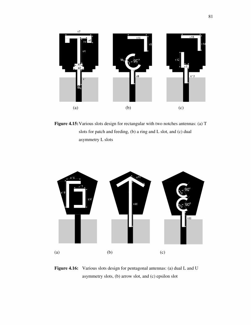
81
(a) (b) (c)
Figure 4.15: Various slots design for rectangular with two notches antennas: (a) T
slots for patch and feeding, (b) a ring and L slot, and (c) dual
asymmetry L slots
(a) (b) (c)
Figure 4.16: Various slots design for pentagonal antennas: (a) dual L and U
asymmetry slots, (b) arrow slot, and (c) epsilon slot
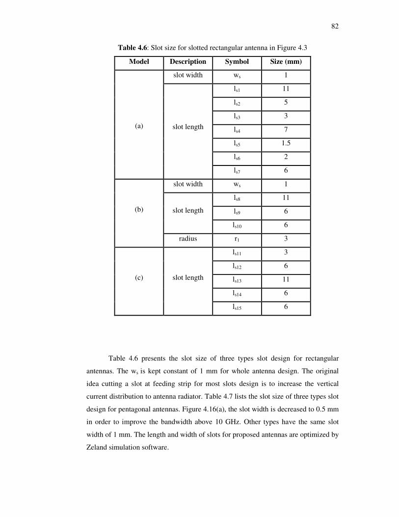
82
Table 4.6: Slot size for slotted rectangular antenna in Figure 4.3
Model Description Symbol Size (mm)
slot width ws 1
ls1 11
ls2 5
ls3 3
ls4 7
ls5 1.5
ls6 2
(a)
slot length
ls7 6
slot width ws 1
ls8 11
ls9 6
slot length
ls10 6
(b)
radius r1 3
ls11 3
ls12 6
ls13 11
ls14 6
(c)
slot length
ls15 6
Table 4.6 presents the slot size of three types slot design for rectangular
antennas. The ws is kept constant of 1 mm for whole antenna design. The original
idea cutting a slot at feeding strip for most slots design is to increase the vertical
current distribution to antenna radiator. Table 4.7 lists the slot size of three types slot
design for pentagonal antennas. Figure 4.16(a), the slot width is decreased to 0.5 mm
in order to improve the bandwidth above 10 GHz. Other types have the same slot
width of 1 mm. The length and width of slots for proposed antennas are optimized by
Zeland simulation software.
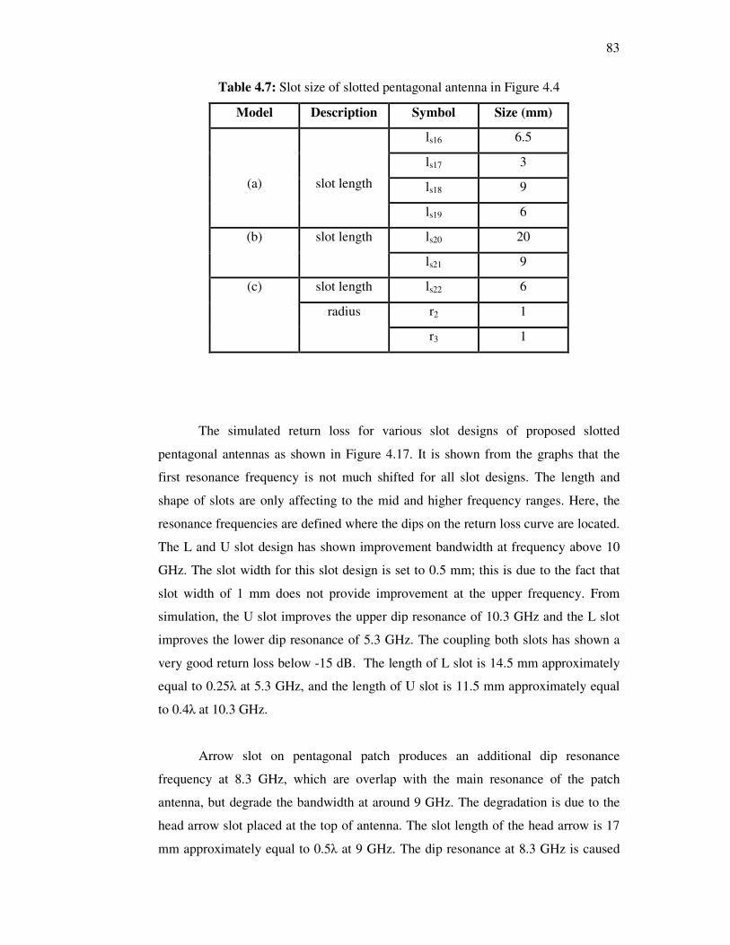
83
Table 4.7: Slot size of slotted pentagonal antenna in Figure 4.4
Model Description Symbol Size (mm)
ls16 6.5
ls17 3
ls18 9
(a)
slot length
ls19 6
ls20 20 (b) slot length
ls21 9
slot length ls22 6
r2 1
(c)
radius
r3 1
The simulated return loss for various slot designs of proposed slotted
pentagonal antennas as shown in Figure 4.17. It is shown from the graphs that the
first resonance frequency is not much shifted for all slot designs. The length and
shape of slots are only affecting to the mid and higher frequency ranges. Here, the
resonance frequencies are defined where the dips on the return loss curve are located.
The L and U slot design has shown improvement bandwidth at frequency above 10
GHz. The slot width for this slot design is set to 0.5 mm; this is due to the fact that
slot width of 1 mm does not provide improvement at the upper frequency. From
simulation, the U slot improves the upper dip resonance of 10.3 GHz and the L slot
improves the lower dip resonance of 5.3 GHz. The coupling both slots has shown a
very good return loss below -15 dB. The length of L slot is 14.5 mm approximately
equal to 0.25λ at 5.3 GHz, and the length of U slot is 11.5 mm approximately equal
to 0.4λ at 10.3 GHz.
Arrow slot on pentagonal patch produces an additional dip resonance
frequency at 8.3 GHz, which are overlap with the main resonance of the patch
antenna, but degrade the bandwidth at around 9 GHz. The degradation is due to the
head arrow slot placed at the top of antenna. The slot length of the head arrow is 17
mm approximately equal to 0.5λ at 9 GHz. The dip resonance at 8.3 GHz is caused
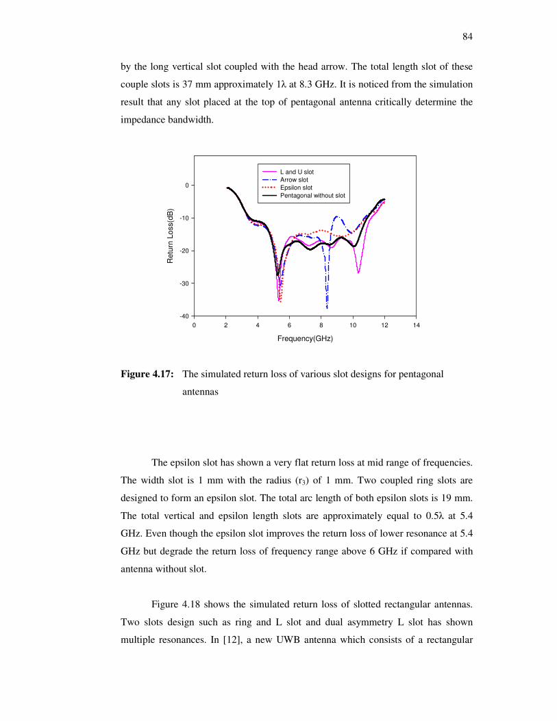
84
by the long vertical slot coupled with the head arrow. The total length slot of these
couple slots is 37 mm approximately 1λ at 8.3 GHz. It is noticed from the simulation
result that any slot placed at the top of pentagonal antenna critically determine the
impedance bandwidth.
Frequency(GHz)
0 2 4 6 8 10 12 14
Retu
rn L
oss(d
B)
-40
-30
-20
-10
0
L and U slot
Arrow slot
Epsilon slot
Pentagonal without slot
Figure 4.17: The simulated return loss of various slot designs for pentagonal
antennas
The epsilon slot has shown a very flat return loss at mid range of frequencies.
The width slot is 1 mm with the radius (r3) of 1 mm. Two coupled ring slots are
designed to form an epsilon slot. The total arc length of both epsilon slots is 19 mm.
The total vertical and epsilon length slots are approximately equal to 0.5λ at 5.4
GHz. Even though the epsilon slot improves the return loss of lower resonance at 5.4
GHz but degrade the return loss of frequency range above 6 GHz if compared with
antenna without slot.
Figure 4.18 shows the simulated return loss of slotted rectangular antennas.
Two slots design such as ring and L slot and dual asymmetry L slot has shown
multiple resonances. In [12], a new UWB antenna which consists of a rectangular
85
patch with two steps, a single slot on the patch, and a partial ground plane is
reported. However, the performance and characteristic of this antenna is not analyzed
in detail. How exactly this antenna operates across the entire bandwidth, remains a
question. With this proposed various slot on rectangular antenna with two steps, the
effect of slot to the antenna performances are investigated in detail.
Frequency(dB)
0 2 4 6 8 10 12 14
Retu
rn L
oss(d
B)
-50
-40
-30
-20
-10
0
T slot
Ring and L slots
Dual asymmetry L slots
Rectangular with two notches without slot
Figure 4.18: The simulated return loss of various slot designs for rectangular with
two notches antennas
The T slot on the feeding strip produces more vertical current thus improve
the matching impedance performance at higher frequencies. The length of the T slot
on the feeding strip is designed approximately equal to 2
λ at 10.5 GHz. From the
graph in Figure 4.18, at upper frequency of 10.5 GHz of T slotted antenna, the S11
reaches -30 dB. The bandwidth enhancement is due to much more vertical electrical
current achieved in the patch through the T slots resulting in much regular
distribution of the magnetic current in the slots. While the T slot cut on the patch
shows the return loss improvement at the first resonant point of 5.2 GHz. By cutting
the slots on the patch disturb the current distribution flow. Thus, the slot wideband
86
behavior is due to the fact that the currents along the edges of the slot introduce the
same resonance frequencies, which, in conjunction with the resonance of the main
patch, produce an overall broadband frequency response characteristic. The slot also
appears to introduce a capacitive reactance which counteracts the inductive reactance
of the feed [109]-[110]. Thus, the bandwidth broadening comes from the patch and
T-slot, coupled together to form UWB characteristic [111]. The use of slot embedded
on the microstrip patch has been investigated extensively in [109], [111][149]-[151].
This most successful technique utilizes a coupled resonator approach, in which the
microstrip patch acts as one of the resonator and slot as the second resonator near its
resonance [149].
The ring slot with the open angle of 90o and radius (r1) of 3 mm has shown an
improvement to the return loss at the lower resonance of 5 GHz and the upper
resonance of 10 GHz. The arc length of ring slot is 19 mm. The total length of
vertical slot and ring slot is approximately equal to 1λ at 10 GHz. The vertical slot
cutting at the feeding strip has guided the vertical electrical current flowing through
the antenna radiator and most concentrated near to the ring edge. The L slot at the
right upper corner of the patch shows the second dip resonance at 7.3 GHz. The
length of L slot is 11 mm and optimized by the Zeland simulation software. This
coupled slot has presented multiple resonances which cover 3 to 12 GHz frequency
range.
The dual asymmetry L slot on rectangular patch has shown multiple
resonances. The second dip resonance of 7.1 GHz is due to the right upper corner L
slot length, while the dip resonance of 10.7 GHz is caused by the lower L slot. The
lengths of right upper L slot and the lower L slot are 11 mm and 9 mm and
approximately equal to 0.25λ at 7.1 GHz and 0.3λ at 10.7 GHz, respectively. Both
coupled asymmetry L slots has provided the UWB characteristic which cover 3.1 to
11.7 GHz.
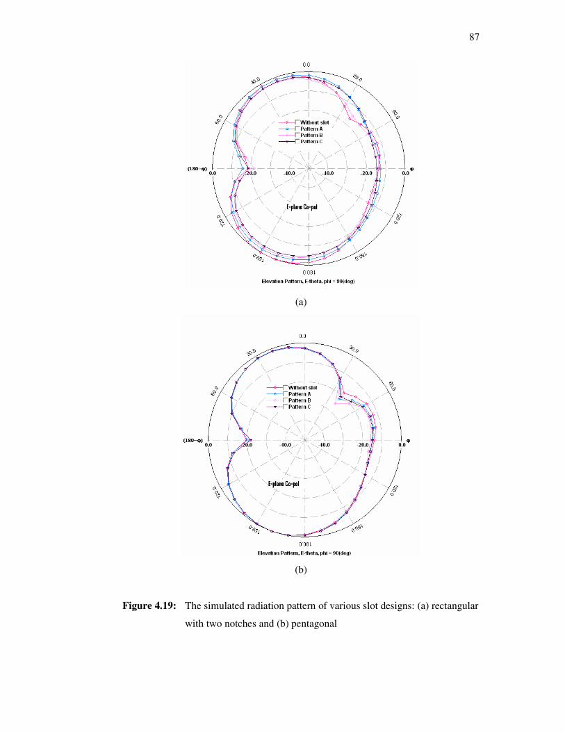
87
(a)
(b)
Figure 4.19: The simulated radiation pattern of various slot designs: (a) rectangular
with two notches and (b) pentagonal
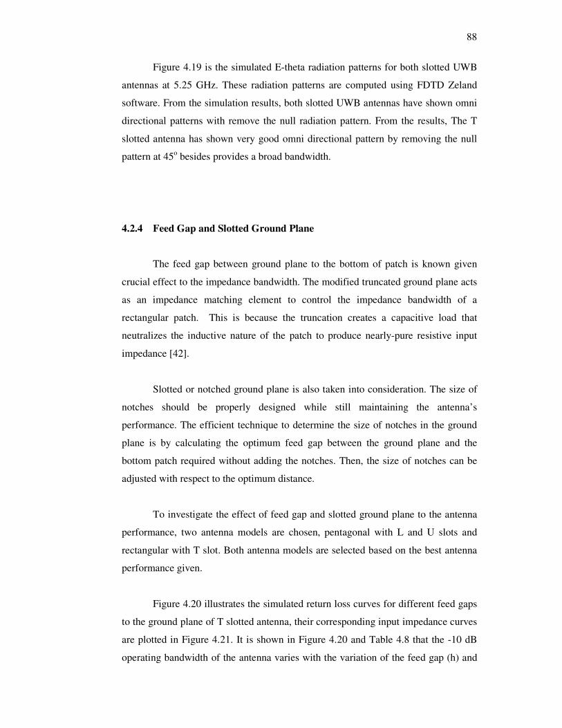
88
Figure 4.19 is the simulated E-theta radiation patterns for both slotted UWB
antennas at 5.25 GHz. These radiation patterns are computed using FDTD Zeland
software. From the simulation results, both slotted UWB antennas have shown omni
directional patterns with remove the null radiation pattern. From the results, The T
slotted antenna has shown very good omni directional pattern by removing the null
pattern at 45o besides provides a broad bandwidth.
4.2.4 Feed Gap and Slotted Ground Plane
The feed gap between ground plane to the bottom of patch is known given
crucial effect to the impedance bandwidth. The modified truncated ground plane acts
as an impedance matching element to control the impedance bandwidth of a
rectangular patch. This is because the truncation creates a capacitive load that
neutralizes the inductive nature of the patch to produce nearly-pure resistive input
impedance [42].
Slotted or notched ground plane is also taken into consideration. The size of
notches should be properly designed while still maintaining the antenna’s
performance. The efficient technique to determine the size of notches in the ground
plane is by calculating the optimum feed gap between the ground plane and the
bottom patch required without adding the notches. Then, the size of notches can be
adjusted with respect to the optimum distance.
To investigate the effect of feed gap and slotted ground plane to the antenna
performance, two antenna models are chosen, pentagonal with L and U slots and
rectangular with T slot. Both antenna models are selected based on the best antenna
performance given.
Figure 4.20 illustrates the simulated return loss curves for different feed gaps
to the ground plane of T slotted antenna, their corresponding input impedance curves
are plotted in Figure 4.21. It is shown in Figure 4.20 and Table 4.8 that the -10 dB
operating bandwidth of the antenna varies with the variation of the feed gap (h) and
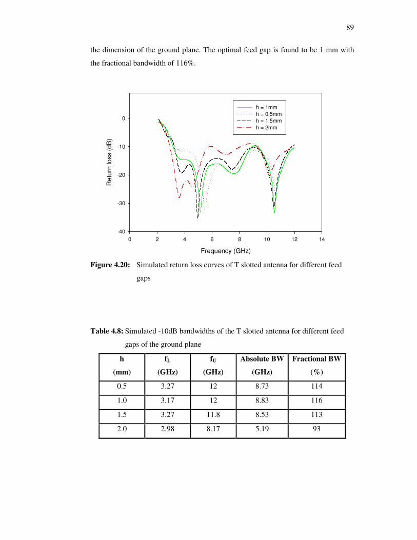
89
the dimension of the ground plane. The optimal feed gap is found to be 1 mm with
the fractional bandwidth of 116%.
Frequency (GHz)
0 2 4 6 8 10 12 14
Retu
rn lo
ss (
dB
)
-40
-30
-20
-10
0
h = 1mm
h = 0.5mm
h = 1.5mm
h = 2mm
Figure 4.20: Simulated return loss curves of T slotted antenna for different feed
gaps
Table 4.8: Simulated -10dB bandwidths of the T slotted antenna for different feed
gaps of the ground plane
h
(mm)
fL
(GHz)
fU
(GHz)
Absolute BW
(GHz)
Fractional BW
(%)
0.5 3.27 12 8.73 114
1.0 3.17 12 8.83 116
1.5 3.27 11.8 8.53 113
2.0 2.98 8.17 5.19 93
90
It can be seen in Table 4.8 that the -10 dB bandwidth of T slotted antenna
does not change much with the variation of the feed gap of the ground plane below
1.5 mm. But beyond this ranges, it will degrade the impedance bandwidth
performance. These simulated results indicate that the antenna bandwidth is
dependent on the feed gap of the ground plane, since the ground plane serves as an
impedance matching circuit.
As shown in Figure 4.21(a), the return loss < -10 dB always occurs over the
frequency range when the input impedance is matched to 50 ohm. The real part (Re)
is close to 50 Ω while the imaginary part (Im), as shown in Figure 4.21(b), is not far
from zero for the four different feed gaps. When h is 1mm and 1.5 mm, Re varies
tardily at the level of 50 Ω whilst Im remains small across wide frequency range,
leading to a UWB characteristic. However, when h rises to 2 mm, Re varies more
widely and Im also fluctuates significantly across the frequency range, thus resulting
in impedance mismatch at the antenna and hence the decrease of the operating
bandwidth. The peak value of resistance is as high as 100 ohms, while the maximum
reactance is around 35 ohms.
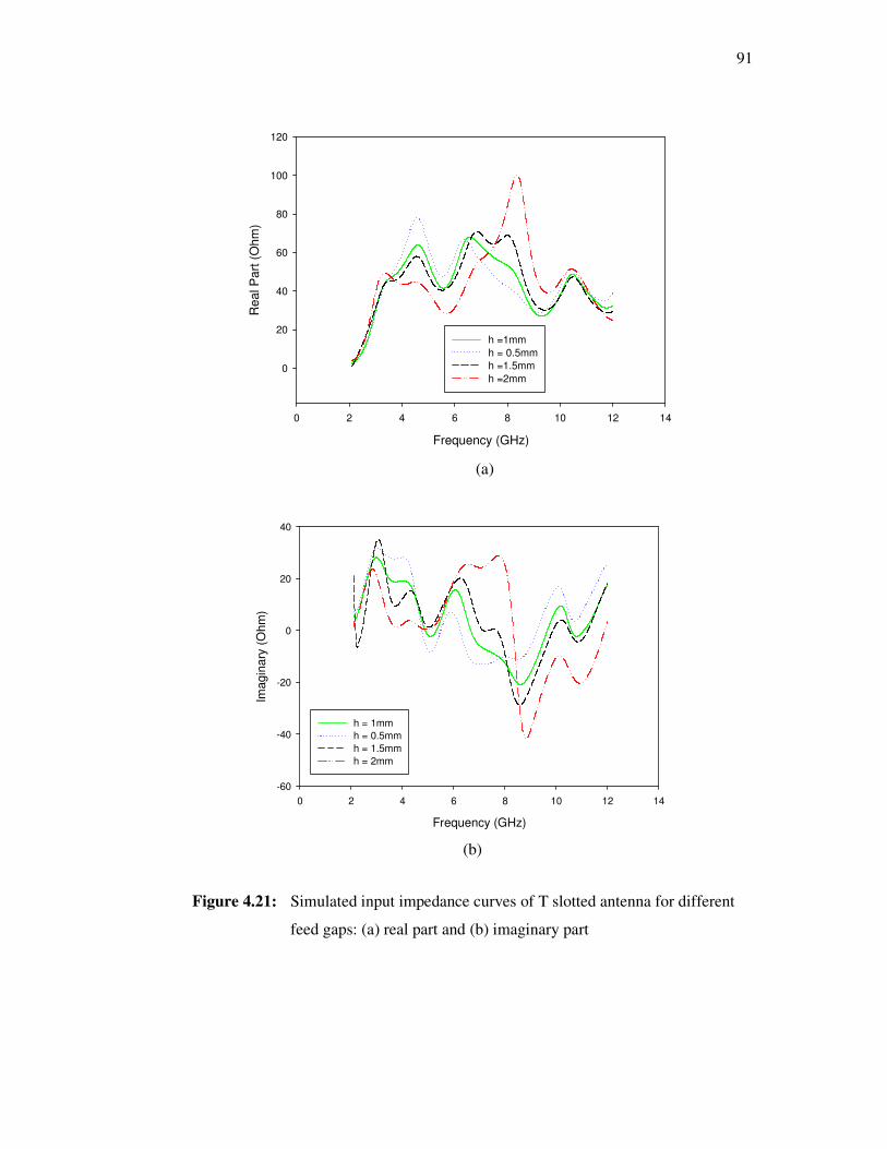
91
Frequency (GHz)
0 2 4 6 8 10 12 14
Real P
art
(O
hm
)
0
20
40
60
80
100
120
h =1mm
h = 0.5mm
h =1.5mm
h =2mm
(a)
Frequency (GHz)
0 2 4 6 8 10 12 14
Ima
gin
ary
(O
hm
)
-60
-40
-20
0
20
40
h = 1mm
h = 0.5mm
h = 1.5mm
h = 2mm
(b)
Figure 4.21: Simulated input impedance curves of T slotted antenna for different
feed gaps: (a) real part and (b) imaginary part
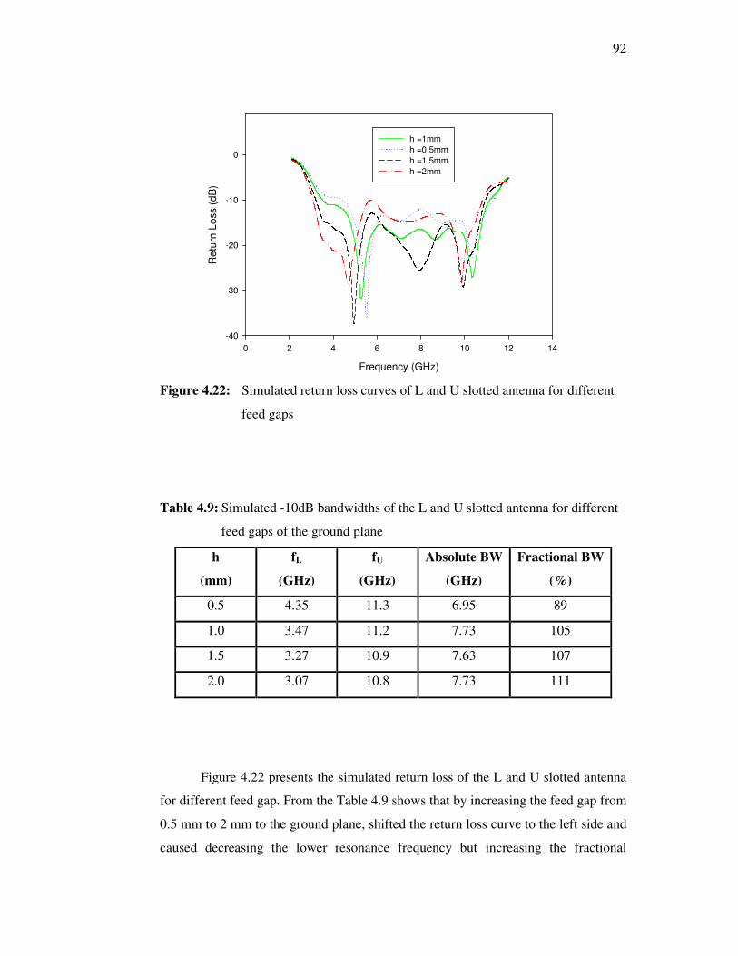
92
Frequency (GHz)
0 2 4 6 8 10 12 14
Retu
rn L
oss (
dB
)
-40
-30
-20
-10
0
h =1mm
h =0.5mm
h =1.5mm
h =2mm
Figure 4.22: Simulated return loss curves of L and U slotted antenna for different
feed gaps
Table 4.9: Simulated -10dB bandwidths of the L and U slotted antenna for different
feed gaps of the ground plane
h
(mm)
fL
(GHz)
fU
(GHz)
Absolute BW
(GHz)
Fractional BW
(%)
0.5 4.35 11.3 6.95 89
1.0 3.47 11.2 7.73 105
1.5 3.27 10.9 7.63 107
2.0 3.07 10.8 7.73 111
Figure 4.22 presents the simulated return loss of the L and U slotted antenna
for different feed gap. From the Table 4.9 shows that by increasing the feed gap from
0.5 mm to 2 mm to the ground plane, shifted the return loss curve to the left side and
caused decreasing the lower resonance frequency but increasing the fractional
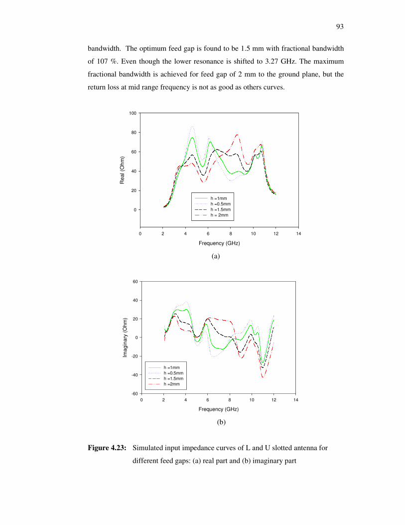
93
bandwidth. The optimum feed gap is found to be 1.5 mm with fractional bandwidth
of 107 %. Even though the lower resonance is shifted to 3.27 GHz. The maximum
fractional bandwidth is achieved for feed gap of 2 mm to the ground plane, but the
return loss at mid range frequency is not as good as others curves.
Frequency (GHz)
0 2 4 6 8 10 12 14
Re
al (O
hm
)
0
20
40
60
80
100
h =1mm
h =0.5mm
h =1.5mm
h = 2mm
(a)
Frequency (GHz)
0 2 4 6 8 10 12 14
Ima
gin
ary
(O
hm
)
-60
-40
-20
0
20
40
60
h =1mm
h =0.5mm
h =1.5mm
h =2mm
(b)
Figure 4.23: Simulated input impedance curves of L and U slotted antenna for
different feed gaps: (a) real part and (b) imaginary part
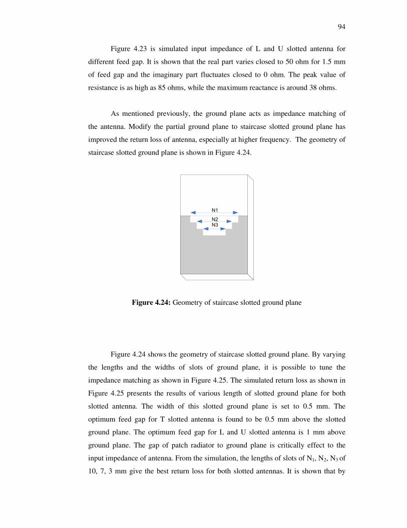
94
Figure 4.23 is simulated input impedance of L and U slotted antenna for
different feed gap. It is shown that the real part varies closed to 50 ohm for 1.5 mm
of feed gap and the imaginary part fluctuates closed to 0 ohm. The peak value of
resistance is as high as 85 ohms, while the maximum reactance is around 38 ohms.
As mentioned previously, the ground plane acts as impedance matching of
the antenna. Modify the partial ground plane to staircase slotted ground plane has
improved the return loss of antenna, especially at higher frequency. The geometry of
staircase slotted ground plane is shown in Figure 4.24.
N3N2
N1
Figure 4.24: Geometry of staircase slotted ground plane
Figure 4.24 shows the geometry of staircase slotted ground plane. By varying
the lengths and the widths of slots of ground plane, it is possible to tune the
impedance matching as shown in Figure 4.25. The simulated return loss as shown in
Figure 4.25 presents the results of various length of slotted ground plane for both
slotted antenna. The width of this slotted ground plane is set to 0.5 mm. The
optimum feed gap for T slotted antenna is found to be 0.5 mm above the slotted
ground plane. The optimum feed gap for L and U slotted antenna is 1 mm above
ground plane. The gap of patch radiator to ground plane is critically effect to the
input impedance of antenna. From the simulation, the lengths of slots of N1, N2, N3 of
10, 7, 3 mm give the best return loss for both slotted antennas. It is shown that by
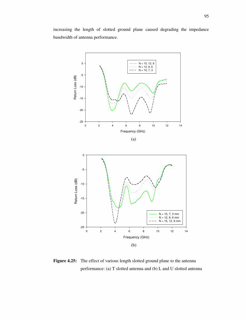
95
increasing the length of slotted ground plane caused degrading the impedance
bandwidth of antenna performance.
Frequency (GHz)
0 2 4 6 8 10 12 14
Retu
rn L
oss (
dB
)
-25
-20
-15
-10
-5
0 N = 15, 12, 9
N = 12, 9, 6
N = 10, 7, 3
(a)
Frequency (GHz)
0 2 4 6 8 10 12 14
Re
turn
Lo
ss (
dB
)
-25
-20
-15
-10
-5
0
N = 10, 7, 3 mm
N = 12, 9, 6 mm
N = 15, 12, 9 mm
(b)
Figure 4.25: The effect of various length slotted ground plane to the antenna
performance: (a) T slotted antenna and (b) L and U slotted antenna
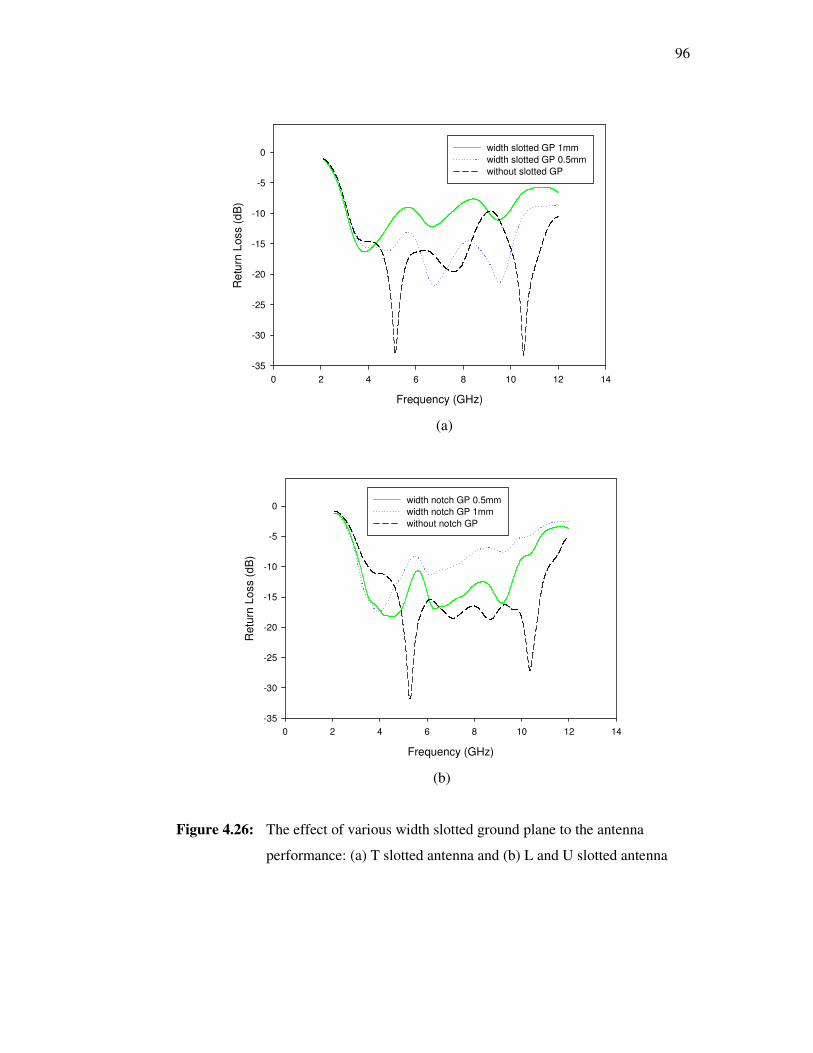
96
Frequency (GHz)
0 2 4 6 8 10 12 14
Re
turn
Loss (
dB
)
-35
-30
-25
-20
-15
-10
-5
0width slotted GP 1mm
width slotted GP 0.5mm
without slotted GP
(a)
Frequency (GHz)
0 2 4 6 8 10 12 14
Retu
rn L
oss (
dB
)
-35
-30
-25
-20
-15
-10
-5
0width notch GP 0.5mm
width notch GP 1mm
without notch GP
(b)
Figure 4.26: The effect of various width slotted ground plane to the antenna
performance: (a) T slotted antenna and (b) L and U slotted antenna
97
Figure 4.26 presents the effect of various width slotted ground plane to the
antenna performance. The width slotted ground plane of 1 mm has degraded the
antenna return loss above -10 dB. This is due to the width slot has brought the
antenna to much more capacitive and far away from the resonance point. The
staircase slotted ground plane has improved the return loss around at 9 GHz for T
slotted antenna with the width slot of 0.5 mm, but this degrade the return loss for L
and U slotted antenna at above 4 GHz. It is also shown that the staircase slotted
ground plane has removed the lower and upper dip resonances for both slotted
antenna. The return loss curves fluctuate around -15 dB. The T slotted with slotted
ground plane antenna cover frequency range of 3.17 GHz to 10.6 GHz with
fractional bandwidth of 108%. The L and U slotted with slotted ground plane
antenna cover 3.17 GHz to 9.8 GHz with fractional bandwidth of 102%.
The simulated return loss curves for various number of slotted ground plane
for both antennas are depicted in Figure 4.27. It is clearly shown that by increasing
the number of slotted ground plane has degraded the antenna performance and led
the antenna to much more capacitive especially at higher frequency range.
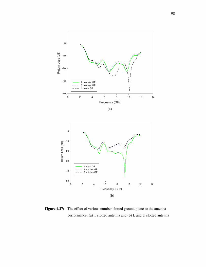
98
Frequency (GHz)
0 2 4 6 8 10 12 14
Re
turn
Lo
ss (
dB
)
-40
-30
-20
-10
0
2 notches GP
3 notches GP
1 notch GP
(a)
Frequency (GHz)
0 2 4 6 8 10 12 14
Re
turn
Lo
ss (
dB
)
-50
-40
-30
-20
-10
0
1 notch GP
2 notches GP
3 notches GP
(b)
Figure 4.27: The effect of various number slotted ground plane to the antenna
performance: (a) T slotted antenna and (b) L and U slotted antenna
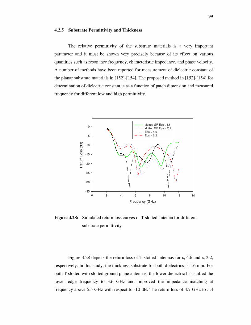
99
4.2.5 Substrate Permittivity and Thickness
The relative permittivity of the substrate materials is a very important
parameter and it must be shown very precisely because of its effect on various
quantities such as resonance frequency, characteristic impedance, and phase velocity.
A number of methods have been reported for measurement of dielectric constant of
the planar substrate materials in [152]-[154]. The proposed method in [152]-[154] for
determination of dielectric constant is as a function of patch dimension and measured
frequency for different low and high permittivity.
Frequency (GHz)
0 2 4 6 8 10 12 14
Re
turn
Lo
ss (
dB
)
-35
-30
-25
-20
-15
-10
-5
0slotted GP Eps =4.6
slotted GP Eps = 2.2
Eps = 4.6
Eps = 2.2
Figure 4.28: Simulated return loss curves of T slotted antenna for different
substrate permittivity
Figure 4.28 depicts the return loss of T slotted antennas for εr 4.6 and εr 2.2,
respectively. In this study, the thickness substrate for both dielectrics is 1.6 mm. For
both T slotted with slotted ground plane antennas, the lower dielectric has shifted the
lower edge frequency to 3.6 GHz and improved the impedance matching at
frequency above 5.5 GHz with respect to -10 dB. The return loss of 4.7 GHz to 5.4
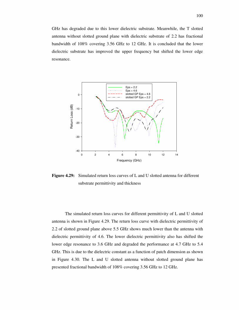
100
GHz has degraded due to this lower dielectric substrate. Meanwhile, the T slotted
antenna without slotted ground plane with dielectric substrate of 2.2 has fractional
bandwidth of 108% covering 3.56 GHz to 12 GHz. It is concluded that the lower
dielectric substrate has improved the upper frequency but shifted the lower edge
resonance.
Frequency (GHz)
0 2 4 6 8 10 12 14
Retu
rn L
oss (
dB
)
-40
-30
-20
-10
0
Eps = 2.2
Eps = 4.6
slotted GP Eps = 4.6
slotted GP Eps = 2.2
Figure 4.29: Simulated return loss curves of L and U slotted antenna for different
substrate permittivity and thickness
The simulated return loss curves for different permittivity of L and U slotted
antenna is shown in Figure 4.29. The return loss curve with dielectric permittivity of
2.2 of slotted ground plane above 5.5 GHz shows much lower than the antenna with
dielectric permittivity of 4.6. The lower dielectric permittivity also has shifted the
lower edge resonance to 3.6 GHz and degraded the performance at 4.7 GHz to 5.4
GHz. This is due to the dielectric constant as a function of patch dimension as shown
in Figure 4.30. The L and U slotted antenna without slotted ground plane has
presented fractional bandwidth of 108% covering 3.56 GHz to 12 GHz.
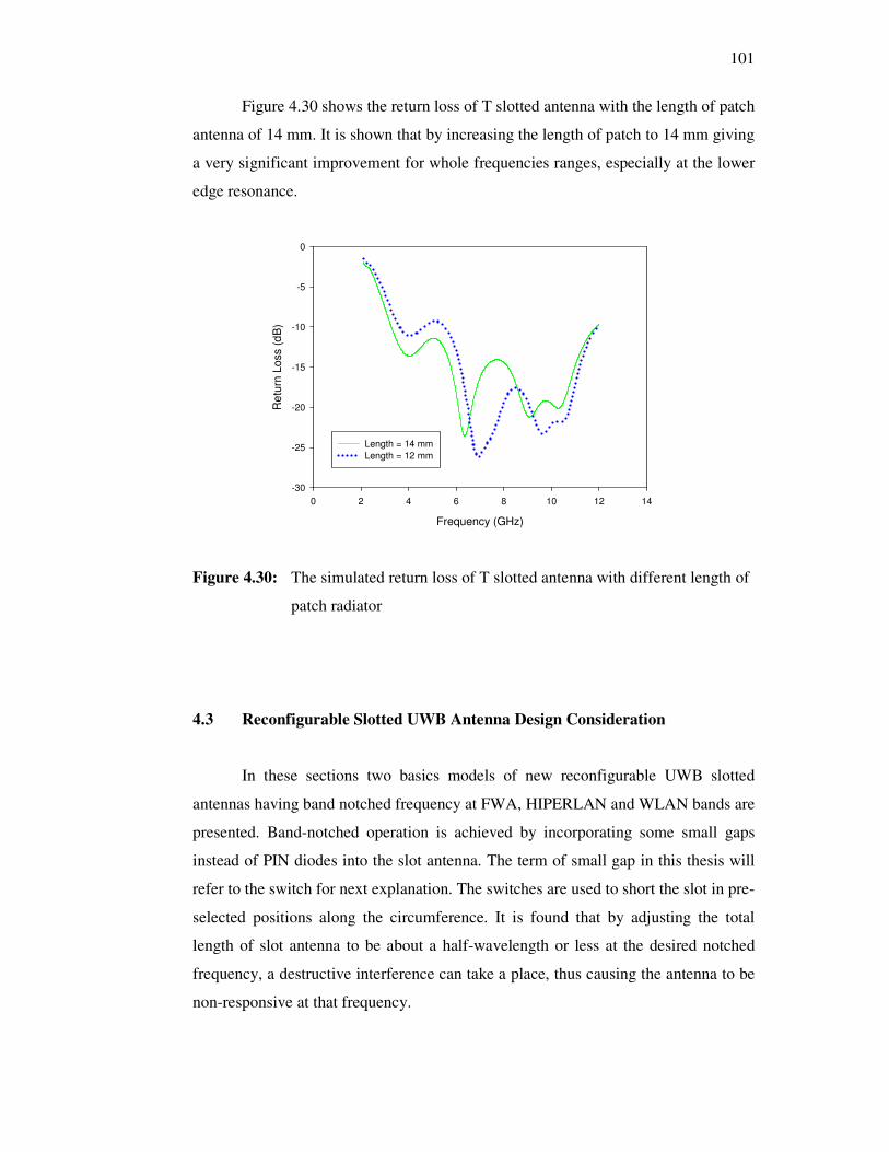
101
Figure 4.30 shows the return loss of T slotted antenna with the length of patch
antenna of 14 mm. It is shown that by increasing the length of patch to 14 mm giving
a very significant improvement for whole frequencies ranges, especially at the lower
edge resonance.
Frequency (GHz)
0 2 4 6 8 10 12 14
Re
turn
Loss (
dB
)
-30
-25
-20
-15
-10
-5
0
Length = 14 mm
Length = 12 mm
Figure 4.30: The simulated return loss of T slotted antenna with different length of
patch radiator
4.3 Reconfigurable Slotted UWB Antenna Design Consideration
In these sections two basics models of new reconfigurable UWB slotted
antennas having band notched frequency at FWA, HIPERLAN and WLAN bands are
presented. Band-notched operation is achieved by incorporating some small gaps
instead of PIN diodes into the slot antenna. The term of small gap in this thesis will
refer to the switch for next explanation. The switches are used to short the slot in pre-
selected positions along the circumference. It is found that by adjusting the total
length of slot antenna to be about a half-wavelength or less at the desired notched
frequency, a destructive interference can take a place, thus causing the antenna to be
non-responsive at that frequency.
102
In this thesis, the switches are used to reconfigure slot element of UWB
antenna for frequency notch tuning. The length of the slot antenna can be lengthened or
shorted by closing or opening the switch allowing for a change in the notched frequency.
For the simulation proposed, the PIN diodes as switches are considered to be ideal
switch. The switches are modeled as small patches that connect or disconnect the
adjacent slot changing the antenna’s slot length. For implementation, the gaps are
created in the UWB antenna pattern, which are represented as switches. The selections of
PIN diodes as switch are based on its low cost, higher speed and it has better insertion
losses at higher frequency than FET switches.
4.3.1 Reconfigurable Modified T Slotted Antenna
In this section, the modified T slotted antenna from the previous model is
used with some switches incorporated into the slot antenna. In order to modify the
previous model to become a reconfigurable notched frequency, the length of inverted
U upper slot is varied and keeps other parameters to be constant. The switches are
modeled as a very small patch with dimension of 0.7 x 1 mm. Thus, this proposed
antenna has double functions as an UWB antenna as well as a frequency notched
antenna without major modification applied.
Figure 4.31 shows the proposed antenna model. The dimension and type of
substrate used is same with the previous model as well as the antenna dimension,
except the dimension for inverted U upper slot. The inverted U slot consists of one
horizontal slot and two verticals slots. To accommodate the proposed notched
frequencies, the length of inverted U upper slot is lengthened than the previous
model. The maximum length of horizontal slot of inverted U upper slot is 11 mm
(TL1), with varying the length of vertical slot based on the proposed notched
frequency. It is investigated that the notched frequency response given only by the
inverted U upper slot rather than other slots. Thus, this simulation is focused on how
the vertical slot affects to the notched frequencies.
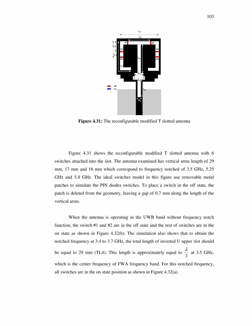
103
TL1
ws
ls1
ls2
ls3
ls4
ls7
off
on
#1 #2
#3 #4
#5 #6
TL2
TL3
TL4
Figure 4.31: The reconfigurable modified T slotted antenna
Figure 4.31 shows the reconfigurable modified T slotted antenna with 6
switches attached into the slot. The antenna examined has vertical arms length of 29
mm, 17 mm and 16 mm which correspond to frequency notched of 3.5 GHz, 5.25
GHz and 5.8 GHz. The ideal switches model in this figure use removable metal
patches to simulate the PIN diodes switches. To place a switch in the off state, the
patch is deleted from the geometry, leaving a gap of 0.7 mm along the length of the
vertical arms.
When the antenna is operating in the UWB band without frequency notch
function, the switch #1 and #2 are in the off state and the rest of switches are in the
on state as shown in Figure 4.32(b). The simulation also shows that to obtain the
notched frequency at 3.4 to 3.7 GHz, the total length of inverted U upper slot should
be equal to 29 mm (TL4). This length is approximately equal to 3
λ at 3.5 GHz,
which is the center frequency of FWA frequency band. For this notched frequency,
all switches are in the on state position as shown in Figure 4.32(a).
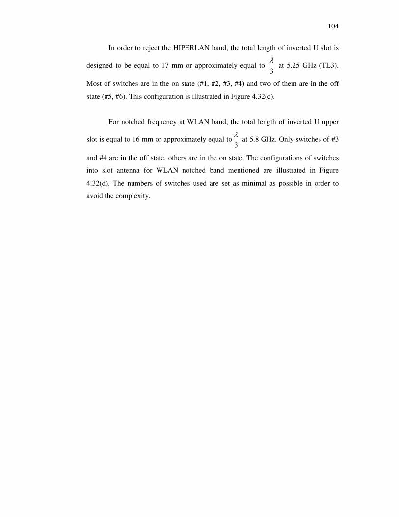
104
In order to reject the HIPERLAN band, the total length of inverted U slot is
designed to be equal to 17 mm or approximately equal to 3
λ at 5.25 GHz (TL3).
Most of switches are in the on state (#1, #2, #3, #4) and two of them are in the off
state (#5, #6). This configuration is illustrated in Figure 4.32(c).
For notched frequency at WLAN band, the total length of inverted U upper
slot is equal to 16 mm or approximately equal to3
λ at 5.8 GHz. Only switches of #3
and #4 are in the off state, others are in the on state. The configurations of switches
into slot antenna for WLAN notched band mentioned are illustrated in Figure
4.32(d). The numbers of switches used are set as minimal as possible in order to
avoid the complexity.
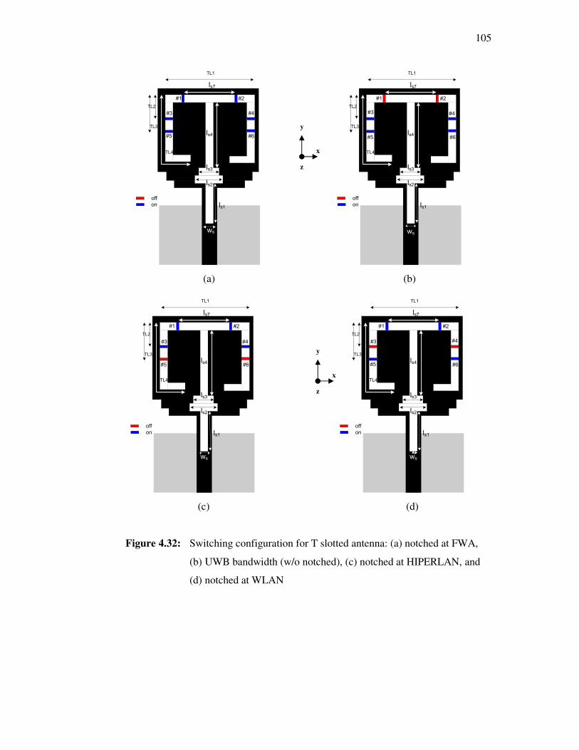
105
TL1
ws
ls1
ls2
ls3
ls4
ls7
off
on
#1 #2
#3 #4
#5 #6
TL2
TL3
TL4
TL1
ws
ls1
ls2
ls3
ls4
ls7
off
on
#1 #2
#3 #4
#5 #6
TL2
TL3
TL4
(a) (b)
TL1
ws
ls1
ls2
ls3
ls4
ls7
off
on
#1 #2
#3 #4
#5 #6
TL2
TL3
TL4
ws
ls1
ls2
ls3
ls4
ls7
off
on
#1 #2
#3 #4
#5 #6
TL1
TL2
TL3
TL4
(c) (d)
Figure 4.32: Switching configuration for T slotted antenna: (a) notched at FWA,
(b) UWB bandwidth (w/o notched), (c) notched at HIPERLAN, and
(d) notched at WLAN
y
x
z
y
x
z
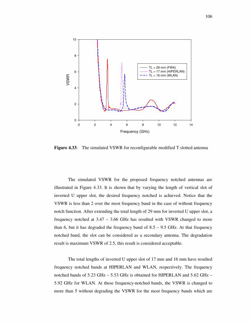
106
Frequency (GHz)
0 2 4 6 8 10 12 14
VS
WR
0
2
4
6
8
10
TL = 29 mm (FWA)
TL = 17 mm (HIPERLAN)
TL = 16 mm (WLAN)
Figure 4.33: The simulated VSWR for reconfigurable modified T slotted antenna
The simulated VSWR for the proposed frequency notched antennas are
illustrated in Figure 4.33. It is shown that by varying the length of vertical slot of
inverted U upper slot, the desired frequency notched is achieved. Notice that the
VSWR is less than 2 over the most frequency band in the case of without frequency
notch function. After extending the total length of 29 mm for inverted U upper slot, a
frequency notched at 3.47 – 3.66 GHz has resulted with VSWR changed to more
than 6, but it has degraded the frequency band of 8.5 – 9.5 GHz. At that frequency
notched band, the slot can be considered as a secondary antenna. The degradation
result is maximum VSWR of 2.5, this result is considered acceptable.
The total lengths of inverted U upper slot of 17 mm and 16 mm have resulted
frequency notched bands at HIPERLAN and WLAN, respectively. The frequency
notched bands of 5.23 GHz – 5.53 GHz is obtained for HIPERLAN and 5.62 GHz –
5.92 GHz for WLAN. At these frequency-notched bands, the VSWR is changed to
more than 5 without degrading the VSWR for the most frequency bands which are
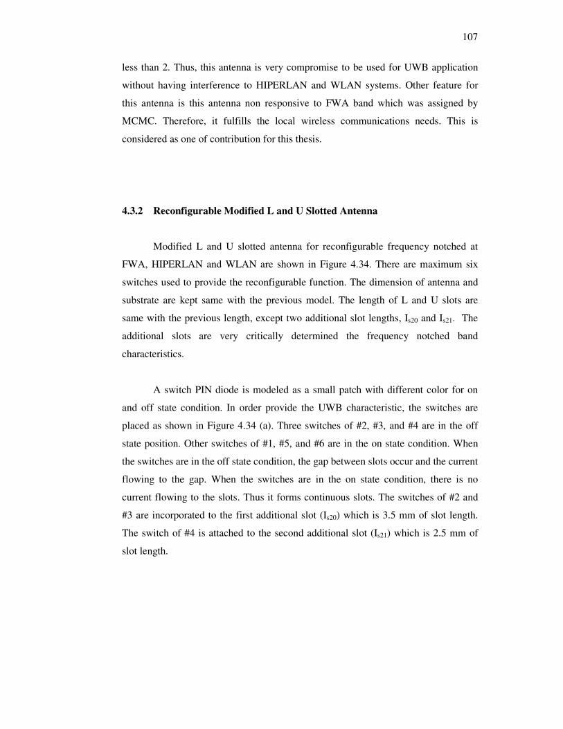
107
less than 2. Thus, this antenna is very compromise to be used for UWB application
without having interference to HIPERLAN and WLAN systems. Other feature for
this antenna is this antenna non responsive to FWA band which was assigned by
MCMC. Therefore, it fulfills the local wireless communications needs. This is
considered as one of contribution for this thesis.
4.3.2 Reconfigurable Modified L and U Slotted Antenna
Modified L and U slotted antenna for reconfigurable frequency notched at
FWA, HIPERLAN and WLAN are shown in Figure 4.34. There are maximum six
switches used to provide the reconfigurable function. The dimension of antenna and
substrate are kept same with the previous model. The length of L and U slots are
same with the previous length, except two additional slot lengths, Is20 and Is21. The
additional slots are very critically determined the frequency notched band
characteristics.
A switch PIN diode is modeled as a small patch with different color for on
and off state condition. In order provide the UWB characteristic, the switches are
placed as shown in Figure 4.34 (a). Three switches of #2, #3, and #4 are in the off
state position. Other switches of #1, #5, and #6 are in the on state condition. When
the switches are in the off state condition, the gap between slots occur and the current
flowing to the gap. When the switches are in the on state condition, there is no
current flowing to the slots. Thus it forms continuous slots. The switches of #2 and
#3 are incorporated to the first additional slot (Is20) which is 3.5 mm of slot length.
The switch of #4 is attached to the second additional slot (Is21) which is 2.5 mm of
slot length.
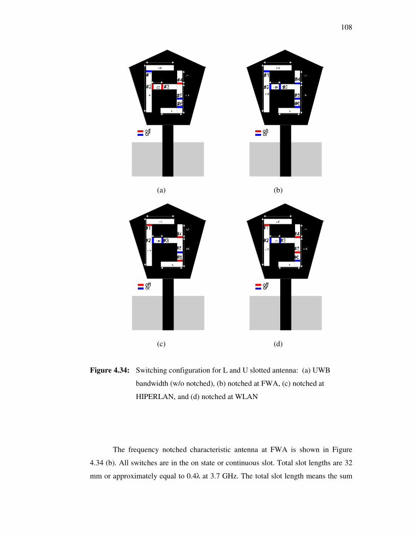
108
(a) (b)
(c) (d)
Figure 4.34: Switching configuration for L and U slotted antenna: (a) UWB
bandwidth (w/o notched), (b) notched at FWA, (c) notched at
HIPERLAN, and (d) notched at WLAN
The frequency notched characteristic antenna at FWA is shown in Figure
4.34 (b). All switches are in the on state or continuous slot. Total slot lengths are 32
mm or approximately equal to 0.4λ at 3.7 GHz. The total slot length means the sum
109
of slot lengths of L, U and additional slots. Figure 4.34 (c) and Figure 4.34 (d)
present the frequency notched characteristic antenna at HIPERLAN and WLAN,
respectively. To reject interference from HIPERLAN, the switches of #1, #4, and #6
are in the off state while switches of #2, #3, and #5 are in the on state. It is
investigated that by inserting those switches in the off state condition broke the
connection between slots. This break connection has reduced the slot length to be
20.75 mm or approximately equal to 0.33λ at 5.2 GHz. Thus, the antenna has
frequency notched at HIPERLAN band. The total slot length is measured from the
connecting slots.
The configuration of switches in Figure 4.34(d) have resulted an antenna with
frequency notched at WLAN. It is shown that the switch of #5 set in the off state in
order to reduce the slot length, while the switch of #6 is in the on state. This is the
only different while compared to the HIPERLAN configuration. Total slot lengths
are 18 mm or approximately equal to 0.33λ at 5.75 GHz measured from the
connecting slots.
Frequency (GHz)
0 2 4 6 8 10 12 14
VS
WR
0
2
4
6
8
10
Notched at FWA
Notched at HIPERLAN
Notched at WLAN
Figure 4.35: The simulated VSWR for reconfigurable modified L and U slotted
antenna
110
Figure 4.35 shows the simulated VSWR for reconfigurable modified L and U
slotted antenna. By varying the slot lengths and break the connection between slots
using switches, the proposed frequency notched is achieved. The FWA notched
bands are obtained from 3.57 GHz – 3.86 GHz with the total slot length of 32 mm at
3.7 GHz, which is the centre frequency. While the HIPERLAN and WLAN notched
bands are from 4.84 GHz to 5.33 GHz and 5.53 GHz to 6.02 GHz, respectively. It is
noted that beyond the frequency notched bands, the VSWR is kept to be less than 2.
4.4 Summary
In this chapter, various polygonal UWB antennas have been presented with
some parameters design taken into consideration. There are two models UWB slotted
antennas resulted in this study, such as T slotted antenna with slotted ground plane
and L and U slotted antenna. Both antennas show a very broad bandwidth and nearly
omni directional pattern. Both antennas show a very good radiation and antenna
efficiency within UWB frequency range which exceed 75% except at 12 GHz. This
chapter also investigates the reconfigurable characteristic for proposed UWB
antennas by inserting the half-wavelength slot to the patch. These proposed types of
antennas are variation from the previous models. The reconfigurability behaviors are
achieved by shortened or widened the slot. The switching is model as a small patch
of 0.7 mm x 1 mm instead of PIN diodes.
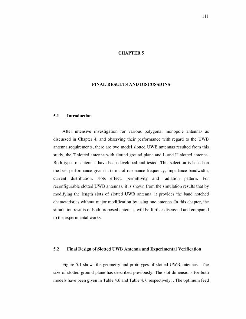
111
CHAPTER 5
FINAL RESULTS AND DISCUSSIONS
5.1 Introduction
After intensive investigation for various polygonal monopole antennas as
discussed in Chapter 4, and observing their performance with regard to the UWB
antenna requirements, there are two model slotted UWB antennas resulted from this
study, the T slotted antenna with slotted ground plane and L and U slotted antenna.
Both types of antennas have been developed and tested. This selection is based on
the best performance given in terms of resonance frequency, impedance bandwidth,
current distribution, slots effect, permittivity and radiation pattern. For
reconfigurable slotted UWB antennas, it is shown from the simulation results that by
modifying the length slots of slotted UWB antenna, it provides the band notched
characteristics without major modification by using one antenna. In this chapter, the
simulation results of both proposed antennas will be further discussed and compared
to the experimental works.
5.2 Final Design of Slotted UWB Antenna and Experimental Verification
Figure 5.1 shows the geometry and prototypes of slotted UWB antennas. The
size of slotted ground plane has described previously. The slot dimensions for both
models have been given in Table 4.6 and Table 4.7, respectively. . The optimum feed
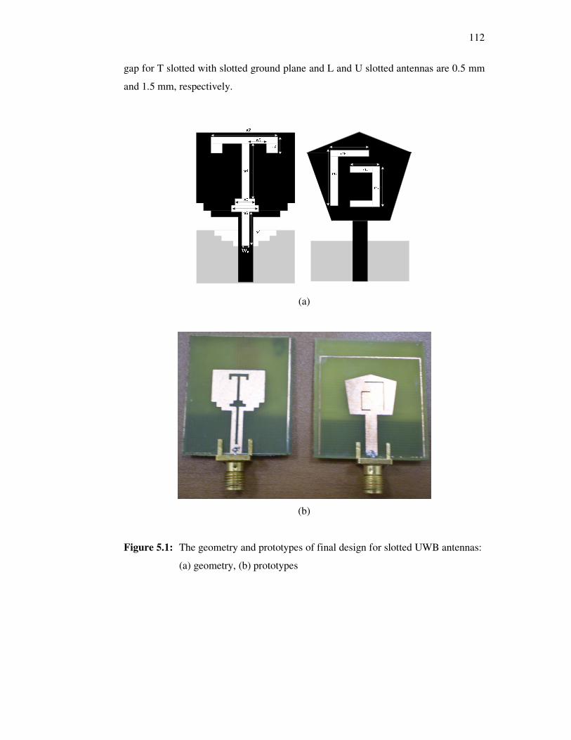
112
gap for T slotted with slotted ground plane and L and U slotted antennas are 0.5 mm
and 1.5 mm, respectively.
(a)
(b)
Figure 5.1: The geometry and prototypes of final design for slotted UWB antennas:
(a) geometry, (b) prototypes
113
As shown in Figure 5.1, both prototypes are printed in the front of substrate
FR4 of thickness 1.6 mm and relative permittivity (εr) 4.6. The return losses were
measured by using Agilent 8722 ES network analyzer. The measured of both
prototypes and simulated return loss curves are plotted in Figure 5.2 and Figure 5.3,
respectively. The return loss predicted by the FDTD solutions is reasonably close to
the measured values.
5.2.1 Simulated and Measured Return Loss
As shown in Figure 5.2, the measured return loss curves for both T slotted
antennas with and without slotted ground plane are reasonably close to the simulated
results. It is shown that both results have produced multiple resonances frequencies,
which shifted from the simulated resonances, but they are still covering the UWB
bandwidth requirement. For T slotted antenna with slotted ground plane as shown in
Figure 5.2(a), the frequency ranges cover 3 GHz to 10.23 GHz with respect to -10 dB
of return loss. While the second antenna without slotted ground plane as shown in
Figure 5.2(b), the return loss covers 2.3 GHz to 10.4 GHz. From this measured
results, the antenna without slotted ground plane is better than the antenna with
slotted ground plane in terms of the impedance bandwidth. This is due to the antenna
with slotted ground plane need very accuracy in alignment between the slotted
ground plane and patch on both sided of substrate during fabrication. The distance of
patch to the ground plane is also very small of 0.5 mm. The misalignment occurred
affects the impedance bandwidth. The measurements confirm the UWB
characteristic of the proposed slotted UWB antennas, as predicted in the simulations.
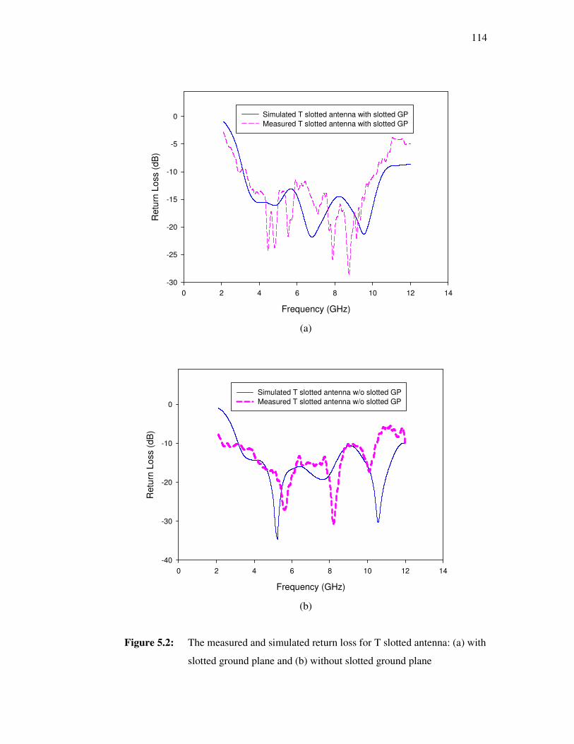
114
Frequency (GHz)
0 2 4 6 8 10 12 14
Retu
rn L
oss (
dB
)
-30
-25
-20
-15
-10
-5
0 Simulated T slotted antenna with slotted GP
Measured T slotted antenna with slotted GP
(a)
Frequency (GHz)
0 2 4 6 8 10 12 14
Retu
rn L
oss (
dB
)
-40
-30
-20
-10
0
Simulated T slotted antenna w/o slotted GP
Measured T slotted antenna w/o slotted GP
(b)
Figure 5.2: The measured and simulated return loss for T slotted antenna: (a) with
slotted ground plane and (b) without slotted ground plane
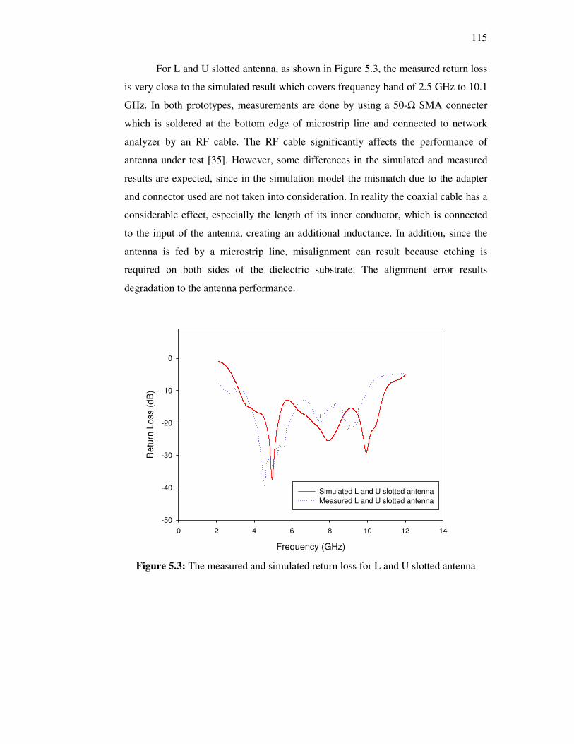
115
For L and U slotted antenna, as shown in Figure 5.3, the measured return loss
is very close to the simulated result which covers frequency band of 2.5 GHz to 10.1
GHz. In both prototypes, measurements are done by using a 50-Ω SMA connecter
which is soldered at the bottom edge of microstrip line and connected to network
analyzer by an RF cable. The RF cable significantly affects the performance of
antenna under test [35]. However, some differences in the simulated and measured
results are expected, since in the simulation model the mismatch due to the adapter
and connector used are not taken into consideration. In reality the coaxial cable has a
considerable effect, especially the length of its inner conductor, which is connected
to the input of the antenna, creating an additional inductance. In addition, since the
antenna is fed by a microstrip line, misalignment can result because etching is
required on both sides of the dielectric substrate. The alignment error results
degradation to the antenna performance.
Frequency (GHz)
0 2 4 6 8 10 12 14
Re
turn
Loss (
dB
)
-50
-40
-30
-20
-10
0
Simulated L and U slotted antenna
Measured L and U slotted antenna
Figure 5.3: The measured and simulated return loss for L and U slotted antenna
116
From experimental experiences, the multiple resonances of return loss
occurred on the proposed antennas are due to these antennas printed in the front of
FR4 substrate. It has been investigated during the return loss measurement of many
wideband antennas that have been developed. In addition, the FR4 substrate quality
needs to be taken into consideration. It should be used within six months after
purchased in order to avoid the oxidation process. The poor quality of FR4 substrate
used produces a poor measured return loss and need longer time during etching
process. Thus, perfect impedance match is not easily obtainable. These fabrication
processes are important, because a slight error could result in major degradation in
antenna performance.
5.2.2 Simulated and Measured VSWR
The VSWR for both prototypes were computed and measured as well and
shown in Figure 5.4. The agreement between measured and calculated results
indicates that accurate design studies can be performed by simulation. The VSWR
curves are referenced to a 50-Ω input impedance in both simulation and
measurement. The VSWRs are well below 2:1 achieved by tapering the bottom of
the patch and properly designed on the gap to the ground plane.
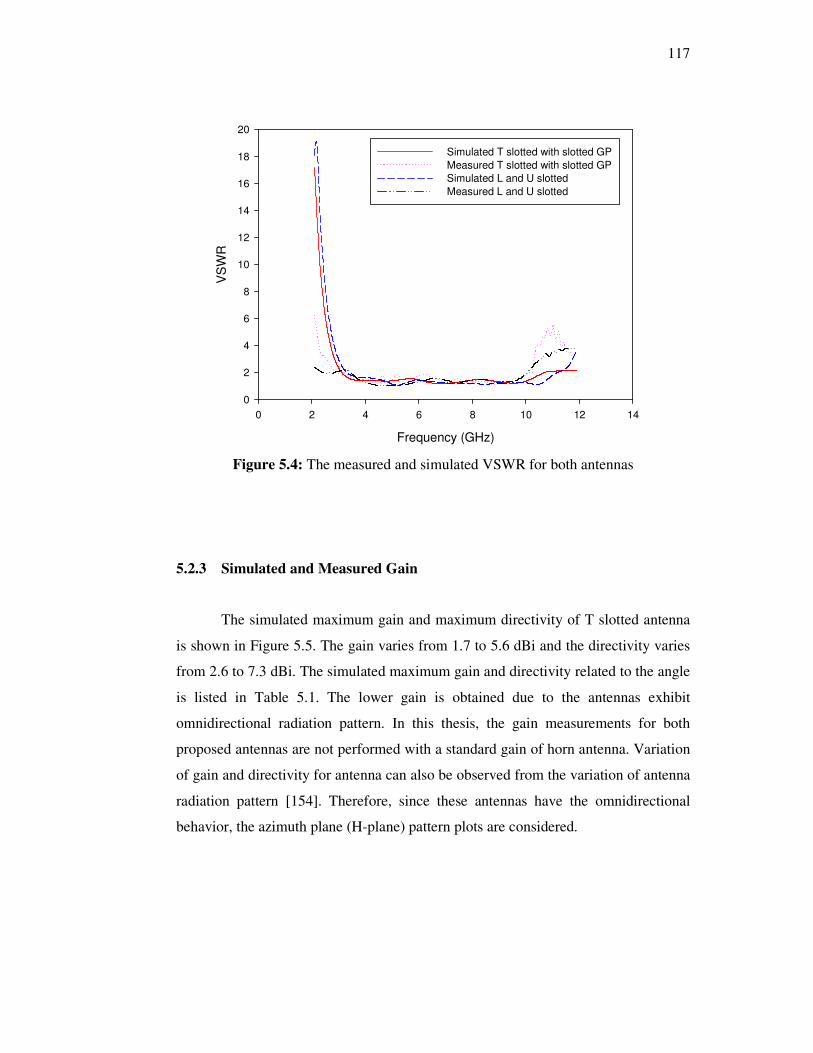
117
Frequency (GHz)
0 2 4 6 8 10 12 14
VS
WR
0
2
4
6
8
10
12
14
16
18
20
Simulated T slotted with slotted GP
Measured T slotted with slotted GP
Simulated L and U slotted
Measured L and U slotted
Figure 5.4: The measured and simulated VSWR for both antennas
5.2.3 Simulated and Measured Gain
The simulated maximum gain and maximum directivity of T slotted antenna
is shown in Figure 5.5. The gain varies from 1.7 to 5.6 dBi and the directivity varies
from 2.6 to 7.3 dBi. The simulated maximum gain and directivity related to the angle
is listed in Table 5.1. The lower gain is obtained due to the antennas exhibit
omnidirectional radiation pattern. In this thesis, the gain measurements for both
proposed antennas are not performed with a standard gain of horn antenna. Variation
of gain and directivity for antenna can also be observed from the variation of antenna
radiation pattern [154]. Therefore, since these antennas have the omnidirectional
behavior, the azimuth plane (H-plane) pattern plots are considered.
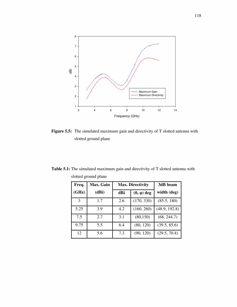
118
Frequency (GHz)
2 4 6 8 10 12 14
dB
i
1
2
3
4
5
6
7
8
Maximum Gain
Maximum Directivity
Figure 5.5: The simulated maximum gain and directivity of T slotted antenna with
slotted ground plane
Table 5.1: The simulated maximum gain and directivity of T slotted antenna with
slotted ground plane
Max. Directivity Freq.
(GHz)
Max. Gain
(dBi) dBi (θ, φ) deg
3dB beam
width (deg)
3 1.7 2.6 (170, 330) (85.5, 180)
5.25 3.9 4.2 (160, 260) (48.9, 192.8)
7.5 2.7 3.1 (80,150) (68, 244.7)
9.75 5.5 6.4 (80, 120) (39.5, 85.6)
12 5.6 7.3 (90, 120) (29.5, 70.4)
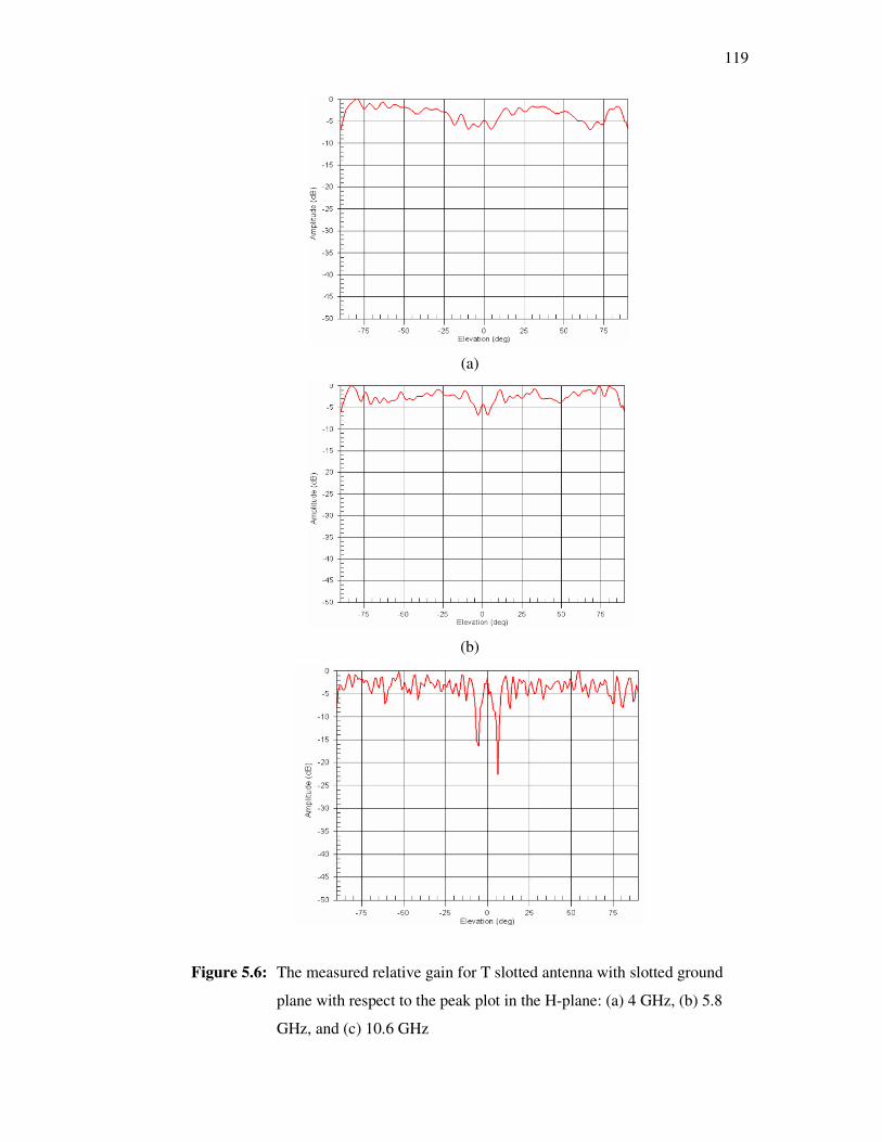
119
(a)
(b)
Figure 5.6: The measured relative gain for T slotted antenna with slotted ground
plane with respect to the peak plot in the H-plane: (a) 4 GHz, (b) 5.8
GHz, and (c) 10.6 GHz
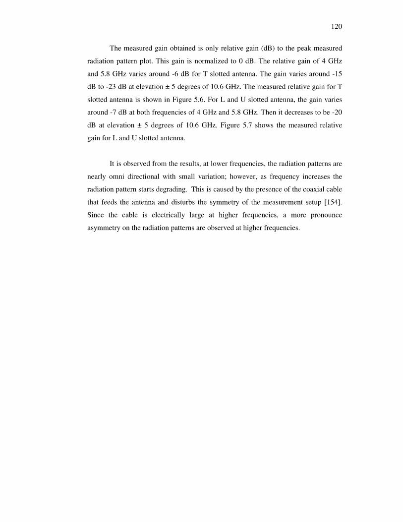
120
The measured gain obtained is only relative gain (dB) to the peak measured
radiation pattern plot. This gain is normalized to 0 dB. The relative gain of 4 GHz
and 5.8 GHz varies around -6 dB for T slotted antenna. The gain varies around -15
dB to -23 dB at elevation ± 5 degrees of 10.6 GHz. The measured relative gain for T
slotted antenna is shown in Figure 5.6. For L and U slotted antenna, the gain varies
around -7 dB at both frequencies of 4 GHz and 5.8 GHz. Then it decreases to be -20
dB at elevation ± 5 degrees of 10.6 GHz. Figure 5.7 shows the measured relative
gain for L and U slotted antenna.
It is observed from the results, at lower frequencies, the radiation patterns are
nearly omni directional with small variation; however, as frequency increases the
radiation pattern starts degrading. This is caused by the presence of the coaxial cable
that feeds the antenna and disturbs the symmetry of the measurement setup [154].
Since the cable is electrically large at higher frequencies, a more pronounce
asymmetry on the radiation patterns are observed at higher frequencies.
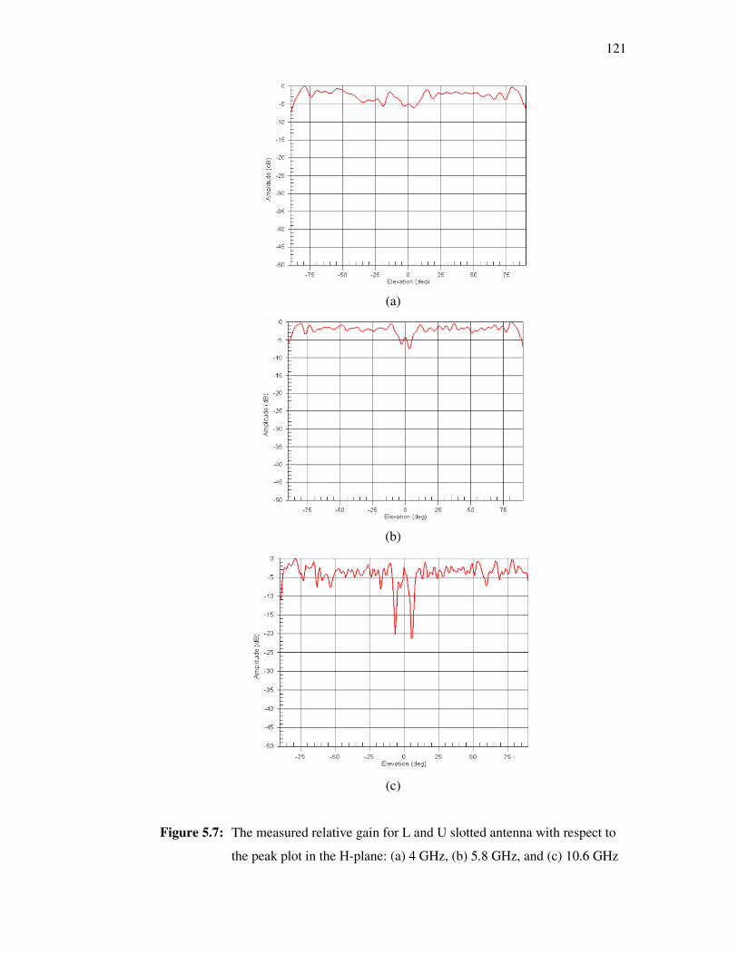
121
(a)
(b)
(c)
Figure 5.7: The measured relative gain for L and U slotted antenna with respect to
the peak plot in the H-plane: (a) 4 GHz, (b) 5.8 GHz, and (c) 10.6 GHz
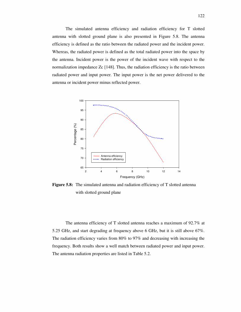
122
The simulated antenna efficiency and radiation efficiency for T slotted
antenna with slotted ground plane is also presented in Figure 5.8. The antenna
efficiency is defined as the ratio between the radiated power and the incident power.
Whereas, the radiated power is defined as the total radiated power into the space by
the antenna. Incident power is the power of the incident wave with respect to the
normalization impedance Zc [148]. Thus, the radiation efficiency is the ratio between
radiated power and input power. The input power is the net power delivered to the
antenna or incident power minus reflected power.
Frequency (GHz)
2 4 6 8 10 12 14
Perc
enta
ge (
%)
65
70
75
80
85
90
95
100
Antenna efficiency
Radiation efficiency
Figure 5.8: The simulated antenna and radiation efficiency of T slotted antenna
with slotted ground plane
The antenna efficiency of T slotted antenna reaches a maximum of 92.7% at
5.25 GHz, and start degrading at frequency above 6 GHz, but it is still above 67%.
The radiation efficiency varies from 80% to 97% and decreasing with increasing the
frequency. Both results show a well match between radiated power and input power.
The antenna radiation properties are listed in Table 5.2.
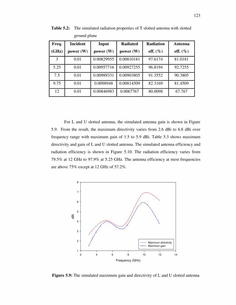
123
Table 5.2: The simulated radiation properties of T slotted antenna with slotted
ground plane
Freq.
(GHz)
Incident
power (W)
Input
power (W)
Radiated
power (W)
Radiation
eff. (%)
Antenna
eff. (%)
3 0.01 0.00829955 0.00810181 97.6174 81.0181
5.25 0.01 0.00957716 0.00927255 96.8194 92.7255
7.5 0.01 0.00989331 0.00903805 91.3552 90.3805
9.75 0.01 0.0098948 0.00814509 82.3169 81.4509
12 0.01 0.00846983 0.0067767 80.0098 67.767
For L and U slotted antenna, the simulated antenna gain is shown in Figure
5.9. From the result, the maximum directivity varies from 2.6 dBi to 6.8 dBi over
frequency range with maximum gain of 1.5 to 5.9 dBi. Table 5.3 shows maximum
directivity and gain of L and U slotted antenna. The simulated antenna efficiency and
radiation efficiency is shown in Figure 5.10. The radiation efficiency varies from
79.5% at 12 GHz to 97.9% at 5.25 GHz. The antenna efficiency at most frequencies
are above 75% except at 12 GHz of 57.2%.
Frequency (GHz)
2 4 6 8 10 12 14
dB
i
1
2
3
4
5
6
7
8
Maximum directivity
Maximum gain
Figure 5.9: The simulated maximum gain and directivity of L and U slotted antenna
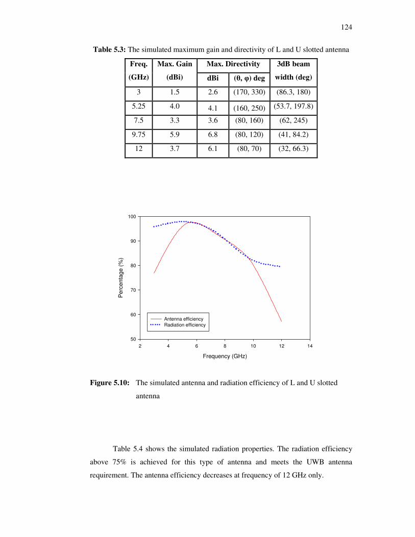
124
Table 5.3: The simulated maximum gain and directivity of L and U slotted antenna
Max. Directivity Freq.
(GHz)
Max. Gain
(dBi) dBi (θ, φ) deg
3dB beam
width (deg)
3 1.5 2.6 (170, 330) (86.3, 180)
5.25 4.0 4.1 (160, 250) (53.7, 197.8)
7.5 3.3 3.6 (80, 160) (62, 245)
9.75 5.9 6.8 (80, 120) (41, 84.2)
12 3.7 6.1 (80, 70) (32, 66.3)
Frequency (GHz)
2 4 6 8 10 12 14
Pe
rce
nta
ge (
%)
50
60
70
80
90
100
Antenna efficiency
Radiation efficiency
Figure 5.10: The simulated antenna and radiation efficiency of L and U slotted
antenna
Table 5.4 shows the simulated radiation properties. The radiation efficiency
above 75% is achieved for this type of antenna and meets the UWB antenna
requirement. The antenna efficiency decreases at frequency of 12 GHz only.
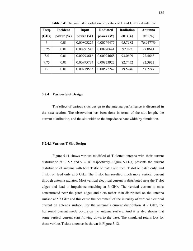
125
Table 5.4: The simulated radiation properties of L and U slotted antenna
Freq.
(GHz)
Incident
power (W)
Input
power (W)
Radiated
power (W)
Radiation
eff. (%)
Antenna
eff. (%)
3 0.01 0.00803227 0.00769477 95.7982 76.9477%
5.25 0.01 0.00991543 0.00970641 97.892 97.0641
7.5 0.01 0.00993616 0.00924668 93.0609 92.4668
9.75 0.01 0.00995734 0.00823922 82.7452 82.3922
12 0.01 0.00719585 0.00572247 79.5246 57.2247
5.2.4 Various Slot Design
The effect of various slots design to the antenna performance is discussed in
the next section. The observation has been done in terms of the slot length, the
current distribution, and the slot width to the impedance bandwidth by simulation.
5.2.4.1 Various T Slot Design
Figure 5.11 shows various modified of T slotted antenna with their current
distribution at 3, 5.5 and 9 GHz, respectively. Figure 5.11(a) presents the current
distribution of antenna with both T slot on patch and feed, T slot on patch only, and
T slot on feed only at 3 GHz. The T slot has resulted much more vertical current
through antenna radiator. Most vertical electrical current is distributed near the T slot
edges and lead to impedance matching at 3 GHz. The vertical current is most
concentrated near the patch edges and slots rather than distributed on the antenna
surface at 5.5 GHz and this cause the decrement of the intensity of vertical electrical
current on antenna surface. For the antenna’s current distribution at 9 GHz, the
horizontal current mode occurs on the antenna surface. And it is also shown that
some vertical current start flowing down to the base. The simulated return loss for
these various T slots antennas is shown in Figure 5.12.
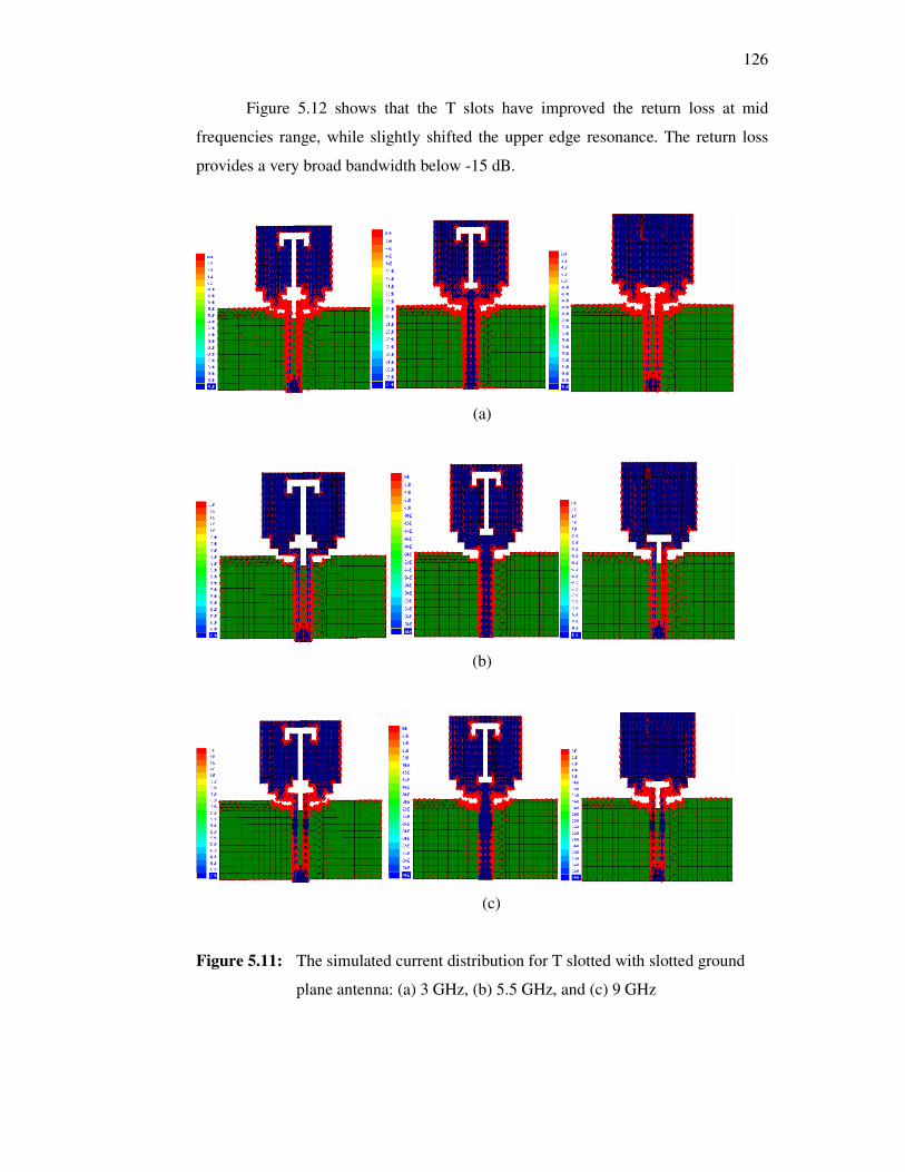
126
Figure 5.12 shows that the T slots have improved the return loss at mid
frequencies range, while slightly shifted the upper edge resonance. The return loss
provides a very broad bandwidth below -15 dB.
(a)
(b)
(c)
Figure 5.11: The simulated current distribution for T slotted with slotted ground
plane antenna: (a) 3 GHz, (b) 5.5 GHz, and (c) 9 GHz
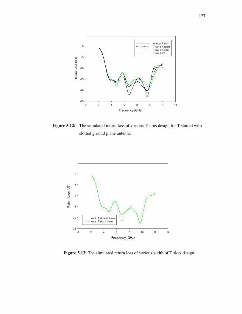
127
Frequency (GHz)
0 2 4 6 8 10 12 14
Re
turn
Lo
ss (
dB
)
-25
-20
-15
-10
-5
0without T slot
T slot on patch
T slot on feed
T slot both
Figure 5.12: The simulated return loss of various T slots design for T slotted with
slotted ground plane antenna
Frequency (GHz)
0 2 4 6 8 10 12 14
Retu
rn L
oss (
dB
)
-25
-20
-15
-10
-5
0
width T slot= 0.5 mm
width T slot = 1mm
Figure 5.13: The simulated return loss of various width of T slots design
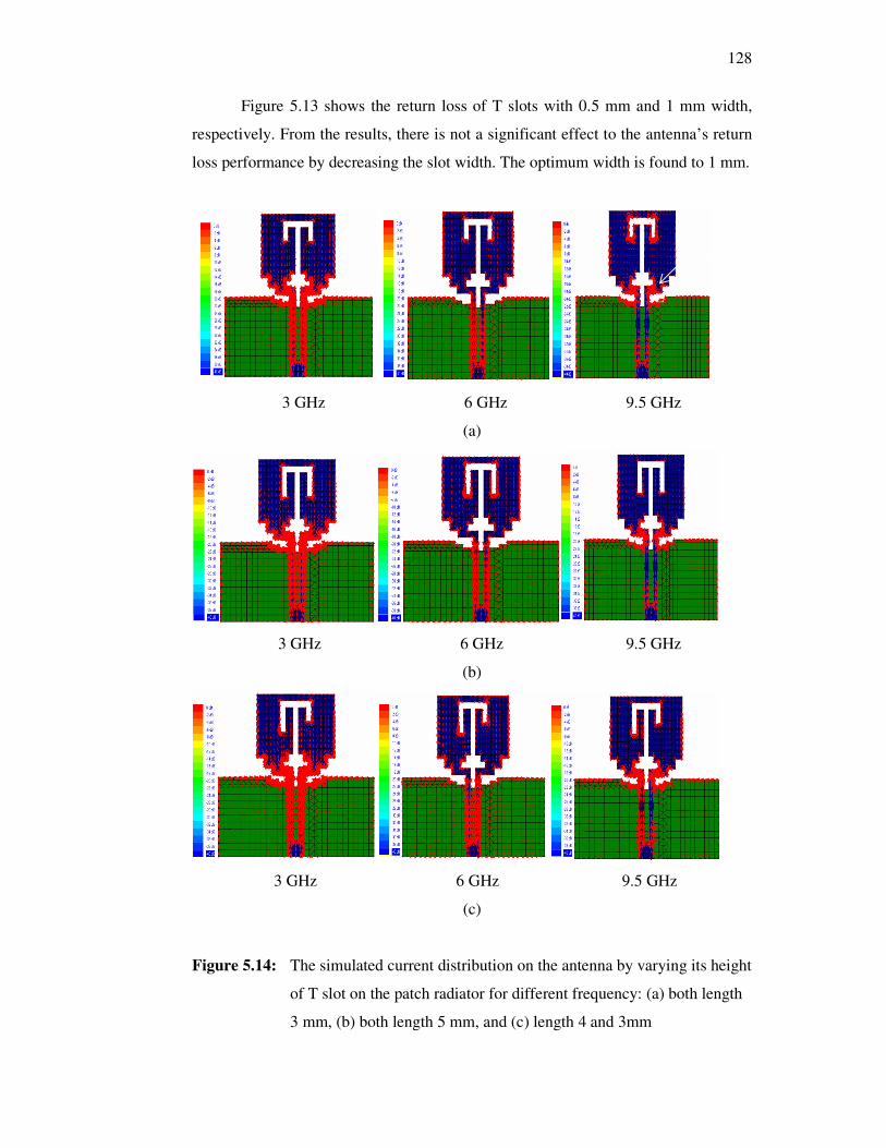
128
Figure 5.13 shows the return loss of T slots with 0.5 mm and 1 mm width,
respectively. From the results, there is not a significant effect to the antenna’s return
loss performance by decreasing the slot width. The optimum width is found to 1 mm.
3 GHz 6 GHz 9.5 GHz
(a)
3 GHz 6 GHz 9.5 GHz
(b)
3 GHz 6 GHz 9.5 GHz
(c)
Figure 5.14: The simulated current distribution on the antenna by varying its height
of T slot on the patch radiator for different frequency: (a) both length
3 mm, (b) both length 5 mm, and (c) length 4 and 3mm
Y
X
Z
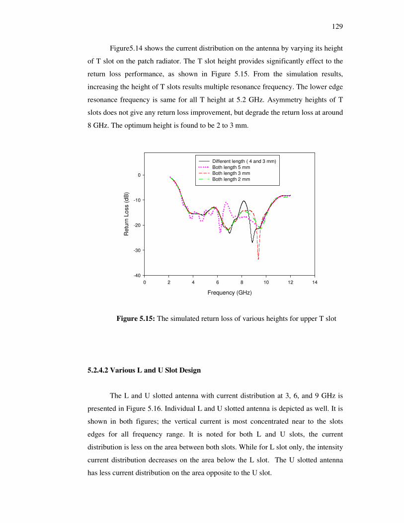
129
Figure5.14 shows the current distribution on the antenna by varying its height
of T slot on the patch radiator. The T slot height provides significantly effect to the
return loss performance, as shown in Figure 5.15. From the simulation results,
increasing the height of T slots results multiple resonance frequency. The lower edge
resonance frequency is same for all T height at 5.2 GHz. Asymmetry heights of T
slots does not give any return loss improvement, but degrade the return loss at around
8 GHz. The optimum height is found to be 2 to 3 mm.
Frequency (GHz)
0 2 4 6 8 10 12 14
Retu
rn L
oss (
dB
)
-40
-30
-20
-10
0
Different length ( 4 and 3 mm)
Both length 5 mm
Both length 3 mm
Both length 2 mm
Figure 5.15: The simulated return loss of various heights for upper T slot
5.2.4.2 Various L and U Slot Design
The L and U slotted antenna with current distribution at 3, 6, and 9 GHz is
presented in Figure 5.16. Individual L and U slotted antenna is depicted as well. It is
shown in both figures; the vertical current is most concentrated near to the slots
edges for all frequency range. It is noted for both L and U slots, the current
distribution is less on the area between both slots. While for L slot only, the intensity
current distribution decreases on the area below the L slot. The U slotted antenna
has less current distribution on the area opposite to the U slot.
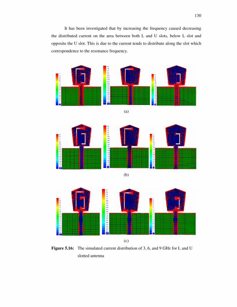
130
It has been investigated that by increasing the frequency caused decreasing
the distributed current on the area between both L and U slots, below L slot and
opposite the U slot. This is due to the current tends to distribute along the slot which
correspondence to the resonance frequency.
(a)
(b)
(c)
Figure 5.16: The simulated current distribution of 3, 6, and 9 GHz for L and U
slotted antenna
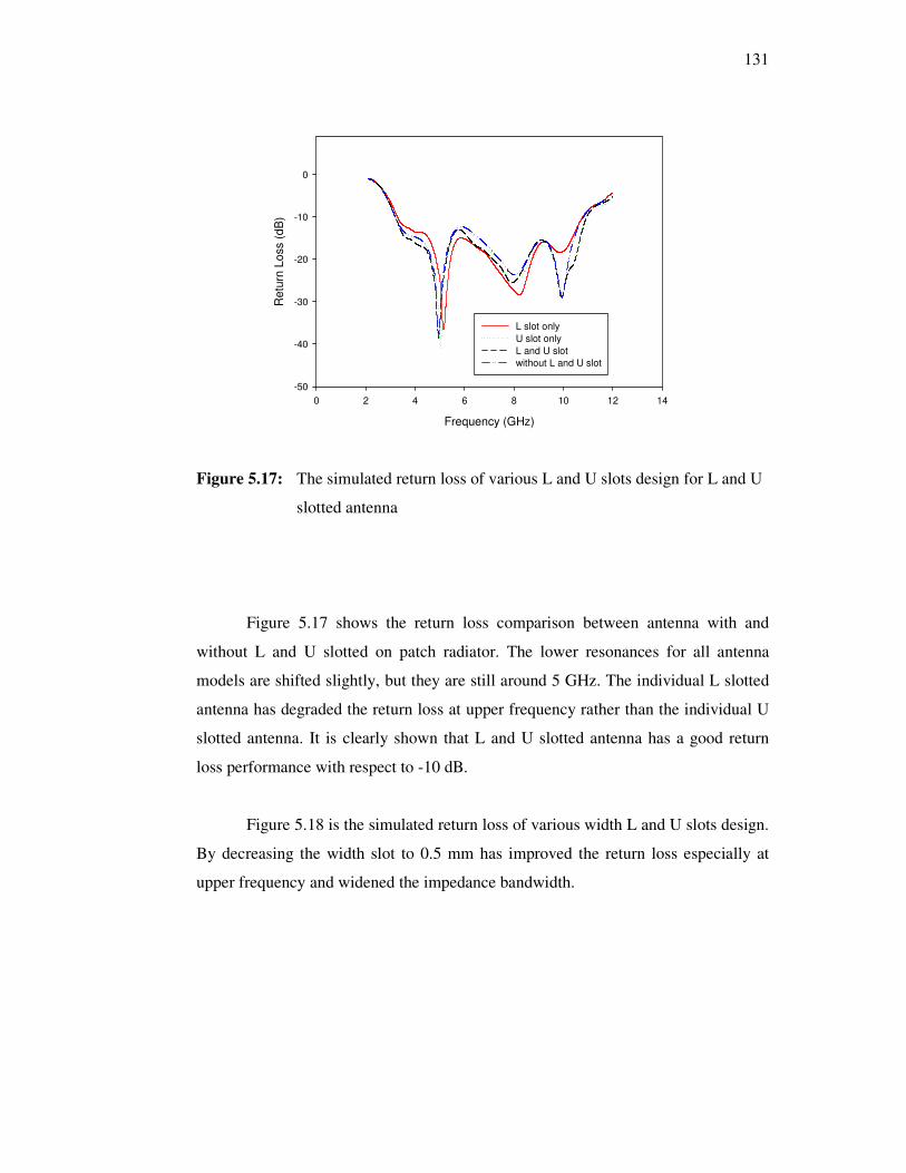
131
Frequency (GHz)
0 2 4 6 8 10 12 14
Re
turn
Lo
ss (
dB
)
-50
-40
-30
-20
-10
0
L slot only
U slot only
L and U slot
without L and U slot
Figure 5.17: The simulated return loss of various L and U slots design for L and U
slotted antenna
Figure 5.17 shows the return loss comparison between antenna with and
without L and U slotted on patch radiator. The lower resonances for all antenna
models are shifted slightly, but they are still around 5 GHz. The individual L slotted
antenna has degraded the return loss at upper frequency rather than the individual U
slotted antenna. It is clearly shown that L and U slotted antenna has a good return
loss performance with respect to -10 dB.
Figure 5.18 is the simulated return loss of various width L and U slots design.
By decreasing the width slot to 0.5 mm has improved the return loss especially at
upper frequency and widened the impedance bandwidth.
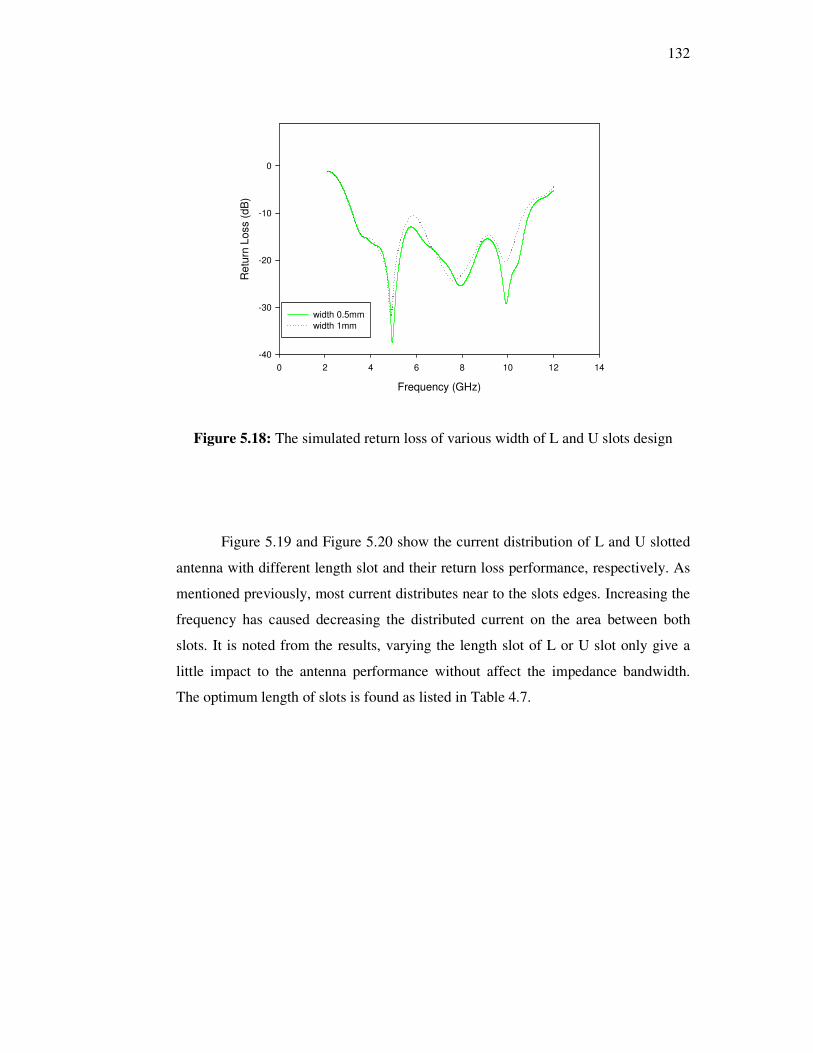
132
Frequency (GHz)
0 2 4 6 8 10 12 14
Re
turn
Lo
ss (
dB
)
-40
-30
-20
-10
0
width 0.5mm
width 1mm
Figure 5.18: The simulated return loss of various width of L and U slots design
Figure 5.19 and Figure 5.20 show the current distribution of L and U slotted
antenna with different length slot and their return loss performance, respectively. As
mentioned previously, most current distributes near to the slots edges. Increasing the
frequency has caused decreasing the distributed current on the area between both
slots. It is noted from the results, varying the length slot of L or U slot only give a
little impact to the antenna performance without affect the impedance bandwidth.
The optimum length of slots is found as listed in Table 4.7.
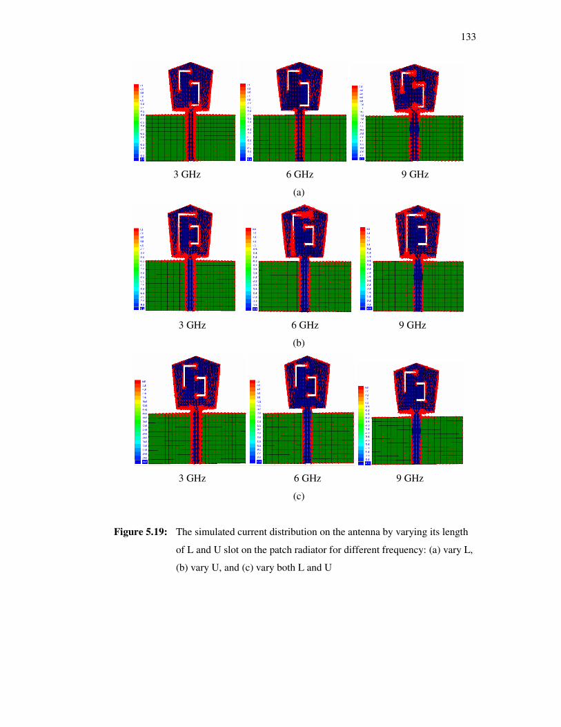
133
3 GHz 6 GHz 9 GHz
(a)
3 GHz 6 GHz 9 GHz
(b)
3 GHz 6 GHz 9 GHz
(c)
Figure 5.19: The simulated current distribution on the antenna by varying its length
of L and U slot on the patch radiator for different frequency: (a) vary L,
(b) vary U, and (c) vary both L and U
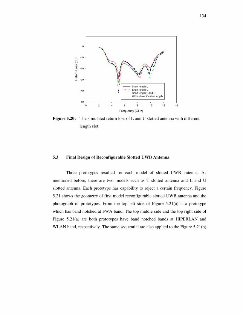
134
Frequency (GHz)
0 2 4 6 8 10 12 14
Re
turn
Lo
ss (
dB
)
-50
-40
-30
-20
-10
0
Short length L
Short length U
Short length L and U
Without modification length
Figure 5.20: The simulated return loss of L and U slotted antenna with different
length slot
5.3 Final Design of Reconfigurable Slotted UWB Antenna
Three prototypes resulted for each model of slotted UWB antenna. As
mentioned before, there are two models such as T slotted antenna and L and U
slotted antenna. Each prototype has capability to reject a certain frequency. Figure
5.21 shows the geometry of first model reconfigurable slotted UWB antenna and the
photograph of prototypes. From the top left side of Figure 5.21(a) is a prototype
which has band notched at FWA band. The top middle side and the top right side of
Figure 5.21(a) are both prototypes have band notched bands at HIPERLAN and
WLAN band, respectively. The same sequential are also applied to the Figure 5.21(b)
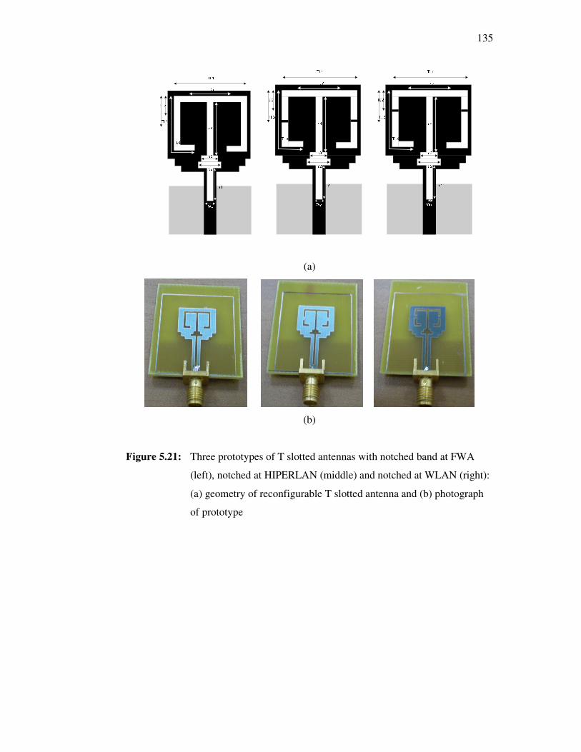
135
(a)
(b)
Figure 5.21: Three prototypes of T slotted antennas with notched band at FWA
(left), notched at HIPERLAN (middle) and notched at WLAN (right):
(a) geometry of reconfigurable T slotted antenna and (b) photograph
of prototype
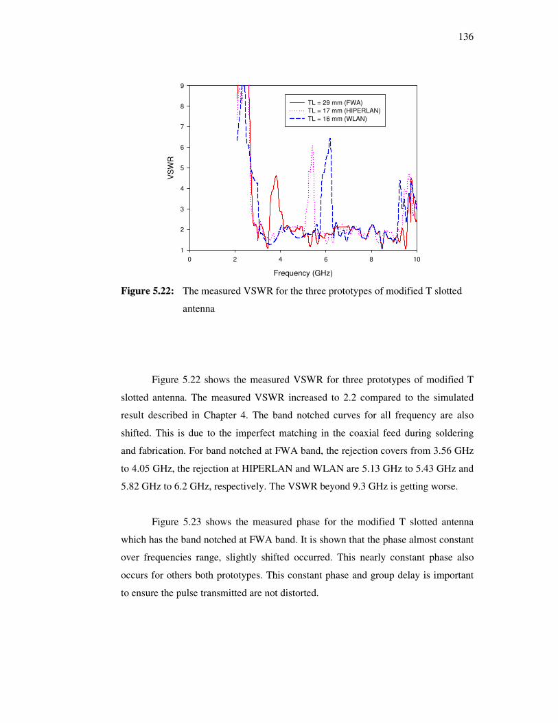
136
Frequency (GHz)
0 2 4 6 8 10
VS
WR
1
2
3
4
5
6
7
8
9
TL = 29 mm (FWA)
TL = 17 mm (HIPERLAN)
TL = 16 mm (WLAN)
Figure 5.22: The measured VSWR for the three prototypes of modified T slotted
antenna
Figure 5.22 shows the measured VSWR for three prototypes of modified T
slotted antenna. The measured VSWR increased to 2.2 compared to the simulated
result described in Chapter 4. The band notched curves for all frequency are also
shifted. This is due to the imperfect matching in the coaxial feed during soldering
and fabrication. For band notched at FWA band, the rejection covers from 3.56 GHz
to 4.05 GHz, the rejection at HIPERLAN and WLAN are 5.13 GHz to 5.43 GHz and
5.82 GHz to 6.2 GHz, respectively. The VSWR beyond 9.3 GHz is getting worse.
Figure 5.23 shows the measured phase for the modified T slotted antenna
which has the band notched at FWA band. It is shown that the phase almost constant
over frequencies range, slightly shifted occurred. This nearly constant phase also
occurs for others both prototypes. This constant phase and group delay is important
to ensure the pulse transmitted are not distorted.
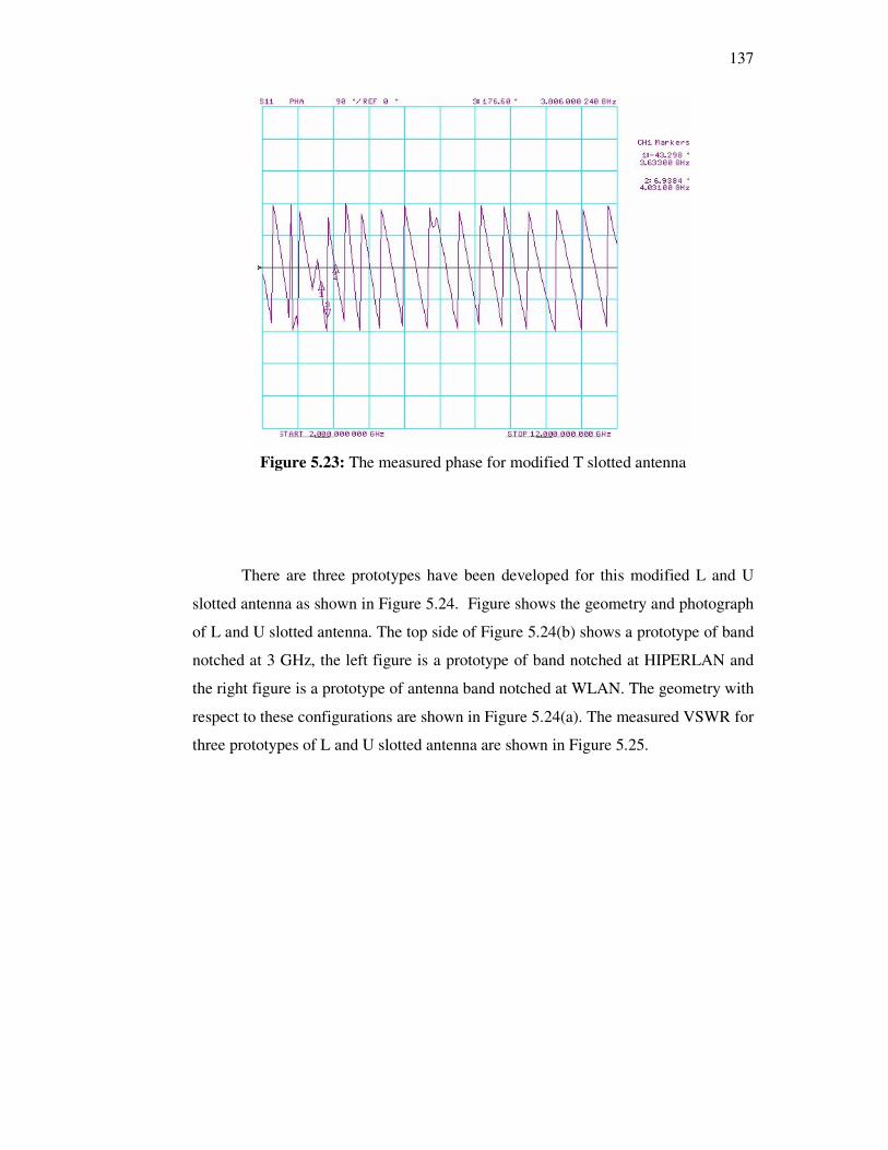
137
Figure 5.23: The measured phase for modified T slotted antenna
There are three prototypes have been developed for this modified L and U
slotted antenna as shown in Figure 5.24. Figure shows the geometry and photograph
of L and U slotted antenna. The top side of Figure 5.24(b) shows a prototype of band
notched at 3 GHz, the left figure is a prototype of band notched at HIPERLAN and
the right figure is a prototype of antenna band notched at WLAN. The geometry with
respect to these configurations are shown in Figure 5.24(a). The measured VSWR for
three prototypes of L and U slotted antenna are shown in Figure 5.25.
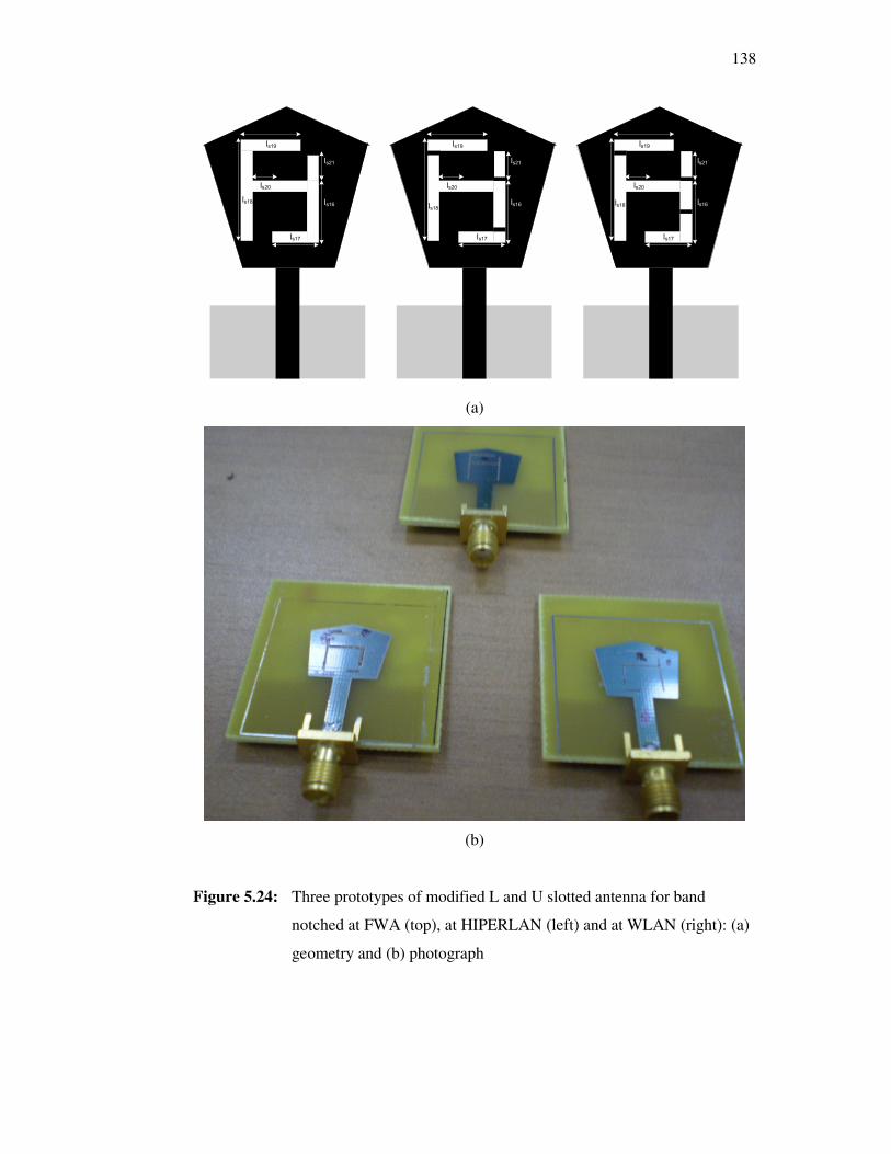
138
ls19
ls18
ls17
ls16
ls20
ls21
ls19
ls18
ls17
ls16
ls20
ls21
ls19
ls18
ls17
ls16
ls20
ls21
(a)
(b)
Figure 5.24: Three prototypes of modified L and U slotted antenna for band
notched at FWA (top), at HIPERLAN (left) and at WLAN (right): (a)
geometry and (b) photograph
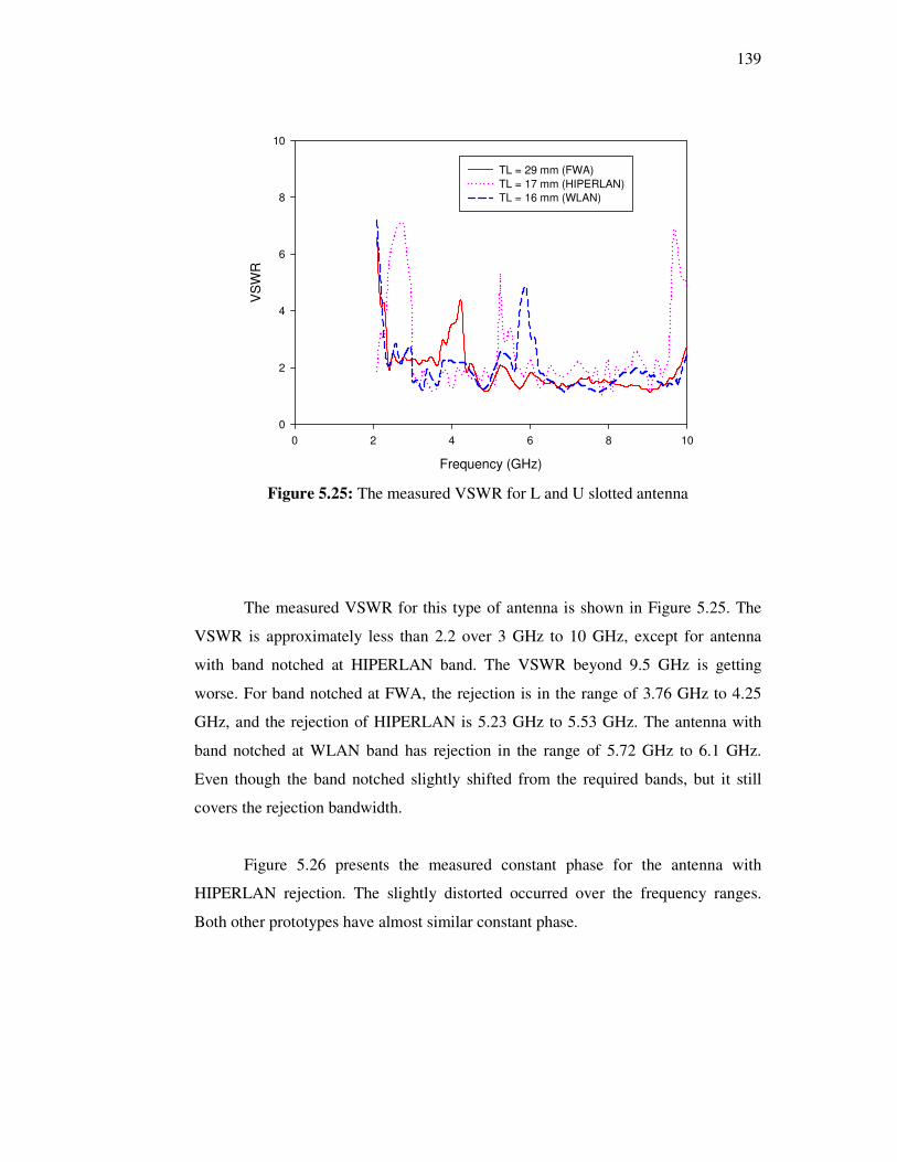
139
Frequency (GHz)
0 2 4 6 8 10
VS
WR
0
2
4
6
8
10
TL = 29 mm (FWA)
TL = 17 mm (HIPERLAN)
TL = 16 mm (WLAN)
Figure 5.25: The measured VSWR for L and U slotted antenna
The measured VSWR for this type of antenna is shown in Figure 5.25. The
VSWR is approximately less than 2.2 over 3 GHz to 10 GHz, except for antenna
with band notched at HIPERLAN band. The VSWR beyond 9.5 GHz is getting
worse. For band notched at FWA, the rejection is in the range of 3.76 GHz to 4.25
GHz, and the rejection of HIPERLAN is 5.23 GHz to 5.53 GHz. The antenna with
band notched at WLAN band has rejection in the range of 5.72 GHz to 6.1 GHz.
Even though the band notched slightly shifted from the required bands, but it still
covers the rejection bandwidth.
Figure 5.26 presents the measured constant phase for the antenna with
HIPERLAN rejection. The slightly distorted occurred over the frequency ranges.
Both other prototypes have almost similar constant phase.
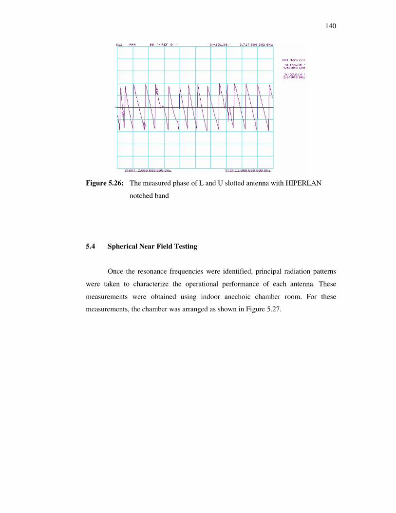
140
Figure 5.26: The measured phase of L and U slotted antenna with HIPERLAN
notched band
5.4 Spherical Near Field Testing
Once the resonance frequencies were identified, principal radiation patterns
were taken to characterize the operational performance of each antenna. These
measurements were obtained using indoor anechoic chamber room. For these
measurements, the chamber was arranged as shown in Figure 5.27.
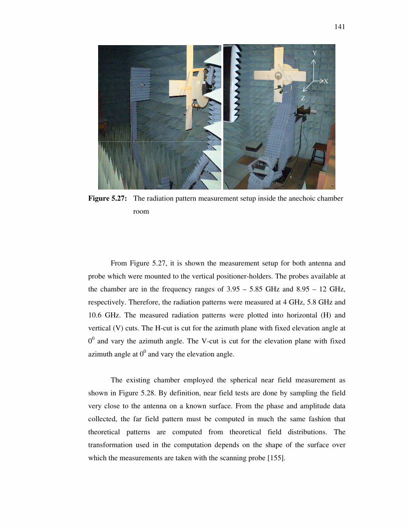
141
Figure 5.27: The radiation pattern measurement setup inside the anechoic chamber
room
From Figure 5.27, it is shown the measurement setup for both antenna and
probe which were mounted to the vertical positioner-holders. The probes available at
the chamber are in the frequency ranges of 3.95 – 5.85 GHz and 8.95 – 12 GHz,
respectively. Therefore, the radiation patterns were measured at 4 GHz, 5.8 GHz and
10.6 GHz. The measured radiation patterns were plotted into horizontal (H) and
vertical (V) cuts. The H-cut is cut for the azimuth plane with fixed elevation angle at
00 and vary the azimuth angle. The V-cut is cut for the elevation plane with fixed
azimuth angle at 00 and vary the elevation angle.
The existing chamber employed the spherical near field measurement as
shown in Figure 5.28. By definition, near field tests are done by sampling the field
very close to the antenna on a known surface. From the phase and amplitude data
collected, the far field pattern must be computed in much the same fashion that
theoretical patterns are computed from theoretical field distributions. The
transformation used in the computation depends on the shape of the surface over
which the measurements are taken with the scanning probe [155].
Y
X
Z
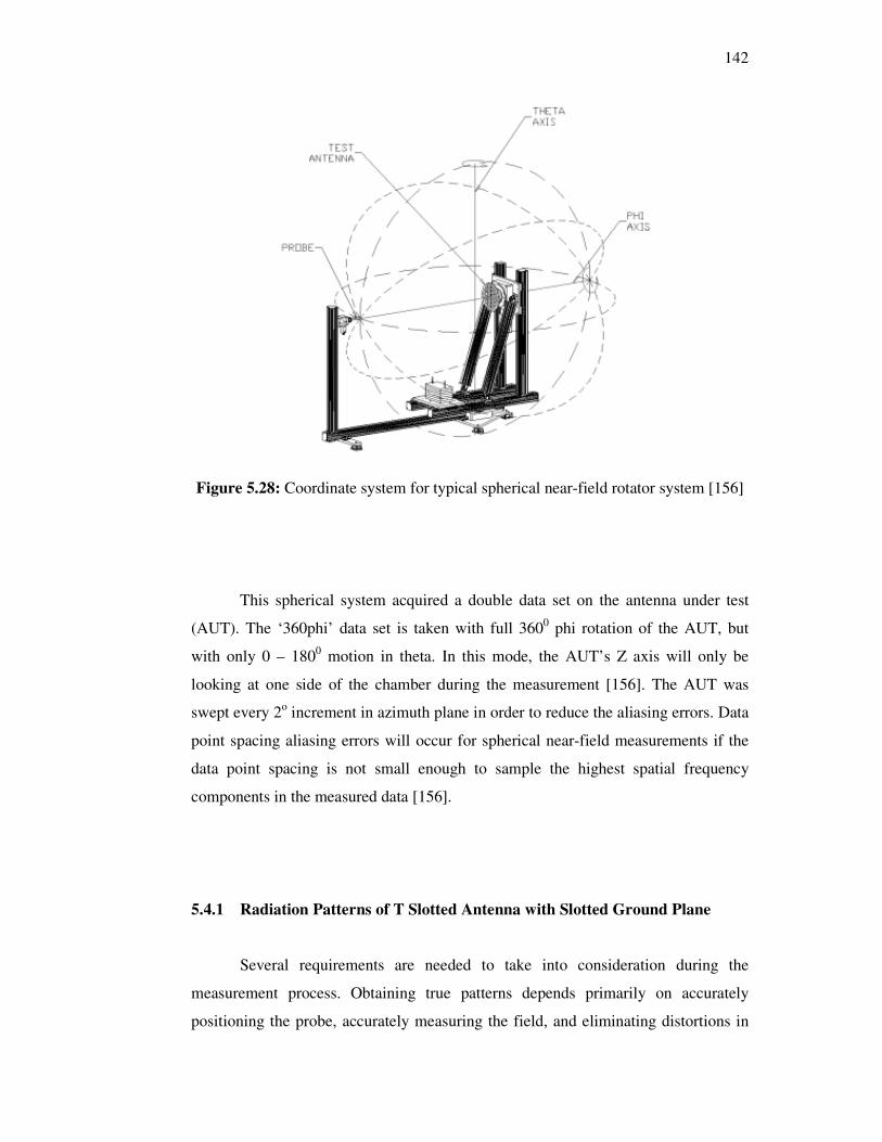
142
Figure 5.28: Coordinate system for typical spherical near-field rotator system [156]
This spherical system acquired a double data set on the antenna under test
(AUT). The ‘360phi’ data set is taken with full 3600 phi rotation of the AUT, but
with only 0 – 1800 motion in theta. In this mode, the AUT’s Z axis will only be
looking at one side of the chamber during the measurement [156]. The AUT was
swept every 2o increment in azimuth plane in order to reduce the aliasing errors. Data
point spacing aliasing errors will occur for spherical near-field measurements if the
data point spacing is not small enough to sample the highest spatial frequency
components in the measured data [156].
5.4.1 Radiation Patterns of T Slotted Antenna with Slotted Ground Plane
Several requirements are needed to take into consideration during the
measurement process. Obtaining true patterns depends primarily on accurately
positioning the probe, accurately measuring the field, and eliminating distortions in
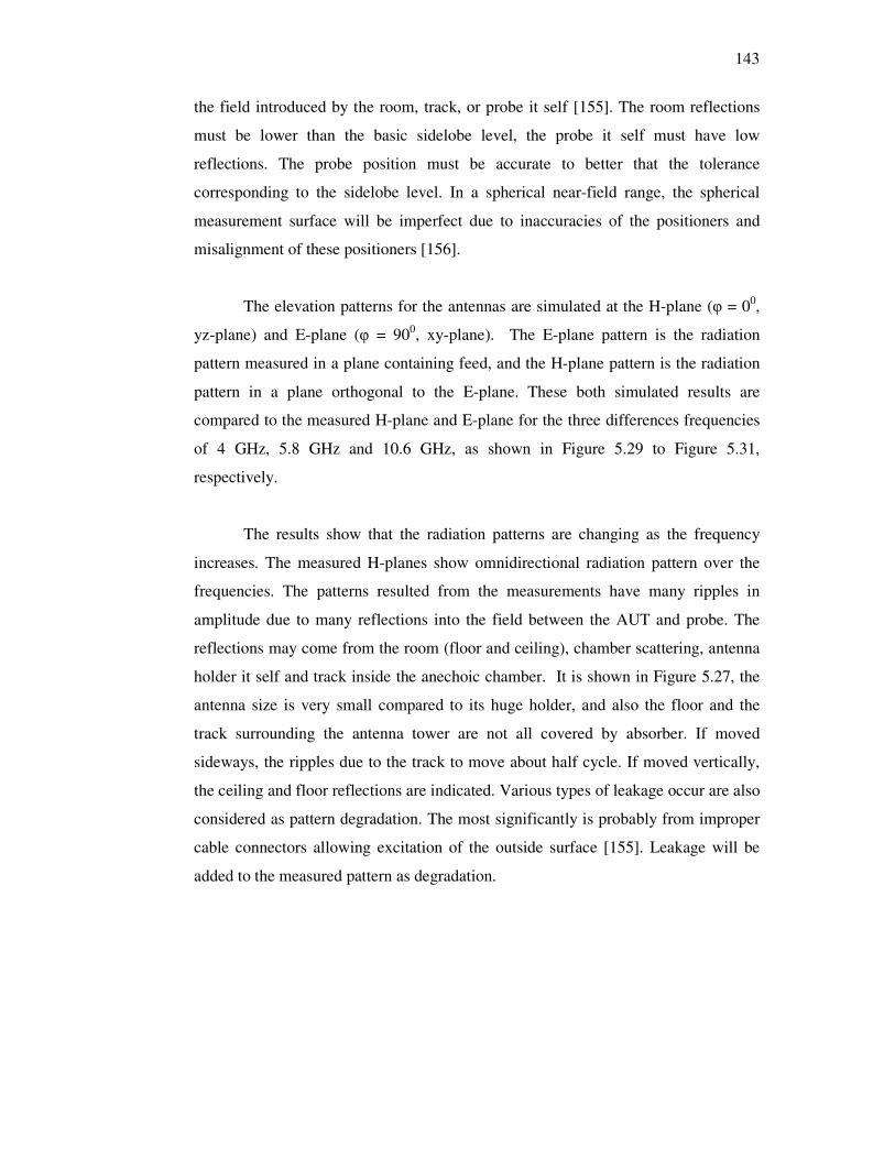
143
the field introduced by the room, track, or probe it self [155]. The room reflections
must be lower than the basic sidelobe level, the probe it self must have low
reflections. The probe position must be accurate to better that the tolerance
corresponding to the sidelobe level. In a spherical near-field range, the spherical
measurement surface will be imperfect due to inaccuracies of the positioners and
misalignment of these positioners [156].
The elevation patterns for the antennas are simulated at the H-plane (φ = 00,
yz-plane) and E-plane (φ = 900, xy-plane). The E-plane pattern is the radiation
pattern measured in a plane containing feed, and the H-plane pattern is the radiation
pattern in a plane orthogonal to the E-plane. These both simulated results are
compared to the measured H-plane and E-plane for the three differences frequencies
of 4 GHz, 5.8 GHz and 10.6 GHz, as shown in Figure 5.29 to Figure 5.31,
respectively.
The results show that the radiation patterns are changing as the frequency
increases. The measured H-planes show omnidirectional radiation pattern over the
frequencies. The patterns resulted from the measurements have many ripples in
amplitude due to many reflections into the field between the AUT and probe. The
reflections may come from the room (floor and ceiling), chamber scattering, antenna
holder it self and track inside the anechoic chamber. It is shown in Figure 5.27, the
antenna size is very small compared to its huge holder, and also the floor and the
track surrounding the antenna tower are not all covered by absorber. If moved
sideways, the ripples due to the track to move about half cycle. If moved vertically,
the ceiling and floor reflections are indicated. Various types of leakage occur are also
considered as pattern degradation. The most significantly is probably from improper
cable connectors allowing excitation of the outside surface [155]. Leakage will be
added to the measured pattern as degradation.
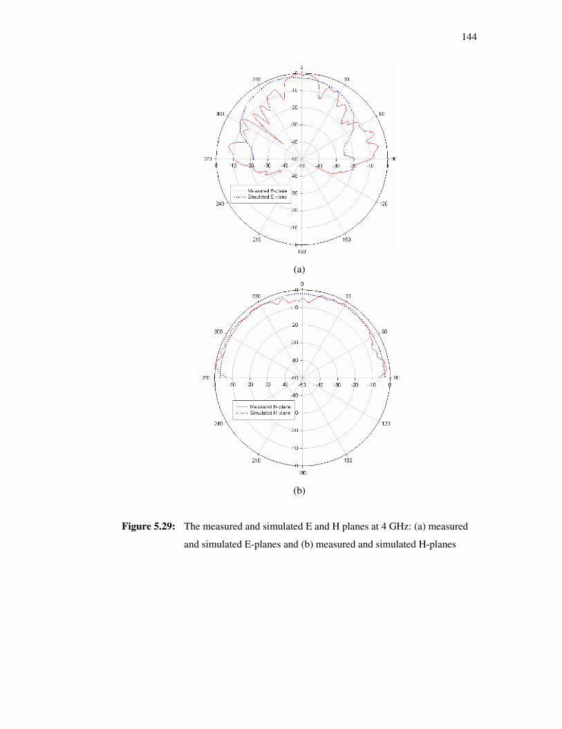
144
(a)
(b)
Figure 5.29: The measured and simulated E and H planes at 4 GHz: (a) measured
and simulated E-planes and (b) measured and simulated H-planes
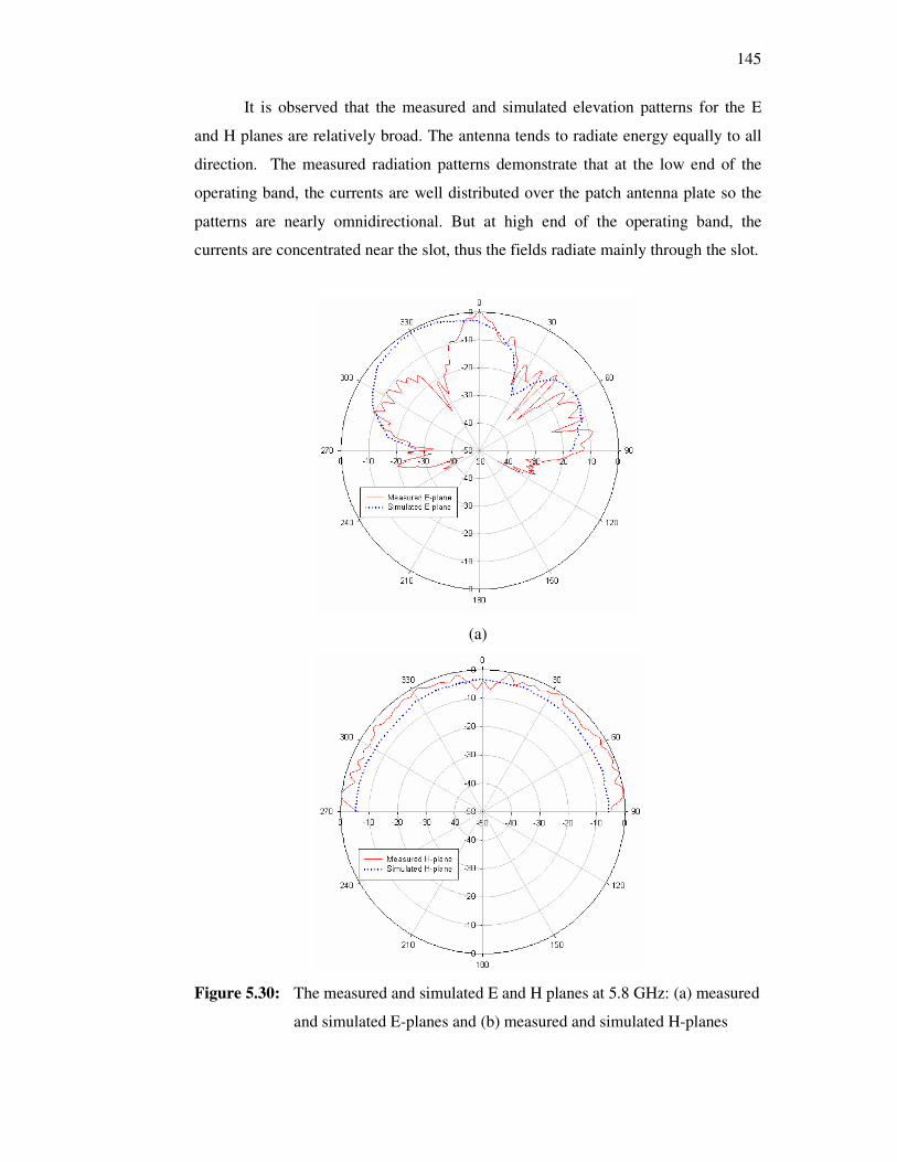
145
It is observed that the measured and simulated elevation patterns for the E
and H planes are relatively broad. The antenna tends to radiate energy equally to all
direction. The measured radiation patterns demonstrate that at the low end of the
operating band, the currents are well distributed over the patch antenna plate so the
patterns are nearly omnidirectional. But at high end of the operating band, the
currents are concentrated near the slot, thus the fields radiate mainly through the slot.
(a)
Figure 5.30: The measured and simulated E and H planes at 5.8 GHz: (a) measured
and simulated E-planes and (b) measured and simulated H-planes
146
It is also noted from Figure 5.30 that with increasing frequency to 5.8 GHz,
the E-plane patterns become smaller. Many ripples occurred in this frequency. The
dips also present for various different angles. Even though the measured radiation
patterns are slightly difference to the simulated ones, since their patterns are nearly
omni directional and their return losses are less than -10 dB, this proposed antenna
meets the UWB requirements.
(a)
(b)
Figure 5.31: The measured and simulated E and H planes at 10.6 GHz: (a)
measured and simulated E-planes and (b) measured and simulated H-
planes
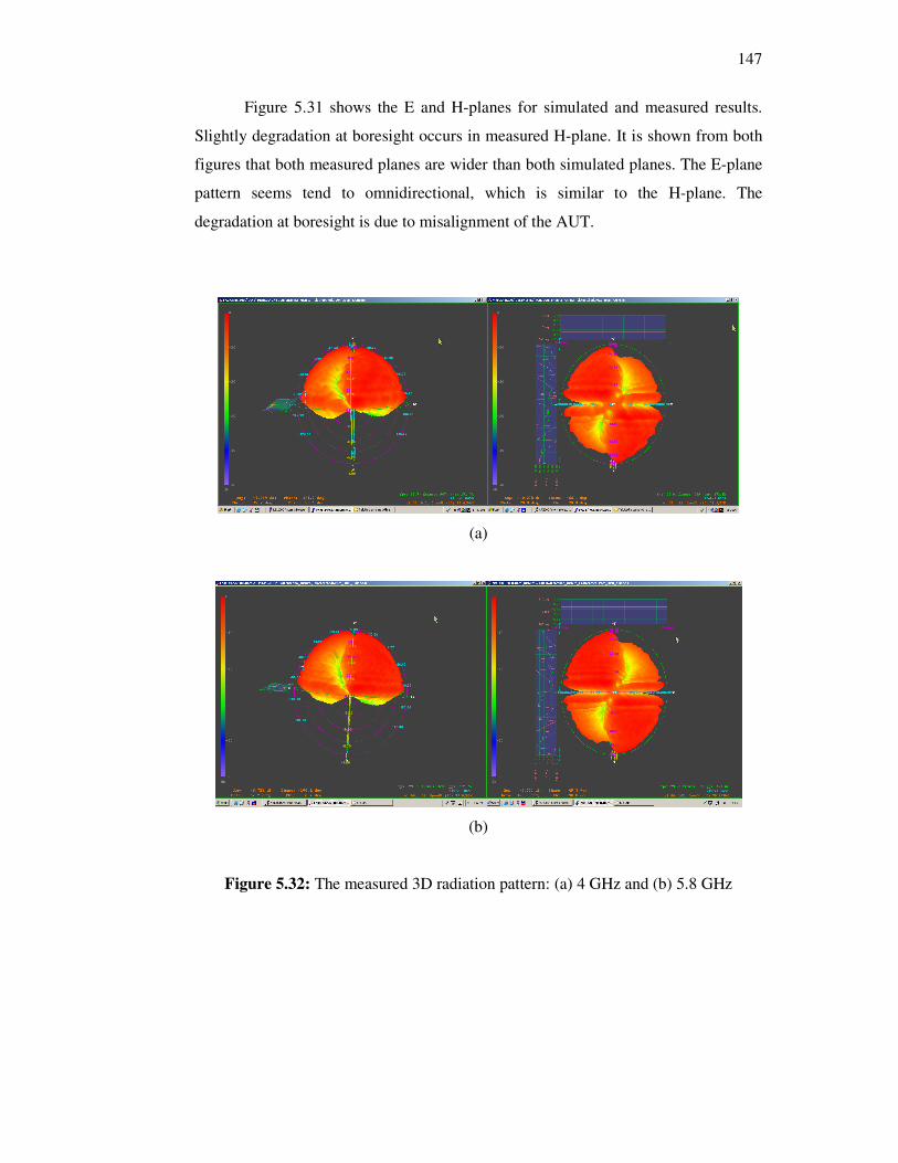
147
Figure 5.31 shows the E and H-planes for simulated and measured results.
Slightly degradation at boresight occurs in measured H-plane. It is shown from both
figures that both measured planes are wider than both simulated planes. The E-plane
pattern seems tend to omnidirectional, which is similar to the H-plane. The
degradation at boresight is due to misalignment of the AUT.
(a)
(b)
Figure 5.32: The measured 3D radiation pattern: (a) 4 GHz and (b) 5.8 GHz
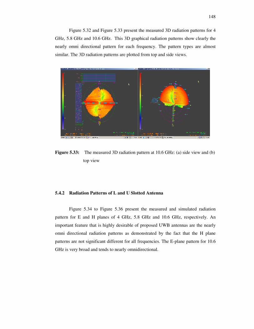
148
Figure 5.32 and Figure 5.33 present the measured 3D radiation patterns for 4
GHz, 5.8 GHz and 10.6 GHz. This 3D graphical radiation patterns show clearly the
nearly omni directional pattern for each frequency. The pattern types are almost
similar. The 3D radiation patterns are plotted from top and side views.
Figure 5.33: The measured 3D radiation pattern at 10.6 GHz: (a) side view and (b)
top view
5.4.2 Radiation Patterns of L and U Slotted Antenna
Figure 5.34 to Figure 5.36 present the measured and simulated radiation
pattern for E and H planes of 4 GHz, 5.8 GHz and 10.6 GHz, respectively. An
important feature that is highly desirable of proposed UWB antennas are the nearly
omni directional radiation patterns as demonstrated by the fact that the H plane
patterns are not significant different for all frequencies. The E-plane pattern for 10.6
GHz is very broad and tends to nearly omnidirectional.
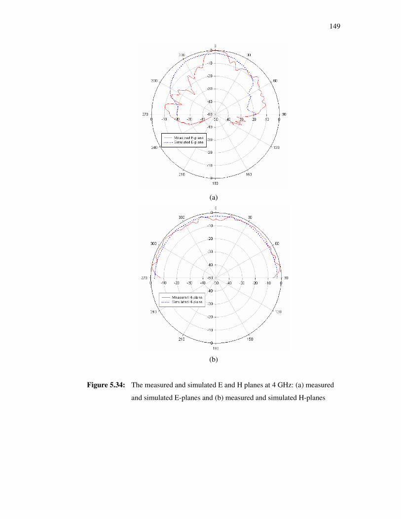
149
(a)
(b)
Figure 5.34: The measured and simulated E and H planes at 4 GHz: (a) measured
and simulated E-planes and (b) measured and simulated H-planes
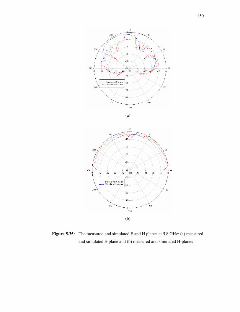
150
(a)
(b)
Figure 5.35: The measured and simulated E and H planes at 5.8 GHz: (a) measured
and simulated E-plane and (b) measured and simulated H-planes
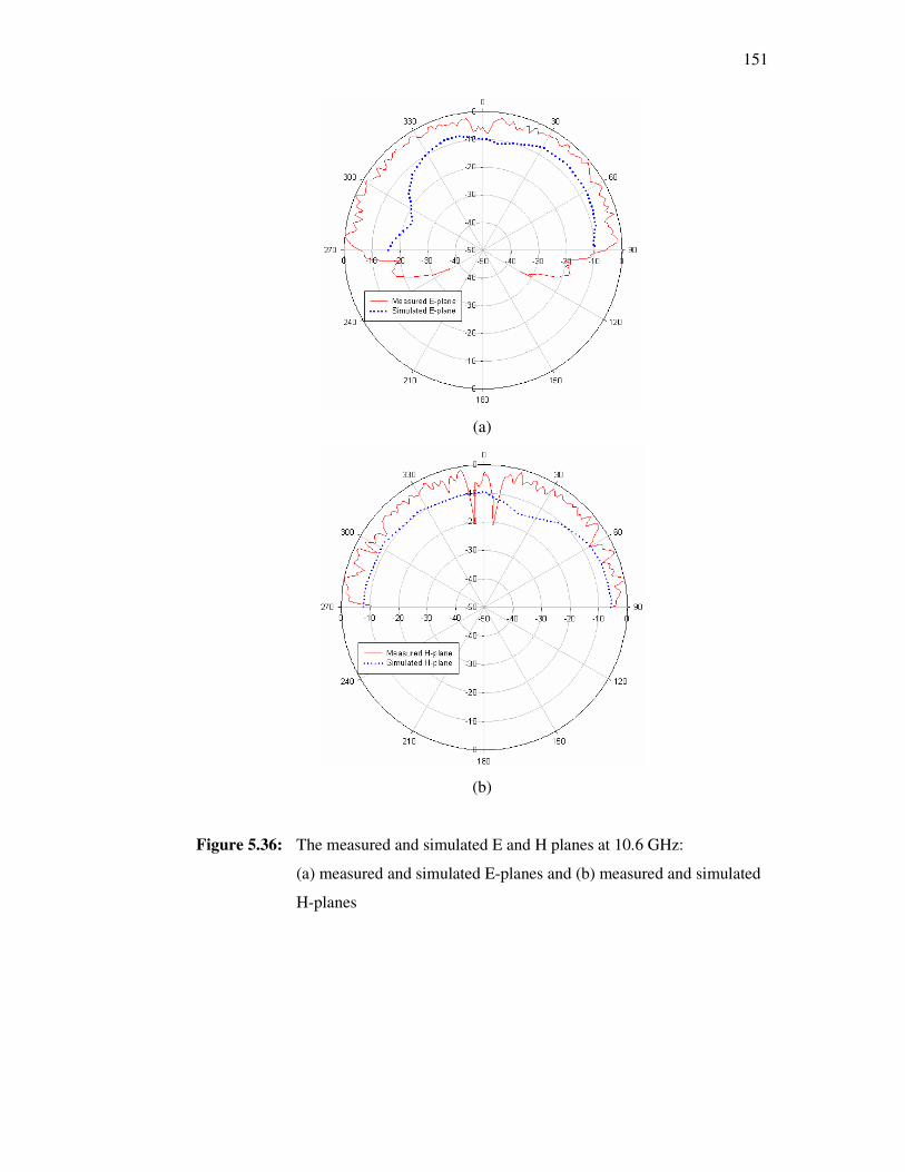
151
(a)
(b)
Figure 5.36: The measured and simulated E and H planes at 10.6 GHz:
(a) measured and simulated E-planes and (b) measured and simulated
H-planes
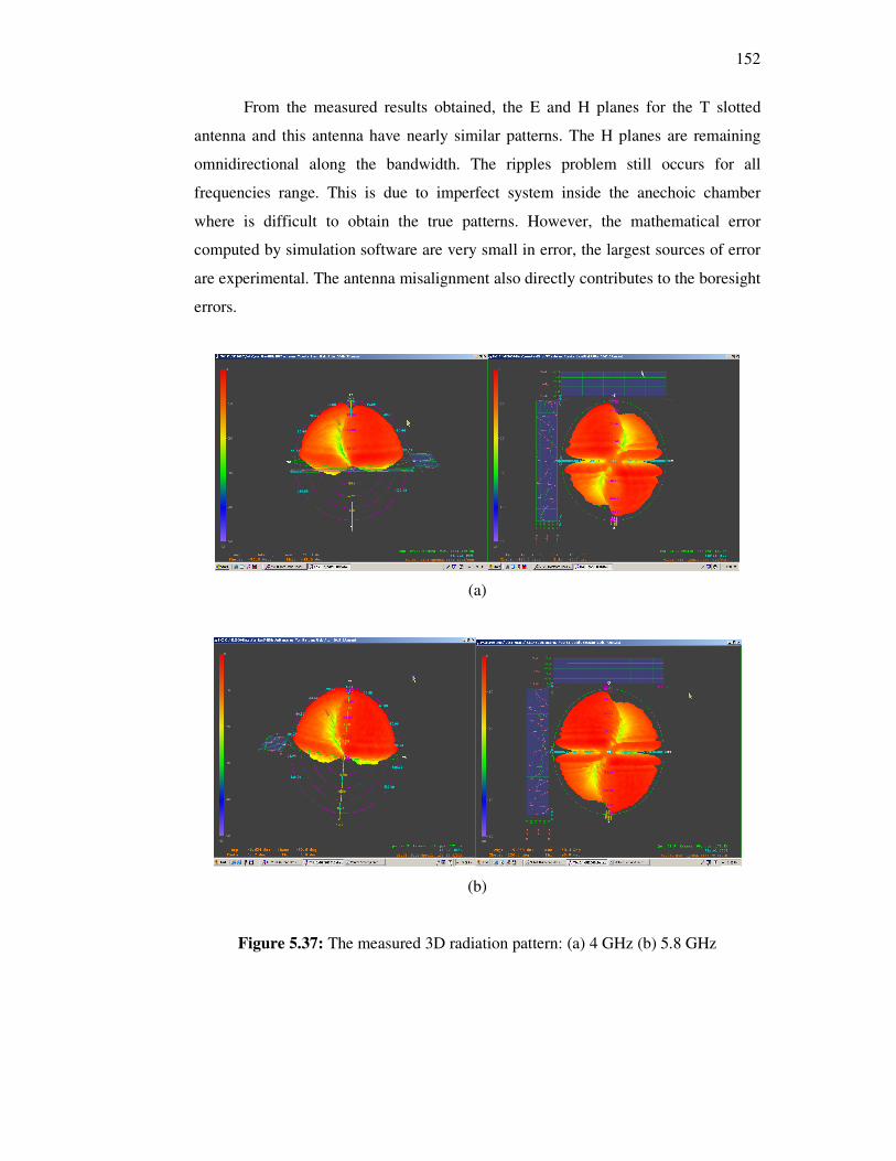
152
From the measured results obtained, the E and H planes for the T slotted
antenna and this antenna have nearly similar patterns. The H planes are remaining
omnidirectional along the bandwidth. The ripples problem still occurs for all
frequencies range. This is due to imperfect system inside the anechoic chamber
where is difficult to obtain the true patterns. However, the mathematical error
computed by simulation software are very small in error, the largest sources of error
are experimental. The antenna misalignment also directly contributes to the boresight
errors.
(a)
(b)
Figure 5.37: The measured 3D radiation pattern: (a) 4 GHz (b) 5.8 GHz
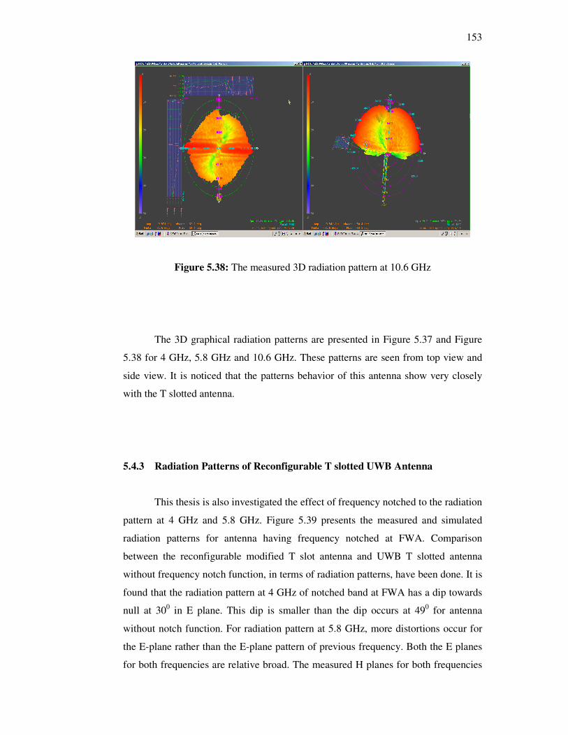
153
Figure 5.38: The measured 3D radiation pattern at 10.6 GHz
The 3D graphical radiation patterns are presented in Figure 5.37 and Figure
5.38 for 4 GHz, 5.8 GHz and 10.6 GHz. These patterns are seen from top view and
side view. It is noticed that the patterns behavior of this antenna show very closely
with the T slotted antenna.
5.4.3 Radiation Patterns of Reconfigurable T slotted UWB Antenna
This thesis is also investigated the effect of frequency notched to the radiation
pattern at 4 GHz and 5.8 GHz. Figure 5.39 presents the measured and simulated
radiation patterns for antenna having frequency notched at FWA. Comparison
between the reconfigurable modified T slot antenna and UWB T slotted antenna
without frequency notch function, in terms of radiation patterns, have been done. It is
found that the radiation pattern at 4 GHz of notched band at FWA has a dip towards
null at 300 in E plane. This dip is smaller than the dip occurs at 49
0 for antenna
without notch function. For radiation pattern at 5.8 GHz, more distortions occur for
the E-plane rather than the E-plane pattern of previous frequency. Both the E planes
for both frequencies are relative broad. The measured H planes for both frequencies
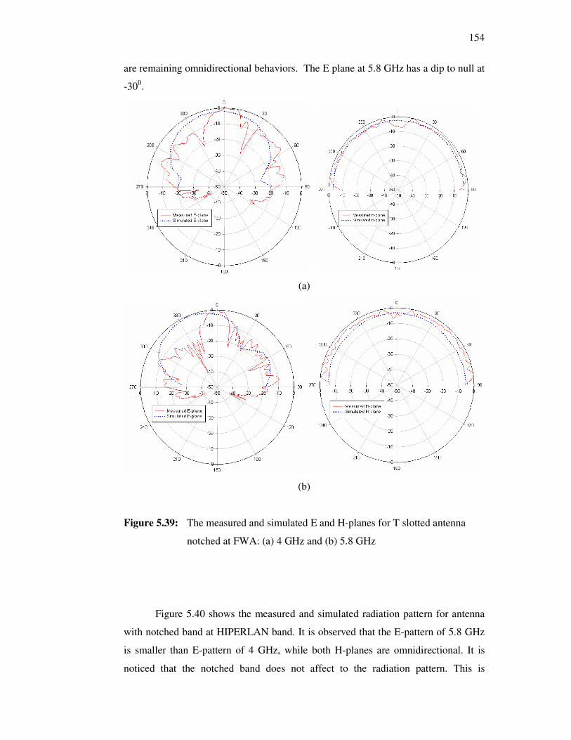
154
are remaining omnidirectional behaviors. The E plane at 5.8 GHz has a dip to null at
-300.
(a)
(b)
Figure 5.39: The measured and simulated E and H-planes for T slotted antenna
notched at FWA: (a) 4 GHz and (b) 5.8 GHz
Figure 5.40 shows the measured and simulated radiation pattern for antenna
with notched band at HIPERLAN band. It is observed that the E-pattern of 5.8 GHz
is smaller than E-pattern of 4 GHz, while both H-planes are omnidirectional. It is
noticed that the notched band does not affect to the radiation pattern. This is
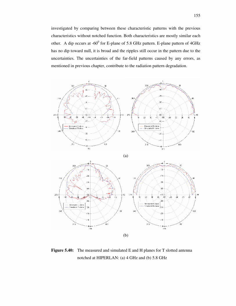
155
investigated by comparing between these characteristic patterns with the previous
characteristics without notched function. Both characteristics are mostly similar each
other. A dip occurs at -600 for E-plane of 5.8 GHz pattern. E-plane pattern of 4GHz
has no dip toward null, it is broad and the ripples still occur in the pattern due to the
uncertainties. The uncertainties of the far-field patterns caused by any errors, as
mentioned in previous chapter, contribute to the radiation pattern degradation.
(a)
(b)
Figure 5.40: The measured and simulated E and H planes for T slotted antenna
notched at HIPERLAN: (a) 4 GHz and (b) 5.8 GHz
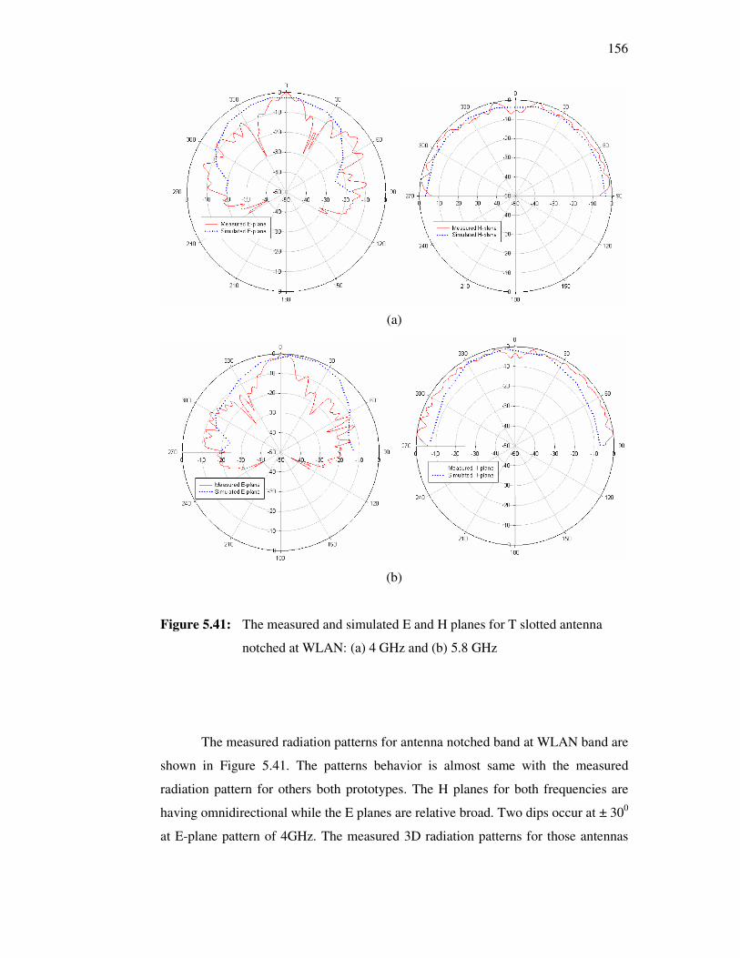
156
(a)
(b)
Figure 5.41: The measured and simulated E and H planes for T slotted antenna
notched at WLAN: (a) 4 GHz and (b) 5.8 GHz
The measured radiation patterns for antenna notched band at WLAN band are
shown in Figure 5.41. The patterns behavior is almost same with the measured
radiation pattern for others both prototypes. The H planes for both frequencies are
having omnidirectional while the E planes are relative broad. Two dips occur at ± 300
at E-plane pattern of 4GHz. The measured 3D radiation patterns for those antennas
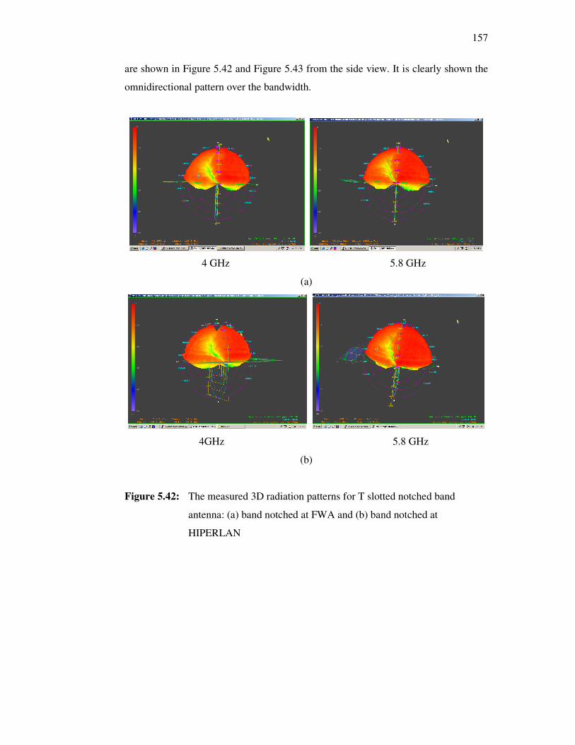
157
are shown in Figure 5.42 and Figure 5.43 from the side view. It is clearly shown the
omnidirectional pattern over the bandwidth.
4 GHz 5.8 GHz
(a)
4GHz 5.8 GHz
(b)
Figure 5.42: The measured 3D radiation patterns for T slotted notched band
antenna: (a) band notched at FWA and (b) band notched at
HIPERLAN
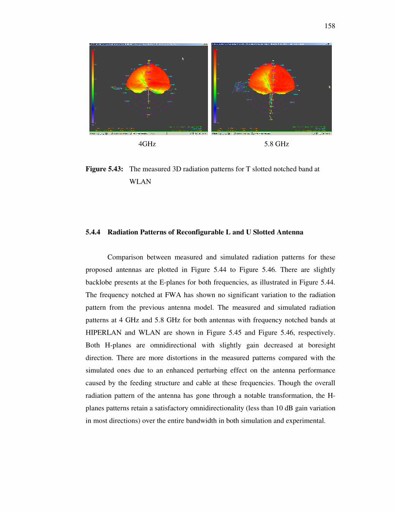
158
4GHz 5.8 GHz
Figure 5.43: The measured 3D radiation patterns for T slotted notched band at
WLAN
5.4.4 Radiation Patterns of Reconfigurable L and U Slotted Antenna
Comparison between measured and simulated radiation patterns for these
proposed antennas are plotted in Figure 5.44 to Figure 5.46. There are slightly
backlobe presents at the E-planes for both frequencies, as illustrated in Figure 5.44.
The frequency notched at FWA has shown no significant variation to the radiation
pattern from the previous antenna model. The measured and simulated radiation
patterns at 4 GHz and 5.8 GHz for both antennas with frequency notched bands at
HIPERLAN and WLAN are shown in Figure 5.45 and Figure 5.46, respectively.
Both H-planes are omnidirectional with slightly gain decreased at boresight
direction. There are more distortions in the measured patterns compared with the
simulated ones due to an enhanced perturbing effect on the antenna performance
caused by the feeding structure and cable at these frequencies. Though the overall
radiation pattern of the antenna has gone through a notable transformation, the H-
planes patterns retain a satisfactory omnidirectionality (less than 10 dB gain variation
in most directions) over the entire bandwidth in both simulation and experimental.
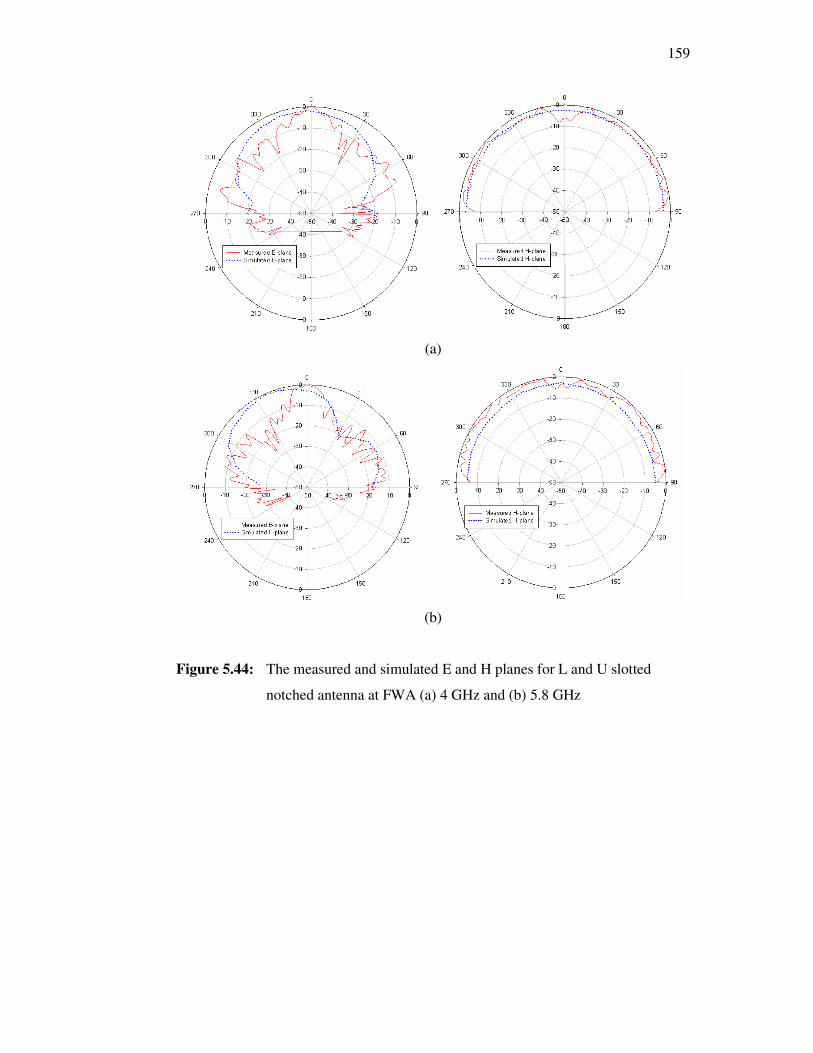
159
(a)
(b)
Figure 5.44: The measured and simulated E and H planes for L and U slotted
notched antenna at FWA (a) 4 GHz and (b) 5.8 GHz
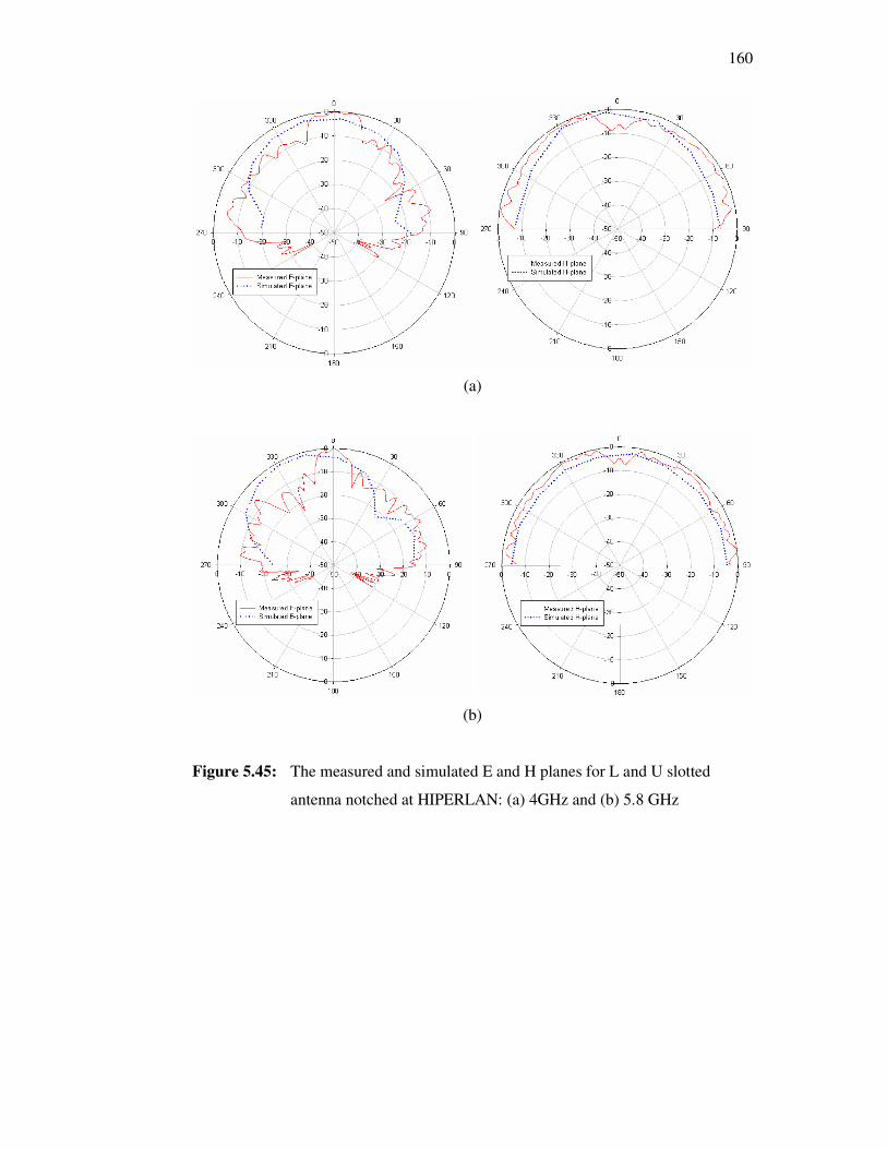
160
(a)
(b)
Figure 5.45: The measured and simulated E and H planes for L and U slotted
antenna notched at HIPERLAN: (a) 4GHz and (b) 5.8 GHz
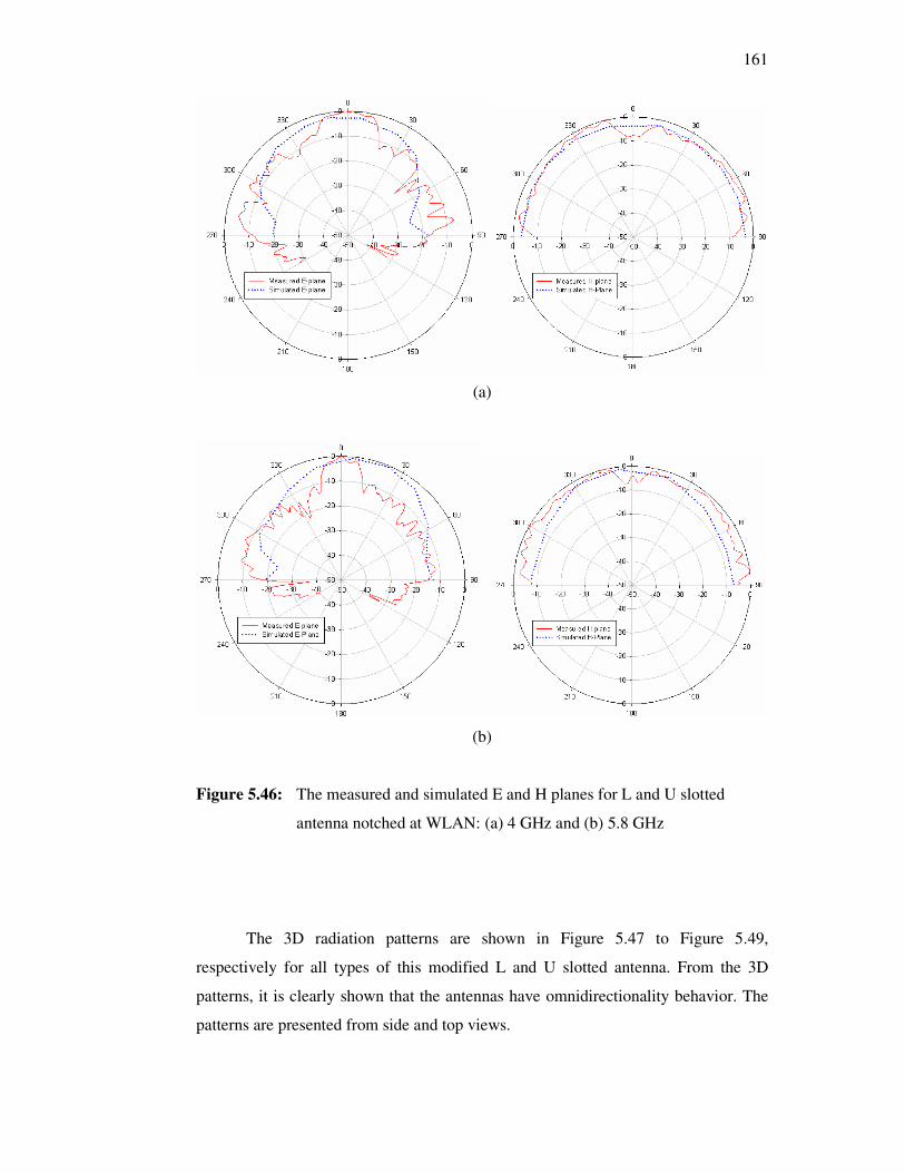
161
(a)
(b)
Figure 5.46: The measured and simulated E and H planes for L and U slotted
antenna notched at WLAN: (a) 4 GHz and (b) 5.8 GHz
The 3D radiation patterns are shown in Figure 5.47 to Figure 5.49,
respectively for all types of this modified L and U slotted antenna. From the 3D
patterns, it is clearly shown that the antennas have omnidirectionality behavior. The
patterns are presented from side and top views.
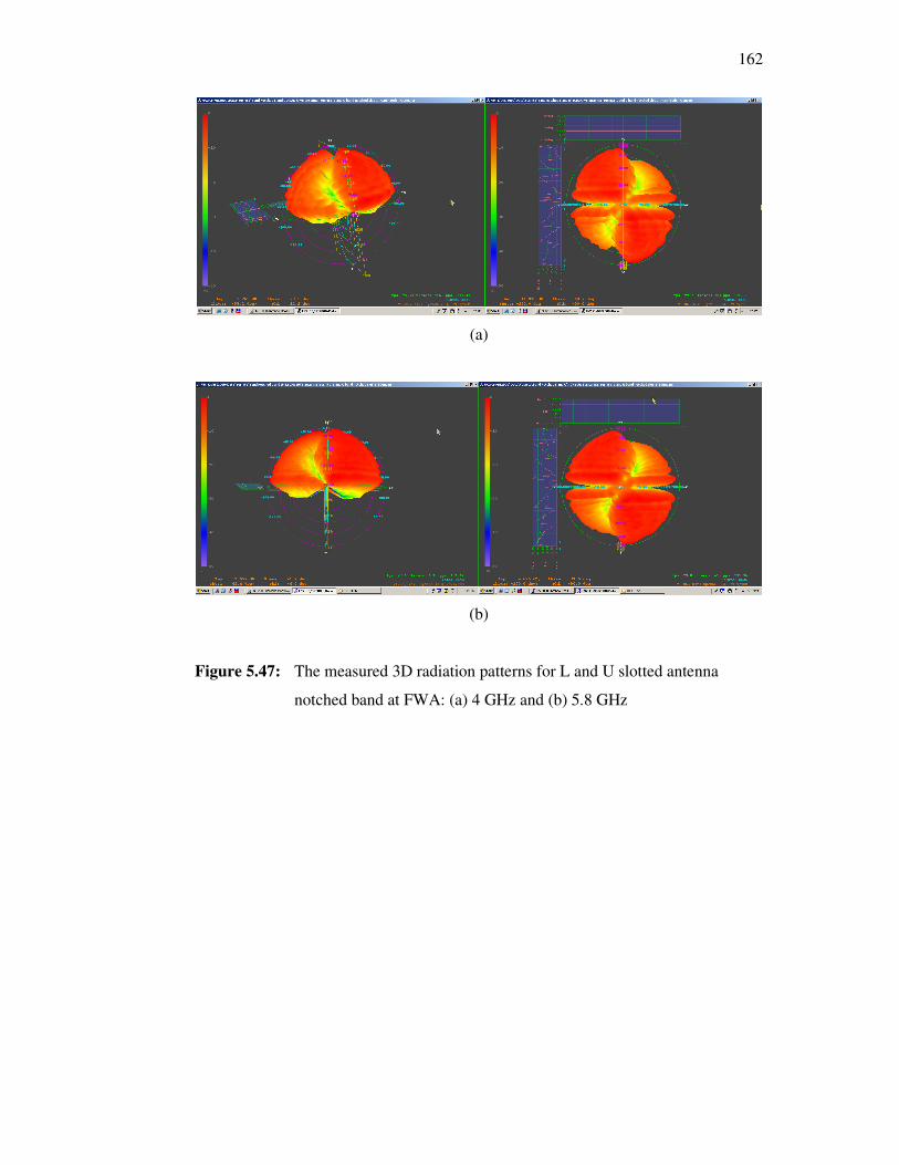
162
(a)
(b)
Figure 5.47: The measured 3D radiation patterns for L and U slotted antenna
notched band at FWA: (a) 4 GHz and (b) 5.8 GHz
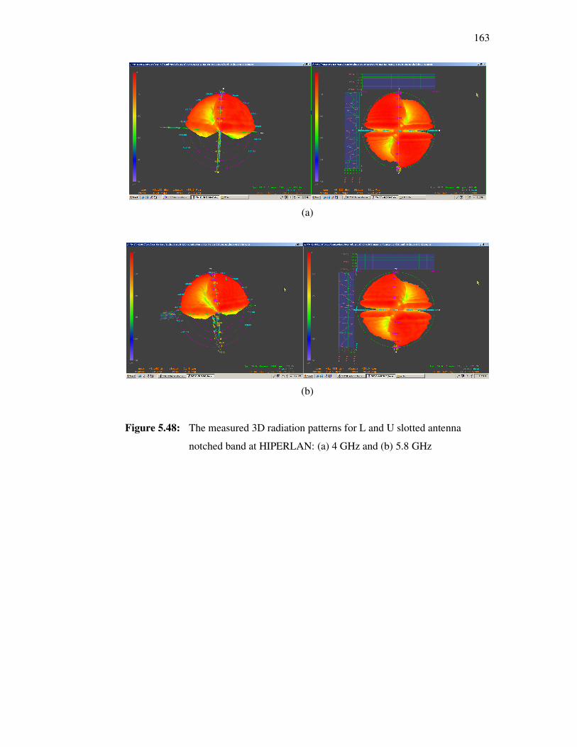
163
(a)
(b)
Figure 5.48: The measured 3D radiation patterns for L and U slotted antenna
notched band at HIPERLAN: (a) 4 GHz and (b) 5.8 GHz
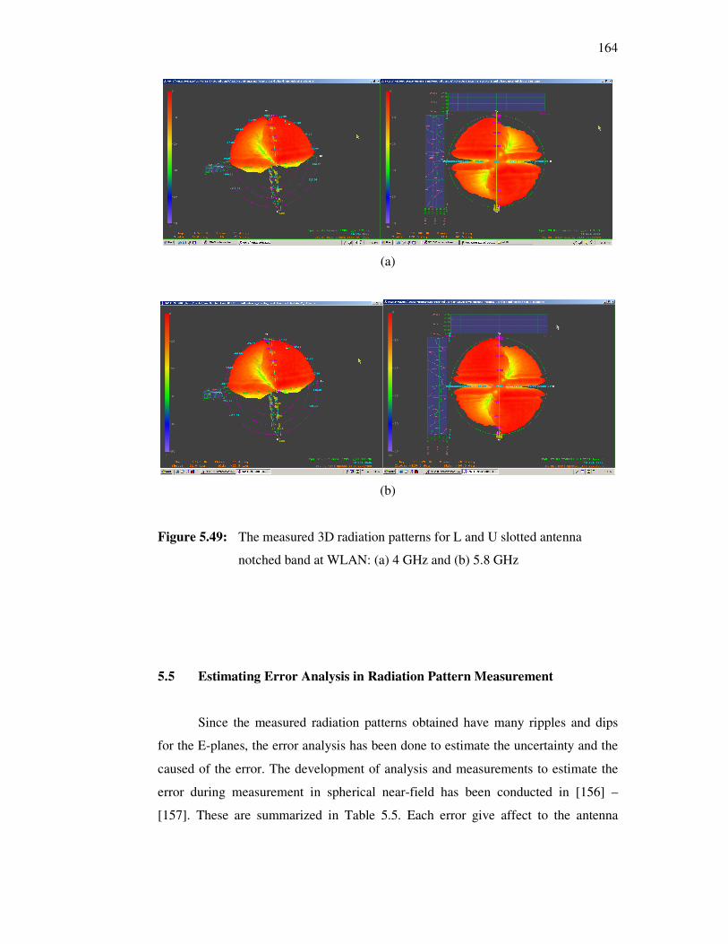
164
(a)
(b)
Figure 5.49: The measured 3D radiation patterns for L and U slotted antenna
notched band at WLAN: (a) 4 GHz and (b) 5.8 GHz
5.5 Estimating Error Analysis in Radiation Pattern Measurement
Since the measured radiation patterns obtained have many ripples and dips
for the E-planes, the error analysis has been done to estimate the uncertainty and the
caused of the error. The development of analysis and measurements to estimate the
error during measurement in spherical near-field has been conducted in [156] –
[157]. These are summarized in Table 5.5. Each error give affect to the antenna
165
performance and some corrections have been taken to ensure the correct results
achieved.
Table 5.5: Near field error analysis for spherical measurement [156] – [157].
No. Error terms Far-field parameters
affected
1 Multiple reflection Gain, side lobe, cross-pol,
pointing
2 AUT alignment Pointing, pattern comparisons
3 Rotator alignment and position errors Gain, side lobe, cross-pol,
pointing
4 Drift correction Gain, pointing
5 Probe rotary joint Gain, side lobe, cross-pol,
pointing
6 Room scattering Gain, side lobe, cross-pol,
pointing
7 Random errors in amplitude/phase Gain, side lobe, cross-pol,
pointing
Table 5.5 lists the possible errors occur during the measurement procedures.
The multiple reflections, rotator alignment, probe rotary joint and room scattering are
shown as primary sources of errors that cause degradation in measured radiation
pattern.
Multiple reflections between the AUT and probe produce the ripple in the
measured data. The correction is difficult to do due to the need a series of near-field
measurements at Z-positions separated by λ/8. The far-fields are then calculated for
each and averaged [126]. In the case of multiple reflections and random errors,
multiple measurements are required.
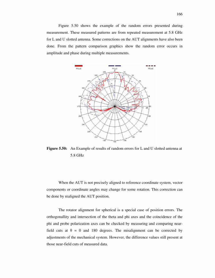
166
Figure 5.50 shows the example of the random errors presented during
measurement. These measured patterns are from repeated measurement at 5.8 GHz
for L and U slotted antenna. Some corrections on the AUT alignments have also been
done. From the pattern comparison graphics show the random error occurs in
amplitude and phase during multiple measurements.
Figure 5.50: An Example of results of random errors for L and U slotted antenna at
5.8 GHz
When the AUT is not precisely aligned to reference coordinate system, vector
components or coordinate angles may change for some rotation. This correction can
be done by realigned the AUT position.
The rotator alignment for spherical is a special case of position errors. The
orthogonallity and intersection of the theta and phi axes and the coincidence of the
phi and probe polarization axes can be checked by measuring and comparing near-
field cuts at θ = 0 and 180 degrees. The misalignment can be corrected by
adjustments of the mechanical system. However, the difference values still present at
those near-field cuts of measured data.
167
The thermal drift during measurements can cause changes in the transmission
lines as well as the alignment of the AUT. It is usually have little effect on the far-
field patterns.
The probe rotary joints associated with the theta and phi rotators produce
some amplitude and phase variations as it is moved and this is as a function of theta
and phi. The error can be observed from the measured data by comparing the
amplitudes and phases of the two components at (θ, φ) coordinates, (0, 0) and (0,180)
[157]. At these points, the amplitude should be identical and the phases should be
either identical or 180 degrees different. This error is more important at high
frequencies where rotary joints may not be as accurate. From the measured data
obtained, it is observed that the variations have presented in amplitudes and phases
for those points of both proposed antennas. Thus, this error contributes to the
uncertainty in far-field results.
Both probe and room scattering can produce higher spatial frequencies in the
data. The smaller data point spacing is needed to avoid the aliasing errors. The room
scattering effect can be more severe when low gain AUT’s are being measured [157].
In this measurement, the 20 data point spacing is used for scanner movement.
Scattering from structures and absorber introduces an error that is difficult to
estimate. This is because the procedure is demanding and time consuming. The AUT
and probe must be translated together in a combination of X, Y and Z movements
while maintaining precise angular alignment. The translations should be at least
multiple wavelengths in dimension and the AUT must be realigned in the new
position. Comparison of the patterns from the two locations provides an estimate of
the room scattering but it is difficult to distinguish from alignment differences,
probe/AUT multiple reflections and system drift [157].
168
5.6 Key contributions
The major contributions in the thesis are detailed below:
Firstly, the mechanism which leads to UWB characteristics were proposed
based on the further insight of the operations of UWB various monopoles with and
without slots. The overlapping of multiple resonances which are evenly and closely
spaced accounts for the UWB characteristics. Various slot types are designed by
studying their current behaviors, with much effect to the impedance bandwidth. In
addition, the UWB antennas designed with novelty slot type has produced a new
structure in antenna type.
Secondly, the miniaturization of vertical type T slotted antenna and L and U
slotted antenna was realized by narrowing the patch and inserting the slots while
retaining the UWB characteristics. The proposed antennas are simple in design, small
in size and easy to manufacture. Their sizes are considerable small compared to the
existing UWB antenna in the reference listed.
Thirdly, printed two UWB antennas with asymmetry slots were proposed.
One is T slotted antenna with slotted ground plane and second is L and U slotted
antenna. Both of them feature small size, ease of fabrication, low profile and
compatibility with printed circuit board. Both of them are fed by a SMA coaxial port.
Fourthly, six printed reconfigurable UWB slotted antenna were realized. The
reconfigurable behaviors on the notched band for each antenna were proposed by
varying the length of slots. All proposed antennas exhibits nearly omnidirectional
radiation patterns and broad bandwidth.
Lastly, the reconfigurable antenna with notched band at FWA band assigned
by MCMC Malaysia is as primary contribution in this type of antenna. This
characteristic is obtained with this small slotted UWB antenna by retaining their
UWB performance. All of these antennas proposed in the thesis can provide ultra
wide bandwidth with nearly omni-directional radiation patterns which make them
very suitable for the future UWB applications.
169
5.7 Summary
This chapter presents the slotted and reconfigurable UWB antenna results
with experimental verifications. Both simulated and experimental results are closely
to each other. Slotted UWB antennas show a good impedance matching covering the
UWB requirements. The reconfigurable characteristic for proposed UWB antennas
has been done by inserting the half-wavelength slot to the patch. These proposed
types of antennas are variation from the previous models. The reconfigurability
behaviors are achieved by shortened or widened the slot. The switching is model as a
small patch of 0.7 mm x 1 mm instead of PIN diodes. It has been demonstrated that
the measured results closely to the simulated results. Event though the rejected band
slightly shifted from the expected one but it still covers the frequency range.
The radiation patterns are also studied for notched band characteristics. It is
found that the notched bands do not give any significant effect to the antenna
radiation performance. The uncertainties due to errors in measurements are also
presented as ripples in the patterns.
The imperfect of the anechoic chamber system cause some ripples occurring
in the measured radiation patterns. This is due to many reflections absorbed from
surrounding. Analysis on possible errors occurred during measurement has been
done. The measured relative gain for slotted UWB antennas are given from the H-
plane plots of measured radiation patterns. The simulated gain and directivity for
both antennas are also presented as well. Thus, these antennas are very promising for
UWB application which is small, compact and has a good performance.
170
CHAPTER 6
CONCLUSIONS AND FUTURE WORKS
6.1 Conclusions
The UWB technology will be the key solution for the future WPAN systems.
This is due to its ability to achieve very high data rate which results from the large
frequency spectrum occupied. Besides, extremely low power emission level will
prevent UWB systems from causing severe interference with other wireless systems.
As the only non-digital part of a UWB system, antenna remains as a particular
challenging topic because there are more stringent requirements for a suitable UWB
antenna compared with a narrowband antenna. Therefore, the antenna design and
analysis for UWB systems were carried out in this thesis.
Rectangular planar monopole antenna is chosen as conventional structure,
this is due to a simple structure, low profile, easy to fabricate and UWB
characteristics with nearly omni-directional radiation patterns. T slotted antenna and
L and U slotted antenna originates from a conventional rectangular monopole by
modifying the bottom patch with beveling and notches. Various antenna
configurations with various forms of notch and bevel have also analyzed in order to
form the novelty structure. Slots insertion and truncation ground plane are added to
further improve the impedance bandwidth.
171
Studies indicate that the UWB characteristic is obtained by proper selection
in the size of notch and bevel and the distance between the bottom patch to the
ground plane. In a broad sense, the ground plane serves as an impedance matching
circuit, and it tunes the input impedance and hence changes the operating bandwidth
when the feed gap is varied. Therefore, it is essential to design a smooth transition
between the feeding line and the antenna for good impedance matching over the
entire operational bandwidth.
Investigations have also been carried out in this thesis to analyze the current
distribution of antennas. The dimension of the antenna also has an impact on the
antenna performance because the current is mainly distributed along the edge on the
antenna. Thus, it will be possible to fix which elements will act on each
characteristic. By varying the edges closed to the feeding point means modifying the
current path on the antenna. In addition, the current distributions along the neutral
zone do not much influence to the antenna performance, due to the current levels are
not too strong. Consequently, antenna with neutral zone slot insertion exhibits the
similar characteristics as its antenna without neutral zone slot, as long as the size and
the position of the neutral zone are precisely determined.
The current distributions on various slots of rectangular with two notches and
pentagonal antennas have investigated in this thesis. It is shown that with increasing
the frequency the current much concentrated along the slot edges. The slot also
appears to introduce a capacitive reactance which counteracts the inductive reactance
of the feed. Thus, the slot wideband behavior is due to the fact that the currents along
the edges of the slot introduce the same resonance frequencies, which, in conjunction
with the resonance of the main patch, produce an overall broadband frequency
response characteristic.
The T slotted antenna with slotted ground plane has shown the return loss
varies from -15 dB to -20 dB. However, during fabrication process, the slightly
shifted impedance bandwidth has occurred. This is due to the antenna with slotted
ground plane need very accuracy in alignment between the slotted ground plane and
patch on both sided of substrate. The distance of patch to the ground plane is also
very small of 0.5 mm, where is this distance as the impedance matching.
172
L and U slotted antenna has performed UWB characteristics with feed gap of
1.5 mm to the ground plane. Adding slotted ground plane to this antenna did not give
any improvement to the bandwidth. Therefore, in this antenna, the slotted ground
plane is out of design consideration. From the measurement results, T slotted antenna
and L and U slotted antenna have shown much closed to the simulated one in terms
of the return loss and radiation patterns. Ripples and dips occur on the patterns are
due to the uncertainties caused by any errors during measurement. However, the
omnidirectional patterns exhibit for the H-planes, and the E-planes are relative broad
over the entire bandwidth. It has been shown that the operating bandwidth meets the
FCC requirements.
Reconfigurable UWB antennas with band notched characteristics have been
investigated. There are three models resulted for each antenna model, T slotted
antenna and L and U slotted antenna. The VSWR, radiation patterns and gain are
evaluated. Three notched bands required are FWA assigned by MCMC, HIPERLAN,
and WLAN. This thesis primary contributes to design and develop UWB antenna
with notched band at FWA assigned by MCMC Malaysia. By modifying the length
of slots, the required notched bands are obtained. The measured radiation patterns
show agree well with the simulated one.
6.2 Future Work
Based on the conclusions drawn and the limitations of the work presented,
future work can be carried out in the following areas:
Firstly, it has been shown that both UWB antennas with asymmetry slots
operate over UWB bandwidth. A more detailed understanding of the current
distribution mode mechanism and the impedance variations caused by the asymmetry
slot could lead to improved design of UWB antennas.
Secondly, further study is also needed for this proposed UWB antenna with
different feeding applied, such as coplanar waveguide (CPW). This is useful for the
173
future antenna design, in order to reduce the error due to misalignment between
patch and ground plane printed on both substrates during fabrication process.
Thirdly, in this thesis, all of the antenna measurements are carried out inside
an anechoic chamber. However, imperfect existing antenna holder and far field
measurement systems have led degradation to the radiation patterns. Because of this
antenna is very small, it needs special handling in measurement procedures to avoid
multiple reflections from other sources.
Fourthly, in the future UWB systems, antenna might be embedded inside a
laptop or other devices. Thus, the devices' effects on the antenna performances need
to be investigated. When the antenna is built on a portable device, the impact from
human body should also be considered.
Fifthly, to ensure the performance of UWB antenna, time domain
measurement needs to be evaluated. This is to evaluate how good this antenna
transmits or received the pulse without any distortion and delay.
Sixthly, UWB systems operate at extremely low power level which limits its
transmission range. In order to enhance the quality of the communication link and
improve channel capacity and range, directional systems with high gain are required
for some applications. Therefore, research on UWB directional antenna and antenna
array could be carried out.
Seventhly, inserting the real PIN diodes into antenna structure need to be
developed to ensure the antennas have the required notched bands. A more studies on
electronic drive circuit and the effect of switching to the electromagnetic waves on
antenna need to be investigated. A programmed microcontroller to control the
current source of PIN diodes is needed in order to randomly on/or state the
switching.
Lastly, gain measurement need to be carried out to complete the overall
performance of UWB antennas.
174
REFERENCES
1. Celine Foong Leng Lew. Inverted Trapezoidal Antenna for Pulsed Application.
B.Eng. Thesis. The University of Queensland; 2003.
2. I. Oppermann, M. Hamalainen and J. Iinatti. UWB Theory and Applications.
John Wiley & Sons Ltd. 2004.
3. Pulse LINK, Inc. http://www.fantasma.net
4. Federal Communications Commission (FCC). Revision of Part 15 of the
Commission's Rules Regarding Ultra-Wideband Transmission Systems. First
Report and Order, ET Docket 98-153, FCC 02-48. April, 2002.
http://www.fcc.gov
5. Zhi Ning Chen et al. Considerations for Source Pulses and Antennas in UWB
Radio Systems. IEEE Transactions on Antennas and Propagation. July, 2004.
Vol. 52(7).
6. Liang Jianxin. Antenna Study and Design for Ultra Wideband Communication
Applications. Ph.D. Thesis. Queen Mary, University of London; 2006.
7. M. A. Peyrot Solis, G. M. Galvan Tejada, and H. Jardon Aguilar. State of the
Art in Ultra-Wideband Antennas. 2nd International Conference on Electrical
and Electronics Engineering (ICEEE) and XI Conference on Electrical
Engineering (CIE 2005). Mexico City, Mexico. September 7-9, 2005. 101 –
105.
8. Kamya, Y.Y., and Ryuji Kohno. Ultra Wideband Antenna. IEEE Radio
Communications. June, 2004.
9. J. F. Zurcher and F. E. Gardiol. Broadband Patch Antenna. Norwood, MA:
Artech House. 1995.
10. R. Garg et al. Microstrip Antenna Design Handbook. Ed. Artech House. 2001.
11. Albert K. Y. Lai et al. A Novel Antenna for Ultra-Wideband Application. IEEE
Transactions on Antennas and Propagation. July, 1992. Vol. 40(7).
175
12. Seok H. Choi et al. A New Ultra-Wideband Antenna for UWB Application.
Microwave and Optical Technology Letters. March 5, 2004. Vol. 40(5).
13. E. Guillanton et al. A New Design Tapered Slot Antenna for Ultra-Wideband
Applications. Microwave Opt. Technol. Lett. 1998. Vol. 19: 286-289.
14. N. P. Agrawall, G. Kumar, and K. P. Ray. Wide-Band Planar Monopole
Antennas. IEEE Transactions on Antennas and Propagation. Feb., 1998. Vol.
46(2): 294-295.
15. Chun Yih Wu, Chia Lun Tang and An Chia Chen. UWB Chip Antenna Design
using LTCC Multilayer Technology for Mobile Applications. Asia Pacific
Microwave Conference (APMC), Dec 4-7, 2005. Suzhou, China. 2005.
16. Zhi Ning Chen et al. Planar Antennas. IEEE Microwave Magazine. December,
2006.
17. T. Yang and W. A. Davis. Planar Half-Disk Antenna Structures for Ultra
Wideband Communications. IEEE Antenna Propagat. Soc. Int. Symp. Dig.
2004. Vol. 3: 2508-2511.
18. S. H. Lee, J. K. Park, and J. N. Lee. A Novel CPW-Fed Ultra Wideband
Antenna Design. Microwave Opt. Technol. Lett. 2005. Vol. 44: 393-396.
19. K. L. Wong, T. C. Tseng, and P. L. Teng. Low Profile Ultra Wideband
Antenna for Mobile Phone Applications, Microwave Opt. Technol. Lett. 2004.
Vol. 43: 7-9.
20. Ian Oppermann. The Role of UWB in 4G, Wireless Personal Communication.
Kluwer Academic Publishers. 2004. 121-133.
21. Haruki Kamiya et al. Evaluation of Interference between MB-OFDM UWB
and WLAN Systems using a GTEM Cell. 2008 Asia-Pacific Symposium on
Electromagnetic Compatibility & 19th
International Zurich Symposium on
Electromagnetic Compatibility. Singapore. May 19-22, 2008. 100 – 103.
22. M. Yamada et al. Evaluation of Electromagnetic Interference between UWB
System and WLAN using GTEM Cell. IEEE International Electromagnetic
Compatibility Symposium. July, 2007.
23. Kenneth C. L. Chan and Yi Huang. A Compact Semi-Circular Disk Dipole
with Notched Band for UWB applications. The Institution of Engineering and
Technology Seminar on Ultra Wideband Systems, Technologies and
Applications. 2006. 226-230.
176
24. Kyungho Chung, Jaemoung Kim, and Jaehoon Choi. Wideband Microstrip-Fed
Monopole Antenna Having Frequency Band Notch Function. IEEE Microwave
and Wireless Components Letters. November, 2005. Vol. 15(11).
25. H. G. Schant, G. Wolenec, and E. M. Myszka. Frequency Notched UWB
Antenna. Proc. IEEE Conference on Ultra Wideband Sys and Tech. 2003. 214-
218.
26. Y. Kim and D. H. Kwon. CPW-Fed Planar Ultra-Wideband Antenna Having a
Frequency Band Notch Function. Electronics Letters. April, 2004. Vol. 40(7):
403-405.
27. S. W. Su, K. L. Wong, and F. S. Chang. Compact Printed Ultra-Wideband Slot
Antenna with a Band Notched Operation. Microwave & Optical Techni.
Letters. April, 2005. Vol. 45(2): 128-130.
28. W. Choi et al. Compact Ultra-Wideband Printed Antenna with Band Rejection
Characteristics. Electronics Letters. September, 2005. Vol. 41(18): 990-991.
29. Yongjin Kim, and Do Hoon Kwon. Planar Ultra Wideband Slot Antenna with
Frequency Band Notch Function, Antennas and Propagation Society
International Symposium. IEEE. 2004.
30. H. Yoon et al. A Study of the UWB Antenna with Band Rejection
Characteristic. Proc. IEEE APS Int. Symp. June, 2004. 1784-1787.
31. S. Y. Suh et al. A UWB Antenna with a Stop-Band Notch in the 5 GHz WLAN
Band. Proc. IEEE/ACES International Conference. April, 2005. 203-207.
32. W. J. Lui et al. Frequency Notched Ultra-Wideband Microstrip Slot Antenna
with Fractal Tuning Stub. Electronics Letters. March, 2005. Vol. 41(6): 294-
296.
33. K. H. Kim et al. Band-Notched UWB Planar Monopole Antenna with Two
Parasitic Patches. Electronics Letters. July, 2005. Vol. 41(14): 783-785.
34. W. J. Lui, C. H. Cheng, and H. B. Zhu. Frequency Notched Printed Slot
Antenna with Parasitic Open-Circuit Stub. Electronics Letters. September,
2005. Vol. 41(20): 1094-1095.
35. Zhi Ning Chen, Terence S. P. See, and Xianming Qing. Small Ground-
Independent Planar UWB Antenna. Antennas and Propagation Society
International Symposium 2006. IEEE. 2006.1635-1638.
36. N. Askar. Overview of General Atomics PHY Proposal to the IEEE 802.15.3a.
IEEE P 802.15. March, 2003.
177
37. R. J. Fontana. Recent System Applications of Short-Pulse UWB Technology.
IEEE Transactions on Microwave Theory and Techniques. September, 2004.
Vol. 52(9): 2087-2104.
38. R. J. Fontana. A Brief History of UWB Communications. Multispectral
Solutions Inc. Kluwer Academic/Plenum Publishers. 2000.
http://www.multispectral.com/history.html
39. Harmuth, H. F. Transmission of Information by Orthogonal Functions. 2nd. ed.
New York: Springer. 1969.
40. Harmuth, H. F. Transmission of Information by Orthogonal Functions, 3rd. ed.
New York: Springer. 1972.
41. Harmuth, H. F. Range-Doppler Resolution of Electromagnetic Walsh Waves in
Radar. IEEE Transactions on Electromagnetic Compatibility. EMC-17.1975.
106-111.
42. Harmuth, H. F. Selective Reception of Periodic Electromagnetic Waves With
General Time Variation. IEEE Transactions on Electromagnetic Compatibility.
EMC-19. 1977. 137-144.
43. Harmuth, H. F. Sequency Theory. New York: Academic Press. 1977.
44. Harmuth, H. F. Nonsinusoidal Waves for Radar and Radio Communication.
New York: Academic Press. 1981.
45. Harmuth, H. F. Antennas and Waveguides for Nonsinusoidal Waves. New
York: Academic Press. 1984.
46. Robbins, K.W. Short Baseband Pulse Receiver. U. S. Patent 3,662,316. May 9,
1972.
47. Robbins, K.W., and Robbins, G. F. Stable Baseband Super Regenerative
Selective Receiver. U. S. Patent 3,794,996. Feb. 26, 1974.
48. Ross, G. F. Transmission and Reception System for Generating and Receiving
Baseband Duration Pulse Signals for Short Baseband Pulse Communication
System. U. S. Patent 3,728,632. Apr. 17, 1973.
49. Ross, G. F. Energy Amplifying Selector Gate for Baseband Signals. U. S.
Patent 3,750,025. July 31, 1973.
50. Ross, G. F., and Lamensdorf, D. Balanced Radiator System. U. S. Patent
3,659,203. Apr. 25, 1972.
51. Ross, G. F., and Mara, R. M. Coherent Processing Tunnel Diode Ultra
Wideband Receiver. U. S. Patent 5,337,054. Aug. 9, 1994.
178
52. Ross, G. F., and Robbins, K.W. Baseband Radiation and Reception System.
U. S. Patent 3,739,392. June 12, 1973.
53. Ross, G. F., and Robbins, K.W. Narrow Range-Gate Baseband Receiver. U. S.
Patent 4,695,752. Sep. 22, 1987.
54. Morey, R. N. Geophysical Survey System Employing Electromagnetic Impulse.
U. S. Patent 3,806,795. April, 1974.
55. Kazimierz Siwiak and Debra Mc. Keown. Ultra-Wideband Radio Technology.
John Wiley & Sons, Ltd. 2004.
56. Domenico Porcino. UWB Regulations & Coexistence: From the FCC First
Report and Order to the Path to Approval in Europe. Tutorial at International
Workshop on Ultra Wideband Systems. June, 2003. Oulu, Finland. 2003.
57. European Telecommunications Standards Institute (ETSI). Technical Report,
Technical Characteristics for Short Range Devices Communication Equipment
using Ultra-Wideband Technology. TR 101 994-1, V1.0.0. August, 2003.
58. Hailiang Mei. Modeling and Performance Evaluation of a BPPM UWB System.
Msc. Thesis. Delf University of Technology; July 2003.
59. Nicholas Cravotta. Ultrawideband: The Next Wireless Panacea. October 17,
2002. EDN. www.edn.com
60. Electronic Communications Committee (ECC) Report 64. The Protection
Requirements of Radio Communications Systems below 10.6 GHz from Generic
UWB Applications. February, 2005.
61. William Webb. Ultra Wideband-The Final Few Regulatory Processes. 2006
IET Seminar on Ultra Wideband Systems, Technologies and Applications.
London, U. K. April, 2006.
62. Ryuji Kohno and Kenichi Takizawa. Overview of Research and Development
Activities in NICT UWB Consortium. 2005 IEEE International Conference on
Ultra-Wideband. Zurich, Switzerland. September 5-8, 2005. 735-740.
63. Hans Gregory Schantz. A Brief History of UWB Antennas. IEEE Aerospace
and Electonics System Magazine. Vol; 19 (4): 22-26. April, 2004.
64. Alexander Vorobyov. Planar Elliptically Shaped Dipole Antenna for UWB
Impulse Radio. Ph.D. Thesis. Delf Technical University, Netherlands; 2008.
65. P. S. Carter. Short Wave Antenna. U. S Patent 2,175,252. October 10, 1939.
66. P. S. Carter. Wide Band, Short Wave Antenna and Transmission Line System.
U. S Patent 2,181,870. December 5, 1939.
179
67. Stratton and Chu. Journal of Applied Physics. March, 1941.
68. S. Ramo and J. R. Whinnery. Fields and Waves in Modern Radio. New York.
1944. 480-482.
69. W. L. Stutzman and G. A. Thiele. Antenna and Theory and Design. 2nd. ed.
New York: John Wiley & Sons. 1998.
70. Schelkunoff. Electromagnetic Waves. Van Nostrand, 1943.
71. Johnna Powel. Antenna Design for Ultra wideband Radio. MSc Thesis. Massachusetts Institute of Technology (M. I. T); May 7, 2004.
72. V. H. Rumsey. Frequency Independent Antennas. 1957 IRE National
Convention. 1957.
73. J. D. Dyson. The Equiangular Spiral Antenna. IRE Transactions on Antennas &
Propagations. April, 1959. Vol. AP-7: 181-187.
74. M. Kanda. Transients in a Resistively Loaded Linear Antennas Compared with
those in a Conical Antenna and a TEM Horn. IEEE Transactions on Antennas
and Propagations. Jan, 1980. Vol. 28(1): 132–136.
75. K. L. Shlager, G. S. Smith, and J. G. Maloney. Accurate Analysis of TEM
Horn Antennas for Pulse Radiation. IEEE Trans. Electromagn. Compat. Aug.,
1996. Vol. 38(3): 414–423.
76. B. Scheers, M. Acheroy, and A. Vander Vorst. Time-Domain Simulation and
Characterisation of TEM Horns using a Normalised Impulse Response. Proc.
Inst. Elect. Eng. Microw. Antennas Propagat. Dec., 2000. Vol. 147(6): 463–
468.
77. L. T. Chang and W. D. Burnside. An Ultrawide-Bandwidth Tapered Resistive
TEM Horn Antenna. IEEE Trans. Antennas Propagat. Dec., 2000. Vol. 48(12):
1848–1857.
78. Jennifer T. Bernhard. Reconfigurable Antenna. Morgan & Claypool Publisher.
2007.
79. R. T. Lee and G. S. Smith. On The Characteristic Impedance of the TEM Horn
Antenna. IEEE Trans. Antennas Propagat. Jan., 2004. Vol. 52(1): 315–318.
80. P. E. Mayes. Frequency-Independent Antennas and Broad-band Derivatives
thereof. Proceeding of The IEEE. Jan., 1992. Vol. 80(1): 103–112.
81. T. W. Hertel and G. S. Smith. On the Dispersive Properties of the Conical
Spiral Antenna and Its Use for Pulsed Radiation. IEEE Trans. Antennas
Propagat. July, 2003. Vol. 51(7): 1426–1433.
180
82. T. T. Wu and R.W. P. King. The Cylindrical Antenna with Non-Reflecting
Resistive Loading. IEEE Trans. Antennas Propagat. May, 1965. Vol. 13(3):
369–373.
83. D. L. Senguta and Y. P. Liu. Analytical Investigation of Waveforms Radiated
by a Resistively Loaded Linear Antenna Excited by a Gaussian Pulse. Radio
Sci. June, 1974. Vol. 9(3): 621–630.
84. J. G. Maloney and G. S. Smith. A Study of Transient Radiation from the Wu-
King Resistive Monopole-FDTD Analysis and Experimental Measurements.
IEEE Trans. Antennas Propagat. May, 1993. Vol. 41(5): 668–676.
85. R. H. Duhamel. Dual Polarized Sinuous Antennas. U. S. Patent 4,658,262.
April 14, 1987.
86. S. Honda et al. A Disc Monopole Antenna with 1:8 Impedance Bandwidth and
Omni-Directional Radiation Pattern. Proceedings of the 1992 ISAP. September
1992. Sapporo, Japan. 1992. 1145-1148.
87. P. P. Hammoud and F. Colomel. Matching the Input Impedance of a Broadband
Disc Monopole. Electronics Letters. Feb., 1993. Vol. 29: 406-407.
88. J. A. Evans and M. J. Ammann. Planar Trapezoidal and Pentagonal Monopoles
with Impedance Bandwidth in Excess of 10:1. IEEE International Symposium
Digest. 1999. Orlando. Vol. 3: 1558-1559.
89. R. M. Taylor. A broadband Omni-Directional Antenna. IEEE Antennas and
Propagation Society International Symposium Digest. June, 1994. Vol. 2:
1294–1297.
90. Anatoliy Boryssenko. Time Domain Studies of Ultra Wideband Antennas.
Proceedings of the 1999 IEEE Canadian Conference on Electrical and
Computer Engineering. May 9-12, 1999. Shaw Conference Center, Edmonton,
Alberta, Canada. IEEE. 1999.
91. J. R. Nealy. Foursquare Antenna Radiating Element. U. S. Patent 5,926,137.
July 20, 1999. VTIP Ref. 96-056. http://www.vtip.org
92. Randall Nealy et al. Improvements to the Foursquare Radiating Element-
Trimmed Foursquare. U. S. Patent 6,057,802. May 2, 2000. VTIP Ref. 98-001.
http://www.vtip.org
93. M. Z. Win and R. A. Scholtz. Impulse Radio: How It Works. IEEE Comm.
Letters. January, 1998. Vol. 2(1): 36-38.
181
94. J. Joe. Cellonics UWB Pulse Generators. International Workshop on Ultra
Wideband Systems. June, 2003. Oulu, Finland. 2003.
95. http://cpk.auc.dk/FACE/overview.html
96. C. L. Bennett and G. F. Ross. Time-Domain Electromagnetic and Its
Applications. Proceedings of The. IEEE. March, 1978. Vol. 66(3): 299-318.
97. J. D. Taylor. Introduction to Ultra-Wideband Radar Systems. Boca Raton: CRC
Press. 1995.
98. J. D. Taylor. Ultra-Wideband Radar Technology. Boca Raton: CRC Press.
2001.
99. R. Fontana. Recent Advances in Ultra Wideband Communications Systems.
IEEE Conference on Ultra Wideband Systems and Technologies (UWBST).
May, 2002.
100. K. Siwiak. Ultra-Wide Band Radio: Introducing a New Technology. IEEE
Vehicular Tech. Conference (VTC)-Plenary session. May, 2001.
101. K. Siwiak. Ultra-Wide Band Radio: The Emergence of an Important RF
Technology. Proc. IEEE Vehicular Tech. Conference (VTC). May, 2001.
102. J. Farserotu et al. UWB Transmission and MIMO Antenna Systems for
Nomadic User and Mobile PAN. Wireless Personal Communications. 2002.
Vol. 22: 197-317.
103. Hans Gregory Schantz. Plenary Talk: Introduction to Ultra Wideband
Antennas. IEEE UWBST. November, 2003.
104. K. Siwiak. Impact of UWB Transmission on Generic Receiver. Proc. IEEE
Vehicular Tech. Conference (VTC). May, 2001.
105. Kazuhiro Hirasawa and Misao Haneishi. Analysis, Design, and Measurement
of Small and Low Profile Antennas. Boston, London: Artech House. 1992.
106. Giuseppe Ruvio and Max. J. Ammann. A Novel Small Wideband Monopole
Antenna. LAPC 2006. April 11-12, 2006.
107. Hassan Ghannoum, Serge Bories, and Raffaele D’Errico. Small Size UWB
Planar Antenna and Its Behaviour in WBAN/WPAN Applications. IET seminar
on Ultra wideband System, Technologies and Applications. April, 2006.
108. Serge Boris, Christophe Roblin, and Alan Sibille. Dual Stripline Fed Metal
Sheet Monopoles for UWB Terminal Applications. ANTEM. Saint Malo,
France. June 15-17, 2005.
182
109. T. Huynh and K. F. Lee. Single-Layer Single-Patch Wideband Microstrip
Antenna. Electronics Letters. August 3, 1995. Vol. 31(16).
110. Mayhew Ridgers, G. Wideband Probe-Feed Microstrip Patch Antennas and
Modeling Techniques. Ph.D Thesis. University of Pretoria; 2004.
111. Y.X. Guo et al. Double U-Slot Rectangular Patch Antenna. Electronics Letters.
September 17, 1998. Vol. 34(19).
112. A. A. Eldek. Numerical Analysis of a Small Ultra Wideband Microstrip-Fed
Tap Monopole Antenna. Progress in Electromagnetic Research, PIER 65.
2006. 59-69.
113. Moteco Group website. Antenna Basics. http://www.moteco.com
114. F. T. Ulaby. Fundamentals of Applied Electromagnetic. 2nd. ed. Prentice
Hall. 1999.
115. Constantine A. Balanis. Antenna Theory: Analysis and Design. 2nd. ed. John
Wiley & Sons, Inc. 1997.
116. Antenna Standards Committee of the IEEE Antennas and Propagation
Society. IEEE Standard Definitions of Terms for Antennas. IEEE std. 145-
1993. New York: The Institute of Electrical and Electronics Engineers Inc.
1993.
117. Hans Gregory Schantz. Dispersion and UWB Antennas. IEEE
IWUWBS/UWBST. May, 2004.
118. Guofeng Lu, Predrag Spasojevic, and Larry Greenstein. Antenna and Pulse
Designs for Meeting UWB Spectrum Density Requirements. WINLAB, ECE
Department, Rutgers University.
119. Debatosh Guha. Broadband Design of Microstrip Antenna: Recent Trends
and Developments. Facta Universitatis, series: Mechanics, Automatic Control
and Robotics. 2003. Vol. 3(15): 1083-1088.
120. Marta Cabedo Fabres et al. On The Influence of the Shape of Planar
Monopole Antennas in the Impedance Bandwidth Performance. International
Union of Radio Science (URSI). 2005.
121. M. J. Ammann and Z. N. Chen. A Wideband Shorted Planar Monopole with
Bevel. IEEE Trans. Antennas and Propagat. 2003. Vol. 51(4): 901-903.
122. M. J. Ammann and Z. N. Chen. An Asymmetrical Feed Arrangement for
Improved Impedance Bandwidth of Planar Monopole Antennas. Microw. Opt.
Tech. Letters. 2004. Vol. 40(2): 156–159.
183
123. M. J. Ammann. Control of the Impedance Bandwidth of Wideband Planar
Monopole Antennas using a Beveling Technique. Microw. Opt. Tech. Letters.
July, 2001. Vol. 30(4): 229–232.
124. A. Cai, T. S. P. See, and Z. N. Chen. Study of Human Head Effects on UWB
Antenna. in Proc. IEEE Intl. Workshop on Antenna Technology (iWAT).
Singapore. Mar. 7–9, 2005. 310–313.
125. E. Lee, P. S. Hall, and P. Gardner. Compact Wideband Planar Monopole
Antenna. Electron. Let. Dec., 1999. Vol. 35(25): 2157–2158.
126. E. Antonino-Daviu et al. Wideband Double-Fed Planar Monopole Antennas.
Electron. Lett. Nov., 2003. Vol. 39(23): 1635–1636.
127. Z. N. Chen et al. Circular Annular Planar Monopoles with EM Coupling. Proc.
Inst. Elect. Eng. Microw Antennas, Propagat. Aug., 2003. Vol. 150(4): 269–
273.
128. Christophe Roblin et al. Antenna Design, Analysis and Numerical Modeling
for Impulse UWB. International Symposium on Wireless Personal Multimedia
Communication (WPMC) 2004 (Ultrawaves invited communication). Abano
Terme, Italy. Sept. 12–15, 2004.
129. E. Antonino-Daviu et al. Wideband Double–Fed Planar Monopole Antennas.
Electronics Letters. September 13, 2003. Vol. 39(23).
130. Eva Antonino et al. Design of Very Wide-Band Linear-Polarized Antennas.
Zeland Publication. 2004.
131. E. Gueguen, F. Thudor, and P. Chambelin. A Low Cost UWB Printed Dipole
Antenna with High Performance. IEEE International Conference on Ultra
Wideband (ICU). Zurich. Sept. 5-8, 2005.
132. Z. N. Chen, M. Y. W. Chia, and M. J. Ammann. Optimization and Comparison
of Broadband Monopoles. IEE Proc. Microw. Antenna Propag. December,
2003. Vol. 150(6): 429-435.
133. Daniel Valderas et al. Design of UWB Folded-Plate Monopole Antennas Based
on TLM. IEEE Transactions on Antennas and Propagation. June, 2006. Vol.
54(6): 1676-1687.
134. A. J. Kerkhoff. The Use of Genetic Algorithm Approach in the Design of Ultra-
Wide Band Antennas. Proceedings of IEEE Radio and Wireless Conference
(RAWCON) 2001. Boston, MA. August 19-22, 2001.
184
135. R. Holtzman et al. Ultra Wideband Antenna Design Using the Green’s
Function Method (GFM) ABC with Genetic Algorithm. Antennas and
Propagation Society International Symposium. IEEE. 2001.
136. A. J. Kerkhoff, Robert L. Rogers, and Hao Ling. Design and Analysis of Planar
Monopole Antennas Using a Genetic Algorithm Approach. IEEE Transactions
on Antennas and Propagation. October, 2004. Vol. 52(10): 2709-2718.
137. Shaqiu Xiao et al. Reconfigurable Microstrip Antenna Design Based on
Genetic Algorithm. Antennas and Propagation Society International
Symposium. IEEE. 2003.
138. H. Choo and H. Ling. Design of Broadband and Dual-Band Microstrip
Antennas on a High-Dielectric Substrate Using a Genetic Algorithm. IEE Proc.
Microwave Antenna Propagation. June, 2003. Vol. 150(3).
139. Boti, M., Dussopt, L., and Laheurte, J. M. Circularly Polarized Antenna with
Switchable Polarization Sense. Aug., 2000. Electronics Letters. Vol. 36: 1518-
1519.
140. Nikolau, S. et al. Pattern and Frequency Reconfigurable Annular Slot Antenna
Using PIN Diodes. IEEE Transactions on Antenna and Propagation. Feb.,
2006. Vol. 54: 439-448.
141. J. Kim, C. S. Cho, and J. W. Lee. 5.2 GHz Notched Ultra-Wideband Antenna
Using Slot-Type SRR. Electronics Letters. March 16, 2007. Vol. 42(6).
142. Wang-Sang Lee, Won-Gyu Lim, and Jong Won Yu. Multiple Band-Notched
Planar Monopole Antenna for Multiband Wireless Systems. IEEE Microwave
and Wireless Components Letters. Sept., 2005. Vol. 15(9).
143. Wang-Sang Lee et al. Compact Frequency-Notched Wideband Planar
Monopole Antenna with L-Shape Ground Plane. Microwave and Optical
Technology Letters. Aug. 20, 2005. Vol. 46(4).
144. Seokjin Hong, Kyungho Chung, and Jaehoon Choi. Design of a Band-Notched
Wideband Antenna for UWB Applications. Antenna. Antennas and
Propagation Society International Symposium. IEEE. 2006.
145. R. F. Harrington and J. R Mautz. Theory of Characteristic Modes for
Conducting Bodies. IEEE Trans. Antenna Propagat. Sept., 1971. Vol. AP-19:
622-628.
185
146. Pele. I. et al. Antenna Design with Control of Radiation Pattern and Frequency
Bandwidth. Antennas and Propagation Society International Symposium.
IEEE. 2004.
147. Daniel Valderas et al. Design of UWB Folded-Plate Monopole Antenna Based
on TLM. IEEE Transaction on Antenna and Propagation. June, 2006. Vol.
54(6).
148. Zeland Software, Inc. Fidelity Manual: Getting Started, EM Analysis and
Simulation. Zeland Software, Inc. 8th. ed. April, 2006.
149. Gh. Z. Rafi and L. Shafai. Wideband V-Slotted Diamond-Shaped Microstrip
Patch Antenna. Electronics Letters. September 16, 2004. Vol. 40(19).
150. R. Bhalla and L. Shafai. Resonance Behavior of Single U Slot and Dual U Slot
Antenna. Antennas and Propagation Society International Symposium. IEEE.
2001.
151. P. K. Singhal, Bhawana Dhaniram, and Smita Banerjee. A Stacked Square
Patch Slotted Broadband Microstrip Antenna. Journal of Microwaves and
Optoelectronics. August, 2003. Vol. 3(2).
152. Verma Y. K. and Verma A. K. Accurate Determination of Dielectric Constant
of Substrate Materials Using Modified Wolff Model. Microwave Symposium
Digest 2000. IEEE MTT-S International. 2000.
153. Schaubert, D. H., Pozar, D. M, and Adrian A. Effect of Microstrip Antenna
Substrate Thickness and Permittivity: Comparison of Theories with
Experiment. IEEE Transactions on Antenna and Propagations. June, 1989.
Vol. 37(6): 677-682.
154. Nader Behdad and Kamal Sarabandi. A Compact Antenna for Ultra Wideband
Applications. IEEE Transactions on Antenna and Propagation. Vol. 53(7). July
2005. 2185–2192.
155. Gary E. Evans. Antenna Measurement Techniques. Boston, London: Artech
House. 1990.
156. Greg Hindman and Allen C. Newell. Simplified Spherical Near-Field Accuracy
Assessment. Technical Paper. Nearfield System, Inc. 2004.
157. Allen Newell and Greg Hindman. Planar and Spherical Near-Field Range
Comparison with -60 dB Residual Error Level. Technical Paper. Nearfield
System, Inc. 2004.

186
158. Yusnita Rahayu et al. Ultra Wideband Technology and Its Applications.
International Conference Wireless on Optical Communication Networks
(WOCN), Surabaya. East Java, Indonesia. May 5th
-7th
, 2008.
187
LIST OF AUTHOR’S PUBLICATIONS
National and International Conference Paper
1. Yusnita Rahayu, Razali Ngah and Tharek A. Rahman,” Simulation of
Wideband Inverted Suspended Patch Antenna”, Asia Pacific Conference on
Applied Electromagnetics (APACE), Johor Bahru, Malaysia. 20-21 December
2005. IEEE Catalog Number: 05EX1185C. ISBN: 0-7803-9432-1.
2. Razali Ngah, Yusnita Rahayu, Teguh Prakoso, and Mohd. Shukri Othman,
“Printed Square UWB Antenna”, International Conference on Electrical
Engineering and Informatics (ICEEI), Bandung Institute of Technology,
Bandung, Indonesia, 17th – 19th June 2007. ISBN: 978-979-16338-0-2.
3. Yusnita Rahayu, Tharek Abd. Rahman, Razali Ngah, Peter S. Hall, “Slotted
UWB Antenna for Bandwidth Enhancement”, Loughborough Antenna and
Propagation Conference (LAPC), Loughborough, UK, 17th – 18th March 2008.
IEEE Catalog Number: CFP0869B-PRT. ISBN: 978-1-4244-1893-0
4. Yusnita Rahayu, Tharek Abd. Rahman, Razali Ngah, Peter S. Hall, “A Small
Novel Ultra Wideband Antenna with Slotted Ground Plane”, International
Conference on Computer and Communication Engineering (ICCCE-2008),
Kuala Lumpur, Malaysia, 13th – 15th May 2008.
5. Yusnita Rahayu, Tharek Abd. Rahman, Razali Ngah, Peter S. Hall, “Numerical
Analysis of Small Slotted UWB Antenna Based on Current Distribution for
Bandwidth Enhancement”, European Electromagnetics (EUROEM) 2008,
Switzerland, 21st – 25th July 2008.
6. Yusnita Rahayu, Tharek Abd. Rahman, Razali Ngah, Peter S. Hall, “Ultra
Wideband Technology and Its Applications”, International Conference
Wireless on Optical Communication Networks (WOCN), Surabaya, East Java,
Indonesia, 5th – 7th May 2008.
188
7. Yusnita Rahayu, Tharek Abdul Rahman, Razali Ngah, P.S. Hall,
“Asymmetrical Slotted UWB Antenna”, International Symposium on Antenna
and Propagation (ISAP), Taipei, Taiwan , 27th–30th October 2008.
(Submitted).
Journal Paper
1. Yusnita Rahayu, Tharek Abd. Rahman, Razali Ngah, Peter S. Hall, “Numerical
Analysis of the Beveled Polygonal UWB Monopole Antennas”, Journal IET
Electronics Letters, 2008. (Submitted).
2. Yusnita Rahayu, Tharek Abd. Rahman, RAzali Ngah, P.S. Hall,
“Reconfigurable Slotted UWB Antenna with Band Notched Characteristics”,
IEEE Antenna Transactions and Propagations, 2008. (Submitted).
3. Yusnita Rahayu, Tharek Abd. Rahman, RAzali Ngah, P.S. Hall,
“Reconfigurable T Slotted UWB Antenna with Band Notched Characteristics”,
Progress in Electromagnetic Research (PIER), MIT, 2008. (Submitted).
Paper in a Book
1. Yusnita Rahayu, Tharek Abd. Rahman, RAzali Ngah, P.S. Hall, “Numerical
Analysis of Small Slotted Ultra Wideband Antenna Based on Current
Distribution for Bandwidth Enhancement”, Springer Publication, 2008.
(Accepted).


![Chap012 [Compatibility Mode] - People@UTM](https://img.pdfslide.net/doc/110x75/63321bb4ac2998afa70a094f/chap012-compatibility-mode-peopleutm.jpg)