Embed Size (px)
Citation preview
The Pennsylvania State University
The Graduate School
Department of Engineering Science and Mechanics
GALLIUM NITRIDE-BASED ELECTRONIC AND OPTOELECTRONIC
DEVICES
A Dissertation in
Engineering Science and Mechanics
by
Li Wang
2015 Li Wang
Submitted in Partial Fulfillment
of the Requirements
for the Degree of
Doctor of Philosophy
May 2015
The dissertation of Li Wang was reviewed and approved* by the following:
Jian Xu
Associate Professor of Engineering Science and Mechanics
Dissertation Advisor
Chair of Committee
Michael T. Lanagan
Professor of Engineering Science and Mechanics
Samia A. Suliman
Assistant Professor of Engineering Science and Mechanics
Jerzy Ruzyllo
Distinguished Professor of Electrical Engineering
Judith A. Todd
P.B. Breneman Department Head Chair
Head of the Department of Engineering Science and Mechanics
*Signatures are on file in the Graduate School
iii
ABSTRACT
For the past decade, Gallium nitride (GaN) material system has earned a
significant place in modern power electronic and optoelectronic devices due to its
outstanding electric and optical properties. GaN-based device technologies have
improved substantially, and are still investigated intensely for advanced performance.
The GaN-based devices studied in this dissertation involve Schottky barrier diodes
(SBDs) and high electron mobility transistors (HEMTs) on the electronic side and light
emitting diodes (LEDs) on the optoelectronic side.
In the SBDs part, GaN SBDs with high voltage blocking capability and low on-
state voltage on inductively coupled plasma (ICP) etched commercial LED epi-wafers are
studied. Their applications in alternating current (AC) LEDs are demonstrated. It is
revealed that the potassium hydroxide (KOH) pretreatment with optimized concentration
could eliminate the leakage current due to the reduction of the ICP induced surface
defects. Moreover, the numerical values of the surface defect density are extracted by
analyzing the leakage current mechanism.
In the HEMTs part, the transfer saturation feature of GaN-based HEMTs is
investigated firstly. It is observed that the drain current in HEMTs with short gate length
becomes saturation as gate bias approaches zero. The theoretical analysis based on a
simple series resistance model reveals this saturation feature results from the fact that the
total source-drain resistance is independent on gate bias in a short gate length HMET.
This conclusion is further verified by device simulation study. Secondly, novel GaN
double-gate (DG) HEMTs featuring enhanced back gate-control of the two dimensional
iv
electron gas (2DEG) in AlGaN/GaN heterostructures is designed and modeled. The
results indicate that the DG GaN-HEMTs can provide a higher maixmum
transconductance gain and better immunity of the short channel effects than traditional
single-gate HEMTs. At last, the temperature-dependent electrical characteristics of GaN-
based HEMTs from room temperature down to 50K are studied. It is observed that the
drain saturation current and transconductance increase with the decrease of the
temperature.
In the LEDs part, quantum dots (QDs) coupled non-resonant microcavity light
emitting diodes (LEDs) with micro-holes is designed and demonstrated to enhance non-
radiative energy transfer between InGaN/GaN quantum wells (QWs) and QDs for the
first time by tailoring the radiative relaxation lifetime of excitations in QWs. The blue
emission from the InGaN/GaN QWs is detuned from the resonant modes of the
microcavity to extend the radiative recombination lifetime in QWs. The direct contact of
QDs and the QWs active layer is achieved by depositing QDs into the micro-holes on the
LEDs. This non-resonant microcavity structure leads to a 3.2 times enhancement of the
effective quantum efficiency of QDs in microcavity LEDs than the LEDs without
microcavity structure.
v
TABLE OF CONTENTS
LIST OF FIGURES ..................................................................................................... vii
LIST OF TABLES ....................................................................................................... xi
ACKNOWLEDGEMENTS ......................................................................................... xii
Chapter 1 Introduction ................................................................................................. 1
1.1 Gallium nitride material properties ................................................................. 1 1.2 Epitaxial GaN film growth ............................................................................. 7
1.3 Gallium nitride-based devices ........................................................................ 9 1.3.1 Power Electronic devices ..................................................................... 10 1.3.2 Optoelectronic devices ......................................................................... 15
1.3.3 Monolithic integrated devices .............................................................. 17 1.4 Fundamentals of selective Gallium nitride-based devices .............................. 19
1.4.1 Schottky barrier diodes ......................................................................... 19 1.4.3 High electron mobility transistros ........................................................ 23 1.4.3 Light emitting diodes ............................................................................ 28
1.5 Organization of the Dissertation ..................................................................... 33
Reference .............................................................................................................. 34
Chapter 2 High performance GaN Schottky Barrier Diodes (SBDs) on plasma
deep-etched surface .............................................................................................. 45
2.1 Introduction ..................................................................................................... 45 2.2 Experimental Methods .................................................................................... 47 2.3 Results and Discussion ................................................................................... 49
2.4 Surface defect density extraction .................................................................... 53 2.5 High performance of Schottky barrier diodes ................................................ 60 2.6 Conclusion ...................................................................................................... 63 Reference .............................................................................................................. 64
Chapter 3 A study of the conductive interface region between gallium nitride and
patterned sapphire substrate .................................................................................. 68
3.1 Introduction ..................................................................................................... 68
3.2 Experimental ................................................................................................... 70 3.3 Results and Discussion ................................................................................... 71 3.4 Conclusion ...................................................................................................... 76
Reference .............................................................................................................. 77
vi
Chapter 4 Investigation of drain current saturation feature in AlGaN/GaN high
electron mobility transistors ................................................................................. 80
4.1 Introduction ..................................................................................................... 80 4.2 Experimental methods .................................................................................... 81 4.3 Results and Discussion ................................................................................... 83 4.4 Conclusion ...................................................................................................... 92 Reference .............................................................................................................. 93
Chapter 5 Modeling the Back Gate Effects of AlGaN/GaN HEMTs .......................... 95
5.1 Introduction ..................................................................................................... 95
5.2 Device Structure ............................................................................................. 96 5.3 Simulation Methodology ................................................................................ 97 4.4 Results and Discussion ................................................................................... 98 5.5 Conclusion ...................................................................................................... 107
Reference .............................................................................................................. 108
Chapter 6 Temperature dependence of AlInN/GaN HEMTs electrical
characteristics ....................................................................................................... 111
6.1 Introduction ..................................................................................................... 111 6.2 Aluminium Indium Nitride/Gallium Nitride heterostructure ......................... 112
6.3 Experimental Methods .................................................................................... 114 6.4 Results and Discussion ................................................................................... 115
5.5 Conclusion ...................................................................................................... 125 Reference .............................................................................................................. 126
Chapter 7 Energy transfer in quantum dots coupled microcavity nitride LEDs .......... 129
7.1 Introduction ..................................................................................................... 129
7.2 Theory ............................................................................................................. 133 7.2.1 Quantum dots and quantum confinement effect ................................... 133
7.2.2 Nonradiative energy transfer between quantum well and quantum
dot ........................................................................................................... 136 7.3 Device structure and fabrication ..................................................................... 138 7.4 Experimental methods .................................................................................... 140
7.5 Results and analysis ........................................................................................ 142 7.6 Conclusion ...................................................................................................... 147 Reference .............................................................................................................. 149
Chapter 8 Future Work ................................................................................................ 153
8.1 Chip-level integration of gallium nitride light emitting diodes and vertical
metal semiconductor field effect transistors .................................................. 153
8.2 Monolithic integration of LEDs and AlInN/GaN HEMTs.............................. 154
vii
LIST OF FIGURES
Figure 1-1. Wurtzite structures of GaN. ...................................................................... 2
Figure 1-2. Bandgap energy versus lattice constants of common materials at room
temperature. .......................................................................................................... 4
Figure 1-3. JFM and BFM for several semiconductors normalized to Si. ................... 11
Figure 1-4. A diagram of a GaN HEMT with a field plate structure. .......................... 14
Figure 1-5. An illustration for white solid state lighting. ............................................ 17
Figure 1-6. An illustration of a metal and a n-type GaN (a) prior to contact. (b)
after contact (adapted from reference [28]). ......................................................... 20
Figure 1-7. The struture of the AlGaN/GaN HEMTs. ................................................. 24
Figure 1-8. An AlGaN/GaN heterostructure. ............................................................... 24
Figure 1-9. (a) Separated (b) Thick epitaxial layer (c) Thin epitaxial layer. ............... 26
Figure 1-10. 2DEG formation in AlGaN/GaN interface. ............................................ 26
Figure 1-11. A schematic illustration for (a) non-radiative recombination and (b)
radiative recombination. ....................................................................................... 29
Figure 1-12. Cross section of a typical MQW GaN LED. ........................................... 32
Figure 2-1. The process flow for the SBDs fabricated on LED epi-wafers. ................ 48
Figure 2-2. J-V curves under reverse bias of GaN SBDs treated by KOH with
different concentration. ......................................................................................... 50
Figure 2-3. Reverse voltages as the function of KOH concentration at the leakage
current J=10 A/cm2. .............................................................................................. 50
Figure 2-4. AFM images of (a) the sample without KOH treatment. (b) the sample
with 0.5mole/L KOH treatment. (c) the sample with molten KOH treatment. .... 52
Figure 2-5. Forward J-V characteristics of the sample treated by 0.5 mole/L KOH
solution at various temperatures between 300K and 420K. ................................. 54
viii
Figure 2-6. Richardson plot of the sample treated by 0.5 mole/L KOH solution. ....... 54
Figure 2-7. Thin surface barrier (TSB) model. ............................................................ 55
Figure 2-8. The band diagram of a metal-GaN contact under reverse bias, where
Ef is the semiconductor quasi-Fermi level, Efm is the metal Fermi level, Ec is
the conduction band bottom, η is the electron energy from the barrier top, E is
the electron energy from the conduction band bottom, Vr is applied reverse
voltage, 0bq is the barrier height, and q is the image force barrier
lowering. ............................................................................................................... 58
Figure 2-9. J-V curves for the GaN SBDs (a) treated 0.5 mole/L KOH solution (b)
without KOH treatment. The solid lines represent the calculated results. ............ 59
Figure 2-10. Typical (a) forward (b) reverse J-V curves of the fabricated SBDs. ....... 61
Figure 2-11. Microscope pictures of (a) top emission AC LED with SBDs
(adapted from reference [22]). (b) flip chip AC LED with SBDs (adapted
from reference [23]). ............................................................................................. 62
Figure 3-1. Temperature-dependent measurements for PSS sample and FSS
sample. .................................................................................................................. 72
Figure 3-2. (a) Schematic of series resistances between two ohmic contacts on a
GaN film. (b) Typical measured I-V characteristics between two ohmic
contacts with the distance of 400um on the GaN samples with PSS and FSS
respectively. .......................................................................................................... 73
Figure 3-3. Simulated forward I-V characteristics of GaN schottky diodes with
three different conductivities in the interface region. The inset is the reverse
I-V curves. ............................................................................................................ 75
Figure 3-4. Measured I-V curves of the SBDs fabricated on GaN LED wafers
with PSS. The inset is the structure of the SBDs. ................................................. 76
Figure 4-1. Fabricated AlGaN/GaN HEMTs structures. ............................................. 82
Figure 4-2. Photo of TLM structure. ............................................................................ 82
Figure 4-3. Measured and simulated ID-VGS curves of AlGaN/GaN HEMTs. ............ 83
Figure 4-5. Gate-source capacitance as the function of gate voltage. ......................... 85
Figure 4-6. The electron mobility versus 2DEG density for the 0.25 um gate-
length sample. ....................................................................................................... 86
ix
Figure 4-8. The drain current IDS as a function of gate voltage VGS at VDS=0.1 V
with different gate length. ..................................................................................... 91
Figure 4-9. The channel voltage drop Vch as a function of gate voltage VGS at
VDS=0.1 V with different gate length. ................................................................... 91
Figure 5-1. Structures of (a) single-gate HEMTs. (b) double-gate HEMTs. ............... 98
Figure 5-2. The simulation result compared with the measurement result of Khan
et al. [7] in (a) linear scale. (b) log scale. ............................................................. 99
Figure 5-5. Electron distributions for both single-gate HEMTs and double-gate
HEMTs. ................................................................................................................ 103
Figure 5-7. Subthreshold swing, SS, versus device gate length at Vds=2.5V. ............. 105
Figure 5-8. The channel potential variation along the channel of the SG and DG
HEMT with the gate length of 50nm. ................................................................... 107
Figure 6-1. Bandgap energy versus lattice constants of AlN, GaN, and InN. ............ 113
Figure 6-2. 2DEG formation in AlGaN/GaN interface. ............................................. 113
Figure 6-3. Pictures of (a) AlInN/GaN HEMTs, (b) gate structure, and (c) TLM
patterns. ................................................................................................................. 115
Figure 6-4. Results of TLM measurements. ................................................................ 116
Figure 6-5. Contact resistances extracted from transfer length measurement versus
temperature. .......................................................................................................... 116
Figure 6-6. Sheet resistances extracted from transfer length measurement versus
temperature. .......................................................................................................... 117
Figure 6-7. DC and plused output characteristics of AlInN/GaN HEMTs at (a)
295K. (b) 250K. (c) 150K. (d) 50K. ..................................................................... 120
Figure 6-8. Transfer characteristics of AlInN/GaN HEMTs at 295K, 250K, 200K,
150K, 100K, and 50K. .......................................................................................... 120
Figure 6-9. Channel electron mobility versus gate voltage and 2DEG density at
various temperatures. ............................................................................................ 122
Figure 6-10. Gate capacitance Cgs and 2DEG density ns dependences gate
voltage Vgs. ............................................................................................................ 123
x
Figure 6-11. Extracted 2DEG mobility as a function of the depth from the
AlInN/GaN interface ............................................................................................ 124
Figure 7-1. (a) The particle with velocity V in a one-dimensional potential box.
(b) The first three solution of wave function for the particle in a box. ................. 135
Figure 7-2. Illustration of energy transfer in a QD coupled LED. ............................... 137
Figure 7-3. Schematic diagrams of the microcavity InGaN LEDs with micro-
holes. ..................................................................................................................... 140
Figure 7-4. Schematic top view of the microcavity LEDs........................................... 140
Figure 7-5. An illustion for collecting output emission. .............................................. 141
Figure 7-6. Reflection spectrum and emission spectrum at injected current of 10
mA for the microcavity LED without QD coupling. ............................................ 142
Figure 7-7. The measured PL lifetime versus wavelength for the microcavity LED
and the control sample. ......................................................................................... 143
Figure 7-8. EL spectra of (a) the microcavity LED sample with and without QD
deposition. (b) the control LEDs with and without QD deposition. ..................... 145
Figure 7-9. PL decay dynamics measured at 450 nm for (a) the microcavity LED
and (b) the control sample. ................................................................................... 147
Figure 8-1. The monolithic integration of a GaN LED and a vertical MESFET. ........ 154
Figure 8-2. The monolithic integration of a GaN LED and a AlInN/GaN HEMT. ..... 155
xi
LIST OF TABLES
Table 1-1. Material properties of common semiconductors at room temperature
[1, 9-15]. ............................................................................................................... 6
Table 1-2. Some characteristics of the three foreign substrates and the native GaN
substrate [19, 34, 48]. ........................................................................................... 9
Table 2-1.Comparative results with other references [1, 21]....................................... 60
xii
ACKNOWLEDGEMENTS
First and foremost, I would like to give the deepest appreciation and gratitude to
my advisor Prof. Jian Xu for his invaluable guidance and unceasing support. His vast
knowledge and insigntful suggestions are of great benefit not only to this rearch work but
also to my future life.
Next, I would like to thank Prof. Michael T. Lanagan, Prof. Samia A. Suliman,
and Prof. Jerzy Ruzyllo for their advice, time, and effort as members of my committee.
I would also like to thank all my former and current labmates Dr. Guanjun You,
Dr. Yu Zhang, Dr. Xuefeng Zhang, Dr. Lai Wei, Dr. Jie Liu, Dr. Myo Thein, Dr. Shawn
Pickering, Dr. Zhenyu Jiang, Dr. Xiaoyun Li, Dr. Yan Liu, Mahmoud R. M. Atalla, Asim
M. Elahi, and Shengshi Liu for their generous help.
Finally, I would express my especial thanks to my family for their unconditional
love.
Chapter 1
Introduction
The focus of this dissertation is gallium nitride (GaN)-based devices. As one of
the wide-bandgap III-V compound semiconductors, GaN has became the center of
attention in both academic and industry areas since the breakthroughs achieved in the
GaN film growth technology in the early 1990s[1]. Thanks to the great effort taken by
researchers over more than twenty years, both GaN-based power electronic and
optoelectronic devices have appeared in the commercial market. Companies carrying
GaN technology include Cree, Toshiba, Avago, Triquint and so on. According to the
report published by MarketsandMarkets, the value of GaN market is estimated to be
$15.6 billion by 2022 [2].
This chapter will start with introducing the material properties of GaN. Then,
applications of GaN in optical and electronic devices will be discussed and the principles
of selective GaN-based devices will be introduced. At last, the organization of this
dissertation will be demonstrated.
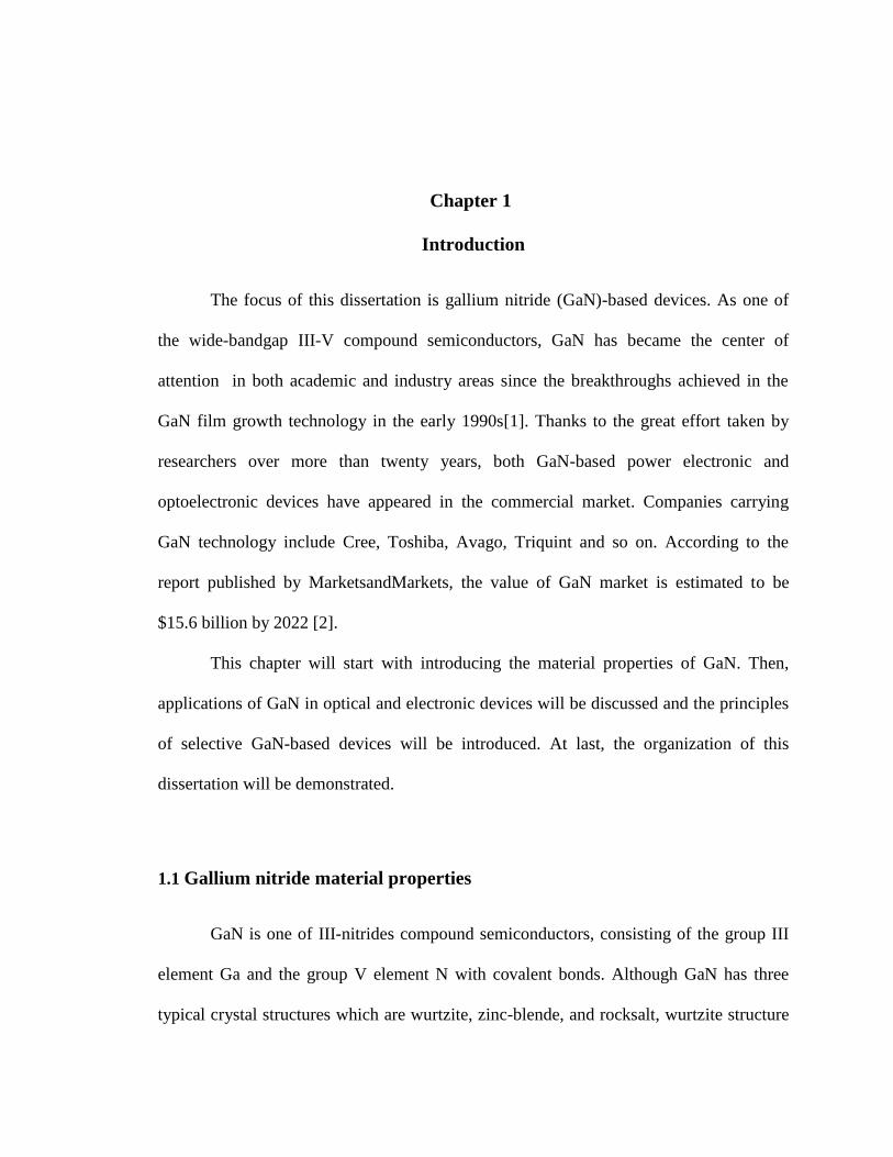
1.1 Gallium nitride material properties
GaN is one of III-nitrides compound semiconductors, consisting of the group III
element Ga and the group V element N with covalent bonds. Although GaN has three
typical crystal structures which are wurtzite, zinc-blende, and rocksalt, wurtzite structure
2
is the most common structure under equilibrium conditions because its
thermodynamically stability [3]. The basic unit cell of the wurtzite structure is shown in
Fig. 1-1. It is a hexagonal unit with two lattice constants, which are the hexagon edge
length a and the unit cell height c. For wurtzite GaN, a=3.189 Å and c =5.185 Å [4].
Figure 1-1. Wurtzite structures of GaN.
The synthesized GaN was first obtained in 1932 [5]. The reaction product
between the ammonia (NH3) gas and the metallic gallium at high temperature turns out a
dark grey powder. The GaN powder was turned to be impressive stable under ambient
conditions. The decomposition temperature of was suggested in the range of 750 oC and
1000 oC [6]. It was reported that GaN could not dissolve in general acids or bases at room
temperature but showed slow dissolution rate in hot concentrated H2SO4 and NaOH
solutions [4]. Due to the advanced thermal stability, GaN can withstand high
3
temperatures in device fabrication processes. However, the chemical stability of GaN
makes conventional wet etching technologies not suitable as etching method in GaN
material system [7]. Thus, dry etching technologies are commonly used in GaN device
fabrication processes.
In 1969, the first single GaN crystal was grown successfully by Maruska and
Tietjen. The GaN film was on sapphire using the hydride vapor phase epitaxy (HVPE)
technique [6]. The single crystalline GaN layers were obtained through reacting gallium
chloride (GaCl) with NH3 at 850 oC. The unintentionally doped GaN films contained high
inherent electron concentrations, which made the GaN films were n-type material. The
research of GaN material was almost stagnated due to the difficulties of restraining the
large intrinsic electron concentration and obtaining high quality conductive p-type GaN
for forming p-n junctions [1]. Almost ten years later, Amano et al. [9, 11] and Nakamura
et al. [10, 12] sucessefully got high quality GaN layers as well as conductive p-type GaN
by metal organic chemical vapor deposition (MOCVD) technique. As like breaking
through the bottlenecks, these improvements of GaN technology greatly boosted the
research on GaN-based devices since 1990s and this prosperity endures to nowadays.
GaN is a direct wide-bandgap (WBG) material. Figure 1-2 shows the
corresponding relation between the bandgap energy and the lattice constant for several
semiconductors [32, 35]. This figure shows that compared with Si and GaAs, both GaN
and SiC have a much larger bandgap, which are 3.44 eV and 3.26 eV respectively. GaN
and its alloys have a wide rang of bandgap energies occupying a continuous value from
1.9eV to 6.2eV, corresponding to a continuous wavelength from 635nm to 200nm. This
wavelength range covers the whole visible spectrum and extends to deep ultraviolet
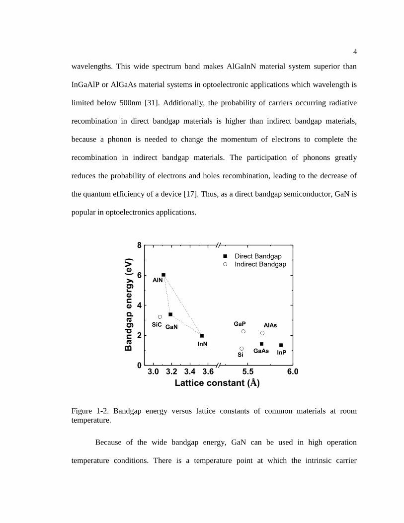
4
wavelengths. This wide spectrum band makes AlGaInN material system superior than
InGaAlP or AlGaAs material systems in optoelectronic applications which wavelength is
limited below 500nm [31]. Additionally, the probability of carriers occurring radiative
recombination in direct bandgap materials is higher than indirect bandgap materials,
because a phonon is needed to change the momentum of electrons to complete the
recombination in indirect bandgap materials. The participation of phonons greatly
reduces the probability of electrons and holes recombination, leading to the decrease of
the quantum efficiency of a device [17]. Thus, as a direct bandgap semiconductor, GaN is
popular in optoelectronics applications.
3.0 3.2 3.4 3.6 5.5 6.00
2
4
6
8
GaP AlAs
InPGaAsSi
SiC GaN
InN
Ba
nd
ga
p e
ne
rgy
(e
V)
Lattice constant (Å)
Direct Bandgap
Indirect Bandgap
AlN
Figure 1-2. Bandgap energy versus lattice constants of common materials at room
temperature.
Because of the wide bandgap energy, GaN can be used in high operation
temperature conditions. There is a temperature point at which the intrinsic carrier
5
concentration in a material will be high enough leading to the failure of devices,
generating a large amount of leakage current and losing their ability to control the carrier
density [8]. Since such temperature value is in direct proportion to the bandgap of a
material, GaN has a much lower intrinsic carrier density than those conventional narrow
bandgap materials such as Si and GaAs in a wide temperature range [47]. Therefore,
GaN-based devices could withstand the high temperature operation conditions.
Also, GaN has a relatively higher electric breakdown field than conventional
semiconductors due to its large bandgap. The electric breakdown field has a positive
correlation with the bandgap energy, according to the study conducted by Jerry et al. [9].
The critical electric field of GaN is estimated as ~5 MV/cm [10]. The large electric
breakdown field indicates that GaN material can withstand high supply voltage, which is
demanded in power electronic devices.
Moreover, GaN owns excellent carrier transport properties which relate directly to
the performance of electronic and optoelectronic devices. Excellent carrier transport
properties such as high electron mobility and large electron saturation velocity are
required for high frequency and high power applications. The measured electron mobility
for GaN is lower than 1000 cm2/V-s [10, 15]. Nevertherless, AlGaN/GaN
heterostructures have electron mobility of 2000 cm2/v-s and the two dimensional electron
gas (2DEG) with a sheet density of 1×13 cm-2
[16]. The availability of AlGaN/GaN
heterostructures combined with the 2DEG, which has a high sheet density and reasonable
electron mobility enables GaN a promising material for fast switching power electronics.
Another attractive property of GaN is its high thermal conductivity. Good thermal
conductivity guarantees an excellent performance of the device at high operation
6
temperature. The thermal conductivity value of GaN is 1.3 W/cm-K [11], which is similar
as the most common conventional material Si, but much higher than GaAs [15]. SiC has
a better thermal conductivity [15], than GaN, so GaN on SiC substrate is a good choice
for high power applications.
The fundamental material properties at room temperature associated the
performance of optoelectronic and electric devices for several semiconductors are listed
in Table 1-1.
Table 1-1. Properties of common materials at room temperature [1, 9-15].
Properties GaN
(AlGaN/GaN) SiC Si
GaAs
(AlGaAs/InGaAs)
Bandgap energy,
Eg (eV) 3.45 3.26 1.12 1.43
Electric
breakdown field,
Ec (MV/cm)
3.3 2.0 0.3 0.4
Saturated
electron velocity,
ʋsat (×107 cm/s)
2.5 2 1 1
Electron
mobility, μn
(cm2/V-s)
900
(>2000) 700 1500
8500
(10000)
2DEG density,
ns (×1013
cm-2
) 1 NA NA <0.2
Thermal
conductivity,
κ (W/cm-K)
1.3 4.5 1.5 0.5
7
1.2 Epitaxial GaN film growth
Three main techniques are used for GaN epitaxial growth, which are hydride
vapor phase epitaxy (HVPE), metal organic chemical vapor deposition (MOCVD), and
molecular beam epitaxy (MBE). HVPE is the first technology to grow epitaxial GaN
films by Maruska and Tietjen in 1969 [18], and was the most popular epitaxial GaN
growth technique in the 1970s [33]. This technique can grow high quality epitaxial GaN
layers at high growth rates above 100 um/h [34]. Furthermore, the low pressure and low
temperature conditions in the HVPE growth process make it a favorable technique for
GaN epitaxial growth [19]. Currently, HVPE is thought to be a highly promising
technique for growing thick GaN native substrate [18, 35]. MOCVD has been considered
to be the most popular and efficient method in epitaxial GaN growth since the high
quality GaN layers were successfully obtained by using this method in 1986 [36].
MOCVD is a growth technique with a low growth rate and can be used to grow
heterostructures due to the good control ability [1]. Moreover, the Ga/N flux ratio is very
low in MOCVD process, which could greatly reduce the nitrogen vacancies in the GaN
layers. MBE was first introduced for growing GaN by Gotoh et al. in 1981 by reacting
Ga with NH3 [37]. The process of MBE is under ultra-high vacuum (UHV) growth
conditions and can be controlled as precise as one atomic layer [37]. The high cleanliness
of the UHV chamber makes it possible to grow high purity GaN lattices. However, it is
difficult to find a nitrogen source for MBE system because the temperature for MBE
growth is too low to decompose NH3. Therefore, electron cyclotron resonance or radio
8
frequency plasmas are generally integrated in MBE systems to provide the nitrogen
source [1].
Generally, GaN films are grown on foreign substrates because of the absence of
the native GaN substrate. Lattice mismatch, thermal expansion coefficient (TEC)
mismatch, thermal conductivity, electrical conductivity, and price are on the list for
choosing a suitable substrate. Large lattice mismatch and TEC mismatch will lead a high
defect density. Since sapphire is an insulating substrate and has a low cost, it is the
traditional most common substrate for growing GaN [1]. But its high lattice mismatch,
high TEC mismatch, and bad thermal conductivity make it mainly used in GaN LEDs
[19]. SiC owns a very good thermal conductivity and relative low lattice mismatch and
TEC mismatch, which makes it a premium substrate for GaN-based high power
applications such as HEMTs. The disadvantage of SiC is the relatively high cost.
Although Si has large lattice mismatch and TEC mismatch as well as low thermal
conductivity, it is still on the choice list for GaN epitaxial growth because of the
possibility to integrate with other conventional Si devices [1].
Meanwhile, although heteroepitaxial GaN growth on foreign substrate works well
for most of GaN devices, the growth of bulk GaN substrate is also under intensive
research for improving the GaN device performance [34, 19]. GaN films grown on GaN
substrate are expected to have reduced defect density due to the elimination of the lattice
and TEC mismatching [34]. The recent achievements in growing native GaN substrate
techniques includes 3 inch freestanding GaN wafer with the lowest unintentional doping
of 1×10¹⁶
cm-3
obtained by HVPE technique, 2 inch wafer with the lowest unintentional
doping of 2×10¹⁸
cm-3
obtained by Ammono-thermal technique, and 1×10¹⁶
cm-3
obtained
9
by Na-solution growth technique [19]. Despite the big progress in bulk GaN growth, the
quality and the size of GaN substrate still could not meet the market requirements and the
price is extremely expensive [34, 48]. Therefore, most of GaN-based devices in
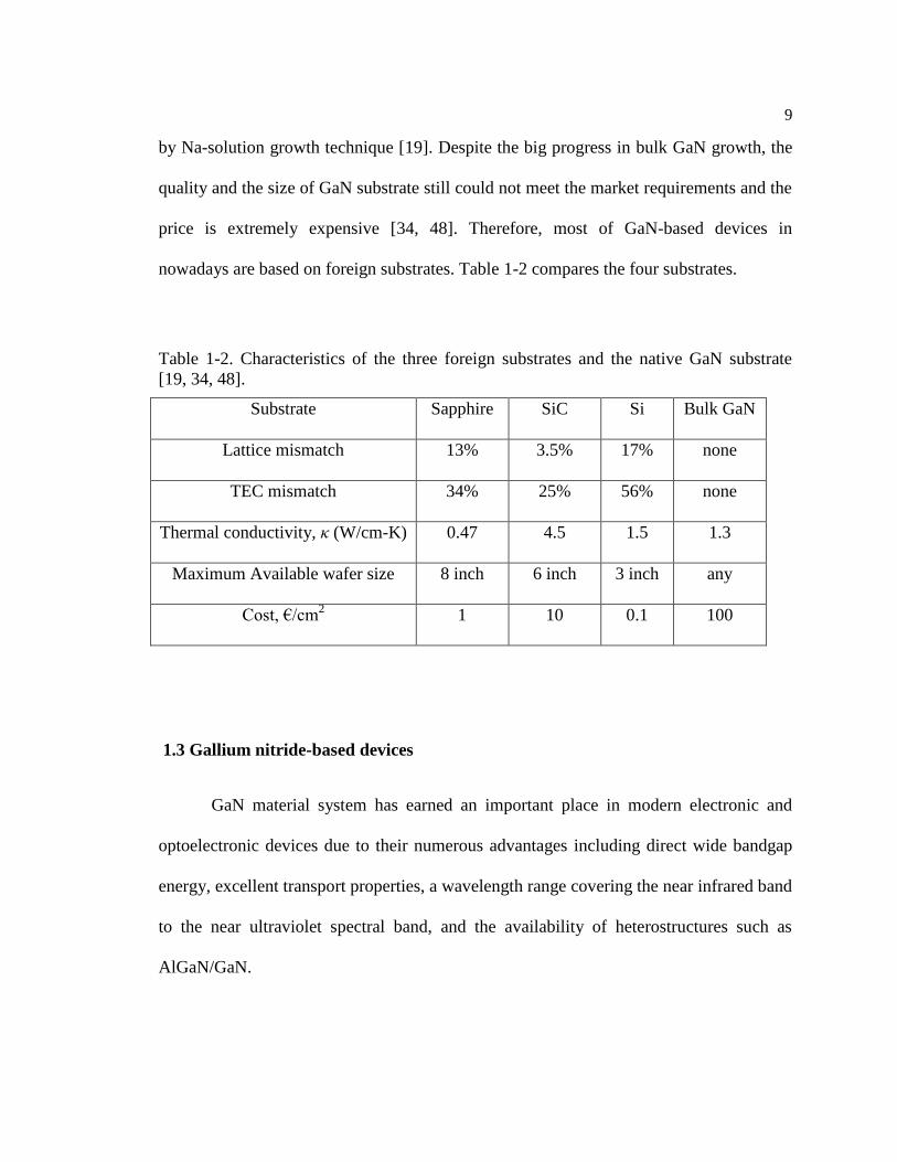
nowadays are based on foreign substrates. Table 1-2 compares the four substrates.
Table 1-2. Characteristics of the three foreign substrates and the native GaN substrate
[19, 34, 48].
Substrate Sapphire SiC Si Bulk GaN
Lattice mismatch 13% 3.5% 17% none
TEC mismatch 34% 25% 56% none
Thermal conductivity, κ (W/cm-K) 0.47 4.5 1.5 1.3
Maximum Available wafer size 8 inch 6 inch 3 inch any
Cost, €/cm2 1 10 0.1 100
1.3 Gallium nitride-based devices
GaN material system has earned an important place in modern electronic and
optoelectronic devices due to their numerous advantages including direct wide bandgap
energy, excellent transport properties, a wavelength range covering the near infrared band
to the near ultraviolet spectral band, and the availability of heterostructures such as
AlGaN/GaN.
1.3.1 Power Electronic devices
Currently, energy consumed in the world wide is mainly in the form of electrical
energy and most of the dissipated energy in a power electronic system is associated with
the power semiconductor devices [45]. Thus, there is a great interest in increasing the
efficiency of power electronic devices to minimize the consumed electrical energy.
Nowadays, the power electronic system largely depends on the Si-based semiconductor
devices. However, the maximum blocking voltage capability of current commercial Si
devices is lower than 7kV, and many Si devices can only operate under 200 oC. Si-based
devices also suffer an inadequate capacity of current conductance and a low switching
frequency [38]. These limitations of Si devices promote the development of wide
bandgap semiconductor-based electronic devices. Compared with the traditional Si-based
devices, wide bandgap material based electronic devices own enormous potential to
achieve higher energy conversion efficiency resulting in the reduction of device size,
cost, and energy consuming [46].
Among the wide bandgap semiconductor materials, GaN and SiC with mature and
well established process technologies are in the focus of attention and the most attractive
to the future development of power electronic devices [46]. GaN and SiC have very
similar material properties that provide them the capability of withstanding high reverse
voltage, high operation frequencies, and high temperature operation. However, GaN has
superior theoretical characteristics than SiC and is expected to demonstrate better
performance in high-power microwave applications [38, 46]. Figure 1-3 is a summary of
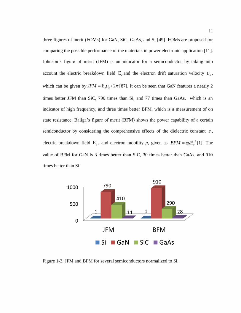
11
three figures of merit (FOMs) for GaN, SiC, GaAs, and Si [49]. FOMs are proposed for
comparing the possible performance of the materials in power electronic application [11].
Johnson’s figure of merit (JFM) is an indicator for a semiconductor by taking into
account the electric breakdown field c and the electron drift saturation velocity s ,
which can be given by / 2c sJFM [87]. It can be seen that GaN features a nearly 2
times better JFM than SiC, 790 times than Si, and 77 times than GaAs. which is an
indicator of high frequency, and three times better BFM, which is a measurement of on
state resistance. Baliga’s figure of merit (BFM) shows the power capability of a certain
semiconductor by considering the comprehensive effects of the dielectric constant ,
electric breakdown field c , and electron mobility μ, given as 3
cBFM [1]. The
value of BFM for GaN is 3 times better than SiC, 30 times better than GaAs, and 910
times better than Si.
Figure 1-3. JFM and BFM for several semiconductors normalized to Si.
JFM BFM
0
500
1000
1 1
790 910
410 290
11 28
Si GaN SiC GaAs
12
GaN-based optoelectronic devices have already been widely commercialized in
the market, while GaN-based power electronic devices are still at the beginning stage in
the commercial market [48]. As wide bandgap materials, GaN has a large electric
breakdown field (~5 MV/cm) and the ability to withstand high supply voltages and high
operation temperatures, which are required in power electronic devices [47]. Another
interesting property of GaN for power electronics is the availability of heterostructures
and the two-dimensional electron gas (2DEG) formed due to the polarization effects in
nitrides. High 2DEG sheet density and not too low electron mobility combined with high
electron saturation velocity (~2×10⁷
cm/s) enable GaN based devices to provide high
output currents and fast switching frequency, which are necessary elements for high-
power microwave devices [1]. These material properties evidently show that GaN is the
most promising candidate in power electronic applications.
There is a steady increasing interest to GaN-based power electronic devices in
industry nowadays and GaN has huge potential from wireless devices, power supplies,
and aerospace in the low voltage area to rail transport, smart power grid, and wind mills
in the high voltage area [50]. In a high voltage power electronic system, three-terminal
switches and two-terminal rectifiers are two essential components from the power
generation applications to custom power devices. For GaN-based power devices,
Schottky barrier diodes fulfill the two-terminal rectifier requirement and AlGaN/GaN
HEMTs perform as switches.
GaN SBDs with breakdown voltages higher than 600V were first reported and
commercialized by Liu et al. in 2009 [70]. The devices were grown on sapphire substrate
and had the leakage current as low as 200uA at the reverse voltage lower than 600V.
13
Meanwhile, forward current achieves 6A at 1.7V at room temperature. Breakdown
voltage of GaN SBDs as high as 1.5 kV have been demonstrated on Si substrate in 2013
by Boles et al. [71]. Although most of the reported GaN SBDs nowadays are lateral or
quasi-vertical structures, SBDs fabricated on bulk GaN substrates have been reported
owning several advantages over other foreign substrates [19, 46]. High breakdown
voltage SBDs on bulk GaN substrates have been reported and a low specific on-state
resistance of 1.1 mΩcm2 was achieved [72]. The quality of schottky contacts on GaN is
still a main concern in improving the performance of GaN SBDs. Defects and
contaminants induced in device fabrication processes as well as the native oxide will
cause the lowering of Schottky barrier height and deteriorate the ideal characteristics of
SBDs. Surface cleaning pretreatments including HNO3/HCl, HF/H2O, HCl/H2O, and
NH4OH solutions have been verified as effective ways to dissolve the oxide layer on the
GaN surface [73-75]. It also has been revealed by X-ray photoemission spectroscopy
analysis that KOH could effectively increase the band bending and improve the surface
stoichiometry of GaN Schottky contacts by removing the gallium atoms and the
chemisorbed oxygen atoms [76].
Currently, the most common nitride power electronic devices serving as switches
are GaN-based HEMTs. Thay have several advantages including the availability of
AlGaN/GaN heterostructures and the polarization effects induced 2DEG with high charge
density and acceptable electron mobility. Thus, GaN-based HEMTs well suited for high-
power microwave devcies and attract lots of entention both in academic and industry in
recent years [46]. Significant advancements have been achieved since the first
AlGaN/GaN HEMTs were proposed in 1994 [77]. A great deal of effect was made to
14
suppress the drain current degradation problem observed in GaN-based HEMTs. It is
thought that this current collapse is caused by the surface donor-like traps which have
low mobility and act like a “virtual gate”. This leads to the increase of the channel
resistance and consequently the reduction of the drain current [45, 78]. One main method
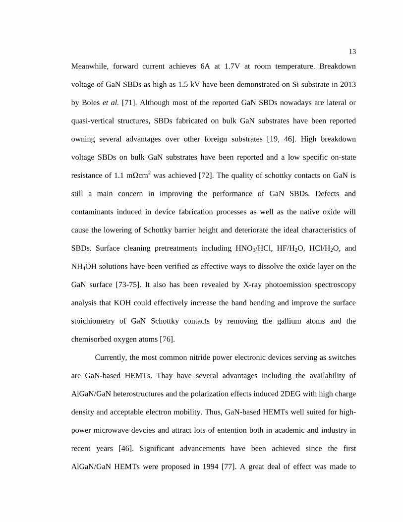
to prevent the current collapse is to add a field plate structure to relax the electric field
strength, as shown in Fig. 1-4 [79]. Other structures including a thin GaN cap structure,
the recessed gate structure, and the passivation film are also often used in AlGaN/GaN
for eliminating the current collapse [46].
Figure 1-4. A diagram of a GaN HEMT with a field plate structure.
Another research effort involved in the development of GaN-based HEMT
technologies is the development of normally-off GaN power switching transistors. It is
known that AlGaN/GaN HEMTs are normally-on devices due to the polarization induced
2DEG, allowing GaN HEMTs conducting current without gate bias. For safety reason,
normally-off switches are preferred in power applications, so it is desired to obtain
normally-off GaN HEMTs. One of the most used methods to achieve the normally-off
operation is to extend the gate into the barrier layer [82]. In this way, the AlGaN barrier
15
layer becomes very thin (2~5 nm) [45]. The thin AlGaN layer causes the elimination of
2DEG and a positive threshold voltage. The second method is to induce immobile
negative charges by injecting plasma treatment underneath the gate region to reduce the
2DEG. Thus, the threshold voltage would increase to a positive value [83]. Another
approach involves the use of p-n junction gate structure to form a depletion region in the
AlGaN layer [84].
1.3.2 Optoelectronic devices
III-nitride material system has tunable direct bandgap energies, which cover the
rang of from ~2 eV to ~6.2eV. This bandgap energy range corresponds to a wavelength
range from ~650 nm to ~300 nm which spans the whole spectral bands of near infrared,
visible, and deep ultraviolet [47]. The excellent material properties of GaN, such as
chemical stability, reasonable thermal conductivity, and high electron saturation drift
velocity, provide GaN great potential in power electronic applications also guarantee it to
be a promising material in optoelectronic devices.
The common materials used for LEDs include AlGaAs, InAlGaP, GaAsP, and
GaN [28]. GaN material system covers the widest visible spectrum range from violet to
red. Moreover, GaN and its alloys are the unique materials to provide emission with the
wavelength shorter than 500nm.
The first application of GaN in optoelectronics is LEDs, which also are the first
GaN-based devices. The first GaN LED emitting blue light with the peak wavelength of
475 nm was fabricated using metal-insolated-semiconductor structure in 1971 by
16
Pankove et al. [51]. With the achievements of GaN growth techniques and the
improvements of GaN epixycial layers, GaN LEDs based on pn junction structures and
high brightness blue double heterostructrues were proposed in 1989 and in 1993
respectively [43, 44]. The appearance of GaN blue LEDs opens a door to the white solid
state lighting, which was expected to be advanced over current incandescent and
fluorescent lighting techniques in energy saving, longer lifetime, and smaller size [52].
White solid-state lighting can be produced either by integrating LEDs, producing
red color, green color, and blue color separately, into a same package to obtain a mixing
white light or by using a phosphor in the GaN-based LED package to produce a white
emission by converting and mixing the blue light [14]. Figure 1-5 shows the two ways in
creating white light. The color-mixing method has a higher cost than the phosphor-based
white LED method and the color rendering is not good [14]. Meanwhile, due to the low
quality of green LEDs, the white LEDs based on color-mixing method has a lower
performance than the expectation [53]. On the other hand, the phosphor method earns a
lot of interest due to the low cost and compact package size. One of the popular
phosphor-based white LED techniques involves converting the blue emission from
InGaN/GaN multiple quantum-well (MQW) LEDs into yellow light to generate white
light [85]. Another way is to use an ultraviolet LED to pump a wide spectrum phosphor
for white light production [47]. Recently, quantum dots (QDs) have been used as
phosphor in the solid state white light technique due to their great features of sharp
absorption spectrum, excellent photoluminescence efficiency, and the wide emission
wavelength range[86]. Also, the discovery that the existence of nonradiative energy
transfer between InGaN/GaN QWs and QDs, which is believed a high efficiency color
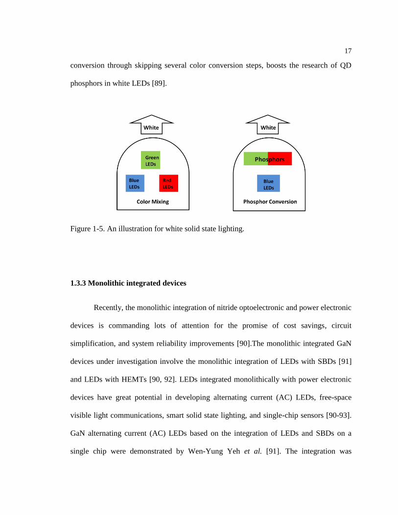
17
conversion through skipping several color conversion steps, boosts the research of QD
phosphors in white LEDs [89].
Figure 1-5. An illustration for white solid state lighting.
1.3.3 Monolithic integrated devices
Recently, the monolithic integration of nitride optoelectronic and power electronic
devices is commanding lots of attention for the promise of cost savings, circuit
simplification, and system reliability improvements [90].The monolithic integrated GaN
devices under investigation involve the monolithic integration of LEDs with SBDs [91]
and LEDs with HEMTs [90, 92]. LEDs integrated monolithically with power electronic
devices have great potential in developing alternating current (AC) LEDs, free-space
visible light communications, smart solid state lighting, and single-chip sensors [90-93].
GaN alternating current (AC) LEDs based on the integration of LEDs and SBDs on a
single chip were demonstrated by Wen-Yung Yeh et al. [91]. The integration was
18
expected to be achieved by the re-growth of SBD epi-layers on the LED epi-wafers or the
LED epi-layers on the SBD wafers. The monolithic integration of GaN-based LEDs and
GaN-based HEMTs was reported by Li et al. [92]. The integrated devices were fabricated
by growing LED epi-layers on customized AlGaN/GaN HEMT layers firstly and then
etching off certain regions of the LED epi-layers to expose the HEMTs areas. Lately, Liu
et al. [90] presented and compared two ways in fabricating monolithic integration of
LEDs and HEMTs in GaN. The LED-HEMT integration devices were realized through
the selective epitaxial removal (SER) method, which refers to grow the HEMT structure
on the LED structure followed by etching off selective areas to expose the LED region,
and the selective epitaxial growth (SEG) method, which refers to grow the HEMT
structure on selective region of the LED structure. The comparison results showed that
LEDs had better performance in the SEG method due to the avoidance of etching
processes [90]. Despite these achievements obtained in the GaN-based monolithic
integration devices, plenty of efforts are still needed to improve the integration
technologies due to the difficulty and complexity of integration fabrication processes
[90].
19
1.4 Fundamentals of selective Gallium nitride-based devices
1.4.1 Schottky barrier diodes
Schottky barrier height
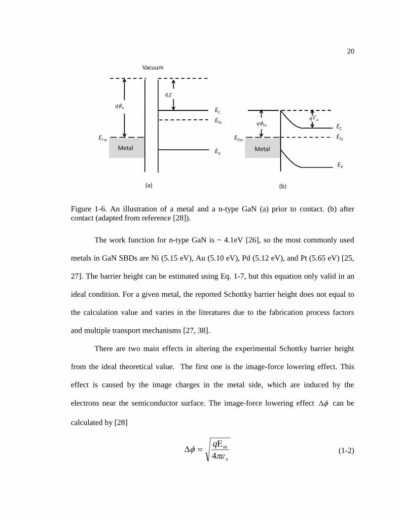
A Schottky barrier diode is a semiconductor diode which consists of rectifying
metal-semiconductor junctions [24]. A metal-semiconductor junction is made by a metal
contacting with a semiconductor. Figure 1-6 shows the energy band diagram of a metal
and an n-type GaN prior to and after contact. Metals with higher work function than the
work function of GaN are required for n-type semiconductor to form rectifying contacts
[28]. Before contact, the smaller work function of GaN makes the Fermi level in GaN
side is higher than the one in the metal side. After contact, the Fermi levels should be
constant at thermal equilibrium condition, leading to a barrer formed at the metal-GaN
interface. Ideally, the Schottky barrier height could simply be calculated by
subtracting the electron affinity of the semiconductor χ from the work function of the
metal and, as [25]
= ) (1-1)
. The energy band of the semiconductor near the interface appears distortion due to the
continuity of the vacuum level. The magnitude of this band bending is the built-in
potential [28].
20
Figure 1-6. An illustration of a metal and a n-type GaN (a) prior to contact. (b) after
contact (adapted from reference [28]).
The work function for n-type GaN is ~ 4.1eV [26], so the most commonly used
metals in GaN SBDs are Ni (5.15 eV), Au (5.10 eV), Pd (5.12 eV), and Pt (5.65 eV) [25,
27]. The barrier height can be estimated using Eq. 1-7, but this equation only valid in an
ideal condition. For a given metal, the reported Schottky barrier height does not equal to
the calculation value and varies in the literatures due to the fabrication process factors
and multiple transport mechanisms [27, 38].
There are two main effects in altering the experimental Schottky barrier height
from the ideal theoretical value. The first one is the image-force lowering effect. This
effect is caused by the image charges in the metal side, which are induced by the
electrons near the semiconductor surface. The image-force lowering effect can be
calculated by [28]
s
mq
4
(1-2)
21
, where [61]
)/(2
qkTVVqN
bi
S
m
(1-3)
is the maximum electric field at the interface, s is the dielectric constant of GaN, k the
Boltzmann constant, T the Kelvin temperature, q the electron charge, biV the built-in
potential, V the applied voltage, and N the doping concentration near the GaN surface.
Because of the built-in potential, the image-force lowering happens even at zero bias.
The second effect is the interface states effect. The existence of interface states in
the narrow interfacial layer with a thickness of a few angstroms and transparent to
electrons could alter the barrier height by pinning the semiconductor Fermi level at a
fixed position [28]. The relation between the barrier height and the interface states
density is found to be [25]
)]([)(21
)( 0000 bm
it
inbs
it
bgqD
NqqD
qqE
(1-4)
, where gE is the bandgap of the semiconductor, 0q is the surface potential below
which all states are donor states and above which are acceptor states, i is the
permittivity of vacuum, is the thickness of the interfacial layer, and itD is the interface
states density.
In the case of itD , the barrier height )(1
00 qEq
gb is a fixed value. On
the other hand, in the case of 0itD , the barrier height )(0 mb is the same as
the ideal barrier height calculated by Eq. 1-1 [25].
22
An index is proposed to evaluate the degree to which the barrier height is tailored
by interface states. This index is given by [62]
)(
0
m
b
d
dS (1-5)
. The value of S is between 0 and 1. S = 0 corresponds to the situation that the barrier
height is completely pinned by interface states, while S =1 corresponds to the situation
that the interface states do not exist. S is ~0.385 in GaN material, indicating a partial
pinning by interface states [62].
Carrier transport mechanism
Different from p-n junction diodes, under which the current mechanism is the
diffusion of minority carriers, the current in SBD is controlled by the drift of majority
carriers [25]. The current in GaN SBDs is produced by the transition of electrons between
the metal and GaN. The observed total current I transporting through the interface is the
algebraic sum of is the current density transfer from GaN to metal and the current density
transfer from metal to GaN [61].
In a moderately doped GaN, thermionic emission process is the dominant current
transport mechanism. Assuming kT and under the thermal equilibrium condition,
the total thermionic emission current at the interface is [63]
]1)[exp( nkT
qVII stotal (1-6)
, where sI is the reverse saturation current and is given by [25]
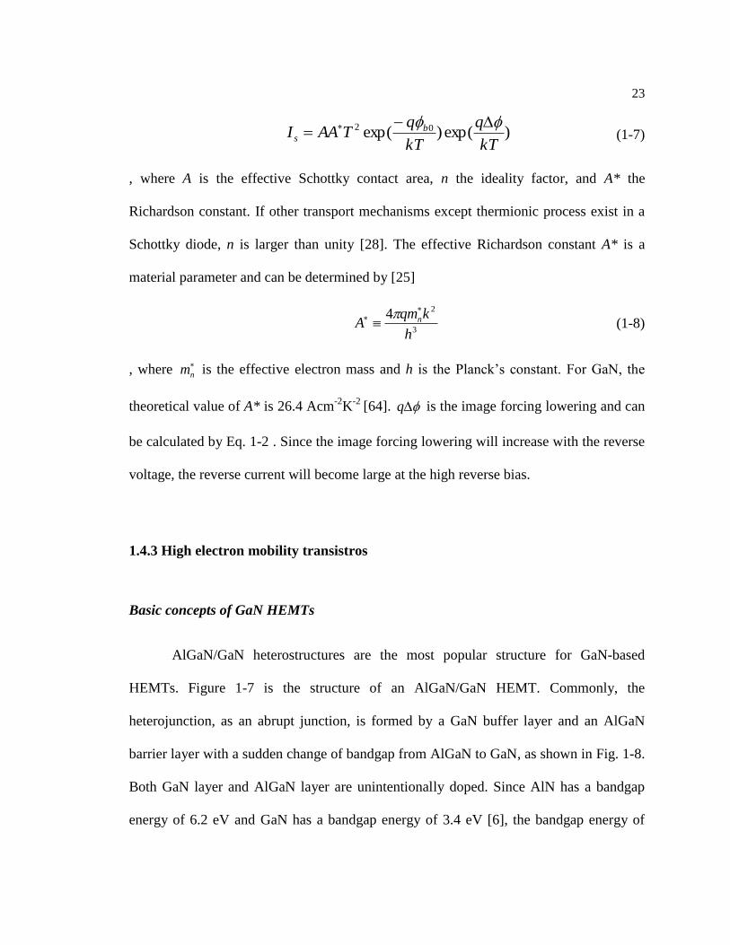
23
)exp()exp( 02
kT
q
kT
qTAAI b
s
(1-7)
, where A is the effective Schottky contact area, n the ideality factor, and A* the
Richardson constant. If other transport mechanisms except thermionic process exist in a
Schottky diode, n is larger than unity [28]. The effective Richardson constant A* is a
material parameter and can be determined by [25]
3
24
h
kqmA n
(1-8)
, where
nm is the effective electron mass and h is the Planck’s constant. For GaN, the
theoretical value of A* is 26.4 Acm-2
K-2
[64]. q is the image forcing lowering and can
be calculated by Eq. 1-2 . Since the image forcing lowering will increase with the reverse
voltage, the reverse current will become large at the high reverse bias.
1.4.3 High electron mobility transistros
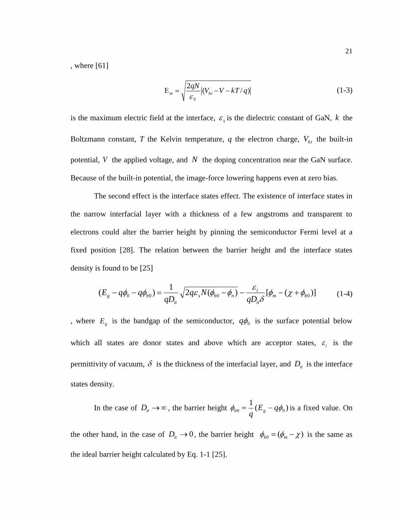
Basic concepts of GaN HEMTs
AlGaN/GaN heterostructures are the most popular structure for GaN-based
HEMTs. Figure 1-7 is the structure of an AlGaN/GaN HEMT. Commonly, the
heterojunction, as an abrupt junction, is formed by a GaN buffer layer and an AlGaN
barrier layer with a sudden change of bandgap from AlGaN to GaN, as shown in Fig. 1-8.
Both GaN layer and AlGaN layer are unintentionally doped. Since AlN has a bandgap
energy of 6.2 eV and GaN has a bandgap energy of 3.4 eV [6], the bandgap energy of
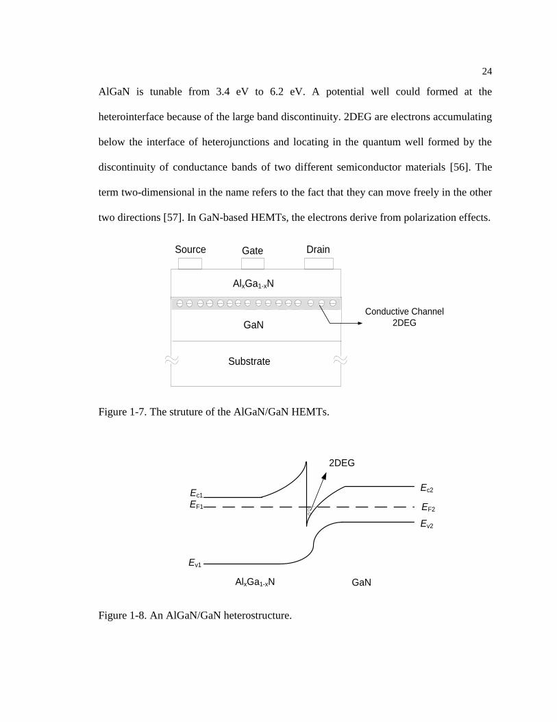
24
AlGaN is tunable from 3.4 eV to 6.2 eV. A potential well could formed at the
heterointerface because of the large band discontinuity. 2DEG are electrons accumulating
below the interface of heterojunctions and locating in the quantum well formed by the
discontinuity of conductance bands of two different semiconductor materials [56]. The
term two-dimensional in the name refers to the fact that they can move freely in the other
two directions [57]. In GaN-based HEMTs, the electrons derive from polarization effects.
Source Gate Drain
Conductive Channel
2DEG
AlxGa1-xN
GaN
Substrate
Figure 1-7. The struture of the AlGaN/GaN HEMTs.
Ec1
Ev1
EF1
Ec2
EF2
Ev2
2DEG
AlxGa1-xN GaN
Figure 1-8. An AlGaN/GaN heterostructure.
25
Two dimensional electron gas in AlGaN/GaN HEMTs
There are two types of polarization effects in III-nitrides like GaN, AlN, and InN
due to the existence of nitrogen atoms. First effect is spontaneous polarization which
induced by the fact that no electron occupies the outer orbital of a nitrogen atom leading
to the strong Coulomb attraction force between the atomic nucleus and the surrounding
electrons [58]. Thus, in III-nitride covalent bonds, all electrons will be attracted to the
nitrogen atom side. This causes the appearance of strong iconicity in the III-nitride
covalent bonds [38]. At last, the nitrogen atom demonstrates negative charge and the
gallium (Ga) atom demonstrates positive charge in a gallium-nitrogen covalent bond due
to this iconicity. For the whole asymmetry wurtzite GaN crystal, a macroscopic
polarization will be produced, named as spontaneous polarization [59].
Another polarization effect is piezoelectric polarization effect. This type of
polarization is induced by the external stress from the mismatch of the lattice constants
between two materials [58]. An important issue involves in the formation of
heterostructures is the matching of the lattice constants in two different materials. An
epitaxial growth film will be strained if the lattice constant of the substrate is differeent
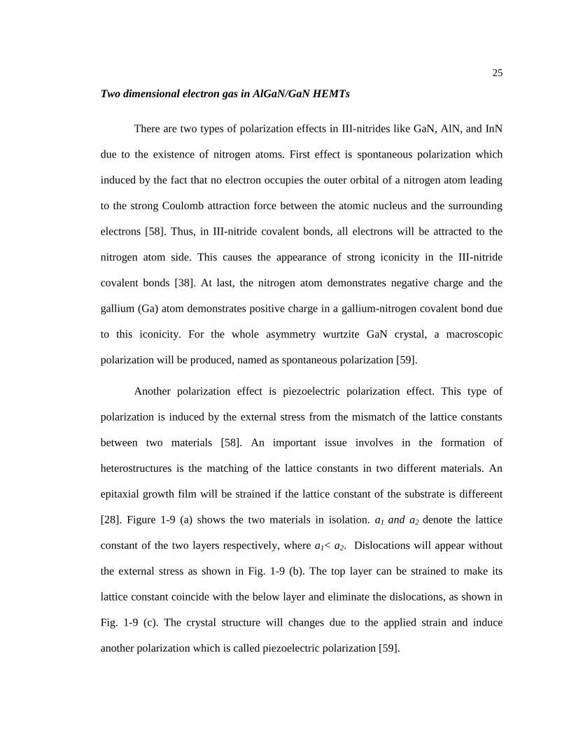
[28]. Figure 1-9 (a) shows the two materials in isolation. a1 and a2 denote the lattice
constant of the two layers respectively, where a1< a2. Dislocations will appear without
the external stress as shown in Fig. 1-9 (b). The top layer can be strained to make its
lattice constant coincide with the below layer and eliminate the dislocations, as shown in
Fig. 1-9 (c). The crystal structure will changes due to the applied strain and induce
another polarization which is called piezoelectric polarization [59].
26
straina1
(a)
a2
(b) (c)
Figure 1-9. (a) Separated (b) Thick epitaxial layer (c) Thin epitaxial layer.
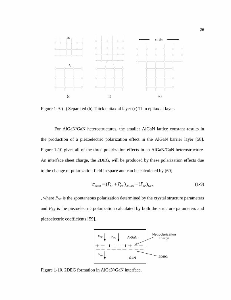
For AlGaN/GaN heterostructures, the smaller AlGaN lattice constant results in
the production of a piezoelectric polarization effect in the AlGaN barrier layer [58].
Figure 1-10 gives all of the three polarization effects in an AlGaN/GaN heterostructure.
An interface sheet charge, the 2DEG, will be produced by these polarization effects due
to the change of polarization field in space and can be calculated by [60]
GaNSPAlGaNPESPsheet PPP )()( (1-9)
, where PSP is the spontaneous polarization determined by the crystal structure parameters
and PPE is the piezoelectric polarization calculated by both the structure parameters and
piezoelectric coefficients [59].
PSP PPE
PSP
AlGaN
GaN
Net polarization
charge
2DEG
Figure 1-10. 2DEG formation in AlGaN/GaN interface.
27
Principles of operation
GaN-based HEMTs are normally-on devices. The 2DEG formed by polarization
effects in the potential well serves as a conductive current channel in a GaN HEMT,
under the control of the applied gate voltage. By using complete depletion approximation,
the relationship of the 2DEG density ns below the heterojunction and the gate voltage VGS
can be demonstrated by [65-67]
( )Fs GS th
En V V
qd q
(1-10)
, where is the dielectric constant of AlGaN, d is the thickness of the AlGaN layer, EF
the Fermi energy, and Vth threshold voltage.
To calculate the drain current of HEMT devices, one needs to consider the
modulation on drain current by both drain voltage and gate voltage. Using the gradual
channel approximation, the charge control model can be modified to [68]
( ) ( ( ))s GS thn z V V V zqd
(1-11)
, where V(z) is the channel potential.
In the non-saturation region, the electron velocity is dependent on the distance
apart from the source z:
( )( ) n
dV zv z
dz (1-12)
, where µn is the electron mobility. Assuming a constant electron mobility µn, the drain
current is described by [67]
28
2
[( ) ]2
n g DSDS GS th DS
g
W VI V V V
dL
(1-13)
, where Lg is the gate length, Wg the gate width, and VDS the bias.
Under the hgih drain voltage VDS condition, the 2DEG density near the drain
terminal is close to zero. The channel becomes “pinch-off”. Meanwhile, the drain current
tends to saturation and is given by [28]
2( )n g
Dsat GS th
g
u WI V V
dL
(1-14)
1.4.3 Light emitting diodes
Principles of LEDs
Conventionally, incandescent lamps and fluorescent lamps are used for
luminescence. In incandescent lamps, the visible light comes from the heated filament
[29], while fluorescent lamps emit visible light by the absorption of phosphors to the UV
light [30]. Unlike those traditionally luminescence technologies, LEDs emit the light
directly through the radiative recombination process of electrones and holes.
The operation principle of LEDs is spontaneous emission. Electrons and holes can
experience either radiative recombination or non radiative recombination in the energy
gap of a semiconductor, as illustrated in Fig. 1-11 [40]. The energy is released as
electromagnetic wave in the radiative recombination process, while transferred to other
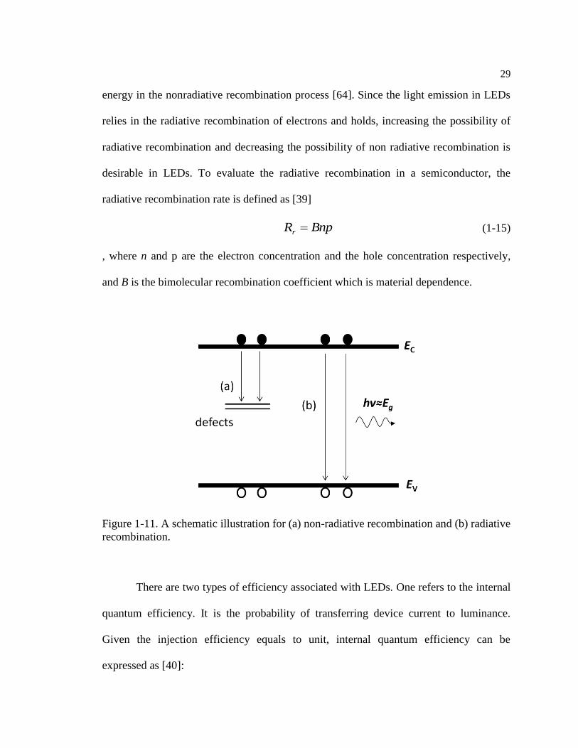
29
energy in the nonradiative recombination process [64]. Since the light emission in LEDs
relies in the radiative recombination of electrons and holds, increasing the possibility of
radiative recombination and decreasing the possibility of non radiative recombination is
desirable in LEDs. To evaluate the radiative recombination in a semiconductor, the
radiative recombination rate is defined as [39]
BnpRr (1-15)
, where n and p are the electron concentration and the hole concentration respectively,
and B is the bimolecular recombination coefficient which is material dependence.
Figure 1-11. A schematic illustration for (a) non-radiative recombination and (b) radiative
recombination.
There are two types of efficiency associated with LEDs. One refers to the internal
quantum efficiency. It is the probability of transferring device current to luminance.
Given the injection efficiency equals to unit, internal quantum efficiency can be
expressed as [40]:
30
nrr
nri
(1-16)
, where r is the radiative lifetime and nr is the nonradiative lifetime. nr should be kept
longer than r to get a high internal quantum efficiency. Reducing the defect and
impurity densities in the semiconductor is an effective way to prolong the nonradiative
lifetime nr [40].
The other efficiency is the external quantum efficiency ex , which defined as [28]
opinex (1-17)
, where op is the optical efficiency. op relies on the device optic characteristics and
does not depends on the electrical characteristics [28]. The external quantum efficiency
valuates how much light has been extracted out from devices.
Similar as a normal p-n junction diode, electrons in the n-type semiconductor side
will diffuse into the p-type side. A depletion region will be formed in an equilibrium
condition. Under the forward bias condition, carriers are injected into the depletion
region. They can recombine to each other either in radiative pathway or nonradiative
pathway [39]. A radiative recombination process is characterized by releasing the energy
as photons. The bandgap of the semiconductor determins the wavelength of the generated
light λ, which is given by [40]
)(24.1
umEgap
(1-18)
, where Egap is the bandgap energy of a semiconductor material. Thus, a specific
semiconductor material should be selected to get lamination with a certain color.
31
Multiple quantum well InGaN/GaN LEDs
The first GaN-based LED was formed by insert insulator between a metal and a
GaN layer due to the unavailability of p-type GaN in early 1970s [41, 42]. Later, in 1989
Amano et al. [43] proposed the first p-n junction GaN LED. High brightness double
heterostructure GaN LEDs were firstly reported in 1993 by Nakamura et al. [44]. In the
double heterostructure GaN LEDs, electrons and holes are confined in a narrow potential
well. Increasing the number of electrons and holes can short the radiative recombination
time and result in an increase of efficiency of LEDs [28]. However, double
heterostructure LEDs do not have a wide wavelength range and the InGaN layer need to
be Zn doped [38]. Also, the thick recombination region in the double heterostructue
LEDs will cause unnecessarily energy losses due to the long traveling path of the light
[69]. To overcome these disadvantages of double heterostructure LEDs, the width of the
InGaN layer was reduced to the order of the de Broglie wavelength, typically smaller
than 10nm [28]. This narrow potential well is referred as a quantum well in which
carriers can only move freely in two directions that are perpendicular to the crystal
growth direction. Since the thickness of the quantum well is extremely small, the
epitaxial layers can tolerate large lattice mismatch and consequently have less defects
[28]. On the other hand, electron and holes are easily to be saturated in the limited
volume of a single quantum well, leading to the overflow of extra carriers. Therefore, the
single quantum well is repeated in several periods and comprises the multiple quantum
wells (MQWs) to hold the extra carriers overflowing from the adjacent quantum well
[80].
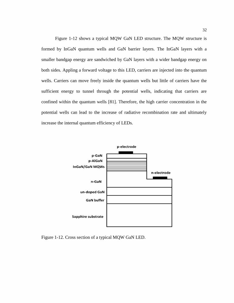
32
Figure 1-12 shows a typical MQW GaN LED structure. The MQW structure is
formed by InGaN quantum wells and GaN barrier layers. The InGaN layers with a
smaller bandgap energy are sandwiched by GaN layers with a wider bandgap energy on
both sides. Appling a forward voltage to this LED, carriers are injected into the quantum
wells. Carriers can move freely inside the quantum wells but little of carriers have the
sufficient energy to tunnel through the potential wells, indicating that carriers are
confined within the quantum wells [81]. Therefore, the high carrier concentration in the
potential wells can lead to the increase of radiative recombination rate and ultimately
increase the internal quantum efficiency of LEDs.
Figure 1-12. Cross section of a typical MQW GaN LED.
33
1.5 Organization of the Dissertation
The rest part of this dissertation is organized as below.
Chapter 2 demonstrates the successful fabrication of GaN SBDs with high voltage
blocking capability and low on-state voltage on commercial LED epi-wafers.
Chapter 3 investigates the transfer saturation feature of GaN-based HEMTs.
Chapter 4 focuses on the design and modeling of DG HEMTs featuring enhanced
back gate-control of the 2DEG in AlGaN/GaN heterostructures.
Chapter 5 studied the temperature-dependent electrical properties of GaN HEMTs
over a cryogenic temperature range.
Chapter 6 is concerned with the design of QDs coupled non-resonant microcavity
LEDs with micro-holes to enhance non-radiative energy transfer between QDs and
InGaN/GaN QWs for the first time by tailoring the radiative relaxiation lifetime of
electron-hole pairs in QW.
Chapter 7 discusses the future work on the study of the GaN/patterned sapphire
substrate interface region and the on-chip integration of LEDs and MESFETs in GaN.
34
Reference
1. Mark C.J.C.M. Kramer, “Gallium Nitride-based Microwave High-Power
Heterostructure Field-Effect Transistors: design, technology, and characterization,”
Technische Universiteit Eindhoven, 2006.
2. Marketsandmarkets.com, “Gallium Nitride (GaN) Semiconductor Devices (Discrete
& IC) and Substrate Wafer Market by Technology, Application, Product, Device, &
by Geography - Forecast & Analysis to 2013 - 2022”, marketsandmarkets.com,
March 2014.
3. Jacques I. Pankove, Theodore D. Moustakas, Robert K. Willardson, and Eicke R.
Weber “Gallium-Nitride (GaN) II”, Academic Press, October 30, 1998.
4. Xiao-Feng Zhang and Ze Zhang, “Progress in Transmission Electron Microscopy 2:
Applications in Materials Science”, Springer, 2001 edition, October 19, 2010.
5. W.C. Johnson, J.B. Parson and M.C. Crew, “Nitrogen Compounds of Gallium III.
Gallic Nitride”, J. Phys. Chem. 36, 2561 (1932).
6. Hadis Morkoç, “Nitride Semiconductors and Devices,” Springer, September 28,
1999.
7. Takafumi Yao and Soon-Ku Hong, “Oxide and Nitride Semiconductors: Processing,
Properties, and Applications”, Springer Science & Business Media, Mar 20, 2009.
8. Committee on Materials for High-Temperature Semiconductor Devices, Commission
on Engineering and Technical Systems, National Materials Advisory Board, Division
on Engineering and Physical Sciences, National Research Council, “Materials for
High-Temperature Semiconductor Devices,” National Academies, Sep 28, 1995.
35
9. J. L. Hudgins, G. S. Simin, E. Santi, and M. Asifkhan, “An Assessment of Wide
Bandgap Semiconductors for Power Devices”, IEEE Trans. Power Electronics, vol.
18, pp. 907 –914, 2003.
10. Michael E. Levinshtein, Sergey L. Rumyantsev and Michael S. Shur, “Properties of
Advanced Semiconductor Materials: GaN, AIN, InN, BN, SiC, SiGe,” John Wiley &
Sons, Feb 21, 2001.
11. L. M. Tolbert, B. Ozpineci, S. K. Islam, and M. S. Chinthavali, “Wide bandgap
semiconductors for utility applications,” in Proc. Power and Energy Systems. ACTA
Press, USA, Feb. 2003.
12. M. A. Littlejohn, J. R. Hauser and T. H. Glisson, “Monte Carlo Calculation of
Velocity-Field Relationship for Gallium Nitride,” Applied Physics Letters, Vol. 26,
No. 11, 1975, pp. 625-627.
13. B. Gelmont, K. Kim, and M. Shur, J. Appl. Phys. 74, 1818, 1993.
14. Shuji Nakamura and Michael R. Krames, “History of Gallium–Nitride-Based Light-
Emitting Diodes for Illumination”, Proceedings of the IEEE, Vol. 101, No. 10,
October 2013.
15. K. Shenai, R.S. Scott, and B.J. Baliga, “Optimum Semiconductor for High-Power
Electronics”, IEEE Trans. Electron Devices, vol. ED-36, pp. 1811-1823, 1989.
16. R. T. Kemerley, H. B. Wallace, and M. N. Yoder, “Impact of wide bandgap
microwave devices on DoD systems,” Proceedings of the IEEE, vol. 90, pp. 1059–
1064, June 2002.
17. M. SATHISH KUMAR, “FUNDAMENTALS OF OPTICAL FIBRE
COMMUNICATION,” PHI Learning Pvt. Ltd., Jan 1, 2005.
36
18. H. P. Maruska and J. J. Tietjen, “The preparation and properties of vapor-deposited
single-crystalline GaN,” Appl. Phys. Lett., vol. 15, pp. 327–329, Nov. 1969.
19. T. Paskova, D. A. Hanser, and K. R. Evans, “GaN substrates for III-nitride devices,”
Proc. IEEE, vol. 98, no. 7, pp. 1324–1338, Jul. 2010.
20. H. Amano, M. Kito, K. Hiramatsu, and I. Akasaki, “p-type conduction in Mg-doped
GaN treated with low-energy electron beam irradiation (LEEBI),” Jpn. J. Appl. Phys.,
vol. 28, pp. L2112–L2114, Dec. 1989.
21. H. Amano, N. Sawaki, I. Akasaki, and Y. Toyoda, “Metalorganic vapor phase
epitaxial growth of a high quality GaN film using AlN buffer layer,” Appl. Phys.
Lett., vol. 48, pp. 353–355, Feb. 1986.
22. S. Nakamura, T. Mukai, M. Senoh, and N. Iwasa, “Thermal annealing effects on p-
type Mg-doped GaN films,” Jpn. J. Appl. Phys., vol. 31, pp. L139–L142, Feb. 1992.
23. S. Nakamura, “In situ monitoring of GaN growth using interference effects,” Jpn. J.
Appl. Phys., vol. 30, no. 8, pp. 1620–1627, Aug. 1991.
24. NANDITA DASGUPTA and AMITAVA DASGUPTA, “SEMICONDUCTOR
DEVICES: MODELLING AND TECHNOLOGY”, PHI Learning Pvt. Ltd., Jan 1,
2004.
25. Donald Neamen , “Semiconductor Physics and Devices”, McGraw-Hill, 2011.
26. Kathryn A. Minder, “Aluminum Gallium Nitride UV Optoelectronic Devices: Device
Design, Fabrication and Characterization”, ProQuest, 2008.
27. Q.Z. Liu and S.S. Lau, “A review of the metal–GaN contact technology”, Solid-State
Electronics, Volume 42, Issue 5, 6 May 1998, Pages 677–691.
37
28. Simon M. Sze and Kwok K. Ng, “Physics of Semiconductor Devices”, Wiley-
Interscience, October 27, 2006.
29. http://en.wikipedia.org/wiki/Incandescent_light_bulb.
30. http://en.wikipedia.org/wiki/Fluorescent_lamp.
31. S.J. Pearton, F. Ren, A.P. Zhang and K.P. Lee, “Fabrication and performance of GaN
electronic devices,” Materials Science and Engineering: R: Reports Volume 30,
Issues 3–6, 1 December 2000, Pages 55–212.
32. http://www.ioffe.ru/SVA/NSM/Semicond/.
33. Wei Zhang and B. K. Meyer, “Growth of GaN quasi-substrates by hydride vapor
phase epitaxy”, physica status solidi (c), Volume 0, Issue 6, pages 1571–1582,
September 2003.
34. Tanya Paskova and Keith R. Evans, “GaN Substrates—Progress, Status, and
Prospects,” IEEE JOURNAL OF SELECTED TOPICS IN QUANTUM
ELECTRONICS, VOL. 15, NO. 4, JULY/AUGUST 2009.
35. http://www.semiconductors.co.uk/propiiiv5653.htm.
36. Stephen J. Pearton, “GaN and Related Materials, Volume 1,” CRC Press, Oct 29,
1997.
37. Hideki Gotoh, Toru Suga, Hideo Suzuki and Morihiko Kimata, “Low Temperature
Growth of Gallium Nitride,” Jpn. J. Appl. Phys. 20 L545, 1981.
38. S. J. Pearton, J. C. Zolper, R. J. Shul and F. Ren, “GaN: Processing, defects, and
devices”, J. Appl. Phys. 86, 1 (1999).
38
39. Jian-Jang Huang, Hao-Chung Kuo, and Shyh-Chiang Shen, “Nitride Semiconductor
Light-Emitting Diodes (LEDs): Materials, Technologies and Applications”,
Woodhead Publishing, Feb 14, 2014.
40. Shuji Nakamura and Shigefusa F. Chichibu, “Introduction to Nitride Semiconductor
Blue Lasers and Light Emitting Diodes”, CRC Press, Mar 9, 2000.
41. J. I. Pankove, E. A. Miller, D. Richman, and J. E. Berkeyheiser,
‘‘Electroluminescence in GaN,’’ J. Luminescence, vol. 4, pp. 63–66, 1971.
42. H. P. Maruska, D. A. Stevenson, and J. I. Pankove, ‘‘Violet luminescence of Mg-
doped GaN,’’ Appl. Phys. Lett., vol. 22, pp. 303–305, 1973.
43. H. Amano, M. Kito, K. Hiramatsu, and I. Akasaki, ‘‘p-type conduction in Mg-doped
GaN treated with low-energy electron beam irradiation (LEEBI),’’ Jpn. J. Appl.
Phys., vol. 28, pp. L2112–L2114, 1989.
44. S. Nakamura, M. Senoh, and T. Mukai, ‘‘p-GaN/n-InGaN/n-GaN double-
heterostructure blue-light-emitting diodes,’’ Jpn. J. Appl. Phys., vol. 32, pp. L8–L11,
1993.
45. Tetsu Kachi, “Current status of GaN power devices”, IEICE Electronics Express Vol.
10 (2013) No. 21 pp. 20132005.
46. J. Millan, P. Godignon, X. Perpinya, A. Perez-Tomas, and J. Rebollo, “A survey of
wide band gap power semiconductor devices,” IEEE Trans. Power Electron.,
Volume:29 , Issue: 5, 2013.
47. Mohamed Henini and M Razeghi, “Optoelectronic devices: III-nitrides”, Elsevier
Science; 1 edition, April 6, 2005.
39
48. Kaminski, N. and Hilt, O., “SiC and GaN devices - wide bandgap is not all the same”,
IET Circuits Devices Syst., 2014, Vol. 8, Iss. 3, pp. 227–236.
49. H. Ueda, M. Sugimoto, T. Uesugi, and T. Kachi, “Wide-Bandgap Semiconductor
Devices for Automobile Applications”, CS MANTECH Conference, April 24-27,
2006, Vancouver, British Columbia, Canada.
50. Krishna Shenai, Michael Dudley, and Robert F. Davis, “Current Status and Emerging
Trends in Wide Bandgap (WBG) Semiconductor Power Switching Devices”, ECS J.
Solid State Sci. Technol. 2013 volume 2, issue 8, N3055-N3063.
51. J. I. Pankove, E. A. Miller, and J. E. Berkeyheiser, RCA Review, vol. 32, p. 383,
1971.
52. S. Nakamura, M. Senoh, and T. Mukai, “p-GaN/n-InGaN/n-GaN double-
heterostructure bluelight- emitting diodes,” Jpn. J. Appl. Phys., vol. 32, pp. L8–L11,
Jan. 1993. (Artūras Žukauskas, Michael S. Shur, Remis Gaska, “Introduction to
Solid-State Lighting,” Wiley, Apr 18, 2002.)
53. Razeghi, M., Bayram, C.; Vashaei, Z. ; Cicek, E., McClintock, R., “III-Nitride
Optoelectronic Devices: From ultraviolet detectors and visible emitters towards
terahertz intersubband devices”, IEEE Photonics Society, 2010 23rd Annual Meeting
of the, 7-11 Nov. 2010,Page(s):351 – 352.
54. http://en.wikipedia.org/wiki/Field-effect_transistor
55. T. Ytterdal, Y. Cheng and T. A. Fjeldly, “Device Modeling for Analog and RF
CMOS Circuit Design”, Wiley, May 7, 2003.
56. http://en.wikipedia.org/wiki/2DEG
40
57. J. P. Ibbetson, P. T. Fini, K. D. Ness, S. P. DenBaars, J. S. Speck and U. K. Mishr,
Polarization effects, surface states, and the source of electrons in AlGaN/GaN
heterostructure field effect transistors, Appl. Phys. Lett. 77, 250 (2000).
58. Fabio Bernardini, Vincenzo Fiorentini, and David Vanderbilt, “Spontaneous
polarization and piezoelectric constants of III-V nitrides”, Phys. Rev. B 56,
R10024(R), 15 October 1997.
59. O. Ambacher, J. Smart, J. R. Shealy, N. G. Weimann, K. Chu, M. Murphy, W. J.
Schaff, L. F. Eastman, R. Dimitrov, L. Wittmer, M. Stutzmann, W. Rieger, and J.
Hilsenbeck, “Two-dimensional electron gases induced by spontaneous and
piezoelectric polarization charges in N- and Ga-face AlGaN/GaN heterostructures,”
1999 J. Appl. Phys. 85 3222.
60. Edward T. Yu, “III-V Nitride Semiconductors: Applications and Devices,” CRC
Press (September 6, 2002).
61. C.Y. Chang and S.M. Sze, “CARRIER TRANSPORT ACROSS METAL-
SEMICONDUCTOR BARRIERS”, Solid-State Electronics, Volume 13, Issue 6, June
1970, Pages 727–740.
62. I. Shalish, L. Kronik, G. Segal, Y. Shapira, M. Eizenberg, and J. Salzman, “Yellow
luminescence and Fermi level pinning in GaN layers,” Appl. Phys. Lett. 77, 987
(2000).
63. P. Hacke, T. Detchprohm, K. Hiramatsu, N. Sawaki, “Temperature variation of
current–voltage characteristics of Au/Ni/n-GaN Schottky diodes ,” Appl. Phys. Lett.
63 (1993), 2676.
64. Dilip K Roy, “Physics Of Semiconductor Devices (Rev.)”, Universities Press, 2004.
41
65. I. Saidi, M. Gassoumi, H. Mejri, C. Gaquière, H. Maaref, “Self-heating and trapping
effects in AlGaN/GaN heterojunction field-effect transistors”, J. Appl. Phys., 106
(2009), p. 054511.
66. Rashmi, Abhinav Kranti, S. Haldar, R.S. Gupta, “An accurate charge control model
for spontaneous and piezoelectric polarization dependent two-dimensional electron
gas sheet charge density of lattice-mismatched AlGaN/GaN HEMTs”, Solid-State
Electronics , Volume 46, Issue 5, May 2002, Pages 621–630.
67. Manel Charfeddine, Hafedh Belmabrouk, Mohamed Ali Zaidi, Hassen Maaref, “2-D
Theoretical Model for Current–Voltage Characteristics in AlGaN/GaN HEMT’s”,
Journal of Modern Physics, 2012, 3, 881-886.
68. Rashmi, Angu Agrawal, S. Sen, S. Haldar and R. S. Gupta, “Analytical model for dc
characteristics and small-signal parameters of AIGaN/GaN modulation-doped field-
effect transistor for microwave circuit applications”, Microwave and Optical
Technology Letters, Volume 27, Issue 6, pages 413–419, 20 December 2000.
69. Vinod Kumar Khanna, “Fundamentals of Solid-State Lighting: LEDs, OLEDs, and
Their Applications in Illumination and Displays,” CRC Press; 1 edition (June 3,
2014).
70. Lin Lin Liu et al., 2008, Materials Science Forum, 600-603, 1251.
71. Boles, T., Varmazis, C., Carlson, D., Palacios, T., Turner, G. W. and Molnar, R. J.
(2013), >1200 V GaN-on-silicon Schottky diode. Phys. Status Solidi C, 10: 835–839.
72. Taku Horii et al., 2009, Materials Science Forum, 615-617, 963.
73. Q. Z. Liu, L. S. Yu, F. Deng, S. S. Lau, Q. Chen, and M. A. Khan, Appl.Phys. Lett.
71, 1658 1997.
42
74. Q. Z. Liu, S. S. Lau, N. R. Perkins, and T. F. Kuech, Appl. Phys. Lett. 69, 1722 1996.
75. L. L. Smith, S. W. King, R. J. Nemanich, and R. F. Davis, J. Electron. Mater. 25, 805
1996.
76. P. B. Shah1, I. Batyrev, M. A. Derenge1, U. Lee, C. Nyguen1 and K. A. Jones,
“Schottky metal-GaN interface KOH pretreatment for improved device
performance”, J. Vac. Sci. Technol. A 28, 684 (2010).
77. M. A. Khan, J. N. Kuznia, D. T. Olson, W. J. Schaff, J. W. Burm, and M. S. Shur,
“Microwave performance of a 0.25 μm gate AlGaN/GaN heterostructure field effect
transistor,” Appl. Phys. Lett., vol. 65, pp. 1121– 1123, 1994.
78. Ramakrishna Vetury, Naiqain Q. Zhang, Stacia Keller, and Umesh K. Mishra, “The
Impact of Surface States on the DC and RF Characteristics of AlGaN/GaN HFETs”,
IEEE TRANSACTIONS ON ELECTRON DEVICES, VOL. 48, NO. 3, MARCH
2001.
79. Wataru Saito, Yorito Kakiuchi, Tomohiro Nitta, Yasunobu Saito, Takao Noda,
Hidetoshi Fujimoto, Akira Yoshioka, Tetsuya Ohno, and Masakazu Yamaguchi,
“Field-Plate Structure Dependence of Current Collapse Phenomena in High-Voltage
GaN-HEMTs,” IEEE ELECTRON DEVICE LETTERS, VOL. 31, NO. 7, JULY
2010.
80. E.F. Schubert, Light-Emitting Diodes, Cambridge University Press, New York, 2006.
81. Soon Jung, lgu Yun, Chang Myung Lee, Joo In Lee, Photoluminescence study of
InGaN/GaN multiple-quantum-well with Si-doped InGaN electron-emitting Layer,
Current Applied Physics Volume 9, Issue 5, September 2009, Pages 943–945.
43
82. Wataru Saito, Yoshiharu Takada, Masahiko Kuraguchi, Kunio Tsuda, and Ichiro
Omura, “Recessed-Gate Structure Approach Toward Normally Off High-Voltage
AlGaN/GaN HEMT for Power Electronics Applications,” IEEE TRANSACTIONS
ON ELECTRON DEVICES, VOL. 53, NO. 2, FEBRUARY 2006.
83. Yong Cai, Yugang Zhou, Kei May Lau, and Kevin J. Chen, “Control of Threshold
Voltage of AlGaN/GaN HEMTs by Fluoride-Based Plasma Treatment: From
Depletion Mode to Enhancement Mode”, IEEE TRANSACTIONS ON ELECTRON
DEVICES, VOL. 53, NO. 9, SEPTEMBER 2006.
84. X. Hu, G. Simin, J. Yang, M. Asif Khan, R. Gaska and M.S. Shur, “Enhancement
mode AIGaN/GaN HFET with selectively grown pn junction gate,” ELECTRONICS
LETTERS 13th April 2000 Vol. 36, No. 8.
85. S. Fujita, A. Sakamoto, S. Tanabe, Luminescence Characteristics of YAG Glass-
Ceramic Phosphor for White LED, Selected Topics in Quantum Electronics, IEEE
Journal of, 14 (2008) 1387-1391.
86. Günter Schmid, Nanoparticles: From Theory to Application, John Wiley & Sons, Jul
26, 2011.
87. B. JAYANT BALIGA, Power Semiconductor Device Figure of Merit for High-
Frequency Applications, IEEE ELECTRON DEVICE LETTERS, VOL. 10, NO. 10,
OCTOBER 1989.
88. S.J. Pearton, F. Ren, A.P. Zhang, K.P. Lee, Fabrication and performance of GaN
electronic devices, Materials Science and Engineering: R: Reports Volume 30, Issues
3–6, 1 December 2000, Pages 55–212.
44
89. M. Achermann, M. A. Petruska, S. Kos, D. L. Smith, D. D. Koleske, V. I. Klimov,
Energy-transfer pumping of semiconductor nanocrystals using an epitaxial quantum
well, Nature 2004, 429, 642.
90. Zhaojun Liu1, Jun Ma1, Tongde Huang1, Chao Liu1 and Kei May Lau, Selective
epitaxial growth of monolithically integrated GaN-based light emitting diodes with
AlGaN/GaN driving transistors,Appl. Phys. Lett. 104, 091103 (2014).
91. W.-Y. Yeh, H.-H. Yen, Y.-J. Chan, The development of monolithic alternating
current light-emitting diode, (2011) 793910-793910.
92. Z. Li, J. Waldron, T. Detchprohm, C. Wetzel, R.F. Karlicek, T.P. Chow, Monolithic
integration of light-emitting diodes and power metal-oxide-semiconductor channel
high-electron-mobility transistors for light-emitting power integrated circuits in GaN
on sapphire substrate, Applied Physics Letters, 102 (2013).
93. F.G. Kalaitzakis, E. Iliopoulos, c, G. Konstantinidis, N.T. Pelekanosa, Monolithic
integration of nitride-based transistor with Light Emitting Diode for sensing
applications, Microelectronic Engineering Volume 90, February 2012, Pages 33–36.
Chapter 2
High performance GaN Schottky Barrier Diodes (SBDs) on plasma deep-
etched surface
In this chapter, GaN SBDs with high voltage blocking capability and low on-state
voltage are successfully fabricated on commercial LED epi-wafers. Potassium hydroxide
(KOH) with optimized concentration is used to eliminate the inductively coupled plasma
(ICP) etching-induced surface defects for reducing the leakage current in SBDs.
Furthermore, the numerical values of the surface defect density for samples with and
without KOH treatment are extracted by analyzing the leakage current mechanism. At
last, GaN alternating current (AC) LEDs with monolithic integration of micro-LEDs and
SBDs are demonstrated.
2.1 Introduction
For decades the technology of III-nitride based devices has been under intense
investigation for the improved performance in various optical and electronic applications.
Recently, there have been growing interests in monolithic integration of III-nitride
optoelectronics and power electronics, and monolithically integrated light emitting diodes
(LEDs) with Schottky barrier diodes (SBDs) or high electron mobility transistors
(HEMTs) have been demonstrated and proposed for AC-LEDs, smart solid state lighting,
free-space visible light communication, and on-chip sensing applications [1-4]. The
monolithic LEDs could potentially reduce the cost and shrink the system size, but the
46
performance of the monolithic devices is often compromised by the processing
complexity and fabrication imperfection that are associated with the integration scheme
[3]. Among them, inductively coupled plasma (ICP) etching is indispensible removing
certain epitaxial layers of the LED epi-wafer to integrate electronic devices. However, the
physical ion bombardment involved in the ICP etching generates a damaged surface
region with the signature amounts of nitrogen vacancies at the GaN surface, since the
lighter nitrogen atoms are more readily to be removed than gallium atoms [5]. These
nitrogen vacancies combine with oxygen impurities which are absorbed by dangling
gallium bonds and act as donors with the activation energy of 30-40 meV [6, 7]. As a
result, the barrier height decreases due to the reduction of the band bending. Also, the
surface region becomes a degenerated n-type GaN layer which could facilitate the
electrons tunneling through the depletion region significantly. Both the band bending
reduction and the tunneling probability enhancement are responsible for the degeneration
of the devices. X-ray photoemission spectroscopy analysis has revealed that KOH could
effectively eliminate the induced donors on ICP damaged GaN surface to increase the
band bending and improve the surface stoichiometry through the removal of the gallium
atoms and the chemisorbed oxygen atoms, as well as the passivation of the dangling
gallium bonds by forming Ga-H bonds [8]. Although many previous reports have claimed
that the performance of GaN SBDs in terms of leakage current, ideal factor, and barrier
homogeneity is greatly improved after the KOH treatment [9-11], few GaN SBDs under
investigation is fabricated from a LED epi-wafer and undergoes a deep etching process
with the etched depth larger than 3 um. The research for the effect of KOH treatment on
deep ICP-etched GaN SBDs is still under demand.
47
In the following sections, the fabrication process of our GaN SBDs is described.
The effect of KOH with different solution concentration on the recovery of deep ICP-
damaged surface is compared and investigated. Furthermore, leakage current mechanism
is analyzed and the value of the surface defect density is extracted. In the end, GaN SBDs
fabricated on LED epi-wafers with breakdown voltage higher than 200V and their
applications in the AC-LEDs are demonstrated.
2.2 Experimental Methods
Figure 2-1 shows the SBDs fabricated on LED epi-wafers process flow. The
SBDs are fabricated on 2-inch commercial LED epi-wafers, which epitaxial structure
comprises, from top down, by a ~200 nm p-type (Na> 1×10¹⁸
cm-3
) GaN capping layer, a
~200 nm p-type (Na≈ 5×10¹⁷
cm-3
) GaN layer, a multiple quantum well (MQW) emissive
layer consisted by fifteen pairs of 2.5nm-In0.1Ga0.9N/12 nm-GaN, a ~2.4 um n-type (Nd ≈
1×10¹⁸
cm-3
) GaN layer, and a ~2.5 um GaN buffer layer on a patterned sapphire
substrate. The fabrication areas of SBDs are exposed by a Cl2/Ar ICP cyclic etching
process. After removing the up layers with a total thickness of ~3um, KOH treatment is
performed before the contact metal deposition. To optimize the performance of the SBDs
integrated on LED epi-wafers, the ICP-etched samples are treated by KOH with different
concentration. Samples are soaked into 0.1mole/L, 0.5mole/L, 1mole/L aqueous KOH
solution for 10min, and molten KOH for 90s respectively.
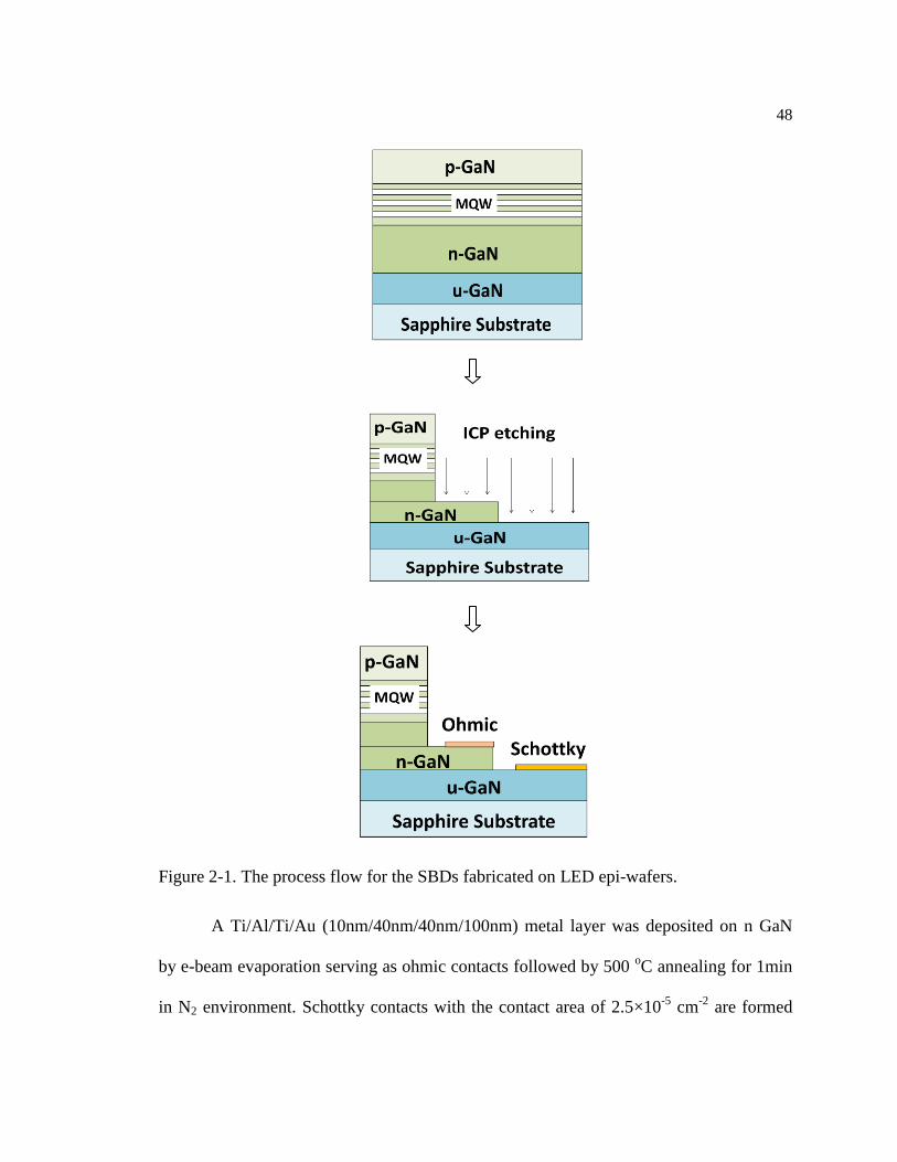
48
Figure 2-1. The process flow for the SBDs fabricated on LED epi-wafers.
A Ti/Al/Ti/Au (10nm/40nm/40nm/100nm) metal layer was deposited on n GaN
by e-beam evaporation serving as ohmic contacts followed by 500 oC annealing for 1min
in N2 environment. Schottky contacts with the contact area of 2.5×10⁻⁵
cm-2
are formed
49
by depositing Ni/Al/Ti/Au (50nm/500nm/100nm/200nm) on u-GaN layer. IV
characteristics of the SBDs are measured using a Keithley 2612 current source meter.
2.3 Results and Discussion
Figure 2-2 shows the dependences of the current density on voltage in the SBDs
treated by KOH with different concentrations under reverse bias. The samples treated by
KOH are obviously have reduced leakage current in compared with the control samples
which do not experience KOH treatment after ICP etching. This verifies that KOH
treatment is an effective way in eliminating the ICP-induced damage. However, the
degree of the effective does not in direct proportional to the KOH concentration. The
reverse voltages at the leakage current density of 10A/cm2
are 17V for the control sample,
48V for the 0.1 mole/L KOH treated sample, 90V for the 0.5 mole/L KOH treated-
sample, 59V for the 1 mole/L KOH treated sample, and 39V for the molten KOH treated-
sample, as shown in Fig. 2-3. It can be seen that the 0.5 mole/L KOH treated sample has
the highest reverse voltage value at a certain leakage current value, indicating that 0.5
mole/L KOH solution can best improve the ICP-damaged GaN surface.
50
-100 -80 -60 -40 -20 010
-9
10-7
10-5
10-3
10-1
101
103
105
1 mole KOH
0.5 mole KOH 0.1 mole KOH
molten KOH
Cu
rre
nt
De
ns
ity
(A
/cm
2)
Voltage (V)
control sample
Figure 2-2. J-V curves under reverse bias of GaN SBDs treated by KOH with different
concentration.
0.0 0.2 0.4 0.6 0.8 1.0 molten0
20
40
60
80
100
Re
ve
rse
vo
lta
ge
(V
)
KOH concentration (mole/L)
Figure 2-3. Reverse voltages as the function of KOH concentration at the leakage current
J=10 A/cm2.
AFM images were taken to inspect the KOH concentration dependent results.
Figure 2-4 (a) shows the AFM image for the control sample as well as the value of the
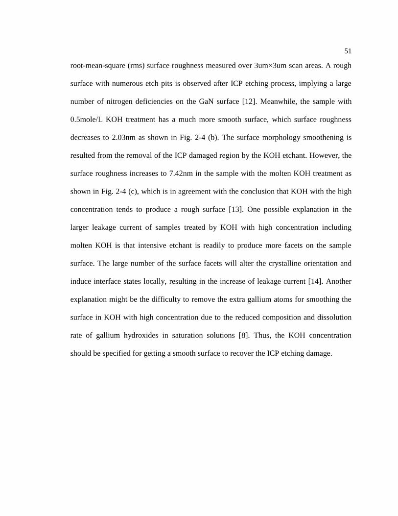
51
root-mean-square (rms) surface roughness measured over 3um×3um scan areas. A rough
surface with numerous etch pits is observed after ICP etching process, implying a large
number of nitrogen deficiencies on the GaN surface [12]. Meanwhile, the sample with
0.5mole/L KOH treatment has a much more smooth surface, which surface roughness
decreases to 2.03nm as shown in Fig. 2-4 (b). The surface morphology smoothening is
resulted from the removal of the ICP damaged region by the KOH etchant. However, the
surface roughness increases to 7.42nm in the sample with the molten KOH treatment as
shown in Fig. 2-4 (c), which is in agreement with the conclusion that KOH with the high
concentration tends to produce a rough surface [13]. One possible explanation in the
larger leakage current of samples treated by KOH with high concentration including
molten KOH is that intensive etchant is readily to produce more facets on the sample
surface. The large number of the surface facets will alter the crystalline orientation and
induce interface states locally, resulting in the increase of leakage current [14]. Another
explanation might be the difficulty to remove the extra gallium atoms for smoothing the
surface in KOH with high concentration due to the reduced composition and dissolution
rate of gallium hydroxides in saturation solutions [8]. Thus, the KOH concentration
should be specified for getting a smooth surface to recover the ICP etching damage.
52
(a)
(b)
(c)
Figure 2-4. AFM images of (a) the sample without KOH treatment. (b) the sample with
0.5mole/L KOH treatment. (c) the sample with molten KOH treatment.
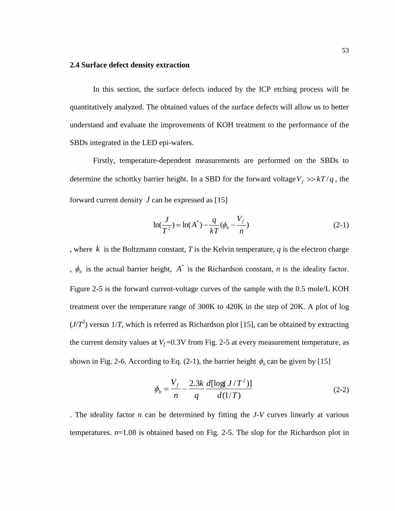
53
2.4 Surface defect density extraction
In this section, the surface defects induced by the ICP etching process will be
quantitatively analyzed. The obtained values of the surface defects will allow us to better
understand and evaluate the improvements of KOH treatment to the performance of the
SBDs integrated in the LED epi-wafers.
Firstly, temperature-dependent measurements are performed on the SBDs to
determine the schottky barrier height. In a SBD for the forward voltage qkTV f / , the
forward current density J can be expressed as [15]
)()ln()ln( *
2 n
V
kT
qA
T
J f
b (2-1)
, where k is the Boltzmann constant, T is the Kelvin temperature, q is the electron charge
, b is the actual barrier height, *A is the Richardson constant, n is the ideality factor.
Figure 2-5 is the forward current-voltage curves of the sample with the 0.5 mole/L KOH
treatment over the temperature range of 300K to 420K in the step of 20K. A plot of log
(J/T2) versus 1/T, which is referred as Richardson plot [15], can be obtained by extracting
the current density values at Vf =0.3V from Fig. 2-5 at every measurement temperature, as
shown in Fig. 2-6. According to Eq. (2-1), the barrier height b can be given by [15]
)/1(
)]/[log(3.2 2
Td
TJd
q
k
n
V f
b (2-2)
. The ideality factor n can be determined by fitting the J-V curves linearly at various
temperatures. n=1.08 is obtained based on Fig. 2-5. The slop for the Richardson plot in
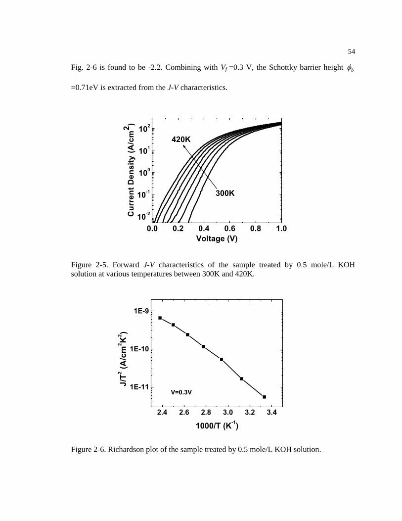
54
Fig. 2-6 is found to be -2.2. Combining with Vf =0.3 V, the Schottky barrier height b
=0.71eV is extracted from the J-V characteristics.
0.0 0.2 0.4 0.6 0.8 1.0
10-2
10-1
100
101
102
420K C
urr
en
t D
en
sit
y (
A/c
m2
)
Voltage (V)
300K
Figure 2-5. Forward J-V characteristics of the sample treated by 0.5 mole/L KOH
solution at various temperatures between 300K and 420K.
2.4 2.6 2.8 3.0 3.2 3.4
1E-11
1E-10
1E-9
J/T
2 (
A/c
m2K
2)
1000/T (K-1)
V=0.3V
Figure 2-6. Richardson plot of the sample treated by 0.5 mole/L KOH solution.
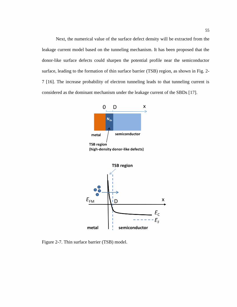
55
Next, the numerical value of the surface defect density will be extracted from the
leakage current model based on the tunneling mechanism. It has been proposed that the
donor-like surface defects could sharpen the potential profile near the semiconductor
surface, leading to the formation of thin surface barrier (TSB) region, as shown in Fig. 2-
7 [16]. The increase probability of electron tunneling leads to that tunneling current is
considered as the dominant mechanism under the leakage current of the SBDs [17].
Figure 2-7. Thin surface barrier (TSB) model.
56
Figure 2-8 is a energy band diagram for a SBD with a reverse bias Vr. Given
qkTVr / and most of the reverse current is the tunneling current, the reverse current
density Jr can be approximated as [18]
dVFTFk
TAJ rs
Vq
mr
b
))(1()(*
)(
0
(2-3)
, where q is the image force barrier lowering, bV is the built-in potential at the
reverse bias rV , mF and sF are the electron Fermi-Dirac distribution functions for the
metal and the semiconductor respectively, η is the electron energy below the effective
barrier, and )(T is the electron tunneling probability. Based on the Wentzel-Kramers-
Brillouin approximation, )(T can be expressed as [17]
])(2
2exp[)(
2
1
*
dxExqm
T
x
x
(2-4)
, where )(x is the surface potential profile, E is the electron energy, and x1 and x2 are
the classical turning points.
Assuming a triangular Schottky potential barrier profile which is [19]
0)( bqxqxq (2-5)
, where 0bq is the barrier height in the ideal condition. The electron tunneling
probability can be given by
])(2
3
4exp[)(
2
3
0
*
q
EqmET b
(2-6)
, where is the constant electric field near the top of the effective barrier, and E is
electron energy.
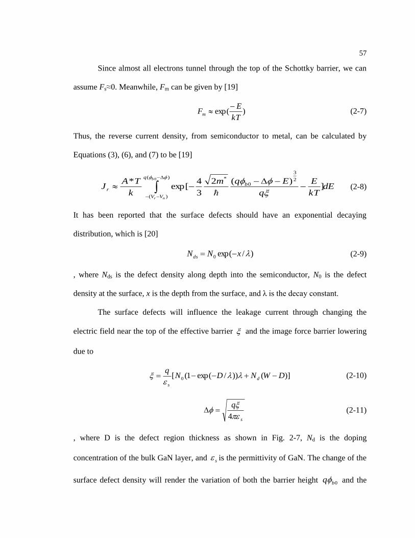
57
Since almost all electrons tunnel through the top of the Schottky barrier, we can
assume Fs≈0. Meanwhile, Fm can be given by [19]
)exp(kT
EFm
(2-7)
Thus, the reverse current density, from semiconductor to metal, can be calculated by
Equations (3), (6), and (7) to be [19]
dEkT
E
q
Eqm
k
TAJ
b
nr
q
VV
br
)(
)(
2
3
0
*0
])(2
3
4exp[
*
(2-8)
It has been reported that the surface defects should have an exponential decaying
distribution, which is [20]
)/exp(0 xNNds (2-9)
, where Nds is the defect density along depth into the semiconductor, N0 is the defect
density at the surface, x is the depth from the surface, and λ is the decay constant.
The surface defects will influence the leakage current through changing the
electric field near the top of the effective barrier and the image force barrier lowering
due to
)]())/exp(1([ 0 DWNDNq
d
s
(2-10)
s
q
4 (2-11)
, where D is the defect region thickness as shown in Fig. 2-7, Nd is the doping
concentration of the bulk GaN layer, and s is the permittivity of GaN. The change of the
surface defect density will render the variation of both the barrier height 0bq and the
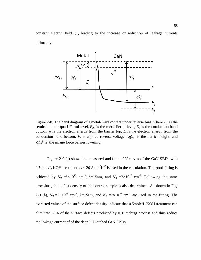
58
constant electric field , leading to the increase or reduction of leakage currents
ultimately.
Figure 2-8. The band diagram of a metal-GaN contact under reverse bias, where Ef is the
semiconductor quasi-Fermi level, Efm is the metal Fermi level, Ec is the conduction band
bottom, η is the electron energy from the barrier top, E is the electron energy from the
conduction band bottom, Vr is applied reverse voltage, 0bq is the barrier height, and
q is the image force barrier lowering.
Figure 2-9 (a) shows the measured and fitted J-V curves of the GaN SBDs with
0.5mole/L KOH treatment. A*=26 Acm-2
K-2
is used in the calculation. The good fitting is
achieved by N0 =8×10
17 cm
-3, λ=15nm, and Nd =2×10
16 cm
-3. Following the same
procedure, the defect density of the control sample is also determined. As shown in Fig.
2-9 (b), N0 =2×10
18 cm
-3, λ=15nm, and Nd =2×10
16 cm
-3 are used in the fitting. The
extracted values of the surface defect density indicate that 0.5mole/L KOH treatment can
eliminate 60% of the surface defects produced by ICP etching process and thus reduce
the leakage current of of the deep ICP-etched GaN SBDs.
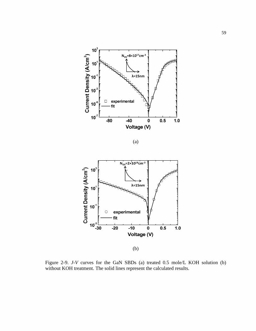
59
(a)
(b)
Figure 2-9. J-V curves for the GaN SBDs (a) treated 0.5 mole/L KOH solution (b)
without KOH treatment. The solid lines represent the calculated results.
60
2.5 High performance of Schottky barrier diodes
Through the optimized KOH treatment process, the breakdown voltages of the
SBDs fabricated on LED epi-wafers are in the range between 170V and 200V, larger
than 200V (the limit of our test equipment) for some devices. Figure 2-10 shows typical
J-V characteristics of the fabricated SBDs. The average reverse voltage Vr for the current
of -100uA in our devices is -170V, around 14 times the ones from the SBDs also
fabricated on LED epi-wafers but without KOH treatment for AC-LED rectifiers [1] and
for electrostatic discharge protection [21]. Meanwhile, the average forward on-state
voltage Vf for the current of 20mA in our devices is 3.1 V, comparable to the references,
which are 1.8 V and 2.8 V respectively. The comparison results are shown in Table 2-1.
Table 2-1.Compared results with other references [1, 21].
Vr (V) Vf (V) Reference
-11 1.8 1
-12 2.8 21
-170 3.1 This work
Moreover, the leakage current of our devices keeps below 1 uA at the reverse bias
of 100V, indicating high voltage blocking capability. The high breakdown voltages can
reduce the number of SBDs integrated in the system, minimizing the size of integration
chips and the power loss.
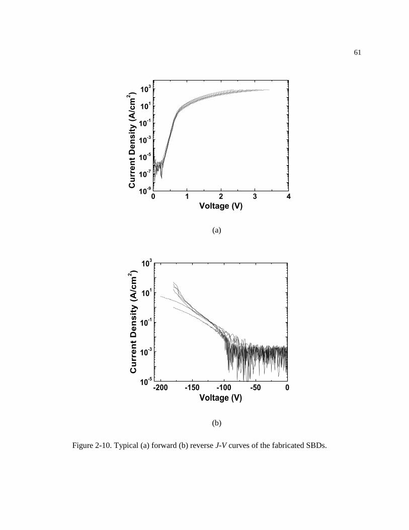
61
(a)
-200 -150 -100 -50 010
-5
10-3
10-1
101
103
Cu
rre
nt
De
ns
ity
(A
/cm
2)
Voltage (V)
(b)
Figure 2-10. Typical (a) forward (b) reverse J-V curves of the fabricated SBDs.
0 1 2 3 410
-9
10-7
10-5
10-3
10-1
101
103
Cu
rre
nt
De
ns
ity
(A
/cm
2)
Voltage (V)
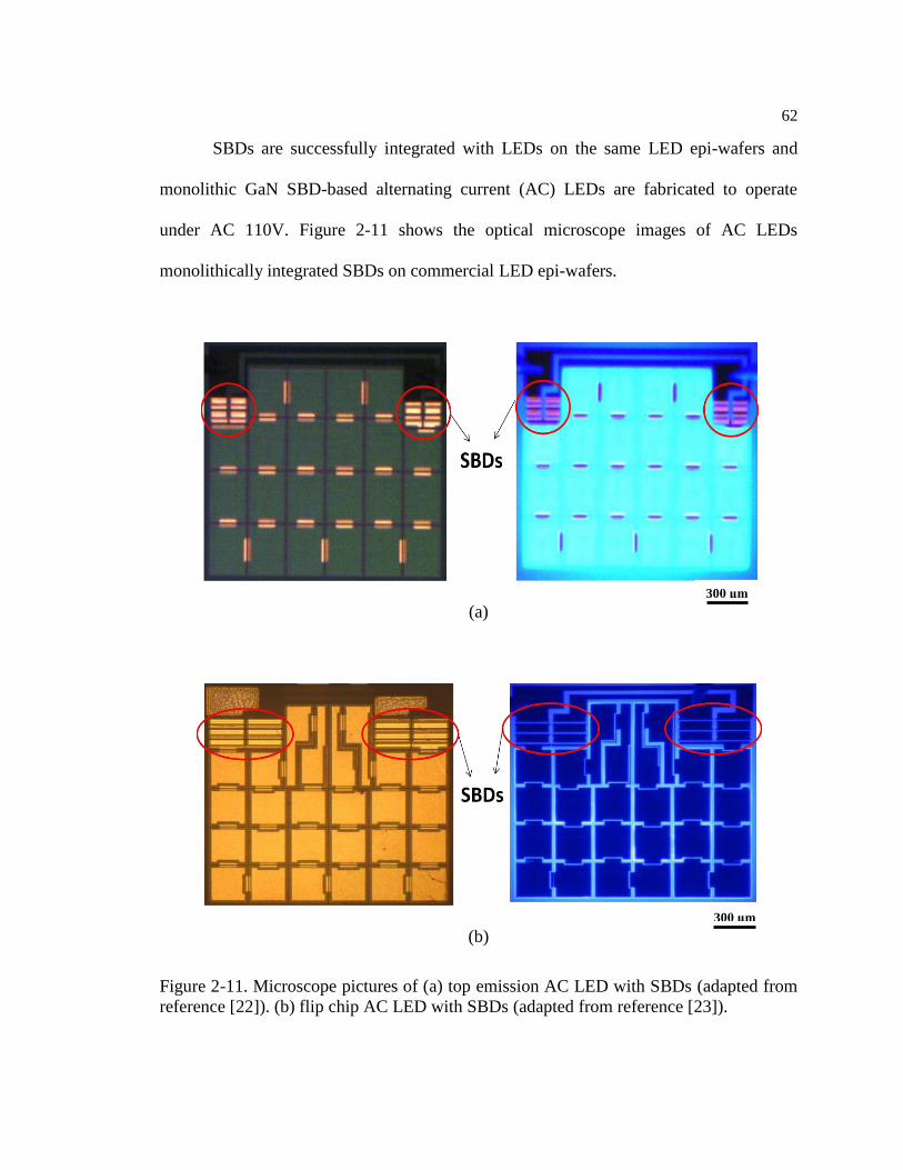
62
SBDs are successfully integrated with LEDs on the same LED epi-wafers and
monolithic GaN SBD-based alternating current (AC) LEDs are fabricated to operate
under AC 110V. Figure 2-11 shows the optical microscope images of AC LEDs
monolithically integrated SBDs on commercial LED epi-wafers.
(a)
(b)
Figure 2-11. Microscope pictures of (a) top emission AC LED with SBDs (adapted from
reference [22]). (b) flip chip AC LED with SBDs (adapted from reference [23]).
300 μm
300 μm
63
2.6 Conclusion
In summary, GaN SBDs with high breakdown voltage (>200V) and small on-state
voltage (~3.1 V at 100A/cm2) are successfully fabricated on GaN LED epi-wafers. The
effect of KOH with different solution concentration in remving the surface defects that
are induced by ICP etching process has been investigated. The results indicate that the
leakage current of SBDs is suppressed by four orders of magnitude after employing the
KOH solution with optimized concentration. Moreover, the defect density values by
leakage current mechanism analysis have been extracted. Lastly, the integration of GaN
LEDs and SBDs in the AC LED applications has been demonstrated.
64
Reference
1. W.-Y. Yeh, H.-H. Yen, Y.-J. Chan, The development of monolithic alternating
current light-emitting diode, (2011) 793910-793910.
2. Z. Li, J. Waldron, T. Detchprohm, C. Wetzel, R.F. Karlicek, T.P. Chow, Monolithic
integration of light-emitting diodes and power metal-oxide-semiconductor channel
high-electron-mobility transistors for light-emitting power integrated circuits in GaN
on sapphire substrate, Applied Physics Letters, 102 (2013).
3. Zhaojun Liu1, Jun Ma1, Tongde Huang1, Chao Liu1 and Kei May Lau, Selective
epitaxial growth of monolithically integrated GaN-based light emitting diodes with
AlGaN/GaN driving transistors,Appl. Phys. Lett. 104, 091103 (2014).
4. F.G. Kalaitzakis, E. Iliopoulos, c, G. Konstantinidis, N.T. Pelekanosa, Monolithic
integration of nitride-based transistor with Light Emitting Diode for sensing
applications, Microelectronic Engineering Volume 90, February 2012, Pages 33–36.
5. Hoshin H. Yee , H. F. Hong , and J. Y. Chang, “Improved surface characteristics of n-
GaN epitaxial structures after reactive ion etching”, Opt. Eng. 42(10), 2918-2922
(Oct 01, 2003).
6. Ho Won Jang and Jong-Lam Lee, Effect of Cl2 Plasma Treatment on Metal Contacts
to n-Type and p-Type GaN, J. Electrochem. Soc. 2003 150(9): G513-G519.
7. Fan, Qian, Chevtchenko, S., Ni, Xianfeng, Cho, Sang-Jun, Yun, Feng, and Morkoc,
Hadis, "Reactive ion etch damage on GaN and its recovery," Journal of Vacuum
Science & Technology B: Microelectronics and Nanometer Structures, Volume 24,
Issue 3, May 2006, Page(s):1197 - 1201.
65
8. P. B. Shah1, I. Batyrev, M. A. Derenge, U. Lee, C. Nyguen and K. A. Jones,
"Schottky metal-GaN interface KOH pretreatment for improved device performance,"
J. Vac. Sci. Technol. A 28, 684 (2010).
9. Ho Gyoung Kim, Sang Ho Kim, Parijat Deb, Tim Sands, "Effect of KOH treatment
on the schottky barrier height and reverse leakage current in Pt/n-GaN," Journal of
Electronic Materials 2006, Volume 35, Issue 1, pp 107-112.
10. J. Spradlin, S. Dogan1, M. Mikkelson, D. Huang, L. He1, D. Johnstone, H. Morkoç
and R. J. Molnar, "Improvement of n-GaN Schottky diode rectifying characteristics
using KOH etching," Appl. Phys. Lett. 82, 3556 (2003).
11. Hogyoung Kim, Effect of KOH treatment on the Schottky barrier inhomogeneity in
Ni/n-GaN, Materials Science in Semiconductor Processing Volume 13, Issue 1,
February 2010, Pages 51–55.
12. Kyoung Jin Choi, Ho Wan Jang and Jong-Lam Lee, "Observation of inductively
coupled-plasma-induced damage on n-type GaN using deep-level transient
spectroscopy," Appl. Phys. Lett. 82, 1233 (2003).
13. E Harush, S Brandon, J Salzman and Y Paz1, "The effect of mass transfer on the
photoelectrochemical etching of GaN," 2002 Semicond. Sci. Technol. 17 510.
14. J. Spradlin, S. Dogan, M. Mikkelson, D. Huang, L. He1, D. Johnstone, H. Morkoç
and R. J. Molnar, "Improvement of n-GaN Schottky diode rectifying characteristics
using KOH etching," Appl. Phys. Lett. 82, 3556 (2003).
15. Dieter K. Schroder, Semiconductor Material and Device Characterization, 3rd
Edition,January 2006, Wiley-IEEE Press.
66
16. H. Hasegawa, T. Inagaki, S. Ootomo, and T. Hashizume, Mechanisms of current
collapse and gate leakage currents in AlGaNÕGaN heterostructure field effect
transistors J. Vac. Sci. Technol. B 21, 1844 -1855.
17. Tamotsu Hashizume, Junji Kotani and Hideki Hasegawa, "Leakage mechanism in
GaN and AlGaN Schottky interfaces," Appl. Phys. Lett. 84, 4884 (2004).
18. C.Y. Chang and S.M. Sze, “CARRIER TRANSPORT ACROSS METAL-
SEMICONDUCTOR BARRIERS”, Solid-State Electronics, Volume 13, Issue 6, June
1970, Pages 727–740.
19. Wei Lu, Lingquan Wang, Siyuan Gu, David P. R. Aplin, Daniel M. Estrada, Paul K.
L. Yu, and Peter M. Asbeck,"Analysis of Reverse Leakage Current and Breakdown
Voltage in GaN and InGaN/GaN Schottky Barriers," IEEE TRANSACTIONS ON
ELECTRON DEVICES, VOL. 58, NO. 7, JULY 2011.
20. Junji Kotani, , Hideki Hasegawa, Tamotsu Hashizume ,"Computer simulation of
current transport in GaN and AlGaN Schottky diodes based on thin surface barrier
model," Applied Surface Science Volume 237, Issues 1–4, 15 October 2004, Pages
213–218.
21. S. J. Chang, C. H. Chen, Y. K. Su, J. K. Sheu, W. C. Lai, J. M. Tsai, C. H. Liu, and S.
C. Chen, "Improved ESD Protection by Combining InGaN–GaN MQW LEDs With
GaN Schottky Diodes," IEEE ELECTRON DEVICE LETTERS, VOL. 24, NO. 3,
MAR. 2003.
22. Jie Liu, COLLOIDAL QUANTUM DOT-ENABLING AND ALTERNATING
CURRENT DRIVEN GALLIUM NITRIDE BASED LIGHT EMITTING DIODE
TECHNOLOGY, the Pennsylvania State University, 2013.
67
23. Zhenyu Jiang, LIGHT EMITTING DIODES AND PHOTODETECTORS BASED
ON III-NITRIDE AND COLLOIDAL QUANTUM DOT MATERIALS, the
Pennsylvania State University, 2014.
68
Chapter 3
A study of the conductive interface region between gallium nitride and
patterned sapphire substrate
In Chapter 2, GaN SBDs with high voltage blocking capability and low on-state
voltage which are fabricated on commercial LED epi-wafers have been demonstrated.
The average forward voltage Vf at the current of 100 A/cm2 is 1.6 V, and the leakage
current is lower than 10 mA/cm2 at 100V reverse voltage. The study in Chapter 2 have
revealed that the leakage current is reduced by applying the mixed etching process to
decrease the damaged surface region, while this study aims to understand the mechanism
under the low on-state voltage in SBDs.
3.1 Introduction
The technology of Gallium nitride (GaN)-based devices system has earned a
significant place in optical and electronic applications for decades. Recently, the interests
in monolithic integration of GaN optical devices and power electronic devices is
growing, and monolithically integrated GaN-based light emitting diodes (LEDs) with
schottky barrier diodes (SBDs) or high electron mobility transistors (HEMTs) have been
demonstrated and proposed for AC-LEDs, smart light communication system, sensing,
and other applications [1-4]. In a monolithic LED system, the dissipated power of power
electronic devices should be minimized to improve the efficiency of the whole LED
system, hence low-voltage bias is highly desirable when running the power electronic
devices that are integrated on LED epi-wafers.
69
Traditionally, single polished flat sapphire substrate (FSS) is the most commonly
used substrate for GaN heteroepitaxial growth [5]. However, GaN LEDs on FSS have a
low light extraction efficiency [6]. Recently, patterned sapphire substrates (PSS) have
been applied to the epi-layer growth GaN LEDs to increase the light extraction efficiency
[7]. It is well known that a significant number of threading dislocations can be observed
in the interfacial region due to the lattice mismatches between GaN and sapphire [8].
These dislocations decorated by impurities can form a highly conductive current path and
potentially affect the lateral current transport in the fabricated devices [9]. Compared
with the GaN and FSS interface, a higher dislocation density has been observed in the
GaN and PSS interface due to the involvement of separated GaN islands at the initial
epitaxial growth stage [10]. Thus, it is envisioned that the interface region between GaN
epilayer and PSS is expected to have much higher conductance than flat sapphire
substrate due to the rough patterned interface.
In this work, we show by comparing the current-voltage characteristics of the
GaN films grown on PSS and FSS that the conductance of the interface region in PSS
samples is higher than that in FSS, and suggest that the carriers in the GaN and sapphire
interface region are oxygen or nitrogen vacancies by calculating the dopant ionization
energies. A two-layer model is used to quantify the donor concentration. Furthermore, the
performance of GaN schottky diodes with different donor concentration in the interface
region is investigated by Sentaurus TCAD tools. Finally, schottky diodes with low on-
state voltages, low leakage currents, and high breakdown voltages are successfully
fabricated on commercial GaN LED epi-wafers with PSS.
70
3.2 Experimental
Unintentionally doped GaN films (Nd < 1×10¹⁷
cm-3
) with the thickness around
2um were grown by one run on PSS and on FSS in a metal organic chemical vapor
deposition (MOCVD) system. The sapphire patterns have the dome shape with height of
1.5 um and bottom diameter of 2.5 um. Rectangular transfer length measurement (TLM)
patterns, consisting of six 80um ×250um contacts with spacing of 4, 8, 12, 16, 20um,
were fabricated.
SBDs are fabricated on 2-inch commercial GaN LED PSS epi-wafers. The
epitaxial structure comprises by a 200 nm p-type GaN layer, a 50nm multiple quantum
well (MQW) layer, a 2.4 um n-type GaN layer and a 2.5 um unintentionally doped GaN
layer. The fabricated SBDs have a mesa structure formed by Cl2/Ar (20sccm/5sccm)
inductively coupled plasma cyclic etching (650W source power, 50W rf chuck power).
After the etching process, the samples were immersed in KOH solution to remove ICP
induced surface defects. Schottky contacts with the contact area of 2.5×10⁻⁵
cm-2
are
formed by the deposition of Ni/Al/Ti/Au (50nm/500nm/100nm/200nm) and ohmic
contacts were formed by Ti/Al/Ti/Au (10nm/40nm/40nm/200nm). The contact metals
were deposited by liftoff e-beam evaporation and annealed at 700oC for 2min under N2
ambient.
I-V characteristics were measured by Keithley 2612 source meter. A low-
temperature probe station system (including a DE-204 probes from Advanced Research
Systems, an ARS-4HW water-cooled helium compressor from Advanced Research
Systems, and a 336 temperature controller from Lake Shore) were used for the
71
temperature-dependent measurement. The numerical analysis of GaN SBDs with the
existence of a parallel current path at the bottom of the GaN in the present study was
performed with Synopsys TCAD tools.
3.3 Results and Discussion
Figure 3-1 shows the resistance measurement results in varying temperatures.
Four-point resistance between two ohmic contacts with the distance of 400um on both
PSS and FSS samples are measured from 290k to 70k. The contact resistances were
removed from the total resistances by transmission line method (TLM) measurements. It
can be concluded from the ln(R)-T curves that the conductance of PSS samples is more
than 5times than the one of FSS sample at room temperature, implying higher on-state
current can be obtained on PSS samples.
In this study, based on the relationship between the resistance R and the carrier
activation energy ΔE at low temperature [11],
0( ) exp( )2
ER T R
kT
(1)
, we obtained the donor activation energies, which were 30meV and 29meV for PSS and
FSS samples respectively, from the slope of the ln(R)-T curve as shown in Fig. 3-1. Since
the ionization energies of both oxygen and nitrogen vacancies are reported as 29meV
[12], 29.3meV [11], and 30meV [13], our results suggest that oxygen and/or nitrogen
vacancies are the possible physical origin of the GaN and sapphire interface carriers.
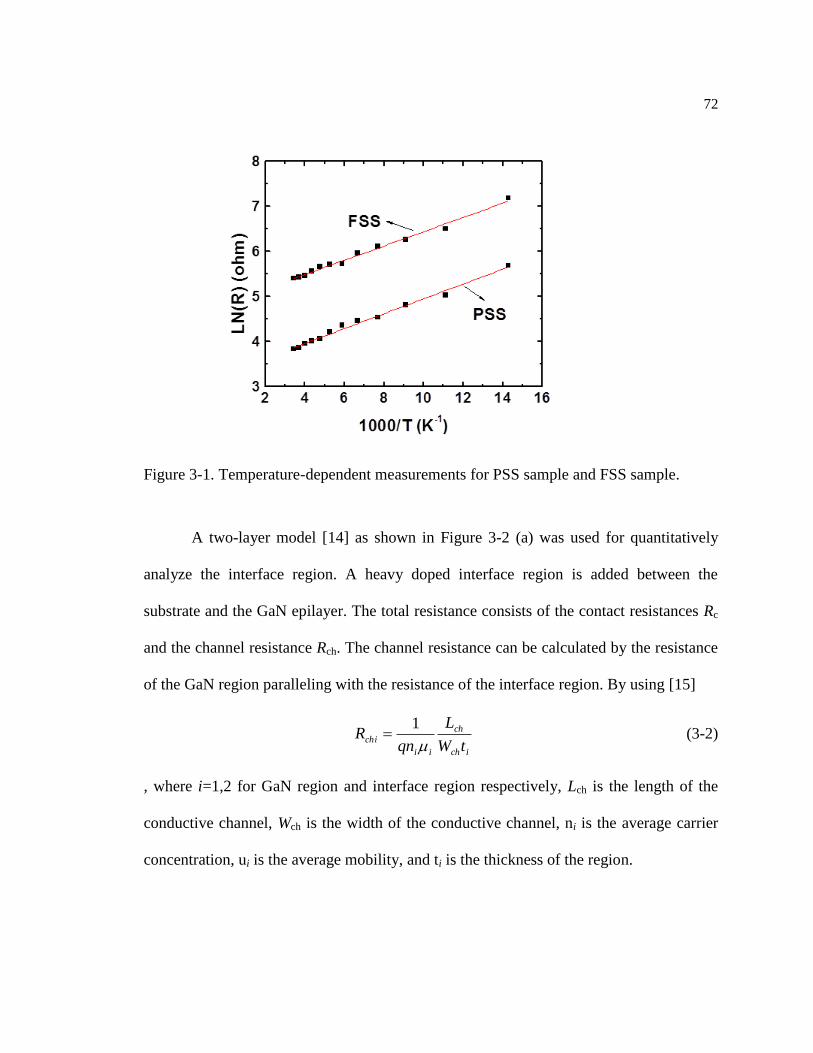
72
Figure 3-1. Temperature-dependent measurements for PSS sample and FSS sample.
A two-layer model [14] as shown in Figure 3-2 (a) was used for quantitatively
analyze the interface region. A heavy doped interface region is added between the
substrate and the GaN epilayer. The total resistance consists of the contact resistances Rc
and the channel resistance Rch. The channel resistance can be calculated by the resistance
of the GaN region paralleling with the resistance of the interface region. By using [15]
ich
ch
ii
chitW
L
qnR
1 (3-2)
, where i=1,2 for GaN region and interface region respectively, Lch is the length of the
conductive channel, Wch is the width of the conductive channel, ni is the average carrier
concentration, ui is the average mobility, and ti is the thickness of the region.
73
RcRc
Rch1
Rch2
Lch t1
t2
Wch
Sapphire
Interface
GaN
(a)
(b)
Figure 3-2. (a) Schematic of series resistances between two ohmic contacts on a GaN
film. (b) Typical measured I-V characteristics between two ohmic contacts with the
distance of 400um on the GaN samples with PSS and FSS respectively.
Figure 3-2(b) shows the typical I-V characteristics between two ohmic contacts
with the distance of 400um on the GaN samples with PSS and FSS respectively. After
74
subtracting the contact resistances, the channel resistance Rch=75 ohm for PSS-based
samples and Rch=410 ohm for FSS-based samples were obtained. In both PSS and FSS
samples, Lch =400 um, Wch =230 um, other parameters can be extracted from the curve
fitting by incorporating the condition of t1+t2=2 um and 0 um ≤ t2 ≤ 0.7 um [11] and using
the GaN doping dependence model [16]
171021
94555
i
i n (3-3)
, good fittings for IV curves of ohmic contacts with different spaces on PSS samples were
achieved using following parameters t1=1.5um, t2=0.5um, n1=3×10¹⁶
cm-3
, n2=1×10²⁰
cm-3
.
The parameters for FSS samples are t1=1.5um, t2=0.5um, n1=3×10¹⁶
cm-3
, n2=8×10¹⁸
cm-3
.
The increase of the carrier concentration in PSS samples could be explained by the rough
interface which has a larger contact area for GaN epilayers and sapphire, increasing the
number and the possibility of the oxygen atoms diffusing from the substrate.
Simulation models are built to investigate the influence of the carrier
concentration in the interface region on the behavior of GaN schottky diodes. The device
model consists by an 1.5 um-thick GaN film with the conductivity of 4Ω-1
cm-1
and a 0.5
um-thick interface layer with alterable conductivity. The schottky barrier height is set to
be 1 eV for Ni/GaN metal contact [17]. The doping density in ohmic contact is 1×10²⁰
cm-3
. Figure 3-3 shows the simulated I-V characteristics of GaN schottky diodes with
three different conductivities in the interface region. The results confirm that the
conductive interface region could benefit the on-state characteristics of schottky rectifiers
without deteriorating their performance under reverse biases.
75
Figure 3-3. Simulated forward I-V characteristics of GaN schottky diodes with three
different conductivities in the interface region. The inset is the reverse I-V curves.
Figure 3-4 shows typical three I-V curves of the SBDs fabricated on GaN LED
epi-wafers with PSS. The average forward voltage Vf at the current of 20 mA is 1.2 V,
corresponding to a low dissipated power integrated in a system. Meanwhile, the leakage
current keeps below 1uA at the reverse bias of 100V and does not exceed -100uA at -
150V. With the absence of interface region, the calculated on-state forward current (the
dash line) is much lower than our experimental results, suggesting that the high forward
currents in our fabricated SBDs should attributed to the highly conductive GaN and
sapphire interface region.
76
Figure 3-4. Measured I-V curves of the SBDs fabricated on GaN LED wafers with PSS.
The inset is the structure of the SBDs.
3.4 Conclusion
We confirm that the conductance of the interface region in PSS sample is higher
than in FSS. A two-layer model is used to quantify the interface conductivity.
Furthermore, the performance of GaN schottky diodes with different conductivity in the
interface region is investigated by Sentaurus TCAD tools. Finally, schottky diodes with
low on-state voltage, low leakage current, and high breakdown voltage are demonstrated
by fabricating on commercial GaN LED wafers with PSS.
77
Reference
1. W.-Y. Yeh, H.-H. Yen, Y.-J. Chan, The development of monolithic alternating
current light-emitting diode, (2011) 793910-793910.
2. Z. Li, J. Waldron, T. Detchprohm, C. Wetzel, R.F. Karlicek, T.P. Chow, Monolithic
integration of light-emitting diodes and power metal-oxide-semiconductor channel
high-electron-mobility transistors for light-emitting power integrated circuits in GaN
on sapphire substrate, Applied Physics Letters, 102 (2013).
3. Zhaojun Liu1, Jun Ma1, Tongde Huang1, Chao Liu1 and Kei May Lau, Selective
epitaxial growth of monolithically integrated GaN-based light emitting diodes with
AlGaN/GaN driving transistors,Appl. Phys. Lett. 104, 091103 (2014).
4. F.G. Kalaitzakis, E. Iliopoulos, c, G. Konstantinidis, N.T. Pelekanosa, Monolithic
integration of nitride-based transistor with Light Emitting Diode for sensing
applications, Microelectronic Engineering Volume 90, February 2012, Pages 33–36.
5. C.I.H. Ashby, C.C. Mitchell, J. Han, N.A. Missert, P.P. Provencio, D.M.
Follstaedt,G.M. Peake, L. Griego, Appl. Phys. Lett. 77 (2000) 3233.
6. Xiao-Hui Huang, Jian-Ping Liu, Ya-Ying Fan, Jun-Jie Kong, Hui Yang, and Huai-
Bing Wang,Effect of Patterned Sapphire Substrate Shape on Light Output Power of
GaN-Based LEDs, IEEE PHOTONICS TECHNOLOGY LETTERS, VOL. 23, NO.
14, JULY 15, 2011.
7. Hyoungwon Park, Kyeong-Jae Byeon, Jong-Jin Jang, Okhyun Nam, Heon Lee,
Enhancement of photo- and electro-luminescence of GaN-based LED structure grown
78
on a nanometer-scaled patterned sapphire substrate, Volume 88, Issue 11, November
2011, Pages 3207–3213.
8. Hui-Youn Shin, Y. I. Chang, S. K. Kwon, K. T. Lee, M. J. Cho and K. H. Park The
Growth Characteristics of a GaN Layer on a Cone-Shaped Patterned Sapphire
Substrate by TEM Observation, Journal of the Korean Physical Society, Vol. 50, No.
4, April 2007, pp. 1147∼1151.
9. Sun, X.L., Goss, S.H., Brillson, L.J., Look, D.C., Molnar, R.J., Depth-dependent
investigation of defects and impurity doping in GaN/sapphire using scanning electron
microscopy and cathodoluminescence spectroscopy, JOURNAL OF APPLIED
PHYSICS VOLUME 91, NUMBER 10 15 MAY 2002.
10. Tae Su Oh, Hyun Jeong, Yong Seok Lee, Tae Hoon Seo, Ah Hyun Park, Hun Kim,
Kang Jea Lee, Mun Seok Jeong c, Eun-Kyung Suh, Defect structure originating from
threading dislocations within the GaN film grown on a convex patterned sapphire
substrate , Thin Solid Films 519 (2011) 2398–2401.
11. Abhishek Motayed,Albert V. Davydov, S. N. Mohammad, and John Melngailis,
Experimental investigation of electron transport properties of gallium nitride
nanowires, JOURNAL OF APPLIED PHYSICS 104, 024302 2008.
12. J. Zolper, R. G. Wilson, S. J. Pearton, and R. A. Stall, Appl. Phys. Lett.68, 1945,
1996.
13. M. E. Levinshtein, S. L. Rumyantsev, and M. S. Shur, Properties of Advanced
Semiconductor Materials: GaN, AlN, InN, BN, SiC, SiGe Wiley, New York, USA,
2001, p. 8.
79
14. B.J. Anscll, I,. Harrison, C.T. Foxon, .I.J. Harris and T.S. Cheng, Direct evidence for
defect conduction at interface between gallium nitride and sapphire, ELECTRONICS
LETTERS 6th July2000 Vol. 36 No. 14.
15. Dieter K. Schroder, Semiconductor Material and Device Characterization, John Wiley
& Sons, Feb 10, 2006.
16. Tigran T. Mnatsakanov, Michael E. Levinshtein, Lubov I. Pomortseva, Sergey N.
Yurkov, Grigory S. Simin, M. Asif Khan, Carrier mobility model for GaN, Solid-
State Electronics 47 (2003) 111–115.
17. A C Schmitzy, A T Pingy, M Asif Khanz, Q Chenz, J W Yangz, and I Adesida:
Schottky barrier properties of various metals on n-type GaN. Semiconductor Science
Technology 11, 1464 (1996).
Chapter 4
Investigation of drain current saturation feature in AlGaN/GaN high electron
mobility transistors
In this chapter, gate bias dependence of drain current saturation in AlGaN/GaN
HEMTs was studied. A series resistance model was used to explain this saturation and
device simulations were carried out to confirm the explaination. As gate bias increases,
the drain current of AlGaN/GaN HEMTs tends to be saturated. In addition, the drain
current of the devices with shorter gate length saturates more quickly than the devices
with longer gate length. The influence of this saturation feature on the transconductance
and the extracted value of electron mobility was also analyzed. Moreover, we evaluated
the possibility of using AlGaN/GaN HEMTs in logic inverter applications based on the
saturation feature.
4.1 Introduction
Recently, GaN-based HEMTs have been studied substantially as promising
candidates in high-power microwave applications [1-3]. The static behavior of a
transistor could be evaluated by its DC output and transfer characteristics. Some crucial
parameters including transconductance and low field electron mobility could be extracted
from transfer characteristics to evaluate the device performance. It is shown in our own
measurement results of GaN-based HEMTs and also reported in other studies [3, 4] that
the drain current has a tendency of saturation in the case of gate bias larger than threshold
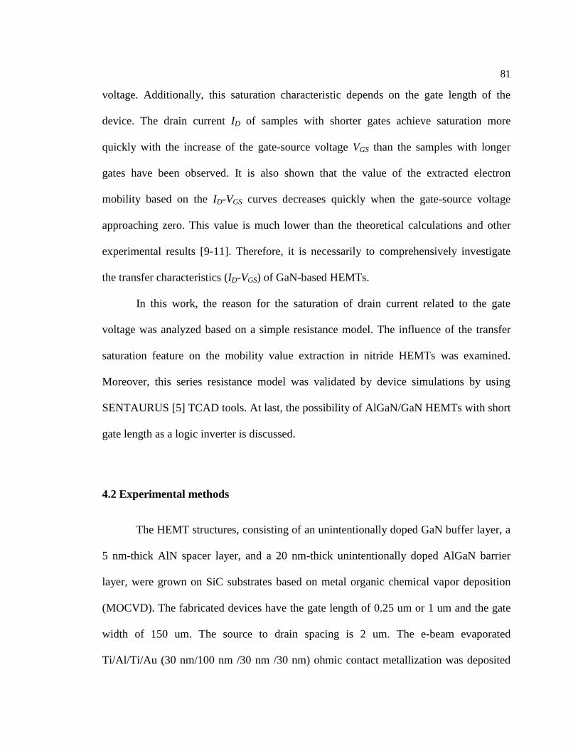
81
voltage. Additionally, this saturation characteristic depends on the gate length of the
device. The drain current ID of samples with shorter gates achieve saturation more
quickly with the increase of the gate-source voltage VGS than the samples with longer
gates have been observed. It is also shown that the value of the extracted electron
mobility based on the ID-VGS curves decreases quickly when the gate-source voltage
approaching zero. This value is much lower than the theoretical calculations and other
experimental results [9-11]. Therefore, it is necessarily to comprehensively investigate
the transfer characteristics (ID-VGS) of GaN-based HEMTs.
In this work, the reason for the saturation of drain current related to the gate
voltage was analyzed based on a simple resistance model. The influence of the transfer
saturation feature on the mobility value extraction in nitride HEMTs was examined.
Moreover, this series resistance model was validated by device simulations by using
SENTAURUS [5] TCAD tools. At last, the possibility of AlGaN/GaN HEMTs with short
gate length as a logic inverter is discussed.
4.2 Experimental methods
The HEMT structures, consisting of an unintentionally doped GaN buffer layer, a
5 nm-thick AlN spacer layer, and a 20 nm-thick unintentionally doped AlGaN barrier
layer, were grown on SiC substrates based on metal organic chemical vapor deposition
(MOCVD). The fabricated devices have the gate length of 0.25 um or 1 um and the gate
width of 150 um. The source to drain spacing is 2 um. The e-beam evaporated
Ti/Al/Ti/Au (30 nm/100 nm /30 nm /30 nm) ohmic contact metallization was deposited
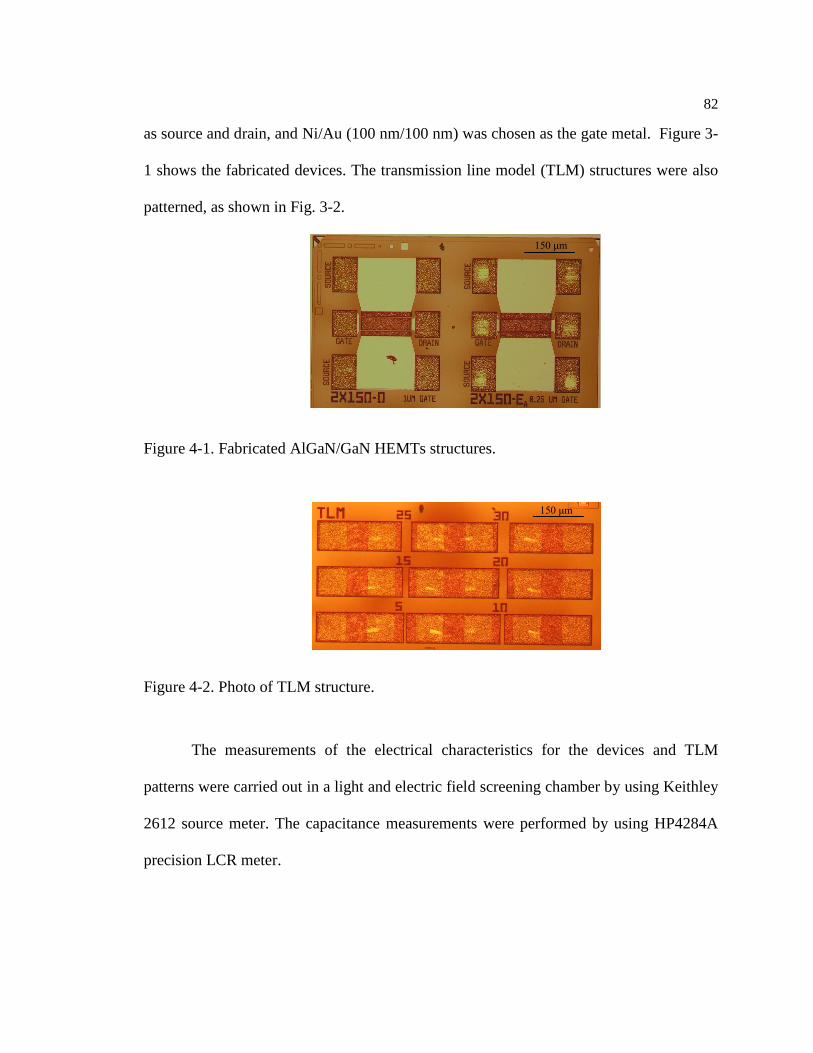
82
as source and drain, and Ni/Au (100 nm/100 nm) was chosen as the gate metal. Figure 3-
1 shows the fabricated devices. The transmission line model (TLM) structures were also
patterned, as shown in Fig. 3-2.
Figure 4-1. Fabricated AlGaN/GaN HEMTs structures.
Figure 4-2. Photo of TLM structure.
The measurements of the electrical characteristics for the devices and TLM
patterns were carried out in a light and electric field screening chamber by using Keithley
2612 source meter. The capacitance measurements were performed by using HP4284A
precision LCR meter.
150 μm
150 μm
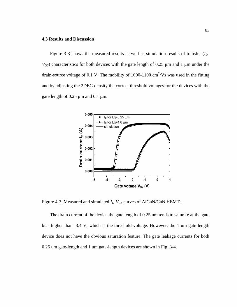
83
4.3 Results and Discussion
Figure 3-3 shows the measured results as well as simulation results of transfer (ID-
VGS) characteristics for both devices with the gate length of 0.25 μm and 1 μm under the
drain-source voltage of 0.1 V. The mobility of 1000-1100 cm2/Vs was used in the fitting
and by adjusting the 2DEG density the correct threshold voltages for the devices with the
gate length of 0.25 μm and 0.1 μm.
-5 -4 -3 -2 -1 0 1
0.000
0.001
0.002
0.003
0.004
0.005
Dra
in c
urr
en
t I D
(A
)
Gate votage VGS (V)
ID for Lg=0.25 m
ID for Lg=1.0 m
simulation
Figure 4-3. Measured and simulated ID-VGS curves of AlGaN/GaN HEMTs.
The drain current of the device the gate length of 0.25 um tends to saturate at the gate
bias higher than -3.4 V, which is the threshold voltage. However, the 1 um gate-length
device does not have the obvious saturation feature. The gate leakage currents for both
0.25 um gate-length and 1 um gate-length devices are shown in Fig. 3-4.
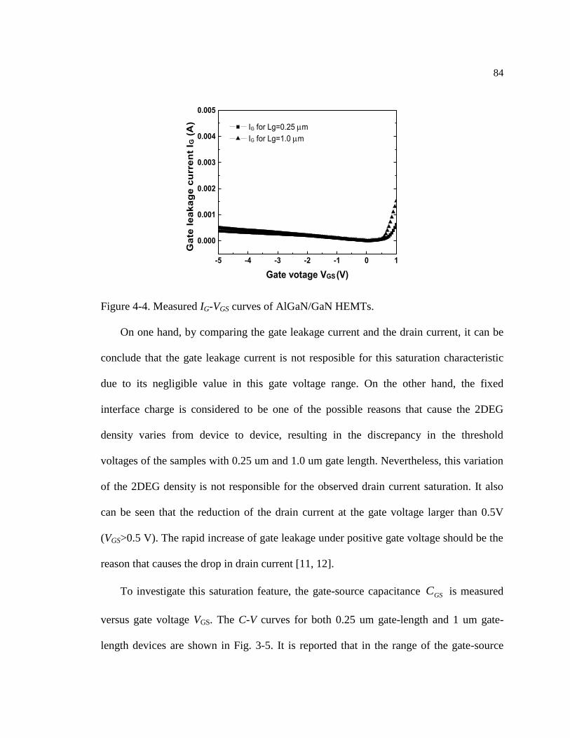
84
-5 -4 -3 -2 -1 0 1
0.000
0.001
0.002
0.003
0.004
0.005
Ga
te l
ea
ka
ge
cu
rre
nt
I G (
A)
Gate votage VGS (V)
IG for Lg=0.25 m
IG for Lg=1.0 m
Figure 4-4. Measured IG-VGS curves of AlGaN/GaN HEMTs.
On one hand, by comparing the gate leakage current and the drain current, it can be
conclude that the gate leakage current is not resposible for this saturation characteristic
due to its negligible value in this gate voltage range. On the other hand, the fixed
interface charge is considered to be one of the possible reasons that cause the 2DEG
density varies from device to device, resulting in the discrepancy in the threshold
voltages of the samples with 0.25 um and 1.0 um gate length. Nevertheless, this variation
of the 2DEG density is not responsible for the observed drain current saturation. It also
can be seen that the reduction of the drain current at the gate voltage larger than 0.5V
(VGS>0.5 V). The rapid increase of gate leakage under positive gate voltage should be the
reason that causes the drop in drain current [11, 12].
To investigate this saturation feature, the gate-source capacitance GSC is measured
versus gate voltage VGS. The C-V curves for both 0.25 um gate-length and 1 um gate-
length devices are shown in Fig. 3-5. It is reported that in the range of the gate-source
85
voltage GSV within which the gate-source capacitance is almost independent of the gate-
source voltage, the channel 2DEG density chn can be described as [6]
)( thGSGS
ch VVq
Cn (3-1)
where Vth is the threshold voltage, q is the electron charge, and CGS is the gate-source
capacitance. Then, the channel electron mobility ch could be extracted from
Wqn
LG
ch
gch
ch (3-2)
, where Lg is the gate length, W is the gate width, Gch is the channel conductance. The
electron mobility versus the 2DEG sheet density for the 0.25 um gate-length sample is
shown in Fig. 3-6. This mobility value is significant lower than the values obtained from
Hall measurements and gated TLM measurements. This inconsistency is not in agreement
with theoretical predictions and other measurement results [8-10].
-4 -3 -2 -1 0
0.0
1.0x10⁻⁷
2.0x10⁻⁷
3.0x10⁻⁷
4.0x10⁻⁷
Lg=1 m
Lg=0.25 m
CG
S (
F/c
m2)
VGS (V)
Figure 4-5. Gate-source capacitance as the function of gate voltage.
86
Figure 4-6. The electron mobility versus 2DEG density for the 0.25 um gate-length
sample.
The saturation transfer characteristics are investigated using a resistance model to
explain the saturation feature in this section.
The channel current (Ich) under the gate can be given by
chchch vqnI (3-3)
, where vch is the electron velocity. Under VDS = 0.1 V, the lateral electric filed (E) in
channel under the gate region is far below the value that induce the electron velocity
saturation, which is ~200 kV/cm [13]. Therefore, in this linear region the electron
velocity should be proportional to the lateral electric field E in channel, given by
vch=μchE (3-4)
. Then, the drain current Ids is
chchDS qnI (3-5)
5.00E+012 1.00E+013
500
1000
Mo
bility (
cm
2/V
s)
2DEG density (cm-2)
87
Figure 4-7. Illustration of the series resistance in a GaN HEMT.
In the Fig. 3-7, Vch repsents the channel voltage and E repsents the channel lateral electric
field. Lg, Lsg, and Ldg represent the gate length, source to gate space and drain to gate
space respectively. Rc, Rs, Rd and Rch are the contact resistance, source to gate resistance,
drain to gate resistance, and channel resistance respectively.
The voltage drop Vch along the channel can be expressed as
2
chch DS
c s d ch
RV V
R R R R
(3-6)
, where Rc is the contact resistance, Rch is the channel resistance, Rs is the source-gate
resistance, and Rd is the drain-gate resistance. Therefore, the lateral electric field E can be
calculated by the channel voltage drop Vch and gate length Lg as
g
ch
L
V (3-7)
AlGaNS G D
RC RSRch RD
RC
Lsg Ldg
E
Vch
GaN
Lg
88
The source-gate resistance Rs, drain-gate resistance Rd, and channel resistance Rch
can be given respectively by
0 0
sg
s
LR
qn (3-8)
0 0
dg
d
LR
qn (3-9)
and
g
ch
ch ch
LR
qn (3-10)
, where Lsg is the source-gate space, Ldg is the drain-gate space, n0 is the 2DEG density at
zero gate voltage, and 0 is the electron mobility at zero gate voltage. Usually, the
partially depleted region under the gate caused by the schottky contact of gate makes the
channel 2DEG density nch a little smaller than the 2DEG density at zero gate voltage n0.
Using the equations (3-5) – (3-10), the drain current can be expressed as
0 0
1
21
DSDS
gs d c
s d sg gd ch ch
VI
LR R R n
R R L L n
(3-11)
Given that the mobility is not influence by gate bias, the ratio of 0 0
ch ch
n
n
in equation (7)
will reduce to unity when the gate voltage VGS increases. Therefore, the term of
0 0g
sg gd ch ch
L n
L L n
could be neglected in the case of
g
sg gd
L
L L<<1. This confirms that the
variation of 2DEG density cannot influence the saturation characteristics of drain current,
even though this variation can lead to the difference in the threshold voltages in
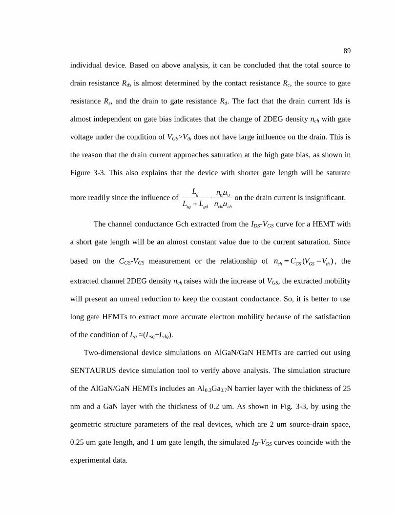
89
individual device. Based on above analysis, it can be concluded that the total source to
drain resistance Rds is almost determined by the contact resistance Rc, the source to gate
resistance Rs, and the drain to gate resistance Rd. The fact that the drain current Ids is
almost independent on gate bias indicates that the change of 2DEG density nch with gate
voltage under the condition of VGS>Vth does not have large influence on the drain. This is
the reason that the drain current approaches saturation at the high gate bias, as shown in
Figure 3-3. This also explains that the device with shorter gate length will be saturate
more readily since the influence of 0 0g
sg gd ch ch
L n
L L n
on the drain current is insignificant.
The channel conductance Gch extracted from the IDS-VGS curve for a HEMT with
a short gate length will be an almost constant value due to the current saturation. Since
based on the CGS-VGS measurement or the relationship of ( )ch GS GS thn C V V , the
extracted channel 2DEG density nch raises with the increase of VGS, the extracted mobility
will present an unreal reduction to keep the constant conductance. So, it is better to use
long gate HEMTs to extract more accurate electron mobility because of the satisfaction
of the condition of Lg ≈(Lsg+Ldg).
Two-dimensional device simulations on AlGaN/GaN HEMTs are carried out using
SENTAURUS device simulation tool to verify above analysis. The simulation structure
of the AlGaN/GaN HEMTs includes an Al0.3Ga0.7N barrier layer with the thickness of 25
nm and a GaN layer with the thickness of 0.2 um. As shown in Fig. 3-3, by using the
geometric structure parameters of the real devices, which are 2 um source-drain space,
0.25 um gate length, and 1 um gate length, the simulated ID-VGS curves coincide with the
experimental data.
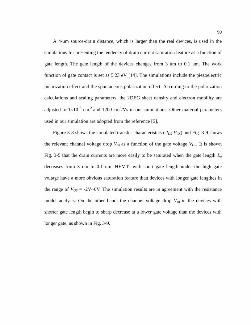
90
A 4-um source-drain distance, which is larger than the real devices, is used in the
simulations for presenting the tendency of drain current saturation feature as a function of
gate length. The gate length of the devices changes from 3 um to 0.1 um. The work
function of gate contact is set as 5.23 eV [14]. The simulations include the piezoelectric
polarization effect and the spontaneous polarization effect. According to the polarization
calculations and scaling parameters, the 2DEG sheet density and electron mobility are
adjusted to 11013
cm-2
and 1200 cm2/Vs in our simulations. Other material parameters
used in our simulation are adopted from the reference [5].
Figure 3-8 shows the simulated transfer characteristics ( IDS-VGS) and Fig. 3-9 shows
the relevant channel voltage drop Vch as a function of the gate voltage VGS. It is shown
Fig. 3-5 that the drain currents are more easily to be saturated when the gate length Lg
decreases from 3 um to 0.1 um. HEMTs with short gate length under the high gate
voltage have a more obvious saturation feature than devices with longer gate lengthes in
the range of VGS = -2V~0V. The simulation results are in agreement with the resistance
model analysis. On the other hand, the channel voltage drop Vch in the devices with
shorter gate length begin to sharp decrease at a lower gate voltage than the devices with
longer gate, as shown in Fig. 3-9.
91
-4 -3 -2 -1 00.00
0.01
0.02
0.03
0.04
0.05
I D (
A/m
m)
Gate voltage VGS (V)
Gate length Lg
0.1m
0.4m
0.7m
1.0m
2.0m
3.0m
Figure 4-8. The drain current IDS as a function of gate voltage VGS at VDS=0.1 V with
different gate length.
-4 -3 -2 -1 00.00
0.02
0.04
0.06
0.08
0.10
Gate length Lg
0.1um
0.4um
0.7um
1.0um
2.0um
3.0um
Vc
h (
V)
Gate voltage VGS (V)
Figure 4-9. The channel voltage drop Vch as a function of gate voltage VGS at VDS=0.1 V
with different gate length.
92
HEMTs with short gate length can be used for logic inverters due to the saturation
characteristic of IDS-VGS. It is shown in Fig. 3-9 that the channel voltage drop Vch is in
inverse relation with the gate voltage VGS. Therefore, inverters based on HEMTs can be
realized by using the gate voltage VGS as input signal and the channel voltage drop Vch as
output signal. Additional ohmic contacts can be used as the output signal electrodes and
they can be placed closely on each side of the gate contact to form a single HEMT invert.
HEMT-based inverters are especially valuable to fabricate logic inverters on InAs
substrate, since it is difficult to form pMOSFETs on InAs substrate. Notwithstanding, in
the future it is still necessary and very important to study carefully the transient character
and its influence on the proposed HEMT-based inverters.
4.4 Conclusion
In conclusion, this chapter investigated the gate length dependence of transfer
characteristics for GaN HEMTs. The drain currents become saturation when the gate bias
accesses to zero. A simple series resistance model was proposed to explain this saturation
feature. The analysis concludes that the contact resistance Rc, the source to gate resistance
Rs, and the drain to gate resistance Rd are the primary contributions to the total source to
drain resistance Rds when the gate bias accesses to zero. Therefore, the drain current in
GaN HEMTs with short gate length do not depend on the gate bias. Large error will take
place when electron mobility is extracted from the saturation region of IDS-VGS
characteristics. At last, logic inverters based GaN HEMTs with ultra short gate length can
be realized by utilizing the saturation feature.
93
Reference
1. U. K. Mishra, L. Shen, T. E.Kazior, and Y.-F.Wu, “GaN-based RF power devices and
amplifiers”, Proc. IEEE 96, 287 (2008).
2. W. Saito, T. Nitta, Y. Kakiuchi, Y. Saito, K. Tsuda, I. Omura, and M. Yamaguchi, “A
120-W boost converter operation using a high-voltage GaN-HEMT,” IEEE Electron
Device Lett. 29, 8 (2008).
3. J. Yang, X. Hu, J. Deng, R. Gaska, M. Shur, and G. Simin, in International
Semiconductor Device Research Symposium (2009), pp. 1–2.
4. S. L. Rumyantsev, N. Pala, M. S. Shur, R. Gaska, M. E. Levinshtein, M. A. Khan, G.
Simin, X. Hu, and J. Yang, J, Effect of gate leakage current on noise properties of
AlGaN/GaN field effect transistors, Appl. Phys. 88, 6726 (2000).
5. Sentaurus User’s Guide, Synopsys, Inc (2009)
6. M. E. Levinshtein, P. A. Ivanov, M. Asif Khan, G. Simin, J. Zhang, X. Hu, and J.
Yang, Mobility enhancement in AlGaN/GaN metal-oxide-semiconductor
heterostructure field effect transistors, Semicond. Sci. Technol. 18, 666 (2003).
7. M. Marso, J. Bernat, P. Javorka, and P. Kordos, Influence of a carrier supply layer on
carrier density and drift mobility of AlGaN/GaN/SiC high-electron-mobility
transistors, Appl. Phys. Lett. 84, 2928 (2004).
8. B. K. Ridley, B. E. Foutz, and L. F. Eastman, Mobility of electrons in bulk GaN and
AlxGa1-xN/GaN heterostructures, Phys. Rev. B 61, 16862 (2000).
9. R. T€ulek, A. Ilgaz, S. G€okden, A. Teke, M. K. €Ozt€urk, M. Kasap, S.Ozc¸elik, E.
Arslan, and E. Ozbay, Comparison of the transport properties of high quality
94
AlGaN/AlN/GaN and AlInN/AlN/GaN two-dimensional electron gas
heterostructuresJ. Appl. Phys. 105, 013707 (2009).
10. X. Z. Dang, P. M. Asbeck, E. T. Yu, G. J. Sullivan, M. Y. Chen, B. T. McDermott, K.
S. Boutros, and J. M. Redwing, Measurement of drift mobility in AlGaN/GaN
heterostructure field-effect transistor, Appl. Phys. Lett. 74, 3890 (1999).
11. Y. Yin, J. A. Cooper, Jr., P. G. Neudeck, M. L. Balzan, and A. E. Geissberger, Appl.
Phys. Lett. 54, 1884 (1989).
12. B. C. Lai and J. Y.-M. Lee, The Observation of Negative Transconductance Effect
Caused by Real-Space-Transfer of Electrons in Metal Oxide Semiconductor Field
Effect Transistors Fabricated with Ta2O5 Gate DielectricIEEE Electron Device Lett.
22, 142 (2001).
13. B. Benbakhti, A. Soltani, K. Kalna, M. Rousseau, and J.-C. De Jaeger, Effects of
Self-Heating on Performance Degradation in AlGaN/GaN-Based DevicesIEEE Trans.
Electron Device 56, 2178 (2009).
14. S. Karmalkar and U. K. Mishra, IEEE Electron Device Lett. 48, 1515 (2001).
Chapter 5
Modeling the Back Gate Effects of AlGaN/GaN HEMTs
This letter reports the design and simulation of novel AlGaN/GaN double-gate
high electron mobility transistors (DG HEMTs) featuring enhanced back gate-control of
the two dimensional electron gas (2DEG) in AlGaN/GaN heterostructures. A comparison
study was carried out to investigate the performance for both the AlGaN/GaN DG
HEMTs and single-gate devices. The results show that the DG GaN-HEMTs can
potentially offer a higher transconductance gain and better immunity of the short channel
effects of drain induced barrier lowering (DIBL) and subthreshold swing (SS) than
traditional single-gate HEMTs.
5.1 Introduction
In recent years, the technology of nitride high electron mobility transistors
(HEMTs) has advanced substantially, and is still under intense investigation for improved
performance in power and frequency. The gate length (Lg) of the devices has been
reduced to the nanometer dimension for enhanced operation frequency [1-3]. However,
the scaled devices have to confront the increasingly significant short-channel effects, one
of the primary reasons that prevent devices from achieving higher frequency operation[4-
5]. In addition, the strong polarization fields in GaN-based material system result in the
formation of the virtual gate, weakening the gate control to the channel current [6].
96
Moreover, while metal-oxide-semiconductor HEMTs (MOSHEMTs) have been proposed
and widely studied to reduce the leakage current of the HEMTs, it has to be achieved at
the expense of reduced transconductance [7].
To address the above challenges in nitride HEMTs, we propose the design of
AlGaN/GaN double-gate HEMTs (DG HEMTs) by placing a back Schottky gate
underneath the two-dimensional-electron-gas (2DEG) channel of the AlGaN/GaN
heterostructure. While field effect transistors (FETs) employing back gate design have
been demonstrated with silicon MOSFETs [8-9], AlInAs/InGaAs modulation-doped
FETs [10], and nitride MESFETs [11] to reduce drain potential variation, there is yet any
report on back gate-configured AlGaN/GaN double-gate HEMTs to date. In the present
work, three-dimensional device simulations were used to perform numerical analysis of
the AlGaN/GaN DG HEMTs as well as the conventional single-gate HEMTs (SG
HEMTs). The DC characteristics of both DG and SG devices were investigated.
Furthermore, the short channel effects of DG and SG devices were studied by altering the
gate length from 2um down to 50nm. Compared to the SG devices, the DG device output
is characterized with a higher transconductance gain and exhibits enhanced suppression
of the short channel effects.
5.2 Device Structure
Figure 5-1 (a) and (b) shows, respectively, the structures of the AlGaN/GaN DG
and SG HEMTs under study. Device heterostructure consists of 30nm-thick of 20%
AlGaN barrier layer with 50nm-thick GaN layer on top of 1um-thick GaN buffer layer.
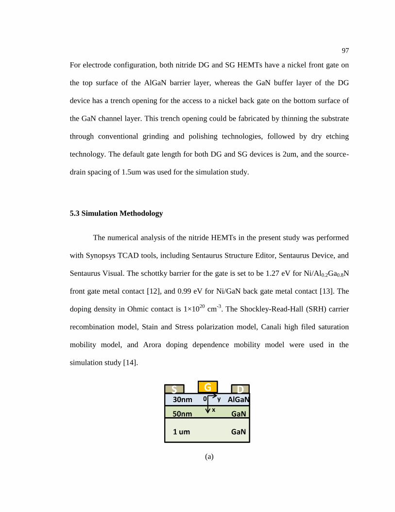
97
For electrode configuration, both nitride DG and SG HEMTs have a nickel front gate on
the top surface of the AlGaN barrier layer, whereas the GaN buffer layer of the DG
device has a trench opening for the access to a nickel back gate on the bottom surface of
the GaN channel layer. This trench opening could be fabricated by thinning the substrate
through conventional grinding and polishing technologies, followed by dry etching
technology. The default gate length for both DG and SG devices is 2um, and the source-
drain spacing of 1.5um was used for the simulation study.
5.3 Simulation Methodology
The numerical analysis of the nitride HEMTs in the present study was performed
with Synopsys TCAD tools, including Sentaurus Structure Editor, Sentaurus Device, and
Sentaurus Visual. The schottky barrier for the gate is set to be 1.27 eV for Ni/Al0.2Ga0.8N
front gate metal contact [12], and 0.99 eV for Ni/GaN back gate metal contact [13]. The
doping density in Ohmic contact is 1×10²⁰
cm-3
. The Shockley-Read-Hall (SRH) carrier
recombination model, Stain and Stress polarization model, Canali high filed saturation
mobility model, and Arora doping dependence mobility model were used in the
simulation study [14].
(a)
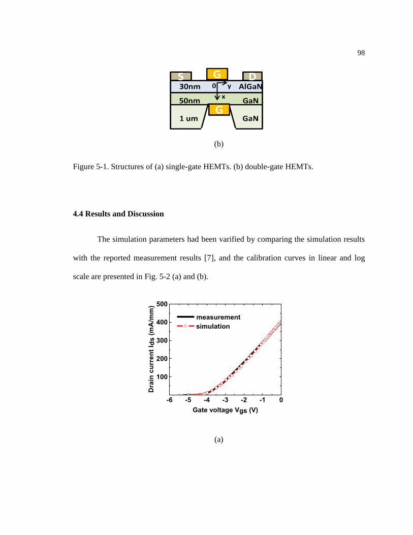
98
(b)
Figure 5-1. Structures of (a) single-gate HEMTs. (b) double-gate HEMTs.
4.4 Results and Discussion
The simulation parameters had been varified by comparing the simulation results
with the reported measurement results [7], and the calibration curves in linear and log
scale are presented in Fig. 5-2 (a) and (b).
-6 -5 -4 -3 -2 -1 0
100
200
300
400
500
Dra
in c
urr
en
t I d
s (
mA
/mm
)
Gate voltage Vgs (V)
measurement
simulation
(a)
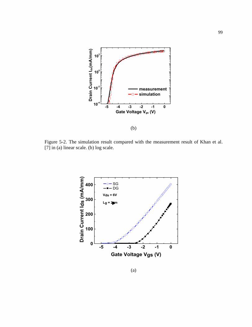
99
-5 -4 -3 -2 -1 010
-4
10-2
100
102
Dra
in C
urr
en
t I d
s(m
A/m
m)
Gate Voltage Vgs (V)
measurement
simulation
(b)
Figure 5-2. The simulation result compared with the measurement result of Khan et al.
[7] in (a) linear scale. (b) log scale.
-5 -4 -3 -2 -1 00
100
200
300
400
Vds = 6V
Lg = 2m
Dra
in C
urr
en
t I d
s (
mA
/mm
)
Gate Voltage Vgs (V)
SG
DG
(a)
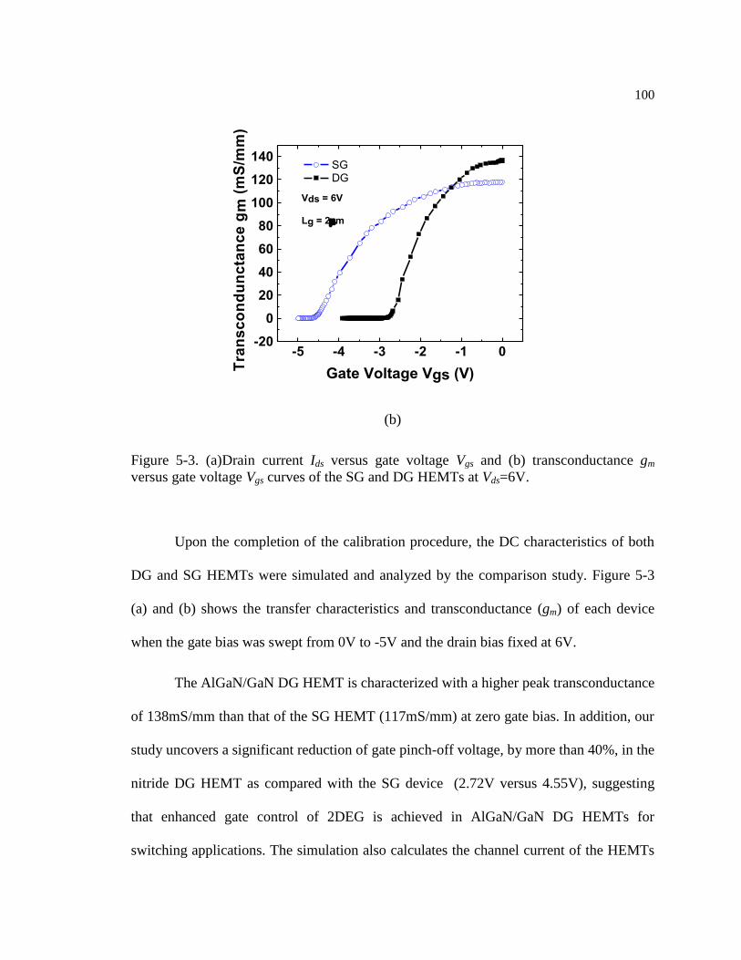
100
-5 -4 -3 -2 -1 0-20
0
20
40
60
80
100
120
140
Vds = 6V
Lg = 2m T
ran
sc
on
du
nc
tan
ce
gm
(m
S/m
m)
Gate Voltage Vgs (V)
SG
DG
(b)
Figure 5-3. (a)Drain current Ids versus gate voltage Vgs and (b) transconductance gm
versus gate voltage Vgs curves of the SG and DG HEMTs at Vds=6V.
Upon the completion of the calibration procedure, the DC characteristics of both
DG and SG HEMTs were simulated and analyzed by the comparison study. Figure 5-3
(a) and (b) shows the transfer characteristics and transconductance (gm) of each device
when the gate bias was swept from 0V to -5V and the drain bias fixed at 6V.
The AlGaN/GaN DG HEMT is characterized with a higher peak transconductance
of 138mS/mm than that of the SG HEMT (117mS/mm) at zero gate bias. In addition, our
study uncovers a significant reduction of gate pinch-off voltage, by more than 40%, in the
nitride DG HEMT as compared with the SG device (2.72V versus 4.55V), suggesting
that enhanced gate control of 2DEG is achieved in AlGaN/GaN DG HEMTs for
switching applications. The simulation also calculates the channel current of the HEMTs
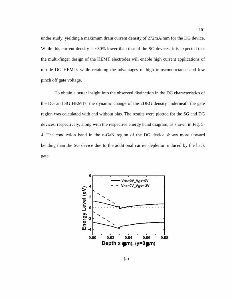
101
under study, yielding a maximum drain current density of 272mA/mm for the DG device.
While this current density is ~30% lower than that of the SG devices, it is expected that
the multi-finger design of the HEMT electrodes will enable high current applications of
nitride DG HEMTs while retaining the advantages of high transconductance and low
pinch off gate voltage.
To obtain a better insight into the observed distinction in the DC characteristics of
the DG and SG HEMTs, the dynamic change of the 2DEG density underneath the gate
region was calculated with and without bias. The results were plotted for the SG and DG
devices, respectively, along with the respective energy band diagram, as shown in Fig. 5-
4. The conduction band in the n-GaN region of the DG device shows more upward
bending than the SG device due to the additional carrier depletion induced by the back
gate.
0.00 0.02 0.04 0.06 0.08
-4
-2
0
2
4
6
En
erg
y L
ev
el
(eV
)
Depth x (m), (y=0m)
Vds=0V_Vgs=0V
Vds=0V_Vgs=-2V
(a)
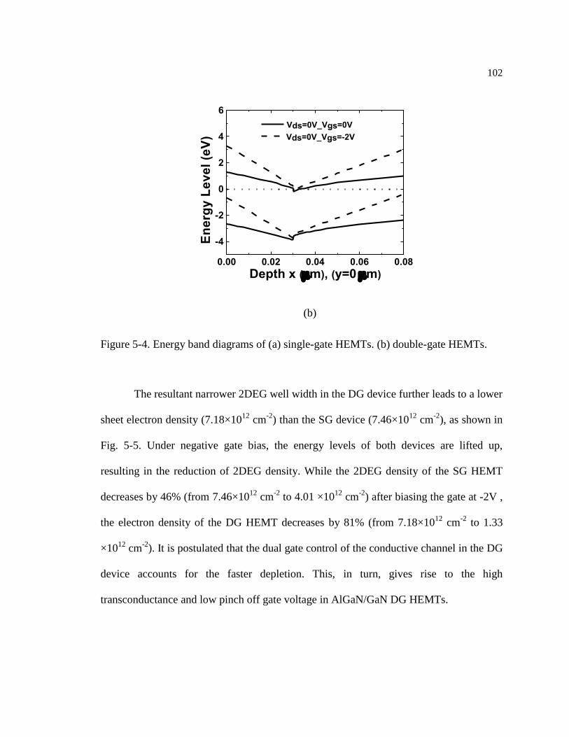
102
0.00 0.02 0.04 0.06 0.08
-4
-2
0
2
4
6
En
erg
y L
ev
el
(eV
)
Depth x (m), (y=0m)
Vds=0V_Vgs=0V
Vds=0V_Vgs=-2V
(b)
Figure 5-4. Energy band diagrams of (a) single-gate HEMTs. (b) double-gate HEMTs.
The resultant narrower 2DEG well width in the DG device further leads to a lower
sheet electron density (7.18×10¹²
cm-2
) than the SG device (7.46×10¹²
cm-2
), as shown in
Fig. 5-5. Under negative gate bias, the energy levels of both devices are lifted up,
resulting in the reduction of 2DEG density. While the 2DEG density of the SG HEMT
decreases by 46% (from 7.46×10¹²
cm-2
to 4.01 ×10¹²
cm-2
) after biasing the gate at -2V ,
the electron density of the DG HEMT decreases by 81% (from 7.18×10¹²
cm-2
to 1.33
×1012
cm-2
). It is postulated that the dual gate control of the conductive channel in the DG
device accounts for the faster depletion. This, in turn, gives rise to the high
transconductance and low pinch off gate voltage in AlGaN/GaN DG HEMTs.
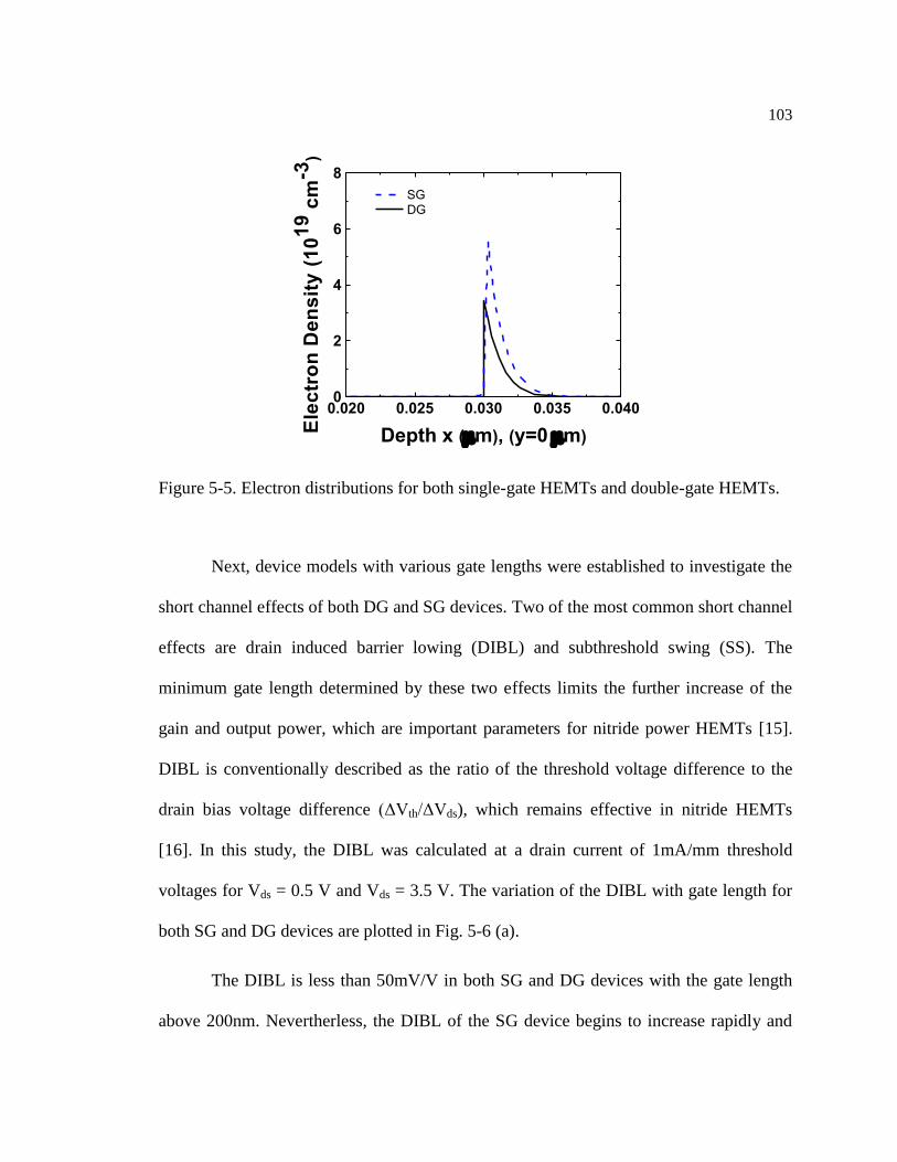
103
0.020 0.025 0.030 0.035 0.0400
2
4
6
8
E
lec
tro
n D
en
sit
y (
10
19
cm
-3)
Depth x (m), (y=0m)
SG
DG
Figure 5-5. Electron distributions for both single-gate HEMTs and double-gate HEMTs.
Next, device models with various gate lengths were established to investigate the
short channel effects of both DG and SG devices. Two of the most common short channel
effects are drain induced barrier lowing (DIBL) and subthreshold swing (SS). The
minimum gate length determined by these two effects limits the further increase of the
gain and output power, which are important parameters for nitride power HEMTs [15].
DIBL is conventionally described as the ratio of the threshold voltage difference to the
drain bias voltage difference (ΔVth/ΔVds), which remains effective in nitride HEMTs
[16]. In this study, the DIBL was calculated at a drain current of 1mA/mm threshold
voltages for Vds = 0.5 V and Vds = 3.5 V. The variation of the DIBL with gate length for
both SG and DG devices are plotted in Fig. 5-6 (a).
The DIBL is less than 50mV/V in both SG and DG devices with the gate length
above 200nm. Nevertherless, the DIBL of the SG device begins to increase rapidly and
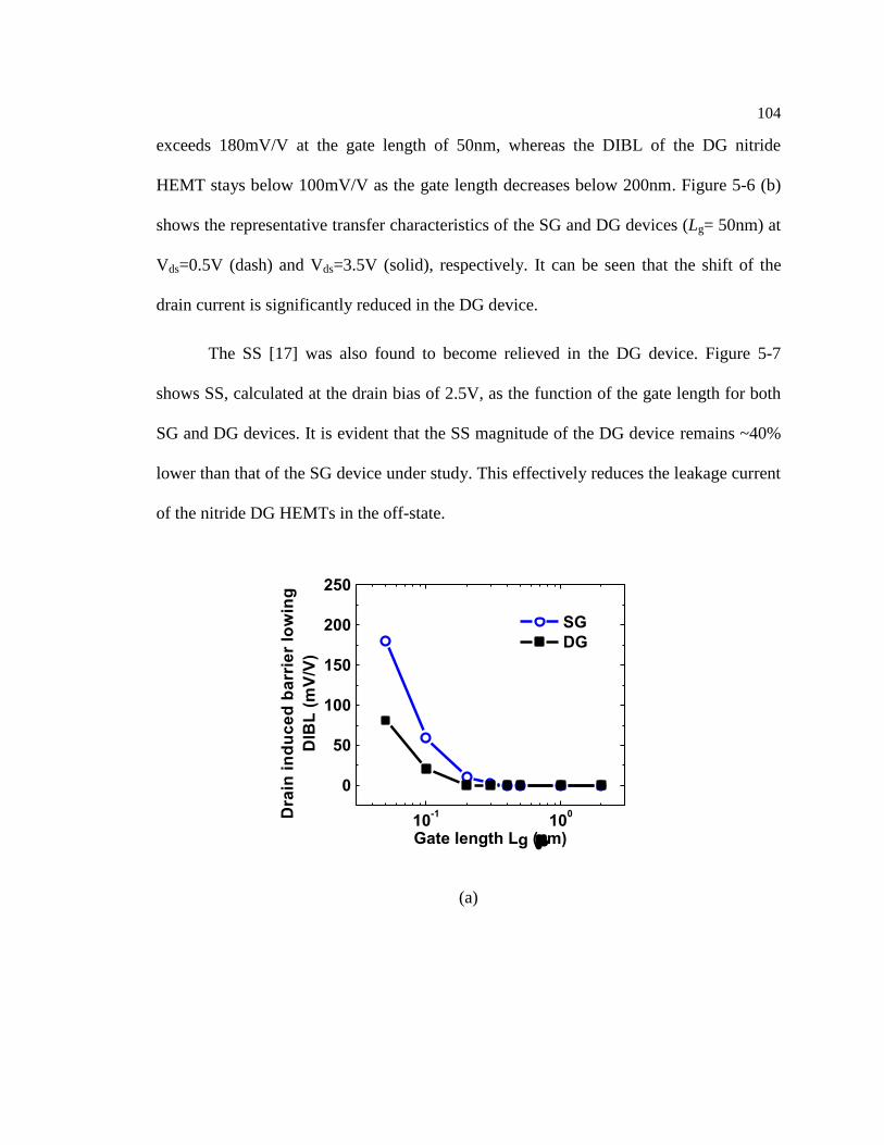
104
exceeds 180mV/V at the gate length of 50nm, whereas the DIBL of the DG nitride
HEMT stays below 100mV/V as the gate length decreases below 200nm. Figure 5-6 (b)
shows the representative transfer characteristics of the SG and DG devices (Lg= 50nm) at
Vds=0.5V (dash) and Vds=3.5V (solid), respectively. It can be seen that the shift of the
drain current is significantly reduced in the DG device.
The SS [17] was also found to become relieved in the DG device. Figure 5-7
shows SS, calculated at the drain bias of 2.5V, as the function of the gate length for both
SG and DG devices. It is evident that the SS magnitude of the DG device remains ~40%
lower than that of the SG device under study. This effectively reduces the leakage current
of the nitride DG HEMTs in the off-state.
10-1
100
0
50
100
150
200
250
Dra
in i
nd
uc
ed
ba
rrie
r lo
win
g
DIB
L (
mV
/V)
Gate length Lg (m)
SG
DG
(a)
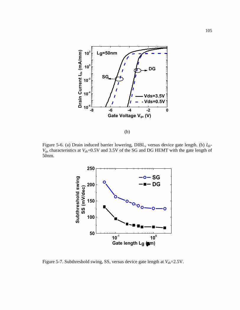
105
-8 -6 -4 -2 010
-6
10-4
10-2
100
102
DG
Dra
in C
urr
en
t I d
s (
mA
/mm
)
Gate Voltage Vgs (V)
Vds=3.5V
Vds=0.5V
SG
Lg=50nm
(b)
Figure 5-6. (a) Drain induced barrier lowering, DIBL, versus device gate length. (b) Ids-
Vgs characteristics at Vds=0.5V and 3.5V of the SG and DG HEMT with the gate length of
50nm.
10-1
100
50
100
150
200
250
Su
bth
res
ho
ld s
win
g
SS
(m
V/d
ec
)
Gate length Lg (m)
SG
DG
Figure 5-7. Subthreshold swing, SS, versus device gate length at Vds=2.5V.
106
The observed reduction of short channel effects in the DG device is consistent
with our aforementioned model analysis. Since the channel potential is controlled by both
gate bias and drain bias in a HEMT structure, the occurrence of DIBL and SS can be
attributed to the reinforced drain influence in the short channel devices and subsequently
the diminished gate control over the channel potential. The enhanced gate control
capability of nitride DG HEMTs, resulting from the effective depletion of channel
electrons via dual gate architecture, weakens the drain influence in the DG device, and
thus suppresses the short channel effects. The suppressed drain bias effect on the channel
potential can be observed directly from Fig. 5-8, which shows the channel potential of
each device under two different drain biases. The gate bias is set to be -5.2V for the SG
device and -3.5V for the DG device to pinch off both devices. It is evident that the
channel potential in the DG device does not increase as much as the one in the SG device.
The lower channel potential, in turn, offers the DG device more immunity to the short
channel effects than the SG device.
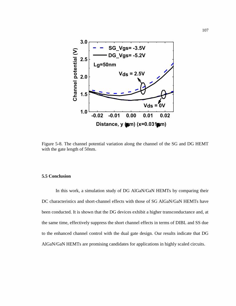
107
-0.02 -0.01 0.00 0.01 0.021.0
1.5
2.0
2.5
3.0
Vds = 0V
Ch
an
ne
l p
ote
nti
al
(V)
Distance, y (m) (x=0.031m)
SG_Vgs= -3.5V
DG_Vgs= -5.2V
Vds = 2.5V
Lg=50nm
Figure 5-8. The channel potential variation along the channel of the SG and DG HEMT
with the gate length of 50nm.
5.5 Conclusion
In this work, a simulation study of DG AlGaN/GaN HEMTs by comparing their
DC characteristics and short-channel effects with those of SG AlGaN/GaN HEMTs have
been conducted. It is shown that the DG devices exhibit a higher transconductance and, at
the same time, effectively suppress the short channel effects in terms of DIBL and SS due
to the enhanced channel control with the dual gate design. Our results indicate that DG
AlGaN/GaN HEMTs are promising candidates for applications in highly scaled circuits.
108
Reference
1. Keisuke Shinohara, Dean C. Regan, Yan Tang, Andrea L. Corrion, David F. Brown,
Joel C. Wong, John F. Robinson, Helen H. Fung, Adele Schmitz, Thomas C. Oh,
Samuel Jungjin Kim, Peter S. Chen, Robert G. Nagele, Alexandros D. Margomenos,
and Miroslav Micovic: Scaling of GaN HEMTs and Schottky Diodes for
Submillimeter-Wave MMIC Applications. IEEE Transactions on Electron Devices
60, 2982 (2013)
2. W. Chung, E. Hoke, E. M. Chumbes, and T. Palacios: AlGaN/GaN HEMT With 300-
GHz fmax. IEEE Electron Device Lett. 31, 195 (2010)
3. S. Bouzid-Driad, H. Maher, N. Defrance, V. Hoel, J. –C. De Jaeger, M. Renvoise,
and P. Frijlink: AlGaN/GaN HEMTs on Silicon Substrate With 206-GHz FMAX. IEEE
Electron Device Lett. 34, 36 (2013)
4. Gregg H. Jessen, Robert C. Fitch, James K. Gillespie, Glen Via, Antonio Crespo,
Derrick Langley, Daniel J. Denninghoff, Manuel Trejo, Eric R. Heller: Short-Channel
Effect Limitations on High-Frequency Operation of AlGaN/GaN HEMTs for T-Gate
Devices. IEEE Transactions on Electron Devices 54, 2589 (2007)
5. T. Palacios, A. Chakraborty, S. Heikman, S. Keller, S. DenBaars, and U. Mishra:
AlGaN/GaN high electron mobility transistors with InGaN back-barriers. IEEE
Electron Device Lett. 27, 13 (2006)
6. Ramakrishna Vetury, Naiqain Q. Zhang, Stacia Keller, and Umesh K. Mishra: The
Impact of Surface States on the DC and RF Characteristics of AlGaN/GaN HFETs.
IEEE TRANSACTIONS ON ELECTRON DEVICES 48, 3 (2001)
109
7. M. A. Khan, X. Hu, G. Simin, A. Lunev, J. Yang, R. Gaska, and M. S. Shur:
AlGaN/GaN metal oxide semiconductor heterostructure field effect transistor. IEEE
Electron Device Lett. 21, 63 (2001)
8. T. Sekigawa and Y. Hayashi: Calculated threshold-voltage characteristics of an
XMOS transistor having an additional bottom gate. Solid State Electron 27, 827
(1984)
9. Xinnan Lin, Chuguang Feng, Shengdong Zhang, Wai-Hung Ho, Mansun Chan:
Characterization of double gate MOSFETs fabricated by a simple method on a
recrystallized silicon film. Solid-sate electronics 48, 2315 (2004)
10. Beatriz G. Vasallo, Nicolas Wichmann, Sylvain Bollaert, Yannick Roelens, Alain
Cappy, Tomas Gonzalez, Daniel Pardo, Javier Mateos: Comparison Between the
Dynamic Performance of Double- and Single-Gate AlInAs/InGaAs HEMTs. IEEE
Transactions on Electron Devices 54, 2815 (2007)
11. N. Lakhdar, F. Djeffal, and Z. Dibi: A TwoDimensional Numerical Analysis of
Subthreshold Performances for DoubleGate GaNMESFETs. in AIP Conf. Proc.,
Strasbourg, France, 8–10 October 2010, 1292, 173 (2010)
12. D. Qiao, L. S. Yu, S. S. Lau, J. M. Redwing: Dependence of Ni/AlGaN Schottky
barrier height on Al mole fraction. Journal of Applied Physics 87, 801 (2000)
13. A C Schmitzy, A T Pingy, M Asif Khanz, Q Chenz, J W Yangz, and I Adesida:
Schottky barrier properties of various metals on n-type GaN. Semiconductor Science
Technology 11, 1464 (1996)
14. Sentaurus User’s Guide, Synopsys, Inc (2009)
110
15. S.M. Razavi, S.H.Zahiri, S.E.Hosseini: A novel AlGaN/GaN HEMT with a p-layer in
the barrier. Physica E 54, 24 (2013)
16. Pil Sung Park and Siddharth Rajan: Simulation of Short-Channel Effects in N- and
Ga-Polar AlGaN/GaN HEMTs. IEEE Transactions on Electron Devices 58, 704
(2011)
17. Simon M. Sze, Kwok K. Ng: Physics of Semiconductor Devices, 3rd Edition. John
Wiley & Sons (2006)
Chapter 6
Temperature dependence of AlInN/GaN HEMTs electrical characteristics
In this chapter, the electrical properties of AlInN/GaN HEMTs from room
temperature down to 50K have been investigated. The results show that the reduction of
the device operating temperature leads to the enhancement of the drain saturation current
and transconductance. Over the entire temperature range, a self-heating effect when the
power consumption is high has been observed. Moreover, the relationship between
electron density and channel electron mobility is studied in detail. It is concluded that in
the presence of high negative gate bias, electrons at the AlInN/GaN interface will be
pushed into the bulk GaN buffer layer, and these electrons combined with Coulomb
scattering causes the electron mobility reduction at high reverse gate voltage.
6.1 Introduction
AlInN/GaN high electron mobility transistors (HEMTs) have been a new favorite
for high-power radio frequency (RF) applications recently [1-5]. The sheet charge density
of two-dimensional electron gas (2DEG) induced is much higher in AlInN/GaN HEMTs
than AlGaN/GaN HEMTs [6]. Meanwhile, the lattice-mached AlInN/GaN heterostructure
leads to the elimination of stress and piezopolarization effect and have enormous
pontential in the improvement of heterostructure stability and the reduction or
disappearance of the current collapse related to the surface states [7-9]. Considerable
112
achievements have been obtained as the improvements of material quality and device
fabrication techniques [1, 3].
GaN-based HEMTs are expected to have advanced performance under cryogenic
operation temperatures due to the reduction of self-heating and scattering in 2DEG.
Cryogenic electrical characteristics of AlGaN/GaN HEMTs are investigated by several
research works, revealing that the more remarkable “current-kink” effect in lower
temperatures and the enhancement of cutoff frequency and transconductance under
cryogenic temperatures [10, 11]. However, to date most reports involve the investigation
of GaN-based HEMTs in the cryogenic temperature range are based on the studies of
AlGaN/GaN HEMTs, few reports about the performance of AlInN/GaN HEMTs is
carried out.
In this study, the detail cryogenic properties of AlInN/GaN HEMTs are
investigated by both DC and pulse measurements over the temperature range of 50K ~
295K. The C-V measurement results of gate capacitance and gate voltage combined with
the channel conductance values give the temperature dependent characteristics between
the channel electron mobility and the 2DEG density.
6.2 Aluminium Indium Nitride/Gallium Nitride heterostructure
The lattice constant of AlInN with indium composition around 17% is the same as
the one of GaN [32]. As shown in Fig. 5-1, the GaN layer and the Al0.83In0.17N layer are
lattice matched at 3.2. Since there is no mismatch between the two layers, piezoelectric
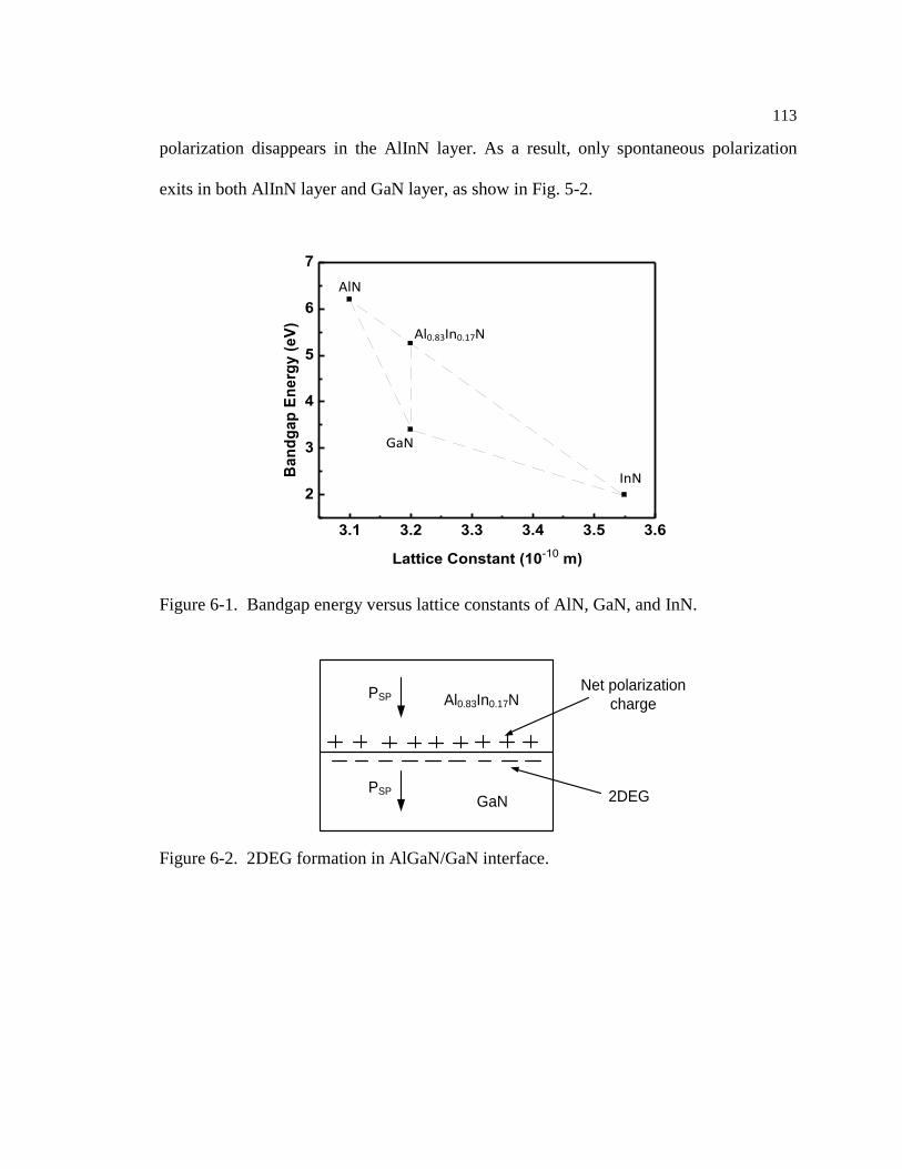
113
polarization disappears in the AlInN layer. As a result, only spontaneous polarization
exits in both AlInN layer and GaN layer, as show in Fig. 5-2.
3.1 3.2 3.3 3.4 3.5 3.6
2
3
4
5
6
7
Ba
nd
ga
p E
ne
rgy
(e
V)
Lattice Constant (10-10 m)
AlN
InN
GaN
Al0.83In0.17N
Figure 6-1. Bandgap energy versus lattice constants of AlN, GaN, and InN.
PSP
PSP
Al0.83In0.17N
GaN
Net polarization
charge
2DEG
Figure 6-2. 2DEG formation in AlGaN/GaN interface.
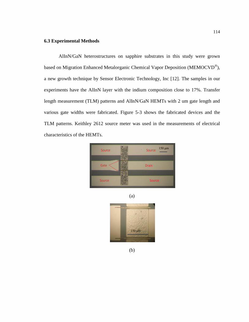
114
6.3 Experimental Methods
AlInN/GaN heterostructures on sapphire substrates in this study were grown
based on Migration Enhanced Metalorganic Chemical Vapor Deposition (MEMOCVD®),
a new growth technique by Sensor Electronic Technology, Inc [12]. The samples in our
experiments have the AlInN layer with the indium composition close to 17%. Transfer
length measurement (TLM) patterns and AlInN/GaN HEMTs with 2 um gate length and
various gate widths were fabricated. Figure 5-3 shows the fabricated devices and the
TLM patterns. Keithley 2612 source meter was used in the measurements of electrical
characteristics of the HEMTs.
(a)
(b)
150 μm
150 μm
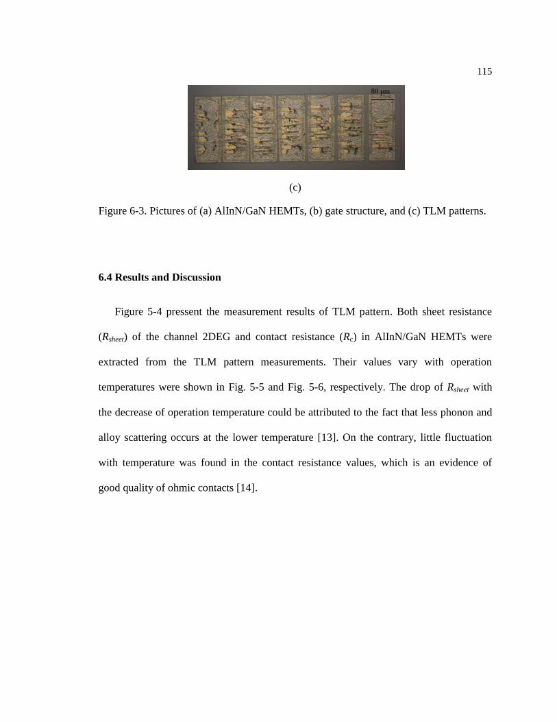
115
(c)
Figure 6-3. Pictures of (a) AlInN/GaN HEMTs, (b) gate structure, and (c) TLM patterns.
6.4 Results and Discussion
Figure 5-4 pressent the measurement results of TLM pattern. Both sheet resistance
(Rsheet) of the channel 2DEG and contact resistance (Rc) in AlInN/GaN HEMTs were
extracted from the TLM pattern measurements. Their values vary with operation
temperatures were shown in Fig. 5-5 and Fig. 5-6, respectively. The drop of Rsheet with
the decrease of operation temperature could be attributed to the fact that less phonon and
alloy scattering occurs at the lower temperature [13]. On the contrary, little fluctuation
with temperature was found in the contact resistance values, which is an evidence of
good quality of ohmic contacts [14].
80 μm
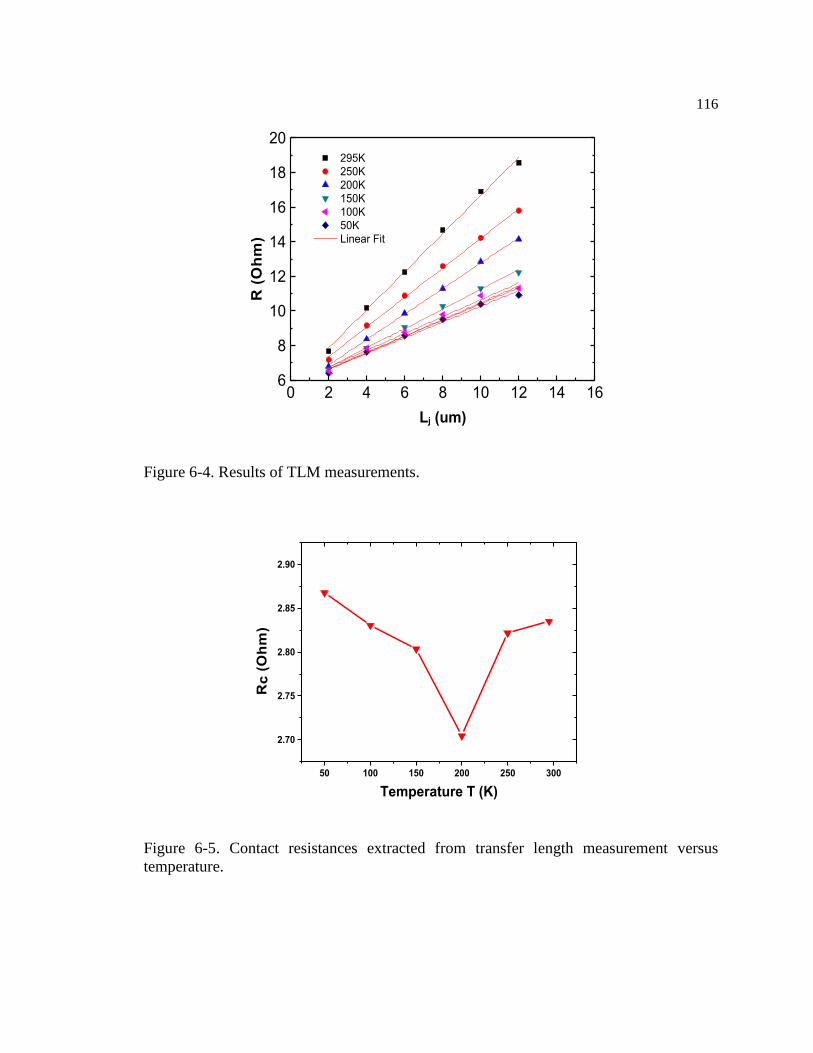
116
0 2 4 6 8 10 12 14 166
8
10
12
14
16
18
20
295K
250K
200K
150K
100K
50K
Linear Fit
R (
Oh
m)
Lj (um)
Figure 6-4. Results of TLM measurements.
50 100 150 200 250 300
2.70
2.75
2.80
2.85
2.90
Rc
(O
hm
)
Temperature T (K)
Figure 6-5. Contact resistances extracted from transfer length measurement versus
temperature.
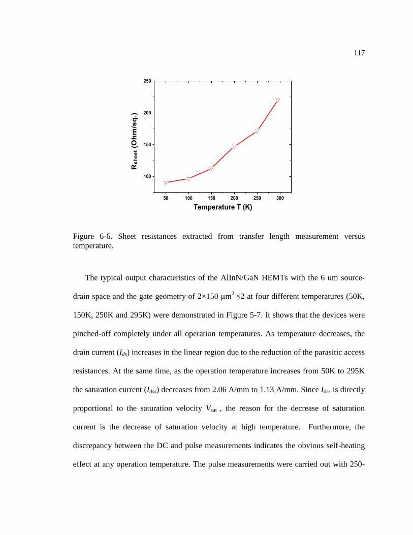
117
50 100 150 200 250 300
100
150
200
250
Rs
he
et (O
hm
/sq
.)
Temperature T (K)
Figure 6-6. Sheet resistances extracted from transfer length measurement versus
temperature.
The typical output characteristics of the AlInN/GaN HEMTs with the 6 um source-
drain space and the gate geometry of 2×150 μm2
×2 at four different temperatures (50K,
150K, 250K and 295K) were demonstrated in Figure 5-7. It shows that the devices were
pinched-off completely under all operation temperatures. As temperature decreases, the
drain current (Ids) increases in the linear region due to the reduction of the parasitic access
resistances. At the same time, as the operation temperature increases from 50K to 295K
the saturation current (Idss) decreases from 2.06 A/mm to 1.13 A/mm. Since Idss is directly
proportional to the saturation velocity Vsat , the reason for the decrease of saturation
current is the decrease of saturation velocity at high temperature. Furthermore, the
discrepancy between the DC and pulse measurements indicates the obvious self-heating
effect at any operation temperature. The pulse measurements were carried out with 250-
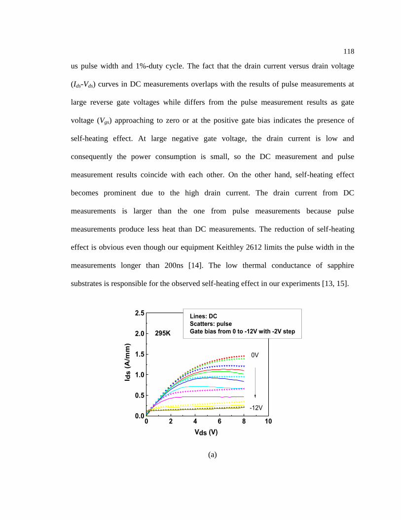
118
us pulse width and 1%-duty cycle. The fact that the drain current versus drain voltage
(Ids-Vds) curves in DC measurements overlaps with the results of pulse measurements at
large reverse gate voltages while differs from the pulse measurement results as gate
voltage (Vgs) approaching to zero or at the positive gate bias indicates the presence of
self-heating effect. At large negative gate voltage, the drain current is low and
consequently the power consumption is small, so the DC measurement and pulse
measurement results coincide with each other. On the other hand, self-heating effect
becomes prominent due to the high drain current. The drain current from DC
measurements is larger than the one from pulse measurements because pulse
measurements produce less heat than DC measurements. The reduction of self-heating
effect is obvious even though our equipment Keithley 2612 limits the pulse width in the
measurements longer than 200ns [14]. The low thermal conductance of sapphire
substrates is responsible for the observed self-heating effect in our experiments [13, 15].
0 2 4 6 8 100.0
0.5
1.0
1.5
2.0
2.5
-12V
Lines: DC
Scatters: pulse
Gate bias from 0 to -12V with -2V step
I ds
(A
/mm
)
Vds (V)
295K
0V
(a)
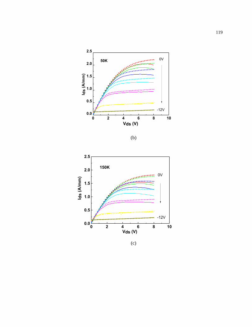
119
0 2 4 6 8 100.0
0.5
1.0
1.5
2.0
2.5
Vds (V)
I ds
(A
/mm
)
50K
-12V
0V
(b)
0 2 4 6 8 100.0
0.5
1.0
1.5
2.0
2.5
I ds
(A
/mm
)
Vds (V)
150K
-12V
0V
(c)
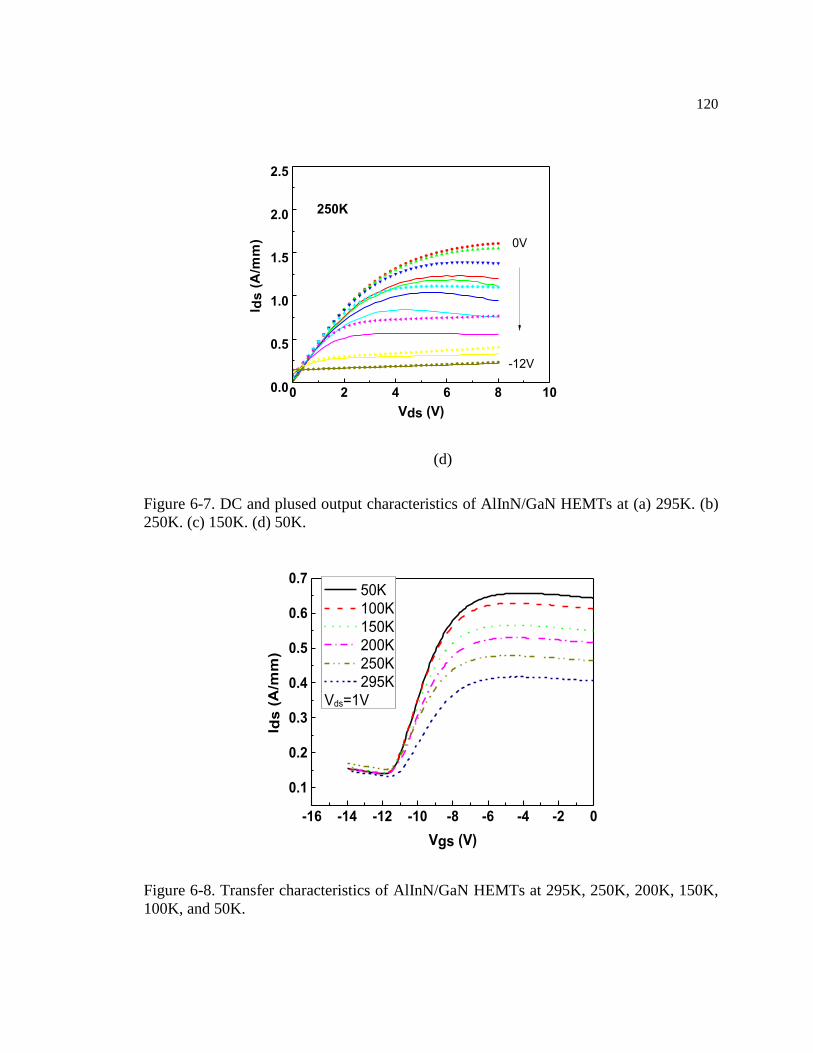
120
0 2 4 6 8 100.0
0.5
1.0
1.5
2.0
2.5
I ds
(A
/mm
)
Vds (V)
250K
-12V
0V
(d)
Figure 6-7. DC and plused output characteristics of AlInN/GaN HEMTs at (a) 295K. (b)
250K. (c) 150K. (d) 50K.
-16 -14 -12 -10 -8 -6 -4 -2 0
0.1
0.2
0.3
0.4
0.5
0.6
0.7
I ds
(A
/mm
)
Vgs (V)
50K
100K
150K
200K
250K
295K
Vds=1V
Figure 6-8. Transfer characteristics of AlInN/GaN HEMTs at 295K, 250K, 200K, 150K,
100K, and 50K.
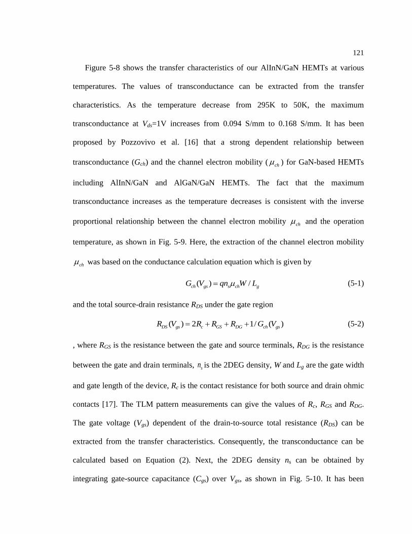
121
Figure 5-8 shows the transfer characteristics of our AlInN/GaN HEMTs at various
temperatures. The values of transconductance can be extracted from the transfer
characteristics. As the temperature decrease from 295K to 50K, the maximum
transconductance at Vds=1V increases from 0.094 S/mm to 0.168 S/mm. It has been
proposed by Pozzovivo et al. [16] that a strong dependent relationship between
transconductance (Gch) and the channel electron mobility ( ch ) for GaN-based HEMTs
including AlInN/GaN and AlGaN/GaN HEMTs. The fact that the maximum
transconductance increases as the temperature decreases is consistent with the inverse
proportional relationship between the channel electron mobility ch and the operation
temperature, as shown in Fig. 5-9. Here, the extraction of the channel electron mobility
ch was based on the conductance calculation equation which is given by
( ) /ch gs s ch gG V qn W L (5-1)
and the total source-drain resistance RDS under the gate region
( ) 2 1/ ( )DS gs c GS DG ch gsR V R R R G V (5-2)
, where RGS is the resistance between the gate and source terminals, RDG is the resistance
between the gate and drain terminals, sn is the 2DEG density, W and Lg are the gate width
and gate length of the device, Rc is the contact resistance for both source and drain ohmic
contacts [17]. The TLM pattern measurements can give the values of Rc, RGS and RDG.
The gate voltage (Vgs) dependent of the drain-to-source total resistance (RDS) can be
extracted from the transfer characteristics. Consequently, the transconductance can be
calculated based on Equation (2). Next, the 2DEG density ns can be obtained by
integrating gate-source capacitance (Cgs) over Vgs, as shown in Fig. 5-10. It has been
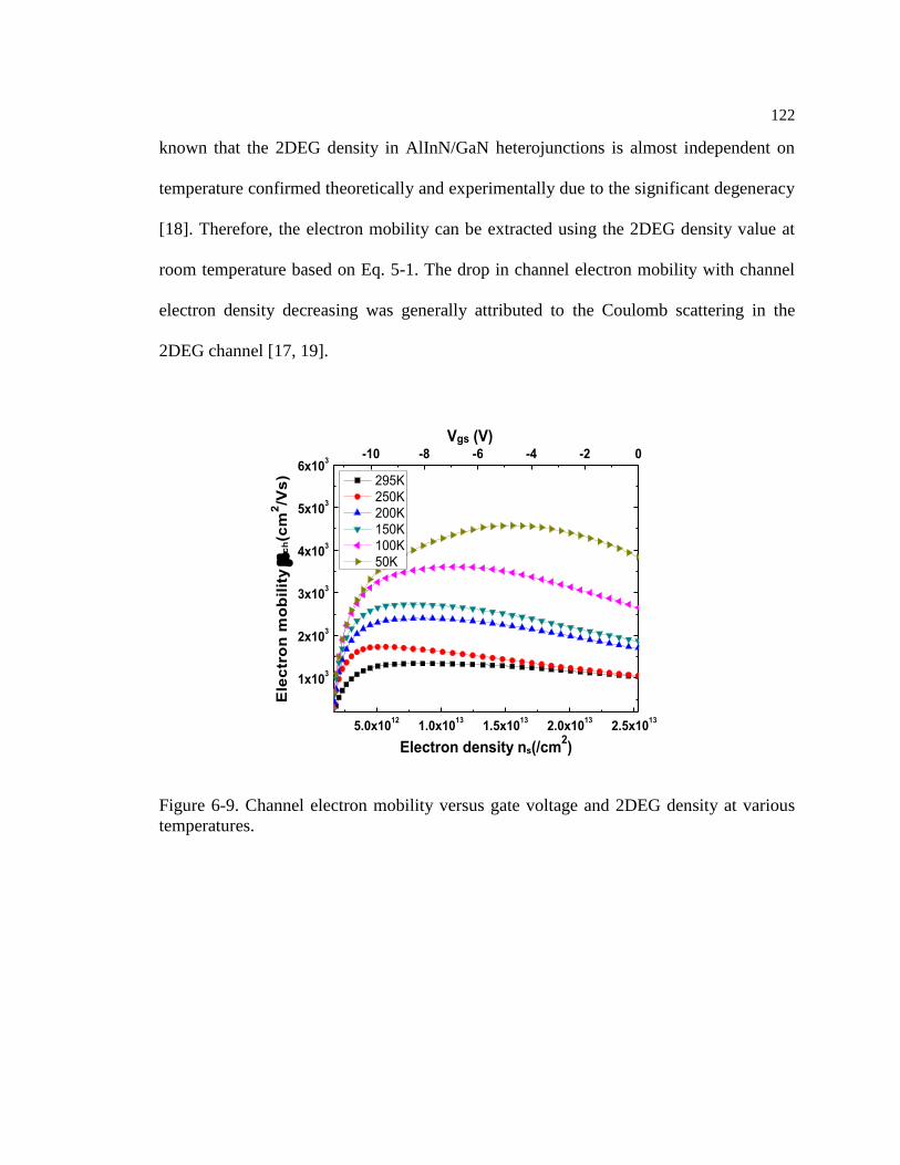
122
known that the 2DEG density in AlInN/GaN heterojunctions is almost independent on
temperature confirmed theoretically and experimentally due to the significant degeneracy
[18]. Therefore, the electron mobility can be extracted using the 2DEG density value at
room temperature based on Eq. 5-1. The drop in channel electron mobility with channel
electron density decreasing was generally attributed to the Coulomb scattering in the
2DEG channel [17, 19].
5.0x10¹²
1.0x10¹³
1.5x10¹³
2.0x10¹³
2.5x10¹³
1x10³
2x10³
3x10³
4x10³
5x10³
6x10³
Ele
ctr
on
mo
bil
ity
c
h(c
m2/V
s)
Electron density ns(/cm2)
295K
250K
200K
150K
100K
50K
-10 -8 -6 -4 -2 0
Vgs (V)
Figure 6-9. Channel electron mobility versus gate voltage and 2DEG density at various
temperatures.
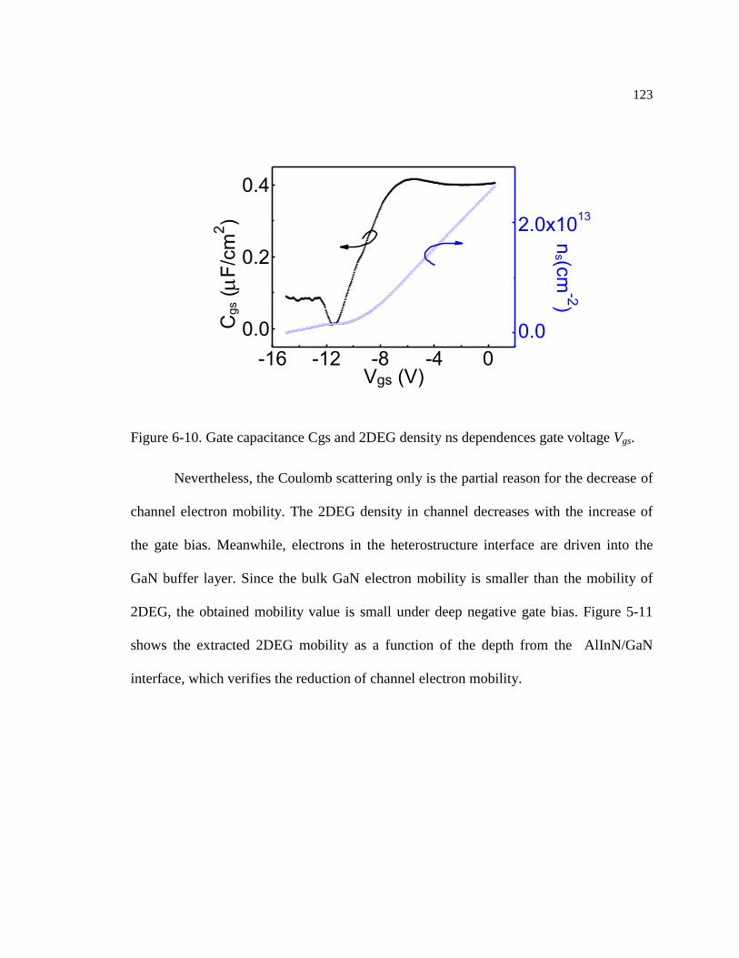
123
-16 -12 -8 -4 0
0.0
0.2
0.4
Vgs (V)
Cgs (
F/c
m2)
0.0
2.0x10¹³
ns (c
m-2)
Figure 6-10. Gate capacitance Cgs and 2DEG density ns dependences gate voltage Vgs.
Nevertheless, the Coulomb scattering only is the partial reason for the decrease of
channel electron mobility. The 2DEG density in channel decreases with the increase of
the gate bias. Meanwhile, electrons in the heterostructure interface are driven into the
GaN buffer layer. Since the bulk GaN electron mobility is smaller than the mobility of
2DEG, the obtained mobility value is small under deep negative gate bias. Figure 5-11
shows the extracted 2DEG mobility as a function of the depth from the AlInN/GaN
interface, which verifies the reduction of channel electron mobility.
124
20 40 60 80 100 120 140 160 180 200100
1000
10000
Ele
ctr
on
mo
bil
ity
(c
m2/V
s)
Depth in channel (nm)
295K
250K
200K
150K
100K
50K
Figure 6-11. Extracted 2DEG mobility as a function of the depth from the AlInN/GaN
interface
The value of channel mobility ch quickly reduces to the value of electron
mobility in bulk GaN, which is 100-400 cm2/Vs at room temperature [12], when
electrons are driven into the GaN buffer layer. Moreover, it also can be observed that the
channel mobility ch decrease from its maximum value at each temperature. Alloy
scattering, phonon scattering, and interface roughness are not all the factors responsible
for this reduction because the decrease also occurs at temperature as low as 50K under
which alloy scattering and phonon scattering could be neglected [20]. Also, other
proposed mechanism that electrons from the channel diffuse into the AlInN layer forming
a parasitic parallel conduction channel with low electron mobility cannot explain the
decrease of electron mobility at high 2DEG density in our case [19]. From Fig. 5-9, it can
be seen that electron mobility begins to reduce at a low gate bias. The parasitic parallel
125
conduction channel should not be activated at such bias condition. This is also confirmed
by the fact that the measured value of gate capacitance keeps constant while the electron
mobility decreases, as shown in Fig. 5-10. Thus, intersub-band scattering in the
AlInN/GaN heterostructure potential well should be the reason for the electron mobility
drop under low reverse gate bias [21].
5.5 Conclusion
In summary, the DC and pulse electrical properties of AlInN/GaN HEMTs were
investigated in low temperature. The experimental results show that the DC saturation
current improves from 1.13 A/mm to 2.06 A/mm. Meanwhile, the maximum
transconductance at Vds=1V increases from 0.094 S/mm to 0.168 S/mm when the
operation temperature was cooled down from room temperature to 50K. The electron
mobility decreases at the low 2DEG density region because of strong Coulomb scattering
and at the high 2DEG density region because of strong intersubband scattering. Because
of low thermal conductance of sapphire substrates, self-heating effect can be detected at
all operation temperature. Therefore, it is necessary to use substrates with high thermal
conductivity to further reduce the self-heating effect. Furthermore, it is concluded that the
drop in electron mobility under high negative gate voltage is partially due to the electrons
are drifted to the GaN buffer layer by the high electric field.
126
Reference
1. Sarazin N, Morvan E, di Forte Poisson M A, Oualli M, Gaqui`ere C, Jardel O, Drisse
O, Tordjman M, Magis M and Delage S L, AlInN/AlN/GaN HEMT Technology on
SiC With 10-W/mm and 50% PAE at 10 GHz, 2010 IEEE Electron Dev. Lett. 31 11.
2. Duan B X and Yang Y T, Breakdown voltage analysis of Al0.25Ga0.75N/GaN high
electron mobility transistors with partial silicon doping in the AlGaN layer 2012
Chin. Phys. B 21 057201.
3. Tirelli S, Marti D, Sun H F, Alt A R, Carlin J F C, Grandjean N and Bolognesi C R,
Fully Passivated AlInN/GaN HEMTs With fT/fMAX of 205/220 GHz, 2011 IEEE
Electron Dev. Lett. 32 1364.
4. Chabak K D, Trejo M, Crespo A,Walker D E, Yang J, Gaska R, Kossler M, Gillespie
J K, Jessen G H, Trimble V and Via G D, Strained AlInN/GaN HEMTs on SiC With
2.1-A/mm Output Current and 104-GHz Cutoff Frequency, 2010 IEEE Electron Dev.
Lett. 31 561.
5. Mao W, Yang C, Hao Y, Zhang J C, Liu H X , Bi Z W, Xu S R, Xue J S, Ma X H,
Wang C, Yang L A, Zhang J F and Kuang X W, Development and characteristic
analysis of a field-plated Al2O3/AlInN/GaN MOS-HEMT, 2011 Chin. Phys. B 20
017203.
6. Sattu A, Billingsley D, Deng J, Yang J, Gaska R, Shur M and Simin G 2011 The 69th
Device Research Conference June 20–22, 2011 University of California, Santa
Barbara, CA, USA, p. 55.
127
7. Vetury R, Zhang Q, Keller S and Mishra U K, The impact of surface states on the DC
and RF characteristics of AlGaN/GaN HFETs, 2001 IEEE Trans. Electron Dev. 48
560
8. Leach J H, Wu M, Ni X, Li X, Ozgur U and Morkoc H, Effect of lattice mismatch on
gate lag in high quality InAlN/AlN/GaN HFET structures, 2010 Phys. Status Solidi A
207 211
9. Mikulics M, Stoklas R, Dadgar A, Greguˇsov´a D, Nov´ak J, Gr¨utzmacher D, Krost
A and Kordoˇs P, InAlN/GaN/Si heterostructures and field-effect transistors with
lattice matched and tensely or compressively strained InAlN, 2010 Appl. Phys. Lett.
97 173505
10. Lin C H, Wang W K, Lin P C, Lin C K, Chang Y J and Chan Y J, Transient pulsed
analysis on GaN HEMTs at cryogenic temperatures, 2005 IEEE Electron Dev. Lett.
26 710
11. Endoh A, Watanabe I, Yamashita1 Y, Mimura T and Matsui T, Effect of temperature
on cryogenic characteristics of AlGaN/GaN MIS-HEMTs, 2009 Phys. Status Solidi C
6 S964
12. Jinwey Y, Xuhong H, Deng J Y, Gaska R, Shur M and Simin G 2009 Proceedings of
the International Semiconductor Device Research Symposium December 9–11, 2009
College Park, Maryland, USA, p. 1
13. Morkoc H 2008 Handbook of Nitride Semiconductors and Devices (vol. 2)
(Weinheim: Wiley-VCH)
128
14. Qiao D, Yu L S, Jia L, Asbeck P M, Lau S S and Haynes T E, Transport properties of
the advancing interface ohmic contact to AlGaN/GaN heterostructures, 2002 Appl.
Phys. Lett. 80 992
15. Gaska R, Osinsky A, Yang JWand ShurMS, Self-heating in high-power AlGaN-GaN
HFETs, 1998 IEEE Electron Dev. Lett. 19 89
16. Pozzovivo G, Kuzmik J, Golka S, Schrenk W, Strasser G, Pogany D, Cico K, Tapajna
M, Frohich K, Carlin J F, Gonschorek M, Feltin E and Grandjean N, Gate insulation
and drain current saturation mechanism in InAlN/GaN metal-oxide-semiconductor
high-electron-mobility transistors, 2007 Appl. Phys. Lett. 91 043509
17. Levinshtein M E, Ivanov P A, Asif Khan M, Simin G, Zhang J, Hu X and Yang J,
Mobility enhancement in AlGaN/GaN metal-oxide-semiconductor heterostructure
field effect transistors, 2003 Semicond. Sci. Technol. 18 666
18. Tulek R, Iygaz A, Gokden S, Teke A, Ozturk M K and Kasap M, Effect of grain
boundary on local surface conductivity of diamond film, 2009 J. Appl. Phys. 105
13706
19. Dang X Z, Asbeck P M, Yu E T, Sullivan G J, Chen M Y, McDermott B T, Boutros
K S and Redwing J M, Measurement of drift mobility in AlGaN/GaN heterostructure
field-effect transistor, 1999 Appl. Phys. Lett. 74 3890
20. Ridley B K, Foutz B E and Eastman L F, Mobility of electrons in bulk GaN and
AlxGa1-xN/GaN heterostructures, 2000 Phys. Rev. B 61 16862
21. Marso M, Bernat J, Javorka P and Kordos P, Influence of a carrier supply layer on
carrier density and drift mobility of AlGaN/GaN/SiC high-electron-mobility
transistors, 2004 Appl. Phys. Lett. 84 2928.
129
Chapter 7
Energy transfer in quantum dots coupled microcavity nitride LEDs
In this chapter, quantum dots (QDs) coupled non-resonant microcavity light
emitting diodes (LEDs) are designed and an enhanced non-radiative energy transfer
between colloidal QD phosphors and InGaN/GaN quantum wells (QWs) is demonstrated.
It is the first time to improve the non-radiative energy transfer efficiency through
tailoring the radiative recombination lifetime of electron-hole pairs in QWs. The
microcavity structure is formed by a top metal reflector and a bottom distributed Bragg
reflector (DBR). The blue emission from the InGaN/GaN QWs is detuned from the
resonant modes of the microcavity to extend the radiative recombination lifetime in QWs.
The direct contact of QDs and the QW active layer is achieved by fabricating micro-holes
on the LEDs. The occurrence of non-radiative energy transfer between QW and QD is
confirmed by time-resolved photoluminescence (PL) measurement. A longer radiative
combination lifetime electron-hole pairs in the microcavity LEDs have been obtained in
the wavelength range from 440nm to 460nm in compared with the LEDs without
microcavity structure. The non-resonant microcavity structure, combining with the
micro-holes, leads to a 3.2 times enhancement of the effective quantum efficiency in
compare with the LEDs without microcavity structure.
7.1 Introduction
During last several decades, solid state lighting is replacing incandescent lamps
and fluorescent lamps in electrical lighting, and has been used in residential general
130
lighting, devices indicators, computer displays, and so on [1]. The advantages of solid
state lighting over the conventional lamps include higher convertible efficiency between
electrical energy and lighting, one hundred times longer lifetime than incandescent bulbs
and ten times longer lifetime than fluorescent lamps, and the high power intensity [2-4].
One of the core techniques involving in the solid state lighting is the white LED
technology. Currently, two main methods, multiple LEDs and phosphor based LEDs, are
employed in producing white emission in LEDs. Multiple LEDs method refers to
combine the LEDs which can emit the primary colors separately into a single lamp to
produce white emission. White emission will be formed when those three prime colors
are mixed. This method is a direct way but the cost is high due to the complication of
manufacture and the lamp size is large [5]. Another method is using phosphors to convert
a single color into multiple colors to obtain white lighting. Generally, nitride LEDs are
used as the blue light emitter and yellow phosphors is combined to convert the blue light
into the yellow light. A white light is yielded by mixing the blue light with the yellow
light. This method encounters the disadvantages of less than 100% phosphor convertible
efficiency and a poor color rendering property [29].
Recent years, colloidal compound QDs technique is becoming a new favorite
phosphor in the field of white LEDs. The lighting color emitted by this new phosphor
could be tuned in a large spectrum range. Comparing to other conventional phosphors,
the emission wavelength of quantum dots is sharper and the quantum efficiency is higher
[6, 7]. Without changing the chemical composition, QDs only need to adjust their sizes to
luminous a variety of colors. Besides the size-tunable emission wavelength, the
disclosure of a brand new way for electron-hole pairs between a bulk semiconductor and
131
QDs is another advantage that motivates the application of QDs in the white-LED
technique. Given QDs locating near the immediate vicinity of an InGaN QW, the free
carriers inside the QW could transfer the energy to the QDs in a special non-contact, non-
radiative way. This energy transfer method based on the dipole-dipole interactions
combining with the quantum well to QDs coupling effect [8]. This method skips several
color conversion steps, and thus is expected to have a higher luminous efficiency by
reduce the energy loss. Based on this method, core/shell CdSe/(Zn, Cd)S QDs have been
employed in white LED technique as phosphors combining with InGaN MQW LEDs [9-
11].
The configuration of the nitride LEDs plays an important role in improving the
non-radiative energy transfer rate between QWs and QDs. Since the non-radiative energy
transfer rate is in reversely proportional to the distance between QWs and QDs and the
non-radiative energy efficiency increases with the increase of the radiative recombination
lifetime of excitations in the QWs and with the increase of the nonradiative energy
transfer rate, prolonging the QW radiative combination lifetime and minimizing the QW-
QD distance are two approaches to enhance the non-radiative energy transfer efficiency.
Several studies have been carried out to increase the nonradiative energy transfer between
QW and QD. By using a very thin n-type capping layer (~5nm), a 13% measured color
conversion efficiency is achieved by Achermann et al. from an InGaN/GaN quantum well
to a single layer of CdSe/ZnS QDs [11]. However, the capping layer in this configuration
is too thin to be a good current spreading layer, leading to the decrease of the efficiency
of the LED itself. Moreover, the emission from the QD phosphor is still low compared to
the blue emission from the quantum well, resulting in an imbalanced white light emission
132
[10]. Chanyawadee et al.[12] proposed surface-patterned nitride LEDs with elliptical
holes reaching to the emissive quantum well layers. An average color conversion
efficiency of 20% was obtained by injecting QDs into the holes to make the short
distance between the QWs and the QDs [12]. In another work, Fan. et al. deposited
CdSe/ZnS QDs into the spaces in the nanopillar GaN LEDs to enhance the nonradiative
energy coupling between the quantum well and the QDs. A 263% increase in internal
quantum efficiency from that of planar GaN LEDs [10].
In this work a novel approach for improving non-radiative energy transfer
efficiency between QWs and QDs by depositing QDs into GaN-based LEDs with a non-
resonant microcavity structure is demonstrated. The non-resonant microcavity, consisting
of a narrow-band dielectric distributed Bragg reflector (DBR) lower layer and a
broadband metal reflector upper layer, is detuned from the blue emission from the
InGaN/GaN QWs to remarkably prolong the radiative recombination lifetime of electron-
hole pairs in the QWs which leads to the enhancement of the QW-QD non-radiative
energy transfer rate. The microcavity InGaN/GaN LEDs is patterned and dry-etched to
fabricate micro-holes that penetrate through the InGaN/GaN QWs. Colloidal QDs have
been deposited into these micro-holes to minimize the distance between QWs and QDs
for boosting the non-radiative energy transfer. The measured radiative combination
lifetime of QWs increases to 1.44 ns in microcavity LEDs from 1.24 ns in LEDs without
microcavity structure at the wavelength of 450 nm. Electroluminescence results show that
the effective quantum efficiency of the QDs coupled in microcavity LEDs is 3.2 times
than the one in control LEDs. At last, time-resolved photoluminescence study confirms
133
the occurrence of non-radiative energy transfer and an energy transfer rate which is
comparable to the radiative recombination rate is obtained.
7.2 Theory
7.2.1 Quantum dots and quantum confinement effect
QDs, also called “nanocrystals”, are crystals with very small dimensions which
are in the nanometer scale. The size of a QD is in the range of one to ten nanometers [13].
QDs are made from semiconductors, typically II-VI and III-V semiconductors [19]. They
are classified by their fabrication techniques. Colloidal QDs refers to a class of QDs that
are synthesized by wet chemical methods, which was first proposed by Murray et al. in
1993 [18]. In this method, QDs are grown from a solution containing the atomic species
that could build the nanocrystal blocks [17]. QDs used in this dissertation are CdSe/ZnS
QDs, which are core/cell semiconductor QDs. The bandgap energy of the shell material
(3.61 for ZnS) is much larger than the one of the core material (1.74 for CdSe). Thus, the
generated excitons are well restricted in the core. The shell material also can provide
good passivation for the surface defects of the core material to increase the fluorescence
quantum yield [19, 20].
Although QDs are semiconductors, they have certain unique optical and
electronic properties which cannot be obtained from bulk semiconductors. The
particularities of QDs derive from the existing quantum confinement effect in the QDs.
134
This quantum confinement effect endows QDs the tunable band gap energy which
influences the properties of QDs.
Quantum confinement effect is a concept of quantum mechanics, which varies the
band gap energy of QDs. According to the particle-wave duality which is a basic concept
of quantum mechanics, every particle associates a matter wave [14]. The rules of
quantum mechanics should be applied to the particles with the dimensions comparable to
the wavelength. In a bulk semiconductor material, carriers can move around the crystal
freely, which motion can be explained by integrating plane waves. However, in a
semiconductor material with the size comparable to its associated wavelength, the motion
of carriers could be described as a “particle in a box” [15]. Figure 6-1 (a) shows a simple
model for a particle in a one-dimensional potential box. The particle bounces back and
forth between two impenetrable walls with a constant speed [28]. The behavior of this
free particle can be described by the solutions of its Schrodinger equation with mass m
[16],
0)(2)(
22
2
xmE
dx
xd
(6-1)
Considering the boundary condition
0)()0( axx (6-2)
, the time-independent wave solution can be obtained as [16]
)sin(2
)(a
xn
ax
(6-3)
, where n is a positive integer number. Figure 6-1 (b) gives the first three solutions.
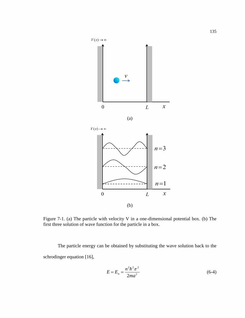
135
(a)
(b)
Figure 7-1. (a) The particle with velocity V in a one-dimensional potential box. (b) The
first three solution of wave function for the particle in a box.
The particle energy can be obtained by substituting the wave solution back to the
schrodinger equation [16],
2
222
2ma
nEE n
(6-4)
136
It can be seen that the energy levels of the particle are discrete and Wide wells
could lead to small energy level spaces.
Different from the bandgap energy of a bulk semiconductor Eg(bulk), the
bandgap energy of a QD Eg(qd) is size dependence. Given a sphere QD, the energy gap of
the QD can be calculated by [17]
d
e
mmd
hEE
she
gwell2
8.1)11
(2
2
2
2
(6-5)
, where d is the diameter of the QD, me is the electron effective mass, and mh is the
effective hole mass.
7.2.2 Nonradiative energy transfer between quantum well and quantum dot
QW carriers in the excited states have three ways to decay in a coupled QDs and
QWs system. They can relax by radiative process with the lifetime T , non radiative
process with the lifetime NT , or nonradiative energy transfer into a QD with the lifetime
ET . The nonradiative energy transfer between QDs and QWs is a type of resonance
energy transfer, which also can be referred as Forster resonance energy transfer
(FRET)[24]. In this type of energy transfer process, a donor in the excited state transfers
energy to an acceptor by the interactions between donor dipole moment and acceptor
dipole moment [25].The non-radiative energy transfer rate RET can be calculated as [12],
6
ETR d (6-6)
, where d is the donor to acceptor spacing.
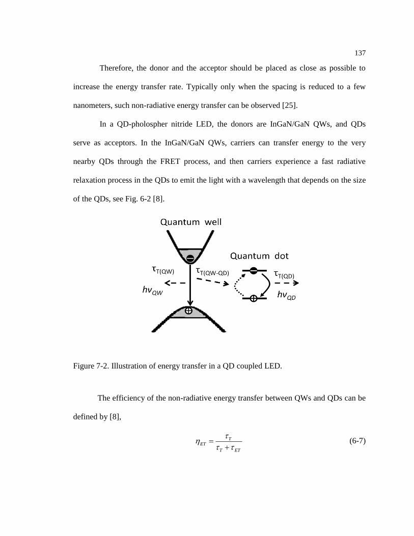
137
Therefore, the donor and the acceptor should be placed as close as possible to
increase the energy transfer rate. Typically only when the spacing is reduced to a few
nanometers, such non-radiative energy transfer can be observed [25].
In a QD-pholospher nitride LED, the donors are InGaN/GaN QWs, and QDs
serve as acceptors. In the InGaN/GaN QWs, carriers can transfer energy to the very
nearby QDs through the FRET process, and then carriers experience a fast radiative
relaxation process in the QDs to emit the light with a wavelength that depends on the size
of the QDs, see Fig. 6-2 [8].
Figure 7-2. Illustration of energy transfer in a QD coupled LED.
The efficiency of the non-radiative energy transfer between QWs and QDs can be
defined by [8],
TET
T ET
(6-7)
138
, where T is the relaxation lifetime of excitations in the QWs including both radiative
and nonradiative decaying, and TE is the relaxation lifetime due to the non-radiative
energy transfer from QWs to QDs. From Eq. 6-7, it can be concluded that a low T and a
high TE are desirable for increasing the non-radiative energy transfer efficiency.
While a prolonged TE could be achieved by minimizing the distance between the
QDs and the QWs separation distance, T is mainly determined by the radiative relaxation
lifetime in a spontaneous emission process for a direct semiconductor and can be
expressed as based on Fermi’s golden rule [26]:
2 1
T m g (6-8)
, where m is the optical transition matrix element and g is the density of photon states
which is a function of frequency and direction of the emission light. The optical transition
element is determined by the structure of QWs. By integrating the emitter source into a
resonant microcavity, g could be adjusted and hence T can be tailored. The dependence
of the relaxation lifetime to the presence of a cavity is called Purcell effect [27].
7.3 Device structure and fabrication
InGaN LEDs with non-resonant microcavity structure were designed and
fabricated in order to extend the radiative recombination lifetime of InGaN QWs and
enhance the direct energy transfer efficiency between QWs and semiconductor QDs.
Figure 6-3 shows the structure of the microcavity InGaN/GaN LED with micro-
holes filled with CdSe/ZnS QDs. The microcavity LED epi-wafer is configured with a
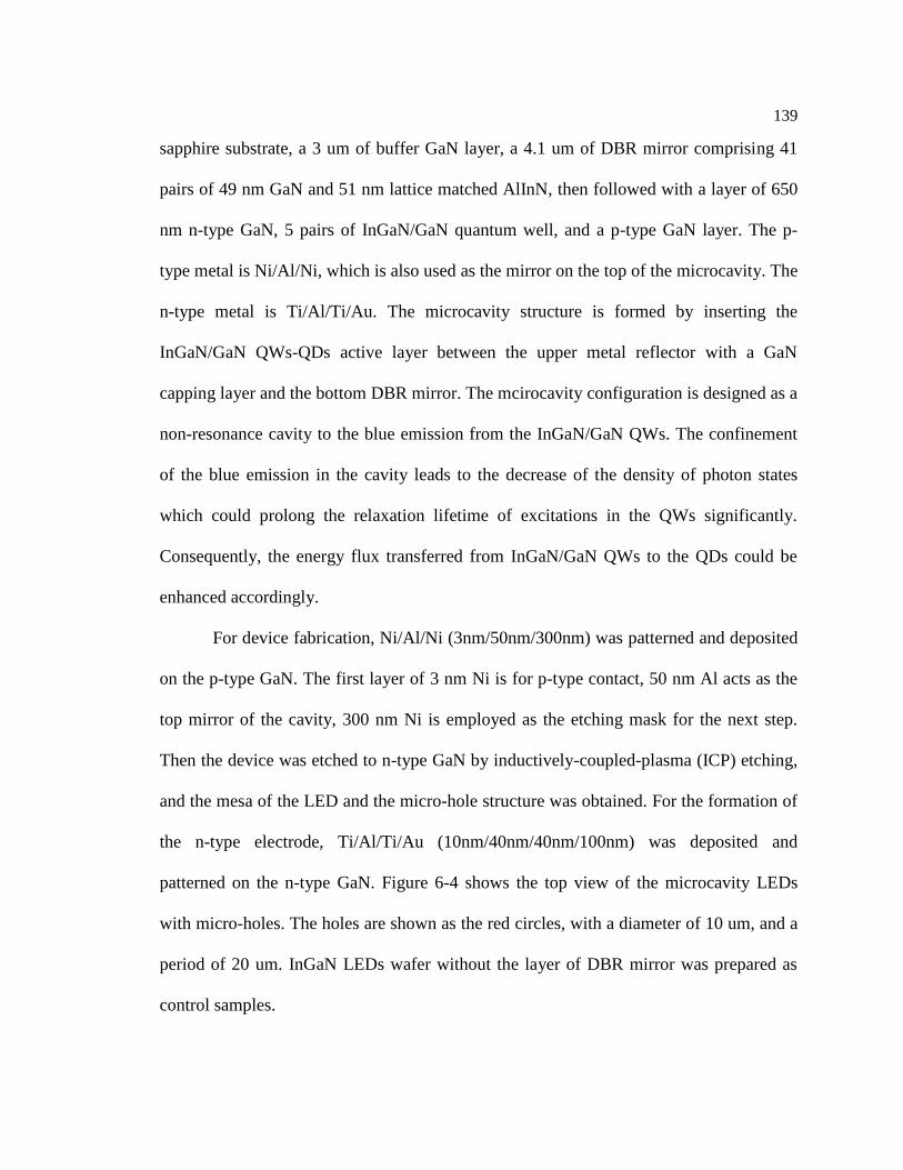
139
sapphire substrate, a 3 um of buffer GaN layer, a 4.1 um of DBR mirror comprising 41
pairs of 49 nm GaN and 51 nm lattice matched AlInN, then followed with a layer of 650
nm n-type GaN, 5 pairs of InGaN/GaN quantum well, and a p-type GaN layer. The p-
type metal is Ni/Al/Ni, which is also used as the mirror on the top of the microcavity. The
n-type metal is Ti/Al/Ti/Au. The microcavity structure is formed by inserting the
InGaN/GaN QWs-QDs active layer between the upper metal reflector with a GaN
capping layer and the bottom DBR mirror. The mcirocavity configuration is designed as a
non-resonance cavity to the blue emission from the InGaN/GaN QWs. The confinement
of the blue emission in the cavity leads to the decrease of the density of photon states
which could prolong the relaxation lifetime of excitations in the QWs significantly.
Consequently, the energy flux transferred from InGaN/GaN QWs to the QDs could be
enhanced accordingly.
For device fabrication, Ni/Al/Ni (3nm/50nm/300nm) was patterned and deposited
on the p-type GaN. The first layer of 3 nm Ni is for p-type contact, 50 nm Al acts as the
top mirror of the cavity, 300 nm Ni is employed as the etching mask for the next step.
Then the device was etched to n-type GaN by inductively-coupled-plasma (ICP) etching,
and the mesa of the LED and the micro-hole structure was obtained. For the formation of
the n-type electrode, Ti/Al/Ti/Au (10nm/40nm/40nm/100nm) was deposited and
patterned on the n-type GaN. Figure 6-4 shows the top view of the microcavity LEDs
with micro-holes. The holes are shown as the red circles, with a diameter of 10 um, and a
period of 20 um. InGaN LEDs wafer without the layer of DBR mirror was prepared as
control samples.
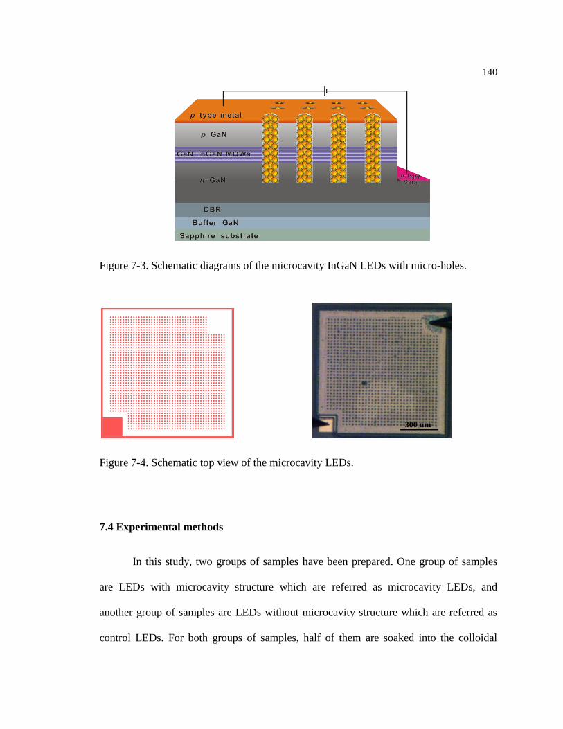
140
Figure 7-3. Schematic diagrams of the microcavity InGaN LEDs with micro-holes.
Figure 7-4. Schematic top view of the microcavity LEDs.
7.4 Experimental methods
In this study, two groups of samples have been prepared. One group of samples
are LEDs with microcavity structure which are referred as microcavity LEDs, and
another group of samples are LEDs without microcavity structure which are referred as
control LEDs. For both groups of samples, half of them are soaked into the colloidal
300 μm
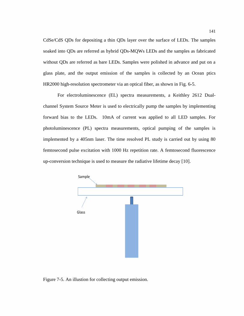
141
CdSe/CdS QDs for depositing a thin QDs layer over the surface of LEDs. The samples
soaked into QDs are referred as hybrid QDs-MQWs LEDs and the samples as fabricated
without QDs are referred as bare LEDs. Samples were polished in advance and put on a
glass plate, and the output emission of the samples is collected by an Ocean ptics
HR2000 high-resolution spectrometer via an optical fiber, as shown in Fig. 6-5.
For electroluminescence (EL) spectra measurements, a Keithley 2612 Dual-
channel System Source Meter is used to electrically pump the samples by implementing
forward bias to the LEDs. 10mA of current was applied to all LED samples. For
photoluminescence (PL) spectra measurements, optical pumping of the samples is
implemented by a 405nm laser. The time resolved PL study is carried out by using 80
femtosecond pulse excitation with 1000 Hz repetition rate. A femtosecond fluorescence
up-conversion technique is used to measure the radiative lifetime decay [10].
Figure 7-5. An illustion for collecting output emission.
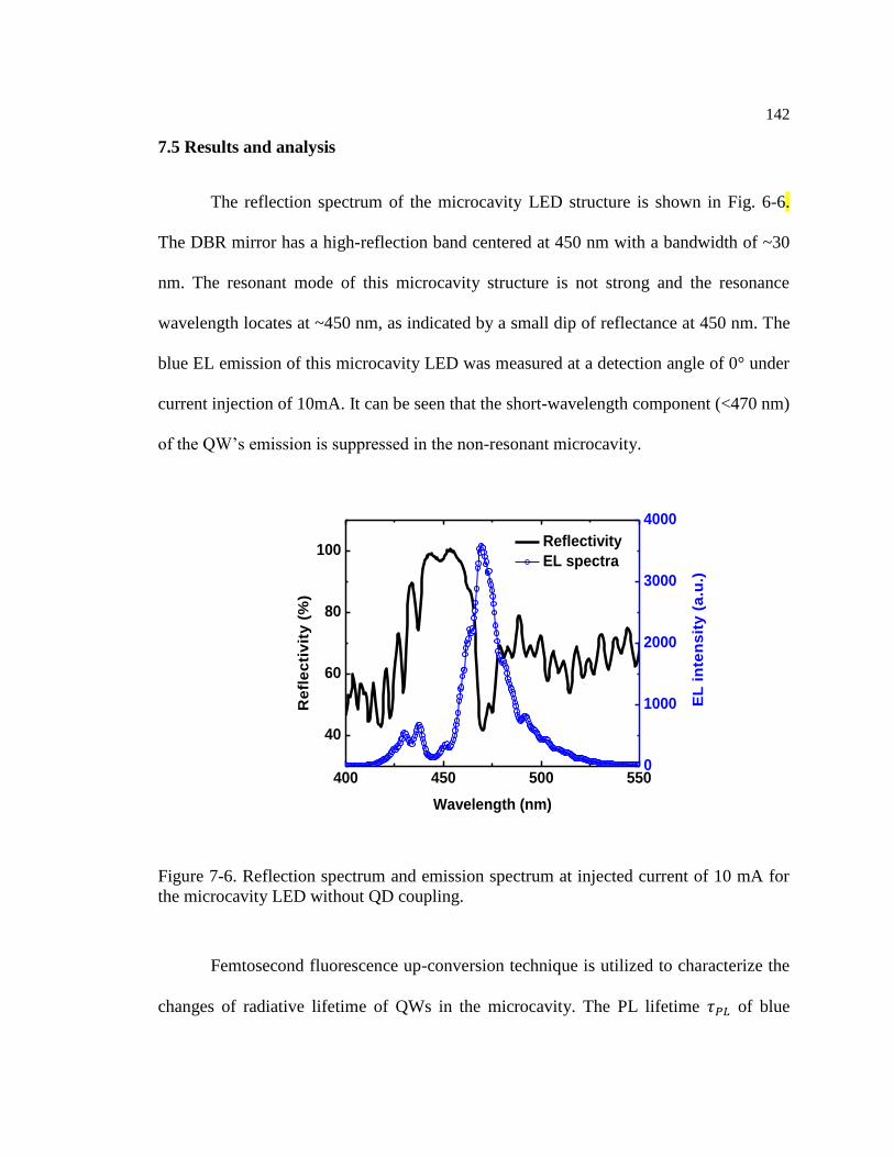
142
7.5 Results and analysis
The reflection spectrum of the microcavity LED structure is shown in Fig. 6-6.
The DBR mirror has a high-reflection band centered at 450 nm with a bandwidth of ~30
nm. The resonant mode of this microcavity structure is not strong and the resonance
wavelength locates at ~450 nm, as indicated by a small dip of reflectance at 450 nm. The
blue EL emission of this microcavity LED was measured at a detection angle of 0° under
current injection of 10mA. It can be seen that the short-wavelength component (<470 nm)
of the QW’s emission is suppressed in the non-resonant microcavity.
400 450 500 550
40
60
80
100 Reflectivity
EL spectra
EL
in
ten
sit
y (
a.u
.)
Re
fle
cti
vit
y (
%)
Wavelength (nm)
0
1000
2000
3000
4000
Figure 7-6. Reflection spectrum and emission spectrum at injected current of 10 mA for
the microcavity LED without QD coupling.
Femtosecond fluorescence up-conversion technique is utilized to characterize the
changes of radiative lifetime of QWs in the microcavity. The PL lifetime of blue
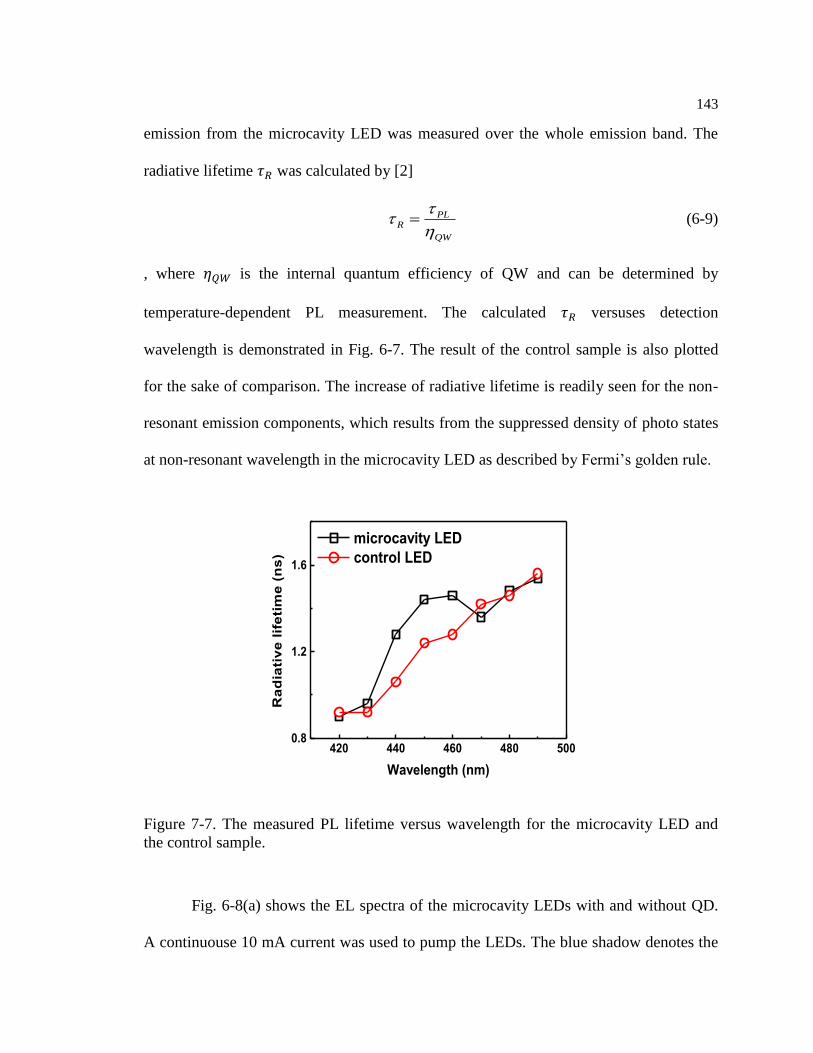
143
emission from the microcavity LED was measured over the whole emission band. The
radiative lifetime was calculated by [2]
PLR
QW
(6-9)
, where is the internal quantum efficiency of QW and can be determined by
temperature-dependent PL measurement. The calculated versuses detection
wavelength is demonstrated in Fig. 6-7. The result of the control sample is also plotted
for the sake of comparison. The increase of radiative lifetime is readily seen for the non-
resonant emission components, which results from the suppressed density of photo states
at non-resonant wavelength in the microcavity LED as described by Fermi’s golden rule.
420 440 460 480 5000.8
1.2
1.6
microcavity LED
control LED
Ra
dia
tiv
e l
ife
tim
e (
ns
)
Wavelength (nm)
Figure 7-7. The measured PL lifetime versus wavelength for the microcavity LED and
the control sample.
Fig. 6-8(a) shows the EL spectra of the microcavity LEDs with and without QD.
A continuouse 10 mA current was used to pump the LEDs. The blue shadow denotes the
144
blue emission from the QW that absorbed by the QDs, and the red shadow denotes the
red emission from the QDs.
The effective internal quantum efficiency of QD emission is defined as [10]
QW QD
QD
QD QW QW QD
QW
N
N N
(6-11)
, where
is the part of the blue emission that does not absorbed by the QDs,
is the QD red emission and is the emission of the LEDs without QD
deposition. For the QD coated microcavity structure, was calculated to be ~47.3%.
Fig. 6-8(b) shows the EL spectra of the control LEDs with and without QD. The
effective internal quantum efficiency of the control sample was calculated to be
~14.7%. The effective quantum efficiency of the QD emission coupled in LEDs with
microcavity structure is 3.2 times higher than the one in LEDs without microcavity
structure. The increase of the effective quantum efficiency should be attributed to the
energy transfer between QWs and QDs, because the two type of samples have the same
QW structures.
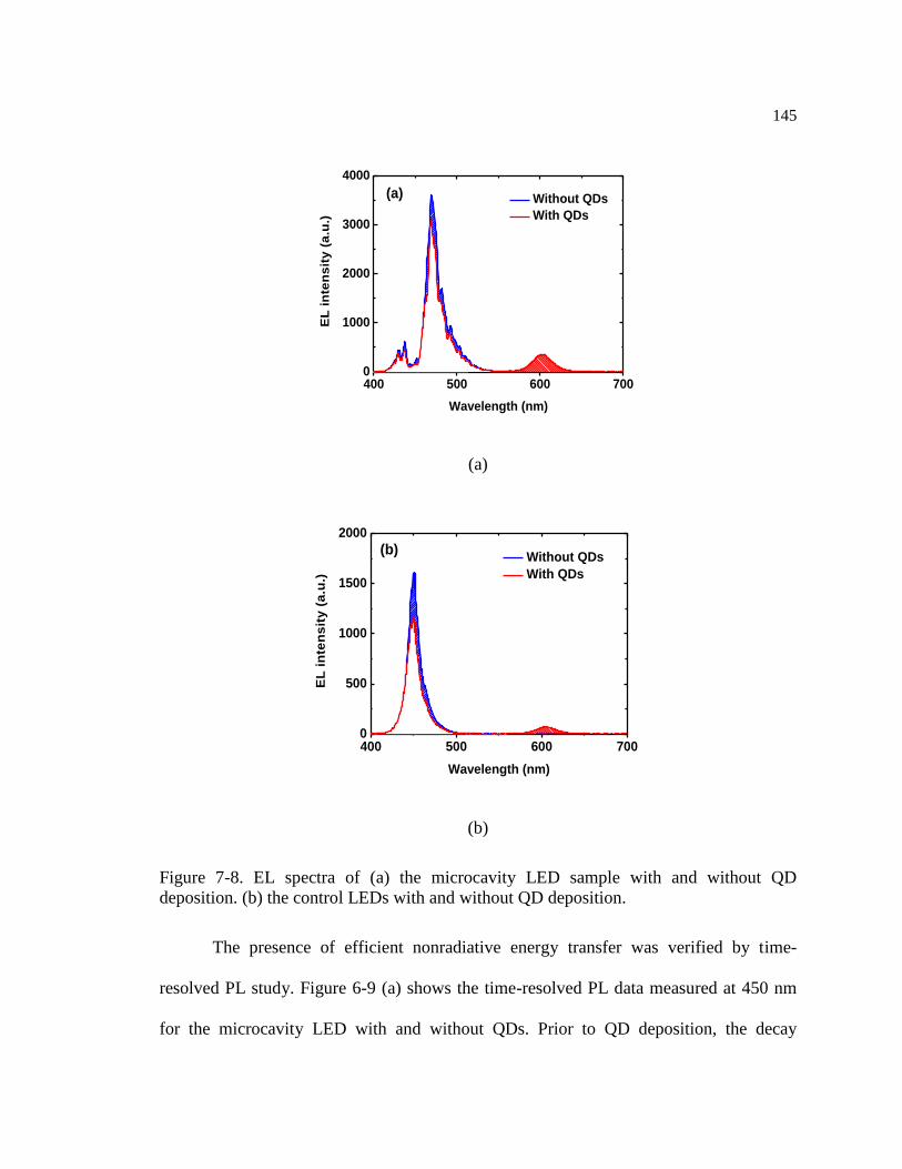
145
400 500 600 7000
1000
2000
3000
4000
Without QDs
With QDs
EL
in
ten
sit
y (
a.u
.)
Wavelength (nm)
(a)
(a)
400 500 600 7000
500
1000
1500
2000
Without QDs
With QDs
EL
in
ten
sit
y (
a.u
.)
Wavelength (nm)
(b)
(b)
Figure 7-8. EL spectra of (a) the microcavity LED sample with and without QD
deposition. (b) the control LEDs with and without QD deposition.
The presence of efficient nonradiative energy transfer was verified by time-
resolved PL study. Figure 6-9 (a) shows the time-resolved PL data measured at 450 nm
for the microcavity LED with and without QDs. Prior to QD deposition, the decay
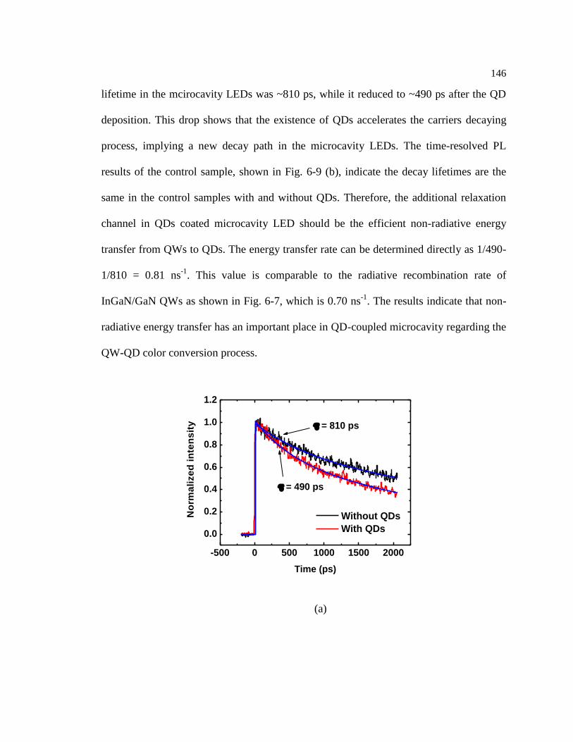
146
lifetime in the mcirocavity LEDs was ~810 ps, while it reduced to ~490 ps after the QD
deposition. This drop shows that the existence of QDs accelerates the carriers decaying
process, implying a new decay path in the microcavity LEDs. The time-resolved PL
results of the control sample, shown in Fig. 6-9 (b), indicate the decay lifetimes are the
same in the control samples with and without QDs. Therefore, the additional relaxation
channel in QDs coated microcavity LED should be the efficient non-radiative energy
transfer from QWs to QDs. The energy transfer rate can be determined directly as 1/490-
1/810 = 0.81 ns-1
. This value is comparable to the radiative recombination rate of
InGaN/GaN QWs as shown in Fig. 6-7, which is 0.70 ns-1
. The results indicate that non-
radiative energy transfer has an important place in QD-coupled microcavity regarding the
QW-QD color conversion process.
-500 0 500 1000 1500 2000
0.0
0.2
0.4
0.6
0.8
1.0
1.2
= 810 ps
Without QDs
With QDs
No
rma
lize
d i
nte
ns
ity
Time (ps)
= 490 ps
(a)
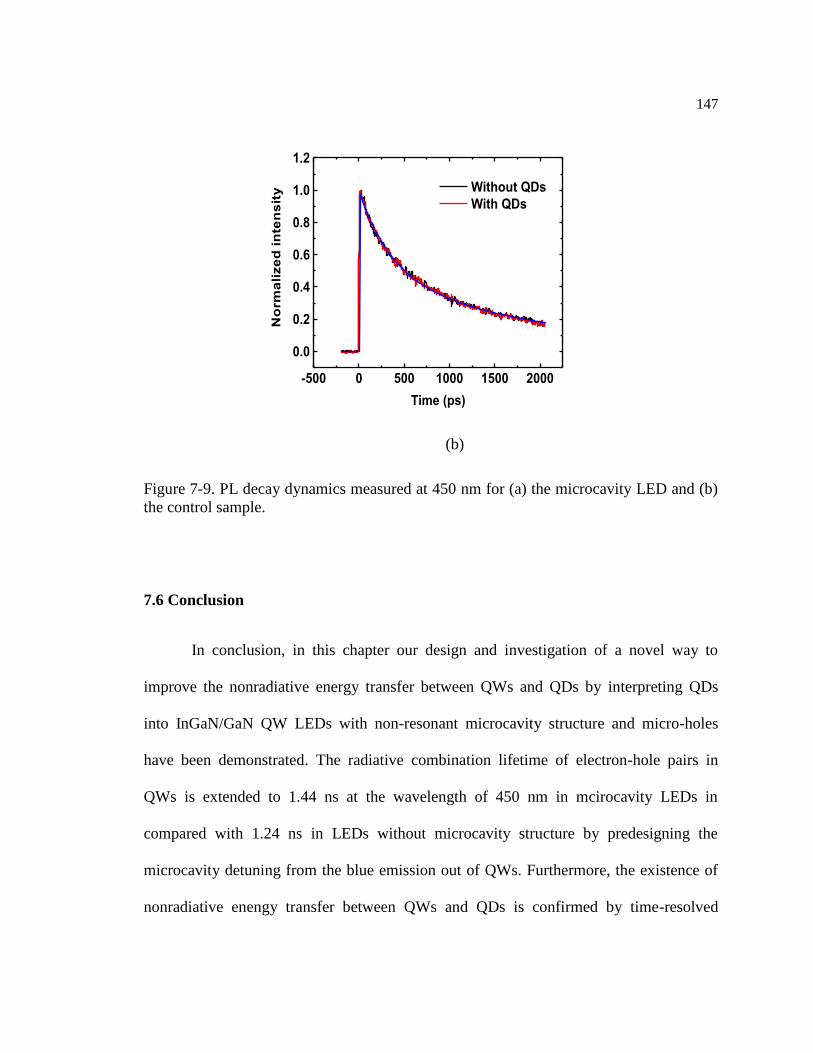
147
-500 0 500 1000 1500 2000
0.0
0.2
0.4
0.6
0.8
1.0
1.2
Without QDs
With QDs
No
rma
lize
d i
nte
ns
ity
Time (ps)
(b)
Figure 7-9. PL decay dynamics measured at 450 nm for (a) the microcavity LED and (b)
the control sample.
7.6 Conclusion
In conclusion, in this chapter our design and investigation of a novel way to
improve the nonradiative energy transfer between QWs and QDs by interpreting QDs
into InGaN/GaN QW LEDs with non-resonant microcavity structure and micro-holes
have been demonstrated. The radiative combination lifetime of electron-hole pairs in
QWs is extended to 1.44 ns at the wavelength of 450 nm in mcirocavity LEDs in
compared with 1.24 ns in LEDs without microcavity structure by predesigning the
microcavity detuning from the blue emission out of QWs. Furthermore, the existence of
nonradiative enengy transfer between QWs and QDs is confirmed by time-resolved
148
photoluminescence study and an enhancement in the effective quantum efficiency is
observed in the LEDs with microcavity structure.
149
Reference
1. Mehta, R. Deshpande, D., Kulkarni, K., Sharma, S., Divan, D., LEDs A
Competitive Solution for General Lighting Applications, Energy 2030
Conference, 2008. ENERGY 2008. IEEE, 17-18 Nov. 2008, 1 - 5.
2. Michael R. Krames, Oleg B. Shchekin, Regina Mueller-Mach, Gerd O. Mueller,
Ling Zhou, Gerard Harbers, and M. George Craford, Status and Future of High-
Power Light-Emitting Diodes for Solid-State Lighting, JOURNAL OF DISPLAY
TECHNOLOGY, VOL. 3, NO. 2, JUNE 2007.
3. U.S. Department of Energy, Energy Savings Potential of Solid-State Lighting in
General Illumination Applications, (2012).
4. Linda Sivertsen, Tosh Sivertsen, Generation Green: The Ultimate Teen Guide to
Living an Eco-Friendly Life, Simon Pulse (August 5, 2008).
5. Pierre Ruterana, Martin Albrecht, Jörg Neugebauer, Nitride Semiconductors:
Handbook on Materials and Devices, Wiley-VCH; 1 edition (June 9, 2003).
6. V. L. COLVIN, M. C. SCHLAMP and A. P. ALIVISATOS, Light-emitting
diodes made from cadmium selenide nanocrystals and a semiconducting polymer,
Nature 370, 354 - 357 (04 August 1994).
7. Qingjiang Sun, Y. Andrew Wang, Lin Song Li, Daoyuan Wang, Ting Zhu, Jian
Xu, Chunhe Yang and Yongfang Li, Bright, multicoloured light-emitting diodes
based on quantum dots, Nature Photonics 1, 717 - 722 (2007).
8. Marc Achermann, Melissa A. Petruska, Simon Kos, Darry L. Smith, Daniel D.
Koleske and Victor I. Klimov, Energy-transfer pumping of semiconductor
150
nanocrystals using an epitaxial quantum well, Nature 429, 642-646 (10 June
2004).
9. Donald Neamen , “Semiconductor Physics and Devices”, McGraw-Hill, 2011.
10. Fan Zhang, Jie Liu, Guanjun You, Chunfeng Zhang, Suzanne E. Mohney, Min
Joo Park, Joon Seop Kwak, Yongqiang Wang, Daniel D. Koleske, and Jian Xu,
Nonradiative energy transfer between colloidal quantum dot-phosphors and
nanopillar nitride LEDs, Optics Express, Vol. 20, Issue S2, pp. A333-A339
(2012).
11. Marc Achermann , Melissa A. Petruska , Daniel D. Koleske , Mary H. Crawford ,
and Victor I. Klimov, Nanocrystal-Based Light-Emitting Diodes Utilizing High-
Efficiency Nonradiative Energy Transfer for Color Conversion, Nano Lett., 2006,
6 (7), pp 1396–1400.
12. Chanyawadee, Soontorn, Lagoudakis, Pavlos G., Harley, Richard, Charlton,
Martin, Talapin, Dmitri, Huang, Hong Wen and Chung-Hsiang, Lin, Increased
color-conversion efficiency in hybrid light-emitting diodes utilizing non-radiative
energy transfer. Advanced Materials, 22, (5), 602-606.
13. Andrey Rogach, Semiconductor Nanocrystal Quantum Dots: Synthesis,
Assembly, Spectroscopy and Applications, Springer, Sep 2, 2008.
14. Peter YU, Manuel Cardona, Fundamentals of Semiconductors: Physics and
Materials Properties , Springer; 4th ed. 2010 edition (May 17, 2010).
15. David A. B. Miller, Quantum Mechanics for Scientists and Engineers, Cambridge
University Press (April 21, 2008).
151
16. Elias Burstein, Claude Weisbuch, Confined Electrons and Photons: New Physics
and Applications, Springer Science & Business Media, May 31, 1995.
17. Günter Schmid, Nanoparticles: From Theory to Application, Wiley-VCH; 2nd,
Completely Revised and Updated Edition edition (October 4, 2010).
18. C. B. Murray, D. J. Norris , M. G. Bawendi, Synthesis and characterization of
nearly monodisperse CdE (E = sulfur, selenium, tellurium) semiconductor
nanocrystallites, J. Am. Chem. Soc., 1993, 115 (19), pp 8706–8715.
19. Joshua James Angell, SYNTHESIS AND CHARACTERIZATION OF CdSe-ZnS
CORE-SHELL QUANTUM DOTS FOR INCREASED QUANTUM YIELD,
California Polytechnic State University, 2011.
20. Peter Reiss, Myriam Protie`re, and Liang Li, Core/Shell Semiconductor
Nanocrystals, 2009 Wiley-VCH Verlag GmbH & Co. KGaA, Weinheim.
21. Benoit Deveaud, The Physics of Semiconductor Microcavities, John Wiley &
Sons, Feb 27, 2007.
22. E. Fred Schubert, Light-Emitting Diodes, Cambridge University Press, Jun 8,
2006.
23. Orazio Svelto, Principles of Lasers, Springer Science & Business Media, Mar 16,
2010.
24. Igor Medintz and Niko Hildebrandt, FRET - Förster Resonance Energy Transfer:
From Theory to Applications, John Wiley & Sons, Oct 4, 2013.
25. Manuela Lunz, A. Louise Bradley, Valerie A. Gerard, Stephen J. Byrne, Yurii K.
Gun’ko, Vladimir Lesnyak, and Nikolai Gaponik, Concentration dependence of
152
Förster resonant energy transfer between donor and acceptor nanocrystal quantum
dot layers: Effect of donor-donor interactions, Phys. Rev. B 83, 115423.
26. Malte Huck, Optical and Electrical Properties of Single Self-Assembled Quantum
Dots in Lateral Electric Fields, diplom.de, Mar 24, 2010.
27. Mark Fox, Quantum Optics: An Introduction: An Introduction, Oxford University
Press (June 22, 2006).
28. Raymond A. Serway, John W. Jewett, Physics for Scientists and Engineers,
Volume 2, Cengage Learning; 9 edition (December 19, 2012).
29. Shuji Nakamura and Michael R. Krames, “History of Gallium–Nitride-Based
Light-Emitting Diodes for Illumination”, Proceedings of the IEEE, Vol. 101, No.
10, October 2013.
153
Chapter 8
Future Work
8.1 Chip-level integration of gallium nitride light emitting diodes and vertical metal
semiconductor field effect transistors
Based on our study of the GaN SBDs fabricated on LED epi-wafers, a monolithic
integration of GaN LEDs and vertical metal-semiconductor field effect transistors
(MESFETs) can be achieved, as shown in Fig. 8-1. Selective regions of n-type doped
GaN surface or unintentionally doped GaN surface will be exposed by etching, and a
sufficient thin vertical conductive channel which also is an n-type doped GaN mesa will
be formed. Top ohmic contact on n-type doped GaN layer will be the drain terminal, and
bottom ohmic contact on unintentionally doped GaN layer will be the source terminal.
The gate Schottky metal will be deposite on the uninterntionally doped GaN layer and
surround the vertical channel. A negative gate bias should be applied to pinch off the
current flowing. The MESFET-integrated GaN LEDs are expected to extend the potential
intelligent lighting applications of GaN LEDs in the future.
154
Figure 8-1. The monolithic integration of a GaN LED and a vertical MESFET.
8.2 Monolithic integration of LEDs and AlInN/GaN HEMTs
In this work, we will use re-growth methord to realize the monolithic integration
of GaN LEDs and AlInN/GaN HEMTs. The re-growth methord can remove the plasma
damage in the integration processes. Moreover, the lattice-matched AlInN/GaN HEMTs
can potentially provide higher output current and have improved stability and reliability
compared to AlGaN/GaN HEMTs.
155
Figure 8-2. The monolithic integration of a GaN LED and a AlInN/GaN HEMT.
VITA
Li Wang
EEDDUUCCAATTIIOONN
Ph.D. Department of Engineering Science and Mechanics 08/2010~5/2015
The Pennsylvania State University, University Park, PA, USA
M.S. Department of Electronic Engineering 09/2007~07/2010
Tsinghua University, Beijing, P.R. China
B.S. Department of Communications Engineering 09/2003~07/2007
Communication University of China, Beijing, P.R. China
SSEELLEECCTTEEDD PPUUBBLLIICCAATTIIOONNSS
[1] Li Wang, Xuefeng Zhang, Guanjun You, Feng Xiong, Lixin Liang, Yong Hu, Aping
Chen, Jie Liu and Jian Xu, "Modeling the back gate effects of AlGaN/GaN HEMTs,"
Journal of Computational Electronics, August 7, 2014.
[2] Xue Feng Zhang, Lai Wei, Li Wang, Jie Liu, and Jian Xu, "Gate length related
transfer characteristics of GaN-based high electron mobility transistors," Applied Physics
Letters, 102, 113501, 2013.
[3] Zhang Xue-Feng, Wang Li, Liu Jie, Wei Lai, Xu Jian, "Electrical characteristics of
AlInN/GaN HEMTs under cryogenic operation," Chin. Phys. B 2013, Vol. 22 Issue (1):
017202.
[4] Li Wang, Wenhua Chen, Peng Wang, Xin Xue, Jiaxing Dong and Zhenghe Feng,
"Design of asymmetrical spurline filter for a high power sic MESFET class-E power
amplifier," Microwave and Optical Technology Letters, v 52, n 7, p 1650-2, July 2010.
[5] Li Wang, Wenhua Chen, Peng Wang, Xin Xue, Jiaxing Dong and Zhenghe Feng, “A
High Power SiC MESFET Class-E Power Amplifier With An Asymmetrical Spurline
Resonator,” Asia-Pacific Microwave Conference, 2009, p 1120-3, 2009.

![Nanocrystalline Aluminum Nitride and Aluminum/Gallium Nitride Nanocomposites via Transamination of [M(NMe 2 ) 3 ] 2 , M = Al, Al/Ga (1/1)](https://img.pdfslide.net/doc/110x75/6362d1e5ca50a88b570430b4/nanocrystalline-aluminum-nitride-and-aluminumgallium-nitride-nanocomposites-via.jpg)


![SPIE Proceedings [SPIE SPIE OPTO - San Francisco, California, USA (Saturday 2 February 2013)] Gallium Nitride Materials and Devices VIII - Recombination dynamics in non-polar m-plane](https://img.pdfslide.net/doc/110x75/63505dc0d2282bdce30f1c94/spie-proceedings-spie-spie-opto-san-francisco-california-usa-saturday-2-february.jpg)


