Embed Size (px)
Citation preview

Gate-Tunable Resonant Tunneling in Double Bilayer
Graphene Heterostructures
Babak Fallahazad‡, Kayoung Lee‡, Sangwoo Kang‡, Jiamin Xue, Stefano Larentis, Christopher
Corbet, Kyounghwan Kim, Hema C. P. Movva, Takashi Taniguchi a)
, Kenji Watanabe a)
,
Leonard F. Register, Sanjay K. Banerjee, Emanuel Tutuc*
Microelectronics Research Center, Department of Electrical and Computer Engineering,
The University of Texas at Austin, Austin, TX 78758, USA
a) National Institute for Materials Science, 1-1 Namiki Tsukuba Ibaraki 305-0044, Japan
Keywords: Bilayer graphene, hexagonal boron nitride, heterostructure, resonant
tunneling, negative differential resistance, tunneling field-effect transistor.
Abstract: We demonstrate gate-tunable resonant tunneling and negative differential
resistance in the interlayer current-voltage characteristics of rotationally aligned double bilayer
graphene heterostructures separated by hexagonal boron-nitride (hBN) dielectric. An analysis of
the heterostructure band alignment using individual layer densities, along with experimentally
determined layer chemical potentials indicates that the resonance occurs when the energy bands
of the two bilayer graphene are aligned. We discuss the tunneling resistance dependence on the
interlayer hBN thickness, as well as the resonance width dependence on mobility and rotational
alignment.

Recent progress in realization of atomically thin heterostructures by stacking two-
dimensional (2D) atomic crystals, such as graphene, hexagonal boron nitride (hBN), and
transition metal dichalcogenides (TMDs) has provided a versatile platform to probe new physical
phenomena, and explore novel device functionalities [1], [2]. Combining such materials in
vertical heterostructures may provide new insight into the electron physics in these materials
through Coulomb drag [3], [4] or tunneling [5], [6]. Tunneling between two distinct 2D carrier
systems, namely 2D-2D tunneling has been used in GaAs 2D electron [7], [8] and 2D hole
systems [9]-[11] as a technique to probe the Fermi surface and quasi-particle lifetime. When the
energy bands of two parallel 2D carrier systems are energetically aligned, momentum conserving
tunneling leads to a resonantly enhanced tunneling conductivity and negative differential
resistance (NDR).
The emergence of single or few atom-thick semiconductors, such as graphene and TMDs
can open new routes to probe 2D-2D tunneling in their heterostructures, which in turn may
enable new device applications [5], [12], [13]. While fascinating, resonant tunneling between
two graphene or TMD layers realized using a layer-by-layer transfer approach is experimentally
challenging because the energy band minima are located at the K points in the first Brillouin
zone, and the large K-point momenta coupled with small rotational misalignment between the
layers can readily obscure resonant tunneling.
Bilayer graphene consists of two monolayer graphene in Bernal stacking, and has a
hyperbolic energy-momentum dispersion with a tunable bandgap [14]–[16]. Hexagonal boron-
nitride is an insulator with an energy gap of 5.8 eV [17] and dielectric strength of 0.8 V/nm [18],

which has emerged as the dielectric of choice for graphene [1] thanks to its atomically flat, and
chemically inert surface. We demonstrate here resonant tunneling and NDR between two bilayer
graphene flakes separated by an hBN dielectric. A detailed analysis of the band alignment in the
heterostructure indicates that the NDR occurs when the charge neutrality points of the two layers
are energetically aligned, suggesting momentum conserving tunneling is the mechanism
responsible for the resonant tunneling.
Figure 1a shows a schematic representation of our double bilayer heterostructure devices,
consisting of two bilayer graphene flakes separated by a thin hBN layer. The devices are
fabricated through a sequence of bilayer graphene and hBN mechanical exfoliation, alignment,
dry transfers, e-beam lithography, and plasma etching steps similar to the techniques reported in
Refs. [1], [19]–[21] (supporting information). The bilayer graphene flakes selected for the device
fabrication have at least one straight edge which is used as a reference to align the crystalline
orientation of the bottom and top bilayer graphene during the transfer (Fig. 1b). The accuracy of
the rotational alignment is mainly limited by the size of the flakes, and the resolution of the
optical microscope. For a typical length of the bilayer graphene straight edge of 10 – 20 µm, we
estimate the rotational misalignment between the two bilayers in our devices to be less than 3
degrees. The interlayer hBN straight edges are not intentionally aligned with either the top or
bottom graphene layers during transfers.
The interface between various materials in an atomically thin heterostructure plays a key
role in device quality and tunneling uniformity. Particularly, the presence of contaminants, such
as tape or resist residues, and wrinkles in the tunneling region and in between the layers changes
the interlayer spacing and the local carrier density, which in turn makes the tunneling current
distribution non-uniform. To achieve an atomically flat interface with minimum contamination,

the heterostructure is annealed either after each transfer or after the stack completion in high
vacuum (10-6
Torr), at a temperature T = 340C for 8 hours. Figure 1c depicts the optical
micrograph of the final device where the bottom and top bilayer graphene boundaries are marked
by red and yellow dashed lines; the interlayer hBN is not visible in this micrograph. The devices
are characterized at temperatures ranging from T = 1.4 K to room temperature, using small
signal, low frequency lock-in techniques to probe the individual layer resistivities, and a
parameter analyzer for the interlayer current-voltage characteristics. Eight devices were
fabricated and investigated in this study; we focus here on data from three devices, labelled #1,
#2, and #3. Device #1 consists of the double bilayer heterostructure separated by hBN where the
top layer is exposed to ambient, while Devices #2 and #3 have the top layer capped with an
additional hBN layer. The interlayer dielectric thickness of Devices #1, #2, and #3 correspond to
six, five, and four hBN monolayers, respectively.
To characterize the double bilayer system, it is instructive to start with the characteristics
of the individual layers. The device layout allows us to independently probe the bottom and top
layer resistivites (ρB, ρT), and carrier densities (nB, nT) in the overlap (tunneling) region as a
function of the back-gate (VBG) and interlayer bias (VTL) applied on the top layer; the bottom
layer potential is kept at ground during all measurements. Figure 2 shows the bottom (panel a)
and top (panel b) layer resistivity measured as a function of VBG and VTL in Device #1, at T = 1.4
K. The carrier mobility of Device #1 measured from the four-point conductivity is 150,000 -
160,000 cm2/V·s for the bottom bilayer and 3,500 cm
2/V·s for the top bilayer at T = 1.4 K. The
data of Fig. 2 indicate that the combination of gate biases at which both bilayer graphene are
charge neutral, namely the double charge neutrality point (DNP), is: VBG-DNP = 20.2 V and VTL-
DNP = -0.235 V.
At a given set of VBG and VTL, the values of nB and nT can be calculated using the
following equations [22]:
岫弔 − 弔−帖岻 = 態岫券 + 券脹岻系弔 + 航 岫な岻岫脹 − 脹−帖岻 = − 態券脹系津 + 航 − 航脹 岫に岻
Here e is the electron charge, CBG is the back-gate capacitance, Cint is the interlayer dielectric
capacitance, 航脹 and 航 are the top and bottom bilayer graphene chemical potential measured
with respect to the charge neutrality point, respectively. Solving eqs. 1 and 2 yields a one-to-one
correspondence between the applied biases and the layer densities. Finding a self-consistent
solution for eqs. 1 and 2 requires the CBG and Cint values, and the layer chemical potential
dependence on carrier density. We discuss in the following an experimental method to
determine the capacitance values in a double bilayer graphene, along with the chemical potential
dependence on the carrier density.
Along the charge neutrality line (CNL) of the top bilayer graphene [i.e. 券脹 = 航脹 = ど],
eq. 2 reduces to 航 = 岫脹 − 脹−帖岻, thus the 航 value at a given VBG can be determined
along the top layer CNL. To determine the value of the CBG, we measure ρB and ρT of the device
in a perpendicular magnetic field. Figure 3a presents the ρT contour plot of Device #1 measured
as a function of VBG and VTL, in a perpendicular magnetic field B = 13 T, and at T = 1.5 K. The
charge neutrality line of the top bilayer graphene (dashed line in Fig. 3a) shows a staircase
behavior, which stems from the bottom bilayer graphene chemical potential crossing the Landau
levels (LLs) [19]. At a given LL filling factor (ν), marked in Fig. 3a, the bottom bilayer

graphene carrier density is 券 = 荒稽 ℎ⁄ ; h is the Planck constant. Writing eqs. 1 and 2 along the
top bilayer CNL, combined with 券 = 荒稽 ℎ⁄ yields:
系弔 = 態稽ℎ 峭∆岫弔 − 脹岻∆荒 嶌−怠 岫ぬ岻
Where ∆岫弔 − 脹岻 is the change in 弔 − 脹 corresponding to a bottom bilayer filling factor
change ∆荒 along the top layer CNL (dashed line in Fig. 3a). Figure 3b shows a clear linear
dependence of 岫弔 − 脹岻 vs. ν, marked by circles in Fig. 3a. The slope of 岫弔 − 脹岻 vs. ν
data along with eq. 3 yields CBG = 10.5 nF/cm2 for Device #1, corresponding to 285 nm-thick
SiO2 in series with 40 nm-thick hBN dielectric.
The nB value along the top bilayer CNL can be calculated using eqs. 1 and 2:
券 = 系弔 ∙ [岫弔 − 弔−帖岻 − 岫脹 − 脹−帖岻] 岫ね岻
Combining the µB values determined along the top layer CNL of Fig. 2b, with eq. 4 yields µB vs.
nB. Figure 3c shows µB vs. nB for Devices #1 and #3. We note that in addition to the layer
densities, the applied VBG and VTL also change the transverse electric fields across the two layers
(see supporting information). The chemical potential of the two devices match well at high
carrier densities, but differ near nB = 0 thanks to different transverse electric fields values across
the bottom layer near the DNP [14]. Because the experimental data show the bilayer graphene
chemical potential is weakly dependent on the transverse electric fields away from the neutrality
point, and to simplify the solution of eqs. 1 and 2 we neglect the 航脹 and 航 dependence on the
transverse electric field across the individual layers. The dashed line in the Fig. 3c depicts a

polynomial fit to the experimental 航 vs. 券 data, which will be subsequently used to solve eqs.
1 and 2.
We now turn to the extraction of the Cint value. Let us consider the bottom bilayer
graphene CNL, marked by a dashed line in Fig. 2a. In a dual gated graphene device with
metallic gates, the value of the top-gate capacitance can be readily extracted from the linear shift
of the bottom graphene charge neutrality point with back-gate and top-gate voltages [23], which
yields the top-gate to back-gate capacitance ratio. Because the top layer is not a perfect metal,
using the slope of the bottom bilayer CNL of Fig. 2a to calculate Cint neglects the contribution of
the top bilayer quantum capacitance. Combining eqs. 1 and 2 along the bottom bilayer CNL, i.e. 券 = 航 = ど, we obtain the following expression that includes the quantum capacitance: 系津 = − 系弔 ∙ 岫弔 − 弔−帖岻岫脹 − 脹−帖岻 + 航脹岫系弔 ∙ 岫弔 − 弔−帖岻/岻 岫の岻
Using eq. 5 and the 航脹 vs. n dependence of Fig. 3c, we determine an interlayer dielectric
capacitance of Cint = 1.02 µF/cm2 for Device #1. The Cint values for Devices #2, and #3 are 1.23
µF/cm2, and 1.55 µF/cm
2, respectively.
Now we turn to the interlayer current (Iint) - voltage characteristics of our devices. Figure
4a shows the Iint vs. VTL for Device #1 measured at various VBG values, and at T = 10 K. For
small bias values, Iint increases monotonically with VTL, corresponding to an interlayer resistance
of 39 GΩ·µm2. For VBG values ranging from 10 V to 30 V, the interlayer current-voltage traces
show a marked resonance and NDR, which depend on the applied VBG. Figure 4b presents the Iint
vs. VTL of Device #2 measured at room temperature. The normalized interlayer resistance of
Device #2 at the limit of VTL = 0 V is 1 GΩ·µm2. Similar to the Device #1 data, we observe

resonant tunneling and NDR in the interlayer current-voltage characteristics. A distinct
difference between the two devices is that the resonance is centered around VTL = 0 V in Device
#2 by comparison to Device #1. As we discuss below, the NDR position can be explained
quantitatively by considering the electrostatic potential across the double bilayer
heterostructures.
Figure 4c shows the normalized interlayer resistance (Rc) in double bilayer graphene
devices as a function of interlayer hBN thickness, from 4 to 8 monolayers, measured at zero
interlayer bias, and at either low T = 1.4 - 20 K temperatures, or at room temperature. Data are
included from both devices with and without resonant tunneling. The data show an exponential
dependence on thickness of the tunneling barrier, similar to experimental tunneling data through
hBN using graphite and gold electrodes [24]. These data indicate that the Rc value is largely
determined by the interlayer hBN thickness.
To better understand the origin of the observed NDR in Figs. 4a and 4b, it is instructive
to examine the energy band alignment in the double bilayer graphene heterostructure. To
determine if the NDR occurrence stems from momentum conserving tunneling, we examine the
biasing conditions at which the charge neutrality points of the two bilayer graphene are aligned
and the electrostatic potential drop across the interlayer dielectric is zero:
脹 + 航脹岫券脹岻 − 航岫券岻 = ど 岫は岻
Figure 5a illustrates the energy band alignment of a double bilayer graphene device at
biasing conditions where the charge neutrality points of top and bottom bilayers are aligned, the
condition most favorable for momentum conserving tunneling. The schematic ignores the band-
gap induced in the two layers as a result of finite transverse electric fields (see supporting

information), as the layer chemical potentials are controlled mainly by the carrier densities (Fig.
3c). The symbols in Fig. 5b show the experimental values of the tunneling resonance as a
function of VTL and VBG for Devices #1 and #2, defined as the maximum conductivity point in
Fig. 4a,b data. The solid lines show the calculated VTL vs. VBG values corresponding to layer
densities and chemical potential that satisfy eq. 6, corresponding to the charge neutrality points
of the two layers being aligned. The good agreement between the experimental values and
calculations in Fig. 5b strongly suggests that the tunneling resonance occurs when the charge
neutrality points of the two bilayer graphene are aligned, which in turn maximizes momentum
(k) conserving tunneling between the two layers [25]–[27]. This observation is also in
agreement with the findings in other 2D-2D systems where resonant tunneling occurs when the
energy bands of the two quantum wells are aligned [8]–[11]. We note however, that in addition
to the tunneling resonances, both devices exhibit a non-resonant tunneling current background
which increases with VTL, associated with non-momentum-conserving tunneling. This non-
resonant tunneling component has a weak temperature dependence, which implies it is not
caused by phonon assisted tunneling or thermionic emission.
Figure 5c shows the layer densities 券脹 vs. 券 calculated in Devices #1 and #2 at the
tunneling resonance position corresponding to Figs. 4a,b data. In Device #1 the top (bottom)
bilayer is populated with holes (electrons) at the tunneling resonance. In Device #2 the top
bilayer is close to neutrality, while the bottom bilayer carrier type can be either hole or electron
depending on the applied VBG. Most notably, in both devices the tunneling resonance occurs at a
fixed top layer density value. This observation can be understood using eq. 2 and eq. 6, which
yield a fixed top layer density 券脹 = 岫脹−帖 ∙ 系津岻 ⁄ when the charge neutrality points are
aligned, independent of VBG.

In addition to the location of the resonances, we also considered their broadening.
Potential sources of broadening include finite initial and final state lifetimes due to scattering,
rotational misalignment θ, or the non-uniformity of tunneling associated with spatial
inhomogeneities. While a detailed theoretical description of the tunneling in double bilayers is
outside the scope of this study, in the following we provide estimates for the broadening
associated with these mechanisms gauges in terms of the alignment of the band structures, i.e.,
the electrostatic potential difference between bilayers 帳聴 = 脹 + [航脹岫券脹岻 − 航岫券岻]/.
The contribution from the carrier scattering lifetime () in either layer to the broadening
width in units of volts is ∆ ≅ ℏ 岫岻⁄ , where ħ is the reduced Planck constant. Using the
momentum relaxation time 陳 obtained from the carrier mobility 航 = 陳 兼∗⁄ , where 兼∗ is the
effective mass, a lower limit of the broadening can be estimated to be ∆ ≅ ℏ 岫航兼∗岻⁄ . The
broadening width associated with rotational misalignment can be estimated using the wave-
vector difference ∆ = ||θ illustrated in Fig. 6b, which translates into a broadening ∆θ ≅ ℏ||θ ⁄ , where is an average velocity of the tunneling carriers, and || = な.ば × など怠待 m-1
is
the wave-vector magnitude at the valley minima. Using the Fermi velocity of monolayer
graphene vF = 1.1108 cm/s as reference leads to a numerical expression ∆θ ≅ 岫になの m岻岫 庁⁄ 岻岫θ なo⁄ 岻. The lower carrier velocity in bilayer by comparison to
monolayer graphene leads to a reduced resonance broadening at a given rotational misalignment
angle θ. Moreover, a smoother resonance broadening shape for rotational misalignment is
expected for the double bilayer graphene thanks to the quasi-parabolic energy-momentum
dispersion, compared to a rotationally misaligned double graphene monolayer [5], [26].

The effective mass of bilayer graphene is both density and transverse electric field
dependent [14], [19]. Using an average effective mass value 兼∗ = ど.どの兼 [19], where me is the
bare electron mass, the lower layer mobility value in Device #1 of 3,500 cm2/V·s corresponds to
a broadening ∆ = ば mV. For Device #2 the corresponding broadening is ∆ = なな mV, using
the top and bottom layer mobility values of 14,800 and 2,400 cm2/V·s, respectively, measured at
room temperature.
The experimental values for the tunneling resonance width are ∆帳聴 ≅ なに mV and ∆帳聴 ≅ ばは mV for Devices #1 and #2, measured at T = 10 K, and room temperature
respectively. These values are determined by fitting Lorentzian peaks to the Iint data of Fig. 4a,b
data plotted as a function of 帳聴; an example is shown in Fig. 6c. Fitting a Lorentzian peak to the 津/脹 vs. 帳聴 data yields very similar ∆帳聴 values. As the ∆ values calculated above are
lower than the experimental values ∆帳聴, we conclude that the broadening is mainly limited by
rotational alignment in our devices, with Device #1 having a better alignment than Device #2.
Although we cannot quantify experimentally the rotational misalignment in the two devices, we
note that during fabrication Device #1 was annealed after each graphene and hBN layer transfer,
while Device #2 was annealed after the double bilayer stack was completed. We speculate that
multiple annealing steps may improve the rotational alignment between the layers.
In summary, we present a study of interlayer electron transport in double bilayer
graphene. In devices where the bilayers straight edges were rotationally aligned during the
fabrication we observe marked resonances in interlayer tunneling. Using individual layer
densities and experimental values of the layer chemical potential we show that the resonances
occur when the charge neutrality points of the two layers are energetically aligned, consistent
with momentum-conserving tunneling. The interlayer conductivity values show an exponential
dependence of the interlayer hBN thickness, and can serve to benchmark switching speed for
potential device applications.

Figure 1. Double bilayer device structure. (a) Schematic of the double bilayer graphene
device. (b) Optical micrograph of the top and bottom graphene flakes illustrating the alignment
of straight edges. The red (yellow) lines mark the boundaries of the bottom (top) bilayer
graphene. (c) Optical micrograph of the device. The red (yellow) dashed lines mark the bottom
(top) bilayer graphene.

Figure 2. Individual layer characterization. Device #1 bottom [panel (a)] and top [panel (b)]
bilayer graphene resistivity contour plots measured as a function of VBG and VTL at T = 1.4 K.
The charge neutrality points in both panels are marked by black dashed lines.

Figure 3. Capacitance and chemical potential measurement. (a) Contour plot of ρT measured
as a function of VBG and VTL, at B = 13 T and T = 1.5 K in Device #1. The bottom bilayer
graphene LL filling factors are marked. (b) 弔 − 脹 vs. 荒 of the bottom bilayer showing a
linear dependence; the 系弔 value is determined from the slope. (c) 航 vs. nB for Devices #1 and
#3. The dashed line is the polynomial fit to the experimental data.

Figure 4. Interlayer current-voltage characteristics and resonant tunneling. Iint vs. VTL of (a)
Device #1 measured at T = 10 K, and (b) Device #2 measured at room temperature. The right
axes in panels (a) and (b) show the interlayer current normalized by the active area. (c)
Normalized interlayer resistance vs. number of hBN layers measured in multiple devices and at a
low temperature of T = 1.4 – 20 K and at room temperature. The dashed line is a guide to the
eye.

Figure 5. Energy band alignment and carrier densities at tunneling resonance. (a) Energy
band diagram of the double bilayer graphene device when charge neutrality points of top and
bottom bilayers are aligned. (b) VTL vs. VBG of Devices #1 and #2 at tunneling resonance (circles)
and when charge neutrality points are aligned (solid line) (c) nT vs. nB of Devices #1 and #2 at
tunneling resonance.

Figure 6. Energy band diagram of rotationally misaligned bilayers. (a) Brillouin zone
boundaries of two hexagonal lattices rotationally misaligned by θ˚ in real space. KB (KT) is the
valley minimum the bottom (top) bilayer graphene. (b) A rotational misalignment by a small
angle translates into valley separation in momentum space by ∆ ≅ ||θ. (c) Iint vs. VES for
Device #2 at VBG = 40 V (solid line), along with a Lorentzian fit to the experimental data (dashed
line) superimposed to a linear background.
ASSOCIATED CONTENT
Supporting Information
Details of device fabrication methods and E-field calculation.
AUTHOR INFORMATION
Corresponding Author
Author Contributions
The manuscript was written through contributions of all authors. All authors have given approval
to the final version of the manuscript. ‡These authors contributed equally.
Funding Sources
This work has been supported by NRI-SWAN, ONR, and Intel.
ACKNOWLEDGMENT
We thank Randall M. Feenstra for technical discussions.

REFERENCES
[1] Dean, C. R.; Young, A. F.; Meric, I.; Lee, C.; Wang, L.; Sorgenfrei, S.; Watanabe, K.;
Taniguchi, T.; Kim, P.; Shepard, K. L.; Hone, J. Nat. Nanotechnol. 2010, 5, 722–726.
[2] Geim, A. K.; Grigorieva, I. V. Nature 2013, 499, 419–425.
[3] Kim, S.; Tutuc, E. Solid State Commun. 2012, 152, 1283–1288.
[4] Gorbachev, R. V.; Geim, A. K.; Katsnelson, M. I.; Novoselov, K. S.; Tudorovskiy, T.;
Grigorieva, I. V.; MacDonald, A. H.; Morozov, S. V.; Watanabe, K.; Taniguchi, T.;
Ponomarenko, L. A. Nat. Phys. 2012, 8, 896–901.
[5] Mishchenko, A.; Tu, J. S.; Cao, Y.; Gorbachev, R. V.; Wallbank, J. R.; Greenaway, M. T.;
Morozov, V. E.; Morozov, S. V.; Zhu, M. J.; Wong, S. L.; Withers, F.; Woods, C. R.; Kim,
Y.-J.; Watanabe, K.; Taniguchi, T.; Vdovin, E. E.; Makarovsky, O.; Fromhold, T. M.;
Fal’ko, V. I.; Geim, A. K.; Eaves, L.; Novoselov, K. S.; Nat. Nanotechnol. 2014, 9, 808-
813.
[6] Britnell, L.; Gorbachev, R. V.; Jalil, R.; Belle, B. D.; Schedin, F.; Mishchenko, A.;
Georgiou, T.; Katsnelson, M. I.; Eaves, L.; Morozov, S. V.; Peres, N. M. R.; Leist, J.;
Geim, A. K.; Novoselov, K. S.; Ponomarenko, L. A.; Science 2012, 335, 947–950.
[7] Eisenstein, J. P.; Pfeiffer, L. N.; West, K. W.; Appl. Phys. Lett. 1991, 58, 1497–1499.
[8] Turner, N.; Nicholls, J. T.; Linfield, E. H.; Brown, K. M.; Jones, G. A. C.; Ritchie, D. A.
Phys. Rev. B 1996, 54, 10614–10624.
[9] Hayden, R. K.; Maude, D. K.; Eaves, L.; Valadares, E. C.; Henini, M.; Sheard, F. W.;
Hughes, O. H.; Portal, J. C.; Cury, L. Phys. Rev. Lett. 1991, 66, 1749.
[10] Eisenstein, J. P.; Syphers, D.; Pfeiffer, L. N.; West, K. W. Solid State Commun. 2007, 143,
365–368.

[11] Misra, S.; Bishop, N. C.; Tutuc, E.; Shayegan, M.; Phys. Rev. B 2008, 77, 161301.
[12] Banerjee, S. K.; Register, L. F.; Tutuc, E.; Reddy, D.; MacDonald, A. IEEE Electron
Device Lett. 2009, 30, 158–160.
[13] Zhao, P.; Feenstra, R. M.; Gu, G.; Jena, D. IEEE Trans. Electron Devices 2013, 60, 951–
957.
[14] McCann, E.; Fal’ko, V. I.; Phys. Rev. Lett. 2006, 96, 086805.
[15] Zhang, Y.; Tang, T.-T.; Girit, C.; Hao, Z.; Martin, M. C.; Zettl, A.; Crommie, M. F.; Shen,
Y. R.; Wang, F.; Nature 2009, 459, 820–823.
[16] Min, H.; Sahu, B.; Banerjee, S. K.; MacDonald, A. H. Phys. Rev. B 2007, 75, 155115.
[17] Watanabe, K.; Taniguchi, T.; Kanda, H. Nat. Mater 2004, 3, 404–409.
[18] Lee, G.-H.; Yu, Y.-J.; Lee, C.; Dean, C.; Shepard, K. L.; Kim, P.; Hone, J. Appl. Phys. Lett.
2011, 99, 243114.
[19] Lee, K.; Fallahazad, B.; Xue, J.; Dillen, D. C.; Kim, K.; Taniguchi, T.; Watanabe, K.;
Tutuc, E. Science 2014, 345, 58–61.
[20] Wang, L.; Meric, I.; Huang, P. Y.; Gao, Q.; Gao, Y.; Tran, H.; Taniguchi, T.; Watanabe,
K.; Campos, L. M.; Muller, D. A.; Guo, J.; Kim, P.; Hone, J.; Shepard, K. L.; Dean, C. R.
Science 2013, 342, 614–617.
[21] Mayorov, A. S.; Gorbachev, R. V.; Morozov, S. V.; Britnell, L.; Jalil, R.; Ponomarenko, L.
A.; Blake, P.; Novoselov, K. S.; Watanabe, K.; Taniguchi, T.; Geim, A. K. Nano Lett. 2011,
11, 2396–2399.
[22] Kim, S.; Jo, I.; Dillen, D. C.; Ferrer, D. A.; Fallahazad, B.; Yao, Z.; Banerjee, S. K.; Tutuc,
E. Phys. Rev. Lett. 2012, 108, 116404.

[23] Kim, S.; Nah, J.; Jo, I.; Shahrjerdi, D.; Colombo, L.; Yao, Z.; Tutuc, E.; Banerjee, S. K.
Appl. Phys. Lett. 2009, 94, 062107.
[24] Britnell, L.; Gorbachev, R. V.; Jalil, R.; Belle, B. D.; Schedin, F.; Katsnelson, M. I.; Eaves,
L.; Morozov, S. V.; Mayorov, A. S.; Peres, N. M. R.; Castro Neto, A. H.; Leist, J.; Geim,
A. K.; Ponomarenko, L. A.; Novoselov, K. S. Nano Lett. 2012, 12, 1707–1710.
[25] Reddy, D.; Register, L. F.; Banerjee, S. K. Device Research Conference (DRC), 2012, 73–
74.
[26] Brey, L. Phys. Rev. Appl. 2014, 2, 014003.
[27] Feenstra, R. M.; Jena, D.; Gu, G. J. Appl. Phys. 2012, 111, 043711.

Supporting Information
Device fabrication
The fabrication starts with exfoliation of hBN on a silicon wafer covered with 285 nm-
thick thermally grown SiO2. Topography and thickness of the exfoliated hBN flakes are
measured with atomic force microscopy (AFM), and flakes with minimum surface roughness
and surface contamination are selected. On a separate silicon wafer covered with water soluble
Polyvinyl Alchohol (PVA) and Poly(Methyl Methacrylate) (PMMA), bilayer graphene is
mechanically exfoliated from natural graphite and identified using optical contrast and Raman
spectroscopy. The PVA is dissolved in water, and the PMMA/bilayer graphene stack is
transferred onto hBN flake using a thin glass slide. The PMMA film is then dissolved in acetone
and the bilayer graphene is trimmed using EBL and O2 plasma etching. Similarly, a thin hBN
(thBN = 1.2-1.8 nm) flake exfoliated on a PMMA/PVA/Si substrate is transferred onto the existing
bilayer graphene. A second bilayer graphene is transferred onto the stack, and trimmed on top of
the bottom bilayer graphene using EBL and O2 plasma etching. Finally, metal contacts to both
top and bottom bilayer graphene are defined through EBL, electron-beam evaporation of Ni and
Au, and lift-off.
Device #2 is fabricated using the dry transfer method described in ref. [S1]. The device
fabrication starts with mechanical exfoliation of bilayer graphene and hBN on SiO2/Si substrate.
Then, we spin coat poly-propylene carbonate (PPC) on a 1 mm-thick Polydimethylsiloxane
(PDMS) film bonded to a thin glass slide. The glass/PDMS/PPC stack is used to pick up the top

bilayer graphene, the thin interlayer hBN (thBN = 1.2 nm), and the bottom bilayer graphene
consecutively from SiO2/Si substrates using the Van der Waals force between the two-
dimensional crystals. The entire stack is transferred onto an hBN flake previously exfoliated on
SiO2/Si substrate. Figure 1(b) shows the transferred stack on top of bottom hBN/SiO2/Si
substrate. After dissolving the PPC, a sequence of EBL, O2 and CHF3 plasma etching is used to
define the active area. Finally, the metal contacts are defined by EBL, e-beam evaporation of Ti-
Au, and lift-off.
Transverse electric field across the individual bilayers
The momentum-conserving tunneling between two bilayer graphene depends on their
energy-momentum dispersion, and density of states. The band structure of bilayer graphene,
particularly close to the CNP, can be tuned by an applied transverse electric (E) field, as a result
of the applied 弔 and 脹. It is therefore instructive to examine the E-field value for the two
bilayers in a double bilayer graphene heterostructure. The general expressions for transverse E-
field across the top (脹) and bottom () bilayers in a double bilayer graphene device are:
= 券に待 + 券脹待 + 待 岫な岻
脹 = 券脹に待 + 脹待 岫に岻
Here 券脹 and 券 are the top and bottom layer densities, respectively, and 待 is the vacuum
permittivity. 脹待 and 待 are the transverse E-fields across the top and bottom bilayer at the
DNP, as a result of unintentional layer doping. At a given 弔 and 脹, the 券 and 券脹 values can
be calculated from eqs. 1 and 2. The 待 value can be calculated as following. We first

determine = ど point, marked by minimum along the CNL of the bottom bilayer resistivity
contour plot (Fig. S1a). At = ど, eq. 1 and S1 yield:
待 = 系弔∆弔待 岫ぬ岻
Here ∆弔 = 弔−帖 − 弔−帳=待.
Finding the value of the 脹待 in a back-gated double bilayer device requires an assumption
about the dopant position that cause the device DNP to shift from 弔 = 脹 = ど V. To
calculate the 脹待 in our devices assume the dopants are placed on the top bilayer graphene, an
assumption most plausible when the top bilayer is uncapped, as in Device #1. Equation 1
combined with the Gauss law yield:
脹待 = 系弔弔−帖待 Figures S1b and S1c show the calculated 脹 and in Device #1 and #2 along the locus of
aligned neutrality points in the two bilayers, i.e. at the tunneling resonance, as a function of VBG.
At the tunneling resonance shows a linear dependence on 弔, while 脹 remains constant.
For Device #1, the condition 脹 = , desirable for identical energy-momentum dispersion in
the two bilayers occurs at 弔 = にね , and a finite E-field. For Device #2, 脹 = closer to
zero, and at 弔 = −ば . Figures 4a and S1b data combined suggest the tunneling resonance in
Device #1 is strongest in the vicinity of the 脹 = point, where the band structures are closely
similar for both top and bottom bilayers. The tunneling resonance in Device #2 occurs over a
wider range of 弔 where the difference between the 脹 and can be as large as 0.34 V/nm.
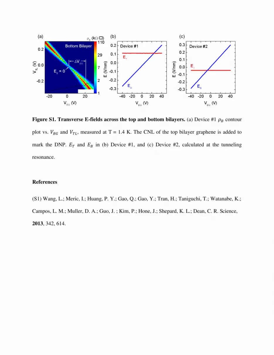
Figure S1. Transverse E-fields across the top and bottom bilayers. (a) Device #1 contour
plot vs. 弔 and 脹, measured at T = 1.4 K. The CNL of the top bilayer graphene is added to
mark the DNP. 脹 and in (b) Device #1, and (c) Device #2, calculated at the tunneling
resonance.
References
(S1) Wang, L.; Meric, I.; Huang, P. Y.; Gao, Q.; Gao, Y.; Tran, H.; Taniguchi, T.; Watanabe, K.;
Campos, L. M.; Muller, D. A.; Guo, J. ; Kim, P.; Hone, J.; Shepard, K. L.; Dean, C. R. Science,
2013, 342, 614.