Embed Size (px)
Citation preview
COMPACT MODELING OF GATE TUNNELING LEAKAGE CURRENT IN ADVANCED NANOSCALE SOI MOSFETS
Ghader Darbandy
Dipòsit Legal: T. 59-2013
ADVERTIMENT. L'accés als continguts d'aquesta tesi doctoral i la seva utilització ha de respectar els drets de la persona autora. Pot ser utilitzada per a consulta o estudi personal, així com en activitats o materials d'investigació i docència en els termes establerts a l'art. 32 del Text Refós de la Llei de Propietat Intel·lectual (RDL 1/1996). Per altres utilitzacions es requereix l'autorització prèvia i expressa de la persona autora. En qualsevol cas, en la utilització dels seus continguts caldrà indicar de forma clara el nom i cognoms de la persona autora i el títol de la tesi doctoral. No s'autoritza la seva reproducció o altres formes d'explotació efectuades amb finalitats de lucre ni la seva comunicació pública des d'un lloc aliè al servei TDX. Tampoc s'autoritza la presentació del seu contingut en una finestra o marc aliè a TDX (framing). Aquesta reserva de drets afecta tant als continguts de la tesi com als seus resums i índexs. ADVERTENCIA. El acceso a los contenidos de esta tesis doctoral y su utilización debe respetar los derechos de la persona autora. Puede ser utilizada para consulta o estudio personal, así como en actividades o materiales de investigación y docencia en los términos establecidos en el art. 32 del Texto Refundido de la Ley de Propiedad Intelectual (RDL 1/1996). Para otros usos se requiere la autorización previa y expresa de la persona autora. En cualquier caso, en la utilización de sus contenidos se deberá indicar de forma clara el nombre y apellidos de la persona autora y el título de la tesis doctoral. No se autoriza su reproducción u otras formas de explotación efectuadas con fines lucrativos ni su comunicación pública desde un sitio ajeno al servicio TDR. Tampoco se autoriza la presentación de su contenido en una ventana o marco ajeno a TDR (framing). Esta reserva de derechos afecta tanto al contenido de la tesis como a sus resúmenes e índices. WARNING. Access to the contents of this doctoral thesis and its use must respect the rights of the author. It can be used for reference or private study, as well as research and learning activities or materials in the terms established by the 32nd article of the Spanish Consolidated Copyright Act (RDL 1/1996). Express and previous authorization of the author is required for any other uses. In any case, when using its content, full name of the author and title of the thesis must be clearly indicated. Reproduction or other forms of for profit use or public communication from outside TDX service is not allowed. Presentation of its content in a window or frame external to TDX (framing) is not authorized either. These rights affect both the content of the thesis and its abstracts and indexes.
UNIVERSITAT ROVIRA I VIRGILI COMPACT MODELING OF GATE TUNNELING LEAKAGE CURRENT IN ADVANCED NANOSCALE SOI MOSFETS Ghader Darbandy Dipòsit Legal: T. 59-2013

UNIVERSITAT ROVIRA I VIRGILI COMPACT MODELING OF GATE TUNNELING LEAKAGE CURRENT IN ADVANCED NANOSCALE SOI MOSFETS Ghader Darbandy Dipòsit Legal: T. 59-2013
Ghader Darbandy
Compact Modeling of Gate Tunneling Leakage Current
in Advanced Nanoscale SOI MOSFETs
Doctoral thesis supervised by Professor Benjamin Iñiguez
Department of Electronic, Electrical and Automatic Control Engineering
Tarragona 2012
UNIVERSITAT ROVIRA I VIRGILI COMPACT MODELING OF GATE TUNNELING LEAKAGE CURRENT IN ADVANCED NANOSCALE SOI MOSFETS Ghader Darbandy Dipòsit Legal: T. 59-2013

UNIVERSITAT ROVIRA I VIRGILI COMPACT MODELING OF GATE TUNNELING LEAKAGE CURRENT IN ADVANCED NANOSCALE SOI MOSFETS Ghader Darbandy Dipòsit Legal: T. 59-2013
i
I STATE that the present study, entitled “Compact Modeling of Gate Tunneling
Leakage Current in Advanced Nanoscale SOI MOSFETs”, presented by Ghader
Darbandy for the award of the degree of the Doctor, has been carried out under my
supervision at the Department of Electrical, Electronic and Automatic Control
Engineering of this university, and that it fulfils all the requirements to be eligible for
the European Doctorate Award.
Doctoral Thesis Supervisor
Prof. Benjamin Iñiguez
Tarragona, October 2012
UNIVERSITAT ROVIRA I VIRGILI COMPACT MODELING OF GATE TUNNELING LEAKAGE CURRENT IN ADVANCED NANOSCALE SOI MOSFETS Ghader Darbandy Dipòsit Legal: T. 59-2013

ii GHADER DARBANDY
UNIVERSITAT ROVIRA I VIRGILI COMPACT MODELING OF GATE TUNNELING LEAKAGE CURRENT IN ADVANCED NANOSCALE SOI MOSFETS Ghader Darbandy Dipòsit Legal: T. 59-2013
iii
Acknowledgements
I would like to express my deepest appreciation to all those who have made this thesis
to be materialized. First of all, I am grateful to my master Prof. Benjamin Iñiguez for
his invaluable and endless advice and support. He directed me to interesting topics of
research and at the same time permitted me to follow my own ideas. He has not only
taught me about compact modeling, but he has also taught how to stay confident, how
to have a positive attitude and ….
I would like to express my greatest appreciation to Prof. Antonio Cerdeira, Prof.
Magali Estrada and Prof. Jamal Deen for their discussions and advices. Prof. Lluis
Marshal, the head of the Department of Electronic, Electric and Automatic
Engineering and all personnel of “the department” are sincerely acknowledged for
their warm and helpful collaborations.
I would also like to thank Dr. Thomas Gneiting for giving me the opportunity for my
six months research stage in his company (AdMOS). My special thanks go to all of my
friendly colleagues at AdMOS Company in Germany.
To all my friends, especially Francois Lime, Muthupandian Cheralathan, Alejandra
Castro Carranza, Mike Schwarz, Thomas Holtij and in particular Maria Mendez Malaga
for the helps (who introduced me to the Spanish language and culture) thanks for your
excellent company and making the enjoyable atmosphere. And Kaveh Yalfani, Zahra
Tabookht, and Sara Hajian, thank you for being close to me and supporting me all this
time.
I would like to thank my friend of life Elham, who started the life journey with me and
gave me the best gift so far, our lovely and sweet son Artin. I deeply appreciate my
family and kind brothers for their support and helping me all the difficult times.
… and many others…
Tarragona, Spain,
October, 2012.
UNIVERSITAT ROVIRA I VIRGILI COMPACT MODELING OF GATE TUNNELING LEAKAGE CURRENT IN ADVANCED NANOSCALE SOI MOSFETS Ghader Darbandy Dipòsit Legal: T. 59-2013

iv GHADER DARBANDY
UNIVERSITAT ROVIRA I VIRGILI COMPACT MODELING OF GATE TUNNELING LEAKAGE CURRENT IN ADVANCED NANOSCALE SOI MOSFETS Ghader Darbandy Dipòsit Legal: T. 59-2013
v
It’s our attitude more than our aptitude
that makes our altitude.
UNIVERSITAT ROVIRA I VIRGILI COMPACT MODELING OF GATE TUNNELING LEAKAGE CURRENT IN ADVANCED NANOSCALE SOI MOSFETS Ghader Darbandy Dipòsit Legal: T. 59-2013

vi GHADER DARBANDY
UNIVERSITAT ROVIRA I VIRGILI COMPACT MODELING OF GATE TUNNELING LEAKAGE CURRENT IN ADVANCED NANOSCALE SOI MOSFETS Ghader Darbandy Dipòsit Legal: T. 59-2013
vii
…to the memory … of my wonderful
parents
UNIVERSITAT ROVIRA I VIRGILI COMPACT MODELING OF GATE TUNNELING LEAKAGE CURRENT IN ADVANCED NANOSCALE SOI MOSFETS Ghader Darbandy Dipòsit Legal: T. 59-2013

viii GHADER DARBANDY
UNIVERSITAT ROVIRA I VIRGILI COMPACT MODELING OF GATE TUNNELING LEAKAGE CURRENT IN ADVANCED NANOSCALE SOI MOSFETS Ghader Darbandy Dipòsit Legal: T. 59-2013
ix
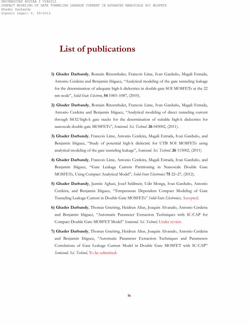
List of publications
1) Ghader Darbandy, Romain Ritzenthaler, Francois Lime, Ivan Garduño, Magali Estrada,
Antonio Cerdeira and Benjamin Iñiguez, “Analytical modeling of the gate tunneling leakage
for the determination of adequate high-k dielectrics in double-gate SOI MOSFETs at the 22
nm node”, Solid-State Electron, 54 1083–1087, (2010).
2) Ghader Darbandy, Romain Ritzenthaler, Francois Lime, Ivan Garduño, Magali Estrada,
Antonio Cerdeira and Benjamin Iñiguez, “Analytical modeling of direct tunneling current
through SiO2/high-k gate stacks for the determination of suitable high-k dielectrics for
nanoscale double-gate MOSFETs”, Semicond. Sci. Technol. 26 045002, (2011).
3) Ghader Darbandy, Francois Lime, Antonio Cerdeira, Magali Estrada, Ivan Garduño, and
Benjamin Iñiguez, “Study of potential high-k dielectric for UTB SOI MOSFETs using
analytical modeling of the gate tunneling leakage”, Semicond. Sci. Technol. 26 115002, (2011)
4) Ghader Darbandy, Francois Lime, Antonio Cerdeira, Magali Estrada, Ivan Garduño, and
Benjamin Iñiguez, “Gate Leakage Current Partitioning in Nanoscale Double Gate
MOSFETs, Using Compact Analytical Model”, Solid-State Electronics 75 22–27, (2012).
5) Ghader Darbandy, Jasmin Aghasi, Josef Seldmeir, Udit Monga, Ivan Garduño, Antonio
Cerdeira, and Benjamin Iñiguez, “Temperature Dependent Compact Modeling of Gate
Tunneling Leakage Current in Double Gate MOSFETs” Solid-State Electronics, Accepted.
6) Ghader Darbandy, Thomas Gneiting, Heidrun Alius, Joaquin Alvarado, Antonio Cerdeira
and Benjamin Iñiguez, “Automatic Parameter Extraction Techniques with IC-CAP for
Compact Double Gate MOSFET Model” Semicond. Sci. Technol, Under review.
7) Ghader Darbandy, Thomas Gneiting, Heidrun Alius, Joaquin Alvarado, Antonio Cerdeira
and Benjamin Iñiguez, “Automatic Parameter Extraction Techniques and Parameters
Correlations of Gate Leakage Current Model in Double Gate MOSFET with IC-CAP”
Semicond. Sci. Technol, To be submitted.
UNIVERSITAT ROVIRA I VIRGILI COMPACT MODELING OF GATE TUNNELING LEAKAGE CURRENT IN ADVANCED NANOSCALE SOI MOSFETS Ghader Darbandy Dipòsit Legal: T. 59-2013

x GHADER DARBANDY
UNIVERSITAT ROVIRA I VIRGILI COMPACT MODELING OF GATE TUNNELING LEAKAGE CURRENT IN ADVANCED NANOSCALE SOI MOSFETS Ghader Darbandy Dipòsit Legal: T. 59-2013
xi
Contents
Introduction 1
Chapter 1: Analytical modeling of the gate tunneling leakage for the determination of
adequate high-k dielectrics in double-gate SOI MOSFETs at the 22 nm node 11
Chapter 2: Analytical Modeling of Direct Tunneling Current through Gate Stacks for
the Determination of Suitable High-k Dielectrics for Double-Gate MOSFETs 25
Chapter 3: Study of Potential High-k Dielectric for UTB SOI MOSFETs Using
Analytical Modeling of the Gate Tunneling Leakage 45
Chapter 4: Gate Leakage Current Partitioning in Nanoscale Double Gate MOSFETs,
Using Compact Analytical Model 67
Chapter 5: Temperature Dependent Compact Modeling of Gate Tunneling Leakage
Current in Double Gate MOSFETs 85
Chapter 6: An Automatic Parameter Extraction Procedure for an Explicit Surface
Potential Based Compact Double Gate MOSFET Model 101
Chapter 7: Automatic Parameter Extraction Techniques and Parameters Correlations
of Gate Leakage Current Model in Double Gate MOSFET with IC-CAP 117
General Conclusions 131
UNIVERSITAT ROVIRA I VIRGILI COMPACT MODELING OF GATE TUNNELING LEAKAGE CURRENT IN ADVANCED NANOSCALE SOI MOSFETS Ghader Darbandy Dipòsit Legal: T. 59-2013

xii GHADER DARBANDY
UNIVERSITAT ROVIRA I VIRGILI COMPACT MODELING OF GATE TUNNELING LEAKAGE CURRENT IN ADVANCED NANOSCALE SOI MOSFETS Ghader Darbandy Dipòsit Legal: T. 59-2013
1
Introduction
Transistor is the fundamental building block of modern electronic devices. It is a
semiconductor device used to amplify and switch electronic signals and electrical
power. The transistor is the key active component in practically all modern electronics.
Many consider it to be one of the greatest inventions of the 20th century [1].
The first Silicon transistor was produced by Gordon Teal at Texas Instruments in
1954 [2, 3]. The first Metal Oxide Semiconductor (MOS) transistor actually built was
by Kahng and Atalla at Bell Labs in 1960 [4]. Transistors are now part of almost every
person’s daily life. These devices with a majority of cell phones, laptops, iPods, players
and desktop computers have become popular. Users are using such devices for a
variety of functions, including internet, email, music, games and video.
UNIVERSITAT ROVIRA I VIRGILI COMPACT MODELING OF GATE TUNNELING LEAKAGE CURRENT IN ADVANCED NANOSCALE SOI MOSFETS Ghader Darbandy Dipòsit Legal: T. 59-2013
2 GHADER DARBANDY
1) Transistor Scaling and its Challenges
One of the main challenges in the MOS transistor is the reduction of device
dimension. The main concern is to predict the device performance and how the
transistors work and behave as the size of device shrinks down.
“Scaling” refers to reduction of the lateral geometric dimensions of MOSFET
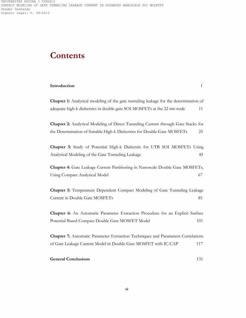
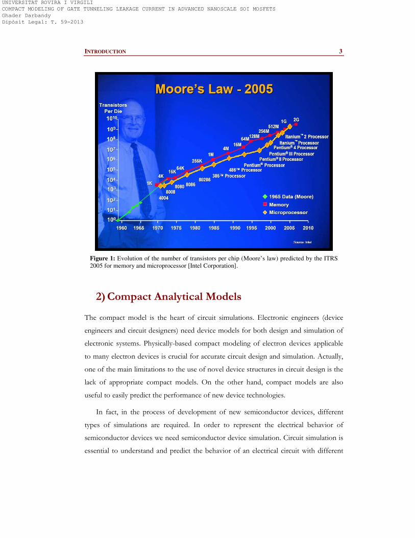
devices. In 1965, Gordon Moore (later a founder of Intel Corporation) published his
famous observation regarding to the evolution of the transistor density in Integrated
Circuits (IC) exponentially over time. “Moore's law” says that the number of
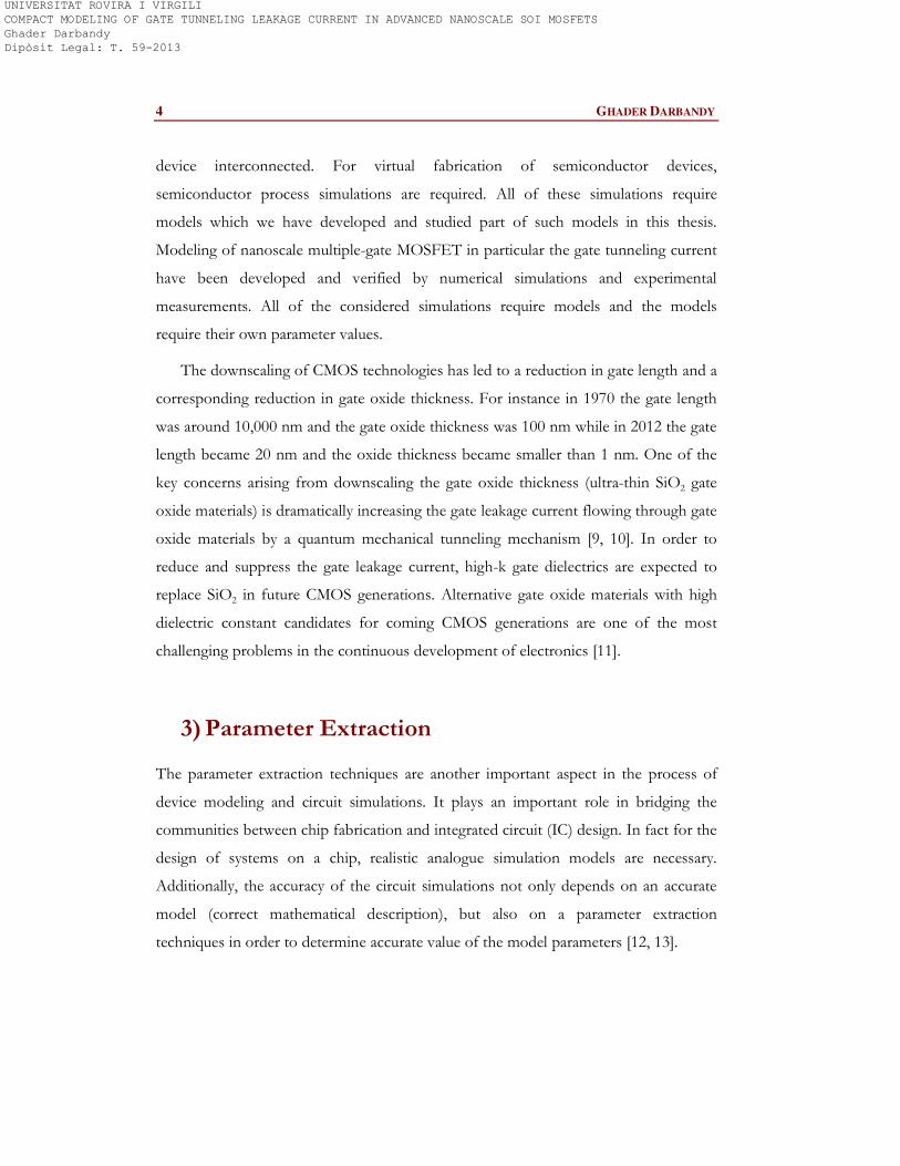
transistors on a chip wills approximately double every 18 months [5]. This prediction
has been the case for many years and remarkably followed by the semiconductor
industry for the last forty years (Figure 1). But even in this early work, there was
question of how long this scaling trend could continue [6].
Only the rate of increase in transistor density has been described by Moore’s Law,
while the reduction of the physical MOS device dimensions has improved both circuit
speed and enabled cheaper ICs. In fact, scaling allows for the manufacturing of more
devices for the same price [7].
Since the early 1990's semiconductor companies and academia decided to predict
the future of semiconductor device industry more precisely. This initiative gave birth to
the International Technology Roadmap for Semiconductor (ITRS) organization [8].
The ITRS issues a report every year that serves as a bench mark for the semiconductor
industry. The reports represent the best opinion on the directions of research into the
type of technology, design tools, equipment and metrology tools that have to be
developed in order to keep pace with the exponential progress of semiconductor
devices predicted by Moore’s law, including time-lines up to about 15 years into the
future [6]. Figure 1 shows the evolution of the transistors per chip (Moore’s law)
predicted by the ITRS 2005 for memory and microprocessor.
UNIVERSITAT ROVIRA I VIRGILI COMPACT MODELING OF GATE TUNNELING LEAKAGE CURRENT IN ADVANCED NANOSCALE SOI MOSFETS Ghader Darbandy Dipòsit Legal: T. 59-2013
INTRODUCTION 3
Figure 1: Evolution of the number of transistors per chip (Moore’s law) predicted by the ITRS
2005 for memory and microprocessor [Intel Corporation].
2) Compact Analytical Models
The compact model is the heart of circuit simulations. Electronic engineers (device
engineers and circuit designers) need device models for both design and simulation of
electronic systems. Physically-based compact modeling of electron devices applicable
to many electron devices is crucial for accurate circuit design and simulation. Actually,
one of the main limitations to the use of novel device structures in circuit design is the
lack of appropriate compact models. On the other hand, compact models are also
useful to easily predict the performance of new device technologies.
In fact, in the process of development of new semiconductor devices, different
types of simulations are required. In order to represent the electrical behavior of
semiconductor devices we need semiconductor device simulation. Circuit simulation is
essential to understand and predict the behavior of an electrical circuit with different
UNIVERSITAT ROVIRA I VIRGILI COMPACT MODELING OF GATE TUNNELING LEAKAGE CURRENT IN ADVANCED NANOSCALE SOI MOSFETS Ghader Darbandy Dipòsit Legal: T. 59-2013
4 GHADER DARBANDY
device interconnected. For virtual fabrication of semiconductor devices,
semiconductor process simulations are required. All of these simulations require
models which we have developed and studied part of such models in this thesis.
Modeling of nanoscale multiple-gate MOSFET in particular the gate tunneling current
have been developed and verified by numerical simulations and experimental
measurements. All of the considered simulations require models and the models
require their own parameter values.
The downscaling of CMOS technologies has led to a reduction in gate length and a
corresponding reduction in gate oxide thickness. For instance in 1970 the gate length
was around 10,000 nm and the gate oxide thickness was 100 nm while in 2012 the gate
length became 20 nm and the oxide thickness became smaller than 1 nm. One of the
key concerns arising from downscaling the gate oxide thickness (ultra-thin SiO2 gate
oxide materials) is dramatically increasing the gate leakage current flowing through gate
oxide materials by a quantum mechanical tunneling mechanism [9, 10]. In order to
reduce and suppress the gate leakage current, high-k gate dielectrics are expected to
replace SiO2 in future CMOS generations. Alternative gate oxide materials with high
dielectric constant candidates for coming CMOS generations are one of the most
challenging problems in the continuous development of electronics [11].
3) Parameter Extraction
The parameter extraction techniques are another important aspect in the process of
device modeling and circuit simulations. It plays an important role in bridging the
communities between chip fabrication and integrated circuit (IC) design. In fact for the
design of systems on a chip, realistic analogue simulation models are necessary.
Additionally, the accuracy of the circuit simulations not only depends on an accurate
model (correct mathematical description), but also on a parameter extraction
techniques in order to determine accurate value of the model parameters [12, 13].
UNIVERSITAT ROVIRA I VIRGILI COMPACT MODELING OF GATE TUNNELING LEAKAGE CURRENT IN ADVANCED NANOSCALE SOI MOSFETS Ghader Darbandy Dipòsit Legal: T. 59-2013
INTRODUCTION 5
The commercial package (IC-CAP) is used to apply automatic parameter extraction
techniques and simulating our models which is coded in Verilog-A. The Verilog-A
language is a source code of the compact model and one of the best tools for compact
modeling which is actually compatible with IC-CAP (program of Agilent). Automatic
parameter extraction routines provide an effective way to calculate the model
parameters to minimize discrepancies between measured and model calculations.
4) Thesis Organization
This thesis is aimed to present the novel high-k dielectric materials that can work as
gate oxides in Double Gate (DG) device structures for the 22 nm low standby power
applications. A guideline for the determination of the suitable high-k candidate is
reported in the case of ideal interface (one layer gate oxide material) and in the case of
a SiO2/high-k gate stack in a nanoscale single gate and DG MOSFETs. The effect of
interfacial layer thickness is studied in order to select the most promising high-k
candidates for different values of the Equivalent Oxide Thickness (EOT) and SiO2
interfacial layer thicknesses.
A compact gate leakage current partitioning model is presented for nanoscale DG
MOSFETs, using analytical models of the direct tunneling gate leakage current.
Temperature dependent analytical models of the direct tunneling gate leakage current
in inversion region and the Trap Assisted Tunneling (TAT) current in subthreshold
regime have been developed for DG FinFET with a two dielectric layers gate stack
such as SiON/SiO2. As the last part, we studied the parameter extraction relies on a
commercial software package (IC-CAP) allowing automatic parameter extraction
routines and provides an effective way to calculate the model parameters to minimize
discrepancies between measured and modeled data for reliable circuit simulation.
Additionally, each chapter of this thesis is subjected to the following objectives:
Chapter 1: Analytical modeling of the gate tunneling leakage for the determination of
adequate high-k dielectrics in double-gate SOI MOSFETs at the 22 nm node. A
UNIVERSITAT ROVIRA I VIRGILI COMPACT MODELING OF GATE TUNNELING LEAKAGE CURRENT IN ADVANCED NANOSCALE SOI MOSFETS Ghader Darbandy Dipòsit Legal: T. 59-2013
6 GHADER DARBANDY
theoretical study to the ideal interface between high-k material and Si substrate without
any interfacial layer is presented [14].
Chapter 2: Analytical modeling of the direct tunneling current through gate stacks for
the determination of suitable high-k dielectrics for nanoscale double-gate MOSFETs.
A guideline for the determination of the suitable high-k candidate was reported in the
case of a SiO2/high-k gate stack in a nanoscale DG MOSFET. The models
demonstrate that the materials such as La2O3, HfO2, LaAlO3 and Pr2O3 in the
hexagonal phase would fulfill the considered requirements [15].
Chapter 3: Study of potential high-k dielectric for UTB SOI MOSFETs using
analytical modeling of the gate tunneling leakage. The most important criteria for
selecting alternative dielectrics (maximum gate leakage current, EOT, electron effective
mass, dielectric constant k-value, barrier height and SiO2 thickness as an interfacial
layer) were taken into account to determine the suitability of the gate oxide materials
[16].
Chapter 4: Gate leakage current partitioning in nanoscale DG MOSFETs, using
compact analytical model. A model of the partitioning of the gate to channel tunneling
leakage current into the source and drain components is developed. The influence and
impact of the thickness of the interfacial SiO2 layer on the gate-drain and gate-source
components has been shown [17].
Chapter 5: Temperature dependent compact analytical modeling of gate tunneling
leakage current in DG MOSFETs is studied. The gate leakage current measurements at
different temperatures show two different transport mechanisms, DT gate leakage
current in the strong inversion regime and TAT current in the sub-threshold regime
[18].
Chapter 6: Automatic parameter extraction techniques in IC-CAP for compact DG
MOSFET model are studied. We have developed automatic parameter extraction
techniques for our explicit compact model in DG MOSFET suitable for design and
circuits simulation based on surface potential including short channel effects [19].
UNIVERSITAT ROVIRA I VIRGILI COMPACT MODELING OF GATE TUNNELING LEAKAGE CURRENT IN ADVANCED NANOSCALE SOI MOSFETS Ghader Darbandy Dipòsit Legal: T. 59-2013
INTRODUCTION 7
Chapter 7: Automatic Direct Tunneling and TAT Gate Leakage Current Parameter
Extraction Techniques and Parameters Correlations in Double Gate MOSFET. The
commercial package IC-CAP is used to simulate our leakage current model coded in
Verilog-A, and comparing with gate leakage measurements in order to obtain
parameters and study parameters correlations [20].
References
[1] Robert W. Price (2004). Roadmap to Entrepreneurial Success, AMACOM Div American
Mgmt Assn. p. 42, ISBN 978-0-8144-7190-6
[2] J. Chelikowski, "Introduction: Silicon in all its Forms", Silicon: evolution and future of a
technology (Editors: P. Siffert, E. F. Krimmel), p.1, Springer, 2004 ISBN 3-540-40546-1
[3] W. Heywang, K. H. Zaininger, "Silicon: The Semiconductor Material", Silicon:
evolution and future of a technology (Editors: P. Siffert, E. F. Krimmel), p.36, Springer, 2004
ISBN 3-540-40546-1
[4] W. Heywang, K. H. Zaininger, "Silicon: The Semiconductor Material", Silicon:
evolution and future of a technology (Editors: P. Siffert, E. F. Krimmel), p.36, Springer, 2004
ISBN 3-540-40546-1
[5] G. E. Moore, Cramming more components onto integrated circuits. Electronics,
Vol. 38, pp. 114 -117 (1965)
[6] J.-P. Colinge, FinFETs and Other Multi-Gate Transistors, NewYork, Springer-
Verlag, 2008.
[7] J. M. Rabaey, A. Chandrakasan, and B. Nikolić, Digital Integrated Circuits: A
Design Perpsective, Upper Saddle River: Prentice Education, Inc., pp. 122-128, 2003.
[8] International Technology Roadmap for Semiconductors, ITRS. [Online] 2012,
http://www.itrs.net/
UNIVERSITAT ROVIRA I VIRGILI COMPACT MODELING OF GATE TUNNELING LEAKAGE CURRENT IN ADVANCED NANOSCALE SOI MOSFETS Ghader Darbandy Dipòsit Legal: T. 59-2013
8 GHADER DARBANDY
[9] Depas M, Vermeire B, Mertens P W, Van Meirhaeghe R L and Heyns M M 1995
Determination of tunneling parameters in ultra-thin oxide layer poly-Si/SiO2/Si
structures Solid-State Electron, 38 1465
[10] Lo S H, Buchanan D A, Taur Y and Wang W 1997 Quantum-mechanical
modeling of electron tunneling current from the inversion layer of ultra-thin-oxide
nMOSFET’s IEEE Electron Device Lett. 18 209
[11] Iwai H and Ohmi S 2002 Silicon integrated circuit technology from past to future
Microelectron. Reliab. 42 465–91
[12] N. Chevillon, M. Tang, F. Pregaldiny, C. Lallement and M. Madec, "FinFET
Compact Modelling and parameter extraction", Proc. 16th Int. Conf. Mixed Design of
Integrated Circuits and Systems (MIXDES'09)
[13] Joaquın Alvarado1, Benjamin Iniguez, Magali Estrada, Denis Flandre and Antonio
Cerdeira, “Implementation of the symmetric doped double-gate MOSFET model in
Verilog-A for circuit simulation”, Int. J. Numer. Model, 2010; 23:88–106.
[14] Darbandy G, Ritzenthaler R, Lime F, Garduno I, Estrada M, Cerdeira A and I˜
niguez B 2010 Analytical modeling of the gate tunneling leakage for the determination
of adequate high-k dielectrics in double-gate SOI MOSFETs at the 22 nm node. Solid-
State Electron, 54 1083–7
[15] Darbandy G, Ritzenthaler R, Lime F, Garduno I, Estrada M, Cerdeira A and
Iniguez B 2011 Analytical modeling of direct tunneling current through SiO2/high-k
gate stacks for the determination of suitable high-k dielectrics for nanoscale double-
gate MOSFETs, Semicond. Sci. Technol. 26 045002
[16] Darbandy G, Lime F, Cerdeira A, Estrada M, Garduno I, and Iniguez B 2011
Study of potential high-k dielectric for UTB SOI MOSFETs using analytical modeling
of the gate tunneling leakage, Semicond. Sci. Technol. 26 (2011) 115002
[17] Ghader Darbandy, Francois Lime, Antonio Cerdeira, Magali Estrada, Ivan
Garduño, and Benjamin Iñiguez, “Gate Leakage Current Partitioning in Nanoscale
UNIVERSITAT ROVIRA I VIRGILI COMPACT MODELING OF GATE TUNNELING LEAKAGE CURRENT IN ADVANCED NANOSCALE SOI MOSFETS Ghader Darbandy Dipòsit Legal: T. 59-2013
INTRODUCTION 9
Double Gate MOSFETs, Using Compact Analytical Model”, Solid-State Electronics 75
(2012) 22–27.
[18] Ghader Darbandy, Jasmin Aghasi, Josef Seldmeir, Udit Monga, Ivan Garduño,
Antonio Cerdeira, and Benjamin Iñiguez, “Compact Analytical Modeling for
Temperature Dependent of Gate Tunneling Leakage Current in Double Gate
MOSFETs” Solid-State Electronics, Accepted.
[19] Ghader Darbandy, Thomas Gneiting, Heidrun Alius, Joaquin Alvarado, Antonio
Cerdeira and Benjamin Iñiguez, “Automatic Parameter Extraction Techniques with IC-
CAP for Compact Double Gate MOSFET Model”, Semicond. Sci. Technol. Under
Review.
[20] Ghader Darbandy, Thomas Gneiting, Heidrun Alius, Joaquin Alvarado, Antonio
Cerdeira and Benjamin Iñiguez, “Automatic Parameter Extraction Techniques and
Parameters Correlations of Gate Leakage Current Model in Double Gate MOSFET
with IC-CAP” Semicond. Sci. Technol, To be submitted
UNIVERSITAT ROVIRA I VIRGILI COMPACT MODELING OF GATE TUNNELING LEAKAGE CURRENT IN ADVANCED NANOSCALE SOI MOSFETS Ghader Darbandy Dipòsit Legal: T. 59-2013

10 GHADER DARBANDY
UNIVERSITAT ROVIRA I VIRGILI COMPACT MODELING OF GATE TUNNELING LEAKAGE CURRENT IN ADVANCED NANOSCALE SOI MOSFETS Ghader Darbandy Dipòsit Legal: T. 59-2013
11
Chapter 1
Analytical Modeling of Gate Tunneling Leakage for the
Determination of Adequate High-k Dielectrics in
Double-Gate SOI MOSFETs at the 22 nm node
The gate leakage current in metal-oxide-semiconductor (MOS) junctions/devices/or
transistors is modeled and studied in order to find promising materials for double gate
(DG) MOSFETs at 22 nm node by considering analytical models of the direct
tunneling current (based on a proper calculation of the WKB tunneling probability in
the gate oxide). We present a theoretical study to find the most promising gate oxide
materials for the 22 nm technological node with the predicted maximum value of
leakage current (10-2 [A/cm2]) that is tolerable for that node, according to the ITRS
roadmap. The effects of electron effective mass, dielectric constant k value and barrier
height on the cE∆ -k permitted values have been studied.
UNIVERSITAT ROVIRA I VIRGILI COMPACT MODELING OF GATE TUNNELING LEAKAGE CURRENT IN ADVANCED NANOSCALE SOI MOSFETS Ghader Darbandy Dipòsit Legal: T. 59-2013
12 GHADER DARBANDY
1) Introduction
Aggressive scaling of CMOS technology in recent years has reduced the silicon dioxide
gate dielectric thickness below 2 nm. Finding an alternative gate material with high
dielectric constants for coming CMOS generations is one of the most challenging
problems in the continuous development of microelectronics [1]. In order to reduce
the gate leakage current, high-k gate dielectrics are expected to replace SiO2 in future
CMOS generations. Introducing a physically thicker high-k material can reduce the
leakage current to the acceptable limit. Keeping at the same time a high enough value
of the drain current in On-state (because of the higher dielectric constant).
Two of the most elementary quantities that need to be considered are the dielectric
constant k and the energy band-offset values cE∆ between the conduction band of the
oxide materials and the silicon substrate [2]. It is not straightforward to replace SiO2
with an alternative gate dielectric. The required properties of gate dielectrics should be
systematically considered to provide the key guidelines for selecting an alternative gate
dielectric.
The k of candidate oxides tends to vary inversely with the band gap, so we must
accept a not too high-k value [3]. There are of course oxides with extremely large k
values, such as ferroelectrics like BaTiO3 but these have too low band gap. In fact, a
huge k is undesirable in CMOS design because they cause undesirably strong fringing
fields at source and drain electrodes [4]. Since the key motivation for replacing SiO2
with high-k materials is leakage reduction, accurate modeling of the leakage current is
necessary to understand the scaling limits and ensure that the selected materials are
highly scalable and usable for many future generations of technology. In this work, we
suppose that direct tunneling is the dominant conduction mechanism.
Due to the excellent control of short channel effects, Double-Gate (DG)
MOSFET has emerged as one of the most promising devices for circuit design in sub-
32 nm regime. However as explained before, the gate direct tunneling current is
becoming a major source of leakage with aggressive scaling of oxide thickness [5, 6].
Therefore, it is necessary to analyze the gate leakage in sub-32 nm DG MOS devices.
UNIVERSITAT ROVIRA I VIRGILI COMPACT MODELING OF GATE TUNNELING LEAKAGE CURRENT IN ADVANCED NANOSCALE SOI MOSFETS Ghader Darbandy Dipòsit Legal: T. 59-2013
CHAPTER 1 13
The better gate control reduces the vertical electric field, and as a consequence, the
gate leakage in a DG MOSFET is lower than in its bulk-CMOS counterpart at the
same bias conditions [7]. In [8] an expression of the direct-tunneling current density
for an oxide voltage drop smaller than the barrier height is given.
The tunneling electron effective mass mox increases while decreasing the oxide
thickness Tox and mox for Vox >1.5 V is about a factor of 0.8 times smaller than mox for
Vox<1.5 V. It was reported that the apparent increase of the conduction band effective
mass in ultra thin SiO2 with decreasing Tox is consistent with a narrowing of the energy
bands due to the decreased dimensionality [9].
Accurate simple and improved models for the direct tunneling current through
high-k gate dielectrics adapted to DG MOSFETs are presented. We present a
theoretical study to the ideal interface between high-k material and Si substrate without
any interfacial layer, using these models, three of the most fundamental quantities that
are needed: the dielectric constant (k), the energy band-offset values ( cE∆ ) between
the conduction band of the oxide and the silicon substrate, and electron effective mass
to determine promising gate oxide materials for further DG MOSFETs technologies
[10]. Our goal is to make the study of the best possible case (ideal device without
interfacial layer).
2) Simple Analytical Model
In the case of the 22 nm node, for low standby power operation, an oxide EOT of
about 0.5nm is required with a leakage target at 1 V of about 10-2 [A/cm2] [11, 12]. A
simplified estimate of the corresponding requirements for k and cE∆ can be done by
assuming that the most severe leakage mechanism for this case is direct tunneling from
the silicon conduction band to the conduction band of the dielectric.
Our analysis applies to the ideal case of direct tunneling in high-k dielectric films
and ideal interface without trap assisted tunneling [13], which may be present at low
electric fields (low gate voltage) in these dielectrics (especially if the quality of the
UNIVERSITAT ROVIRA I VIRGILI COMPACT MODELING OF GATE TUNNELING LEAKAGE CURRENT IN ADVANCED NANOSCALE SOI MOSFETS Ghader Darbandy Dipòsit Legal: T. 59-2013
14 GHADER DARBANDY
interface is not very good [14]). Additionally, we have made our analysis at Vg=1V
which is well above the threshold voltage and therefore Direct Tunneling is clearly
dominant over TAT [15, 16].
We have adapted to the DG MOSFET structure a relatively simple analytical
model for the gate direct tunneling leakage (assumed to be the main gate leakage
component) [12, 17], incorporating it to our previous compact model for the potential
and drain current of a DG MOSFET [18, 19]. The direct-tunneling current density for
an oxide voltage smaller than the barrier height can be simply expressed as:
}
])1(1.[
exp{)12
()(
2
3
2
ox
C
ox
ox
ox
C
ox
Cn
E
E
VB
EV
E
V
EAJ
∆−−−
××−∆
×∆
×= (1)
where; CEh
qA
∆=
π8
3
,hq
EmB
Cox
3
28 2
3
∆=
πand Eox=Vox/Tox
where cE∆ is the conduction band offset for a dielectric material, q is the electron
charge, Tox is the oxide thickness, h is the Planck constant, mox correspond to the
electron tunneling effective mass in the dielectric layer, and Vox is the voltage across the
material which for the tunneling it was suggested [8, 20].
The voltage across the gate dielectric layer Vox is given by the relation:
Vox = Vg – VFB – ψs (2)
where Vg is the applied gate voltage, VFB is flat band voltage; ψs is the band bending at
the interface (surface potential). This surface potential is obtained using our previous
compact model for the potential of a DG MOSFET [18, 19].
The functions cE∆ = f(kh) as given by Eq. (1) are plotted for the different cases
together with the data points in the figures and considered as borders for estimating
the relations between band offset values and dielectric constants for the low standby
power requirements of the 22 nm node.
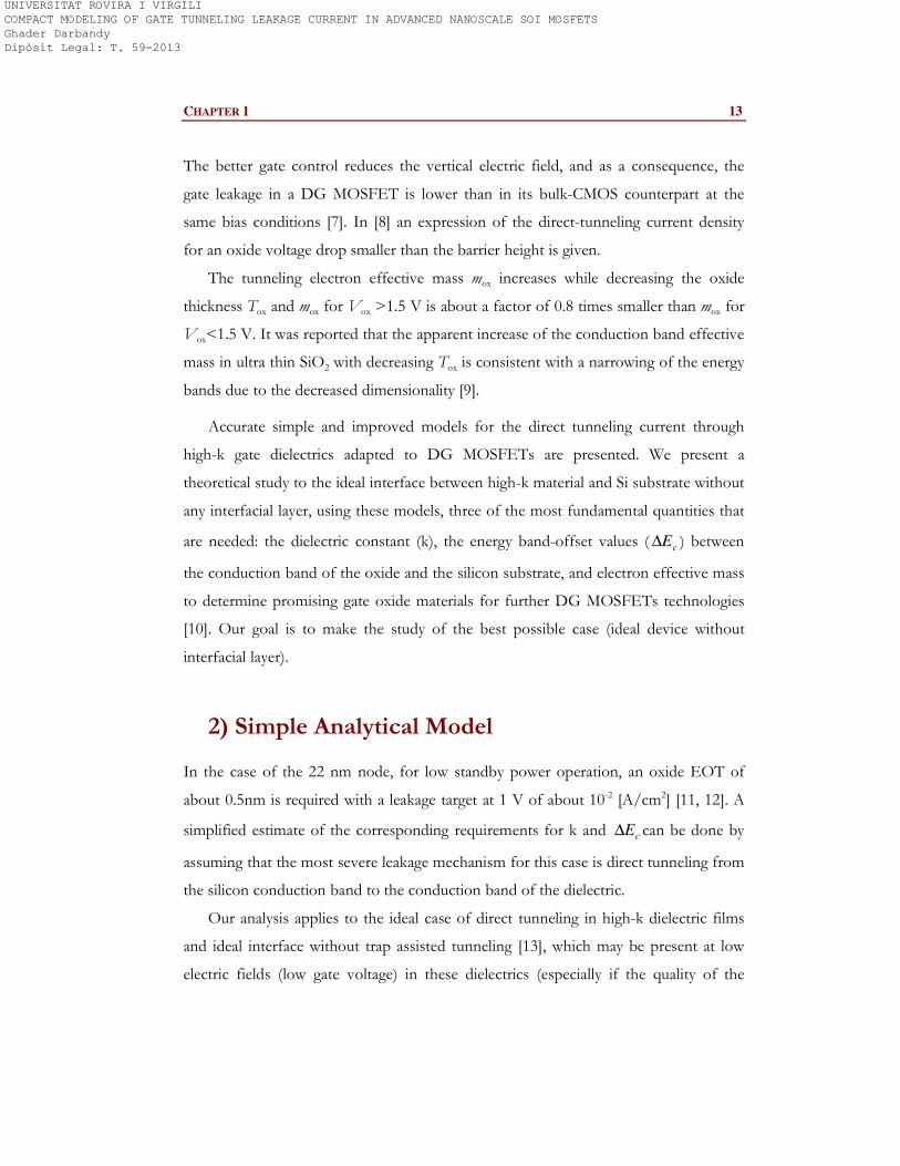
Results with our model suggest alternative dielectric materials such as Ce2O3 and
LaAlO3 in the most aggressive gate dielectric scaling scenario for low standby power
UNIVERSITAT ROVIRA I VIRGILI COMPACT MODELING OF GATE TUNNELING LEAKAGE CURRENT IN ADVANCED NANOSCALE SOI MOSFETS Ghader Darbandy Dipòsit Legal: T. 59-2013
CHAPTER 1 15
La2O3
Ce2O3CeO2
Pr2O3(Amor)Pr2O3(Hex)
Sm2O3
Gd2O3
Ho2O3
Er2O3
Yb2O3
Lu2O3
HfO2
Y2O3
ZrO2
LaAlO3
La2CuO4
LiNbO3
LaScO3
ScO3
0
0,5
1
1,5
2
2,5
3
3,5
4
4,5
0 10 20 30 40 50 60
Dielectric Constant K[1]
Ba
nd
Off
se
t ∆
EC
[e
V]
m*=0.26m0 Simple model
Selected materials
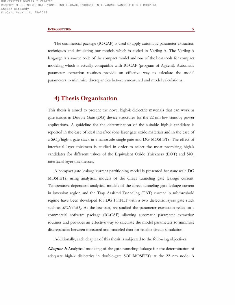
Figure 1: Band offset between conduction bands for different oxides and silicon as a function of
k-value, for an oxide EOT of 0.5nm, m*=0.26m0, Vg=1V with a leakage current about 10
-2
[A/cm2], using the simple analytical model.
technology requirements. It has been demonstrated that, for EOT=0.5nm and
m*=0.26m0 [10], Ce2O3, and LaAlO3 in Figure1 give a leakage current of about 10-2
[A/cm2] at 1 V with a transport mechanism assumed to be direct tunneling as the most
important component from simple model. Ce2O3 and LaAlO3 have particularly large
potential barrier offsets which mean that they could be the next generation high-k
oxides with the required leakage currents.
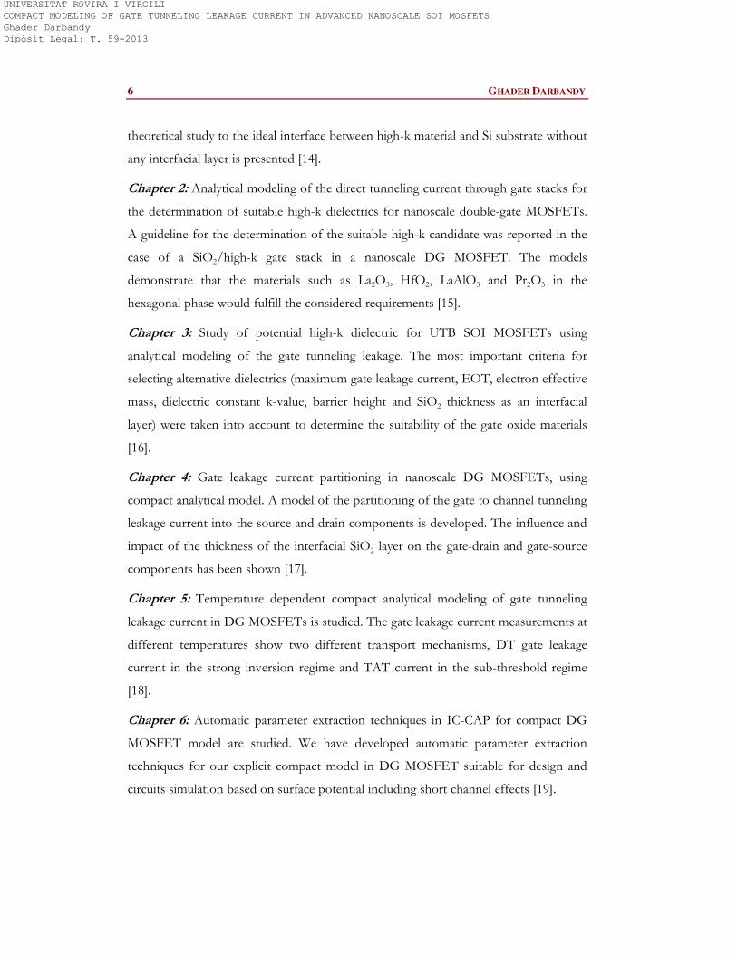
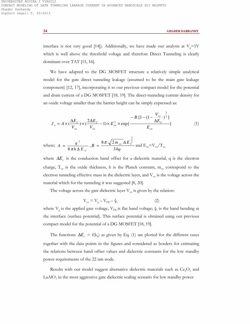
Figure 2 shows the results for the minimum (m*=0.20m0) and maximum value
(m*=0.50m0) of the electron effective mass for various dielectric materials taken from
the literature [11, 21, 22]. It is remarkable that there is a strong dependence on the
electron effective mass that is used and that it should be taken into account when
evaluating new dielectric materials as a gate oxide. Therefore, it is necessary to
accurately know the value of the electron effective mass in any new gate dielectric.
UNIVERSITAT ROVIRA I VIRGILI COMPACT MODELING OF GATE TUNNELING LEAKAGE CURRENT IN ADVANCED NANOSCALE SOI MOSFETS Ghader Darbandy Dipòsit Legal: T. 59-2013
16 GHADER DARBANDY
La2O3Ce2O3
CeO2
Pr2O3(Amor)
Pr2O3(Hex)
Sm2O3
Gd2O3
Ho2O3
Er2O3
Yb2O3
Lu2O3
HfO2
Y2O3
ZrO2
LaAlO3
La2CuO4
LiNbO3
LaScO3
ScO3
0
0,5
1
1,5
2
2,5
3
3,5
4
4,5
0 10 20 30 40 50 60
Dielectric Constant K[1]
Ban
d O
ffs
et ∆
EC
[eV
]
m*=0.50m0, m*=0.20m0 Simple model
Selected materials
Figure 2: Band offset between conduction bands for different oxides and silicon as a function of
k-value, for an oxide EOT of 0.5nm, Vg=1V, J=10-2 [A/cm2], with effective mass m*=0.20m0
and m*=0.50m0, using the simple analytical model.
For EOT=0.5nm, Pr2O3 in the hexagonal phase as well as La2O3 and LaAlO3 are
suitable dielectrics which give the required leakage current with m*=0.20m0. When
changing the effective mass to m*=0.50m0, the suitable materials then change to CeO2,
and Pr2O3 in the amorphous phase (see Figure 2).
Additionally Figure 2 shows the effect of changing the value of the electron
effective mass in a range from m*=0.20m0 to m*=0.50m0, because this parameter
almost changes in wide range [22]. The materials such as Ce2O3, LaScO3, DyScO3,
GdScO3, ZrO2, and HfO2 could be possible from the point of view of the barrier
height, dielectric constant-k, and electron effective mass for EOT=0.5nm, Vg=1V, and
leakage current J=0.01 [A/cm2].
UNIVERSITAT ROVIRA I VIRGILI COMPACT MODELING OF GATE TUNNELING LEAKAGE CURRENT IN ADVANCED NANOSCALE SOI MOSFETS Ghader Darbandy Dipòsit Legal: T. 59-2013
CHAPTER 1 17
Ce2O3
CeO2
Pr2O3(Amor) Pr2O3(Hex)
Ho2O3
Yb2O3
Lu2O3
Y2O3
ZrO2 LaAlO3
La2CuO4
LiNbO3
LaScO3
ScO3
SiO2
Al2O3
HfO2
La2O3
LaLuO3
0
0.5
1
1.5
2
2.5
3
3.5
4
4.5
0 10 20 30 40 50 60 70
Dielectric Constant K[1]
Ba
nd
Off
se
t ∆
EC
[e
V]
EOT=0.8nm, EOT=0.5nm, EOT=0.3nm Simple model
Selected materials
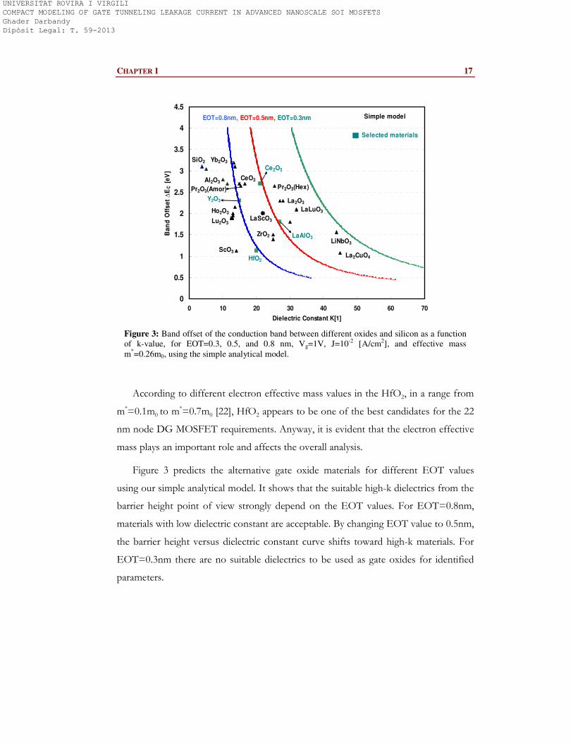
Figure 3: Band offset of the conduction band between different oxides and silicon as a function
of k-value, for EOT=0.3, 0.5, and 0.8 nm, Vg=1V, J=10-2 [A/cm2], and effective mass
m*=0.26m0, using the simple analytical model.
According to different electron effective mass values in the HfO2, in a range from
m*=0.1m0 to m*=0.7m0 [22], HfO2 appears to be one of the best candidates for the 22
nm node DG MOSFET requirements. Anyway, it is evident that the electron effective
mass plays an important role and affects the overall analysis.
Figure 3 predicts the alternative gate oxide materials for different EOT values
using our simple analytical model. It shows that the suitable high-k dielectrics from the
barrier height point of view strongly depend on the EOT values. For EOT=0.8nm,
materials with low dielectric constant are acceptable. By changing EOT value to 0.5nm,
the barrier height versus dielectric constant curve shifts toward high-k materials. For
EOT=0.3nm there are no suitable dielectrics to be used as gate oxides for identified
parameters.
UNIVERSITAT ROVIRA I VIRGILI COMPACT MODELING OF GATE TUNNELING LEAKAGE CURRENT IN ADVANCED NANOSCALE SOI MOSFETS Ghader Darbandy Dipòsit Legal: T. 59-2013
18 GHADER DARBANDY
3) Improved Analytical Model
The simple model expression includes a number of approximations that can lead to
inaccuracies. The finite density of electrons or energy states in the semiconductor
needs to be accounted for. The assumption of a constant effective mass for all energies
(all locations at any oxide thickness and gate bias) is not accurate either. Furthermore,
as oxide becomes thinner, the quantization effects in the semiconductor have to be
considered in order to obtain the oxide potentials as an accurate function of the gate
voltage [23, 24].
Because of these reasons, the simple analytical model falls short of a complete
description of the tunneling current and is unable to fit the tunneling current for the
entire range. A correction function is needed in order to cover the second-order effects
listed above.
We used for the DG MOSFET structure a more complex and accurate analytical
model for the direct tunneling gate current [25] that was adapted to the DG MOSFET
[26] and presented in [18, 19]. The current density due to direct tunneling is expressed
as follows
]})1(1[.
exp{.. 2
3
C
ox
ox
ph
i
nE
V
V
tBEC
AJ
∆−−−=
ε (3)
where iε is the gate dielectric constant, Vox is the voltage drop across the gate
dielectric, cE∆ as previously said is the conduction band offset for a dielectric material
and tph is the physical dielectric thickness as:
EOTk
kt
SiO
kHigh
ph ×=−
)(
2
UNIVERSITAT ROVIRA I VIRGILI COMPACT MODELING OF GATE TUNNELING LEAKAGE CURRENT IN ADVANCED NANOSCALE SOI MOSFETS Ghader Darbandy Dipòsit Legal: T. 59-2013
CHAPTER 1 19
La2O3
Ce2O3CeO2
Pr2O3(Amor)Pr2O3(Hex)
Sm2O3
Gd2O3
Ho2O3
Er2O3
Yb2O3
Lu2O3
HfO2
Y2O3
ZrO2
LaAlO3
La2CuO4
LiNbO3
LaScO3
ScO3
0
0,5
1
1,5
2
2,5
3
3,5
4
4,5
0 10 20 30 40 50 60
Dielectric Constant K[1]
Ban
d O
ffset ∆
EC [
eV
]
m*=0.26m0Improved model, αECB=0.6
Selected materials
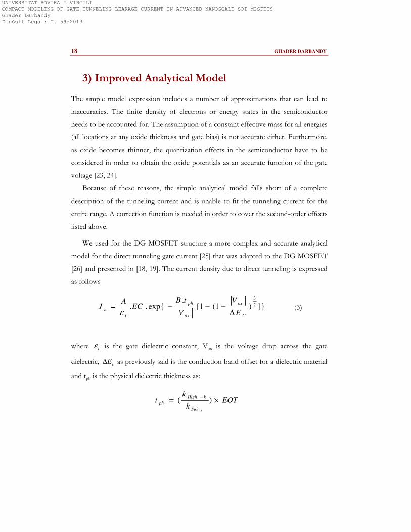
Figure 4: Band offset of the conduction band between different oxides and silicon as a function
of k-value, for an oxide EOT of 0.5nm, m*=0.26m0, Vg=1V, αECB=0.6 with a leakage current 10
-2
[A/cm2], using the improved analytical model.
Factors A and B is expressed as:
CEh
qA
∆=
π8
3
, and hq
EmB
Cox
3
28 2
3
∆=
π
Expression (3) includes the empirical correction function EC described by
)}1()1(20
exp{0 C
oxCox
C
T
ph
GG
E
VEV
EN
t
VVEC ECB
∆−×+
∆−
∆××
∆±= α
φ (4)
Where VG is the applied gate voltage, GV∆ is a fitting parameter to adjust the
origin of the I-V characteristic to coincide with the modeled and the experimental
curve. The value 0φ is only slightly different from cE∆ ; therefore we can assume
cE∆ = 0φ , ECBα is fitting parameter depending on the tunneling process and ECBα =0.6
provides the overall best fit for EC [25].
UNIVERSITAT ROVIRA I VIRGILI COMPACT MODELING OF GATE TUNNELING LEAKAGE CURRENT IN ADVANCED NANOSCALE SOI MOSFETS Ghader Darbandy Dipòsit Legal: T. 59-2013
20 GHADER DARBANDY
La2O3Ce2O3
CeO2
Pr2O3(Amor)
Pr2O3(Hex)Gd2O3
Ho2O3
Er2O3
Yb2O3
Lu2O3
HfO2
Y2O3
ZrO2LaAlO3
La2CuO4
LiNbO3
LaScO3
ScO3
0
0.5
1
1.5
2
2.5
3
3.5
4
4.5
0 10 20 30 40 50 60
Dielectric Constant K[1]
Ban
d O
ffset ∆
EC [
eV
]
m*=0.50m0 m*=0.20m0
Improved model, αECB=0.6
Selected materials
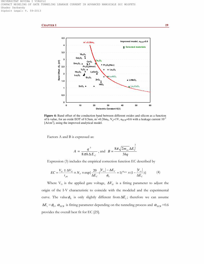
Figure 5: Band offset of the conduction band between different oxides and silicon as a function
of k-value, for an oxide EOT of 0.5nm, Vg=1V, J=10-2
[A/cm2], with effective mass m
*=0.20m0
and m*=0.50m0, using the improved analytical model.
It is not a very sensitive parameter since even for ECBα = 0.6 ± 0.3 we obtained very
small affects on the cE∆ -k plots, which means that with the improved model we can
select the same materials as a gate oxide dielectric than with the ECBα =0.6 case. NT
represents the behavior of density of carriers in the MOS structure [18, 19].
We have demonstrated that the potential barrier, dielectric constant value and the
electron effective mass variation are quite important when studying the gate material
that can be used. Figure 4 and Figure 5 show the guidelines for the selection of
alternative gate dielectrics by using our improved analytical model for high-
performance and low-operating-power logic technology requirements, assuming direct
tunneling current as a dominant current at an applied gate voltage of 1V, materials as
CeO2, LaAlO3, and La2CuO4 will be usable for EOT=0.5nm, leakage current J=0.01
[A/cm2], and m*=0.26m0.
UNIVERSITAT ROVIRA I VIRGILI COMPACT MODELING OF GATE TUNNELING LEAKAGE CURRENT IN ADVANCED NANOSCALE SOI MOSFETS Ghader Darbandy Dipòsit Legal: T. 59-2013
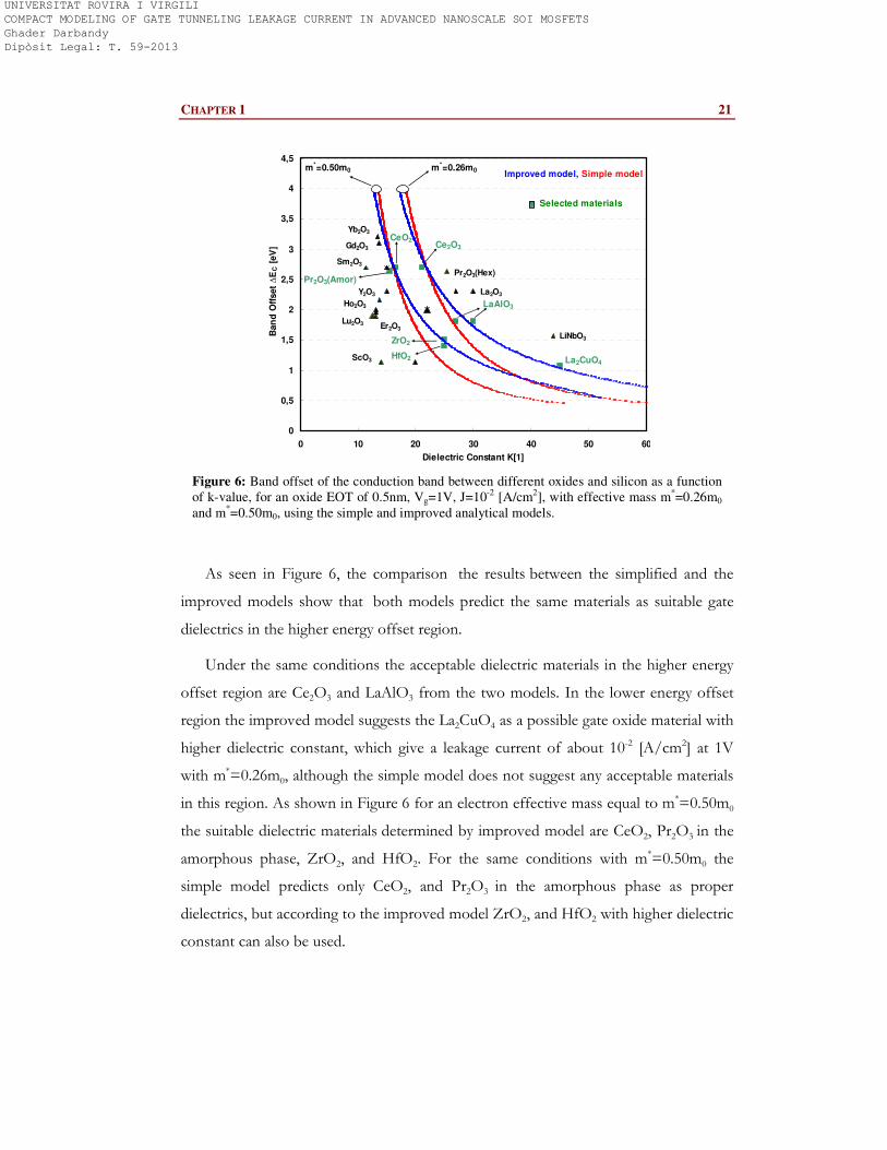
CHAPTER 1 21
La2O3
Ce2O3
CeO2
Pr2O3(Amor)Pr2O3(Hex)
Sm2O3
Gd2O3
Ho2O3
Er2O3
Yb2O3
Lu2O3
HfO2
Y2O3
ZrO2
LaAlO3
La2CuO4
LiNbO3
ScO3
0
0,5
1
1,5
2
2,5
3
3,5
4
4,5
0 10 20 30 40 50 60
Dielectric Constant K[1]
Ban
d O
ffset ∆
EC [
eV
]
m*=0.26m0Improved model, Simple model
m*=0.50m0
Selected materials
Figure 6: Band offset of the conduction band between different oxides and silicon as a function
of k-value, for an oxide EOT of 0.5nm, Vg=1V, J=10-2 [A/cm2], with effective mass m*=0.26m0
and m*=0.50m0, using the simple and improved analytical models.
As seen in Figure 6, the comparison the results between the simplified and the
improved models show that both models predict the same materials as suitable gate
dielectrics in the higher energy offset region.
Under the same conditions the acceptable dielectric materials in the higher energy
offset region are Ce2O3 and LaAlO3 from the two models. In the lower energy offset
region the improved model suggests the La2CuO4 as a possible gate oxide material with
higher dielectric constant, which give a leakage current of about 10-2 [A/cm2] at 1V
with m*=0.26m0, although the simple model does not suggest any acceptable materials
in this region. As shown in Figure 6 for an electron effective mass equal to m*=0.50m0
the suitable dielectric materials determined by improved model are CeO2, Pr2O3 in the
amorphous phase, ZrO2, and HfO2. For the same conditions with m*=0.50m0 the
simple model predicts only CeO2, and Pr2O3 in the amorphous phase as proper
dielectrics, but according to the improved model ZrO2, and HfO2 with higher dielectric
constant can also be used.
UNIVERSITAT ROVIRA I VIRGILI COMPACT MODELING OF GATE TUNNELING LEAKAGE CURRENT IN ADVANCED NANOSCALE SOI MOSFETS Ghader Darbandy Dipòsit Legal: T. 59-2013
22 GHADER DARBANDY
Actually, the improved model compare to the simple model gives additional
acceptable dielectric materials with higher dielectric constant for same conditions (see
in Figure 6).
4) Conclusion
We have developed analytical models for the gate tunneling leakage, adapted to DG
MOSFETs. Using the new models, we have estimated the novel high-k dielectric
materials that can work as gate oxides in DG device structures. Finally we have
presented guidelines for finding an appropriate material for the 22 nm low standby
power applications.
The simulations are based on two direct tunneling models of different complexity
in order to determine suitable new oxide materials for 22 nm with the conditions
EOT=0.5nm, J=0.01 [A/cm2] for gate leakage current at a gate voltage of 1V.
However both models give almost identical predictions in the range of k-values of
interest.
References
[1] H. Iwai, S. Ohmi, “Silicon integrated circuit technology from past to future”,
Microelectron Reliab, 2002; 42(4–5):465–91.
[2] J. Robertson, “High dielectric constant oxides”, Eur Phys J Appl Phys, 2004;
28(3):265–91.
[3]. J. Robertson, “Band offsets of wide-band-gap oxides and implications for future
electronic devices”, J. Vac. Sci. Technol. B 18, 1785 (2000).
[4] J. D. Plummer and P. B. Griffin, “Material and process limits in silicon VLSI
technology,” Proc. IEEE, vol. 89, pp. 240–258, Mar. 2001.
[5] E. J. Nowak, I. Aller, T. Ludwig, K. Kim, R. V. Joshi, Te Chuang-Ching, K.
Bernstein, R. Puri, “Turning silicon on its edge [double gate CMOS/FinFET
technology]”, IEEE Circ. Dev. Mag. Volume 20, Issue 1, Jan-Feb 2004 Page(s):20 – 31.
UNIVERSITAT ROVIRA I VIRGILI COMPACT MODELING OF GATE TUNNELING LEAKAGE CURRENT IN ADVANCED NANOSCALE SOI MOSFETS Ghader Darbandy Dipòsit Legal: T. 59-2013
CHAPTER 1 23
[6] Ching-Te Chuang, K. Bernstein, R. V. Joshi, R. Puri, K. Kim, E J. Nowak, T.
Ludwig, I. Aller. “Scaling planner silicon devices”, IEEE Circ. Dev. Mag. (2004) 6–18.
[7] L. Chang, K. J. Yang, Yeo. Yee-Chia, I. Polishchuk, Hu. Chenming, “Direct
tunneling gate leakage current in double-gate and ultrathin body MOSFETs”, IEEE,
TED 49 (2002) 2288–2295.
[8] K. F. Schuegraf and C. Hu, “Hole Injection SiO Breakdown model for very low
voltage lifetime extrapolation,” IEEE Trans. Electron Devices, vol. 41, no. 5, pp. 761–
767, 1994.
[9] R. Ludeke, E. Cartier, and A. Schenk, “Determination of the energy-dependent
conduction band mass in SiO2” Appl. Phys. Lett. 75, 1407 ~1999.
[10] Wu. Huixian, Zhao. Yijie(Sandy), H. White. Marvin, “Quantum mechanical
modeling of MOSFET gate leakage for high-k gate dielectrics”, Solid-State Electronics 50
(2006) 1164–1169.
[11] O. Engström, B. Raeissi, S. Hall, O. Buiu, MC. Lemme, H. D. B. Gottlob, P. K.
Hurley and K. Cherkaoui. “Navigation aids in the search for future high-k dielectrics:
physical and electrical trends”. Solid State Electron 2007; 51:622–6.
[12] T. Kauerauf, B. Govoreanu, R. Degraeve, G. Groeseneken, H. Maes. “Finding the
gate stack with the lowest leakage current”, Solid State Electron 2005; 49(5):695–701.
[13] M. Houssa, M. Tuominen, M. Naili, V. Afanas’ev, A. Stesmans, S. Haukka, M. M.
Heyns. “Trap-assisted tunneling in high permittivity gate dielectric stacks”. J Appl Phys
2000; 87(12):8615
[14] GD. Wilk, RM. Wallace, JM. Anthony. “High-k gate dielectrics: current status and
materials properties”. Appl Phys Rev 2001; 89(10):5243.
[15] A. Ghetti, E. Sangiorgi, J. Bude, T. W. Sorsch and Gary Weber “Tunneling into
Interface States as Reliability Monitor for Ultrathin Oxides” Trans. Electron Devices,
VOL.47, NO 12, DECEMBER 2000.
[16] F. Lime, G. Ghibaudo and G. Guegan, “Stress induced leakage current at low field
in ultra thin oxides” Microelectronics Reliability, 41 (2001) 1421-1425.
UNIVERSITAT ROVIRA I VIRGILI COMPACT MODELING OF GATE TUNNELING LEAKAGE CURRENT IN ADVANCED NANOSCALE SOI MOSFETS Ghader Darbandy Dipòsit Legal: T. 59-2013
24 GHADER DARBANDY
[17] K. F. Schuegraf and C. Hu, “Hole Injection SiO Breakdown model for very low
voltage lifetime extrapolation,” IEEE Trans, Electron Devices, vol. 41, no. 5, pp. 761–
767, 1994.
[18] A. Cerdeira, O. Moldovan, B. Iñiguez and M. Estrada, “Modeling of potentials
and threshold voltage for symmetric doped double-gate MOSFETs”, Solid-State
Electronics, vol. 52, no. 5, pp. 830-837, May 2008
[19] A. Cerdeira, B. Iñiguez and M. Estrada, “Compact model for short channel
symmetric doped double-gate MOSFET”, Solid-State Electronics, vol. 52, no. 7, pp. 1064-
1070, July 2008
[20] K. F. Schuegraf, C. C. King, and C. Hu, “Ultra-thin silicon dioxide leakage current
and scaling limit,” in Dig. Symp. VLSI, 1992, pp. 18–19.
[21] Yee. Chia, Yeo, Tsu. Jae. King, Chenming. Hu, “MOSFET gate leakage modeling
and selection guide for alternative gate dielectrics based on leakage considerations”.
IEEE Trans. on ED, vol. 50, no. 4, April 2003, p. 1027-1035.
[22] Francisco G. Ruiz · Andrés Godoy · Luca Donetti · I.M. Tienda-Luna ·Francisco
Gámiz · Carlos Sampedro “Accurate modeling of Metal/HfO2/Si capacitors”, J Comput
Electron 7:155–158 (2008).
[23] N. G. Tarr, D. L. Pulfrey, and D. S. Camporese, “An Analytic Model for the MIS
Tunnel Junction,” IEEE Trans. Electron Devices, vol. ED-30, no. ISSUE NO, pp. 1760–
1770, 1983.
[24] F. Rana, S. Tiwari, and D. A. Buchanan, “Self-consistent modeling of
accumulation layers and tunneling currents through very thin oxides,” Appl. Phys. Lett.,
vol. 69, no. 8, p. 1104, 1996.
[25] W-C. Lee, C. Hu. “Modeling CMOS tunneling currents through ultrathin gate
oxide due to conduction and valence-band electron and hole tunneling”. IEEE Trans
Electron Dev 2001; 48(7):1366-73.
[26] S. I. Garduño, A. Cerdeira M. Estrada, “Inclusion of Direct Tunneling Gate
Current in the Symmetric Doped Double Gate MOSFETs Model”, 2009 6th
International Conference on Electrical Engineering, Computing Science and Automatic Control
(CCE 2009).
UNIVERSITAT ROVIRA I VIRGILI COMPACT MODELING OF GATE TUNNELING LEAKAGE CURRENT IN ADVANCED NANOSCALE SOI MOSFETS Ghader Darbandy Dipòsit Legal: T. 59-2013
25
Chapter 2
Analytical Modeling of Direct Tunneling Current
through Gate Stacks for the Determination of Suitable
High-k Dielectric for Nanoscale Double-Gate
MOSFETs
Gate-leakage current reduction is the key motivation for the replacement of SiO2 with
alternative gate dielectrics. In this chapter, a guideline for the determination of the
suitable high-k candidate was reported in the case of a SiO2/high-k gate stack in
Nanoscale Double-Gate (DG) MOSFET. Analytical models of the direct tunneling
gate leakage current with SiO2 as an interfacial layer have been considered. Using these
models the most promising high-k materials for different conditions were predicted,
considering the effects of Equivalent Oxide Thickness (EOT), gate leakage current,
electron effective mass, dielectric constant-k value, barrier height and interfacial oxide
thickness.
UNIVERSITAT ROVIRA I VIRGILI COMPACT MODELING OF GATE TUNNELING LEAKAGE CURRENT IN ADVANCED NANOSCALE SOI MOSFETS Ghader Darbandy Dipòsit Legal: T. 59-2013
26 GHADER DARBANDY
1) Introduction
Alternative gate oxide materials with high dielectric constant candidates for coming
CMOS generations are one of the most challenging problems in the continuous
development of electronics [1]. Accurate characterization and modeling of the
tunneling current through gate stacks is essential to understand the scaling limitations
of gate dielectrics. Analytical models of the direct tunneling assumed to be main
component of the leakage current [2] through a trapezoidal barrier were considered to
study proper high-k candidates to meet the gate leakage requirements [3, 4].
In our previous work [5], the suitability of high-k dielectric for DG MOSFET at 22
nm technological node requirements was studied, assuming the ideal case without
interfacial layer between the dielectric and the Si body. However, in order to maintain a
good interface and to prevent mobility degradation, it is desirable to have a thin layer
of SiO2 between the bulk and the high-k dielectric [6, 7].
In this chapter, accurate simplified and improved models for the direct tunneling
current through SiO2/high-k gate stacks are presented for the determination of suitable
high-k dielectrics for Nanoscale DG MOSFETs. The direct tunneling models are
adapted to our previous DG MOSFET compact model for the potential and drain
current [8, 9]. Using these models, the most important parameters like: gate leakage
current, EOT, electron effective mass, dielectric constant-k value, energy band-offset
values between the conduction band of the oxide and the silicon substrate (barrier
height) and interfacial oxide thickness are studied. Then, the most promising gate oxide
materials for further DG MOSFETs technologies are highlighted from considered
parameters point of view.
UNIVERSITAT ROVIRA I VIRGILI COMPACT MODELING OF GATE TUNNELING LEAKAGE CURRENT IN ADVANCED NANOSCALE SOI MOSFETS Ghader Darbandy Dipòsit Legal: T. 59-2013
CHAPTER 2 27
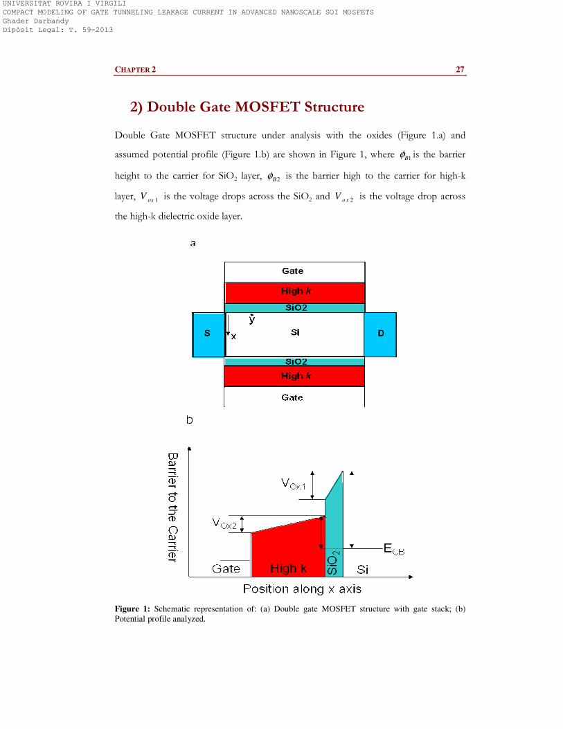
2) Double Gate MOSFET Structure
Double Gate MOSFET structure under analysis with the oxides (Figure 1.a) and
assumed potential profile (Figure 1.b) are shown in Figure 1, where 1Bφ is the barrier
height to the carrier for SiO2 layer, 2Bφ is the barrier high to the carrier for high-k
layer, 1oxV is the voltage drops across the SiO2 and 2o xV is the voltage drop across
the high-k dielectric oxide layer.
Figure 1: Schematic representation of: (a) Double gate MOSFET structure with gate stack; (b)
Potential profile analyzed.
UNIVERSITAT ROVIRA I VIRGILI COMPACT MODELING OF GATE TUNNELING LEAKAGE CURRENT IN ADVANCED NANOSCALE SOI MOSFETS Ghader Darbandy Dipòsit Legal: T. 59-2013
28 GHADER DARBANDY
The electric field at the surfaces of the Si-SiO2 and SiO2-high-k materials is needed
in order to model gate leakage tunneling current for DG MOSFET structure. In our
previous works an explicit compact model for the surface potential and drain current
including short channel effects for DG MOSFET transistor was developed [8, 9].
Using this potential model in order to model gate leakage current, the electric field at
the surface of the Si-SiO2 ( SE ) was calculated using Poisson’s equation. The following
expression was obtained for SE as a function of the potential at the surface Sφ and at
the center of the Si film oφ [8, 9]:
2( ) ( )2
( ) (1 )
S O S F
t t
V
a t S OS
s t
qNE e e
φ φ φ φ
φ φφ φ φ
ε φ
− − −−−
= × + − × (1)
where ' /t KT qφ = is the thermal potential, K is the Boltzmann constant, q is the
electron charge, 'T is the temperature in Kelvin, Na is the uniform acceptor
concentration in the silicon layer, Fpφ is the quasi Fermi level for holes in the P-type
silicon layer, and Fnφ is the quasi Fermi level for electrons. The potential along the
channel is Fn FpV φ φ= − , and Fpφ is renamed as Fφ [8, 9].
Figure 2 shows surface potential at the Si-SiO2 interface obtained from the model
of [8, 9] are in a good agreement with those obtained from ATLAS numerical
simulations for DG MOSFET structure.
UNIVERSITAT ROVIRA I VIRGILI COMPACT MODELING OF GATE TUNNELING LEAKAGE CURRENT IN ADVANCED NANOSCALE SOI MOSFETS Ghader Darbandy Dipòsit Legal: T. 59-2013
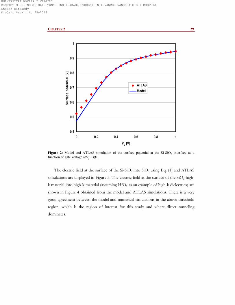
CHAPTER 2 29
0.4
0.5
0.6
0.7
0.8
0.9
1
0 0.2 0.4 0.6 0.8 1
Vg [V]
Su
rfa
ce
po
ten
tia
l [v
]
ATLAS
Model
Figure 2: Model and ATLAS simulation of the surface potential at the Si-SiO2 interface as a
function of gate voltage at 0d
V V= .
The electric field at the surface of the Si-SiO2 into SiO2 using Eq. (1) and ATLAS
simulations are displayed in Figure 3. The electric field at the surface of the SiO2-high-
k material into high-k material (assuming HfO2 as an example of high-k dielectrics) are
shown in Figure 4 obtained from the model and ATLAS simulations. There is a very
good agreement between the model and numerical simulations in the above threshold
region, which is the region of interest for this study and where direct tunneling
dominates.
UNIVERSITAT ROVIRA I VIRGILI COMPACT MODELING OF GATE TUNNELING LEAKAGE CURRENT IN ADVANCED NANOSCALE SOI MOSFETS Ghader Darbandy Dipòsit Legal: T. 59-2013
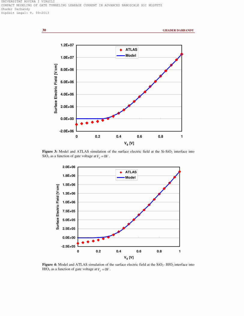
30 GHADER DARBANDY
-2.0E+06
0.0E+00
2.0E+06
4.0E+06
6.0E+06
8.0E+06
1.0E+07
1.2E+07
0 0.2 0.4 0.6 0.8 1
Vg [V]
Su
rface E
lectr
ic F
ield
[V
/cm
]
ATLAS
Model
Figure 3: Model and ATLAS simulation of the surface electric field at the Si-SiO2 interface into
SiO2 as a function of gate voltage at 0d
V V= .
-2.5E+05
0.0E+00
2.5E+05
5.0E+05
7.5E+05
1.0E+06
1.3E+06
1.5E+06
1.8E+06
2.0E+06
0 0.2 0.4 0.6 0.8 1
Vg [V]
Su
rface E
lectr
ic F
ield
[V
/cm
]
ATLAS
Model
Figure 4: Model and ATLAS simulation of the surface electric field at the SiO2- HfO2 interface into
HfO2 as a function of gate voltage at 0dV V= .
UNIVERSITAT ROVIRA I VIRGILI COMPACT MODELING OF GATE TUNNELING LEAKAGE CURRENT IN ADVANCED NANOSCALE SOI MOSFETS Ghader Darbandy Dipòsit Legal: T. 59-2013
CHAPTER 2 31
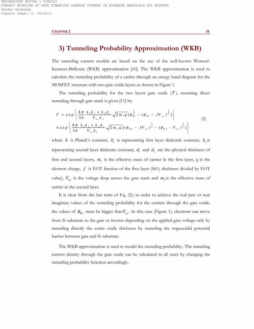
3) Tunneling Probability Approximation (WKB)
The tunneling current models are based on the use of the well-known Wentzel-
Kramers-Brillouin (WKB) approximation [10]. The WKB approximation is used to
calculate the tunneling probability of a carrier through an energy band diagram for the
MOSFET structure with two gate oxide layers as shown in Figure 1.
The tunneling probability for the two layers gate oxide (T ), assuming direct
tunneling through gate stack is given [11] by:
3 3
1 2 2 1 2 21 1 1
2
3 3
1 2 2 1 2 22 2 2
1
8e x p 2 [ ( ) ]
3
8e x p 2 [ ( ) ( ) ]
3
B B o x
o x
B o x B o x
o x
k d k dT m q f V
h V k
k d k dm q f V V
h V k
πφ φ
πφ φ
+= − −
+× − − −
(2)
where h is Planck’s constant, 1k is representing first layer dielectric constant, 2k is
representing second layer dielectric constant, 1d and
2d are the physical thickness of
first and second layers, 1m is the effective mass of carrier in the first layer, q is the
electron charge, f is EOT fraction of the first layer (SiO2 thickness divided by EOT
value), oxV is the voltage drop across the gate stack and
2m is the effective mass of
carrier in the second layer.
It is clear from the last term of Eq. (2); in order to achieve the real part or non
imaginary values of the tunneling probability for the carriers through the gate oxide,
the values of 2Bφ must be bigger than oxV . In this case (Figure 1), electrons can move
from Si substrate to the gate or inverse depending on the applied gate voltage only by
tunneling directly the entire oxide thickness by tunneling the trapezoidal potential
barrier between gate and Si substrate.
The WKB approximation is used to model the tunneling probability. The tunneling
current density through the gate oxide can be calculated in all cases by changing the
tunneling probability function accordingly.
UNIVERSITAT ROVIRA I VIRGILI COMPACT MODELING OF GATE TUNNELING LEAKAGE CURRENT IN ADVANCED NANOSCALE SOI MOSFETS Ghader Darbandy Dipòsit Legal: T. 59-2013
32 GHADER DARBANDY
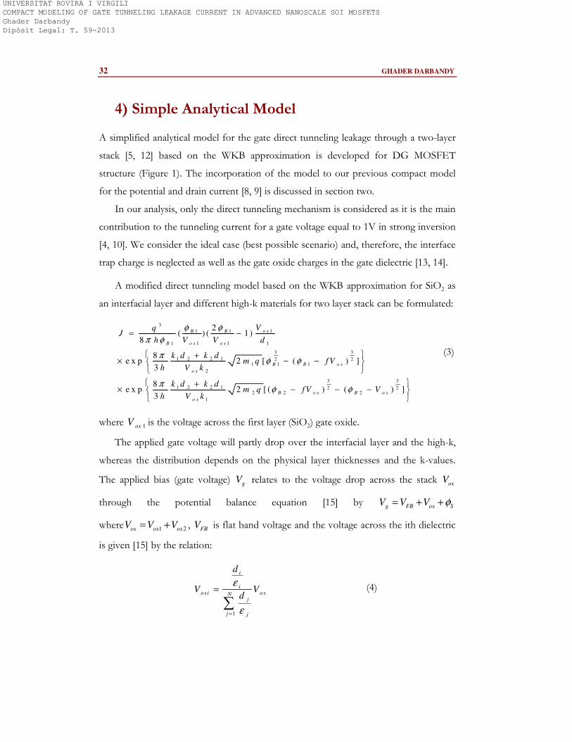
4) Simple Analytical Model
A simplified analytical model for the gate direct tunneling leakage through a two-layer
stack [5, 12] based on the WKB approximation is developed for DG MOSFET
structure (Figure 1). The incorporation of the model to our previous compact model
for the potential and drain current [8, 9] is discussed in section two.
In our analysis, only the direct tunneling mechanism is considered as it is the main
contribution to the tunneling current for a gate voltage equal to 1V in strong inversion
[4, 10]. We consider the ideal case (best possible scenario) and, therefore, the interface
trap charge is neglected as well as the gate oxide charges in the gate dielectric [13, 14].
A modified direct tunneling model based on the WKB approximation for SiO2 as
an interfacial layer and different high-k materials for two layer stack can be formulated:
3
11 1
1 1 1 1
3 3
1 2 2 1 2 21 1 1
2
3 3
1 2 2 1 2 22 2 2
1
2( ) ( 1 )
8
8e x p 2 [ ( ) ]
3
8e x p 2 [ ( ) ( ) ]
3
o xB B
B o x o x
B B o x
o x
B o x B o x
o x
VqJ
h V V d
k d k dm q f V
h V k
k d k dm q f V V
h V k
φ φ
π φ
πφ φ
πφ φ
= −
+× − −
+× − − −
(3)
where 1oxV is the voltage across the first layer (SiO2) gate oxide.
The applied gate voltage will partly drop over the interfacial layer and the high-k,
whereas the distribution depends on the physical layer thicknesses and the k-values.
The applied bias (gate voltage) gV relates to the voltage drop across the stack oxV
through the potential balance equation [15] by g FB ox SV V V φ= + +
where 1 2ox ox oxV V V= + , FBV is flat band voltage and the voltage across the ith dielectric
is given [15] by the relation:
1
i
ioxi oxN
j
j j
d
V Vd
ε
ε=
=
∑ (4)
UNIVERSITAT ROVIRA I VIRGILI COMPACT MODELING OF GATE TUNNELING LEAKAGE CURRENT IN ADVANCED NANOSCALE SOI MOSFETS Ghader Darbandy Dipòsit Legal: T. 59-2013
CHAPTER 2 33
iε being the permittivity of the ith gate dielectric layer.
The considered direct tunneling model is used to study the most interesting high-k
dielectric candidates for gate leakage requirements.
5) Improved Analytical Model
The simple model expression includes a number of approximations that lead to
inaccuracies (e.g., the assumption of a constant effective mass for all energies). As the
oxide becomes thinner, the quantization effects in the semiconductor have to be
considered in order to obtain the oxide potentials as an accurate function of the gate
voltage [16, 17]. Therefore, a correction function (C ) is needed in order to cover these
effects in an analytical model. This leads to an improved analytical model [12, 18].
An improved analytical model based on the proper WKB approximation in order
to accurately model the direct tunneling gate leakage current, by considering semi
empirical correction function, can be proposed:
3 33
1 2 2 1 2 21 1 1
1 1 2
3 3
1 2 2 1 2 22 2 2
1
8exp 2 [ ( ) ]
8 3
8exp 2 [( ) ( ) ]
3
B B ox
B ox
B ox B ox
ox
k d k dq CJ m q fV
h h V k
k d k dm q fV V
h V k
πφ φ
π φ ε
πφ φ
+= − −
+× − − −
(5)
where 1ε is SiO2 permittivity and C is the semi empirical corrections function:
1 1 1
1 1 0 1
2 0. . e x p { ( 1) (1 )}E C B
g g o x B o x
T
B B
V V V VC N
d
αφ
φ φ φ
± ∆ −= + × − (6)
GV∆ is a fitting parameter to adjust the origin of the I V− characteristic to make the
modeled curve coincide with the experimental curve [12], its value is the same in all
calculations. The value 0φ is only slightly different from 1Bφ ( 0 1Bφ φ≈ ), ECBα is a fitting
UNIVERSITAT ROVIRA I VIRGILI COMPACT MODELING OF GATE TUNNELING LEAKAGE CURRENT IN ADVANCED NANOSCALE SOI MOSFETS Ghader Darbandy Dipòsit Legal: T. 59-2013
34 GHADER DARBANDY
0.0E+00
5.0E-06
1.0E-05
1.5E-05
2.0E-05
2.5E-05
3.0E-05
0 0.2 0.4 0.6 0.8 1
Vg [V]
I g [
A]
Atlas
model
Figure 5: Analytical model and ATLAS simulations for the gate leakage tunneling current for DG
MOSFET with EOT=0.5nm, 0dV V= , interfacial layer (SiO2) thickness of 0.2nm and HfO2 as an
oxide material.
parameter depending on the tunneling process and TN represents the density of
carriers for depletion, inversion and accumulation regimes in the injecting electrode
[12, 18].
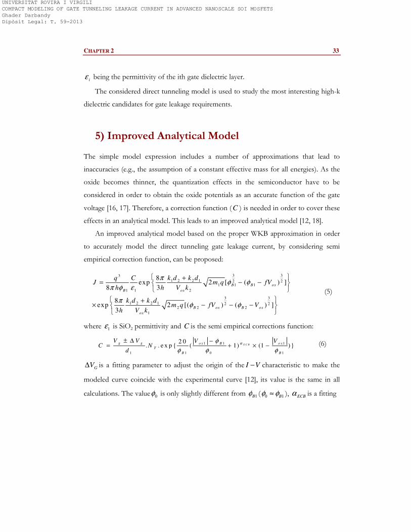
Figure 5 demonstrates the accuracy of the direct tunneling gate leakage current as
function of gate voltage at 0dV = obtained by the model and ATLAS simulation.
There is a very good agreement at high gate voltage (maximum gate leakage current).
6) Results and Discussion
Modified simple and improved direct tunneling models based on the WKB
approximation are used to study the 2k , 2Bφ , EOT, 1d , and 2m dependence of the gate
leakage current in order to study suitability of high-k materials while 1 3.2Bφ = eV and
1 00.50m m= ( 0m is the free electron mass) [7]. To select the alternative materials, it is
UNIVERSITAT ROVIRA I VIRGILI COMPACT MODELING OF GATE TUNNELING LEAKAGE CURRENT IN ADVANCED NANOSCALE SOI MOSFETS Ghader Darbandy Dipòsit Legal: T. 59-2013
CHAPTER 2 35
important to notice that as the dielectric constant of the material increase, the band gap
decreases and therefore higher k dielectrics tend to have a lower barrier height [19, 20].
Using the models, the optimum candidates are shown for each condition in order to
meet the gate leakage requirements ( 2Bφ is shown as a band offset CE∆ in the figures).
A) Simple Model
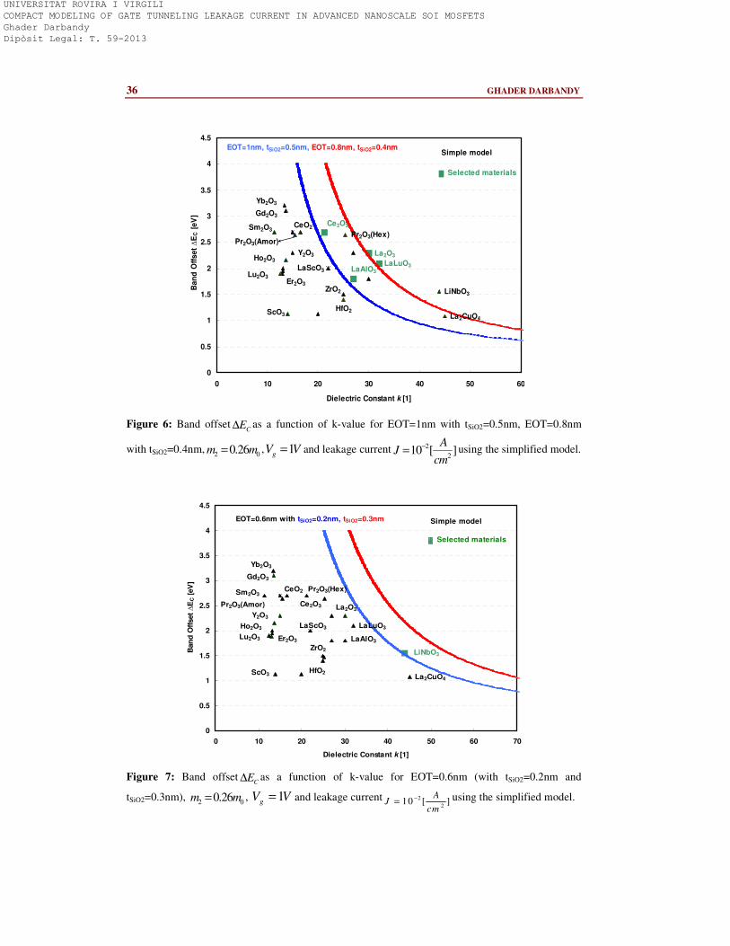
In order to study the effect of EOT and interfacial oxide thickness on the gate oxide
materials, we have carried out the calculation by varying the EOT and SiO2 thickness
while maintaining the same leakage current ( 2
210 [ ]
AJ
cm
−= ) and gate voltage 1V for
the device. Figure 6 and Figure 7 illustrate, with decreasing of EOT and SiO2
thickness, the gate oxide materials change.
The proposed model determines the suitable dielectric materials as a gate oxide for
the two layers case with EOT=0.6nm,2 00.26m m= , 1gV V= , the gate leakage
current 2
210 [ ]
AJ
cm
−= , two different SiO2 thicknesses as 1 10.2 , 0.3d nm d nm= = for
the nanoscale DG MOSFETs requirement parameters regarding to the low standby
power application (Figure 7). The curve is plotted for different SiO2 thickness and it
shows the trend of the curves with interfacial layer thickness. The comparison can
theoretically help to select available high-k dielectrics and suitable interfacial layer
thickness.
It is found that Ce2O3 and LaAlO3 are suitable gate oxides for EOT = 1 nm with a
SiO2 thickness equal to 0.5 nm (Figure 6) and that the use of La2O3 and LaLuO3
dielectric materials leads to good results for EOT = 0.8 nm and 1 0.4d nm= (Figure 6).
Moreover, LiNbO3 is found to be a suitable gate oxide for EOT=0.6nm with a SiO2
thickness equal to 0.2 nm (Figure 7). On the other hand, for EOT = 0.6 nm and SiO2
thickness equal to 0.3 nm (Figure 7), no suitable dielectric materials are found using the
simplified model. Additionally, it can be noticed (Figs. 6 and 7) that when decreasing
the EOT and the SiO2 interfacial thickness, the suitable gate oxide materials zone
changes drastically due to the total physical thickness change.
UNIVERSITAT ROVIRA I VIRGILI COMPACT MODELING OF GATE TUNNELING LEAKAGE CURRENT IN ADVANCED NANOSCALE SOI MOSFETS Ghader Darbandy Dipòsit Legal: T. 59-2013
36 GHADER DARBANDY
La2O3
Ce2O3CeO2
Pr2O3(Amor)Pr2O3(Hex)
Sm2O3
Gd2O3
Ho2O3
Er2O3
Yb2O3
Lu2O3
HfO2
Y2O3
ZrO2
LaAlO3
La2CuO4
LiNbO3
LaScO3
ScO3
LaLuO3
0
0.5
1
1.5
2
2.5
3
3.5
4
4.5
0 10 20 30 40 50 60
Dielectric Constant k [1]
Ba
nd
Off
se
t ∆
EC
[e
V]
Simple model
Selected materials
EOT=1nm, tSiO2=0.5nm, EOT=0.8nm, tSiO2=0.4nm
Figure 6: Band offsetC
E∆ as a function of k-value for EOT=1nm with tSiO2=0.5nm, EOT=0.8nm
with tSiO2=0.4nm,2 00.26m m= , 1
gV V= and leakage current 2
210 [ ]
AJ
cm
−= using the simplified model.
La2O3Ce2O3
CeO2
Pr2O3(Amor)
Pr2O3(Hex)Sm2O3
Gd2O3
Ho2O3
Er2O3
Yb2O3
Lu2O3
HfO2
Y2O3
ZrO2
LaAlO3
La2CuO4
LiNbO3
LaScO3
ScO3
LaLuO3
0
0.5
1
1.5
2
2.5
3
3.5
4
4.5
0 10 20 30 40 50 60 70
Dielectric Constant k [1]
Ban
d O
ffset ∆
EC [
eV
]
Simple model
Selected materials
EOT=0.6nm with tSiO2=0.2nm, tSiO2=0.3nm
Figure 7: Band offsetCE∆ as a function of k-value for EOT=0.6nm (with tSiO2=0.2nm and
tSiO2=0.3nm), 2 00.26m m= , 1gV V= and leakage current 2
210 [ ]
AJ
cm
−= using the simplified model.
UNIVERSITAT ROVIRA I VIRGILI COMPACT MODELING OF GATE TUNNELING LEAKAGE CURRENT IN ADVANCED NANOSCALE SOI MOSFETS Ghader Darbandy Dipòsit Legal: T. 59-2013
CHAPTER 2 37
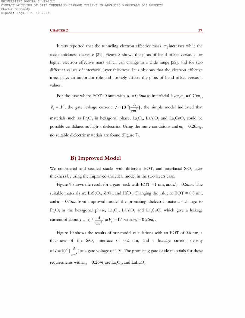
It was reported that the tunneling electron effective mass 2m increases while the
oxide thickness decrease [21]. Figure 8 shows the plots of band offset versus k for
higher electron effective mass which can change in a wide range [22], and for two
different values of interfacial layer thickness. It is obvious that the electron effective
mass plays an important role and strongly affects the plots of band offset versus k
values.
For the case where EOT=0.6nm with 1 0.3d nm= as interfacial layer,
2 00.70m m= ,
1gV V= , the gate leakage current 2
210 [ ]
AJ
cm
−= , the simple model indicated that
materials such as Pr2O3 in hexagonal phase, La2O3, LaAlO3 and La2CuO4 could be
possible candidates as high-k dielectrics. Using the same conditions and 2 00.26m m= ,
no suitable dielectric materials are found (Figure 7).
B) Improved Model
We considered and studied stacks with different EOT, and interfacial SiO2 layer
thickness by using the improved analytical model in the two layers case.
Figure 9 shows the result for a gate stack with EOT =1 nm, and 1 0.5d nm= . The
suitable materials are LaScO3, ZrO2, and HfO2. Changing the value to EOT = 0.8 nm,
and1 0.4d nm= from improved model the promising dielectric materials change to
Pr2O3 in the hexagonal phase, La2O3, LaAlO3 and La2CuO4 which give a leakage
current of about 2
210 [ ]
AJ
cm
−= at 1gV V= with2 00.26m m= .
Figure 10 shows the results of our model calculations with an EOT of 0.6 nm, a
thickness of the SiO2 interface of 0.2 nm, and a leakage current density
of 2
210 [ ]
AJ
cm
−= at a gate voltage of 1 V. The promising gate oxide materials for these
requirements with 2 00.26m m= are La2O3, and LaLuO3.
UNIVERSITAT ROVIRA I VIRGILI COMPACT MODELING OF GATE TUNNELING LEAKAGE CURRENT IN ADVANCED NANOSCALE SOI MOSFETS Ghader Darbandy Dipòsit Legal: T. 59-2013
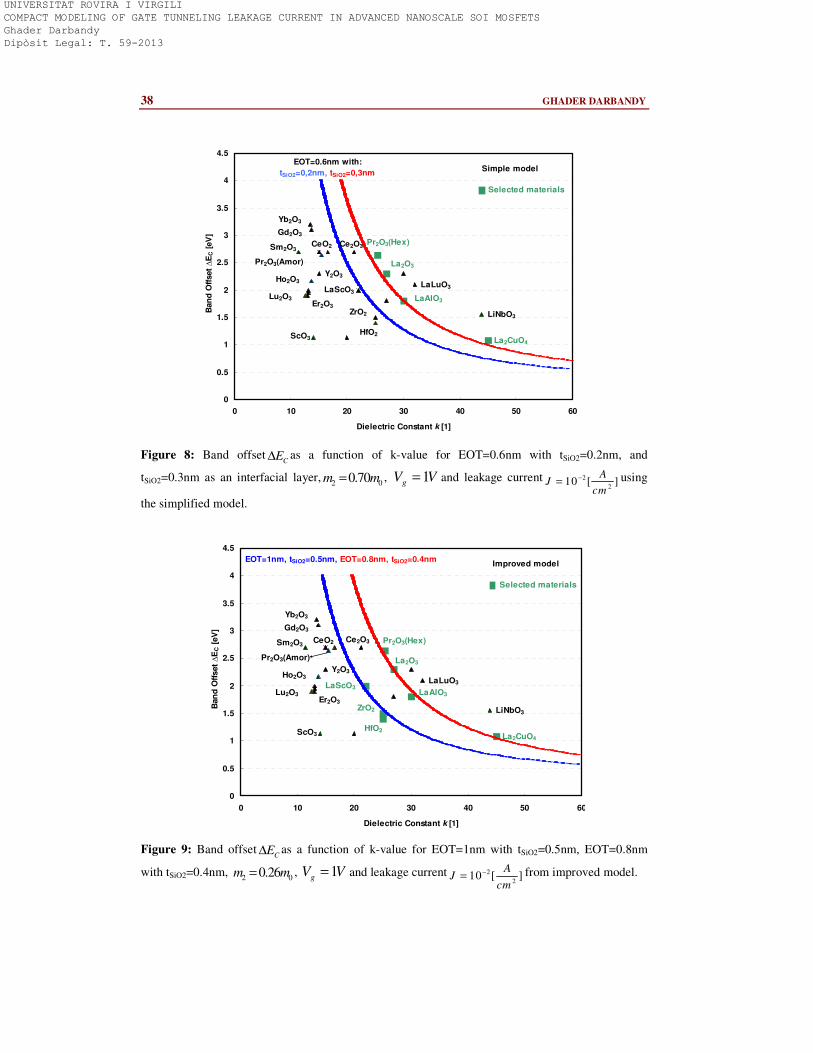
38 GHADER DARBANDY
La2O3
Ce2O3CeO2
Pr2O3(Amor)
Pr2O3(Hex)Sm2O3
Gd2O3
Ho2O3
Er2O3
Yb2O3
Lu2O3
HfO2
Y2O3
ZrO2
LaAlO3
La2CuO4
LiNbO3
LaScO3
ScO3
LaLuO3
0
0.5
1
1.5
2
2.5
3
3.5
4
4.5
0 10 20 30 40 50 60
Dielectric Constant k [1]
Ban
d O
ffset ∆
EC [
eV
]
Simple model
Selected materials
EOT=0.6nm with:
tSiO2=0,2nm, tSiO2=0,3nm
Figure 8: Band offsetCE∆ as a function of k-value for EOT=0.6nm with tSiO2=0.2nm, and
tSiO2=0.3nm as an interfacial layer,2 00.70m m= , 1gV V= and leakage current 2
210 [ ]
AJ
cm
−= using
the simplified model.
La2O3
Ce2O3CeO2
Pr2O3(Amor)
Pr2O3(Hex)Sm2O3
Gd2O3
Ho2O3
Er2O3
Yb2O3
Lu2O3
HfO2
Y2O3
ZrO2
LaAlO3
La2CuO4
LiNbO3
LaScO3
ScO3
LaLuO3
0
0.5
1
1.5
2
2.5
3
3.5
4
4.5
0 10 20 30 40 50 60
Dielectric Constant k [1]
Ban
d O
ffset ∆
EC [
eV
]
Improved model
Selected materials
EOT=1nm, tSiO2=0.5nm, EOT=0.8nm, tSiO2=0.4nm
Figure 9: Band offsetC
E∆ as a function of k-value for EOT=1nm with tSiO2=0.5nm, EOT=0.8nm
with tSiO2=0.4nm, 2 00.26m m= , 1gV V= and leakage current 2
210 [ ]
AJ
cm
−= from improved model.
UNIVERSITAT ROVIRA I VIRGILI COMPACT MODELING OF GATE TUNNELING LEAKAGE CURRENT IN ADVANCED NANOSCALE SOI MOSFETS Ghader Darbandy Dipòsit Legal: T. 59-2013
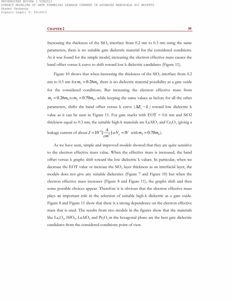
CHAPTER 2 39
Increasing the thickness of the SiO2 interface from 0.2 nm to 0.3 nm using the same
parameters, there is no suitable gate dielectric material for the considered conditions.
As it was found for the simple model, increasing the electron effective mass causes the
band offset versus k curve to shift toward low k dielectric candidates (Figure 11).
Figure 10 shows that when increasing the thickness of the SiO2 interface from 0.2
nm to 0.3 nm for 2 00.26m m= , there is no dielectric material possibility as a gate oxide
for the considered conditions. But increasing the electron effective mass from
2 00.26m m= to 2 00.70m m= , while keeping the same values as before for all the other
parameters, shifts the band offset versus k curve ( cE k∆ − ) toward low dielectric k
value as it can be seen in Figure 11. For gate stacks with EOT = 0.6 nm and SiO2
thickness equal to 0.3 nm, the suitable high-k materials are LaAlO3 and Ce2O3 (giving a
leakage current of about 2
210 [ ]
AJ
cm
−= at 1gV V= with 2 00.70m m= ).
As we have seen, simple and improved models showed that they are quite sensitive
to the electron effective mass value. When the effective mass is increased, the band
offset versus k graphs shift toward the low dielectric k values. In particular, when we
decrease the EOT value or increase the SiO2 layer thickness as an interfacial layer, the
models does not give any suitable dielectrics (Figure 7 and Figure 10) but when the
electron effective mass increases (Figure 8 and Figure 11), the graphs shift and then
some possible choices appear. Therefore it is obvious that the electron effective mass
plays an important role in the selection of suitable high-k dielectric as a gate oxide.
Figure 8 and Figure 11 show that there is a strong dependence on the electron effective
mass that is used. The results from two models in the figures show that the materials
like La2O3, HfO2, LaAlO3 and Pr2O3 in the hexagonal phase are the best gate dielectric
candidates from the considered conditions point of view.
UNIVERSITAT ROVIRA I VIRGILI COMPACT MODELING OF GATE TUNNELING LEAKAGE CURRENT IN ADVANCED NANOSCALE SOI MOSFETS Ghader Darbandy Dipòsit Legal: T. 59-2013
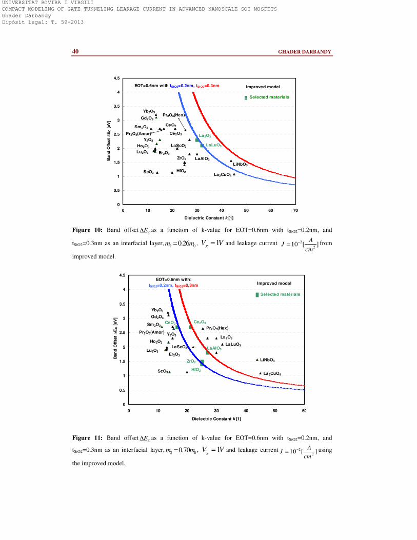
40 GHADER DARBANDY
La2O3Ce2O3
CeO2
Pr2O3(Amor)
Pr2O3(Hex)
Sm2O3
Gd2O3
Ho2O3
Er2O3
Yb2O3
Lu2O3
HfO2
Y2O3
ZrO2 LaAlO3
La2CuO4
LiNbO3
LaScO3
ScO3
LaLuO3
0
0.5
1
1.5
2
2.5
3
3.5
4
4.5
0 10 20 30 40 50 60 70
Dielectric Constant k [1]
Ban
d O
ffset ∆
EC [
eV
]
Improved model
Selected materials
EOT=0.6nm with tSiO2=0.2nm, tSiO2=0.3nm
Figure 10: Band offsetC
E∆ as a function of k-value for EOT=0.6nm with tSiO2=0.2nm, and
tSiO2=0.3nm as an interfacial layer,2 00.26m m= , 1gV V= and leakage current 2
210 [ ]
AJ
cm
−= from
improved model.
La2O3
Ce2O3CeO2
Pr2O3(Amor)Pr2O3(Hex)
Sm2O3
Gd2O3
Ho2O3
Er2O3
Yb2O3
Lu2O3
HfO2
Y2O3
ZrO2
LaAlO3
La2CuO4
LiNbO3
LaScO3
ScO3
LaLuO3
0
0.5
1
1.5
2
2.5
3
3.5
4
4.5
0 10 20 30 40 50 60
Dielectric Constant k [1]
Ban
d O
ffset ∆
EC [
eV
]
Improved model
Selected materials
EOT=0.6nm with:
tSiO2=0,2nm, tSiO2=0,3nm
Figure 11: Band offsetC
E∆ as a function of k-value for EOT=0.6nm with tSiO2=0.2nm, and
tSiO2=0.3nm as an interfacial layer,2 00.70m m= , 1gV V= and leakage current 2
210 [ ]
AJ
cm
−= using
the improved model.
UNIVERSITAT ROVIRA I VIRGILI COMPACT MODELING OF GATE TUNNELING LEAKAGE CURRENT IN ADVANCED NANOSCALE SOI MOSFETS Ghader Darbandy Dipòsit Legal: T. 59-2013
CHAPTER 2 41
7) Conclusion
Analytical models for the direct tunneling current flowing between gate and channel,
based on the modified WKB tunneling probability approximation through the gate
stack have been developed. The models have been used to study the impact of
parameters in the leakage current equations in order to find guidelines for the search of
an appropriate dielectric in Nanoscale DG MOSFET structure.
It should be noted that the EOT, barrier height, dielectric constant-k value,
interfacial layer thickness and electron effective mass strongly affect the direct
tunneling current and they should be considered together in determining the suitable
dielectrics. The models show the most promising high-k candidates for different values
of EOT and SiO2 interfacial layer thickness, satisfying the gate leakage requirements.
They demonstrate that the materials like La2O3, HfO2, LaAlO3 and Pr2O3 in the
hexagonal phase would fulfill the considered requirements.
References
[1] H. Iwai, S. Ohmi, “Silicon integrated circuit technology from past to future”,
Microelectron Reliab, 2002; 42(4–5):465–91.
[2] T. Kauerauf, B. Govoreanu, R. Degraeve, G. Groeseneken, H. Maes. “Finding the
gate stack with the lowest leakage current”, Solid State Electron, 2005; 49(5):695–701.
[3] K. F. Schuegraf, C. C. King, and C. Hu, “Ultra-thin silicon dioxide leakage current
and scaling limit,” in Dig. of VLSI Symp., 1992, pp. 18–19.
[4] K. F. Schuegraf and C. Hu, “Hole Injection SiO Breakdown model for very low
voltage lifetime extrapolation,” IEEE Trans. Electron Devices, vol. 41, no. 5, pp. 761–
767, 1994.
[5] Ghader Darbandy, Romain Ritzenthaler, Francois Lime, Ivan Garduño, Magali
Estrada, Antonio Cerdeira and Benjamin Iñiguez, “Analytical Modeling of the Gate
Tunneling Leakage for the Determination of Adequate High-K Dielectrics in 22 nm
Double-Gate SOI MOSFETs”, Solid-State Electronics, 54 (2010) 1083-1087.
UNIVERSITAT ROVIRA I VIRGILI COMPACT MODELING OF GATE TUNNELING LEAKAGE CURRENT IN ADVANCED NANOSCALE SOI MOSFETS Ghader Darbandy Dipòsit Legal: T. 59-2013
42 GHADER DARBANDY
[6] Ghader Darbandy, Romain Ritzenthaler, Francois Lime, Ivan Garduño, Magali
Estrada, Antonio Cerdeira and Benjamin Iñiguez, “Analytical Modeling of Direct
Tunnelling Current through SiO2/high-k Gate Stacks for the Determination of
Suitable High-k Dielectrics for Nanoscale Double-Gate MOSFETs”, (EUROSOI
2010), Grenoble, France (January 25-27 2010).
[7] J. Robertson, “High dielectric constant oxides”, Eur Phys J Appl Phys, 2004;
28(3):265–91.
[8] A. Cerdeira, O. Moldovan, B. Iñiguez and M. Estrada, “Modeling of potentials and
threshold voltage for symmetric doped double-gate MOSFETs”, Solid-State Electronics,
vol. 52, no. 5, pp. 830-837, 2008.
[9] A. Cerdeira, B. Iñiguez and M. Estrada, “Compact model for short channel
symmetric doped double-gate MOSFET,”, Solid-State Electronics, vol. 52, no. 7, pp.
1064-1070, July 2008.
[10] Eugen. Merzbacher, Quantum mechanics, John Wiley & Sons, New York; 1961,
1970.
[11] Mohan V. Dunga, Xuemei Xi, Jin He, Igor Polishchuk, Qiang Lu, Mansun Chan,
Ali M. Niknejad, and Chenming Hu “Modeling of Direct Tunneling Current in Multi-
Layer Gate Stacks”, Nanotech 2003, Vol. 2, www.nsti.org, ISBN 0-9728422-1-7.
[12] S. I. Garduño, A. Cerdeira M. Estrada, “Inclusion of Direct Tunneling Gate
Current in the Symmetric Doped Double Gate MOSFETs Model”, 2009 6th
International Conference on Electrical Engineering, Computing Science and Automatic Control
(CCE 2009).
[13] M. Houssa, M. Tuominen, M. Naili, V. Afanas’ev, A. Stesmans, S. Haukka, M. M.
Heyns. “Trap-assisted tunneling in high permittivity gate dielectric stacks”. J Appl Phys
2000; 87(12):8615.
[14] GD. Wilk, RM. Wallace, JM. Anthony. “High-k gate dielectrics: current status and
materials properties”. Appl Phys Rev 2001; 89(10):5243.
[15] Hitender Kumar Tyagi, P. J. George “Tunneling currents through ultra thin
HfO2/Al2O3/HfO2 triple layer gate dielectrics for advanced MIS devices” J mater Sci:
Mater Electron (2008) 19:902-907.
UNIVERSITAT ROVIRA I VIRGILI COMPACT MODELING OF GATE TUNNELING LEAKAGE CURRENT IN ADVANCED NANOSCALE SOI MOSFETS Ghader Darbandy Dipòsit Legal: T. 59-2013
CHAPTER 2 43
[16] N. G. Tarr, D. L. Pulfrey, and D. S. Camporese, “An Analytic Model for the MIS
Tunnel Junction,” IEEE Trans. Electron Devices, vol. ED-30, No. 12, pp. 1760–1770,
1983.
[17] F. Rana, S. Tiwari, and D. A. Buchanan, “Self-consistent modeling of
accumulation layers and tunneling currents through very thin oxides,” Appl. Phys. Lett.,
vol. 69, no. 8, p. 1104, 1996.
[18] W-C. Lee, C. Hu. “Modeling CMOS tunneling currents through ultrathin gate
oxide due to conduction and valence-band electron and hole tunneling” IEEE Trans
Electron Dev 2001; 48(7):1366-73.
[19] J. Robertson, “Band offsets of wide-band-gap oxides and implications for future
electronic devices”, J. Vac. Sci. Technol. B 18, 1785 (2000).
[20] O. Engström, B. Raeissi, S. Hall, O. Buiu, MC. Lemme, H. D. B. Gottlob, P. K.
Hurley and K. Cherkaoui. “Navigation aids in the search for future high-k dielectrics:
physical and electrical trends”. Solid State Electronics 2007; 51:622–6.
[21] R. Ludeke, E. Cartier, and A. Schenk, “Determination of the energy-dependent
conduction band mass in SiO2”, Appl. Phys. Lett. 75, 1407 ~1999.
[22] Francisco G. Ruiz, Andrés Godoy, Luca Donetti, I.M. Tienda-Luna, Francisco
Gámiz, Carlos Sampedro, “Accurate modeling of Metal/HfO2/Si capacitors”, J Comput
Electron 7:155–158 (2008).
UNIVERSITAT ROVIRA I VIRGILI COMPACT MODELING OF GATE TUNNELING LEAKAGE CURRENT IN ADVANCED NANOSCALE SOI MOSFETS Ghader Darbandy Dipòsit Legal: T. 59-2013

44 GHADER DARBANDY
UNIVERSITAT ROVIRA I VIRGILI COMPACT MODELING OF GATE TUNNELING LEAKAGE CURRENT IN ADVANCED NANOSCALE SOI MOSFETS Ghader Darbandy Dipòsit Legal: T. 59-2013
45
Chapter 3
Study of Potential High-k Dielectric for UTB SOI
MOSFETs Using Analytical Modeling of the Gate
Tunneling Leakage
In this chapter, we use analytical models of the direct tunneling gate leakage current to
determine the high-k dielectric suitable for the nanoscale UTB SOI MOSFETs
structure with the predicted Equivalent Oxide Thickness (EOT) and the maximum
value of the gate leakage current according to the requirements of the latest ITRS
roadmap for three technological nodes. The most important criteria for selecting
alternative dielectrics (maximum gate leakage current, EOT, electron effective mass,
dielectric constant-k value, barrier height and SiO2 thickness as an interfacial layer)
were taken into account to determine the suitability of the gate oxide materials. In the
ideal case without an interfacial layer, HfO2 and Lu2O3 were found to be the best gate
oxide materials for the 17nm, 15nm and 14nm technological node requirements.
UNIVERSITAT ROVIRA I VIRGILI COMPACT MODELING OF GATE TUNNELING LEAKAGE CURRENT IN ADVANCED NANOSCALE SOI MOSFETS Ghader Darbandy Dipòsit Legal: T. 59-2013
46 GHADER DARBANDY
1) Introduction
The downscaling of CMOS technologies has led to a reduction in gate length and a
corresponding reduction in gate oxide thickness. One of the problems arises from
downscaling the thickness of the silicon dioxide layer is that the gate leakage current
flowing through the gate oxide increases.
High-k materials are essential to the successful scaling of silicon-based MOSFETs.
In fact, gate leakage can be suppressed if appropriate high-k dielectric materials are
used. In ultra thin SiO2 gate layers, charge carriers can flow through the gate dielectric
by a quantum mechanical tunneling mechanism [1, 2]. In addition, the tunneling
probability using a simple Wentzel-Kramers-Brillouin (WKB) approximation [3] is
exponentially dependent on EOT, so it increases as the EOT decreases [1, 4].
In our previous papers we studied the suitability of high-k materials in Double-
Gate SOI MOSFETs to meet the 22 nm node requirements in the case of one layer
gate oxide [5] and SiO2 as an interfacial layer [6]. We ignored trap assisted tunneling
(TAT) [7, 8] because direct tunneling dominates TAT at Vg = 1V [9, 10] and we
considered an ideal interface (without interface states) in two cases: first a high-k
material directly on Si substrate without an interfacial layer, and the case with the SiO2
as an interfacial layer. Due to the process induced presence of a silicon dioxide
interfacial layer in the gate stacks, it is desirable to have a thin layer of SiO2 between
the silicon and the high-k dielectric to maintain a good interface and prevent mobility
degradation. A high-k dielectric suffers from stronger remote soft optical phonons that
degrade the mobility [11-13] and, normally, the higher the dielectric constant, the
stronger the remote phonons.
In this chapter, we develop analytical models for the direct tunneling current [14,
15] through gate stacks (considering a proper WKB tunneling probability adapted to
the UTB SOI MOSFETs structure) and incorporate them into our new compact
model for the potential and drain current of a UTB SOI MOSFET [16].
UNIVERSITAT ROVIRA I VIRGILI COMPACT MODELING OF GATE TUNNELING LEAKAGE CURRENT IN ADVANCED NANOSCALE SOI MOSFETS Ghader Darbandy Dipòsit Legal: T. 59-2013
CHAPTER 3 47
Gate oxide candidates must meet a set of criteria if they are to perform well. The
main parameters to take into account are EOT, gate leakage current, electron effective
mass, dielectric constant-k value, barrier height and SiO2 thickness as an interfacial
layer if we are to determine suitable gate oxide candidates [17, 18] for different
conditions.
These conditions are drawn from the specifications of the latest International
Technology Roadmap for Semiconductors (ITRS) [19]. The next generations of Si-
based MOSFETs will require gate dielectrics with an EOT equal to 0.90 nm, 0.85 nm
or 0.8 nm for low standby power (LSP) logic applications and acceptable gate leakage
current limits of 0.19 [A/cm2] , 0.21 [A/cm2] and 0.23 [A/cm2], respectively.
According to the ITRS, low standby power devices technical requirements are
more strict than the case of high performance (HP) device technical requirements
(with an EOT equal to 0.88nm or 0.75nm, acceptable gate leakage current limits of 900
[A/cm2] and 1000 [A/cm2]), and low operating power (LOP) requirements (with an
EOT equal to 0.8nm or 0.7nm, acceptable gate leakage current limits of 180 [A/cm2]
and 200 [A/cm2]). Then, the determination of suitable high-k materials for ultra-
nanoscale nodes is more critical in LSP than in HP and LOP´s requirements.
2) UTB SOI MOSFET Structure
The ultra-thin body SOI transistor structure under analysis is shown in Figure 1. In
order to determine the high-k materials that are most promising as gate insulators in
the UTB SOI MOSFETs structure, we have used gate leakage current analytical
models that have been adapted to an ideal interface between the high-k material and Si
substrate with no interfacial layer (Figure 1a) and with a thin layer of SiO2 between the
silicon and high-k dielectric (Figure 1b). As discussed below, using those leakage
current models adapted to the UTB SOI MOSFET structures shown in Figure 1 and
bearing in mind the application requirements, we can plot various barrier heights as a
function of the dielectric constants of specific technological node requirements to
optimize the choice of the potential candidate materials.
UNIVERSITAT ROVIRA I VIRGILI COMPACT MODELING OF GATE TUNNELING LEAKAGE CURRENT IN ADVANCED NANOSCALE SOI MOSFETS Ghader Darbandy Dipòsit Legal: T. 59-2013
48 GHADER DARBANDY
S DSiS D
Gate
x
y
tbox
High k
a
S DSiS D
Gate
x
y
High k
SiO2
tbox
b
Figure 1: Schematic representation of a single gate UTB SOI MOSFET structure: (a) One-layer
oxide; (b) Two-layer oxides (SiO2 as an interfacial layer).
A new compact charge-based model for the potential, consisting of relatively
simple equations for fully depleted UTB SOI MOSFETs, was presented in a previous
study (see [16]). Figure 2 shows calculations of the surface potential using our UTB
SOI MOSFET model (adapted to our structure and TCAD 2D numerical simulations).
The results provided by our model are in good agreement with the results of the
numerical simulation.
The strength of the electric field in the gate stack needs to be known in order to
calculate the direct tunneling current through the silicon dioxide and high-k material
dielectric between the gate and the channel. The electric field in the SiO2 at the surface
of the Si-SiO2 (Figure 3) and SiO2-high-k dielectric (pointing towards the HfO2 and
assuming it is a high-k material) are shown using the model and compared with TCAD
simulations (Figure 3). The agreement between the model calculations and TCAD
numerical simulation results is good enough.
UNIVERSITAT ROVIRA I VIRGILI COMPACT MODELING OF GATE TUNNELING LEAKAGE CURRENT IN ADVANCED NANOSCALE SOI MOSFETS Ghader Darbandy Dipòsit Legal: T. 59-2013
CHAPTER 3 49
0
0.1
0.2
0.3
0.4
0.5
0.6
0.7
0.8
0 0.2 0.4 0.6 0.8 1
Su
rfa
ce p
ote
nti
al (v
)
Vg (V)
TCAD Simulation
Model Calculation
Figure 2: Model calculation and TCAD numerical simulation of the surface potential at the Si-SiO2
interface as a function of gate voltage at Vd=0V.
-1
0
1
2
3
4
5
6
7
8
0 0.2 0.4 0.6 0.8 1
Su
rfa
ce E
lec
tric
Fie
ld (
V/c
m)
x106
Vg (V)
TCAD Simulation_ HfO2
Model Calculation_HfO2
TCAD Simulation_SiO2
Model Calculation_SiO2
Figure 3: Model calculation and TCAD simulation of the electric field at the SiO2- HfO2 interface
into HfO2 and at the Si-SiO2 interface into SiO2 as a function of gate voltage at Vd=0V.
UNIVERSITAT ROVIRA I VIRGILI COMPACT MODELING OF GATE TUNNELING LEAKAGE CURRENT IN ADVANCED NANOSCALE SOI MOSFETS Ghader Darbandy Dipòsit Legal: T. 59-2013
50 GHADER DARBANDY
3) Tunneling Probability Approximation (WKB)
We describe a proper Wentzel-Kramers-Brillouin (WKB) approximation for the
probability of the tunneling through the gate oxide, which is required to model the
direct tunneling current flowing between gate and channel [3, 4].
Using the WKB approach for the one-layer gate oxide for UTB SOI MOSFET, a
proper tunneling approximation is:
3
2 3
28 2
[1 (1 ) ]3
e x p { }
H ig h k H ig h k o x
H ig h k
O n e L a ye r
H ig h k
m V
h qT
E
π φ
φ
− −
−
−
− − −
= (1)
where High k
m − is the electron tunneling effective mass in the high-k layer, High k
φ − is the
conduction band offset for dielectric material, q is the electron charge, h is Planck’s
constant and High k
E − is the electric field across the high-k material which was suggested
for the direct tunneling [20, 21].
The voltage across the high-k material (oxV ) is given by
ox g Fb SV V V φ= − − where
gV is the applied gate voltage,
FbV is the flat band voltage, and the potential at the
surface ( Sφ ) was obtained using our new compact charge based on the potential of a
UTB SOI MOSFET [16].
The tunneling probability for the two layer case [22] modified to the conditions in
the UTB SOI MOSFETs structure is given as:
2 2
2 2 2
2 2
2
3 3
2 2
3 3
2 2
8exp 2 [ ( ) ]
3
8exp 2 [( ) ( ) ]
3
SiO High k High k SiO
TwoLayers SiO BSiO BSiO ox
ox High k
SiO High k High k SiO
High k BHigh k ox BHigh k ox
SiO ox
k T k TT m q fV
h V k
k T k Tm q fV V
h k V
πφ φ
πφ φ
− −
−
− −
− − −
× + × = − − ×
×
× + × − − −
×
(2)
where 2BSiO
φ is the barrier height for the electrons in the SiO2 layer, f is the EOT
fraction of the SiO2 layer, 2SiO
m is the effective mass of carrier in the SiO2, 2SiO
k is the
UNIVERSITAT ROVIRA I VIRGILI COMPACT MODELING OF GATE TUNNELING LEAKAGE CURRENT IN ADVANCED NANOSCALE SOI MOSFETS Ghader Darbandy Dipòsit Legal: T. 59-2013
CHAPTER 3 51
SiO2 dielectric constant, High kk − is the high-k dielectric constant, and
2SiOT and
High kT − are the physical thicknesses of SiO2 and high-k materials.
According to the UTB SOI structure used to model and study the direct tunneling
through the gate insulator (and to determine the suitability of high-k materials), a
proper WKB approximation is necessary to capture the correct behavior of the leakage
current.
4) Gate Direct Tunneling Model in the UTB SOI
Structure
A) Simple Model with no Interfacial Layer and with
SiO2 as an Interfacial Layer
We adapted a simple analytical gate leakage current model to a UTB SOI MOSFET
structure. This model considers electron energy quantization effect approximations for
the direct tunneling current between the gate and the channel as the main gate leakage
component [15, 21]. In order to calculate the gate leakage current by the simple model
across the oxide materials for the assumed structure, we need to use the value of the
electric field across the gate stack which we have obtained using our new charge-based
potential compact model [16]. This simple analytical model, which is used to study
suitable dielectric materials assuming an ideal interface with no interfacial layer, is given
by:
32
2( ) ( 1)
8O n eL a ye r
H ig h k H ig h k
S H ig h k O n e L a y e r
H ig h k o x o x
qJ E T
h V V
φ φ
π φ− −
−
−
= × × − × × (3)
The presence of SiO2 at the interface between the high-k material and the Si
substrate is important when studying the suitability of high-k candidates. We
considered an interfacial layer in order to maintain the advantages of SiO2 (large energy
band offsets with the conduction and valence bands of silicon, good interface and
weak mobility degradation) and because the process can induce SiO2 as an interfacial
UNIVERSITAT ROVIRA I VIRGILI COMPACT MODELING OF GATE TUNNELING LEAKAGE CURRENT IN ADVANCED NANOSCALE SOI MOSFETS Ghader Darbandy Dipòsit Legal: T. 59-2013
52 GHADER DARBANDY
layer. We should point out that the use of SiO2 as an interfacial layer will limit the
lowest obtainable EOT value [8].
A simple analytical model for the case of an interfacial layer, based on a proper
WKB tunneling probability for studying promising gate oxide materials, is given by:
2 2
2
2
32
2( ) ( 1)
8Tw oLayers
SiO SiO
S SiO Tw oL ayers
SiO ox ox
qJ E T
h V V
φ φ
π φ= × × − × × (4)
2SiOE is the electric field across the SiO2. We used this simple analytical model of the
gate tunneling current for the case with no interfacial layer and the case with SiO2 as an
interfacial layer, in order to study high-k materials that were suitable oxide dielectrics
according to the latest ITRS low standby power requirements to the incoming UTB
SOI MOSFETs.
B) Improved Model with and without an Interfacial
Layer
An improved analytical model can be developed from the simple model by using a
correction function to include electron energy quantization effects in a more accurate
way [23]. It cannot be assumed that the effective mass is constant at all oxide
thicknesses and gate biases [24] and, as the oxide becomes thinner, the quantization
effects in the semiconductor have to be considered. A correction function is
incorporated in order to account for these effects.
The improved analytical model adapted to UTB SOI MOSFET (based on our new
compact model of potential [16]) and a proper WKB probability is given by:
3
0
1
8O neL ayerI O neL ayer O neL ayer
H igh k H igh k
qJ C T
h kπ φ ε− −
= (5)
0ε is the permittivity of free space and the correction function for the ideal interface
without any interfacial layer (OneLayer
C ) is given by:
0
20exp{ ( 1) (1 )}ECBg g ox High k ox
OneLayer T
High k High k High k
V V V VC N
T
αφ
φ φ φ
−
− − −
± ∆ −= × × + × − (6)
UNIVERSITAT ROVIRA I VIRGILI COMPACT MODELING OF GATE TUNNELING LEAKAGE CURRENT IN ADVANCED NANOSCALE SOI MOSFETS Ghader Darbandy Dipòsit Legal: T. 59-2013
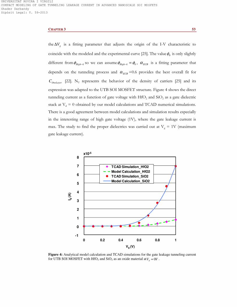
CHAPTER 3 53
theg
V∆ is a fitting parameter that adjusts the origin of the I-V characteristic to
coincide with the modeled and the experimental curve [25]. The value 0φ is only slightly
different fromHigh k
φ − so we can assume0High k
φ φ− = , ECBα is a fitting parameter that
depends on the tunneling process and ECBα =0.6 provides the best overall fit for
OneLayerC [22]. NT represents the behavior of the density of carriers [25] and its
expression was adapted to the UTB SOI MOSFET structure. Figure 4 shows the direct
tunneling current as a function of gate voltage with HfO2 and SiO2 as a gate dielectric
stack at Vd = 0 obtained by our model calculations and TCAD numerical simulations.
There is a good agreement between model calculations and simulation results especially
in the interesting range of high gate voltage (1V), where the gate leakage current is
max. The study to find the proper dielectrics was carried out at Vg = 1V (maximum
gate leakage current).
0 0.2 0.4 0.6 0.8 1
I g(A
)
Vg (V)
TCAD Simulation_HfO2
Model Calculation_HfO2
TCAD Simulation_SiO2
Model Calculation_SiO2
-1
2
3
4
5
7
8
6
1
0
x10-5
Figure 4: Analytical model calculation and TCAD simulations for the gate leakage tunneling current
for UTB SOI MOSFET with HfO2 and SiO2 as an oxide material at 0dV V= .
UNIVERSITAT ROVIRA I VIRGILI COMPACT MODELING OF GATE TUNNELING LEAKAGE CURRENT IN ADVANCED NANOSCALE SOI MOSFETS Ghader Darbandy Dipòsit Legal: T. 59-2013
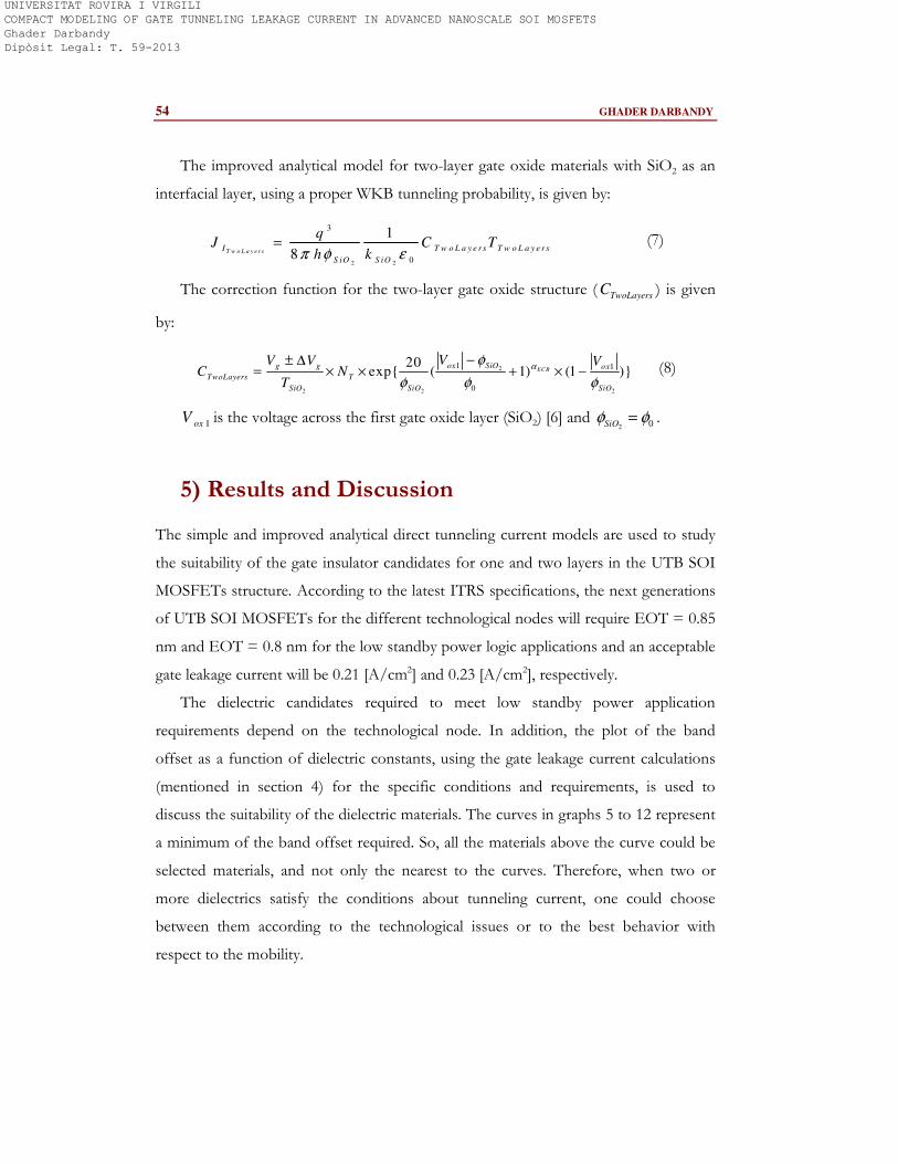
54 GHADER DARBANDY
The improved analytical model for two-layer gate oxide materials with SiO2 as an
interfacial layer, using a proper WKB tunneling probability, is given by:
2 2
3
0
1
8T w o L a y e r sI T w o L a y e r s T w o L a y e r s
S iO S iO
qJ C T
h kπ φ ε= (7)
The correction function for the two-layer gate oxide structure (TwoLayers
C ) is given
by:
2
2 2 2
1 1
0
20exp{ ( 1) (1 )}ECB
ox SiOg g ox
TwoLayers T
SiO SiO SiO
VV V VC N
T
αφ
φ φ φ
−± ∆= × × + × − (8)
1oxV is the voltage across the first gate oxide layer (SiO2) [6] and 2 0SiO
φ φ= .
5) Results and Discussion
The simple and improved analytical direct tunneling current models are used to study
the suitability of the gate insulator candidates for one and two layers in the UTB SOI
MOSFETs structure. According to the latest ITRS specifications, the next generations
of UTB SOI MOSFETs for the different technological nodes will require EOT = 0.85
nm and EOT = 0.8 nm for the low standby power logic applications and an acceptable
gate leakage current will be 0.21 [A/cm2] and 0.23 [A/cm2], respectively.
The dielectric candidates required to meet low standby power application
requirements depend on the technological node. In addition, the plot of the band
offset as a function of dielectric constants, using the gate leakage current calculations
(mentioned in section 4) for the specific conditions and requirements, is used to
discuss the suitability of the dielectric materials. The curves in graphs 5 to 12 represent
a minimum of the band offset required. So, all the materials above the curve could be
selected materials, and not only the nearest to the curves. Therefore, when two or
more dielectrics satisfy the conditions about tunneling current, one could choose
between them according to the technological issues or to the best behavior with
respect to the mobility.
UNIVERSITAT ROVIRA I VIRGILI COMPACT MODELING OF GATE TUNNELING LEAKAGE CURRENT IN ADVANCED NANOSCALE SOI MOSFETS Ghader Darbandy Dipòsit Legal: T. 59-2013
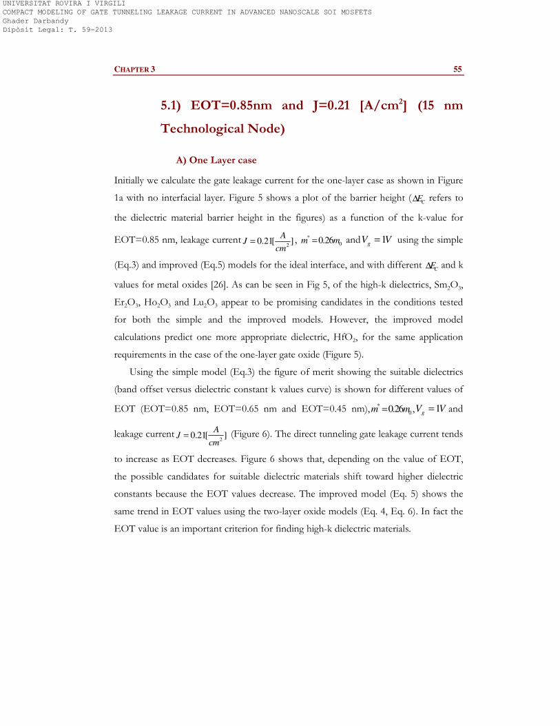
CHAPTER 3 55
5.1) EOT=0.85nm and J=0.21 [A/cm2] (15 nm
Technological Node)
A) One Layer case
Initially we calculate the gate leakage current for the one-layer case as shown in Figure
1a with no interfacial layer. Figure 5 shows a plot of the barrier height (C
E∆ refers to
the dielectric material barrier height in the figures) as a function of the k-value for
EOT=0.85 nm, leakage current2
0.21[ ]A
Jcm
= , *
00.26m m= and 1gV V= using the simple
(Eq.3) and improved (Eq.5) models for the ideal interface, and with different C
E∆ and k
values for metal oxides [26]. As can be seen in Fig 5, of the high-k dielectrics, Sm2O3,
Er2O3, Ho2O3 and Lu2O3 appear to be promising candidates in the conditions tested
for both the simple and the improved models. However, the improved model
calculations predict one more appropriate dielectric, HfO2, for the same application
requirements in the case of the one-layer gate oxide (Figure 5).
Using the simple model (Eq.3) the figure of merit showing the suitable dielectrics
(band offset versus dielectric constant k values curve) is shown for different values of
EOT (EOT=0.85 nm, EOT=0.65 nm and EOT=0.45 nm), *
00.26m m= , 1gV V= and
leakage current2
0.21[ ]A
Jcm
= (Figure 6). The direct tunneling gate leakage current tends
to increase as EOT decreases. Figure 6 shows that, depending on the value of EOT,
the possible candidates for suitable dielectric materials shift toward higher dielectric
constants because the EOT values decrease. The improved model (Eq. 5) shows the
same trend in EOT values using the two-layer oxide models (Eq. 4, Eq. 6). In fact the
EOT value is an important criterion for finding high-k dielectric materials.
UNIVERSITAT ROVIRA I VIRGILI COMPACT MODELING OF GATE TUNNELING LEAKAGE CURRENT IN ADVANCED NANOSCALE SOI MOSFETS Ghader Darbandy Dipòsit Legal: T. 59-2013
56 GHADER DARBANDY
La2O3
Ce2O3CeO2
Pr2O3(Amor)Pr2O3(Hex)
Sm2O3
Gd2O3
Ho2O3
Er2O3
Yb2O3
Lu2O3
HfO2
Y2O3
ZrO2
LaAlO3
LaScO3
ScO3
SiO2
0
0.5
1
1.5
2
2.5
3
3.5
4
4.5
0 10 20 30 40
Ba
nd
Off
se
t ∆
EC
(eV
)
Dielectric Constant k
EOT=0.85nm, m*=0.26m0Improved model
Selected materials
Simple model
Figure 5: Band offsetCE∆ as a function of the k-value for EOT=0.85 nm
with *
00.26m m= , 1gV V= and gate tunneling leakage current2
0.21[ ]A
Jcm
= using the simple and
improved models.
La2O3
Ce2O3
CeO2
Pr2O3(Amor)
Pr2O3(Hex)
Gd2O3
Ho2O3
Er2O3
Yb2O3
Lu2O3
HfO2
Y2O3
ZrO2
LaAlO3
La2CuO4
LiNbO3
LaScO3
ScO3
SiO2
0
0.5
1
1.5
2
2.5
3
3.5
4
4.5
0 10 20 30 40 50
Ba
nd
Off
se
t ∆
EC
(eV
)
Dielectric Constant k
EOT=0.85 EOT=0.65 EOT=0.45 Simple model, m*=0.26m0
Figure 6: Band offsetC
E∆ as a function of the k-value for EOT=0.85 nm, EOT=0.65 nm and
EOT=0.45 nm, *
00.26m m= , 1gV V= and gate tunneling leakage current2
0.21[ ]A
Jcm
= using the
simple model.
UNIVERSITAT ROVIRA I VIRGILI COMPACT MODELING OF GATE TUNNELING LEAKAGE CURRENT IN ADVANCED NANOSCALE SOI MOSFETS Ghader Darbandy Dipòsit Legal: T. 59-2013
CHAPTER 3 57
B) SiO2 as an Interfacial Layer
Eq.2 shows the exponential dependence of the tunneling probability in the two-layer
case on the interfacial layer thickness (2SiOT ); as a result the direct tunneling gate
leakage current (Eq. 4 and Eq. 7) also exponentially depends on2SiOT . We study the
suitability of high-k dielectric materials depending on the interfacial layer thickness.
Figure 7 shows the band offset as a function of the k-value for EOT=0.85 nm with
two different interfacial layer thicknesses (2
0.35SiOT nm= and2
0.55SiOT nm= ) using the
simple (Eq. 4) and improved (Eq. 7) analytical gate leakage current models. We see in
Figure 7 that using the improved model (Eq. 7) with *
00.26m m= , 1gV V= and leakage
current2
0.21[ ]A
Jcm
= , of the high-k gate oxides, the best candidates near the minimum
of the band offset, are CeO2, ZrO2 and HfO2. By changing only the interfacial layer
(SiO2) thickness (assuming all other parameters are the same as before) to
20.55SiOT nm= the preferred high-k materials near the minimum of the band offset, are
Pr2O3 in the hexagonal phase, La2O3 and La2CuO4. In fact, the thickness of SiO2 (as an
interfacial layer) affects which candidates should be chosen to meet the technological
node requirements. The same trend is observed when the simple model is used with
different thicknesses of the interfacial layer (SiO2) to select suitable dielectrics (Figure
7).
The tunneling electron effective mass in dielectric materials changes with the oxide
thickness and voltage across the oxide materials [24] and the values reported in the
literature vary over a wide range [27, 28]. We have shown the role of electron effective
mass values and their effect on the determination of suitable dielectrics.
Figure 8 shows the band offset as a function of the k-value for two different values
of the tunneling electron effective mass, *
00.20m m= and *
00.60m m= (EOT=0.85 nm
with tSiO2=0.55 nm, 1gV V= and leakage current2
0.21[ ]A
Jcm
= ) using the simple (Eq.4)
and improved (Eq.7) gate leakage current models.
UNIVERSITAT ROVIRA I VIRGILI COMPACT MODELING OF GATE TUNNELING LEAKAGE CURRENT IN ADVANCED NANOSCALE SOI MOSFETS Ghader Darbandy Dipòsit Legal: T. 59-2013
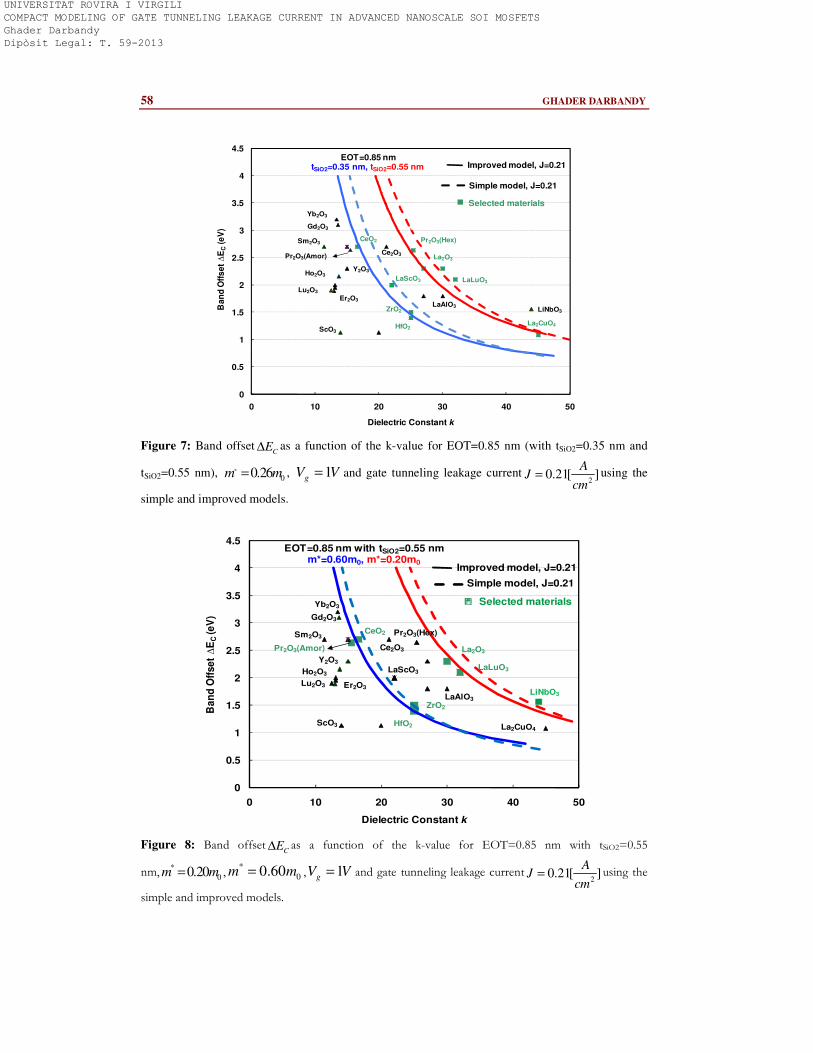
58 GHADER DARBANDY
La2O3
Ce2O3
CeO2
Pr2O3(Amor)
Pr2O3(Hex)Sm2O3
Gd2O3
Ho2O3
Er2O3
Yb2O3
Lu2O3
HfO2
Y2O3
ZrO2
LaAlO3
La2CuO4
LiNbO3
LaScO3
ScO3
LaLuO3
0
0.5
1
1.5
2
2.5
3
3.5
4
4.5
0 10 20 30 40 50
Ba
nd
Off
se
t ∆
EC
(eV
)
Dielectric Constant k
Improved model, J=0.21
Selected materials
EOT=0.85 nmtSiO2=0.35 nm, tSiO2=0.55 nm
Simple model, J=0.21
Figure 7: Band offsetC
E∆ as a function of the k-value for EOT=0.85 nm (with tSiO2=0.35 nm and
tSiO2=0.55 nm), *
00.26m m= , 1gV V= and gate tunneling leakage current2
0.21[ ]A
Jcm
= using the
simple and improved models.
La2O3Ce2O3
CeO2
Pr2O3(Amor)
Pr2O3(Hex)Sm2O3
Gd2O3
Ho2O3
Er2O3
Yb2O3
Lu2O3
HfO2
Y2O3
ZrO2
LaAlO3
La2CuO4
LiNbO3
LaScO3
ScO3
LaLuO3
0
0.5
1
1.5
2
2.5
3
3.5
4
4.5
0 10 20 30 40 50
Ba
nd
Off
se
t ∆
EC
(eV
)
Dielectric Constant k
Improved model, J=0.21
Selected materials
EOT=0.85 nm with tSiO2=0.55 nmm*=0.60m0, m*=0.20m0
Simple model, J=0.21
Figure 8: Band offsetCE∆ as a function of the k-value for EOT=0.85 nm with tSiO2=0.55
nm, *
00.20m m= ,*
00.60m m= , 1gV V= and gate tunneling leakage current2
0.21[ ]A
Jcm
= using the
simple and improved models.
UNIVERSITAT ROVIRA I VIRGILI COMPACT MODELING OF GATE TUNNELING LEAKAGE CURRENT IN ADVANCED NANOSCALE SOI MOSFETS Ghader Darbandy Dipòsit Legal: T. 59-2013
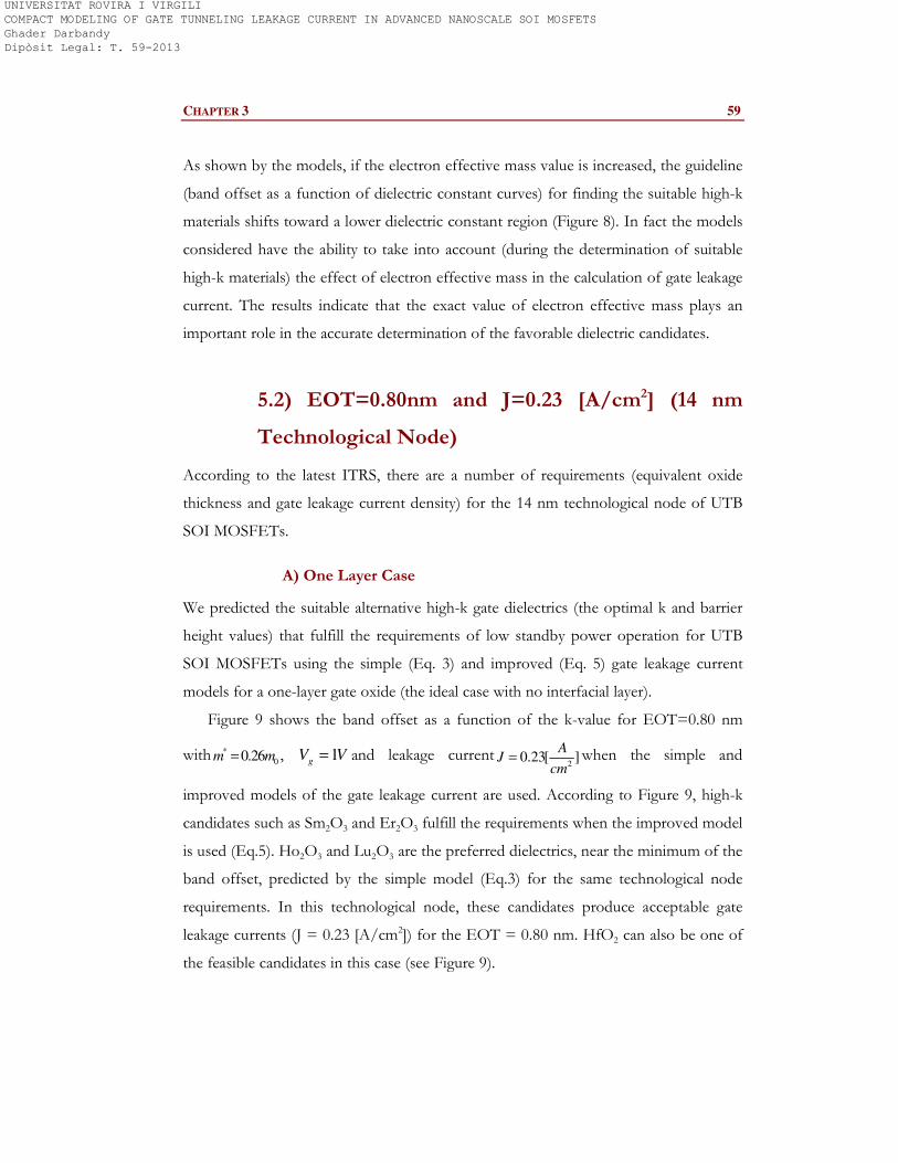
CHAPTER 3 59
As shown by the models, if the electron effective mass value is increased, the guideline
(band offset as a function of dielectric constant curves) for finding the suitable high-k
materials shifts toward a lower dielectric constant region (Figure 8). In fact the models
considered have the ability to take into account (during the determination of suitable
high-k materials) the effect of electron effective mass in the calculation of gate leakage
current. The results indicate that the exact value of electron effective mass plays an
important role in the accurate determination of the favorable dielectric candidates.
5.2) EOT=0.80nm and J=0.23 [A/cm2] (14 nm
Technological Node)
According to the latest ITRS, there are a number of requirements (equivalent oxide
thickness and gate leakage current density) for the 14 nm technological node of UTB
SOI MOSFETs.
A) One Layer Case
We predicted the suitable alternative high-k gate dielectrics (the optimal k and barrier
height values) that fulfill the requirements of low standby power operation for UTB
SOI MOSFETs using the simple (Eq. 3) and improved (Eq. 5) gate leakage current
models for a one-layer gate oxide (the ideal case with no interfacial layer).
Figure 9 shows the band offset as a function of the k-value for EOT=0.80 nm
with *
00.26m m= , 1gV V= and leakage current2
0.23[ ]A
Jcm
= when the simple and
improved models of the gate leakage current are used. According to Figure 9, high-k
candidates such as Sm2O3 and Er2O3 fulfill the requirements when the improved model
is used (Eq.5). Ho2O3 and Lu2O3 are the preferred dielectrics, near the minimum of the
band offset, predicted by the simple model (Eq.3) for the same technological node
requirements. In this technological node, these candidates produce acceptable gate
leakage currents (J = 0.23 [A/cm2]) for the EOT = 0.80 nm. HfO2 can also be one of
the feasible candidates in this case (see Figure 9).
UNIVERSITAT ROVIRA I VIRGILI COMPACT MODELING OF GATE TUNNELING LEAKAGE CURRENT IN ADVANCED NANOSCALE SOI MOSFETS Ghader Darbandy Dipòsit Legal: T. 59-2013
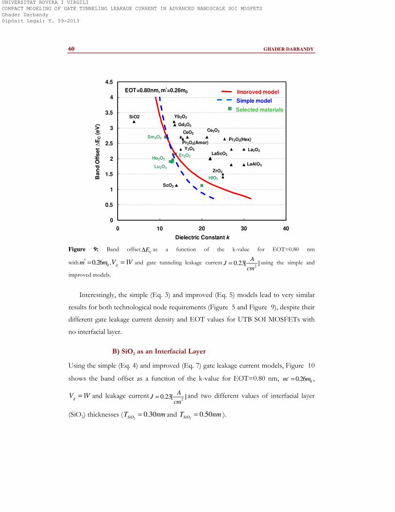
60 GHADER DARBANDY
La2O3
Ce2O3CeO2
Pr2O3(Amor)Pr2O3(Hex)
Sm2O3
Gd2O3
Ho2O3Er2O3
Yb2O3
Lu2O3
HfO2
Y2O3
ZrO2
LaAlO3
LaScO3
ScO3
SiO2
0
0.5
1
1.5
2
2.5
3
3.5
4
4.5
0 10 20 30 40
Ba
nd
Off
se
t ∆
EC
(eV
)
Dielectric Constant k
EOT=0.80nm, m*=0.26m0 Improved model
Selected materials
Simple model
Figure 9: Band offsetCE∆ as a function of the k-value for EOT=0.80 nm
with *
00.26m m= , 1gV V= and gate tunneling leakage current2
0.23[ ]A
Jcm
= using the simple and
improved models.
Interestingly, the simple (Eq. 3) and improved (Eq. 5) models lead to very similar
results for both technological node requirements (Figure 5 and Figure 9), despite their
different gate leakage current density and EOT values for UTB SOI MOSFETs with
no interfacial layer.
B) SiO2 as an Interfacial Layer
Using the simple (Eq. 4) and improved (Eq. 7) gate leakage current models, Figure 10
shows the band offset as a function of the k-value for EOT=0.80 nm, *
00.26m m= ,
1gV V= and leakage current2
0.23[ ]A
Jcm
= and two different values of interfacial layer
(SiO2) thicknesses (2
0.30SiOT nm= and 2
0.50SiOT nm= ).
UNIVERSITAT ROVIRA I VIRGILI COMPACT MODELING OF GATE TUNNELING LEAKAGE CURRENT IN ADVANCED NANOSCALE SOI MOSFETS Ghader Darbandy Dipòsit Legal: T. 59-2013
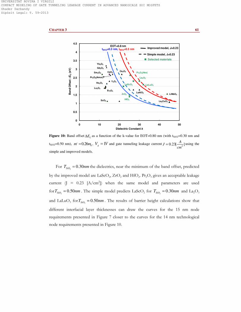
CHAPTER 3 61
La2O3
Ce2O3CeO2
Pr2O3(Amor)
Pr2O3(Hex)Sm2O3
Gd2O3
Ho2O3
Er2O3
Yb2O3
Lu2O3
HfO2
Y2O3
ZrO2
LaAlO3
La2CuO4
LiNbO3
LaScO3
ScO3
LaLuO3
0
0.5
1
1.5
2
2.5
3
3.5
4
4.5
0 10 20 30 40 50
Ba
nd
Off
se
t ∆
EC
(eV
)
Dielectric Constant k
Improved model, J=0.23
Selected materials
EOT=0.8 nmtSiO2=0.3 nm, tSiO2=0.5 nm
Simple model, J=0.23
Figure 10: Band offsetC
E∆ as a function of the k-value for EOT=0.80 nm (with tSiO2=0.30 nm and
tSiO2=0.50 nm), *
00.26m m= , 1gV V= and gate tunneling leakage current2
0.23[ ]A
Jcm
= using the
simple and improved models.
For 2
0.30SiOT nm= the dielectrics, near the minimum of the band offset, predicted
by the improved model are LaScO2, ZrO2 and HfO2. Pr2O3 gives an acceptable leakage
current (J = 0.23 [A/cm2]) when the same model and parameters are used
for2
0.50SiOT nm= . The simple model predicts LaScO2 for 2
0.30SiOT nm= and La2O3
and LaLuO3 for2
0.50SiOT nm= . The results of barrier height calculations show that
different interfacial layer thicknesses can draw the curves for the 15 nm node
requirements presented in Figure 7 closer to the curves for the 14 nm technological
node requirements presented in Figure 10.
UNIVERSITAT ROVIRA I VIRGILI COMPACT MODELING OF GATE TUNNELING LEAKAGE CURRENT IN ADVANCED NANOSCALE SOI MOSFETS Ghader Darbandy Dipòsit Legal: T. 59-2013
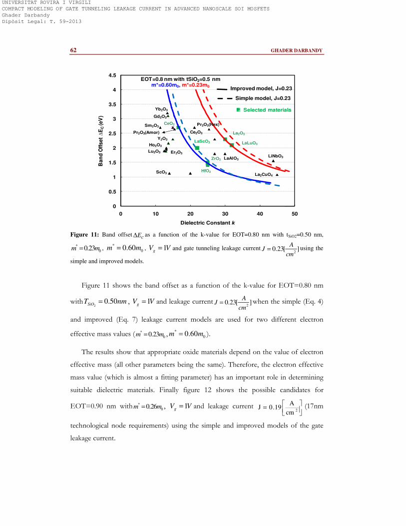
62 GHADER DARBANDY
La2O3Ce2O3
CeO2
Pr2O3(Amor)
Pr2O3(Hex)Sm2O3
Gd2O3
Ho2O3
Er2O3
Yb2O3
Lu2O3
HfO2
Y2O3
ZrO2 LaAlO3
La2CuO4
LiNbO3
LaScO3
ScO3
LaLuO3
0
0.5
1
1.5
2
2.5
3
3.5
4
4.5
0 10 20 30 40 50
Ba
nd
Off
se
t ∆
EC
(eV
)
Dielectric Constant k
Selected materials
EOT=0.8 nm with tSiO2=0.5 nmm*=0.60m0, m*=0.23m0
Simple model, J=0.23
Improved model, J=0.23
Figure 11: Band offsetC
E∆ as a function of the k-value for EOT=0.80 nm with tSiO2=0.50 nm,
*
00.23m m= , *
00.60m m= , 1gV V= and gate tunneling leakage current2
0.23[ ]A
Jcm
= using the
simple and improved models.
Figure 11 shows the band offset as a function of the k-value for EOT=0.80 nm
with2
0.50SiOT nm= , 1gV V= and leakage current2
0.23[ ]A
Jcm
= when the simple (Eq. 4)
and improved (Eq. 7) leakage current models are used for two different electron
effective mass values ( *
00.23m m= , *
00.60m m= ).
The results show that appropriate oxide materials depend on the value of electron
effective mass (all other parameters being the same). Therefore, the electron effective
mass value (which is almost a fitting parameter) has an important role in determining
suitable dielectric materials. Finally figure 12 shows the possible candidates for
EOT=0.90 nm with *
00.26m m= , 1gV V= and leakage current
=
2cm
A19.0J (17nm
technological node requirements) using the simple and improved models of the gate
leakage current.
UNIVERSITAT ROVIRA I VIRGILI COMPACT MODELING OF GATE TUNNELING LEAKAGE CURRENT IN ADVANCED NANOSCALE SOI MOSFETS Ghader Darbandy Dipòsit Legal: T. 59-2013
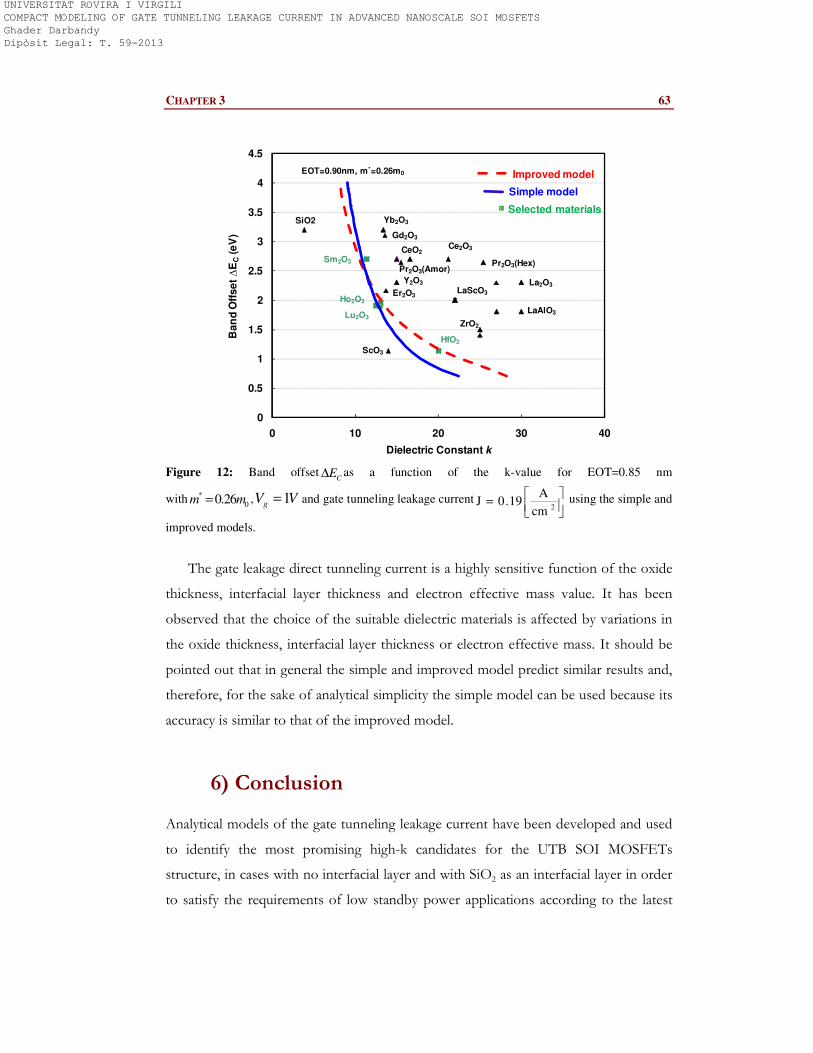
CHAPTER 3 63
La2O3
Ce2O3CeO2
Pr2O3(Amor)Pr2O3(Hex)Sm2O3
Gd2O3
Ho2O3
Er2O3
Yb2O3
Lu2O3
HfO2
Y2O3
ZrO2
LaAlO3
LaScO3
ScO3
SiO2
0
0.5
1
1.5
2
2.5
3
3.5
4
4.5
0 10 20 30 40
Ban
d O
ffse
t ∆
EC
(eV
)
Dielectric Constant k
EOT=0.90nm, m*=0.26m0 Improved model
Selected materials
Simple model
Figure 12: Band offsetC
E∆ as a function of the k-value for EOT=0.85 nm
with *
00.26m m= , 1gV V= and gate tunneling leakage current
=
2cm
A19.0J using the simple and
improved models.
The gate leakage direct tunneling current is a highly sensitive function of the oxide
thickness, interfacial layer thickness and electron effective mass value. It has been
observed that the choice of the suitable dielectric materials is affected by variations in
the oxide thickness, interfacial layer thickness or electron effective mass. It should be
pointed out that in general the simple and improved model predict similar results and,
therefore, for the sake of analytical simplicity the simple model can be used because its
accuracy is similar to that of the improved model.
6) Conclusion
Analytical models of the gate tunneling leakage current have been developed and used
to identify the most promising high-k candidates for the UTB SOI MOSFETs
structure, in cases with no interfacial layer and with SiO2 as an interfacial layer in order
to satisfy the requirements of low standby power applications according to the latest
UNIVERSITAT ROVIRA I VIRGILI COMPACT MODELING OF GATE TUNNELING LEAKAGE CURRENT IN ADVANCED NANOSCALE SOI MOSFETS Ghader Darbandy Dipòsit Legal: T. 59-2013
64 GHADER DARBANDY
ITRS roadmap. The suitability of the materials depends on the technology node
requirements and, particularly, EOT, the electron effective mass and interfacial layer
thickness can change the choice of the dielectric candidates. It has been found that
HfO2 and Lu2O3 are the most promising gate oxide materials for the 17nm, 15nm and
14nm technological node requirements assuming the ideal case with no interfacial
layer. This study provides additional insight into choosing the favorable dielectric
candidates for the different technological nodes in the future.
References
[1] Depas M, Vermeire B, Mertens P W, Van Meirhaeghe R L and Heyns M M,
“Determination of tunneling parameters in ultra-thin oxide layer poly-Si/SiO2/Si
structures” Solid-State Electron 38 (1995) 1465
[2] Lo S H, Buchanan D A, Taur Y and Wang W, “Quantum-mechanical modeling of
electron tunneling current from the inversion layer of ultra-thin-oxide nMOSFET’s”
IEEE Electron Dev.Lett., vol. 18, p. 209, 1997
[3] Merzbacher E 1998 Quantum Mechanics (New York: Wiley)
[4] Fromhold A T 1981 Quantum Mechanics for Applied Physics and Engineering
(New York: Dover)
[5] G. Darbandy, R. Ritzenthaler, F. Lime, I. Garduño, M. Estrada, A. Cerdeira and B.
Iñiguez, “Analytical Modeling of the Gate Tunneling Leakage for the Determination of
Adequate High-k Dielectrics in Double-Gate SOI MOSFETs at the 22 nm node”,
Solid-State Electronics, 54 (2010), pp. 1083-1087
[6] G. Darbandy, R. Ritzenthaler, F. Lime, I. Garduño, M. Estrada, A. Cerdeira and B.
Iñiguez, “Analytical Modeling of Direct Tunneling Current through SiO2/high-k Gate
Stacks for the Determination of Suitable High-k Dielectrics for Nanoscale Double-
Gate MOSFETs”, Semicond. Sci. Technol. 26 (2011) 045002
[7] M. Houssa, M. Tuominen, M. Naili, V. Afanas’ev, A. Stesmans, S. Haukka, M. M.
Heyns. “Trap-assisted tunneling in high permittivity gate dielectric stacks”. J Appl Phys
2000; 87(12):8615
UNIVERSITAT ROVIRA I VIRGILI COMPACT MODELING OF GATE TUNNELING LEAKAGE CURRENT IN ADVANCED NANOSCALE SOI MOSFETS Ghader Darbandy Dipòsit Legal: T. 59-2013
CHAPTER 3 65
[8] GD. Wilk, RM. Wallace, JM. Anthony. “High-k gate dielectrics: current status and
materials properties”. J. Appl. Phys., vol. 89, pp. 5243–5275, 2001
[9] A. Ghetti, E. Sangiorgi, J. Bude, T. W. Sorsch and G. Weber “Tunneling into
Interface States as Reliability Monitor for Ultrathin Oxides” IEEE Trans Electron Dev
47 (2000), pp. 2358–2365
[10] F. Lime, G. Ghibaudo and G. Guegan, “Stress induced leakage current at low field
in ultra thin oxides” Microelectronics Reliability, 41 (2001) 1421-1425
[11] Fischetti M. V., D. Neumayer and E. A. Cartier, "Effective Electron Mobility in Si
Inversion Layers in Metal-Oxide-Semiconductor Systems with A High-k Insulator: The
Role of Remote Phonon Scattering", Journal of Applied Physics, vol. 90, pp. 4587-
4608, November 2001
[12] B. Laikhtman and P. M. Solomon, “Remote phonon scattering in field effect
transistors with a high-k insulating layer” J. Appl. Phys, 103:014501, 2008
[13] J. P. Locquet, C. Marchiori, M. Sousa, J. Fompeyrine, "High-k dielectrics for the
gate stack", Journal of Applied Physics, 100, 051610 (2006)
[14] J. C. Ranuarez, M. J. Deen and C-H. Chen. “A review of gate tunneling current in
MOS devices”, Microelectronics Reliability 46 (2006) 1939-1956
[15] T. Kauerauf, B. Govoreanu, R. Degraeve, G. Groeseneken, H. Maes. “Finding the
gate stack with the lowest leakage current”, Solid State Electron 2005; 49(5):695–701
[16] F. Lime, R. Ritzenthaler, M. Ricona, F. Martinez, F. Pascal, E. Miranda, O. Faynot
and B. Iñiguez, “A Simplified Physically-Based DC Compact Model for Undoped UTB
SOI and Asymmetric DG MOSFETs with Independent Gate Operation”, Solid State
Electronics 57 (2011), pp. 61-66
[17]. J. Robertson, “Band offsets of wide-band-gap oxides and implications for future
electronic devices”, J. Vac. Sci. Technol. B 18, 1785 (2000)
[18] J. D. Plummer and P. B. Griffin, “Material and process limits in silicon VLSI
technology,” Proc. IEEE, vol. 89, pp. 240–258, Mar. 2001
[19] See the International Technology Roadmap for Semiconductors (ITRS 2009
Edition) at http://www.itrs.net
UNIVERSITAT ROVIRA I VIRGILI COMPACT MODELING OF GATE TUNNELING LEAKAGE CURRENT IN ADVANCED NANOSCALE SOI MOSFETS Ghader Darbandy Dipòsit Legal: T. 59-2013
66 GHADER DARBANDY
[20] K. F. Schuegraf and C. Hu, “Hole Injection SiO Breakdown model for very low
voltage lifetime extrapolation,” IEEE Trans. Electron Devices, vol. 41, no. 5, pp. 761–
767, 1994
[21] K. F. Schuegraf, C. C. King, and C. Hu, “Ultra-thin silicon dioxide leakage current
and scaling limit,” in: Symposium on VLSI Technology, Digest of Technical Papers,
1992, p. 18
[22] M. V. Dunga, X. Xi, J. He, I. Polishchuk, Q. Lu, M. Chan, A. M. Niknejad, and C.
Hu “Modeling of Direct Tunneling Current in Multi-Layer Gate Stacks”, in Proc of the
Workshop on Compact Modeling (WCM), Nanotech Conference, 2003, p. 306-309
[23] W-C. Lee, C. Hu. “Modeling CMOS tunneling currents through ultrathin gate
oxide due to conduction and valence-band electron and hole tunneling”. IEEE Trans
Electron Dev 2001; 48(7):1366-73
[24] R. Ludeke, E. Cartier, and A. Schenk, “Determination of the energy-dependent
conduction band mass in SiO2” Appl. Phys. Lett. 75, 1407 ~1999
[25] S. I. Garduño, A. Cerdeira M. Estrada, “Inclusion of Direct Tunneling Gate
Current in the Symmetric Doped Double Gate MOSFETs Model”, 2009 6th
International Conference on Electrical Engineering, Computing Science and Automatic Control
(CCE 2009). p. 675-678
[26] O. Engstrom, B. Raeissi, S. Hall, O. Buiu, M. C. Lemme, H. D. B. Gottlob, P.
Hurley and K. Cherkaoui, "Navigation aids in the search for future high-k dielectrics:
Physical and electrical trends", Solid State Electronics vol. 51, p. 622 (2007)
[27] Yee. Chia, Yeo, Tsu. Jae. King, Chenming. Hu, “MOSFET gate leakage modeling
and selection guide for alternative gate dielectrics based on leakage considerations”.
IEEE Trans. on ED, vol. 50, no. 4, April 2003, p. 1027-1035
[28] Francisco G. Ruiz · Andrés Godoy · Luca Donetti · I.M. Tienda-Luna ·Francisco
Gámiz · Carlos Sampedro “Accurate modeling of Metal/HfO2/Si capacitors”, J Comput
Electron 7:155–158 (2008)
UNIVERSITAT ROVIRA I VIRGILI COMPACT MODELING OF GATE TUNNELING LEAKAGE CURRENT IN ADVANCED NANOSCALE SOI MOSFETS Ghader Darbandy Dipòsit Legal: T. 59-2013
67
Chapter 4
Gate Leakage Current Partitioning in Nanoscale
Double-Gate MOSFETs, Using Compact Analytical
Model
This chapter presents a compact gate leakage current partitioning model for nanoscale
Double Gate (DG) MOSFETs, using analytical models of the direct tunneling gate
leakage current. Gate leakage current becomes important and an essential aspect of
MOSFET modeling as the gate oxide thickness is scaled down to 1nm and below in
advanced CMOS processes. We considered an ideal interface (ideal case without an
interfacial layer) and two layers high-k dielectric materials as gate insulators. In the case
of two layers, a thin layer of SiO2 as an interfacial layer is considered. The results of the
gate current partitioning components into drain and source show good agreement with
2D TCAD numerical device simulation (Silvaco ATLAS).
UNIVERSITAT ROVIRA I VIRGILI COMPACT MODELING OF GATE TUNNELING LEAKAGE CURRENT IN ADVANCED NANOSCALE SOI MOSFETS Ghader Darbandy Dipòsit Legal: T. 59-2013
68 GHADER DARBANDY
1) Introduction
The continuous reduction of the gate oxide layer thickness in advanced CMOS devices
to 1nm and below causes an increase of the gate leakage current density, due to the
increasing carrier direct tunneling and can become an important undesirable effect on
the device operation [1, 2]; besides, it increases power dissipation and can deteriorate
the device performance and circuit stability [3] for every process generation. Part of the
gate leakage current ( gcI ) is collected by the source ( gcsI ) while the rest goes to the
drain ( gcdI ). For an accurate characterization and modeling of the tunneling current
through high-k gate stacks and its effect on device and circuit performance, it is
essential to derive a compact model of the partition of the leakage current flowing
between gate and channel into the source (gcsI ) and drain (
gcdI ) components. Several
authors have studied and modeled the gate leakage current partition in single gate
MOSFET structures [4-6].
The main goal of the present chapter is to develop a compact analytical model of
the partitioning of the direct tunneling gate leakage current (gcI ) in nanoscale Double-
Gate (DG) MOSFETs. This model consists of analytical equations for the gate-source
and the gate-drain tunneling components. A gate leakage current model was developed
and implemented in our previous surface potential based model [7, 8] which includes
short channel effects related to the DG MOSFET structure. We considered an ideal
case, with one layer gate insulator, and also the case of a two-layer dielectric stack with
a thin layer of SiO2 (in order to maintain a good interface with substrate) as an
interfacial layer with a suitable gate oxide material (HfO2) are being proposed [9, 10].
In this chapter, in order to derive the gate-source ( gcsI ) and gate-drain ( gcdI )
leakage current components, current continuity equation is considered in the presence
of gate leakage current as a perturbation for a DG MOSFET at the voltage along the
channel as a function of x, which is 0 at the source and L (channel length) at the drain.
In fact the main goal of partition modeling is to solve the current continuity equation
for the channel current in the presence of the gate leakage. The model is therefore
UNIVERSITAT ROVIRA I VIRGILI COMPACT MODELING OF GATE TUNNELING LEAKAGE CURRENT IN ADVANCED NANOSCALE SOI MOSFETS Ghader Darbandy Dipòsit Legal: T. 59-2013
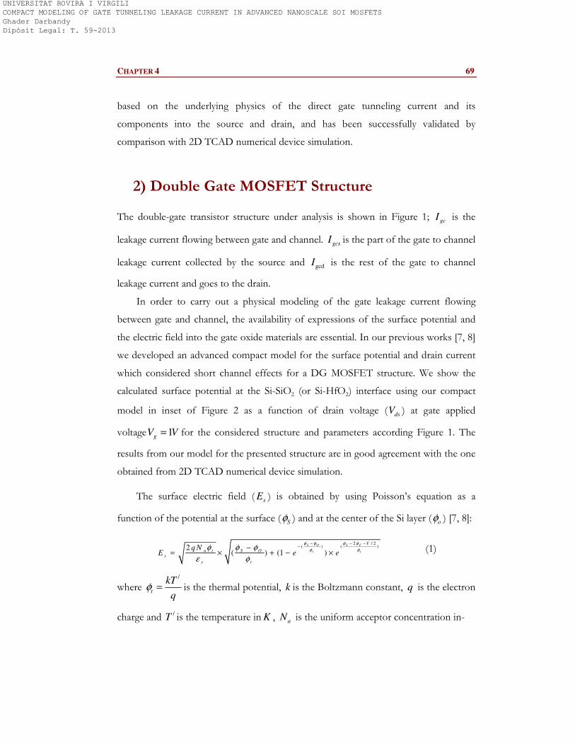
CHAPTER 4 69
based on the underlying physics of the direct gate tunneling current and its
components into the source and drain, and has been successfully validated by
comparison with 2D TCAD numerical device simulation.
2) Double Gate MOSFET Structure
The double-gate transistor structure under analysis is shown in Figure 1; gcI is the
leakage current flowing between gate and channel. gcsI is the part of the gate to channel
leakage current collected by the source and gcdI is the rest of the gate to channel
leakage current and goes to the drain.
In order to carry out a physical modeling of the gate leakage current flowing
between gate and channel, the availability of expressions of the surface potential and
the electric field into the gate oxide materials are essential. In our previous works [7, 8]
we developed an advanced compact model for the surface potential and drain current
which considered short channel effects for a DG MOSFET structure. We show the
calculated surface potential at the Si-SiO2 (or Si-HfO2) interface using our compact
model in inset of Figure 2 as a function of drain voltage ( dsV ) at gate applied
voltage 1gV V= for the considered structure and parameters according Figure 1. The
results from our model for the presented structure are in good agreement with the one
obtained from 2D TCAD numerical device simulation.
The surface electric field ( sE ) is obtained by using Poisson’s equation as a
function of the potential at the surface ( Sφ ) and at the center of the Si layer ( oφ ) [7, 8]:
2 / 2( ) ( )2
( ) (1 )
S O S F
t t
V
a t S O
s
s t
q NE e e
φ φ φ φ
φ φφ φ φ
ε φ
− − −−−
= × + − × (1)
where /
t
kT
qφ = is the thermal potential, k is the Boltzmann constant, q is the electron
charge and /T is the temperature in K , aN is the uniform acceptor concentration in-
UNIVERSITAT ROVIRA I VIRGILI COMPACT MODELING OF GATE TUNNELING LEAKAGE CURRENT IN ADVANCED NANOSCALE SOI MOSFETS Ghader Darbandy Dipòsit Legal: T. 59-2013
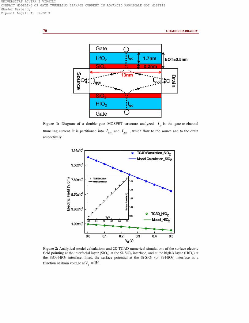
70 GHADER DARBANDY
EOT=0.5nm
So
urc
e
Dra
inIgcsIgcd
Igc
HfO2
HfO2
SiO2
SiO2
Gate
Gate
0.2nm
1.7nm
13nm
Igc
Figure 1: Diagram of a double gate MOSFET structure analyzed. gcI is the gate-to-channel
tunneling current. It is partitioned into gcsI and gcdI , which flow to the source and to the drain
respectively.
0.0 0.1 0.2 0.3 0.4 0.5
1.90x10⁶
3.80x10⁶
5.70x10⁶
7.60x10⁶
9.50x10⁶
1.14x10⁷
0.0 0.1 0.2 0.3 0.4 0.5
0.95
1.00
1.05
1.10
1.15
Sur
face
Pot
entia
l (V)
Vd (V)
TCAD Simulation
Model Calculation
Vd (V)
TCAD Simulation_SiO2
Model Calculation_SiO2
Ele
ctr
ic F
ield
(V
/cm
)
TCAD_HfO2
Model_HfO2
Figure 2: Analytical model calculations and 2D TCAD numerical simulations of the surface electric
field pointing at the interfacial layer (SiO2) at the Si-SiO2 interface, and at the high-k layer (HfO2) at
the SiO2-HfO2 interface, Inset: the surface potential at the Si-SiO2 (or Si-HfO2) interface as a
function of drain voltage at 1gV V= .
UNIVERSITAT ROVIRA I VIRGILI COMPACT MODELING OF GATE TUNNELING LEAKAGE CURRENT IN ADVANCED NANOSCALE SOI MOSFETS Ghader Darbandy Dipòsit Legal: T. 59-2013
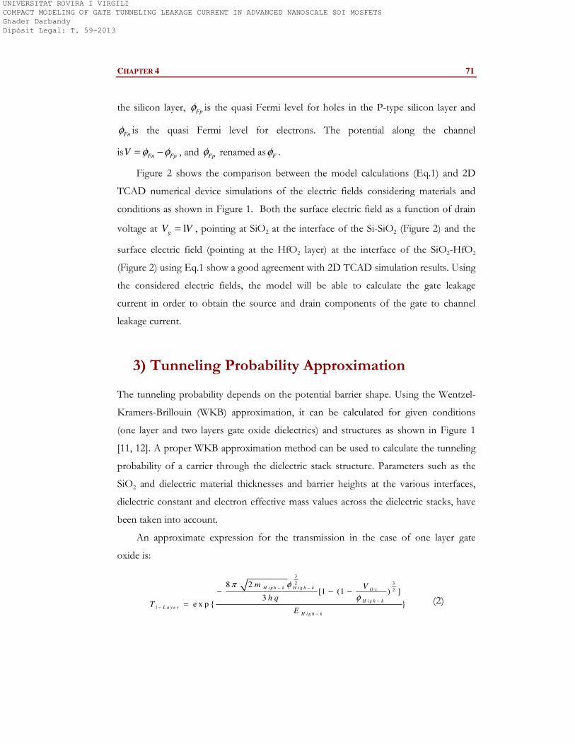
CHAPTER 4 71
the silicon layer, Fpφ is the quasi Fermi level for holes in the P-type silicon layer and
Fnφ is the quasi Fermi level for electrons. The potential along the channel
is Fn FpV φ φ= − , and Fpφ renamed as Fφ .
Figure 2 shows the comparison between the model calculations (Eq.1) and 2D
TCAD numerical device simulations of the electric fields considering materials and
conditions as shown in Figure 1. Both the surface electric field as a function of drain
voltage at 1gV V= , pointing at SiO2 at the interface of the Si-SiO2 (Figure 2) and the
surface electric field (pointing at the HfO2 layer) at the interface of the SiO2-HfO2
(Figure 2) using Eq.1 show a good agreement with 2D TCAD simulation results. Using
the considered electric fields, the model will be able to calculate the gate leakage
current in order to obtain the source and drain components of the gate to channel
leakage current.
3) Tunneling Probability Approximation
The tunneling probability depends on the potential barrier shape. Using the Wentzel-
Kramers-Brillouin (WKB) approximation, it can be calculated for given conditions
(one layer and two layers gate oxide dielectrics) and structures as shown in Figure 1
[11, 12]. A proper WKB approximation method can be used to calculate the tunneling
probability of a carrier through the dielectric stack structure. Parameters such as the
SiO2 and dielectric material thicknesses and barrier heights at the various interfaces,
dielectric constant and electron effective mass values across the dielectric stacks, have
been taken into account.
An approximate expression for the transmission in the case of one layer gate
oxide is:
3
2 3
2
1
8 2[1 (1 ) ]
3e x p { }
H i g h k H i g h k O x
H ig h k
L a y e r
H i g h k
m V
h qT
E
π φ
φ
− −
−
−
−
− − −
= (2)
UNIVERSITAT ROVIRA I VIRGILI COMPACT MODELING OF GATE TUNNELING LEAKAGE CURRENT IN ADVANCED NANOSCALE SOI MOSFETS Ghader Darbandy Dipòsit Legal: T. 59-2013
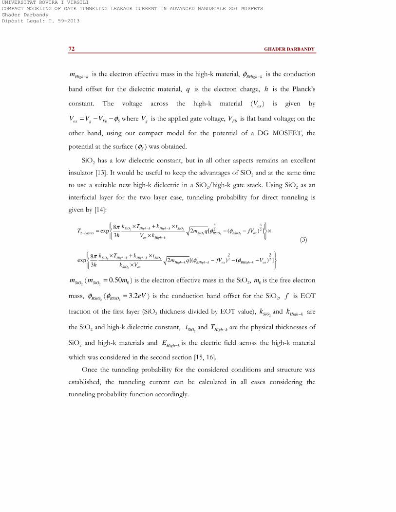
72 GHADER DARBANDY
High km − is the electron effective mass in the high-k material, BHigh kφ − is the conduction
band offset for the dielectric material, q is the electron charge, h is the Planck’s
constant. The voltage across the high-k material ( oxV ) is given by
ox g Fb SV V V φ= − − where gV is the applied gate voltage, FbV is flat band voltage; on the
other hand, using our compact model for the potential of a DG MOSFET, the
potential at the surface ( Sφ ) was obtained.
SiO2 has a low dielectric constant, but in all other aspects remains an excellent
insulator [13]. It would be useful to keep the advantages of SiO2 and at the same time
to use a suitable new high-k dielectric in a SiO2/high-k gate stack. Using SiO2 as an
interfacial layer for the two layer case, tunneling probability for direct tunneling is
given by [14]:
2 2
2 2 2
2 2
2
3 3
2 22
3 3
2 2
8exp 2 [ ( ) ]
3
8exp 2 [( ) ( ) ]
3
− −
−
−
− −
− − −
× + × = − − ×
×
× + × − − −
×
SiO High k High k SiO
Layers SiO BSiO BSiO ox
ox High k
SiO High k High k SiO
High k BHigh k ox BHigh k ox
SiO ox
k T k tT m q fV
h V k
k T k tm q fV V
h k V
πφ φ
πφ φ
(3)
2SiOm (2 00.50SiOm m= ) is the electron effective mass in the SiO2, 0m is the free electron
mass, 2BSiOφ (
23.2BSiO eVφ = ) is the conduction band offset for the SiO2, f is EOT
fraction of the first layer (SiO2 thickness divided by EOT value), 2SiOk and High kk − are
the SiO2 and high-k dielectric constant, 2SiOt and High kT − are the physical thicknesses of
SiO2 and high-k materials and High kE − is the electric field across the high-k material
which was considered in the second section [15, 16].
Once the tunneling probability for the considered conditions and structure was
established, the tunneling current can be calculated in all cases considering the
tunneling probability function accordingly.
UNIVERSITAT ROVIRA I VIRGILI COMPACT MODELING OF GATE TUNNELING LEAKAGE CURRENT IN ADVANCED NANOSCALE SOI MOSFETS Ghader Darbandy Dipòsit Legal: T. 59-2013
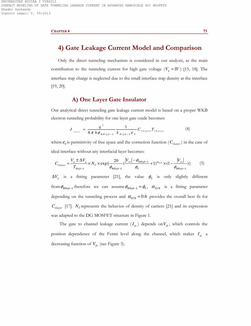
CHAPTER 4 73
4) Gate Leakage Current Model and Comparison
Only the direct tunneling mechanism is considered in our analysis, as the main
contribution to the tunneling current for high gate voltage ( 1gV V= ) [15, 18]. The
interface trap charge is neglected due to the small interface trap density at the interface
[19, 20].
A) One Layer Gate Insulator
Our analytical direct tunneling gate leakage current model is based on a proper WKB
electron tunneling probability for one layer gate oxide becomes:
1
3
1 1
0
1
8L a y e r L a y e r L a y e r
B H i g h k H i g h k
qJ C T
h kπ φ ε− −
= (4)
where 0ε is permittivity of free space and the correction function ( 1LayerC ) in the case of
ideal interface without any interfacial layer becomes:
1
0
20exp{ ( 1) (1 )}ECB
g g ox BHigh k ox
Layer T
High k BHigh k BHigh k
V V V VC N
T
αφ
φ φ φ
−
− − −
± ∆ −= × × + × − (5)
gV∆ is a fitting parameter [21], the value 0φ is only slightly different
from BHigh kφ − therefore we can assume 0BHigh kφ φ− ≈ , ECBα is a fitting parameter
depending on the tunneling process and 0.6ECBα = provides the overall best fit for
1LayerC [17]. TN represents the behavior of density of carriers [21] and its expression
was adapted to the DG MOSFET structure in Figure 1.
The gate to channel leakage current ( gcI ) depends on dsV , which controls the
position dependence of the Fermi level along the channel, which makes gcI a
decreasing function of dsV (see Figure 3).
UNIVERSITAT ROVIRA I VIRGILI COMPACT MODELING OF GATE TUNNELING LEAKAGE CURRENT IN ADVANCED NANOSCALE SOI MOSFETS Ghader Darbandy Dipòsit Legal: T. 59-2013
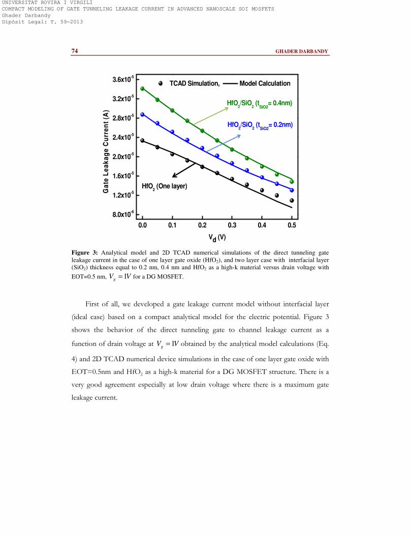
74 GHADER DARBANDY
0.0 0.1 0.2 0.3 0.4 0.5
8.0x10⁻⁶
1.2x10⁻⁵
1.6x10⁻⁵
2.0x10⁻⁵
2.4x10⁻⁵
2.8x10⁻⁵
3.2x10⁻⁵
3.6x10⁻⁵
HfO2 (One layer)
HfO2/SiO
2 (t
SiO2= 0.2nm)
HfO2/SiO
2 (t
SiO2= 0.4nm)
TCAD Simulation, Model Calculation
Ga
te L
ea
ka
ge
Cu
rre
nt
(A)
Vd (V)
Figure 3: Analytical model and 2D TCAD numerical simulations of the direct tunneling gate
leakage current in the case of one layer gate oxide (HfO2), and two layer case with interfacial layer
(SiO2) thickness equal to 0.2 nm, 0.4 nm and HfO2 as a high-k material versus drain voltage with
EOT=0.5 nm, 1gV V= for a DG MOSFET.
First of all, we developed a gate leakage current model without interfacial layer
(ideal case) based on a compact analytical model for the electric potential. Figure 3
shows the behavior of the direct tunneling gate to channel leakage current as a
function of drain voltage at 1gV V= obtained by the analytical model calculations (Eq.
4) and 2D TCAD numerical device simulations in the case of one layer gate oxide with
EOT=0.5nm and HfO2 as a high-k material for a DG MOSFET structure. There is a
very good agreement especially at low drain voltage where there is a maximum gate
leakage current.
UNIVERSITAT ROVIRA I VIRGILI COMPACT MODELING OF GATE TUNNELING LEAKAGE CURRENT IN ADVANCED NANOSCALE SOI MOSFETS Ghader Darbandy Dipòsit Legal: T. 59-2013
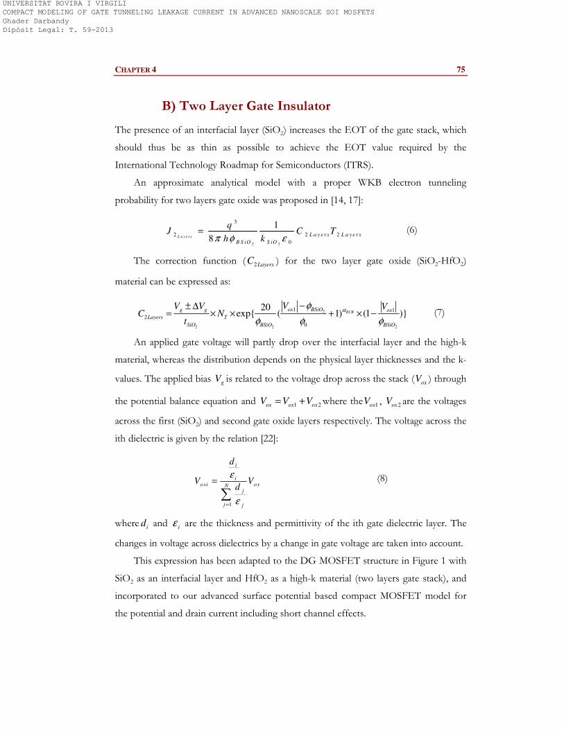
CHAPTER 4 75
B) Two Layer Gate Insulator
The presence of an interfacial layer (SiO2) increases the EOT of the gate stack, which
should thus be as thin as possible to achieve the EOT value required by the
International Technology Roadmap for Semiconductors (ITRS).
An approximate analytical model with a proper WKB electron tunneling
probability for two layers gate oxide was proposed in [14, 17]:
2 2
3
2 2 2
0
1
8L a y e r s L a y e r s L a y e r s
B S iO S iO
qJ C T
h kπ φ ε= (6)
The correction function ( 2LayersC ) for the two layer gate oxide (SiO2-HfO2)
material can be expressed as:
2
2 2 2
1 1
2
0
20exp{ ( 1) (1 )}
−± ∆= × × + × −ECB
ox BSiOg g ox
Layers T
SiO BSiO BSiO
VV V VC N
t
αφ
φ φ φ (7)
An applied gate voltage will partly drop over the interfacial layer and the high-k
material, whereas the distribution depends on the physical layer thicknesses and the k-
values. The applied bias gV is related to the voltage drop across the stack ( oxV ) through
the potential balance equation and 1 2ox ox oxV V V= + where the 1oxV , 2oxV are the voltages
across the first (SiO2) and second gate oxide layers respectively. The voltage across the
ith dielectric is given by the relation [22]:
1
i
ioxi oxN
j
j j
d
V Vd
ε
ε=
=
∑ (8)
where id and iε are the thickness and permittivity of the ith gate dielectric layer. The
changes in voltage across dielectrics by a change in gate voltage are taken into account.
This expression has been adapted to the DG MOSFET structure in Figure 1 with
SiO2 as an interfacial layer and HfO2 as a high-k material (two layers gate stack), and
incorporated to our advanced surface potential based compact MOSFET model for
the potential and drain current including short channel effects.
UNIVERSITAT ROVIRA I VIRGILI COMPACT MODELING OF GATE TUNNELING LEAKAGE CURRENT IN ADVANCED NANOSCALE SOI MOSFETS Ghader Darbandy Dipòsit Legal: T. 59-2013
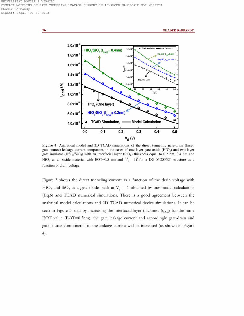
76 GHADER DARBANDY
0.0 0.1 0.2 0.3 0.4 0.5
4.0x10⁻⁶
6.0x10⁻⁶
8.0x10⁻⁶
1.0x10⁻⁵
1.2x10⁻⁵
1.4x10⁻⁵
1.6x10⁻⁵
1.8x10⁻⁵
2.0x10⁻⁵
0.0 0.1 0.2 0.3 0.4 0.5
5.00x10⁻⁶
7.50x10⁻⁶
1.00x10⁻⁵
1.25x10⁻⁵
1.50x10⁻⁵
1.75x10⁻⁵
HfO2 (One Layer)
TCAD Simulation, Model Calculation
I gc
s (
A)
Vd (V)
HfO2/SiO
2 (t
SiO2= 0.2nm)
HfO2/SiO
2 (t
SiO2= 0.4nm)
HfO2 (One layer)
TCAD Simulation, Model Calculation
I gc
d (
A)
Vd (V)
HfO2/SiO
2 (t
SiO2= 0.2nm)
HfO2/SiO
2 (t
SiO2= 0.4nm)
Figure 4: Analytical model and 2D TCAD simulations of the direct tunneling gate-drain (Inset:
gate-source) leakage current component, in the cases of one layer gate oxide (HfO2) and two layer
gate insulator (HfO2/SiO2) with an interfacial layer (SiO2) thickness equal to 0.2 nm, 0.4 nm and
HfO2 as an oxide material with EOT=0.5 nm and 1gV V= for a DG MOSFET structure as a
function of drain voltage.
Figure 3 shows the direct tunneling current as a function of the drain voltage with
HfO2 and SiO2 as a gate oxide stack at Vg = 1 obtained by our model calculations
(Eq.6) and TCAD numerical simulations. There is a good agreement between the
analytical model calculations and 2D TCAD numerical device simulations. It can be
seen in Figure 3, that by increasing the interfacial layer thickness (tSiO2) for the same
EOT value (EOT=0.5nm), the gate leakage current and accordingly gate-drain and
gate-source components of the leakage current will be increased (as shown in Figure
4).
UNIVERSITAT ROVIRA I VIRGILI COMPACT MODELING OF GATE TUNNELING LEAKAGE CURRENT IN ADVANCED NANOSCALE SOI MOSFETS Ghader Darbandy Dipòsit Legal: T. 59-2013
CHAPTER 4 77
5) Gate Leakage Partition Model and Validation
In this section, the gate leakage partition model based on the considered analytical gate
leakage current models for the one and two layer gate insulators is developed and
analyzed for a DG MOSFET structure. In order to obtain the gate current partition,
current continuity equation in the presence of the gate leakage current is necessary to
solve.
We have adapted to a DG MOSFET structure the gate leakage model with
source-drain partitioning that was derived for single gate MOSFET [4]. Using the drift
equation, the drain current for a DG MOSFET structure is given by:
2 ( )x ox gs th
dVI C V V V
dxµ= − − (9)
The current continuity equation for DG MOSFET structure is introduced:
( )( )
2 0g th
g
ox
dVd V V V
J xdx
dx Cµ
− − × + = (10)
thV is the threshold voltage, V is the channel potential reference to the source, µ is the
mobility, oxC is the oxide capacitance and ( )gJ x is the gate current density as a
function of channel location.
The current continuity equation assumed for DG MOSFET is solved without gate
leakage current ( ( ) 0gJ x = ). This assumption leads to exactly the same condition and
results of single gate MOSFET:
2
0 ( ) ( ) 2( ) ( )2 2 ( )
ds ds dsg th g th g th ds g th
g th
V V Vx xV x V V V V V V V V V
L V V L= − − − − − − ≈ − −
− (11)
where 0 ( )V x is the solution of Eq. (10) without gate leakage current.
The inclusion of the gate leakage current causes the change of channel potential
along the channel 0 1( ) ( ) ( )V x V x V x= + , assuming the gate leakage current is much
smaller than the drain current, the gate leakage current perturbation on ( )V x is small
UNIVERSITAT ROVIRA I VIRGILI COMPACT MODELING OF GATE TUNNELING LEAKAGE CURRENT IN ADVANCED NANOSCALE SOI MOSFETS Ghader Darbandy Dipòsit Legal: T. 59-2013
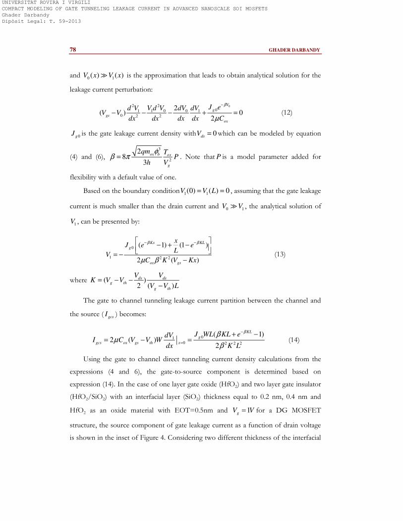
78 GHADER DARBANDY
and 0 1( ) ( )V x V x� is the approximation that leads to obtain analytical solution for the
leakage current perturbation:
02201 0 01 1
0 2 2
2( ) 0
2
V
g
gs
ox
J eV d V dVd V dVV V
dx dx dx dx C
β
µ
−
− − − + = (12)
0gJ is the gate leakage current density with 0dsV = which can be modeled by equation
(4) and (6), 3
2
28
3
ox b ox
g
qm TP
h V
φβ π= . Note that P is a model parameter added for
flexibility with a default value of one.
Based on the boundary condition 1 1(0) ( ) 0V V L= = , assuming that the gate leakage
current is much smaller than the drain current and 0 1V V� , the analytical solution of
1V , can be presented by:
0
1 2 2
( 1) (1 )
2 ( )
Kx KL
g
ox gs
xJ e e
LV
C K V Kx
β β
µ β
− − − + − = −
− (13)
where ( )2 ( )
ds dsg th
g th
V VK V V
V V L= − −
−
The gate to channel tunneling leakage current partition between the channel and
the source (gcsI ) becomes:
010 2 2 2
( 1)2 ( )
2
−
=
+ −= − =
KL
g
gcs ox gs th x
J WL KL edVI C V V W
dx K L
ββµ
β (14)
Using the gate to channel direct tunneling current density calculations from the
expressions (4 and 6), the gate-to-source component is determined based on
expression (14). In the case of one layer gate oxide (HfO2) and two layer gate insulator
(HfO2/SiO2) with an interfacial layer (SiO2) thickness equal to 0.2 nm, 0.4 nm and
HfO2 as an oxide material with EOT=0.5nm and 1gV V= for a DG MOSFET
structure, the source component of gate leakage current as a function of drain voltage
is shown in the inset of Figure 4. Considering two different thickness of the interfacial
UNIVERSITAT ROVIRA I VIRGILI COMPACT MODELING OF GATE TUNNELING LEAKAGE CURRENT IN ADVANCED NANOSCALE SOI MOSFETS Ghader Darbandy Dipòsit Legal: T. 59-2013
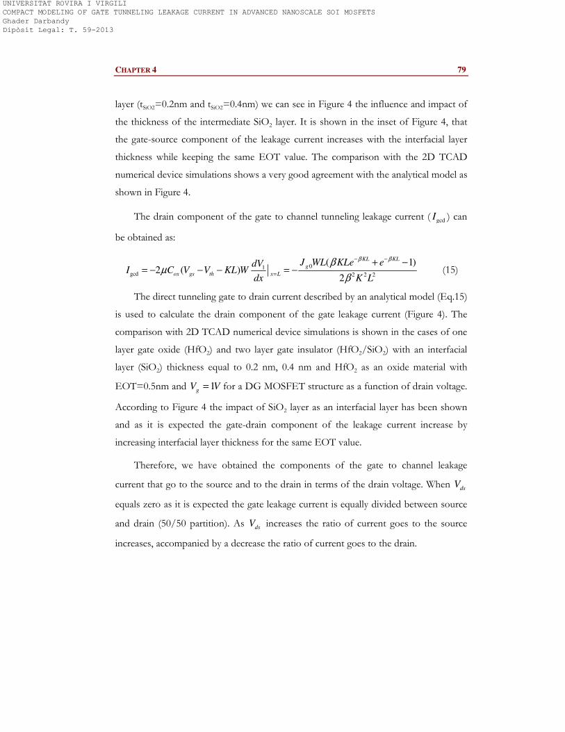
CHAPTER 4 79
layer (tSiO2=0.2nm and tSiO2=0.4nm) we can see in Figure 4 the influence and impact of
the thickness of the intermediate SiO2 layer. It is shown in the inset of Figure 4, that
the gate-source component of the leakage current increases with the interfacial layer
thickness while keeping the same EOT value. The comparison with the 2D TCAD
numerical device simulations shows a very good agreement with the analytical model as
shown in Figure 4.
The drain component of the gate to channel tunneling leakage current ( gcdI ) can
be obtained as:
01gcd 2 2 2
( 1)2 ( )
2
− −
=
+ −= − − − = −
KL KL
g
ox gs th x L
J WL KLe edVI C V V KL W
dx K L
β ββµ
β (15)
The direct tunneling gate to drain current described by an analytical model (Eq.15)
is used to calculate the drain component of the gate leakage current (Figure 4). The
comparison with 2D TCAD numerical device simulations is shown in the cases of one
layer gate oxide (HfO2) and two layer gate insulator (HfO2/SiO2) with an interfacial
layer (SiO2) thickness equal to 0.2 nm, 0.4 nm and HfO2 as an oxide material with
EOT=0.5nm and 1gV V= for a DG MOSFET structure as a function of drain voltage.
According to Figure 4 the impact of SiO2 layer as an interfacial layer has been shown
and as it is expected the gate-drain component of the leakage current increase by
increasing interfacial layer thickness for the same EOT value.
Therefore, we have obtained the components of the gate to channel leakage
current that go to the source and to the drain in terms of the drain voltage. When dsV
equals zero as it is expected the gate leakage current is equally divided between source
and drain (50/50 partition). As dsV increases the ratio of current goes to the source
increases, accompanied by a decrease the ratio of current goes to the drain.
UNIVERSITAT ROVIRA I VIRGILI COMPACT MODELING OF GATE TUNNELING LEAKAGE CURRENT IN ADVANCED NANOSCALE SOI MOSFETS Ghader Darbandy Dipòsit Legal: T. 59-2013
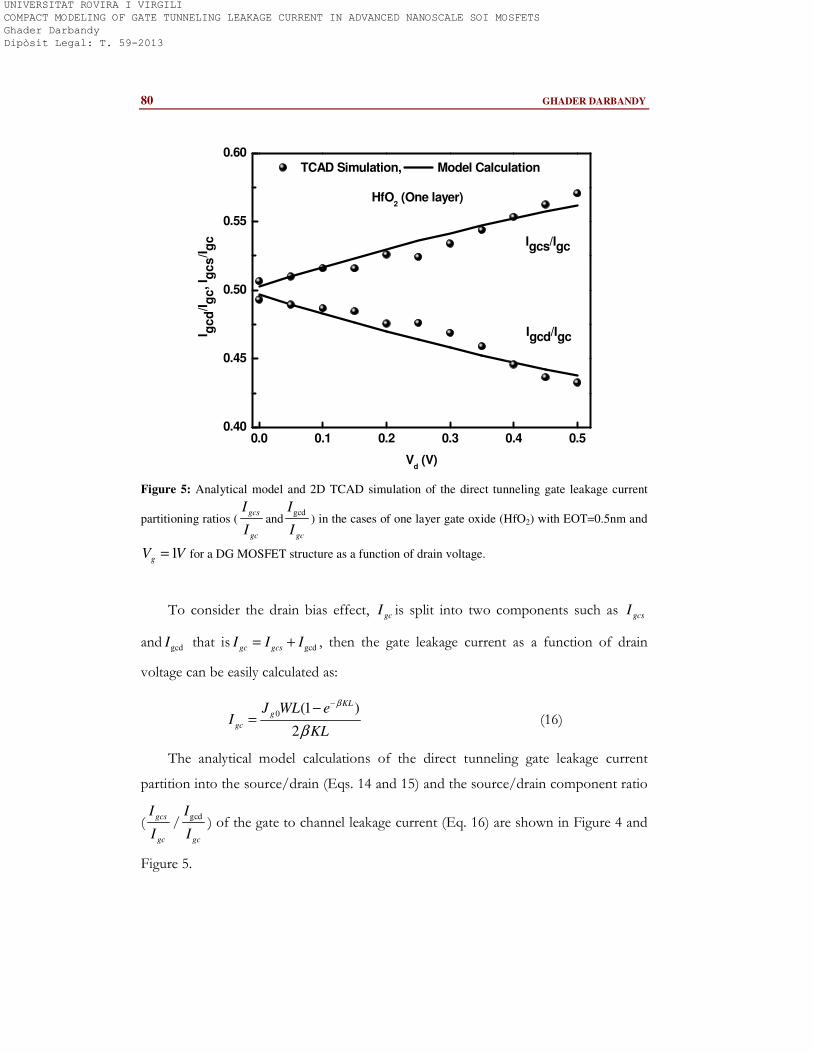
80 GHADER DARBANDY
0.0 0.1 0.2 0.3 0.4 0.50.40
0.45
0.50
0.55
0.60
HfO2 (One layer)
Igcd/Igc
I gc
d/Ig
c, I g
cs
/Ig
c
Vd (V)
TCAD Simulation, Model Calculation
Igcs/Igc
Figure 5: Analytical model and 2D TCAD simulation of the direct tunneling gate leakage current
partitioning ratios (gcs
gc
I
Iand
gcd
gc
I
I) in the cases of one layer gate oxide (HfO2) with EOT=0.5nm and
1gV V= for a DG MOSFET structure as a function of drain voltage.
To consider the drain bias effect, gcI is split into two components such as gcsI
andgcdI that is
gcdgc gcsI I I= + , then the gate leakage current as a function of drain
voltage can be easily calculated as:
0 (1 )
2
−−=
KL
g
gc
J WL eI
KL
β
β (16)
The analytical model calculations of the direct tunneling gate leakage current
partition into the source/drain (Eqs. 14 and 15) and the source/drain component ratio
(gcs
gc
I
I/
gcd
gc
I
I) of the gate to channel leakage current (Eq. 16) are shown in Figure 4 and
Figure 5.
UNIVERSITAT ROVIRA I VIRGILI COMPACT MODELING OF GATE TUNNELING LEAKAGE CURRENT IN ADVANCED NANOSCALE SOI MOSFETS Ghader Darbandy Dipòsit Legal: T. 59-2013
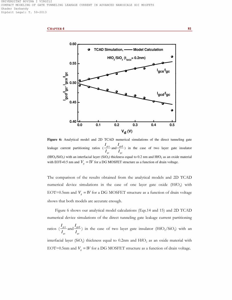
CHAPTER 4 81
0.0 0.1 0.2 0.3 0.4 0.50.40
0.45
0.50
0.55
0.60
HfO2/SiO
2 (t
SiO2= 0.2nm)
Igcd/Igc
I gc
d/Ig
c, I g
cs
/Ig
c
Vd (V)
TCAD Simulation, Model Calculation
Igcs/Igc
Figure 6: Analytical model and 2D TCAD numerical simulations of the direct tunneling gate
leakage current partitioning ratios (gcs
gc
I
Iand
gcd
gc
I
I) in the case of two layer gate insulator
(HfO2/SiO2) with an interfacial layer (SiO2) thickness equal to 0.2 nm and HfO2 as an oxide material
with EOT=0.5 nm and 1gV V= for a DG MOSFET structure as a function of drain voltage.
The comparison of the results obtained from the analytical models and 2D TCAD
numerical device simulations in the case of one layer gate oxide (HfO2) with
EOT=0.5nm and 1gV V= for a DG MOSFET structure as a function of drain voltage
shows that both models are accurate enough.
Figure 6 shows our analytical model calculations (Eqs.14 and 15) and 2D TCAD
numerical device simulations of the direct tunneling gate leakage current partitioning
ratios (gcs
gc
I
Iand
gcd
gc
I
I) in the case of two layer gate insulator (HfO2/SiO2) with an
interfacial layer (SiO2) thickness equal to 0.2nm and HfO2 as an oxide material with
EOT=0.5nm and 1gV V= for a DG MOSFET structure as a function of drain voltage.
UNIVERSITAT ROVIRA I VIRGILI COMPACT MODELING OF GATE TUNNELING LEAKAGE CURRENT IN ADVANCED NANOSCALE SOI MOSFETS Ghader Darbandy Dipòsit Legal: T. 59-2013
82 GHADER DARBANDY
There is a good agreement between the results from our analytical model and 2D
TCAD numerical device simulations. Figure 5 and Figure 6 show the gate leakage
current split equally between source and drain for drain voltage equal to 0 (Vd=0),
while the ratio of the leakage current that goes to the source increase by drain voltage,
and at the same time the ratio of the gate current goes to the drain decrease. In fact
increasing the ratio of the source component exactly is compensated by decreasing the
ratio of drain component in terms of drain voltage.
6) Conclusion
In this study we presented a model of the partitioning of the gate to channel
tunneling leakage current into the source and drain components based on a recently
developed, complete, surface potential-based compact MOSFET model and a compact
analytical gate leakage current model for a nanoscale DG MOSFETs structure. The
influence and impact of the thickness of the interfacial SiO2 layer on the gate-drain and
gate-source components has been shown. The model works well from the numerical
simulation point of view (Silvaco Atlas). The proposed model provides additional
insight into the gate leakage components and can be very useful to address the impact
of the gate leakage current on DG MOSFET device and circuit performance.
References
[1] P. J. Wright and K. C. Saraswat, “Thickness limitations of SiO2 gate dielectrics for
MOS ULSI,” IEEE Trans. Elec. Dev., vol.37 (8), pp. 1884, Aug. 1990.
[2] Juan C. Ranuarez, M. Jamal Deen and Chih-Hung Chen., A Review of Gate
Tunneling Current in MOS Devices, Microelectronics Reliability, Vol. 46(12), pp.
1939-1956 (2006).
[3] Y. Taur, D. A. Buchanan, W. Chen, D. J. Frank, K. E. Ismail, S. H. Lo, G. Sai-
Halasz, R. Viswanathan, and et al., “CMOS scaling into nanometer regime”, Proc. of
the IEEE, vol. 85, pp. 486–504, Apr. 1997.
UNIVERSITAT ROVIRA I VIRGILI COMPACT MODELING OF GATE TUNNELING LEAKAGE CURRENT IN ADVANCED NANOSCALE SOI MOSFETS Ghader Darbandy Dipòsit Legal: T. 59-2013
CHAPTER 4 83
[4] K. M. Cao, W. C. Lee, W. Liu, P. Su, S. K. H. Fung, J. X. An, B. Yu, and C. Hu,
“BSIM4 gate leakage model including source–drain partition,” in IEDM Tech. Dig., San
Francisco, CA, Dec, 2000, p. 815–818.
[5] R. van Langevelde, A. J. Scholten, R. Duffy, F. N. Cubaynes, M. J. Knitel, and D. B.
M. Klaassen, “Gate current: modeling, ∆L extraction and impact on RF
performance,” in IEDM Tech. Dig., 2001, pp.289–292.
[6] W-K. Shih, R. Rios, P. Packan, K. Mistry, T. Abbott, “A general partition scheme
for gate leakage current suitable for MOSFET compact models,” in IEDM Tech. Dig.,
2001, pp. 293–296
[7] A. Cerdeira, O. Moldovan, B. Iñiguez and M. Estrada, “Modeling of potentials and
threshold voltage for symmetric doped double-gate MOSFETs”, Solid-State
Electronics, vol. 52, no. 5, pp. 830-837, May 2008.
[8] A. Cerdeira, B. Iñiguez and M. Estrada, “Compact model for short channel
symmetric doped double-gate MOSFET,”, Solid-State Electronics, vol. 52, no. 7, pp.
1064-1070, July 2008.
[9] G. Darbandy, R. Ritzenthaler, F. Lime, I. Garduño, M. Estrada, A. Cerdeira and B.
Iñiguez, “Analytical Modeling of the Gate Tunneling Leakage for the Determination of
Adequate High-k Dielectrics in Double-Gate SOI MOSFETs at the 22 nm node”,
Solid-State Electronics, 54 (2010), pp. 1083-1087.
[10] G. Darbandy, R. Ritzenthaler, F. Lime, I. Garduño, M. Estrada, A. Cerdeira and B.
Iñiguez, “Analytical Modeling of Direct Tunneling Current through SiO2/high-k Gate
Stacks for the Determination of Suitable High-k Dielectrics for Nanoscale Double-
Gate MOSFETs”, Semicond. Sci. Technol. 26 (2011) 045002
[11] Merzbacher E 1961, 1970 Quantum Mechanics (New York: Wiley)
[12] Fromhold A T 1981 Quantum Mechanics for Applied Physics and Engineering
(New York: Dover).
[13] J. Robertson, “High dielectric constant oxides”, Eur Phys J Appl Phys, 2004; 28(3):
265–91.
UNIVERSITAT ROVIRA I VIRGILI COMPACT MODELING OF GATE TUNNELING LEAKAGE CURRENT IN ADVANCED NANOSCALE SOI MOSFETS Ghader Darbandy Dipòsit Legal: T. 59-2013
84 GHADER DARBANDY
[14] M. V. Dunga, X. Xi, J. He, I. Polishchuk, Q. Lu, M. Chan, A. M. Niknejad, and C.
Hu “Modeling of Direct Tunneling Current in Multi-Layer Gate Stacks”, in Proc of the
Workshop on Compact Modeling (WCM), Nanotech Conference, 2003, p. 306-309.
[15] K. F. Schuegraf and C. Hu, “Hole Injection SiO Breakdown model for very low
voltage lifetime extrapolation,” IEEE Trans. Electron Devices, vol. 41, no. 5, pp. 761–
767, 1994
[16] K. F. Schuegraf, C. C. King, and C. Hu, “Ultra-thin silicon dioxide leakage current
and scaling limit,” in: Symposium on VLSI Technology, Digest of Technical Papers,
1992, p. 18
[17] W-C. Lee, C. Hu. “Modeling CMOS tunneling currents through ultrathin gate
oxide due to conduction and valence-band electron and hole tunneling”. IEEE Trans
Electron Dev 2001; 48(7):1366-73.
[18] T. Kauerauf, B. Govoreanu, R. Degraeve, G. Groeseneken, H. Maes. “Finding the
gate stack with the lowest leakage current”, Solid State Electron 2005; 49(5):695–701.
[19] M. Houssa, M. Tuominen, M. Naili, V. Afanas’ev, A. Stesmans, S. Haukka, M. M.
Heyns. “Trap-assisted tunneling in high permittivity gate dielectric stacks”. J Appl Phys
2000; 87(12): 8615.
[20] GD. Wilk, RM. Wallace, JM. Anthony. “High-k gate dielectrics: current status and
materials properties”. J. Appl. Phys., vol. 89, pp. 5243–5275, 2001
[21] S. I. Garduño, A. Cerdeira M. Estrada, “Inclusion of Direct Tunneling Gate
Current in the Symmetric Doped Double Gate MOSFETs Model”, 2009 6th
International Conference on Electrical Engineering, Computing Science and Automatic Control
(CCE 2009).
[22] Hitender Kumar Tyagi, P. J. George “Tunneling currents through ultra thin
HfO2/Al2O3/HfO2 triple layer gate dielectrics for advanced MIS devices” J mater Sci:
Mater Electron (2008) 19:902-907.
UNIVERSITAT ROVIRA I VIRGILI COMPACT MODELING OF GATE TUNNELING LEAKAGE CURRENT IN ADVANCED NANOSCALE SOI MOSFETS Ghader Darbandy Dipòsit Legal: T. 59-2013
85
Chapter 5
Temperature Dependent Compact Modeling of Gate
Tunneling Leakage Current in Double Gate MOSFETs
The temperature dependence of the gate leakage current has been developed for
Double Gate (DG) MOSFETs. This model is compared with experimental data
measured in Trigate MOSFETs at various temperatures with SiON as a dielectric
material and SiO2 as an interfacial layer. The gate leakage current measurements at
different temperatures show two different transport mechanisms, direct tunneling
(DT) gate leakage and Trap-Assisted-Tunneling (TAT) current. Our analysis based on
leakage current measurements in the above threshold regime for different temperatures
shows that the DT current is clearly dominant over the TAT, while the opposite
happens below threshold. Our model is able to explain the gate tunneling current in
terms of gate voltage for different temperatures. The results of the DT current in the
strong inversion regime and TAT in the subthreshold regime show good agreement
with temperature dependent measurements.
UNIVERSITAT ROVIRA I VIRGILI COMPACT MODELING OF GATE TUNNELING LEAKAGE CURRENT IN ADVANCED NANOSCALE SOI MOSFETS Ghader Darbandy Dipòsit Legal: T. 59-2013
86 GHADER DARBANDY
1) Introduction
The scaling down of gate oxide thickness in advanced CMOS technology causes an
increase of gate leakage current due to the increasing carrier tunneling between gate
and channel [1, 2]. Understanding the gate current transport mechanisms is important
in order to develop accurate design-oriented models.
The temperature dependence of the surface potential induces a decrease of the
threshold voltage with increasing temperature. As a result, an increase of the carriers in
the channel takes place with temperature. Besides, the barrier height between gate and
channel decreases with temperature. Therefore, the gate leakage current increases at
higher temperatures [3, 4]. It causes undesirable effects on the device performance [5,
6]; it increases power dissipation and deteriorates the circuit stability [7]. Temperature
dependent measurements of the gate leakage current have been used to study and
understanding carrier transport through different gate dielectric materials [8, 9].
The high-k dielectric materials are alternative gate oxide materials [10, 11] for the
coming nanoscale CMOS generations in order to suppress the gate leakage current.
Analytical expressions are presented to model the gate leakage current as a function of
applied gate and drain voltages for DG MOSFETs [12]. The presence of electron trap
levels in SiON can result in a significant leakage current at low electric field
(subthreshold regime) in which electrons gain sufficient energy to tunnel through the
oxide material [13]. In this chapter we present the incorporation of the temperature
dependence for the DT and TAT in FinFETs (modeled as DG MOSFETs) assuming a
two dielectric layer gate stack (being SiO2 as an interfacial layer). Furthermore, for that
purpose, we have extended the gate current models to the case of a two dielectric layer
gate stack. The comparison between our model calculations demonstrates that the
model can accurately reproduce the gate leakage current behavior through SiON/SiO2
gate oxide for different temperatures.
UNIVERSITAT ROVIRA I VIRGILI COMPACT MODELING OF GATE TUNNELING LEAKAGE CURRENT IN ADVANCED NANOSCALE SOI MOSFETS Ghader Darbandy Dipòsit Legal: T. 59-2013
CHAPTER 5 87
2) DG FinFET Structure and Temperature Effects
The DG FinFET structure under analysis and related potential profile showing DT
and TAT mechanisms through SiON/SiO2 as gate oxide materials are shown in Figure
1. The effect of temperature has been taken into account by considering its
dependence on the thermal voltage, flat band voltage, carrier concentration, Fermi
level and the Si-SiO2 barrier height of the carriers [14, 15].
A) Thermal Voltage
The thermal voltage (t
KT
qφ = ) at room temperature is equal to 0.026 (V) where q is
the electronic charge, T is temperature in Kelvin and K is Boltzmann constant. Higher
thermal energy gives electrons more energy for jumping from the valence into the
conduction band. Thus, the number of carriers of an intrinsic semiconductor increases
with temperature which is taken into account by thermal voltage.
B) Carrier Concentration and Fermi Level
The electron concentration and the Fermi potential in the case of an n-type
semiconductor are calculated:
eFq
KTi
n n
φ− ×
= × (1)
The Fermi potential becomes:
a
F
i i
NK T n K TL n L n
q n q nφ
− −= × = ×
(2)
where ni is the intrinsic carriers (electrons) concentration at T and is a function of
temperature and Na is the acceptor atoms concentration. Hence the Fermi potential is
calculated using (2) and will be shifted with the temperature.
UNIVERSITAT ROVIRA I VIRGILI COMPACT MODELING OF GATE TUNNELING LEAKAGE CURRENT IN ADVANCED NANOSCALE SOI MOSFETS Ghader Darbandy Dipòsit Legal: T. 59-2013
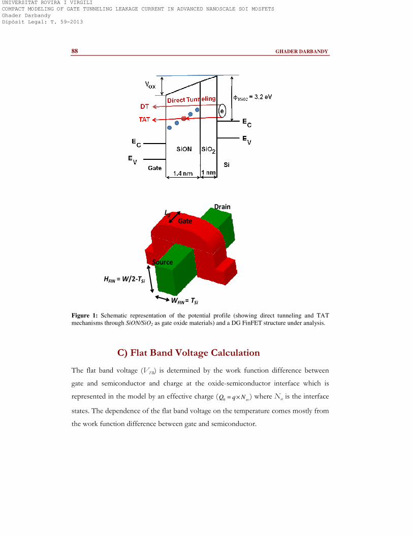
88 GHADER DARBANDY
WFIN = TSi
HFIN = W/2-TSi
Source
Drain
GateLg
Figure 1: Schematic representation of the potential profile (showing direct tunneling and TAT
mechanisms through SiON/SiO2 as gate oxide materials) and a DG FinFET structure under analysis.
C) Flat Band Voltage Calculation
The flat band voltage (VFB) is determined by the work function difference between
gate and semiconductor and charge at the oxide-semiconductor interface which is
represented in the model by an effective charge (0 ss
Q q N= × ) where Nss is the interface
states. The dependence of the flat band voltage on the temperature comes mostly from
the work function difference between gate and semiconductor.
UNIVERSITAT ROVIRA I VIRGILI COMPACT MODELING OF GATE TUNNELING LEAKAGE CURRENT IN ADVANCED NANOSCALE SOI MOSFETS Ghader Darbandy Dipòsit Legal: T. 59-2013
CHAPTER 5 89
The flat band voltage considering the effects of the effective charge and work function
difference between gate and semiconductor as a function of temperature becomes:
0( , , ) ( , )( )
FB a MS a
OX
QV N T EOT N T
C EOTφ= − (3)
where ( , )MS a
N Tφ is the work function difference between gate and Si, Equivalent
Oxide Thickness is EOT and COX is the oxide capacitance.
D) Dielectric-Semiconductor Barrier Height
We extracted the Si-SiO2 barrier height to the carrier ( 2BSiOφ ) at different temperatures.
We observed that it shows a linear decrease of 2BSiO
φ with temperature. As a result, an
expression of the 2BSiOφ accounting for the observed linear dependence with
temperature can be incorporated into our temperature dependent model.
3) Direct Tunneling Gate Leakage Current
We developed a temperature dependent analytical model of the direct tunneling gate
leakage current based on a proper WKB approximation for DG MOSFETs, using our
previous compact model for the potential and drain current [16, 17]. It was
demonstrated that this model can also be applied to sufficiently narrow FinFETs. We
derived the following gate tunneling leakage current expression [11, 12] for two
dielectric layer gate stacks (in our case, SiON/SiO2):
( )
2 0 2
3 3
2 22 2 2 2 2
2
1, ,
2
8exp 10 2
3
8exp 10
3
g fbp a defA
GDT gm
SiO SiO
SiO SiON SiON SiO BSiO BSiO im
SiO
SiON im
V V N T EOT VF
J Qk T
k T k T Fraction q Vm q
h k V q q
h
ε
φ φπ
π
−
− − ×
= × × × ×
× + × − × × − × × × × × × − × ×
− ×
3 3
2 22 2 2
2
2SiO SiON SiON SiO BSiON im BSiON im
SiON
SiO im
k T k T Fraction q V q Vm q
k V q q
φ φ−
× + × − × × − × × × × × × − ×
(4)
where kSiO2 is SiO2 dielectric constant, the permittivity of vacuum is 0ε , Vg is the
applied gate voltage, Vfbp is the flat band voltage corresponding to the channel region,
Vdef is effective drain voltage [16, 17], TSiO2 is the SiO2 thickness, h is the Plank`s
UNIVERSITAT ROVIRA I VIRGILI COMPACT MODELING OF GATE TUNNELING LEAKAGE CURRENT IN ADVANCED NANOSCALE SOI MOSFETS Ghader Darbandy Dipòsit Legal: T. 59-2013
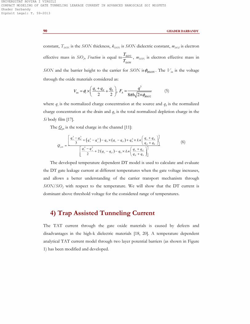
90 GHADER DARBANDY
constant, TSiON is the SiON thickness, kSiON is SiON dielectric constant, mSiO2 is electron
effective mass in SiO2, Fraction is equal to 2SiO
SiON
T
T, mSiON is electron effective mass in
SiON and the barrier height to the carrier for SiON is BSiONφ . The Vim is the voltage
through the oxide materials considered as:
2 2
s d bim t
q q qV φ
+ = × +
,
3
28 2
A
BSiO
qF
hπ φ=
× (5)
where qs is the normalized charge concentration at the source and qd is the normalized
charge concentration at the drain and qb is the total normalized depletion charge in the
Si body film [17].
The Qgm is the total charge in the channel [11]:
( ) ( )
( )
3 32 2 2
2 2
3
22
d
d
s d s ds b s d b
d b
gm
s s ds d b
d b
q q q qq q q q q q Ln
q qQ
q q q qq q q Ln
q q
− ++ − − × − + ×
+ = − +
+ − − × +
(6)
The developed temperature dependent DT model is used to calculate and evaluate
the DT gate leakage current at different temperatures when the gate voltage increases,
and allows a better understanding of the carrier transport mechanism through
SiON/SiO2 with respect to the temperature. We will show that the DT current is
dominant above threshold voltage for the considered range of temperatures.
4) Trap Assisted Tunneling Current
The TAT current through the gate oxide materials is caused by defects and
disadvantages in the high-k dielectric materials [18, 20]. A temperature dependent
analytical TAT current model through two layer potential barriers (as shown in Figure
1) has been modified and developed.
UNIVERSITAT ROVIRA I VIRGILI COMPACT MODELING OF GATE TUNNELING LEAKAGE CURRENT IN ADVANCED NANOSCALE SOI MOSFETS Ghader Darbandy Dipòsit Legal: T. 59-2013
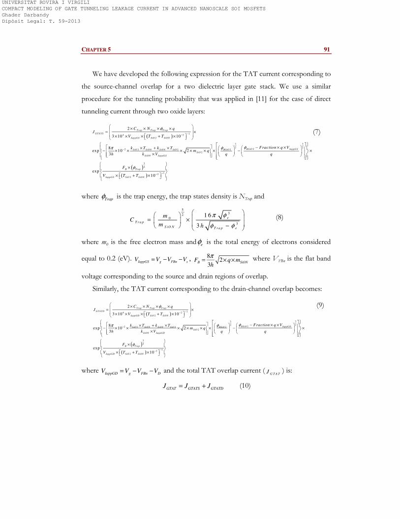
CHAPTER 5 91
We have developed the following expression for the TAT current corresponding to
the source-channel overlap for a two dielectric layer gate stack. We use a similar
procedure for the tunneling probability that was applied in [11] for the case of direct
tunneling current through two oxide layers:
( )1
4 2
2
33
2222 2 2 2
2
2
3 10 10
8exp 10 2
3
Trap Trap Trap
GTATS
IappGS SiO SiON
BSiO IappGSSiO SiON SiON SiO BSiOSiO
SiON IappG S
C N qJ
V T T
Fraction q Vk T k Tm q
h k V q q
φ
φφπ
−−
−
× × × × = × × × × + ×
− × × × + × − × × × × × × − ×
( )( )
3
2
12
2
exp10
B Trap
IappGS SiO SiON
F
V T T
φ−−
×
×
× + ×
(7)
where Trapφ is the trap energy, the trap states density is NTrap and
532
0
3
1 6
3
e
T r a p
S iO N T r a p e
mC
m h
π φ
φ φ
= × −
(8)
where m0 is the free electron mass and eφ is the total energy of electrons considered
equal to 0.2 (eV). IappGS g FBn sV V V V= − − , 8
23
B SiONF q mh
π= × × where VFBn is the flat band
voltage corresponding to the source and drain regions of overlap.
Similarly, the TAT current corresponding to the drain-channel overlap becomes:
( )1
4 2
2
33
2222 2 2 2
2
2
3 10 10
8exp 10 2
3
Trap Trap Trap
GTATD
IappGD SiO SiON
BSiO IappGDSiO SiON SiON SiO BSiOSiO
SiON IappGD
C N qJ
V T T
Fraction q Vk T k Tm q
h k V q q
φ
φφπ
−−
−
× × × × = × × × × + ×
− × × × + × − × × × × × × − ×
( )( )
3
2
12
2
exp10
B Trap
IappGD SiO SiON
F
V T T
φ−
−
×
×
× + ×
(9)
where IappGD g FBn D
V V V V= − − and the total TAT overlap current (G T A TJ ) is:
GTAT GTATS GTATDJ J J= + (10)
UNIVERSITAT ROVIRA I VIRGILI COMPACT MODELING OF GATE TUNNELING LEAKAGE CURRENT IN ADVANCED NANOSCALE SOI MOSFETS Ghader Darbandy Dipòsit Legal: T. 59-2013
92 GHADER DARBANDY
The tunneling probability of carriers is exponentially dependent on the barrier
height that they have to cross through the dielectric layers. The presence of the trap
inside the dielectric materials splits the energy barrier in two parts. An increasing
temperature will also decrease the barrier height, whereas increasing exponentially the
probability of the total tunneling current. Once the transition probabilities of the
carriers are known, the trap-assisted tunneling current can be obtained. The model
calculations at different temperatures give the precise gate leakage at low electric field.
5) Results and Discussion
The device structure under analysis and potential profile showing the DT and TAT
mechanisms through two layer oxide materials (SiON/SiO2) is shown in Figure 1. The
DT gate leakage current calculations for different temperatures (using our model) in
strong inversion as well as TAT in the subthreshold regime has been compared with
experimental measurements. The temperature dependent Si-SiO2 barrier height to the
carrier (2BSiO
φ ) was extracted and it resulted a linear decrease of 2BSiO
φ with
temperature. Therefore, an expression of the 2BSiOφ giving the observed linear
dependence with temperature is incorporated into our model. The measurements have
been performed on FinFET devices with an EOT equal to 1.9nm through SiON/SiO2
as a gate oxide material for different bias and temperatures.
A) Direct Tunneling Gate Leakage Current
The model calculations (4) and experimental measurements of the DT current as a
function of applied gate voltage for different temperatures are shown in Figure 2 with
channel length (LG) equal to 10 micrometer (u) at VD=0.05(V) and VD=1(V). As can
be seen in Figure 2, the gate leakage current will increase with increasing temperature,
which is attributed to the increase of carriers in the channel and the decrease of the
barrier height. We have considered a linear decrease of the barrier height for the
carriers through the gate oxide materials with temperature.
UNIVERSITAT ROVIRA I VIRGILI COMPACT MODELING OF GATE TUNNELING LEAKAGE CURRENT IN ADVANCED NANOSCALE SOI MOSFETS Ghader Darbandy Dipòsit Legal: T. 59-2013
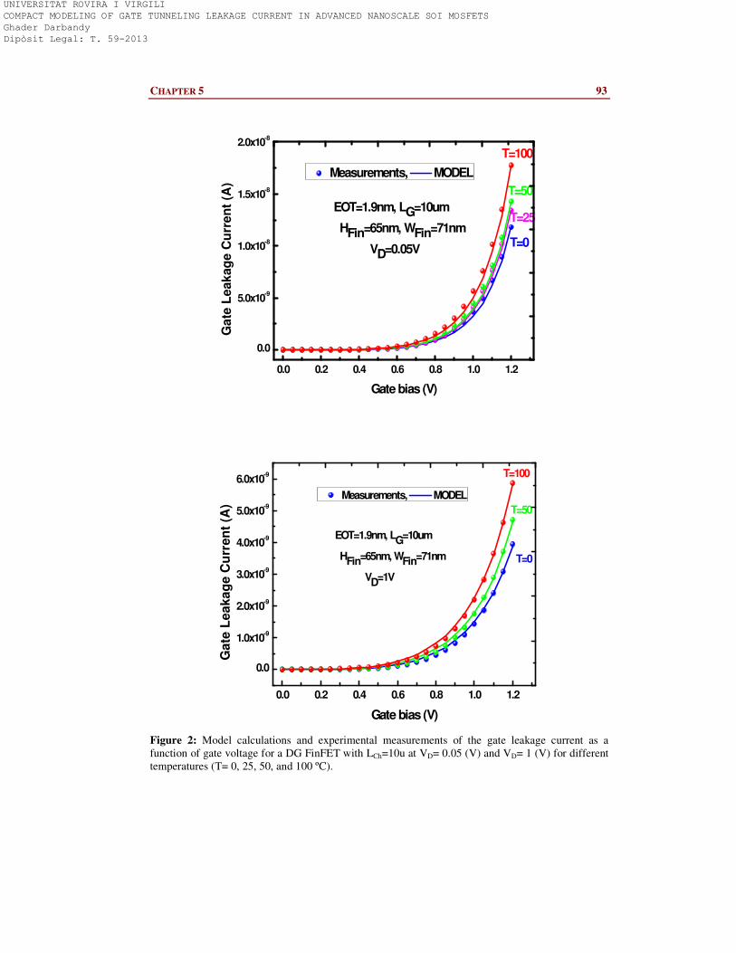
CHAPTER 5 93
0.0 0.2 0.4 0.6 0.8 1.0 1.2
0.0
5.0x10⁻⁹
1.0x10⁻⁸
1.5x10⁻⁸
2.0x10⁻⁸
T=50
EOT=1.9nm, LG=10um
HFin=65nm, WFin=71nm
VD=0.05V
T=100
T=0
T=25G
ate
Le
ak
ag
e C
urr
en
t (A
)
Gate bias (V)
Measurements, MODEL
0.0 0.2 0.4 0.6 0.8 1.0 1.2
0.0
1.0x10⁻⁹
2.0x10⁻⁹
3.0x10⁻⁹
4.0x10⁻⁹
5.0x10⁻⁹
6.0x10⁻⁹
T=50
EOT=1.9nm, LG=10um
HFin=65nm, WFin=71nm
VD=1V
T=100
T=0
Ga
te L
ea
ka
ge C
urr
en
t (A
)
Gate bias (V)
Measurements, MODEL
Figure 2: Model calculations and experimental measurements of the gate leakage current as a
function of gate voltage for a DG FinFET with LCh=10u at VD= 0.05 (V) and VD= 1 (V) for different
temperatures (T= 0, 25, 50, and 100 ºC).
UNIVERSITAT ROVIRA I VIRGILI COMPACT MODELING OF GATE TUNNELING LEAKAGE CURRENT IN ADVANCED NANOSCALE SOI MOSFETS Ghader Darbandy Dipòsit Legal: T. 59-2013
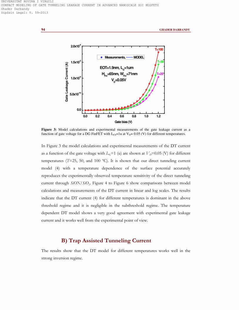
94 GHADER DARBANDY
0.0 0.2 0.4 0.6 0.8 1.0 1.2
0.0
5.0x10⁻¹⁰
1.0x10⁻⁹
1.5x10⁻⁹
2.0x10⁻⁹
T=50
EOT=1.9nm, LG=1um
HFin
=65nm, WFin
=71nm
VD=0.05V
T=100
T=25
Gate
Lea
kag
e C
urr
en
t (A
)
Gate bias (V)
Measurements, MODEL
Figure 3: Model calculations and experimental measurements of the gate leakage current as a
function of gate voltage for a DG FinFET with LCh=1u at VD= 0.05 (V) for different temperatures.
In Figure 3 the model calculations and experimental measurements of the DT current
as a function of the gate voltage with LG=1 (u) are shown at VD=0.05 (V) for different
temperatures (T=25, 50, and 100 ºC). It is shown that our direct tunneling current
model (4) with a temperature dependence of the surface potential accurately
reproduces the experimentally observed temperature sensitivity of the direct tunneling
current through SiON/SiO2. Figure 4 to Figure 6 show comparisons between model
calculations and measurements of the DT current in linear and log scales. The results
indicate that the DT current (4) for different temperatures is dominant in the above
threshold regime and it is negligible in the subthreshold regime. The temperature
dependent DT model shows a very good agreement with experimental gate leakage
current and it works well from the experimental point of view.
B) Trap Assisted Tunneling Current
The results show that the DT model for different temperatures works well in the
strong inversion regime.
UNIVERSITAT ROVIRA I VIRGILI COMPACT MODELING OF GATE TUNNELING LEAKAGE CURRENT IN ADVANCED NANOSCALE SOI MOSFETS Ghader Darbandy Dipòsit Legal: T. 59-2013
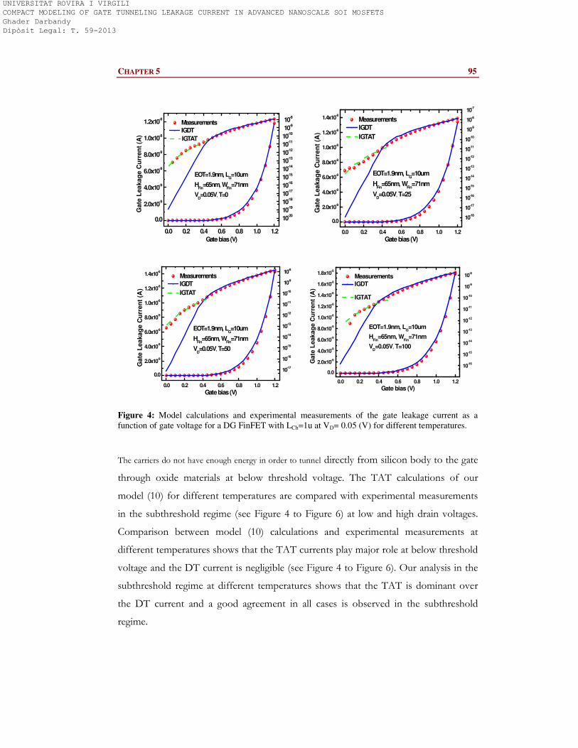
CHAPTER 5 95
0.0 0.2 0.4 0.6 0.8 1.0 1.2
0.0
2.0x10⁻⁹
4.0x10⁻⁹
6.0x10⁻⁹
8.0x10⁻⁹
1.0x10⁻⁸
1.2x10⁻⁸
10-20
10-19
10-18
10-17
10-16
10-15
10-14
10-13
10-12
10-11
10-10
10-9
10-8
EOT=1.9nm, LG=10um
HFin
=65nm, WFin
=71nm
VD=0.05V, T=0
Gate
Lea
kag
e C
urr
en
t (A
)
Gate bias (V)
Measurements
IGDT
IGTAT
0.0 0.2 0.4 0.6 0.8 1.0 1.2
0.0
2.0x10⁻⁹
4.0x10⁻⁹
6.0x10⁻⁹
8.0x10⁻⁹
1.0x10⁻⁸
1.2x10⁻⁸
1.4x10⁻⁸
10-18
10-17
10-16
10-15
10-14
10-13
10-12
10-11
10-10
10-9
10-8
10-7
EOT=1.9nm, LG=10um
HFin
=65nm, WFin
=71nm
VD=0.05V, T=25
Gate
Lea
ka
ge C
urr
en
t (A
)
Gate bias (V)
Measurements
IGDT
IGTAT
0.0 0.2 0.4 0.6 0.8 1.0 1.2
0.0
2.0x10⁻⁹
4.0x10⁻⁹
6.0x10⁻⁹
8.0x10⁻⁹
1.0x10⁻⁸
1.2x10⁻⁸
1.4x10⁻⁸
10-17
10-16
10-15
10-14
10-13
10-12
10-11
10-10
10-9
10-8
EOT=1.9nm, LG=10um
HFin
=65nm, WFin
=71nm
VD=0.05V, T=50
Ga
te L
ea
ka
ge C
urr
en
t (A
)
Gate bias (V)
Measurements
IGDT
IGTAT
0.0 0.2 0.4 0.6 0.8 1.0 1.2
0.0
2.0x10⁻⁹
4.0x10⁻⁹
6.0x10⁻⁹
8.0x10⁻⁹
1.0x10⁻⁸
1.2x10⁻⁸
1.4x10⁻⁸
1.6x10⁻⁸
1.8x10⁻⁸
10-16
10-15
10-14
10-13
10-12
10-11
10-10
10-9
10-8
EOT=1.9nm, LG=10um
HFin
=65nm, WFin
=71nm
VD=0.05V, T=100
Gate
Le
ak
ag
e C
urr
en
t (A
)
Gate bias (V)
Measurements
IGDT
IGTAT
Figure 4: Model calculations and experimental measurements of the gate leakage current as a
function of gate voltage for a DG FinFET with LCh=1u at VD= 0.05 (V) for different temperatures.
The carriers do not have enough energy in order to tunnel directly from silicon body to the gate
through oxide materials at below threshold voltage. The TAT calculations of our
model (10) for different temperatures are compared with experimental measurements
in the subthreshold regime (see Figure 4 to Figure 6) at low and high drain voltages.
Comparison between model (10) calculations and experimental measurements at
different temperatures shows that the TAT currents play major role at below threshold
voltage and the DT current is negligible (see Figure 4 to Figure 6). Our analysis in the
subthreshold regime at different temperatures shows that the TAT is dominant over
the DT current and a good agreement in all cases is observed in the subthreshold
regime.
UNIVERSITAT ROVIRA I VIRGILI COMPACT MODELING OF GATE TUNNELING LEAKAGE CURRENT IN ADVANCED NANOSCALE SOI MOSFETS Ghader Darbandy Dipòsit Legal: T. 59-2013
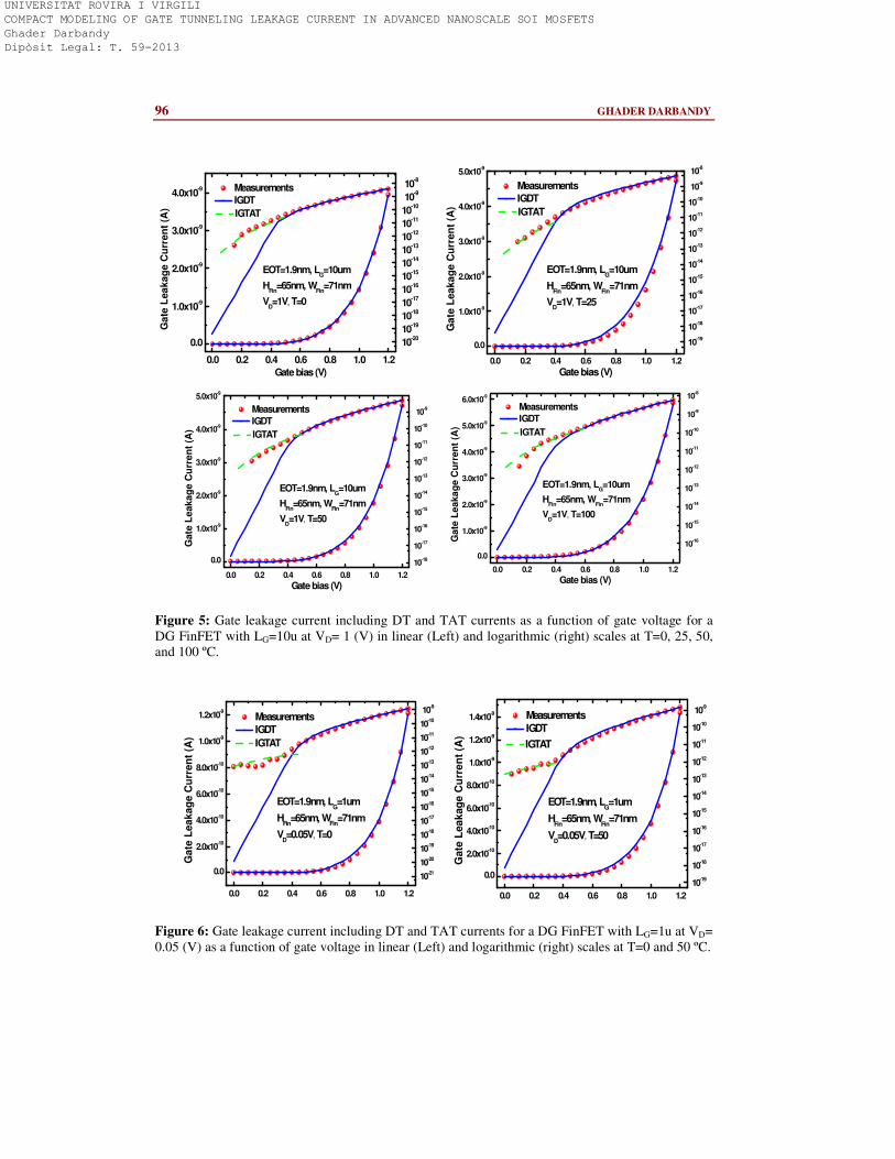
96 GHADER DARBANDY
0.0 0.2 0.4 0.6 0.8 1.0 1.2
0.0
1.0x10⁻⁹
2.0x10⁻⁹
3.0x10⁻⁹
4.0x10⁻⁹
10-20
10-19
10-18
10-17
10-16
10-15
10-14
10-13
10-12
10-11
10-10
10-9
10-8
EOT=1.9nm, LG=10um
HFin
=65nm, WFin
=71nm
VD=1V, T=0
Ga
te L
ea
ka
ge
Cu
rre
nt
(A)
Gate bias (V)
Measurements
IGDT
IGTAT
0.0 0.2 0.4 0.6 0.8 1.0 1.2
0.0
1.0x10⁻⁹
2.0x10⁻⁹
3.0x10⁻⁹
4.0x10⁻⁹
5.0x10⁻⁹
10-19
10-18
10-17
10-16
10-15
10-14
10-13
10-12
10-11
10-10
10-9
10-8
EOT=1.9nm, LG=10um
HFin
=65nm, WFin
=71nm
VD=1V, T=25
Ga
te L
ea
ka
ge C
urr
en
t (A
)
Gate bias (V)
Measurements
IGDT
IGTAT
0.0 0.2 0.4 0.6 0.8 1.0 1.2
0.0
1.0x10⁻⁹
2.0x10⁻⁹
3.0x10⁻⁹
4.0x10⁻⁹
5.0x10⁻⁹
10-18
10-17
10-16
10-15
10-14
10-13
10-12
10-11
10-10
10-9
EOT=1.9nm, LG=10um
HFin
=65nm, WFin
=71nm
VD=1V, T=50
Gate
Le
ak
ag
e C
urr
en
t (A
)
Gate bias (V)
Measurements
IGDT
IGTAT
0.0 0.2 0.4 0.6 0.8 1.0 1.2
0.0
1.0x10⁻⁹
2.0x10⁻⁹
3.0x10⁻⁹
4.0x10⁻⁹
5.0x10⁻⁹
6.0x10⁻⁹
10-16
10-15
10-14
10-13
10-12
10-11
10-10
10-9
10-8
EOT=1.9nm, LG=10um
HFin
=65nm, WFin
=71nm
VD=1V, T=100
Gate
Leaka
ge C
urr
en
t (A
)
Gate bias (V)
Measurements
IGDT
IGTAT
Figure 5: Gate leakage current including DT and TAT currents as a function of gate voltage for a
DG FinFET with LG=10u at VD= 1 (V) in linear (Left) and logarithmic (right) scales at T=0, 25, 50,
and 100 ºC.
0.0 0.2 0.4 0.6 0.8 1.0 1.2
0.0
2.0x10⁻¹⁰
4.0x10⁻¹⁰
6.0x10⁻¹⁰
8.0x10⁻¹⁰
1.0x10⁻⁹
1.2x10⁻⁹
10-21
10-20
10-19
10-18
10-17
10-16
10-15
10-14
10-13
10-12
10-11
10-10
10-9
EOT=1.9nm, LG=1um
HFin
=65nm, WFin
=71nm
VD=0.05V, T=0
Ga
te L
ea
ka
ge
Cu
rre
nt
(A)
Measurements
IGDT
IGTAT
0.0 0.2 0.4 0.6 0.8 1.0 1.2
0.0
2.0x10⁻¹⁰
4.0x10⁻¹⁰
6.0x10⁻¹⁰
8.0x10⁻¹⁰
1.0x10⁻⁹
1.2x10⁻⁹
1.4x10⁻⁹
10-19
10-18
10-17
10-16
10-15
10-14
10-13
10-12
10-11
10-10
10-9
EOT=1.9nm, LG=1um
HFin
=65nm, WFin
=71nm
VD=0.05V, T=50
Gate
Lea
kag
e C
urr
en
t (A
)
Measurements
IGDT
IGTAT
Figure 6: Gate leakage current including DT and TAT currents for a DG FinFET with LG=1u at VD=
0.05 (V) as a function of gate voltage in linear (Left) and logarithmic (right) scales at T=0 and 50 ºC.
UNIVERSITAT ROVIRA I VIRGILI COMPACT MODELING OF GATE TUNNELING LEAKAGE CURRENT IN ADVANCED NANOSCALE SOI MOSFETS Ghader Darbandy Dipòsit Legal: T. 59-2013
CHAPTER 5 97
The results show that the temperature dependent of DT and TAT currents (4 and 10)
have to be taken into account for a precise modeling of the total gate leakage current
through the gate dielectric materials in both the strong inversion and the subthreshold
regimes at different temperatures.
6) Conclusion
Temperature dependent analytical models of the DT current in inversion region
and the TAT current in subthreshold regime have been developed for DG FinFET
with a two dielectric layers gate stack such as SiON/SiO2. The comparison between the
model calculations and experimental measurements for different temperatures shows
that the DT current is clearly dominant over TAT above threshold voltage, whereas it
is negligible below threshold voltage and TAT becomes dominant. The temperature
dependence of the gate current has been accurately modeled in both the strong
inversion and the subthreshold regimes and shows good agreement with the
experimental measurements.
References
[1] K.Roy, Fellow, IEEE, S. Mukopadhyay, Student Member, IEEE, and H.
Mahmoodi-Meimand, Student Member, IEEE, “Leakage Current Mechanisms and
Leakage Reduction Techniques in Deep Submicrometer CMOS Circuits”, Proceedings of
the IEEE, VOL. 91, NO. 2, February 2003.
[2] Jonathan P. Halter and Farid N. Najm, “A Gate-Level Leakage Power Reduction
Method for Ultra-Low-Power CMOS Circuits” IEEE 1997 Custom Integrated Circuits
Conference.
[3] Zhen Xu, Michel Houssa, Stefan De Gendt, and Marc Heyns, “Polarity effect on
the temperature dependence of leakage current through HfO2/SiO2 gate dielectric
stacks”, Appl. Phys. Lett. 80, 1975 (2002).
UNIVERSITAT ROVIRA I VIRGILI COMPACT MODELING OF GATE TUNNELING LEAKAGE CURRENT IN ADVANCED NANOSCALE SOI MOSFETS Ghader Darbandy Dipòsit Legal: T. 59-2013
98 GHADER DARBANDY
[4] Jau-Yi WU, Po-Wen Sze, Yeong-Her Wang, Mau-Phon Houng, “Temperature
effect on gate leakage currents in gate dielectric films of GaAs MOSFET”, Solid State
Electronics 45 (2001) 1999-2003.
[5] P. J. Wright and K. C. Saraswat, “Thickness limitations of SiO2 gate dielectrics for
MOS ULSI,” IEEE Trans. Elec. Dev., vol.37 (8), pp. 1884, Aug. 1990.
[6] Juan C. Ranuarez, M. Jamal Deen and Chih-Hung Chen., A Review of Gate
Tunneling Current in MOS Devices, Microelectronics Reliability, Vol. 46(12), pp.
1939-1956 (2006)
[7] Y. Taur, D. A. Buchanan, W. Chen, D. J. Frank, K. E. Ismail, S. H. Lo, G. Sai-
Halasz, R. Viswanathan, and et al., “CMOS scaling into nanometer regime”, Proc. of
the IEEE, vol. 85, pp. 486–504, Apr. 1997
[8] A J. C. Tinoco, M. Estrada, B. Iñiguez, and A. Cerdeira, "Conduction mechanisms
of silicon oxide/titanium oxide MOS stack structures," Microelectronics Reliability,
vol. 48, pp. 370-381, 2008.
[9] J. Kolodzey, E. A. Chowdhury, T. N. Adam, Q. Guohua, I. Rau, J. 0. Olowolafe, J.
S. Suehle, and C. Yuan, "Electrical conduction and dielectric breakdown in aluminum
oxide insulators on silicon," Electron Devices, IEEE Transactions on, vol. 47, pp. 121-
128, 2000.
[10] G. Darbandy, R. Ritzenthaler, F. Lime, I. Garduño, M. Estrada, A. Cerdeira and B.
Iñiguez, “Analytical Modeling of the Gate Tunneling Leakage for the Determination of
Adequate High-k Dielectrics in Double-Gate SOI MOSFETs at the 22 nm node”,
Solid-State Electronics, 54 (2010), pp. 1083-1087.
[11] G. Darbandy, R. Ritzenthaler, F. Lime, I. Garduño, M. Estrada, A. Cerdeira and B.
Iñiguez, “Analytical Modeling of Direct Tunneling Current through SiO2/high-k Gate
Stacks for the Determination of Suitable High-k Dielectrics for Nanoscale Double-
Gate MOSFETs”, Semicond. Sci. Technol. 26 (2011) 045002.
[12] S. I. Garduño, A. Cerdeira, M. Estrada, J. Alvarado, V. Kilchytska and D. Flandre,
“Contribution of carrier tunneling and gate induced drain leakage effects to the gate
and drain currents of fin–shaped field–effect transistors”, Journal of Applied Physics,
109, 084524 (2011).
UNIVERSITAT ROVIRA I VIRGILI COMPACT MODELING OF GATE TUNNELING LEAKAGE CURRENT IN ADVANCED NANOSCALE SOI MOSFETS Ghader Darbandy Dipòsit Legal: T. 59-2013
CHAPTER 5 99
[13] Isodiana Crupi, Robin Degraeve, Bogdan Govoreanu, David P. Brunco, Philippe
J. Roussel, and Jan Van Houdt, “Energy and Spatial Distribution of Traps in
SiO2/Al2O3 nMOSFETs”, IEEE Transactions on Device and Materials Reliability,
Vol. 6, No. 4, (2006).
[14] Jean-Pierre Colinge, Cynthia A. Colinge, Physics of Semiconductor Devices, Kluwer
Academic Publishers.
[15] C. Galup-Montoro, Marcio Cherem Schneide, MOSFET Modeling for Circuit
Analysis and Design, World Scientific Publishing Co. Pte. Ltd.
[16] A. Cerdeira, O. Moldovan, B. Iñiguez and M. Estrada, “Modeling of potentials
and threshold voltage for symmetric doped double-gate MOSFETs”, Solid-State
Electronics, vol. 52, no. 5, pp. 830-837, 2008.
[17] A. Cerdeira, B. Iñiguez and M. Estrada, “Compact model for short channel
symmetric doped double-gate MOSFET,”, Solid-State Electronics, vol. 52, no. 7, pp.
1064-1070, July 2008.
[18] S. Fleischer, P. T. Lai, and Y. C. Cheng, “Simplified closed form trap assisted
tunneling model applied to nitrided oxide dielectric capacitors”, J. Appl. Phys. 72, 5711
(1992).
[19] S. Fleischer, P. T. Lai, and Y. C. Cheng, “A new method for extracting the trap
energy in insulators”, J. Appl. Phys. 73, 3348 (1993).
[20] X. R. Cheng, Y. C. Cheng, and B. Y. Liu, “Nitridation enhanced conductivity
behavior and current transport mechanism in thin thermally nitrided SiO2”, J. Appl.
Phys. 63, 797 (1988).
UNIVERSITAT ROVIRA I VIRGILI COMPACT MODELING OF GATE TUNNELING LEAKAGE CURRENT IN ADVANCED NANOSCALE SOI MOSFETS Ghader Darbandy Dipòsit Legal: T. 59-2013

100 GHADER DARBANDY
UNIVERSITAT ROVIRA I VIRGILI COMPACT MODELING OF GATE TUNNELING LEAKAGE CURRENT IN ADVANCED NANOSCALE SOI MOSFETS Ghader Darbandy Dipòsit Legal: T. 59-2013
101
Chapter 6
Automatic Parameter Extraction Techniques in IC-CAP
for Compact Double-Gate MOSFET Model
The goal of this work is to present development and implementation of automatic
parameter extraction techniques for an explicit compact model (in Verilog-A code)
which is developed based on a surface potential model. This explicit model includes
short channel effects (SCEs), allows accurate simulations of the device characteristics,
and has been adapted to FinFET and Trigate MOSFETs (modeled as DG MOSFETs).
The parameter extraction relies on a commercial software package (IC-CAP) allowing
automatic parameter extraction routines and providing an effective way to calculate the
model parameters, minimizing discrepancies between measured and modeled data, for
reliable circuit simulation. The results are compared with measured data for different
devices and the related extracted parameters show good agreement with measured
transistor characteristics under different conditions and through all operating regimes.
The second derivative of the drain current with respect to the source-gate potential is
also verified and results to be accurate and continuous though the different operating
regimes.
UNIVERSITAT ROVIRA I VIRGILI COMPACT MODELING OF GATE TUNNELING LEAKAGE CURRENT IN ADVANCED NANOSCALE SOI MOSFETS Ghader Darbandy Dipòsit Legal: T. 59-2013
102 GHADER DARBANDY
1) Introduction
The downscaling of CMOS technologies has generated the need for accurate
MOSFET compact models as well as suitable parameter extraction methods, in order
to be used by circuit designers. Compact device modeling bridges the communities
between chip fabrication and integrated circuit (IC) design [1]. In fact, for the design of
systems on a chip, realistic analog simulation models are necessary to simulate circuit
performance with a sufficient degree of accuracy. In the process of device compact
modeling, the strategy for parameter extraction is a necessary task. The accuracy of the
circuit simulations not only depends on an accurate model (correct mathematical
description), but also on the used parameter extraction techniques [2, 3]. Parameter
extraction methods have been studied by several authors in different devices [4-7].
The goal of the parameter extraction techniques is to find a set of model
parameters valid for a given technology. We presented an analytical compact model in
double gate (DG) MOSFETs including short channel effects (channel length
modulation, DIBL, carrier velocity saturation, threshold voltage roll-off and series
resistance), verified by numerical simulations [8]. The main details of this model have
been described in [9, 10]. The model has been implemented in Verilog-A. The Verilog-
A language provides a source code of the compact model and is one of the best tools
for compact modeling. It is actually compatible with the IC-CAP software of Agilent (a
simulator running a Verilog-A). The Verilog-A also supports conservative and signal
flow descriptions and the solution of analog behavior is obtained by applying
Kirchhoff’s and potential laws. In addition, some commercial circuit simulation
programs allow the introduction of models described in this language [11, 12].
UNIVERSITAT ROVIRA I VIRGILI COMPACT MODELING OF GATE TUNNELING LEAKAGE CURRENT IN ADVANCED NANOSCALE SOI MOSFETS Ghader Darbandy Dipòsit Legal: T. 59-2013
CHAPTER 6 103
In this chapter automatic parameter extraction techniques for our compact
modeling are presented in order to extract the related model parameters. Our model is
coded in Verilog-A [13], and could be linked through a Verilog-A capable simulator
(IC-CAP program of Agilent) to the parameter extraction software in a very early stage
of the model development. The measurements carried out in Trigate MOSFETs and
also used in the automatic parameter extraction techniques for verification of simulated
and measured data. The results of our model implemented in IC-CAP as a commercial
circuit simulator for circuit design show good agreement with measurements.
2) Model and Structure
We have adapted our developed compact model for the potential, threshold voltage [9]
and currents in short channel symmetric DG MOSFETs [10] to a new device (Trigate
MOSFET) structure as we have shown in Fig. 1. The model core is physics-based
(including SCEs) in order to accurately simulate the electrical behavior of DG
MOSFETs.
A) Structure
The DG MOSFET structure under analysis and experimental data measured in Trigate
MOSFETs are shown in Figure 1, where TSi is silicon thickness and SiO2 is an
interfacial layer with thickness of 1 nm and SiON is a dielectric material with thickness
equal to 1.4 nm. The measurements were carried out on Trigate MOSFET with an
Equivalent Oxide Thickness (EOT) equal to 1.9nm and SiON/SiO2 as a gate oxide
material for different conditions.
UNIVERSITAT ROVIRA I VIRGILI COMPACT MODELING OF GATE TUNNELING LEAKAGE CURRENT IN ADVANCED NANOSCALE SOI MOSFETS Ghader Darbandy Dipòsit Legal: T. 59-2013
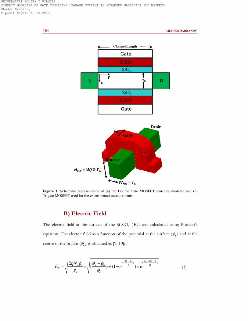
104 GHADER DARBANDY
TSi
x
yy
Channel Length
SiON
SiON
Gate
Gate
SiO2
SiO2
S D
WFIN = TSi
HFIN = W/2-TSi
Source
Drain
GateLg
Figure 1: Schematic representation of (a) the Double Gate MOSFET structure modeled and (b)
Trigate MOSFET used for the experimental measurements.
B) Electric Field
The electric field at the surface of the Si-SiO2 ( SE ) was calculated using Poisson’s
equation. The electric field as a function of the potential at the surface (S
φ ) and at the
centre of the Si film (o
φ ) is obtained as [9, 10]:
2( ) ( )2
( ) (1 )
S O S F
t t
V
a t S OS
s t
qNE e e
φ φ φ φ
φ φφ φ φ
ε φ
− − −−−
= × + − × (1)
UNIVERSITAT ROVIRA I VIRGILI COMPACT MODELING OF GATE TUNNELING LEAKAGE CURRENT IN ADVANCED NANOSCALE SOI MOSFETS Ghader Darbandy Dipòsit Legal: T. 59-2013
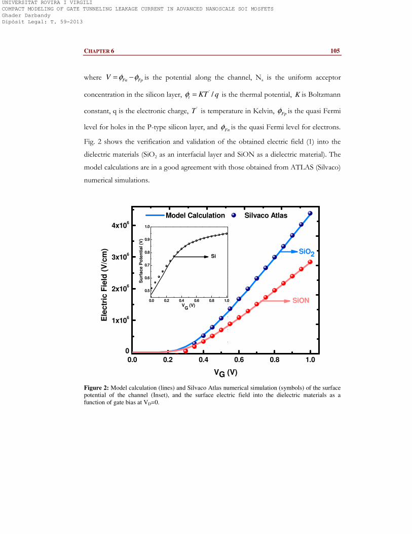
CHAPTER 6 105
where Fn FpV φ φ= − is the potential along the channel, Na is the uniform acceptor
concentration in the silicon layer, ' /t
KT qφ = is the thermal potential, K is Boltzmann
constant, q is the electronic charge, 'T is temperature in Kelvin, Fpφ is the quasi Fermi
level for holes in the P-type silicon layer, and Fn
φ is the quasi Fermi level for electrons.
Fig. 2 shows the verification and validation of the obtained electric field (1) into the
dielectric materials (SiO2 as an interfacial layer and SiON as a dielectric material). The
model calculations are in a good agreement with those obtained from ATLAS (Silvaco)
numerical simulations.
0.0 0.2 0.4 0.6 0.8 1.0
0
1x10⁶
2x10⁶
3x10⁶
4x10⁶
Si
VG
(V)
Su
rfa
ce
Po
ten
tia
l (V
)
0.0 0.2 0.4 0.6 0.8 1.0
0.5
0.6
0.7
0.8
0.9
1.0
SiON
SiO2
Ele
ctr
ic F
ield
(V
/cm
)
VG (V)
Model Calculation Silvaco Atlas
Figure 2: Model calculation (lines) and Silvaco Atlas numerical simulation (symbols) of the surface
potential of the channel (Inset), and the surface electric field into the dielectric materials as a
function of gate bias at VD=0.
UNIVERSITAT ROVIRA I VIRGILI COMPACT MODELING OF GATE TUNNELING LEAKAGE CURRENT IN ADVANCED NANOSCALE SOI MOSFETS Ghader Darbandy Dipòsit Legal: T. 59-2013
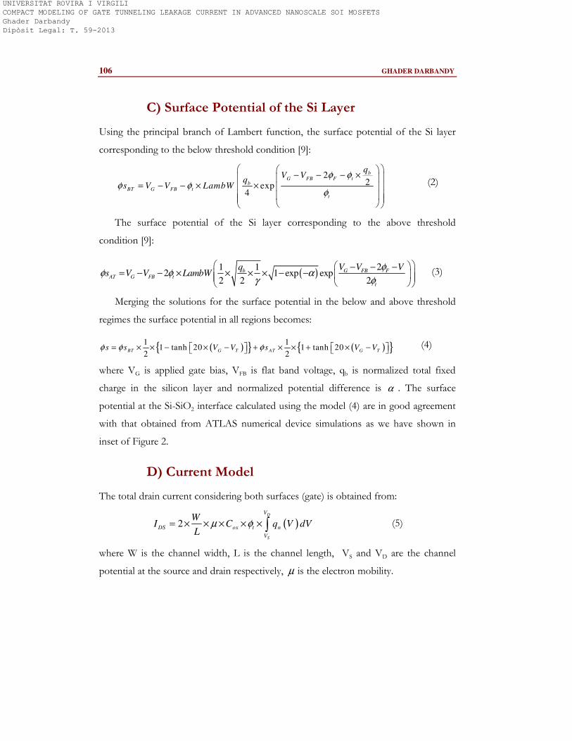
106 GHADER DARBANDY
C) Surface Potential of the Si Layer
Using the principal branch of Lambert function, the surface potential of the Si layer
corresponding to the below threshold condition [9]:
22exp
4
bG FB F t
b
BT G FB t
t
qV V
qs V V LambW
φ φφ φ
φ
− − − ×
= − − × ×
(2)
The surface potential of the Si layer corresponding to the above threshold
condition [9]:
( )21 1
2 1 exp exp2 2 2
b G FB FAT G FB t
t
q V V Vs V V LambW
φφ φ α
γ φ
− − −= − − × × × × − −
(3)
Merging the solutions for the surface potential in the below and above threshold
regimes the surface potential in all regions becomes:
( ){ } ( ){ }1 11 tanh 20 1 tanh 20
2 2BT G T AT G Ts s V V s V Vφ φ φ= × × − × − + × × + × −
(4)
where VG is applied gate bias, VFB is flat band voltage, qb is normalized total fixed
charge in the silicon layer and normalized potential difference is α . The surface
potential at the Si-SiO2 interface calculated using the model (4) are in good agreement
with that obtained from ATLAS numerical device simulations as we have shown in
inset of Figure 2.
D) Current Model
The total drain current considering both surfaces (gate) is obtained from:
( )2D
S
V
DS ox t n
V
WI C q V dV
Lµ φ= × × × × × ∫ (5)
where W is the channel width, L is the channel length, VS and VD are the channel
potential at the source and drain respectively, µ is the electron mobility.
UNIVERSITAT ROVIRA I VIRGILI COMPACT MODELING OF GATE TUNNELING LEAKAGE CURRENT IN ADVANCED NANOSCALE SOI MOSFETS Ghader Darbandy Dipòsit Legal: T. 59-2013
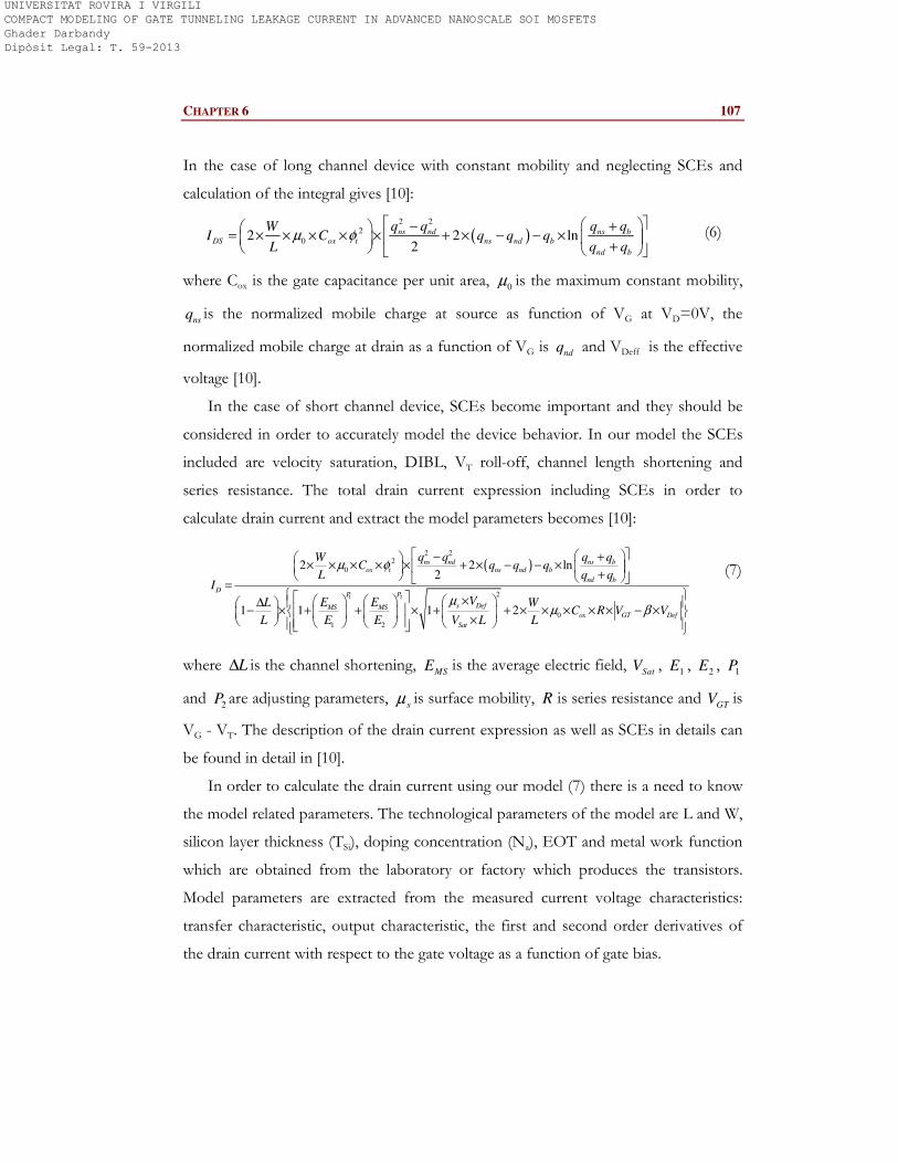
CHAPTER 6 107
In the case of long channel device with constant mobility and neglecting SCEs and
calculation of the integral gives [10]:
( )2 2
2
02 2 ln2
ns nd ns b
DS ox t ns nd b
nd b
q q q qWI C q q q
L q qµ φ
− + = × × × × × + × − − ×
+
(6)
where Cox is the gate capacitance per unit area, 0µ is the maximum constant mobility,
nsq is the normalized mobile charge at source as function of VG at VD=0V, the
normalized mobile charge at drain as a function of VG is ndq and VDeff is the effective
voltage [10].
In the case of short channel device, SCEs become important and they should be
considered in order to accurately model the device behavior. In our model the SCEs
included are velocity saturation, DIBL, VT roll-off, channel length shortening and
series resistance. The total drain current expression including SCEs in order to
calculate drain current and extract the model parameters becomes [10]:
( )
1 2
2 22
0
2
0
1 2
2 2 ln2
1 1 1 2
ns nd ns box t ns nd b
nd b
DP P
s DefMS MSox GT Def
Sat
q q q qWC q q q
L q qI
VE EL WC R V V
L E E V L L
µ φ
µµ β
− + × × × × × + × − − ×
+ = × ∆
− × + + × + + × × × × × − × ×
(7)
where L∆ is the channel shortening, MSE is the average electric field,
SatV , 1E ,
2E , 1P
and 2P are adjusting parameters,
sµ is surface mobility, R is series resistance and GTV is
VG - VT. The description of the drain current expression as well as SCEs in details can
be found in detail in [10].
In order to calculate the drain current using our model (7) there is a need to know
the model related parameters. The technological parameters of the model are L and W,
silicon layer thickness (TSi), doping concentration (Na), EOT and metal work function
which are obtained from the laboratory or factory which produces the transistors.
Model parameters are extracted from the measured current voltage characteristics:
transfer characteristic, output characteristic, the first and second order derivatives of
the drain current with respect to the gate voltage as a function of gate bias.
UNIVERSITAT ROVIRA I VIRGILI COMPACT MODELING OF GATE TUNNELING LEAKAGE CURRENT IN ADVANCED NANOSCALE SOI MOSFETS Ghader Darbandy Dipòsit Legal: T. 59-2013
108 GHADER DARBANDY
3) Model Implementation and Automatic
Parameter Extraction Techniques
Our model is coded in Verilog-A language in order to implement and use automatic
parameter extraction techniques compatible with IC-CAP. It can be used directly in
circuit simulators as well as in parameter extraction software, which provides methods
for handling measured data. The sub-circuit modeling environment, the multiple plot
function and the piped simulation mode is making the quick setup of tests and
measurements followed by automatic parameter extraction routines and easy use for
the new devices when the models have many parameters and parameters have a
complex dependence on fields and voltages.
In order to have a best optimization with the highest accuracy, we have prioritized
the model parameters into the several groups and the extraction procedure begins
from the most important parameters and continues to fix other parameters (less
important ones). At the beginning, parameter extraction will use the initial values (best
guess) as a default value of the parameters, and then the optimization steps will be used
in order to fit simulation to measurements. The improvement of the fitting quality will
be achieved using the optimization steps. Parameter extractions are organized in an
extraction flow and the extraction steps can be selected from available functions in
order to apply direct extractions, optimizers and manual tuners.
4) Results and Discussion
The accuracy of the simulations as using our compact model with the extracted
parameters is verified by comparison with measurements.
UNIVERSITAT ROVIRA I VIRGILI COMPACT MODELING OF GATE TUNNELING LEAKAGE CURRENT IN ADVANCED NANOSCALE SOI MOSFETS Ghader Darbandy Dipòsit Legal: T. 59-2013
CHAPTER 6 109
0.0 0.2 0.4 0.6 0.8 1.0 1.2
0.0
2.0x10⁻⁶
4.0x10⁻⁶
6.0x10⁻⁶
8.0x10⁻⁶
1.0x10⁻⁵
1.2x10⁻⁵
1.4x10⁻⁵
VD =0.05V, T
Si=55nm L
Ch=180nm
LCh
=330nm
LCh
=1u
MeasurementI D
(A
)
VG (V)
0.0 0.2 0.4 0.6 0.8 1.0 1.2
0.0
2.0x10⁻⁵
4.0x10⁻⁵
6.0x10⁻⁵
8.0x10⁻⁵
1.0x10⁻⁴
VD=1V, T
Si=55nm
LCh
=180nm
LCh
=330nm
LCh
=1u
Measurement
I D (
A)
VG (V)
Figure 3: Comparison between simulated drain current as a function of gate bias characteristics after
optimization (using the values of extracted parameters) and measurements at VD=0.05 and VD=1V.
We use the measured transistor characteristics of the Trigate MOSFETs for three
different channel lengths (1000nm, 330nm and 180nm) and two different Si
thicknesses (WFin=55nm and WFin =71nm).
The transfer characteristics were obtained for gate voltage varying from 0 V to 1.2
V, while the drain voltage was fixed at 0.05 V and 1 V for the linear and saturation
regimes respectively. The output characteristics were obtained for different VGS values
in order to verify the abilities of the model and results of transistor simulation.
The surface potential of the channel and surface electric field into the dielectric
materials as a function of gate bias are shown in Figure 2, using our model and
numerical simulation (Silvaco ATLAS) at VD=0. Comparison between our model (7)
calculations and measured data of the drain current for different channel lengths
(Figure 3) and Si thicknesses (Figure 4) are shown at VD=0.05 and VD=1V.
The transconductance (gm) at a particular bias point is the slope of the tangent of
the transfer characteristic curve at that point. We plotted the first derivative of the
drain current with respect to the gate voltage (transconductance) as a function of gate
bias at VD=0.05 and VD=1V for different channel lengths (Figure 5) and Si thickness
(Figure 6).
UNIVERSITAT ROVIRA I VIRGILI COMPACT MODELING OF GATE TUNNELING LEAKAGE CURRENT IN ADVANCED NANOSCALE SOI MOSFETS Ghader Darbandy Dipòsit Legal: T. 59-2013
110 GHADER DARBANDY
0.0 0.2 0.4 0.6 0.8 1.0 1.2
0.0
5.0x10⁻⁶
1.0x10⁻⁵
1.5x10⁻⁵
2.0x10⁻⁵
LCh
=180nm, VD =0.05V
TSi=71nm
TSi=55nm
I D (
A)
VG (V)
Measurement
0.0 0.2 0.4 0.6 0.8 1.0 1.2
0.0
2.0x10⁻⁵
4.0x10⁻⁵
6.0x10⁻⁵
8.0x10⁻⁵
1.0x10⁻⁴
1.2x10⁻⁴
LCh
=180nm, VD=1V
TSi=71nm
TSi=55nm
I D (
A)
VG (V)
Measurement
Figure 4: Comparison between simulated ID-VG characteristics (symbols) and measurements (lines)
for our model with extracted parameters at VD=0.05 and VD=1V for different Si thickness.
0.0 0.2 0.4 0.6 0.8 1.0 1.2
0.0
5.0x10⁻⁶
1.0x10⁻⁵
1.5x10⁻⁵
2.0x10⁻⁵
2.5x10⁻⁵
VD=0.05V, T
Si=55nm
LCh
=180nm
LCh
=330nm
LCh
=1u
Measurement
gm
1 (
A/V
)
VG (V)
0.0 0.2 0.4 0.6 0.8 1.0 1.2
0.0
5.0x10⁻⁵
1.0x10⁻⁴
1.5x10⁻⁴
VD=1V, T
Si=71nm
MeasurementL
Ch=180nm
LCh
=330nm
LCh
=1u
gm
1 (
A/V
)
VG (V)
Figure 5: Modeled and experimental first derivative of I/V (transconductance) for different channel
lengths at VD=0.05 and VD=1 V.
The second order derivatives of the drain current with respect to the gate voltage
(gm2) are analyzed as a function of gate bias for different channel lengths (Figure 7)
and Si thicknesses (Figure 8) at VD=0.05 and VD=1V. Continuity of the second
derivative of the drain current is obtained as shown in Figure 7 and Figure 8. A lack of
continuity of the second derivative could originate convergence problems of the model
when used in circuit simulation.
UNIVERSITAT ROVIRA I VIRGILI COMPACT MODELING OF GATE TUNNELING LEAKAGE CURRENT IN ADVANCED NANOSCALE SOI MOSFETS Ghader Darbandy Dipòsit Legal: T. 59-2013
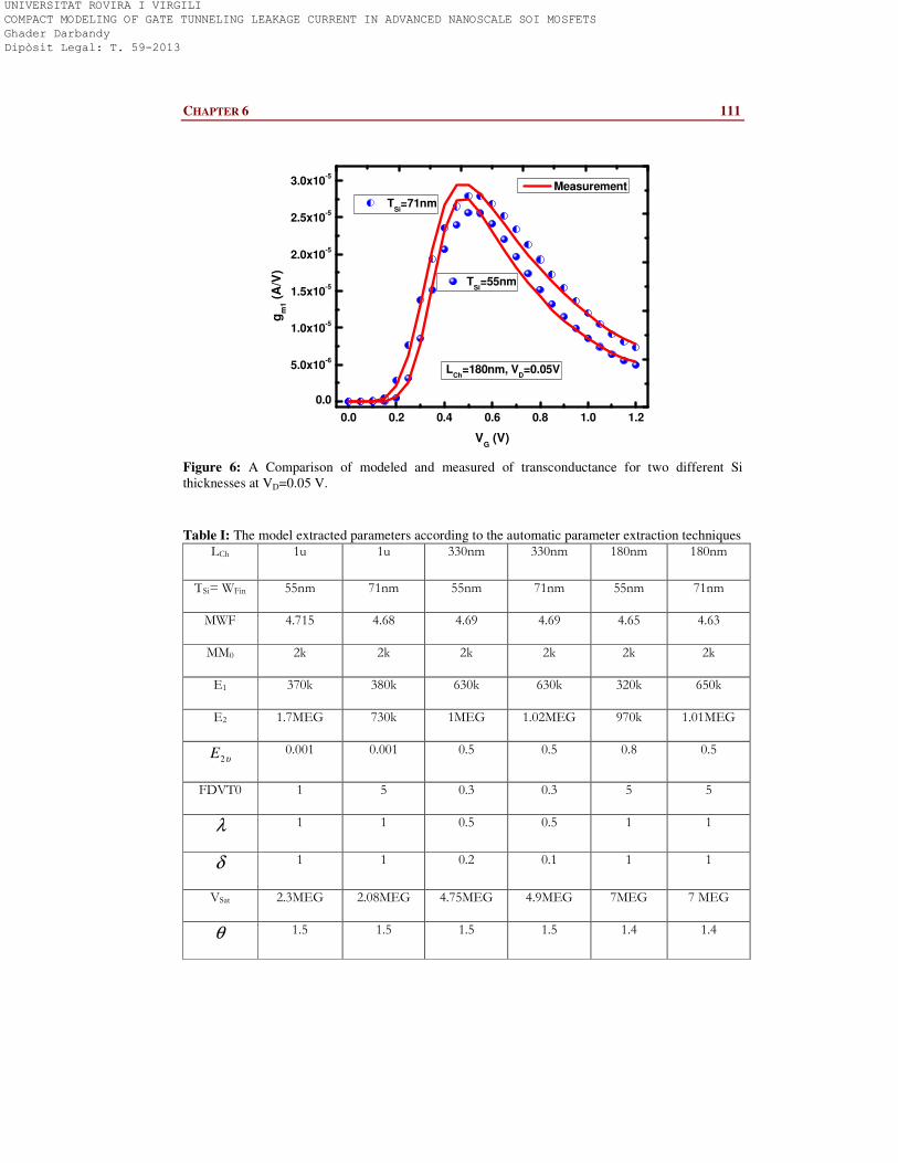
CHAPTER 6 111
0.0 0.2 0.4 0.6 0.8 1.0 1.2
0.0
5.0x10⁻⁶
1.0x10⁻⁵
1.5x10⁻⁵
2.0x10⁻⁵
2.5x10⁻⁵
3.0x10⁻⁵
LCh
=180nm, VD=0.05V
TSi=71nm
TSi
=55nmg
m1 (
A/V
)
VG (V)
Measurement
Figure 6: A Comparison of modeled and measured of transconductance for two different Si
thicknesses at VD=0.05 V.
Table I: The model extracted parameters according to the automatic parameter extraction techniques
LCh 1u 1u 330nm 330nm 180nm 180nm
TSi= WFin 55nm 71nm 55nm 71nm 55nm 71nm
MWF 4.715 4.68 4.69 4.69 4.65 4.63
MM0 2k 2k 2k 2k 2k 2k
E1 370k 380k 630k 630k 320k 650k
E2 1.7MEG 730k 1MEG 1.02MEG 970k 1.01MEG
2E υ 0.001 0.001 0.5 0.5 0.8 0.5
FDVT0 1 5 0.3 0.3 5 5
λ 1 1 0.5 0.5 1 1
δ 1 1 0.2 0.1 1 1
VSat 2.3MEG 2.08MEG 4.75MEG 4.9MEG 7MEG 7 MEG
θ 1.5 1.5 1.5 1.5 1.4 1.4
UNIVERSITAT ROVIRA I VIRGILI COMPACT MODELING OF GATE TUNNELING LEAKAGE CURRENT IN ADVANCED NANOSCALE SOI MOSFETS Ghader Darbandy Dipòsit Legal: T. 59-2013
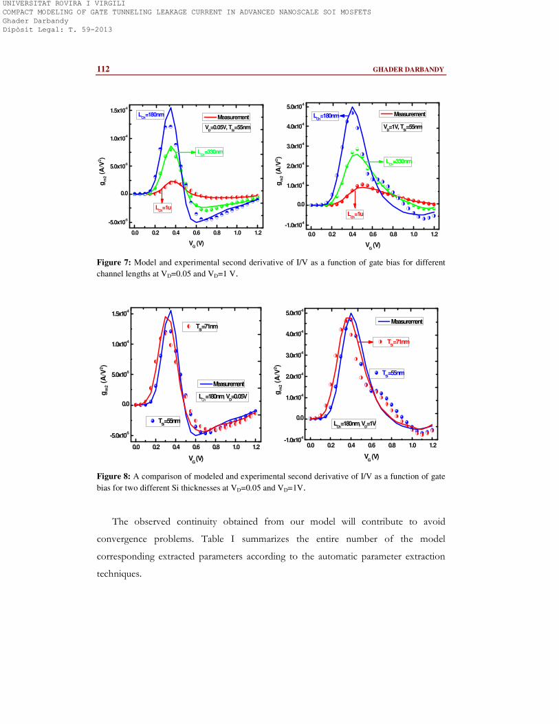
112 GHADER DARBANDY
0.0 0.2 0.4 0.6 0.8 1.0 1.2
-5.0x10⁻⁵
0.0
5.0x10⁻⁵
1.0x10⁻⁴
1.5x10⁻⁴
VD=0.05V, T
Si=55nm
LCh
=180nm
LCh
=330nm
LCh
=1u
Measurement
gm
2 (
A/V
2)
VG (V)
0.0 0.2 0.4 0.6 0.8 1.0 1.2
-1.0x10⁻⁴
0.0
1.0x10⁻⁴
2.0x10⁻⁴
3.0x10⁻⁴
4.0x10⁻⁴
5.0x10⁻⁴
VD=1V, T
Si=55nm
LCh
=180nm
LCh
=330nm
LCh
=1u
Measurement
gm
2 (
A/V
2)
VG (V)
Figure 7: Model and experimental second derivative of I/V as a function of gate bias for different
channel lengths at VD=0.05 and VD=1 V.
0.0 0.2 0.4 0.6 0.8 1.0 1.2
-5.0x10⁻⁵
0.0
5.0x10⁻⁵
1.0x10⁻⁴
1.5x10⁻⁴
LCh
=180nm, VD=0.05V
TSi=71nm
TSi=55nm
gm
2 (
A/V
2)
VG (V)
Measurement
0.0 0.2 0.4 0.6 0.8 1.0 1.2-1.0x10
-4
0.0
1.0x10⁻⁴
2.0x10⁻⁴
3.0x10⁻⁴
4.0x10⁻⁴
5.0x10⁻⁴
LCh
=180nm, VD=1V
TSi=71nm
TSi=55nm
gm
2 (
A/V
2)
VG (V)
Measurement
Figure 8: A comparison of modeled and experimental second derivative of I/V as a function of gate
bias for two different Si thicknesses at VD=0.05 and VD=1V.
The observed continuity obtained from our model will contribute to avoid
convergence problems. Table I summarizes the entire number of the model
corresponding extracted parameters according to the automatic parameter extraction
techniques.
UNIVERSITAT ROVIRA I VIRGILI COMPACT MODELING OF GATE TUNNELING LEAKAGE CURRENT IN ADVANCED NANOSCALE SOI MOSFETS Ghader Darbandy Dipòsit Legal: T. 59-2013
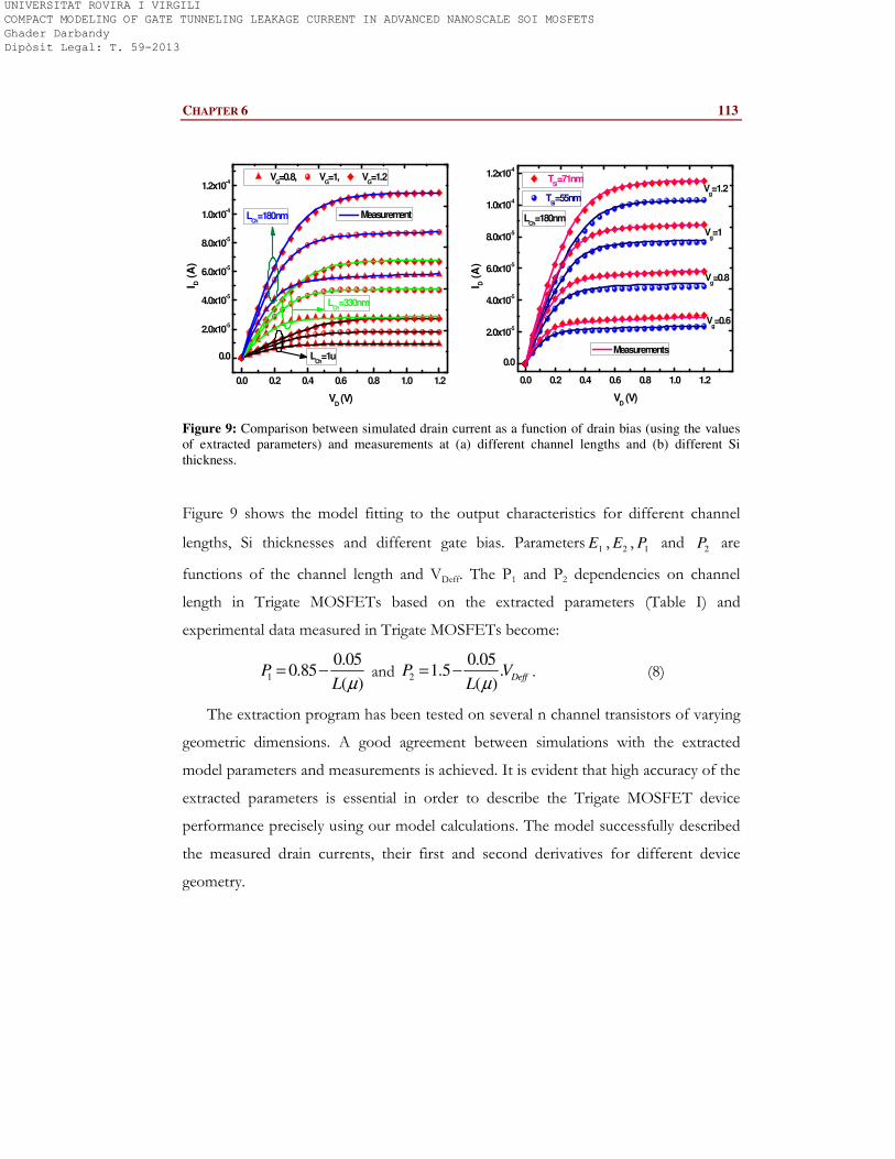
CHAPTER 6 113
0.0 0.2 0.4 0.6 0.8 1.0 1.2
0.0
2.0x10⁻⁵
4.0x10⁻⁵
6.0x10⁻⁵
8.0x10⁻⁵
1.0x10⁻⁴
1.2x10⁻⁴
LCh
=1u
LCh
=330nm
LCh
=180nm Measurement
VG=0.8, V
G=1, V
G=1.2
I D (
A)
VD (V)
0.0 0.2 0.4 0.6 0.8 1.0 1.2
0.0
2.0x10⁻⁵
4.0x10⁻⁵
6.0x10⁻⁵
8.0x10⁻⁵
1.0x10⁻⁴
1.2x10⁻⁴
Vg=0.6
TSi=71nm
TSi=55nm
Measurements
Vg=0.8
Vg=1
Vg=1.2
LCh
=180nm
I D (
A)
VD (V)
Figure 9: Comparison between simulated drain current as a function of drain bias (using the values
of extracted parameters) and measurements at (a) different channel lengths and (b) different Si
thickness.
Figure 9 shows the model fitting to the output characteristics for different channel
lengths, Si thicknesses and different gate bias. Parameters1E ,
2E ,1P and
2P are
functions of the channel length and VDeff. The P1 and P2 dependencies on channel
length in Trigate MOSFETs based on the extracted parameters (Table I) and
experimental data measured in Trigate MOSFETs become:
1
0.050.85
( )P
L µ= − and 2
0.051.5 .
( )DeffP V
L µ= − . (8)
The extraction program has been tested on several n channel transistors of varying
geometric dimensions. A good agreement between simulations with the extracted
model parameters and measurements is achieved. It is evident that high accuracy of the
extracted parameters is essential in order to describe the Trigate MOSFET device
performance precisely using our model calculations. The model successfully described
the measured drain currents, their first and second derivatives for different device
geometry.
UNIVERSITAT ROVIRA I VIRGILI COMPACT MODELING OF GATE TUNNELING LEAKAGE CURRENT IN ADVANCED NANOSCALE SOI MOSFETS Ghader Darbandy Dipòsit Legal: T. 59-2013
114 GHADER DARBANDY
5) Conclusion
We have developed automatic parameter extraction techniques for our explicit
compact model in DG MOSFET suitable for design and circuits simulation, based on
a surface potential model including short channel effects (channel length modulation,
DIBL, carrier velocity saturation, threshold voltage roll-off and series resistance). The
P1 and P2 parameters dependencies on the channel length are investigated and shown
for Trigate MOSFETs based on measured data and extracted parameters. The
continuity of the second derivative of the drain current with respect to the gate bias is
verified and evaluated by plotting the derivatives at different conditions. The simulated
I-V characteristics in linear and saturation regions and the first and second derivatives
of the drain current using the extracted parameters show good agreement in all
operating regions when compared to available measured data for Trigate MOSFETs
with different geometry size.
References
[1] Y. Mahotin and E. Lyumkis, “Automatic BSIM3/4 Model Parameter Extraction
with Penalty Function”, NSTI-Nanotech 2004, Vol. 2, ISBN 0-9728422-8-4
[2] N. Chevillon, M. Tang, F. Pregaldiny, C. Lallement and M. Madec, "FinFET
Compact Modelling and parameter extraction", Proc. 16th Int. Conf. Mixed Design of
Integrated Circuits and Systems (MIXDES'09)
[3] Joaquın Alvarado1, Benjamin Iniguez, Magali Estrada, Denis Flandre and Antonio
Cerdeira, “Implementation of the symmetric doped double-gate MOSFET model in
Verilog-A for circuit simulation”, Int. J. Numer. Model, 2010; 23:88–106.
[4] Darsen Duane Lu, “Compact Models for Future Generation CMOS”, Ph.D
Dissetration, University of California, Berkeley, 2011.
[5] Chung-Hsun Lin, “Compact Modeling of Nanoscale CMOS”, Ph.D Dissetration,
University of California, Berkeley, 2007
UNIVERSITAT ROVIRA I VIRGILI COMPACT MODELING OF GATE TUNNELING LEAKAGE CURRENT IN ADVANCED NANOSCALE SOI MOSFETS Ghader Darbandy Dipòsit Legal: T. 59-2013
CHAPTER 6 115
[6] Masaki Kondo, Hidetoshi Onodera, Member, and Keikichi Tamaru, “Model-
Adaptable MOSFET Parameter-Extraction Method Using an Intermediate Model”,
IEEE Transaction on computer aided design of integrated circuits and systems, VOL. 17, NO. 5,
1998
[7] P. R. Karlsson and K. O. Jeppson, “An Analytical Strategy for Fast Extraction of
MOS Transistor DC Parameters Applied to the SPICE MOS3 and BSIM Models”,
Proc. IEEE Int. Conference on Microelectronic Test Structures, Vol 5 (1992)
[8] Device simulator ATLAS, Silvaco International, available from
http://www.silvaco.com.
[9] A. Cerdeira, O. Moldovan, B. Iñiguez and M. Estrada, “Modeling of potentials and
threshold voltage for symmetric doped double-gate MOSFETs”, Solid-State Electronics,
vol. 52, no. 5, pp. 830-837, May 2008
[10] A. Cerdeira, B. Iñiguez and M. Estrada, “Compact model for short channel
symmetric doped double-gate MOSFET”, Solid-State Electronics, vol. 52, no. 7, pp. 1064-
1070, July 2008
[11] Geoffrey J. Coram “How to (and how not to) Write a Compact Model in Verilog-
A” Proc. 2004 IEEE International Behavioral Modeling and Simulation Conference (BMAS
2004)
[12] Verilog-AMS Language Reference Manual, version 2.2, Accellera, 2004.
[13] K.S. Kundert and O. Zinke, The Designer’s Guide to Verilog-AMS, Boston: Kluver
Academic Publishers (2004).
UNIVERSITAT ROVIRA I VIRGILI COMPACT MODELING OF GATE TUNNELING LEAKAGE CURRENT IN ADVANCED NANOSCALE SOI MOSFETS Ghader Darbandy Dipòsit Legal: T. 59-2013

116 GHADER DARBANDY
UNIVERSITAT ROVIRA I VIRGILI COMPACT MODELING OF GATE TUNNELING LEAKAGE CURRENT IN ADVANCED NANOSCALE SOI MOSFETS Ghader Darbandy Dipòsit Legal: T. 59-2013
117
Chapter 7
Automatic Parameter Extraction Techniques and
Parameters Correlations of Gate Leakage Current Model
in Double-Gate MOSFETs, with IC-CAP
Direct Tunneling (DT) and Trap Assisted Tunneling (TAT) gate leakage current
parameters have been extracted and verified considering automatic parameter
extraction approaches. The commercial package IC-CAP is used to simulate our
leakage current model coded in Verilog-A, and comparing with the measurements in
order to obtain model parameter values and study parameters correlations. The model
and parameter extraction techniques have been used to study the impact of parameters
in the gate leakage current based on our developed compact analytical model and
experimental data. It is shown that the gate leakage current depends on interfacial
barrier height more strongly than barrier height of the dielectric layer. There is almost
same scenario with respect to the carrier effective masses into the interfacial layer and
dielectric layer. The comparison of the simulated results shows good agreement with
available gate leakage current measured transistor characteristic in Trigate MOSFET.
UNIVERSITAT ROVIRA I VIRGILI COMPACT MODELING OF GATE TUNNELING LEAKAGE CURRENT IN ADVANCED NANOSCALE SOI MOSFETS Ghader Darbandy Dipòsit Legal: T. 59-2013
118 GHADER DARBANDY
1) Introduction
With the downscaling of CMOS technologies, many MOSFET models have been
developed in order to accurately describe gate leakage current and new physical
phenomena in the device behavior [1-3]. Accurate model expressions are necessary to
achieve the correct physical and real device/circuit behavior. Additionally, high precise
parameter extraction is another important aspect of device and circuit simulation to
ensure that the extracted parameters are an accurate reflection of the effects and
performances [4-7]. Automatic parameter extraction techniques are an alternative to
optimize the model parameters for the determination of model parameter values in
comparison with measured data [8].
The commercial parameter extraction package (IC-CAP) is used to apply automatic
parameter extraction techniques and simulating our gate leakage current models which
is coded in Verilog-A. IC-CAP provides extraction routines for industry standard and
supports the use of models in Verilog-A and wide range of customer requirements. IC-
CAP uses different optimization algorithms and combination of those algorithms can
be a main advantage of parameter extraction [9, 10]. Parameter extractions are
organized in an extraction flow and extraction steps can be selected from available
functions in order to apply direct extraction, optimizers and manual tuners.
In this work we have applied compact analytical gate leakage current models in the
DT regime and TAT regime for the prediction of gate leakage current. We have
developed and implemented automatic parameter extraction strategies for DT and
TAT current models in the available parameter extraction system (IC-CAP). These
techniques have been applied to the gate leakage current measurements in Trigate
MOSFET and have given successfully results. We have shown parameters correlations
based on our developed gate leakage current models, automatic parameter extraction
techniques and measured gate leakage current data in Trigate MOSFET.
UNIVERSITAT ROVIRA I VIRGILI COMPACT MODELING OF GATE TUNNELING LEAKAGE CURRENT IN ADVANCED NANOSCALE SOI MOSFETS Ghader Darbandy Dipòsit Legal: T. 59-2013
CHAPTER 7 119
The analyzed correlations of parameters provide knowledge of the sensitivity of the
model parameters and an insight into the gate leakage current model available for
circuit simulation. Comparison between simulated leakage current (using related
extracted model parameters) show good agreement with the gate leakage current
measurements in Trigate MOSFET with different geometries.
2) Device Structure and Gate Leakage Current
Models
Figure 1 shows structure of the device under analysis which it is modeled as DG
MOSFETs, as well as Trigate MOSFET structure which the gate leakage current
measurements carried out. The DT and TAT current mechanisms have been
developed and implemented in Verilog-A code for accurate simulation of the gate
leakage current through two layer gate oxide materials (SiON/SiO2 stack). The gate
leakage current is calculated based on the proper tunneling probabilities through two
layers gate oxide material such as SiON/SiO2 with EOT=1.9nm. To achieve good
performance we need to have accurate models and find techniques to extract model
parameter values with high accuracy. The extraction techniques are based on the
measurements and our developed model equations (4, 10) to ensure that a good
representation of the device characteristics will be achieved.
A) Structure
The gate leakage current measurements carried out on Trigate MOSFET (Fig 1b) with
TSiO2=1nm, TSiON=1.4nm (EOT=1.9nm), channel length equal to 1µm and 10 µm,
HFin=65nm and WFin=55nm through SiON/SiO2 gate oxide materials in terms of gate
bias. The TAT current is dominant in subthreshold regime while above threshold
voltage the DT is dominant and TAT is negligible [11].
UNIVERSITAT ROVIRA I VIRGILI COMPACT MODELING OF GATE TUNNELING LEAKAGE CURRENT IN ADVANCED NANOSCALE SOI MOSFETS Ghader Darbandy Dipòsit Legal: T. 59-2013
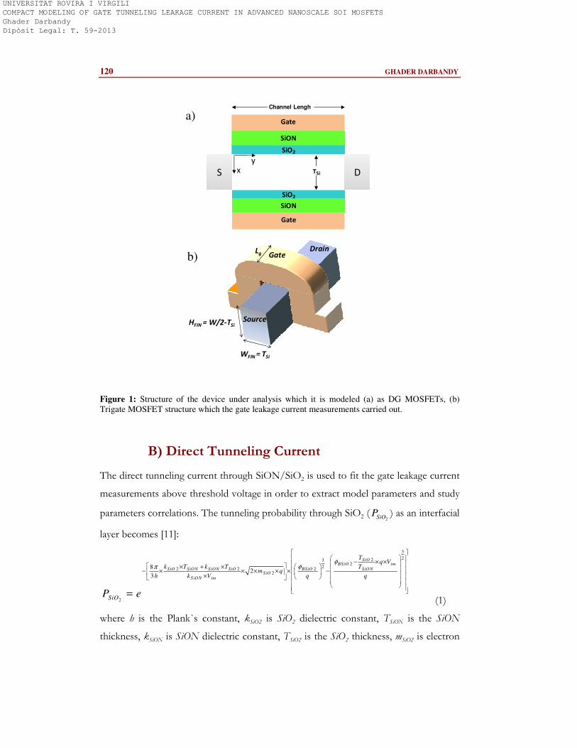
120 GHADER DARBANDY
Gate
y
Dx
Channel Lengh
TSiS
SiON
SiO2
SiO2
SiON
Gate
WFIN = TSi
HFIN = W/2-TSiSource
DrainGate
Lg
a)
b)
Figure 1: Structure of the device under analysis which it is modeled (a) as DG MOSFETs, (b)
Trigate MOSFET structure which the gate leakage current measurements carried out.
B) Direct Tunneling Current
The direct tunneling current through SiON/SiO2 is used to fit the gate leakage current
measurements above threshold voltage in order to extract model parameters and study
parameters correlations. The tunneling probability through SiO2 (2SiOP ) as an interfacial
layer becomes [11]:
3
2232
22 2 2
2
2
82
3
SiOBSiO im
SiO SiON SiON SiO BSiO SiONSiO
SiON im
Tq V
k T k T Tm q
h k V q q
SiOP e
φφπ
− × × × + × − × × × × × − × =
(1)
where h is the Plank`s constant, kSiO2 is SiO2 dielectric constant, TSiON is the SiON
thickness, kSiON is SiON dielectric constant, TSiO2 is the SiO2 thickness, mSiO2 is electron
UNIVERSITAT ROVIRA I VIRGILI COMPACT MODELING OF GATE TUNNELING LEAKAGE CURRENT IN ADVANCED NANOSCALE SOI MOSFETS Ghader Darbandy Dipòsit Legal: T. 59-2013
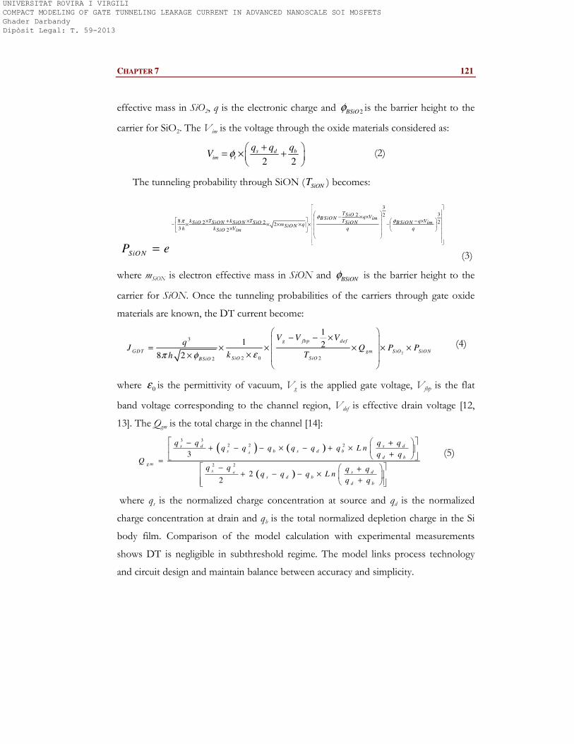
CHAPTER 7 121
effective mass in SiO2, q is the electronic charge and 2BSiOφ is the barrier height to the
carrier for SiO2. The Vim is the voltage through the oxide materials considered as:
2 2
s d bim t
q q qV φ
+ = × +
(2)
The tunneling probability through SiON ( SiONT ) becomes:
3
32 28 22 2 23 2
TSiO q VBSiON imk T k T T q VSiO SiON SiON SiO SiON BSiON imm qSiON
h k V q qSiO im
SiONP e
φφπ
− × × × + × − × − × × × × × − ×
= (3)
where mSiON is electron effective mass in SiON and BSiON
φ is the barrier height to the
carrier for SiON. Once the tunneling probabilities of the carriers through gate oxide
materials are known, the DT current become:
2
3
2 0 22
11 2
8 2
g fbp def
GDT gm SiO SiON
SiO SiOBSiO
V V Vq
J Q P Pk Th επ φ
− − ×
= × × × × × ××
(4)
where 0ε is the permittivity of vacuum, Vg is the applied gate voltage, Vfbp is the flat
band voltage corresponding to the channel region, Vdef is effective drain voltage [12,
13]. The Qgm is the total charge in the channel [14]:
( ) ( )
( )
3 32 2 2
2 2
3
22
d
d
s d s ds b s d b
d b
g m
s s ds d b
d b
q q q qq q q q q q L n
q qQ
q q q qq q q L n
q q
− ++ − − × − + ×
+ = − +
+ − − × +
(5)
where qs is the normalized charge concentration at source and qd is the normalized
charge concentration at drain and qb is the total normalized depletion charge in the Si
body film. Comparison of the model calculation with experimental measurements
shows DT is negligible in subthreshold regime. The model links process technology
and circuit design and maintain balance between accuracy and simplicity.
UNIVERSITAT ROVIRA I VIRGILI COMPACT MODELING OF GATE TUNNELING LEAKAGE CURRENT IN ADVANCED NANOSCALE SOI MOSFETS Ghader Darbandy Dipòsit Legal: T. 59-2013
122 GHADER DARBANDY
C) Trap Assisted Tunneling Current
The TAT current is becoming important and dominated in subthreshold regime where
the DT is negligible. The proper tunneling probabilities through SiO2 corresponding to
the Source/Drain side`s cannel overlap (2 /SiO S D
PTAT ) become:
3
2232 /
22 2 2
2/
2
82
3
/
SiOBSiO IappGS GD
SiO SiON SiON SiO BSiO SiONSiO
SiON IappGS GD
Tq V
k T k T Tm q
h k V q q
SiO S DPTAT e
φφπ
− × × × + × − × × × × × − × =
(6)
where / /IappGS GD g FBn S DV V V V= − − . The proper tunneling probabilities through SiON
corresponding to the Source/Drain side`s cannel overlap ( /SiONS DPTAT ) become:
( )
( )
3
2
1
/ 2
82
3
/
SiO N Trap
IappG S G D SiO SiO N
q mh
V T T
SiO N S DPTAT e
πφ
−
× × × × + = (7)
where Trapφ is the trap energy. Using the considered tunneling probabilities through
SiON/SiO2, the TAT current corresponding to the source/drain side`s cannel overlap
become:
( ) 2/ / /14
/ 2
2
3 10
Trap Trap Trap
GTATS D SiO S D SiONS D
IappGS GD SiO SiON
C N qJ PTAT PTAT
V T T
φ−
× × × × = × × × × × +
(8)
where NTrap is the trap states density and
532
0
3
1 6
3
e
T rap
S iO N T rap e
mC
m h
π φ
φ φ
= × −
(9)
where eφ is the total energy of electrons considered equal to 0.2 (eV). The total TAT
current ( GTATTOTJ ) corresponding to the both sides of source and drain channel overlap
become:
G T A T T O T G T A T S G T A T DJ J J= +
(10)
We have implemented the developed DT and TAT current in automatic parameter
extraction techniques using Verilog-A language in commercial IC-CAP package.
UNIVERSITAT ROVIRA I VIRGILI COMPACT MODELING OF GATE TUNNELING LEAKAGE CURRENT IN ADVANCED NANOSCALE SOI MOSFETS Ghader Darbandy Dipòsit Legal: T. 59-2013
CHAPTER 7 123
3) Model Implementation in Verilog-A and
Parameter Extraction inside IC-CAP
The implementation of the developed DT and TAT compact model is presented in
Verilog-A code which is simulated in IC-CAP as a commercial package for parameter
extraction. Verification of the extracted parameters and parameters correlations is
performed against the gate leakage current measurements in Trigate MOSFET. The
gate leakage current models are coded in verilog-A which makes it applicable to other
simulators and industry IC design tools.
We present experimental study of the gate leakage tunneling current parameters
correlations in Trigate MOSFET. In order to show the correlation between two
parameters we have fixed one of the parameters in different values and we have tried
to extract the other parameter by fitting simulated leakage current with those obtained
from measurements.
4) Experimental Results and Discussion
The extraction techniques have been applied on n channel Trigate MOSFET with
SiON/SiO2 as gate dielectric stacks. Comparison of the simulation calculations to the
measured data of the gate leakage current on Trigate MOSFETs allows obtaining DT
and TAT current parameter values. Automatic parameter extraction techniques have
been used to extract the model parameters and to illustrate parameters correlations for
two sample device geometries. In the automatic parameter extraction routines a set of
gate leakage current as a function of gate bias is used for each transistor and then
optimizations are performed for the parameters in different group based on their
important and priorities.
Table I, lists the corresponding parameter values of the TAT current and DT
current based on experimental measurements. Figure 2 shows a good agreement
between simulated plots from the application of DT (4) model and TAT (10) model
using the extracted parameters (Table I) and measured data.
UNIVERSITAT ROVIRA I VIRGILI COMPACT MODELING OF GATE TUNNELING LEAKAGE CURRENT IN ADVANCED NANOSCALE SOI MOSFETS Ghader Darbandy Dipòsit Legal: T. 59-2013
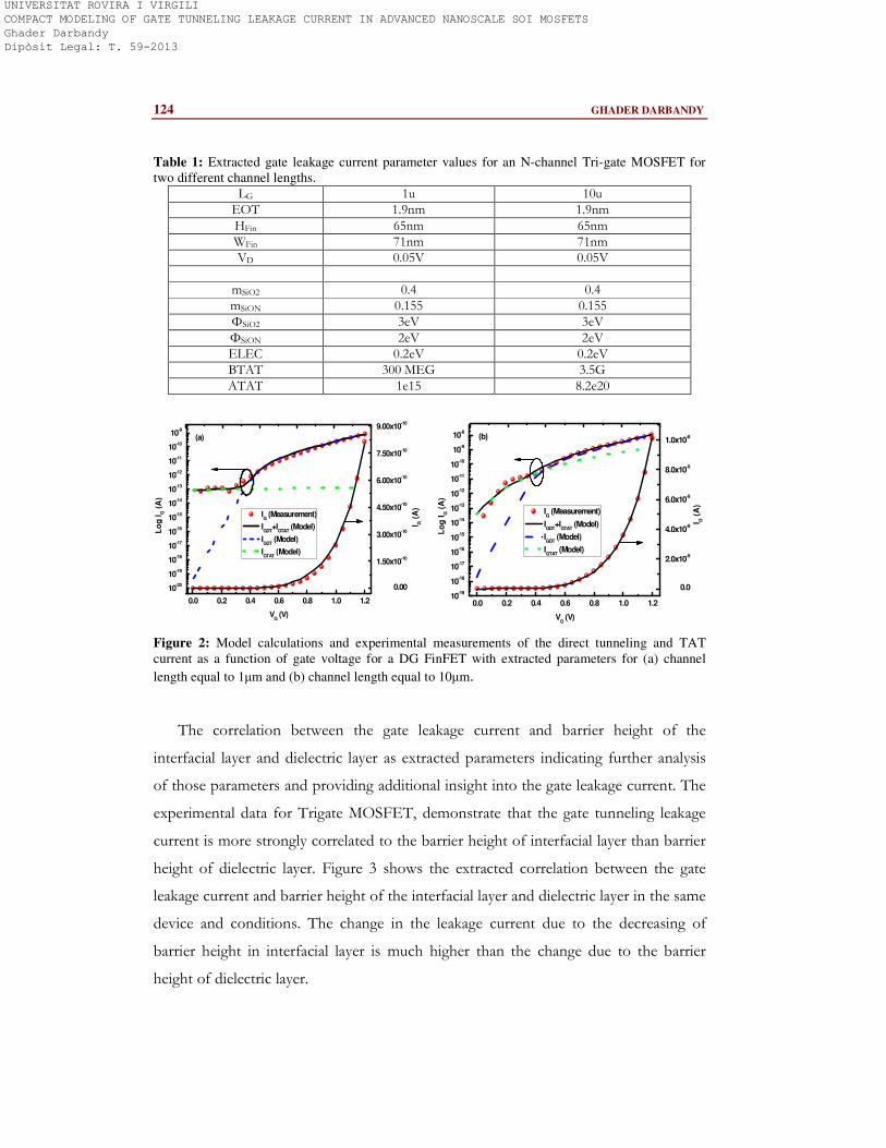
124 GHADER DARBANDY
Table 1: Extracted gate leakage current parameter values for an N-channel Tri-gate MOSFET for
two different channel lengths.
LG 1u 10u EOT 1.9nm 1.9nm HFin 65nm 65nm WFin 71nm 71nm VD 0.05V 0.05V
mSiO2 0.4 0.4 mSiON 0.155 0.155 ΦSiO2 3eV 3eV ΦSiON 2eV 2eV ELEC 0.2eV 0.2eV BTAT 300 MEG 3.5G ATAT 1e15 8.2e20
0.0 0.2 0.4 0.6 0.8 1.0 1.2
0.00
1.50x10⁻¹⁰
3.00x10⁻¹⁰
4.50x10⁻¹⁰
6.00x10⁻¹⁰
7.50x10⁻¹⁰
9.00x10⁻¹⁰
10-20
10-19
10-18
10-17
10-16
10-15
10-14
10-13
10-12
10-11
10-10
10-9
VG (V)
I G (
A)
Lo
g I
G (
A)
IG (Measurement)
IGDT
+IGTAT
(Model)
IGDT
(Model)
IGTAT
(Model)
(a)
0.0 0.2 0.4 0.6 0.8 1.0 1.2
0.0
2.0x10⁻⁹
4.0x10⁻⁹
6.0x10⁻⁹
8.0x10⁻⁹
1.0x10⁻⁸
10-19
10-18
10-17
10-16
10-15
10-14
10-13
10-12
10-11
10-10
10-9
10-8
V
G (V)
I G (
A)
Lo
g I
G (
A)
IG (Measurement)
IGDT
+IGTAT
(Model)
IGDT
(Model)
IGTAT
(Model)
(b)
Figure 2: Model calculations and experimental measurements of the direct tunneling and TAT
current as a function of gate voltage for a DG FinFET with extracted parameters for (a) channel
length equal to 1µm and (b) channel length equal to 10µm.
The correlation between the gate leakage current and barrier height of the
interfacial layer and dielectric layer as extracted parameters indicating further analysis
of those parameters and providing additional insight into the gate leakage current. The
experimental data for Trigate MOSFET, demonstrate that the gate tunneling leakage
current is more strongly correlated to the barrier height of interfacial layer than barrier
height of dielectric layer. Figure 3 shows the extracted correlation between the gate
leakage current and barrier height of the interfacial layer and dielectric layer in the same
device and conditions. The change in the leakage current due to the decreasing of
barrier height in interfacial layer is much higher than the change due to the barrier
height of dielectric layer.
UNIVERSITAT ROVIRA I VIRGILI COMPACT MODELING OF GATE TUNNELING LEAKAGE CURRENT IN ADVANCED NANOSCALE SOI MOSFETS Ghader Darbandy Dipòsit Legal: T. 59-2013
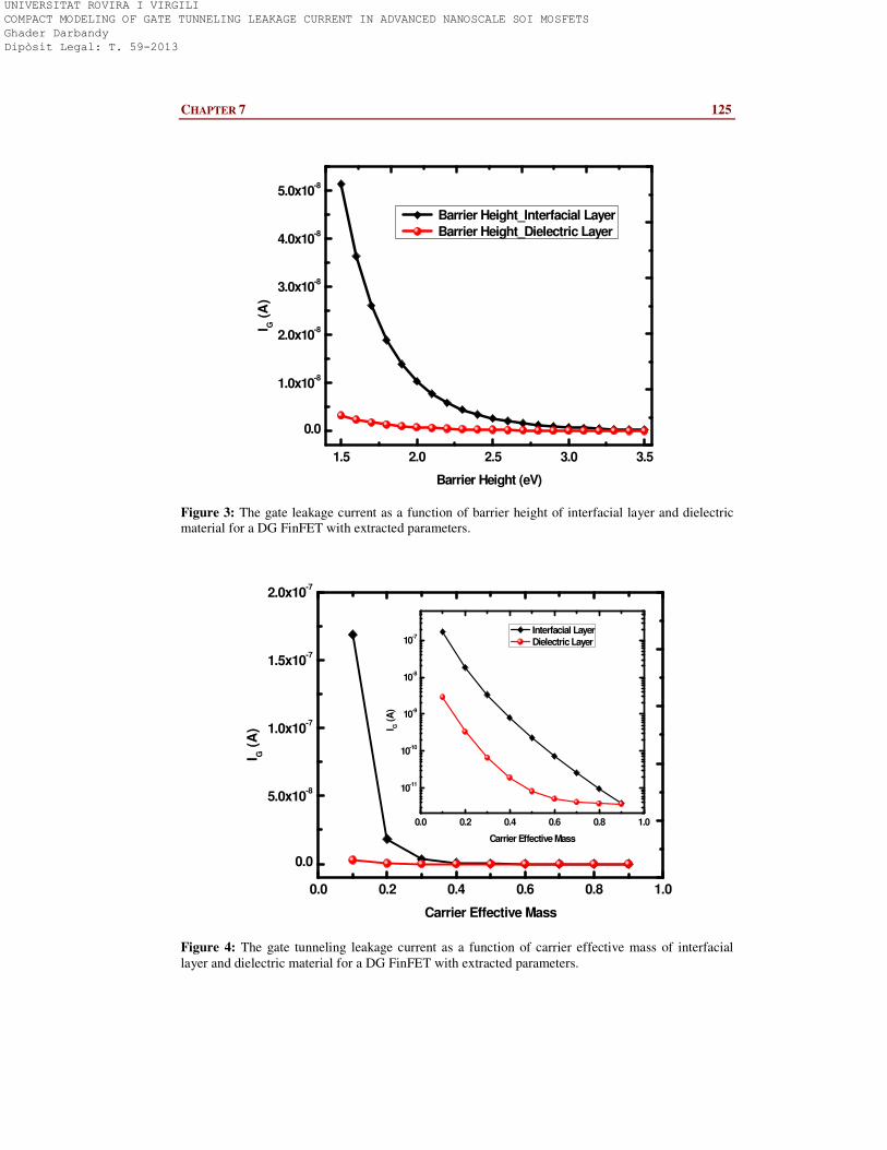
CHAPTER 7 125
1.5 2.0 2.5 3.0 3.5
0.0
1.0x10⁻⁸
2.0x10⁻⁸
3.0x10⁻⁸
4.0x10⁻⁸
5.0x10⁻⁸
I G (
A)
Barrier Height (eV)
Barrier Height_Interfacial Layer
Barrier Height_Dielectric Layer
Figure 3: The gate leakage current as a function of barrier height of interfacial layer and dielectric
material for a DG FinFET with extracted parameters.
0.0 0.2 0.4 0.6 0.8 1.0
0.0
5.0x10⁻⁸
1.0x10⁻⁷
1.5x10⁻⁷
2.0x10⁻⁷
I G (
A)
Carrier Effective Mass
0.0 0.2 0.4 0.6 0.8 1.0
10-11
10-10
10-9
10-8
10-7
I G (A
)
Carrier Effective Mass
Interfacial Layer
Dielectric Layer
Figure 4: The gate tunneling leakage current as a function of carrier effective mass of interfacial
layer and dielectric material for a DG FinFET with extracted parameters.
UNIVERSITAT ROVIRA I VIRGILI COMPACT MODELING OF GATE TUNNELING LEAKAGE CURRENT IN ADVANCED NANOSCALE SOI MOSFETS Ghader Darbandy Dipòsit Legal: T. 59-2013
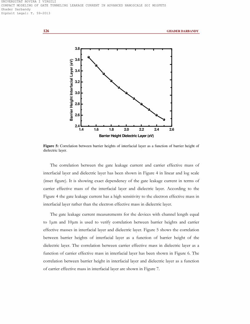
126 GHADER DARBANDY
1.4 1.6 1.8 2.0 2.2 2.4 2.62.4
2.6
2.8
3.0
3.2
3.4
3.6
3.8
Ba
rrie
r H
eig
ht
Inte
rfa
cia
l L
ay
er
(eV
)
Barrier Height Dielectric Layer (eV)
Figure 5: Correlation between barrier heights of interfacial layer as a function of barrier height of
dielectric layer.
The correlation between the gate leakage current and carrier effective mass of
interfacial layer and dielectric layer has been shown in Figure 4 in linear and log scale
(inset figure). It is showing exact dependency of the gate leakage current in terms of
carrier effective mass of the interfacial layer and dielectric layer. According to the
Figure 4 the gate leakage current has a high sensitivity to the electron effective mass in
interfacial layer rather than the electron effective mass in dielectric layer.
The gate leakage current measurements for the devices with channel length equal
to 1µm and 10µm is used to verify correlation between barrier heights and carrier
effective masses in interfacial layer and dielectric layer. Figure 5 shows the correlation
between barrier heights of interfacial layer as a function of barrier height of the
dielectric layer. The correlation between carrier effective mass in dielectric layer as a
function of carrier effective mass in interfacial layer has been shown in Figure 6. The
correlation between barrier height in interfacial layer and dielectric layer as a function
of carrier effective mass in interfacial layer are shown in Figure 7.
UNIVERSITAT ROVIRA I VIRGILI COMPACT MODELING OF GATE TUNNELING LEAKAGE CURRENT IN ADVANCED NANOSCALE SOI MOSFETS Ghader Darbandy Dipòsit Legal: T. 59-2013
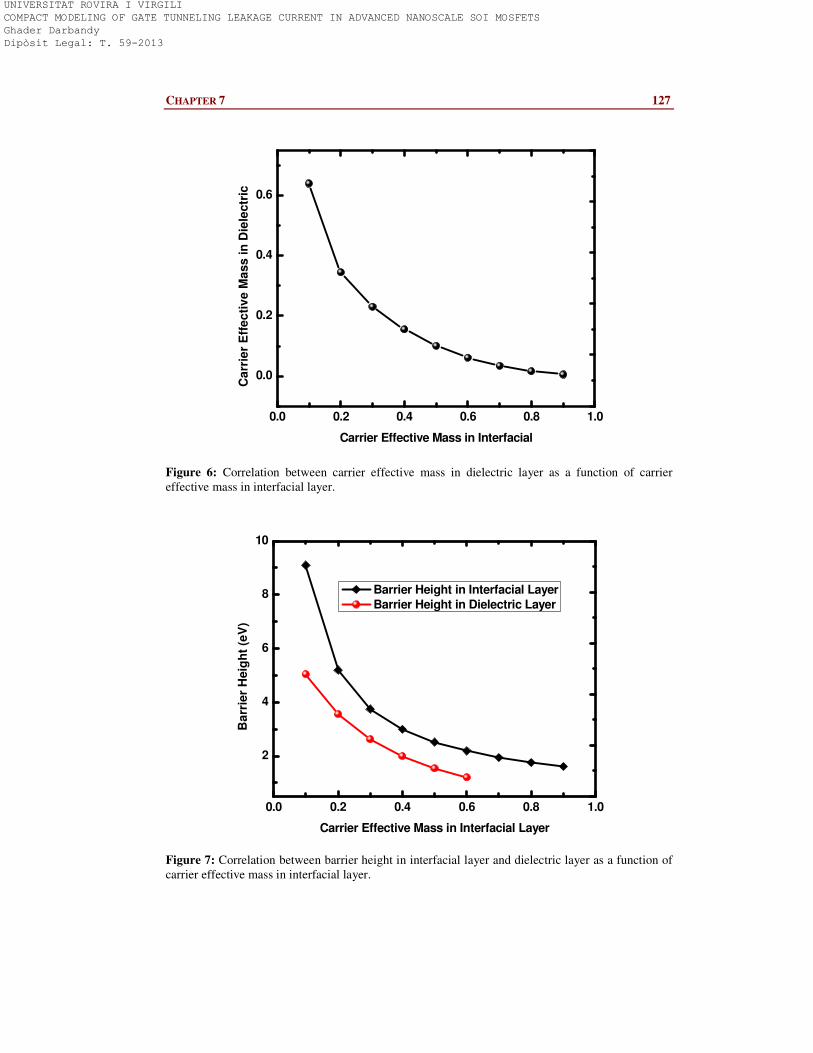
CHAPTER 7 127
0.0 0.2 0.4 0.6 0.8 1.0
0.0
0.2
0.4
0.6
Ca
rrie
r E
ffe
cti
ve
Ma
ss
in
Die
lectr
ic
Carrier Effective Mass in Interfacial
Figure 6: Correlation between carrier effective mass in dielectric layer as a function of carrier
effective mass in interfacial layer.
0.0 0.2 0.4 0.6 0.8 1.0
2
4
6
8
10
Ba
rrie
r H
eig
ht
(eV
)
Carrier Effective Mass in Interfacial Layer
Barrier Height in Interfacial Layer
Barrier Height in Dielectric Layer
Figure 7: Correlation between barrier height in interfacial layer and dielectric layer as a function of
carrier effective mass in interfacial layer.
UNIVERSITAT ROVIRA I VIRGILI COMPACT MODELING OF GATE TUNNELING LEAKAGE CURRENT IN ADVANCED NANOSCALE SOI MOSFETS Ghader Darbandy Dipòsit Legal: T. 59-2013
128 GHADER DARBANDY
5) Conclusion
We have developed automatic parameter extraction techniques in the commercial
package (IC-CAP) to obtain gate leakage current parameter values for Trigate
MOSFET. The extraction approaches have been applied for various conditions and
device geometry and have been found suitable techniques for MOSFET parameter
extraction process. The correlation between gate leakage currents, barrier heights and
carrier effective messes are analyzed in details based on our DT current and TAT
current models, automatic parameter extraction techniques and measured gate leakage
current in Trigate MOSFET. The verification of the extraction techniques and gate
leakage current parameters correlations are discussed and the results show additional
insight into the gate leakage current model and good agreement with the measured data
in Trigate MOSFET.
References
[1] N. G. Tarr, D. L. Pulfrey, and D. S. Camporese, “An Analytic Model for the MIS
Tunnel Junction,” IEEE Trans. Electron Devices, vol. ED-30, No. 12, pp. 1760–1770,
1983
[2] F. Rana, S. Tiwari, and D. A. Buchanan, “Self-consistent modeling of accumulation
layers and tunneling currents through very thin oxides,” Appl. Phys. Lett., vol. 69, no. 8,
p. 1104, 1996.
[3] W-C. Lee, C. Hu. “Modeling CMOS tunneling currents through ultrathin gate oxide
due to conduction and valence-band electron and hole tunneling” IEEE Trans Electron
Dev 2001; 48(7):1366-73.
[4] Chung-Hsun Lin, “Compact Modeling of Nanoscale CMOS”, Ph.D Dissetration,
University of California, Berkeley, 2007
[5] Kanghoon Jeon, “Band-to-Band Tunnel Transistor Design and Modeling for Low
Power Applications”, Ph.D Dissetration, University of California, Berkeley, 2012
UNIVERSITAT ROVIRA I VIRGILI COMPACT MODELING OF GATE TUNNELING LEAKAGE CURRENT IN ADVANCED NANOSCALE SOI MOSFETS Ghader Darbandy Dipòsit Legal: T. 59-2013
CHAPTER 7 129
[6] N. Chevillon, M. Tang, F. Pregaldiny, C. Lallement and M. Madec, "FinFET
Compact Modelling and parameter extraction", Proc. 16th Int. Conf. Mixed Design of
Integrated Circuits and Systems (MIXDES'09)
[7] Joaquın Alvarado1, Benjamin Iniguez, Magali Estrada, Denis Flandre and Antonio
Cerdeira, “Implementation of the symmetric doped double-gate MOSFET model in
Verilog-A for circuit simulation”, Int. J. Numer. Model, 2010; 23:88–106.
[8] Ghader Darbandy, Thomas Gneiting, Heidrun Alius, Joaquin Alvarado, Antonio
Cerdeira and Benjamin Iñiguez, “Automatic Parameter Extraction Techniques with IC-
CAP for Compact Double Gate MOSFET Model”, Semicond. Sci. Technol. To be
submitted
[9] Integrated Circuit Characterization and Analysis Program (IC-CAP) modeling
software, available from http://www.home.agilent.com
[10] Verilog-AMS Language Reference Manual, version 2.3.1, Accellera, 2009.
[11] Ghader Darbandy, Jasmin Aghasi, Josef Seldmeir, Udit Monga, Ivan Garduño,
Antonio Cerdeira, and Benjamin Iñiguez, “Temperature Dependent Compact
Modeling for Gate Tunneling Leakage Current in Double Gate MOSFETs” Solid-State
Electronics, Accepted.
[12] A. Cerdeira, O. Moldovan, B. Iñiguez and M. Estrada, “Modeling of potentials
and threshold voltage for symmetric doped double-gate MOSFETs”, Solid-State
Electronics, vol. 52, no. 5, pp. 830-837, 2008
[13] A. Cerdeira, B. Iñiguez and M. Estrada, “Compact model for short channel
symmetric doped double-gate MOSFET,”, Solid-State Electronics, vol. 52, no. 7, pp.
1064-1070, July 2008.
[14] S. I. Garduño, A. Cerdeira, M. Estrada, J. Alvarado, V. Kilchytska and D. Flandre,
“Contribution of carrier tunneling and gate induced drain leakage effects to the gate
and drain currents of fin–shaped field–effect transistors”, Journal of Applied Physics, 109,
084524 (2011).
UNIVERSITAT ROVIRA I VIRGILI COMPACT MODELING OF GATE TUNNELING LEAKAGE CURRENT IN ADVANCED NANOSCALE SOI MOSFETS Ghader Darbandy Dipòsit Legal: T. 59-2013

130 GHADER DARBANDY
UNIVERSITAT ROVIRA I VIRGILI COMPACT MODELING OF GATE TUNNELING LEAKAGE CURRENT IN ADVANCED NANOSCALE SOI MOSFETS Ghader Darbandy Dipòsit Legal: T. 59-2013
131
General Conclusion
1) We have developed simple and improved analytical models for the direct tunneling
gate leakage current based on a proper WKB tunneling probability approximation. A
theoretical study with only one layer of gate oxide materials has been considered. We
have shown guidelines for finding the appropriate high-k dielectric materials for the 22
nm technological node requirements according to the latest ITRS in DG MOSFETs.
2) We have developed simple and improved gate leakage current models for the two
layer gate oxide materials in DG MOSFETs. We have shown the most promising high-
k candidates for different values of EOT and SiO2 interfacial layer thickness, satisfying
the gate leakage requirements according to the ITRS. They demonstrate that the
materials like HfO2, La2O3, LaAlO3 and Pr2O3 in the hexagonal phase would fulfill the
considered requirements.
3) Analytical models of the direct tunneling gate leakage current are used to determine
the high-k dielectric suitable for the nanoscale UTB SOI MOSFETs structure in cases
with no interfacial layer and with SiO2 as an interfacial layer for the 17nm, 15nm and
14nm technological node requirements. In the ideal case without an interfacial layer,
HfO2 and Lu2O3 were found to be the best gate oxide materials for the 17nm, 15nm
and 14nm technological node requirements.
4) A compact gate leakage current partitioning model has been presented for nanoscale
Double Gate MOSFETs, using analytical models of the direct tunneling gate leakage
current. The influence and impact of the thickness of the interfacial SiO2 layer on the
gate-drain and gate-source components has been shown. The results of the gate
current partitioning components into the drain and source show good agreement with
2D TCAD numerical device simulation.
5) The temperature dependent analytical models of the direct tunneling current in
inversion region and the trap assisted tunneling current in subthreshold regime have
UNIVERSITAT ROVIRA I VIRGILI COMPACT MODELING OF GATE TUNNELING LEAKAGE CURRENT IN ADVANCED NANOSCALE SOI MOSFETS Ghader Darbandy Dipòsit Legal: T. 59-2013
132 GHADER DARBANDY
been developed for DG FinFET with a two dielectric layers gate stack such as
SiON/SiO2. Our analysis based on the gate leakage current measurements in the above
threshold regime for different temperatures shows that the direct tunneling current is
clearly dominant over the trap assisted tunneling, while the opposite happens below
threshold.
6) We have developed automatic parameter extraction techniques for our explicit
compact model in DG MOSFET based on surface potential including short channel
effects (channel length modulation, DIBL, carrier velocity saturation, threshold voltage
roll-off and series resistance). The second derivative of the drain current with respect
to the source-gate potential is verified which is continuous due to a careful
mathematical derivation of our model. The P1 and P2 parameters dependency on the
channel length are investigated and shown for Trigate MOSFETs based on measured
data and extracted parameters.
7) Direct Tunneling and Trap Assisted Tunneling gate leakage current parameters have
been extracted and verified considering automatic parameter extraction approaches for
Trigate MOSFET. The correlation between gate leakage currents, barrier heights and
carrier effective messes are analyzed in details based on our DT current and TAT
current models, automatic parameter extraction techniques and measured gate leakage
current in Trigate MOSFET.
UNIVERSITAT ROVIRA I VIRGILI COMPACT MODELING OF GATE TUNNELING LEAKAGE CURRENT IN ADVANCED NANOSCALE SOI MOSFETS Ghader Darbandy Dipòsit Legal: T. 59-2013

UNIVERSITAT ROVIRA I VIRGILI COMPACT MODELING OF GATE TUNNELING LEAKAGE CURRENT IN ADVANCED NANOSCALE SOI MOSFETS Ghader Darbandy Dipòsit Legal: T. 59-2013


