Embed Size (px)
Citation preview
Yuryev et al. Nanoscale Research Letters 2012, 7:414http://www.nanoscalereslett.com/content/7/1/414
NANO EXPRESS Open Access
Ge/Si(001) heterostructures with dense arraysof Ge quantum dots: morphology, defects,photo-emf spectra and terahertz conductivityVladimir A Yuryev1,2*, Larisa V Arapkina1, Mikhail S Storozhevykh1, Valery A Chapnin1, Kirill V Chizh1,Oleg V Uvarov1, Victor P Kalinushkin1,2, Elena S Zhukova1,3, Anatoly S Prokhorov1,3,Igor E Spektor1 and Boris P Gorshunov1,3
Abstract
Issues of Ge hut cluster array formation and growth at low temperatures on the Ge/Si(001) wetting layer are discussedon the basis of explorations performed by high resolution STM and in-situ RHEED. Dynamics of the RHEED patterns inthe process of Ge hut array formation is investigated at low and high temperatures of Ge deposition. Differentdynamics of RHEED patterns during the deposition of Ge atoms in different growth modes is observed, which reflectsthe difference in adatom mobility and their ‘condensation’ fluxes from Ge 2D gas on the surface for different modes,which in turn control the nucleation rates and densities of Ge clusters. Data of HRTEM studies of multilayer Ge/Siheterostructures are presented with the focus on low-temperature formation of perfect films.Heteroepitaxial Si p–i–n-diodes with multilayer stacks of Ge/Si(001) quantum dot dense arrays built in intrinsicdomains have been investigated and found to exhibit the photo-emf in a wide spectral range from 0.8 to 5μm. Aneffect of wide-band irradiation by infrared light on the photo-emf spectra has been observed. Photo-emf in differentspectral ranges has been found to be differently affected by the wide-band irradiation. A significant increase inphoto-emf is observed in the fundamental absorption range under the wide-band irradiation. The observedphenomena are explained in terms of positive and neutral charge states of the quantum dot layers and the Coulombpotential of the quantum dot ensemble. A new design of quantum dot infrared photodetectors is proposed.By using a coherent source spectrometer, first measurements of terahertz dynamical conductivity (absorptivity)spectra of Ge/Si(001) heterostructures were performed at frequencies ranged from 0.3 to 1.2 THz in the temperatureinterval from 300 to 5 K. The effective dynamical conductivity of the heterostructures with Ge quantum dots has beendiscovered to be significantly higher than that of the structure with the same amount of bulk germanium (notorganized in an array of quantum dots). The excess conductivity is not observed in the structures with the Gecoverage less than 8 A. When a Ge/Si(001) sample is cooled down the conductivity of the heterostructure decreases.
IntroductionArtificial low-dimensional nano-sized objects, like quan-tum dots, quantum wires and quantum wells, as wellas structures based on them, are promising systemsfor improvement of existing devices and for develop-ment of principally new devices for opto-, micro- andnano-electronics. Besides, the investigation of physical
*Correspondence: [email protected] M Prokhorov General Physics Institute of RAS, 38 Vavilov Street, Moscow,119991, Russia2Technopark of GPI RAS, 38 Vavilov Street, Moscow, 119991, RussiaFull list of author information is available at the end of the article
properties of such structures is also of fundamentalimportance. In both regards, amazing perspectives areprovided when playing around with quantum dots thatcan be considered as artificial atoms with a controllednumber of charge carriers that have a discrete energyspectrum [1,2]. Arrays of a large number of quantum dotsincluding multilayer heterostructures make it possible tocreate artificial “solids” whose properties can be control-lably changed by varying the characteristics of constituentelements (“atoms”) and/or the environment (semiconduc-tor matrix). The rich set of exciting physical properties
© 2012 Yuryev et al.; licensee Springer. This is an Open Access article distributed under the terms of the Creative CommonsAttribution License (http://creativecommons.org/licenses/by/2.0), which permits unrestricted use, distribution, and reproductionin any medium, provided the original work is properly cited.
Yuryev et al. Nanoscale Research Letters 2012, 7:414 Page 2 of 18http://www.nanoscalereslett.com/content/7/1/414
in this kind of systems originates from single-particleand collective interactions that depend on the numberand mobility of carriers in quantum dots, Coulomb inter-action between the carriers inside a quantum dot andin neighbouring quantum dots, charge coupling betweenneighbouring quantum dots, polaron and exciton effects,etc. Since characteristic energy scales of these interactions(distance between energy levels, Coulomb interactionbetween charges in quantum dots, one- and multiparticleexciton and polaron effects, plasmon excitations, etc.) areof order of several meV [3-5], an appropriate experimen-tal tool for their study is provided by optical spectroscopyin the far-infrared and terahertz bands.To get access to the effects, one has to extend the oper-
ation range of the spectrometers to the correspondingfrequency domain that is to the terahertz frequency band.Because of inaccessibility of this band, and especially of itslowest frequency part, below 1 THz (that is � 33 cm−1),for standard infrared Fourier-transform spectrometers,correspondent data is presently missing in the literature.In this paper, we present the results of the first detailedmeasurements of the absolute dynamical (AC) conductiv-ity of multilayer Ge/Si heterostructures with Ge quantumdots, at terahertz and sub-terahertz frequencies and in thetemperature range from 5 to 300K.In addition, for at least two tens of years, multilayer
Ge/Si heterostructures with quantum dots have been can-didates to the role of photosensitive elements of mono-lithic IR arrays promising to replace and excel platinumsilicide in this important brunch of the sensor technol-ogy [6-8]. Unfortunately, to date achievements in this fieldhave been less than modest.We believe that this state of affairs may be improved
by rigorous investigation of formation, defects and otheraspects of materials science of such structures, especiallythose which may affect device performance and reliabil-ity, focusing on identification of reasons of low quantumefficiency and detectivity, high dark current and tend todegrade with time as well as on search of ways to over-come these deficiences. New approaches to device archi-tecture and design as well as to principles of functioningare also desirable.This article reports our latest data on morphology and
defects of Ge/Si heterostructures. On the basis of ourrecent results on the photo-emf in the Si p–i–n-structureswith Ge quantum dots, which are also reported in thisarticle, we propose a new design of photovoltaic quantumdot infrared photodetectors.
MethodsEquipment and techniquesThe Ge/Si samples were grown and characterized usingan integrated ultrahigh vacuum instrument [9-12] builton the basis of the Riber SSC 2 surface science center
with the EVA32 molecular-beam epitaxy (MBE) chamberequipped with the RH20 reflection high-energy electrondiffraction (RHEED) tool (Staib Instruments) and con-nected through a transfer line to the GPI-300 ultrahighvacuum scanning tunnelling microscope (STM) [13-15].Sources with the electron beam evaporation were used forGe or Si deposition. A Knudsen effusion cells was utilizedif boron doping was applied for QDIP p–i–n-structureformation. The pressure of about 5×10⁻⁹ Torr was kept inthe preliminary sample cleaning (annealing) chamber. TheMBE chamber was evacuated down to about 10−11 Torrbefore processes; the pressure increased to nearly 2 ×10⁻⁹ Torr at most during the Si substrate cleaning and10−9 Torr during Ge or Si deposition. The residual gaspressure did not exceed 10−10 Torr in the STM chamber.Additional details of the experimental instruments andprocess control can be found in Ref. [12].RHEED measurements were carried out in situ, i.e.,
directly in the MBE chamber during a process [10]. STMimages were obtained in the constant tunnelling currentmode at the room temperature. The STM tip was zero-biased while the sample was positively or negatively biasedwhen scanned in empty- or filled-states imaging mode.Structural properties of the Ge/Si films were explored byusing the Carl Zeiss Libra-200 FE HR HRTEM.The images were processed using the WSxM software
[16].For obtaining spectra of photo-electromotive force
(photo-emf) a setup enabling sample illumination by twoindependent beams was used; one of the beams was awide-band infrared (IR) radiation, generated by a tungstenbulb, passed through a filter of Si or Ge (bias lighting) andthe other was a beam-chopper modulated narrow-bandradiation cut from globar emission by an IR monochro-mator tunable in the range from 0.8 to 20μm. The spectrawere taken at the chopping frequency of 12.5 Hz at tem-peratures ranged from 300 to 70 K and a widely variedpower of the bias lighting.The measurements of the terahertz dynamic conduc-
tivity and absorptivity of Ge/Si heterostructures at roomand cryogenic temperatures (down to 5 K) have been per-formed using the spectrometer based on backward-waveoscillators (BWO) as radiation sources. This advancedexperimental technique will be described in detail belowin a separate section.
Sample preparation proceduresPreparation of samples for STM and RHEEDInitial samples for STM and RHEED studies were 8 ×8 mm2 squares cut from the specially treated com-mercial boron-doped Czochralski-grown (CZ) Si(100)wafers (p-type, ρ = 12 � cm). After washing and chemi-cal treatment following the standard procedure describedelsewhere [17], which included washing in ethanol,
Yuryev et al. Nanoscale Research Letters 2012, 7:414 Page 3 of 18http://www.nanoscalereslett.com/content/7/1/414
etching in the mixture of HNO3 and HF and rinsingin the deionized water [12], the silicon substrates wereloaded into the airlock and transferred into the prelim-inary annealing chamber where they were outgassed atthe temperature of around 565°C for more than 6 h. Afterthat, the substrates were moved for final treatment andGe deposition into the MBE chamber where they weresubjected to two-stages annealing during heating withstoppages at 600°C for 5min and at 800°C for 3min [9,10].The final annealing at the temperature greater than 900°Cwas carried out for nearly 2.5min with themaximum tem-perature of about 925°C (1.5min). Then, the temperaturewas rapidly lowered to about 750°C. The rate of the fur-ther cooling was around 0.4°C/s that corresponded to the‘quenching’ mode applied in [10]. The surfaces of the sil-icon substrates were completely purified of the oxide filmas a result of this treatment [10,18,19].Ge was deposited directly on the deoxidized Si(001) sur-
face. The deposition rate was varied from about 0.1 to0.15 A/s; the effective Ge film thickness (hGe) was variedfrom 3 to 18 A for different samples. The substrate tem-perature during Ge deposition (Tgr) was 360°C for thelow-temperature mode and 600 or 650°C for the high-temperature mode. The rate of the sample cooling downto the room temperature was approximately 0.4°C/s afterthe deposition.
Preparation ofmultilayer structuresGe/Si heterostructures with buried Ge layers were grownon CZ p-Si(100):B wafers (ρ = 12 � cm) washed andoutgassed as described above. Deoxidized Si(001) surfaceswere prepared by a process allowed us to obtain clean sub-strate surfaces (this was verified by STM and RHEED) andperfect epitaxial interfaces with Si buffer layers (verifiedby HRTEM): the wafers were annealed at 800°C under Siflux of � 0.1 A/s until a total amount of the deposited Si,expressed in the units of the Si film thickness indicated bythe film thickness monitor, reached 30 A; 2-minute stop-pages of Si deposition weremade first twice after every 5 Aand then twice after every 10 A.Afterwards, a ∼ 100 nm thick Si buffer was deposited
on the prepared surface at the temperature of ∼ 650°C.Then, a single Ge layer or a multilayer Ge/Si structurewas grown. A number of Ge layers in multilayer structuresreached 15 but usually was 5; their effective thickness(hGe), permanent for each sample, was varied from sam-ple to sample in the range from 4 to 18 A; the thickness ofthe Si spacers (hSi) was ∼ 50 nm. The Ge deposition tem-perature was ∼ 360°C, Si spacers were grown at ∼ 530°C.A heterostructure formed in such a way was capped bya ∼ 100 nm thick Si layer grown at ∼ 530°C. All layerswere undoped.The samples were quenched after the growth at the rate
of ∼ 0.4°C/s.
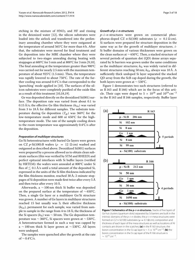
Growth of p–i–n-structuresp–i–n-structures were grown on commercial phos-phorus-doped CZ n-Si(100) substrates (ρ = 0.1� cm).Si surfaces were prepared for structure deposition in thesame way as for the growth of multilayer structures. i-Si buffer domains of various thicknesses were grown onthe clean surfaces at ∼ 650°C. Then, a stacked structure ofseveral periods of quantum dot (QD) dense arrays sepa-rated by Si barriers was grown under the same conditionsas the multilayer structures; hSi was widely varied in dif-ferent structures reaching 50 nm; hGe always was 10 A. Asufficiently thick undoped Si layer separated the stackedQD array from the Si:B cap doped during the growth, theboth layers were grown at ∼ 530°C.Figure 1 demonstrates two such structures (referred to
as R 163 and R 166) which are in the focus of this arti-cle. Their caps were doped to 5 × 10¹⁸ and 1019 cm−3
in the R 163 and R 166 samples, respectively. Buffer layer
(a)
(b)
Figure 1 Schematics of the p–i–n-structures. Stacks of five layers ofGe hut clusters (quantum dots) separated by Si barriers are built in theintrinsic domains of the p–i–n diodes; the p–i–nmesa structures wereformed on CZ n-Si(100) substrates (ρ = 0.1� cm); composition andthickness of each layer of the mesa structures as well as locations of Alcontacts are shown in the scatches; (a) in the R 163 structure, theboron concentration in the Si cap layer is ∼ 5 × 1018 cm−3; (b) theboron concentration in the Si cap layer of the R 166 structure is∼ 1019 cm−3.
Yuryev et al. Nanoscale Research Letters 2012, 7:414 Page 4 of 18http://www.nanoscalereslett.com/content/7/1/414
and barrier thicknesses were 99 and 8 nm in the R 163structure and 1690 and 30 nm in R 166.Mesas were formed on samples for photoelectric mea-
surements. Ohmic contacts were formed by thermaldeposition of aluminum.
Terahertz BWO-spectroscopyThe BWO-spectrometers provide broad-band operation(frequencies ν ranging from 30 GHz to 2 THz), highfrequency resolution (�ν/ν = 10−5), broad dynamicrange (40–50 dB), continuous frequency tuning and, veryimportantly, the possibility of direct determination ofspectra of any “optical” parameter, like complex conduc-tivity, complex dielectric permittivity, etc. (‘direct’ meansthat no Kramers–Kronig analysis—typical for far-infraredFourier transform spectroscopy—is needed). The prin-ciple of operation of BWO-spectrometers is describedin details in the literature (see, e.g., [20,21]). It is basedon measurement of the complex transmission coefficientTr∗ = Tr exp(iϕ) of a plane-parallel sample with subse-quent calculation of the spectra of its optical parametersfrom those of the transmission coefficient amplitudeTr(ν)
and the phase ϕ(ν). The corresponding expression can bewritten as [22,23]
Tr∗ = Tr exp(iϕ) = T12T21 exp(iδ)1 + T12T21 exp(2iδ)
. (1)
Here
Tpq = tpq exp(iϕpq), t2pq =4
(n2p + k2p
)(kp + kq)2 + (np + nq)2
,
ϕpq = arctan{
kpnp − kqnqn2p + k2p + npnq + kpkq
}
are Fresnel coefficients for the interfaces ‘air–sample’,indices p, q = 1, 2 correspond: ‘1’ to air (refractive indexn1 = 1, extinction coefficient k1 = 0) and ‘2’ to the mate-rial of the sample (n2, k2), δ = 2πd
λ(n2 + ik2), d is the
sample thickness, λ is the radiation wavelength. The sam-ple parameters (for instance, n2 and k2 ) are found for eachfixed frequency by solving two coupled equations for thetwo unknowns, Tr(n2, k2, ν) = Trexp(ν) and ϕ(n2, k2, ν) =ϕexp(ν) [here Trexp(ν) and ϕexp(ν) are the measured quan-tities]. The so-found values of n2(ν) and k2(ν) can thenbe used to derive the spectra of the complex permittiv-ity ε∗(ν) = ε′(ν) + iε′′(ν) = n22 − k22 + 2in2k2, complexconductivity σ ∗(ν) = σ1(ν) + iσ2(ν) = νn2k2 + iν(ε∞ −ε′)/2, etc. (ε∞ is the high-frequency contribution to thepermittivity).If the sample is characterized by low enough absorption
coefficient, Fabry–Perot-like interference of the radiation
within the plane-parallel layer leads to an interferencemaxima and minima in the transmission coefficientspectra. In this case there is no need to measure the phaseshift spectra since the pairs of optical quantities of thesample can be calculated from the transmission coefficientspectrum alone: the absorptive part (like ε′′ or σ1) is deter-mined from the interferometric maxima amplitudes andthe refractive part (like ε′ or n) is calculated from theirpositions [20,21].When measuring the dielectric response of the films
(like heterostructures in the present case) on dielectricsubstrates, first the dielectric properties of the substratematerial are determined by standard techniques justdescribed. Next, one measures the spectra of the trans-mission coefficient and of the phase shift of the film-substrate system, and it is these spectra that are used toderive the dielectric response of the film by solving twocoupled equations for two unknowns—“optical” param-eters of the film. The corresponding expression for thecomplex transmission coefficient of a two-layer systemcan be written as [22,23]:
Tr∗1234 = Tr exp(iϕ)
= T12T23T34 exp{i(δ2 + δ3)}1+T23T34 exp(2iδ3)+T12T23 exp(2iδ2)+T12T34 exp{2i(δ2+δ3)} ,
(2)
where indices 1 and 4 refer to the media on the twosides of the sample, i.e., of the film on substrate, δp =(np + ikp), with dp being the film and substrate thick-nesses (p = 2, 3). The other notations are the same as inEq. (1). The measurements are performed in a quasiop-tical configuration, no waveguides are used [20,21] andthis makes measurement schemes extremely flexible. Allmeasurement and analysis procedures are PC-controlled.Most important parameters of the BWO-spectrometerare summarized in Table 1.
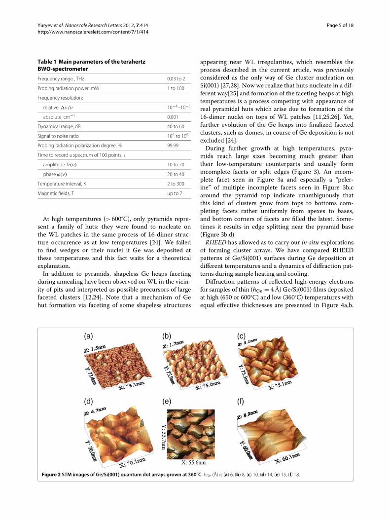
Results and discussionMorphology and defectsSTM and RHEED study of Ge/Si(001) QD arrays: morphologyand formationPreviously, we have shown in a number of STM studies[9,11,12,24-26] that the process of the hut array nucleationand growth at low temperatures starts from occurrence oftwo types of 16-dimer nuclei [25] on wetting layer (WL)patches of 4-ML height [26] giving rise to two knownspecies of {105}-faceted clusters—pyramids and wedges[9]—which then, growing in height (both types) andin length (wedges), gradually occupy the whole wettinglayer, coalless and start to form a nanocrystalline Ge film(Figure 2) [11,12]. This is a life cycle of hut arrays at thetemperatures < 600°C. We refer to cluster growth at thesetemperatures as the low-temperature mode.
Yuryev et al. Nanoscale Research Letters 2012, 7:414 Page 5 of 18http://www.nanoscalereslett.com/content/7/1/414
Table 1 Main parameters of the terahertzBWO-spectrometer
Frequency range , THz 0.03 to 2
Probing radiation power, mW 1 to 100
Frequency resolution:
relative, �ν/ν 10−4–10−5
absolute, cm−1 0.001
Dynamical range, dB 40 to 60
Signal to noise ratio 104 to 106
Probing radiation polarization degree, % 99.99
Time to record a spectrum of 100 points, s:
amplitude Tr(ν) 10 to 20
phase ϕ(ν) 20 to 40
Temperature interval, K 2 to 300
Magnetic fields, T up to 7
At high temperatures (> 600°C), only pyramids repre-sent a family of huts: they were found to nucleate onthe WL patches in the same process of 16-dimer struc-ture occurrence as at low temperatures [24]. We failedto find wedges or their nuclei if Ge was deposited atthese temperatures and this fact waits for a theoreticalexplanation.In addition to pyramids, shapeless Ge heaps faceting
during annealing have been observed on WL in the vicin-ity of pits and interpreted as possible precursors of largefaceted clusters [12,24]. Note that a mechanism of Gehut formation via faceting of some shapeless structures
appearing near WL irregularities, which resembles theprocess described in the current article, was previouslyconsidered as the only way of Ge cluster nucleation onSi(001) [27,28]. Now we realize that huts nucleate in a dif-ferent way[25] and formation of the faceting heaps at hightemperatures is a process competing with appearance ofreal pyramidal huts which arise due to formation of the16-dimer nuclei on tops of WL patches [11,25,26]. Yet,further evolution of the Ge heaps into finalized facetedclusters, such as domes, in course of Ge deposition is notexcluded [24].During further growth at high temperatures, pyra-
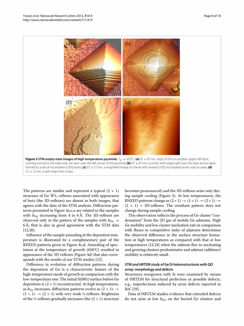
mids reach large sizes becoming much greater thantheir low-temperature counterparts and usually formincomplete facets or split edges (Figure 3). An incom-plete facet seen in Figure 3a and especially a “peler-ine” of multiple incomplete facets seen in Figure 3b,caround the pyramid top indicate unambiguously thatthis kind of clusters grow from tops to bottoms com-pleting facets rather uniformly from apexes to bases,and bottom corners of facets are filled the latest. Some-times it results in edge splitting near the pyramid base(Figure 3b,d).RHEED has allowed as to carry our in-situ explorations
of forming cluster arrays. We have compared RHEEDpatterns of Ge/Si(001) surfaces during Ge deposition atdifferent temperatures and a dynamics of diffraction pat-terns during sample heating and cooling.Diffraction patterns of reflected high-energy electrons
for samples of thin (hGe = 4 A) Ge/Si(001) films depositedat high (650 or 600°C) and low (360°C) temperatures withequal effective thicknesses are presented in Figure 4a,b.
(a) (b) (c)
(d) (e) (f)
Figure 2 STM images of Ge/Si(001) quantum dot arrays grown at 360°C. hGe (A) is (a) 6, (b) 8, (c) 10, (d) 14, (e) 15, (f) 18.
Yuryev et al. Nanoscale Research Letters 2012, 7:414 Page 6 of 18http://www.nanoscalereslett.com/content/7/1/414
(a) (b)
(c) (d)
Figure 3 STM empty-state images of high-temperature pyramids. Tgr = 650°C; (a) 87 × 87 nm, steps of the incomplete upper left facet,running normal to the base side, are seen near the left corner of the pyramid; (b) 87 × 87 nm, a cluster with edges split near the base and an apexformed by a set of incomplete {105} facets; (c) 57 × 57 nm, a magnified image of a facet with several {105} incomplete facets near an apex; (d)22 × 22 nm, a split edge near a base.
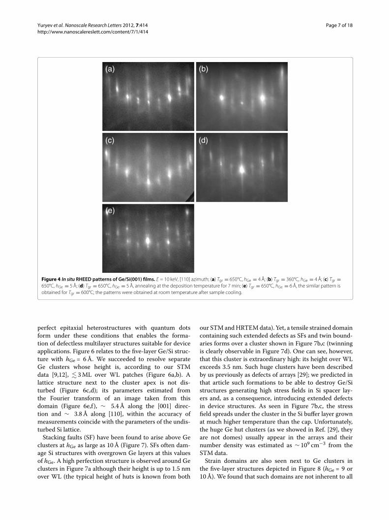
The patterns are similar and represent a typical (2 × 1)structure of Ge WL; reflexes associated with appearanceof huts (the 3D-reflexes) are absent in both images, thatagrees with the data of the STM analysis. Diffraction pat-terns presented in Figure 4a,c,e are related to the sampleswith hGe increasing from 4 to 6 A. The 3D-reflexes areobserved only in the pattern of the samples with hGe =6 A, that is also in good agreement with the STM data[12,26].Influence of the sample annealing at the deposition tem-
perature is illustrated by a complimentary pair of theRHEED patterns given in Figure 4c,d. Annealing of spec-imens at the temperature of growth (650°C) resulted inappearance of the 3D-reflexes (Figure 4d) that also corre-sponds with the results of our STM studies [12].Difference in evolution of diffraction patterns during
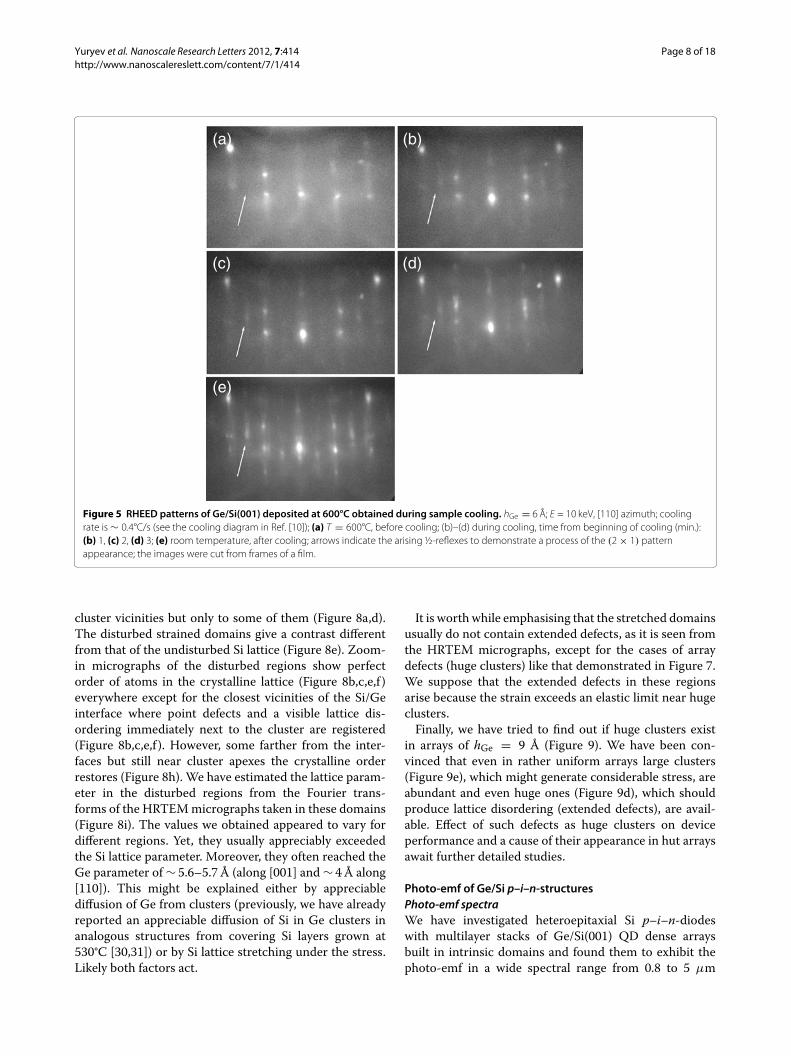
the deposition of Ge is a characteristic feature of thehigh-temperature mode of growth in comparison with thelow-temperature one. The initial Si(001) surface before Gedeposition is (2× 1) reconstructed. At high temperatures,as hGe increases, diffraction patterns evolve as (2 × 1) →(1 × 1) → (2 × 1) with very weak ½-reflexes. Brightnessof the ½-reflexes gradually increases (the (2× 1) structure
becomes pronounced) and the 3D-reflexes arise only dur-ing sample cooling (Figure 5). At low temperatures, theRHEED patterns change as (2×1) → (1×1) → (2×1) →(2 × 1) + 3D-reflexes. The resultant pattern does notchange during sample cooling.This observation reflects the process of Ge cluster “con-
densation” from the 2D gas of mobile Ge adatoms. HighGemobility and low cluster nucleation rate in comparisonwith fluxes to competitive sinks of adatoms determinesthe observed difference in the surface structure forma-tion at high temperatures as compared with that at lowtemperatures [12,24] when the adatom flux to nucleatingand growing clusters predominates and adatom (addimer)mobility is relatively small.
STM and HRTEM study of Ge/Si heterostructures with QDarray: morphology and defectsStructures overgrown with Si were examined by meansof HRTEM for structural perfection or possible defects,e.g., imperfections induced by array defects reported inRef. [29].Data of HRTEM studies evidence that extended defects
do not arise at low hGe on the buried Ge clusters and
Yuryev et al. Nanoscale Research Letters 2012, 7:414 Page 7 of 18http://www.nanoscalereslett.com/content/7/1/414
(a) (b)
(c) (d)
(e)
Figure 4 In situ RHEED patterns of Ge/Si(001) films. E = 10 keV, [110] azimuth; (a) Tgr = 650°C, hGe = 4 A; (b) Tgr = 360°C, hGe = 4 A; (c) Tgr =650°C, hGe = 5 A; (d) Tgr = 650°C, hGe = 5 A, annealing at the deposition temperature for 7 min; (e) Tgr = 650°C, hGe = 6 A, the similar pattern isobtained for Tgr = 600°C; the patterns were obtained at room temperature after sample cooling.
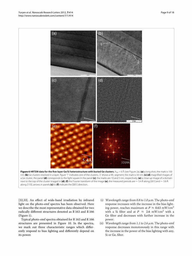
perfect epitaxial heterostructures with quantum dotsform under these conditions that enables the forma-tion of defectless multilayer structures suitable for deviceapplications. Figure 6 relates to the five-layer Ge/Si struc-ture with hGe = 6 A. We succeeded to resolve separateGe clusters whose height is, according to our STMdata [9,12], � 3ML over WL patches (Figure 6a,b). Alattice structure next to the cluster apex is not dis-turbed (Figure 6c,d); its parameters estimated fromthe Fourier transform of an image taken from thisdomain (Figure 6e,f ), ∼ 5.4 A along the [001] direc-tion and ∼ 3.8 A along [110], within the accuracy ofmeasurements coincide with the parameters of the undis-turbed Si lattice.Stacking faults (SF) have been found to arise above Ge
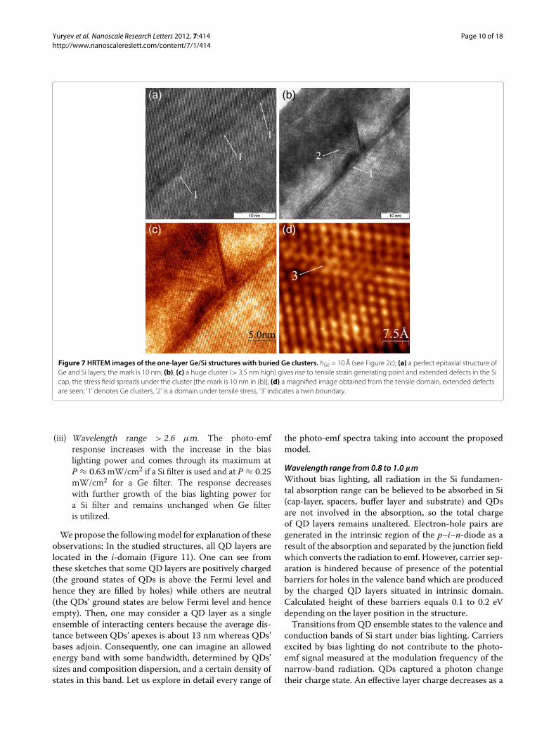
clusters at hGe as large as 10 A (Figure 7). SFs often dam-age Si structures with overgrown Ge layers at this valuesof hGe. A high perfection structure is observed around Geclusters in Figure 7a although their height is up to 1.5 nmover WL (the typical height of huts is known from both
our STM andHRTEMdata). Yet, a tensile strained domaincontaining such extended defects as SFs and twin bound-aries forms over a cluster shown in Figure 7b,c (twinningis clearly observable in Figure 7d). One can see, however,that this cluster is extraordinary high: its height over WLexceeds 3.5 nm. Such huge clusters have been describedby us previously as defects of arrays [29]; we predicted inthat article such formations to be able to destroy Ge/Sistructures generating high stress fields in Si spacer lay-ers and, as a consequence, introducing extended defectsin device structures. As seen in Figure 7b,c, the stressfield spreads under the cluster in the Si buffer layer grownat much higher temperature than the cap. Unfortunately,the huge Ge hut clusters (as we showed in Ref. [29], theyare not domes) usually appear in the arrays and theirnumber density was estimated as ∼ 109 cm−3 from theSTM data.Strain domains are also seen next to Ge clusters in
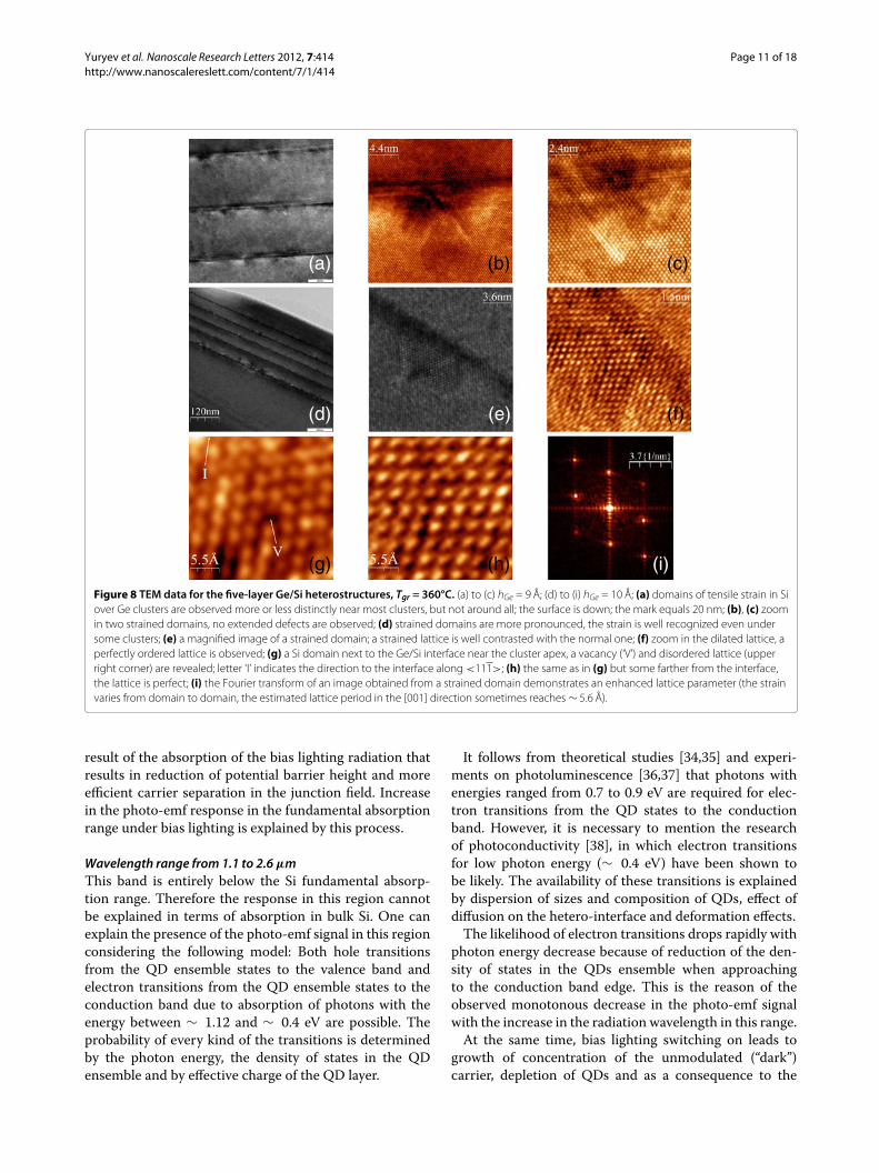
the five-layer structures depicted in Figure 8 (hGe = 9 or10 A). We found that such domains are not inherent to all
Yuryev et al. Nanoscale Research Letters 2012, 7:414 Page 8 of 18http://www.nanoscalereslett.com/content/7/1/414
(a) (b)
(c) (d)
(e)
Figure 5 RHEED patterns of Ge/Si(001) deposited at 600°C obtained during sample cooling. hGe = 6 A; E = 10 keV, [110] azimuth; coolingrate is ∼ 0.4°C/s (see the cooling diagram in Ref. [10]); (a) T = 600°C, before cooling; (b)–(d) during cooling, time from beginning of cooling (min.):(b) 1, (c) 2, (d) 3; (e) room temperature, after cooling; arrows indicate the arising ½-reflexes to demonstrate a process of the (2 × 1) patternappearance; the images were cut from frames of a film.
cluster vicinities but only to some of them (Figure 8a,d).The disturbed strained domains give a contrast differentfrom that of the undisturbed Si lattice (Figure 8e). Zoom-in micrographs of the disturbed regions show perfectorder of atoms in the crystalline lattice (Figure 8b,c,e,f )everywhere except for the closest vicinities of the Si/Geinterface where point defects and a visible lattice dis-ordering immediately next to the cluster are registered(Figure 8b,c,e,f ). However, some farther from the inter-faces but still near cluster apexes the crystalline orderrestores (Figure 8h). We have estimated the lattice param-eter in the disturbed regions from the Fourier trans-forms of the HRTEMmicrographs taken in these domains(Figure 8i). The values we obtained appeared to vary fordifferent regions. Yet, they usually appreciably exceededthe Si lattice parameter. Moreover, they often reached theGe parameter of ∼ 5.6–5.7 A (along [001] and ∼ 4 A along[110]). This might be explained either by appreciablediffusion of Ge from clusters (previously, we have alreadyreported an appreciable diffusion of Si in Ge clusters inanalogous structures from covering Si layers grown at530°C [30,31]) or by Si lattice stretching under the stress.Likely both factors act.
It is worth while emphasising that the stretched domainsusually do not contain extended defects, as it is seen fromthe HRTEM micrographs, except for the cases of arraydefects (huge clusters) like that demonstrated in Figure 7.We suppose that the extended defects in these regionsarise because the strain exceeds an elastic limit near hugeclusters.Finally, we have tried to find out if huge clusters exist
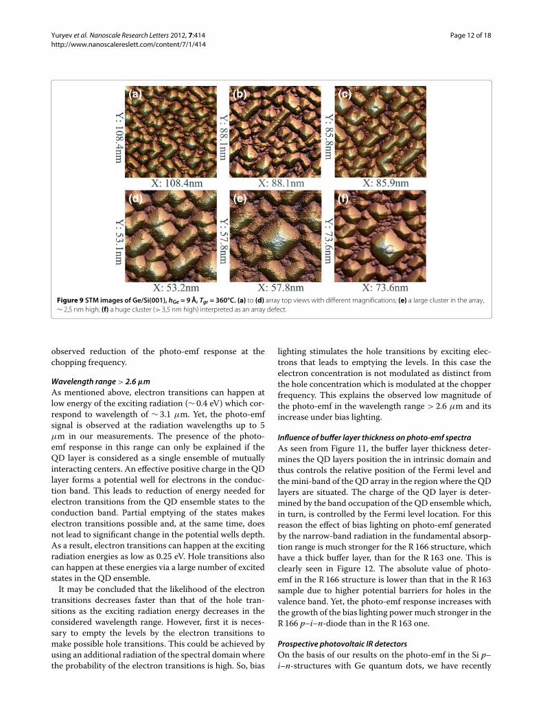
in arrays of hGe = 9 A (Figure 9). We have been con-vinced that even in rather uniform arrays large clusters(Figure 9e), which might generate considerable stress, areabundant and even huge ones (Figure 9d), which shouldproduce lattice disordering (extended defects), are avail-able. Effect of such defects as huge clusters on deviceperformance and a cause of their appearance in hut arraysawait further detailed studies.
Photo-emf of Ge/Si p–i–n-structuresPhoto-emf spectraWe have investigated heteroepitaxial Si p–i–n-diodeswith multilayer stacks of Ge/Si(001) QD dense arraysbuilt in intrinsic domains and found them to exhibit thephoto-emf in a wide spectral range from 0.8 to 5 μm
Yuryev et al. Nanoscale Research Letters 2012, 7:414 Page 9 of 18http://www.nanoscalereslett.com/content/7/1/414
(a) (b)
(c) (d)
(e) (f)
Figure 6 HRTEM data for the five-layer Ge/Si heterostructure with buried Ge clusters. hGe = 6 A (see Figure 2a); (a) a long shot, the mark is 100nm; (b) Ge clusters resolved in a layer, figure ‘1’ indicates one of the clusters, ‘2’ shows a WL segment; the mark is 50 nm; (c),(d)magnified images ofa Ge cluster, the panel (d) corresponds to the light square in the panel (c); the marks are 10 and 5 nm, respectively; (e) a close-up image of a domainnext to the top of the cluster imaged in (d); (f) the Fourier transform of the image (e), the measured periods are ∼ 5.4 A along [001] and ∼ 3.8 Aalong [110]; arrows in panels (c) to (f) indicate the [001] direction.
[32,33]. An effect of wide-band irradiation by infraredlight on the photo-emf spectra has been observed. Herewe describe the most representative data obtained for tworadically different structures denoted as R 163 and R 166(Figure 1).Typical photo-emf spectra obtained for R 163 and R 166
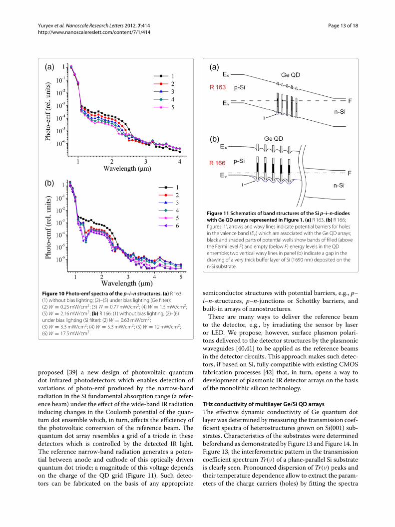
structures are presented in Figure 10. In the spectra,we mark out three characteristic ranges which differ-ently respond to bias lighting and differently depend onits power.
(i) Wavelength range from 0.8 to 1.0μm. The photo-emfresponse increases with the increase in the bias light-ing power, reaches maximum at P ≈ 0.63 mW/cm2
with a Si filter and at P ≈ 2.6 mW/cm2 with aGe filter and decreases with further increase in thepower.
(ii) Wavelength range from 1.1 to 2.6μm. The photo-emfresponse decreases monotonously in this range withthe increase in the power of the bias lighting with any,Si or Ge, filter.
Yuryev et al. Nanoscale Research Letters 2012, 7:414 Page 10 of 18http://www.nanoscalereslett.com/content/7/1/414
(a) (b)
(c) (d)
Figure 7 HRTEM images of the one-layer Ge/Si structures with buried Ge clusters. hGe = 10 A (see Figure 2c); (a) a perfect epitaxial structure ofGe and Si layers; the mark is 10 nm; (b), (c) a huge cluster (> 3,5 nm high) gives rise to tensile strain generating point and extended defects in the Sicap, the stress field spreads under the cluster [the mark is 10 nm in (b)]; (d) a magnified image obtained from the tensile domain, extended defectsare seen; ‘1’ denotes Ge clusters, ‘2’ is a domain under tensile stress, ‘3’ indicates a twin boundary.
(iii) Wavelength range > 2.6 μm. The photo-emfresponse increases with the increase in the biaslighting power and comes through its maximum atP ≈ 0.63mW/cm2 if a Si filter is used and at P ≈ 0.25mW/cm2 for a Ge filter. The response decreaseswith further growth of the bias lighting power fora Si filter and remains unchanged when Ge filteris utilized.
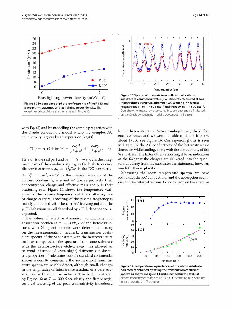
Wepropose the followingmodel for explanation of theseobservations: In the studied structures, all QD layers arelocated in the i-domain (Figure 11). One can see fromthese sketches that some QD layers are positively charged(the ground states of QDs is above the Fermi level andhence they are filled by holes) while others are neutral(the QDs’ ground states are below Fermi level and henceempty). Then, one may consider a QD layer as a singleensemble of interacting centers because the average dis-tance between QDs’ apexes is about 13 nm whereas QDs’bases adjoin. Consequently, one can imagine an allowedenergy band with some bandwidth, determined by QDs’sizes and composition dispersion, and a certain density ofstates in this band. Let us explore in detail every range of
the photo-emf spectra taking into account the proposedmodel.
Wavelength range from 0.8 to 1.0μmWithout bias lighting, all radiation in the Si fundamen-tal absorption range can be believed to be absorbed in Si(cap-layer, spacers, buffer layer and substrate) and QDsare not involved in the absorption, so the total chargeof QD layers remains unaltered. Electron-hole pairs aregenerated in the intrinsic region of the p–i–n-diode as aresult of the absorption and separated by the junction fieldwhich converts the radiation to emf. However, carrier sep-aration is hindered because of presence of the potentialbarriers for holes in the valence band which are producedby the charged QD layers situated in intrinsic domain.Calculated height of these barriers equals 0.1 to 0.2 eVdepending on the layer position in the structure.Transitions from QD ensemble states to the valence and
conduction bands of Si start under bias lighting. Carriersexcited by bias lighting do not contribute to the photo-emf signal measured at the modulation frequency of thenarrow-band radiation. QDs captured a photon changetheir charge state. An effective layer charge decreases as a
Yuryev et al. Nanoscale Research Letters 2012, 7:414 Page 11 of 18http://www.nanoscalereslett.com/content/7/1/414
(a) (b) (c)
(d) (e) (f)
(g) (h) (i)
Figure 8 TEM data for the five-layer Ge/Si heterostructures, Tgr = 360°C. (a) to (c) hGe = 9 A; (d) to (i) hGe = 10 A; (a) domains of tensile strain in Siover Ge clusters are observed more or less distinctly near most clusters, but not around all; the surface is down; the mark equals 20 nm; (b), (c) zoomin two strained domains, no extended defects are observed; (d) strained domains are more pronounced, the strain is well recognized even undersome clusters; (e) a magnified image of a strained domain; a strained lattice is well contrasted with the normal one; (f) zoom in the dilated lattice, aperfectly ordered lattice is observed; (g) a Si domain next to the Ge/Si interface near the cluster apex, a vacancy (‘V’) and disordered lattice (upperright corner) are revealed; letter ‘I’ indicates the direction to the interface along <111>; (h) the same as in (g) but some farther from the interface,the lattice is perfect; (i) the Fourier transform of an image obtained from a strained domain demonstrates an enhanced lattice parameter (the strainvaries from domain to domain, the estimated lattice period in the [001] direction sometimes reaches ∼ 5.6 A).
result of the absorption of the bias lighting radiation thatresults in reduction of potential barrier height and moreefficient carrier separation in the junction field. Increasein the photo-emf response in the fundamental absorptionrange under bias lighting is explained by this process.
Wavelength range from 1.1 to 2.6μmThis band is entirely below the Si fundamental absorp-tion range. Therefore the response in this region cannotbe explained in terms of absorption in bulk Si. One canexplain the presence of the photo-emf signal in this regionconsidering the following model: Both hole transitionsfrom the QD ensemble states to the valence band andelectron transitions from the QD ensemble states to theconduction band due to absorption of photons with theenergy between ∼ 1.12 and ∼ 0.4 eV are possible. Theprobability of every kind of the transitions is determinedby the photon energy, the density of states in the QDensemble and by effective charge of the QD layer.
It follows from theoretical studies [34,35] and experi-ments on photoluminescence [36,37] that photons withenergies ranged from 0.7 to 0.9 eV are required for elec-tron transitions from the QD states to the conductionband. However, it is necessary to mention the researchof photoconductivity [38], in which electron transitionsfor low photon energy (∼ 0.4 eV) have been shown tobe likely. The availability of these transitions is explainedby dispersion of sizes and composition of QDs, effect ofdiffusion on the hetero-interface and deformation effects.The likelihood of electron transitions drops rapidly with
photon energy decrease because of reduction of the den-sity of states in the QDs ensemble when approachingto the conduction band edge. This is the reason of theobserved monotonous decrease in the photo-emf signalwith the increase in the radiation wavelength in this range.At the same time, bias lighting switching on leads to
growth of concentration of the unmodulated (“dark”)carrier, depletion of QDs and as a consequence to the
Yuryev et al. Nanoscale Research Letters 2012, 7:414 Page 12 of 18http://www.nanoscalereslett.com/content/7/1/414
(a) (b) (c)
(d) (e) (f)
Figure 9 STM images of Ge/Si(001), hGe = 9 A, Tgr = 360°C. (a) to (d) array top views with different magnifications; (e) a large cluster in the array,∼ 2,5 nm high; (f) a huge cluster (> 3,5 nm high) interpreted as an array defect.
observed reduction of the photo-emf response at thechopping frequency.
Wavelength range> 2.6μmAs mentioned above, electron transitions can happen atlow energy of the exciting radiation (∼ 0.4 eV) which cor-respond to wavelength of ∼ 3.1 μm. Yet, the photo-emfsignal is observed at the radiation wavelengths up to 5μm in our measurements. The presence of the photo-emf response in this range can only be explained if theQD layer is considered as a single ensemble of mutuallyinteracting centers. An effective positive charge in the QDlayer forms a potential well for electrons in the conduc-tion band. This leads to reduction of energy needed forelectron transitions from the QD ensemble states to theconduction band. Partial emptying of the states makeselectron transitions possible and, at the same time, doesnot lead to significant change in the potential wells depth.As a result, electron transitions can happen at the excitingradiation energies as low as 0.25 eV. Hole transitions alsocan happen at these energies via a large number of excitedstates in the QD ensemble.It may be concluded that the likelihood of the electron
transitions decreases faster than that of the hole tran-sitions as the exciting radiation energy decreases in theconsidered wavelength range. However, first it is neces-sary to empty the levels by the electron transitions tomake possible hole transitions. This could be achieved byusing an additional radiation of the spectral domain wherethe probability of the electron transitions is high. So, bias
lighting stimulates the hole transitions by exciting elec-trons that leads to emptying the levels. In this case theelectron concentration is not modulated as distinct fromthe hole concentration which is modulated at the chopperfrequency. This explains the observed low magnitude ofthe photo-emf in the wavelength range > 2.6 μm and itsincrease under bias lighting.
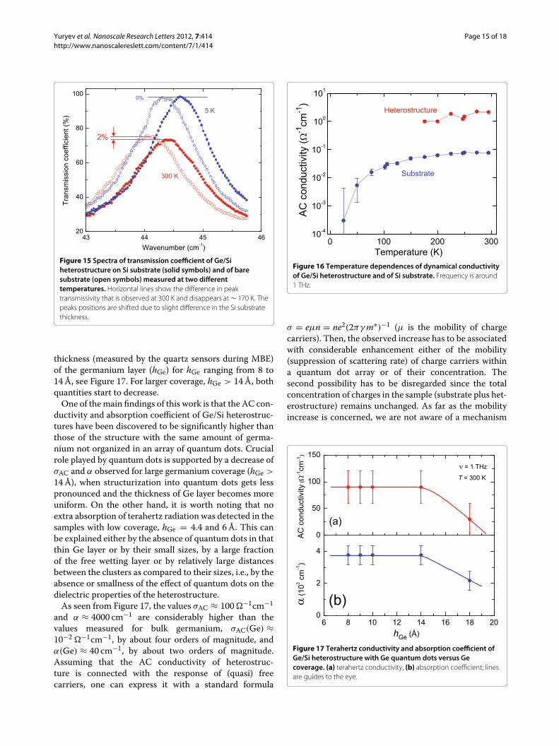
Influence of buffer layer thickness on photo-emf spectraAs seen from Figure 11, the buffer layer thickness deter-mines the QD layers position the in intrinsic domain andthus controls the relative position of the Fermi level andthe mini-band of the QD array in the region where the QDlayers are situated. The charge of the QD layer is deter-mined by the band occupation of the QD ensemble which,in turn, is controlled by the Fermi level location. For thisreason the effect of bias lighting on photo-emf generatedby the narrow-band radiation in the fundamental absorp-tion range is much stronger for the R 166 structure, whichhave a thick buffer layer, than for the R 163 one. This isclearly seen in Figure 12. The absolute value of photo-emf in the R 166 structure is lower than that in the R 163sample due to higher potential barriers for holes in thevalence band. Yet, the photo-emf response increases withthe growth of the bias lighting power much stronger in theR 166 p–i–n-diode than in the R 163 one.
Prospective photovoltaic IR detectorsOn the basis of our results on the photo-emf in the Si p–i–n-structures with Ge quantum dots, we have recently
Yuryev et al. Nanoscale Research Letters 2012, 7:414 Page 13 of 18http://www.nanoscalereslett.com/content/7/1/414
(a)
(b)
Figure 10 Photo-emf spectra of the p–i–n structures. (a) R 163:(1) without bias lighting; (2)–(5) under bias lighting (Ge filter):(2)W = 0.25mW/cm2; (3)W = 0.77mW/cm2; (4)W = 1.5mW/cm2;(5)W = 2.16mW/cm2; (b) R 166: (1) without bias lighting; (2)–(6)under bias lighting (Si filter): (2)W = 0.63mW/cm2;(3)W = 3.3mW/cm2; (4)W = 5.3mW/cm2; (5)W = 12mW/cm2;(6)W = 17.5mW/cm2.
proposed [39] a new design of photovoltaic quantumdot infrared photodetectors which enables detection ofvariations of photo-emf produced by the narrow-bandradiation in the Si fundamental absorption range (a refer-ence beam) under the effect of the wide-band IR radiationinducing changes in the Coulomb potential of the quan-tum dot ensemble which, in turn, affects the efficiency ofthe photovoltaic conversion of the reference beam. Thequantum dot array resembles a grid of a triode in thesedetectors which is controlled by the detected IR light.The reference narrow-band radiation generates a poten-tial between anode and cathode of this optically drivenquantum dot triode; a magnitude of this voltage dependson the charge of the QD grid (Figure 11). Such detec-tors can be fabricated on the basis of any appropriate
(a)
(b)
Figure 11 Schematics of band structures of the Si p–i–n-diodeswith Ge QD arrays represented in Figure 1. (a) R 163, (b) R 166;figures ‘1’, arrows and wavy lines indicate potential barriers for holesin the valence band (Ev) which are associated with the Ge QD arrays;black and shaded parts of potential wells show bands of filled (abovethe Fermi level F) and empty (below F) energy levels in the QDensemble; two vertical wavy lines in panel (b) indicate a gap in thedrawing of a very thick buffer layer of Si (1690 nm) deposited on then-Si substrate.
semiconductor structures with potential barriers, e.g., p–i–n-structures, p–n-junctions or Schottky barriers, andbuilt-in arrays of nanostructures.There are many ways to deliver the reference beam
to the detector, e.g., by irradiating the sensor by laseror LED. We propose, however, surface plasmon polari-tons delivered to the detector structures by the plasmonicwaveguides [40,41] to be applied as the reference beamsin the detector circuits. This approach makes such detec-tors, if based on Si, fully compatible with existing CMOSfabrication processes [42] that, in turn, opens a way todevelopment of plasmonic IR detector arrays on the basisof the monolithic silicon technology.
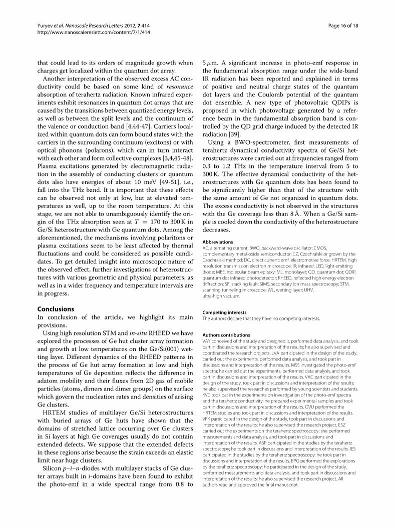
THz conductivity of multilayer Ge/Si QD arraysThe effective dynamic conductivity of Ge quantum dotlayer was determined bymeasuring the transmission coef-ficient spectra of heterostructures grown on Si(001) sub-strates. Characteristics of the substrates were determinedbeforehand as demonstrated by Figure 13 and Figure 14. InFigure 13, the interferometric pattern in the transmissioncoefficient spectrum Tr(ν) of a plane-parallel Si substrateis clearly seen. Pronounced dispersion of Tr(ν) peaks andtheir temperature dependence allow to extract the param-eters of the charge carriers (holes) by fitting the spectra
Yuryev et al. Nanoscale Research Letters 2012, 7:414 Page 14 of 18http://www.nanoscalereslett.com/content/7/1/414
0 1 2
68
101214161820222426
Phot
o-em
f(m
V)
Bias lighting power density (mW/cm2)
R 163
R 166
Figure 12 Dependence of photo-emf response of the R 163 andR 166 p–i–n-structures on bias lighting power density. Theexperimental conditions are the same as in Figure 10.
with Eq. (2) and by modelling the sample properties withthe Drude conductivity model where the complex ACconductivity is given by an expression [23,43]
σ ∗(ν) = σ1(ν) + iσ2(ν) = σ0γ 2
γ 2 + ν2+ i σ0νγ
γ 2 + ν2. (3)
Here σ1 is the real part and σ2 = ν(ε∞ −ε′)/2 is the imag-inary part of the conductivity, ε∞ is the high-frequencydielectric constant, σ0 = ν2pl/2γ is the DC conductiv-ity, ν2pl = (ne2/πm∗) 1
2 is the plasma frequency of thecarriers condensate, n, e and m∗ are, respectively, theirconcentration, charge and effective mass and γ is theirscattering rate. Figure 14 shows the temperature vari-ation of the plasma frequency and the scattering rateof charge carriers. Lowering of the plasma frequency ismainly connected with the carriers’ freezing out and theγ (T) behaviour is well described by a T− 3
2 dependence, asexpected.The values of effective dynamical conductivity and
absorption coefficient α = 4πk/λ of the heterostruc-tures with Ge quantum dots were determined basingon the measurements of terahertz transmission coeffi-cient spectra of the Si substrate with the heterostructureon it as compared to the spectra of the same substratewith the heterostructure etched away; this allowed usto avoid influence of (even slight) differences in dielec-tric properties of substrates cut of a standard commercialsilicon wafer. By comparing the so-measured transmis-sivity spectra we reliably detect, although small, changesin the amplitudes of interference maxima of a bare sub-strate caused by heterostructures. This is demonstratedby Figure 15: at T = 300K we clearly and firmly regis-ter a 2% lowering of the peak transmissivity introduced
Figure 13 Spectra of transmission coefficient of a siliconsubstrate (a commercial wafer, ρ = 12� cm), measured at twotemperatures using two different BWOworking in spectralranges from 11 cm−1 to 24 cm−1 and from 29 cm−1 to 39 cm−1.Dots show the measurement results, lines are least-square fits basedon the Drude conductivity model, as described in the text.
by the heterostructure. When cooling down, the differ-ence decreases and we were not able to detect it belowabout 170K, see Figure 16. Correspondingly, as is seenin Figure 16, the AC conductivity of the heterostructuredecreases while cooling, along with the conductivity of theSi substrate. The latter observation might be an indicationof the fact that the charges are delivered into the quan-tum dot array from the substrate; the statement, however,needs further exploration.Measuring the room temperature spectra, we have
found that the AC conductivity and the absorption coeffi-cient of the heterostructure do not depend on the effective
8
10
12
14
Pla
sma
freq
uenc
y (c
m-1) (a)
0 50 100 150 200 250 3000
10
20
30
40
50
Temperature (K)
Sca
tterin
gra
te (
cm-1)
~ T-3/2
(b)
Figure 14 Temperature dependences of the silicon substrateparameters obtained by fitting the transmission coefficientspectra as shown in Figure 13 and described in the text. (a)plasma frequency of charge carriers and (b) scattering rate. Solid linein (b) shows the T−3/2 behavior.
Yuryev et al. Nanoscale Research Letters 2012, 7:414 Page 15 of 18http://www.nanoscalereslett.com/content/7/1/414
Figure 15 Spectra of transmission coefficient of Ge/Siheterostructure on Si substrate (solid symbols) and of baresubstrate (open symbols) measured at two differenttemperatures. Horizontal lines show the difference in peaktransmissivity that is observed at 300 K and disappears at ∼ 170 K. Thepeaks positions are shifted due to slight difference in the Si substratethickness.
thickness (measured by the quartz sensors during MBE)of the germanium layer (hGe) for hGe ranging from 8 to14 A, see Figure 17. For larger coverage, hGe > 14 A, bothquantities start to decrease.One of themain findings of this work is that the AC con-
ductivity and absorption coefficient of Ge/Si heterostruc-tures have been discovered to be significantly higher thanthose of the structure with the same amount of germa-nium not organized in an array of quantum dots. Crucialrole played by quantum dots is supported by a decrease ofσAC and α observed for large germanium coverage (hGe >
14 A), when structurization into quantum dots gets lesspronounced and the thickness of Ge layer becomes moreuniform. On the other hand, it is worth noting that noextra absorption of terahertz radiation was detected in thesamples with low coverage, hGe = 4.4 and 6 A. This canbe explained either by the absence of quantum dots in thatthin Ge layer or by their small sizes, by a large fractionof the free wetting layer or by relatively large distancesbetween the clusters as compared to their sizes, i.e., by theabsence or smallness of the effect of quantum dots on thedielectric properties of the heterostructure.As seen from Figure 17, the values σAC ≈ 100�−1cm−1
and α ≈ 4000 cm−1 are considerably higher than thevalues measured for bulk germanium, σAC(Ge) ≈10−2 �−1cm−1, by about four orders of magnitude, andα(Ge) ≈ 40 cm−1, by about two orders of magnitude.Assuming that the AC conductivity of heterostruc-ture is connected with the response of (quasi) freecarriers, one can express it with a standard formula
Figure 16 Temperature dependences of dynamical conductivityof Ge/Si heterostructure and of Si substrate. Frequency is around1 THz.
σ = eμn = ne2(2πγm∗)−1 (μ is the mobility of chargecarriers). Then, the observed increase has to be associatedwith considerable enhancement either of the mobility(suppression of scattering rate) of charge carriers withina quantum dot array or of their concentration. Thesecond possibility has to be disregarded since the totalconcentration of charges in the sample (substrate plus het-erostructure) remains unchanged. As far as the mobilityincrease is concerned, we are not aware of a mechanism
Figure 17 Terahertz conductivity and absorption coefficient ofGe/Si heterostructure with Ge quantum dots versus Gecoverage. (a) terahertz conductivity, (b) absorption coefficient; linesare guides to the eye.
Yuryev et al. Nanoscale Research Letters 2012, 7:414 Page 16 of 18http://www.nanoscalereslett.com/content/7/1/414
that could lead to its orders of magnitude growth whencharges get localized within the quantum dot array.Another interpretation of the observed excess AC con-
ductivity could be based on some kind of resonanceabsorption of terahertz radiation. Known infrared exper-iments exhibit resonances in quantum dot arrays that arecaused by the transitions between quantized energy levels,as well as between the split levels and the continuum ofthe valence or conduction band [4,44-47]. Carriers local-ized within quantum dots can form bound states with thecarriers in the surrounding continuum (excitons) or withoptical phonons (polarons), which can in turn interactwith each other and form collective complexes [3,4,45-48].Plasma excitations generated by electromagnetic radia-tion in the assembly of conducting clusters or quantumdots also have energies of about 10 meV [49-51], i.e.,fall into the THz band. It is important that these effectscan be observed not only at low, but at elevated tem-peratures as well, up to the room temperature. At thisstage, we are not able to unambiguously identify the ori-gin of the THz absorption seen at T = 170 to 300K inGe/Si heterostructure with Ge quantum dots. Among theaforementioned, the mechanisms involving polaritons orplasma excitations seem to be least affected by thermalfluctuations and could be considered as possible candi-dates. To get detailed insight into microscopic nature ofthe observed effect, further investigations of heterostruc-tures with various geometric and physical parameters, aswell as in a wider frequency and temperature intervals arein progress.
ConclusionsIn conclusion of the article, we highlight its mainprovisions.Using high resolution STM and in-situ RHEED we have
explored the processes of Ge hut cluster array formationand growth at low temperatures on the Ge/Si(001) wet-ting layer. Different dynamics of the RHEED patterns inthe process of Ge hut array formation at low and hightemperatures of Ge deposition reflects the difference inadatom mobility and their fluxes from 2D gas of mobileparticles (atoms, dimers and dimer groups) on the surfacewhich govern the nucleation rates and densities of arisingGe clusters.HRTEM studies of multilayer Ge/Si heterostructures
with buried arrays of Ge huts have shown that thedomains of stretched lattice occurring over Ge clustersin Si layers at high Ge coverages usually do not containextended defects. We suppose that the extended defectsin these regions arise because the strain exceeds an elasticlimit near huge clusters.Silicon p–i–n-diodes with multilayer stacks of Ge clus-
ter arrays built in i-domains have been found to exhibitthe photo-emf in a wide spectral range from 0.8 to
5μm. A significant increase in photo-emf response inthe fundamental absorption range under the wide-bandIR radiation has been reported and explained in termsof positive and neutral charge states of the quantumdot layers and the Coulomb potential of the quantumdot ensemble. A new type of photovoltaic QDIPs isproposed in which photovoltage generated by a refer-ence beam in the fundamental absorption band is con-trolled by the QD grid charge induced by the detected IRradiation [39].Using a BWO-spectrometer, first measurements of
terahertz dynamical conductivity spectra of Ge/Si het-erostructures were carried out at frequencies ranged from0.3 to 1.2 THz in the temperature interval from 5 to300K. The effective dynamical conductivity of the het-erostructures with Ge quantum dots has been found tobe significantly higher than that of the structure withthe same amount of Ge not organized in quantum dots.The excess conductivity is not observed in the structureswith the Ge coverage less than 8 A. When a Ge/Si sam-ple is cooled down the conductivity of the heterostructuredecreases.
AbbreviationsAC, alternating current; BWO, backward-wave oscillator; CMOS,complementary metal-oxide semiconductor; CZ, Czochralski or grown by theCzochralski method; DC, direct current; emf, electromotive force; HRTEM, highresolution transmission electron microscope; IR; infrared; LED, light emittingdiode; MBE, molecular beam epitaxy; ML, monolayer; QD, quantum dot; QDIP,quantum dot infrared photodetector; RHEED, reflected high energy electrondiffraction; SF, stacking fault; SIMS, secondary ion mass spectroscopy; STM,scanning tunneling microscope; WL, wetting layer; UHV,ultra-high vacuum.
Competing interestsThe authors declare that they have no competing interests.
Authors contributionsVAY conceived of the study and designed it, performed data analysis, and tookpart in discussions and interpretation of the results; he also supervised andcoordinated the research projects. LVA participated in the design of the study,carried out the experiments, performed data analysis, and took part indiscussions and interpretation of the results. MSS investigated the photo-emfspectra; he carried out the experiments, performed data analysis, and tookpart in discussions and interpretation of the results. VAC participated in thedesign of the study, took part in discussions and interpretation of the results;he also supervised the researches performed by young scientists and students.KVC took pat in the experiments on investigation of the photo-emf spectraand the terahertz conductivity; he prepared experimental samples and tookpart in discussions and interpretation of the results. OVU performed theHRTEM studies and took part in discussions and interpretation of the results.VPK participated in the design of the study, took part in discussions andinterpretation of the results; he also supervised the research project. ESZcarried out the experiments on the terahertz spectroscopy; she performedmeasurements and data analysis, and took part in discussions andinterpretation of the results. ASP participated in the studies by the terahertzspectroscopy; he took part in discussions and interpretation of the results. IESparticipated in the studies by the terahertz spectroscopy; he took part indiscussions and interpretation of the results. BPG performed the explorationsby the terahertz spectroscopy; he participated in the design of the study,performed measurements and data analysis, and took part in discussions andinterpretation of the results; he also supervised the research project. Allauthors read and approved the final manuscript.
Yuryev et al. Nanoscale Research Letters 2012, 7:414 Page 17 of 18http://www.nanoscalereslett.com/content/7/1/414
AcknowledgementsThis research has been supported by the Ministry of Education and Science ofRF through the contracts No. 14.740.11.0069 and 16.513.11.3046 and by RFBRthrough the grant No. 11-02-12023-ofi-m. Equipment of the Center ofCollective Use of Scientific Equipment of GPI RAS was utilized for this study.We acknowledge the financial and technological support of this work.We express our appreciation to Ms. Natalya Kiryanova for her valuablecontribution to organization and management of this research.
Author details1A M Prokhorov General Physics Institute of RAS, 38 Vavilov Street, Moscow,119991, Russia. 2Technopark of GPI RAS, 38 Vavilov Street, Moscow, 119991,Russia. 3Moscow Institute of Physics and Technology, Institutsky Per. 9,Dolgoprudny, Moscow Region, 141700, Russia.
Received: 20 May 2012 Accepted: 16 June 2012Published: 23 July 2012
References1. Pchelyakov OP, Bolkhovitjanov YB, Dvurechenskii AV, Nikiforov AI,
Yakimov AI, Voigtlander B:Molecular beam epitaxy ofsilicon–germanium nanostructures. Thin Solid Films 2000,367:75.
2. Pchelyakov OP, Bolkhovitjanov YB, Dvurechenskii AV, Sokolov LV,Nikiforov AI, Yakimov AI, Voigtlander B: Silicon–germaniumnanostructures with quantum dots: Formation mechanisms andelectrical properties. Semicond 2000, 34:1229.
3. Yakimov AI, Dvurechenskii AV, Kirienko VV, Yakovlev YI, Nikiforov AI:Long-range Coulomb interaction in arrays of self-assembledquantum dots. Phys Rev B 2000, 61:10868.
4. Drexler H, Leonard D, Hansen W, Kotthaus JP, Petroff PM: Spectroscopyof quantum levels in charge-tunable InGaAs quantum dots. Phys RevLett 2252, 73:1994.
5. Lipparini E, Barberan N, Barranco M, Pi M, Serra L: Far-infrared edgemodes in quantum dots. Phys Rev B 1997, 56:12375.
6. Wang KL, Tong S, Kim HJ: Properties and applications of SiGenanodots.Materials Science in Semiconductor Processing 2005,8:389.
7. Wang KL, Cha D, Liu J, Chen C: Ge/Si self-assembled quantum dotsand their optoelectronic device applications. Proc of the IEEE 2007,95(9):1866.
8. Yakimov AI, Dvurechenskii AV, Nikiforov AI, Proskuryakov YY: InterlevelGe/Si quantum dot infrared photodetector. J Appl Phys 2001, 89:5676.
9. Arapkina LV, Yuryev VA: Classification of Ge hut clusters in arraysformed bymolecular beam epitaxy at low temperatures on theSi(001) surface. Phys Usp 2010, 53(3):279. [ArXiv:0907.4770].
10. Arapkina LV, Yuryev VA, Chizh KV, Shevlyuga VM, Storojevyh MS, KrylovaLA: Phase transition on the Si(001) clean surface prepared in UHVMBE chamber: A study by high resolution STM and in situ RHEED.Nanoscale Res Lett 2011, 6:218. [ArXiv:1009.3909].
11. Arapkina LV, Yuryev VA: CMOS compatible dense arrays of Gequantum dots on the Si(001) surface: Hut cluster nu-cleation,atomic structure, and array life cycle during UHVMBE growth.Nanoscale Res Lett 2011, 6:345. [ArXiv:1009.3831].
12. Yuryev VA, Arapkina LV: Ge quantum dot arrays grown by ultrahighvacuummolecular-beam epitaxy on the Si(001) surface: nucleation,morphology, and CMOS compatibility. Nanoscale Res Lett 2011, 6:522.[ArXiv:1104.2848].
13. Eltsov KN: Ultrahigh vacuum scanning tunneling microscope STMGPI-300. [http://surface.gpi.ru/papers/gpi300e.pdf].
14. Eltsov KN, Klimov AN, Kosyakov AN, Obyedkov OV, Shevlyuga VM, YurovVY: Ultrahigh vacuum scanning funnelling microscope GPI-300. InChemical state and atomic structure of fcc metal surfaces in chemicalreaction with halogens, Volume 59 of Proc. of General Physics Institute. Editedby Konov VI. Moscow, Russia, Nauka: Eltsov KN; 2003:45.
15. Yurov VY, Klimov AN: Scanning tunneling microscope calibration andreconstruction of real image: Drift and slope elimination. Rev SciInstrum 1994, 65:1551.
16. Horcas I, Fernandez R, Gomez-Rodriguez JM, Colchero J, Gomez-Herrero J,Baro AM:WSxM: A software for scanning probe microscopy and atool for nanotechnology. Rev Sci Instrum 2007, 78:013705.
17. Reinhardt KA, Kern W(Eds): Handbook of silicon wafer cleaning technology.2edition. Norwich, NY ,USA: William Andrew Inc.; 2008.
18. Arapkina LV, Shevlyuga VM, Yuryev VA: Structure and peculiarities ofthe (8 × n)-type Si(001) surface prepared in a molecular beamepitaxy chamber: A scanning tunneling microscopy study. JETP Lett2008, 87:215. [ArXiv:0908.1346].
19. Arapkina LV, Yuryev VA, Shevlyuga VM, Chizh KV: Phase transitionbetween (2 × 1) and c(8 × 8) reconstructions observed on theSi(001) surface around 600°C. JETP Lett 2010, 92(5):310.[ArXiv:1007.0329].
20. Kozlov G, Volkov A:Millimeter and submillimeter wave spectroscopyof solids. In Topics in Applied Physics, Volume 74. Edited by Gruner G.Berlin: Springer; 1998:51.
21. Gorshunov B, Volkov A, Spektor I, Prokhorov A, Mukhin A, Dressel M,Uchida S, Loidl A: Terahertz BWO-spectroscopy. Int J Infrared MillimeterWaves 2005, 26:1217.
22. Born M, Wolf E: Principles of Optics. London: Pergamon; 1959.23. Dressel M, Gruner G: Electrodynamics of Solids. London: Cambridge
University Press; 2002.24. Yuryev VA, Arapkina LV: Nucleation of Ge clusters at high
temperatures on Ge/Si(001) wetting layer. J Appl Phys 2012,111:094307. [ArXiv:1105.6012].
25. Arapkina LV, Yuryev VA: Nucleation of Ge quantum dots on the Si(001)surface. Phys Rev B 2010, 82:045315. [ArXiv:0907.4665].
26. Arapkina LV, Yuryev VA: An initial phase of Ge hut array formation atlow temperature on Si(001). J Appl Phys 2011, 109(10):104319.[ArXiv:1009.3831].
27. Goldfarb I, Hayden PT, Owen JHG, Briggs GAD: Nucleation of “hut” pitsand clusters during gas-source molecular-beam epitaxy ofGe/Si(001) in in situ scanning tunnelling microscopy. Phys Rev Lett1997, 78(20):3959.
28. Goldfarb I: Effect of strain on the appearance of subcritical nuclei ofGe nanohuts on Si(001). Phys Rev Lett 2005, 95:025501.
29. Yuryev VA, Arapkina LV: Defects of Ge quantum dot arrays on theSi(001) surface. Physica B 2009, 404:4719. [ArXiv:0908.0841].
30. Kucherenko IV, Vinogradov VS, Melnik NN, Arapkina LV, Chapnin VA, ChizhKV, Yuryev VA: Effect of interdiffusion and quantum confinement onRaman spectra of the Ge/Si(100) heterostructures with quantumdots. In Proceedings of the 16th International Symposium “Nanostructures:Physics and Technology”. Vladivostok, Russia: Ioffe Physico-TechnicalInstitute, St. Petersburg, Russia; 2008:199. [ArXiv:0908.1378].
31. Kucherenko IV, Vinogradov VS, Mel’nik NN, Arapkina LV, Chapnin VA,Chizh KV, Yuryev VA: The role of interdiffusion and spatialconfinement in the formation of resonant Raman spectra ofGe/Si(100) heterostructures with quantum-dot arrays. Phys SolidState 2008, 50:1970. [ArXiv:1010.1927].
32. Arapkina LV, Storozhevykh MS, Chapnin VA, Chizh KV, Uvarov OV,Kalinushkin VP, Yuryev VA: Ge/Si(001) heterostructures with densearrays of Ge quantum dots: Low-temperature formation,characterization by high resolution STM and TEM , and explorationof photo-EMF spectra. In Second International Symposium onNanotechnology, Energy and Space (“NES-2011”). Chernogolovka, MoscowRegion, Russia: Institute of Microelectronics Technology and High PurityMaterials of the Russian Academy of Sciences; 2011:32.
33. Storozhevykh MS, Arapkina LV, Chapnin VA, Kalinushkin VP, Chizh KV,Yuryev VA: Photosensitivity of Si p–i–n-structures with Ge quantumdots and effect of IR irradiation on its magnitude. In RussianConference and school on Actual Problems of SemiconductorPhotoelectronics (“Photonics-2011”). Edited by Aseev AL. Dvurechenskii AV ,Novosibirsk, Russia: A. V. Rzhanov Institute of Semiconductor Physics ofSiberian Brunch of the Russian Academy of Sciences; 2011:36.
34. Gerasimenko NN, Parhomenko YN: Silicon as aMaterial for Nanoelectronics.Moscow, Russia: Technosphera; 2007.
35. Brudnyi VN, Grinyaev SN, Dvurechenskii AV: Electronic properties ofsilicon with ultrasmall germanium clusters. Phys Solid State 2005,47(11):2020.
36. Talalaev VG, Cirlin GE, Tonkikh AA, Zakharov ND, Werner P, Gosele U,Tomm JW, Elsaesser T:Miniband-related 1.4–1.8μm luminescence ofGe/Si quantum dot superlattices. Nanoscale Res Lett 2006, 1:137.
37. Larsson M, Elfving A, Holtz PO, Hansson G, Ni WX: Photoluminescencestudy of Si/Ge quantum dots. Surf Sci 2003, 532-535:832.
Yuryev et al. Nanoscale Research Letters 2012, 7:414 Page 18 of 18http://www.nanoscalereslett.com/content/7/1/414
38. Talochkin AB, Chistokhin IB, Markov VA: Lateral photoconductivity ofmultilayer Ge/Si structures with Ge quantum dots. Semicond 2009,43(8):997.
39. Arapkina LV, Storozhevykh MS, Chizh KV, Chapnin VA, Yuryev:Method ofdetection of electromagnetic radiation and device for itsimplementation. Patent pending; Russian Federation Patent ApplicationNo. 2012122054May 29,2012 .
40. Bozhevolnyi SI, Volkov VS, Devaux E, Laluet JY, Ebbesen TW: Channelplasmon subwavelength waveguide components includinginterferometers and ring resonators. Nature 2006,440:508.
41. Holmgaard T, Chen Z, Bozhevolnyi SI, Markey L, Dereux A, Krasavin AV,Zayats AV: Bend- and splitting loss of dielectric-loaded surfaceplasmon-polariton waveguides. Optics Express 2008, 16(18):13585.
42. Krasavin AV, Zayats AV: Silicon-based plasmonic waveguides. OpticsExpress 2010, 18(11):11791.
43. Sokolov AV: Optical Properties of Metals. New York: American Elsevier; 1967.44. Heitmann D, Kotthaus JP: The spectroscopy of quantum dot arrays.
Phys Today 1993, 46:56.45. Boucaud P, Thanh VL, Sauvage S, Debarre D, Bouchier D: Intraband
absorption in Ge/Si self-assembled quantum dots. Appl Phys Lett1999, 74:401.
46. Weber A, Gauthier-Lafaye O, Julien FH, Brault J, Gendry M, Desieres Y,Benyattou T: Strong normal-incidence infrared absorption inself-organized InAs/InAlAs quantum dots grown on InP(001). ApplPhys Lett 1999, 74:413.
47. Sauvage S, Boucaud P, Gerard JM, Thierry-Mieg V: In-plane polarizedintraband absorption in InAs/GaAs self-assembled quantum dots.Phys Rev B 1998, 58:10562.
48. Hameau S, Isaia JN, Guldner Y, Deleporte E, Verzelen O, Ferreira R,Bastard G, Zeman J, Gerard JM: Far-infrared magnetospectroscopy ofpolaron states in self-assembled InAs/GaAs quantum dots. Phys Rev B2002, 65:085316.
49. Sikorski C, Merkt U: Spectroscopy of electronic states in InSb quantumdots. Phys Rev Lett 1989, 62:2164.
50. Dahl C, Kotthaus JP, Nickel H, Schlapp W: Coulomb coupling in arrays ofelectron disks. Phys Rev B 1992, 46:15590.
51. Demel T, Heitmann D, Grambow P, Ploog K: Nonlocal dynamicresponse and level crossing in quantum-dot structures. Phys Rev Lett1990, 64:788.
doi:10.1186/1556-276X-7-414Cite this article as: Yuryev et al.: Ge/Si(001) heterostructures with densearrays of Ge quantum dots: morphology, defects, photo-emf spectra andterahertz conductivity. Nanoscale Research Letters 2012 7:414.
Submit your manuscript to a journal and benefi t from:
7 Convenient online submission
7 Rigorous peer review
7 Immediate publication on acceptance
7 Open access: articles freely available online
7 High visibility within the fi eld
7 Retaining the copyright to your article
Submit your next manuscript at 7 springeropen.com


