Embed Size (px)
Citation preview

Graded TiAlN layers deposited by electron cyclotron resonance-assistedreactive sputtering
A. Raveha) and D. Z. RosenDivision of Chemistry, Nuclear Research Center–Negev, Beer-Sheva 84190, Israel
R. ShneckDepartment of Material Engineering, Ben-Gurion University, Beer-Sheva 84105, Israel
M. WeissDivision of Chemistry, Nuclear Research Center–Negev, Beer-Sheva 84190, Israel
~Received 4 December 1998; accepted 26 April 1999!
Graded TiAlN layers were deposited by plasma reactive sputtering assisted by electron cyclotronresonance~ECR!. For reactive sputtering, dual cathode radio-frequency magnetron targets, Ti andAl, were used. The layers were deposited using various combinations of variables such as powerinput, bias substrate voltage, and gas feed composition. The deposition process was monitored byoptical emission spectroscopy~OES!. The OES results indicate that microwave excitation added toradio-frequency plasma has contrasting effects on the Ti and Al concentration in the gas phase,enhancing titanium and quenching aluminum species reaching the deposited substrate. Thus, by theregulation of the ECR power and the ratio of nitrogen to argon flow, formation of graded layers ispossible. The layers formed in this way were characterized with regard to structure, composition,and mechanical properties using an x-ray diffractometer, an Auger electron spectroscopymicroscope, and a Vickers microhardness and scratch tester~for adhesion!. It was observed thatlayers deposited at a low ECR power~<100 W! yielded an oriented~111! crystalline structure withgood adhesion~failure load.70 N!. These layers displayed a higher microhardness~;25 GPa! atsubstrate bias voltage~;50 VDC! than that of a grounded substrate~10–15 GPa!. However, layersdeposited at an ECR power higher than 100 W showed a random or amorphous structure with anintermediate adhesion range~failure load of 30–50 N!. The relationship between the processingparameters, the structure, and the properties of the layers formed are presented and discussed.© 1999 American Vacuum Society.@S0734-2101~99!21004-4#
afoos
ah
blin
ut
i-pe
et
is
che
nd
mw
h-tus
AX
rat-
cessd totwoFig.tors
ofofoftionsedin
I. INTRODUCTION
TiAlN coating was found superior to other conventionbinary coatings such as TiN or AlN and fit to be usedcutting tools at significantly higher cutting speeds than thallowed for binary-coated tools.1,2
It was also reported that TiAlN showed improved weresistance and no apparent oxidation at a temperature asas 700 °C.3 The high oxidation resistance is due to the staaluminum oxide layer formed on top of the surface coatand it prevents further oxidation of the coated layer.4
TiAlN coatings have usually been prepared by variophysical vapor deposition processes, such as reactive spuing, ion plating, and arc processes.5–7
The composition of the reactive gas is critical for optimzation of the structure, microhardness, adhesion, cuttingformance, and oxidation behavior of TiAlN layers.8,9 Layerdeposition by reactive sputtering with two cathode targ~Ti and Al! assisted by electron cyclotron resonance~ECR!brings additional freedom to tailor film properties. Thisdue to the possibility to control the radio-frequency~rf!power of each cathode individually in addition to the effeof microwave~mw! excitation on the reactive gas and on tconcentration of the metal-nitride species.
a!Electronic mail: [email protected]
2001 J. Vac. Sci. Technol. A 17 „4…, Jul/Aug 1999 0734-2101/99/
lre
righeg
ster-
r-
s
t
In this article we describe the formation, structure, aproperties of a hard coating based on a~Ti, Al ! N systemusing dual-rf magnetron sputtering assisted by a ECRcoupled with rf bias.
II. EXPERIMENTAL PROCEDURES
TiAlN layers were produced by ECR-mw and rf tecniques in a setup that is shown in Fig. 1. The apparaconsists of an ECR-mw plasma source, Astex model4400~Applied Science and Technology Inc., Woburn, MA!,which is equipped with a magnet system capable of geneing a magnetic field of at least 875 G~lower limit! in thedesired plasma volume. The source is mounted on a prochamber, which contains the workpiece, and is connectea vacuum system. The apparatus was also equipped withsputter cathodes oriented 90° to each other, as shown in1. The sputter cathodes were operated with two rf genera~13.56 MHz!. One cathode target was Ti~99.99% purity!,and the other Al~99.9% purity!, both 3 in. in diameter and0.25 in. in thickness. This configuration allowed controlthe Ti and Al atom fluxes by changing the rf power inputeach target individually. In this way the deposition rateeach component was controlled separately. The rotaspeed of the substrate holder was 3 rpm. It may be rf biaup to21000 VDC. The sputtering process was conducted
200117 „4…/2001/6/$15.00 ©1999 American Vacuum Society

aas-l
15re
Cw
thix
pe
yeomN
te
ne
esic4a
vit
ndllo-was
est-hesfnalove
g antsthe
ure-
atethe
ri-aser,by
Titita-esn-
-
or
ter-ant,
onn-ies
wi
d
f
st,
h
2002 Raveh et al. : Graded TiAlN layers deposited by ECR-assisted reactive sputtering 2002
various gas mixtures of argon~99.999%! and nitrogen~99.999%! in a reactor which had been pumped down byturbomolecular pump coupled to a rotary pump to a bpressure of 231027 Torr before the gas mixture was introduced. The substrates—~100! oriented silicon and M2 steetools-were pre-sputtered by mw~600 W! and rf bias voltage~2300 VDC! in an argon plasma discharge at 5 mTorr formin prior to film deposition. The substrate temperaturesulting from the deposition process reached a maximum220 °C. Graded layers were produced by regulating the Epower and rf substrate bias voltage with a constant posupply of rf cathodes and/or by changing N2/~N21Ar! ratioduring the deposition process.
Optical emission spectroscopy~OES! was utilized duringthe deposition process in order to continuously determineconcentration of excited and ionized particles of the gas mture in the plasma layer~maximum 10 mm thick! that islayered on the surface of the substrate. The emission of stral lines of sputtered atoms reaching the surface, suchtitanium and aluminum, was measured in the plasma laThe plasma layer was focused on the entrance slit of a cputerized optical emission system. The spectra of Ar and2
were also monitored as a function of the process paramesuch as ECR power input~0–800 W!, rf power input of thetargets~150–450 W!, bias voltage~0 to 2300 VDC!, andN2/~N21Ar! flow ratio ~0–1 sccm!.
After the deposition process, the layer composition amicrostructure were determined by an Auger electron sptroscopy~AES! microscope~PHI model 590 A!, a scanningelectron microscope~SEM Philips 505!, and x-ray diffrac-tion ~XRD! with Cu Ka radiation~with a Philips PW 1720x-ray generator and PW 1390 channel control!. Auger depthprofiling was performed using a rastered beam of 4.0 kions. The sputtering rate during the depth profiling analywas 5 and 30 nm/min, as estimated using a 100-nm-thtantalum oxide standard, with the analysis area being340mm2. The atomic percent of each of the elements wcalculated from the AES results using elemental sensiti
FIG. 1. Schematic diagram of the ECR and rf plasma deposition systema dual cathode~Al and Ti! used in the experiments.
J. Vac. Sci. Technol. A, Vol. 17, No. 4, Jul/Aug 1999
e
-ofRer
e-
c-asr.-
rs,
dc-
Visk0sy
factors and values obtained for standard films of TiN aAlN. The thickness of the layers was measured in metagraphic cross sections by SEM and the deposition ratecalculated from the deposition time.
The adhesion of the layer was studied by the scratch ting unit, designed by the Laboratoire Suisse de RechercHorlogeres~LSRH!, Neuchatel, Switzerland, with loads o10–100 N. The tests were performed with an acoustic sigdetector in the form of an accelerometer mounted just abthe diamond stylus~a spherical tip radius of 200mm!.
The microhardness of the layer was measured usindiamond indenter with a load of 0.025 N. The measuremewere obtained on a Vickers scale. The microhardness oflayer was determined by the mean of at least five measments taken on the surface.
III. EXPERIMENTAL RESULTS AND DISCUSSION
A. Factors affecting the deposition of TiAlN
The process variables studied~ECR power, power of thecathodes, bias voltage, and N2 concentration in the gas flow!were found to have a different effect on the deposition rand on the composition and mechanical properties ofdeposited layer ~Table I!. The ECR-mw power andN2/~N21Ar! ratio were found to be the most important vaables for tailoring the graded layer. The ECR power wfound to affect the composition of both the plasma laymonitored by OES, and the deposited layer, analyzedAES analysis. At the low power range~<100 W! the micro-wave excitation added to the radio-frequency~2200 VDC!Ti1Ar or Al1Ar plasma had contrasting effects on theand Al concentrations in the gas phase, enhancing thenium species@Fig. 2~a!# and quenching the aluminum speci@Fig. 2~b!# reaching the deposited substrate. It is worth metioning that no optical emission of either Ti1 or Al1 ions wasidentified. Only emission of Ar1 was observed at a wavelength of 475 nm@see Fig. 2~a!#. The optical emission of Ti1
and Al1 ions was most probably masked by the argonnitrogen emissions~not shown!.
When ECR-mw power was added to the reactive sputing process, while all other parameters were kept constthe effect of the mw discharge dominated@see Fig. 2~a!#. Theaddition of mw to rf power clearly enhanced the ionizatiand excitation of Ar and Ti as well as reduced the Al cocentration in the plasma layer. The reduction of Al spec
th
TABLE I. Factors affecting the deposition of TiAlN.
Process variables Affected property Analysis metho
ECR-mw power Ti and Al concentrations in the OESplasma layer
rf power of cathodes Sputtering rates of Ti and Al Measurements ofilm thickness
rf bias voltage Structure and mechanical XRD, scratch teproperties Vickers hardness
f N2/ f (N21Ar) Structure, composition, and XRD, AES, scratc
mechanical properties test, Vickershardness

uem
orRas
na
y
w
to
ioeioth
cal
f
theAlattalhas
s
shen
may
if-on,
toionen-ela-man
bediose
)
s
2003 Raveh et al. : Graded TiAlN layers deposited by ECR-assisted reactive sputtering 2003
by the addition of mw is not well understood. It may be dto a decrease of the mean free path of the sputtered Al atohence, they do not reach the substrate surface. It is wnoting that this effect was dominant only at a low ECpower, while at power higher than 100 W Al emission wenhanced. The layers deposited at mw.100 W had an amor-phous structure, and the ratio of Ti to Al could not be cotrolled. We therefore concentrated on layer formationmw<100 W.
Figure 3 shows the deposition rate (dh/dt) of the nitridelayer versusf N2
/ f (N21Ar) and the Ti/Al ratio as measured bOES in the plasma layer~at 363.8 nm for Ti and at 394.6 nmfor Al !. It can be seen that the deposition rate decreasedthe increase in f N2
/ f (N21Ar) from 30 nm/min forf N2
/ f (N21Ar)50 to about 19 nm/min forf N2/ f (N21Ar)50.4.
The Ti/Al optical intensity ratio showed a trend similarthat observed for the deposition rate of the TiAlN layer~Fig.3!. The minima of the deposition rate and the Ti/Al ratwere achieved atf N2
/ f (N21Ar)50.4. The decrease in thdeposition rate depicted in Fig. 3 may indicate a transitfrom TiAl metal to a TiAl nitride layer. Such a decrease wi
FIG. 2. Optical emission spectra of rf plasma and ECR-mw plasma.~a! Arplus Ti plasma; ~b! Ar plus Al plasma. ECR power5100 W;rf bias voltage52100 VDC; rf power of the cathodes (Al and Ti5400W; gas pressure59 mTorr.
JVST A - Vacuum, Surfaces, and Films
s;th
-t
ith
n
an increase of the nitrogen flow rate up to a certain critivalue is well known.9–11 Lowering of the sputtering rate isusually related to ‘‘target poisoning,’’ namely, formation oa nitride layer on the target surface.12 In our opinion, thelatter process, if it occurs, is a minor factor, because ofhigh sputtering rate at a relatively high rf power of Ti andcathodes~;8 W/cm2!. The increase in the deposition ratef N2
/ f (N21Ar)>0.58 is unclear. It may be due to experimenerror; however a similar increase in the deposition ratebeen reported before.13
The TiAlN phase was formed atf N2/ f (N21Ar)>0.4, while
at a lower value Ti12xAl xN was formed withx,0.5, and ata higher value a layer withx.0.5 was formed, confirmed byAES depth profile analysis~Fig. 4!. Figure 4 depicts depthprofiles of a Ti0.8Al0.2N layer deposited on silicon substrateat f N2
/ f (N21Ar)50.25@Fig. 4~a!# of a Ti0.5Al0.5N layer depos-ited at f N2
/ f (N21Ar)50.4 @Fig. 4~b!# and of a Ti0.4Al0.6Nlayer deposited atf N2
/ f (N21Ar)50.58 @Fig. 4~c!#.It should be noted that the concentration of N in the film
is relatively independent of the nitrogen flow rate, while tTi/Al ratio in the films increases quite substantially with aincrease in the nitrogen flow rate. Several processesoccur at the same time:~i! the effect of N on the sputteringrate and on the species which are sputtered;~ii ! the reactionof N with Ti and Al in the gas phase that may lead to dferent concentrations of metal-nitride species. In additilong-lived nitrogen metastables may transfer their energymetal atoms. The latter effect may lead to a higher emissintensity, which may not necessarily reflect a higher conctration of metal atoms in the gas phase. However, a corrtion was observed between the composition of the plaslayer, measured byin situ OES analysis, and the compositioof the deposited layer measured by AES.14
On the basis of the deposition parameters descriabove, several graded layers of TiAlN having various ratof Ti to Al were deposited. An AES depth profile of thsurface after the deposition process~Fig. 5! revealed a highAl concentration~;55 at. %! and a low Ti concentration
FIG. 3. Deposition rate and the ratio of optical emission intensities of Ti~at363.8 nm! and Al ~at 394.6 nm! as a function of nitrogen content in the gafeed (f N2
/ f (N21Ar)). ECR power5100 W; rf bias voltage5250 VDC; rfpower of the Ti and Al cathodes5400 W; gas pressure59 mTorr.
-oota
o
hed
ow
yth
t athei-
on-tworingn
rve
eor
riti-
ual
e at
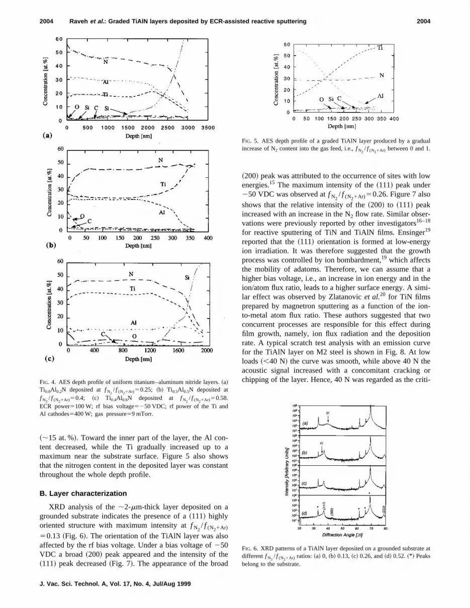
2004 Raveh et al. : Graded TiAlN layers deposited by ECR-assisted reactive sputtering 2004
~;15 at. %!. Toward the inner part of the layer, the Al content decreased, while the Ti gradually increased up tmaximum near the substrate surface. Figure 5 also shthat the nitrogen content in the deposited layer was consthroughout the whole depth profile.
B. Layer characterization
XRD analysis of the;2-mm-thick layer deposited on agrounded substrate indicates the presence of a~111! highlyoriented structure with maximum intensity atf N2
/ f (N21Ar)
50.13 ~Fig. 6!. The orientation of the TiAlN layer was alsaffected by the rf bias voltage. Under a bias voltage of250VDC a broad~200! peak appeared and the intensity of t~111! peak decreased~Fig. 7!. The appearance of the broa
FIG. 4. AES depth profile of uniform titanium–aluminum nitride layers.~a!Ti0.8Al0.2N deposited atf N2
/ f (N21Ar)50.25; ~b! Ti0.5Al0.5N deposited atf N2
/ f (N21Ar)50.4; ~c! Ti0.4Al0.6N deposited at f N2/ f (N21Ar)50.58.
ECR power5100 W; rf bias voltage5250 VDC; rf power of the Ti andAl cathodes5400 W; gas pressure59 mTorr.
J. Vac. Sci. Technol. A, Vol. 17, No. 4, Jul/Aug 1999
awsnt
~200! peak was attributed to the occurrence of sites with lenergies.15 The maximum intensity of the~111! peak under250 VDC was observed atf N2
/ f (N21Ar)50.26. Figure 7 alsoshows that the relative intensity of the~200! to ~111! peakincreased with an increase in the N2 flow rate. Similar obser-vations were previously reported by other investigators16–18
for reactive sputtering of TiN and TiAlN films. Ensinger19
reported that the~111! orientation is formed at low-energion irradiation. It was therefore suggested that the growprocess was controlled by ion bombardment,19 which affectsthe mobility of adatoms. Therefore, we can assume thahigher bias voltage, i.e., an increase in ion energy and inion/atom flux ratio, leads to a higher surface energy. A simlar effect was observed by Zlatanovicet al.20 for TiN filmsprepared by magnetron sputtering as a function of the ito-metal atom flux ratio. These authors suggested thatconcurrent processes are responsible for this effect dufilm growth, namely, ion flux radiation and the depositiorate. A typical scratch test analysis with an emission cufor the TiAlN layer on M2 steel is shown in Fig. 8. At lowloads~,40 N! the curve was smooth, while above 40 N thacoustic signal increased with a concomitant crackingchipping of the layer. Hence, 40 N was regarded as the c
FIG. 5. AES depth profile of a graded TiAlN layer produced by a gradincrease of N2 content into the gas feed, i.e.,f N2
/ f (N21Ar) between 0 and 1.
FIG. 6. XRD patterns of a TiAlN layer deposited on a grounded substratdifferent f N2
/ f (N21Ar) ratios:~a! 0, ~b! 0.13,~c! 0.26, and~d! 0.52.~* ! Peaksbelong to the substrate.

edth
eitrlaeas
e
fe
itro
ayersb-
t-
sitedr
rfom-tedas
inumma-
oo
as
sed
2005 Raveh et al. : Graded TiAlN layers deposited by ECR-assisted reactive sputtering 2005
cal load (Lc). At a load above 60 N the signal increasabruptly, indicating delamination and loss of cohesion ofcoating. This value was regarded as the failure load (L f).Table II shows theLc andL f as well as the thickness of thdeposited layers as a function of the bias voltage and ngen content in the gas phase. It can be seen that thedeposited at a constantf N2
/ f (N21Ar) on a grounded substratdisplayed better adhesion than that deposited on a bisubstrate. No correlation was found between theLc and thethickness of deposited layer which was similar in both typof substrate.
The nitrogen content in the gas phase was found to afthe surface microhardness of the deposited layer~Fig. 9!.The microhardness increased with the increase of the ngen concentration in the gas flow up to a value
FIG. 7. XRD patterns of TiAlN layer deposited on a biased~250 VDC!substrate at differentf N2
/ f (N21Ar) ratios: ~a! 0, ~b! 0.26, and~c! 0.52. ~* !Peaks belong to the substrate.
FIG. 8. Acoustic emission of a TiAlN layer deposited on an M2 steel tsubjected to different loads.
JVST A - Vacuum, Surfaces, and Films
e
o-yer
ed
s
ct
o-f
f N2/ f (N21Ar)'0.25 for both layers deposited on a250 VDC
biased substrate and on a grounded substrate. These lshowLc;30– 50 N. The layer formed on the grounded sustrate exhibited a lower microhardness~;15 GPa! comparedwith that formed on the250 VDC biased substrate and beter adhesion characteristics~Lc;50 GPa andL f>70 N!. Thedecrease of the surface microhardness of the layers depoat f N2
/ f (N21Ar)50.3 can be explained by the lower layethickness.
IV. CONCLUSIONS
Graded TiAlN layers were deposited by ECR-assistedreactive magnetron sputtering. It was observed that the cposition of the deposited layer and its structure were affecby a combination of a number of factors: mw power, bivoltage, and nitrogen content in the gas feed (f N2
/ f (N21Ar) ).Hence, the following was concluded.
~i! Microwave excitation ~<100 W! added to radio-frequency plasma enhances titanium and quenches alumspecies reaching the deposited substrate, allowing the fortion of graded TiAlN layers.
l
TABLE II. Adhesion and thickness of TiAlN layers as a function of bivoltage and nitrogen content (FN2
/ f (N21Ar)) in the gas feed.
Biasvoltage
~2VDC! f N2/ f (N21Ar)
Criticalload~N!
Failureload~N!
Thickness~mm!
0 0 10 30 3.60.13 50 70 2.80.26 45 60 2.40.39 20 30 2.10.52 20 30 2.5
50 0 50 70 3.50.26 30 55 2.40.52 40 50 2.2
FIG. 9. Microhardness of TiAlN layers deposited on grounded and bia~250 VDC! substrates vs nitrogen concentration in the gas phase.

o-o
a(rac
oke
Se
ec
.-D.
.-D.
ri,
in
d T.
r, J.
at.
2006 Raveh et al. : Graded TiAlN layers deposited by ECR-assisted reactive sputtering 2006
~ii ! High mw power excitation and/or bias voltage prduce high-energy ions, resulting in the formation of an amphous structure.
~iii ! Layers deposited at low ECR-mw power~<100 W!have an oriented~111! crystalline structure.
~iv! Layers deposited on a biased substrate are h~20–25 GPa! and have an intermediate adhesion rangeLc
;30– 50 N), while those deposited on a grounded substare less hard~10–15 GPa! and have better adhesion charateristics (Lc>70 N).
ACKNOWLEDGMENTS
The authors gratefully acknowledge the financial suppof the Israel Ministry of Science and the Arts, and would lito thank N. Bever for his expert technical assistance,Nathan for XRD analysis, and D. Imber for editing thmanuscript.
1W. Koing, R. Fritsch, and D. Kammermeier, Surf. Coat. Technol.49, 316~1991!.
2T. Leylendecker, O. Lemmer, S. Esser, and Ebberink, Surf. Coat. Tnol. 48, 175 ~1991!.
3W. D. Munz, J. Vac. Sci. Technol. A4, 2717~1991!.
J. Vac. Sci. Technol. A, Vol. 17, No. 4, Jul/Aug 1999
r-
rd
te-
rt
.
h-
4D. McIntyre, J. E. Greene, G. Hakansson, J. E. Sundgren, and WMunz, J. Appl. Phys.67, 1542~1990!.
5G. Hakansson, J.-E. Sundgren, D. McIntyre, J. E. Greene, and WMunz, Thin Solid Films153, 55 ~1987!.
6T. Suzuki, D. Huang, and Y. Ikuhara, Surf. Coat. Technol.107, 41~1988!.
7Y. Setsuhara, T. Suzuki, Y. Makino, S. Miyake, T. Sakata, and H. MoNucl. Instrum. Methods Phys. Res. B106, 120 ~1995!.
8O. Knotek, E. Elsing, M. Atzor, and H. G. Prengel, Wear133, 189~1989!.
9B.-Y. Shew, J.-L. Huang, and D.-F. Lii, Thin Solid Films293, 212~1997!.
10B.-Y. Shew and J.-L. Huang, Surf. Coat. Technol.71, 30 ~1995!.11S. Inoue, H. Uchida, A. Hioki, K. Koterazawa, and R. P. Howson, Th
Solid Films271, 15 ~1995!.12J. S. Morgan, W. A. Bryden, T. J. Kistenmacher, S. A. Ecelberger, an
O. Poehler, J. Mater. Res.5, 2677~1990!.13T. Ikeda and H. Satoh, Thin Solid Films195, 99 ~1991!.14A. Raveh, M. Weiss, and R. Shneck, Surf. Coat. Technol.111, 263
~1999!.15D. N. Lee, J. Mater. Sci.24, 4375~1989!.16R. Manory and G. Kimmel, Surf. Coat. Technol.63, 85 ~1994!.17A. J. Perry, C. Strandberg, W. D. Sproul, S. Hofmann, C. Ernsberge
Nickerson, and L. Chollet, Thin Solid Films153, 169 ~1987!.18K. T. Hyum, H. H. Joo, and B. H. Hahn, Surf. Coat. Technol.39–40, 409
~1989!.19W. Ensinger, Surf. Coat. Technol.65, 90 ~1994!.20M. Zlatanovic, R. Belosevac, N. Popovic, and A. Kunosic, Surf. Co
Technol.106, 150 ~1998!.


