Embed Size (px)
Citation preview
Journal of Crystal Growth 328 (2011) 5–12
Contents lists available at ScienceDirect
Journal of Crystal Growth
0022-02
doi:10.1
n Corr
E-m
journal homepage: www.elsevier.com/locate/jcrysgro
Growth of GaN epilayers on c-, m-, a-, and (20.1)-plane GaN bulk substratesobtained by ammonothermal method
M. Rudzinski a,n, R. Kudrawiec b, L. Janicki b, J. Serafinczuk c, R. Kucharski d, M. Zajac d, J. Misiewicz b,R. Doradzinski d, R. Dwilinski d, W. Strupinski a
a Institute of Electronic Materials Technology, Wolczynska 133, 01-919 Warsaw, Polandb Institute of Physics, Wroclaw University of Technology, Wybrzeze Wyspianskiego 27, 50-370 Wroc!aw, Polandc Faculty of Microsystem Electronics and Photonics, Wroclaw University of Technology, Janiszewskiego 11/17, 50-372 Wroc!aw, Polandd AMMONO sp. z.o.o., Czerwonego Krzyza 2/31, 00-377 Warsaw, Poland
a r t i c l e i n f o
Article history:
Received 8 December 2010
Received in revised form
8 June 2011
Accepted 13 June 2011
Communicated by T. Paskovaanalyzed. It was observed that the polishing of substrates and their misorientation have strong impact
Available online 28 June 2011
Keywords:
A1. MOCVD
A2. GaN
B1. X-ray diffraction
B2. Optical properties
48/$ - see front matter & 2011 Elsevier B.V. A
016/j.jcrysgro.2011.06.027
esponding author.
ail address: [email protected] (M
a b s t r a c t
GaN epilayers were grown by metalorganic chemical vapor deposition (MOCVD) on c-, m-, a-, and
(20.1)-plane GaN substrates obtained by the ammonothermal method. The influence of (i) the surface
preparation of substrates, (ii) MOCVD growth parameters, and (iii) the crystallographic orientation of
substrates on the structural and optical properties of GaN epilayers was investigated and carefully
on the quality of GaN epilayers grown on these substrates. The MOCVD growth process was optimized
for epilayers grown on m-plane GaN substrates. The best structural and optical properties were
achieved for epilayers deposited at 1075 1C and the total reactor pressure of 50 mbar. These conditions
were applied to grow GaN epilayers on substrates with other (c-, a-, and (20.1)-plane) crystallographic
orientations in the same MOCVD process. Particularly good optical properties were obtained for GaN
epilayers deposited on polar and non-polar (m- and a-plane) substrates, whereas slightly worse optical
properties were observed for epilayers deposited on the semi-polar substrate. It therefore means that
MOCVD growth conditions optimized for a given crystallographic direction (m-plane direction in this
case) work rather well also for other crystallographic directions.
& 2011 Elsevier B.V. All rights reserved.
1. Introduction
Recent progress in the growth of truly bulk GaN crystals by theammonothermal method [1] allows mass production of GaN sub-strates with various crystallographic orientations, including non-polar [2,3] and semi-polar substrates [4]. This indicates thatnowadays the growth of GaN-based devices can be developed forvarious crystallographic orientations but it is still unclear if thegrowth conditions, which are optimal for polar substrates, will besuitable for other crystallographic orientations. Moreover, it is ratherrarely discussed how critical is the preparation of the GaN surfacefor the growth of good quality epilayers. It should also be noted thatthis problem almost does not exist for GaN templates grown by theepitaxial methods on sapphire substrates since the surface is epi-ready just after the growth of such templates. In the case of GaNsubstrates sliced from a bulk boule, the proper surface preparationbefore the epitaxy is a real challenge. In addition, it was observedthat the substrate misorientation is a key parameter in the growthof good quality epilayers on non-polar GaN substrates [5–11].
ll rights reserved.
. Rudzinski).
Moreover, for polar GaN substrates it was perceived that thesubstrate misorientation influences the optical quality of depositedlayers, including the impurity incorporation, the alloy composition,and the surface morphology [12–14]. It means that the propersurface preparation before epitaxy (i.e., the quality of surfacepolishing and the proper substrate misorientation) is a key issuefor the epitaxy of GaN-based structures on truly bulk GaN substratesobtained by slicing from a bulk boule.
In this work we used truly bulk GaN substrates of variouscrystallographic orientations obtained by the ammonothermalmethod to grow GaN epilayers by metalorganic chemical vapordeposition (MOCVD). We focused on (i) the surface morphology ofepilayers deposited on GaN substrates of different surface quality, (ii)the optimization of growth process for m-plane GaN substrates, and(iii) the comparison of structural and optical properties of GaNepilayers grown simultaneously on c-, m-, a-, and (20.1)-plane GaNsubstrates at conditions optimized for m-plane GaN epilayers.
2. Experimental details
GaN substrates of various crystallographic orientations wereused for the epitaxy of GaN epilayers by MOCVD. These substrates

M. Rudzinski et al. / Journal of Crystal Growth 328 (2011) 5–126
were obtained by the ammonothermal method, which can beregarded as an analog of the commercially available hydrother-mal technology of a-quartz production in which a supercriticalaqueous solution can be used for chemical transport and re-crystallization of silicone dioxide. Relevant details on this growthmethod can be found in Ref. [1].
Table 1Definition of all polishing stages presented in this work.
Polishing stage Polishing type Sa (A) FWHM (arcsec)
#0 Rough 50 60–70
#1 Optical 1 30 �50
#2 Optical 2 10–20 30–40
#3 CMP 1 10–20 �25
#4 CMP 2 5–10 18–20
Fig. 1. DIM image of m-plane GaN substrates with 01 (left column) and 41 (right column
the polishing process (stages #0, #1, #2, and #4 from top to bottom).
The preparation of epi-ready GaN surface is not a simple taskbecause of the high hardness of GaN crystals and its unusualplastic properties leading to a large number of dislocationsgenerated by the stress, appearing during polishing, leading tothe creation of so-called subsurface damage layer (SDL). In thisrespect, the polishing process was performed by a combination ofmechanical polishing and chemical mechanical polishing (CMP).We used five different polishing stages labeled by numbers 0–4,from rough (0), through optical mechanically polished ones (1, 2)to the final, most precise, CMP polished surface (3, 4). Thepolishing stages can be distinguished by different kinds and sizesof abrasive grain, different mechanical pads, and different chemi-cals in final CMP processes. All these properly arranged steps areset to obtain a flat surface, free of visible polishing scratchesand SDL. Details about the parameters of each polishing stageare presented in Table 1. In general, two parameters were usedto define each step. The first one is Sa roughness parameter,measured by means of an Atos Micromap optical interferometer
) misorientation angle along the (0 0 0 1) direction obtained after various stages of

M. Rudzinski et al. / Journal of Crystal Growth 328 (2011) 5–12 7
in spatial range of 2.6 mm�2.9 mm. The second one is full widthat half maximum (FWHM) value of X-ray rocking curve measuredfor the polished surface by a Panalytical X’Pert Pro MRD high-resolution diffractometer with the following setup: Cu Ka1 line,U¼40 kV, I¼20 mA, 0.1 mm�0.1 mm slit for the incident beamand an open-detector mode for the diffracted beam. The FWHMvalue turned out to be highly sensitive to SDL thickness and wasused as an indirect way to probe it. It is worth stressing that themore precise was the polishing stage, the lower the Sa and FWHMvalues were obtained (see Table 1). The FWHM achieved afterstage #4 is very close to one of the ‘‘as-grown’’, unprocessedsurface of an AMMONO-GaN crystal, treated as the referencesurface from the point of view of lack of SDL. Therefore, the lastCMP stage is regarded as the process that finally removes SDL,together with polishing scratches, highly improving the surfacemorphology.
2-mm thick GaN epilayers were grown by MOCVD in a RFheated AIXTRON AIX-200 low pressure horizontal reactor.
Fig. 2. DIM image of m-plane GaN epilayers deposited on m-plane GaN substrates wi
direction obtained after various stages of the polishing process (stages #0, #1, #2, and
Trimethylgallium (TMGa) and ammonia (NH3) were used asprecursors and H2 as a carrier gas. In order to find optimal growthconditions GaN epilayers were deposited on both polar andunpolar GaN substrates at various temperatures and total pres-sures in the MOCVD reactor and V/III ratio equals 1000. Next GaNepilayers were deposited simultaneously in the same growthprocess on c-(Ga face), m-, a-, and (20.1)-plane GaN substrates.In this way, the influence of crystalographic orientation on thestructural and optical quality of GaN epilayers can be analyzed,neglecting differences, which could be related to some inaccura-cies in the repeating of the MOCVD process.
The optical properties of GaN epilayers were studied byphotoluminescence (PL) and reflectance in a system with a siliconCCD detector. For the PL measurements the samples were excitedby 266 nm line of an impulse YAG laser. For low temperaturemeasurements the samples were mounted on a cold finger in aclosecycle helium refrigerator. The structural properties wereinvestigated by high-resolution X-ray diffraction (XRD).
th 01 (left column) and 41 (right column) misorientation angle along the (0 0 0 1)
#4 from top to bottom).

M. Rudzinski et al. / Journal of Crystal Growth 328 (2011) 5–128
3. Results and discussion
Fig. 1 shows the differential interface microscopy (DIM) imageof m-plane GaN substrates with 01 (left column) and 41 (rightcolumn) misorientation angle along the (0 0 0 1) direction,obtained after various stages of the polishing process. Thepresented m-plane GaN substrates were used for the simulta-neous growth of GaN epilayers at conditions optimal for c-planeGaN layers (T¼1125 1C and the total pressure of 50 mbar in thereactor, and V/III ratio equals 1000). Fig. 2 presents the DIM imageof GaN epilayers grown on these substrates. Here, it is clearlyvisible that the morphology of GaN epilayers strongly depends onthe surface quality of m-plane GaN substrates. This morphology issingularly bad for epilayers deposited on poorly prepared sub-strates, see Fig. 2(a)–(c) and (e)–(g). When enhancing the processof surface preparation, the morphology of GaN epilayers improvessignificantly, see Fig. 2(d) and (h). In addition, it can also beobserved that the substrate misorientation influences the qualityof GaN epilayers (compare Fig. 2(d) with (h)), which indicates thatthe deposition of good quality m-plane GaN epilayers possiblyrequires an optimal misorientation of the substrate. It ought to behighlighted that the same polishing procedure applied to GaNsubstrates with a different misorientation angle does not guar-antee the same quality of the GaN surface. Moreover, quitesignificant differences in surface quality were observed whenthe same polishing process was applied to different crystallo-graphic orientations in GaN.
0.01
0.1
1
10
E II c
E _I_ c
unpol.
Ref
lect
ance
(arb
. u.)
PL
inte
nsity
(arb
. u.)
Ene3.3
83.4
03.4
23.4
43.4
63.4
83.5
03.5
23.3
83.4
03.4
23
0.01
0.1
1
10
CA, B
E II c
E _I_ c
unpol.
Ref
lect
ance
(arb
. u.)
PL
inte
nsity
(arb
. u.)
Energy (eV)
Fig. 3. Reflectance and photoluminescence spectra measured at 10 K in the vicinity of
and (c) 1125 1C.
Fig. 4. DIM image of m-plane GaN epilayers grown at various temperatures (a) 1025 1
The total reactor pressure was 50 mBar.
In order to optimize the MOCVD growth conditions it isimportant to eliminate the effect of substrate, which can beassociated with some differences in the quality of the surfacepolishing. In our case, we reduced/eliminated this effect bycutting large GaN substrates into smaller pieces after finalpolishing. Therefore, these substrates can be treated as identicalepi-ready substrates the quality of which is the same as thatshown in Fig. 1(d) and (h). We optimized the growth temperatureand the total pressure in the reactor. GaN layers were depositedon m-plane substrates with a few different misorientation angles(�11, 01, 11, and 41). Positive value of misorientation angledescribes off-cut along the (0 0 0 1) direction, and negative valuedescribes off-cut in the opposite direction.
In order to investigate the optical quality of GaN epilayers,both low temperature reflectance and the PL measurement wereperformed in the vicinity of excitonic transitions since the sharp-ness of exciton lines is particularly sensitive to the optical quality.
Fig. 3 shows the low temperature reflectance and the PLspectra of m-plane GaN epilayers grown at various temperatures.These epilayers were deposited on m-plane GaN substrates with�11 misorientation along the (0 0 0 1) direction. Firstly, it isworth noting here that some stacking faults (SFs) appear veryoften for GaN epilayers. Their presence is manifested in the PLspectra by an emission band at 3.42 eV. In our case, no emissionband was observed around this energy for the three GaN epi-layers, which proves that the number of SFs is negligibly small inour epilayers. To demonstrate the non-polar character of these
0.01
0.1
1
10
B CA
E II c
E _I_ c
Ref
lect
ance
(arb
. u.)
unpol.
PL
inte
nsity
(arb
. u.)
Energy (eV)
CB
A
rgy (eV)
.44 3.46
3.48
3.50
3.52
3.38
3.40
3.42
3.44
3.46
3.48
3.50
3.52
excitonic transitions for m-plane GaN epilayers grown at (a) 1025 1C, (b) 1075 1C,
C, (b) 1075 1C, and (c) 1125 1C on m-plane GaN substrates with 01 misorientation.

0
100000
200000
300000
-200 -100 0 100 2000
100000
200000
c-plane (00.2)m-plane (10.0)a-plane (11.0)(20.1)-plane (20.1)
c-plane (11.4)m-plane (20.1)a-plane (11.2)(20.1)-plane (20.0)
Inte
nsity
(arb
. u.)
Omega (sec.)
Fig. 5. X-ray rocking curves for symmetrical (a) and asymmetrical (b) reflections
for c-, m-, a-, and (20.1)-plane GaN epilayers.
M. Rudzinski et al. / Journal of Crystal Growth 328 (2011) 5–12 9
layers, the reflectance spectra were measured at the normalincidence with s( k?c, E:c)- and p( k?c, E?c)-polarization(where k and E are the light and electric field vectors, respec-tively, and ? and : represent perpendicular and parallel vectororientations). For unpolarized light three well resolved freeexciton transitions (A, B, and C) are observed in the reflectancespectrum at the energies of EA¼3.4776, EB¼3.4827, andEC¼3.5015 eV, which are typical of homoepitaxial epilayers[15,16]. The same exciton transitions appear when the electricvector is perpendicular to the c axis. But when the electric vectoris parallel to the c axis (p polarization) the A exciton is not presentin the reflectance spectrum. This observation confirms that ourcrystals have an ideal hexagonal symmetry without any localstructural imperfections, which could destroy this symmetry andchange the optical selection rules.
The narrowest exciton lines are observed in the reflectance spectraof the GaN epilayer grown at 1075 1C. Also for this epilayer narrowexcitonic lines are visible in the PL spectrum. It proves that theoptimal growth temperature is close to 1075 1C. For this temperaturewe grew GaN epilayers at various total pressures in the reactor. Weobtained a very similar optical quality for all epilayers grown atpressures reaching 200 mbar and hence we concluded that the mostcritical issue is the growth temperature. It is worth noting that thetemperature window for the growth of good quality m-plane GaNepilayers is quite narrow (we estimated that it could be �50 1C).Careful characterization of the optical quality was also performed forGaN epilayers deposited on m-plane substrates with the misorienta-tion angle of 01, 11, and 41. Finally, it was concluded that the optimalmisorientation angle is close to �11. However a rather good surfacemorphology, structural, and optical properties were also observed forepilayers deposited on m-plane GaN substrates without any misor-ientations (see the next part of this paper). A significantly worseoptical quality of GaN epilayers was noted when they were depositedon m-plane GaN substrates with 41 misorientation angle along the(0 0 0 1) direction. It suggests that the growth window stronglydepends on the misorientation angle.
Regarding the surface morphology of GaN layers deposited atvarious temperatures and pressures as well as substrates with adifferent surface misorientation we noticed that this morphologychanges between these, which are presented in Fig. 2(d) and (h).An example of DIM images for m-plane GaN epilayers obtained atvarious temperatures (i.e., epilayers with optical properties areshown in Fig. 3) is depicted in Fig. 4. In addition, we observed thatthe morphology of m-plane GaN epilayers is usually worse thanthe morphology of c-plane GaN epilayers grown under the sameconditions. Finally, we concluded that the temperature growthwindow of good quality m-plane GaN epilayers is narrower thanfor c-plane GaN epilayers and the growth of m-plane GaNepilayers with a good surface morphology and optical propertiesis more sensitive to the misorientation angle than the growth onc-plane GaN epilayers. In order to obtain m-plane surface withoutany terraces, the misorientation angle should be carefully opti-mized. Since the issue of atomic-like smoothes of the GaN surface(i.e., controlling of layer thickness with the monolayer accuracy)is extremely important in the growth of quantum wells, this issuewill be more carefully explored in the future. For the purpose ofthis work (i.e., the simultaneous growth of GaN epilayers on GaNsubstrates with various crystallographic orientations and com-parison of their structural and optical properties), the misorienta-tion angle of m-plane GaN substrate is optimized well enough forthe investigation of optimal MOCVD parameters, which could beapplied to other crystallographic orientations. Finally, we grewsimultaneously in one process c-, m-, a-, and (20.1)-plane GaNepilayers at the total reactor pressure of 50 mbar, at the tem-perature of 1075 1C on epi-ready GaN substrates without anymisorientation angle.
Fig. 5(a) and (b) show the rocking curves for symmetrical andasymmetrical reflections, respectively, for c-, m-, a-, and (20.1)-plane GaN epilayers. The narrowest peaks are observed for m- and(20.1)-plane epilayers. For c- and a-plane samples, XRD peaks areat least two times broader, which suggests worse structuralquality of these layers. In this work, due to its limited length,we decided only to indicate and present the comparison of FWHMof examined samples in one figure, at the same time showingsymmetric and asymmetric FWHM for each of them. We are wellaware that for all samples, the extent of FWHM broadening in theinstance of epitaxial layers on differently oriented crystals may becaused by various factors, the influence of which changesdepending on their quantity or ratio. Nevertheless, the compara-tive presentation of obtained results provides general informationon the quality of epitaxial layers grown on differently orientedGaN crystals obtained by the ammonothermal method. Structuralquality can be much better evaluated if we analyze the XRDreciprocal space maps, see Fig. 6. In this case, it is clearly visiblethat the a-plane epilayer is significantly worse, i.e., the symme-trical and asymmetrical peaks are not symmetric. It means thatsome structural imperfections are present in this layer. For the c-plane GaN epilayer, the broadening of XRD peaks is also muchlarger but these peaks are very symmetric. We suppose that largerbroadening of the XRD peak observed for the c-plane epilayershould be associated with a worse preparation of the GaNsubstrate before epitaxy [17]. In the case of the a-plane GaNepilayer, other effects such as the formation of point defects and/or dislocations can be more important than for m-plane epilayersand, therefore, the broadening of XRD peaks for this layer is largerthan for the m-plane layer. However, it should be stressed that forall the epilayers measured values for the full width half maximumof XRD peaks are very low (o50 arcsec) and constitute anoutstanding result that strongly indicates the excellent crystalline

c-plane (00.2) c-plane (11.4)
m-plane (10.0) m-plane (20.1)
a-plane (11.0) a-plane (11.2)
(20.1)-plane (20.1) (20.1)-plane (20.0)
Fig. 6. XRD reciprocal space maps for c-, m-, a-, and (20.1)-plane GaN epilayers.
M. Rudzinski et al. / Journal of Crystal Growth 328 (2011) 5–1210
properties of the studied material. For GaN epilayers grown onGaN templates or foreign substrates the FWHM of XRD peaks isusually a few times or even one magnitude larger.
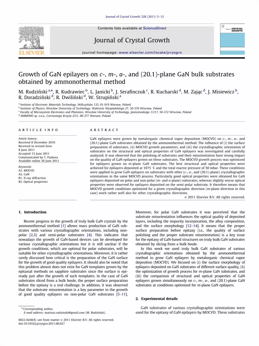
Fig. 7 shows reflectance and the PL spectra measured at 10 K inthe vicinity of excitonic transitions for GaN epilayers deposited onc-, m-, a- and (20.1)-plane GaN substrates. Firstly, the opticalquality of the m-plane epilayer grown on the GaN substratewithout any misorientation angle is comparable with the qualityof the epilayer deposited on the m-plane GaN substrate with �11misorientation angle, see Fig. 3(b). Moreover, it is clearly visiblethat the PL spectra are very similar in the case of GaN epilayersgrown on both polar and non-polar (m- and a-plane) substrates.The reflectance spectra are also alike for these epilayers but thec-plane GaN epilayer is not sensitive to the light polarization as
should be expected in this case. Some differences in reflectanceand the PL spectra (i.e., differences in the sharpness of spectralfeatures, which are related to excitonic transitions) are observedfor the epilayer grown on (20.1)-plane. In this case, excitonictransitions are not well resolved in reflectance as well as in the PLspectrum due to their larger broadening. It means that the opticalquality of this epilayer is worse than the quality of polar and non-polar layers but it should be emphasized that it still is rather goodsince free exciton transitions are also observed for this layer. Forpoor quality GaN layers such transitions should not be observedin reflectance and the PL spectra. For example, excitonic transi-tions were not noted for m-plane GaN epilayers shown inFig. 2(a)–(c) and (e)–(g). It should also be emphasized that anyspectral features, which could be related to SFs are not present in
0.1
1
10 K
CB
E II c
E _I_ c
Ref
lect
ance
(arb
. u.)
unpol.
A
PL
inte
nsity
(arb
. u.)
Energy (eV)
0.1
1
10 K
CB
E II c
E _I_ c
Ref
lect
ance
(arb
. u.)
unpol.
A
PL
inte
nsity
(arb
. u.)
Energy (eV)
0.1
1
10 K
CB
E II m
E _I_ m
Ref
lect
ance
(arb
. u.)
unpol.
A
PL
inte
nsity
(arb
. u.)
Energy (eV)3.3
83.4
03.4
23.4
43.4
63.4
83.5
03.5
23.3
83.4
03.4
23.4
43.4
63.4
83.5
03.5
23.3
83.4
03.4
23.4
43.4
63.4
83.5
03.5
23.3
83.4
03.4
23.4
43.4
63.4
83.5
03.5
2
0.1
1
CB
Ref
lect
ance
(arb
. u.)
unpol.
A10 K
PL
inte
nsity
(arb
. u.)
Energy (eV)
Fig. 7. Reflectance and photoluminescence spectra measured at 10 K in the vicinity of excitonic transitions for GaN epilayers grown on (a) c-plane, (b) m-plane, (c) a-plane,
and (d) (20.1)-plane GaN substrate.
M. Rudzinski et al. / Journal of Crystal Growth 328 (2011) 5–12 11
the case of four epilayers in the PL spectra in Fig. 7, which provesthat the number of SFs in GaN epilayers deposited on truly bulkGaN substrates is negligibly small. An important point to remem-ber is that the PL band at �3.95 eV (see Fig. 3(b) and Fig. 7(a)–(c))is not associated with SFs since it is the first LO phonon replica ofexcitonic transitions.
4. Summary
It has been shown that the proper preparation of ammo-nothermal GaN substrates is extremely important for the growthof high quality GaN epilayers. The substrate preparation includesboth the quality of the polishing process as well as the angle ofthe substrate misorientation in the proper direction. The MOCVDgrowth process was optimized for m-plane GaN substrates. Thebest quality m-plane GaN epilayers were obtained for the growthtemperature of 1075 1C and the total reactor pressure of 50 mbarand V/III ratio equals 1000. These conditions were applied to thesimultaneous growth of GaN epilayers on substrates with c-, m-,a-, and (20.1)-plane. Singularly good optical properties wereobserved for epilayers grown on polar and non-polar substrates.Slightly worse optical properties were noted for epilayers grownon semi-polar substrates. It means that the MOCVD growthconditions optimized for a given crystallographic direction (m-plane direction in this case) work rather well also for othercrystallographic directions. However, it is highly recommendedthat each growth direction should be optimized separately sincethe proper substrate misorientation can be of great importance inthis case. We believe that the small differences in structural andoptical properties observed by us appear due to the non-optimalsubstrate preparation/misorientation rather than the non-optimalMOCVD growth conditions for a given growth direction. Weexpect that the MOCVD growth conditions for different crystal-lographic orientations should be very similar, but the growthwindows can be narrower for some crystallographic directions.
Acknowledgments
This work was supported by the Polish Ministry of Scienceand Higher Education through Grant no. 6 ZR6 2009C/07280(‘‘Opracowanie i wdrozenie technologii produkcji niepolarnychpod"ozy GaN’’), National Center for Research and Development(Grant no. LIDER/14/192/L-1/09/NCBIR/2010), and the Ministry ofRegional Development (Grant no. POIG.01.01.02-00-015/09-00).
References
[1] R. Dwilinski, R. Doradzinski, J. Garczynski, L. Sierzputowski, R. Kucharski,M. Zajac, M. Rudzinski, R. Kudrawiec, J. Serafinczuk, W. Strupinski, J. Cryst.Growth 312 (2010) 2499.
[2] R. Kucharski, M. Rudzinski, M. Zajac, R. Doradzinski, J. Garczynski,L. Sierzputowski, R. Kudrawiec, J. Serafinczuk, W. Strupinski, R. Dwilinski,Appl. Phys. Lett. 95 (2009) 131119.
[3] R. Kudrawiec, M. Rudzinski, R. Kucharski, M. Zajac, R. Doradzinski,L.P. Sierzputowski, J. Garczynski, J. Serafinczuk, W. Strupinski, J. Misiewicz,R. Dwilinski, Phys. Status Solidi C 7 (2010) 2359.
[4] R. Kucharski, M. Zajac, R. Doradzinski, J. Graczynski, L. Sierzputowski,R. Kudrawiec, J. Serafinczuk, J. Misiewicz, R. Dwilinski, Appl. Phys. Express3 (2010) 101001.
[5] A. Hirai, Z. Jia, M.C. Schmidt, R.M. Farrell, S.P. DenBaars, S. Nakamura,J.S. Speck, K. Fujito, Appl. Phys. Lett. 91 (2007) 191906.
[6] H. Yamada, K. Iso, H. Saito, K. Fujito, S.P. DenBaars, S. Nakamura, Jpn. J. Appl.Phys. 46 (2007) L1117.
[7] H. Yamada, K. Iso, H. Masui, M. Saito, K. Fujito, S.P. DenBaars, S. Nakamura, J.Cryst. Growth 310 (2008) 4968.
[8] P. Misra, C. Boney, D. Starikov, A. Bensaoula, J. Cryst. Growth 311 (2009) 2033.[9] A. Strittmatter, J.E. Northrup, N.M. Johnson, M.V. Kisin, P. Spiberg,
H. El-Ghoroury, A. Usikov, A. Syrkin, Phys. Status Solidi B (2010).doi:10.1002/pssb.201046422.
[10] K.Y. Lai, T. Paskova, V.D. Wheeler, J.A. Grenko, M.A.L. Johnson, K. Udwary,E.A. Preble, K.R. Evans, J. Cryst. Growth 312 (2010) 902.
[11] R.M. Farrell, D.A. Haeger, X. Chen, M. Iza, A. Hirai, K.M. Kelchner, K. Fujito,A. Chakraborty, S. Keller, S.P. DenBaars, J.S. Speck, S. Nakamura, J. Cryst.Growth (2010). doi:10.1016/j.jcrysgro.2010.08.060.
[12] A.J. Ptak, T.H. Myers, L.T. Romano, C.G. Van de Walle, J.E. Northrup, Appl.Phys. Lett. 78 (2001) 285.
[13] S. Keller, N.A. Fichtenbaum, F. Wu, D. Brown, A. Rosales, S.P. DenBaars,J.S. Speck, U.K. Mishra, J. Appl. Phys. 102 (2007) 083546.

M. Rudzinski et al. / Journal of Crystal Growth 328 (2011) 5–1212
[14] T. Suski, E. Litwin-Staszewska, R. Piotrzkowski, R. Czernecki, M. Krysko,S. Grzanka, G. Nowak, G. Franssen, L.H. Dmowski, M. Leszczynski, P. Perlin,B. Łucznik, I. Grzegory, R. Jakie"a, Appl. Phys. Lett. 93 (2008) 172117.
[15] K.P Korona, A. Wysmo"ek, K. Paku"a, R. Stepniewski, J.M. Baranowski,I. Grzegory, B. Łucznik, M. Wroblewski, S. Porowski, Appl. Phys. Lett. 69(1996) 788.
[16] R. Kudrawiec, M. Rudzinski, J. Serafinczuk, M. Zajac, J. Misiewicz, J. Appl.Phys. 105 (2009) 093541.
[17] In this case the same polishing procedure was applied to all substrates. It wasobserved that the c-plane surface is the most difficult to polish, which meansthat the substrate with the c-plane has the worst quality in this set ofsubstrates.


