Embed Size (px)
Citation preview
HARDWARE MANUAL
ARM Cortex-A9 + FPGA CPU Module
DAVE Embedded Systems www.dave.eu [email protected]
ULTRA Line

B o r a H a r d w a r e M a n u a l v . 1 . 0 . 6
<Page intentionally left blank>
November, 2020 2/88
B o r a H a r d w a r e M a n u a l v . 1 . 0 . 6
Table of Contents1 Preface..................................................................................................................................6
1.1 About this manual..........................................................................................................61.2 Copyrights/Trademarks..................................................................................................61.3 Standards.......................................................................................................................61.4 Disclaimers....................................................................................................................61.5 Warranty.........................................................................................................................61.6 Technical Support..........................................................................................................71.7 Related documents........................................................................................................81.8 Conventions, Abbreviations, Acronyms.........................................................................8
2 Introduction.........................................................................................................................102.1 Product Highlights........................................................................................................122.2 Block Diagram..............................................................................................................132.3 Feature Summary........................................................................................................18
3 Design overview..................................................................................................................203.1 Xilinx Zynq™-7000 SoC..............................................................................................203.2 DDR3 memory bank....................................................................................................223.3 NOR flash bank...........................................................................................................223.4 NAND flash bank.........................................................................................................223.5 Integrated FPGA..........................................................................................................233.6 Memory Map................................................................................................................233.7 Power supply unit........................................................................................................233.8 CPU module connectors..............................................................................................24
4 Mechanical specifications...................................................................................................254.1 Board Layout................................................................................................................254.2 Connectors...................................................................................................................27
5 Power, reset and control.....................................................................................................285.1 Power Supply Unit (PSU) and recommended power-up sequence............................28
5.1.1 XCN15034 and power-off sequence....................................................................295.2 Reset............................................................................................................................31
5.2.1 MRST (J2.116)......................................................................................................325.2.2 PORSTn (J2.114).................................................................................................325.2.3 SYS_RSTn (J2.112).............................................................................................325.2.4 PS_MIO51_501 (J2.106)......................................................................................325.2.5 PS_MIO50_501 (J2.104)......................................................................................33
5.3 Voltage monitor............................................................................................................335.4 System boot.................................................................................................................33
5.4.1 Boot modes..........................................................................................................345.4.2 Default boot configuration....................................................................................355.4.3 Boot sequence customization..............................................................................35
5.5 Clock scheme..............................................................................................................365.6 Recovery......................................................................................................................36
November, 2020 3/88
B o r a H a r d w a r e M a n u a l v . 1 . 0 . 6
5.6.1 JTAG Recovery....................................................................................................365.6.2 SD/MMC Recovery...............................................................................................37
5.7 Multiplexing..................................................................................................................375.8 RTC..............................................................................................................................375.9 Watchdog.....................................................................................................................38
5.9.1 Selecting different configurations.........................................................................395.10 Thermal IC.................................................................................................................40
6 Pinout table.........................................................................................................................416.1 Carrier board mating connector J1..............................................................................426.2 Carrier board mating connector J2..............................................................................476.3 Carrier board mating connector J3..............................................................................52
7 Peripheral interfaces...........................................................................................................587.1 Notes on pin assignment.............................................................................................587.2 PS interfaces................................................................................................................59
7.2.1 Gigabit Ethernet....................................................................................................597.2.2 USB......................................................................................................................607.2.3 Quad-SPI..............................................................................................................617.2.4 Static memory controller (NAND).........................................................................617.2.5 I²C0.......................................................................................................................627.2.6 SD/SDIO...............................................................................................................627.2.7 UART1..................................................................................................................637.2.8 CAN......................................................................................................................637.2.9 JTAG.....................................................................................................................64
7.3 PL interfaces................................................................................................................647.3.1 FPGA Bank 34......................................................................................................667.3.2 FPGA Bank 35......................................................................................................69
7.3.2.1 Differential pairs...............................................................................................717.3.2.2 Single-ended signals........................................................................................717.3.2.3 FDDR_ADDR class..........................................................................................727.3.2.4 FDDR_CK class...............................................................................................747.3.2.5 FDDR_BYTE0 class.........................................................................................757.3.2.6 FDDR_BYTE1 class.........................................................................................767.3.2.7 VREF................................................................................................................777.3.2.8 Related Xilinx documentation..........................................................................77
7.3.3 FPGA Bank 13 (Zynq 7020 only).........................................................................788 Carrier board design guidelines..........................................................................................81
8.1 Suggested PCB specifications....................................................................................818.2 Power rails...................................................................................................................818.3 Main SD/MMC interface...............................................................................................828.4 Main Gigabit Ethernet interface (ETH0)......................................................................828.5 CAN interface...............................................................................................................828.6 XADC interface............................................................................................................83
November, 2020 4/88
B o r a H a r d w a r e M a n u a l v . 1 . 0 . 6
9 Operational characteristics.................................................................................................849.1 Maximum ratings.........................................................................................................849.2 Recommended ratings.................................................................................................849.3 Power consumption.....................................................................................................84
9.3.1 Testbed 1..............................................................................................................849.3.1.1 Results.............................................................................................................85
9.3.2 Testbed 2..............................................................................................................869.3.2.1 Results.............................................................................................................86
9.4 Heat Dissipation...........................................................................................................8710 Application notes...............................................................................................................88
Index of TablesTab. 1: Related documents.........................................................................................................8Tab. 2: Abbreviations and acronyms used in this manual...........................................................8Tab. 3: CPU, Memories, Buses.................................................................................................17Tab. 4: Peripherals....................................................................................................................17Tab. 5: FPGA specifications......................................................................................................18Tab. 6: Electrical, Mechanical and Environmental Specifications.............................................18Tab. 7: XC7-Z0x0 comparison..................................................................................................20Tab. 8: DDR3 specifications......................................................................................................21Tab. 9: NOR flash specifications...............................................................................................21Tab. 10: NAND flash specifications...........................................................................................22
Illustration IndexFig. 1: BORA – Powered by Zynq processor............................................................................10Fig. 2: BORA – Dual ARM Cortex A9 plus FPGA.....................................................................10Fig. 3: BORA SOM (top view)...................................................................................................12Fig. 4: Board layout - Top view..................................................................................................24Fig. 5: Board layout - Side view................................................................................................25Fig. 6: Connectors layout..........................................................................................................26
November, 2020 5/88
B o r a H a r d w a r e M a n u a l v . 1 . 0 . 6
1 Preface1.1 About this manual
This Hardware Manual describes the BORA CPU module design and functions.Precise specifications for the Xilinx Zynq processor can be foundin the CPU datasheets and/or reference manuals.
1.2 Copyrights/TrademarksEthernet® is a registered trademark of XEROX Corporation.All other products and trademarks mentioned in this manual areproperty of their respective owners.All rights reserved. Specifications may change any time without notification.
1.3 StandardsDAVE Embedded Systems is certified to ISO 9001 standards.
1.4 DisclaimersDAVE Embedded Systems does not assume any responsibility about availability, supplying and support regarding all the products mentioned in this manual that are not strictly part of the BORA CPU module.BORA CPU Modules are not designed for use in life support appliances, devices, or systems where malfunction of these products can reasonably be expected to result in personal injury.DAVE Embedded Systems customers who are using or selling these products for use in such applications do so at their own risk and agree to fully indemnify DAVE Embedded Systems forany damage resulting from such improper use or sale.
1.5 WarrantyBORA is warranted against defects in material and workmanshipfor the warranty period from the date of shipment. During the
November, 2020 6/88
B o r a H a r d w a r e M a n u a l v . 1 . 0 . 6
warranty period, DAVE Embedded Systems will at its discretion decide to repair or replace defective products. Within the warranty period, the repair of products is free of charge as long as warranty conditions are observed.The warranty does not apply to defects resulting from improper or inadequate maintenance or handling by the buyer, unauthorized modification or misuse, operation outside of the product’s environmental specifications or improper installation or maintenance.DAVE Embedded Systems will not be responsible for any defects or damages to other products not supplied by DAVE Embedded Systems that are caused by a faulty BORA module.
1.6 Technical SupportWe are committed to making our product easy to use and will help customers use our CPU modules in their systems. Technicalsupport is delivered through email to our valued customers. Support requests can be sent to [email protected] upgrades are available for download in the restricted access download area of DAVE Embedded Systems web site: http://www.dave.eu/reserved-area. An account is required to access this area and is provided to customers who purchase the development kit (please contact [email protected] for account requests).Please refer to our Web site at http://www.dave.eu/dave-cpu-module-zynq-bora.html for the latest product documentation, utilities, drivers, Product Change Notifications, Board Support Packages, Application Notes, mechanical drawings and additional tools and software.
November, 2020 7/88
B o r a H a r d w a r e M a n u a l v . 1 . 0 . 6
1.7 Related documentsDocument Location
DAVE Embedded Systems Developers Wiki
http://wiki.dave.eu/index.php/Main_Page
Zynq-7000 Technical Reference Manual
http://www.xilinx.com/support/documentation/user_guides/ug585-Zynq-7000-TRM.pdf
Zynq-7000 All Programmable SoC Packaging and Pinout
http://www.xilinx.com/support/documentation/user_guides/ug865-Zynq-7000-Pkg-Pinout.pdf
Tab. 1: Related documents
1.8 Conventions, Abbreviations, AcronymsAbbreviation DefinitionBELK BORA Embedded Linux Kit
FSBL First stage bootloader
GPI General purpose input
GPIO General purpose input and output
GPO General purpose output
PCB Printed circuit board
PL Zynq Programmable Logic
PS Zynq Processing System
RTC Real time clock
SOM System on module
TRM Technical Reference Manual
Tab. 2: Abbreviations and acronyms used in this manual
November, 2020 8/88
B o r a H a r d w a r e M a n u a l v . 1 . 0 . 6
Revision History
Version Date Notes
0.9.0 July 2013 First Draft
1.0.0 July 2013 First Release
1.0.1 May 2014 Updated block diagramUpdated pinout table
Updated Sections 5.1 and 5.2Updated Section 7 (MIO mapping, SD/
MMC, UART, I²C)Added info on differential pairsAdded “Carrier board design
guidelines” SectionMinor fixes
1.0.2 August 2014 Fixed PGOOD descriptionFixed power-up sequence diagram
Minor fixes
1.0.3 February 2015 Updated mechanical drawings for Rev.B SOM
Updated information onVDDIO_BANK13 pins
Minor fixes
1.0.4 September 2015 Added info on thermal ICMinor fixes
Released with BELK 2.2.0
1.0.5 March 2016 Updated watchdog and powersequence information
Minor fixesReleased with BELK 3.0.0
1.0.6 November 2020 Update Power Consumption and Heat dissipation
November, 2020 9/88
B o r a H a r d w a r e M a n u a l v . 1 . 0 . 6
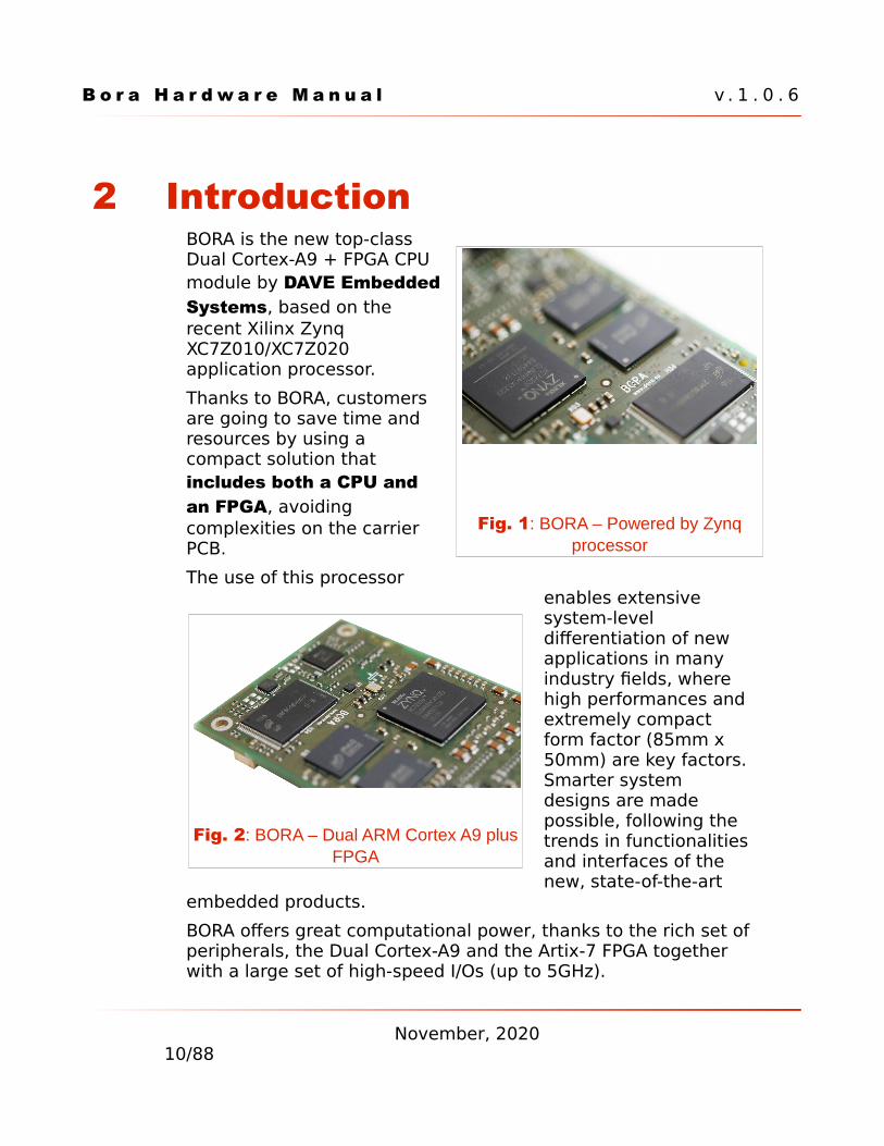
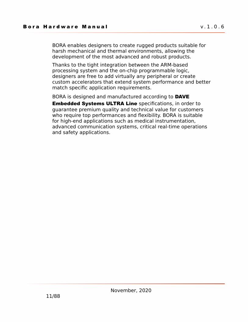
2 IntroductionBORA is the new top-classDual Cortex-A9 + FPGA CPUmodule by DAVE EmbeddedSystems, based on therecent Xilinx ZynqXC7Z010/XC7Z020application processor.
Thanks to BORA, customersare going to save time andresources by using acompact solution that includes both a CPU andan FPGA, avoidingcomplexities on the carrierPCB.
The use of this processorenables extensive system-level differentiation of new applications in many industry fields, where high performances and extremely compact form factor (85mm x 50mm) are key factors.Smarter system designs are made possible, following the trends in functionalitiesand interfaces of the new, state-of-the-art
embedded products.
BORA offers great computational power, thanks to the rich set ofperipherals, the Dual Cortex-A9 and the Artix-7 FPGA together with a large set of high-speed I/Os (up to 5GHz).
November, 202010/88
Fig. 1: BORA – Powered by Zynqprocessor
Fig. 2: BORA – Dual ARM Cortex A9 plusFPGA
B o r a H a r d w a r e M a n u a l v . 1 . 0 . 6
BORA enables designers to create rugged products suitable for harsh mechanical and thermal environments, allowing the development of the most advanced and robust products.
Thanks to the tight integration between the ARM-based processing system and the on-chip programmable logic, designers are free to add virtually any peripheral or create custom accelerators that extend system performance and bettermatch specific application requirements.
BORA is designed and manufactured according to DAVE Embedded Systems ULTRA Line specifications, in order to guarantee premium quality and technical value for customers who require top performances and flexibility. BORA is suitable for high-end applications such as medical instrumentation, advanced communication systems, critical real-time operations and safety applications.
November, 202011/88
B o r a H a r d w a r e M a n u a l v . 1 . 0 . 6
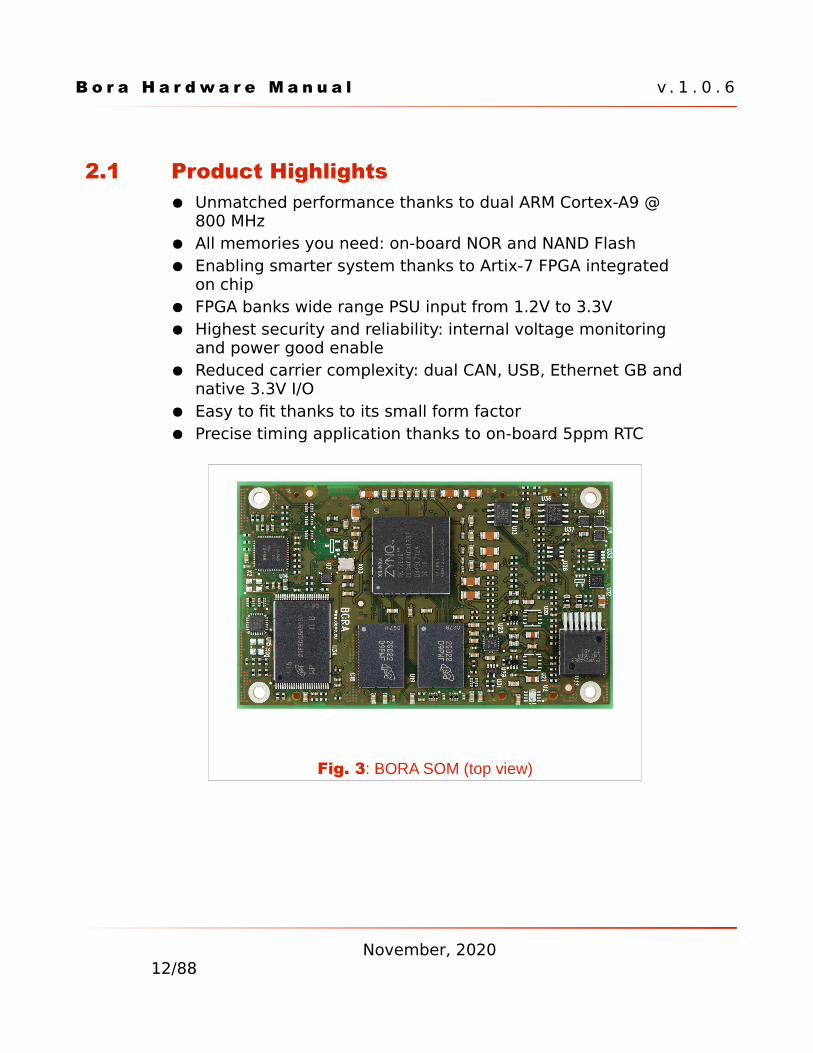
2.1 Product Highlights Unmatched performance thanks to dual ARM Cortex-A9 @
800 MHz All memories you need: on-board NOR and NAND Flash Enabling smarter system thanks to Artix-7 FPGA integrated
on chip FPGA banks wide range PSU input from 1.2V to 3.3V Highest security and reliability: internal voltage monitoring
and power good enable Reduced carrier complexity: dual CAN, USB, Ethernet GB and
native 3.3V I/O Easy to fit thanks to its small form factor Precise timing application thanks to on-board 5ppm RTC
November, 202012/88
Fig. 3: BORA SOM (top view)
B o r a H a r d w a r e M a n u a l v . 1 . 0 . 6
2.2 Block DiagramTo understand BORA block diagram it is necessary to briefly describe Zynq essential structure and routing scheme. For more details please refer to section 5.7 on page 37 where Xilinx's documentation references are listed.
Zynq is composed by two main blocks: the ARM Cortex-A9 dual-core subsystem – denoted as PS – and the FPGA subsystem – denoted as PL. Besides ARM processors, PS includes some native peripherals such as Gigabit Ethernet MAC controllers, USB controllers etc. PS is fully autonomous, meaning that, no matter if the PL is programmed, it is able to boot as if it was a traditional processor.
From the I/O standpoint, PS has several pads providing flexible multiplexing of native peripherals. These pads are denoted as MIOs and are grouped in some banks denoted as PS 50x.
November,2020
13/88
B o r a H a r d w a r e M a n u a l v . 1 . 0 . 6
November,2020
14/88
B o r a H a r d w a r e M a n u a l v . 1 . 0 . 6
November,2020
15/88
B o r a H a r d w a r e M a n u a l v . 1 . 0 . 6
On the other side, PL subsystem provides a lot of configurable I/Os, grouped in banks denotedas Bank x (eg Bank 9, Bank 13 etc.). Two types of such banks exist: HR1 and HP2.Some of the MIO signals can be routed outside the component via PL subsystem. This technique is called EMIO routing.
The block diagram shows the basic internal interconnections of BORA SoM.
On PS side, the following peripherals and devices are connected to MIO signals:
Serial NOR flash (MIO [6:1])
NAND flash (MIO [0], [14:2])
UART1 (MIO [49:48])
I2C temperature sensor (MIO [47:46])
I2C MEMS RTC (MIO [47:46])
Gigabit Ethernet PHY (MIO [27:16])
USBOTG PHY (MIO [39:28])
SD/MMC (MIO [45:40])
Since these devices are considered essential, they have been connected to MIO signals in order to make them always functional, even if PL is not programmed. These peripherals represent the default configuration for the BORA SOM, but other configurations can be implemented changing the pin multiplexing (please refer to section 5.7 on page 37).
Please note that serial NOR flash and NAND flash share some signals. Software drivers need to
1 HR: high range I/O with support for I/O voltage from 1.2V up to 3.3V.2 HP: high performance I/O with support for I/O voltage from 1.2V up to 1.8V.
November,2020
16/88
B o r a H a r d w a r e M a n u a l v . 1 . 0 . 6
properly handle this configuration to avoid misuse of these devices.
On PL side, the following devices are connected to I/O signals:
CAN transceiver (IO_L6P_T0_34, IO_L19P_T3_34).
Any of the CAN controllers of PS subsystem can be connected to CAN transceiver via EMIO routing with no limitations.
November,2020
17/88
B o r a H a r d w a r e M a n u a l v . 1 . 0 . 6
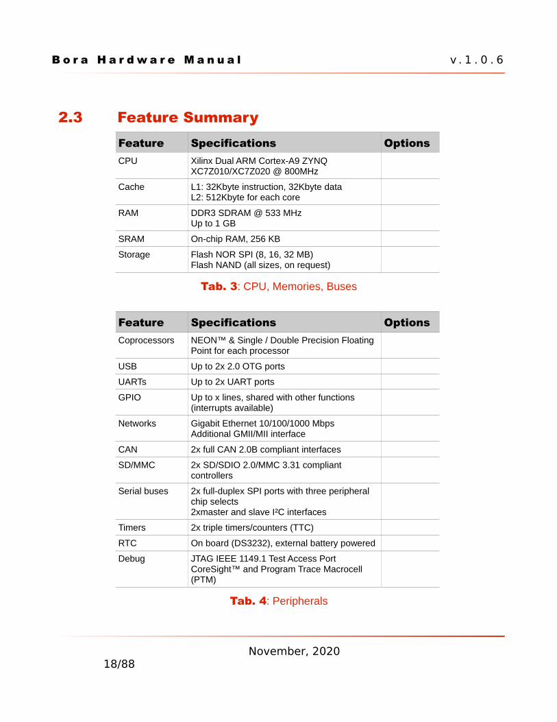
2.3 Feature SummaryFeature Specifications OptionsCPU Xilinx Dual ARM Cortex-A9 ZYNQ
XC7Z010/XC7Z020 @ 800MHz
Cache L1: 32Kbyte instruction, 32Kbyte dataL2: 512Kbyte for each core
RAM DDR3 SDRAM @ 533 MHzUp to 1 GB
SRAM On-chip RAM, 256 KB
Storage Flash NOR SPI (8, 16, 32 MB)Flash NAND (all sizes, on request)
Tab. 3: CPU, Memories, Buses
Feature Specifications OptionsCoprocessors NEON™ & Single / Double Precision Floating
Point for each processor
USB Up to 2x 2.0 OTG ports
UARTs Up to 2x UART ports
GPIO Up to x lines, shared with other functions (interrupts available)
Networks Gigabit Ethernet 10/100/1000 MbpsAdditional GMII/MII interface
CAN 2x full CAN 2.0B compliant interfaces
SD/MMC 2x SD/SDIO 2.0/MMC 3.31 compliant controllers
Serial buses 2x full-duplex SPI ports with three peripheral chip selects2xmaster and slave I²C interfaces
Timers 2x triple timers/counters (TTC)
RTC On board (DS3232), external battery powered
Debug JTAG IEEE 1149.1 Test Access PortCoreSight™ and Program Trace Macrocell (PTM)
Tab. 4: Peripherals
November, 202018/88
B o r a H a r d w a r e M a n u a l v . 1 . 0 . 6
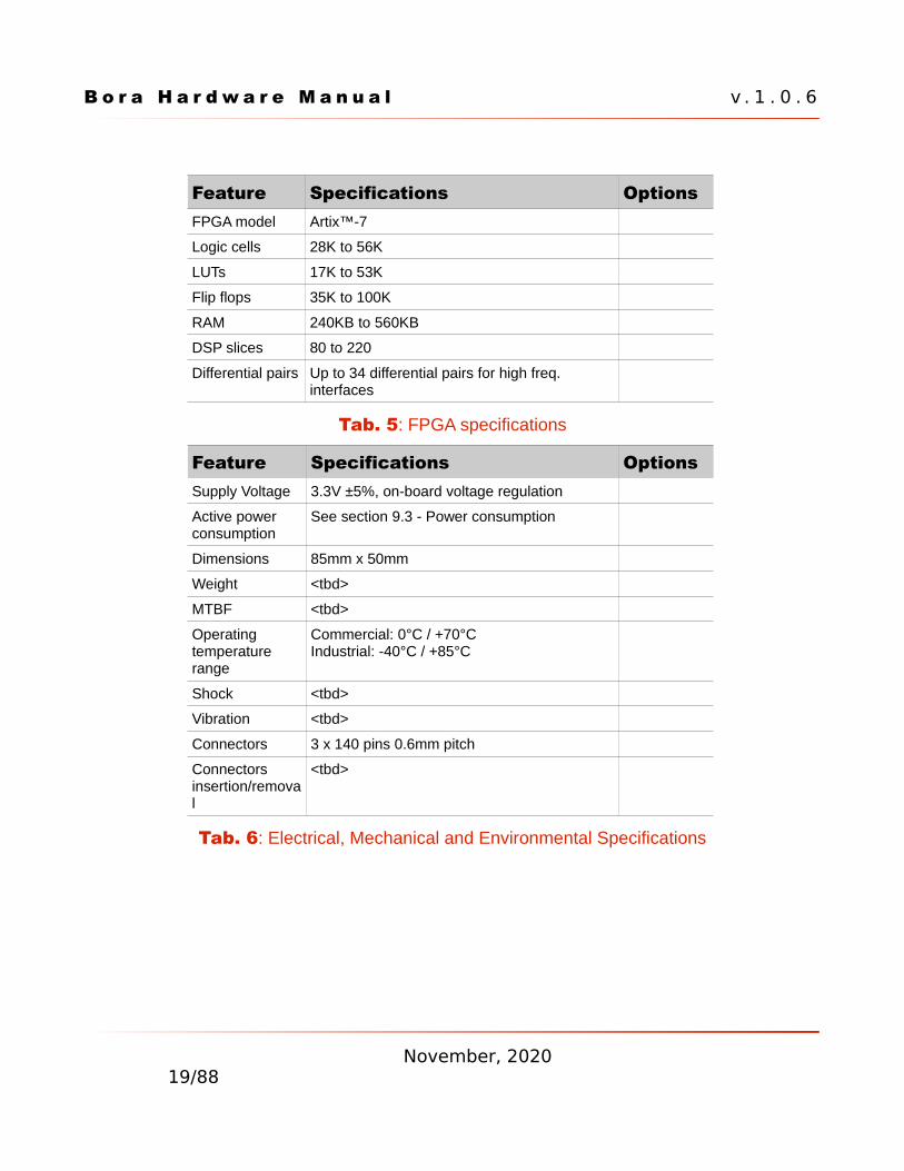
Feature Specifications OptionsFPGA model Artix™-7
Logic cells 28K to 56K
LUTs 17K to 53K
Flip flops 35K to 100K
RAM 240KB to 560KB
DSP slices 80 to 220
Differential pairs Up to 34 differential pairs for high freq. interfaces
Tab. 5: FPGA specifications
Feature Specifications OptionsSupply Voltage 3.3V ±5%, on-board voltage regulation
Active power consumption
See section 9.3 - Power consumption
Dimensions 85mm x 50mm
Weight <tbd>
MTBF <tbd>
Operating temperature range
Commercial: 0°C / +70°CIndustrial: -40°C / +85°C
Shock <tbd>
Vibration <tbd>
Connectors 3 x 140 pins 0.6mm pitch
Connectors insertion/removal
<tbd>
Tab. 6: Electrical, Mechanical and Environmental Specifications
November, 202019/88
B o r a H a r d w a r e M a n u a l v . 1 . 0 . 6
3 Design overviewThe heart of BORA module is composed by the following components:
Xilinx Zynq Z-7010 (XC7Z010) / Z-7020 (XC7Z020) SoC
Power supply unit
DDR memory banks
NOR and NAND flash banks
3x 140 pin connectors with interfaces signals
This chapter shortly describes the main BORA components.
3.1 Xilinx Zynq™-7000 SoCThe Zynq™-7000 family is based on the Xilinx Extensible Processing Platform (EPP) architecture. These products integratea feature-rich dual-core ARM® Cortex™-A9 based processing system (PS) and 28 nm Xilinx programmable logic (PL) in a single device. The ARM Cortex-A9 CPUs are the heart of the PS and also include on-chip memory, external memory interfaces, and a rich set of peripheral connectivity interfaces.
The Zynq-7000 family offers the flexibility and scalability of an FPGA, while providing performance, power, and ease of use typically associated with ASIC and ASSPs. The range of devices in the Zynq-7000 AP SoC family enables designers to target cost-sensitive as well as high-performance applications from a single platform using industry-standard tools. While each devicein the Zynq-7000 family contains the same PS, the PL and I/O resources vary between the devices. As a result, the Zynq-7000 AP SoC devices are able to serve a wide range of applications including:
Automotive driver assistance and driver information
Infotainment
Broadcast camera
Industrial motor control and industrial networking
November, 202020/88
B o r a H a r d w a r e M a n u a l v . 1 . 0 . 6
Machine vision
IP and Smart camera
LTE radio and baseband
Medical diagnostics and imaging
Multifunction printers
Video and night vision equipment
The Zynq-7000 AP SoC is composed of the following major functional blocks: Processing System (PS)
Application processor unit (APU)
Memory interfaces
I/O peripherals (IOP)
Interconnect
Programmable Logic (PL)
The processors in the PS always boot first, allowing a software centric approach for PL system boot and PL configuration. The PL can be configured as part of the boot process or configured at some point in the future. Additionally, the PL can be completely reconfigured or used with partial, dynamic reconfiguration (PR). PR allows configuration of a portion of the PL. This enables optional design changes such as updating coefficients or time-multiplexing of the PL resources by swapping in new algorithms as needed.
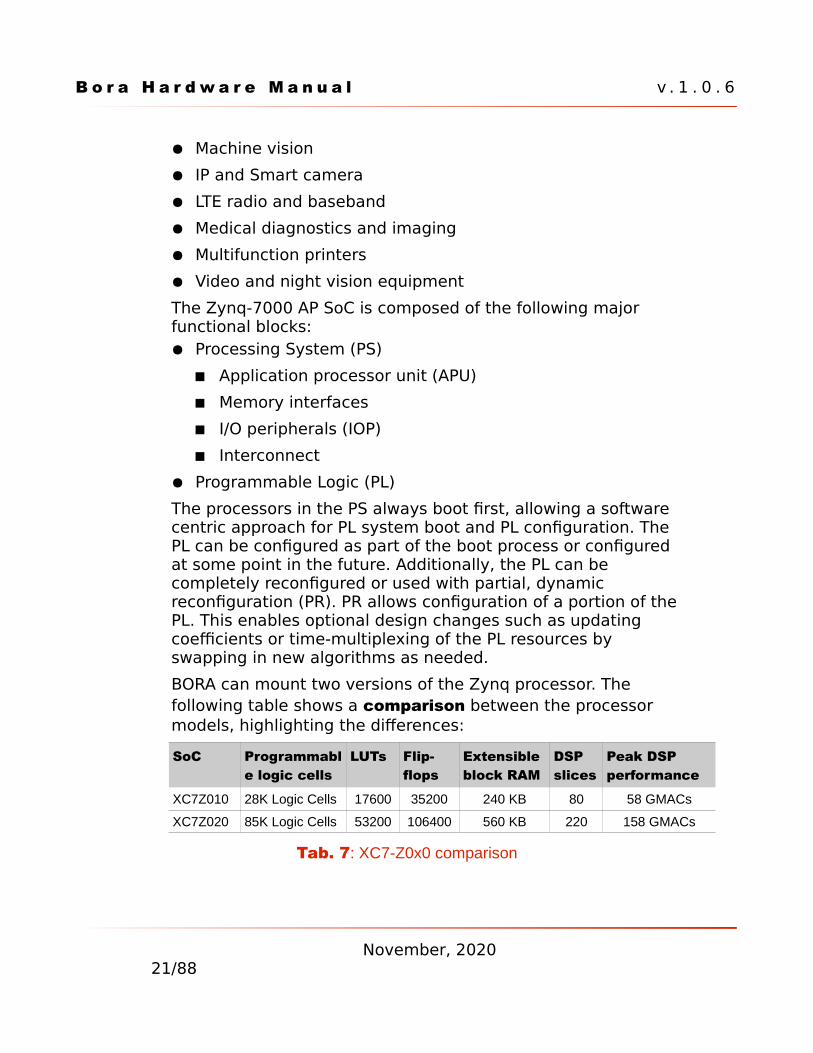
BORA can mount two versions of the Zynq processor. The following table shows a comparison between the processor models, highlighting the differences:
SoC Programmable logic cells
LUTs Flip-flops
Extensible block RAM
DSP slices
Peak DSP performance
XC7Z010 28K Logic Cells 17600 35200 240 KB 80 58 GMACs
XC7Z020 85K Logic Cells 53200 106400 560 KB 220 158 GMACs
Tab. 7: XC7-Z0x0 comparison
November, 202021/88
B o r a H a r d w a r e M a n u a l v . 1 . 0 . 6
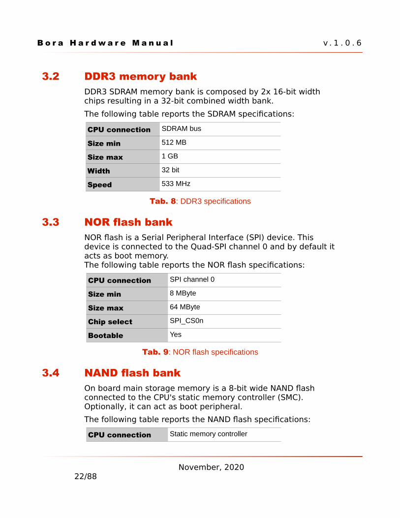
3.2 DDR3 memory bankDDR3 SDRAM memory bank is composed by 2x 16-bit width chips resulting in a 32-bit combined width bank.
The following table reports the SDRAM specifications:
CPU connection SDRAM bus
Size min 512 MB
Size max 1 GB
Width 32 bit
Speed 533 MHz
Tab. 8: DDR3 specifications
3.3 NOR flash bankNOR flash is a Serial Peripheral Interface (SPI) device. This device is connected to the Quad-SPI channel 0 and by default it acts as boot memory.The following table reports the NOR flash specifications:
CPU connection SPI channel 0
Size min 8 MByte
Size max 64 MByte
Chip select SPI_CS0n
Bootable Yes
Tab. 9: NOR flash specifications
3.4 NAND flash bankOn board main storage memory is a 8-bit wide NAND flash connected to the CPU's static memory controller (SMC). Optionally, it can act as boot peripheral.
The following table reports the NAND flash specifications:
CPU connection Static memory controller
November, 202022/88
B o r a H a r d w a r e M a n u a l v . 1 . 0 . 6
Page size 512 byte, 2 kbyte or 4 kbyte
Size min 128 MByte
Size max 2 GByte
Width 8 bit
Chip select NAND_CS0
Bootable Yes
Tab. 10: NAND flash specifications
3.5 Integrated FPGAThe PL is derived from Xilinx’s 7 Series FPGA technology (Artix™-7 for the 7z010/7z020). The PL is used to extend the functionality to meet specific application requirements. The PL provides many different types of resources including configurable logic blocks (CLBs), port and width configurable block RAM (BRAM), DSP slices with 25 x 18 multiplier, 48-bit accumulator and pre-adder (DSP48E1), a user configurable analog to digital converter (XADC), clock management tiles (CMT), a configuration block with 256b AES for decryption and SHA for authentication, configurable I/Os (with differential signaling capabilities). BORA customers are able to differentiate their product in hardware by customizing their applications using PL.
3.6 Memory MapFor detailed information, please refer to section “4.1 - Address Map” of the Zynq-7000 Technical Reference Manual.
3.7 Power supply unitBORA, as the other ULTRA Line CPU modules, embeds all the elements required for powering the unit, therefore power sequencing is self-contained and simplified. Nevertheless, powermust be provided from carrier board, and therefore users shouldbe aware of the ranges power supply can assume as well as all other parameters. For detailed information, please refer to
November, 202023/88
B o r a H a r d w a r e M a n u a l v . 1 . 0 . 6
Section 5.1.
3.8 CPU module connectorsAll interface signals BORA provides are routed through three 140pin 0.6mm pitch stacking connectors (named J1, J2 and J3). The dedicated carrier board must mount the mating connectors and connect the desired peripheral interfaces according to BORA pinout specifications.For mechanical information, please refer to Section 4 (Mechanical specifications). For pinout and peripherals information, please refer to Sections 6 (Pinout table) and 7 (Peripheral interfaces).
November, 202024/88
B o r a H a r d w a r e M a n u a l v . 1 . 0 . 6
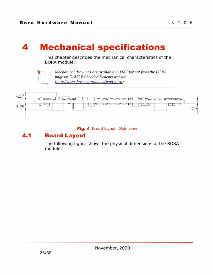
4 Mechanical specificationsThis chapter describes the mechanical characteristics of the BORA module.
Mechanical drawings are available in DXF format from the BORA page on DAVE Embedded Systems website (http://www.dave.eu/products/zynq-bora).
4.1 Board LayoutThe following figure shows the physical dimensions of the BORA module:
November, 202025/88
Fig. 4: Board layout - Side view
B o r a H a r d w a r e M a n u a l v . 1 . 0 . 6
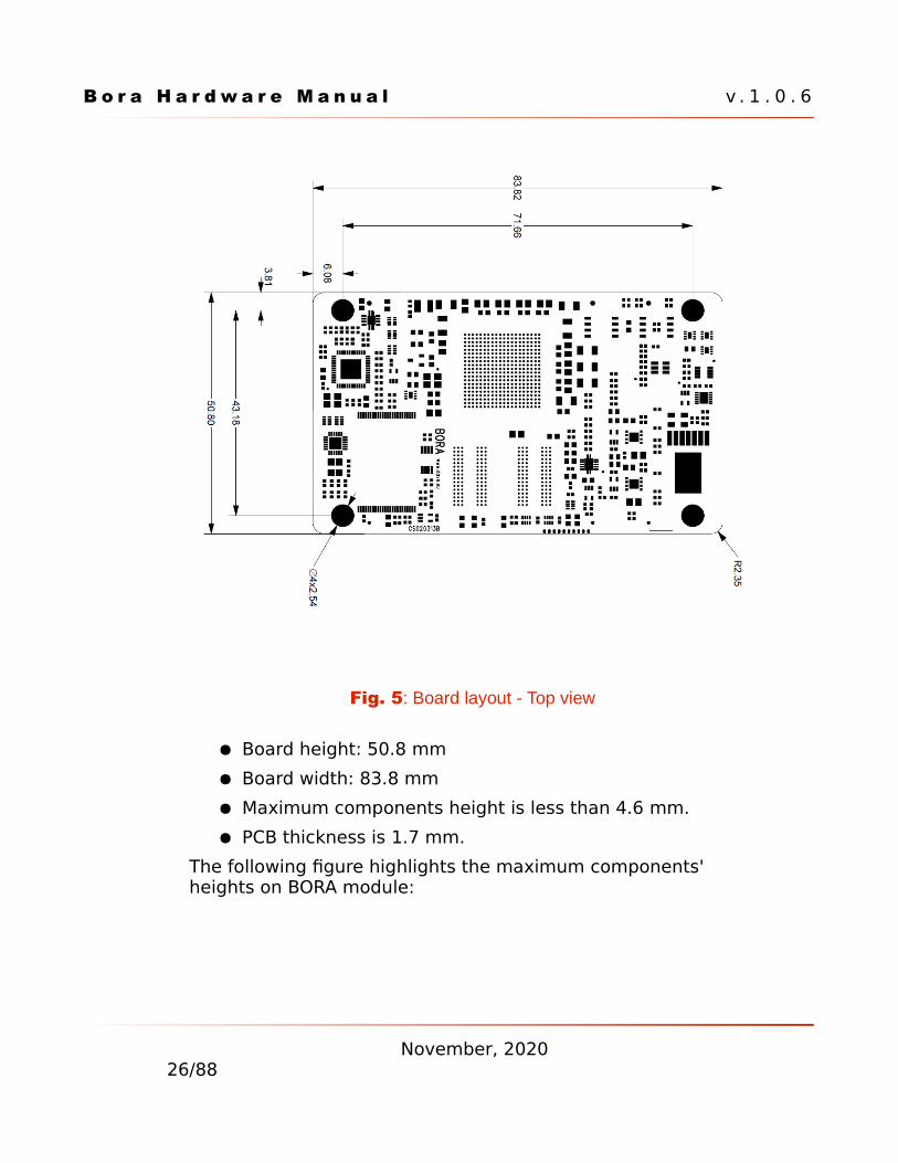
Board height: 50.8 mm
Board width: 83.8 mm
Maximum components height is less than 4.6 mm.
PCB thickness is 1.7 mm.
The following figure highlights the maximum components' heights on BORA module:
November, 202026/88
Fig. 5: Board layout - Top view
B o r a H a r d w a r e M a n u a l v . 1 . 0 . 6
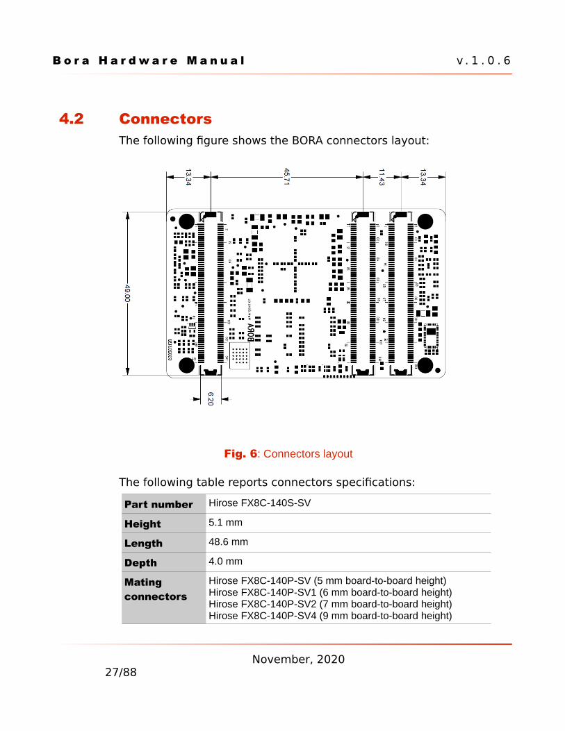
4.2 ConnectorsThe following figure shows the BORA connectors layout:
The following table reports connectors specifications:
Part number Hirose FX8C-140S-SV
Height 5.1 mm
Length 48.6 mm
Depth 4.0 mm
Mating connectors
Hirose FX8C-140P-SV (5 mm board-to-board height)Hirose FX8C-140P-SV1 (6 mm board-to-board height)Hirose FX8C-140P-SV2 (7 mm board-to-board height)Hirose FX8C-140P-SV4 (9 mm board-to-board height)
November, 202027/88
Fig. 6: Connectors layout
B o r a H a r d w a r e M a n u a l v . 1 . 0 . 6
Hirose FX8C-140P-SV6 (11 mm board-to-board height)
5 Power, reset and control 5.1 Power Supply Unit (PSU) and recommended
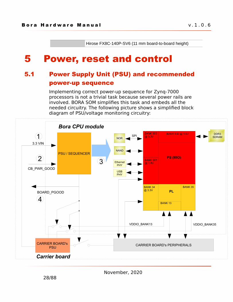
power-up sequenceImplementing correct power-up sequence for Zynq-7000 processors is not a trivial task because several power rails are involved. BORA SOM simplifies this task and embeds all the needed circuitry. The following picture shows a simplified block diagram of PSU/voltage monitoring circuitry:
November, 202028/88
Bora CPU module
Carrier board
3.3 VIN
CB_PWR_GOOD
PSU / SEQUENCER
CARRIER BOARD's PERIPHERALS
2
1
3
BOARD_PGOOD
BANK 34@ 3.3V
BANK 13
BANK 35
BANK 501@ 1.8V
BANK 500@ 3.3V
BANK 502 @ 1.5V
PS (MIO)
PL
EthernetPHY
USBPHY
DDR3SDRAM
NAND
NORSPI
CARRIER BOARD's PSU
VDDIO_BANK13 VDDIO_BANK35
4
B o r a H a r d w a r e M a n u a l v . 1 . 0 . 6
The recommended power-up sequence is:
1. main power supply rail (3.3VIN) ramps up
2. carrier board circuitry raises CB_PWR_GOOD; this indicates3.3VIN rail is stable3
3. BORA's PSU enables and sequences DC/DC regulators to turn circuitry on
4. BOARD_PGOOD signal is raised; this active-high signal indicates that SoM's I/O is powered. This signal can be used to manage carrier board power up sequence in order to prevent back powering (from SoM to carrier board or vice versa)
Please note that FPGA Bank 13 and FPGA Bank 35 of the PL must be powered by carrier board even if they are not used to implement any function. Two dedicated power rails are availablefor this purpose (VDDIO_BANK35 and VDDIO_BANK13) and offers the system designer the freedom to select the I/O voltageof these two banks. The power rails of both banks are enabled by the BOARD_PGOOD signal and are connected to the I/O power supply rail provided by the carrier board. Bora's PSU is designed to be robust against misbehaving power rails. However, the recommended power-on ramp for core and I/O supplies ranges from 1 to 6 V/ms.N.B.: Regarding power off, it is recommended that I/O supply is turned off before core supply.
5.1.1 XCN15034 and power-off sequenceOn 29th September 2015 Xilinx released a Product Change Notice indicating new power on/off requirements about Zynq components. A specific analysis has been undertaken with the help of Xilinx technical support to verify the compliance of BORAwith respect to the new requirements. This activity has led to the following recommendation: in order to prevent situations that might not fulfill such requirements, 3.3VIN off ramp speed must not exceed 50 V/ms. For more details on this topic, please refer to AR #65240
3 This step is not mandatory and CB_PWR_GOOD can be left floating. CB_PWR_GOOD is provided to prevent, if necessary, BORA's PSU to turn on during ramp of carrier board 3.3VIN rail. Depending on carrier board's PSU design, this may lead to undesired glitches during ramp-up.
November, 202029/88
B o r a H a r d w a r e M a n u a l v . 1 . 0 . 6
(http://www.xilinx.com/support/answers/65240.html) and XCN15034 (http://www.xilinx.com/support/documentation/customer_notices/xcn15034.pdf).
November, 202030/88
B o r a H a r d w a r e M a n u a l v . 1 . 0 . 6
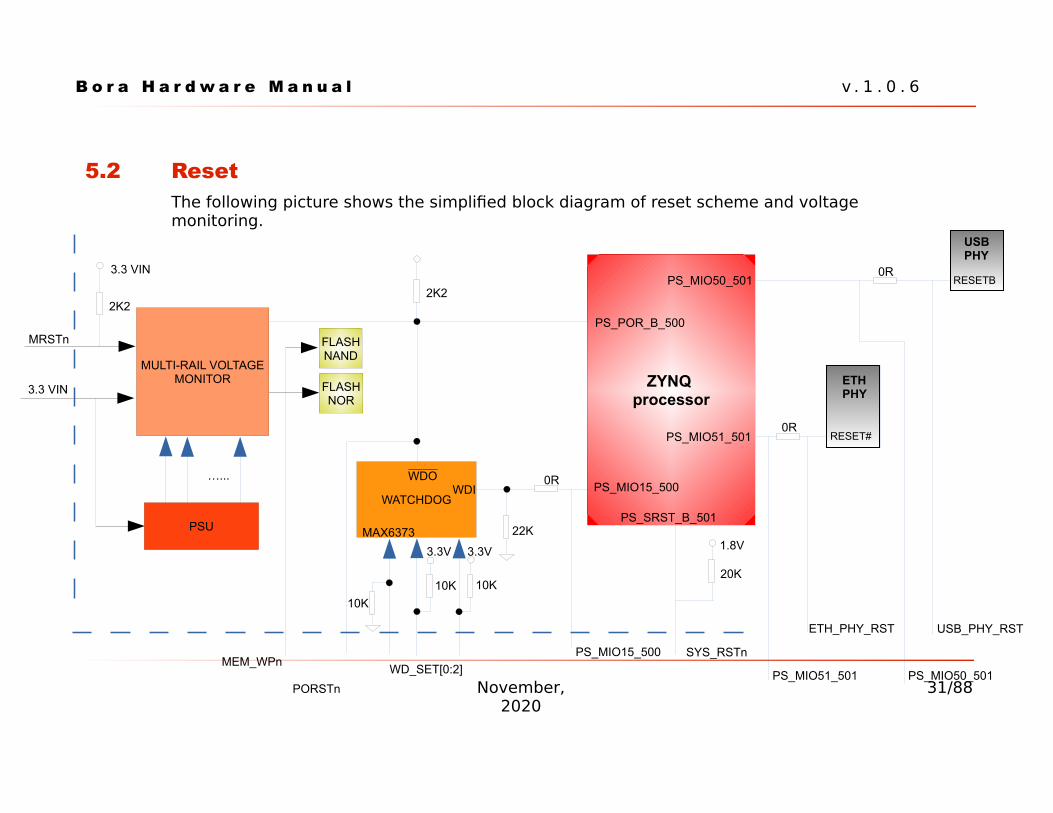
5.2 ResetThe following picture shows the simplified block diagram of reset scheme and voltage monitoring.
November,2020
31/88
ZYNQ processor
PS_SRST_B_501
FLASHNAND
FLASHNOR
WATCHDOG
MRSTn
3.3 VIN
PS_MIO15_500
PS_POR_B_500
3.3 VIN
2K2
MEM_WPn
PORSTn
WD_SET[0:2]
22K
0R
1.8V
20K
SYS_RSTn
WDIWDO
MAX6373
2K2
PSU
…...
MULTI-RAIL VOLTAGEMONITOR
PS_MIO15_500
PS_MIO51_501
PS_MIO50_501
RESET#
ETHPHY
0R
RESETB
USBPHY
0R
PS_MIO51_501
ETH_PHY_RST USB_PHY_RST
PS_MIO50_501
10K
10K 10K
3.3V 3.3V
B o r a H a r d w a r e M a n u a l v . 1 . 0 . 6
The available reset signals are described in detail in the following sections.
5.2.1 MRST (J2.116)MRSTn is a de-bounced input for manual reset (for example to connect a push-button). This signal connected to the voltage monitor and is pulled-up to 3.3VIN through a 2.2kOhm resistor.
5.2.2 PORSTn (J2.114)This is a bi-directional open-drain signal that is connected to Zynq's PS_SRST_B and can be asserted by the following devices:
a multi-rail voltage monitor that monitors 3.3VIN power rails and all of the rails generated by BORA's PSU. This monitor:
in case of a power glitch, asserts MEM_WPn signal in order to prevent any spurious write operation on flash memories too. MEM_WPn is 3.3V, push-pull, active low
has a timeout (set through an on-board capacitor) of about 200 ms
provides MRSTn de-bounced input for manual reset (for example to connect a push-button). Thissignal is pulled-up to 3.3VIN through a 2.2kOhm resistor
a watchdog timer (Maxim MAX6373). For more detailsplease refer to section 5.9 (Watchdog)
PORSTn is pulled-up to 3.3VIN through a 2.2kOhm resistor.
5.2.3 SYS_RSTn (J2.112)This signal is connected to Zynq's PS_SRST_B and is pulled-up to1.8V through a 20kOhm resistor.
5.2.4 PS_MIO51_501 (J2.106)By default, this signal is connected to on-board ETH PHY reset input. This allows complete software control of PHY reset sequence, even if FPGA is not programmed. In case this signals
November, 202032/88
B o r a H a r d w a r e M a n u a l v . 1 . 0 . 6
must be used to implement different functions on carrier board, alternative routing schemes are available on request in order to free this signal. For more details please refer to department sales.
5.2.5 PS_MIO50_501 (J2.104)By default, this signal is connected to on-board USB PHY reset input. This allows complete software control of PHY reset sequence, even if FPGA is not programmed. In case this signals must be used to implement different functions on carrier board, alternative routing schemes are available on request in order to free this signal. For more details please refer to department sales.
5.3 Voltage monitorThe voltage monitor is a Linear Technology LTC2930 (Configurable Six Supply Monitor with Adjustable Reset Timer, Manual Reset).
5.4 System bootThe boot process is multi-stage and minimally includes the Boot ROM and the first-stage boot loader (FSBL). The Zynq-7000 AP SoC includes a factory-programmed Boot ROM that is not user-accessible. The boot ROM:
determines whether the boot is secure or non-secure
performs some initialization of the system and clean-ups
reads the mode pins to determine the primary boot device
once it is satisfied, it executes the FSBL
After a system reset, the system automatically sequences to initialize the system and process the first stage boot loader fromthe selected external boot device. The process enables the user to configure the AP SoC platform as needed, including the PS and the PL. Optionally, the JTAG interface can be enabled to givethe design engineer access to the PS and the PL for test and
November, 202033/88
B o r a H a r d w a r e M a n u a l v . 1 . 0 . 6
debug purposes.
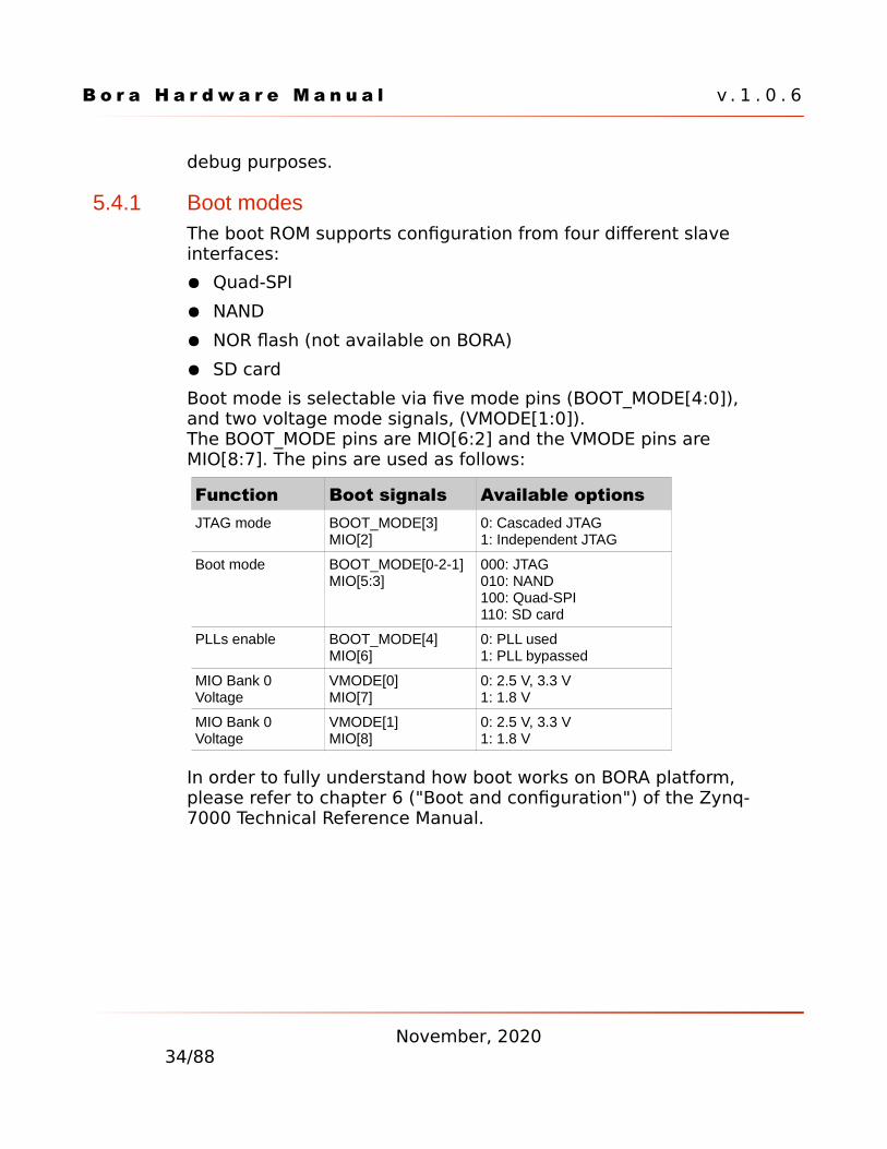
5.4.1 Boot modesThe boot ROM supports configuration from four different slave interfaces:
Quad-SPI
NAND
NOR flash (not available on BORA)
SD card
Boot mode is selectable via five mode pins (BOOT_MODE[4:0]), and two voltage mode signals, (VMODE[1:0]).The BOOT_MODE pins are MIO[6:2] and the VMODE pins are MIO[8:7]. The pins are used as follows:
Function Boot signals Available optionsJTAG mode BOOT_MODE[3]
MIO[2]0: Cascaded JTAG1: Independent JTAG
Boot mode BOOT_MODE[0-2-1]MIO[5:3]
000: JTAG010: NAND100: Quad-SPI110: SD card
PLLs enable BOOT_MODE[4]MIO[6]
0: PLL used1: PLL bypassed
MIO Bank 0 Voltage
VMODE[0]MIO[7]
0: 2.5 V, 3.3 V1: 1.8 V
MIO Bank 0 Voltage
VMODE[1]MIO[8]
0: 2.5 V, 3.3 V1: 1.8 V
In order to fully understand how boot works on BORA platform, please refer to chapter 6 ("Boot and configuration") of the Zynq-7000 Technical Reference Manual.
November, 202034/88
B o r a H a r d w a r e M a n u a l v . 1 . 0 . 6
5.4.2 Default boot configurationDefault configuration for BORA module is:
Mode[0..3] = 1000: Quad-SPI mode
Mode[4] = 0: PLL not bypassed
VCFG[0] = 0: 2.5V, 3.3V operations for bank 0
VCFG[1] = 1: 1.8 operations for bank 1
Assuming that:
default configuration is not changed,
there's a valid boot code programmed in SPI flash memory
the actual boot sequence performed by ARM core will be:
5. Bootrom is executed from internal ROM code memory
6. FSBL is copied from on-board NOR flash memory connected to SPI0port to on-chip SRAM by bootrom
7. FSBL is executed from on-chip SRAM
8. U-Boot bootloader (2nd stage) is copied by FSBL from NOR flash memory connected to Quad-SPI port to SDRAM
9. U-boot (2nd stage) is executed from SDRAM
If no boot code is available in SPI NOR flash, the bootrom tries JTAG peripheral booting.
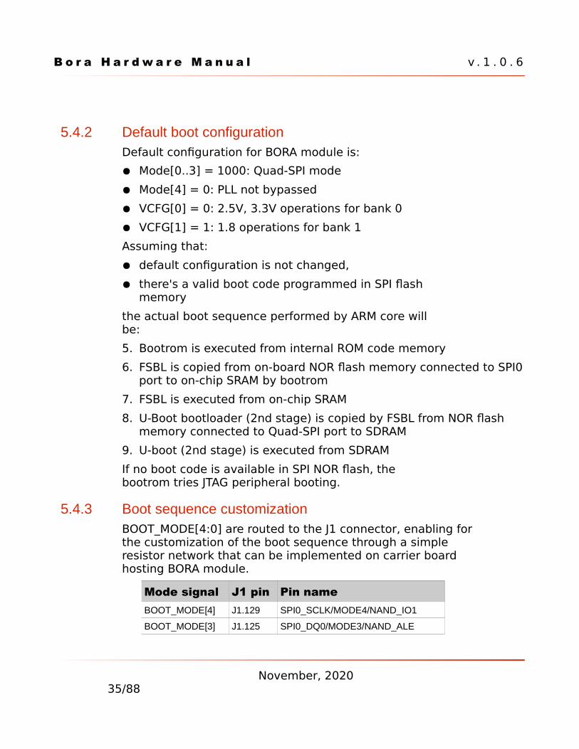
5.4.3 Boot sequence customizationBOOT_MODE[4:0] are routed to the J1 connector, enabling for the customization of the boot sequence through a simple resistor network that can be implemented on carrier board hosting BORA module.
Mode signal J1 pin Pin nameBOOT_MODE[4] J1.129 SPI0_SCLK/MODE4/NAND_IO1
BOOT_MODE[3] J1.125 SPI0_DQ0/MODE3/NAND_ALE
November, 202035/88
B o r a H a r d w a r e M a n u a l v . 1 . 0 . 6
Mode signal J1 pin Pin nameBOOT_MODE[2] J1.121 SPI0_DQ2/MODE2/NAND_IO2
BOOT_MODE[1] J1.123 SPI0_DQ1/MODE1/NAND_WE
BOOT_MODE[0] J1.119 SPI0_DQ3/MODE0/NAND_IO0
For each BOOT_MODE[4:0] pin it is possible to populate upper orlower side resistor in order to change default value that is set onmodule itself.
5.5 Clock schemeBora is equipped with three independent active oscillators:
processor (33.3 MHz)
ethernet PHY (25 MHz)
USB PHY (26 MHz)
Generally speaking, no clocks have to be provided by carrier board.
5.6 RecoveryFor different reason, starting from image corruption due power loss during upgrade or unrecoverable bug while developing a new U-Boot feature, the user will need, sooner or later, to recover (bare-metal restore) the BORA SOM without using the bootloader itself. The following paragraphs introduce the available options. For further information, please refer to DAVE Embedded Systems Developers Wiki or contact the Technical Support Team.
5.6.1 JTAG RecoveryJTAG recovery, though very useful (especially in development or production environment), requires dedicated hardware and software tools. BORA provides the JTAG interface, which, besidesthe debug purpose, can be used for programming and recovery operations. For further information on how to use the JTAG interface, please contact the Technical Support Team.
November, 202036/88
B o r a H a r d w a r e M a n u a l v . 1 . 0 . 6
5.6.2 SD/MMC RecoverySD/MMC recovery is a valuable options that requires no special hardware at all, apart a properly formatted SD/MMC. The boot sequence must include the SD/MMC option and a way to enable it. When SD/MMC boot option is selected, bootrom looks for a valid FSBL on SD/MMC, which in turn will load the 2nd stage bootloader. Once the board is running after booting from SD, reprogramming the flash memory is straightforward.
5.7 MultiplexingThe PS I/O peripherals, including the static/flash memory interfaces share a multiplexed I/O (MIO) of up to 54 MIO pins. Zynq-7000 AP SoC devices also include the capability to use theI/Os that are part of the PL domain for many of the PS I/O Peripherals. This is done through an extended multiplexed I/O interface (EMIO) and is useful to gain access to more device pins(PL pins) and to allow an I/O peripheral controller to interface to user logic in the PL.
The MIO is fundamental to the I/O peripheral connections due tothe limited number of MIO pins. Software programs the routing of the I/O signals to the MIO/EMIO pins. Normally, each pin is assigned to one function. One exception to this is the dual use boot mode strapping resistors (MIO [2:8]).
Please refer to the following sections of the Zynq-7000 TRM for further information on MIO/EMIO pin assignment:
section 2.5.1 “I/O Peripheral (IOP) Interface Routing”
section 2.5.3 “MIO Pin Assignment Considerations”
section 2.5.4 “MIO-at-a-Glance Table”
section 2.5.5 “MIO Signal Routing”
5.8 RTCAn on-board Maxim Integrated DS3232 device provides a very accurate, temperature-compensated real-time clock (RTC) resource with:
Temperature-compensated crystal oscillator
November, 202037/88
B o r a H a r d w a r e M a n u a l v . 1 . 0 . 6
Date, time and calendar
Alarm capability
Backup power from external battery
±3.5ppm accuracy from -40°C to +85°C
236 Bytes of Battery-Backed SRAM
I²C Interface
Backup power is provided through the RTC_VBAT (J2.113) signal.If not used, RTC_VBAT must be externally connected to GND. Fora detailed description of RTC characteristics, please refer to the DS3232 datasheet.
5.9 WatchdogAn external watchdog (Maxim MAX6373) is connected to the PORSTn signal. During normal operation, the microprocessor should repeatedly toggle the watchdog input WDI before the selected watchdog timeout period elapses to demonstrate that the system is processing code properly. If the μP does not provide a valid watchdog input transition before the timeout period expires, the supervisor asserts a watchdog (WDO) outputto signal that the system is not executing the desired instructions within the expected time frame. The watchdog output pulse is used to reset the μP. The default mounting is depicted in the picture in section 5.2.
WDI is connected to Zynq's PS_MIO15_500 I/O. This signal is available on Bora connectors as PS_MIO15_500 (J1.133).
MAX6373 timeout is pin-selectable. It can be configured throughthe WD_SET0 (J2.100), WD_SET1 (J2.98) and WD_SET2 (J2.96) signals. By default, they are configured as follows:
WD_SET2 = 1
WD_SET1 = 1
WD_SET0 = 0
This set selects the option (the exhaustive list of configurations options is described in table 1 of https://www.maximintegrated.com/en/products/power/supervis o
November, 202038/88
B o r a H a r d w a r e M a n u a l v . 1 . 0 . 6
rs-voltage-monitors-sequencers/MAX6373.html):
tDELAY = first edge
tWD = 10s
In other words, WDT is started when the first transition on WDI input is detected. Once started, its timeout period is 10s. The first transition of WDI input should be under software control. However, despite of the presence of 22kOhm pull-down, during power-on sequence a spurious 0-to-1 transition may be observed on WDI input. The voltage swing of this transition is variable, since it depends on the internal Zynq's pull-up value ofPS_MIO15_500 pad. In general, WDT may be inadvertently started at power-up, before software takes control of PS_MIO15_500 GPIO. To avoid this situation, it is recommended to add a 2.2kOhm pull-down on carrier board, connected to the PS_MIO15_500 signal.
In any case, when the watchdog is started, the software (bootloader/operating system) must take care of toggling the watchdog trigger pin (WDI) before the timeout expiration.
5.9.1 Selecting different configurationsSince WD_SETx signals are routed externally, WDT configurationcan be changed by optional circuitry implemented on the carrierboard. Different solutions can be implemented on the carrier board, depending on system requirements. The easiest circuit consists of additional stronger pull-up/down resistors connected to WD_SETx pins in order to overrule default configuration. As MAX6373 allows to change the configuration during operation, more complex solutions can be implemented as well.
Please note that on the BORAEVB carrier board, by default WDT is disabled via S1, S2 and S3 dip switches (WD_SET2=0, WD_SET1=1, WD_SET0=1).
It is also worth mentioning that Zynq integrates a System Watchdog Timer (SWDT) that can optionally generates a reset pulse on PS_MIO15_500 pad if this is configured as SWDT reset. In case such a configuration is of interest, on request MAX6373 may not be populated. For more details about this option, please contact our Sales Department.
November, 202039/88
B o r a H a r d w a r e M a n u a l v . 1 . 0 . 6
5.10 Thermal ICAn on-board thermal IC (Texas Instruments TMP421) connected to the I²C0 interface can work as a local temperature sensor, providing the measurement of its internal temperature, but also as a remote temperature sensor, since it is connected to the XADC_DXP/XADC_DXN of the Zynq processor, providing the measurement of the Zynq internal temperature.
For a detailed description of the thermal IC characteristics, please refer to the TMP421 datasheet.
November, 202040/88
B o r a H a r d w a r e M a n u a l v . 1 . 0 . 6
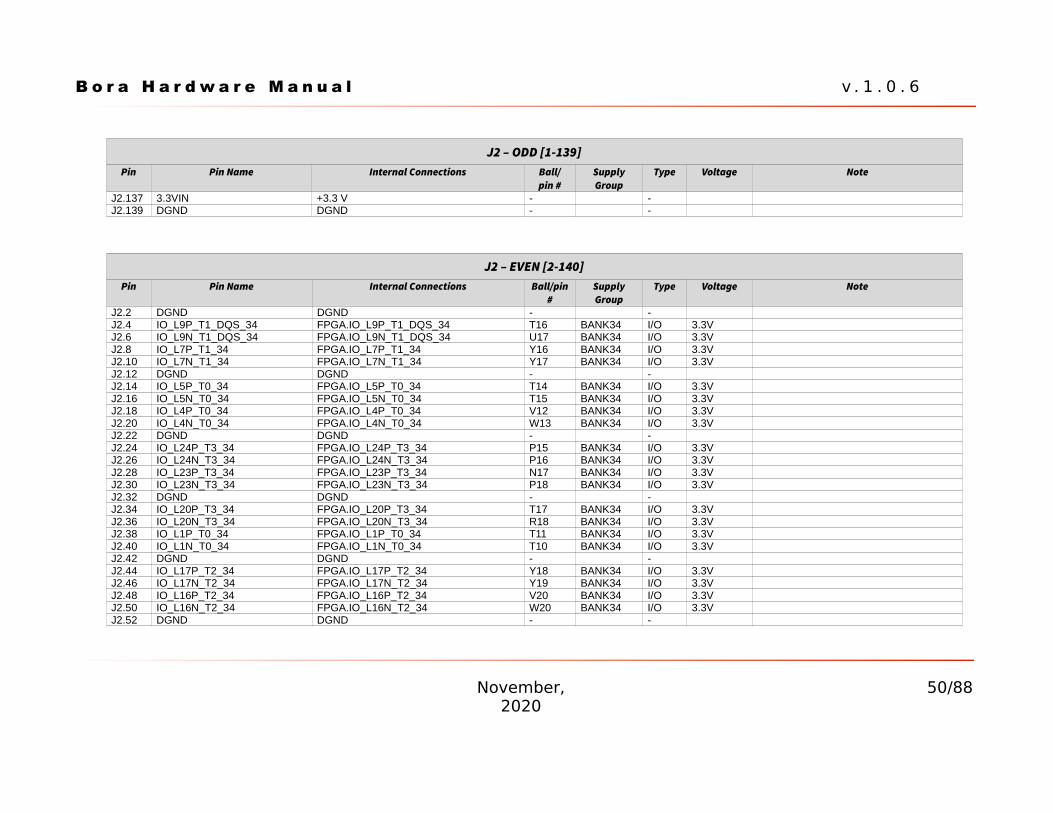
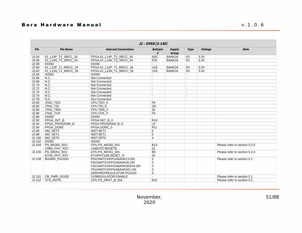
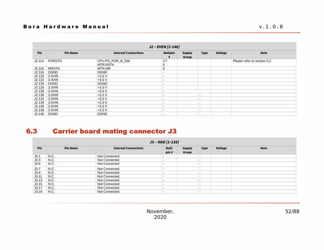
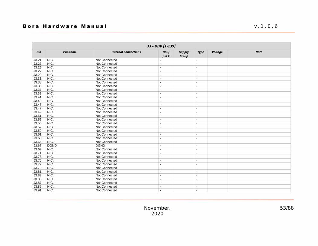
6 Pinout tableThis chapter contains the pinout description of the BORA module, grouped in six tables (two – odd and even pins – for each connector) that report the pin mapping of the three 140-pin BORA connectors.Each row in the pinout tables contains the following information:
Pin Reference to the connector pin
Pin Name Pin (signal) name on the BORA connectors
Internal Connections
Connections to the BORA components:CPU.<x> : pin connected to CPU (PS, processing system) pad named <x>FPGA.<x>: pin connected to FPGA (PL, programmable logic)pad named <x>CAN.<x> : pin connected to the CAN transceiverPMIC.<x> : pin connected to the Power Manager ICLAN.<x> : pin connected to the LAN PHYUSB.<x> : pin connected to the USB transceiverSV.<x>: pin connected to voltage supervisorMTR: pin connected to voltage monitors
Ball/pin # Component ball/pin number connected to signal
Supply Group Power Supply Group
Type Pin type: I = Input, O = Output, D= Differential, Z = High impedance, S = Supply voltage, G = Ground, A = Analog signal
Voltage I/O voltage
November, 202041/88
B o r a H a r d w a r e M a n u a l v . 1 . 0 . 6
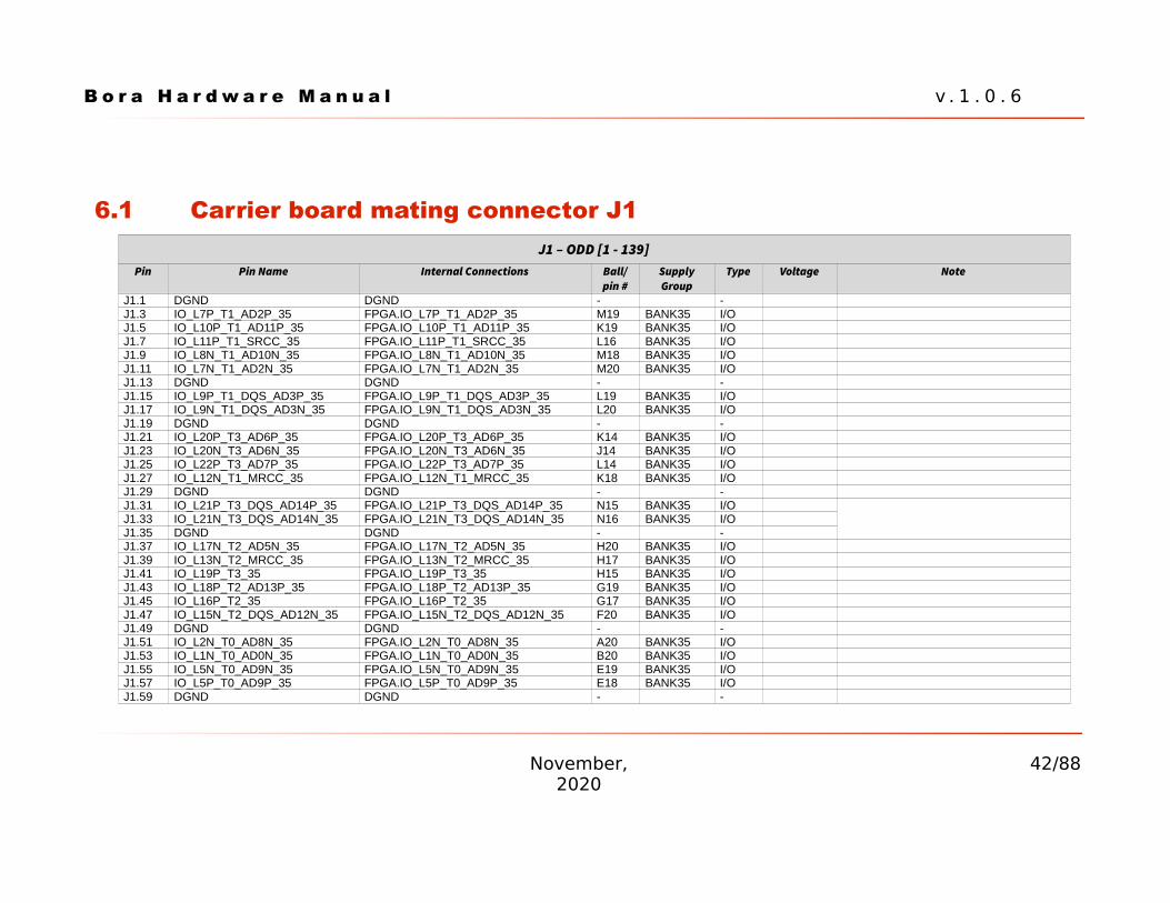
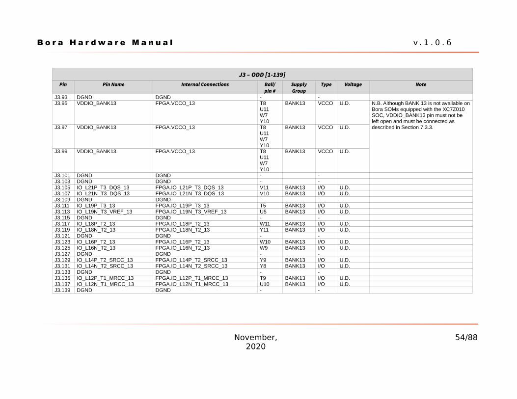
6.1 Carrier board mating connector J1J1 – ODD [1 - 139]
Pin Pin Name Internal Connections Ball/pin #
SupplyGroup
Type Voltage Note
J1.1 DGND DGND - -J1.3 IO_L7P_T1_AD2P_35 FPGA.IO_L7P_T1_AD2P_35 M19 BANK35 I/OJ1.5 IO_L10P_T1_AD11P_35 FPGA.IO_L10P_T1_AD11P_35 K19 BANK35 I/OJ1.7 IO_L11P_T1_SRCC_35 FPGA.IO_L11P_T1_SRCC_35 L16 BANK35 I/OJ1.9 IO_L8N_T1_AD10N_35 FPGA.IO_L8N_T1_AD10N_35 M18 BANK35 I/OJ1.11 IO_L7N_T1_AD2N_35 FPGA.IO_L7N_T1_AD2N_35 M20 BANK35 I/OJ1.13 DGND DGND - -J1.15 IO_L9P_T1_DQS_AD3P_35 FPGA.IO_L9P_T1_DQS_AD3P_35 L19 BANK35 I/OJ1.17 IO_L9N_T1_DQS_AD3N_35 FPGA.IO_L9N_T1_DQS_AD3N_35 L20 BANK35 I/OJ1.19 DGND DGND - -J1.21 IO_L20P_T3_AD6P_35 FPGA.IO_L20P_T3_AD6P_35 K14 BANK35 I/OJ1.23 IO_L20N_T3_AD6N_35 FPGA.IO_L20N_T3_AD6N_35 J14 BANK35 I/OJ1.25 IO_L22P_T3_AD7P_35 FPGA.IO_L22P_T3_AD7P_35 L14 BANK35 I/OJ1.27 IO_L12N_T1_MRCC_35 FPGA.IO_L12N_T1_MRCC_35 K18 BANK35 I/OJ1.29 DGND DGND - -J1.31 IO_L21P_T3_DQS_AD14P_35 FPGA.IO_L21P_T3_DQS_AD14P_35 N15 BANK35 I/OJ1.33 IO_L21N_T3_DQS_AD14N_35 FPGA.IO_L21N_T3_DQS_AD14N_35 N16 BANK35 I/OJ1.35 DGND DGND - -J1.37 IO_L17N_T2_AD5N_35 FPGA.IO_L17N_T2_AD5N_35 H20 BANK35 I/OJ1.39 IO_L13N_T2_MRCC_35 FPGA.IO_L13N_T2_MRCC_35 H17 BANK35 I/OJ1.41 IO_L19P_T3_35 FPGA.IO_L19P_T3_35 H15 BANK35 I/OJ1.43 IO_L18P_T2_AD13P_35 FPGA.IO_L18P_T2_AD13P_35 G19 BANK35 I/OJ1.45 IO_L16P_T2_35 FPGA.IO_L16P_T2_35 G17 BANK35 I/OJ1.47 IO_L15N_T2_DQS_AD12N_35 FPGA.IO_L15N_T2_DQS_AD12N_35 F20 BANK35 I/OJ1.49 DGND DGND - -J1.51 IO_L2N_T0_AD8N_35 FPGA.IO_L2N_T0_AD8N_35 A20 BANK35 I/OJ1.53 IO_L1N_T0_AD0N_35 FPGA.IO_L1N_T0_AD0N_35 B20 BANK35 I/OJ1.55 IO_L5N_T0_AD9N_35 FPGA.IO_L5N_T0_AD9N_35 E19 BANK35 I/OJ1.57 IO_L5P_T0_AD9P_35 FPGA.IO_L5P_T0_AD9P_35 E18 BANK35 I/OJ1.59 DGND DGND - -
November,2020
42/88
B o r a H a r d w a r e M a n u a l v . 1 . 0 . 6
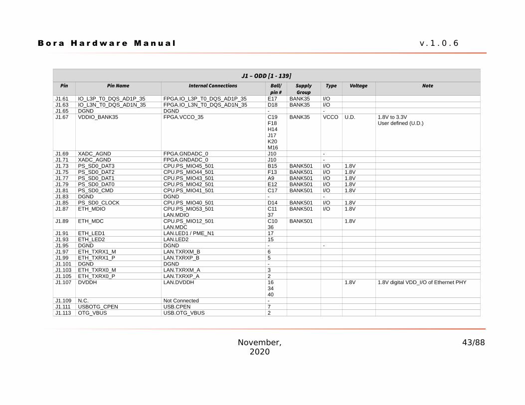
J1 – ODD [1 - 139]Pin Pin Name Internal Connections Ball/
pin #SupplyGroup
Type Voltage Note
J1.61 IO_L3P_T0_DQS_AD1P_35 FPGA.IO_L3P_T0_DQS_AD1P_35 E17 BANK35 I/OJ1.63 IO_L3N_T0_DQS_AD1N_35 FPGA.IO_L3N_T0_DQS_AD1N_35 D18 BANK35 I/OJ1.65 DGND DGND - -J1.67 VDDIO_BANK35 FPGA.VCCO_35 C19
F18H14J17K20M16
BANK35 VCCO U.D. 1.8V to 3.3VUser defined (U.D.)
J1.69 XADC_AGND FPGA.GNDADC_0 J10 -J1.71 XADC_AGND FPGA.GNDADC_0 J10 -J1.73 PS_SD0_DAT3 CPU.PS_MIO45_501 B15 BANK501 I/O 1.8VJ1.75 PS_SD0_DAT2 CPU.PS_MIO44_501 F13 BANK501 I/O 1.8VJ1.77 PS_SD0_DAT1 CPU.PS_MIO43_501 A9 BANK501 I/O 1.8VJ1.79 PS_SD0_DAT0 CPU.PS_MIO42_501 E12 BANK501 I/O 1.8VJ1.81 PS_SD0_CMD CPU.PS_MIO41_501 C17 BANK501 I/O 1.8VJ1.83 DGND DGND - -J1.85 PS_SD0_CLOCK CPU.PS_MIO40_501 D14 BANK501 I/O 1.8VJ1.87 ETH_MDIO CPU.PS_MIO53_501
LAN.MDIOC1137
BANK501 I/O 1.8V
J1.89 ETH_MDC CPU.PS_MIO12_501LAN.MDC
C1036
BANK501 1.8V
J1.91 ETH_LED1 LAN.LED1 / PME_N1 17J1.93 ETH_LED2 LAN.LED2 15J1.95 DGND DGND - -J1.97 ETH_TXRX1_M LAN.TXRXM_B 6J1.99 ETH_TXRX1_P LAN.TXRXP_B 5J1.101 DGND DGND -J1.103 ETH_TXRX0_M LAN.TXRXM_A 3J1.105 ETH_TXRX0_P LAN.TXRXP_A 2J1.107 DVDDH LAN.DVDDH 16
3440
1.8V 1.8V digital VDD_I/O of Ethernet PHY
J1.109 N.C. Not Connected -J1.111 USBOTG_CPEN USB.CPEN 7J1.113 OTG_VBUS USB.OTG_VBUS 2
November,2020
43/88
B o r a H a r d w a r e M a n u a l v . 1 . 0 . 6
J1 – ODD [1 - 139]Pin Pin Name Internal Connections Ball/
pin #SupplyGroup
Type Voltage Note
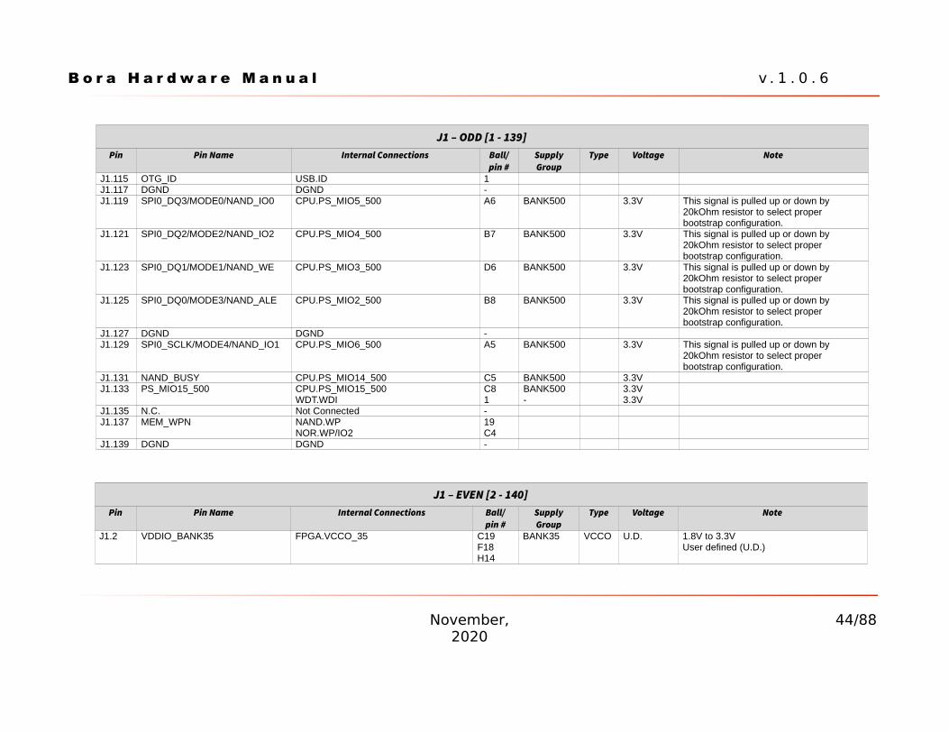
J1.115 OTG_ID USB.ID 1J1.117 DGND DGND -J1.119 SPI0_DQ3/MODE0/NAND_IO0 CPU.PS_MIO5_500 A6 BANK500 3.3V This signal is pulled up or down by
20kOhm resistor to select proper bootstrap configuration.
J1.121 SPI0_DQ2/MODE2/NAND_IO2 CPU.PS_MIO4_500 B7 BANK500 3.3V This signal is pulled up or down by 20kOhm resistor to select proper bootstrap configuration.
J1.123 SPI0_DQ1/MODE1/NAND_WE CPU.PS_MIO3_500 D6 BANK500 3.3V This signal is pulled up or down by 20kOhm resistor to select proper bootstrap configuration.
J1.125 SPI0_DQ0/MODE3/NAND_ALE CPU.PS_MIO2_500 B8 BANK500 3.3V This signal is pulled up or down by 20kOhm resistor to select proper bootstrap configuration.
J1.127 DGND DGND -J1.129 SPI0_SCLK/MODE4/NAND_IO1 CPU.PS_MIO6_500 A5 BANK500 3.3V This signal is pulled up or down by
20kOhm resistor to select proper bootstrap configuration.
J1.131 NAND_BUSY CPU.PS_MIO14_500 C5 BANK500 3.3VJ1.133 PS_MIO15_500 CPU.PS_MIO15_500
WDT.WDIC81
BANK500-
3.3V3.3V
J1.135 N.C. Not Connected -J1.137 MEM_WPN NAND.WP
NOR.WP/IO219C4
J1.139 DGND DGND -
J1 – EVEN [2 - 140]Pin Pin Name Internal Connections Ball/
pin #SupplyGroup
Type Voltage Note
J1.2 VDDIO_BANK35 FPGA.VCCO_35 C19F18H14
BANK35 VCCO U.D. 1.8V to 3.3VUser defined (U.D.)
November,2020
44/88
B o r a H a r d w a r e M a n u a l v . 1 . 0 . 6
J1 – EVEN [2 - 140]Pin Pin Name Internal Connections Ball/
pin #SupplyGroup
Type Voltage Note
J17K20M16
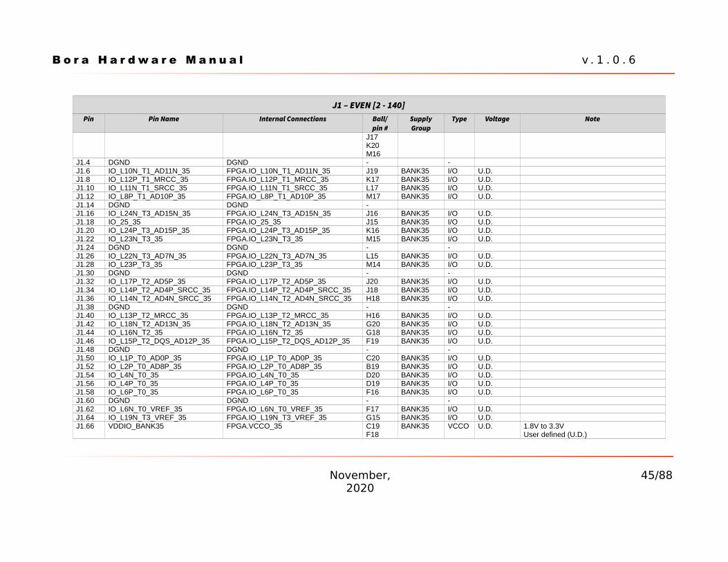
J1.4 DGND DGND - -J1.6 IO_L10N_T1_AD11N_35 FPGA.IO_L10N_T1_AD11N_35 J19 BANK35 I/O U.D.J1.8 IO_L12P_T1_MRCC_35 FPGA.IO_L12P_T1_MRCC_35 K17 BANK35 I/O U.D.J1.10 IO_L11N_T1_SRCC_35 FPGA.IO_L11N_T1_SRCC_35 L17 BANK35 I/O U.D.J1.12 IO_L8P_T1_AD10P_35 FPGA.IO_L8P_T1_AD10P_35 M17 BANK35 I/O U.D.J1.14 DGND DGND -J1.16 IO_L24N_T3_AD15N_35 FPGA.IO_L24N_T3_AD15N_35 J16 BANK35 I/O U.D.J1.18 IO_25_35 FPGA.IO_25_35 J15 BANK35 I/O U.D.J1.20 IO_L24P_T3_AD15P_35 FPGA.IO_L24P_T3_AD15P_35 K16 BANK35 I/O U.D.J1.22 IO_L23N_T3_35 FPGA.IO_L23N_T3_35 M15 BANK35 I/O U.D.J1.24 DGND DGND - -J1.26 IO_L22N_T3_AD7N_35 FPGA.IO_L22N_T3_AD7N_35 L15 BANK35 I/O U.D.J1.28 IO_L23P_T3_35 FPGA.IO_L23P_T3_35 M14 BANK35 I/O U.D.J1.30 DGND DGND - -J1.32 IO_L17P_T2_AD5P_35 FPGA.IO_L17P_T2_AD5P_35 J20 BANK35 I/O U.D.J1.34 IO_L14P_T2_AD4P_SRCC_35 FPGA.IO_L14P_T2_AD4P_SRCC_35 J18 BANK35 I/O U.D.J1.36 IO_L14N_T2_AD4N_SRCC_35 FPGA.IO_L14N_T2_AD4N_SRCC_35 H18 BANK35 I/O U.D.J1.38 DGND DGND - -J1.40 IO_L13P_T2_MRCC_35 FPGA.IO_L13P_T2_MRCC_35 H16 BANK35 I/O U.D.J1.42 IO_L18N_T2_AD13N_35 FPGA.IO_L18N_T2_AD13N_35 G20 BANK35 I/O U.D.J1.44 IO_L16N_T2_35 FPGA.IO_L16N_T2_35 G18 BANK35 I/O U.D.J1.46 IO_L15P_T2_DQS_AD12P_35 FPGA.IO_L15P_T2_DQS_AD12P_35 F19 BANK35 I/O U.D.J1.48 DGND DGND - -J1.50 IO_L1P_T0_AD0P_35 FPGA.IO_L1P_T0_AD0P_35 C20 BANK35 I/O U.D.J1.52 IO_L2P_T0_AD8P_35 FPGA.IO_L2P_T0_AD8P_35 B19 BANK35 I/O U.D.J1.54 IO_L4N_T0_35 FPGA.IO_L4N_T0_35 D20 BANK35 I/O U.D.J1.56 IO_L4P_T0_35 FPGA.IO_L4P_T0_35 D19 BANK35 I/O U.D.J1.58 IO_L6P_T0_35 FPGA.IO_L6P_T0_35 F16 BANK35 I/O U.D.J1.60 DGND DGND - -J1.62 IO_L6N_T0_VREF_35 FPGA.IO_L6N_T0_VREF_35 F17 BANK35 I/O U.D.J1.64 IO_L19N_T3_VREF_35 FPGA.IO_L19N_T3_VREF_35 G15 BANK35 I/O U.D.J1.66 VDDIO_BANK35 FPGA.VCCO_35 C19
F18BANK35 VCCO U.D. 1.8V to 3.3V
User defined (U.D.)
November,2020
45/88
B o r a H a r d w a r e M a n u a l v . 1 . 0 . 6
J1 – EVEN [2 - 140]Pin Pin Name Internal Connections Ball/
pin #SupplyGroup
Type Voltage Note
H14J17K20M16
J1.68 VDDIO_BANK35 FPGA.VCCO_35 C19F18H14J17K20M16
BANK35 VCCO U.D. 1.8V to 3.3VUser defined (U.D.)
J1.70 XADC_AGND FPGA.GNDADC_0 J10J1.72 XADC_AGND FPGA.GNDADC_0 J10J1.74 IO_0_35 FPGA.IO_0_35 G14 BANK35 I/O U.D.J1.76 N.C. Not Connected - BANK501 I/O 1.8VJ1.78 N.C. Not Connected - BANK501 I/O 1.8VJ1.80 PS_UART1_RX CPU.PS_MIO49_501 C12 BANK501 I/O 1.8VJ1.82 PS_UART1_TX CPU.PS_MIO48_501 B12 BANK501 I/O 1.8VJ1.84 PS_I2C0_DAT CPU.PS_MIO47_501 B14 BANK501 I/O 1.8VJ1.86 DGND DGND - -J1.88 PS_I2C0_CK CPU.PS_MIO46_501 D16 BANK501 I/O 1.8VJ1.90 ETH_INTN LAN.INT_N / PME_N2 38J1.92 DGND DGND - -J1.94 ETH_TXRX3_M LAN.TXRXM_D 11J1.96 ETH_TXRX3_P LAN.TXRXP_D 10J1.98 DGND DGND -J1.100 ETH_TXRX2_M LAN.TXRXM_C 8J1.102 ETH_TXRX2_P LAN.TXRXP_C 7J1.104 DGND DGND - -J1.106 CLK125_NDO LAN.CLK125_NDO 41J1.108 N.C. Not Connected -J1.110 N.C. Not Connected -J1.112 DGND DGND -J1.114 USBP1 USB.DP 6J1.116 USBM1 USB.DM 5J1.118 DGND DGND - -J1.120 SPI0_CS0N CPU.PS_MIO1_500 A7 BANK500 3.3V
November,2020
46/88
B o r a H a r d w a r e M a n u a l v . 1 . 0 . 6
J1 – EVEN [2 - 140]Pin Pin Name Internal Connections Ball/
pin #SupplyGroup
Type Voltage Note
NOR.CS# C2J1.122 NAND_CS0/SPI0_CS1 CPU.PS_MIO0_500
NAND.CE#E69
BANK500 3.3V
J1.124 NAND_IO3 CPU.PS_MIO13_500NAND.IO3
E832
BANK500 I/O 3.3V
J1.126 NAND_IO4 CPU.PS_MIO9_500NAND.IO4
B541
BANK500 I/O 3.3V
J1.128 NAND_IO5 CPU.PS_MIO10_500NAND.IO5
E942
BANK500 I/O 3.3V
J1.130 DGND DGND - -J1.132 NAND_IO6 CPU.PS_MIO11_500
NAND.IO6C643
BANK500 I/O 3.3V
J1.134 NAND_IO7 CPU.PS_MIO12_500NAND.IO7
D944
BANK500 I/O 3.3V
J1.136 NAND_RD_B/VCFG1 CPU.PS_MIO8_500NAND.RE#
D58
BANK500 3.3V This signal is pulled up or down by 20kOhm resistor to select proper bootstrap configuration.
J1.138 NAND_CLE/VCFG0 CPU.PS_MIO7_500NAND.CLE#
D816
BANK500 3.3V This signal is pulled up or down by 20kOhm resistor to select proper bootstrap configuration.
J1.140 DGND DGND -
6.2 Carrier board mating connector J2J2 – ODD [1-139]
Pin Pin Name Internal Connections Ball/pin #
SupplyGroup
Type Voltage Note
J2.1 DGND DGND - -J2.3 DGND DGND - -J2.5 IO_L8P_T1_34 FPGA.IO_L8P_T1_34 W14 BANK34 I/O 3.3VJ2.7 IO_L8N_T1_34 FPGA.IO_L8N_T1_34 Y14 BANK34 I/O 3.3V
November,2020
47/88
B o r a H a r d w a r e M a n u a l v . 1 . 0 . 6
J2 – ODD [1-139]Pin Pin Name Internal Connections Ball/
pin #SupplyGroup
Type Voltage Note
J2.9 IO_L6P_T0_34 CAN.DFPGA.IO_L6P_T0_34
1P14 BANK34
I/O3.3V
J2.11 IO_L6N_T0_VREF_34 FPGA.IO_L6N_T0_VREF_34 R14 BANK34 I/O 3.3VJ2.13 DGND DGND - -J2.15 IO_L3P_T0_DQS_PUDC_B_34 FPGA.IO_L3P_T0_DQS_PUDC_B_34 U13 BANK34 I/O 3.3V Internally connected to 3V3 via 10K
resistor J2.17 IO_L3N_T0_DQS_34 FPGA.IO_L3N_T0_DQS_34 V13 BANK34 I/O 3.3VJ2.19 IO_L2P_T0_34 FPGA.IO_L2P_T0_34 T12 BANK34 I/O 3.3VJ2.21 IO_L2N_T0_34 FPGA.IO_L2N_T0_34 U12 BANK34 I/O 3.3VJ2.23 DGND DGND - -J2.25 IO_L22P_T3_34 FPGA.IO_L22P_T3_34 W18 BANK34 I/O 3.3VJ2.27 IO_L22N_T3_34 FPGA.IO_L22N_T3_34 W19 BANK34 I/O 3.3VJ2.29 IO_L21P_T3_DQS_34 FPGA.IO_L21P_T3_DQS_34 V17 BANK34 I/O 3.3VJ2.31 IO_L21N_T3_DQS_34 FPGA.IO_L21N_T3_DQS_34 V18 BANK34 I/O 3.3VJ2.33 DGND DGND - -J2.35 IO_L19P_T3_34 CAN.R
FPGA.IO_L19P_T3_344R16 BANK34
I/O3.3V
J2.37 IO_L19N_T3_VREF_34 FPGA.IO_L19N_T3_VREF_34 R17 BANK34 I/O 3.3VJ2.39 IO_L18P_T2_34 FPGA.IO_L18P_T2_34 V16 BANK34 I/O 3.3VJ2.41 IO_L18N_T2_34 FPGA.IO_L18N_T2_34 W16 BANK34 I/O 3.3VJ2.43 DGND DGND - -J2.45 IO_L15P_T2_DQS_34 FPGA.IO_L15P_T2_DQS_34 T20 BANK34 I/O 3.3VJ2.47 IO_L15N_T2_DQS_34 FPGA.IO_L15N_T2_DQS_34 U20 BANK34 I/O 3.3VJ2.49 DGND DGND - -J2.51 IO_L13P_T1_MRCC_34 FPGA.IO_L13P_T1_MRCC_34 N18 BANK34 I/O 3.3VJ2.53 IO_L13N_T1_MRCC_34 FPGA.IO_L13N_T1_MRCC_34 P19 BANK34 I/O 3.3VJ2.55 DGND DGND - -J2.57 IO_L11P_T1_SRCC_34 FPGA.IO_L11P_T1_SRCC_34 U14 BANK34 I/O 3.3VJ2.59 IO_L11N_T1_SRCC_34 FPGA.IO_L11N_T1_SRCC_34 U15 BANK34 I/O 3.3VJ2.61 DGND DGND - -J2.63 IO_L10P_T1_34 FPGA.IO_L10P_T1_34 V15 BANK34 I/O 3.3VJ2.65 IO_L10N_T1_34 FPGA.IO_L10N_T1_34 W15 BANK34 I/O 3.3VJ2.67 IO_25_34 FPGA.IO_25_34 T19 BANK34 I/O 3.3VJ2.69 IO_0_34 FPGA.IO_0_34 R19 BANK34 I/O 3.3VJ2.71 DGND DGND - -J2.73 N.C. Not Connected - -
November,2020
48/88
B o r a H a r d w a r e M a n u a l v . 1 . 0 . 6
J2 – ODD [1-139]Pin Pin Name Internal Connections Ball/
pin #SupplyGroup
Type Voltage Note
J2.75 N.C. Not Connected - -J2.77 N.C. Not Connected - -J2.79 N.C. Not Connected - -J2.81 N.C. Not Connected - -J2.83 N.C. Not Connected - -J2.85 N.C. Not Connected - -J2.87 N.C. Not Connected - -J2.89 N.C. Not Connected - -J2.91 N.C. Not Connected - -J2.93 RTC_32KHZ RTC.32KHZ 1 -J2.95 RTC_RST RTC.RST# 4 -J2.97 XADC_VN_R FPGA.VN_0 L10 I/OJ2.99 XADC_VP_R FPGA.VP_0 K9 I/OJ2.101 N.C. Not Connected - -J2.103 CONN_SPI_RSTn NOR.RESET#/RFU A4 -J2.105 CAN_L CAN.L 6 I/OJ2.107 CAN_H CAN.H 7 I/OJ2.109 DGND DGND - -J2.111 RTC_INT/SQW RTC.RTC_INT/SQW 3 It can be left open if not used. When used,
a proper pull-up resistor is required on the carrier board. For further details, please refer to the Maxim Integrated DS3232 datasheet.
J2.113 RTC_VBAT RTC.VBAT 6J2.115 VBAT CPU.VCCBATT_0 F11 Please refer to Zynq-7000 Technical
Reference ManualJ2.117 DGND DGND - -J2.119 3.3VIN +3.3 V - -J2.121 3.3VIN +3.3 V - -J2.123 3.3VIN +3.3 V - -J2.125 DGND DGND - -J2.127 3.3VIN +3.3 V - -J2.129 3.3VIN +3.3 V - -J2.131 3.3VIN +3.3 V - -J2.133 3.3VIN +3.3 V - -J2.135 3.3VIN +3.3 V - -
November,2020
49/88
B o r a H a r d w a r e M a n u a l v . 1 . 0 . 6
J2 – ODD [1-139]Pin Pin Name Internal Connections Ball/
pin #SupplyGroup
Type Voltage Note
J2.137 3.3VIN +3.3 V - -J2.139 DGND DGND - -
J2 – EVEN [2-140]Pin Pin Name Internal Connections Ball/pin
#SupplyGroup
Type Voltage Note
J2.2 DGND DGND - -J2.4 IO_L9P_T1_DQS_34 FPGA.IO_L9P_T1_DQS_34 T16 BANK34 I/O 3.3VJ2.6 IO_L9N_T1_DQS_34 FPGA.IO_L9N_T1_DQS_34 U17 BANK34 I/O 3.3VJ2.8 IO_L7P_T1_34 FPGA.IO_L7P_T1_34 Y16 BANK34 I/O 3.3VJ2.10 IO_L7N_T1_34 FPGA.IO_L7N_T1_34 Y17 BANK34 I/O 3.3VJ2.12 DGND DGND - -J2.14 IO_L5P_T0_34 FPGA.IO_L5P_T0_34 T14 BANK34 I/O 3.3VJ2.16 IO_L5N_T0_34 FPGA.IO_L5N_T0_34 T15 BANK34 I/O 3.3VJ2.18 IO_L4P_T0_34 FPGA.IO_L4P_T0_34 V12 BANK34 I/O 3.3VJ2.20 IO_L4N_T0_34 FPGA.IO_L4N_T0_34 W13 BANK34 I/O 3.3VJ2.22 DGND DGND - -J2.24 IO_L24P_T3_34 FPGA.IO_L24P_T3_34 P15 BANK34 I/O 3.3VJ2.26 IO_L24N_T3_34 FPGA.IO_L24N_T3_34 P16 BANK34 I/O 3.3VJ2.28 IO_L23P_T3_34 FPGA.IO_L23P_T3_34 N17 BANK34 I/O 3.3VJ2.30 IO_L23N_T3_34 FPGA.IO_L23N_T3_34 P18 BANK34 I/O 3.3VJ2.32 DGND DGND - -J2.34 IO_L20P_T3_34 FPGA.IO_L20P_T3_34 T17 BANK34 I/O 3.3VJ2.36 IO_L20N_T3_34 FPGA.IO_L20N_T3_34 R18 BANK34 I/O 3.3VJ2.38 IO_L1P_T0_34 FPGA.IO_L1P_T0_34 T11 BANK34 I/O 3.3VJ2.40 IO_L1N_T0_34 FPGA.IO_L1N_T0_34 T10 BANK34 I/O 3.3VJ2.42 DGND DGND - -J2.44 IO_L17P_T2_34 FPGA.IO_L17P_T2_34 Y18 BANK34 I/O 3.3VJ2.46 IO_L17N_T2_34 FPGA.IO_L17N_T2_34 Y19 BANK34 I/O 3.3VJ2.48 IO_L16P_T2_34 FPGA.IO_L16P_T2_34 V20 BANK34 I/O 3.3VJ2.50 IO_L16N_T2_34 FPGA.IO_L16N_T2_34 W20 BANK34 I/O 3.3VJ2.52 DGND DGND - -
November,2020
50/88
B o r a H a r d w a r e M a n u a l v . 1 . 0 . 6
J2 – EVEN [2-140]Pin Pin Name Internal Connections Ball/pin
#SupplyGroup
Type Voltage Note
J2.54 IO_L14P_T2_SRCC_34 FPGA.IO_L14P_T2_SRCC_34 N20 BANK34 I/O 3.3VJ2.56 IO_L14N_T2_SRCC_34 FPGA.IO_L14N_T2_SRCC_34 P20 BANK34 I/O 3.3VJ2.58 DGND DGND - -J2.60 IO_L12P_T1_MRCC_34 FPGA.IO_L12P_T1_MRCC_34 U18 BANK34 I/O 3.3VJ2.62 IO_L12N_T1_MRCC_34 FPGA.IO_L12N_T1_MRCC_34 U19 BANK34 I/O 3.3VJ2.64 DGND DGND - -J2.66 N.C. Not Connected - -J2.68 N.C. Not Connected - -J2.70 N.C. Not Connected - -J2.72 N.C. Not Connected - -J2.74 N.C. Not Connected - -J2.76 N.C. Not Connected - -J2.78 N.C. Not Connected - -J2.80 JTAG_TDO CPU.TDO_0 F6J2.82 JTAG_TDI CPU.TDI_0 G6J2.84 JTAG_TMS CPU.TMS_0 J6J2.86 JTAG_TCK CPU.TCK_0 F9J2.88 DGND DGND -J2.90 FPGA_INIT_B FPGA.INIT_B_0 R10J2.92 FPGA_PROGRAM_B FPGA.PROGRAM_B_0 L6J2.94 FPGA_DONE FPGA.DONE_0 R11J2.96 WD_SET2 WDT.SET2 6J2.98 WD_SET1 WDT.SET1 5J2.100 WD_SET0 WDT.SET0 4J2.102 DGND DGND -J2.104 PS_MIO50_501/
USB0_PHY_RSTCPU.PS_MIO50_501USBOTG.RESETB
B1322
Please refer to section 5.2.5
J2.106 PS_MIO51_501/ETH0_PHY_RST
CPU.PS_MIO51_501ETHPHY1GB.RESET_N
B942
Please refer to section 5.2.4
J2.108 BOARD_PGOOD PSUSWITCHFPGABANK13.ONPSUSWITCHFPGABANK35.ONPSUSWITCHFPGABANK500/34.ONPSUSWITCHFPGABANK501.ONDDRVREFREGULATOR.PGOOD
33339
Please refer to section 5.1
J2.110 CB_PWR_GOOD 1V0REGULATOR.ENABLE - Please refer to section 5.1J2.112 SYS_RSTN CPU.PS_SRST_B_501 B10 Please refer to section 5.2
November,2020
51/88
B o r a H a r d w a r e M a n u a l v . 1 . 0 . 6
J2 – EVEN [2-140]Pin Pin Name Internal Connections Ball/pin
#SupplyGroup
Type Voltage Note
J2.114 PORSTN CPU.PS_POR_B_500MTR.RST#
C75
Please refer to section 5.2
J2.116 MRSTN MTR.MR 6J2.118 DGND DGND -J2.120 3.3VIN +3.3 V -J2.122 3.3VIN +3.3 V -J2.124 DGND DGND -J2.126 3.3VIN +3.3 V -J2.128 3.3VIN +3.3 V -J2.130 3.3VIN +3.3 V - -J2.132 3.3VIN +3.3 V - -J2.134 3.3VIN +3.3 V - -J2.136 3.3VIN +3.3 V - -J2.138 3.3VIN +3.3 V - -J2.140 DGND DGND - -
6.3 Carrier board mating connector J3J3 – ODD [1-139]
Pin Pin Name Internal Connections Ball/pin #
SupplyGroup
Type Voltage Note
J3.1 N.C. Not Connected - -J3.3 N.C. Not Connected - -J3.5 N.C. Not Connected - -
J3.7 N.C. Not Connected - -J3.9 N.C. Not Connected - -J3.11 N.C. Not Connected - -J3.13 N.C. Not Connected - -J3.15 N.C. Not Connected - -J3.17 N.C. Not Connected - -J3.19 N.C. Not Connected - -
November,2020
52/88
B o r a H a r d w a r e M a n u a l v . 1 . 0 . 6
J3 – ODD [1-139]Pin Pin Name Internal Connections Ball/
pin #SupplyGroup
Type Voltage Note
J3.21 N.C. Not Connected - -J3.23 N.C. Not Connected - -J3.25 N.C. Not Connected - -J3.27 N.C. Not Connected - -J3.29 N.C. Not Connected - -J3.31 N.C. Not Connected - -J3.33 N.C. Not Connected - -J3.35 N.C. Not Connected - -J3.37 N.C. Not Connected - -J3.39 N.C. Not Connected - -J3.41 N.C. Not Connected - -J3.43 N.C. Not Connected - -J3.45 N.C. Not Connected - -J3.47 N.C. Not Connected - -J3.49 N.C. Not Connected - -J3.51 N.C. Not Connected - -J3.53 N.C. Not Connected - -J3.55 N.C. Not Connected - -J3.57 N.C. Not Connected - -J3.59 N.C. Not Connected - -J3.61 N.C. Not Connected - -J3.63 N.C. Not Connected - -J3.65 N.C. Not Connected - -J3.67 DGND DGND - -J3.69 N.C. Not Connected - -J3.71 N.C. Not Connected - -J3.73 N.C. Not Connected - -J3.75 N.C. Not Connected - -J3.77 N.C. Not Connected - -J3.79 N.C. Not Connected - -J3.81 N.C. Not Connected - -J3.83 N.C. Not Connected - -J3.85 N.C. Not Connected - -J3.87 N.C. Not Connected - -J3.89 N.C. Not Connected - -J3.91 N.C. Not Connected - -
November,2020
53/88
B o r a H a r d w a r e M a n u a l v . 1 . 0 . 6
J3 – ODD [1-139]Pin Pin Name Internal Connections Ball/
pin #SupplyGroup
Type Voltage Note
J3.93 DGND DGND - -J3.95 VDDIO_BANK13 FPGA.VCCO_13 T8
U11W7Y10
BANK13 VCCO U.D. N.B. Although BANK 13 is not available onBora SOMs equipped with the XC7Z010 SOC, VDDIO_BANK13 pin must not be left open and must be connected as described in Section 7.3.3.J3.97 VDDIO_BANK13 FPGA.VCCO_13 T8
U11W7Y10
BANK13 VCCO U.D.
J3.99 VDDIO_BANK13 FPGA.VCCO_13 T8U11W7Y10
BANK13 VCCO U.D.
J3.101 DGND DGND - -J3.103 DGND DGND - -J3.105 IO_L21P_T3_DQS_13 FPGA.IO_L21P_T3_DQS_13 V11 BANK13 I/O U.D.J3.107 IO_L21N_T3_DQS_13 FPGA.IO_L21N_T3_DQS_13 V10 BANK13 I/O U.D.J3.109 DGND DGND - -J3.111 IO_L19P_T3_13 FPGA.IO_L19P_T3_13 T5 BANK13 I/O U.D.J3.113 IO_L19N_T3_VREF_13 FPGA.IO_L19N_T3_VREF_13 U5 BANK13 I/O U.D.J3.115 DGND DGND - -J3.117 IO_L18P_T2_13 FPGA.IO_L18P_T2_13 W11 BANK13 I/O U.D.J3.119 IO_L18N_T2_13 FPGA.IO_L18N_T2_13 Y11 BANK13 I/O U.D.J3.121 DGND DGND - -J3.123 IO_L16P_T2_13 FPGA.IO_L16P_T2_13 W10 BANK13 I/O U.D.J3.125 IO_L16N_T2_13 FPGA.IO_L16N_T2_13 W9 BANK13 I/O U.D.J3.127 DGND DGND - -J3.129 IO_L14P_T2_SRCC_13 FPGA.IO_L14P_T2_SRCC_13 Y9 BANK13 I/O U.D.J3.131 IO_L14N_T2_SRCC_13 FPGA.IO_L14N_T2_SRCC_13 Y8 BANK13 I/O U.D.J3.133 DGND DGND - -J3.135 IO_L12P_T1_MRCC_13 FPGA.IO_L12P_T1_MRCC_13 T9 BANK13 I/O U.D.J3.137 IO_L12N_T1_MRCC_13 FPGA.IO_L12N_T1_MRCC_13 U10 BANK13 I/O U.D.J3.139 DGND DGND - -
November,2020
54/88
B o r a H a r d w a r e M a n u a l v . 1 . 0 . 6
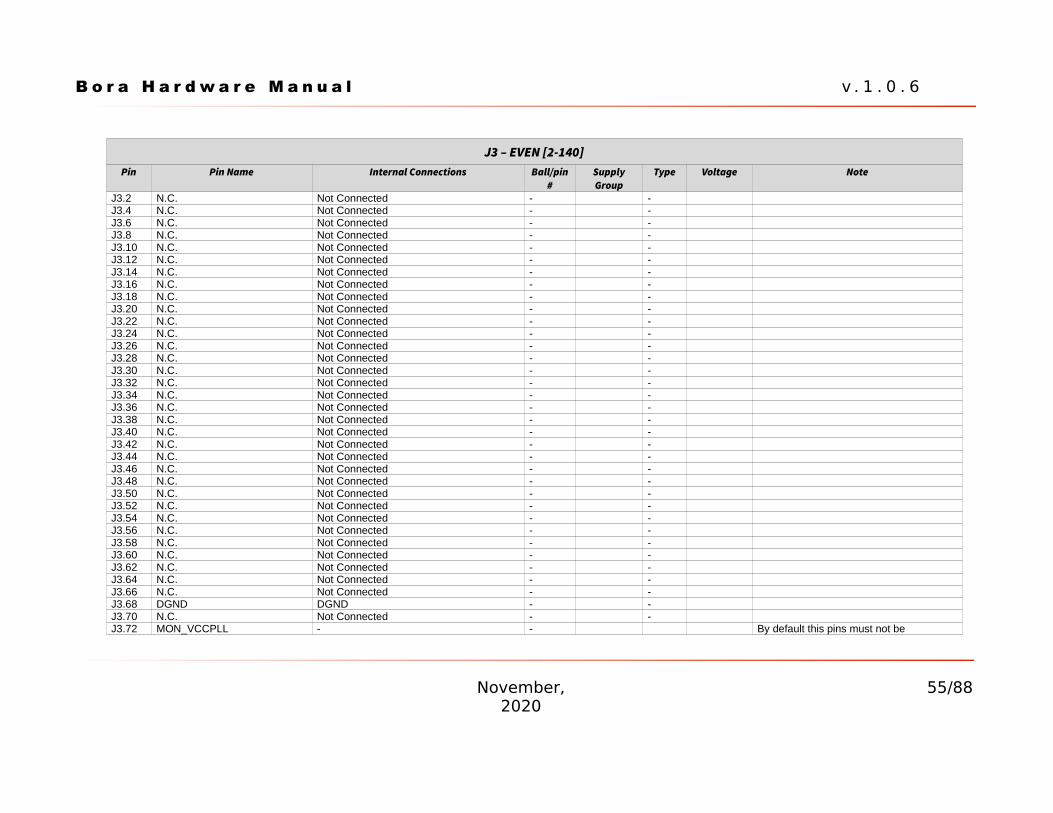
J3 – EVEN [2-140]Pin Pin Name Internal Connections Ball/pin
#SupplyGroup
Type Voltage Note
J3.2 N.C. Not Connected - -J3.4 N.C. Not Connected - -J3.6 N.C. Not Connected - -J3.8 N.C. Not Connected - -J3.10 N.C. Not Connected - -J3.12 N.C. Not Connected - -J3.14 N.C. Not Connected - -J3.16 N.C. Not Connected - -J3.18 N.C. Not Connected - -J3.20 N.C. Not Connected - -J3.22 N.C. Not Connected - -J3.24 N.C. Not Connected - -J3.26 N.C. Not Connected - -J3.28 N.C. Not Connected - -J3.30 N.C. Not Connected - -J3.32 N.C. Not Connected - -J3.34 N.C. Not Connected - -J3.36 N.C. Not Connected - -J3.38 N.C. Not Connected - -J3.40 N.C. Not Connected - -J3.42 N.C. Not Connected - -J3.44 N.C. Not Connected - -J3.46 N.C. Not Connected - -J3.48 N.C. Not Connected - -J3.50 N.C. Not Connected - -J3.52 N.C. Not Connected - -J3.54 N.C. Not Connected - -J3.56 N.C. Not Connected - -J3.58 N.C. Not Connected - -J3.60 N.C. Not Connected - -J3.62 N.C. Not Connected - -J3.64 N.C. Not Connected - -J3.66 N.C. Not Connected - -J3.68 DGND DGND - -J3.70 N.C. Not Connected - -J3.72 MON_VCCPLL - - By default this pins must not be
November,2020
55/88
B o r a H a r d w a r e M a n u a l v . 1 . 0 . 6
J3 – EVEN [2-140]Pin Pin Name Internal Connections Ball/pin
#SupplyGroup
Type Voltage Note
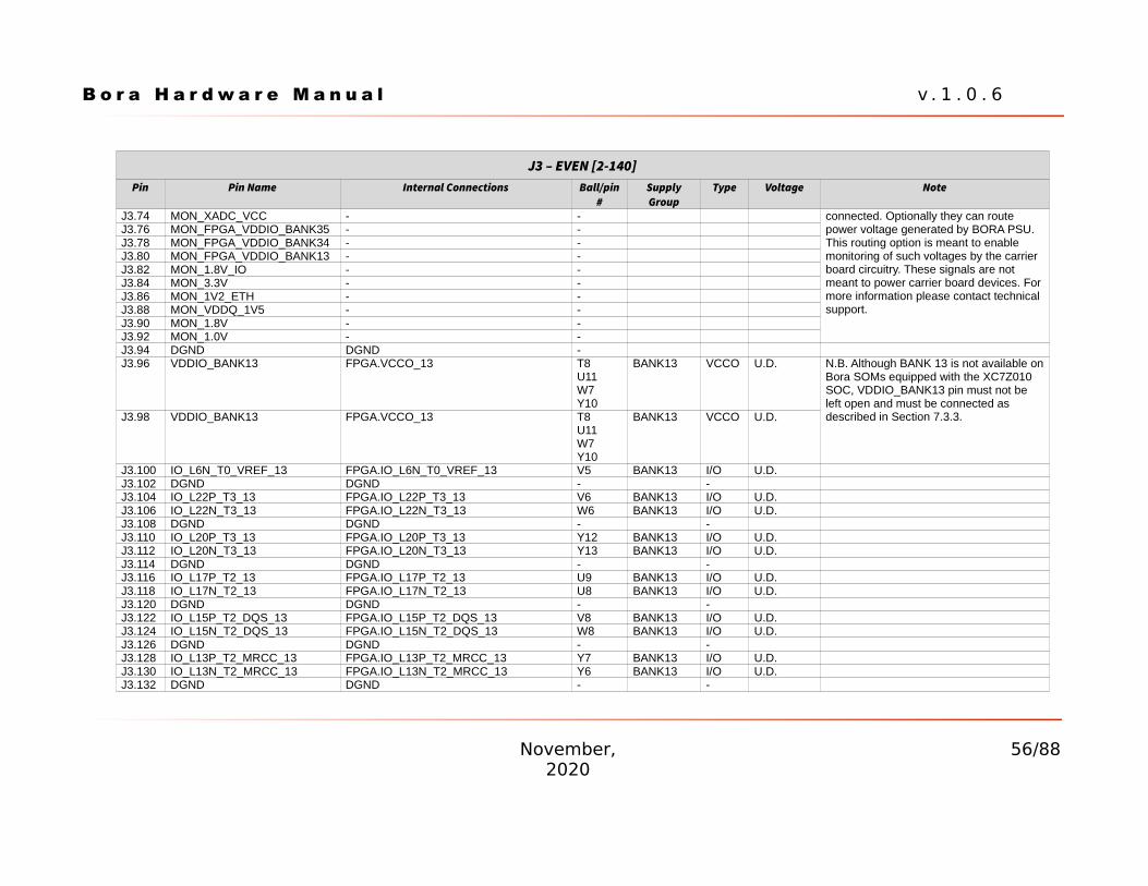
connected. Optionally they can route power voltage generated by BORA PSU.This routing option is meant to enable monitoring of such voltages by the carrier board circuitry. These signals are not meant to power carrier board devices. For more information please contact technical support.
J3.74 MON_XADC_VCC - -J3.76 MON_FPGA_VDDIO_BANK35 - -J3.78 MON_FPGA_VDDIO_BANK34 - -J3.80 MON_FPGA_VDDIO_BANK13 - -J3.82 MON_1.8V_IO - -J3.84 MON_3.3V - -J3.86 MON_1V2_ETH - -J3.88 MON_VDDQ_1V5 - -J3.90 MON_1.8V - -J3.92 MON_1.0V - -J3.94 DGND DGND -J3.96 VDDIO_BANK13 FPGA.VCCO_13 T8
U11W7Y10
BANK13 VCCO U.D. N.B. Although BANK 13 is not available onBora SOMs equipped with the XC7Z010 SOC, VDDIO_BANK13 pin must not be left open and must be connected as described in Section 7.3.3.J3.98 VDDIO_BANK13 FPGA.VCCO_13 T8
U11W7Y10
BANK13 VCCO U.D.
J3.100 IO_L6N_T0_VREF_13 FPGA.IO_L6N_T0_VREF_13 V5 BANK13 I/O U.D.J3.102 DGND DGND - -J3.104 IO_L22P_T3_13 FPGA.IO_L22P_T3_13 V6 BANK13 I/O U.D.J3.106 IO_L22N_T3_13 FPGA.IO_L22N_T3_13 W6 BANK13 I/O U.D.J3.108 DGND DGND - -J3.110 IO_L20P_T3_13 FPGA.IO_L20P_T3_13 Y12 BANK13 I/O U.D.J3.112 IO_L20N_T3_13 FPGA.IO_L20N_T3_13 Y13 BANK13 I/O U.D.J3.114 DGND DGND - -J3.116 IO_L17P_T2_13 FPGA.IO_L17P_T2_13 U9 BANK13 I/O U.D.J3.118 IO_L17N_T2_13 FPGA.IO_L17N_T2_13 U8 BANK13 I/O U.D.J3.120 DGND DGND - -J3.122 IO_L15P_T2_DQS_13 FPGA.IO_L15P_T2_DQS_13 V8 BANK13 I/O U.D.J3.124 IO_L15N_T2_DQS_13 FPGA.IO_L15N_T2_DQS_13 W8 BANK13 I/O U.D.J3.126 DGND DGND - -J3.128 IO_L13P_T2_MRCC_13 FPGA.IO_L13P_T2_MRCC_13 Y7 BANK13 I/O U.D.J3.130 IO_L13N_T2_MRCC_13 FPGA.IO_L13N_T2_MRCC_13 Y6 BANK13 I/O U.D.J3.132 DGND DGND - -
November,2020
56/88
B o r a H a r d w a r e M a n u a l v . 1 . 0 . 6
J3 – EVEN [2-140]Pin Pin Name Internal Connections Ball/pin
#SupplyGroup
Type Voltage Note
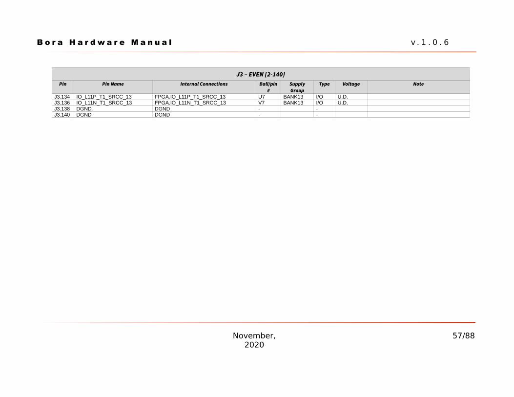
J3.134 IO_L11P_T1_SRCC_13 FPGA.IO_L11P_T1_SRCC_13 U7 BANK13 I/O U.D.J3.136 IO_L11N_T1_SRCC_13 FPGA.IO_L11N_T1_SRCC_13 V7 BANK13 I/O U.D.J3.138 DGND DGND - -J3.140 DGND DGND - -
November,2020
57/88
B o r a H a r d w a r e M a n u a l v . 1 . 0 . 6
7 Peripheral interfacesBORA modules implement a number of peripheral interfaces through the J1, J2 and J3 connectors. The following notes apply to those interfaces: Some interfaces/signals are available only with/without
certain configuration options of the BORA module. Each signal’s availability is noted in the “Notes” column on the table of each interface.
The peripherals described in the following sections represent the default configuration for the BORA SOM, which match with the features provided by the electronics implemented on the module. As an example, the Zynq device provides twoUSB 2.0 controllers, but the BORA SOM provides one USB OTG port, with transceiver connected to one of the controllers and signals routed to the module connectors. Therefore, only one USB port will be described in details.
The signals for each interface are described in the related tables. The following notes summarize the column headers for these tables: “Pin name” – The symbolic name of each signal
“Conn. Pin” – The pin number on the module connectors
“Function” – Signal description
“Notes” – This column summarizes configuration requirements and recommendations for each signal.
7.1 Notes on pin assignmentFor further information, please refer to section 5.7 “Multiplexing“. For detailed information on MIO and EMIO configuration, please refer to section 2.5.1 /“I/O Peripheral (IOP) Interface Routing”) of the Zynq-7000 Technical Reference Manual.
On the BORA SOM, the MIO module is configured for providing a standard set of peripherals (eg, Ethernet, USB, …); some pins of the EMIO are also used to implement some functions (eg: I2C,
November, 202058/88
B o r a H a r d w a r e M a n u a l v . 1 . 0 . 6
specific I/Os). Plese refer to the following sections for detailed information.
7.2 PS interfacesThe 54 pins of the MIO module are assigned as reported in the following table:
MIO pins FunctionMIO[0:14] Quad-SPI and NAND flash
MIO[15] EX_WDT_REARM (watchdog WDI)Optionally, it can act as SWDT reset out
MIO[16:27] Gigabit Ethernet
MIO[28:39] USB On-The-Go
MIO[40:45] SD/SDIO/MMC
MIO[46:47] I²C0
MIO[48:49] UART1
MIO[52] Ethernet Management Data Clock input
MIO[53] Ethernet Management Data Input/Output
7.2.1 Gigabit EthernetOn-board Ethernet PHY (Micrel KSZ9031RNX) provides interface signals required to implement the 10/100/1000 Mbps Ethernet port. The transceiver is connected to the Gigabit Ethernet Controller (GEM) through RGMII interface on MIO bank 1, pins PS_MIO[16:27]. For further details (eg: connection and selection of the magnetics), please refer to the Micrel KSZ9031RNX datasheet.
The following table describes the interface signals:
Pin name Conn.Pin
Function Notes
ETH_TXRX0_P J1.105 Media Dependent Interface[0], positive pin
ETH_TXRX0_M J1.103 Media Dependent Interface[0], negative pin
ETH_TXRX1_P J1.99 Media Dependent Interface[1], positive pin
November, 202059/88
B o r a H a r d w a r e M a n u a l v . 1 . 0 . 6
Pin name Conn.Pin
Function Notes
ETH_TXRX1_M J1.97 Media Dependent Interface[1], negative pin
ETH_TXRX2_P J1.102 Media Dependent Interface[2], positive pin
ETH_TXRX2_M J1.100 Media Dependent Interface[2], negative pin
ETH_TXRX3_P J1.96 Media Dependent Interface[3], positive pin
ETH_TXRX3_M J1.94 Media Dependent Interface[3], negative pin
ETH_MDIO J1.87 Management Data Input/Output
ETH_MDC J1.89 Management Data Clock input
ETH_INTn J1.90 Interrupt output
ETH_LED1 J1.91 Activity LED
ETH_LED2 J1.93 Link LED
DVDDH J1.107 1.8V digital VDD_I/O of Ethernet PHY
7.2.2 USBBORA provides one USB 2.0 (Full Speed, up to 480 Mbps) port with on-board PHY (SMSC USB3317) and support to the On-The-Go (OTG) specifications. The transceiver is connected to the USB1 controller (MIO bank 1, pins PS_MIO[28:39]).
The following table describes the interface signals:
Pin name Conn. Pin
Function Notes
USBP1 J1.114 D+ pin of the USB cable
USBM1 J1.116 D- pin of the USB cable
USBOTG_CPEN J1.111 External 5 volt supply enable.
This pin is used to enable the external Vbus power supply.
OTG_VBUS J1.113 VBUS pin of the USB
November, 202060/88
B o r a H a r d w a r e M a n u a l v . 1 . 0 . 6
Pin name Conn. Pin
Function Notes
cable
OTG_ID J1.115 ID pin of the USB cable For non-OTG applications this pin canbe floated. For an A-device ID is grounded. For a B-device ID is floated.
7.2.3 Quad-SPIQuad-SPI is used to access multi-bit serial flash memory devicesfor high throughput and low pin count applications. The controller operates in one of three modes: I/O mode, linear addressing mode, and legacy SPI mode.
The following table describes the interface signals:
Pin name Conn. Pin
Function Notes
SPI0_CS0 J1.120 Chip select 0 MIO bank 0, pin 1
SPI0_CS1 J1.122 Chip select 1 MIO bank 0, pin 0
SPI0_DQ0 J1.125 1-bit: Master Output2-bit: I/O04-bit: I/O0
MIO bank 0, pin 2
SPI0_DQ1 J1.123 1-bit: Master Input2-bit: I/O14-bit: I/O1
MIO bank 0, pin 3
SPI0_DQ2 J1.121 1-bit: Write protect2-bit: Write protect4-bit: I/O0
MIO bank 0, pin 4
SPI0_DQ3 J1.119 1-bit: Hold2-bit: Hold4-bit: I/O3
MIO bank 0, pin 5
SPI0_SCLK J1.129 Serial clock MIO bank 0, pin 6
7.2.4 Static memory controller (NAND)Static memory controller (SMC) signals are routed to the connectors to connect an external flash NAND memory chip.
November, 202061/88
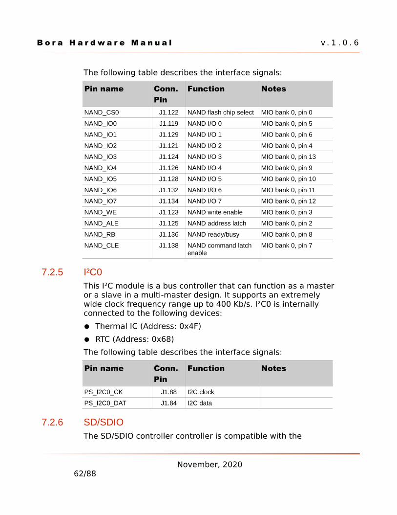
B o r a H a r d w a r e M a n u a l v . 1 . 0 . 6
The following table describes the interface signals:
Pin name Conn. Pin
Function Notes
NAND_CS0 J1.122 NAND flash chip select MIO bank 0, pin 0
NAND_IO0 J1.119 NAND I/O 0 MIO bank 0, pin 5
NAND_IO1 J1.129 NAND I/O 1 MIO bank 0, pin 6
NAND_IO2 J1.121 NAND I/O 2 MIO bank 0, pin 4
NAND_IO3 J1.124 NAND I/O 3 MIO bank 0, pin 13
NAND_IO4 J1.126 NAND I/O 4 MIO bank 0, pin 9
NAND_IO5 J1.128 NAND I/O 5 MIO bank 0, pin 10
NAND_IO6 J1.132 NAND I/O 6 MIO bank 0, pin 11
NAND_IO7 J1.134 NAND I/O 7 MIO bank 0, pin 12
NAND_WE J1.123 NAND write enable MIO bank 0, pin 3
NAND_ALE J1.125 NAND address latch MIO bank 0, pin 2
NAND_RB J1.136 NAND ready/busy MIO bank 0, pin 8
NAND_CLE J1.138 NAND command latch enable
MIO bank 0, pin 7
7.2.5 I²C0This I²C module is a bus controller that can function as a master or a slave in a multi-master design. It supports an extremely wide clock frequency range up to 400 Kb/s. I²C0 is internally connected to the following devices:
Thermal IC (Address: 0x4F)
RTC (Address: 0x68)
The following table describes the interface signals:
Pin name Conn. Pin
Function Notes
PS_I2C0_CK J1.88 I2C clock
PS_I2C0_DAT J1.84 I2C data
7.2.6 SD/SDIOThe SD/SDIO controller controller is compatible with the
November, 202062/88
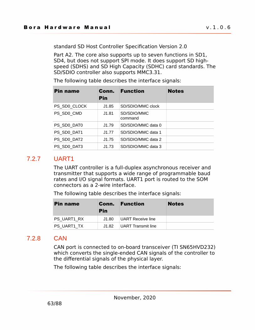
B o r a H a r d w a r e M a n u a l v . 1 . 0 . 6
standard SD Host Controller Specification Version 2.0
Part A2. The core also supports up to seven functions in SD1, SD4, but does not support SPI mode. It does support SD high-speed (SDHS) and SD High Capacity (SDHC) card standards. TheSD/SDIO controller also supports MMC3.31.
The following table describes the interface signals:
Pin name Conn. Pin
Function Notes
PS_SD0_CLOCK J1.85 SD/SDIO/MMC clock
PS_SD0_CMD J1.81 SD/SDIO/MMC command
PS_SD0_DAT0 J1.79 SD/SDIO/MMC data 0
PS_SD0_DAT1 J1.77 SD/SDIO/MMC data 1
PS_SD0_DAT2 J1.75 SD/SDIO/MMC data 2
PS_SD0_DAT3 J1.73 SD/SDIO/MMC data 3
7.2.7 UART1The UART controller is a full-duplex asynchronous receiver and transmitter that supports a wide range of programmable baud rates and I/O signal formats. UART1 port is routed to the SOM connectors as a 2-wire interface.
The following table describes the interface signals:
Pin name Conn. Pin
Function Notes
PS_UART1_RX J1.80 UART Receive line
PS_UART1_TX J1.82 UART Transmit line
7.2.8 CANCAN port is connected to on-board transceiver (TI SN65HVD232)which converts the single-ended CAN signals of the controller to the differential signals of the physical layer.
The following table describes the interface signals:
November, 202063/88
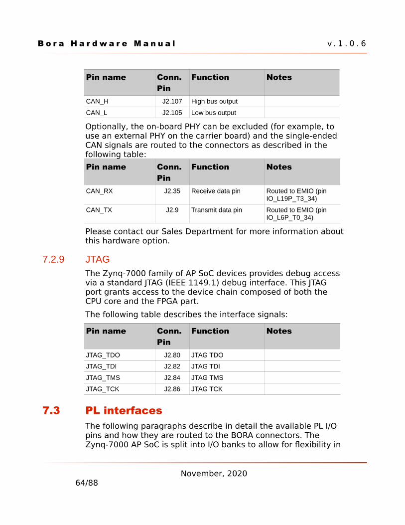
B o r a H a r d w a r e M a n u a l v . 1 . 0 . 6
Pin name Conn. Pin
Function Notes
CAN_H J2.107 High bus output
CAN_L J2.105 Low bus output
Optionally, the on-board PHY can be excluded (for example, to use an external PHY on the carrier board) and the single-ended CAN signals are routed to the connectors as described in the following table:
Pin name Conn. Pin
Function Notes
CAN_RX J2.35 Receive data pin Routed to EMIO (pin IO_L19P_T3_34)
CAN_TX J2.9 Transmit data pin Routed to EMIO (pin IO_L6P_T0_34)
Please contact our Sales Department for more information aboutthis hardware option.
7.2.9 JTAGThe Zynq-7000 family of AP SoC devices provides debug access via a standard JTAG (IEEE 1149.1) debug interface. This JTAG port grants access to the device chain composed of both the CPU core and the FPGA part.
The following table describes the interface signals:
Pin name Conn. Pin
Function Notes
JTAG_TDO J2.80 JTAG TDO
JTAG_TDI J2.82 JTAG TDI
JTAG_TMS J2.84 JTAG TMS
JTAG_TCK J2.86 JTAG TCK
7.3 PL interfacesThe following paragraphs describe in detail the available PL I/O pins and how they are routed to the BORA connectors. The Zynq-7000 AP SoC is split into I/O banks to allow for flexibility in
November, 202064/88
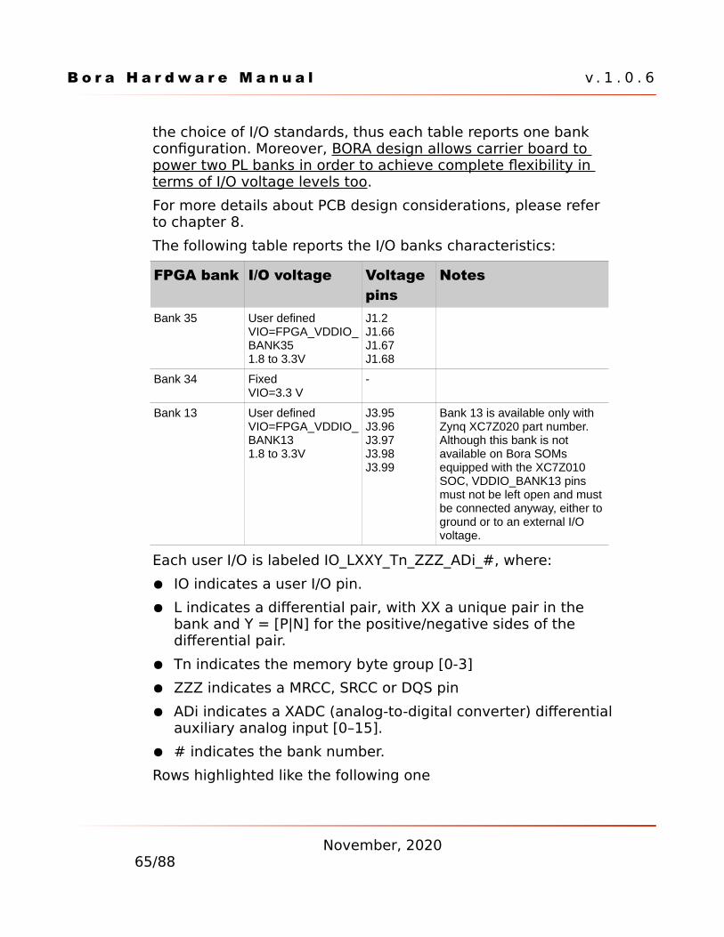
B o r a H a r d w a r e M a n u a l v . 1 . 0 . 6
the choice of I/O standards, thus each table reports one bank configuration. Moreover, BORA design allows carrier board to power two PL banks in order to achieve complete flexibility in terms of I/O voltage levels too.
For more details about PCB design considerations, please refer to chapter 8.
The following table reports the I/O banks characteristics:
FPGA bank I/O voltage Voltage pins
Notes
Bank 35 User definedVIO=FPGA_VDDIO_BANK351.8 to 3.3V
J1.2J1.66J1.67J1.68
Bank 34 FixedVIO=3.3 V
-
Bank 13 User definedVIO=FPGA_VDDIO_BANK131.8 to 3.3V
J3.95J3.96J3.97J3.98J3.99
Bank 13 is available only with Zynq XC7Z020 part number. Although this bank is not available on Bora SOMs equipped with the XC7Z010 SOC, VDDIO_BANK13 pins must not be left open and must be connected anyway, either toground or to an external I/O voltage.
Each user I/O is labeled IO_LXXY_Tn_ZZZ_ADi_#, where:
IO indicates a user I/O pin.
L indicates a differential pair, with XX a unique pair in the bank and Y = [P|N] for the positive/negative sides of the differential pair.
Tn indicates the memory byte group [0-3]
ZZZ indicates a MRCC, SRCC or DQS pin
ADi indicates a XADC (analog-to-digital converter) differentialauxiliary analog input [0–15].
# indicates the bank number.
Rows highlighted like the following one
November, 202065/88
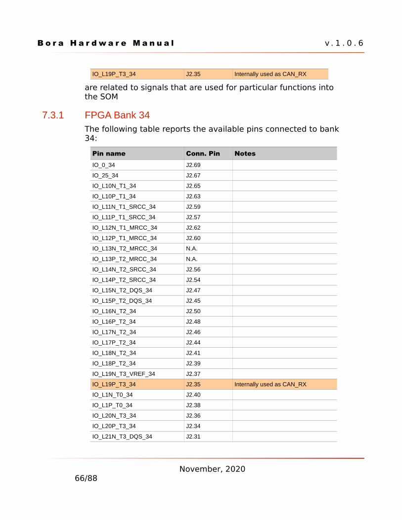
B o r a H a r d w a r e M a n u a l v . 1 . 0 . 6
IO_L19P_T3_34 J2.35 Internally used as CAN_RX
are related to signals that are used for particular functions into the SOM
7.3.1 FPGA Bank 34The following table reports the available pins connected to bank34:
Pin name Conn. Pin NotesIO_0_34 J2.69
IO_25_34 J2.67
IO_L10N_T1_34 J2.65
IO_L10P_T1_34 J2.63
IO_L11N_T1_SRCC_34 J2.59
IO_L11P_T1_SRCC_34 J2.57
IO_L12N_T1_MRCC_34 J2.62
IO_L12P_T1_MRCC_34 J2.60
IO_L13N_T2_MRCC_34 N.A.
IO_L13P_T2_MRCC_34 N.A.
IO_L14N_T2_SRCC_34 J2.56
IO_L14P_T2_SRCC_34 J2.54
IO_L15N_T2_DQS_34 J2.47
IO_L15P_T2_DQS_34 J2.45
IO_L16N_T2_34 J2.50
IO_L16P_T2_34 J2.48
IO_L17N_T2_34 J2.46
IO_L17P_T2_34 J2.44
IO_L18N_T2_34 J2.41
IO_L18P_T2_34 J2.39
IO_L19N_T3_VREF_34 J2.37
IO_L19P_T3_34 J2.35 Internally used as CAN_RX
IO_L1N_T0_34 J2.40
IO_L1P_T0_34 J2.38
IO_L20N_T3_34 J2.36
IO_L20P_T3_34 J2.34
IO_L21N_T3_DQS_34 J2.31
November, 202066/88
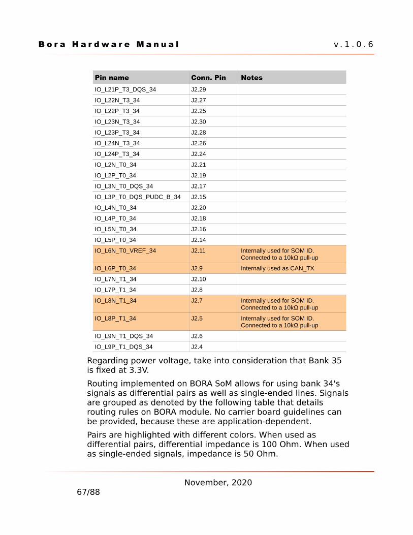
B o r a H a r d w a r e M a n u a l v . 1 . 0 . 6
Pin name Conn. Pin NotesIO_L21P_T3_DQS_34 J2.29
IO_L22N_T3_34 J2.27
IO_L22P_T3_34 J2.25
IO_L23N_T3_34 J2.30
IO_L23P_T3_34 J2.28
IO_L24N_T3_34 J2.26
IO_L24P_T3_34 J2.24
IO_L2N_T0_34 J2.21
IO_L2P_T0_34 J2.19
IO_L3N_T0_DQS_34 J2.17
IO_L3P_T0_DQS_PUDC_B_34 J2.15
IO_L4N_T0_34 J2.20
IO_L4P_T0_34 J2.18
IO_L5N_T0_34 J2.16
IO_L5P_T0_34 J2.14
IO_L6N_T0_VREF_34 J2.11 Internally used for SOM ID. Connected to a 10kΩ pull-up
IO_L6P_T0_34 J2.9 Internally used as CAN_TX
IO_L7N_T1_34 J2.10
IO_L7P_T1_34 J2.8
IO_L8N_T1_34 J2.7 Internally used for SOM ID. Connected to a 10kΩ pull-up
IO_L8P_T1_34 J2.5 Internally used for SOM ID. Connected to a 10kΩ pull-up
IO_L9N_T1_DQS_34 J2.6
IO_L9P_T1_DQS_34 J2.4
Regarding power voltage, take into consideration that Bank 35 is fixed at 3.3V.
Routing implemented on BORA SoM allows for using bank 34's signals as differential pairs as well as single-ended lines. Signalsare grouped as denoted by the following table that details routing rules on BORA module. No carrier board guidelines can be provided, because these are application-dependent.
Pairs are highlighted with different colors. When used as differential pairs, differential impedance is 100 Ohm. When usedas single-ended signals, impedance is 50 Ohm.
November, 202067/88
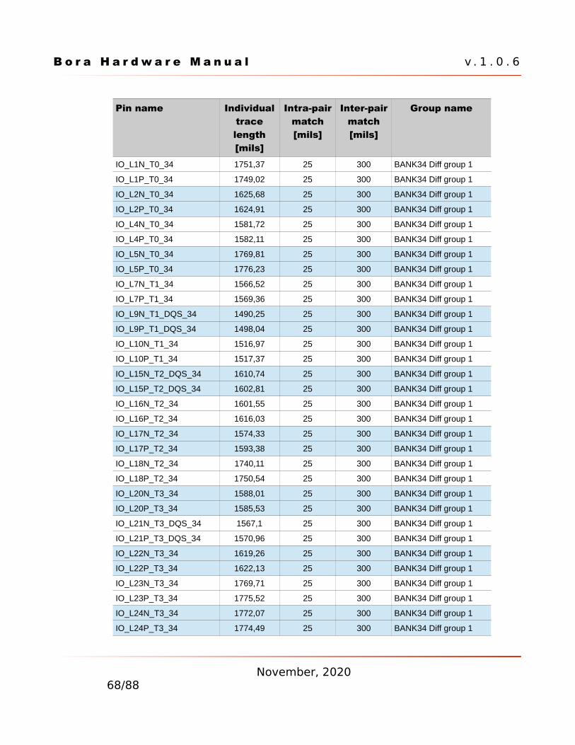
B o r a H a r d w a r e M a n u a l v . 1 . 0 . 6
Pin name Individualtracelength[mils]
Intra-pairmatch[mils]
Inter-pairmatch[mils]
Group name
IO_L1N_T0_34 1751,37 25 300 BANK34 Diff group 1
IO_L1P_T0_34 1749,02 25 300 BANK34 Diff group 1
IO_L2N_T0_34 1625,68 25 300 BANK34 Diff group 1
IO_L2P_T0_34 1624,91 25 300 BANK34 Diff group 1
IO_L4N_T0_34 1581,72 25 300 BANK34 Diff group 1
IO_L4P_T0_34 1582,11 25 300 BANK34 Diff group 1
IO_L5N_T0_34 1769,81 25 300 BANK34 Diff group 1
IO_L5P_T0_34 1776,23 25 300 BANK34 Diff group 1
IO_L7N_T1_34 1566,52 25 300 BANK34 Diff group 1
IO_L7P_T1_34 1569,36 25 300 BANK34 Diff group 1
IO_L9N_T1_DQS_34 1490,25 25 300 BANK34 Diff group 1
IO_L9P_T1_DQS_34 1498,04 25 300 BANK34 Diff group 1
IO_L10N_T1_34 1516,97 25 300 BANK34 Diff group 1
IO_L10P_T1_34 1517,37 25 300 BANK34 Diff group 1
IO_L15N_T2_DQS_34 1610,74 25 300 BANK34 Diff group 1
IO_L15P_T2_DQS_34 1602,81 25 300 BANK34 Diff group 1
IO_L16N_T2_34 1601,55 25 300 BANK34 Diff group 1
IO_L16P_T2_34 1616,03 25 300 BANK34 Diff group 1
IO_L17N_T2_34 1574,33 25 300 BANK34 Diff group 1
IO_L17P_T2_34 1593,38 25 300 BANK34 Diff group 1
IO_L18N_T2_34 1740,11 25 300 BANK34 Diff group 1
IO_L18P_T2_34 1750,54 25 300 BANK34 Diff group 1
IO_L20N_T3_34 1588,01 25 300 BANK34 Diff group 1
IO_L20P_T3_34 1585,53 25 300 BANK34 Diff group 1
IO_L21N_T3_DQS_34 1567,1 25 300 BANK34 Diff group 1
IO_L21P_T3_DQS_34 1570,96 25 300 BANK34 Diff group 1
IO_L22N_T3_34 1619,26 25 300 BANK34 Diff group 1
IO_L22P_T3_34 1622,13 25 300 BANK34 Diff group 1
IO_L23N_T3_34 1769,71 25 300 BANK34 Diff group 1
IO_L23P_T3_34 1775,52 25 300 BANK34 Diff group 1
IO_L24N_T3_34 1772,07 25 300 BANK34 Diff group 1
IO_L24P_T3_34 1774,49 25 300 BANK34 Diff group 1
November, 202068/88
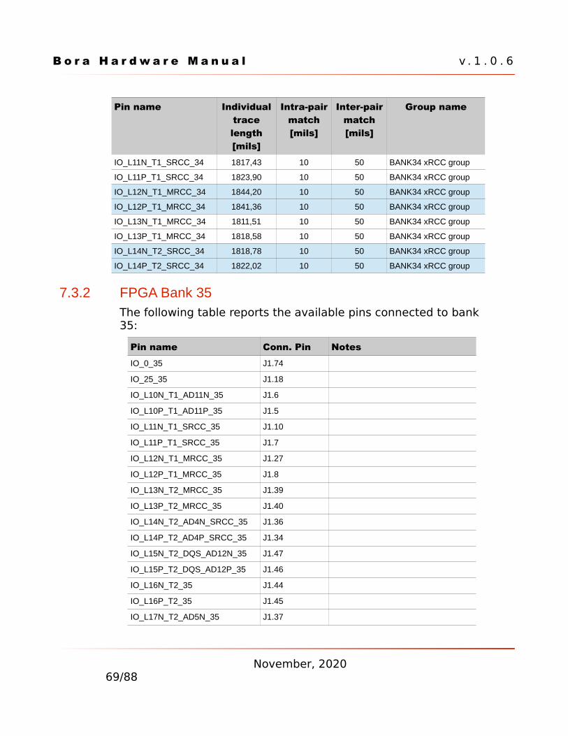
B o r a H a r d w a r e M a n u a l v . 1 . 0 . 6
Pin name Individualtracelength[mils]
Intra-pairmatch[mils]
Inter-pairmatch[mils]
Group name
IO_L11N_T1_SRCC_34 1817,43 10 50 BANK34 xRCC group
IO_L11P_T1_SRCC_34 1823,90 10 50 BANK34 xRCC group
IO_L12N_T1_MRCC_34 1844,20 10 50 BANK34 xRCC group
IO_L12P_T1_MRCC_34 1841,36 10 50 BANK34 xRCC group
IO_L13N_T1_MRCC_34 1811,51 10 50 BANK34 xRCC group
IO_L13P_T1_MRCC_34 1818,58 10 50 BANK34 xRCC group
IO_L14N_T2_SRCC_34 1818,78 10 50 BANK34 xRCC group
IO_L14P_T2_SRCC_34 1822,02 10 50 BANK34 xRCC group
7.3.2 FPGA Bank 35The following table reports the available pins connected to bank35:
Pin name Conn. Pin NotesIO_0_35 J1.74
IO_25_35 J1.18
IO_L10N_T1_AD11N_35 J1.6
IO_L10P_T1_AD11P_35 J1.5
IO_L11N_T1_SRCC_35 J1.10
IO_L11P_T1_SRCC_35 J1.7
IO_L12N_T1_MRCC_35 J1.27
IO_L12P_T1_MRCC_35 J1.8
IO_L13N_T2_MRCC_35 J1.39
IO_L13P_T2_MRCC_35 J1.40
IO_L14N_T2_AD4N_SRCC_35 J1.36
IO_L14P_T2_AD4P_SRCC_35 J1.34
IO_L15N_T2_DQS_AD12N_35 J1.47
IO_L15P_T2_DQS_AD12P_35 J1.46
IO_L16N_T2_35 J1.44
IO_L16P_T2_35 J1.45
IO_L17N_T2_AD5N_35 J1.37
November, 202069/88
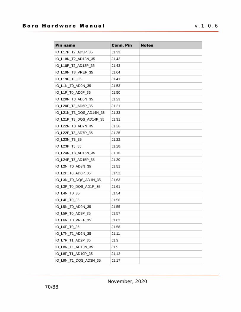
B o r a H a r d w a r e M a n u a l v . 1 . 0 . 6
Pin name Conn. Pin NotesIO_L17P_T2_AD5P_35 J1.32
IO_L18N_T2_AD13N_35 J1.42
IO_L18P_T2_AD13P_35 J1.43
IO_L19N_T3_VREF_35 J1.64
IO_L19P_T3_35 J1.41
IO_L1N_T0_AD0N_35 J1.53
IO_L1P_T0_AD0P_35 J1.50
IO_L20N_T3_AD6N_35 J1.23
IO_L20P_T3_AD6P_35 J1.21
IO_L21N_T3_DQS_AD14N_35 J1.33
IO_L21P_T3_DQS_AD14P_35 J1.31
IO_L22N_T3_AD7N_35 J1.26
IO_L22P_T3_AD7P_35 J1.25
IO_L23N_T3_35 J1.22
IO_L23P_T3_35 J1.28
IO_L24N_T3_AD15N_35 J1.16
IO_L24P_T3_AD15P_35 J1.20
IO_L2N_T0_AD8N_35 J1.51
IO_L2P_T0_AD8P_35 J1.52
IO_L3N_T0_DQS_AD1N_35 J1.63
IO_L3P_T0_DQS_AD1P_35 J1.61
IO_L4N_T0_35 J1.54
IO_L4P_T0_35 J1.56
IO_L5N_T0_AD9N_35 J1.55
IO_L5P_T0_AD9P_35 J1.57
IO_L6N_T0_VREF_35 J1.62
IO_L6P_T0_35 J1.58
IO_L7N_T1_AD2N_35 J1.11
IO_L7P_T1_AD2P_35 J1.3
IO_L8N_T1_AD10N_35 J1.9
IO_L8P_T1_AD10P_35 J1.12
IO_L9N_T1_DQS_AD3N_35 J1.17
November, 202070/88
B o r a H a r d w a r e M a n u a l v . 1 . 0 . 6
Pin name Conn. Pin NotesIO_L9P_T1_DQS_AD3P_35 J1.15
On BORA side, routing of bank 35 has been optimized to interface 16-bit DDR3 SDRAM memory devices, clocked at a maximum frequency of 400 MHz. Signals have been grouped in the following classes:
FDDR_ADDR
FDDR_CK
FDDR_BYTE0
FDDR_BYTE1
Some of them are differential pairs. These kind of signals are highlighted in dark gray in the following sections where, for each signal, detailed information are provided, related to routingrules implemented on BORA SoM and carrier board guidelines.
The tables in the following sections report general recommended rules for single-ended and differential pairs on carrier board in terms of impedance and isolation.
Regarding power voltage, Bank 35 is configurable and must be powered by carrier board.
Please note that some signals belonging to this bank can be configured alternatively as XADC auxiliary analog inputs.
7.3.2.1 Differential pairs
Value UOMCommon Mode impedance typ 55 Ohm
Differential Mode impedance typ 100 Ohm
Isolation 4x gap
7.3.2.2 Single-ended signals
Value UOMCommon Mode impedance typ 55 Ohm
Isolation 2x width
November, 202071/88
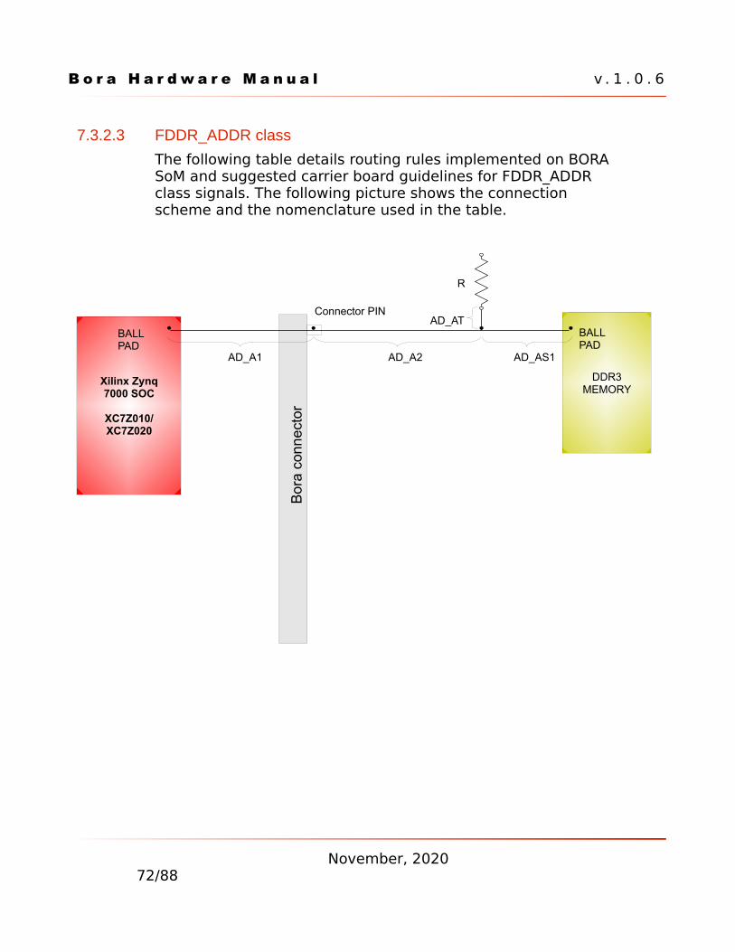
B o r a H a r d w a r e M a n u a l v . 1 . 0 . 6
7.3.2.3 FDDR_ADDR class
The following table details routing rules implemented on BORA SoM and suggested carrier board guidelines for FDDR_ADDR class signals. The following picture shows the connection scheme and the nomenclature used in the table.
November, 202072/88
Xilinx Zynq7000 SOC
XC7Z010/XC7Z020
Bo
ra c
onn
ect
or
DDR3MEMORY
BALL PAD
AD_A1 AD_A2
BALL PAD
AD_AS1
R
AD_ATConnector PIN
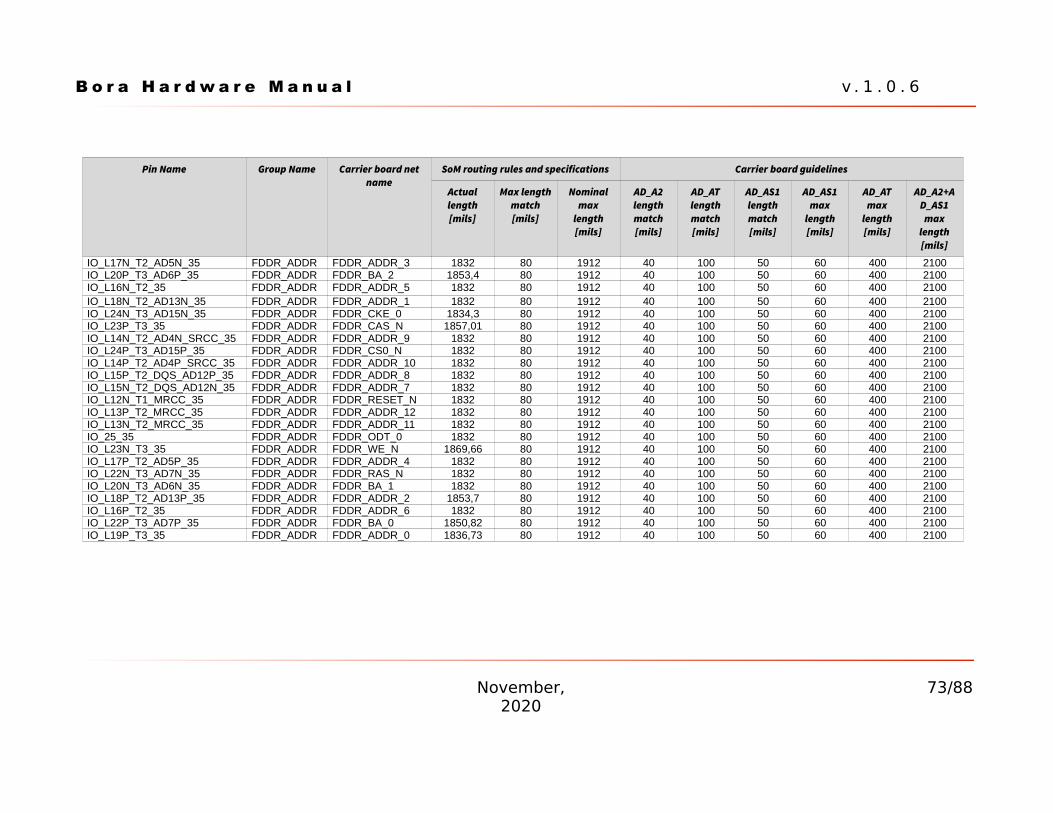
B o r a H a r d w a r e M a n u a l v . 1 . 0 . 6
Pin Name Group Name Carrier board netname
SoM routing rules and specifications Carrier board guidelines
Actuallength[mils]
Max lengthmatch[mils]
Nominalmax
length[mils]
AD_A2lengthmatch[mils]
AD_ATlengthmatch[mils]
AD_AS1lengthmatch[mils]
AD_AS1max
length[mils]
AD_ATmax
length[mils]
AD_A2+AD_AS1
maxlength[mils]
IO_L17N_T2_AD5N_35 FDDR_ADDR FDDR_ADDR_3 1832 80 1912 40 100 50 60 400 2100IO_L20P_T3_AD6P_35 FDDR_ADDR FDDR_BA_2 1853,4 80 1912 40 100 50 60 400 2100IO_L16N_T2_35 FDDR_ADDR FDDR_ADDR_5 1832 80 1912 40 100 50 60 400 2100IO_L18N_T2_AD13N_35 FDDR_ADDR FDDR_ADDR_1 1832 80 1912 40 100 50 60 400 2100IO_L24N_T3_AD15N_35 FDDR_ADDR FDDR_CKE_0 1834,3 80 1912 40 100 50 60 400 2100IO_L23P_T3_35 FDDR_ADDR FDDR_CAS_N 1857,01 80 1912 40 100 50 60 400 2100IO_L14N_T2_AD4N_SRCC_35 FDDR_ADDR FDDR_ADDR_9 1832 80 1912 40 100 50 60 400 2100IO_L24P_T3_AD15P_35 FDDR_ADDR FDDR_CS0_N 1832 80 1912 40 100 50 60 400 2100IO_L14P_T2_AD4P_SRCC_35 FDDR_ADDR FDDR_ADDR_10 1832 80 1912 40 100 50 60 400 2100IO_L15P_T2_DQS_AD12P_35 FDDR_ADDR FDDR_ADDR_8 1832 80 1912 40 100 50 60 400 2100IO_L15N_T2_DQS_AD12N_35 FDDR_ADDR FDDR_ADDR_7 1832 80 1912 40 100 50 60 400 2100IO_L12N_T1_MRCC_35 FDDR_ADDR FDDR_RESET_N 1832 80 1912 40 100 50 60 400 2100IO_L13P_T2_MRCC_35 FDDR_ADDR FDDR_ADDR_12 1832 80 1912 40 100 50 60 400 2100IO_L13N_T2_MRCC_35 FDDR_ADDR FDDR_ADDR_11 1832 80 1912 40 100 50 60 400 2100IO_25_35 FDDR_ADDR FDDR_ODT_0 1832 80 1912 40 100 50 60 400 2100IO_L23N_T3_35 FDDR_ADDR FDDR_WE_N 1869,66 80 1912 40 100 50 60 400 2100IO_L17P_T2_AD5P_35 FDDR_ADDR FDDR_ADDR_4 1832 80 1912 40 100 50 60 400 2100IO_L22N_T3_AD7N_35 FDDR_ADDR FDDR_RAS_N 1832 80 1912 40 100 50 60 400 2100IO_L20N_T3_AD6N_35 FDDR_ADDR FDDR_BA_1 1832 80 1912 40 100 50 60 400 2100IO_L18P_T2_AD13P_35 FDDR_ADDR FDDR_ADDR_2 1853,7 80 1912 40 100 50 60 400 2100IO_L16P_T2_35 FDDR_ADDR FDDR_ADDR_6 1832 80 1912 40 100 50 60 400 2100IO_L22P_T3_AD7P_35 FDDR_ADDR FDDR_BA_0 1850,82 80 1912 40 100 50 60 400 2100IO_L19P_T3_35 FDDR_ADDR FDDR_ADDR_0 1836,73 80 1912 40 100 50 60 400 2100
November,2020
73/88
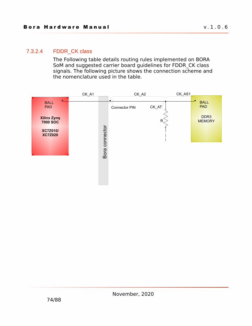
B o r a H a r d w a r e M a n u a l v . 1 . 0 . 6
7.3.2.4 FDDR_CK class
The Following table details routing rules implemented on BORA SoM and suggested carrier board guidelines for FDDR_CK class signals. The following picture shows the connection scheme andthe nomenclature used in the table.
November, 202074/88
Xilinx Zynq7000 SOC
XC7Z010/XC7Z020
Bo
ra c
onn
ect
or
DDR3MEMORY
BALL PAD
CK_A1 CK_A2
BALL PAD
CK_AS1
R
CK_ATConnector PIN
B o r a H a r d w a r e M a n u a l v . 1 . 0 . 6
Pin Name Group Name Carrier boardnet name
SoM routing rules and specifications Carrier board guidelines
Actuallength[mils]
Intra-pair
match[mils]
Maxlength
match(1
)[mils]
Nominalmax
length[mils]
Intra-pair
match[mils]
CK_A2pair
match(2)
[mils]
CK_ATintra-pair
match[mils]
CK_AS1match
(2)[mils]
CK_AS1max
length[mils]
CK_ATmaximu
mlength[mils]
CK_ATpair
match(2)
[mils]
CK_A2+CK_AS1
maxlength[mils]
IO_L21P_T3_DQS_AD14P_35
FDDR_CK FDDR_CK_P0 1900,39 5 80 1912 10 40 5 50 60 400 100 2100
IO_L21N_T3_DQS_AD14N_35
FDDR_CK FDDR_CK_N0 1898,17 5 80 1912 10 40 5 50 60 400 100 2100
1: with respect to FDDR_ADDR group2: with respect to FDDR_ADDR
7.3.2.5 FDDR_BYTE0 class
The following table details routing rules implemented on BORA SoM and suggested carrier board guidelines for FDDR_BYTE0 class signals.
Pin Name Group name Carrier board netname
SoM routing rules and specifications Carrier board guidelines
Actuallength[mils]
Maxlengthmatch[mils]
Max inter-pairmatch length
on SOM[mils]
Nominalmax length
[mils]
Group match(mandatory)
[mils]
Intra-pairmatch
(mandatory)[mils]
Max length[mils]
IO_L2N_T0_AD8N_35 FDDR_BYTE0 FDDR_DQ_2 1222,66 15 - 1230 25 - CK_A2+CK_AS1(max)IO_L6P_T0_35 FDDR_BYTE0 FDDR_DQ_7 1219,68 15 - 1230 25 - CK_A2+CK_AS1(max)IO_L5P_T0_AD9P_35 FDDR_BYTE0 FDDR_DQ_5 1226,42 15 - 1230 25 - CK_A2+CK_AS1(max)IO_L4P_T0_35 FDDR_BYTE0 FDDR_DQ_3 1219,68 15 - 1230 25 - CK_A2+CK_AS1(max)IO_L2P_T0_AD8P_35 FDDR_BYTE0 FDDR_DQ_1 1219,68 15 - 1230 25 - CK_A2+CK_AS1(max)IO_L1N_T0_AD0N_35 FDDR_BYTE0 FDDR_DQ_0 1219,68 15 - 1230 25 - CK_A2+CK_AS1(max)IO_L4N_T0_35 FDDR_BYTE0 FDDR_DQ_4 1219,68 15 - 1230 25 - CK_A2+CK_AS1(max)IO_L5N_T0_AD9N_35 FDDR_BYTE0 FDDR_DQ_6 1219,68 15 - 1230 25 - CK_A2+CK_AS1(max)IO_L1P_T0_AD0P_35 FDDR_BYTE0 FDDR_DM_0 1219,68 15 - 1230 25 - CK_A2+CK_AS1(max)IO_L3P_T0_DQS_AD1P_35 FDDR_BYTE0 FDDR_DQS_P0 1221,04 15 5 1230 25 5 CK_A2+CK_AS1(max)
November,2020
75/88
B o r a H a r d w a r e M a n u a l v . 1 . 0 . 6
Pin Name Group name Carrier board netname
SoM routing rules and specifications Carrier board guidelines
Actuallength[mils]
Maxlengthmatch[mils]
Max inter-pairmatch length
on SOM[mils]
Nominalmax length
[mils]
Group match(mandatory)
[mils]
Intra-pairmatch
(mandatory)[mils]
Max length[mils]
IO_L3N_T0_DQS_AD1N_35 FDDR_BYTE0 FDDR_DQS_N0 1219,42 15 5 1230 25 5 CK_A2+CK_AS1(max)
7.3.2.6 FDDR_BYTE1 class
The following table details routing rules implemented on BORA SoM and suggested carrier board guidelines for FDDR_BYTE1 class signals.
Pin Name Group name Carrier board netname
SoM routing rules and specifications Carrier board guidelines
Actuallength[mils]
Maxlengthmatch[mils]
Max inter-pairmatch length
on SOM[mils]
Nominalmax length
[mils]
Group match(mandatory)
[mils]
Intra-pairmatch
(mandatory)[mils]
Max length[mils]
IO_L10N_T1_AD11N_35 FDDR_BYTE1 FDDR_DQ_12 1345,93 15 - 1355 20 - CK_A2+CK_AS1(max)IO_L10P_T1_AD11P_35 FDDR_BYTE1 FDDR_DQ_11 1345,93 15 - 1355 20 - CK_A2+CK_AS1(max)IO_L11P_T1_SRCC_35 FDDR_BYTE1 FDDR_DQ_13 1353,43 15 - 1355 20 - CK_A2+CK_AS1(max)IO_L12P_T1_MRCC_35 FDDR_BYTE1 FDDR_DQ_15 1341,3 15 - 1355 20 - CK_A2+CK_AS1(max)IO_L11N_T1_SRCC_35 FDDR_BYTE1 FDDR_DQ_14 1340 15 - 1355 20 - CK_A2+CK_AS1(max)IO_L8P_T1_AD10P_35 FDDR_BYTE1 FDDR_DQ_9 1340 15 - 1355 20 - CK_A2+CK_AS1(max)IO_L7N_T1_AD2N_35 FDDR_BYTE1 FDDR_DQ_8 1340 15 - 1355 20 - CK_A2+CK_AS1(max)IO_L8N_T1_AD10N_35 FDDR_BYTE1 FDDR_DQ_10 1340 15 - 1355 20 - CK_A2+CK_AS1(max)IO_L7P_T1_AD2P_35 FDDR_BYTE1 FDDR_DM_1 1345,93 15 - 1355 20 - CK_A2+CK_AS1(max)IO_L9P_T1_DQS_AD3P_35 FDDR_BYTE1 FDDR_DQS_P1 1354,26 15 5 1355 20 5 CK_A2+CK_AS1(max)IO_L9N_T1_DQS_AD3N_35 FDDR_BYTE1 FDDR_DQS_N1 1350,66 15 5 1355 20 5 CK_A2+CK_AS1(max)
November,2020
76/88
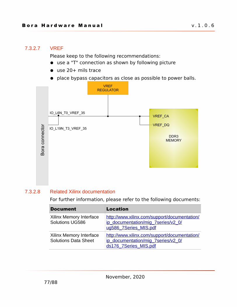
B o r a H a r d w a r e M a n u a l v . 1 . 0 . 6
7.3.2.7 VREF
Please keep to the following recommendations: use a "T" connection as shown by following picture
use 20+ mils trace
place bypass capacitors as close as possible to power balls.
7.3.2.8 Related Xilinx documentation
For further information, please refer to the following documents:
Document LocationXilinx Memory Interface Solutions UG586
http://www.xilinx.com/support/documentation/ip_documentation/mig_7series/v2_0/ug586_7Series_MIS.pdf
Xilinx Memory Interface Solutions Data Sheet
http://www.xilinx.com/support/documentation/ip_documentation/mig_7series/v2_0/ds176_7Series_MIS.pdf
November, 202077/88
Bo
ra c
on
nect
or
VREFREGULATOR
DDR3MEMORY
IO_L19N_T3_VREF_35
VREF_CAIO_L6N_T0_VREF_35
VREF_DQ
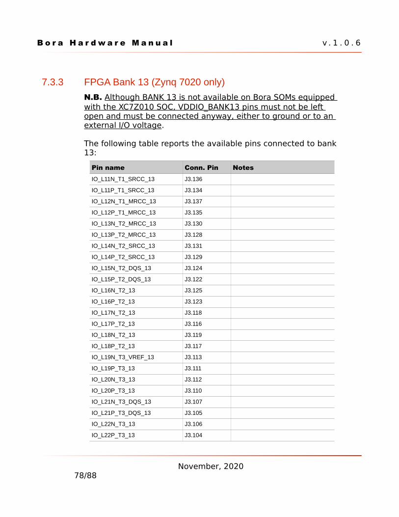
B o r a H a r d w a r e M a n u a l v . 1 . 0 . 6
7.3.3 FPGA Bank 13 (Zynq 7020 only)
N.B. Although BANK 13 is not available on Bora SOMs equipped with the XC7Z010 SOC, VDDIO_BANK13 pins must not be left open and must be connected anyway, either to ground or to an external I/O voltage.
The following table reports the available pins connected to bank13:
Pin name Conn. Pin NotesIO_L11N_T1_SRCC_13 J3.136
IO_L11P_T1_SRCC_13 J3.134
IO_L12N_T1_MRCC_13 J3.137
IO_L12P_T1_MRCC_13 J3.135
IO_L13N_T2_MRCC_13 J3.130
IO_L13P_T2_MRCC_13 J3.128
IO_L14N_T2_SRCC_13 J3.131
IO_L14P_T2_SRCC_13 J3.129
IO_L15N_T2_DQS_13 J3.124
IO_L15P_T2_DQS_13 J3.122
IO_L16N_T2_13 J3.125
IO_L16P_T2_13 J3.123
IO_L17N_T2_13 J3.118
IO_L17P_T2_13 J3.116
IO_L18N_T2_13 J3.119
IO_L18P_T2_13 J3.117
IO_L19N_T3_VREF_13 J3.113
IO_L19P_T3_13 J3.111
IO_L20N_T3_13 J3.112
IO_L20P_T3_13 J3.110
IO_L21N_T3_DQS_13 J3.107
IO_L21P_T3_DQS_13 J3.105
IO_L22N_T3_13 J3.106
IO_L22P_T3_13 J3.104
November, 202078/88
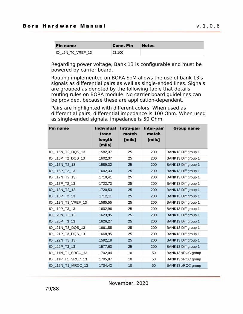
B o r a H a r d w a r e M a n u a l v . 1 . 0 . 6
Pin name Conn. Pin NotesIO_L6N_T0_VREF_13 J3.100
Regarding power voltage, Bank 13 is configurable and must be powered by carrier board.
Routing implemented on BORA SoM allows the use of bank 13's signals as differential pairs as well as single-ended lines. Signalsare grouped as denoted by the following table that details routing rules on BORA module. No carrier board guidelines can be provided, because these are application-dependent.
Pairs are highlighted with different colors. When used as differential pairs, differential impedance is 100 Ohm. When usedas single-ended signals, impedance is 50 Ohm.
Pin name Individualtracelength[mils]
Intra-pairmatch[mils]
Inter-pairmatch[mils]
Group name
IO_L15N_T2_DQS_13 1582,37 25 200 BANK13 Diff group 1
IO_L15P_T2_DQS_13 1602,37 25 200 BANK13 Diff group 1
IO_L16N_T2_13 1589,32 25 200 BANK13 Diff group 1
IO_L16P_T2_13 1602,33 25 200 BANK13 Diff group 1
IO_L17N_T2_13 1710,41 25 200 BANK13 Diff group 1
IO_L17P_T2_13 1722,73 25 200 BANK13 Diff group 1
IO_L18N_T2_13 1720,53 25 200 BANK13 Diff group 1
IO_L18P_T2_13 1712,11 25 200 BANK13 Diff group 1
IO_L19N_T3_VREF_13 1585,55 25 200 BANK13 Diff group 1
IO_L19P_T3_13 1602,96 25 200 BANK13 Diff group 1
IO_L20N_T3_13 1623,95 25 200 BANK13 Diff group 1
IO_L20P_T3_13 1626,27 25 200 BANK13 Diff group 1
IO_L21N_T3_DQS_13 1661,55 25 200 BANK13 Diff group 1
IO_L21P_T3_DQS_13 1668,95 25 200 BANK13 Diff group 1
IO_L22N_T3_13 1592,18 25 200 BANK13 Diff group 1
IO_L22P_T3_13 1577,63 25 200 BANK13 Diff group 1
IO_L11N_T1_SRCC_13 1702,04 10 50 BANK13 xRCC group
IO_L11P_T1_SRCC_13 1705,07 10 50 BANK13 xRCC group
IO_L12N_T1_MRCC_13 1704,42 10 50 BANK13 xRCC group
November, 202079/88
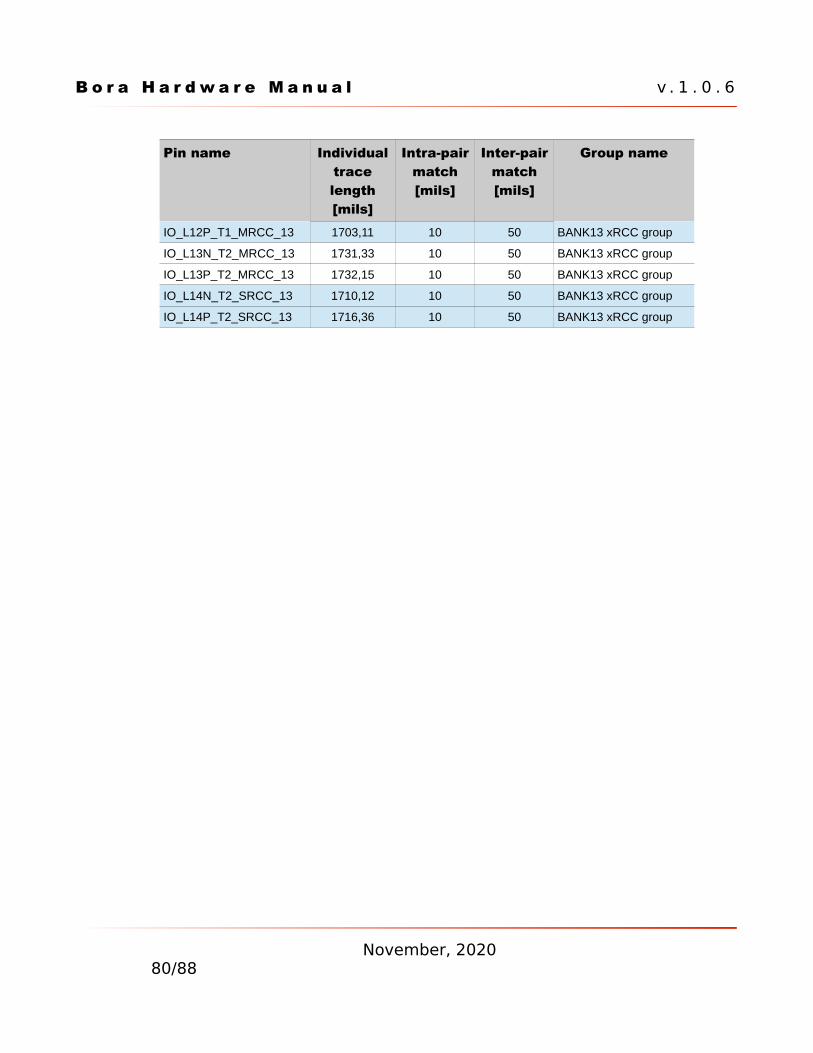
B o r a H a r d w a r e M a n u a l v . 1 . 0 . 6
Pin name Individualtracelength[mils]
Intra-pairmatch[mils]
Inter-pairmatch[mils]
Group name
IO_L12P_T1_MRCC_13 1703,11 10 50 BANK13 xRCC group
IO_L13N_T2_MRCC_13 1731,33 10 50 BANK13 xRCC group
IO_L13P_T2_MRCC_13 1732,15 10 50 BANK13 xRCC group
IO_L14N_T2_SRCC_13 1710,12 10 50 BANK13 xRCC group
IO_L14P_T2_SRCC_13 1716,36 10 50 BANK13 xRCC group
November, 202080/88
B o r a H a r d w a r e M a n u a l v . 1 . 0 . 6
8 Carrier board design guidelinesGenerally speaking, when designing a system-on-module (SoM) product it is impossible to know in advance the combination of interfaces and functionalities that will be implemented by the system integrator. This is even more true in case of BORA, due to the unprecedented flexibility and versatility of Zynq architecture. For this reason, BORA implements advanced routing schemes that, in combination with proper carrier board design, allow the implementation of high-speed complex interfaces that satisfy signal integrity requirements.
This chapter describes in detail such schemes and provides carrier board design guidelines accordingly. These information complement SoM-independent recommendations provided in http://wiki.dave.eu/index.php/Carrier_board_design_guidelines_(SOM).
In the following section the terms "Inter-pair matching" and "Intra-pair matching" are used. They indicate respectively:
length matching among pairs belonging to the same class or group
length matching between traces belonging to the same pair.
8.1 Suggested PCB specificationsMin Typ
Layers (number) 4 6
GND Plane Layers 1 2
Power Plane Layers 1 1
Vias hole (mechanical)4 [mm] 0.3 -
8.2 Power railsFollowing power rails should be kept as short as possible and should be sized in order to minimize IR drop at maximum estimated current:
4 Smaller holes are deprecated because of their limited current capacity and heat dissipation.
November, 202081/88
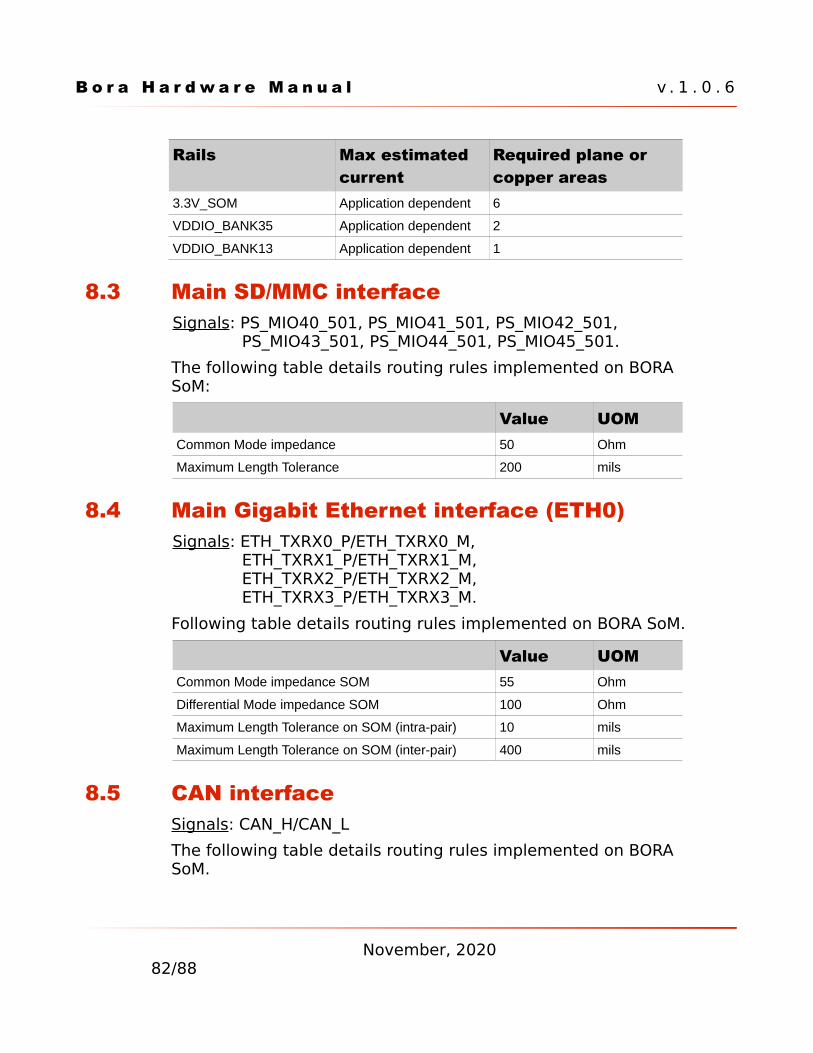
B o r a H a r d w a r e M a n u a l v . 1 . 0 . 6
Rails Max estimated current
Required plane or copper areas
3.3V_SOM Application dependent 6
VDDIO_BANK35 Application dependent 2
VDDIO_BANK13 Application dependent 1
8.3 Main SD/MMC interfaceSignals: PS_MIO40_501, PS_MIO41_501, PS_MIO42_501,
PS_MIO43_501, PS_MIO44_501, PS_MIO45_501.
The following table details routing rules implemented on BORA SoM:
Value UOMCommon Mode impedance 50 Ohm
Maximum Length Tolerance 200 mils
8.4 Main Gigabit Ethernet interface (ETH0)Signals: ETH_TXRX0_P/ETH_TXRX0_M,
ETH_TXRX1_P/ETH_TXRX1_M, ETH_TXRX2_P/ETH_TXRX2_M, ETH_TXRX3_P/ETH_TXRX3_M.
Following table details routing rules implemented on BORA SoM.
Value UOMCommon Mode impedance SOM 55 Ohm
Differential Mode impedance SOM 100 Ohm
Maximum Length Tolerance on SOM (intra-pair) 10 mils
Maximum Length Tolerance on SOM (inter-pair) 400 mils
8.5 CAN interfaceSignals: CAN_H/CAN_L
The following table details routing rules implemented on BORA SoM.
November, 202082/88
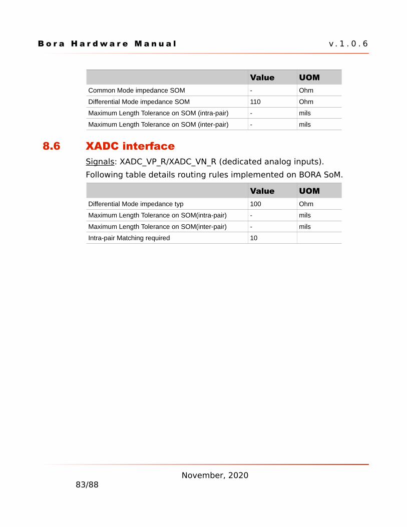
B o r a H a r d w a r e M a n u a l v . 1 . 0 . 6
Value UOMCommon Mode impedance SOM - Ohm
Differential Mode impedance SOM 110 Ohm
Maximum Length Tolerance on SOM (intra-pair) - mils
Maximum Length Tolerance on SOM (inter-pair) - mils
8.6 XADC interfaceSignals: XADC_VP_R/XADC_VN_R (dedicated analog inputs).
Following table details routing rules implemented on BORA SoM.
Value UOMDifferential Mode impedance typ 100 Ohm
Maximum Length Tolerance on SOM(intra-pair) - mils
Maximum Length Tolerance on SOM(inter-pair) - mils
Intra-pair Matching required 10
November, 202083/88
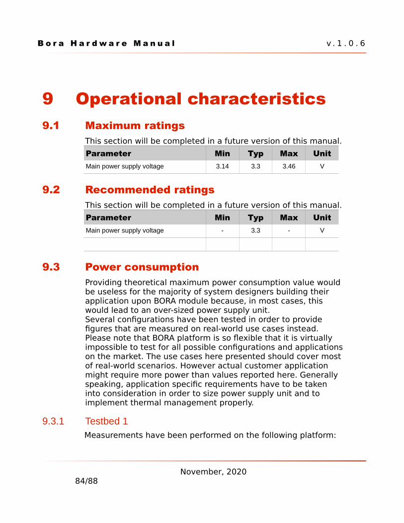
B o r a H a r d w a r e M a n u a l v . 1 . 0 . 6
9 Operational characteristics9.1 Maximum ratings
This section will be completed in a future version of this manual.
Parameter Min Typ Max UnitMain power supply voltage 3.14 3.3 3.46 V
9.2 Recommended ratingsThis section will be completed in a future version of this manual.
Parameter Min Typ Max UnitMain power supply voltage - 3.3 - V
9.3 Power consumptionProviding theoretical maximum power consumption value would be useless for the majority of system designers building their application upon BORA module because, in most cases, this would lead to an over-sized power supply unit.Several configurations have been tested in order to provide figures that are measured on real-world use cases instead. Please note that BORA platform is so flexible that it is virtually impossible to test for all possible configurations and applicationson the market. The use cases here presented should cover mostof real-world scenarios. However actual customer application might require more power than values reported here. Generally speaking, application specific requirements have to be taken into consideration in order to size power supply unit and to implement thermal management properly.
9.3.1 Testbed 1Measurements have been performed on the following platform:
November, 202084/88
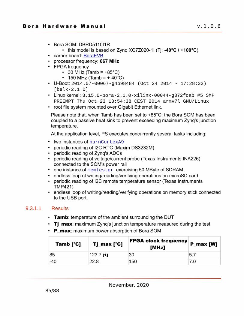
B o r a H a r d w a r e M a n u a l v . 1 . 0 . 6
• Bora SOM: DBRD5110I1R • this model is based on Zynq XC7Z020-1I (Tj: -40°C / +100°C)
• carrier board: BoraEVB • processor frequency: 667 MHz • FPGA frequency
• 30 MHz (Tamb = +85°C) • 150 MHz (Tamb = +-40°C)
• U-Boot: 2014.07-00067-g4b98484 (Oct 24 2014 - 17:28:32) [belk-2.1.0]
• Linux kernel: 3.15.0-bora-2.1.0-xilinx-00044-g372fcab #5 SMP PREEMPT Thu Oct 23 13:54:38 CEST 2014 armv7l GNU/Linux
• root file system mounted over Gigabit Ethernet link.
Please note that, when Tamb has been set to +85°C, the Bora SOM has been coupled to a passive heat sink to prevent exceeding maximum Zynq's junction temperature.
At the application level, PS executes concurrently several tasks including:
• two instances of burnCortexA9 • periodic reading of I2C RTC (Maxim DS3232M) • periodic reading of Zynq's ADCs • periodic reading of voltage/current probe (Texas Instruments INA226)
connected to the SOM's power rail • one instance of memtester, exercising 50 MByte of SDRAM • endless loop of writing/reading/verifying operations on microSD card • periodic reading of I2C remote temperature sensor (Texas Instruments
TMP421) • endless loop of writing/reading/verifying operations on memory stick connected
to the USB port.
9.3.1.1 Results
• Tamb: temperature of the ambient surrounding the DUT
• Tj_max: maximum Zynq's junction temperature measured during the test
• P_max: maximum power absorption of Bora SOM
Tamb [°C] Tj_max [°C] FPGA clock frequency
[MHz] P_max [W]
85 123.7 [1] 30 5.7
-40 22.8 150 7.0
November, 202085/88
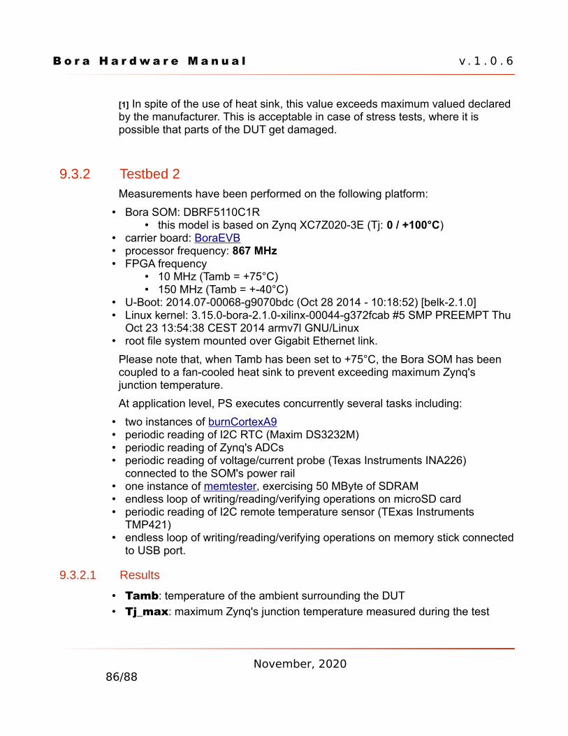
B o r a H a r d w a r e M a n u a l v . 1 . 0 . 6
[1] In spite of the use of heat sink, this value exceeds maximum valued declared by the manufacturer. This is acceptable in case of stress tests, where it is possible that parts of the DUT get damaged.
9.3.2 Testbed 2Measurements have been performed on the following platform:
• Bora SOM: DBRF5110C1R • this model is based on Zynq XC7Z020-3E (Tj: 0 / +100°C)
• carrier board: BoraEVB • processor frequency: 867 MHz • FPGA frequency
• 10 MHz (Tamb = +75°C) • 150 MHz (Tamb = +-40°C)
• U-Boot: 2014.07-00068-g9070bdc (Oct 28 2014 - 10:18:52) [belk-2.1.0] • Linux kernel: 3.15.0-bora-2.1.0-xilinx-00044-g372fcab #5 SMP PREEMPT Thu
Oct 23 13:54:38 CEST 2014 armv7l GNU/Linux • root file system mounted over Gigabit Ethernet link.
Please note that, when Tamb has been set to +75°C, the Bora SOM has been coupled to a fan-cooled heat sink to prevent exceeding maximum Zynq's junction temperature.
At application level, PS executes concurrently several tasks including:
• two instances of burnCortexA9 • periodic reading of I2C RTC (Maxim DS3232M) • periodic reading of Zynq's ADCs • periodic reading of voltage/current probe (Texas Instruments INA226)
connected to the SOM's power rail • one instance of memtester, exercising 50 MByte of SDRAM • endless loop of writing/reading/verifying operations on microSD card • periodic reading of I2C remote temperature sensor (TExas Instruments
TMP421) • endless loop of writing/reading/verifying operations on memory stick connected
to USB port.
9.3.2.1 Results
• Tamb: temperature of the ambient surrounding the DUT
• Tj_max: maximum Zynq's junction temperature measured during the test
November, 202086/88
B o r a H a r d w a r e M a n u a l v . 1 . 0 . 6
• P_max: maximum power absorption of Bora SOM
Tamb [°C] Tj_max [°C] FPGA clock frequency
[MHz] P_max [W]
75 100.8 10 4.1
-40 34.7 150 7.3
9.4 Heat Dissipation
Bora product is designed to support the maximum available temperature range declared by the manufacturer.
The customer shall define and conduct a reasonable number of tests and verification in order to qualify the DUT capabilities to manage the heat dissipation.
For example, in the previous test cases:
• Testbed 1 : when Tamb has been set to +85°C, the Bora SOM has been coupled to a passive heat sink to prevent exceeding maximum Zynq's junction temperature
• Testbed 2 : when Tamb has been set to +75°C, the Bora SOM has been coupled to a fan-cooled heat sink to prevent exceeding maximum Zynq's junction temperature
Any heatsink, fan etc shall be defined case by case depending on the various use conditions like: air cooling (forced or not), enclosure dimensions, mechanical/thermal coupling with heatsink.
A proper thermal analysis must be investigated on the real use scenario which depends on FPGA design, frequency configurations, working signals, etc.
November, 202087/88
B o r a H a r d w a r e M a n u a l v . 1 . 0 . 6
10 Application notesPlease refer to the following documents available on DAVE Embedded Systems Developers Wiki:
Document LocationIntegration Guide http://wiki.dave.eu/index.php/
Integration_guide_%28Bora%29
Carrier board design guidelines
http://wiki.dave.eu/index.php/Carrier_board_design_guidelines_%28SOM%29
BELK application notes http://wiki.dave.eu/index.php/Application_Notes_%28Bora%29
November, 202088/88
Mouser Electronics
Authorized Distributor
Click to View Pricing, Inventory, Delivery & Lifecycle Information: DAVE Embedded Systems:
DBRF5110C