Embed Size (px)
Citation preview
BACHELOR’S THESIS
Bachelor's Degree in Industrial Electronics and Automatic Control
Engineering
FPGA-BASED ACCELERATOR FOR CONVOLUTIONAL
NEURAL NETWORKS
Report and annexes
Author: Noelia Cívico Dorado Director: Professor Nader Bagherzadeh Department: EECS, UCI Quarter: Spring 2020

FPGA-Based Accelerator for Convolutional Neural Networks Abstract
i
Abstract
In recent years, hardware architecture and system design have become relevant research areas for
artificial intelligence in terms of innovation and efficiency. This growing popularity leads to increasing
interest in Convolutional Neural Networks (CNNs), due to its high accuracy and applicability, ranging
from facial and speech recognition to image classification and segmentation. CNNs are a class of deep
neural network (DNN), which use convolution instead of general matrix multiplication in at least one
of their layers. Their intense computational demand requires the implementation of hardware
accelerators for boosting their performance. Hardware acceleration consist of using computer
hardware specially made to perform some functions more efficiently than is possible in software
running on a general-purpose central processing unit (CPU).
Field-programmable devices (FPGAs) represent an interesting solution for dealing with CNNs power
consumption and memory footprint constraints. FPGAs high energy efficiency, computing capabilities
and reconfigurability offer a strong ground for meeting CNNs latency, accuracy and complexity
requirements.
The aim of this project is to design a FPGA-based accelerator for CNNs, which presents good energy-
efficiency and high-speed results. The work presented in this report is focused on the implementation
of a two-dimensional 16-bit fixed-point hardware convolver with the capability of computing arbitrary-
size 2-D convolutions and performing single-cycle multiply-and-accumulate operations.
In order to design and implement the convolver unit, which will constitute the core block of the CNN
hardware accelerator, the adopted approach is based on a strategy to extract windows of pixels from
a single data stream.
This study involves the use of different FPGA families by Xilinx, analyzing design portability on devices
with different sizes and performances. Promising comparative results have been achieved by
optimizing the original convolver model and comparing it with other reference designs.
FPGA-Based Accelerator for Convolutional Neural Networks Resum
ii
Resum
En aquests darrers anys, l’arquitectura hardware i el disseny de nous sistemes s’han convertit en àrees
de recerca predominants en el món de la intel·ligència artificial en termes d’innovació i eficiència.
Aquest increment de popularitat es tradueix en un interès creixent per l’àmbit de les Xarxes Neuronals
Convolucionals (l’acrònim anglès és CNN), a causa de la seva alta precisió i aplicabilitat, que varia des
del reconeixement facial i de veu a la classificació i segmentació d'imatges. Les CNNs són una classe de
xarxa neuronal profunda (l’acrònim anglès és DNN), que utilitzen la convolució en lloc de la
multiplicació de matrius general en almenys una de les seves capes. La seva intensa demanda
computacional requereix la implementació d'acceleradors hardware per augmentar el seu rendiment.
L’acceleració hardware consisteix en utilitzar hardware específic per realitzar algunes funcions amb
més eficiència del que és possible en el software que s’executa en una unitat de processament central
(l’acrònim anglès és CPU) de propòsit general.
Les matrius de portes programables (l’acrònim anglès és FPGA) representen una solució interessant
per afrontar les limitacions de consum d’energia i petjada de memòria en les CNNs. L’alta eficiència
energètica, i la capacitat de computació i de reconfiguració de les FPGAs ofereixen una base sòlida per
l’assoliment dels requisits de latència, precisió i complexitat de les CNNs.
L'objectiu d'aquest projecte és el disseny d’un accelerador de xarxes neuronals convolucionals basat
en una matriu de portes programables, que presenti bons resultats en relació al consum d’energia i
l’alta-velocitat. El treball presentat en aquest informe està centrat en la implementació d'una unitat de
convolució bidimensional de 16 bits amb representació de coma fixa, que compta amb la capacitat de
calcular convolucions bidimensional de mides arbitràries i de realitzar operacions de multiplicació-i-
acumulació en un únic cicle de rellotge.
Amb l’objectiu de dissenyar i implementar la unitat de convolució, la qual constituirà el bloc principal
de l'accelerador hardware de CNNs, la proposta plantejada es basa en una estratègia per extreure
finestres de píxels a partir d’un únic flux de dades.
Aquest estudi inclou l'ús de diferents famílies de FPGAs de Xilinx, entre les quals es realitza un anàlisi
de la portabilitat del disseny en dispositius amb diferents mides i prestacions. Els resultats obtinguts
mitjançant l’optimització del model original i la comparació amb altres dissenys de referència són molt
favorables.
FPGA-Based Accelerator for Convolutional Neural Networks Resumen
iii
Resumen
En los últimos años, la arquitectura hardware y el diseño de nuevos sistemas se han convertido en
áreas de investigación relevantes en el mundo de la inteligencia artificial en términos de innovación y
eficiencia. Esta creciente popularidad se traduce en un creciente interés por las Redes Neuronales
Convolucionales (el acrónimo inglés es CNN), debido a su alta precisión y aplicabilidad, que va desde el
reconocimiento facial y del habla hasta la clasificación y segmentación de imágenes. Las CNNs son una
clase de red neuronal profunda (el acrónimo inglés es DNN), que utilizan la convolución en lugar de la
multiplicación de matrices general en al menos una de sus capas. Su intensa demanda computacional
requiere la implementación de aceleradores de hardware para aumentar su rendimiento. La
aceleración de hardware consiste en usar hardware específico para realizar algunas funciones de
manera más eficiente de lo que es posible en el software que se ejecuta en una unidad central de
procesamiento (el acrónimo inglés es CPU) de propósito general.
Las matrices de puertas lógicas programables (el acrónimo en inglés es FPGA) representan una solución
interesante para lidiar con el consumo de energía y las limitaciones de huella de memoria de las CNNs.
La alta eficiencia energética, y las capacidades computacionales y de reconfiguración de las FPGAs
ofrecen una base sólida para cumplir con los requisitos de latencia, precisión y complejidad de las
CNNs.
El objetivo de este proyecto es diseñar un acelerador de redes neuronales convolucionales basado en
una matriz de puertas lógicas programables, que presente buenos resultados de eficiencia energética
y alta-velocidad. El trabajo presentado en este informe se centra en la implementación de una unidad
de convolución hardware bidimensional de 16 bits con representación de coma fija, que cuenta con la
capacidad de calcular convoluciones bidimensionales de tamaño arbitrario y realizar operaciones de
multiplicación-y-acumulación de ciclo único.
Para diseñar e implementar la unidad de convolución, que constituirá el bloque central del acelerador
de hardware de CNNs, la propuesta adoptada se basa en una estrategia para extraer ventanas de
píxeles de un solo flujo de datos.
Este estudio incluye el uso de diferentes familias de FPGAs de Xilinx, entre las cuales se realiza un
análisis de la portabilidad del diseño en dispositivos con diferentes tamaños y prestaciones. Se han
logrado resultados comparativos prometedores al optimizar el modelo original y compararlo con otros
diseños de referencia.
FPGA-Based Accelerator for Convolutional Neural Networks Acknowledgments
iv
Acknowledgments
First of all, I would like to deeply thank my supervisor, Professor Nader Bagherzadeh, for giving me the
opportunity of being part of his lab. Thank you for your valuable advice and guidance, as well as for the
chance to broaden my knowledge in the field of Artificial Intelligence.
Furthermore, I would like to thank PhD Min Soo Kim and PhD Masoomeh Jasemi for their continuous
support. Your valuable knowledge and your willingness to help with any technical difficulties have been
essential for the development of my thesis.
Moreover, I would like to thank Professor Roger H. Rangel for providing me the opportunity of coming
to the University of California, Irvine with the Balsells Fellowship.
I am also very grateful to my university, EEBE – UPC, for teaching me the necessary theoretical
background, which allows me to develop this and many other projects throughout my future career.
Last but not least, I would like to express my deepest gratitude to my family and friends, especially to
my parents and my sister. Thank you, mom and dad, for your unconditional support and for always
encouraging me to pursue my dreams. And thank you Marina for our countless laughs and confidences.
FPGA-Based Accelerator for Convolutional Neural Networks List of abbreviations
v
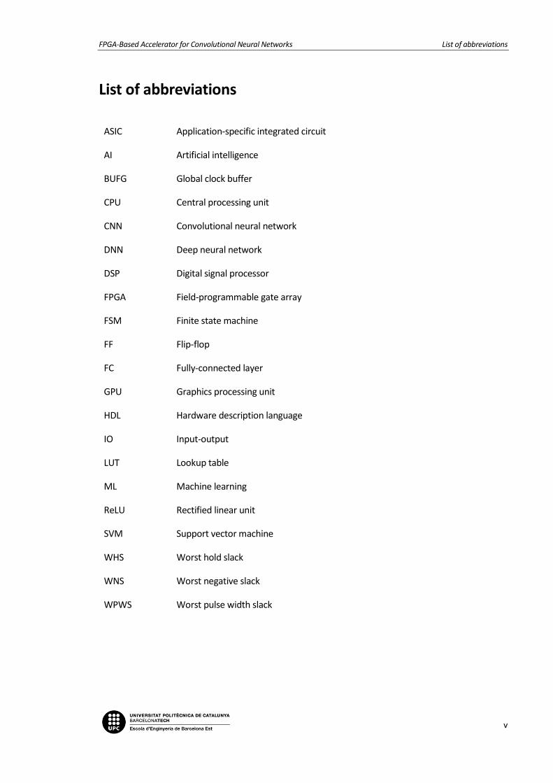
List of abbreviations
ASIC Application-specific integrated circuit
AI Artificial intelligence
BUFG Global clock buffer
CPU Central processing unit
CNN Convolutional neural network
DNN Deep neural network
DSP Digital signal processor
FPGA Field-programmable gate array
FSM Finite state machine
FF Flip-flop
FC Fully-connected layer
GPU Graphics processing unit
HDL Hardware description language
IO Input-output
LUT Lookup table
ML Machine learning
ReLU Rectified linear unit
SVM Support vector machine
WHS Worst hold slack
WNS Worst negative slack
WPWS Worst pulse width slack
FPGA-Based Accelerator for Convolutional Neural Networks List of figures
vi
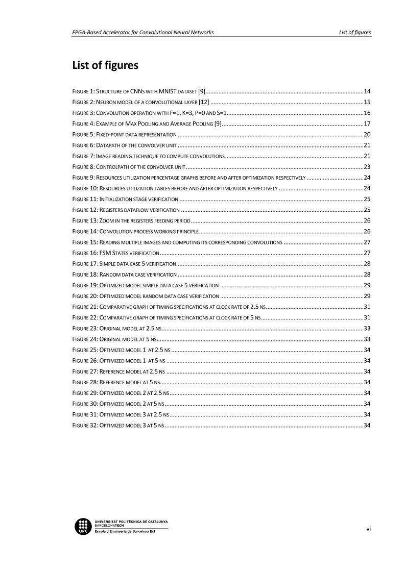
List of figures
FIGURE 1: STRUCTURE OF CNNS WITH MNIST DATASET [9] ................................................................................................. 14
FIGURE 2: NEURON MODEL OF A CONVOLUTIONAL LAYER [12] .............................................................................................. 15
FIGURE 3: CONVOLUTION OPERATION WITH F=1, K=3, P=0 AND S=1 .................................................................................... 16
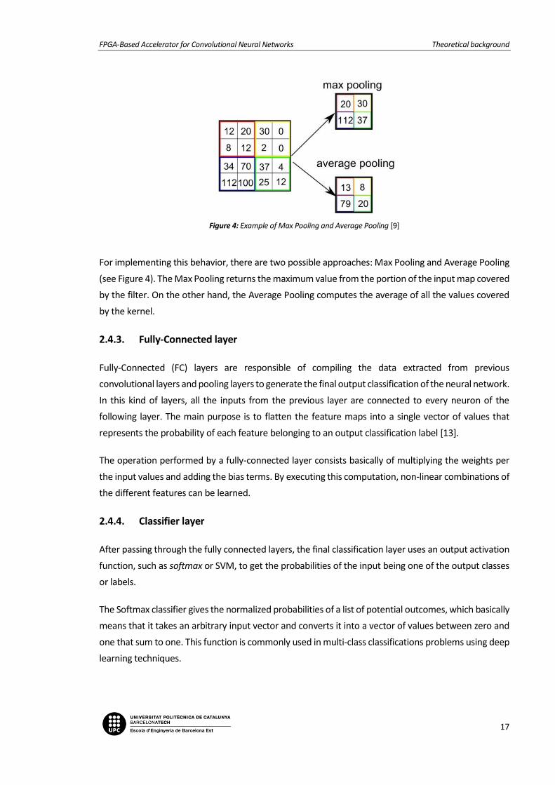
FIGURE 4: EXAMPLE OF MAX POOLING AND AVERAGE POOLING [9] ....................................................................................... 17
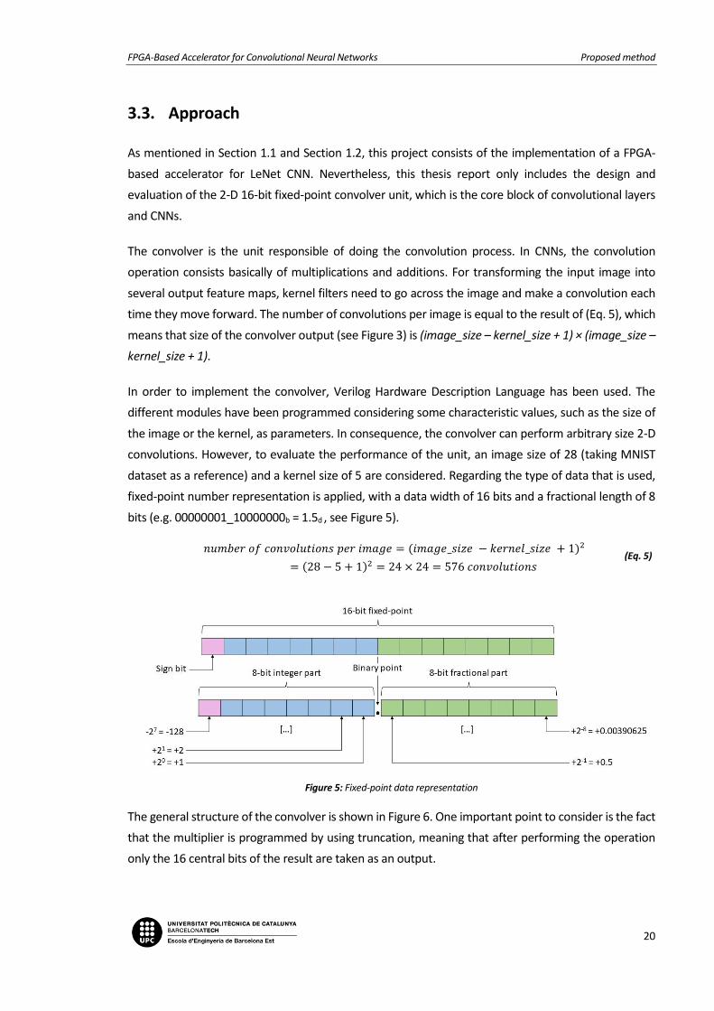
FIGURE 5: FIXED-POINT DATA REPRESENTATION .................................................................................................................. 20
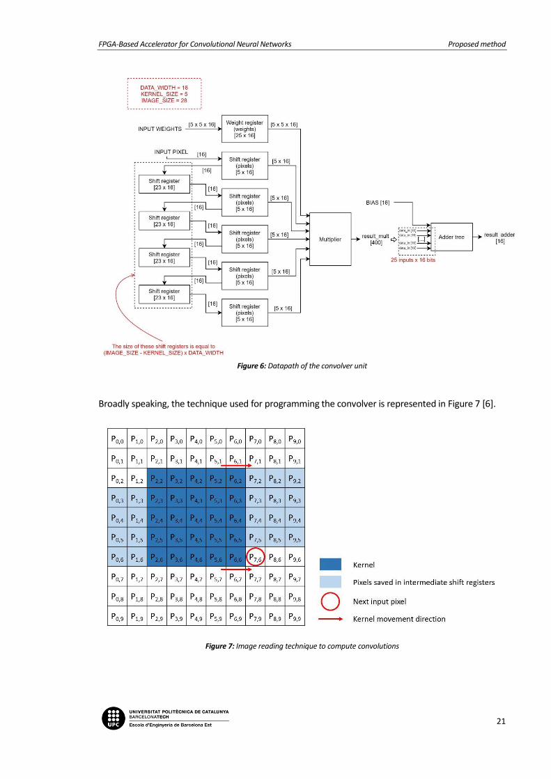
FIGURE 6: DATAPATH OF THE CONVOLVER UNIT .................................................................................................................. 21
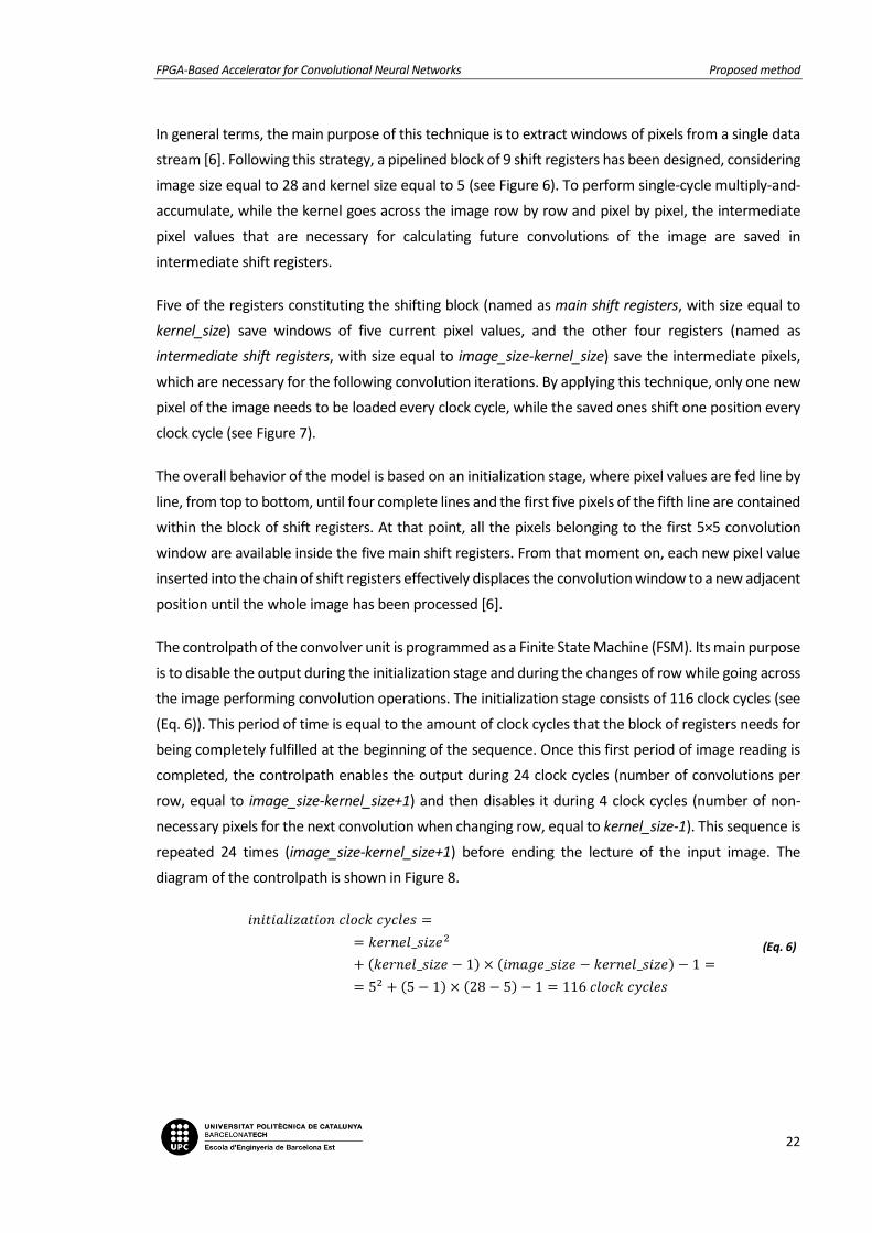
FIGURE 7: IMAGE READING TECHNIQUE TO COMPUTE CONVOLUTIONS ..................................................................................... 21
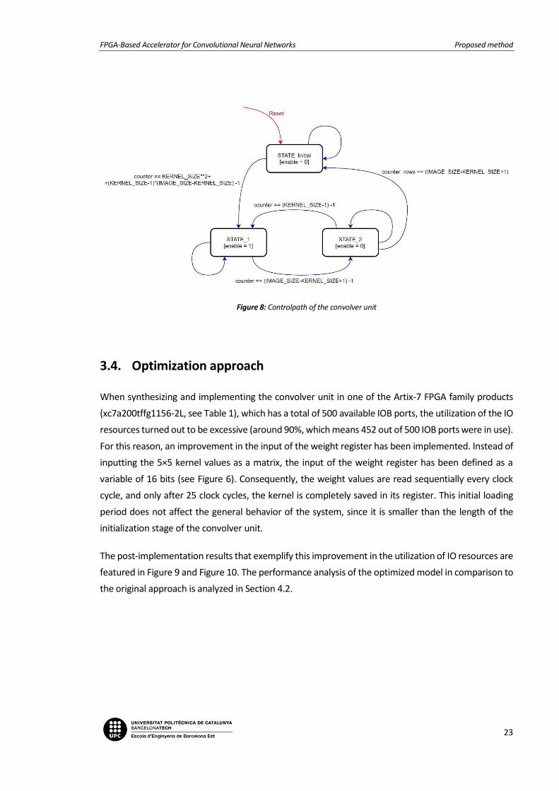
FIGURE 8: CONTROLPATH OF THE CONVOLVER UNIT ............................................................................................................. 23
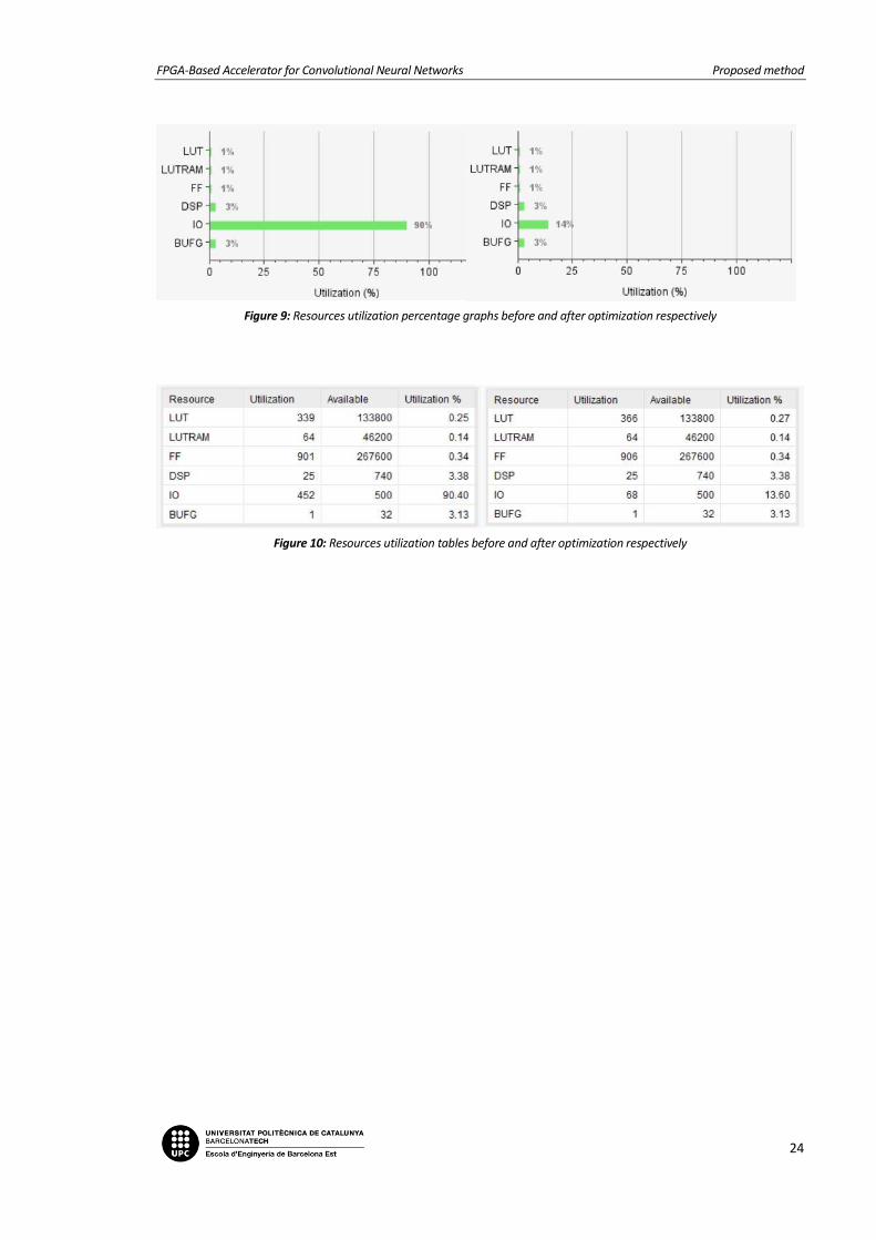
FIGURE 9: RESOURCES UTILIZATION PERCENTAGE GRAPHS BEFORE AND AFTER OPTIMIZATION RESPECTIVELY ................................... 24
FIGURE 10: RESOURCES UTILIZATION TABLES BEFORE AND AFTER OPTIMIZATION RESPECTIVELY .................................................... 24
FIGURE 11: INITIALIZATION STAGE VERIFICATION ................................................................................................................. 25
FIGURE 12: REGISTERS DATAFLOW VERIFICATION ................................................................................................................ 25
FIGURE 13: ZOOM IN THE REGISTERS FEEDING PERIOD .......................................................................................................... 26
FIGURE 14: CONVOLUTION PROCESS WORKING PRINCIPLE ..................................................................................................... 26
FIGURE 15: READING MULTIPLE IMAGES AND COMPUTING ITS CORRESPONDING CONVOLUTIONS ................................................. 27
FIGURE 16: FSM STATES VERIFICATION ............................................................................................................................. 27
FIGURE 17: SIMPLE DATA CASE 5 VERIFICATION ................................................................................................................... 28
FIGURE 18: RANDOM DATA CASE VERIFICATION .................................................................................................................. 28
FIGURE 19: OPTIMIZED MODEL SIMPLE DATA CASE 5 VERIFICATION ........................................................................................ 29
FIGURE 20: OPTIMIZED MODEL RANDOM DATA CASE VERIFICATION ........................................................................................ 29
FIGURE 21: COMPARATIVE GRAPH OF TIMING SPECIFICATIONS AT CLOCK RATE OF 2.5 NS ............................................................ 31
FIGURE 22: COMPARATIVE GRAPH OF TIMING SPECIFICATIONS AT CLOCK RATE OF 5 NS ............................................................... 31
FIGURE 23: ORIGINAL MODEL AT 2.5 NS ............................................................................................................................ 33
FIGURE 24: ORIGINAL MODEL AT 5 NS ............................................................................................................................... 33
FIGURE 25: OPTIMIZED MODEL 1 AT 2.5 NS ...................................................................................................................... 34
FIGURE 26: OPTIMIZED MODEL 1 AT 5 NS ......................................................................................................................... 34
FIGURE 27: REFERENCE MODEL AT 2.5 NS ......................................................................................................................... 34
FIGURE 28: REFERENCE MODEL AT 5 NS............................................................................................................................. 34
FIGURE 29: OPTIMIZED MODEL 2 AT 2.5 NS ....................................................................................................................... 34
FIGURE 30: OPTIMIZED MODEL 2 AT 5 NS .......................................................................................................................... 34
FIGURE 31: OPTIMIZED MODEL 3 AT 2.5 NS ....................................................................................................................... 34
FIGURE 32: OPTIMIZED MODEL 3 AT 5 NS .......................................................................................................................... 34
FPGA-Based Accelerator for Convolutional Neural Networks List of appendix figures
vii
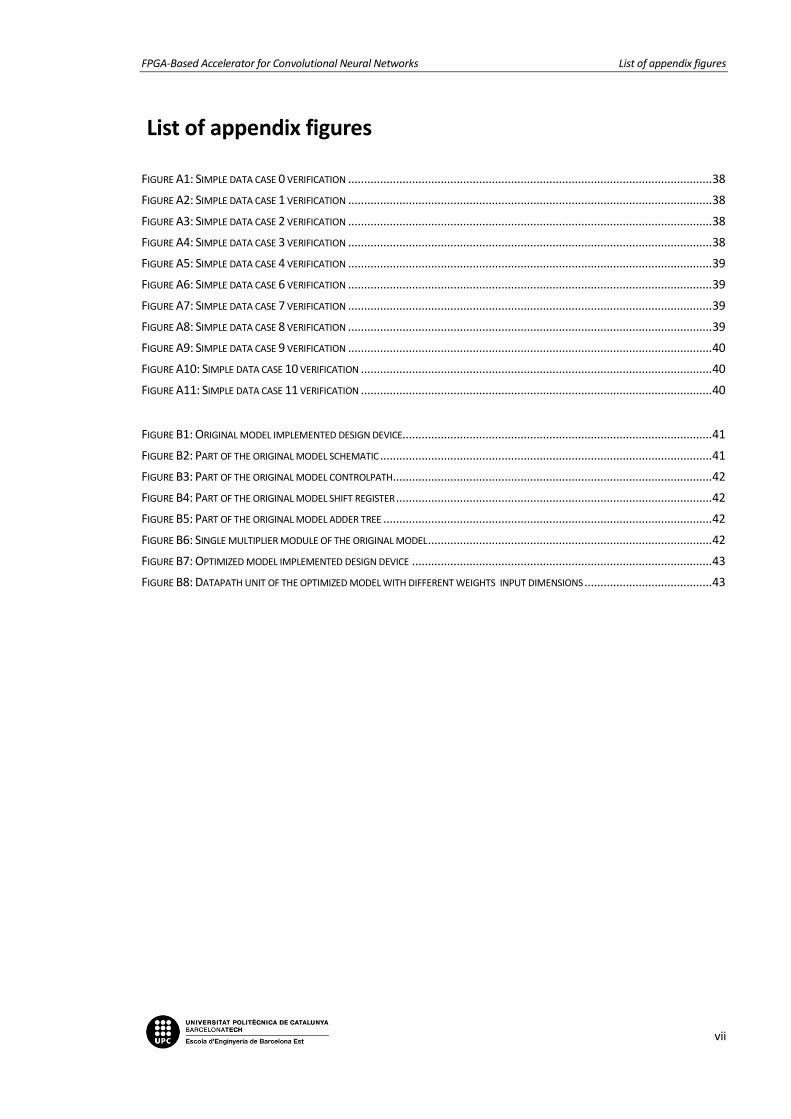
List of appendix figures
FIGURE A1: SIMPLE DATA CASE 0 VERIFICATION .................................................................................................................. 38
FIGURE A2: SIMPLE DATA CASE 1 VERIFICATION .................................................................................................................. 38
FIGURE A3: SIMPLE DATA CASE 2 VERIFICATION .................................................................................................................. 38
FIGURE A4: SIMPLE DATA CASE 3 VERIFICATION .................................................................................................................. 38
FIGURE A5: SIMPLE DATA CASE 4 VERIFICATION .................................................................................................................. 39
FIGURE A6: SIMPLE DATA CASE 6 VERIFICATION .................................................................................................................. 39
FIGURE A7: SIMPLE DATA CASE 7 VERIFICATION .................................................................................................................. 39
FIGURE A8: SIMPLE DATA CASE 8 VERIFICATION .................................................................................................................. 39
FIGURE A9: SIMPLE DATA CASE 9 VERIFICATION .................................................................................................................. 40
FIGURE A10: SIMPLE DATA CASE 10 VERIFICATION .............................................................................................................. 40
FIGURE A11: SIMPLE DATA CASE 11 VERIFICATION .............................................................................................................. 40
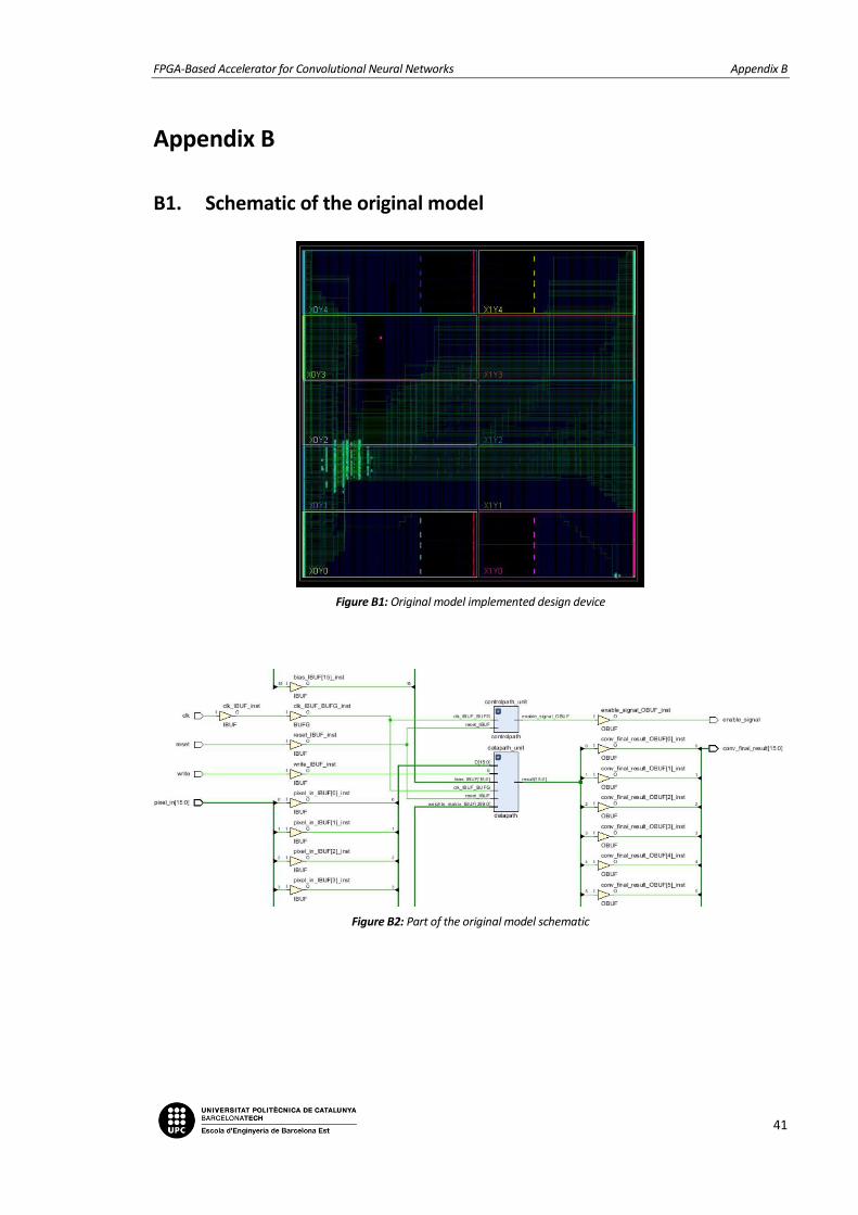
FIGURE B1: ORIGINAL MODEL IMPLEMENTED DESIGN DEVICE................................................................................................. 41
FIGURE B2: PART OF THE ORIGINAL MODEL SCHEMATIC ........................................................................................................ 41
FIGURE B3: PART OF THE ORIGINAL MODEL CONTROLPATH .................................................................................................... 42
FIGURE B4: PART OF THE ORIGINAL MODEL SHIFT REGISTER ................................................................................................... 42
FIGURE B5: PART OF THE ORIGINAL MODEL ADDER TREE ....................................................................................................... 42
FIGURE B6: SINGLE MULTIPLIER MODULE OF THE ORIGINAL MODEL ......................................................................................... 42
FIGURE B7: OPTIMIZED MODEL IMPLEMENTED DESIGN DEVICE .............................................................................................. 43
FIGURE B8: DATAPATH UNIT OF THE OPTIMIZED MODEL WITH DIFFERENT WEIGHTS INPUT DIMENSIONS ........................................ 43
FPGA-Based Accelerator for Convolutional Neural Networks List of tables
viii
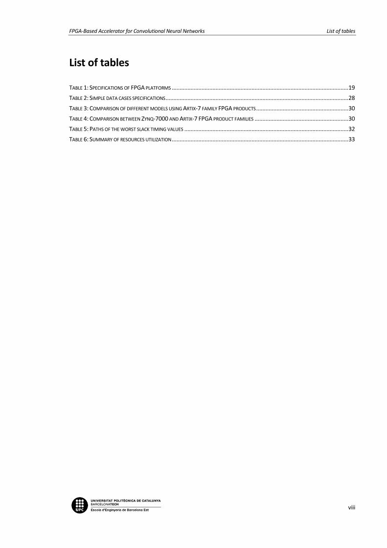
List of tables
TABLE 1: SPECIFICATIONS OF FPGA PLATFORMS ................................................................................................................. 19
TABLE 2: SIMPLE DATA CASES SPECIFICATIONS ..................................................................................................................... 28
TABLE 3: COMPARISON OF DIFFERENT MODELS USING ARTIX-7 FAMILY FPGA PRODUCTS ........................................................... 30
TABLE 4: COMPARISON BETWEEN ZYNQ-7000 AND ARTIX-7 FPGA PRODUCT FAMILIES ............................................................ 30
TABLE 5: PATHS OF THE WORST SLACK TIMING VALUES ......................................................................................................... 32
TABLE 6: SUMMARY OF RESOURCES UTILIZATION ................................................................................................................. 33
FPGA-Based Accelerator for Convolutional Neural Networks List of tables
ix
Table of contents
ABSTRACT ___________________________________________________________ I
RESUM _____________________________________________________________ II
RESUMEN __________________________________________________________ III
ACKNOWLEDGMENTS _________________________________________________ IV
LIST OF ABBREVIATIONS _______________________________________________ V
LIST OF FIGURES _____________________________________________________ VI
LIST OF APPENDIX FIGURES ___________________________________________ VII
LIST OF TABLES _____________________________________________________ VIII
1. INTRODUCTION ________________________________________________ 11
1.1. Motivation .............................................................................................................. 11
1.2. Thesis scope ........................................................................................................... 12
2. THEORETICAL BACKGROUND _____________________________________ 13
2.1. Artificial Intelligence and Machine Learning ......................................................... 13
2.2. Convolutional Neural Networks ............................................................................ 13
2.3. LeNet CNN .............................................................................................................. 14
2.4. Structure of LeNet CNN ......................................................................................... 15
2.4.1. Convolutional layer ............................................................................................... 15
2.4.2. Pooling layer ......................................................................................................... 16
2.4.3. Fully-Connected layer ........................................................................................... 17
2.4.4. Classifier layer ....................................................................................................... 17
2.4.5. Activation function ............................................................................................... 18
3. PROPOSED METHOD ____________________________________________ 19
3.1. Tools ....................................................................................................................... 19
3.2. FPGA platforms ...................................................................................................... 19
3.3. Approach ................................................................................................................ 20
3.4. Optimization approach .......................................................................................... 23
4. EXPERIMENTAL SETUP ___________________________________________ 25
4.1. Timing and behavior simulations ........................................................................... 25
FPGA-Based Accelerator for Convolutional Neural Networks List of tables
x
4.2. Performance analysis ............................................................................................. 29
CONCLUSIONS AND RECOMMENDATIONS _______________________________ 35
REFERENCES _______________________________________________________ 36
APPENDIX A ________________________________________________________ 38
A1. Verification of simple cases behavioral simulations ............................................. 38
APPENDIX B ________________________________________________________ 41
B1. Schematic of the original model ............................................................................ 41
B2. Schematic of the optimized model ........................................................................ 43
FPGA-Based Accelerator for Convolutional Neural Networks Introduction
11
1. Introduction
During the last decade, Convolutional Neural Networks (CNNs) have suffered an exponential growth in
terms of data computation and applicability. CNNs are a class of deep neural network (DNN), which
use convolution instead of general matrix multiplication in at least one of their layers. Nowadays, CNNs
are used in a wide range of fields, such as image analysis, facial and speech recognition, medical
diagnosis, and computer vision, in which object detection, classification, and segmentation have the
strongest impact. However, this rapid expansion of CNNs creates additional requirements regarding
memory footprint and power consumption, and therefore challenges the latency and accuracy of the
network and limits its complexity in terms of number of layers and parameters [1]. For this reason,
FPGA-based hardware accelerators for CNNs provide a flexible and cost-efficient solution for dealing
with these limitations.
In order to boost the performance of CNNs, field-programmable devices (FPGAs) are a promising
platform for low power hardware acceleration thanks to its high energy and resource efficiency,
computing capabilities, and reconfigurability [2]. When comparing FPGA to other conventional tools,
CPUs and GPUs offer a lower throughput and less energy efficiency. FPGAs are easy and fast to develop,
and they offer high flexibility, configurability, and diversity. In contrast, ASIC requires elaborate
customization and high fabrication investments and leads to a lack of reconfigurability [3].
Although FPGAs present a large number of advantages and a remarkable performance with CNNs,
limited bandwidth and on-chip memory requirements can be crucial problems to consider when
designing a CNN accelerator [4]. CNNs are constantly improving and becoming deeper, more complex,
and more computationally intensive. Consequently, the dimension of data, as well as the memory
footprint, becomes higher.
The aim of this project is to design a hardware accelerator, which presents good energy-efficiency and
high-speed results, for LeNet CNN on FPGA using Vivado Design Tool.
1.1. Motivation
As mentioned in the previous section, CNNs have achieved very accurate results in various application
areas. The improvements in this type of neural networks are arising at a rapid pace. More powerful
hardware, larger datasets, bigger models, new algorithms and improved network architectures are
constantly challenging the state-of-the-art of CNNs [5].
The main idea of this thesis is to achieve a wider knowledge of the world of design and evaluation of
efficient deep neural network architectures. With the objective of reducing the computational cost in
FPGA-Based Accelerator for Convolutional Neural Networks Introduction
12
terms of time performance and power consumption, this project proposes a FPGA-based accelerator
for CNNs. More precisely, the work presented in this report is focused on the development of a two-
dimensional hardware convolver, which will constitute the core block of the FPGA-based accelerator.
1.2. Thesis scope
This thesis report proposes the implementation of a 2-D convolver, which is able to compute arbitrary-
size 2-D convolutions. Two-dimensional convolutions are an extremely demanding mathematical
operation in terms of real-time system performance. Indeed, they require more than 300 million
multiplications and additions per second [6].
In order to implement this 2-D convolver with the capability of single-cycle multiply-and-accumulate,
a strategy to extract windows of pixels from a single data stream has been adopted. This applied
method will be described in detail in Section 3.3. The main boundary of this approach could be memory
requirements. The number of registers needed to store all the intermediate values required for the
operation may be very expensive regarding memory footprint.
Every module in this design is obtained through the synthesis of Verilog behavioral descriptions. In
terms of implementation, the Vivado design environment provides all the compilation, simulation, and
synthesis tools required for developing the tasks of this thesis. More precisely, this project explores the
performance involved in the design of the 2-D convolver for Xilinx FPGA devices from different product
families, such as Artix-7 or Zynq-7000 (see Section 3.2).
The main goal of this thesis was the design, evaluation and implementation of a FPGA-based
accelerator for LeNet CNN. Nevertheless, due to time constraints, this report is limited to the design
and evaluation of the core block of LeNet CNN, which consists of the 2-D convolver unit.
The project outline is featured below.
• Section 2: The theoretical background of Machine Learning, CNNs and especially LeNet CNN is
described in detail.
• Section 3: This chapter defines the tools, design approaches and evaluation criteria used in the
project.
• Section 4: The results of the thesis are stated regarding timing, behavior and performance
evaluation.
FPGA-Based Accelerator for Convolutional Neural Networks Theoretical background
13
2. Theoretical background
2.1. Artificial Intelligence and Machine Learning
Artificial Intelligence (AI) is the science of training machines to perform human tasks. Some decades
ago, this term first appeared when scientists looked for a way of making computers capable of solving
problems on their own. Intelligent machines that can emulate human behavior became a powerful and
promising tool. The ability of independent reasoning and self-decision making led to the exponential
growth of this new concept.
As this new scientific term started to play an important role in the engineering field, the idea of learning
from actual actions to improve future results came to light, bringing up the concept of machine
learning. Machine learning is a specific subset of AI that trains a machine on how to learn from data
and make predictions [7]. Despite its initial implication with pattern recognition, machine learning is
nowadays employed in a wide range of applications related to computer systems, such as classification,
computer vision, and medicine. This groundbreaking method consists of looking for patterns and
drawing conclusions without being explicitly programmed, only based on previous examples
(datasets). Learning algorithms and complex models have been developed through learning from
historical relationships and trends in data, generating in consequence reliable decisions and high
accuracy results.
Inspired by the workings of the human brain, neural networks are a computing system approach inside
the machine learning field that tries to mimic how the human brain learns. It incorporates
interconnected units (like neurons) that process information by responding to external inputs,
transferring it between each unit multiple times to set optimal connections and parameters that can
later extract conclusions from undefined data.
2.2. Convolutional Neural Networks
In machine learning, a CNN is a type of neural network that consists of millions of neurons with
learnable weights and biases, which are organized in several layers. CNNs are inspired by biological
processes and its structure is equivalent to the connectivity pattern of neurons in the human brain.
They differ from conventional neural networks because of performing convolution instead of standard
matrix multiplication [8].
The preprocessing stage required in a CNN is minimum in comparison to other traditional image
classification algorithms. With optimal training, this type of network has the ability of learning the
values of the filters and other parameters on its own through backpropagation.
FPGA-Based Accelerator for Convolutional Neural Networks Theoretical background
14
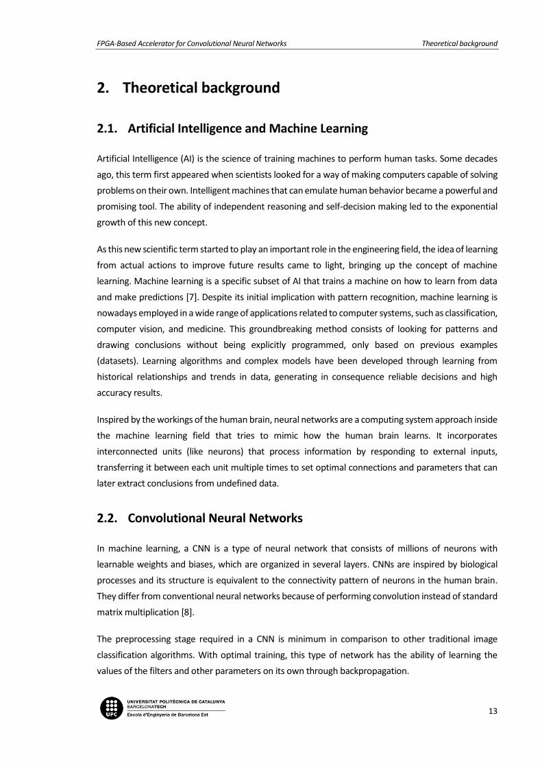
The architecture of CNNs is composed of an initial convolution layer, multiple hidden layers, several
fully-connected layers, and a final fully-connected layer, called the classifier (see Figure 1). The main
purpose of the first convolution layer is to extract features from the input image and drive them into
the hidden layers, which are pooling layers and convolution layers partially connected. Between hidden
layers, there are normally activation functions that help to keep important information for the next
layers. The last fully-connected layer has a loss function, such as softmax or SVM, that allows the
classification at the end.
Figure 1: Structure of CNNs with MNIST dataset [9]
This kind of neural network is popular for two distinct attributes: sparse interactions and parameter
sharing [8]. Making the kernel filter size smaller than the size of the input image allows capturing only
important features and turning them into different feature maps that are driven through the different
layers of the CNN. With fewer pixels of the image in consideration, sparse interactions or connectivity,
as well as a reduction in parameters, is achieved. In consequence, this results in the reduction of
memory footprint and computational overfitting.
CNNs are commonly applied in the analysis of visual data. They are an effective solution for image
recognition and classification.
2.3. LeNet CNN
LeNet is one of the first CNNs, developed by Yann LeCun in the 1990s [8]. In the beginning, it was mainly
used for character recognition applications, like reading zip codes or digits. The LeNet architecture is
considered simple and small regarding memory footprint, although it is efficient enough to provide
FPGA-Based Accelerator for Convolutional Neural Networks Theoretical background
15
good results in many fields. The latest approach is called LeNet-5, which is a 5-layer CNN that reaches
99.2% accuracy on isolated character recognition [10].
As many CNNs (see Figure 1), the structure of LeNet combines two sets of convolutional layers and
pooling layers, followed by fully-connected layers and finally a softmax classifier [11]. Commonly, the
non-linear ReLU function is applied at the output of some of the nodes, acting as the activation function
of the neuron (see Section 2.4.5).
2.4. Structure of LeNet CNN
A detailed description of the different layers that constitute the LeNet CNN is featured below.
2.4.1. Convolutional layer
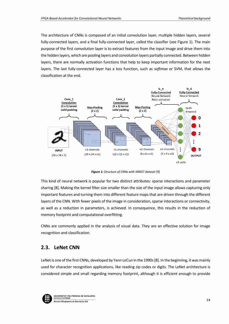
Convolutional layers are the core block of CNNs. This kind of layers apply a convolution operation
across the width and height of the input image, generating feature maps as an output. For each input
position, a dot product between the learnable filter and the corresponding pixels is computed.
Figure 2: Neuron model of a convolutional layer [12]
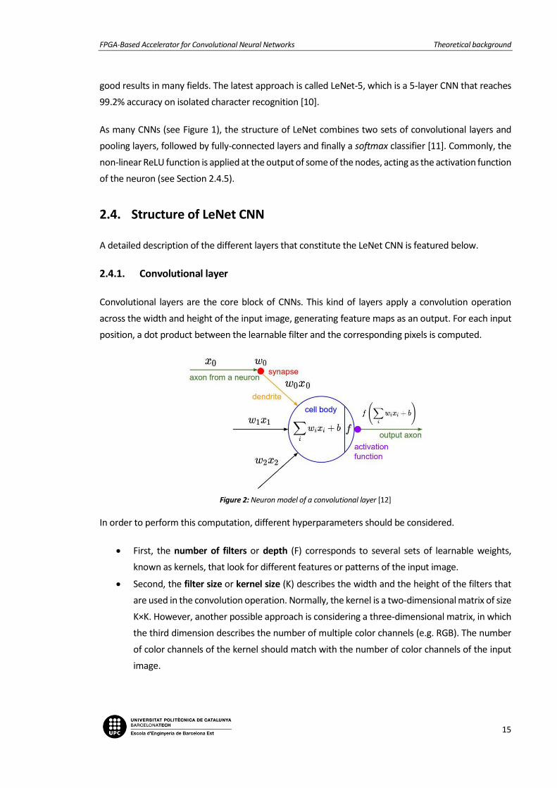
In order to perform this computation, different hyperparameters should be considered.
• First, the number of filters or depth (F) corresponds to several sets of learnable weights,
known as kernels, that look for different features or patterns of the input image.
• Second, the filter size or kernel size (K) describes the width and the height of the filters that
are used in the convolution operation. Normally, the kernel is a two-dimensional matrix of size
K×K. However, another possible approach is considering a three-dimensional matrix, in which
the third dimension describes the number of multiple color channels (e.g. RGB). The number
of color channels of the kernel should match with the number of color channels of the input
image.
FPGA-Based Accelerator for Convolutional Neural Networks Theoretical background
16
• Third, the zero-padding (P) defines how the convolution operation is performed, based on
which the generated output size changes. Depending on this hyperparameter, the input is
padded or not with zeros around the border.
• Finally, the stride (S) corresponds to the number of positions that the filter is slid each time.
This value can also produce a variation on the output size.
Figure 3: Convolution operation with F=1, K=3, P=0 and S=1
Taking all these definitions into account, the number of trainable parameters (TP) is defined as:
𝑇𝑃 = 𝑤𝑒𝑖𝑔ℎ𝑡𝑠 + 𝑏𝑖𝑎𝑠𝑒𝑠 = 𝐾2 × 𝐹 + 𝐹 (Eq. 1)
The number of connections (NC) is given by:
𝑁𝐶 = 𝑜𝑢𝑡𝑝𝑢𝑡_𝑠𝑖𝑧𝑒2 × 𝑇𝑃 (Eq. 2)
in which the output size corresponds to:
𝑜𝑢𝑡𝑝𝑢𝑡_𝑠𝑖𝑧𝑒 = 𝑖𝑛𝑝𝑢𝑡_𝑠𝑖𝑧𝑒 − 𝐾 + 1 (Eq. 3)
2.4.2. Pooling layer
The pooling layer or sub-sampling layer is commonly placed between convolutional layers with the
objective of reducing the number of trainable parameters and computation in the neural network. In
order to achieve a better power performance, this kind of layer reduces the spatial size of the input
feature maps. By performing this size reduction, it also helps avoiding overfitting in the CNN. Normally,
it operates with filters of size 2x2 and a stride of 2.
FPGA-Based Accelerator for Convolutional Neural Networks Theoretical background
17
Figure 4: Example of Max Pooling and Average Pooling [9]
For implementing this behavior, there are two possible approaches: Max Pooling and Average Pooling
(see Figure 4). The Max Pooling returns the maximum value from the portion of the input map covered
by the filter. On the other hand, the Average Pooling computes the average of all the values covered
by the kernel.
2.4.3. Fully-Connected layer
Fully-Connected (FC) layers are responsible of compiling the data extracted from previous
convolutional layers and pooling layers to generate the final output classification of the neural network.
In this kind of layers, all the inputs from the previous layer are connected to every neuron of the
following layer. The main purpose is to flatten the feature maps into a single vector of values that
represents the probability of each feature belonging to an output classification label [13].
The operation performed by a fully-connected layer consists basically of multiplying the weights per
the input values and adding the bias terms. By executing this computation, non-linear combinations of
the different features can be learned.
2.4.4. Classifier layer
After passing through the fully connected layers, the final classification layer uses an output activation
function, such as softmax or SVM, to get the probabilities of the input being one of the output classes
or labels.
The Softmax classifier gives the normalized probabilities of a list of potential outcomes, which basically
means that it takes an arbitrary input vector and converts it into a vector of values between zero and
one that sum to one. This function is commonly used in multi-class classifications problems using deep
learning techniques.
FPGA-Based Accelerator for Convolutional Neural Networks Theoretical background
18
The SVM (Support Vector Machines) classifier is applied for finding a hyperplane in a N-dimensional
space (where N is equal to the number of features) that distinctly classifies the different data points of
each class or label [14].
2.4.5. Activation function
In neural networks, the activation function of a node defines the output of that node given an input or
set of inputs (see Figure 2) [7]. More precisely, it produces a mapping from an input real number to a
real number within a specific range in order to determine whether or not the information within the
node is useful [8].
In consequence, given a combination of inputs and weights from the previous layer, the activation
function controls how the information is processed and passed to the next layer. These mathematical
equations are crucial when talking about the accuracy, computational efficiency, convergence and
convergence speed of a model.
An ideal activation function is both nonlinear and differentiable. Nonlinear behavior of an activation
function allows our neural network to learn nonlinear relationships in the data. Differentiability is
important because it allows to backpropagate the error in the neural network model when training to
optimize the weights.
Apart from the softmax output activation function described in Section 2.4.4, the ReLU (rectified linear
unit) is one of the most popular activation functions [15], especially in CNNs. Non-linear activation
functions help the network learn complex data and provide accurate predictions. Mathematically,
ReLU is defined as:
𝑦 = max (0, 𝑥) (Eq. 4)
This function is cheap to compute, trains rapidly, converges fast and is sparsely activated. Neurons in
a network have different roles and therefore should be activated by different signals. Being sparsely
activated allows neurons to process meaningful aspects of the problem. Nowadays, there are several
variants of the ReLU activation function.
Although there are other activation functions, such as perceptron or sigmoid (tanh or arctan), those
functions are not used nowadays because of their non-differentiability or their backpropagation
limitations respectively.
FPGA-Based Accelerator for Convolutional Neural Networks Proposed method
19
3. Proposed method
3.1. Tools
Xilinx Vivado Design Suite – HLx Editions Version 2018.2 is the tool that has been used to implement
the design proposed in this project. Vivado Design Suite is a software developed by Xilinx that allows
the synthesis and analysis of HDL designs, both in VHDL and Verilog. In this case, the hardware
description language used for modelling the unit is Verilog.
Vivado design environment has provided the necessary resources for synthesizing and implementing
the design of the 2-D convolver block. Additionally, this tool presents the option of exporting
implementation reports showing the performance of the generated design in terms of timing,
utilization and power.
For performing the timing and behavior simulations of the model, Vivado software and ModelSim
software have been used.
3.2. FPGA platforms
The designed architecture of the 2-D convolver unit has been implemented in two Xilinx FPGA families
by using the Vivado software. The platforms in which the performance of model has been analyzed are
from Artix-7 and Zynq-7000 families [16] [17]. The description of the tested FPGA devices from both
families is shown in Table 1.
Table 1: Specifications of FPGA platforms
FPGA platform Product family
Available resources
LUT LUTRAM FF DSP IO BUFG
xc7a200tffg1156-2L Artix-7 133800 46200 267600 740 500 32
xc7a25tcsg325-2L Artix-7 14600 5000 29200 80 150 32
xc7z030isbg485-2L Zynq-7000 78600 26600 157200 400 150 32
In the Vivado Design Tool, the Zynq-7000 family has license limitations. In consequence, the analysis of
a model using platforms with a big amount of IO ports (more precisely, more than 250 IOs) is not
available.
An important highlight of the utilization of FPGA devices that integrate 150 IO ports is the fact that they
fit better with the design needs of the optimized model of the convolver unit.
FPGA-Based Accelerator for Convolutional Neural Networks Proposed method
20
3.3. Approach
As mentioned in Section 1.1 and Section 1.2, this project consists of the implementation of a FPGA-
based accelerator for LeNet CNN. Nevertheless, this thesis report only includes the design and
evaluation of the 2-D 16-bit fixed-point convolver unit, which is the core block of convolutional layers
and CNNs.
The convolver is the unit responsible of doing the convolution process. In CNNs, the convolution
operation consists basically of multiplications and additions. For transforming the input image into
several output feature maps, kernel filters need to go across the image and make a convolution each
time they move forward. The number of convolutions per image is equal to the result of (Eq. 5), which
means that size of the convolver output (see Figure 3) is (image_size – kernel_size + 1) × (image_size –
kernel_size + 1).
In order to implement the convolver, Verilog Hardware Description Language has been used. The
different modules have been programmed considering some characteristic values, such as the size of
the image or the kernel, as parameters. In consequence, the convolver can perform arbitrary size 2-D
convolutions. However, to evaluate the performance of the unit, an image size of 28 (taking MNIST
dataset as a reference) and a kernel size of 5 are considered. Regarding the type of data that is used,
fixed-point number representation is applied, with a data width of 16 bits and a fractional length of 8
bits (e.g. 00000001_10000000b = 1.5d , see Figure 5).
𝑛𝑢𝑚𝑏𝑒𝑟 𝑜𝑓 𝑐𝑜𝑛𝑣𝑜𝑙𝑢𝑡𝑖𝑜𝑛𝑠 𝑝𝑒𝑟 𝑖𝑚𝑎𝑔𝑒 = (𝑖𝑚𝑎𝑔𝑒_𝑠𝑖𝑧𝑒 − 𝑘𝑒𝑟𝑛𝑒𝑙_𝑠𝑖𝑧𝑒 + 1)2
= (28 − 5 + 1)2 = 24 × 24 = 576 𝑐𝑜𝑛𝑣𝑜𝑙𝑢𝑡𝑖𝑜𝑛𝑠 (Eq. 5)
Figure 5: Fixed-point data representation
The general structure of the convolver is shown in Figure 6. One important point to consider is the fact
that the multiplier is programmed by using truncation, meaning that after performing the operation
only the 16 central bits of the result are taken as an output.
FPGA-Based Accelerator for Convolutional Neural Networks Proposed method
21
Figure 6: Datapath of the convolver unit
Broadly speaking, the technique used for programming the convolver is represented in Figure 7 [6].
Figure 7: Image reading technique to compute convolutions
FPGA-Based Accelerator for Convolutional Neural Networks Proposed method
22
In general terms, the main purpose of this technique is to extract windows of pixels from a single data
stream [6]. Following this strategy, a pipelined block of 9 shift registers has been designed, considering
image size equal to 28 and kernel size equal to 5 (see Figure 6). To perform single-cycle multiply-and-
accumulate, while the kernel goes across the image row by row and pixel by pixel, the intermediate
pixel values that are necessary for calculating future convolutions of the image are saved in
intermediate shift registers.
Five of the registers constituting the shifting block (named as main shift registers, with size equal to
kernel_size) save windows of five current pixel values, and the other four registers (named as
intermediate shift registers, with size equal to image_size-kernel_size) save the intermediate pixels,
which are necessary for the following convolution iterations. By applying this technique, only one new
pixel of the image needs to be loaded every clock cycle, while the saved ones shift one position every
clock cycle (see Figure 7).
The overall behavior of the model is based on an initialization stage, where pixel values are fed line by
line, from top to bottom, until four complete lines and the first five pixels of the fifth line are contained
within the block of shift registers. At that point, all the pixels belonging to the first 5×5 convolution
window are available inside the five main shift registers. From that moment on, each new pixel value
inserted into the chain of shift registers effectively displaces the convolution window to a new adjacent
position until the whole image has been processed [6].
The controlpath of the convolver unit is programmed as a Finite State Machine (FSM). Its main purpose
is to disable the output during the initialization stage and during the changes of row while going across
the image performing convolution operations. The initialization stage consists of 116 clock cycles (see
(Eq. 6)). This period of time is equal to the amount of clock cycles that the block of registers needs for
being completely fulfilled at the beginning of the sequence. Once this first period of image reading is
completed, the controlpath enables the output during 24 clock cycles (number of convolutions per
row, equal to image_size-kernel_size+1) and then disables it during 4 clock cycles (number of non-
necessary pixels for the next convolution when changing row, equal to kernel_size-1). This sequence is
repeated 24 times (image_size-kernel_size+1) before ending the lecture of the input image. The
diagram of the controlpath is shown in Figure 8.
𝑖𝑛𝑖𝑡𝑖𝑎𝑙𝑖𝑧𝑎𝑡𝑖𝑜𝑛 𝑐𝑙𝑜𝑐𝑘 𝑐𝑦𝑐𝑙𝑒𝑠 =
= 𝑘𝑒𝑟𝑛𝑒𝑙_𝑠𝑖𝑧𝑒2
+ (𝑘𝑒𝑟𝑛𝑒𝑙_𝑠𝑖𝑧𝑒 − 1) × (𝑖𝑚𝑎𝑔𝑒_𝑠𝑖𝑧𝑒 − 𝑘𝑒𝑟𝑛𝑒𝑙_𝑠𝑖𝑧𝑒) − 1 =
= 52 + (5 − 1) × (28 − 5) − 1 = 116 𝑐𝑙𝑜𝑐𝑘 𝑐𝑦𝑐𝑙𝑒𝑠
(Eq. 6)
FPGA-Based Accelerator for Convolutional Neural Networks Proposed method
23
Figure 8: Controlpath of the convolver unit
3.4. Optimization approach
When synthesizing and implementing the convolver unit in one of the Artix-7 FPGA family products
(xc7a200tffg1156-2L, see Table 1), which has a total of 500 available IOB ports, the utilization of the IO
resources turned out to be excessive (around 90%, which means 452 out of 500 IOB ports were in use).
For this reason, an improvement in the input of the weight register has been implemented. Instead of
inputting the 5×5 kernel values as a matrix, the input of the weight register has been defined as a
variable of 16 bits (see Figure 6). Consequently, the weight values are read sequentially every clock
cycle, and only after 25 clock cycles, the kernel is completely saved in its register. This initial loading
period does not affect the general behavior of the system, since it is smaller than the length of the
initialization stage of the convolver unit.
The post-implementation results that exemplify this improvement in the utilization of IO resources are
featured in Figure 9 and Figure 10. The performance analysis of the optimized model in comparison to
the original approach is analyzed in Section 4.2.
FPGA-Based Accelerator for Convolutional Neural Networks Proposed method
24
Figure 9: Resources utilization percentage graphs before and after optimization respectively
Figure 10: Resources utilization tables before and after optimization respectively
FPGA-Based Accelerator for Convolutional Neural Networks Experimental setup
25
4. Experimental setup
4.1. Timing and behavior simulations
In order to verify the operation principle and the correct behavior of the two-dimensional 16-bit fixed
convolver, a number of simulations have been carried out using ModelSim software. The simulations
results are reported in 16-bit fixed-point representation (with 8-bit fractional length), except for the
weights values that are represented in hexadecimal due to data length limitations.
The first step is the verification of the initialization period. Considering a clock speed of 20 ns (50 MHz),
the number of clock cycles during the initialization stage should be equal to 116 (see Section 3.3).
𝑖𝑛𝑖𝑡𝑖𝑎𝑙𝑖𝑧𝑎𝑡𝑖𝑜𝑛 𝑡𝑖𝑚𝑒 = 𝑛𝑢𝑚𝑏𝑒𝑟 𝑜𝑓 𝑐𝑙𝑜𝑐𝑘 𝑐𝑦𝑐𝑙𝑒𝑠 × 𝑐𝑙𝑜𝑐𝑘 𝑝𝑒𝑟𝑖𝑜𝑑 +𝑐𝑙𝑜𝑐𝑘 𝑝𝑒𝑟𝑖𝑜𝑑
2
= 116 × 20 + 10 = 2330 𝑛𝑠
(Eq. 7)
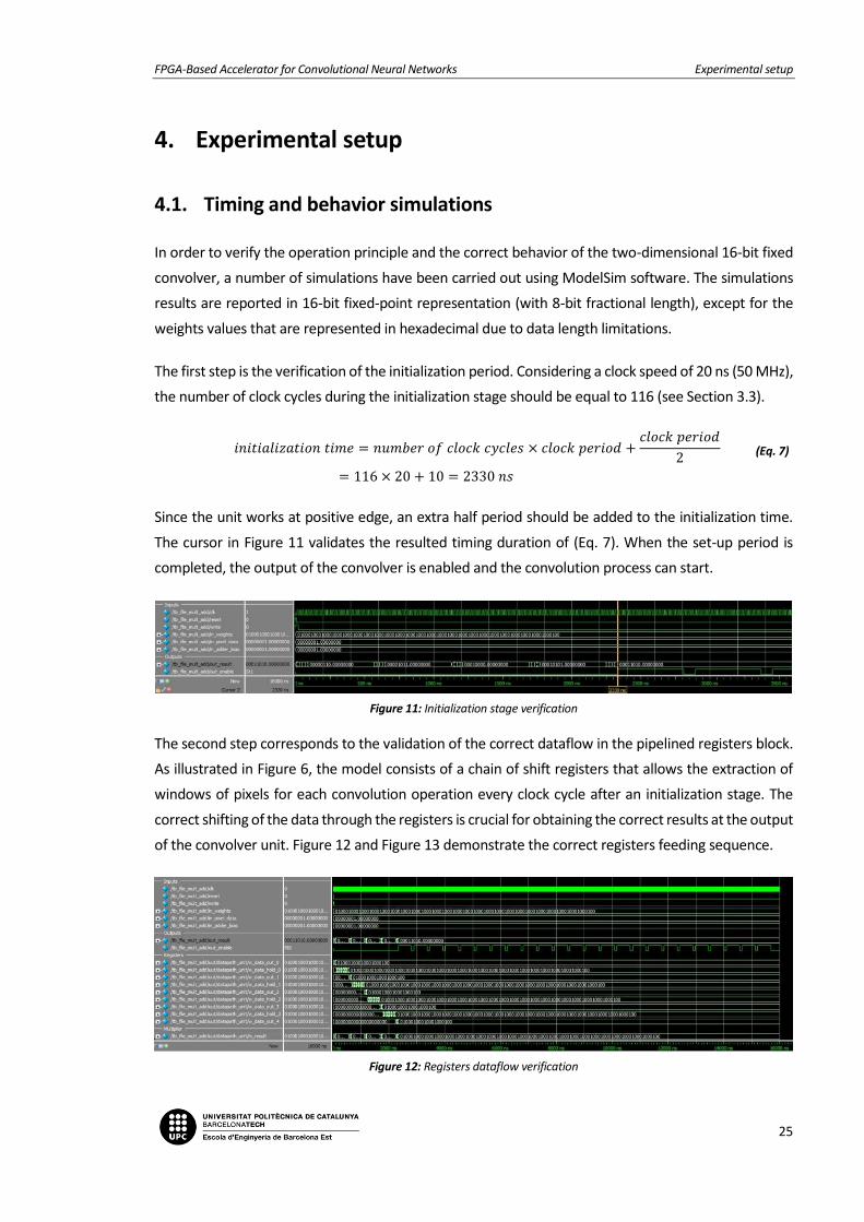
Since the unit works at positive edge, an extra half period should be added to the initialization time.
The cursor in Figure 11 validates the resulted timing duration of (Eq. 7). When the set-up period is
completed, the output of the convolver is enabled and the convolution process can start.
Figure 11: Initialization stage verification
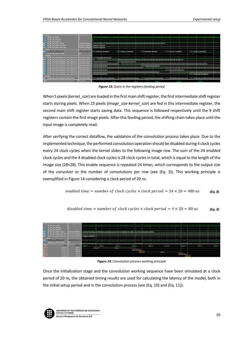
The second step corresponds to the validation of the correct dataflow in the pipelined registers block.
As illustrated in Figure 6, the model consists of a chain of shift registers that allows the extraction of
windows of pixels for each convolution operation every clock cycle after an initialization stage. The
correct shifting of the data through the registers is crucial for obtaining the correct results at the output
of the convolver unit. Figure 12 and Figure 13 demonstrate the correct registers feeding sequence.
Figure 12: Registers dataflow verification
FPGA-Based Accelerator for Convolutional Neural Networks Experimental setup
26
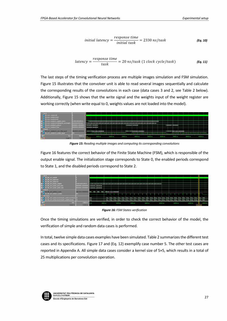
Figure 13: Zoom in the registers feeding period
When 5 pixels (kernel_size) are loaded in the first main shift register, the first intermediate shift register
starts storing pixels. When 23 pixels (image_size-kernel_size) are fed in this intermediate register, the
second main shift register starts saving data. This sequence is followed respectively until the 9 shift
registers contain the first image pixels. After this feeding period, the shifting chain takes place until the
input image is completely read.
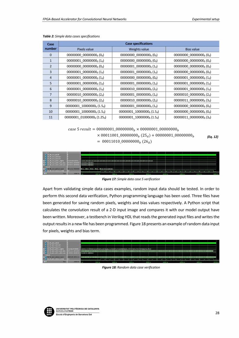
After verifying the correct dataflow, the validation of the convolution process takes place. Due to the
implemented technique, the performed convolution operation should be disabled during 4 clock cycles
every 24 clock cycles when the kernel slides to the following image row. The sum of the 24 enabled
clock cycles and the 4 disabled clock cycles is 28 clock cycles in total, which is equal to the length of the
image size (28×28). This enable sequence is repeated 24 times, which corresponds to the output size
of the convolver or the number of convolutions per row (see (Eq. 3)). This working principle is
exemplified in Figure 14 considering a clock period of 20 ns.
𝑒𝑛𝑎𝑏𝑙𝑒𝑑 𝑡𝑖𝑚𝑒 = 𝑛𝑢𝑚𝑏𝑒𝑟 𝑜𝑓 𝑐𝑙𝑜𝑐𝑘 𝑐𝑦𝑐𝑙𝑒𝑠 × 𝑐𝑙𝑜𝑐𝑘 𝑝𝑒𝑟𝑖𝑜𝑑 = 24 × 20 = 480 𝑛𝑠 (Eq. 8)
𝑑𝑖𝑠𝑎𝑏𝑙𝑒𝑑 𝑡𝑖𝑚𝑒 = 𝑛𝑢𝑚𝑏𝑒𝑟 𝑜𝑓 𝑐𝑙𝑜𝑐𝑘 𝑐𝑦𝑐𝑙𝑒𝑠 × 𝑐𝑙𝑜𝑐𝑘 𝑝𝑒𝑟𝑖𝑜𝑑 = 4 × 20 = 80 𝑛𝑠 (Eq. 9)
Figure 14: Convolution process working principle
Once the initialization stage and the convolution working sequence have been simulated at a clock
period of 20 ns, the obtained timing results are used for calculating the latency of the model, both in
the initial setup period and in the convolution process (see (Eq. 10) and (Eq. 11)).
FPGA-Based Accelerator for Convolutional Neural Networks Experimental setup
27
𝑖𝑛𝑖𝑡𝑖𝑎𝑙 𝑙𝑎𝑡𝑒𝑛𝑐𝑦 =𝑟𝑒𝑠𝑝𝑜𝑛𝑠𝑒 𝑡𝑖𝑚𝑒
𝑖𝑛𝑖𝑡𝑖𝑎𝑙 𝑡𝑎𝑠𝑘= 2330 𝑛𝑠/𝑡𝑎𝑠𝑘 (Eq. 10)
𝑙𝑎𝑡𝑒𝑛𝑐𝑦 =𝑟𝑒𝑠𝑝𝑜𝑛𝑠𝑒 𝑡𝑖𝑚𝑒
𝑡𝑎𝑠𝑘= 20 𝑛𝑠/𝑡𝑎𝑠𝑘 (1 𝑐𝑙𝑜𝑐𝑘 𝑐𝑦𝑐𝑙𝑒/𝑡𝑎𝑠𝑘) (Eq. 11)
The last steps of the timing verification process are multiple images simulation and FSM simulation.
Figure 15 illustrates that the convolver unit is able to read several images sequentially and calculate
the corresponding results of the convolutions in each case (data cases 3 and 2, see Table 2 below).
Additionally, Figure 15 shows that the write signal and the weights input of the weight register are
working correctly (when write equal to 0, weights values are not loaded into the model).
Figure 15: Reading multiple images and computing its corresponding convolutions
Figure 16 features the correct behavior of the Finite State Machine (FSM), which is responsible of the
output enable signal. The initialization stage corresponds to State 0, the enabled periods correspond
to State 1, and the disabled periods correspond to State 2.
Figure 16: FSM States verification
Once the timing simulations are verified, in order to check the correct behavior of the model, the
verification of simple and random data cases is performed.
In total, twelve simple data cases examples have been simulated. Table 2 summarizes the different test
cases and its specifications. Figure 17 and (Eq. 12) exemplify case number 5. The other test cases are
reported in Appendix A. All simple data cases consider a kernel size of 5×5, which results in a total of
25 multiplications per convolution operation.
FPGA-Based Accelerator for Convolutional Neural Networks Experimental setup
28
Table 2: Simple data cases specifications
Case number
Case specifications
Pixels value Weights value Bias value
0 00000000_00000000b (0d) 00000000_00000000b (0d) 00000000_00000000b (0d)
1 00000001_00000000b (1d) 00000000_00000000b (0d) 00000000_00000000b (0d)
2 00000000_00000000b (0d) 00000001_00000000b (1d) 00000000_00000000b (0d)
3 00000001_00000000b (1d) 00000001_00000000b (1d) 00000000_00000000b (0d)
4 00000001_00000000b (1d) 00000000_00000000b (0d) 00000001_00000000b (1d)
5 00000001_00000000b (1d) 00000001_00000000b (1d) 00000001_00000000b (1d)
6 00000001_00000000b (1d) 00000010_00000000b (2d) 00000001_00000000b (1d)
7 00000010_00000000b (2d) 00000001_00000000b (1d) 00000010_00000000b (2d)
8 00000010_00000000b (2d) 00000010_00000000b (2d) 00000011_00000000b (3d)
9 00000001_10000000b (1.5d) 00000001_00000000b (1d) 00000000_00000000b (0d)
10 00000001_10000000b (1.5d) 00000001_10000000b (1.5d) 00000000_00000000b (0d)
11 00000001_01000000b (1.25d) 00000001_10000000b (1.5d) 00000011_00000000b (3d)
𝑐𝑎𝑠𝑒 5 𝑟𝑒𝑠𝑢𝑙𝑡 = 00000001_00000000𝑏 × 00000001_00000000𝑏
× 00011001_00000000𝑏 (25𝑑) + 00000001_00000000𝑏
= 00011010_00000000𝑏 (26𝑑)
(Eq. 12)
Figure 17: Simple data case 5 verification
Apart from validating simple data cases examples, random input data should be tested. In order to
perform this second data verification, Python programming language has been used. Three files have
been generated for saving random pixels, weights and bias values respectively. A Python script that
calculates the convolution result of a 2-D input image and compares it with our model output have
been written. Moreover, a testbench in Verilog HDL that reads the generated input files and writes the
output results in a new file has been programmed. Figure 18 presents an example of random data input
for pixels, weights and bias term.
Figure 18: Random data case verification
FPGA-Based Accelerator for Convolutional Neural Networks Experimental setup
29
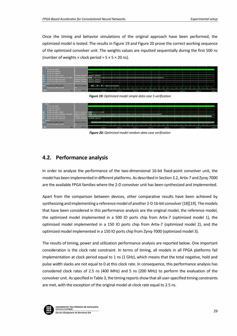
Once the timing and behavior simulations of the original approach have been performed, the
optimized model is tested. The results in Figure 19 and Figure 20 prove the correct working sequence
of the optimized convolver unit. The weights values are inputted sequentially during the first 500 ns
(number of weights × clock period = 5 × 5 × 20 ns).
Figure 19: Optimized model simple data case 5 verification
Figure 20: Optimized model random data case verification
4.2. Performance analysis
In order to analyze the performance of the two-dimensional 16-bit fixed-point convolver unit, the
model has been implemented in different platforms. As described in Section 3.2, Artix-7 and Zynq-7000
are the available FPGA families where the 2-D convolver unit has been synthesized and implemented.
Apart from the comparison between devices, other comparative results have been achieved by
synthesizing and implementing a reference model of another 2-D 16-bit convolver [18][19]. The models
that have been considered in this performance analysis are the original model, the reference model,
the optimized model implemented in a 500 IO ports chip from Artix-7 (optimized model 1), the
optimized model implemented in a 150 IO ports chip from Artix-7 (optimized model 2), and the
optimized model implemented in a 150 IO ports chip from Zynq-7000 (optimized model 3).
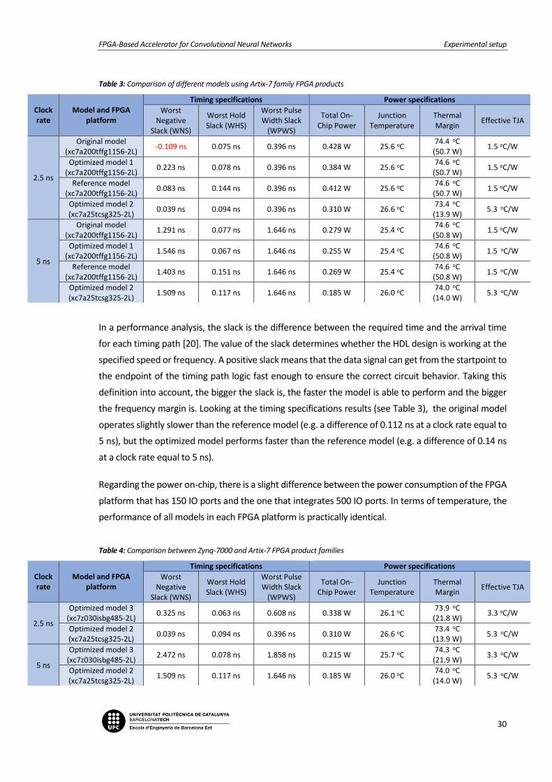
The results of timing, power and utilization performance analysis are reported below. One important
consideration is the clock rate constraint. In terms of timing, all models in all FPGA platforms fail
implementation at clock period equal to 1 ns (1 GHz), which means that the total negative, hold and
pulse width slacks are not equal to 0 at this clock rate. In consequence, this performance analysis has
considered clock rates of 2.5 ns (400 MHz) and 5 ns (200 MHz) to perform the evaluation of the
convolver unit. As specified in Table 3, the timing reports show that all user-specified timing constraints
are met, with the exception of the original model at clock rate equal to 2.5 ns.
FPGA-Based Accelerator for Convolutional Neural Networks Experimental setup
30
Table 3: Comparison of different models using Artix-7 family FPGA products
Clock rate
Model and FPGA platform
Timing specifications Power specifications
Worst Negative
Slack (WNS)
Worst Hold Slack (WHS)
Worst Pulse Width Slack
(WPWS)
Total On-Chip Power
Junction Temperature
Thermal Margin
Effective TJA
2.5 ns
Original model (xc7a200tffg1156-2L)
-0.109 ns 0.075 ns 0.396 ns 0.428 W 25.6 oC 74.4 oC
(50.7 W) 1.5 oC/W
Optimized model 1 (xc7a200tffg1156-2L)
0.223 ns 0.078 ns 0.396 ns 0.384 W 25.6 oC 74.6 oC
(50.7 W) 1.5 oC/W
Reference model (xc7a200tffg1156-2L)
0.083 ns 0.144 ns 0.396 ns 0.412 W 25.6 oC 74.6 oC
(50.7 W) 1.5 oC/W
Optimized model 2 (xc7a25tcsg325-2L)
0.039 ns 0.094 ns 0.396 ns 0.310 W 26.6 oC 73.4 oC
(13.9 W) 5.3 oC/W
5 ns
Original model (xc7a200tffg1156-2L)
1.291 ns 0.077 ns 1.646 ns 0.279 W 25.4 oC 74.6 oC
(50.8 W) 1.5 oC/W
Optimized model 1 (xc7a200tffg1156-2L)
1.546 ns 0.067 ns 1.646 ns 0.255 W 25.4 oC 74.6 oC
(50.8 W) 1.5 oC/W
Reference model (xc7a200tffg1156-2L)
1.403 ns 0.151 ns 1.646 ns 0.269 W 25.4 oC 74.6 oC
(50.8 W) 1.5 oC/W
Optimized model 2 (xc7a25tcsg325-2L)
1.509 ns 0.117 ns 1.646 ns 0.185 W 26.0 oC 74.0 oC
(14.0 W) 5.3 oC/W
In a performance analysis, the slack is the difference between the required time and the arrival time
for each timing path [20]. The value of the slack determines whether the HDL design is working at the
specified speed or frequency. A positive slack means that the data signal can get from the startpoint to
the endpoint of the timing path logic fast enough to ensure the correct circuit behavior. Taking this
definition into account, the bigger the slack is, the faster the model is able to perform and the bigger
the frequency margin is. Looking at the timing specifications results (see Table 3), the original model
operates slightly slower than the reference model (e.g. a difference of 0.112 ns at a clock rate equal to
5 ns), but the optimized model performs faster than the reference model (e.g. a difference of 0.14 ns
at a clock rate equal to 5 ns).
Regarding the power on-chip, there is a slight difference between the power consumption of the FPGA
platform that has 150 IO ports and the one that integrates 500 IO ports. In terms of temperature, the
performance of all models in each FPGA platform is practically identical.
Table 4: Comparison between Zynq-7000 and Artix-7 FPGA product families
Clock rate
Model and FPGA platform
Timing specifications Power specifications
Worst Negative
Slack (WNS)
Worst Hold Slack (WHS)
Worst Pulse Width Slack
(WPWS)
Total On-Chip Power
Junction Temperature
Thermal Margin
Effective TJA
2.5 ns
Optimized model 3 (xc7z030isbg485-2L)
0.325 ns 0.063 ns 0.608 ns 0.338 W 26.1 oC 73.9 oC
(21.8 W) 3.3 oC/W
Optimized model 2 (xc7a25tcsg325-2L)
0.039 ns 0.094 ns 0.396 ns 0.310 W 26.6 oC 73.4 oC
(13.9 W) 5.3 oC/W
5 ns
Optimized model 3 (xc7z030isbg485-2L)
2.472 ns 0.078 ns 1.858 ns 0.215 W 25.7 oC 74.3 oC
(21.9 W) 3.3 oC/W
Optimized model 2 (xc7a25tcsg325-2L)
1.509 ns 0.117 ns 1.646 ns 0.185 W 26.0 oC 74.0 oC
(14.0 W) 5.3 oC/W
FPGA-Based Accelerator for Convolutional Neural Networks Experimental setup
31
Due to Vivado license limitations with the Zynq-7000 family, only the optimized model has been
implemented with an FPGA platform of Zynq-7000 product family. The results of Table 4 show that the
optimized model operates faster in the Zynq-7000 platform, but it consumes a bigger amount of
power.
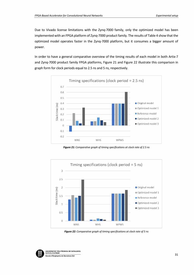
In order to have a general comparative overview of the timing results of each model in both Artix-7
and Zynq-7000 product family FPGA platforms, Figure 21 and Figure 22 illustrate this comparison in
graph form for clock periods equal to 2.5 ns and 5 ns, respectively.
Figure 21: Comparative graph of timing specifications at clock rate of 2.5 ns
Figure 22: Comparative graph of timing specifications at clock rate of 5 ns
FPGA-Based Accelerator for Convolutional Neural Networks Experimental setup
32
After implementation, the schematic is the easiest way to visualize the gates in a timing path [20]. In
order to have a general view of the implemented design, some schematics of the original model and
the optimized model are reported in Appendix B. The original model consists of 455 cells and 905 nets,
and the optimized model incorporates 71 cells and 137 nets. In comparison, the reference model
presents 480 cells and 938 nets.
As mentioned above, a positive slack indicates that the path meets its requirements, which depend on
the timing constraints. Each path of the design includes a source and a destination. The source defines
the path startpoint that launches the data, which is usually the clock pin of a sequential cell or an input
port. The destination corresponds to the path endpoint that captures the data, which is usually the
input data pin of the destination sequential cell or an output port [20]. Taking these definitions into
account, Table 5 presents the corresponding paths of each worst slack.
Table 5: Paths of the worst slack timing values
Clock rate
Model and FPGA platform
Timing specifications
Worst Negative
Slack (WNS) Corresponding path
2.5 ns
Original model (xc7a200tffg1156-2L)
-0.109 ns Source controlpath_unit/counter_reg[3]/C
Destination controlpath_unit/counter_reg[2]/D
Optimized model 1 (xc7a200tffg1156-2L)
0.223 ns Source controlpath_unit/counter_reg[3]/C
Destination controlpath_unit/counter_reg[2]/D
Optimized model 2 (xc7a25tcsg325-2L)
0.039 ns
Source datapath_unit/weight_register_0/count_reg[3]/C
Destination datapath_unit/weight_register_0/
weight_reg_reg[8][0]/CE
Optimized model 3 (xc7z030isbg485-2L)
0.325 ns Source datapath_unit/inter_register_0/data_reg_c_21/C
Destination datapath_unit/shift_register_4/data_reg[0][0]/D
5 ns
Original model (xc7a200tffg1156-2L)
1.291 ns Source controlpath_unit/counter_reg[3]/C
Destination controlpath_unit/counter_reg[6]/D
Optimized model 1 (xc7a200tffg1156-2L)
1.546 ns Source controlpath_unit/counter_reg[3]/C
Destination controlpath_unit/counter_reg[0]/D
Optimized model 2 (xc7a25tcsg325-2L)
1.509 ns Source controlpath_unit/counter_reg[3]/C
Destination controlpath_unit/counter_reg[0]/D
Optimized model 3 (xc7z030isbg485-2L)
2.472 ns
Source datapath_unit/weight_register_0/count_reg[4]/C
Destination datapath_unit/weight_register_0/
weight_reg_reg[11][12]/CE
Regarding utilization performance analysis, Table 6 corresponds to an overall description of the
number of hardware resources. The most significant highlights are that the designed convolver unit
uses less lookup tables (LUT) and more flip-flops (FF) than the reference model.
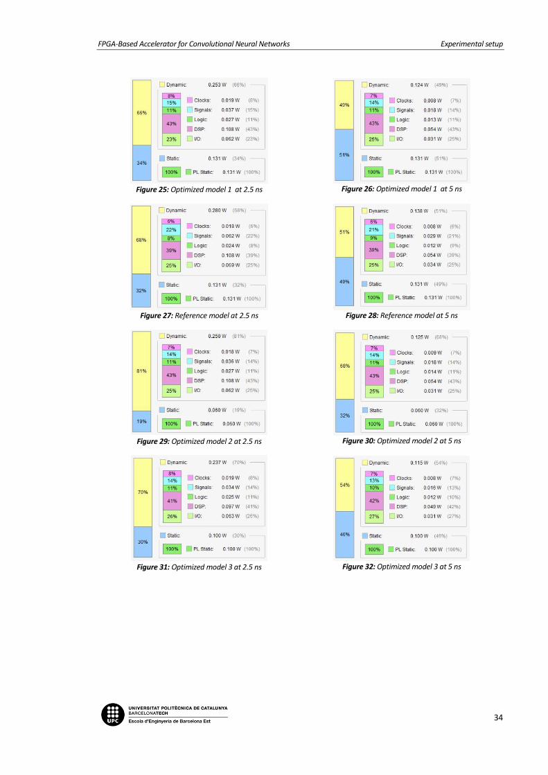
In order to conclude the performance analysis comparison, detailed pictures of the power
consumption of all the models in each FPGA platform with each clock rate are featured below. In
general terms, when operating at a clock period of 5 ns, the different models use practically half of the
power than the corresponding consumption at 2.5 ns clock rate. Another remarkable aspect is that the
FPGA-Based Accelerator for Convolutional Neural Networks Experimental setup
33
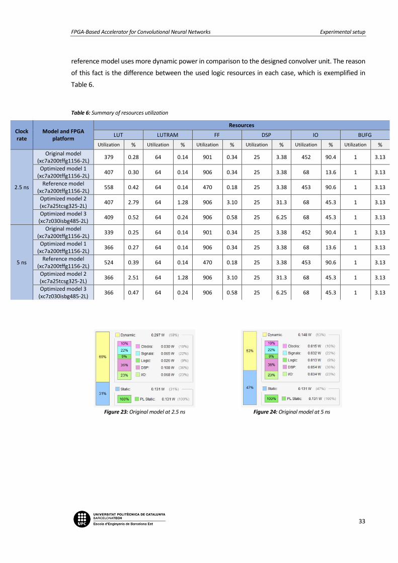
reference model uses more dynamic power in comparison to the designed convolver unit. The reason
of this fact is the difference between the used logic resources in each case, which is exemplified in
Table 6.
Table 6: Summary of resources utilization
Clock rate
Model and FPGA platform
Resources
LUT LUTRAM FF DSP IO BUFG
Utilization % Utilization % Utilization % Utilization % Utilization % Utilization %
2.5 ns
Original model (xc7a200tffg1156-2L)
379 0.28 64 0.14 901 0.34 25 3.38 452 90.4 1 3.13
Optimized model 1 (xc7a200tffg1156-2L)
407 0.30 64 0.14 906 0.34 25 3.38 68 13.6 1 3.13
Reference model (xc7a200tffg1156-2L)
558 0.42 64 0.14 470 0.18 25 3.38 453 90.6 1 3.13
Optimized model 2 (xc7a25tcsg325-2L)
407 2.79 64 1.28 906 3.10 25 31.3 68 45.3 1 3.13
Optimized model 3 (xc7z030isbg485-2L)
409 0.52 64 0.24 906 0.58 25 6.25 68 45.3 1 3.13
5 ns
Original model (xc7a200tffg1156-2L)
339 0.25 64 0.14 901 0.34 25 3.38 452 90.4 1 3.13
Optimized model 1 (xc7a200tffg1156-2L)
366 0.27 64 0.14 906 0.34 25 3.38 68 13.6 1 3.13
Reference model (xc7a200tffg1156-2L)
524 0.39 64 0.14 470 0.18 25 3.38 453 90.6 1 3.13
Optimized model 2 (xc7a25tcsg325-2L)
366 2.51 64 1.28 906 3.10 25 31.3 68 45.3 1 3.13
Optimized model 3 (xc7z030isbg485-2L)
366 0.47 64 0.24 906 0.58 25 6.25 68 45.3 1 3.13
Figure 23: Original model at 2.5 ns
Figure 24: Original model at 5 ns
FPGA-Based Accelerator for Convolutional Neural Networks Experimental setup
34
Figure 25: Optimized model 1 at 2.5 ns
Figure 26: Optimized model 1 at 5 ns
Figure 27: Reference model at 2.5 ns
Figure 28: Reference model at 5 ns
Figure 29: Optimized model 2 at 2.5 ns
Figure 30: Optimized model 2 at 5 ns
Figure 31: Optimized model 3 at 2.5 ns
Figure 32: Optimized model 3 at 5 ns
FPGA-Based Accelerator for Convolutional Neural Networks Conclusions and recommendations
35
Conclusions and recommendations
FPGAs are growing exponentially in terms of performance and size. Developing more efficient and
flexible hardware platforms to complement general-purpose processors offers a significant
improvement in the field of neural networks architectures regarding computational and energy
requirements.
In this report, we have focused on CNNs. More precisely, this thesis presents a two-dimensional 16-bit
fixed-point convolver unit. The implemented technique consists of a pipelined registers block that
allows obtaining one convolution operation result every clock cycle after an initialization stage. The
results of the timing, power and utilization reports show that the original and optimized models
achieve a level of performance capable of challenging the current state-of-the-art of 2-D convolvers.
Due to the required initialization stage to load the first image pixels, the main advantage of the
presented optimized model in comparison to the original and the reference models is the reduction of
the number of IO resources: the optimized approach uses around 85% less IO ports than the other
models.
Promising future work towards the improvement of the proposed 2-D convolver unit could be a deeper
analysis of the possibility of performing arbitrary data, kernel and image size convolutions, as well as
the possibility of adding extra pipeline stages in the multiplier module. Nevertheless, this second
possible improvement regarding pipelined multiplications should pay special attention to the
compromise between memory footprint and computational speed-up.
In the future, the main objective of this project is the implementation of the FPGA-based accelerator
for CNNs, which will incorporate this 2-D 16-bit fixed-point convolver approach.
FPGA-Based Accelerator for Convolutional Neural Networks References
36
References
[1] G. DInelli, G. Meoni, E. Rapuano, G. Benelli, and L. Fanucci, “An FPGA-Based Hardware Accelerator for CNNs Using On-Chip Memories Only: Design and Benchmarking with Intel Movidius Neural Compute Stick,” Int. J. Reconfigurable Comput., vol. 2019, 2019, doi: 10.1155/2019/7218758.
[2] S. Mittal, A survey of FPGA-based accelerators for convolutional neural networks, vol. 32, no. 4. Springer London, 2020.
[3] G. Feng, Z. Hu, S. Chen, and F. Wu, “Accelerator for Convolutional Neural Networks,” pp. 4–6, 2016.
[4] J. Qiu, J. Wang, S. Yao, K. Guo, and B. Li, “Going Deeper with Embedded FPGA Platform for Convolutional Neural Network • Deep Learning and Convolutional Neural Network – V2 : Brief introduction,” pp. 26–35, 2016, doi: 10.1145/2847263.2847265.
[5] C. Szegedy et al., “Going deeper with convolutions,” Proc. IEEE Comput. Soc. Conf. Comput. Vis. Pattern Recognit., vol. 07-12-June, pp. 1–9, 2015, doi: 10.1109/CVPR.2015.7298594.
[6] B. Bosi, G. Bois, and Y. Savaria, “Reconfigurable pipelined 2-D convolvers for fast digital signal processing,” IEEE Trans. Very Large Scale Integr. Syst., vol. 7, no. 3, pp. 299–308, 1999, doi: 10.1109/92.784091.
[7] A. Georgios, “Design and Implementation of an FPGA-Based Convolutional Neural Network Accelerator,” 2018.
[8] M. P. Hosseini, S. Lu, K. Kamaraj, A. Slowikowski, and H. C. Venkatesh, Deep Learning Architectures, vol. 866. 2020.
[9] “A Comprehensive Guide to Convolutional Neural Networks — the ELI5 way.” https://towardsdatascience.com/a-comprehensive-guide-to-convolutional-neural-networks-the-eli5-way-3bd2b1164a53 (accessed Jun. 15, 2020).
[10] Y. LeCun, L. Bottou, Y. Bengio, and P. Haffner, “Gradient-based learning applied to document recognition,” Proc. IEEE, vol. 86, no. 11, pp. 2278–2323, 1998, doi: 10.1109/5.726791.
[11] “LeNet-5 - A Classic CNN Architecture - engMRK.” https://engmrk.com/lenet-5-a-classic-cnn-architecture/ (accessed Jun. 18, 2020).
[12] “CS231n Convolutional Neural Networks for Visual Recognition.” https://cs231n.github.io/convolutional-networks/ (accessed Jun. 15, 2020).
[13] “An Intuitive Explanation of Convolutional Neural Networks – the data science blog.” https://ujjwalkarn.me/2016/08/11/intuitive-explanation-convnets/ (accessed Jun. 18, 2020).
[14] “Support Vector Machine — Introduction to Machine Learning Algorithms.” https://towardsdatascience.com/support-vector-machine-introduction-to-machine-learning-algorithms-934a444fca47 (accessed Jun. 18, 2020).
FPGA-Based Accelerator for Convolutional Neural Networks References
37
[15] “A Practical Guide to ReLU - Danqing Liu - Medium.” https://medium.com/@danqing/a-practical-guide-to-relu-b83ca804f1f7 (accessed Jun. 18, 2020).
[16] Xilinx, “7 Series FPGAs Data Sheet: Overview (DS180),” vol. 180, pp. 1–18, 2010, [Online]. Available: www.xilinx.com.
[17] Xilinx Inc., “Zynq-7000 SoC Data Sheet: Overview,” vol. 190, pp. 1–21, 2018, [Online]. Available: https://www.xilinx.com/support/documentation/data_sheets/ds190-Zynq-7000-Overview.pdf.
[18] L. T. Oliveira, M. S. Kim, A. A. Del Barrio, N. Bagherzadeh, and R. Menotti, “Design of power-efficient FPGA convolutional cores with approximate log multiplier,” ESANN 2019 - Proceedings, 27th Eur. Symp. Artif. Neural Networks, Comput. Intell. Mach. Learn., no. April, pp. 203–208, 2019.
[19] C. Farabet, C. Poulet, J. Y. Han, and Y. LeCun, “CNP: An FPGA-based processor for Convolutional Networks,” FPL 09 19th Int. Conf. F. Program. Log. Appl., vol. 1, no. 1, pp. 32–37, 2009, doi: 10.1109/FPL.2009.5272559.
[20] “Vivado Design Suite User Guide Design Analysis and Closure Techniques,” 2013. Accessed: Jun. 16, 2020. [Online]. Available: http://www.xilinx.com/warranty.htm#critapps.
FPGA-Based Accelerator for Convolutional Neural Networks Appendix A
38
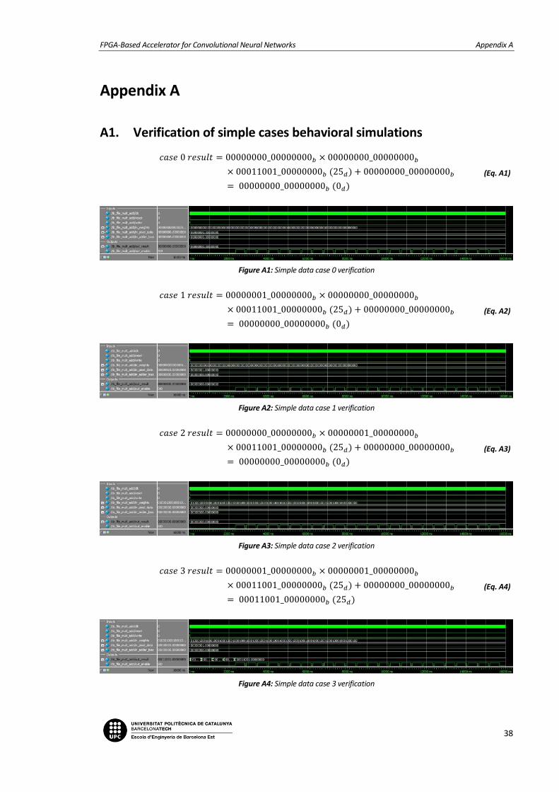
Appendix A
A1. Verification of simple cases behavioral simulations
𝑐𝑎𝑠𝑒 0 𝑟𝑒𝑠𝑢𝑙𝑡 = 00000000_00000000𝑏 × 00000000_00000000𝑏
× 00011001_00000000𝑏 (25𝑑) + 00000000_00000000𝑏
= 00000000_00000000𝑏 (0𝑑)
(Eq. A1)
Figure A1: Simple data case 0 verification
𝑐𝑎𝑠𝑒 1 𝑟𝑒𝑠𝑢𝑙𝑡 = 00000001_00000000𝑏 × 00000000_00000000𝑏
× 00011001_00000000𝑏 (25𝑑) + 00000000_00000000𝑏
= 00000000_00000000𝑏 (0𝑑)
(Eq. A2)
Figure A2: Simple data case 1 verification
𝑐𝑎𝑠𝑒 2 𝑟𝑒𝑠𝑢𝑙𝑡 = 00000000_00000000𝑏 × 00000001_00000000𝑏
× 00011001_00000000𝑏 (25𝑑) + 00000000_00000000𝑏
= 00000000_00000000𝑏 (0𝑑)
(Eq. A3)
Figure A3: Simple data case 2 verification
𝑐𝑎𝑠𝑒 3 𝑟𝑒𝑠𝑢𝑙𝑡 = 00000001_00000000𝑏 × 00000001_00000000𝑏
× 00011001_00000000𝑏 (25𝑑) + 00000000_00000000𝑏
= 00011001_00000000𝑏 (25𝑑)
(Eq. A4)
Figure A4: Simple data case 3 verification
FPGA-Based Accelerator for Convolutional Neural Networks Appendix A
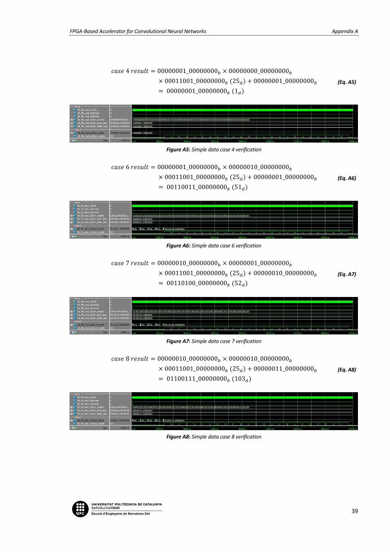
39
𝑐𝑎𝑠𝑒 4 𝑟𝑒𝑠𝑢𝑙𝑡 = 00000001_00000000𝑏 × 00000000_00000000𝑏
× 00011001_00000000𝑏 (25𝑑) + 00000001_00000000𝑏
= 00000001_00000000𝑏 (1𝑑)
(Eq. A5)
Figure A5: Simple data case 4 verification
𝑐𝑎𝑠𝑒 6 𝑟𝑒𝑠𝑢𝑙𝑡 = 00000001_00000000𝑏 × 00000010_00000000𝑏
× 00011001_00000000𝑏 (25𝑑) + 00000001_00000000𝑏
= 00110011_00000000𝑏 (51𝑑)
(Eq. A6)
Figure A6: Simple data case 6 verification
𝑐𝑎𝑠𝑒 7 𝑟𝑒𝑠𝑢𝑙𝑡 = 00000010_00000000𝑏 × 00000001_00000000𝑏
× 00011001_00000000𝑏 (25𝑑) + 00000010_00000000𝑏
= 00110100_00000000𝑏 (52𝑑)
(Eq. A7)
Figure A7: Simple data case 7 verification
𝑐𝑎𝑠𝑒 8 𝑟𝑒𝑠𝑢𝑙𝑡 = 00000010_00000000𝑏 × 00000010_00000000𝑏
× 00011001_00000000𝑏 (25𝑑) + 00000011_00000000𝑏
= 01100111_00000000𝑏 (103𝑑)
(Eq. A8)
Figure A8: Simple data case 8 verification
FPGA-Based Accelerator for Convolutional Neural Networks Appendix A
40
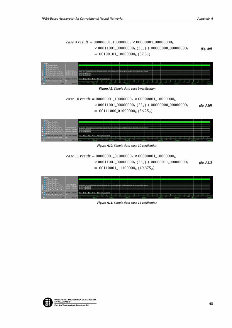
𝑐𝑎𝑠𝑒 9 𝑟𝑒𝑠𝑢𝑙𝑡 = 00000001_10000000𝑏 × 00000001_00000000𝑏
× 00011001_00000000𝑏 (25𝑑) + 00000000_00000000𝑏
= 00100101_10000000𝑏 (37.5𝑑)
(Eq. A9)
Figure A9: Simple data case 9 verification
𝑐𝑎𝑠𝑒 10 𝑟𝑒𝑠𝑢𝑙𝑡 = 00000001_10000000𝑏 × 00000001_10000000𝑏
× 00011001_00000000𝑏 (25𝑑) + 00000000_00000000𝑏
= 00111000_01000000𝑏 (56.25𝑑)
(Eq. A10)
Figure A10: Simple data case 10 verification
𝑐𝑎𝑠𝑒 11 𝑟𝑒𝑠𝑢𝑙𝑡 = 00000001_01000000𝑏 × 00000001_10000000𝑏
× 00011001_00000000𝑏 (25𝑑) + 00000011_00000000𝑏
= 00110001_11100000𝑏 (49.875𝑑)
(Eq. A11)
Figure A11: Simple data case 11 verification
FPGA-Based Accelerator for Convolutional Neural Networks Appendix B
41
Appendix B
B1. Schematic of the original model
Figure B1: Original model implemented design device
Figure B2: Part of the original model schematic
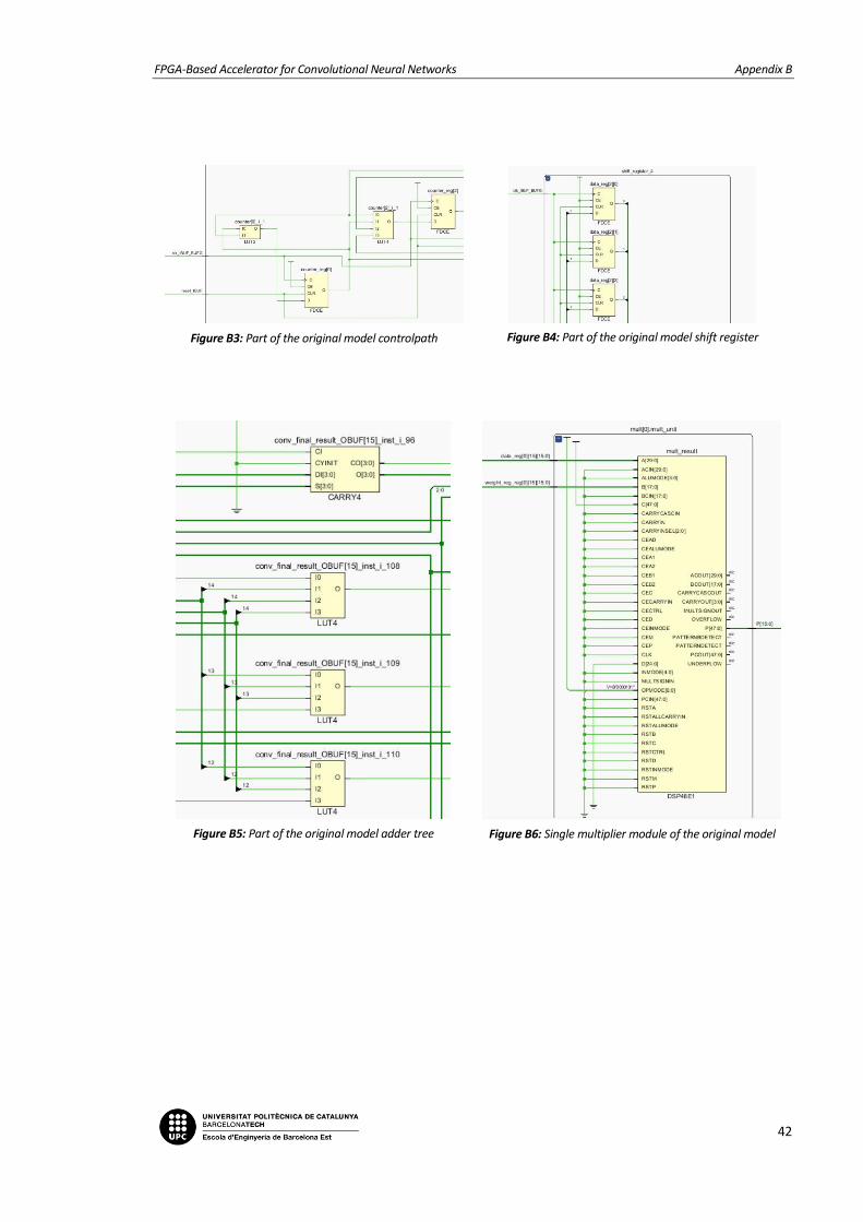
FPGA-Based Accelerator for Convolutional Neural Networks Appendix B
42
Figure B3: Part of the original model controlpath
Figure B4: Part of the original model shift register
Figure B5: Part of the original model adder tree
Figure B6: Single multiplier module of the original model
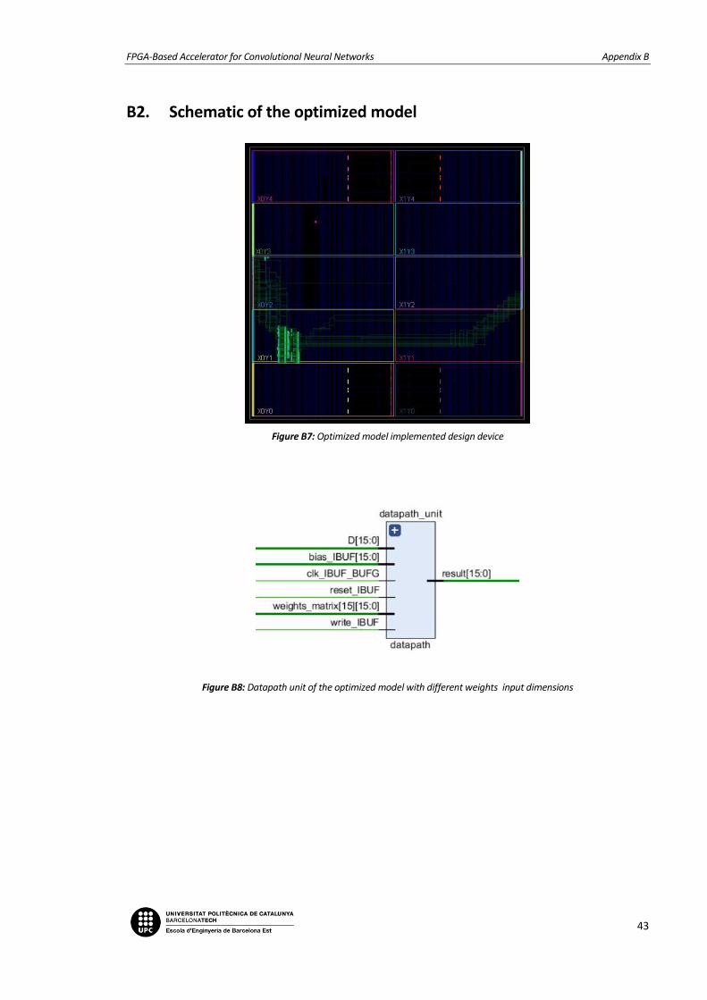
FPGA-Based Accelerator for Convolutional Neural Networks Appendix B
43
B2. Schematic of the optimized model
Figure B7: Optimized model implemented design device
Figure B8: Datapath unit of the optimized model with different weights input dimensions