Embed Size (px)
Citation preview

High-efficiency Microwave Power Amplifiers Through
Passive and Active Harmonic Control
by
Sushians Rahimizadeh
M.S., University of Colorado at Boulder, 2016
B.S., University of Colorado at Boulder, 2013
A thesis submitted to the
Faculty of the Graduate School of the
University of Colorado in partial fulfillment
of the requirements for the degree of
Doctor of Philosophy
Department of Electrical, Computer, and Energy Engineering
May 2019

ProQuest Number:
All rights reserved
INFORMATION TO ALL USERSThe quality of this reproduction is dependent upon the quality of the copy submitted.
In the unlikely event that the author did not send a complete manuscriptand there are missing pages, these will be noted. Also, if material had to be removed,
a note will indicate the deletion.
ProQuest
Published by ProQuest LLC ( ). Copyright of the Dissertation is held by the Author.
All rights reserved.This work is protected against unauthorized copying under Title 17, United States Code
Microform Edition © ProQuest LLC.
ProQuest LLC.789 East Eisenhower Parkway
P.O. Box 1346Ann Arbor, MI 48106 - 1346
22615304
22615304
2019

This thesis entitled:
High-efficiency Microwave Power Amplifiers Through Passive and Active Harmonic Control
written by Sushians Rahimizadeh
has been approved for the Department of Electrical, Computer, and Energy Engineering
Zoya Popovic
Taylor Barton
Date
The final copy of this thesis has been examined by the signatories, and we
find that both the content and the form meet acceptable presentation standards
of scholarly work in the above mentioned discipline.

Rahimizadeh, Sushians (Ph.D., Electrical Engineering)
High-efficiency Microwave Power Amplifiers Through Passive and Active Harmonic Control
Thesis directed by Professor Zoya Popovic
The design of the next generation of microwave transmitters must advance in stride with
state-of-the-art radar, communication, and remote-sensing systems. As the performance of high-
frequency transmitters improves, so too do the systems and the science which rely on them. Among
the forefront of challenges facing the design of active microwave components is that of enabling
highly-efficient operation. Doing so demands the application of a breadth of circuit and elec-
tromagnetic theory to overcome pragmatic limitations imposed by factors such as lossy circuit
elements, non-linear reactances, and parasitic impedances. The praxis of active and passive mi-
crowave design to high-frequency power amplifiers (PAs) serves to further the state-of-the-art and
empower the industry to which it is applied. Gainful applications of highly-efficient PAs lie in
both communication and sensing. In satellite transmitters, e.g., power and volume is significantly
limited, and the communication of data to terrestrial networks is directly affected by the efficiency
of the transmitter PA.
Non-linear microwave power transistors inherently generate power at harmonic frequencies.
In this work, harmonic power is controlled with both passive and active impedances in order
to precisely engineer current and voltage waveforms at the current generator plane. Transistor
packages present highly-reactive impedances that significantly limit harmonic control, but can also
be used as a part of the matching network. In the L- and S-band PAs demonstrated in this thesis,
bond-wires and package parasitics are analyzed with full-wave EM simulations and used to control
amplitude and phase of up to 3 harmonics. This results in compact, highly-efficient in-package PAs
with efficiencies ranging from 65% to 80% at around 10-W output power. Methodology is developled
which can be applied to any package and transistor with known geometry and non-linear model.
In addition to passively terminating harmonic frequencies, active terminations are investigated as
a means to obtain efficiency and linearity, and a comparison between the two performed.
iii

Contents
Table of Contents iv
List of Tables vii
List of Figures viii
1 Introduction 1
1.1 Motivation . . . . . . . . . . . . . . . . . . . . . . . . . . . . . . . . . . . . . . . . 4
1.2 Design methods for High-efficiency amplifiers . . . . . . . . . . . . . . . . . 6
1.3 Thesis Organization . . . . . . . . . . . . . . . . . . . . . . . . . . . . . . . . . . 7
2 Non-linear Packaged Device Characterization 10
2.1 Load-pull Simulation and Measurement . . . . . . . . . . . . . . . . . . . . . 11
2.2 Harmonic Waveform Shaping . . . . . . . . . . . . . . . . . . . . . . . . . . . . . 16
2.3 Other modeling and characterization approaches . . . . . . . . . . . . . . 20
3 Package Modeling 22
3.1 Package Modeling . . . . . . . . . . . . . . . . . . . . . . . . . . . . . . . . . . . 23
3.2 Tab Capacitance . . . . . . . . . . . . . . . . . . . . . . . . . . . . . . . . . . . . . 24
3.2.1 Lumped Capacitors . . . . . . . . . . . . . . . . . . . . . . . . . . . . . . . 25
3.2.2 Bond-wires . . . . . . . . . . . . . . . . . . . . . . . . . . . . . . . . . . . . 26
3.3 Limitations of Commercial Packages . . . . . . . . . . . . . . . . . . . . . . . 29
4 Package Design and Validation 33
iv

4.1 In-package Matching Topologies . . . . . . . . . . . . . . . . . . . . . . . . . . 35
4.2 In-package Harmonic Termination Fidelity . . . . . . . . . . . . . . . . . . . 37
4.3 Harmonically Pre-matched Package . . . . . . . . . . . . . . . . . . . . . . . . 40
4.4 Harmonically-terminated Package Design . . . . . . . . . . . . . . . . . . . . 41
4.5 Passive Package Validation . . . . . . . . . . . . . . . . . . . . . . . . . . . . . 44
4.5.1 Full-Wave Simulations . . . . . . . . . . . . . . . . . . . . . . . . . . . . 45
4.5.2 Experimental Validation . . . . . . . . . . . . . . . . . . . . . . . . . . . 47
4.6 Active Package Measurements . . . . . . . . . . . . . . . . . . . . . . . . . . . 50
5 Power Amplifier In a Package 54
5.1 Class-F LDMOS Package . . . . . . . . . . . . . . . . . . . . . . . . . . . . . . . 55
5.2 Class-F−1 GaN Package . . . . . . . . . . . . . . . . . . . . . . . . . . . . . . . . 58
5.2.1 Design Methodology for GaN class-F−1 in a package . . . . . . . . 59
5.2.2 Class-F−1 GaN PA Design . . . . . . . . . . . . . . . . . . . . . . . . . . 61
5.2.3 In-package Stability . . . . . . . . . . . . . . . . . . . . . . . . . . . . . . 66
5.3 Conclusion . . . . . . . . . . . . . . . . . . . . . . . . . . . . . . . . . . . . . . . . 72
6 Harmonic Injection 74
6.1 HI-PA Design . . . . . . . . . . . . . . . . . . . . . . . . . . . . . . . . . . . . . . . 75
6.1.1 Bias-tee Design . . . . . . . . . . . . . . . . . . . . . . . . . . . . . . . . . 76
6.1.2 Output Network Design . . . . . . . . . . . . . . . . . . . . . . . . . . . 77
6.2 HI-PA Measurements . . . . . . . . . . . . . . . . . . . . . . . . . . . . . . . . . . 80
6.3 Linearity Measurements . . . . . . . . . . . . . . . . . . . . . . . . . . . . . . . 86
6.4 Conclusion . . . . . . . . . . . . . . . . . . . . . . . . . . . . . . . . . . . . . . . . 86
7 Conclusions and Future Work 88
7.1 Thesis Summary and Contributions . . . . . . . . . . . . . . . . . . . . . . . . . 88
7.2 Future Work . . . . . . . . . . . . . . . . . . . . . . . . . . . . . . . . . . . . . . . 91
v

Bibliography 96
A Compact High-Gain CubeSat Antenna 107
A.1 Feed Miniaturization . . . . . . . . . . . . . . . . . . . . . . . . . . . . . . . . . . 109
vi

List of Tables
1.1 Comparison of LDMOS Performance between 1-4 GHz . . . . . . . . . . . . . . . . . 7
4.1 Circuit element values for the three circuits in Fig. 4.3. . . . . . . . . . . . . . . . . . 35
4.2 Three cases for harmonic resonator values . . . . . . . . . . . . . . . . . . . . . . . . 41
4.3 Circuit model element values for designs A-E . . . . . . . . . . . . . . . . . . . . . . 44
4.4 Circuit model element values . . . . . . . . . . . . . . . . . . . . . . . . . . . . . . . 48
5.1 Circuit model element values for Class-F Package . . . . . . . . . . . . . . . . . . . . 58
5.2 Circuit model element values for the class-F−1 package output network, as deter-
mined from Sec. 5.2.2 (synthesized) and as adjusted for practical implementation
(adjusted). . . . . . . . . . . . . . . . . . . . . . . . . . . . . . . . . . . . . . . . . . 64
vii

List of Figures
1.1 Power Amplifier architectures for enabling high-efficiency communication transmit-
ters: (a) Single-ended harmonically-termianted PA, (b) Supply-modulated PA ,(c)
Outphasing PA, (d) Doherty PA 1.1d, and (e) the Harmonic Injection PA. . . . . . . 2
1.2 (a) Photo of a typical high-power packaged transistor for operation around 2 GHz.
(b) Block diagram of the output side of a PA using a packaged transistor, with
relevant reference planes labeled. The current and voltage waveforms are calculated
from the package in Fig.1, starting from class-F waveforms approximated with a 2nd
and 3rd at the virtual drain plane. . . . . . . . . . . . . . . . . . . . . . . . . . . . . 5
1.3 The transformed constellation presented at the Die Plane at 2f0 (blue) and 3f0
(green) and at the Virtual Drain plane for commercial package at 2.6 GHz. This
illustrates the limited range of passive impedances that can be reached by matching
outside of the package. . . . . . . . . . . . . . . . . . . . . . . . . . . . . . . . . . . . 6
2.1 Fundamental LP simulation setup and non-linear model of packaged device PTFC260202FC
at 2.6 GHz (a), constellation of impedance points presented during LP (b), Funda-
mental SP (c) and LP (d) PAE contours at a fixed input power (20 dBm). . . . . . 12
2.2 Simulated PAE contours for 2nd harmonic SP (a) and LP (b), and 3rd harmonic LP
(c) on 50-Ω Smith charts. Impedance for max PAE is indicated by the marker. . . . 13
viii

2.3 LP and SP measurement setup using fundamental-only passive single-slug Focus
tuners, with capabilities for power, bias, and frequency sweeps. LP fixtures include
a bias tee and transform 50-Ω line to a trace of width of package lead, and include a
bias tee and a 2nd harmonic termination open-circuit stub on the load. Power meters
measure fundamental power. The grey dashed line encapsulates the portion of the
setup that is de-embedded, allowing measurement at the DUT reference plane. . . . 14
2.4 Picture of the LP setup described in Fig. 2.3 (a). The LP constellation (55 points)
is shown in (b). . . . . . . . . . . . . . . . . . . . . . . . . . . . . . . . . . . . . . . . 14
2.5 Fixures used in load-pull to mount the device under test. The gap in the middle
defines the reference plane of the package terminals. In the photo, the left side of
this break-apart fixture includes the gate bias line. A similar circuit is made for the
drain. The tapers without the bias lines serve as calibration standards to de-embed
measurements to the package plane. . . . . . . . . . . . . . . . . . . . . . . . . . . . 15
2.6 Measured LP contours for Pout, Gain, and PAE on 50-Ω Smith charts. . . . . . . . . 16
2.7 Measured drive-up curve with load impedance set to corresponding to the maximum
PAE found from LP (Fig. 2.6). . . . . . . . . . . . . . . . . . . . . . . . . . . . . . . 16
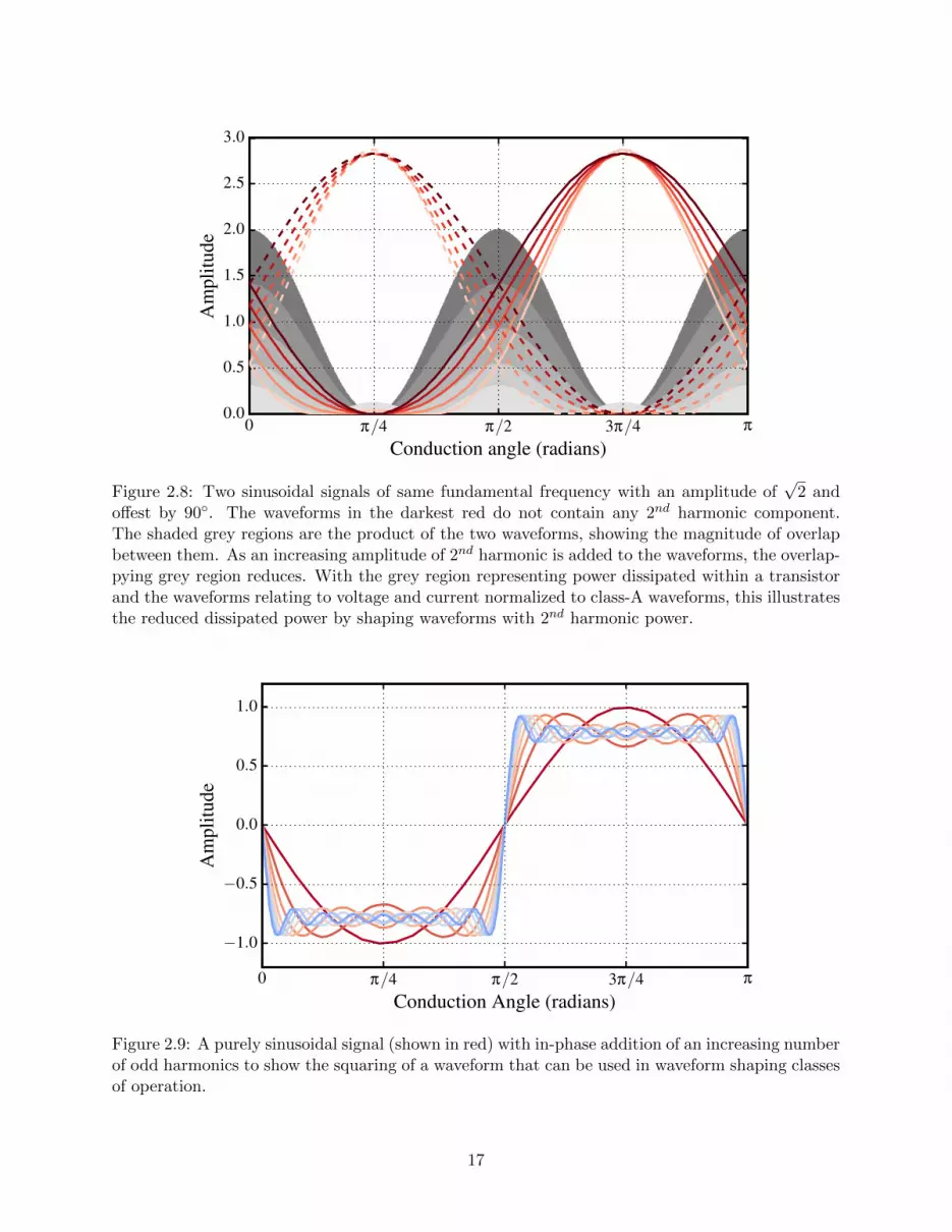
2.8 Two sinusoidal signals of same fundamental frequency with an amplitude of√
2 and
offest by 90. The waveforms in the darkest red do not contain any 2nd harmonic
component. The shaded grey regions are the product of the two waveforms, showing
the magnitude of overlap between them. As an increasing amplitude of 2nd harmonic
is added to the waveforms, the overlappying grey region reduces. With the grey
region representing power dissipated within a transistor and the waveforms relating
to voltage and current normalized to class-A waveforms, this illustrates the reduced
dissipated power by shaping waveforms with 2nd harmonic power. . . . . . . . . . . . 17
2.9 A purely sinusoidal signal (shown in red) with in-phase addition of an increasing
number of odd harmonics to show the squaring of a waveform that can be used in
waveform shaping classes of operation. . . . . . . . . . . . . . . . . . . . . . . . . . 17
ix

2.10 The effect of the shaped voltage (green) and current (blue) waveforms when the
2nd and 3rd harmonic are reflected out of phase with respect to the fundamental
component. The optimum amplitude and phase of the harmonics which lead to the
smallest degree of dissipated power [9] lead to the waveforms shown in the darkest
green and blue, with the corresponding mininum dissipated power outlined in grey.
The increasing overlap of voltage and current as the termination phase approaches
90 is shown in red, illustrating the need for precise harmonic phase reflections. . . . 18
2.11 As a method for performing 2f0 loadpull, 4 discrete 2f0 impedances are presented to
the package by varying the length of an open-circuit microstrip stub that is responible
for the phase of the 2f0 termination. At each 2f0 impedance (marked by an ’x’
of color corresponding to the stub length labeled in the inset), an f0 loadpull is
performed, and the maximum measured PAE is labeled by the corresponding cross. 20
3.1 Commercially available packaged 10-W LDMOS power transistor showing the bond-
wires that connect the gate and drain manifolds to the package lead via a shunt
MOS capacitor that, together with bond-wire inductance, provides pre-matching at
2.6 GHz. The significant parasitic reactances, present in any metal-ceramic package,
are labeled in various intensities of red corresponding to relative values of the parasitics. 23
3.2 HFSS setup (b) of segment of package of H-37248-4 package where frame, lead,
metallization, and flange overlap (a) shown by red dashed line. . . . . . . . . . . . . 24
3.3 HFSS simulation of a straight PEC 100-mil bond-wire (a) and an array of bond-wires
(b). . . . . . . . . . . . . . . . . . . . . . . . . . . . . . . . . . . . . . . . . . . . . . . 27
3.4 The equivalent series inductance of multiple bond-wires is examined in simulation
by sweeping the (a) seperation and (b) angle between wires. . . . . . . . . . . . . . . 28
3.5 A variety of bond-wire profiles and configurations were simulated and fabricated to
test available practical geometries. . . . . . . . . . . . . . . . . . . . . . . . . . . . . 30
x

3.6 Simulation of the gate network of the commercial package from package lead to die
plane, showing package pre-match (ΓHFSS). This is compared to the impedance
determined from the non-linear model (0.8 + j2.85,Ω) of die that corresponds to
max Pout (ΓAWR). . . . . . . . . . . . . . . . . . . . . . . . . . . . . . . . . . . . . . 31
3.7 The HFSS simulated S11 of the load-side network package plotted in grey. Red,
blue, and green crosses indicate the impedance at corresponding to f0, 2f0, and 3f0
respectively. . . . . . . . . . . . . . . . . . . . . . . . . . . . . . . . . . . . . . . . . . 31
3.8 The HFSS simmulated S-parameters of the load-side network (dashed line) of the
commercial package are fit to a circuit model, with determined element values shown. 32
4.1 The in-package network topology for gate and/or drain, with the lowest complexity
shown in black. The network can be extended to a 2nd-order low-pass filter with the
possibility of higher orders for larger packages. A series shunt tank circuit (shown in
grey) can be placed at each node if higher complexity is needed. The tab capacitance
Ctab is fixed for a given package geometry. . . . . . . . . . . . . . . . . . . . . . . . . 34
4.2 Transistor package 240 (a), package 280 (b), and package 110 (c), named for the
length in mils between gate and drain tabs. . . . . . . . . . . . . . . . . . . . . . . . 35
4.3 Impedances presented at the package output reference plane at the fundamental
(red), 2nd (blue), and 3rd (green) harmonics when a single element of the network
is varied according to Table 4.1. (a) Single series bond-wire, (b) T -network with
a shunt capacitor, and (c) T -network with additional shunt resonator. The tuner
reflection coefficient is limited to 0.4 in this example. . . . . . . . . . . . . . . . . . . 36
4.4 Lumped-element circuit model of an in-package open-circuit termination. At reso-
nance, the shunt LC network presents a short-circuit to be transformed to an open-
circuit by the impedance inverter formed by Lx and Cx. The resonator bond-wire
loss is modeled by RLa . . . . . . . . . . . . . . . . . . . . . . . . . . . . . . . . . . . 38
xi

4.5 The reflection coefficient magnitude of the harmonic termination in Fig. 4.4 is plotted
for a range of values for Lx and 3 different cases of resonator bond-wire loss. The
|Γ| ≥ 0.8 condition to maintain reasonably high efficiency is plotted in dashed gray as
a guideline for the trade-off between series bond-wire current handling and achieving
sufficiently high termination fidelity. . . . . . . . . . . . . . . . . . . . . . . . . . . . 38
4.6 (a) An ideal lumped-element Class-F−1 in-package matching network, with shunt the
L0C0 and L1C1 resonators serving as the 3f0 and 2f0 termination, respectivly. The
values for the resonators are listed in Table 4.2 for 3 different cases. The impedance
presented to the die, using the compromise case values, is plotted with resistance
increasing from 0 to 0.5 Ω in 0.1 Ω steps for bond-wire Ls0 (b) and L0 (c) . . . . . . 39
4.7 Harmonic pre-match package layout as simulated in HFSS (a) and the equivalent
circuit at both the gate and drain (b). . . . . . . . . . . . . . . . . . . . . . . . . . . 41
4.8 Simulated f0 and 2f0 tuning range at die reference plane, considering both the LP
fixture (simulated in Axium) and the package including in-package network (simu-
lated in HFSS). The black ’x’ on the f0 Smith chart indicate the max PAE impedance
as determined in simulated LP for this die. . . . . . . . . . . . . . . . . . . . . . . . 42
4.9 Measured (left) and simulated (right) loadpull contours at 2f0 on 17 Ω Smith charts,
referenced at the package reference plane. Measured load tuner impedances are
shown in grey. . . . . . . . . . . . . . . . . . . . . . . . . . . . . . . . . . . . . . . . 42
4.10 Simulated PAE load-pull contours at 2f0 for the 10-W LDMOS device at the die
reference plane at 2.6 GHz. The 2f0 terminations for each of the 5 package designs
are indicated by the grey dots (A-E). . . . . . . . . . . . . . . . . . . . . . . . . . . . 43
xii

4.11 (a) Transistor package for an Infineon 10-W LDMOS device with a fundamental of
2.6 GHz. The package is custom designed for a fundamental pre-match and a 2nd
harmonic termination both internal to the package. (b) Passive validation package,
where the active device is replaced by a capacitor of similar size and known value.
Circuit diagrams are also shown, where the inductors represent bond-wires and the
drain and gate tabs are represented by capacitors. . . . . . . . . . . . . . . . . . . . 46
4.12 HFSS model of the passive-only in-packaged matching circuit showing a plot of 2f0
of surface current magnitude along the bond wires and on the capacitor plates. The
current along L0 is pronounced (600 A/m), since it is responsible for the 2f0 drain
termination. Notice that there is more current on the bond-wire closest to L0 than
the other bond-wire at that point in the network. This is due to mutual inductance. 47
4.13 Microstrip fixture used for TRL calibration and measurement of the validation pack-
age. The package is mounted on a 280-mil wide microstrip line and tapered to a 50 Ω
environment. Bias-tees are integrated into the fixture anticipating large-signal mea-
surements with the active package but are not necessary for the validation process. . 48
4.14 Equivalent circuit model of passive package shown in Fig. 4.11b. The active device in
Fig. 4.11a is replaced by a capacitor CD of similar size and known value, represented
by capacitor CD in grey. . . . . . . . . . . . . . . . . . . . . . . . . . . . . . . . . . . 48
4.15 Measured (solid line) vs. simulated (dashed line) S21 of the equivalent package circuit
model from Fig.4. The elements Cmut and Lmut are omitted from this circuit model
and also plotted (dotted line) to illustrate the distinct impact of these values on the
impedance presented to the packaged device. . . . . . . . . . . . . . . . . . . . . . . 49
4.16 Measured (solid line) vs. simulated (dashed line) |S11| of the equivalent package
circuit model from Fig.4. The elements Cmut and Lmut are omitted from this circuit
model and also plotted (dotted line) to illustrate the distinct impact of these values
on the impedance presented to the packaged device. . . . . . . . . . . . . . . . . . . 50
xiii

4.17 Matching networks from Table 1 realized within a package. Three distinct packages
networks are shown, with varying element values: (a) designs A and C, (c) design
B, and (b) designs D and E. . . . . . . . . . . . . . . . . . . . . . . . . . . . . . . . . 52
4.18 Load-pull contours for constant PAE for varied fundamental (red scale) and 2nd
harmonic (blue scale) load impedance. The impedance presented to the device drain
terminal by the in-package passive circuit from Fig. 4.11b over the 1 to 8 GHz fre-
quency range is shown by the dashed gray trace, with the f0 and 2f0 impedances
indicated by the red and blue crosses, respectively. . . . . . . . . . . . . . . . . . . . 53
4.19 Fundamental frequency constant PAE contours (referenced at the die plane) for each
package shown in colors corresponding to each package design. The maximum PAE
measured during f0 loadpull of each package is shown beside its corresponding 2f0
termination (colored circle). The f0 impedance presented to the drain of the die for
each package design is shown by colored squares. . . . . . . . . . . . . . . . . . . . . 53
5.1 Simulated 3f0 load-pull contours for PAE at the die plane of the LDMOS device
used in the Class-F package with a fundamental of (a) 1.5 GHz and (b) 1.0 GHz,
where it can be seen that even at 1.5 GHz, there is insufficient harmonic content for
waveform shaping. A design frequency of 1.0 GHz is chosen since a variation of 5
points of PAE is seen in (b). . . . . . . . . . . . . . . . . . . . . . . . . . . . . . . . 56
5.2 (a) Photo of the fabricated Class-F package design (which uses the standard package
in Fig. 4.2b which has a 280-mil wide tab), and (b) the equivalent circuit model (b),
with element values shown in Table 5.1. The 2f0 and 3f0 resonators are shown in
the red and green boxes, respectively. Ls0 and Cp1 are designed to provide the phase
transformation of the 3f0 short to an open at the virtual drain considering the device
output capacitance (shown in grey). (c) The simulated return loss of each in-package
resonator. . . . . . . . . . . . . . . . . . . . . . . . . . . . . . . . . . . . . . . . . . . 57
xiv

5.3 Class-F package load-pull contours of constant PAE and Pout measured and de-
embedded to the package plane. Input power is constant at 22 dBm. . . . . . . . . . 59
5.4 Equivalent circuit for a class-F−1 in a package. . . . . . . . . . . . . . . . . . . . . . 61
5.5 Layout of the 25-W Qorvo GaN die with gate and drain pads labeled. The die
includes 2 cells of 4 375-µm gate fingers, with gate bondpads to each cell. The
gates of the cells also lead to additional, parallel bondpands connected by a 5 Ω TaN
resistor. Courtesy of Qorvo. . . . . . . . . . . . . . . . . . . . . . . . . . . . . . . . . 61
5.6 The extracted output capacitance Cout with swept gate voltage. At the chosen bias
point, Cout is approximated to be 0.41 pF. This is were the slope of Cout is the
greatest, indicating a large degree of non-linearty and therefore harmonic content. . 62
5.7 The simulated PAE contours at the die reference plane for LP at (a) f0, (b) 2f0,
and (c) 3f0. . . . . . . . . . . . . . . . . . . . . . . . . . . . . . . . . . . . . . . . . . 63
5.8 The 2f0 LP contours of constant PAE of Fig. 5.7b deembeded to the virtual drain,
indicating that the device prefers a 2f0 open, with the cross symbol indicating the
peak efficiency impedance. . . . . . . . . . . . . . . . . . . . . . . . . . . . . . . . . . 64
5.9 The physical realization of the drain network using package parasitics, device intrinsic
capacitance, bond-wires, and capacitors to present Class-F−1 impedances to the
virtual drain. . . . . . . . . . . . . . . . . . . . . . . . . . . . . . . . . . . . . . . . . 65
5.10 (a) The input impedance of the drain network using the ideal, lossless circuit model.
(b) The impedance presented by the device using the same circuit model but with
an additional 0.2 Ω reflecting the HFSS simulated drain network of Fig. 5.9. The
markers m1, m7, and m5 indicate f0, 2f0, and 3f0 impedance, respectively. . . . . . 66
5.11 The physical realization of the gate network in HFSS (before the addition of the
stability network) which matches to the complex input impedance of the device
without the use of an package-external matching network. . . . . . . . . . . . . . . . 67
xv

5.12 The simulated k-factor (orange) and Gmax (blue) of the chosen GaN device over a
wide range of frequencies for the scenario with (a) no stability network, (b) external
stability network consisting of a parallel RC network (R = 20 Ω, C = 0.1 pF ), and
(c) an internal stability network by a shunt RLC. In each case, the transistor is
presented with the designed gate and drain matching networks . . . . . . . . . . . . 68
5.13 The physical realization of the source network including internal stability network of
Fig. 5.12c for 2 different manifistations of the drain network 3f0 resonator: (a) with-
out adjusting the drain network of Fig. 5.9 but with undesireable coupling between
the gate and drain network, and (b) redesign of the 3f0 resonator with undesireable
coupling of the resonator to the drain fundamental match. . . . . . . . . . . . . . . 69
5.14 The final circuit model of the gate network including in-package stability elements
(a) with the corresponding k-factor (orange) and Gmax (blue) is plotted over a wide
range of frequencies (b). . . . . . . . . . . . . . . . . . . . . . . . . . . . . . . . . . 70
5.15 The entire Class-F−1 package design shown in HFSS (a) with equivalent circuit
model shown in (b). . . . . . . . . . . . . . . . . . . . . . . . . . . . . . . . . . . . . 71
5.16 Harmonic balance simulation using the HFSS-simulated S-parameters of the package
network shown in Fig 5.15a and the non-linear model device. The input power is
swept and the PAE (red), input power (pink) and transducer gain (blue) is plotted. 72
6.1 Block diagram of the HI-PA. When driven into compression with a two-tone signal,
the PA operates efficiently but not linearly. By injecting into the output a two-tone
signal with a doubled carrier frequency (2f0) and tone spacing (2∆f), IMD3 can be
reduced while maintaining efficiency through waveform shaping. . . . . . . . . . . . . 75
6.2 Photograph of the fabricated 2.3-GHz HI-PA on Rogers 4350B substrate and copper
baseplate. The board size is 106 mm × 76 mm. . . . . . . . . . . . . . . . . . . . . . 76
6.3 Isolation between the DC and the RF path from 0.5 to 10 GHz, showing a high
bias-line impedance across a bandwidth of greater than 10 GHz (including up to 3f0). 77
xvi

6.4 The impedance presented by the bias line to the RF path, plotted from 2 to 10 GHz.
The bias line is high-impedance over a large range of frequencies, with 2f0 near an
open circuit. . . . . . . . . . . . . . . . . . . . . . . . . . . . . . . . . . . . . . . . . . 78
6.5 The baseband resistance of the bias-line for the case where Lb is parallel resonant
at f0 (red) and 2f0 (yellow). Although both choices of Lb lead to a high bias-line
impedance at the design frequency, the latter results in a bias-line that has a 2-3
times lower baseband impedance than a traditionally designed bias-line. . . . . . . . 78
6.6 Simulated 10-MHz spaced two-tone LP PAE and IMD3 contours at the reference
plane between the bias-tee and the PA output. The S11 of the EM-simualated
matching network is also plotted from 1-8 GHz (gold dashed) with a marker (gold
circle) at the design carrier frequency. . . . . . . . . . . . . . . . . . . . . . . . . . . 79
6.7 Simulated ηtotal contours (assuming ηinj=50%) constructed by sampling the forward
and backward 2f0 power at the device plane. The dotted lines indicate constant
injected phase. With no injection, the 2nd harmonic impedance assumes the passive
47 Ω passive pre-match impedance. . . . . . . . . . . . . . . . . . . . . . . . . . . . 81
6.8 S-parameters of the injection path showing diplexing characteristic of the OMN. The
injection path presents an open at f0 and 3f0, while presenting 50 Ω at 2f0. . . . . . 81
6.9 The 2f0 PAE contours are plotted with a continuous line (purple). The impedance
presented by the output network including the injection port SMA connector when
the injection port is unloaded (left) and loaded (right) is plotted from 2-8 GHz (gold,
dashed trace), with Γ2f0 marked by a circle (purple). . . . . . . . . . . . . . . . . . . 82
6.10 Measured CW gain, POUT , and ηd of the PA. The efficiency of the PA is fine-tuned
to peak at the targeted frequency f0 = 2.2875 GHz. . . . . . . . . . . . . . . . . . . . 82
6.11 Measured contours of constant ηtotal assuming an injector efficiency of (a) 100%
and (b) 50%, with swept injected phase and power at a fixed CW input signal at
30 dBm. Note that lower injected power is necessary to reach the maximum ηtotal
when considering a non-ideal 2f0 injection. . . . . . . . . . . . . . . . . . . . . . . . 83
xvii

6.12 Measured contours of constant Pout with swept injected phase and power at a fixed
f0 CW input signal at 30 dBm, showing injection can affect f0 output power by
improving efficiency. . . . . . . . . . . . . . . . . . . . . . . . . . . . . . . . . . . . . 84
6.13 Measured modulated gain, drain and total efficiency of the amplifier at f0 with and
without 2nd harmonic injection (open and 50 Ω load on the HI port). Both the main
and injected signals are amplitude modulated. When HI is employed, the gain is
flatter while the efficiency is also improved as a result of waveform shaping with 2nd
harmonic. . . . . . . . . . . . . . . . . . . . . . . . . . . . . . . . . . . . . . . . . . . 84
6.14 Normalized AM/AM characteristics of the PA with and without HI. The significant
AM/AM distortion can be mitigated by 2nd harmonic injection. After HI, the resid-
ual distortion shows an odd-order nonlinearity that can be reduced with injection of
higher order harmonics. . . . . . . . . . . . . . . . . . . . . . . . . . . . . . . . . . . 85
6.15 Normalized spectra showing a two-tone test at f0 with 10 MHz spacing and POUT,MAX =
41.5 dBm. More than 10 dB improvement in the IMD3 is demonstrated by injecting
a two-tone signal with 32 dBm power at 2f0 while the upper IMD5 is below 30 dBc. 85
7.1 A scalable circuit model of a transistor drain is shown in blue, with values fit from
a typical power density of LDMOS devices. The output impedance of the model as
the scaling factor x is swept is plotted on the Smith chart in blue. This is related to
the input impedance of a load-side package network, with Ctab increasing as package
size increases. . . . . . . . . . . . . . . . . . . . . . . . . . . . . . . . . . . . . . . . . 92
7.2 Photo of a series bond-wire melted during large-signal operation due to the lim-
ited current handling capabilities of series bond-wire inductances of greater than
approximately 1 nH. . . . . . . . . . . . . . . . . . . . . . . . . . . . . . . . . . . . . 93
7.3 Assembly drawing of the Class-F design, with contradicting dimensions made by
designer error leading to fabrication inconsistency with the initially simulated design. 94
xviii

7.4 The result of the assembly drawing error shown in Fig. 7.3, with (a) photograph of
the assembled class-F package, (b) the intended design in HFSS, and (c) the HFSS
image superimposed with the fabricated package. The erroneous placement of a
capacitor led to a lower bond-wire loop height than expected and therefore a 0.2 nH
lower inductance of the Ls0 inductor. . . . . . . . . . . . . . . . . . . . . . . . . . . . 94
7.5 SEM of a planar spiral inductor from 3D Glass with a 50µ wide ccopper spiral
supported by 20 µ wide glass rails. . . . . . . . . . . . . . . . . . . . . . . . . . . . . 95
A.1 The dimensions of the NASA CubeSat, with the reflector deployed (left) and stowed
(right). . . . . . . . . . . . . . . . . . . . . . . . . . . . . . . . . . . . . . . . . . . . . 108
A.2 Solidworks assembly of the initial backfire helix design with the curved mesh reflector.
The reflector is 40 cm in diameter. . . . . . . . . . . . . . . . . . . . . . . . . . . . . 108
A.3 The electric field plotted in red and surface current density along the helix shown in
blue for the initial design of the monofilar helix, showing radiation in the backfire
direction. . . . . . . . . . . . . . . . . . . . . . . . . . . . . . . . . . . . . . . . . . . 110
A.4 HFSS-simulated gain pattern for the helix (a) without curved ground plane (reflec-
tor), and (b) with curved ground plane included. By designing the helix to radiate
in the backfire direction with 13 dB edge taper to the ground plane located 10 cm
below the helix, the curved ground plane improves the gain by 11.5 dB. . . . . . . . 111
A.5 The simulated input impedance of the helix feed in Fig. A.2, with marker indicating
the impedance at 2.2875 GHz. . . . . . . . . . . . . . . . . . . . . . . . . . . . . . . 112
A.6 The reflection coefficient of the feed as the conductor width is stepped in size. . . . 112
A.7 The reflection coefficient of the feed as the conductor loading dielectric placed within
the helix is increased in permittivity. . . . . . . . . . . . . . . . . . . . . . . . . . . 113
A.8 The dielectric loaded helix compared to the unloaded helix, showing an 84% reduc-
tion in volume. . . . . . . . . . . . . . . . . . . . . . . . . . . . . . . . . . . . . . . . 113
xix

A.9 HFSS simulated gain pattern (left) for the dielectrically-loaded backfire monofilar
helix with curved ground plane (right). . . . . . . . . . . . . . . . . . . . . . . . . . . 114
xx

1
Introduction
In microwave transmitters used for both communications and radar, the final stage power ampli-
fier efficiency is of critical importance [1]. For example, approximately 40% of the total power
consumption in a satellite is attributed to the communications transmitter [2]. Although many
current high-power transmitter are based on tubes (eg. TWTs) there has been a continuous focus
on replacing tubes with solid-state devices. At lower microwave frequencies (up to approximately
2 GHz) LDMOS is used in the majority of terrestrial cellular systems while GaAs is predominantly
used in space for lower power levels. Over the past decade, GaN devices which operate at a higher
voltage resulting in larger power densities, are gaining attention.
In order to operate at higher frequencies, transistor gate dimensions must be reduced for lower
capacitance. However, this results in an increased resistance, which limits the power handling
due to heat generated in a small volume. Removing the heat is challenging and limits system
performance. This is especially true for space-based systems, and for active arrays. Therefore,
improving efficiency is an enabler for high-performance communication and sensing systems.
Methods for improving amplifier efficiency include improving the efficiency of a single transistor
through voltage and current waveform shaping (Fig. 1.1a), to transmitter architectures which com-
bine several amplifiers with the goal of efficiency enhancement. Shown in Fig. 1.1 are architectures

IMN OMN
t
CurrentVoltage
Output Power (dBm)
Eff
icie
ncy
(%)
(a)
SupplyModulator
Output Power (dBm)
Eff
icie
ncy
(%)
(b)
Output Power (dBm)
Com
pone
nt
Sep
arat
or
Eff
icie
ncy
(%)
(c)
Output Power (dBm)
Eff
icie
ncy
(%)
(d)
OMNIMN
Output Power (dBm)
Eff
icie
ncy
(%)
(e)
Figure 1.1: Power Amplifier architectures for enabling high-efficiency communication transmitters:(a) Single-ended harmonically-termianted PA, (b) Supply-modulated PA ,(c) Outphasing PA, (d)Doherty PA 1.1d, and (e) the Harmonic Injection PA.
2

that can be used to efficiently amplify modern communication signals which have phase and am-
plitude modulation and therefore a significant variation in output power. A single-ended PA can
be designed to be efficient over a small range of input powers using passive harmonic terminations
Fig. 1.1a. In supply modulation, a low-frequency amplifier is used to modulate the drain supply of
a single-ended PA in proportion to the input signal power (envelope) level [3]. An outphasing PA
(Fig. 1.1c) decomposes a complex modulated signal into two signals with constant envelope varying
in relative phase [4] so that each transistor can be designed to be efficient at a single power level [5].
A Doherty PA (Fig. 1.1d) broadens the range of power levels at which high efficiency is achieved by
using 2 asymetric transistors which are individually efficient at different input powers [6]. In the
harmonic injection architecture (Fig. 1.1e), the output of a transistor in linear operation is injected
by the input signal doubled in frequency to effectively present an active 2nd harmonic termination
without forcing strongly non-linear operation of the PA [7]. This thesis focuses on the single-ended
PA (Fig. 1.1a) with special emphasis on redesigning transistor packages to further improve efficiency
(Chapters 3-5), and then addresses improving the linearity and efficiency of a PA through the use
of harmonic injection on modulated signals (Chapter 6), Fig. 1.1e. The device technologies used for
demonstrating the concepts includes LDMOS and GaN for the 2-GHz range.
Table 1.1 summarizes the state-of-the-art efficiencies for LDMOS-based amplifiers in the lower
GHz range. These are implemented in various classes of operation, which refer to different wave-
forms of the voltage and current. Standard reduced conduction angle classes (A, B, AB, C) are
limited in the efficiency they can achieve, e.g. 78.5% for the class-B case, which is significantly
reduced in realistic lossy amplifiers [8]. In all but class-A, the current waveform is not sinusoidal,
and contains harmonic frequency components generated by the transistor non-linearities. In classes
A-C, harmonics are not used as a part of the design. Classes F, F−1, J use the generated harmonic
content to synthesise specific waveform shapes based on Fourier components [9]. Generally speak-
ing, harmonics are used to square the voltage or current waveform which reduces the time-domain
overlap of v(t) and i(t), thus reducing dissipation [1]. In classes D and E, the transistor is used as
a switch [10]. In class-E, the transistor should operate up to a frequency that is approximately five
3

times the operating frequency of the PA in order to enable efficient soft-switching. Similar results
for GaN are reviewed in [11].
1.1 Motivation
For single-ended high efficiency PAs (Fig. 1.1a), the overlap between current and voltage in the
time-dimain waveform is minimized by harmonic control for waveform shaping, within the trasistor.
Transistors can be in an intergrated circuit, or diced in chip form and then packaged. At lower
microwave frequencies for higher power levels, the devices are usually diced and mounted in standard
packages that provide good thermal and electrical contacts.
Consider the commercially available PTFC260202FC Infineon packaged LDMOS 10-W device
with internal pre-matching at 2.6 GHz. Series bond-wires serve as both an interconnect from the
device to the drain tab and as an impedance transformation from the low output impedance of the
LDMOS die (∼ 1 − j4 Ω) to a higher impedance (∼ 20 Ω). Fig. 1.2b defines the reference planes
at which it is relevant to observe the impedance at the fundamental and harmonics. For the given
package, the calculated normalized voltage and current waveforms starting from efficient class-F
waveforms, assuming it is possible to correctly synthesize these at the virtual drain, are shown as
they transform through the package. It is seen that the package parasitics eliminate all harmonic
content after the package reference plane. Fig. 1.3 shows the limited range of harmonic impedances
that can be presented at the transistor’s virtual drain (current source). The grey uniformly spaced
dots indicate impedances presented at the package plane in Fig. 1.3 using an ideal tuner. The
tab and the pre-match significantly shrink the impedance range available at the die plane, at the
2nd and 3rd harmonics. The effect is even more pronounced at the virtual drain, where the 3rd
harmonic range is reduced to a point. This illustrates how fundamental-only package design limits
harmonic termination range and therefore high-efficiency operation.
The goal of this thesis is to enable high-performance amplifiers by moving the design plane into
the package. This accomplishes not only smaller PAs, but also can be used to maximize efficiency
4

(a)
tt t
Virtual Drain
Die Package
Plane Plane
Current
Voltage
1(V
,A)
0.2 nS
(b)
Figure 1.2: (a) Photo of a typical high-power packaged transistor for operation around 2 GHz. (b)Block diagram of the output side of a PA using a packaged transistor, with relevant reference planeslabeled. The current and voltage waveforms are calculated from the package in Fig.1, starting fromclass-F waveforms approximated with a 2nd and 3rd at the virtual drain plane.
5

Virtual
Die
Package
Plane
Drain
Plane Tuner
Figure 1.3: The transformed constellation presented at the Die Plane at 2f0 (blue) and 3f0 (green)and at the Virtual Drain plane for commercial package at 2.6 GHz. This illustrates the limitedrange of passive impedances that can be reached by matching outside of the package.
as will be detailed in Chapters (2-5).
1.2 Design methods for High-efficiency amplifiers
High-efficiency amplifiers can be designed using non-linear circuit simulations which rely on a accu-
rate non-linear device models provided usually by the manufacturer. Such a model is incorporated
into a harmonic-balance analysis implemented in standard microwave circuit simulators such as
Keysight ADS and NI AWR Microwave Office, both of which are used in this thesis. Most non-
linear models, however, are not designed to accurately model extremely high efficiency modes of
operations and often are either validated or replaced by empirical models obtained from load-pull
measurements [28]. However, load-pull systems are expensive are complicated to set up and cal-
ibrate. This is particularly true for systems which include control of harmonic impedances. The
losses of traditional, passive load-pull systems can be overcome through the use of an active load-
pull system. Using active load-pull at harmonic frequencies is limited by the power available from
the harmonic sources.
In this thesis, all of the above design methods are used to optimize the efficiency of a given
transistor in an amplifier. A specific active load-pull system developed by Mesuro (now Focus
6

Table 1.1: Comparison of LDMOS Performance between 1-4 GHz
Year Freq (GHz) PAE (%) Class Pout (W) Gain (dB) System
2004 [12] 1 73.8 F 12.4 12.9 —–
2006 [13] 1 71.9 F−1 13.2 —–
2003 [14] 1 70 E 6.2 10 —–
2006 [15] 1 60 (η) F−1 12.4 Load Modulation
2006 [16] 1 71 (η) CMCD 20 15.1 —–
2010 [17] 1 75 F 15 —–
2009 [18] 1 80 AB 10 —–
2006 1 69 D−1 —–
2005 [19] 1.8 60 (η) F−1 13 10 —–
2008 [20] 2.1 77 F 5 —–
2011 [21] 2.14 65 B/J* 2 ET, supply mod
2006 [22] 2.14 65 E 9.6 13.8 —–
2003 [23] 2.14 62 Push-Pull 100 16.5 —–
2013 [24] 2.5 61.7 (η) —- 30.2 13 Die, Modified process
2010 [25] 2.66 51 (η) AB 1 20 —–
2011 [26] 3.1 38 (η) AB 130 8 —–
2007 [27] 3.5 36.7 2-stage 29 26 —–
2010 [25] 5.8 44 AB 0.93 11.8 —–
Microwaves) was used to both evaluate the nonlinear model available from Infineon, as well a
starting point for design of miniaturized package-level amplifier design, as is described in the next
chapter.
1.3 Thesis Organization
The work in this thesis will demonstrate using the signal harmonics to significantly improve PA
performance inside a standard package, eliminating large and lossy printed circuit board (PCB)
based implimentations. Presented are novel solutions to the limitation on harmonic control for
traditionally packaged RF/microwave devices - first through the design of passive elements and
parasitics of a transistor package, then through an architecture which overcomes the loss of control
7

through the use of active harmonic impedances. The discussion begins in Chapter 2 where the
various tools for the charactization of non-linear devices are discussed, as well as the impact of
harmonic power on device efficiency. This chapter also shows characterization of a commercially
packaged transistor in large-signal measurement to further illustrate efficiency limitations.
In Chapter 3, the passive package environment is simulated and modeled with full-wave finite-
element tools, including mutual parasitic reactances. The modeling of the 3-dimensional electro-
magnetic environment of the transistor is used in conjuction with harmonic balance simulations to
inform subsequent PA designs. In Chapter 4, the techniques and tools of the previous chapters are
used to design in-package matching networks using only surface mount capacitors and bond-wires
resulting in an extremely compact LDMOS PA. This chapter also discusses designing packages
to allow greater external harmonic control through harmonically pre-matched packages, as well
as techniques to fully terminate harmonics internally. This technique will be demonstrated on
multiple package designs, each with 4 uniquely phased highly-reflective 2nd harmonic impedance.
Also presented in Chapter 4 is a method for validating in-package networks up to all harmonics
frequencies of interest.
Chapter 5 presents two package designs which present a matched, complex fundamental impedance
to the device while also terminating the 2nd and 3rd harmonics to enable waveform shaping at the
device virtual drain, without the need for package-external matching. In particular, the design of
two packages is detailed, each fully matched at the fundamental frequency while also terminating
the 2nd and 3rd harmonics in an open or short at the transistor virtual drain. The first of the
presented packages houses an LDMOS transistor, while the second designed around a GaN HEMT.
Although the circuits differ because LDMOS device prefers current peaking, while the GaN device
prefers voltage peaking, both designs require a large degree of full-wave simulations, non-linear
characterization, and design iterations.
Finally, in Chapter 6, a highly efficient and linear PA design using active harmonic terminations
is presented. In this approach, the waveform shaping within the active device is not limited by
harmonics generated by the device itself. In the experimental GaN PA, the 2nd harmonic is
8

injected through a duplexor circuit. In addition to obtaining high efficiency, this approach allows
control of linearity by controlling the amplitude and phase of the injected harmonic. Two-tone
signal measurements are for the first time performed on such a PA, quantifying linearity. Some
conclusions and directions for future work are outlined in Chapter 7, along with a summary of the
contributions of this thesis.
9

2
Non-linear Packaged Device Charac-
terization
Contents
1.1 Motivation . . . . . . . . . . . . . . . . . . . . . . . . . . . . . . . . . . . . . . . . 4
1.2 Design methods for High-efficiency amplifiers . . . . . . . . . . . . . . . . 6
1.3 Thesis Organization . . . . . . . . . . . . . . . . . . . . . . . . . . . . . . . . . . 7
In highly-efficient microwave transmitters, the transistor operates in strongly non-linear regimes
in order to generate the harmonic content necessary for waveform shaping. The behavior of non-
linear devices is difficult to predict accurately considering that they depend on detailed device semi-
conductor process dependent structure, DC bias point, continuous versus pulsed operation, signal
characteristics, temperature, level of saturation, etc. Therefore in order to achieve an efficiency-
optimized design, it is necessary to accurately characterize the device in large-signal operation.
Compact non-linear models of microwave FETs are typically used in circuit simulators to inform
design [29]. These are usually developed by device manufacturers or specialized companies (e.g.
Modelithics [30]) for the most common operating points, such as Class-A or AB. However when

designing a very high-efficiency PA, the transistor is biased further in cut-off and models become
less accurate [31]. For high-efficiency performance it is necessary to design with the active device
characterized up to all harmonic frequencies of interest and at multiple bias points.
If an accurate non-linear device model is not available, a measurement-based approach is often
adopted. This consists of doing pulsed-IV measurements followed by load-pull [28]. During load-
pull, the impedances presented to the device terminals are methodically varied at a given frequency,
along with bias point and input power. The resulting performance is measured and the designer
can observe trends and relate them to the circuit’s condition to inform design. Load-pull can also
be used to validate non-linear models and simulations. The work presented in this thesis will
use both non-linear characterization techniques in order to acheive novel high-efficiency PAs. The
following section illustrates the procedure of load-pull by discussing the non-linear characterization
of a packaged LDMOS FET.
2.1 Load-pull Simulation and Measurement
Consider the Infineon PTFC260202FC packaged LDMOS FET, with typical CW RF characteristics
at 2.62 GHz, 28 V: P1dB = 25 W, η = 57%, Linear Gain = 19.4 dB as obtained from the datasheet.
The package integrates 2 independent 10-watt LDMOS FETs, with internal fundamental pre-
matching for cellular applications in 2495-2690 MHz. The characterization presented in this chapter
involves only one of the two FETs.
A non-linear model (which includes package effects) provided by Infineon was used to perform
simulated load-pull (LP) and source-pull (SP) in AWR Microwave Office at a Class-AB bias (Vd =
28 V, Idq = 170 mA). The fundamental LP/SP PAE contours for a fixed input power (20 dBm) and
the LP simulation setup, along with chosen impedance points presented to the device, are shown
in Fig. 2.1. For each of the points on the Smith chart presented to the gate and drain, the PAE is
measured and plotted as the contours shown in Fig. 2.1c, 2.1d. In the simulation, the LP tuners
are ideal and the reference plane is at the package plane (see Fig.1.2b).
11

(a) (b)
(c) (d)
Figure 2.1: Fundamental LP simulation setup and non-linear model of packaged devicePTFC260202FC at 2.6 GHz (a), constellation of impedance points presented during LP (b), Fun-damental SP (c) and LP (d) PAE contours at a fixed input power (20 dBm).
12

(a) (b)
(c)
Figure 2.2: Simulated PAE contours for 2nd harmonic SP (a) and LP (b), and 3rd harmonic LP (c)on 50-Ω Smith charts. Impedance for max PAE is indicated by the marker.
The LP/SP was also performed at the 2nd and 3rd harmonic, with PAE contours shown in
Fig. 2.2. It was seen that the harmonics on the input are negligible, but are of consequence at
the output. Choosing the proper 2nd harmonic impedance is shown to improve PAE by up to 7
points, while the 3rd harmonic showed no significant improvement. Therefore simulation concludes
that with this device, at 2.6 GHz, only the load 2nd harmonic impedance has a practical impact on
PAE. This is due to large package parasitic capacitances at the output, to be shown and discussed
further in later sections.
Load- and source-pull were performed in measurement to validate simulation at the same bias
13

Figure 2.3: LP and SP measurement setup using fundamental-only passive single-slug Focus tuners,with capabilities for power, bias, and frequency sweeps. LP fixtures include a bias tee and transform50-Ω line to a trace of width of package lead, and include a bias tee and a 2nd harmonic terminationopen-circuit stub on the load. Power meters measure fundamental power. The grey dashed lineencapsulates the portion of the setup that is de-embedded, allowing measurement at the DUTreference plane.
(a) (b)
Figure 2.4: Picture of the LP setup described in Fig. 2.3 (a). The LP constellation (55 points) isshown in (b).
14

Figure 2.5: Fixures used in load-pull to mount the device under test. The gap in the middle definesthe reference plane of the package terminals. In the photo, the left side of this break-apart fixtureincludes the gate bias line. A similar circuit is made for the drain. The tapers without the biaslines serve as calibration standards to de-embed measurements to the package plane.
point using fundamental-only passive Focus Microwave single-slug tuners. The setup is shown in
detail in Fig. 2.3. Shown in grey dashed line are the portions of the measurement setup that were
de-embedded in order to obtain impedances at the package reference plane.
The device was placed in a fixture that tapered from 50 Ω microstrip on Rogers 4350 30-mil
substrate to the tab of the package. The fixture includes a broadband bias tee, with a gate resistor
on the DC path for stability, Fig. 2.5. The setup allowed for a drive power sweep -25-30 dBm
(or until 4-dB compression). The load-pull impedance constellation is shown in Fig. 2.4b, at the
package lead reference plane, and on a 50-ohm Smith chart. The fixtures were de-embedded using
TRL calibration.
The load fixture on the drain side includes an open-circuit microstrip stub to terminate the
2nd harmonic at an impedance indicated by simulation to correspond to the largest PAE. The
source impedance was determined by setting the load to 50 Ω and performing a LP for maximum
gain, followed by a LP for maximum PAE, then another iteration of SP for maximum gain. The
subsequent load-pull measurements were performed with the source impedance determined from
this process (2.8 - 14j Ω).
With the load 2nd harmonic impedance fixed by a 2f0 termination using an open-circuit mi-
crostrip stub, LP was performed for PAE. The corresponding Pout, gain, and PAE contours, at
a fixed input power of 20 dBm, is shown in Fig. 2.6, with the performance versus swept input
15

Figure 2.6: Measured LP contours for Pout, Gain, and PAE on 50-Ω Smith charts.
Figure 2.7: Measured drive-up curve with load impedance set to corresponding to the maximumPAE found from LP (Fig. 2.6).
power shown in measurement and simulation at the max PAE condition (PAE= 63.7 %, Pout =
38 dBm, Gain = 17 dB, at 4 dB compression with a load impedance of 1.5 - 13.3j Ω) shown in Fig.
2.7. Up to 16% disagreement in the gain was seen between measurement and simulation with this
non-linear model.
2.2 Harmonic Waveform Shaping
The source of inefficiency in a power amplifier is the result of voltage and current overlapping in time
across the transistor, where the dissipated power in one period is P =∫ T0 i(t)v(t)dt. An effective
way to reduce the overlap of these time-harmonic waveforms, while also maintaining high output
power, is to strategically add harmonic content to reshape the waveforms within the transistor.
16
0 π/4 π/2 3π/4 πConduction angle (radians)
0.0
0.5
1.0
1.5
2.0
2.5
3.0
Am
plitu
de
Figure 2.8: Two sinusoidal signals of same fundamental frequency with an amplitude of√
2 andoffest by 90. The waveforms in the darkest red do not contain any 2nd harmonic component.The shaded grey regions are the product of the two waveforms, showing the magnitude of overlapbetween them. As an increasing amplitude of 2nd harmonic is added to the waveforms, the overlap-pying grey region reduces. With the grey region representing power dissipated within a transistorand the waveforms relating to voltage and current normalized to class-A waveforms, this illustratesthe reduced dissipated power by shaping waveforms with 2nd harmonic power.
0 π/4 π/2 3π/4 πConduction Angle (radians)
−1.0
−0.5
0.0
0.5
1.0
Am
plitu
de
Figure 2.9: A purely sinusoidal signal (shown in red) with in-phase addition of an increasing numberof odd harmonics to show the squaring of a waveform that can be used in waveform shaping classesof operation.
17

0 π/4 π/2 3π/4 π0.0
0.5
1.0
1.5
2.0
2.5
3.0
3.5
Volta
ge(V
),C
urre
nt(A
)
0 π/4 π/2 3π/4 πConduction Angle (rad)
0.0
0.5
1.0
1.5
2.0
2.5
3.0
Pow
erD
issi
pate
d(W
)
0 π/4 π/2 3π/4 π0.0
0.5
1.0
1.5
2.0
2.5
3.0
Volta
ge(V
),C
urre
nt(A
)
0 π/4 π/2 3π/4 πConduction Angle (rad)
0.0
0.5
1.0
1.5
2.0
2.5
3.0
Pow
erD
issi
pate
d(W
)
Figure 2.10: The effect of the shaped voltage (green) and current (blue) waveforms when the 2nd
and 3rd harmonic are reflected out of phase with respect to the fundamental component. Theoptimum amplitude and phase of the harmonics which lead to the smallest degree of dissipatedpower [9] lead to the waveforms shown in the darkest green and blue, with the correspondingmininum dissipated power outlined in grey. The increasing overlap of voltage and current as thetermination phase approaches 90 is shown in red, illustrating the need for precise harmonic phasereflections.
18

Consider two sinusoidal signals of the same fundamental frequency but offset by 90, as shown
in Fig. 2.8. In this figure, the 2nd harmonic is added to the waveforms with increasing amplitude.
The resulting waveforms are shaped in such a way that the overlaping region is reduced. Another
way to interpret this is less dissipation when 2nd harmonic power is injected.
Now consider that the 2nd harmonic power is not injected externally but instead generated by
the transistor non-linearities when driven into compression at the fundamental. In this case, the
harmonic waves are reflected by the output matching network and will either shape the current or
voltage waveforms. For example, a 3f0 open-circuit impedance will reflect 3f0 voltage and shape the
voltage waveform. By designing a drain network such that the 2nd and 3rd harmonic impedances
present high-magnitude reflection coefficients of specific phase, high efficiency and output power
can be acheived. Fig. 2.9 shows resulting waveforms from in-phase addition of odd harmonics. The
closer the waveform is to a square wave, the higher the resulting efficiency.
It is interesting observe the impact of the phase of the harmonic termination assuming it is
a pure reactance. Fig. 2.10 shows the voltage in red and current in blue for a 90 degree change
in harmonic termination phase from an ideal open/short to 90 degrees. The overlap between the
two waveforms represents the dissipation indicating that only some harmonic impedances result in
high-efficiency.
In order to achieve the proper shaping of the voltage and current waveforms, signal harmonics
must add to the fundamental at a precise amplitude and phase. The impedance of the drain network
which achieves the proper reflection of the harmonics is difficult to predict since it is dependent
on non-linear parasitic reactances intrinsic to the device as well as parasitics presented by the
network between the transistor fingers and the design plane. These parasitics are difficult to model
accurately. Harmonic load-pull is a method for characterizing how harmonic impedances affect
active device performance and is used throughout this work.
Harmonic load-pull is demonstrated in measurement on the same device previously characterized
in fundamental load-pull. In lieu of tuners which can tune harmonic impedances independent of the
fundamental, an open-circuit microstrip stub responsible for the termination of the 2nd harmonic
19

58%
57%
55%
56% 7.8 mm6.8 mm
6.3 mm5.6 mm
2f0
stub
Figure 2.11: As a method for performing 2f0 loadpull, 4 discrete 2f0 impedances are presented tothe package by varying the length of an open-circuit microstrip stub that is responible for the phaseof the 2f0 termination. At each 2f0 impedance (marked by an ’x’ of color corresponding to thestub length labeled in the inset), an f0 loadpull is performed, and the maximum measured PAE islabeled by the corresponding cross.
impedance is tuned to 4 discrete lengths while Γ3f0 is fixed (as done in [32]). The fixture is designed
such that the length of this stub only affects the phase of the 2nd harmonic termination. The stub
length is tuned by added copper tape to the end of the stub. For each of the 4 adjustments to
the stub length, the fixture is measured and deembedded, and fundamental load-pull is performed.
The resulting maximum PAE and corresponding Γ2f0 for each case is shown in Fig. 2.11. These
results motivate the need for in-package harmonic terminations since it can be seen that designing
harmonic impedances beyond the package reference plane has little impact on PA efficiency.
2.3 Other modeling and characterization approaches
In addition to the load-pull described in Fig.2.3 with passive tuners, active load-pull systems are
available that can present reflection coefficients larger than unity at the input and output of the
device, at fundamental and harmonic frequencies. This is referred to as active load-pull [28].
20

In Chapter 4 of this thesis, an active harmonic load-pull system is used to validate non-linear
simulations. In Chapter 6, the concept of active load-pull is used in the design of a PA which relies
on an active 2nd harmonic termination.
The amplifier designs presented in this thesis also require careful passive circuit simulations be-
yond the highest harmonic frequency of interest. This includes full-wave simulations of components
such as bond-wires, capacitors, transmission lines, packages. In this thesis, Ansys HFSS is mostly
used for these types of simulations, as will be discussed in the following chapter.
In summary, this chapter overviews methods used for non-linear characterization throughout the
thesis. Some limitations of non-linear models are highlighted as well as limiatations of measurement-
based technologies.
21

3
Package Modeling
Contents
2.1 Load-pull Simulation and Measurement . . . . . . . . . . . . . . . . . . . . . 11
2.2 Harmonic Waveform Shaping . . . . . . . . . . . . . . . . . . . . . . . . . . . . 16
2.3 Other modeling and characterization approaches . . . . . . . . . . . . . . 20
The metal-ceramic packages that house high-power RF/microwave transistors are designed to be
mechanically rugged and thermally efficient. The flange and the ceramic frame exhibit good thermal
and mechanical properties, interconnects provide a transition of current from the active device to
the package leads, and the package tab provides a conductor between the inside and outside of the
package. From an electrical perspective, these structures constitute an electromagnetic environment
that will affect the performance of the enclosed device. By understanding the package environment
from an electromagnetic perspective, traditionally performance-limiting factors/parasitics can be
used to the advantage of the active circuit design.

Figure 3.1: Commercially available packaged 10-W LDMOS power transistor showing the bond-wires that connect the gate and drain manifolds to the package lead via a shunt MOS capacitorthat, together with bond-wire inductance, provides pre-matching at 2.6 GHz. The significant par-asitic reactances, present in any metal-ceramic package, are labeled in various intensities of redcorresponding to relative values of the parasitics.
3.1 Package Modeling
For high-efficiency PA design it is critical to be able to model the package environment accurately
up to the highest harmonic of interest. Measurement-based approaches to package and in-package
network modeling are commonly employed [33,34] however would require a large number of design
iterations for networks that include harmonic terminations. Quasi-static methods can also used to
predict the impedance presented by in-package elements [35,36].
Full-wave simulations are necessary to properly model the geometrically complex nature of a
transistor package. Of the 3D full-wave simulation algorithms, the Finite-Element Method (FEM)
tools provide greater accuracy than available Finite-Difference Time-Domain (FDTD) tools for
computational domains that include curved surfaces (such as those on bond wires) and inhomoge-
neous materials that are typically present within a transistor package [37]. Although FEM is more
accurate and versatile than tMoM, it is more computationally demanding. This is of particular
concern for modeling package networks since they consist of many (up to 100) individual elements
23

(a) (b)
Figure 3.2: HFSS setup (b) of segment of package of H-37248-4 package where frame, lead, metal-lization, and flange overlap (a) shown by red dashed line.
(bond wires, capacitors, etc). An approach is developed in [38] in which package-internal matching
networks are segmented into smaller portions and then appropriately combined.
In [37] it is shown that Finite-Element Method (FEM) is more accurate, especially at the har-
monics of the than the Finite-Difference Time-Domain (FDTD) method or Method-of-Moments
(MoM) considering the non-planar structures, curved surfaces of the bond wires, and inhomoge-
neous materials present within a package. The networks within a package can be very large and
therefore computational time can be prohibitively long, in which case a technique to segment in-
package networks is shown in [38,39]. This work involves packages that only include a single die so
distributed models are not necessary.
3.2 Tab Capacitance
Under the assumption that the limited harmonic content output to the device is due to the parasitic
capacitance presented by the device package, full-wave simulations are performed to understand
the performance of the structure that houses the device. The segment of the commercial package in
Fig. 3.7 where the frame, flange, metallization, and lead overlap was modeled in Ansoft HFSS (see
24

Fig. 3.2a). 50 Ω lumped ports were placed between the long edges of this segment. The capacitance
determined from Z21, is compared to parallel-plate capacitance Cgpad due to the geometry, given
by:
Cgpad =εA
d= 1.98 pF (3.1)
TJe capacitance extracted from HFSS simulations (Fig. 3.2) is found as:
Chpad =1
ω · Im Z21= 2.2 pF (3.2)
This corresponds to −jXc(2f0) = −j13Ω and −jXl(3f0) = −j9Ω, which are small impedances
that will effectively short much of the harmonic power.
3.2.1 Lumped Capacitors
Lumped capacitors are an essential element in transistor pre-matching. The capacitors are modeled
throughout this work by the following: given a list of available MOS and single layer capacitors, a
capacitor of desired value is chosen, and then are constructed in HFSS with the described dimensions
for the given capacitor. The permittivity of the dielectric is then varied in HFSS until the extracted
capacitance achieves the desired value. The HFSS setup includes this dielectric and top plate
conductor atop the flange in an air box with radiation boundaries, with two lumped ports serving
as the excitation. The loss tangent of the dielectric is assumed to be zero.
If HFSS lumped ports are parallel and close enough to each other, they can couple and simulate
additional capacitance that is not physically present. It was seen that the electrical length between
the ports was large enough to avoid this coupling. This was verified by placing a lumped port on
25

one side of the capacitor, and on the other side, extending the capacitor by a wavelength and de-
embedding the added length. The simulated S-parameters for both cases were identical, indicating
that the electrical length betwen the two lumped ports are large enough to avoid coupling between
lumped ports, and therefore will be used since it is less time and computationally intensive that
de-embedding waveports.
3.2.2 Bond-wires
It is of importance to model bond-wires in transistor packages, as they represent a significant and
complex interaction of impedances. Simulated in HFSS was a straight PEC bond-wire of length l
= 100 mil, height from ground plane h = 4.35 mil, and diameter of 2 mil to obtain the inductance
LHwire (shown in Fig. 3.3a). This was compared to an analytical solution for a wire over a ground
plane [40], defined as LGwire :
LGwire = l
[ln
4h
d+ ln
(l +√l2 + d2/4
l +√l2 + 4h2
)+
√1 +
4h2
l2−√
1 +d2
4l2− 2h
l+d
2l
]= 1.06nH (3.3)
LHwire =1
ω · imY21= 1.16nH (3.4)
An array of bond-wires were also simulated in HFSS and compared to measurement of the same
array in [41]. The setup is shown in Fig. 3.3b, where the bond-wires land on a finite conductor
boundary and excited by adjacent lumped ports. The measured inductances yields 0.22 nH, and
full-wave simulated inductance yields 0.23 nH.
The parasitic associated reactances become relevant at higher frequencies, which was recognized
in early theoretical work by Collin [42] and Grover [43] for simple inductance calculations. The
partial inductance concept for an “open-loop” wire was discussed in [43] and [44], while [45] and
[46] treat propagating modes on wires above substrates. Equivalent circuits based on quasi-static
analysis (conformal mapping) are derived in [47], [48], and [49], with added FDTD in [50, 51],
where 1-3 parallel bond wires connecting microstrip lines on substrates of different thicknesses are
discussed theoretically.
26

(a) (b)
Figure 3.3: HFSS simulation of a straight PEC 100-mil bond-wire (a) and an array of bond-wires(b).
Multiple parameters may be used to affect bond-wire inductance. For a single bond-wire,
geometric parameters such as those defined by JEDEC 5-point standard for modeling are commonly
manipulated to achieve a certain inductance or interconnection. For multiple bond-wires, this
becomes more complex. Work has been done to seek better formulations of mutual inductance by
varying such parameters as wire length and angle [52]. The approach in [53] and [54] investigate
non-parallel wires in terms of how the angle between multiple wires may be used to control current
distribution and insertion loss.
In this work, motivated by the need to achieve precise impedance transformations in a space-
limited semi-conductor package environment, the interaction of multiple bond-wires is examined
in simulation. Bond-wire length, irrespective of wire profile, is an important design parameter as
it has the most significant impact on inductance, and also will define its equivalent resistance and
current handling capabilities. Bond-wire resistance, Rw, is defined in [40]:
Rw =4l
πσd2
[d
4δ+ 0.2654
](3.5)
where skin depth δ =√
2ωµσ , where l is the bond-wire length, σ is the metal conductivity, and d is
the wire diameter. This resistance scales faster than inductance L as the length increases (as can
be seen in Equation 3.4).
The consequence of larger Rw not only effects PA efficiency by virtue of dissipative loss, but it
27

(a)
(b)
Figure 3.4: The equivalent series inductance of multiple bond-wires is examined in simulation bysweeping the (a) seperation and (b) angle between wires.
will be shown in Chapter 4 to have a significant impact on harmonic impedances. Bond-wire length
also affects the current handling of the wire, particularly with larger periphery devices. The fusing
current If , or the current at which the wire will fail due to metallurgical failure, is defined as:
If = Kd1.5 (3.6)
where d is the wire diameter and K, dependent on wire material properties, is 183 for gold. For
safety, half of If should be used as the maximum value of current. Longer wires will take a longer
time to fuse than shorter wires. This max current does not depend on bond-wire profile.
Bond-wire radius can also be a useful design parameter. For example, as can be seen in Equa-
tions 3.6 and 3.5, smaller diameter wire, although at the expense of larger loss and lower current
28

handling, will allow a larger inductance for a given l.
In order to determine a typical range of inductances for bond-wires within a transistor package
to better inform in-package design, a variety of bond-wire configurations (limited by the above
constraints) were full-wave simulated using Ansys HFSS. The bond-wire profile, the number of
bond-wires, and the seperation distance and angle between them are varied. A subset of these
configurations, shown in Fig. 3.5 are fabricated to test available practical geometries of a bond-
wire within a package environment. It was then determined that bond-wire inductance within
the circuit model for the given packages are restricted to a range of 0.1 - 1.5 nH. In addition to
inductance, the bond-wire parasitic resistance is considered since it scales faster than the inductance
with increasing bond-wire length [40].
3.3 Limitations of Commercial Packages
At RF/microwave frequencies, the package and package-internal elements (bond-wire interconnects,
capacitors) will present some impedance. Package designers may intentionally design these elements
to provide an impedance transformation from the low impedances of the active device to a higher
impedance (around 15 Ω), allowing for easier design outside of the package. However, the effect of
this impedance transformation at harmonic frequencies is not considered in commercial packaged
devices. Without modeling and designing at harmonic frequencies, these commercial packages
often present significant parasitic capacitances that short harmonic content. As a result, packaged
transistors are significantly limited in the efficiency the can acheive.
The entirety of the passive evironment package, including the package tab, package cavity, bond-
wires, and capacitors, is simulated in HFSS. A waveport is defined as port 1 to excite a microstrip
of the width of the package lead. Port 2 is defined by a lumped port at the edge of the die pad.
The impedance presented to the device by the commercial package as simulated in HFSS is
plotted in Fig. 3.7. Notice that, at the fundamental, the package transforms a 50 Ω environment
to an impedance closer to the drain impedance of the device (4.1 + j11.4 Ω). However at the 2nd
29

Figure 3.5: A variety of bond-wire profiles and configurations were simulated and fabricated to testavailable practical geometries.
and 3rd harmonic (2.6 GHz and 5.2 GHz respectively), this impedance is at the edge of the Smith
chart which is undesireable for waveform shaping. The corresponding circuit model of the load-side
network of the commercial package is shown in Fig. 3.8.
In summary, this chapter overview available lumped element components for in-package PA
design. The analytical full-wave modeling necessary for accurate simulations of capacitances, bond-
wires inductances, and resistances is validated. The circuit model of a package with such lumped
elements is introduced, and design and validation is presented next.
30

Figure 3.6: Simulation of the gate network of the commercial package from package lead to dieplane, showing package pre-match (ΓHFSS). This is compared to the impedance determined fromthe non-linear model (0.8 + j2.85,Ω) of die that corresponds to max Pout (ΓAWR).
Figure 3.7: The HFSS simulated S11 of the load-side network package plotted in grey. Red, blue,and green crosses indicate the impedance at corresponding to f0, 2f0, and 3f0 respectively.
31

2.5 pF
1.2 nH Package TabDie
Figure 3.8: The HFSS simmulated S-parameters of the load-side network (dashed line) of thecommercial package are fit to a circuit model, with determined element values shown.
32

4
Package Design and Validation
Contents
3.1 Package Modeling . . . . . . . . . . . . . . . . . . . . . . . . . . . . . . . . . . . 23
3.2 Tab Capacitance . . . . . . . . . . . . . . . . . . . . . . . . . . . . . . . . . . . . 24
3.3 Limitations of Commercial Packages . . . . . . . . . . . . . . . . . . . . . . . 29
Designing in-package matching networks is challenging due to the volume-limited package en-
vironment. It is possible for a package to house quasi-TEM transmission line matching networks,
however doing so would require very high permittivity substrates that would be too cost-prohibitive
for many applications. The matching network must then be realized with bond-wires, capacitors,
and the parasitics of the package. Therefore the network is restricted to a small set of topologies
where the equivalent circuit elements are in turn limited in value. In this chapter, the network lim-
itations are determined and presented, along with solutions to the issue of large package parasitic
capacitances.
Certain elements, such as the device drain capacitance and the package parasitics, are fixed
to values determined from the non-linear characterization techniques discussed in the previous
chapter. The rest of the elements in the package equivalent-circuit model are designed in such a

Ctab
Package TabDie
Figure 4.1: The in-package network topology for gate and/or drain, with the lowest complexityshown in black. The network can be extended to a 2nd-order low-pass filter with the possibilityof higher orders for larger packages. A series shunt tank circuit (shown in grey) can be placed ateach node if higher complexity is needed. The tab capacitance Ctab is fixed for a given packagegeometry.
way as to present desireable harmonic impedances for high-efficiency PA design. Such a design
involves iteration between the circuit model, 3-dimensional bond-wire and capacitor design, full-
wave simulations, and harmonic balance simulations.
The design methodology is first demonstrated on a package design that presents a pre-match
at the fundamental and 2nd harmonic, which is measured and validated by multi-harmonic active
load-pull. Next, multiple harmonically-terminated packages are designed to demonstrate in-package
highly-reflective, precisely phased 2nd harmonic terminations. The chapter concludes with a tech-
nique to validate package designs and models to beyond the 3rd harmonic.
The L and C values in Fig. 4.1 are limited by practical considerations. The capacitances are
limited to a list of fixed values and dimensions, as well as placement and orientation within a
given package geometry. The size of the package and the die placement limits bond-wire length.
The bonding machine limits the minimum distance between bond-wires, therefore limiting mutual
inductance. Additionally, the 3-dimensional shape of the bond-wire cannot be arbitrary. Beyond
the physical and practical limitations, one must also be aware of the electrical considerations. Lower
inductances are desireable since they are realized by shorter and parallel bond-wires which in turn
reduces insertion loss, increases current handling, and avoids the need for larger packages. However,
generally speaking, large inductive reactances are often required to compliment the significant
package capacitive reactances in order to increase harmonic impedances.
34

150 mil
240 mil
(a)
280 mil
280 mil
(b)
110 mil
215 mil(c)
Figure 4.2: Transistor package 240 (a), package 280 (b), and package 110 (c), named for the lengthin mils between gate and drain tabs.
Table 4.1: Circuit element values for the three circuits in Fig. 4.3.
L2 C1 L1 L0 C0
Circuit (a) 0.3-1.5 nH - - - -
Circuit (b) 1.1 nH 0.3-1.5 pF 1.1 nH - -
Circuit (c) 1.2 nH 4.0 pF 1.0 nH 0.3-1.5 nH 0.3 pF
4.1 In-package Matching Topologies
In order to provide a fundamental pre-match as well as harmonic terminations, a more complex
topology may be necessary, with desirable independent control of the fundamental and its har-
monics, as well as a large range of realizable impedances. Given lumped-capacitor and bond-wire
inductor matching elements, several T and π circuit topologies are considered, as illustrated in
Fig. 4.3. The range of impedances that can be presented outside of the package is simulated for
different topologies and values of L and C, keeping Ctab=1.8 pF. For these simulations, the tuner
reflection coefficient magnitude is constrained to 0.4 and Table 4.1 gives the range of element values.
The simplest commonly used topology is a single series inductor, with the intention to tune-
out the tab capacitance, Fig. 4.3a. The range of fundamental impedances that can be achieved is
sufficient to match to a typical high-power transistor, however the 2nd and 3rd harmonic impedances
are limited and cannot be adjusted independently. The simplest extension is the addition of a shunt
capacitor C1 which requires an additional bond-wire, resulting in an inverter circuit (Fig. 4.3b).
For this case, the fundamental match does not vary significantly and the 2nd and 3rd harmonic
impedance can be controlled independently from the fundamental and over a wide complex range.
35

Γ2f0Γf0 Γ3f0
Ctab
L2
(a)
Ctab
L2
C1
L1
(b)
Ctab
L2
C1
L1L0
C0
(c)
Figure 4.3: Impedances presented at the package output reference plane at the fundamental (red),2nd (blue), and 3rd (green) harmonics when a single element of the network is varied according toTable 4.1. (a) Single series bond-wire, (b) T -network with a shunt capacitor, and (c) T -networkwith additional shunt resonator. The tuner reflection coefficient is limited to 0.4 in this example.
36

In Fig. 4.3c, a shunt LC network is added to independently control the 3rd harmonic over a large
range of the Smith chart by varying only the resonator inductor L0, while keeping the fundamental
and 2nd harmonic impedances approximately fixed.
4.2 In-package Harmonic Termination Fidelity
This section discusses how to achieve a sufficiently high reflection coefficient magnitude, or fidelity,
of a harmonic termination within a package when the designer is limited to bond-wires, discrete
MOS capacitors, and significant parasitic capacitances. A high-fidelity termination can be achieved
with a shunt resonant LC network consisting of a bond-wire in series with a MOS capacitor. At
resonance, the LC network presents a small impedance equivalent to the sub-Ω resistance of the
bond-wire, which is a sufficiently high fidelity termination for waveform shaping. However, for
terminations other than a short-circuit, the sub-Ω bond-wire loss can significant limit termination
fidelity since bond-wire inductances are limited to small values and depend on geometric profile.
The degradation in harmonic termination fidelity due to bond-wire loss can be reduced by increasing
bond-wire inductance at the expense of current handling and feasibility. The following section will
further analyze this tradeoff in order to inform the design process.
For high-efficiency operation, it is useful to be able to present not only short-circuit termination
but also an open-circuit. This is achieved within a package by a shunt LC resonator, and an
impedance inverter realized by series L and shunt C network to transform the short to an open at
the virtual drain. Consider the circuit shown in Fig. 4.4 where a shunt resonator can be designed to
provide a short-circuit and the Lx, Cx network can be designed to transform the short to an open
at the input of the network. At resonance, the imaginary component of the resonator impedance
becomes zero, simplifyng the impedance to RLa , i.e., the loss of the resonator bond-wire.
The Lx-Cx network can be modeled as a transmission line with characteristic impedance Zx =√Lx/Cx. The values of Lx and Cx can be chosen to create a lumped-element equivalent of a λ/4
transmission line. In this case, the input impedance of the circuit is defined as Zin = Zx2/RLa .
37

Figure 4.4: Lumped-element circuit model of an in-package open-circuit termination. At resonance,the shunt LC network presents a short-circuit to be transformed to an open-circuit by the impedanceinverter formed by Lx and Cx. The resonator bond-wire loss is modeled by RLa .
0.6 0.8 1.0 1.2 1.4Lx (nH)
0.5
0.6
0.7
0.8
0.9
1.0
|Γin|
RLa = 0.2 ΩRLa = 0.5 ΩRLa = 0.7 Ω
Figure 4.5: The reflection coefficient magnitude of the harmonic termination in Fig. 4.4 is plotted fora range of values for Lx and 3 different cases of resonator bond-wire loss. The |Γ| ≥ 0.8 conditionto maintain reasonably high efficiency is plotted in dashed gray as a guideline for the trade-offbetween series bond-wire current handling and achieving sufficiently high termination fidelity.
Under the assumption that the bond-wire La is lossless (RLa=0), any choice of Lx and Cx
will provide an infinite impedance, as long as the network satisfies the condtions for an impedance
inverter. However, with a non-zero RLa , the magnitude of Zin is largely limited by the magnitude of
Zx and, consequently, the value of Lx. The larger the inverter inductance, the less of an impact the
resonator losses will impact termination fidelity. However, bond-wires present a limited inductance,
further limited for PA applications where current handling must be considered.
The fidelity of the harmonic termination is related to Lx in Fig. 4.5 for 3 different values for
RLa . Although the magnitude of the termination is ultimately limited by the resonator bond-wire
38

0.85 nH 1.36 nH
0.9 nHL0
C0 15.3 pF12.44 pF
L1
C1Ctab
Die
Ls0
(a)
0 Ω
0.5 Ω
(b)
0 Ω
0.5 Ω
(c)
Figure 4.6: (a) An ideal lumped-element Class-F−1 in-package matching network, with shunt theL0C0 and L1C1 resonators serving as the 3f0 and 2f0 termination, respectivly. The values for theresonators are listed in Table 4.2 for 3 different cases. The impedance presented to the die, usingthe compromise case values, is plotted with resistance increasing from 0 to 0.5 Ω in 0.1 Ω steps forbond-wire Ls0 (b) and L0 (c)
.
loss, the sensitivity of the termination to the loss can be reduced by increasing Lx. In practice this
may be difficult since it is a series bond-wire and therefore must seek high current handling, which
would dictate a lower Lx in order to allow multiple parallel bond-wires at this node.
A reasonably high efficiency can be achieved for a harmonically-terminated PA as long as
|ΓL(2f0)| ≥ 0.8 [55], providing a guideline for the trade-off between bond-wire inductance and
current handling, and harmonic termination fidelity. This condition is plotted in Fig. 4.5 by a gray
line. By understanding the role of the inverter impedance on harmonic termination fidelity, one
can seek a trade-off between termination fidelity and bond-wire inductance/loss.
39

The bond-wire resistance of the inverter additionally restricts the reflection coefficient mag-
nitude of the open-circuit termination. Consider an example class-F−1 drain network shown in
Fig. 4.6, where a 2f0 open and 3f0 short are presented to the virtual drain. The L0-C0 and L1-C1
resonators are responsible for the 3f0 and 2f0 terminations, respectively. In this example, the loss
of the Ls0 and L0 bond-wire is swept from 0 to 0.5 Ω and the resulting network input impedance is
plotted. The increased resistance on the L0 bond-wire (responsible for the 3f0 short) does not affect
the 3f0 termination. A resistance of 0.5 Ω on Ls0 reduces |Γ2f0 | from 1.0 to 0.6. Even a modest
resistance of 0.2 Ω significantly degrades the fidelity of the termination. This illustrates how certain
network designs, although at this stage seem to present the desired impedances while abiding by the
previously described constraints, must consider realistic losses introduced by realizing the desired
inductances with lossy bond-wires in order to inform possible redesign.
4.3 Harmonically Pre-matched Package
An intermediate step to full in-packing matching network design is to enable effective harmonic
terminations outside of the package. For this demonstration, the package in Fig. 4.2c is considered
because it is sufficiently large but has a small tab capacitance. Since only pre-matching is performed,
and because of the space constraint, the simple topology from Fig. 4.3b is selected, as shown in
Fig.4.7. A circuit is designed to pre-match both fundamental and 2nd harmonic, enabling harmonic
load-pull with sufficient flexibility of the 2f0 constellation.
Load- and source-pull simulations with a non-linear model of the die determine the f0 = 2.6 GHz
and 2f0 impedances for maximum PAE at Class-AB bias (Vd = 28 V, Idq = 85 mA). The target
load and source-pull impedances are close to each other in this case, ZL(f0) = 4.4 + j11.8 Ω and
ZS(f0) = 4.2 + j2.9 Ω, and the same ideal circuit model is first designed for both sides by iterating
between full-wave HFSS and circuit simulations. The circuit transforms a tuner constellation at the
fixture plane to a value closer to the target source and load fundamental impedances shown with a
black cross in Fig. 4.8. The simulation constellation in Fig. 4.8 shows the die plane impedances at
40

DieC1
L1
Ctab
L2
(a)
Ctab
L2
C1
L1
0.2 nH 0.58 nH
1.87 pF 1.44 pF
Die Tab
(b)
Figure 4.7: Harmonic pre-match package layout as simulated in HFSS (a) and the equivalent circuitat both the gate and drain (b).
Table 4.2: Three cases for harmonic resonator values
L0 C0 L1 C1
L-dominant 11.73 nH 0.24 pF 26.38 pF 0.24 pF
C-dominant 0.20 nH 14.07 pF 0.20 nH 31.66 pF
Compromise 1.38 nH 2.02 pF 0.69 nH 8.67 pF
f0 and 2f0.
A multi-harmonic passive loadpull was performed to obtain the contours shown in Fig. 4.9.
Good agreement is seen with simulations, indicating the package presents the expected impedance
to the die. A peak PAE = 63% is measured at the package plane, a 4 point increase compared to
the same die in the commercial package. Note that the 2f0 loadpull contours of this pre-matched
package show a greater impedance range for achieving a high PAE when comparing 2f0 load-pull
the commercial package (Fig. 2.11).
4.4 Harmonically-terminated Package Design
The technique discussed in the previous section is applied to design packages in which the 2nd
harmonic impedance presented to the 10-W LDMOS die is of high magnitude and precise phase, and
is controlled independently from the fundamental matching network. Five packages are designed
(A-E) with the same fundamental pre-match but different 2nd harmonic impedances, shown in Fig.
41

Figure 4.8: Simulated f0 and 2f0 tuning range at die reference plane, considering both the LPfixture (simulated in Axium) and the package including in-package network (simulated in HFSS).The black ’x’ on the f0 Smith chart indicate the max PAE impedance as determined in simulatedLP for this die.
Figure 4.9: Measured (left) and simulated (right) loadpull contours at 2f0 on 17 Ω Smith charts,referenced at the package reference plane. Measured load tuner impedances are shown in grey.
42

BC
DE
A
Figure 4.10: Simulated PAE load-pull contours at 2f0 for the 10-W LDMOS device at the diereference plane at 2.6 GHz. The 2f0 terminations for each of the 5 package designs are indicatedby the grey dots (A-E).
4.10 together with simulated PAE contours at 2f0. The fundamental impedance is fixed to provide
a prematch to the simulated load-pull value of Z(f0) = 7 + j5 Ω.
The package design flow is as follows:
• A standard package (for example, that of Fig.6(b)) is first chosen with dimensions that can
accommodate higher-order filter designs, but do not require long bond-wires with excessive
loss.
• Full-wave HFSS simulations are performed to determine the package parasitics as shown in
Fig.3.1. For the package in Fig. 4.2b, the value is 5.6-pF, with a mutual capacitance between
the leads of 0.1 pF. The latter has an impact on S21 at the harmonic frequencies.
• The MOS capacitor dielectric loss is extracted as a resistance, in this example Rdiel = 0.2 Ω.
• Starting from the fundamental and harmonic load and source-pull device impedances obtained
from the device model (points A through E in Fig. 4.10 for the 2nd harmonic), realizable
values of bond-wire inductances (0.2 to 3 nH) and available MOS capacitors (0.24 to 8 pF),
ideal gate and drain matching circuits are designed for the constrained topology of Fig. 4.1.
43

Table 4.3: Circuit model element values for designs A-E
Common Element Values
Lg0 L2 C1 L1 Ctab Cmut0.8 nH 1.5 nH 7.11 pF 1.5 nH 5.6 pF 0.1 pF
Unique Element ValuesA B C D E
L0 1.2 nH 2.0 nH 1.0 nH 0.4 nH 0.7 nHC0 0.78 pF 0.78 pF 0.32 pF 0.64 pF 0.93 pF
• From the ideal circuit, the lumped elements are implemented with bond-wires, MOS capac-
itors, and the package parasitics. This requires full-wave analysis since the profile of each
bond-wire and the placement of the MOS capacitors and die within the package affects the
lumped-element values.
• After taking into account current handling, geometric and manufacturing constraints, the
effect of mutual reactances, and impedance sensitivity to machining tolerances, it is often
the case that the initial circuit cannot be realized. Multiple iterations between full-wave,
linear and nonlinear circuit simulations are done until the desired impedances are achieved,
sometimes requiring a change in circuit topology.
The circuit model parameter values for the final, manufacturable, in-package networks are
listed in Table 4.3. The networks are designed such that L0 and C0 can be tuned for each harmonic
termination while the rest of the elements remained constant for each design to maintain a similar
fundamental pre-match.
4.5 Passive Package Validation
Since one cannot measure directly the impedance presented by the in-package network to the die,
a method was needed to verfiy that the fabricated package presents the expected impedance to the
die and must do so up to harmonic frequencies. A validation method is discussed in [34], where
44

the active device within the package is replaced by a pedestal, and small-signal measurements are
compared with full-wave simulations. However, a pedestal constitutes a short to ground, presenting
a highly-reflective impedance that limits the validation accuracy, particularly at higher frequencies
(harmonics).
Here we present a multi-harmonic validation method for a package model in which the active
device in a package Fig. 4.11a is replaced by a MOS capacitor of similar size and known value
Fig. 4.11b, allowing small-signal measurement of the full package to be directly compared to simu-
lation. With package design B of the previous section. Higher-order parasitics within a package,
namely mutual inductance between non-parallel bond-wires and mutual capacitance between the
gate and drain tab, will be more clearly observed in measurement.
4.5.1 Full-Wave Simulations
Since the validation package is purely passive, the entire package can be simulated without the use
of internal ports in Ansys HFSS, with the model shown in Fig.4.12. Wave ports are placed at the
gate and drain tab edges and de-embedded to the package plane. The geometry is meshed relative
to the electrical length at the 3rd harmonic since the accurate knowledge of harmonic impedances
is important for the design of an efficient PA. Full-wave simulations enable modeling of geometry
effects such as angle between multiple connected electrically in parallel and varied lumped element
and package heights
It is interesting to observe the surface current density magnitude at the second harmonic, shown
in Fig. 4.12. The surface current density is high on the input bond wires to CD, and progressively
reduced in magnitude through the matching circuit. The current on the shunt inductor L0 is
pronounced since this is the second harmonic termination network, with a mean value of about
600 A/m for 10-W excitation at the input port (Gate). It also becomes obvious when looking at
the asymmetric geometry of L0 and L1 that mutual inductance plays a role that cannot be neglected,
especially at the second harmonic. The closer of the two wires of L1 has a surface current mean
value of about 250 while the further one is about 100 A/m, due to mutual inductance. Notice the
45

DIEL2
C1
L1
L0
C0
Lg0
Lg0
CtabDie
GateTab
DrainTabL1 L2
Ctab
C1
C0
L0
GateTab
DrainTab
(a)
CDL2
C1
L1
L0
C0
Lg0
GateTab
DrainTab
(b)
Figure 4.11: (a) Transistor package for an Infineon 10-W LDMOS device with a fundamentalof 2.6 GHz. The package is custom designed for a fundamental pre-match and a 2nd harmonictermination both internal to the package. (b) Passive validation package, where the active deviceis replaced by a capacitor of similar size and known value. Circuit diagrams are also shown, wherethe inductors represent bond-wires and the drain and gate tabs are represented by capacitors.
46

CD
L0
L2
L1
Lg0
Figure 4.12: HFSS model of the passive-only in-packaged matching circuit showing a plot of 2f0 ofsurface current magnitude along the bond wires and on the capacitor plates. The current along L0
is pronounced (600 A/m), since it is responsible for the 2f0 drain termination. Notice that there ismore current on the bond-wire closest to L0 than the other bond-wire at that point in the network.This is due to mutual inductance.
practically negligible 2nd harmonic current on L2. The effect of mutual inductance and mutual
capacitance is next taken into account when comparing with measured data.
4.5.2 Experimental Validation
The passive package is placed into a microstrip fixture that tapers from the 280-mil wide lead to a
50 Ω environment, as shown in Fig.4.13. Thru-Reflect-Line (TRL) calibration is performed on the
fixture to de-embed the measured S-parameters to the package plane. The simulated response of
the circuit in Fig. 4.11b compared well with measurements at the fundamental but shows significant
discrepancy at higher frequencies, pointing to the need of including mutual reactances. The most
significant coupling is between bond-wires L0 and L1 as well as capacitive coupling between package
tabs. The circuit was modified to include these mutual reactances as shown in Fig. 4.14, and Lmut
and Cmut tuned to match measurement. Table 4.4 shows the resulting element values.
It is of interesting note that the mutual inductance Lmut between bond wire(s) L0 and L1
are significant since the coupling between them is a function of magnetic flux, which is in turn a
function of the distance and angle between them. Therefore a mutual inductance between the two
47

Figure 4.13: Microstrip fixture used for TRL calibration and measurement of the validation package.The package is mounted on a 280-mil wide microstrip line and tapered to a 50 Ω environment. Bias-tees are integrated into the fixture anticipating large-signal measurements with the active packagebut are not necessary for the validation process.
Lg0
Ctab CD
GateSide
DrainSideL1 L2
CtabC1C0
L0
Cmut
LmutLtabLtab
Figure 4.14: Equivalent circuit model of passive package shown in Fig. 4.11b. The active device inFig. 4.11a is replaced by a capacitor CD of similar size and known value, represented by capacitorCD in grey.
Table 4.4: Circuit model element values
L0 Lg0 L1 Lmut Ltab L2
2.0 nH 1.1 nH 0.8 nH 0.31 nH 0.13 nH 1.4 nH
C0 C1 CD Cmut Ctab0.78 pF 7.11 pF 2.58 pF 0.1 pF 5.6 pF
different sets of bond-wires is to be expected, since L0 is large and is rotated 45 relative to L1.
The element Cmut is also not negligible.
Fig. 4.15 and Fig. 4.16 show the results of measured example S-parameters compared to two
simulations: the circuit model from Fig. 4.11b which does not include mutual reactances and the
48

1.0 1.5 2.0 2.5 3.0 3.5 4.0 4.5Frequency (GHz)
−70
−60
−50
−40
−30
−20
−10
0
|S21|(
dB)
MeasurementCircuit ModelCkt w/o mutual
1.0 1.5 2.0 2.5 3.0 3.5 4.0 4.5Frequency (GHz)
−200
−150
−100
−50
0
50
100
150
200
∠S 2
1(d
eg)
MeasurementCircuit ModelCkt w/o mutual
Figure 4.15: Measured (solid line) vs. simulated (dashed line) S21 of the equivalent package circuitmodel from Fig.4. The elements Cmut and Lmut are omitted from this circuit model and alsoplotted (dotted line) to illustrate the distinct impact of these values on the impedance presentedto the packaged device.
more complete circuit model from Fig. 4.14 obtained from full-wave simulations. The amplitude of
the input reflection coefficient shows reasonable agreement with the simpler circuit up to slightly
above the fundamental frequency of 2.6 GHz while there is significant discrepancy above 3 GHz.
Similarly, the phase of the transmission coefficient cannot be predicted with a simpler model above
3 GHz which will critically affect harmonically-terminated PA design.
In summary, this chapter presents a technique to validate a transistor package model by re-
49

1.0 1.5 2.0 2.5 3.0 3.5 4.0 4.5Frequency (GHz)
−30
−25
−20
−15
−10
−5
0
|S11|(
dB)
MeasurementCircuit ModelCkt w/o mutual
Figure 4.16: Measured (solid line) vs. simulated (dashed line) |S11| of the equivalent package circuitmodel from Fig.4. The elements Cmut and Lmut are omitted from this circuit model and also plotted(dotted line) to illustrate the distinct impact of these values on the impedance presented to thepackaged device.
placing the active device with a metal-oxide-semiconductor (MOS) capacitor of similar size and
known value, allowing small-signal measurement of the full package. Specifically, number, shape,
and length of bond-wires, specific values of shunt capacitors, and mutual reactances are determined
to present precise complex impedance at the fundamental and 2nd harmonic. The impedances are
determined by transistor source and loadpull. The technique is demonstrated with a 10-W Infineon
LDMOS device at a fundamental frequency of 2.6 GHz, in a custom-designed package with both
fundamental and 2nd harmonic pre-match and termination impedances implemented within the
package. Full-wave simulations are shown to be essential to accurately model the passive elements
above 3 GHz. The presented technique is an easy and straightforward experimental method that
can be used to validate package design that performs more than just fundamental pre-matching.
4.6 Active Package Measurements
The physical realizations of the package designs, with relative placement of bond-wires and capac-
itors relative for the 10-W die, are shown in Fig. 4.17. The HFSS simulated impedance presented
50

to the die drain by the representative package design B is shown in Fig. 4.18 in dashed grey
line. The simulated f0 and 2f0 PAE contours, are also shown in the figure with the red and blue
crosses indicated the f0 and 2f0 acheived impedances that lie very close to the load-pull contours.
Fundamental load-pull measurements are performed using the fixture shown in Fig. 4.13, where
exponentially-tapered microstrip lines on a Rogers 4350B 30-mil substrate transform 50-Ω to the
17 Ω characteristic impedance of the package tab at the package reference plane.
Fig. 4.19 presents measured efficiencies for the various package designs that correspond to dif-
ferent second harmonic terminations. The fundamental impedance is also shown (colored squares),
and as expected, this impedance does not vary significantly while the harmonic impedance moves
around the edge of the Smith chart. The resulting PAE varies by up to 15 percentage points,
while the fundamental load remains the same, showing the dramatic effect of in-package harmonic
termination on PA efficiency.
It is interesting to compare these results to those shown in Fig. 2.11. When the 2nd harmonic is
tuned externally to the die in the commercial package using discrete 2f0 load-pull, we observe only
3 percentage points variation in PAE. The in-package design shows slight improvement in PAE,
ultimately limited for this device at this frequency due to the relatively large Cout and low ft typical
of LDMOS devices.
In summary, this chapter presents analysis and design of several circuit topologies for in-package
PA matching using only capacitors and bond-wires. A purely passive validation circuit is also
presented, pointing to the need for full-wave simulations. Several topologies with varying harmonic
terminations are experimentally validated showing an efficiency change of 15 percentage points as
a function of 2f0 impedance. These results are reported in [56] and [57].
51

(a)
(b)
(c)
Figure 4.17: Matching networks from Table 1 realized within a package. Three distinct packagesnetworks are shown, with varying element values: (a) designs A and C, (c) design B, and (b) designsD and E.
52
f0 2f0
Figure 4.18: Load-pull contours for constant PAE for varied fundamental (red scale) and 2nd
harmonic (blue scale) load impedance. The impedance presented to the device drain terminal bythe in-package passive circuit from Fig. 4.11b over the 1 to 8 GHz frequency range is shown bythe dashed gray trace, with the f0 and 2f0 impedances indicated by the red and blue crosses,respectively.
60%52%
52%45%
45%
AB
CD
E
Figure 4.19: Fundamental frequency constant PAE contours (referenced at the die plane) for eachpackage shown in colors corresponding to each package design. The maximum PAE measuredduring f0 loadpull of each package is shown beside its corresponding 2f0 termination (coloredcircle). The f0 impedance presented to the drain of the die for each package design is shown bycolored squares.
53

5
Power Amplifier In a Package
Contents
4.1 In-package Matching Topologies . . . . . . . . . . . . . . . . . . . . . . . . . 35
4.2 In-package Harmonic Termination Fidelity . . . . . . . . . . . . . . . . . . . 37
4.3 Harmonically Pre-matched Package . . . . . . . . . . . . . . . . . . . . . . . 40
4.4 Harmonically-terminated Package Design . . . . . . . . . . . . . . . . . . . 41
4.5 Passive Package Validation . . . . . . . . . . . . . . . . . . . . . . . . . . . . . 44
4.6 Active Package Measurements . . . . . . . . . . . . . . . . . . . . . . . . . . . 50
In the previous chapters, the modeling, design, simulation, fabrication, and validation of in-
package matching networks has been discussed and demonstrated up to the 2nd harmonic. In this
chapter, in-package design will include not only a precisely phased 2nd reflection but also a matched
fundamental and a 3rd harmonic termination to fully realize a waveform engineered PA within a
package.
Previous work has addressed varying aspects of such a design but never a full PA. In-package
harmonic pre-matching in [58,59] and harmonic terminations in [60,61] rely on Alumina microstrip
circuits placed within the package. Harmonic pre-matching exclusively using bond-wires, capacitors,
and package parasitics has been demonstrated in [62–64], but in these works the harmonics were

not specifically presented with a high-magnitude reflection coefficient. Similarly, in [65], the 2nd
harmonic impedance is pre-matched within a package used in a two-stage Doherty PA. Internally-
matched Class-E PAs demonstrated in [66,67] do not specifically control the phase of the harmonic
impedances. An outphasing switched-mode PA integrated within a large custom package (1.3 cm
× 1.4 cm) is demonstrated in [68] with a microstrip combiner. The results in [58]- [68] are all
demonstrated with GaN devices.
A PA with a complex fundamental match and 2nd, 3rd harmonic terminations realized with
bond-wires and package parasitics is first demonstrated with the same LDMOS device as used in
previous chapters. The same approach will next be demonstrated on a GaN device where higher
harmonic content is expected to be due to GaN’s typically lower drain capacitance, where in-package
harmonic control is more effective and more important. The use of GaN presents unique design
considerations, such as a higher output impedance, the need for an in-package stability network,
and the preference for voltage peaking operation.
5.1 Class-F LDMOS Package
A class-F package is demonstrated using the same LDMOS device as in previous chapters. In class-
F mode of operation, the voltage is a square wave in time domain, while the current is half of a
sine wave. This mode of operation is chosen since LDMOS devices are more efficient under current
peaking conditions than under voltage peaking characteristic of class-F−1 operation [69]. The
design frequency is chosen to be 1 GHz since at higher frequencies the large output capacitance
of the device limits the harmonic content necessary for class-F operation. This is illustrated in
Fig. 5.1, where the top Smith chart shows a 3rd harmonic LP for PAE at 1.5 GHz. The efficiency
does not exceed 78% and varies by only 1 percentage point for many 3f0 impedances. In contrast,
a 3f0 LP at 1 GHz shows both a higher PAE and several percentage point variation as the 3rd
harmonic impedance is varied, indicating sufficient harmonic content for waveform shaping.
In class-F mode, the time-domain overlap between voltage and current is minimized by squaring
55
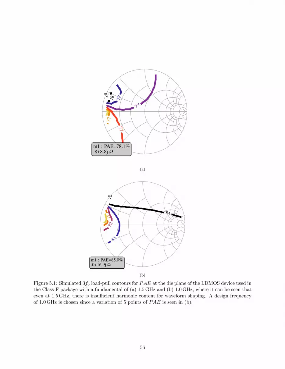
m1
m1 : PAE=78.1%.8+8.8j Ω
78 77
77
77
77
(a)
m1
m1 : PAE=85.0%.0+16.9j Ω
84
83
82
81
(b)
Figure 5.1: Simulated 3f0 load-pull contours for PAE at the die plane of the LDMOS device used inthe Class-F package with a fundamental of (a) 1.5 GHz and (b) 1.0 GHz, where it can be seen thateven at 1.5 GHz, there is insufficient harmonic content for waveform shaping. A design frequencyof 1.0 GHz is chosen since a variation of 5 points of PAE is seen in (b).
56

Ctab
Ctab
Die
C0
C1Cp1
L1
Ls1
Ls0
Lg
L0
(a)
Ctab
Ctab
C1C0
Die
Lg L0 L1
Cp1
Ls0 Ls1
2f0 3f0Cout
(b)
1.0 1.5 2.0 2.5 3.0 3.50.5 4.0
-50
-40
-30
-20
-10
-60
0
Frequency (GHz)
(c)
Figure 5.2: (a) Photo of the fabricated Class-F package design (which uses the standard packagein Fig. 4.2b which has a 280-mil wide tab), and (b) the equivalent circuit model (b), with elementvalues shown in Table 5.1. The 2f0 and 3f0 resonators are shown in the red and green boxes,respectively. Ls0 and Cp1 are designed to provide the phase transformation of the 3f0 short toan open at the virtual drain considering the device output capacitance (shown in grey). (c) Thesimulated return loss of each in-package resonator.
57

Table 5.1: Circuit model element values for Class-F Package
Ctab Lg L0 C0 Lls05.6 pF 1.43 nH 1.63 nH 4.01 pF 2.5 nH
Cp1 Ls1 L1 C1
21.29 pF 1.31 nH 1.53 nH 1.84 pF
the voltage at the virtual drain of the device. A short circuit is presented at even harmonics, while
an open circuit is presented at odd harmonics. In practice, a short at 2f0 and open at 3f0 is
sufficient, as the device gain drops significantly after the third harmonic. In a package, these
harmonic terminations are realized with lumped elements. An LC circuit consisting of a bond-wire
connected to a shunt MOS capacitor is placed in shunt immediately after the die to present a short
2f0, as shown in Fig. 5.2b. The elements L1 and C1 are chosen to resonate at 3f0 but require a
phase shift to be transformed to an open-circuit at the virtual drain. The combination of elements
Ls0 and Cp1, as well as Cout and the 2f0 resonator, serve as an impedance transformer for the 3f0
resonator.
The values for the resonator elements are chosen to maximize inductance while considering the
trade-offs between Q-factor, loss, and package and mechanical limitations as discussed in Chapter 4.
All of the elements contribute to the fundamental pre-match. With the desired ideal network known
(values shown in Table 5.1), the package network design procedure detailed in previous sections is
followed to produce the final package design shown in Fig. 5.2a. Fundamental load-pull is performed
on the Class-F package using passive Focus tuners. Power measurements are de-embedded to the
package plane. The resulting PAE contours are plotted in Fig. 5.3 showing a maximum PAE of
67 % and an output power of 12 W for an LDMO PA in a single 10 x 10 mm2 package.
5.2 Class-F−1 GaN Package
Gallium Nitride is a wide bandgap semiconductor (3.4 eV in GaN versus 1.1 eV in Silicon) and
operates at a high voltage. Typical drain supply voltages for high-power lower-frequency GaN
58

Figure 5.3: Class-F package load-pull contours of constant PAE and Pout measured and de-embedded to the package plane. Input power is constant at 22 dBm.
transistors are 50 V with breakdown in excess of 140 V. For higher frequency devices, the gate length
is reduced and as a consequence the operating voltage as well as the breakdown becomes smaller.
For example, the nominal operating voltage for 150-nm GaN-on-SiC is 28 V with a breakdown of
60 V. Therefore GaN devices favor voltage instead of current peaking, corresponding to a class-F−1
instead of class-F waveforms. In class-F−1 mode, even harmonics are reflected by an open-ciruit
impedance to achieve the voltage-peaking operation and the odd harmonic impedances are short-
circuited to achieve current squaring.
5.2.1 Design Methodology for GaN class-F−1 in a package
In order to achieve class-F−1 operation, we investigate the equivalent circuit shown in Fig. 5.4. The
Cout is the equivalent output capacitance of the transistor. The series resonances L2/C2 and L3/C3
are coupled through the series inductor Lx and together present the correct terminations to the
2nd and 3rd harmonics [70]. The input admittance Yin in the Laplace domain is given by:
Yin(s) = sCout +sC2(s
ω02
)2
+ 1
+1
sLx +1
gL + sCtab +sC3(s
ω03
)2
+ 1
(5.1)
where gL is the normalized load admittance connected in parallel to Ctab, and ω02 and ω03 are the
resonant frequencies for the L2/C2 and L3/C3 resonators respectively. For a class-F−1 termination,
59

we require that the admittance at the 3rd harmonic is infinite. Doing so to Equation 5.1, in phasor
form, yields
Yin(jω3) =∞ = jω3Cout +jω3C3(
jω3
ω03
)2
+ 1
+ Yrem (5.2)
where Yrem is the remainder of the third term in Equation 5.1. Therefore by choosing values for
the L3/C3 circuit is resonant at 3rd harmonic (ω03 = ω3), a short circuit will be presented to the
drain. This gives a required relationship between L3 and C3. The 2nd harmonic admittance is zero
(open circuit) resulting in the following equation for the input admittance at the virtual drain:
Yin(jω2) = 0 = jω2 (Cout + Ca)− j1
ω2Lx(5.3)
where
Ca =C3
1−(ω2
ω03
)2 (5.4)
From Equation 5.3, we see, interestingly, that the 2nd harmonic impedance depends on Lx, Cout,
and the 3f0 resonator. With the latter two values already determined, Lx is simply given by:
Lx =1
ω22(Cout + Ca)
(5.5)
The remaining undetermined components are used to present a complex fundamental match
determined by load-pull. In practice, the series inductance Lx can become large (e.g. 1.5 nH in the
case for class-F−1 terminations) and difficult to obtain with bond-wires. For a more practical im-
plementation, in an alternative circuit, the series inductor can be replaced by a T-circuit consisting
of two smaller valued series inductors with a shunt capacitor between them. These topologies are
used for obtaining initial values for the circuit elements for an in-package class-F−1 PA using a
GaN device.
60

Figure 5.4: Equivalent circuit for a class-F−1 in a package.
Figure 5.5: Layout of the 25-W Qorvo GaN die with gate and drain pads labeled. The die includes2 cells of 4 375-µm gate fingers, with gate bondpads to each cell. The gates of the cells also leadto additional, parallel bondpands connected by a 5 Ω TaN resistor. Courtesy of Qorvo.
5.2.2 Class-F−1 GaN PA Design
A harmonically-terminated transistor package will be demonstrated with a 25-W Qorvo GaN die
(Fig. 5.5) at the same frequency of the previous designs (2.6 GHz). The die includes 2 cells of 4
375-µm gate fingers, with gate bondpads to each cell. The gates of the cells also lead to additional,
parallel bondpands connected by a 5 Ω TaN resistor. A bias point of Vds = 50 V, Ids = 20 mA is
chosen since it is near cutoff and therefore will produce significant 2nd harmonic power. The Y -
parameter extraction method detailed in [71] is used to approximate the device non-linear output
capacitances Cout. The resulting value over swept Vgs is shown in Fig. 5.6.
Load-pull is performed on the device to determine the desired impedances to be presented by
61

Figure 5.6: The extracted output capacitance Cout with swept gate voltage. At the chosen biaspoint, Cout is approximated to be 0.41 pF. This is were the slope of Cout is the greatest, indicatinga large degree of non-linearty and therefore harmonic content.
the drain network. The non-linear circuit given by the manufacturer models only the transistor
(up to the gate and drain fingers). The gate and drain manifolds are simulated in Sonnet software,
a finite-element EM solver chosen since it was seen that, due to the electrically small geometry of
a transistor die, the ports in other solvers couple and present additional capacitances that are not
physical. Load-pull is then performed on the transistor model including the FEM simulations of
the drain pad. The resulting PAE contours at each harmonic are shown in Fig. 5.7.
The load-pull contours indicate that there is sufficient harmonic content for waveform shaping.
The 2f0 LP is performed with 3f0 terminated at 50 Ω. In Fig. 5.8, the 2f0 LP contours are de-
embedded beyond Cout to the virtual drain of the device. The de-embedded contours indicate that
the device prefers a 2nd harmonic open and therefore class-F−1 operation, as already argued is
the case for GaN transistors [72]. The commercial package of the previously used LDMOS device
(Fig. 3.7) is used in the following design, since it has a large cavity and therefore allows for a more
complex matching network. With a known Cout and Ctab, the methodology of the previous section
is utilized to solve for the remaining elements in the drain network for a class-F−1 solution. These
resultant values are given in Table 5.2.
The physical in-package realization of the circuit model network is shown in Fig. 5.9. The profile
62

m1
m1 : PAE=86.2%9.0+33.4j Ω 68
70
73
77
82
86
PAE(%)
(a)
54
60
66
72
78
84
PAE(%)
(b)
70.0
72.5
75.0
77.5
80.0
82.5
85.0
PAE(%)
(c)
Figure 5.7: The simulated PAE contours at the die reference plane for LP at (a) f0, (b) 2f0, and(c) 3f0.
63

54
60
66
72
78
84
PAE(%)
Figure 5.8: The 2f0 LP contours of constant PAE of Fig. 5.7b deembeded to the virtual drain,indicating that the device prefers a 2f0 open, with the cross symbol indicating the peak efficiencyimpedance.
Ctab L3 C3 Lx L2 C2
Synthesized 1.9 pF 0.27 nH 1.5 pF 0.84 nH 0.42 nH 2.4 pFCtab L3 C3 Lx L2 C2 Lx2 Cx
Adjusted 1.9 pF 0.32 nH 1.0 pF 0.76 nH 1.0 nH 1.0 pF 0.87 nH 3.0 pF
Table 5.2: Circuit model element values for the class-F−1 package output network, as determinedfrom Sec. 5.2.2 (synthesized) and as adjusted for practical implementation (adjusted).
in each bond-wire array is designed and simulated in HFSS in individual segments until it presents
the desired inductance, then tuned once placed in the package due to both the placement of the
bond-wire landing and the coupling between other elements. The finalized profiles also adhere to
those that can be constructed by bonding machines. For example, the bond-wires should be at
least 6 mils apart on each pad.
In the L3 bond-wire (responsible for the 3f0 short), each individual bond-wire has a different
profile considering the geometry of the die bond-pads, the placement of the Lx bond-wires, and
the placement of the C3 capacitor. The Lx2 bond-wires are angled to both reduce mutual coupling
(allowing a 3rd bond-wire) and to allow for a better current distribution on the tab and therefore
lower insertion loss [54].
The topology is revised from that of Fig. 5.4 in order to make the network symmetric, since
64

Figure 5.9: The physical realization of the drain network using package parasitics, device intrinsiccapacitance, bond-wires, and capacitors to present Class-F−1 impedances to the virtual drain.
it was found that symmetric current distributions throughout an in-package network results in
reduced insertion loss. Multiple bond-wires to minimize bond-wire loss at each node and also
betters current handling. However, this reduces total inductance requiring longer bond-wires and
relying on mutual inductance.
Even with multiple bond-wires at every node, the equivalent loss of each bond-wire array is
approximately 0.2 Ω. Although this is a relatively low resistance (made by intentionally using
multiple bond-wires), the impact on harmonic termination fidelity is significant. This is illustrated
in Fig. 5.10, where the left Smith chart shows the input impedance of the drain network with the
ideal lossless circuit model. The Smith chart in Fig. 5.10b shows the impact of an additional 0.2 Ω
resistance of the bond-wires. It is evident that the 2nd harmonic impedance is significantly reduced
in reflection coefficient magnitude which reduces efficiency by up to 10%. Although the same 0.2 Ω
loss was applied to each inductor in the circuit model, the loss had the most dramatic impact on
the 2nd harmonic termination. This is due to the impedance inverter formed by the Lx-Cx-Lx2
65

(a) (b)
Figure 5.10: (a) The input impedance of the drain network using the ideal, lossless circuit model.(b) The impedance presented by the device using the same circuit model but with an additional0.2 Ω reflecting the HFSS simulated drain network of Fig. 5.9. The markers m1, m7, and m5 indicatef0, 2f0, and 3f0 impedance, respectively.
.
network, as explained in Section 4.2.
has the most dramatic impact on the due to the impedance inverting network formed by Lx-
Cx-Lx2. considering the impedance inverter formed by the lx-cx-lx2 network.
This drain network is the result of iteration between the source network as well, since the design
of the gate network also affects allowable length of the series drain bond-wires and the placement of
L3/C3 resonator. The source network is a 2nd-order low-pass filter which matches to the complex
S11 of the device and is shown in Fig. 5.11 before the addition of the stability network.
5.2.3 In-package Stability
By matching a transistor within a package, before the PCB and bias network, the PA becomes
more prone to instability. Although an external stability network can be used to reduce gain at
low frequencies, unconditional stability is difficult to guarantee at the fundamental if the stability
network is introduced to an already matched PA. The criteria for stability used in this analysis is
a k-factor greater than 1 throughout the entire range of frequencies where the device has gain.
66

Figure 5.11: The physical realization of the gate network in HFSS (before the addition of thestability network) which matches to the complex input impedance of the device without the use ofan package-external matching network.
Without the presence of any stabilizing network, the device is prone to instability, as can be
seen in the plot of the k-factor of Fig. 5.12a when the device is input and output matched. The
commonly used technique of an input parallel RC network is then applied external to the package
(Fig. 5.12b) which satisfies the stabilty criteria for all but the range of frequencies near the design
frequency of the package. It was seen that no choice of R or C could increase the k-factor in this
frequency range without prohibitively reducing gain.
A package-internal stability network is added to affect the k-factor directly. The network is
restricted to small-valued, series inductance (bond-wire) and a shunt capacitance. In the presented
solution, the die on-chip resistor to a bond-pad is also used, creating a shunt RLC network to be
bonded to the gate offset gate pads of the die (Fig.5.5). Such a network eliminates the need for an
external network since, through the proper design of the elements, gain is reduced significantly at
low frequencies (less than 2 GHz) while gain is reduced at higher frequencies only enough to meet
the stability criteria. Shown in Fig. 5.12c is the circuit model and simulated k-factor of the package
design with the revised gate network.
67

(a)
(b)
(c)
Figure 5.12: The simulated k-factor (orange) and Gmax (blue) of the chosen GaN device over a widerange of frequencies for the scenario with (a) no stability network, (b) external stability networkconsisting of a parallel RC network (R = 20 Ω, C = 0.1 pF ), and (c) an internal stability network bya shunt RLC. In each case, the transistor is presented with the designed gate and drain matchingnetworks
.
68

(a)
(b)
Figure 5.13: The physical realization of the source network including internal stability network ofFig. 5.12c for 2 different manifistations of the drain network 3f0 resonator: (a) without adjustingthe drain network of Fig. 5.9 but with undesireable coupling between the gate and drain network,and (b) redesign of the 3f0 resonator with undesireable coupling of the resonator to the drainfundamental match.
.
69
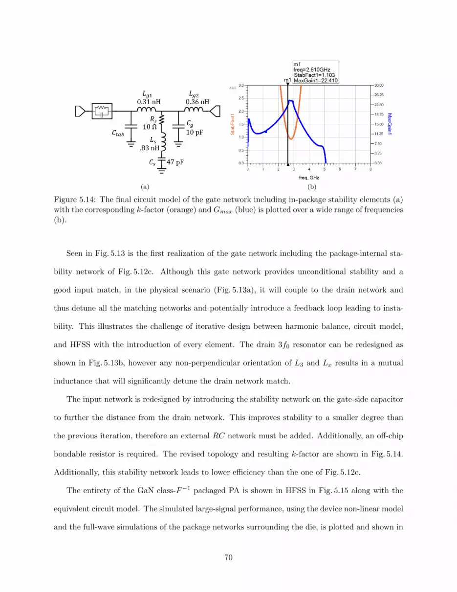
(a) (b)
Figure 5.14: The final circuit model of the gate network including in-package stability elements (a)with the corresponding k-factor (orange) and Gmax (blue) is plotted over a wide range of frequencies(b).
Seen in Fig. 5.13 is the first realization of the gate network including the package-internal sta-
bility network of Fig. 5.12c. Although this gate network provides unconditional stability and a
good input match, in the physical scenario (Fig. 5.13a), it will couple to the drain network and
thus detune all the matching networks and potentially introduce a feedback loop leading to insta-
bility. This illustrates the challenge of iterative design between harmonic balance, circuit model,
and HFSS with the introduction of every element. The drain 3f0 resonator can be redesigned as
shown in Fig. 5.13b, however any non-perpendicular orientation of L3 and Lx results in a mutual
inductance that will significantly detune the drain network match.
The input network is redesigned by introducing the stability network on the gate-side capacitor
to further the distance from the drain network. This improves stability to a smaller degree than
the previous iteration, therefore an external RC network must be added. Additionally, an off-chip
bondable resistor is required. The revised topology and resulting k-factor are shown in Fig. 5.14.
Additionally, this stability network leads to lower efficiency than the one of Fig. 5.12c.
The entirety of the GaN class-F−1 packaged PA is shown in HFSS in Fig. 5.15 along with the
equivalent circuit model. The simulated large-signal performance, using the device non-linear model
and the full-wave simulations of the package networks surrounding the die, is plotted and shown in
70

(a)
(b)
Figure 5.15: The entire Class-F−1 package design shown in HFSS (a) with equivalent circuit modelshown in (b).
71

Figure 5.16: Harmonic balance simulation using the HFSS-simulated S-parameters of the packagenetwork shown in Fig 5.15a and the non-linear model device. The input power is swept and thePAE (red), input power (pink) and transducer gain (blue) is plotted.
Fig. 5.16. At the time of writing, the package is being fabricated. Measurements are forthcoming.
5.3 Conclusion
Presented in this chapter is the design of two packages, each fully matched at the fundamental
frequency while also terminating the 2nd and 3rd harmonics in an open or short at the transistor
virtual drain. The first of the presented packages houses an LDMOS transistor, while the second
designed around a GaN HEMT. Although the LDMOS device prefers current peaking, while the
GaN device prefers voltage peaking, and therefore the circuits will differ, both designs require a
large degree of full-wave simulations, non-linear characterization, and design iterations.
It was seen that LDMOS is most efficient under class-F (current-peaking) conditions, which
greatly benefits from in-package designs since a 2f0 short-circuit impedance can be presented di-
recty at the output of the die by designing a bond-wire/capacitor shunt resonator on the die bond-
pad. However, LDMOS is ultimately limited in efficiency considering its large drain capacitance
(Cds=4.3 pF) and therefore limited output harmonic content.
The GaN device prefers a 2f0 open-circuit at the virtual drain corresponding to class-F−1,
72

which is difficult to achieve with in-package elements since highly-reflective impedances can only be
realized with low impedance circuits to ground. Large impedances with large reflection coefficients
therefore must be subject to the accumulated loss of the entire in-package network, making high-
fidelity open-circuit terminations difficult to achieve. Additionally, the larger fundamental output
impedance of GaN proved to be a challenge for this relatively low power level since it leads to the
need for larger series inductances (longer bond-wires). Interestingly, this is less of a challenge for
higher power devices since the output impedance will be lower.
In addition to demonstrating fully matched PAs within a package with small size and high
efficiency, a contribution of this chapter is a new type of in-package stability network which proved
to be effective in stabilizing a device that could not be stabilized with external stability networks.
73

6
Harmonic Injection
Contents
5.1 Class-F LDMOS Package . . . . . . . . . . . . . . . . . . . . . . . . . . . . . . . 55
5.2 Class-F−1 GaN Package . . . . . . . . . . . . . . . . . . . . . . . . . . . . . . . 58
5.3 Conclusion . . . . . . . . . . . . . . . . . . . . . . . . . . . . . . . . . . . . . . . . 72
As discussed in the previous chapters, to improve efficiency of microwave power amplifiers
(PAs), the active device is driven into saturation and the generated harmonics are reflected by the
output matching network in such a way that voltage and current waveforms are shaped for minimal
overlap during a period [73]. When sufficient harmonic content is available for waveform shaping,
the device is operated in a strongly non-linear regime and needs to be linearized for low-distortion
signal amplification [71]. Typically digital pre-distortion is required, adding complexity especially
for wideband signals. Harmonic injection (HI) at the input has also been investigated for improving
linearity for both tube [74] and solid-state [75] amplifiers. In [7], the phase and amplitude of the
2nd harmonic were chosen to optimize efficiency without regard for linearity. HI was also used to
improve linearity without regard for efficiency [76]. Both efficiency and linearity improvement of a
PA operating in CW mode are discussed in [77]. This improvement, however, is compared to a PA

f0
2f0
∆fZL
OMNIMN
2∆f
HI-PA
CarrierInjection
Pinj
Pin
Figure 6.1: Block diagram of the HI-PA. When driven into compression with a two-tone signal,the PA operates efficiently but not linearly. By injecting into the output a two-tone signal with adoubled carrier frequency (2f0) and tone spacing (2∆f), IMD3 can be reduced while maintainingefficiency through waveform shaping.
that does not include harmonic terminations.
To demonstrate the advantages of an HI-PA, this work directly compares PA performance with
passive and active 2nd harmonic terminations. A harmonically-terminated PA is designed to maxi-
mize power-added efficiency (PAE ) and then measured under load-side harmonic injection (Fig. 6.1)
to demonstrate an improvement in linearity while maintaining high efficiency. The phase and am-
plitude of the injected signal are dynamically adjusted during power sweeps showing reduction in
AM/AM distortion. With a two-tone input signal of varying separation, a reduction in third-order
intermodulation distortion (IMD3) by more than 10 dB is achieved while maintaining drain effi-
ciency ηD = 93% at peak power for the main PA. For this operating point, the total efficiency,
which includes the input powers at the fundamental and 2nd harmonic, is measured to be 80%.
6.1 HI-PA Design
The main PA at 2.2875 GHz is designed with a packaged Wolfspeed 10-W GaN HEMT CGH40010F.
We consider a 6-MHz signal bandwidth for the target application NASA’s S-Band Space Network
channel. The device is biased in Class AB (VDD = 28 V, IDQ = 67 mA) and the output matching
is designed as a trade-off between PAE and output power using load-pull. A 3-port injection
network is integrated into the HI-PA matching network to allow 2f0 injection without affecting f0
75

OMNIMN
Injection
Path
RF
In
Bias
tee
RF
Out
Fundamental
match
Figure 6.2: Photograph of the fabricated 2.3-GHz HI-PA on Rogers 4350B substrate and copperbaseplate. The board size is 106 mm × 76 mm.
impedance, Fig. 6.2. The PA was tested alone and with the 2f0 = 4.575 GHz injection path enabled
and the results compared in experiment.
6.1.1 Bias-tee Design
Considering the significant 2f0 content in the drain circuit, the bias network (Fig. 6.3) is designed
to have a high impedance at both f0 and 2f0. Furthermore, for minimal impact on the injected
signal, the impedance at 2f0 should be close to an open-circuit impedance. This is achieved by
choosing Lb to be the Coilcraft 0603CS 5.6 nH inductor considering that the parasitic capacitance
between the inductor windings in parallel with the self inductance resonates at 2f0. The simulated
impedance presented by the bias line to the RF path is shown in Fig. 6.4. Shunt capacitor Cb
with a series resonance at f0 serves to short any fundamental content beyond the RF choke. The
DC-RF isolation of the designed bias network, Fig. 6.3, is achieved through careful layout with
electromagnetic co-simulations.
The baseband impedance of the bias-tee must be as small as possible in order to minimize
memory effects induced by the bias line [78]. An inductor is used instead of a quarter wavelength
76

DC
RF
DC
RF
Figure 6.3: Isolation between the DC and the RF path from 0.5 to 10 GHz, showing a high bias-lineimpedance across a bandwidth of greater than 10 GHz (including up to 3f0).
line in order to increase the bandwidth of the bias tee, but the windings of the inductor will
increase resistance. However, since the self-resonance of an inductor is inversely proportional to
its self-inductance [79], the choice of a bias-line inductor with a resonant frequency at 2f0 leads
to fewer windings (lower baseband impedance) than the traditional approach of using an inductor
with an f0 resonance. Consider the bias tee in Fig. 6.3 where Lb has a parallel resonance of f0
instead of 2f0 by using a 27 nH inductor instead of a 5.6 nH inductor of the same Coilcraft series.
The baseband resistance of the bias line for this case is compared in Fig. 6.5 to the designed bias
line. In using the 2f0 resonant inductor, the baseband resistance remains below 0.2 Ω from DC to
up to 5 times the signal bandwidth. Although both choices of Lb lead to a high bias-line impedance
at the design frequency, the baseband characteristic of the designed bias-line is more desireable for
improved PA linearity performance.
6.1.2 Output Network Design
Simulated source-pull (SP) and load-pull (LP) are performed in Keysight ADS with the manufacturer-
provided nonlinear model. Since the bias network affects the fundamental impedance, a two-tone
10-MHz load-pull is performed with a reference plane located after the bias tee and the results for
PAE and IMD3 are shown in Fig. 6.6. The matching network is implemented on microstrip Rogers
4350B 30-mil substrate and the input is matched for gain.
77

2 f0
f0
Figure 6.4: The impedance presented by the bias line to the RF path, plotted from 2 to 10 GHz.The bias line is high-impedance over a large range of frequencies, with 2f0 near an open circuit.
20 40 60 80 100Frequency (MHz)
0.0
0.1
0.2
0.3
0.4
0.5
0.6
0.7
0.8
Bia
sL
ine
Res
ista
nce
(Ω)
Lb resonant at 2 f0
Lb resonant at f0
Figure 6.5: The baseband resistance of the bias-line for the case where Lb is parallel resonant atf0 (red) and 2f0 (yellow). Although both choices of Lb lead to a high bias-line impedance at thedesign frequency, the latter results in a bias-line that has a 2-3 times lower baseband impedancethan a traditionally designed bias-line.
78

0
10
20
30
40
50
60
PA
E(%
)
IMD
3(d
Bc)
18
16
14
12
10
Figure 6.6: Simulated 10-MHz spaced two-tone LP PAE and IMD3 contours at the reference planebetween the bias-tee and the PA output. The S11 of the EM-simualated matching network is alsoplotted from 1-8 GHz (gold dashed) with a marker (gold circle) at the design carrier frequency.
The 2f0 is injected through a diplexing network that presents an open at f0 and a passive 2f0
terminated at the device drain. The microstrip network together with an unloaded (open) SMA
connector is designed to terminate the 2nd harmonic in a high-efficiency region of the load-pull
contours. Therefore, by disconnecting the 2f0 injection source, a direct comparison can be made
between a PA with passive and active harmonic terminations. With 50 Ω connected to the injection
path, the 2nd harmonic is pre-matched to 47 Ω during 2f0 injection. The injection path includes a
DC block, and is meandered to fit the OMN within a 2”×3” form factor. The S -parameters of the
injection path are plotted in Fig. 6.8. A bandwidth-limiting factor for harmonic injection lies in the
bandwidth of the diplexor and therefore input and injected signal bandwidth must be considered
in the diplexor design. Additionally, it is desireable in terms of linearity that the diplexor presents
similar transmissive and reflective behavior across the entire bandwidth. The designed diplexor
provides reflection coeffecients of -25 dB across a 60 MHz bandwidth at each band (f0, 2f0, and
3f0).
The 2nd harmonic must be introduced as close to the device as possible to minimize injection
signal attenuation and therefore the required injected power. The simulated impedance of the
entire drain network under both conditions (loaded and unloaded injection port) is shown in Fig.
79

6.9, also showing the impedance at 2f0. The 3rd harmonic is terminated for peak efficiency and
the injection path does not affect its impedance.
Since the device is biased in a class-AB bias, significant 2f0 power will be generated. By
additionally injecting external harmonic power, an active impedance is synthesized at the 2nd
harmonic and therefore can present impedances outside of the unity radius Smith chart. In Keysight
ADS harmonic-balance, the 2f0 power and phase was swept. An ideal lossless directional coupler
is placed at the device output in order to sample seperately the 2f0 power from the device and
the injected 2f0 at the device plane. With the phase and amplitude of the generated and injected
harmonic sampled, the actively synthesized impedance can be determined. The ηtotal was then
simulated during the injection sweeps (assuming ηinj=50%) to produce the injection contours shown
in Fig. 6.7.
6.2 HI-PA Measurements
A setup based on two synchronized National Instruments VSTs is used to characterize the HI-PA.
An external RF source (HP 83650A) generates the f0 carrier, which is locked to the local oscillator
of a VST. The first VST is locked at 2f0 = 4.575 GHz, derived from f0 with a frequency multiplier
(Mini-Circuits ZX90-2-36+) and an high-pass filter (Mini-Circuits VHF-3800+). In this way, two
carriers, f0 and 2f0, are phase-coherent and phase-aligned. The RF generation and acquisition
(after calibrating the VSTs), are synchronized with a trigger and a 10 MHz reference clock. An
instrumentation driver (Mercury Systems SM0825-40) amplifies the f0 signal up to 29.5 dBm at
the PA input. The second signal at 2f0 is amplified by a bench-top driver (Keysight 83020A). The
measured CW performance with the injection port unloaded (passive 2f0 termination) is plotted
from 2 to 2.4 GHz in Fig. 6.10, demonstrating G = 12 dB, Pout = 41.5 dBm, and ηD = 72% at the
design frequency.
To account for the input DC power, as well as the powers at f0 and 2f0, we define a total
80

Figure 6.7: Simulated ηtotal contours (assuming ηinj=50%) constructed by sampling the forward andbackward 2f0 power at the device plane. The dotted lines indicate constant injected phase. Withno injection, the 2nd harmonic impedance assumes the passive 47 Ω passive pre-match impedance.
Figure 6.8: S-parameters of the injection path showing diplexing characteristic of the OMN. Theinjection path presents an open at f0 and 3f0, while presenting 50 Ω at 2f0.
81

PAE (%)
45
50
55
60
65
70
75
Figure 6.9: The 2f0 PAE contours are plotted with a continuous line (purple). The impedancepresented by the output network including the injection port SMA connector when the injectionport is unloaded (left) and loaded (right) is plotted from 2-8 GHz (gold, dashed trace), with Γ2f0
marked by a circle (purple).
Figure 6.10: Measured CW gain, POUT , and ηd of the PA. The efficiency of the PA is fine-tuned topeak at the targeted frequency f0 = 2.2875 GHz.
efficiency ηtotal as:
ηtotal =Pout(f0)
Pdc + Pinj/ηinj(6.1)
where Pinj is the injected 2f0 power and ηinj is the drain efficiency of the injection path active
components. With injection enabled, the measured ηtotal as a function of injected phase and
amplitude is shown in Fig. 6.11 for two values of injection-path efficiency: ηinj = 100% and 50%.
82

(a)
(b)
Figure 6.11: Measured contours of constant ηtotal assuming an injector efficiency of (a) 100% and(b) 50%, with swept injected phase and power at a fixed CW input signal at 30 dBm. Note thatlower injected power is necessary to reach the maximum ηtotal when considering a non-ideal 2f0injection.
For a 50 point reduction in ηinj , total efficiency reduces by seven points and the maximum ηtotal
contour is achieved at a lower Pinj . Additionally, the ηtotal contours can be related to Pout contours
plotted in Fig. 6.12 to show that 2f0 injection can also increase f0 output power by improving the
efficiency of the main PA.
Referring to Fig. 1, a two-tone signal at f0 with ∆f spacing is input to the PA, while a second
two-tone signal, centered at 2f0 and with 2∆f spacing, is concurrently injected at the HI port.
83

5 10 15 20 25 30Injected 2f0 Power (dBm)
0
50
100
150
200
250
300
350
Inje
cted
2f0
Phas
e(d
eg)
40.1
40.2
40.4
40.5
40.5
40.7
40.7
40.8 40.8
40.8
41.0
41.1
41.3
41.4
41.6
Pout (dBm)
Figure 6.12: Measured contours of constant Pout with swept injected phase and power at a fixed f0CW input signal at 30 dBm, showing injection can affect f0 output power by improving efficiency.
Figure 6.13: Measured modulated gain, drain and total efficiency of the amplifier at f0 with andwithout 2nd harmonic injection (open and 50 Ω load on the HI port). Both the main and injectedsignals are amplitude modulated. When HI is employed, the gain is flatter while the efficiency isalso improved as a result of waveform shaping with 2nd harmonic.
84

Figure 6.14: Normalized AM/AM characteristics of the PA with and without HI. The significantAM/AM distortion can be mitigated by 2nd harmonic injection. After HI, the residual distortionshows an odd-order nonlinearity that can be reduced with injection of higher order harmonics.
Figure 6.15: Normalized spectra showing a two-tone test at f0 with 10 MHz spacing andPOUT,MAX = 41.5 dBm. More than 10 dB improvement in the IMD3 is demonstrated by injectinga two-tone signal with 32 dBm power at 2f0 while the upper IMD5 is below 30 dBc.
85

In this case, both the main and injected signals are amplitude modulated with a 3-dB peak-to-
average ratio (PAR), resulting in higher efficiencies when compared to CW measurements because
of the lower PA temperatures. The large signal performance, with and without HI, is shown in
Fig. 6.13. With HI, gain is shown to be linearized with a maximum variation of ∼0.3 dB, while
ηD and ηtotal at higher output power also improve as a result of waveform shaping. Measurements
are also performed with the injection path unloaded, when it presents a passive 2f0 termination as
indicated by Fig. 6.9. Additionally, the PA is characterized for the case when the path is loaded with
50 Ω and presents near-50 Ω at 2f0 to the device. These two passive harmonic loading conditions
are compared directly to HI in Fig. 6.13.
6.3 Linearity Measurements
The HI-PA linearity is studied with the normalized AM/AM plot of Fig. 6.14. Here, the compressing
behavior of the PA is significantly reduced with HI as also visible in the residual AM/AM distortion.
Note that the injected signal at 2f0, identical to the signal at f0 but with twice the bandwidth,
reduces most of the compression, but injection of the 3rd harmonic is required to remove the residual
distortion. Linearity is also verified in the frequency domain, Fig. 6.15, where the IMD3 products
are reduced more than 10 dB while the IMD5 products remain below 35 dBc. Similar results are
obtained for tone spacing from 100 kHz up to 10 MHz.
6.4 Conclusion
A high-efficiency GaN PA is designed with harmonics terminated passively using traditional ele-
ments such as microstrip lines and stubs. An unloaded SMA connector at an edge of the PA board
is included in the design of the 2f0 impedance that is terminated in a high-efficiency region of the
Smith chart. The drain network is designed such that when the connector is loaded with a 50 Ω
system (e.g., another PA), the 2f0 impedance returns to near-50 Ω, serving as a 2f0 pre-match for
active impedance tuning. Under injection, an actively synthesized 2f0 impedance is presented to
86

the device. By designing the drain network to present either a passive or active 2f0 termination,
the advantages and disadvantages of an HI-PA can be directly observed.
Although the scope of this work does not include the design of the active components which
generate the 2f0 injection, the theoretical efficiency of this path is considered in the calculation of
the total HI-PA efficiency where it is seen that reducing ninj from 100% to 50% reduces ηtotal by
only 7 points while reducing the Pinj required for maximum ηtotal from 32 dBm to 29 dBm (3 dB
reduction).
With an active 2f0 termination, 2 dB greater gain and 3 points greater ηtotal are measured at
peak power, assuming ηinj = 50%. With a passive termination, the efficiency is greater at > 3 dB
backoff, however IMD3 is 10 dB greater. The AM/AM distortion is significantly reduced in the HI
case, and any further reduction in distortion would require injection of the 3rd harmonic in addition
to the 2nd. It has been shown that with harmonic injection, it is possible to achieve significantly
lower IMD3 and AM/AM distortion for a two-tone modulated signal while maintaining the high
efficiency of a harmonically-terminated PA. However, the ηinj = 50% assumption may be difficult
to achieve in practice considering that the injected power is at a doubled carrier frequency and
is comparable in power to the f0 output. Achieving a sufficiently high ηtotal would likely involve
careful co-design of the 2f0 injector and the rest of the transmitter, where frequency upconversion
and signal amplitude/phase control already occurs. Although this work provides insight into the
main PA performance, the feasibility of maintaining high system efficiency, particularly with carrier
frequencies beyond S-band, must be evaluated further.
87

7
Conclusions and Future Work
Contents
6.1 HI-PA Design . . . . . . . . . . . . . . . . . . . . . . . . . . . . . . . . . . . . . . 75
6.2 HI-PA Measurements . . . . . . . . . . . . . . . . . . . . . . . . . . . . . . . . . 80
6.3 Linearity Measurements . . . . . . . . . . . . . . . . . . . . . . . . . . . . . . . 86
6.4 Conclusion . . . . . . . . . . . . . . . . . . . . . . . . . . . . . . . . . . . . . . . . 86
7.1 Thesis Summary and Contributions
Microwave power amplifier efficiency is challenged by parasitic reactances and loss between the
design plane and the virtual drain, where theory for high-efficiency design is directly applied. The
efficiency of active devices is often limited by the packaging or interconnect from the device to the
rest of the system. In this work, the design plane is shifted closer to the virtual drain to enable
greater control of harmonic impedances. In Chapters 1-3, the active and passive networks between
the virtual drain and lead of a transistor package are modeled and characterized, including a
discussion of the limitations of commercial packages on efficiency. There is a general understanding
that packaged devices suffer from lower efficiency, but a comprehensive analysis can currently not

be found in the open literature. The goal of this thesis is to present methodology to any package
and transistor with a known geometry and non-linear model.
With the active and passive package environment modeled, considerations for the design of
in-package matching networks are explored in Chapter 4. A package design which allows greater
external harmonic control is presented along with active multi-harmonic load-pull. The contri-
butions of this work to in-package PA design are then described. Specifically, highly reflective
and precisely phased 2f0 impedances using in-package elements and parasitics are analyzed in the-
ory and demonstrated in measurement, and published in [56]. By doing so, an LDMOS PA with
package-internal matching is measured to have a state-of-the-art efficiency for an LDMOS-based
PA above 2.4 GHz.
Due to the small size of transistor packages, when designing in-package PAs, electromagnetic
coupling has a major effect and is difficult to fully take into account. Therefore there is a need to
measure and verfiy harmonic impedances presented to the drain of a die by in-package networks and
this work demonstrates a verification method in which the active device is replaced by a capacitor of
similar size and known value. S-parameter measurements of the fabricated purely passive package
can be directly compared to full-wave simulations up to the highest harmonic frequency and a
technique is published in [57] and [80]. This work was recognized by a Best Student Research
Paper award at IEEE WAMICON 2018.
A complete PA matching network including a complex fundamental match and 2nd and 3rd
harmonic terminations is fully realized with 3-dimensional elements and presented in Chapter 5
with both an LDMOS and GaN device without the need for external, PCB matching. A compact
LDMOS PA with in-package class-F impedances is demonstrated at 1 GHz with harmonic control
at 2 and 3 GHz at 10-W output power. This technique is extended by application to a 25-W GaN
device at 2.6 GHz where the increased harmonic control takes advantage of the greater harmonic
content of GaN devices. Both designs demonstrate for the first time control of up to 3 harmonics
within a package. By fully matching a transistor to up to its 3rd harmonic within a package, we
illuminate the need for an in-package stability network. A solution for stability using only bond-
89

wires, and bondable resistors and capacitors, is shown for the first time. This work is discussed
in [80].
This thesis also presents a PA design which allows the direct comparison of efficiency and
linearity performance of a packaged GaN device with passive and with active harmonic terminations.
The drain network integrates a diplexing network, a 3f0 termination, an f0 match and output port,
and a 2f0 input port. With 2f0 input port unloaded, the 2nd harmonic is passively terminated
in a high-PAE region of the unity Smith chart. When loaded, 50 Ω is presented to the device,
serving as a pre-match for the active impedance sweeps. The active terminations are achieved by
injection of an external source with doubled the carrier frequency and bandwidth. The injected
2nd achieves waveform shaping through active impedance synthesis while also reducing in-band
distortion products. Under injection, the PA was seen to have 10 dB lower IMD3 and reduced
AM-AM distortion while maintaing a similar total efficiency as in the passively-terminated mode.
The results of this work is published in [81].
Other contributions of this thesis include a series of non-standard multi-harmonic measurements.
Passive load-pull with harmonic terminations within the calibration standards was used for deter-
mining package limitations. Specialized active harmonic LP was applied validation of non-linear
models, and included the design bias networks within the calibration standards which presented
high impedances up to the highest harmonic. This was also applied to harmonic injection, which
can also be viewed as active LP at the 2nd harmonic. Then unique setup for harmonic injection was
developed with necessary phase alignment, phase-coherent doubled-frequency injection, including
basband and carrier frequenciy. In this experiment, the de-embedding of power and impedance
measuremetns of a drain network with 2 output ports was a key development in the design of a
harmonic injection PA.
The general microwave knowledge was related to other topics, including a dual-band high-
efficiency PA [82] , PAs for a multi-moded wireless powering cavity [83], and an efficient PA for
CubeSat transmitters [84].
90

7.2 Future Work
Ultimately the work presented in this thesis was on the intentional and precise design of bond-wires
and package parasitics at high frequencies, which has a wide variety of applications. Most active
devices require transition to PCB circuits.
It is of interest to apply in-package matching techniques to higher power applications. The
work presented scales well with output power in GaN since higher power devices have lower output
impedances, and since it was seen that packages present low impedance parasitics. It is easier for
the in-package network design to match the low impedance of the die to the low impedance of the
package. A smaller series inductance is required, which results in more practical bond-wires. This
was seen in practice in Chapter 5 where the series inductances necessary to achieve the fundamental
match for the LDMOS device was much smaller than those required to match the GaN device.
The scaling of this work to higher powers is further illustrated in Fig. 7.1. The drain network
can be modeled by a parallel shunt resistor Rp and capacitor Cp. Generally speaking, transistor
output power increases as the number and length of parallel gate/drain fingers increase, which
will in turn increase Cp and decrease Rp. Considering a typical power density of LDMOS devices,
the drain equivalent circuit with scaleable Rp and Cp is shown in Fig. 7.1. The scaling factor x is
swept and plotted. Package size also increases as output power increases (more parallel transistors,
larger peripharies) and therefore Ctab will also increase. As can be seen in this figure, the output
impedance of a transistor and the input impedance of simple in-package network converge to each
other in higher power scenarios.
The methodology of designing in-package networks is not restricted to matching networks of
single-ended amplifiers. The same principles may be used to explore using bond-wires and capacitors
to power combine multiple transistors within a package. This would be more advantageous that
doing so outside of the package since the transistors could be power-combined more directly, without
the loss of power or of impedance control as is seen with traditionally packaged devices. Similarly,
this work has plentiful applications in load-modulated PA topologies, such as outphasing or Doherty
91

Figure 7.1: A scalable circuit model of a transistor drain is shown in blue, with values fit froma typical power density of LDMOS devices. The output impedance of the model as the scalingfactor x is swept is plotted on the Smith chart in blue. This is related to the input impedance of aload-side package network, with Ctab increasing as package size increases.
PAs.
Many practical challenges were faced by using tradtional in-package elements. For example, an
inductance of 1.6 nH was needed in series for the design of the class-F package. This relatively high
inductance could only be realized with a single, large bond-wire, which in turn limited the current
handling capabilities of the PA. Seen in Fig. 7.2 was the result of a fused bond-wire during large-
signal operation. Another challenge is fabrication error. Shown in Fig. 7.4 is a scenario where there
was an error in the assembly drawing (Fig. 7.3) for the package design which led to a misplacement
of a capacitor in the low-pass filter match. With the series bond-wire Ls0 fixed in length by the
assembly drawing document, the loop height of the wire was lower than expected in simulation.
The inductance of Ls0 was 0.2 nH lower than desired, altough ultimately did not noticeably affect
the 1 GHz f0 match. Future work includes seeking elements alternative to bond-wires to realize
desired inductances.
92

Figure 7.2: Photo of a series bond-wire melted during large-signal operation due to the limitedcurrent handling capabilities of series bond-wire inductances of greater than approximately 1 nH.
In-package networks could be made even more effective using alternative in-package components.
The technique was limited by fact that bond-wires are small-valued inductances, non-rigid, and
relatively lossy, serving as low-Q inductors. An alternative to bond-wires with higher-Q, lower loss,
higher inductance could enable greater control of impedances within a package. A good solution
is seen in the new inductors becoming available from 3D Glass [85], which have high Q factors
since the inductors since the inductors are realized with thick copper lines placed on glass (Fig. 7.5)
and looped either in a single plane or 3-dimensionally. They also provide a much larger range of
inductances than can be realized with a bond-wire and are small enough to fit within a standard
transistor package.
Related to the active harmonic injection described in Chapter 6, basic signal performance was
demonstrated with a simple two-tone signal. Altough this is useful for quantifying linearity, in a real
application the baseband signal would need to be up-converted with a 2f0 LO and pre-processed
93

Figure 7.3: Assembly drawing of the Class-F design, with contradicting dimensions made by de-signer error leading to fabrication inconsistency with the initially simulated design.
Figure 7.4: The result of the assembly drawing error shown in Fig. 7.3, with (a) photograph of theassembled class-F package, (b) the intended design in HFSS, and (c) the HFSS image superimposedwith the fabricated package. The erroneous placement of a capacitor led to a lower bond-wire loopheight than expected and therefore a 0.2 nH lower inductance of the Ls0 inductor.
94

Figure 7.5: SEM of a planar spiral inductor from 3D Glass with a 50µ wide ccopper spiral supportedby 20 µ wide glass rails.
to take twice the bandwidth. Integration of circuitry that enables these functions along with a
2f0 driver in the injection path would be interesting avenues for future. Furthermore, redesign of
a harmonically-injected in a non-50 Ω to reduce the required injected power, thereby improving
ovreall efficiency.
95

Bibliography
[1] F. H. Raab, “Class-e, class-c, and class-f power amplifiers based upon a finite number of
harmonics,” IEEE Transactions on Microwave Theory and Techniques, vol. 49, no. 8, pp.
1462–1468, Aug 2001. x, 3, 18
[2] S. C. Cripps, RF Power Amplifiers for Wireless Communications, Second Edition (Artech
House Microwave Library (Hardcover)). Norwood, MA, USA: Artech House, Inc., 2006. 1, 3
[3] N. Ayllon, I. Davies, V. Valenta, and C. Boatella, “Making satellites reliable: The defini-
tion and design considerations of space-borne solid-state power amplifiers,” IEEE Microwave
Magazine, vol. 17, no. 9, pp. 24–31, Sept 2016. 1
[4] L. R. Kahn, “Single-sideband transmission by envelope elimination and restoration,” Proceed-
ings of the IRE, vol. 40, no. 7, pp. 803–806, July 1952. 3
[5] T. Barton and D. Perreault, “An rf-input outphasing power amplifier with rf signal decom-
position network,” in Microwave Symposium (IMS), 2015 IEEE MTT-S International, May
2015, pp. 1–4. 3
[6] H. Chireix, “High power outphasing modulation,” Proceedings of the Institute of Radio Engi-
neers, vol. 23, no. 11, pp. 1370–1392, Nov 1935. 3
[7] F. H. Raab, “Efficiency of doherty rf power-amplifier systems,” IEEE Transactions on Broad-
casting, vol. BC-33, no. 3, pp. 77–83, Sep. 1987. 3
96

[8] A. AlMuhaisen, P. Wright, J. Lees, P. J. Tasker, S. C. Cripps, and J. Benedikt, “Novel wide
band high-efficiency active harmonic injection power amplifier concept,” in Microwave Sym-
posium Digest (MTT), 2010 IEEE MTT-S International, May 2010, pp. 664–667. 3, 74
[9] F. H. Raab, P. Asbeck, S. Cripps, P. B. Kenington, Z. B. Popovic, N. Pothecary, J. F. Sevic,
and N. O. Sokal, “Power amplifiers and transmitters for rf and microwave,” IEEE Transactions
on Microwave Theory and Techniques, vol. 50, no. 3, pp. 814–826, Mar 2002. 3
[10] N. O. Sokal and A. D. Sokal, “Class e-a new class of high-efficiency tuned single-ended switching
power amplifiers,” IEEE Journal of Solid-State Circuits, vol. 10, no. 3, pp. 168–176, June 1975.
3
[11] K. Mimis, “Highly efficient, broadband and linear power amplifiers for base station applications
for 4g and beyond,” Ph.D. dissertation, University of Bristol, 2012. 4
[12] F. Lepine, A. Adahl, and H. Zirath, “A high efficient ldmos power amplifier based on an
inverse class f architecture,” in Microwave Conference, 2004. 34th European, vol. 3, Oct 2004,
pp. 1181–1184. 7
[13] Allam-ouyahia, C. Duperrier, C. Tolant, F. Temcamani, and P. Eudeline, “A 71.9% power-
added-efficiency inverse class-f ldmos,” in 2006 IEEE MTT-S International Microwave Sym-
posium Digest, June 2006, pp. 1542–1545. 7
[14] A. Adahl and H. Zirath, “An 1 ghz class e ldmos power amplifier,” in Microwave Conference,
2003 33rd European, Oct 2003, pp. 285–288. 7
[15] F. Lepine, R. Jos, and H. Zirath, “A load modulated high efficiency power amplifier,” in 2006
European Microwave Conference, Sept 2006, pp. 411–414. 7
[16] H. M. Nemati, C. Fager, and H. Zirath, “High efficiency ldmos current mode class-d power
amplifier at 1 ghz,” in 2006 European Microwave Conference, Sept 2006, pp. 176–179. 7
97

[17] P. Singerl, C. Fager, Z. Wang, C. Schuberth, and F. Dielacher, “A highly efficient 1-ghz, 15-w
power amplifier design based on a 50-v ldmos transistor,” in Microwave Symposium Digest
(MTT), 2010 IEEE MTT-S International, May 2010, pp. 1102–1105. 7
[18] H. M. Nemati, C. Fager, M. Thorsell, and H. Zirath, “High-efficiency ldmos power-amplifier
design at 1 ghz using an optimized transistor model,” IEEE Transactions on Microwave Theory
and Techniques, vol. 57, no. 7, pp. 1647–1654, July 2009. 7
[19] F. Lepine, A. Adahl, and H. Zirath, “L-band ldmos power amplifiers based on an inverse class-f
architecture,” IEEE Transactions on Microwave Theory and Techniques, vol. 53, no. 6, pp.
2007–2012, June 2005. 7
[20] A. Sheikh, C. Roff, J. Benedikt, P. Tasker, B. Noori, P. Aaen, and J. Wood, “Systematic
waveform engineering enabling high efficiency modes of operation in si ldmos at both l-band
and s-band frequencies,” in Microwave Symposium Digest, 2008 IEEE MTT-S International,
June 2008, pp. 1143–1146. 7
[21] M. S. Alavi, F. van Rijs, M. Marchetti, M. Squillante, T. Zhang, S. J. Theeuwen, Y. Volokhine,
R. H. Jos, M. P. van der Heijden, M. Acar, and L. C. de Vreede, “Efficient ldmos device oper-
ation for envelope tracking amplifiers through second harmonic manipulation,” in Microwave
Symposium Digest (MTT), 2011 IEEE MTT-S International, June 2011, pp. 1–1. 7
[22] Y.-S. Lee, K.-I. Jeon, and Y.-H. Jeong, “A 2.14 ghz class-e ldmos power amplifier,” in 2006
Asia-Pacific Microwave Conference, Dec 2006, pp. 1015–1018. 7
[23] H. Brech, W. Brakensiek, D. Burdeaux, W. Burger, C. Dragon, G. Formicone, B. Pryor,
and D. Rice, “Record efficiency and gain at 2.1 ghz of high power rf transistors for cellular
and 3g base stations,” in Electron Devices Meeting, 2003. IEDM ’03 Technical Digest. IEEE
International, Dec 2003, pp. 15.1.1–15.1.4. 7
98

[24] T. Yu and Z. Qiu, “S band broadband rf ldmos with excellent performance,” in Electron Devices
and Solid-State Circuits (EDSSC), 2013 IEEE International Conference of, June 2013, pp. 1–3.
7
[25] D. Gruner, R. Sorge, O. Bengtsson, and G. Boeck, “Cmos compatible medium voltage ldmos
transistors for wireless applications up to 5.8 ghz,” in Microwave Integrated Circuits Conference
(EuMIC), 2010 European, Sept 2010, pp. 146–149. 7
[26] G. Formicone, B. Battaglia, J. Burger, R. Keshishian, J. Titizian, and W. Veitschegger, “A
130w ldmos for 2.7-3.5 ghz broadband radar applications,” in Microwave Integrated Circuits
Conference (EuMIC), 2011 European, Oct 2011, pp. 220–223. 7
[27] C. Cassan and P. Gola, “A 3.5 ghz 25 w silicon ldmos rfic power amplifier for wimax applica-
tions,” in 2007 IEEE Radio Frequency Integrated Circuits (RFIC) Symposium, June 2007, pp.
87–90. 7
[28] P. Roblin, Nonlinear RF Circuits and Nonlinear Vector Network Analyzers: Interactive Mea-
surement and Design Techniques, ser. The Cambridge RF and Microwave Engineering Series.
Cambridge University Press, 2011. 6, 11, 20
[29] P. Aaen, J. A. Pla, and J. Wood, Modeling and Characterization of RF and Microwave
Power FETs. Cambridge University Press, 2007, see Passive part modeling section. [Online].
Available: http://dx.doi.org/10.1017/CBO9780511541124 10
[30] “Modelithics website,” www.modelithics.com. 10
[31] Nonlinear Transistor Model Parameter Extraction Techniques, ser. The Cambridge RF and
Microwave Engineering Series. Cambridge University Press, 2011. 11
[32] J. Hoversten, M. Roberg, and Z. Popovic, “Harmonic load pull of high-power microwave devices
using fundamental-only load pull tuners,” in Microwave Measurements Conference (ARFTG),
2010 75th ARFTG, May 2010, pp. 1–4. 20
99

[33] E. F. Calandra, “Measurement-based modeling of microwave transistor package and test-
fixture for device s-parameter deembedding,” in Proceedings of 1994 37th Midwest Symposium
on Circuits and Systems, vol. 2, Aug 1994, pp. 1227–1230 vol.2. 23
[34] T. Liang, J. Pla, P. Aaen, and M. Mahalingam, “Equivalent-circuit modeling and verification
of metal-ceramic packages for rf and microwave power transistors,” Microwave Theory and
Techniques, IEEE Transactions on, vol. 47, no. 6, pp. 709–714, Jun 1999. 23, 44
[35] T. Johansson and T. Arnborg, “A novel approach to 3-d modeling of packaged rf power tran-
sistors,” IEEE Transactions on Microwave Theory and Techniques, vol. 47, no. 6, pp. 760–768,
June 1999. 23
[36] K. Mouthaan, “Modeling of rf high power bipolar transistors,” Ph.D. dissertation, Delft Univ.
Technol., 2001. 23
[37] A. C. Polycarpou, P. A. Tirkas, and C. A. Balanis, “The finite-element method for modeling
circuits and interconnects for electronic packaging,” IEEE Transactions on Microwave Theory
and Techniques, vol. 45, no. 10, pp. 1868–1874, Oct 1997. 23, 24
[38] P. H. Aaen, J. A. Pla, and C. A. Balanis, “Modeling techniques suitable for cad-based design
of internal matching networks of high-power rf/microwave transistors,” IEEE Transactions on
Microwave Theory and Techniques, vol. 54, no. 7, pp. 3052–3059, July 2006. 24
[39] P. Aaen, J. Pla, and C. Balanis, “On the development of cad techniques suitable for the
design of high-power rf transistors,” Microwave Theory and Techniques, IEEE Transactions
on, vol. 53, no. 10, pp. 3067–3074, Oct 2005. 24
[40] I. J. Bahl, Lumped Elements for RF and Microwave Circuits. Artech House, 2003. 26, 27, 29
[41] J. M. El-Rashid, “Current distribution in high rf power transistors,” Ph.D. dissertation,
University of Gavle, September 2007. [Online]. Available: http://www.diva-portal.org/
smash/get/diva2:273582/FULLTEXT01.pdfTo 26
100

[42] R. E. Collin, Field Theory of Guided Waves. New York: McGraw-Hill, 1960, pp. 461–465,
470–474. 26
[43] F. Grover, Inductance Calculations: Working Formulas and Tables. Dover, New York, 1962.
26
[44] A. Ruehli, “Inductance calculations in a complex integrated circuit environment,” IBM Journal
of Research and Development, vol. 16, no. 5, pp. 470–481, Sept 1972. 26
[45] E. F. Kuester and D. Chang, “Propagating modes along a thin wire located above a grounded
dielectric slab,” Microwave Theory and Techniques, IEEE Transactions on, vol. 25, no. 12, pp.
1065–1069, Dec 1977. 26
[46] C. Holloway and E. F. Kuester, “Net and partial inductance of a microstrip ground plane,”
Electromagnetic Compatibility, IEEE Transactions on, vol. 40, no. 1, pp. 33–46, Feb 1998. 26
[47] F. Alimenti, U. Goebel, and R. Sorrentino, “Quasi static analysis of microstrip bondwire
interconnects,” in Microwave Symposium Digest, 1995., IEEE MTT-S International, May
1995, pp. 679–682 vol.2. 26
[48] R. Caverly, “Characteristic impedance of integrated circuit bond wires (short paper),” Mi-
crowave Theory and Techniques, IEEE Transactions on, vol. 34, no. 9, pp. 982–984, Sep 1986.
26
[49] C. Descharles, C. Algani, B. Mercier, and G. Alquie, “Physical and electrical modelling of
bonding wires up to 110 ghz,” in Microwave Conference, 2003. 33rd European, Oct 2003, pp.
639–642. 26
[50] F. Alimenti, P. Mezzanotte, L. Roselli, and R. Sorrentino, “Multi-wire microstrip interconnec-
tions: a systematic analysis for the extraction of an equivalent circuit,” in ARFTG Conference
Digest-Spring, 51st, vol. 33, June 1998, pp. 167–170. 26
101

[51] ——, “Modeling and characterization of the bonding-wire interconnection,” Microwave Theory
and Techniques, IEEE Transactions on, vol. 49, no. 1, pp. 142–150, Jan 2001. 26
[52] I. Doerr, L.-T. Hwang, G. Sommer, H. Oppermann, L. Li, M. Petras, S. Korf, F. Sahli, T. My-
ers, M. Miller, and W. John, “Parameterized models for a rf chip-to-substrate interconnect,”
in Electronic Components and Technology Conference, 2001. Proceedings., 51st, 2001, pp. 831–
838. 27
[53] A. Lu, W. Fan, L. Wai, L. Low, F. Ke, K. Yip, and Y. Lim, “Modeling and characterization of
wire bonding for rf applications,” in Electronic Components and Technology Conference, 2002.
Proceedings. 52nd, 2002, pp. 905–909. 27
[54] T. Ma, Y. Jiang, Y. Fan, X. Lin, and Z. Zhu, “A design of transition between microstrip line
and semiconductor devices with gold-bonding wire,” in Microwave, Antenna, Propagation,
and EMC Technologies for Wireless Communications (MAPE), 2011 IEEE 4th International
Symposium on, Nov 2011, pp. 303–305. 27, 64
[55] M. Roberg and Z. Popovic, “Analysis of high-efficiency power amplifiers with arbitrary output
harmonic terminations,” Microwave Theory and Techniques, IEEE Transactions on, vol. 59,
no. 8, pp. 2037–2048, Aug 2011. 39
[56] S. Rahimizadeh, J. Cheron, Q. Mu, and Z. Popovic, “In-package harmonic termination de-
sign for improving active device efficiency,” in 2016 IEEE MTT-S International Microwave
Symposium (IMS), May 2016, pp. 1–4. 51, 89
[57] S. Rahimizadeh and Z. Popovic, “In-package matching network validation for improving power
amplifier performance,” in 2018 IEEE 19th Wireless and Microwave Technology Conference
(WAMICON), April 2018, pp. 1–4. 51, 89
[58] H. Lee, H. Kang, W. Lim, W. Lee, J. Bae, and Y. Yang, “2.65 ghz 340 w dual internally
matched fets for compact doherty power amplifiers,” in 2018 IEEE Topical Conference on
102

RF/Microwave Power Amplifiers for Radio and Wireless Applications (PAWR), Jan 2018, pp.
43–46. 54, 55
[59] K. Oh, S. Lee, H. Kim, and H. Yoon, “An s-band internally matched packaged gan hemt
with over 720w peak power and 58% pae,” in 2018 IEEE/MTT-S International Microwave
Symposium - IMS, June 2018, pp. 643–646. 54
[60] E.-J. Lim, Y.-C. Rhee, and C.-S. Yoo, “High power, broadband class-j pa with internally pre-
matched fet,” in 2016 IEEE MTT-S International Microwave Symposium (IMS), May 2016,
pp. 1–3. 54
[61] K. Yamanaka, Y. Tuyama, H. Ohtsuka, S. Chaki, M. Nakayama, and Y. Hirano,
“Internally-matched gan hemt high efficiency power amplifier for space solar power stations,”
in 2010 Asia-Pacific Microwave Conference, Dec 2010, pp. 119–122. [Online]. Available:
https://ieeexplore.ieee.org/stamp/stamp.jsp?tp=&arnumber=5728605 54
[62] J. Cheron, M. Campovecchio, D. Barataud, T. Reveyrand, D. Floriot, M. Stanislawiak,
P. Eudeline, and W. Demenitroux, “Harmonic control in package of power gan
transistors for high efficiency and wideband performances in s-band,” in Microwave
Conference (EuMC), 2011 41st European, Oct 2011, pp. 1111–1114. [Online]. Available:
http://ieeexplore.ieee.org/stamp/stamp.jsp?tp=&arnumber=6102864&isnumber=6102757 54
[63] J. Cheron, M. Campovecchio, D. Barataud, T. Reveyrand, M. Stanislawiak, P. Eudeline, and
D. Floriot, “Wideband 50w packaged gan hemt with over 60pae through internal harmonic
control in s-band,” in Microwave Symposium Digest (MTT), 2012 IEEE MTT-S International,
June 2012, pp. 1–3. 54
[64] V. Carrubba, S. Maroldt, E. Ture, U. Udeh, M. Mußer, W. Bronner, R. Quay, and O. Am-
bacher, “Internally-packaged-matched continuous inverse class-fi wideband gan hpa,” in 2016
11th European Microwave Integrated Circuits Conference (EuMIC), Oct 2016, pp. 233–236. 54
103

[65] W. Lee, H. Lee, H. Kang, W. Lim, J. Han, K. C. Hwang, K. Lee, and Y. Yang, “X-band two-
stage doherty power amplifier based on pre-matched gan-hemts,” IET Microwaves, Antennas
Propagation, vol. 12, no. 2, pp. 179–184, 2018. 55
[66] M. P. van der Heijden, M. Acar, and S. Maroldt, “A package-integrated 50w high-efficiency rf
cmos-gan class-e power amplifier,” in 2013 IEEE MTT-S International Microwave Symposium
Digest (MTT), June 2013, pp. 1–3. 55
[67] D. Calvillo-Cortes, K. Shi, M. de Langen, F. van Rijs, and L. de Vreede, “On the design of
package-integrated rf high-power amplifiers,” in Microwave Symposium Digest (MTT), 2012
IEEE MTT-S International, June 2012, pp. 1–3. 55
[68] D. Calvillo-Cortes, M. van der Heijden, M. Acar, M. de Langen, R. Wesson, F. van Rijs, and
L. de Vreede, “A package-integrated chireix outphasing rf switch-mode high-power amplifier,”
Microwave Theory and Techniques, IEEE Transactions on, vol. 61, no. 10, pp. 3721–3732, Oct
2013. 55
[69] A. Sheikh, C. Roff, J. Benedikt, P. J. Tasker, B. Noori, J. Wood, and P. H. Aaen, “Peak class
f and inverse class f drain efficiencies using si ldmos in a limited bandwidth design,” IEEE
Microwave and Wireless Components Letters, vol. 19, no. 7, pp. 473–475, July 2009. 55
[70] P. de Paco, Private Communication, 2018. 59
[71] J. Vuolevi and T. Rahkonen, Distortion in RF Power Amplifiers. Artech House, 2003. 61, 74
[72] O. Kizilbey, “Highly efficient 2.7-2.9 ghz class-f and inverse class-f power amplifiers in gan
hemt technology,” IEICE Electronics Express, vol. 10, no. 7, Apr. 2013. 62
[73] P. J. Tasker, “Practical waveform engineering,” IEEE Microwave Magazine, vol. 10, no. 7, pp.
65–76, Dec 2009. 74
104

[74] M. Wirth, A. Singh, J. Scharer, and J. Booske, “Third-order intermodulation reduction by
harmonic injection in a twt amplifier,” IEEE Trans. on Electron Devices, vol. 49, no. 6, pp.
1082–1084, Jun 2002. 74
[75] D. P. Nguyen, T. Nguyen, and A. V. Pham, “Development of a highly linear ka-band power
amplifier using second harmonic injection linearization,” in 2016 46th European Microwave
Conference (EuMC), Oct 2016, pp. 835–838. 74
[76] S. Kusunoki, K. Kawakami, and T. Hatsugai, “Load-impedance and bias-network dependence
of power amplifier with second harmonic injection,” IEEE Trans. on Microwave Theory and
Techniques, vol. 52, no. 9, pp. 2169–2176, Sept 2004. 74
[77] A. Dani, M. Roberg, and Z. Popovic, “Pa efficiency and linearity enhancement using external
harmonic injection,” IEEE Trans. on Microwave Theory and Techniques, vol. 60, no. 12, pp.
4097–4106, Dec 2012. 74
[78] M. Franco, A. Guida, A. Katz, and P. Herczfeld, “Minimization of bias-induced memory effects
in uhf radio frequency high power amplifiers with broadband signals,” in 2007 IEEE Radio
and Wireless Symposium, Jan 2007, pp. 369–372. 76
[79] Coilcraft, “Measuring self-resonant frequency,” Tech. Rep., 2003. 77
[80] Z. P. S. Rahimizadeh, P. de Paco, “In package elements for harmonic control and stability,” in
IET Microwaves, Antennas & Propagation, 2019, in preperation for IEEE Transactions and
IET. 89, 90
[81] S. Rahimizadeh, T. Cappello, and Z. Popovic, “An efficient linear power amplifier with 2nd
harmonic injection,” in 2019 IEEE Topical Conference on RF/Microwave Power Amplifiers
for Radio and Wireless Applications (PAWR), 2019. 90
[82] A. Duh, S. Rahimizadeh, T. Barton, and Z. Popovic, “A 3.5/5.9-ghz dual-band output match-
ing network for an efficiency-optimized multiband power amplifier,” in 2018 IEEE Topical
105

Conference on RF/Microwave Power Amplifiers for Radio and Wireless Applications (PAWR),
Jan 2018, pp. 75–78, Winner of Best Student Reseach Paper Award. 90
[83] S. Rahimizadeh, S. Korhummel, B. Kaslon, and Z. Popovic, “Scalable adaptive wireless pow-
ering of multiple electronic devices in an over-moded cavity,” in 2013 IEEE Wireless Power
Transfer (WPT), May 2013, pp. 84–87. 90
[84] S. Rahimizadeh, P. Fetterer, Z. Popovic, and H. Shaw, “Improving cubesat transmitter eirp to
enable space network communication capabilities,” in URSI GASS, Montreal, Canada, 2017.
90
[85] “3d glass website,” www.3dglasssolutions.com. 93
106

Appendix A
Compact High-Gain CubeSat Antenna
The trend in increasing complexity and scope of CubeSat missions has driven a need for trans-
mitters that enable greater link distances, higher data-rates, and more sophisticated modulation
schemes. NASA’s Space Network and Deep Space Network provide the communication infrastruc-
ture necessary to satisfy this trend, however CubeSats currently lack the capabilities to utilize
this infrastructure. In order to enable CubeSat inclusion in space communication networks, this
chapter discusses a solution to increase the effective isotropic radiated power (EIRP) of a CubeSat
transmitter by way of increasing transmit antenna gain in a volume limited environment.
Maximizing antenna gain for CubeSats requires a large degree of innovation to depart from
current antenna solutions such as tape-measure dipoles and microstrip patches. In a collaborative
project between the University of Florida (UF), NASA Goddard Space Flight Center, and the
University of Colorado at Boulder, the proposed antenna seeks to achieve an aperture with a
diameter of 40 cm in order to sufficiently increase gain. This is large relative to the CubeSat,
which has dimensions of 30 x 30 x 40 cm3 (Fig A.1). In development by the UF collaborators is a
self-deployable reflector using shape-memory alloys and a copper-coated polymer mesh.
The link budget of the mission demanded that the antenna have greater than 15 dB of gain, an
RF bandwidth of 6 MHz. The antenna must also be circularly polarized according to the receiver

Figure A.1: The dimensions of the NASA CubeSat, with the reflector deployed (left) and stowed(right).
Figure A.2: Solidworks assembly of the initial backfire helix design with the curved mesh reflector.The reflector is 40 cm in diameter.
108

antennas in the Space Network.
Although the reflector is physically large, it is electrically small at the design frequency of
2.2875 GHz (corresponding to a diameter of approximately 3λ). Since traditional reflector-based
antennas require a diameter of at least 10λ, traditional feeds cannot be used. The reflector must
instead be treated as a curved ground plane placed in the feed near-field. Additionally, the feed
must be non-resonant since resonant feeds will be too large relative to the reflector.
A helix feed is chosen since it is compact, naturally circularly-polarized, collapseable/deployable,
and eliminates the need for a subreflector. The geometry of the initial design of the helix is shown
in Fig. A.2. By designing the helix to radiate in the backfire direction (Fig. A.3), the curved ground
plane can be used to further increase gain. This is illustrated in Fig. A.4 where the gain of the helix
is improved by 11.5 dB with the addition of the ground plane. The simulated radiation pattern of
the helix was intentionally designed to have a 13 dB edge taper, considering the reflector diameter
and the focal distance (10 cm).
The input impedance of the helix in Fig. A.2 is plotted in Fig. A.5 to show an inductive input
impedance. In order better match the antenna to 50 Ω, the characteristic impedance of the helix
was reduced by increasing the conductor width as shown in Fig. A.6. A width of 5 mm was chosen.
A.1 Feed Miniaturization
Although the specifications are met with the current design, it is desireable in this application to
further reduce the size of the antenna. This is achieved in simulation through dielectric loading
within the helix. The effective wavelength is reduced for higher permittivities, thereby reducing
the operating frequency of the antenna, as shown in Fig. A.7. By choosing Rogers RO3210 (εr =
10.2), an 84% reduction in volume is achieved with respect to the non-loaded helix, as illustrated in
Fig. A.8. This is used to obtain an 84% reduction in volume. However by doing so, the axial ratio
increased from 1.5 dB to 2.6 dB. Further work would be to improve the axial ratio of the loaded
helix by redesign of the helix and the shape of the dielectric. The final radiation pattern, with
109

Figure A.3: The electric field plotted in red and surface current density along the helix shown inblue for the initial design of the monofilar helix, showing radiation in the backfire direction.
curved ground plane present, is shown in Fig. A.9. The simulated gain in the endfire direction is
16.4 dB, which is a 16.4 dB improvement relative to traditional patch antennas used on CubeSats at
this frequency. On future CubeSats, this work provides a new type of compact, low-mass, antenna
with good directivity.
110

(a)
(b)
Figure A.4: HFSS-simulated gain pattern for the helix (a) without curved ground plane (reflector),and (b) with curved ground plane included. By designing the helix to radiate in the backfiredirection with 13 dB edge taper to the ground plane located 10 cm below the helix, the curvedground plane improves the gain by 11.5 dB.
111

Figure A.5: The simulated input impedance of the helix feed in Fig. A.2, with marker indicatingthe impedance at 2.2875 GHz.
Figure A.6: The reflection coefficient of the feed as the conductor width is stepped in size.
112

Figure A.7: The reflection coefficient of the feed as the conductor loading dielectric placed withinthe helix is increased in permittivity.
Figure A.8: The dielectric loaded helix compared to the unloaded helix, showing an 84% reductionin volume.
113

Figure A.9: HFSS simulated gain pattern (left) for the dielectrically-loaded backfire monofilar helixwith curved ground plane (right).
114


