Embed Size (px)
Citation preview
LDO
UVLOOTP
Delay
Match
HB
BST
VIN
EN
PWM
DHL DLH
6 ±�18 V
10 ±�60 V
HO
HS
5 VVDD
LO
VSS
Dead Time
Output
FilterMatching
Network
+
Vo(t)
-
VDD
CM Choke/
LFP
Envelope PWM of
base band signal
Digital
Isolator
ISO77xx
Switch node
Amplified Envelope voltage
of Base Band signal
LMG1210
1SNOAA44–December 2019Submit Documentation Feedback
Copyright © 2019, Texas Instruments Incorporated
LMG1210 Optimizing GaN RF Power Amplifiers
Application ReportSNOAA44–December 2019
LMG1210 Optimizing GaN RF Power Amplifiers
Jeffrey Mueller
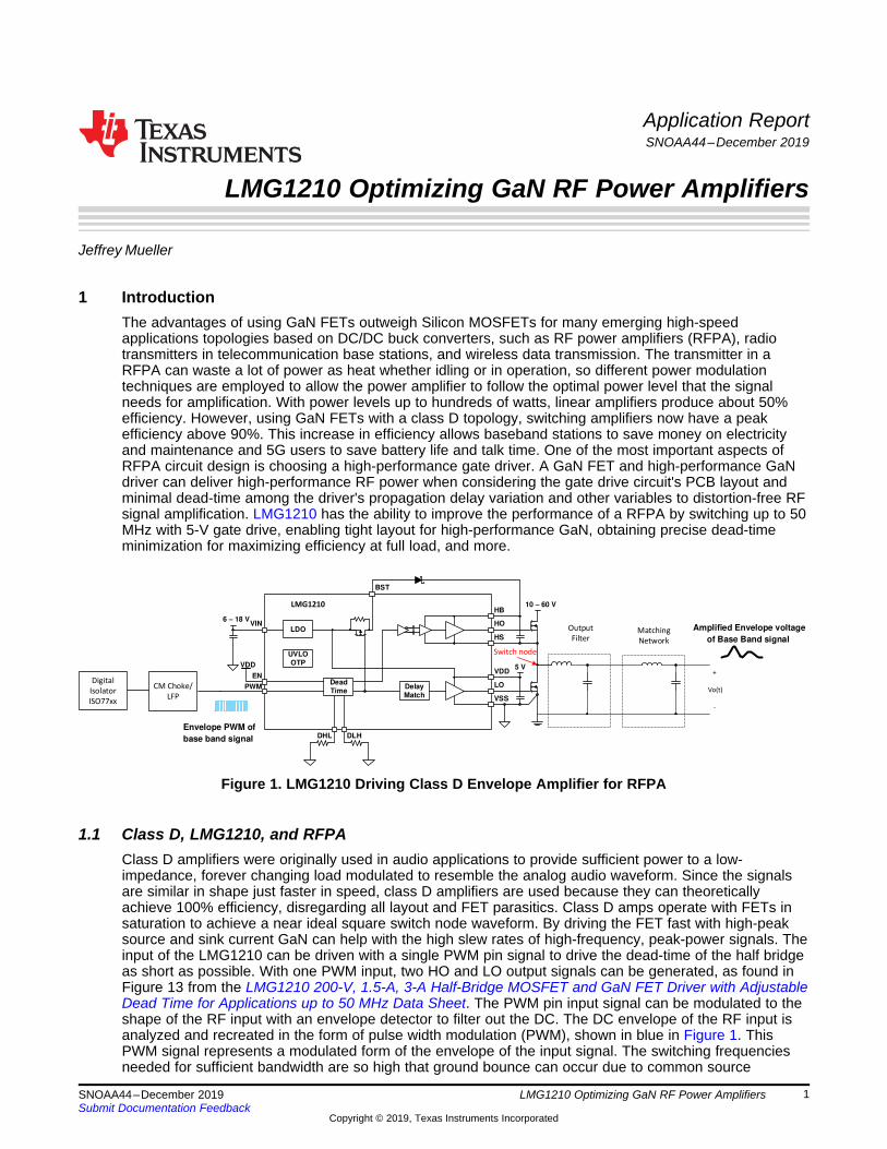
1 IntroductionThe advantages of using GaN FETs outweigh Silicon MOSFETs for many emerging high-speedapplications topologies based on DC/DC buck converters, such as RF power amplifiers (RFPA), radiotransmitters in telecommunication base stations, and wireless data transmission. The transmitter in aRFPA can waste a lot of power as heat whether idling or in operation, so different power modulationtechniques are employed to allow the power amplifier to follow the optimal power level that the signalneeds for amplification. With power levels up to hundreds of watts, linear amplifiers produce about 50%efficiency. However, using GaN FETs with a class D topology, switching amplifiers now have a peakefficiency above 90%. This increase in efficiency allows baseband stations to save money on electricityand maintenance and 5G users to save battery life and talk time. One of the most important aspects ofRFPA circuit design is choosing a high-performance gate driver. A GaN FET and high-performance GaNdriver can deliver high-performance RF power when considering the gate drive circuit's PCB layout andminimal dead-time among the driver's propagation delay variation and other variables to distortion-free RFsignal amplification. LMG1210 has the ability to improve the performance of a RFPA by switching up to 50MHz with 5-V gate drive, enabling tight layout for high-performance GaN, obtaining precise dead-timeminimization for maximizing efficiency at full load, and more.
Figure 1. LMG1210 Driving Class D Envelope Amplifier for RFPA
1.1 Class D, LMG1210, and RFPAClass D amplifiers were originally used in audio applications to provide sufficient power to a low-impedance, forever changing load modulated to resemble the analog audio waveform. Since the signalsare similar in shape just faster in speed, class D amplifiers are used because they can theoreticallyachieve 100% efficiency, disregarding all layout and FET parasitics. Class D amps operate with FETs insaturation to achieve a near ideal square switch node waveform. By driving the FET fast with high-peaksource and sink current GaN can help with the high slew rates of high-frequency, peak-power signals. Theinput of the LMG1210 can be driven with a single PWM pin signal to drive the dead-time of the half bridgeas short as possible. With one PWM input, two HO and LO output signals can be generated, as found inFigure 13 from the LMG1210 200-V, 1.5-A, 3-A Half-Bridge MOSFET and GaN FET Driver with AdjustableDead Time for Applications up to 50 MHz Data Sheet. The PWM pin input signal can be modulated to theshape of the RF input with an envelope detector to filter out the DC. The DC envelope of the RF input isanalyzed and recreated in the form of pulse width modulation (PWM), shown in blue in Figure 1. ThisPWM signal represents a modulated form of the envelope of the input signal. The switching frequenciesneeded for sufficient bandwidth are so high that ground bounce can occur due to common source
Envelope
Detection
20 - 60V
DC Supply
RF input
RF output
RF PA
Envelope Modulator
tracks envelope of
RF input for RFPA
drain bias supply
GND
Envelope
PA using
GND
Time
Vo
lta
ge
Time
Vo
lta
ge
Vo(t)
LMG1210
Introduction www.ti.com
2 SNOAA44–December 2019Submit Documentation Feedback
Copyright © 2019, Texas Instruments Incorporated
LMG1210 Optimizing GaN RF Power Amplifiers
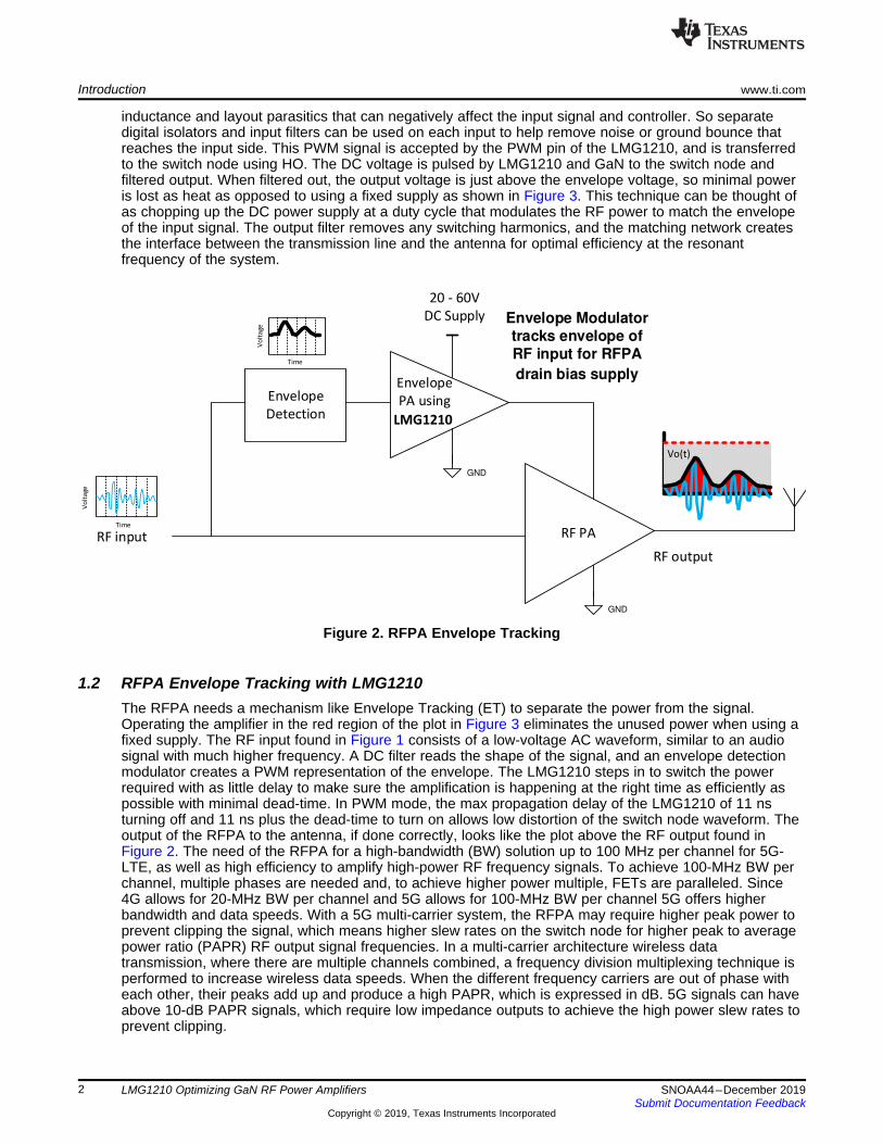
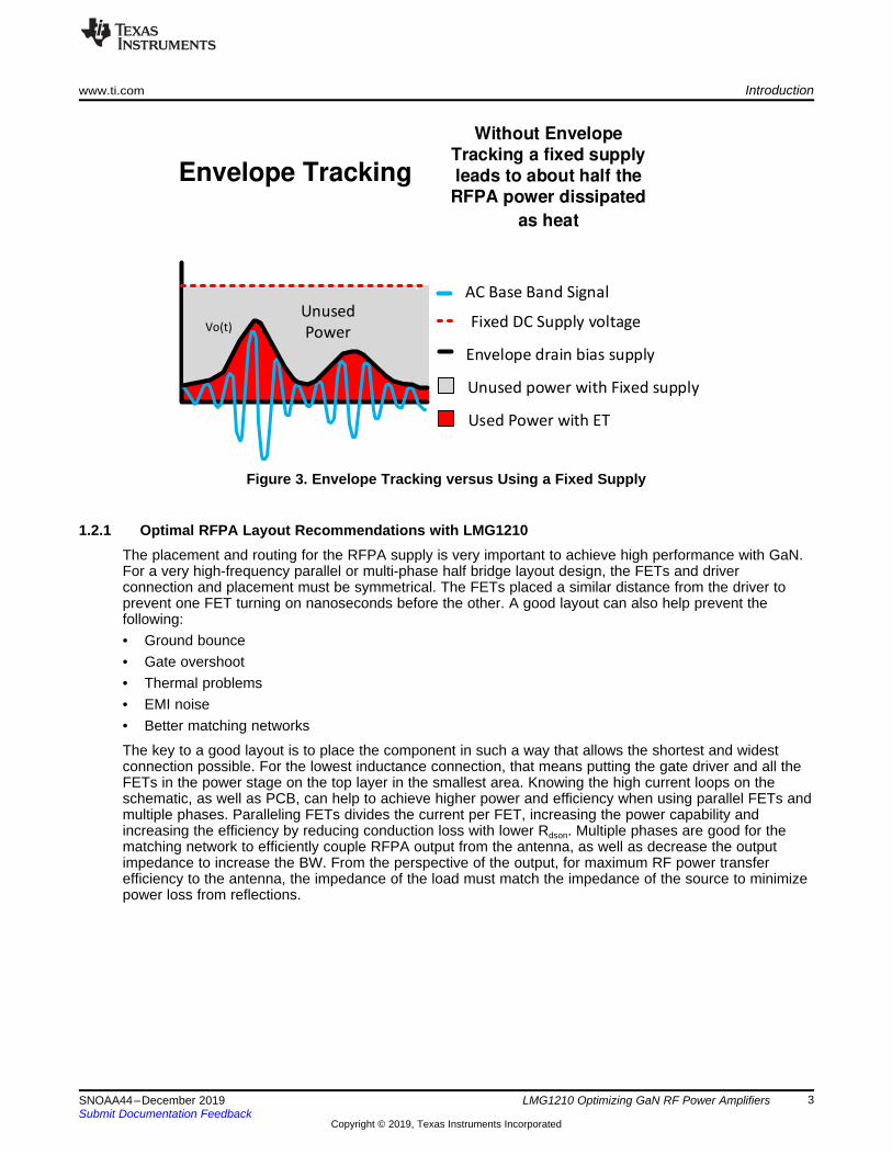
inductance and layout parasitics that can negatively affect the input signal and controller. So separatedigital isolators and input filters can be used on each input to help remove noise or ground bounce thatreaches the input side. This PWM signal is accepted by the PWM pin of the LMG1210, and is transferredto the switch node using HO. The DC voltage is pulsed by LMG1210 and GaN to the switch node andfiltered output. When filtered out, the output voltage is just above the envelope voltage, so minimal poweris lost as heat as opposed to using a fixed supply as shown in Figure 3. This technique can be thought ofas chopping up the DC power supply at a duty cycle that modulates the RF power to match the envelopeof the input signal. The output filter removes any switching harmonics, and the matching network createsthe interface between the transmission line and the antenna for optimal efficiency at the resonantfrequency of the system.
Figure 2. RFPA Envelope Tracking
1.2 RFPA Envelope Tracking with LMG1210The RFPA needs a mechanism like Envelope Tracking (ET) to separate the power from the signal.Operating the amplifier in the red region of the plot in Figure 3 eliminates the unused power when using afixed supply. The RF input found in Figure 1 consists of a low-voltage AC waveform, similar to an audiosignal with much higher frequency. A DC filter reads the shape of the signal, and an envelope detectionmodulator creates a PWM representation of the envelope. The LMG1210 steps in to switch the powerrequired with as little delay to make sure the amplification is happening at the right time as efficiently aspossible with minimal dead-time. In PWM mode, the max propagation delay of the LMG1210 of 11 nsturning off and 11 ns plus the dead-time to turn on allows low distortion of the switch node waveform. Theoutput of the RFPA to the antenna, if done correctly, looks like the plot above the RF output found inFigure 2. The need of the RFPA for a high-bandwidth (BW) solution up to 100 MHz per channel for 5G-LTE, as well as high efficiency to amplify high-power RF frequency signals. To achieve 100-MHz BW perchannel, multiple phases are needed and, to achieve higher power multiple, FETs are paralleled. Since4G allows for 20-MHz BW per channel and 5G allows for 100-MHz BW per channel 5G offers higherbandwidth and data speeds. With a 5G multi-carrier system, the RFPA may require higher peak power toprevent clipping the signal, which means higher slew rates on the switch node for higher peak to averagepower ratio (PAPR) RF output signal frequencies. In a multi-carrier architecture wireless datatransmission, where there are multiple channels combined, a frequency division multiplexing technique isperformed to increase wireless data speeds. When the different frequency carriers are out of phase witheach other, their peaks add up and produce a high PAPR, which is expressed in dB. 5G signals can haveabove 10-dB PAPR signals, which require low impedance outputs to achieve the high power slew rates toprevent clipping.
AC Base Band Signal
Envelope drain bias supply
Fixed DC Supply voltageUnused
Power
Unused power with Fixed supply
Used Power with ET
Vo(t)
Envelope Tracking
Without Envelope
Tracking a fixed supply
leads to about half the
RFPA power dissipated
as heat
www.ti.com Introduction
3SNOAA44–December 2019Submit Documentation Feedback
Copyright © 2019, Texas Instruments Incorporated
LMG1210 Optimizing GaN RF Power Amplifiers
Figure 3. Envelope Tracking versus Using a Fixed Supply
1.2.1 Optimal RFPA Layout Recommendations with LMG1210The placement and routing for the RFPA supply is very important to achieve high performance with GaN.For a very high-frequency parallel or multi-phase half bridge layout design, the FETs and driverconnection and placement must be symmetrical. The FETs placed a similar distance from the driver toprevent one FET turning on nanoseconds before the other. A good layout can also help prevent thefollowing:• Ground bounce• Gate overshoot• Thermal problems• EMI noise• Better matching networks
The key to a good layout is to place the component in such a way that allows the shortest and widestconnection possible. For the lowest inductance connection, that means putting the gate driver and all theFETs in the power stage on the top layer in the smallest area. Knowing the high current loops on theschematic, as well as PCB, can help to achieve higher power and efficiency when using parallel FETs andmultiple phases. Paralleling FETs divides the current per FET, increasing the power capability andincreasing the efficiency by reducing conduction loss with lower Rdson. Multiple phases are good for thematching network to efficiently couple RFPA output from the antenna, as well as decrease the outputimpedance to increase the BW. From the perspective of the output, for maximum RF power transferefficiency to the antenna, the impedance of the load must match the impedance of the source to minimizepower loss from reflections.
Dead Time Delay
Match
6 V to 18 V
LMG1210
VIN
EN
PWM
PWM input
BST
Dead time setupDHL DLH
HB
HO
HS
VDD
LO
VSS
5 V
VIN ( 0 ±�60V)
GaN HEMTsLDO
UVLO
OTP
VOUT
VDD
Bootstrap loop
Switch node return path
LO loop
HO loop
PGND to GND return path
Introduction www.ti.com
4 SNOAA44–December 2019Submit Documentation Feedback
Copyright © 2019, Texas Instruments Incorporated
LMG1210 Optimizing GaN RF Power Amplifiers
Figure 4. TIDA-01634 Essential Gate Loops Colored System Block Diagram
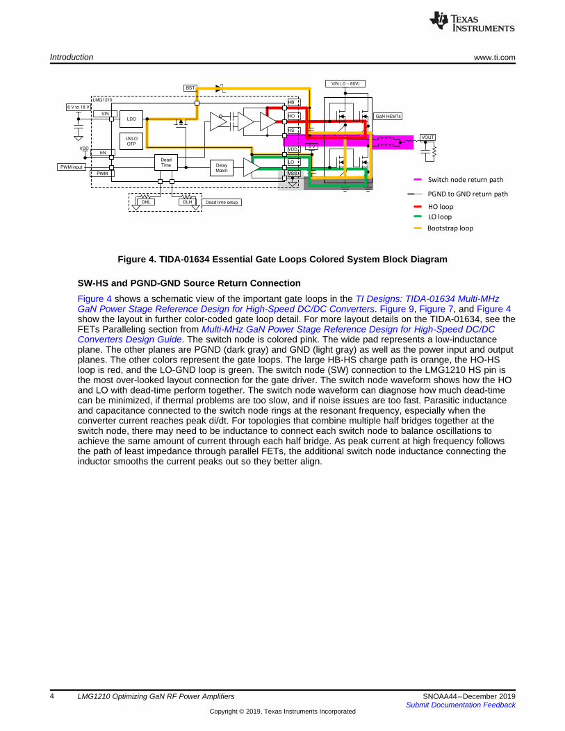
SW-HS and PGND-GND Source Return ConnectionFigure 4 shows a schematic view of the important gate loops in the TI Designs: TIDA-01634 Multi-MHzGaN Power Stage Reference Design for High-Speed DC/DC Converters. Figure 9, Figure 7, and Figure 4show the layout in further color-coded gate loop detail. For more layout details on the TIDA-01634, see theFETs Paralleling section from Multi-MHz GaN Power Stage Reference Design for High-Speed DC/DCConverters Design Guide. The switch node is colored pink. The wide pad represents a low-inductanceplane. The other planes are PGND (dark gray) and GND (light gray) as well as the power input and outputplanes. The other colors represent the gate loops. The large HB-HS charge path is orange, the HO-HSloop is red, and the LO-GND loop is green. The switch node (SW) connection to the LMG1210 HS pin isthe most over-looked layout connection for the gate driver. The switch node waveform shows how the HOand LO with dead-time perform together. The switch node waveform can diagnose how much dead-timecan be minimized, if thermal problems are too slow, and if noise issues are too fast. Parasitic inductanceand capacitance connected to the switch node rings at the resonant frequency, especially when theconverter current reaches peak di/dt. For topologies that combine multiple half bridges together at theswitch node, there may need to be inductance to connect each switch node to balance oscillations toachieve the same amount of current through each half bridge. As peak current at high frequency followsthe path of least impedance through parallel FETs, the additional switch node inductance connecting theinductor smooths the current peaks out so they better align.
Parallel source and return
loop cancel noise
HO-HS return path for HB#2
on 3rd
layer. VDD-GND return
path is for HB#1 on 2nd
layer.
www.ti.com Introduction
5SNOAA44–December 2019Submit Documentation Feedback
Copyright © 2019, Texas Instruments Incorporated
LMG1210 Optimizing GaN RF Power Amplifiers
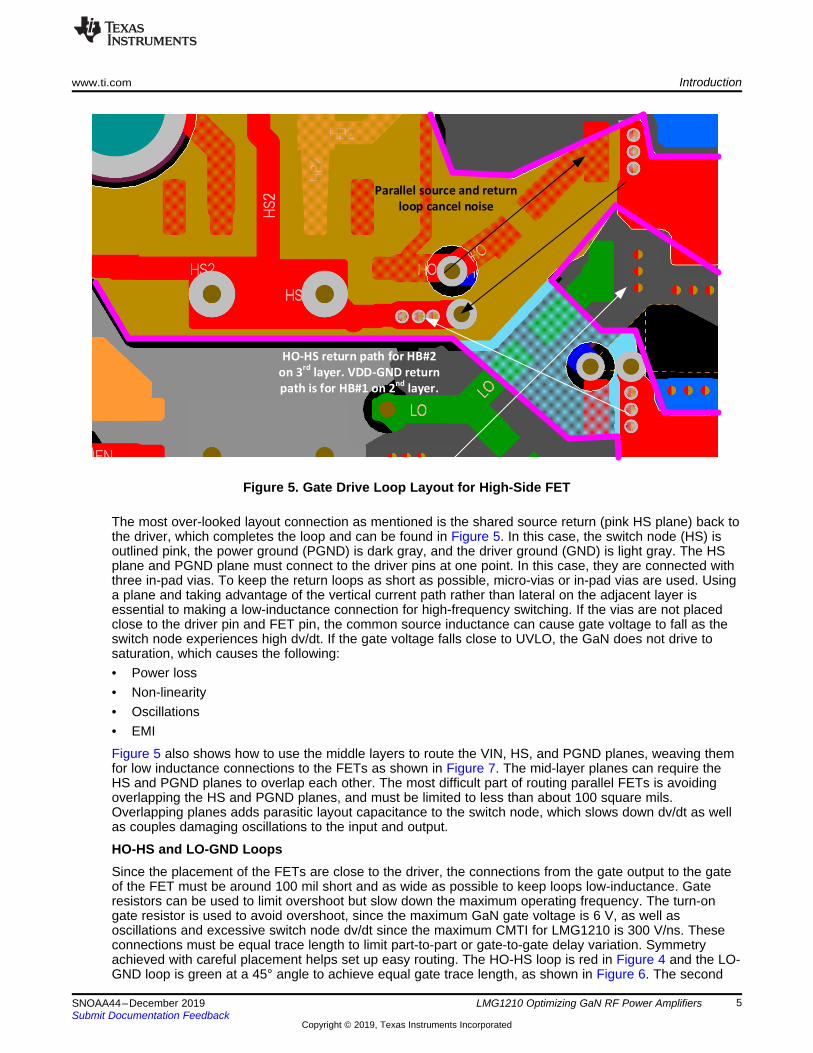
Figure 5. Gate Drive Loop Layout for High-Side FET
The most over-looked layout connection as mentioned is the shared source return (pink HS plane) back tothe driver, which completes the loop and can be found in Figure 5. In this case, the switch node (HS) isoutlined pink, the power ground (PGND) is dark gray, and the driver ground (GND) is light gray. The HSplane and PGND plane must connect to the driver pins at one point. In this case, they are connected withthree in-pad vias. To keep the return loops as short as possible, micro-vias or in-pad vias are used. Usinga plane and taking advantage of the vertical current path rather than lateral on the adjacent layer isessential to making a low-inductance connection for high-frequency switching. If the vias are not placedclose to the driver pin and FET pin, the common source inductance can cause gate voltage to fall as theswitch node experiences high dv/dt. If the gate voltage falls close to UVLO, the GaN does not drive tosaturation, which causes the following:• Power loss• Non-linearity• Oscillations• EMI
Figure 5 also shows how to use the middle layers to route the VIN, HS, and PGND planes, weaving themfor low inductance connections to the FETs as shown in Figure 7. The mid-layer planes can require theHS and PGND planes to overlap each other. The most difficult part of routing parallel FETs is avoidingoverlapping the HS and PGND planes, and must be limited to less than about 100 square mils.Overlapping planes adds parasitic layout capacitance to the switch node, which slows down dv/dt as wellas couples damaging oscillations to the input and output.
HO-HS and LO-GND LoopsSince the placement of the FETs are close to the driver, the connections from the gate output to the gateof the FET must be around 100 mil short and as wide as possible to keep loops low-inductance. Gateresistors can be used to limit overshoot but slow down the maximum operating frequency. The turn-ongate resistor is used to avoid overshoot, since the maximum GaN gate voltage is 6 V, as well asoscillations and excessive switch node dv/dt since the maximum CMTI for LMG1210 is 300 V/ns. Theseconnections must be equal trace length to limit part-to-part or gate-to-gate delay variation. Symmetryachieved with careful placement helps set up easy routing. The HO-HS loop is red in Figure 4 and the LO-GND loop is green at a 45° angle to achieve equal gate trace length, as shown in Figure 6. The second

Equal path length for HO-HS
(and LO-GND) source path
and return path.
Bootstrap cap
Microvias
Microvias
Microvias
Introduction www.ti.com
6 SNOAA44–December 2019Submit Documentation Feedback
Copyright © 2019, Texas Instruments Incorporated
LMG1210 Optimizing GaN RF Power Amplifiers
HO gate on the bottom half-bridge is routed on the bottom layer to keep equal gate lengths, as shown inFigure 6. In this case, the current flow on the input of FET gate is the opposite of the ground currentreturn, which offsets the magnetic field and reduces PCB stray inductance, as shown in Figure 5. FETselection is important to achieving a good gate loop. The output trace may need a via to reach the source.When using vias on the output gate loop, the vias must be placed as close to the output pin or as close tothe gate pad as possible to help avoid common source inductance in the gate loop. Although a two-layerboard can be used, a four-layer board helps with low-inductance, high-frequency performance. However,more layers can be added for paralleling more FETs or more phases.
Figure 6. Gate Drive Path for Paralleled FETs
VDD-GND and HB-HS Cap LoopsVDD and the bootstrap (HB-HS) cap placement are also important to achieving a tight gate loop since thehigh-peak source current of the driver is sourced from these caps. The VDD cap is light green and iscontained in the LO-GND green gate loop. It is highlighted as a reminder of this. The bootstrap HB nodeand the bootstrap charging path are orange, as seen in Figure 4. The placement of the VDD andbootstrap cap must be as close as possible to the pins. In this case, the VDD and HB cap are feedthroughcaps to further minimize the lead inductance and the overall loop inductance of the VDD-VSS and HB-HSgate loops. Place the VDD and HB-HS caps on top layer about 100 mil from the center of the thermal pad.The thermal pad and pinout of LMG1210 help route the gate loops with low inductance and allow a simpleconnection of the HS and VSS pins back to the thermal pad. The two separate thermal pads also allowthe lowest inductance connections for the source return path back to the driver. To minimize the gate loopinductance in the vertical z-direction and into the PCB board, use micro-vias to connect to the HS andGND plane on the adjacent layer. The LMG1210 has multiple HS pins to allow different HB cap placementand low-inductance connection to the FET source through an HS return plane.
LMG1210
Switch Node
Switch Node
Bootstrap
LO
HO
Switch Node
GND
Test
Point
VDD
www.ti.com Introduction
7SNOAA44–December 2019Submit Documentation Feedback
Copyright © 2019, Texas Instruments Incorporated
LMG1210 Optimizing GaN RF Power Amplifiers
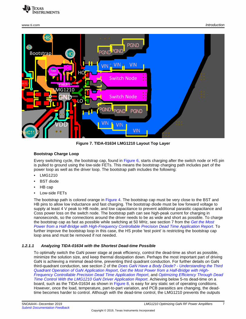
Figure 7. TIDA-01634 LMG1210 Layout Top Layer
Bootstrap Charge LoopEvery switching cycle, the bootstrap cap, found in Figure 6, starts charging after the switch node or HS pinis pulled to ground using the low-side FETs. This means the bootstrap charging path includes part of thepower loop as well as the driver loop. The bootstrap path includes the following:• LMG1210• BST diode• HB cap• Low-side FETs
The bootstrap path is colored orange in Figure 4. The bootstrap cap must be very close to the BST andHB pins to allow low inductance and fast charging. The bootstrap diode must be low forward voltage tosupply at least 4 V peak to HB node, and low capacitance to prevent additional parasitic capacitance andCoss power loss on the switch node. The bootstrap path can see high-peak current for charging innanoseconds, so the connections around the driver needs to be as wide and short as possible. To chargethe bootstrap cap as fast as possible while switching at 50 MHz, see section 7 from the Get the MostPower from a Half-Bridge with High-Frequency Controllable Precision Dead Time Application Report. Tofurther improve the bootstrap loop in this case, the HS probe 'test point' is restricting the bootstrap caploop area and must be removed if not needed.
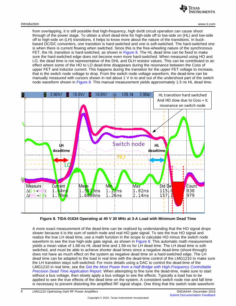
1.2.1.1 Analyzing TIDA-01634 with the Shortest Dead-time PossibleTo optimally switch the GaN power stage at peak efficiency, control the dead-time as short as possible,minimize the solution size, and keep thermal dissipation down. Perhaps the most important part of drivingGaN is achieving a minimal dead-time, preventing third quadrant conduction. For further details on GaNthird-quadrant conduction, see section 2 of the Does GaN Have a Body Diode? - Understanding the ThirdQuadrant Operation of GaN Application Report, Get the Most Power from a Half-Bridge with High-Frequency Controllable Precision Dead Time Application Report, and Optimizing Efficiency Through DeadTime Control With the LMG1210 GaN Driver Application Report. Achieving below 5-ns dead-time on aboard, such as the TIDA-01634 as shown in Figure 8, is easy for any static set of operating conditions.However, once the load, temperature, part-to-part variation, and PCB parasitics are changing, the dead-time becomes harder to control. Although with the dead-time control, the LMG1210 prevents the outputs
Switch node
HO
LO
HL
deadtime
LH
deadtime
HL transition hard switched
And HO slow due to Coss + IL
resonance on switch node
Introduction www.ti.com
8 SNOAA44–December 2019Submit Documentation Feedback
Copyright © 2019, Texas Instruments Incorporated
LMG1210 Optimizing GaN RF Power Amplifiers
from overlapping, it is still possible that high-frequency, high dv/dt circuit operation can cause shootthrough of the power stage. To obtain a short dead-time for high-side off to low-side on (HL) and low-sideoff to high-side on (LH) transitions, it helps to know more about the nature of the transitions. In buck-based DC/DC converters, one transition is hard-switched and one is soft-switched. The hard-switched oneis when there is current flowing when switched. Since this is the free-wheeling nature of the synchronousFET, the HL transition is hard-switched, as shown in Figure 8. The HL dead time can be fixed to makesure the hard-switched edge does not become even more hard-switched. When measured using HO andLO, the dead time is not representative of the DHL and DLH resistor values. This can be contributed to aneffect where some of the HO to LO dead-time disappears during the resonance between the Coss ofupper FET and inductor current. This happens during the transition for the upper FET voltage to increase,that is the switch node voltage to drop. From the switch node voltage waveform, the dead-time can bemanually measured with cursors shown in red about 1 V in to and out of the undershoot part of the switchnode waveform shown in Figure 8. This manual measurement yields approximately 1.5 ns HL dead time.
Figure 8. TIDA-01634 Operating at 40 V 30 MHz at 3-A Load with Minimum Dead Time
A more exact measurement of the dead-time can be realized by understanding that the HO signal dropsslower because it is the sum of switch node and real HO gate signal. To see the true HO signal andrealize the true LH dead time, use a math function in the scope to calculate HO minus the switch nodewaveform to see the true high-side gate signal, as shown in Figure 8. This automatic math measurementyields a mean value of 1.68-ns HL dead time and 1.56-ns for LH dead time. The LH dead time is soft-switched, and must be able to achieve shorter dead times since a negative dead-time (shoot-through)does not have as much effect on the system as negative dead time on a hard-switched edge. The LHdead time can be adapted to the load in real time with the dead-time control of the LMG1210 to make surethe LH transition stays soft-switched. For more details using a DAC to control the dead-time of theLMG1210 in real time, see the Get the Most Power from a Half-Bridge with High-Frequency ControllablePrecision Dead Time Application Report. When attempting to fine tune the dead-time, make sure to startwithout a bus voltage, then slowly apply a bus voltage to see the effects. Typically a load has to beapplied to see the true effects of the dead time on the system. A consistent switch node rise and fall timeis necessary to prevent distorting the amplified RF signal shape. One thing that the switch node waveform
Switch node
40V/ns
<500ps of
jitter
www.ti.com Summary
9SNOAA44–December 2019Submit Documentation Feedback
Copyright © 2019, Texas Instruments Incorporated
LMG1210 Optimizing GaN RF Power Amplifiers
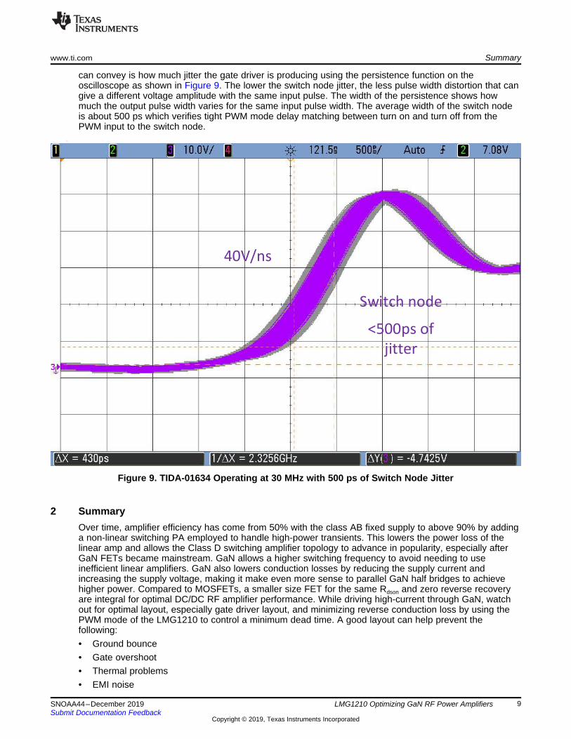
can convey is how much jitter the gate driver is producing using the persistence function on theoscilloscope as shown in Figure 9. The lower the switch node jitter, the less pulse width distortion that cangive a different voltage amplitude with the same input pulse. The width of the persistence shows howmuch the output pulse width varies for the same input pulse width. The average width of the switch nodeis about 500 ps which verifies tight PWM mode delay matching between turn on and turn off from thePWM input to the switch node.
Figure 9. TIDA-01634 Operating at 30 MHz with 500 ps of Switch Node Jitter
2 SummaryOver time, amplifier efficiency has come from 50% with the class AB fixed supply to above 90% by addinga non-linear switching PA employed to handle high-power transients. This lowers the power loss of thelinear amp and allows the Class D switching amplifier topology to advance in popularity, especially afterGaN FETs became mainstream. GaN allows a higher switching frequency to avoid needing to useinefficient linear amplifiers. GaN also lowers conduction losses by reducing the supply current andincreasing the supply voltage, making it make even more sense to parallel GaN half bridges to achievehigher power. Compared to MOSFETs, a smaller size FET for the same Rdson and zero reverse recoveryare integral for optimal DC/DC RF amplifier performance. While driving high-current through GaN, watchout for optimal layout, especially gate driver layout, and minimizing reverse conduction loss by using thePWM mode of the LMG1210 to control a minimum dead time. A good layout can help prevent thefollowing:• Ground bounce• Gate overshoot• Thermal problems• EMI noise
Related Documentation www.ti.com
10 SNOAA44–December 2019Submit Documentation Feedback
Copyright © 2019, Texas Instruments Incorporated
LMG1210 Optimizing GaN RF Power Amplifiers
• Better matching networks
The key to a good layout is to place the component in such a way that allows the shortest and widestconnection possible. Perhaps the most important part of driving GaN is achieving a minimal dead timepreventing third quadrant conduction. Achieving dead time below 5 ns on a board, such as the TIDA-01634, is easy, but high dv/dt circuit operation can still cause shoot-through. Following optimal layoutrecommendations from Section 3 and Section 1.2.1, as well as understanding how the dead-time ismeasured and fine tuned under high-frequency conditions found in Section 1.2.1.1, allows the bestperformance using the LMG1210 to drive a GaN Half Bridge for RF Power amplifiers.
3 Related Documentation• Texas Instruments, TIDA-01634 Multi-MHz GaN Power Stage Reference Design for High-Speed
DC/DC Converters Reference Design• Texas Instruments, LMG1210 200-V Half-Bridge MOSFET and GaN FET Driver Data Sheet• Texas Instruments, Using the LMG1210EVM-012 User's Guide• Texas Instruments, Design Considerations for LMG1205 GaN FET Driver for High-Frequency
Operation Application Report• Texas Instruments, Dead Time Optimization LMG1210 GaN Driver Application Report• Texas Instruments, Achieve Cooler Thermals and Less Power Loss of Your GaN Half-Bridge Design
with the LMG1210 Application Report• Texas Instruments, Does GaN Have a Body Diode? - Understanding the Third Quadrant Operation of
GaN Application Report• Texas Instruments, Get the Most Power from a Half-Bridge with High-Frequency Controllable Precision
Dead Time

IMPORTANT NOTICE AND DISCLAIMER
TI PROVIDES TECHNICAL AND RELIABILITY DATA (INCLUDING DATASHEETS), DESIGN RESOURCES (INCLUDING REFERENCEDESIGNS), APPLICATION OR OTHER DESIGN ADVICE, WEB TOOLS, SAFETY INFORMATION, AND OTHER RESOURCES “AS IS”AND WITH ALL FAULTS, AND DISCLAIMS ALL WARRANTIES, EXPRESS AND IMPLIED, INCLUDING WITHOUT LIMITATION ANYIMPLIED WARRANTIES OF MERCHANTABILITY, FITNESS FOR A PARTICULAR PURPOSE OR NON-INFRINGEMENT OF THIRDPARTY INTELLECTUAL PROPERTY RIGHTS.These resources are intended for skilled developers designing with TI products. You are solely responsible for (1) selecting the appropriateTI products for your application, (2) designing, validating and testing your application, and (3) ensuring your application meets applicablestandards, and any other safety, security, or other requirements. These resources are subject to change without notice. TI grants youpermission to use these resources only for development of an application that uses the TI products described in the resource. Otherreproduction and display of these resources is prohibited. No license is granted to any other TI intellectual property right or to any thirdparty intellectual property right. TI disclaims responsibility for, and you will fully indemnify TI and its representatives against, any claims,damages, costs, losses, and liabilities arising out of your use of these resources.TI’s products are provided subject to TI’s Terms of Sale (www.ti.com/legal/termsofsale.html) or other applicable terms available either onti.com or provided in conjunction with such TI products. TI’s provision of these resources does not expand or otherwise alter TI’s applicablewarranties or warranty disclaimers for TI products.
Mailing Address: Texas Instruments, Post Office Box 655303, Dallas, Texas 75265Copyright © 2019, Texas Instruments Incorporated


