Embed Size (px)
Citation preview
High Efficiency Si Integrated Micro-transformers Using Stacked Copper Windings for Power Conversion
Applications
Ningning Wang*, Santosh Kulkarni, Brice Jamieson,James Rohan, Declan Casey, Saibal Roy, Cian O’Mathuna Microsystems, Tyndall National Institute
University College Cork Cork, Ireland
Abstract— This paper details the design, fabrication, and characterization of silicon integrated micro-transformers. Two types of race-track shaped micro-transformers, single copper winding or single layer metal (SLM) and double copper winding or double layer metal (DLM) were designed and fabricated using standard CMOS processing. The DLM devices have higher inductance density than SLM devices realized within similar footprint area. The design study showed that the efficiency of micro-transformers increased from 37% for SLM designs to over 75% for DLM transformers at 20 MHz.
I. INTRODUCTION The ever shrinking size of handheld electronics has
highlighted the need for miniaturization of power converters. The overall size of converter can be reduced by increasing the converter switching frequency, because of reduction in required inductance value at higher frequencies which allows for smaller footprint of micro-transformers where isolation is preferred. Where only small inductance is required, the transformers can be potentially integrated onto the same substrate of power train to facilitate monolithic integration of power converter. However, to integrate micro-transformers on silicon and at the same time achieve higher efficiency at frequencies of 10s MHz, is still a very challenging task, due to increased winding losses in planar coils.
Much of the previous works have focused on the micro-fabrication and test of micro-transformers for isolation[1-7]. Solenoid type microtransformers are fabricated using multilevel metal schemes to wrap the coils around a magnetic core [1]–[4]. Single deposition of the magnetic core automatically provides a completely closed magnetic circuit, and hence minimizes leakage flux. However, the disadvantage of this approach is that it is difficult to introduce uniaxial anisotropy in the core, which is required for high frequency operation. An air-core microtransformer has also been implemented for signal and power transfer in [5,6], but restricted to operating at frequencies of several hundred MHz. The spiral type microtransformers which have a conductor
layer sandwiched between two layers of magnetic material, have also been reported by different research groups [7-9].
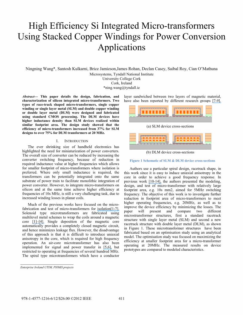
Figure 1 Schematic of SLM & DLM device cross-sections
Authors use a particular spiral design, racetrack shape, in this work since it is easy to induce uniaxial anisotropy in the core in order to achieve a good frequency response. In previous work [10-14], the authors presented the modeling, design, and test of micro-transformer with relatively large footprint area, e.g. 10s mm2, aimed for 5MHz switching frequency. The objective of this work is to investigate further reduction in footprint area of micro-transformers to meet higher operating frequencies, e.g. 20MHz, as well as to improve the device efficiency by minimizing the losses. The paper will present and compare two different microstransformer structures, first a standard racetrack structure with single layer metal (SLM) and second a new racetrack structure with double layer metal (DLM), as shown in Figure 1. These microtransformer structures have been fabricated based on an optimisation study using an analytical model. The optimisation study was focused on maximizing the efficiency at smaller footprint area for a micro-transformer operating at 20MHz. The measured results on device prototypes are compared to modeled characteristics.
Enterprise Ireland UTIM, PHMiS projects
(a) SLM device cross-sections
(b) DLM device cross-sections
978-1-4577-1216-6/12/$26.00 ©2012 IEEE 411

II. MICRO-TRANSFORMER DESIGN AND OPTIMISATION
Using the validated model introduced previously [12][13], a design optimization study was undertaken to investigate the impact of using new micro-transformer structures on the efficiency of a micro-transformer operating in a 20MHz converter. Three key parameters varied were (a) device footprint area (b) conductor width (c) moving from single metal layer (SLM) structure to double layer metal (DLM) structure in the analytical model for maximizing the efficiency. For both SLM and DLM transformer designs, the RMS value of the input sinusoidal voltage is fixed to 2.5V for a 40Ω resistive load. The relative permeability of the magnetic core material (Ni45Fe55) was taken to be 280 along with a material resistivity of 45 uΩ.cm. The spacing of the Cu conductors is fixed to 15 μm while the conductor width (Wp) was varied from 20 μm to 40 μm in the design study. For SLM designs, the thickness of Cu is fixed to 30 μm. The number of turns of primary and secondary is fixed to 5 turns. In the DLM designs, the thickness for each Cu layer is fixed to 15 μm . The number of turns of primary and secondary windings is fixed to 6 turns.
Figure 2 compares the efficiencies of different SLM & DLM designs with various footprint areas. SLM transformer designs, using smaller conductor width tend to have higher efficiency than the ones with larger conductor width, although smaller conductor width results in higher DC resistance. This is due to fact that wider conductor width will result in a shorter magnetic core and lower magnetizing inductance when the footprint area is restricted. The footprint area of a race-track micro-transformer is equal to the product of device length and device width. For a fixed number of turns of windings, wider conductor width leads to wider device width. A wider device width in turn reduces the length of device, which leads to shorter magnetic core length, and consequently higher magnetic flux density in the magnetic core. The eddy current loss and hysteresis loss increases with magnetic flux density. In addition to that, the lower magnetizing inductance give rises to higher magnetizing current and greater primary Cu conduction loss.
Figure 2 Modelled efficiency of transformers using single and
double layers of Cu windings.
In order to quantitatively illustrate the impact of conductor width and footprint area on the device efficiency, the loss breakdown of SLM transformer designs using 30 μm conductor width is shown in Figure 3. The calculated losses plotted in Figure 3 clearly show that the magnetic core loss is significantly higher than the Cu losses in all the designs. The magnetic core loss becomes less dominant with the increase of footprint area. This explains why the efficiency of a SLM micro-transformer is higher when using a smaller conductor width for a small footprint area. The efficiency of SLM designs can be improved by the increase of footprint area, because a larger footprint area leads to longer magnetic core, hence, smaller hysteresis and eddy current losses in the magnetic core, even though the secondary Cu loss is increased. The primary Cu loss is also reduced due to the smaller magnetizing current when the footprint area increases. The reduction of magnetic core losses will eventually be balanced by the increase of the Cu loss, so that it reaches an optimum footprint area to achieve the highest efficiency for the selected conductor width and number of turns.
Figure 3. Loss breakdown of SLM designs using 30μm
conductors
For a given small footprint area where the magnetic core losses dominate, smaller conductor width is preferred to achieve a better efficiency. The efficiency of SLM designs can be further increased by increasing conductor thickness and aspect ratio of spacing(the height of conductor spacing to the width of spacing). But, note that the optimized conductor thickness and aspect ratio of conductor spacing is set by the limitations in the MEMS processing technology. An alternative solution to addressing this limitation is to stack windings into two layers or multiple layers. The curves in Figure 2 clearly show the improvement in efficiency when using DLM structure. The conductor width varies in the same range as for the SLM designs, i.e. from 20μm to 40 μm. The predicted efficiency of DLM designs is substantially higher than that of SLM designs using a same conductor width and footprint area. It has been confirmed during the SLM design study that the dominant loss with a SLM device is magnetic core loss for a small footprint area. For a given area, if the number of turns of windings and conductor width are fixed,
0.00
0.02
0.04
0.06
0.08
0.10
0.12
0.14
0.16
1 2 3 4 5 6
Pow
er L
oss
(Wat
t)
Device Footprint Area (mm2)
Primary Cu lossSecondary Cu lossCore eddycurrent lossCore hysteresis lossTotal core lossTotal Cu loss
412

the resulting DLM device has a longer magnetic core than SLM device, hence less magnetic core loss. It explains why, for a small footprint area when the magnetic core losses dominate, the transformers using DLM structure show superior performance, especially for devices with footprint area of less than 4mm2. This advantage diminishes after the footprint area reaches to some extent. This is because when the footprint area becomes larger, e.g. larger than 3.5mm2, the reduction of magnetic core loss slows down while Cu loss still keeps increasing.
The loss mechanism within a DLM micro-transformer is the same as in a SLM device. The DLM designs using 20μm conductor width is chosen as an example to show the trade-off between different losses within a DLM micro-transformer when varying the footprint area. The detailed loss breakdown of DLM designs using 20μm conductor width is shown in Figure 4.
Figure 4. Loss breakdown of DLM designs using 20μm
conductors
As expected, the magnetic core loss dominates again for a small footprint area, e.g. <2.5mm2. This explains why using smaller conductor width achieves higher micro-transformer efficiency for a small footprint area, e.g. <2.5mm2. As for the same reason, For a fixed number of turns of windings and conductor width, a larger footprint area leads to longer magnetic core. A longer magnetic core means lower magnetic flux density in the core, which in turn reduces the eddy current loss and hysteresis loss. Because the number of turns of windings and width of conductor is fixed, the increase of footprint area also results in higher winding resistance. It reaches an optimum footprint area, where the increase of Cu loss can no longer compensated by the reduction of magnetic core. The efficiency of DLM design reaches its optimum at this optimum footprint area. In this design study, the optimum footprint area for 20μm conductor width is approx. 3.5mm2. The optimum footprint area becomes larger if using wider conductor width.
Based on the design study, the optimized design specifications for SLM and DLM microtransformers are summarized in Table below. Table 1. Specifications of the micro-inductors fabricated.
III. DEVICE FABRICATION
Figure 5 Fabrication process flow for DLM micro-transformers
Transformer Prototype SLM DLM Winding width, μm 40 40 Winding thickness, μm 30 15 Winding spacing, μm 20 15 Turns ratio, 4:4 6:6 Core thickness, μm 4.5 4.5 Core length, μm 1.09 1.32 Device length, mm 2.59 2.6 Device width, mm 1.35 1.15 DC resistance, Ohm 0.34 1.1 Inductance at 20MHz, nH 80 240
0
0.005
0.01
0.015
0.02
0.025
0.03
0.035
0.04
0.045
1 2 3 4 5 6
Pow
er L
oss
(Wat
t)
Device Footprint Area (mm2)
Core eddy current lossCore hysteresis lossSecondary Cu lossPrimary Cu lossTotal core lossTotal Cu loss
413

The fabrication process for DLM microtransformers is detailed in Figure 5. The fabrication for SLM micro-transformers is a 5 mask process using standard MEMS processing techniques, while fabrication process of DLM micro-transformer included two extra mask levels. The fabrication process for SLM microtransformers is similar to the process reported in our previous work [10]. Figure 6 shows the top view and cross-section of a micro-fabricated SLM transformer. The fabricated micro-transformer consists of a racetrack shaped copper winding (30 μm thick) sandwiched between two Ni45Fe55 magnetic cores (~4.5 μm thick). The bottom magnetic core is electroplated and patterned on native oxide insulated silicon wafer. The copper windings are electroplated on a patterned BCB (Benzocyclobutane, 13 μm thick) which insulates the windings from the bottom core. The top magnetic core is deposited and patterned using the same electroplating process as bottom core, on a patterned Su-8 (epoxy type photoresist, 50 μm thick) insulating the top core from windings.
The top view and cross-section of the DLM micro-transformers are shown in Figure 7. It is a 7 mask process having similar processing steps for the bottom core and bottom insulation. The copper windings, however are a 2 layered with Su-8 as insulating layer in-between. Each of the windings are 15 μm thick are electrodeposited with first layer deposited on BCB and second layer on Su-8 (20 μm thick). Su-8 (50 μm thick) is patterned on the second copper coil for top core insulation. The top magnetic core (4.5 μm thick) is electrodeposited and patterned on the Su-8 layer (similar to SLM).
(a)
(b)
Figure 6 (a) the resultant top view and (b)cross section of a prototype single metal layer
(a)
(b)
Figure 7 (a) resultant top view and (b) cross-section of a prototype double metal device
IV. DEVICE CHARACERISATION The fabricated micro-transformers were wire bonded to a
testing board. A de-embeding method is applied in this work to eliminate the series parasitic parasitics associated with the test-structure of the device under test (DUT) [13][15]. The wire-bonded devices were then was tested using a R&S Vector Network Analyzers ZRVE, which offers a testing frequency from 9KHz up to 4GHz. The measured two-port S parameters of DUT and the dummy device are transformed into impedance matrixes ZDUT and ZDummy, respectively. The de-embedding correction was performed by subtracting the impedance matrix of dummy device from that of DUT to obtain the impedance matrix of the micro-transformer tested.
The open circuit inductance and resistance of tested transformers can be obtained from Z11, the open circuit input impedance. Since the transformer has the same number of turns for primary and secondary, the open circuit inductance and resistance will be identical for both primary and secondary in each case. The measured open circuit inductance, Loc, and open circuit resistance, Roc, for both micro-transformers are shown in Figure 8. The Loc are approximately 85nH, and 210nH at 20MHz, for SLM and DLM, respectively. For both cases, the inductance holds up to at least 20MHz with less than 15% drop of inductance, although inductance drop is larger than expected.
414

Figure 8. Measured open circuit inductance and resistance
The DC resistance was tested using Kelvin 4-probe method. The measured primary and secondary DC resistances for SLM device are both 0.367Ω. Similarly, the primary and secondary DC resistances for DLM device are 1.096 Ω, and 0.962Ω, respectively. The measured resistance match well with the design values.
The measured voltage gain of the DUT under 50 Ω resistive load condition is plotted in Figure 9.
Figure 9. Measured voltage gain for SLM and DLM
As shown in Figure 9, both micro-transformers exhibit a high voltage gain of approx. –1dB at between 10MHz and 30 MHz. The low voltage gain at low frequencies is due to the low magnetizing inductance. The voltage gain starts to fall off at high frequencies because the eddy current loss increases significantly. The leakage inductance for SLM device and DLM device is estimated to be 6nH, 7.3nH. Based on the leakage inductance and magnetizing inductance, the DLM device is supposed to give better coupling. However, this is not reflected by the voltage gain measurement. The SLM device shows better voltage gain than DLM device. This is mainly because the impact of large resistance relative to their reactive impedances.
V. CONCLUSIONS The recent developments in the power electronics industry
have suggested that the future of power delivery for microprocessors and other portable/hand-held electronics will focus heavily on the development of miniaturised, high frequency power conversion modules. This paper presents the development of a thin film, magnetics-on-silicon technology platform that would deliver highly efficient micro-transformers capable of operating at 20 MHz. Two different structures of micro-transformers were investigated and compared. The measured DC resistance and inductance closely match the design values. The measured voltage gain for both transformers is approx. -1dB at between 10MHz and 30MHz, which indicates good coupling. According to the design study, an efficiency of up to 75% for DLM device can be expected when operating at 20MHz.
ACKNOWLEDGMENT The authors would like to acknowledge funding support
from Enterprise Ireland under CFTD 2008/331 Grant for the work described here.
REFERENCES [1] H. Kurata, K. Shirakawa, O. Nakazima, and K. Murakami, “Study of
Thin Film Micro Transformer with High Operating Frequency and Coupling Coeeficient”, IEEE Transactions on Magnetics, vol. 29, no. 6, pp. 3204–3206, Nov. 1993.
[2] M. Mino, T. Yachi, A. Tago, K. Yanagisawa, and K. Sakakibara, “Planar Microtransformer With Monolithically Integrated Rectifier Diodes For Micro-Switching Converters”, IEEE Trans. Magn., vol. 32, no. 2, pp. 291–296, Mar. 1996.
[3] M. Xu, T. M. Liakopoulos, and C. H. Ahn, “Packaging-compatible microinductors and microtransformers with screen-printed ferrite using low temperature processes”, IEEE Trans. Magn., vol. 34, no. 4, pp. 1369–1371, Jul. 1998.
[4] J. Y. Park and J. U. Bu, “Packaging Compatible Microtransformers on a Silicon Substrate”, IEEE Trans. Adv. Packag., vol. 26, no. 2, pp. 160–164, May 2003.
[5] Online,http://www.analog.com/Analog_Root/static/pdf/isolators/techDocs/isoPower.pdf, Analog Device.
[6] C. D. Meyer, S. S. Bedair, B. C. Morgan, and D. P. Arnold, “High-Inductance-Density, Air-Core, Power Inductors, and Transformers Designed for Operation at 100–500 MHz”, IEEE Transaction on Magnetics, Vol. 46, No. 6, June 2010.
[7] K. Yamaguchi, S. Ohnuma, T. Imagawa, J. Toriu, H. Matsuki, and K.Murakami, “Characteristics of a thin film microtransformer with circular spiral coils”,IEEE Trans. Magn., vol. 29, no. 5, pp. 2232–2237, Sep.1993.
[8] A. Lotfi, R. Bruce, V. Dover, L. Schneemeyer, and M. Steigerwald, “Micro-Transformer Devices Using Thin-Film Electiroplated Deposition”, in Proc. 29th IEEE Annu. Power Electronics Specialists Conf., PESC’98, Fukuoka, Japan, May 1998, vol. 2, pp. 1511–1515.
[9] C. R. Sullivan and S. R. Sanders, “Measured Performance of a High-Power-Density Microfabricated Transformer in a DC-DC Converter”, in Proc. IEEE Annu. Power Electronic Specialists Conf., PESC’96, Baveno, Italy, Jun. 1996, pp. 287–294.
[10] M. Brunet, T. O’Donnell, L. Baud, N. Wang, J. O’Brien, P. McCloskey, and S. C. O’Mathuna, “Performance of Micro-Transformers for DC-DC Converter Applications”, IEEE Trans. Magn., vol. 38, no. 5, pp. 3174–3176, Sep. 2002.
[11] N. Wang, T. O’Donnell, H. Hauser, P. McCloskey, S.C.O’Mathuna, “Hysteresis Modelling of High Frequency Micro-Transformers”, Journal of Magnetism and Magnetic Materials, Vol. 272-276, Supplement 1, May 2004, pp. E1763-E1764.
0
50
100
150
200
250
300
350
0
50
100
150
200
250
300
1.00E+06 1.00E+07 1.00E+08
Rin
( O
hm)
Lin
(nH
)
Frequency (Hz)
Loc_SLM Loc_DLM Roc_SLM Roc_DLM
-10
-9
-8
-7
-6
-5
-4
-3
-2
-1
0
1.0E+05 1.0E+06 1.0E+07 1.0E+08 1.0E+09
Volta
ge G
ain
(dB
)
Frequency (Hz)
DLM_50 Ohm load
SLM_50 Ohm load
415

[12] N. Wang, H. Hauser, T. O’Donnell, P. McCloskey, C.O’Mathuna, “Modelling of High Frequency Micro-Transformers”, IEEE Trans. On Magnetics, Vol. 40, No. 4, July 2004, pp 2014-2016.
[13] N. Wang, T. O’Donnell, S. Roy, S. Kulkarni, P. Mccloskey, and C. O’Mathuna “Thin Film Microtransformer Integrated on Silicon for Signal Isolation”, IEEE Transactions on Magnetics, Vol. 43, No. 6, June 2007
[14] T. O’Donnell et al., “Microfabricated inductors for 20 MHz DC-DC converters,” in Proc. APEC, 2008, pp. 689–693.
[15] Paul J. van Wijnen, On the Characterization and Optimisation of High-Speed Silicon Bipolar Transistors, Cascade Microtech, INC.
416


