Embed Size (px)
Citation preview

Research ArticleHigh-Efficient Circuits for Ternary Addition
Reza Faghih Mirzaee,1 Keivan Navi,2 and Nader Bagherzadeh3
1 Department of Computer Engineering, Islamic Azad University, Shahr-e-Qods Branch, Tehran 37541-374, Iran2 Faculty of Electrical and Computer Engineering, Shahid Beheshti University, G.C., Tehran 1983963113, Iran3Department of Electrical and Computer Engineering, Center for Pervasive Communications and Computing (CPCC),University of California, Irvine, CA 92697, USA
Correspondence should be addressed to Reza Faghih Mirzaee; [email protected]
Received 12 May 2014; Revised 3 August 2014; Accepted 9 August 2014; Published 1 September 2014
Academic Editor: Mohamed Masmoudi
Copyright © 2014 Reza Faghih Mirzaee et al. This is an open access article distributed under the Creative Commons AttributionLicense, which permits unrestricted use, distribution, and reproduction in any medium, provided the original work is properlycited.
New ternary adders, which are fundamental components of ternary addition, are presented in this paper. They are on the basisof a logic style which mostly generates binary signals. Therefore, static power dissipation reaches its minimum extent. Extensivedifferent analyses are carried out to examine how efficient the new designs are. For instance, the ternary ripple adder constructed bythe proposed ternary half and full adders consumes 2.33 𝜇W less power than the one implemented by the previous adder cells. It isalmost twice faster as well. Due to their unique superior characteristics for ternary circuitry, carbon nanotube field-effect transistorsare used to form the novel circuits, which are entirely suitable for practical applications.
1. Introduction
On-chip interconnections have become a serious challengeas more and more modules are packed into a chip. Theydissipate lots of energy, increase response time, and causecoupling effects by adding more capacitance, resistance, andinductance to a circuit [1]. Multiple-valued logic (MVL) is analternative solution to interconnect complexity and growingpower dissipated by wires [2]. It reduces the amount of wiresinside and outside a chip dramatically as more complexdesigns require a large number of wires for connecting circuitcomponents. In addition, MVL has the high potential forincreasing computational speed, reducing switching activity,and implementing many arithmetic and logic functions in asingle chip [2, 3]. Among many MVL systems, ternary logic(also known as three-valued logic) has soared in popularitydue to its simplicity and efficiency [4, 5].
In spite of potential superiorities of ternary logic, binary isstill the dominant logic for circuit design in the industry. Oneof the main reasons is the intrinsic behaviour of transistors.The on-off characteristic of a transistor makes it an idealdevice to implement Boolean algebra. However, dualismdoes not correspond to real-world applications effectively.
Another reason why ternary logic is not as popular as itsbinary counterpart is mainly because of the lack of sufficientpractical, high-performance logic gates and computationalcomponents. To make ternary logic applicable in practice,efficient circuits must be developed before all else.
Voltage-mode MVL circuits are based on multithresh-old designs [6, 7]. Therefore, traditional metal-oxide-semi-conductor field-effect transistor (MOSFET) is not entirelysuitable candidate for MVL implementation due to the factthat MOS devices are inherently single-threshold [8]. Sincethe introduction of new nanoscale devices such as quantum-dot cellular automata (QCA) and carbon nanotube field-effect transistor (CNTFET), many worthwhile endeavourshave been made to present novel ternary circuits with highefficiency. The unique characteristic which makes CNTFETtechnology highly appropriate for ternary circuitry is theability of adjusting threshold voltage by altering the diameterof CNTs under the gate terminal [9]. The tuneable thresholdvoltage brings essential flexibility which is a great necessityfor ternary designs. Furthermore, CNTFETs operate far fasterand even consume less power in comparison with traditionalMOS devices [10, 11]. Although commercial CNTFET chipsare not ready yet, many valuable achievements have been
Hindawi Publishing CorporationVLSI DesignVolume 2014, Article ID 534587, 15 pageshttp://dx.doi.org/10.1155/2014/534587

2 VLSI Design
made so far. The implementation of CNTFET-based logicgates has been reported in [12, 13]. In addition, the first carbonnanotube computer has been recently developed [14].
A gate-level implementation for ternary half adder (THA)has been presented by Dhande and Ingole [15]. The maindrawback is having a very large number of transistors. Linet al. [16] have replaced some ternary gates with binaryones to reduce transistor count and decrease static powerdissipation. Their design has 158 transistors (THA-158T).The final attempt is a NAND-based structure presented byMoaiyeri et al. [17]. In spite of a great reduction, it still needs112 transistors (THA-112T). A new ternary full adder (TFA)has been presented by Ebrahimi et al. [18]. It is on the basisof two cascaded so-called THAs, in which the output carryis not produced. A carry generator subcircuit produces thefinal carry from the initial inputs and the output of the firstpseudo-THA.The entire block requires 106 transistors (TFA-106T). Another TFA, which directly generates both outputs(Sum and 𝐶out) from the input variables, has recently beenpresented by Keshavarzian and Sarikhani [19]. It needs 132transistors to form the whole adder cell (TFA-132T).
In this paper, new ternary adders are presented on thebasis of a logic style where a large portion is founded uponbinary structures. As a result, static power dissipation reachesits minimum extent.The new adder cells operate very rapidlyand have a reasonable number of transistors compared withthe ones presented in the literature so far. Moreover, theybenefit from full-swing operation, capability of working inhigh frequencies, and strong driving power.
Due to the inaccurate chip fabrication of CNTFETtechnology, diversity of using CNTs with different diametersdecreases the manufacturability issue. Nevertheless, fabrica-tion of multichirality CNTs is inevitable for ternary circuitrydue to the fact that ternary circuits are based on multi-𝑉
𝑡
designs [6, 7]. The entire novel ternary circuits are developedby CNTs with only three different diameters as it is verycommon in ternary logic circuitry [16–19]. The proposeddesigns show low sensitivity to undesired environmental andprocess variations.
The rest of the paper is organized as follows: Section 2will express how we are motivated to design new circuits.Theproposed ternary adders are presented in Section 3. Section 4includes simulation results and comparisons. Eventually,Section 5 concludes the paper.
2. Motivation
Implementation of ternary logic is based on an additionalvoltage level in comparison with binary logic. The voltagelevel of 𝑉dd/2 stands for the logic value “1” in the unbal-anced ternary notation [20], whereas zero and 𝑉dd voltagesrepresent the logic values of “0” and “2,” respectively. Voltagedividers such as resistors [21] or capacitors [22] are used todivide voltage. Current flows through the path establishedfrom the power supply to the ground each time voltagedivision occurs. A significant portion of the total powerconsumption in ternary circuits is static power. Althoughthe usage of capacitors leads to less power dissipation, theyprovide weak current drivability.
Standard
CMOSbinarycircuit
GND
B
B
CMOSbinarycircuit
GND
Ternaryinputs
ternary output
R
R
Vdd
Vdd
Out−Out+
Out− Out+
Figure 1: The utilized logic style for implementing new adder cells.
A great advantage of complementary-symmetry metal-oxide-semiconductor (COS-MOS, or CMOS) technology forimplementing logic functions is the elimination of continu-ous static current in binary circuits, due to the fact that eitherthe pull-down or the pull-up network is switched off. Thisis the reason why some recent works have replaced as manyternary gates as possible with binary ones [16]. A comparisonbetween the average power consumption of THAs presentedby Dhande and Ingole [15] and Lin et al. [16] demonstratesthat it is more beneficial to use CMOS-based binary circuitsas much as possible. The fewer times voltage division takesplace, the less power dissipates. In this paper, one of the maintargets is to use a logic style in which voltage division occursas few times as possible so that the static power is reduced toits smallest amount.
The logic style directly influences delay, power consump-tion, and area characteristics, which are the most importantparameters for performance evaluation. There are two def-initions of a ternary function other than the standard one.The first (second) interpretation is negative (positive) ternary,denoted by − (+), in which the logic value “1” is replaced with“0” (“2”) [23]. Therefore, they are in fact binary functions.Figure 1 illustrates the utilized logic style, which is based upon(1). Positive and negative complementary outputs (Out+ andOut−) are first generated. Then, binary inverters convertOut+ and Out− to Out− and Out+, respectively. Finally,two transistors perform voltage division to generate STOut(1). Therefore, voltage division takes place only once forimplementing a ternary function.This logic style is employedin this paper to design new ternary adders.
STOut =(Out+) + (Out−)
2=(Out−) + (Out+)2
.(1)
3. New Single-Bit Ternary Adders
3.1. New Ternary Half Adder. Adder is a fundamental com-ponent for all arithmetic operations such as subtraction,multiplication, and division. Half adder is the simplest adderblock which performs addition of two input signals. The

VLSI Design 3
a
b
ba
ba
a
b
b a
GND
b a
a
GNDSum
Sum+
Sum−
1.487
1.487
1.487
1.487
1.4871.487
0.783
0.783
1.4871.487
1.4871.487
1.4871.487
1.4871.487
0.783
0.783
1.4871.487
1.487
1.487
1.487
1.487
a
b
a
b 1.487
1.487
1.487
1.487
1.487
1.4870.783
0.783
0.7830.783
1.487 1.487
b
1.487
1.487
1.487
1.487
5
7
77
7
5
6
6
6
6
6
6
8
8
8
8
8
8
9
9
1
1
1
1
2
2
2
2
3
3
3
3
4
4
4
4
1.0961.487
1.487
a a
1.487
1.487
b b
GND
GND
0.783
0.783
0.783
0.783
Vdd
Vdd
Vdd
Vdd
DCNT = 1.096nm
Sum+
Sum−
a+
a+a+
a+
a+
a+
a−
a−
a−
a−
a−
b+
b+
b+
b+
b+
b+
b−
b−
b−
b−
b−
(a)
a
b
a
b
1.096
1.487 0.783
0.783 1.487
1.487
1.487
GND
GND
1.487
1.487
b a
1.4871.487
0.7830.783
a
b
1
1
2 2
2 2
3 3
3 3
1.096
Vdd
Cout− Cout+
Cout−
Cout
a+ b+
(b)
Figure 2: The proposed ternary half adder (#Tube = 3), (a) Sum generator subcircuit, (b) Carry generator subcircuit.

4 VLSI Design
Sum
a b c
Carrygenerator
3-input sumgenerator
Cout
(a)
Sum
a b c
Carrygenerator
Pseudo-THA
Pseudo-THA
Cout
(b)
Sum
a b c
Carrygenerator
2-input sumgenerator
2-input sumgenerator
Cout
(c)
Figure 3: Strategies of building a ternary full adder block, (a) the block diagram of TFA presented by Keshavarzian and Sarikhani [19], (b)the block diagram of TFA presented by Ebrahimi et al. [18], and (c) the block diagram of the proposed TFA.
b
b
GND
1.096
1.487
1.487
1.487
1.487
1.487
1.487
1.487
a 1.487 1.4871.487
c
b
c 0.783
0.783
cc
1.4871.487
1.4871.487
a
b 0.783
0.783 a
c 0.783
0.783
GND
b c
b
a
0.783
0.783
0.783
a
c
b
1.487
1.487
1.487
c1.487
a
c1.487
b
a 1.487
b
a 1.487
c
b 1.487
c0.783 0.783 0.783 0.783 0.783 0.783
a
a b c
b a a
0.7830.7830.783
3
3
3
33
33
33
4
4
4
4
4
4
5
5
5
6
6
6
6
6
6 6
6 6
6
6
6
1 1 1
2
2
2
DCNT = 1.096nm
Vdd
Vdd
Cout−
Cout−Cout+
Cout+
Cout
Figure 4: The proposed carry generator subcircuit for TFA (#Tube = 3).
proposed ternary half adder is illustrated in Figure 2, inwhich diameters of CNTs are indicated for each transistor.For CNTFETs with diameters of 1.489 nm, 1.096 nm, and0.783 nm, the chirality numbers are (19, 0), (14, 0), and (10, 0),and subsequently the threshold voltages are 0.289V, 0.392V,and 0.549V, respectively, ((2), (3)) [24]. The (𝑛
1, 𝑛2) indices
are the chirality numbers which indicate wrapping vectoralong which a sheet of graphite is rolled up to form a carbonnanotube (CNT). These CNTs are used as the channel of thetransistor. The diameter of an SWCNT can be as small as
0.4 nm [25]. The typical diameters change between 0.7 nmand 3 nm with mean diameter of 1.7 nm [26].
𝐷CNT = 0.0783 × √𝑛2
1+ 𝑛22+ 𝑛1× 𝑛2, (2)
𝑉th ≈0.43
𝐷CNT (nm). (3)
The final outputs (Sum and 𝐶out) are generated in aparallel manner. Two different subcircuits create Sum+ and

VLSI Design 5
800m600m400m200m
0v(a)
v(b)
v(Sum)
v
200n
Volta
ges (
lin)
800m600m400m200m
0
Volta
ges (
lin)
400m
200m
0
0
Volta
ges (
lin)
500m
0
Volta
ges (
lin)
Wave WaveD0: tr0: v(a)D0: tr0: v(b)
D0: tr0: v(Sum)D0: tr0: v
Time (lin)
(Cout)
(Cout)
Figure 5: Transient response of the proposed THA.
Table 1: Midoutput values of the Sum generator subcircuit.
𝑎 𝑏 𝑎+ 𝑎− 𝑏+ 𝑏− Sum Sum+ Path(s) Sum− Path(s)0 0 2 2 2 2 0 2 1 2 50 1 2 2 2 0 1 2 1 0 7, 80 2 2 2 0 0 2 0 4 0 71 0 2 0 2 2 1 2 1 0 7, 81 1 2 0 2 0 2 0 3 0 81 2 2 0 0 0 0 2 2 2 62 0 0 0 2 2 2 0 4 0 72 1 0 0 2 0 0 2 2 2 62 2 0 0 0 0 1 2 2 0 9
Sum− (Figure 2(a)) by taking input values shown in Table 1.The first set of transistors, which are marked with “1,”connects the node Sum+ to the power supply when either(𝑎, 𝑏) = (0, 0) or (𝑎, 𝑏) = (0, 1) | (1, 0), considering inputpermutations. Two other parallel paths, on which transistors
are marked with “2,” are supplemented in order to connectthe output node to 𝑉dd when either (𝑎, 𝑏) = (2, 2) or (𝑎, 𝑏) =(1, 2) | (2, 1). Within the pull-down network, the third pathconnects the node Sum+ to the ground whenever (𝑎, 𝑏) =(1, 1). Finally, the fourth set of transistors is switched onwhen

6 VLSI Design
800m600m400m200m
0Volta
ges (
lin)
800m600m400m200m
0Volta
ges (
lin)
800m600m400m200m
0Volta
ges (
lin)
800m600m400m200m
0Volta
ges (
lin)
500m
0Volta
ges (
lin)
100n50 n0
Time (lin)
Wave WaveD0: tr0: v(a)D0: tr0: v(b)D0: tr0: v(c)
D0: tr0: v(Sum)
v(a)
v(b)
v(c)
v(Sum)
D0: tr0: v(Cout)
v(Cout)
Figure 6: Transient response of the proposed TFA.
Table 2: Midoutput values of the carry generator subcircuit for THA.
𝑎 𝑏 𝑎+ 𝑎− 𝑏+ 𝑏− 𝐶out 𝐶out− 𝐶out− Path(s)0 0 2 2 2 2 0 0 2 10 1 2 2 2 0 0 0 2 10 2 2 2 0 0 0 0 2 21 0 2 0 2 2 0 0 2 11 1 2 0 2 0 0 0 2 11 2 2 0 0 0 1 0 0 32 0 0 0 2 2 0 0 2 22 1 0 0 2 0 1 0 0 32 2 0 0 0 0 1 0 0 3
(𝑎, 𝑏) = (0, 2) | (2, 0). Table 1 summarizes the way pathsconnect the nodes Sum+ and Sum− to the appropriate voltagesource, in light of different input patterns.
The same concept leads us to the output carry generatorsubcircuit (Figure 2(b)). Table 2 shows which transistors setup the proper path to connect the midoutput 𝐶out− to the
proper voltage source. 𝐶out− is always “0.” Therefore, it isconstantly connected to GND. PT and NT inverters (PTIand NTI) are also required to produce 𝑎 + /𝑏+ and 𝑎 − /𝑏−,respectively (Figure 2(a)).The entire block has 64 transistors,and it is mostly composed of binary parts, in which eitherthe pull-down or pull-up network is switched off. Therefore,

VLSI Design 7
0
50
100
150
200
250
300
350
400
1 2 3 4 5 6
Del
ay (p
s)
Load capacitor (fF)
Proposed THATHA by Lin et al. (2011)THA by Moaiyeri et al. (2011)
(a)
1 2 3 4 5 6Load capacitor (fF)
0
200
400
600
800
1000
1200
1400
1600
1800
Del
ay (p
s)
Proposed TFATFA by Ebrahimi et al. (2012)TFA by Keshavarzian and Sarikhani (2014)
(b)
Figure 7: Delay versus load capacitors, (a) THAs, (b) TFAs.
0
5
10
15
20
25
0 20 40 60 80
Proposed THATHA by Lin et al. (2011)THA by Moaiyeri et al. (2011)
PDP×10−17
(J)
Temperature (∘C)
(a)
0
5
10
15
20
25
30
35
40
45
50
Proposed TFATFA by Ebrahimi et al. (2012)TFA by
0 20 40 60 80Temperature (∘C)
PDP×10−17
(J)
Keshavarzian and Sarikhani (2014)
(b)
Figure 8: PDP versus temperature variations, (a) THAs, (b) TFAs.
static current does not flow within the subcircuits whichgenerate midoutputs.
3.2. New Ternary Full Adder. Full adder performs addition ofthree input signals. A ternary full adder, whose block diagramis depicted in Figure 3(a), has been presented byKeshavarzianand Sarikhani [19]. Both outputs (Sum and 𝐶out) are directlygenerated from the input variables. Ebrahimi et al. [18] haveproposed another TFA. Figure 3(b) reveals how the finaloutputs are generated within its block. The output carry is
considered as a function of the initial inputs as well as theoutput of the first pseudo-THA.
The output carry of the proposed TFA is produceddirectly from the initial inputs (Figure 3(c)). In this manner,output carry is generated far faster, which is a great advantageespecially in a ripple adder structure. On the other hand, theproposed Sum generator subcircuit (Figure 2(a)) is cascadedtwice to create the final output Sum. The direct approach ofgenerating the output Sum requires multiple pass-transistorsin series, which cause slow operation. This is the reason

8 VLSI Design
0
5
10
15
20
25
30
35
40
45
100 250 500 1000Operating frequency (MHz)
Proposed THATHA by Lin et al. (2011)THA by Moaiyeri et al. (2011)
Aver
age p
ower
cons
umpt
ion×10−7
(W)
(a)
100 250 500 1000Operating frequency (MHz)
14
16
18
20
22
24
26
28
30
32
Proposed TFATFA by Ebrahimi et al. (2012)TFA by
Aver
age p
ower
cons
umpt
ion×10−7
(W)
Keshavarzian and Sarikhani (2014)
(b)
Figure 9: Average power consumption versus operating frequencies, (a) THAs, (b) TFAs.
0
0.2
0.4
0.6
0.8
1
1.2
1.4
0.04 0.08 0.12 0.16 0.2
Proposed THA
Max
imum
PD
P va
riatio
n×10−17
(J)
DCNT variation (nm)
Figure 10: Maximum PDP variation versus𝐷CNT variation.
why Keshavarzian and Sarikhani [19] supplement a ternarybuffer in order to rectify the drawback to some extent.Unlike the output Sum, 𝐶out is a simple function, whichis entirely appropriate to be implemented directly from theinitial inputs.
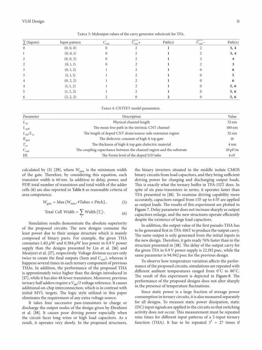
The proposed carry generator subcircuit for TFA isshown in Figure 4. Table 3 shows how transistors connectthe midoutputs 𝐶out+ and 𝐶out− to the proper voltage sourcedepending on what input pattern is considered (Table 3,Second Column), regardless of its permutations. Two-inputSum generator subcircuits (Figure 2(a)) are cascaded inseries to create the output Sum (Figure 3(c)). Although it isalso possible to obtain the final output Sum directly fromthe initial inputs, the number of pass-transistors in series
increases inside the body of the subcircuit, and hence it leadsto deficient overall performance. As a result, cascaded Sumgenerators are preferable. The entire full adder cell has 142transistors.
4. Simulation Results
High-performance and state-of-the-art CNTFET-baseddesigns are selected for comparison. Extensive simulationsetups are taken into account to examine new adder cellsin several aspects. All circuits are simulated with SynopsysHSPICE and 32 nm CNTFET technology [27, 28] inthree power supply voltages (1 V, 0.9 V, and 0.8V) atroom temperature. This compact SPICE model includes all

VLSI Design 9
THATFATFATFATFATFATFA
a6 a5 a4 a3 a2 a1 a0b6 b5 b4 b3 b2 b1 b0
c7 s6 s5 s4 s3 s2 s1 s0
Figure 11: A 7-TIT ternary ripple adder constructed by a THA and six TFAs.
A = 0 0 0 0 0 0 0B = 2 2 2 2 2 2 2 +
0 2 2 2 2 2 2 2
A = 0 0 0 0 0 0 1B = 2 2 2 2 2 2 2 +
1 0 0 0 0 0 0 0
+
1 1 0 0 0 0 0 1
A = 1 0 0 0 0 0 2B = 2 2 2 2 2 2 2
+
A = 0 0 0 0 0 0 1B =
1 0 0 0 0 0 0 0
2 2 2 2 2 2 2
+
A = 2 0 0 0 0 0 2B = 2 2 2 2 2 2 2
1 2 0 0 0 0 0 1
+
A = 1 0 0 0 0 0 1B = 2 2 2 2 2 2 2
1 1 0 0 0 0 0 0
A = 2 0 0 0 0 0 2B = 2 2 2 2 2 2 2 +
1 2 0 0 0 0 0 1
a0: 0→1
a0: 1→2
a0: 2→1
a0: 1→2
a0: 2→1
a0: 1→2
s6 : 2→0
s6 : 0→1
s6 : 1→0
s6 : 0→2
s6 : 2→1
s6 : 1→2
Figure 12: Input patterns which are fed to the ternary ripple adders to measure maximum delay.
nonidealities such as Schottky barrier effects, parasitic Drain/Source/Gate capacitances and resistances, and CNT chargeScreening Effects. A brief description of the parameters ofthe CNTFET model, which has been designed for unipolarMOSFET-like devices with one or more CNTs, is shown inTable 4.
Fan-out of 4 ternary inverters (FO4) was employed asthe output load in order to provide a realistic simulationsetup. Transient responses of the proposed THA and TFAin 100MHz operating frequency are plotted in Figures 5and 6, respectively. Average power consumption during all
transitions is also measured. Finally, power-delay product(PDP) is a balance between delay and power factors (4).Simulation results are shown in Table 5. The best results areshown in boldface for better clarification.
PDP = Max (Delay) × Avg (Power) . (4)
There are three nanotubes under the gate terminal of alltransistors (#Tubes = 3). Channel length is 32 nm (𝐿
𝑔=
32 nm), and the distance between the centers of two adjacentCNTs under the gate of a transistor is set 20 nm (Pitch =20 nm). Transistor width of a CNTFET can be approximately

10 VLSI Design
a
b
ba
ba
a
b
b a
GND
b a
a
GNDSum
a
b
a
b
48
b
a a
b b
GND
GND
100
48
180
100
250
60
4848
48300
300
450
150
250
60
180
100
100
48
180
180
180
180
180
180
6060
60
60
60
60
60
6060
60
600
600
300
300
48 48
250
250
250
250
180
180
60
60
600
600
180
180
180
180
48 48
0.289
0.289
0.289 0.289
0.289
0.289
0.289 0.289
0.2890.289
0.289
0.289
0.2890.289
0.289
0.289
0.289
0.289
0.289
0.289
0.289
0.289
0.289
0.289 0.289
0.289
0.289 0.289
0.289 0.289
0.2890.289
0.289
0.2890.289
0.2890.289
0.289
0.289
0.289
0.289
0.289
0.289
0.2890.289
0.289 0.549
0.549
0.549
0.549
0.549
0.549
0.549
0.549
0.549 0.549
0.549
0.549 Buffer
Buffer
Vdd
Vdd
Vdd
Vdd
a+
a+a+
a+
a+
a+
a−
a−
a−
a−
a−
b+
b+
b+
b+
b+
b+
b−
b−
b−
b−
b−
(a)
a
b
a
b
GND
GND
b a
a
b
0.289150
48
550
550 48
48
48
100
48
180
100
0.289250
0.289
0.289
0.2890.289
0.2890.2890.2890.289
0.289
0.289
0.289
60
0.5490.549
0.549
0.549
48
48
48
Buffer
48
Vdd Cout
Vth = 0.289VWgate = 450nm
a+ b+
(b)
Figure 13: MOSFET implementation of the proposed ternary half adder.
VLSI Design 11
Table 3: Midoutput values of the carry generator subcircuit for TFA.
∑ (Inputs) Input pattern 𝐶out 𝐶out+ Path(s) 𝐶out− Path(s)0 (0, 0, 0) 0 2 1 2 3, 41 (0, 0, 1) 0 2 1 2 3, 42 (0, 0, 2) 0 2 1 2 42 (0, 1, 1) 0 2 1 2 33 (0, 1, 2) 1 2 1 0 63 (1, 1, 1) 1 2 1 0 54 (0, 2, 2) 1 2 1 0 64 (1, 1, 2) 1 2 1 0 5, 65 (1, 2, 2) 1 2 1 0 5, 66 (2, 2, 2) 2 0 2 0 5, 6
Table 4: CNTFET model parameters.
Parameter Description Value𝐿 ch Physical channel length 32 nm𝐿𝑔eff The mean free path in the intrinsic CNT channel 100 nm𝐿dd/𝐿 ss The length of doped CNT drain/source-side extension region 32 nm𝐾gate The dielectric constant of high-k top gate 16𝑇ox The thickness of high-k top gate dielectric material 4 nm𝐶sub The coupling capacitance between the channel region and the substrate 20 pF/mEfi The Fermi level of the doped S/D tube 6 eV
calculated by (5) [29], where 𝑊min is the minimum widthof the gate. Therefore, by considering this equation, eachtransistor width is 60 nm. In addition to delay, power, andPDP, total number of transistors and total width of the addercells (6) are also reported in Table 6 as reasonable criteria ofarea competence.
𝑊gate ≈ Max (𝑊min, #Tubes × Pitch) , (5)
Total Cell Width = ∑𝑖
Width (𝑇𝑖) . (6)
Simulation results demonstrate the absolute superiorityof the proposed circuits. The new designs consume theleast power due to their unique structure which is mainlycomposed of binary parts. For example, the given THAconsumes 1.411 𝜇W and 0.384 𝜇W less power in 0.9V powersupply than the designs presented by Lin et al. [16] andMoaiyeri et al. [17], respectively. Voltage division occurs onlytwice to create the final outputs (Sum and 𝐶out), whereas ithappens several times in each ternary component of previousTHAs. In addition, the performance of the proposed THAis approximately twice higher than the design introduced in[17], while it has also 48 fewer transistors. Moreover, previousternary half adders require a𝑉dd/2 voltage reference. It causesadditional on-chip interconnection, which is in contrast withinitial MVL targets. The logic style utilized in this papereliminates the requirement of any extra voltage source.
It takes four successive pass-transistors to charge ordischarge the output nodes of the design given by Ebrahimiet al. [18]. It causes poor driving power especially whenthe circuit faces long wires or high load capacitors. As aresult, it operates very slowly. In the proposed structures,
the binary inverters situated in the middle isolate CMOSbinary circuits from load capacitors, and they bring sufficientdriving power for charging and discharging output loads.This is exactly what the ternary buffer in TFA-132T does. Inspite of six pass-transistors in series, it operates faster thanTFA presented in [18]. To examine driving capability moreaccurately, capacitors ranged from 1 fF up to 6 fF are appliedas output loads. The results of this experiment are plotted inFigure 7. Delay parameter does not increase sharply as outputcapacitors enlarge, and the new structures operate efficientlydespite the existence of large load capacitors.
In addition, the output value of the first pseudo-THA hasto be generated first in TFA-106T to produce the output carry.The same output is only generated from the initial inputs inthe new design.Therefore, it gets ready 76% faster than in thestructure presented in [18]. The delay of the output carry forthe given TFA in 0.9V power supply is 22.192 psec, while thesame parameter is 94.942 psec for the previous design.
To observe how temperature variation affects the perfor-mance of the proposed circuits, simulations are repeated withdifferent ambient temperatures ranged from 0∘C to 80∘C.The result of this experiment is depicted in Figure 8. Theperformance of the proposed designs does not alter sharplyin the presence of temperature fluctuations.
Since static power is a large fraction of average powerconsumption in ternary circuits, it is alsomeasured separatelyfor all designs. To measure static power dissipation, static(DC) input signals are applied to the circuits so that switchingactivity does not occur. This measurement must be repeatednine times for different input patterns of a 2-input ternaryfunction (THA). It has to be repeated 33 = 27 times if

12 VLSI Design
Table 5: Simulation results of one-digit adders.
Design𝑉dd = 0.8V 𝑉dd = 0.9V 𝑉dd = 1V
Delay(psec)
Power(𝜇W)
PDP(aJ)
Delay(psec)
Power(𝜇W)
PDP(aJ)
Delay(psec)
Power(𝜇W)
PDP(aJ)
Ternary half adderProposedTHA 38.74 0.282 10.94 28.42 0.880 25.01 25.43 2.778 70.66
THA byLin et al. [16] 91.40 0.771 70.43 66.64 2.291 152.7 54.03 5.817 314.3
THA byMoaiyeri et al. [17] 50.35 0.415 20.88 39.49 1.264 49.91 35.08 3.806 133.5
Ternary full adderProposedTFA 58.94 0.456 26.89 43.95 1.472 64.68 35.66 4.595 163.9
TFA byEbrahimi et al. [18] 189.5 0.597 113.1 139.4 1.893 263.9 116.8 5.463 638.3
TFA byKeshavarzian andSarikhani [19]
119.2 0.607 72.32 102.4 1.912 195.9 81.98 5.413 443.8
800m600m400m200m
0v(a)
v(b)
v(Sum)
v(cout)
200n
Volta
ges (
lin)
800m600m400m200m
0
Volta
ges (
lin)
400m
200m
0
0
Volta
ges (
lin)
500m
0
Volta
ges (
lin)
Time (lin)
Wave WaveD0: tr0: v(a)D0: tr0: v(b)
D0: tr0: v(Sum)D0: tr0: v(Cout)
Figure 14: Transient response of the proposed THA with MOSFETtechnology.
Table 6: Area comparison.
Design #Transistors Total cell width(nm)
Ternary half adderProposed THA 64 3840THA by Lin et al. [16] 158 9480THA by Moaiyeri et al. [17] 112 6720
Ternary full adderProposed TFA 142 8520TFA by Ebrahimi et al. [18] 106 6360TFA by Keshavarzian andSarikhani [19] 132 7920
a ternary function has three input variables (TFA). Theaverage and the maximum static powers are reported inTable 7. Static power dissipation reaches its minimum extentin the proposed designs due to their unique structure whichis mostly composed of binary parts. For instance, voltagedivision occurs only twice for the presented THA when allof the input variables equal “2,” whereas it happens six timesand four times in THA-158T and THA-112T, respectively.
Capability of working in high frequencies is put intopractice for the proposed structures as well. Figure 9 showshow sharply power increases by the increase of operatingfrequency from 100MHz to 1GHz. The new circuits operateefficiently in high frequencies, and they consume less powerthan previous designs.
One of the challenges in CNTFET fabrication is that thediameter of carbon nanotubes cannot be set very precisely.𝐷CNT varies with a standard deviation from 0.04 nm to0.2 nm for each mean diameter value [30]. To observe howtolerant the proposed designs are against process variation,Monte Carlo transient analysis is taken into consideration.

VLSI Design 13
Table 7: Static power comparison.
Design Average static power×10−7 (W)
Maximum static power×10−7 (W)
Ternary half adderProposed THA 5.2661 11.058THA by Lin et al. [16] 16.540 49.030THA by Moaiyeri et al. [17] 6.4400 18.767
Ternary full adderProposed TFA 6.4724 13.829TFA by Ebrahimi et al. [18] 10.897 21.250TFA by Keshavarzian and Sarikhani [19] 11.290 26.604
Table 8: Simulation results of 7-TIT ternary ripple adders.
Design Delay(psec)
Power(𝜇W)
PDP(fJ) #Transistors Total width
(nm)Ripple adder bythe proposed THA and TFA 187.84 7.5778 1.4234 916 54960
Ripple adder byTHA-112T and THF-132T 371.84 9.9079 3.6841 904 54240
This analysis is performed with a reasonable number of 30iterations, in which the simulation is repeated 10 times andthe largest deviation is reported. The statistical significanceof 30 iterations is quite high. There is a 99% probability thatover 80% of all possible component values operate properlyif a circuit operates correctly for all of the 30 iterations [31].Distribution of the diameter is assumed as Gaussian with6-sigma distribution, which is a reasonable assumption forlarge number of fabricated CNTs [32]. The results of thisexperiment are shown in Figure 10 for the proposed ternaryhalf adder, which is highly robust and tolerant against processvariation.
Single-bit adder cells are used to form larger adders.In order to test the practicability of the new designs in alarge circuit, a seven-Ternary digIT (7-TIT) ripple adder isconstructed by combining a THA and six TFAs (Figure 11).THA-112T and TFA-132T are also put together to formanother ternary ripple adder for comparison.
To measure worst-case delay, different input patterns arefed to the adder blocks (Figure 12) in a way that a transitionpropagates from the input of the first stage (𝑎
0) to the outputs
of the last stage (𝑠6). This input pattern is designed in a way
it causes all possible transitions in the output Sum of the laststage (𝑠
6). A long duration of iterative input pattern is also fed
to the adder blocks to measure average power consumption.Simulation results are reported in Table 8. Although theproposed ripple adder has a fewmore transistors, it consumesless power and it operates far faster than the structure built bythe previous adder cells.
Eventually, to provide a comparison between MOSFETand CNTFET technologies, the proposed ternary half adderis also implemented with 32 nm channel length bulk CMOS[33]. A brief description of the parameters of this modelis shown in Table 9. The MOSFET implementation of theproposed THA is illustrated in Figure 13. Each transistor is
marked with a pair of numbers. The upper number indicatesthreshold voltage and the lower number is the width of thetransistor (𝑊gate). Due to weaker on-current driving capabil-ity of bulk CMOS technology [34], buffers are supplemented,after the midoutputs are generated, to strengthen outputsignals. Driving power in MOSFETs is 3-4 times weakerthan CNTFETs [35]. Therefore, transistor widths are alsoextended enough to overcome this deficiency, paying theprice of enlarging area. Transient response of this adder cellis plotted in Figure 14. The whole cell is simulated underthe same conditions as mentioned before for the CNTFET-based THAs. Table 10 shows the simulation results of bothtechnologies. They demonstrate the fact that CNTFETs areabsolutely more promising candidates for ternary circuitry.The CNTFET-based THA operates 44 times faster, consumesapproximately 10 times less power, and occupies 3.3 times lessarea than its MOSFET counterpart.
5. Conclusions
New ternary adders have been proposed in this paper basedon a logic style which is mostly composed of binary parts.Therefore, static power consumption reaches its minimumamount. Extensive different analyses have been carried out toexamine efficiency in all aspects. The proposed designs ben-efit from low power consumption, high driving power, full-swing operation, and capability of working in low voltagesand high frequencies. They can be used in larger circuits andpractical environments.
A comparison between MOSFET and CNTFET hasbeen also provided to conclude the superior technologyfor ternary circuitry. Due to more flexibility of adjustingthe desired threshold voltage and high on-current drivingcapability, CNTFETs are definitely more promising devicesfor implementing ternary circuits in the future. Simulation

14 VLSI Design
Table 9: Bulk CMOS model parameters.
Parameter Description Value𝐿 ch Physical channel length 32 nm𝐿 eff The effective gate channel length 12.6 nm𝑅dsw The source and drain resistance per unit channel width 150Ω-𝜇m𝑇ox The gate oxide thickness 1 nm𝐶gbo The gate-to-bulk overlap capacitance per unit channel length 25.6 pF/m𝐶gdl/𝐶gsl The overlap capacitance between gate and lightly doped drain/source region 265.3 pF/m
Table 10: Simulation results of the new THA with MOSFET and CNTFET technologies.
Design Delay(psec)
Power(𝜇W)
PDP(fJ) #Transistors Total width
(nm)The proposed THA with MOSFET technology 1248 8.257 10.30 76 12762The proposed THA with CNTFET technology 28.42 0.880 0.025 64 3840
results confirm that a CNTFET-based ternary design sur-passes MOSFET implementation in terms of speed, powerconsumption, and area.
Conflict of Interests
The authors declare that there is no conflict of interestsregarding the publication of this paper.
References
[1] H. O. Ron, K. W. Mai, and A. Fellow, “The future of wires,”Proceedings of the IEEE, vol. 89, no. 4, pp. 490–504, 2001.
[2] E. Ozer, R. Sendag, and D. Gregg, “Multiple-valued logic busesfor reducing bus energy in low-power systems,” IEE Proceedings:Computers and Digital Techniques, vol. 153, no. 4, pp. 270–282,2006.
[3] E. Dubrova, “Multiple-valued logic in VLSI: challenges andopportunities,” in Proceedings of the NORCHIP ’99 Conference,pp. 340–349, 1999.
[4] B. Hayes, “Third base,” American Scientist, vol. 89, pp. 490–494,2001.
[5] S. L. Hurst, “Multiple-valued logic—its status and its future,”IEEE Transactions on Computers, vol. 33, no. 12, pp. 1160–1179,1984.
[6] Y.-B. Kim, “Integrated circuit design based on carbon nanotubefield effect transistor,” Transactions on Electrical and ElectronicMaterials, vol. 12, no. 5, pp. 175–188, 2011.
[7] Y. Yasuda, Y. Tokuda, S. Zaima, K. Pak, T. Nakamura, and A.Yoshida, “Realization of quaternary logic circuits by n-channelMOS devices,” IEEE Journal of Solid-State Circuits, vol. 21, no. 1,pp. 162–168, 1986.
[8] H. Inokawa, A. Fujiwara, and Y. Takahashi, “A multiple-valuedlogic with merged single-electron and MOS transistors,” inProceedings of the IEEE International Electron Devices Meeting(IEDM ’01), pp. 7.2.1–7.2.4, December 2001.
[9] S. Lin, Y.-B. Kim, and F. Lombardi, “A novel CNTFET-basedternary logic gate design,” in Proceedings of the 52nd IEEEInternational Midwest Symposium on Circuits and Systems(MWSCAS ’09), pp. 435–438, Cancun, Mexico, August 2009.
[10] J. Appenzeller, “Carbon nanotubes for high-performance elec-tronics: progress and prospect,” Proceedings of the IEEE, vol. 96,no. 2, pp. 201–211, 2008.
[11] A. Rahman, J. Guo, S. Datta, and M. S. Lundstrom, “Theoryof ballistic nanotransistors,” IEEE Transactions on ElectronDevices, vol. 50, no. 9, pp. 1853–1864, 2003.
[12] A. Bachtold, P. Hadley, T. Nakanishi, and C. Dekker, “Logiccircuits with carbon nanotube transistors,” Science, vol. 294, no.5545, pp. 1317–1320, 2001.
[13] V. Derycke, R. Martel, J. Appenzeller, and P. Avouris, “Carbonnanotube inter- and intramolecular logic gates,” Nano Letters,vol. 1, no. 9, pp. 453–456, 2001.
[14] M. M. Shulaker, G. Hills, N. Patil et al., “Carbon nanotubecomputer,” Nature, vol. 501, pp. 526–530, 2013.
[15] A. P. Dhande and V. T. Ingole, “Design & implementation of 2-bit ternary ALU slice,” in Proceedings of the International Con-ference on IEEE Science of Electronics, Technology of Informationand Telecommunication, pp. 17–21, 2005.
[16] S. Lin, Y.-B. Kim, and F. Lombardi, “CNTFET-based design ofternary logic gates and arithmetic circuits,” IEEE Transactionson Nanotechnology, vol. 10, no. 2, pp. 217–225, 2011.
[17] M. H. Moaiyeri, A. Doostaregan, and K. Navi, “Design ofenergy-efficient and robust ternary circuits for nanotechnol-ogy,” IETCircuits, Devices and Systems, vol. 5, no. 4, pp. 285–296,2011.
[18] S. A. Ebrahimi, P. Keshavarzian, S. Sorouri, and M. Shah-savari, “Low power CNTFET-based ternary full adder cell fornanoelectronics,” International Journal of Soft Computing andEngineering, vol. 2, pp. 291–295, 2012.
[19] P. Keshavarzian and R. Sarikhani, “A novel CNTFET-basedternary full adder,” Circuits, Systems, and Signal Processing, vol.33, no. 3, pp. 665–679, 2014.
[20] J. A. Mol, J. van der Heijden, J. Verduijn, M. Klein, F. Remacle,and S. Rogge, “Balanced ternary addition using a gated siliconnanowire,” Applied Physics Letters, vol. 99, no. 26, Article ID263109, 2011.
[21] A. Raychowdhury and K. Roy, “Carbon-nanotube-basedvoltage-mode multiple-valued logic design,” IEEE Transactionson Nanotechnology, vol. 4, no. 2, pp. 168–179, 2005.
[22] M. H. Moaiyeri, R. F. Mirzaee, A. Doostaregan, K. Navi, andO. Hashemipour, “A universal method for designing low-power

VLSI Design 15
carbon nanotube FET-basedmultiple-valued logic circuits,” IETComputers andDigital Techniques, vol. 7, no. 4, pp. 167–181, 2013.
[23] E. Trias, J. Navas, E. S. Ackley, S. Forrest, andM. Hermenegildo,Negative Ternary Set-Sharing, vol. 5366 of Lecture Notes inComputer Science, 2008.
[24] M.H.Moaiyeri, R. F.Mirzaee, K. Navi, andA.Momeni, “Designand analysis of a high-performance CNFET-based Full Adder,”International Journal of Electronics, vol. 99, no. 1, pp. 113–130,2012.
[25] Z. K. Tang, L. Y. Zhang, N. Wang et al., “One-dimensionalsuperconductivity in 0.4 nm single-walled carbon nanotubes,”Proceedings of the Electrochemical Society, pp. 587–595, 2002.
[26] M. S. Dresselhaus, G. Dresselhaus, and P. Avouris, CarbonNanotubes: Synthesis, Structure, Properties, and Applications,Springer, 2001.
[27] J. Deng, Device modeling and circuit performance evaluationfor nanoscale devices: silicon technology beyond 45nm node andcarbon nanotube field effect transistors [Ph.D. thesis], StanfordUniversity, 2007.
[28] “Stanford University CNFETModel,” http://nano.stanford.edu/models.phpwebsite.
[29] Y. B. Kim andY.-B. Kim, “High speed and low power transceiverdesign with CNFET and CNT bundle interconnect,” in Proceed-ing of the 23rd IEEE International SOC Conference (SOCC '10),pp. 152–157, Las Vegas, Nev, USA, September 2010.
[30] H. Shahidipour, A. Ahmadi, and K. Maharatna, “Effect ofvariability in SWCNT-based logic gates,” in Proceedings of the12th International Symposium on Integrated Circuits (ISIC ’09),pp. 252–255, December 2009.
[31] S. Lin, Y.-B. Kim, and F. Lombardi, “Design and analysis of a32 nm PVT tolerant CMOS SRAM cell for low leakage and highstability,” Integration, the VLSI Journal, vol. 43, no. 2, pp. 176–187,2010.
[32] K. El Shabrawy, K. Maharatna, D. Bagnall, and B. M. Al-Hashimi, “Modeling SWCNT bandgap and effective massvariation using a Monte Carlo approach,” IEEE Transactions onNanotechnology, vol. 9, no. 2, pp. 184–193, 2010.
[33] Predictive Technology Model, http://ptm.asu.edu.[34] C. Garcıa and A. Rubio, “Manufacturing variability analysis in
carbon nanotube technology: a comparison with bulk CMOSin 6T SRAM scenario,” in Proceedings of the 14th IEEE Inter-national Symposium on Design and Diagnostics of ElectronicCircuits and Systems (DDECS ’11), pp. 249–254, April 2011.
[35] F. Ali Usmani and M. Hasan, “Carbon nanotube field effecttransistors for high performance analog applications: an opti-mum design approach,” Microelectronics Journal, vol. 41, no. 7,pp. 395–402, 2010.

International Journal of
AerospaceEngineeringHindawi Publishing Corporationhttp://www.hindawi.com Volume 2014
RoboticsJournal of
Hindawi Publishing Corporationhttp://www.hindawi.com Volume 2014
Hindawi Publishing Corporationhttp://www.hindawi.com Volume 2014
Active and Passive Electronic Components
Control Scienceand Engineering
Journal of
Hindawi Publishing Corporationhttp://www.hindawi.com Volume 2014
International Journal of
RotatingMachinery
Hindawi Publishing Corporationhttp://www.hindawi.com Volume 2014
Hindawi Publishing Corporation http://www.hindawi.com
Journal ofEngineeringVolume 2014
Submit your manuscripts athttp://www.hindawi.com
VLSI Design
Hindawi Publishing Corporationhttp://www.hindawi.com Volume 2014
Hindawi Publishing Corporationhttp://www.hindawi.com Volume 2014
Shock and Vibration
Hindawi Publishing Corporationhttp://www.hindawi.com Volume 2014
Civil EngineeringAdvances in
Acoustics and VibrationAdvances in
Hindawi Publishing Corporationhttp://www.hindawi.com Volume 2014
Hindawi Publishing Corporationhttp://www.hindawi.com Volume 2014
Electrical and Computer Engineering
Journal of
Advances inOptoElectronics
Hindawi Publishing Corporation http://www.hindawi.com
Volume 2014
The Scientific World JournalHindawi Publishing Corporation http://www.hindawi.com Volume 2014
SensorsJournal of
Hindawi Publishing Corporationhttp://www.hindawi.com Volume 2014
Modelling & Simulation in EngineeringHindawi Publishing Corporation http://www.hindawi.com Volume 2014
Hindawi Publishing Corporationhttp://www.hindawi.com Volume 2014
Chemical EngineeringInternational Journal of Antennas and
Propagation
International Journal of
Hindawi Publishing Corporationhttp://www.hindawi.com Volume 2014
Hindawi Publishing Corporationhttp://www.hindawi.com Volume 2014
Navigation and Observation
International Journal of
Hindawi Publishing Corporationhttp://www.hindawi.com Volume 2014
DistributedSensor Networks
International Journal of


