Embed Size (px)
Citation preview

Hole states in Ge/Si quantum-dot molecules produced by strain-drivenself-assembly
A. I. Yakimov,a� G. Yu. Mikhalyov, A. V. Dvurechenskii, and A. I. NikiforovRzhanov Institute of Semiconductor Physics, Siberian Branch of the Russian Academy of Sciences,630090 Novosibirsk, Russia
�Received 27 July 2007; accepted 17 September 2007; published online 13 November 2007�
Space-charge spectroscopy was employed to study hole emission from the confined states invertically self-aligned double Ge quantum dots separated by a Si barrier. From the temperature- andfrequency-dependent measurements, the hole binding energy was determined as a function of theseparation between the dots, tSi. Increasing of the ground state hole energy due to formation of abonding molecular orbital was found to be as large as �50 meV at tSi=1.5 nm. For a dot layerseparation exceeding 3 nm, the hole binding energy in double-dot molecule becomes smaller thanthe ionization energy of the single Ge dot, contrasting with a simplified quantum-mechanicalmolecular model. To analyze the experiment the electronic structure of two vertically coupledpyramidal Ge quantum dots embedded in Si was investigated by a nearest neighbor tight-bindingsingle-particle Hamiltonian with the sp3 basis. The elastic strain due to the lattice mismatch betweenGe and Si was included into the problem. The three-dimensional spatial strain distribution wasfound in terms of atomic positions using a valence-force-field theory with a Keating interatomicpotential. It was demonstrated that formation of single-particle hole states in self-organizedmolecules is governed by the interplay among two effects. The first is the quantum-mechanicalcoupling between the individual states of two dots constituting the molecule. The second oneoriginates from asymmetry of the strain field distribution within the top and bottom dots due to thelack of inversion symmetry with respect to the medium plane between the dots. Analysis of thebiaxial strain distribution showed that anomalous decreasing of the hole binding energy below thevalue of the single dot with increasing interdot separation is caused by the partial strain relaxationupon dot stacking accompanied by the strain-induced reduction of the hole confinement potential.We found that the molecule-type hole state delocalized fairly over the two dots is formed only attSi�3.3 nm and at tSi�3.8 nm. For the intermediate distances �3.3 nm� tSi�3.8 nm�, the holebecomes confined mostly inside the bottom, most strained Ge dot. The overall agreement betweentheory and experiment turns out to be quite good, indicating the crucial role played by strain fieldsin electronic coupling of self-assembled quantum-dot molecules. © 2007 American Institute ofPhysics. �DOI: 10.1063/1.2809401�
I. INTRODUCTION
Coherent two-level systems and the quantum logic gatesare suggested to serve as the building blocks of a quantuminformation processing.1–4 Two vertically5,6 or laterally7–9
coupled quantum dots �QDs� confined electrons, holes, orexcitons have been proposed as a basis for entangled quan-tum bit operations in the solid state. Spin or charge degreesof freedom are exploited for encoding and manipulatingquantum information. Apart from the obvious practical uses,“artificial molecules” are extremely interesting also from thefundamental point of view, since the relative contribution ofsingle-particle tunneling and Coulomb interaction in themcan be varied in a controllable way.10 The electronic cou-pling between QDs brought closely together arises from theprocess of quantum-mechanical tunneling and appears as aformation of bonding and antibonding molecule-type orbitalsfrom the single-dot states �Fig. 1� by an analogy with thecovalent bonds in natural molecules. The bonding molecularstate has a larger binding energy than the energies of the
original states of the individual dots, thus creating the bind-ing force between the two dots. The collectivized electronbehaves now as a coherent wave that is delocalized over bothconstituent QDs.
A number of transport experiments have been made withartificial molecules composed of QDs in which the lateralconfinement was achieved either via etching techniques ormetal gate electrodes.7,8,11–14 However, the size of thesestructures is too large ��50–100 nm� and the interlevelspacing is too small ��1 meV� to operate a device at el-evated temperatures. The phenomenon of strain-induced self-assembly of semiconductor nanostructures provides anothermethod that allowed for the fabrication of high-quality ver-tically aligned QDs whose size is extremely small��10 nm� and the electronic state resembles certainly thoseof an atom even at room temperature. During heteroepitaxialgrowth of lattice mismatched materials strain field of a dot ina first layer penetrates into the barrier material and makes itfavorable for the dot on the upper layer to form above theburied QD,15 thus forming a vertical QD molecule �QDM�.Inhomogeneous spatial strain distribution is a characteristica�Electronic mail: [email protected]
JOURNAL OF APPLIED PHYSICS 102, 093714 �2007�
0021-8979/2007/102�9�/093714/11/$23.00 © 2007 American Institute of Physics102, 093714-1
Downloaded 14 Nov 2007 to 194.226.178.12. Redistribution subject to AIP license or copyright, see http://jap.aip.org/jap/copyright.jsp

feature of self-assembled QDMs that distinguish them fromelectrostatically confined nanostructures. The hydrostaticcomponent of strain usually shifts the conduction and va-lence band edges of semiconductor; biaxial strain, on theother hand, affects the valence bands by splitting the degen-eracy of the light- and heavy-hole bands. Since the strainmodifies the confinement potential and the carrier effectivemasses, it may cause considerable deviations from the sim-plified molecular behavior which implies a coupling of iden-tical QDs.
To date, most theoretical16–20 and experimental6,21–27
studies on the molecular states in stacked QDs have beenconcentrated on self-assembled InAs/GaAs QDs. Luyken etal.21 concluded that the many-body ground states of verti-cally aligned InAs QDs are mainly affected by interdot Cou-lomb coupling. Boucaud et al.22 observed the terahertz�2.4 THz� absorption caused by transition between bondingand antibonding electron states in InAs/GaAs. Fonseca etal.16 found that anisotropy in the strain field and associatedpiezoelectric potential leads to enhancing level splitting forelectron molecular states. Sheng and Leburton19 reported theanomalous quantum-confined Stark effect caused by the bi-axial strain distribution in InAs/GaAs QD molecules. Theresonant current with peak-to-valley ratio above 1000 wasdetected by Bryllert et al.25 for a single InAs/ InP QDM. Heet al.20 demonstrated that a molecule made of two identical,strained InAs/GaAs QDs exhibits asymmetry of the molecu-lar orbitals due to inhomogeneous strain.
The Coulomb charging effect was also observed indouble-layer GeSi QDs occupied with holes.28,29 Ge quan-tum dots in Si�001� �4.2% lattice mismatch� is another sys-tem exhibiting a self-organization of nanostructures in semi-conductor heteroepitaxy.30 The large ��0.7 eV� valenceband offset of Ge/Si�001� heterojunction leads to effectivelocalization of holes in the Ge islands, whereas the electronsare free in the Si conduction band.31 Usually, the behavior ofholes in low-dimensional systems is more complicated thanthat of electrons because of the complex valence band struc-ture in III-V and IV semiconductors. The hole state in GeQD is built mainly from valence-band states, namely, heavy-
hole states � 32 , ± 3
2 �, the light-hole states � 32 , ± 1
2 �, and the split-off hole states � 1
2 , ± 12 �. Here, �J ,Jz� are the eigenstates of the
effective angular momentum J and its projection Jz. Thestrong mixing between the light- and heavy-hole states is aresult of the uncertainty in all components of quasi-impulseowing to hole spatial confinement both in vertical and lateraldirections.32 In uniaxially strained semiconductors, strainslifts the degeneracy of the valence band, making the heavyhole states to be the highest valence band.33 For this reason,the contribution of the heavy hole states in the ground stateof QDs must be predominant. As demonstrated by tight-binding calculations,34 in Ge nanoclusters with lateral size of�15 nm and height of �1.5 nm, the contribution of the statewith Jz= ± 3
2 is about 90%. Because the strain extends intothe barrier material, the strain field within one QD is affectedby a neighboring dot as well. One can expect that redistribu-tion of strain fields during vertical stacking of Ge dots wouldsubstantially modify the band structure which, in turn, willstrongly affect the formation of molecular orbitals.
In this paper we analyzed both experimentally and theo-retically the single-particle hole ground state of doubleGe/Si quantum dot representing an ionized “artificial hydro-gen molecule” containing a hole instead of an electron. Weobserved that the ground-state configuration undergoes non-trivial transformations as a function of the interdot distancedue to the competition of the tunneling and deformation ef-fects.
II. EXPERIMENTAL DETAILS
Samples were grown by molecular-beam epitaxy on ap+−Si�001� substrate with a resistivity of 0.005 � cm dopedwith boron up to a concentration of �1019 cm−3. After pre-liminary chemical processing, the substrates were placed inthe growth chamber where they were cleaned by a weak Siflux at 800 °C for 15 min. As a result of cleaning, an atomi-cally pure surface with a sharp �2�1� diffraction pattern isformed. The growth temperature was 500 °C for all layers.The active region consists of two nominally pure Ge layersseparated by Si spacer layer of thickness tSi �Fig. 2�a��. Im-mediately after the deposition of Ge, the temperature waslowered to Ts=350–400 °C and the Ge islands are coveredby a 1 nm Si layer. This procedure is necessary to minimizeGe–Si intermixing and to preserve island shape and sizefrom the effect of a further higher temperaturedeposition.35–38 In order to reduce distortion of the hole con-fining potential by the potential of ionized impurities, 10 nmthick undoped Si spacers were introduced between the top-most �bottom� Ge layer and the p-type Si cover �buffer�layer. The boron concentration in the 0.35 �m thick cap and0.5 �m thick buffer Si layers was �4�1016 cm−3. To iden-tify effects of dot coupling, the reference sample was grownunder conditions similar to the QDM samples, except thatonly a single Ge layer was deposited.
The Ge QD formation was controlled by reflection highenergy electron diffraction when the pattern changed fromstreaky to spotty. The transition from two-dimensional tothree-dimensional island growth was observed after �4monolayers � 1 ML=1.41 � of Ge deposition both for the
FIG. 1. Schematic picture of energies of the two low-lying electron states ina QD molecule as a function of the separation between the dots. The bond-ing orbital �+ � is a symmetric linear superposition of the single-dot states �0�and �1�: �+ �= ��0�+ �1�� /�2, while the antibonding state represents the anti-symmetric wave function combination: �−�= ��0�− �1�� /�2.
093714-2 Yakimov et al. J. Appl. Phys. 102, 093714 �2007�
Downloaded 14 Nov 2007 to 194.226.178.12. Redistribution subject to AIP license or copyright, see http://jap.aip.org/jap/copyright.jsp

first and second Ge layers. The Ge growth rate was chosen tobe as large as R=1 ML/s to provide the high Ge content inthe islands.39 The average Ge content of 80%–90% �depend-ing on tSi� in the nanoclusters was determined from Ramanmeasurements. The scanning tunneling microscopy �STM� ofsamples without the Si cap layer was employed to assess themorphology of Ge layers. Figures 3�a� and 3�b� show theSTM images of the topmost Ge layer for single and double-layer samples, and the lateral size histogram derived derivedfor each image. In good qualitative agreement with the re-sults obtained previously in Refs. 40 and 41, the surfacemorphology is approximately the same for the single anddouble island layers, and changes significantly with furtherincreasing of the number of Ge layers in the structure. Al-though, some of the islands did not have a square base, weused their geometrical mean, l=�l � l� �l and l� are theisland base lengths�, as a convenient measure of their size.From these data, the width of the size distribution, �, wascalculated as standard deviation,
�2 =1
n − 1i=1
n
�li − �l��2,
where n is the number of islands evaluated, and �l� is themean size. Ge nanoclusters have a shape of “hut” clustersbounded by �105 facets42 with predominantly square basesin two orthogonal orientations, corresponding to �100� direc-tions in the substrates. The dots have a typical base length�l��10–11 nm and an areal density nQD=1.5�1011 cm−2.The nonuniformity of island size is estimated to be about
16%–18%. Figure 3�e� shows a representative cross-sectional transmission electron micrograph �TEM� of adouble-layer sample with tSi=3.5 nm. The image clearlydemonstrates the formation of double-dot molecules with ahigh vertical correlation between Ge islands.
For the capacitance and conductance measurements, Alcontacts were deposited on top of the samples through ashadow mask to form a Schottky diode, while the Ohmicback contact was fabricated by alloying indium to thep+-type Si substrate. The area of the Al contacts was A=8�10−3 cm2. Just before the metallization, a 30 nm top Silayer was etched off to remove any remaining contaminationfrom the surface. The admittance was measured using aFluke PM6306 RLC meter in the frequency range from100 Hz to 1 MHz. The amplitude of the ac modulation volt-age was 50 mV. At each frequency, the RLC meter was care-fully calibrated to compensate for the parasitic resistancefrom the measurement circuit. A Keithley 6430 subfemtoam-pere remote source meter was used for supplying a dc biasvoltage. Both meters were controlled by the computer systemthrough the IEEE-488 interfaces.
III. DATA ANALYSIS PROCEDURE
A. Determination of the hole binding energies
To determine the hole binding energy we measured thehole thermal emission rates at different temperatures usingadmittance spectroscopy. In these experiments, the ac con-ductance G of a pn junction or Schottky diode with the elec-
FIG. 2. �a� A schematic valence band diagram of the Si Schottky diodecontaining a double stack of Ge QDs and a sketch of the sample structure.The p+-Si substrate is not shown. �b� Equivalent electrical circuit for the acresponse from the dots lying inside the depletion region. Ccap is the capaci-tance of the totally depleted capping Si layer, Cbuff the capacitance of thedepleted portion of the buffer Si layer, CQD the QD capacitance, and RQD thehole emission and capture resistance.
FIG. 3. 400�400 nm2 STM images ��a� and �b�� and size distribution his-tograms ��c� and �d�� from topmost uncapped Ge layer of single ��a� and �c��and double ��b� and �d�� island layers deposited at a substrate temperature of500 °C with the rate of R=1 ML/s. For the twofold stack in panels �b� and�d�, the separation between Ge layers is 3 nm. Image sides are orientedalong the �110� crystalline directions. �e� Cross-section TEM image in �001�direction of coupled Ge QDs separated by a Si barrier with 3.5 nm thick-ness. Arrows indicate vertically coupled double quantum dots.
093714-3 Yakimov et al. J. Appl. Phys. 102, 093714 �2007�
Downloaded 14 Nov 2007 to 194.226.178.12. Redistribution subject to AIP license or copyright, see http://jap.aip.org/jap/copyright.jsp

tronic states of interest is measured as a function of tempera-ture for a fixed reverse bias Ub and test frequency �=2f .For a given measurement frequency, the conductance reachesa maximum at a temperature Tmax which corresponds to thecondition43
� � 2ep�Tmax� , �1�
where
ep�T� = B�pT2 exp�− Ea/kBT� �2�
is the emission rate of electrons or holes from the bound toextended states, B=16m*kB
2 /gth3 is a temperature indepen-
dent factor, m* is the effective mass of the density of states,gt is the degeneracy of a quantum level, h is the Plank’sconstant, �p is the capture cross section, kB is the Boltzmannconstant, and Ea is the activation energy being determined bythe actual path whereby holes escape from the dots to the Sivalence band. By measuring the G�T� dependencies at vari-ous �, the activation energies of hole emission rate and thecapture cross section �p can be deduced from the Arrheniusplot of ep�Tmax� /Tmax
2 vs 1/Tmax. With changing of the re-verse bias Ub, the chemical potential scans through the den-sity of hole states in the QD layer �Fig. 2�a��. At higherreverse bias, the chemical potential crosses deeper states inthe dots. Thus, from the bias-variable temperature- andfrequency-dependent measurements the energy of hole emis-sion from different confined states can be determined.
B. Effect of electric field on the hole thermal emission
In a simple scenario of emission by thermal excitationfrom the localized states in the QD layer to the continuum,Ea corresponds to the binding energy of holes with energiesclose to the Fermi level. In more complex cases Ea maydeviate from this energy. The electron escape process inInAs/GaAs QDs is known to be a two-step process43–48
which involves thermal activation to the excited state wherethe tunnel probability is more favorable and then subsequenttunneling into the GaAs conduction or valence band by theassistance of electric field. Therefore, both the localizationenergy and the electric field are important for the electronemission from QDs with a small carrier effective mass. InGe/Si QDs, hole tunneling should be vastly suppressed fordue to the large hole effective mass in Si �mh
*=0.49m0� andthe large localization energy �300–400 meV�,49–54 thus mak-ing the hole emission to be purely thermally activated. Asdescribed by Chang et al.44 and Geller et al.,48 the apparentcapture cross section �p is expected to grow in electric fielddue to increasing transparency of a triangle tunneling barrier.Instead, we observed the opposite behavior �see, Fig. 9� thatsignals against the importance of field-assisted tunneling pro-cess in our samples.
To obtain further support for this statement, we esti-mated the possible effect of electric field on the hole emis-sion rate. The estimation is based on the model of Vincent etal.55 who considered phonon-assisted tunneling between aDirac well and an energy band. The ratio of the thermalemission rate with or without electric field is representedby55
ep�F�
ep�0�= 1 + �
0
Ea�0�/kBT
exp�z − z3/2�4
3
�2mh*�1/2kBT3/2
qF��dz ,
�3�
where Ea�0� is the hole binding energy in zero field, and F isthe electric field strength. The field-assisted tunneling be-comes important when
T � Tc =�qF�2/3
kB�8mh*�1/3 . �4�
We calculated the mean electric field across the dots on thebasis of the quasistatic charging model and self-consistentcalculations of Poisson equation described in Ref. 54. At theonset of dot charging with holes, F�3�106 V/m. In thisway, we find Tc=60 K, while all measurements in this workwere performed at T�150 K.
The phenomenon of field-assisted tunneling via the wet-ting layer in Ge dots may take place when the number ofconfined holes in each Ge island is large enough ��10� pro-ducing a strong electric field around the islands,56 which isnot the case for the samples under investigation. Thus, effectof the two-step escape on the hole emission energy in Ge/SiQDs may not be taken into account in the present study.
A further possible manifestation of the electric field is alowering of the emission barrier by the field F due to thePoole-Frenkel effect.45,47,57 Assuming a square-well confine-ment in field direction the true emission energy differs fromthe measured activation energy by U=qFh /2, where h isthe QD height. We find that, for the bias applied here, U isless than 3 mV implying that the barrier lowering effect alsoplay a minor role in our samples.
C. Determination of the average dot filling factor
For a given QDM density nQD one may introduce theaverage number of extra holes per each molecule �, which byanalogy with quantum Hall effect can be called the fillingfactor. The average molecule filling factor is controlled bythe gate voltage Ub and defined by
��Ub� = pQD�Ub�/nQD, �5�
where pQD�Ub� is the hole density in the dot layer �here, weassume that the dot density in the single-layer sample isequal to the density of “diatomic” molecules in the double-layer samples�. Usually the charge density is derived usingC-V profiling procedure. However, for the case of a hetero-junction, the measured apparent carrier concentration differsfrom the true local carrier concentration due to Debye lengthsmearing.58 Therefore, we used another approach. The equi-librium density of holes accumulated in QDs was extractedfrom the capacitance of the dot or molecule layer using theequation
pQD�Ub� =1
qA�
u0
u
CQD�u�du , �6�
where CQD is the quantum-dot-layer capacitance, u is the theelectrostatic potential at the position of the dot layer causedby dot charging at the applied bias Ub, u0 corresponds to a
093714-4 Yakimov et al. J. Appl. Phys. 102, 093714 �2007�
Downloaded 14 Nov 2007 to 194.226.178.12. Redistribution subject to AIP license or copyright, see http://jap.aip.org/jap/copyright.jsp
bias at which all holes escape from QDs and CQD�u0�=0.The value of u0 can be determined from known doping levelby a procedure described in Ref. 59.
In order to evaluate the QD capacitance it is necessary toconstruct the equivalent electrical circuit which reproducesthe ac response from the dots. For simplicity we consideronly biases for which the depletion width of the metal-semiconductor �Al–Si� junction extends to the QD layer. Inour samples, capacitance-voltage measurements �Sec. IV A�demonstrate that QDs lie inside the depletion region just atUb�0–1 V depending on the sample. From Anand et al.,57
an ac response from the dots can be treated as a lossy capaci-tor of time constant �=RQDCQD. In this case the equivalentcircuit consists of the depletion capacitance of the Si caplayer Ccap in series with a parallel combination of the capaci-tance of the depleted part of the Si buffer layer Cbuff andseries RC network with the quantum-dot capacitance CQD
and time constant � �Fig. 2�b��. The cap layer capacitanceCcap is easily calculated with known values of device area Aand the cap layer thickness L. Ccap is assumed to be indepen-dent of Ub, �, and T and equals to Ccap=��0A /L, where �and �0 are the relative and absolute permittivities, respec-tively.
Now the relationship between u and gate voltage Ub canbe determined from60
u�Ub� − u0 = − �Ub0
Ub �1 −C0�Ub��
Ccap�dUb�, �7�
where Ub0 is the reverse bias at which QDs are neutral, C0 isthe sample capacitance in the low-frequency limit ����1�.The capacitance contribution given by the holes in QDs isdeduced from the frequency-dependent C-V measurements,
CQD�Ub� = � 1
C0�Ub�−
1
Ccap�−1
− � 1
C��Ub�−
1
Ccap�−1
,
�8�
where C��Ub� is the high-frequency device capacitance.Analysis of the experimental C-V characteristics by usingEqs. �5�–�8� allows one to calibrate the relationship betweenthe average dot filling factor and the gate voltage.61
D. Hole states treated with tight-binding approach
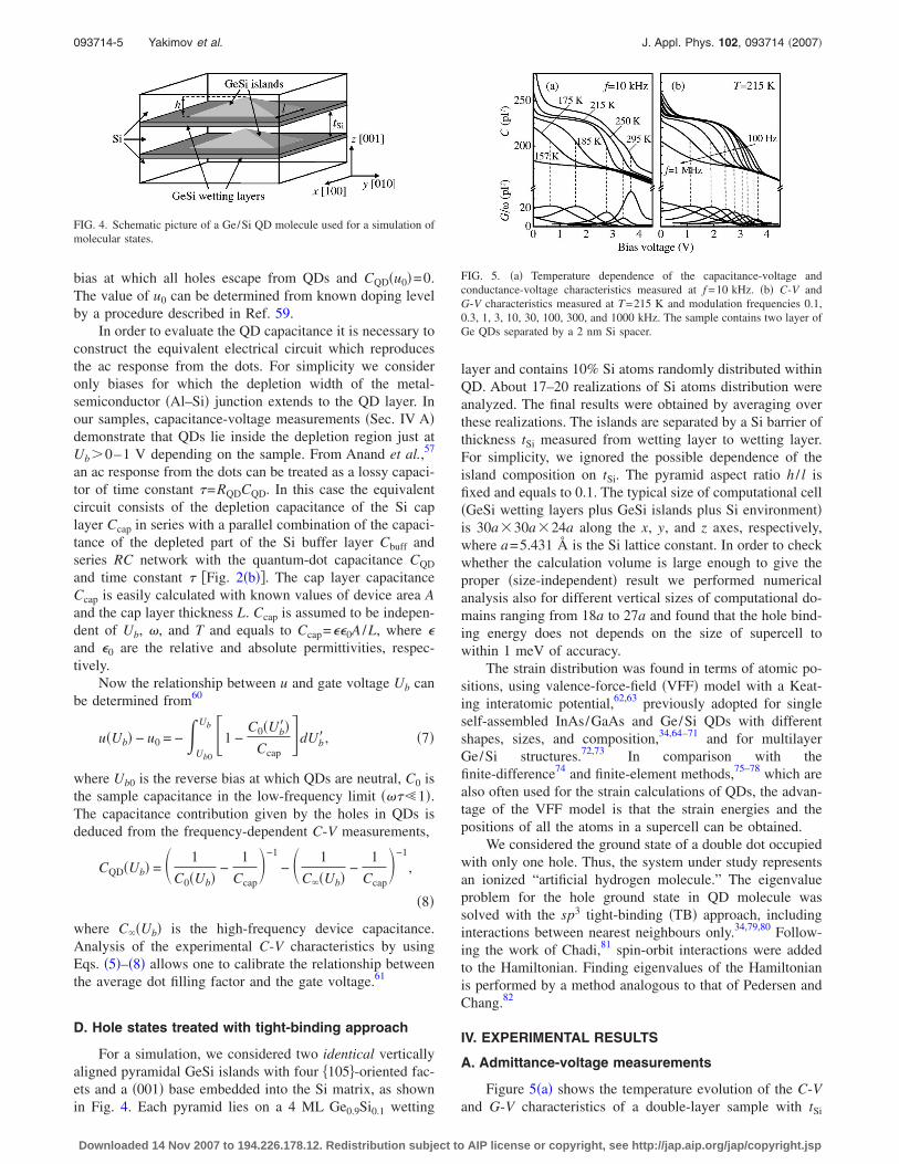
For a simulation, we considered two identical verticallyaligned pyramidal GeSi islands with four �105 -oriented fac-ets and a �001� base embedded into the Si matrix, as shownin Fig. 4. Each pyramid lies on a 4 ML Ge0.9Si0.1 wetting
layer and contains 10% Si atoms randomly distributed withinQD. About 17–20 realizations of Si atoms distribution wereanalyzed. The final results were obtained by averaging overthese realizations. The islands are separated by a Si barrier ofthickness tSi measured from wetting layer to wetting layer.For simplicity, we ignored the possible dependence of theisland composition on tSi. The pyramid aspect ratio h / l isfixed and equals to 0.1. The typical size of computational cell�GeSi wetting layers plus GeSi islands plus Si environment�is 30a�30a�24a along the x, y, and z axes, respectively,where a=5.431 Å is the Si lattice constant. In order to checkwhether the calculation volume is large enough to give theproper �size-independent� result we performed numericalanalysis also for different vertical sizes of computational do-mains ranging from 18a to 27a and found that the hole bind-ing energy does not depends on the size of supercell towithin 1 meV of accuracy.
The strain distribution was found in terms of atomic po-sitions, using valence-force-field �VFF� model with a Keat-ing interatomic potential,62,63 previously adopted for singleself-assembled InAs/GaAs and Ge/Si QDs with differentshapes, sizes, and composition,34,64–71 and for multilayerGe/Si structures.72,73 In comparison with thefinite-difference74 and finite-element methods,75–78 which arealso often used for the strain calculations of QDs, the advan-tage of the VFF model is that the strain energies and thepositions of all the atoms in a supercell can be obtained.
We considered the ground state of a double dot occupiedwith only one hole. Thus, the system under study representsan ionized “artificial hydrogen molecule.” The eigenvalueproblem for the hole ground state in QD molecule wassolved with the sp3 tight-binding �TB� approach, includinginteractions between nearest neighbours only.34,79,80 Follow-ing the work of Chadi,81 spin-orbit interactions were addedto the Hamiltonian. Finding eigenvalues of the Hamiltonianis performed by a method analogous to that of Pedersen andChang.82
IV. EXPERIMENTAL RESULTS
A. Admittance-voltage measurements
Figure 5�a� shows the temperature evolution of the C-Vand G-V characteristics of a double-layer sample with tSi
FIG. 4. Schematic picture of a Ge/Si QD molecule used for a simulation ofmolecular states.
FIG. 5. �a� Temperature dependence of the capacitance-voltage andconductance-voltage characteristics measured at f =10 kHz. �b� C-V andG-V characteristics measured at T=215 K and modulation frequencies 0.1,0.3, 1, 3, 10, 30, 100, 300, and 1000 kHz. The sample contains two layer ofGe QDs separated by a 2 nm Si spacer.
093714-5 Yakimov et al. J. Appl. Phys. 102, 093714 �2007�
Downloaded 14 Nov 2007 to 194.226.178.12. Redistribution subject to AIP license or copyright, see http://jap.aip.org/jap/copyright.jsp

=2 nm for a test frequency of f =10 kHz. Similar graphswere also obtained for the other samples. At Ub�0.5 V, themeasured capacitance is smaller than the depletion capaci-tance of the Si cap layer Ccap=250 pF. This means that thetotal depletion width exceeds the cap Si layer thickness Lcap
and the depletion region of the metal-semiconductor junctiondoes really extends beyond the QD layer. Thus, the equiva-lent circuit model displayed in Fig. 2�b� is relevant for thedata analysis procedure. At high temperature, there is a well-pronounced capacitance plateau from 0.5 to 3.6 V associatedwith the positive charge accumulation in the dot layers.83 Thewidth of a plateau depends on the steady-state occupation ofhole levels in the dots. Due to the p-type doping in the Simatrix, the Ge QDs are charged by holes at a zero bias.When a reverse bias is applied to the diode, the holes aregradually swept from the shallower QD states to the deeperstates. At Ub�3.6 V, all holes escape from the QDs and theQD contribution to the measured capacitance disappears. Thecorresponding step in the capacitance is accompanied by thepeak in the measured parallel conductance at voltage Up nearthe edge of the capacitance plateau. The emergence of a con-ductance peak can be regarded as a fingerprint of a resonantcondition for charging/discharging the QDs, which is ��=1.The characteristic time � for hole exchange between the dotsand the barrier depends on both the QD confined energiesand the temperature. At low temperatures, holes freeze ontodeep states in the dots and do not participate in the ac re-sponse. Therefore, as the temperature is reduced, the capaci-tance plateau is suppressed and the conductance peak shiftstowards lower biases, at which the applied ac frequency reso-nates with emission rate from shallower QD states.
Similarly, the resonant condition should be fulfilled at alower bias for a higher frequency. Figure 5�b� shows the C-Vand G-V characteristics recorded at T=215 K for differenttest frequencies. A clear shift of the capacitance step and theconductance maximum towards lower biases is seen as thefrequency is increased. This is consistent with the argumentsoutlined above. We considered capacitance-voltage tracestaken at f =100 Hz and 1 MHz as the steady-state �low-frequency� and the high-frequency characteristics, respec-tively, for the calculation of the QDM filling factor � �Sec.III C�. Bias dependence of the density of holes accumulatedon deep levels of dots and possible defects, determined asdescribed in Sec. III C, is shown in Fig. 6.
B. Temperature dependence of admittance
The typical temperature dependencies for the normalizedconductance measured at different modulation frequenciesand bias voltages are displayed in Fig. 7. The behavior ofG�T� /� can be qualitatively explained as follows. At a fixedbias, the charging/discharging process corresponds to the QDhole level coinciding with the Fermi level in undepleted partof the p-Si buffer layer. The rate of hole emission from thislevel becomes more slow when the temperature is reduced;therefore, with a decrease in the modulation frequency, thecondition for the conductance maximum �1� is satisfied atlower temperatures �Fig. 7�a��. With an increase in reversebias, the holes localized at deeper QD levels, for which con-
dition �1� at a fixed frequency is satisfied at higher tempera-tures, contribute to the admittance signal. For this reason, theconductance peak in Fig. 7�b� shifts towards higher tempera-tures with increasing Ub. At Ub�3.4 V, Ge QDs becomecompletely depleted and the maximum on the G�T� /� curvesdisappears. This is consistent with the observation from theC-V measurements of the same sample.
Figure 8 shows the representative dependenciesep /Tmax
2 �Tmax−1 � obtained using Eq. �1� from the temperature
variation of conductance under different modulation frequen-cies. The activation energy Ea of the hole emission rate wasfound from the slope of the approximating straight lines, andthe capture cross section was determined from the point ofintersection of the approximating lines and the ordinate axis.The linear correlation coefficients of all the lines are largerthan 0.9997 ensuring the good accuracy of the data deducedfrom the plots. The capture cross section �p has the value ofabout 10−13 cm2 �Fig. 9�, typical for self-assembledQDs,46,48,84,85 and decreases at large reverse bias due partici-pating of deep defect traps in the capture process �see be-low�.
The resulting activation energies of the hole emissionrate of a series of samples with twofold stacks of Ge islands
FIG. 6. Density of holes accumulated on deep localized states as a functionof the reverse bias. The data were obtained from the low- and high-frequency capacitance-voltage characteristics as described in Sec. III C.
FIG. 7. �a� Temperature dependence of the normalized conductance G /�recorded at Ub=0.8 V and modulation frequencies 1, 2, 3, 5, 10, 20, 30, 50,100, 200, 300, 500, 700, and 1000 kHz. �b� Temperature dependence of theconductance measured at modulation frequency f =10 kHz under differentbias voltages. The reverse bias is increased from Ub=0–3.6 V with an in-crement of 0.2 V. Each conductance curve has been offset by 3 pF in panel�a� and by 2.5 pF in panel �b� for clarity. The sample contains two layer ofGe QDs separated by a 2 nm Si spacer.
093714-6 Yakimov et al. J. Appl. Phys. 102, 093714 �2007�
Downloaded 14 Nov 2007 to 194.226.178.12. Redistribution subject to AIP license or copyright, see http://jap.aip.org/jap/copyright.jsp

are presented in Fig. 10 as a function of Ub /Up ratio, whereUp is the bias voltage at which the conductance peak appearsin the low-frequency conductance-voltage characteristics. Inour experimental conditions, Up varies from 2.1 to 5.5 V fordifferent samples. Near the edge of capacitance plateau �i.e.,at Ub /Up�1�, the activation energy turns out to be the samefor all samples. Its value, �0.38 eV, is much larger than theground state hole energy in the dots �see Sec. V�. The corre-sponding hole traps are visible as an additional concentrationpeak at a depth of �0.4 �m in the bulk carrier concentrationprofiles deduced from the low-frequency capacitance-voltagecharacteristics �Fig. 11�. The 0.38 eV level in boron-dopedSi is plausibly attributed to oxygen-carbon defectcomplexes,86 and is often observed as a sharp photolumines-cence line at about 0.76 eV in many experiments on SiGeheterostructures.87 An exact identification of the origin ofthis trap would need further investigation and is beyond thescope of this study. By integrating the defect-related peak ofthe concentration profiles over the depth we found the defectdensity to be �8±1��1010 cm−2 in the samples under inves-tigation. This number was subtracted from the total equilib-rium density of trapped holes when we determined the QDMfilling factor from the C-V measurements.
The final dependence of the hole emission energies onthe QDM filling factor is presented in Fig. 12. The unex-pected result, contrasting with a simplified quantum-
mechanical molecular model shown in Fig. 1, is that for a dotlayer separation exceeding 2.5 nm, and at ��0.3 the holeenergy of the coupled dot system becomes smaller than theenergy of holes in the single dot. It is commonly acceptedthat dispersion of the QD size is a dominating force for in-homogeneous broadening of density of states �DOS� in en-sembles of QDs produced by strain-driven self-assembly. Forthe ground-state energy levels, DOS has a maximum at en-ergy which corresponds to the typical dot size. On the otherhand, in arrays of quantum dots, DOS oscillates as a functionof filling factor and is peaked at half integer �.88 Therefore,to analyze the ground state of molecules occupied with onlyone hole, we consider the experimental data taken at �=0.5�Fig. 13�. One can see that increasing of the ground state
FIG. 10. Bias dependent activation energies of the hole emission rate for aseries of samples where the Si spacer thickness tSi was systematically varied.The Ea vs Ub dependence for a reference sample incorporating only one Gelayer is also included. The reverse bias voltage Ub is measured in units ofUp, where Up is the voltage at which the conductance peak appears in thelow-frequency conductance-voltage characteristics. Physically, Up corre-sponds to onset of charging of deep traps.
FIG. 11. The typical apparent hole distribution derived from the measuredC-V curves using the full depletion approximation �Ref. 60�.
FIG. 8. The Arrhenius plots of the hole emission rate obtained from G /�-Ttraces of a double-layer sample �tSi=2 nm� with different bias voltages. Thereverse bias is increased from Ub=0–3.4 V with an increment of 0.2 V.
FIG. 9. The capture cross section �p as a function of reverse bias.
093714-7 Yakimov et al. J. Appl. Phys. 102, 093714 �2007�
Downloaded 14 Nov 2007 to 194.226.178.12. Redistribution subject to AIP license or copyright, see http://jap.aip.org/jap/copyright.jsp

hole energy due to formation of a bonding molecular orbitalis as large as �50 meV at tSi=1.5 nm. For tSi=3.5 and 5 nmthe hole binding energy is obviously smaller that the ioniza-tion energy of single dot.
It is necessary to note that for double-dot structures fluc-tuations of interdot separation appears to be another factorwhich can smear the data deduced from the experiment. Toreduce effect of these fluctuations on the measured holebinding energy one has to consider the admittance data takenat applied bias for which the Fermi level lies at the maximumof the hole density of states. Since the admittance amplitudeis proportional to the number of holes being exchanged be-tween localized and extended states,43 just in this case oneprobes the energy levels of dots with both typical size andinterdot separation, and the impact to the capacitance andconductance signals from the dots with anomalously largeand small Si spacer layers should be small. Clearly, suchreverse bias corresponds to the half-integer dot filling factor,as we consider above. Therefore, we are sure that the experi-mental data make sense.
V. THEORETICAL RESULTS AND DISCUSSION
The interpretation of experimental results is based on theapplication of sp3 tight-binding approach in combination
with the valence-force-field model �Sec. III D�. The solid anddashed lines in Fig. 13 represent the calculated single-particle energies with no fitting parameters have been used.The agreement between the measured and calculated valuesis generally good. Both the model and experiment find �i� thesame hole binding energies for the single dot ��265 meV�,and �ii� the reduction of the energy of a hole in coupled dotsbelow the energy of the single dot at tSi�3 nm. The lattereffect can be considered as anomalous as it cannot be in-ferred from a simple superposition of the electronic proper-ties of single dots. To understand qualitatively the anomalousbehavior let us analyze the strain-induced shift of the heavy-hole band in bulk Ge � Ehh� which provides the dominantcontribution ��85% � to the ground hole state in Ge QDs.34
The model-solid theory predicts89
Ehh = Ehyd + Eb, �9�
where
Ehyd = av��xx + �yy + �zz� �10�
and
Eb = − b��zz − 0.5��xx + �yy�� �11�
are the energy shifts caused by the hydrostatic and biaxialstrain components, respectively, �zz, �xx, and �yy are the di-agonal components of the strain tensor, av and b are therespective deformation potentials. Values of the hydrostaticdeformation potential av and the shear deformation potentialb for Si and Ge can be found in Ref. 90 �note that b isnegative�. It is important to note that in those regions of thestructure where the biaxial strain �b=�zz−0.5��xx+�yy� isnegative, the heavy-hole band will be shifted downwards; inthe regions of the positive �b, the heavy-hole band will beuppermost. This means that the hole confining potentialformed by the valence band offset at the Ge/Si interface isreduced when the strain is relaxed inside Ge nanoclusters.
From our calculations we observed that the hydrostaticstrain Tr���r��=�xx+�yy +�zz resides entirely inside the dotsand is approximately the same for the stacked structures andthe single dot �Fig. 14�a��. Unlike the hydrostatic component,the biaxial strain inside QDs is decreased when the two dotsare brought closely together �Fig. 14�b��, leading to hole lev-els with smaller localization energies due to reduction of thehole confinement potential in the coupled dot system �seeEqs. �9�–�11��. Thus, the observed decreasing of the holebinding energy below the value of the single dot is caused bythe partial strain relaxation upon dot stacking accompaniedby the strain-induced reduction of the hole confinement po-tential.
The hole localization in the double dots and single dot isillustrated in Fig. 15 where we plot the probability density ofthe ground hole state across the y-z plane. We observed thatfor all tSi the bonding state is composed of the s-like indi-vidual orbitals of the top and bottom dot. At the small �tSi
�3.3 nm� and large �tSi�3.8 nm� interdot separation, theprobability to find the hole in the top or the bottom dot arecomparable, suggesting a molecular-type delocalized state.However, at intermediate dot separation, the ground holestate becomes mostly localized in the bottom dot. The reason
FIG. 12. Activation energies of the hole emission rate as a function of fillingfactor for a series of samples where the Si spacer thickness tSi was system-atically varied.
FIG. 13. Evolution of the hole emission/binding energy for �=0.5 as afunction of the distance between QD layers. As reference, also the energy ofsingle dot is shown. Circle and squares denote experimental data for single-and double-layer structures, respectively. The solid line is the result of the-oretical modeling of double-dot molecules. The dashed line corresponds tothe single dot.
093714-8 Yakimov et al. J. Appl. Phys. 102, 093714 �2007�
Downloaded 14 Nov 2007 to 194.226.178.12. Redistribution subject to AIP license or copyright, see http://jap.aip.org/jap/copyright.jsp

for the hole ground-state configuration to undergo such trans-formations is traced in the strain field distribution. It is seenin Fig. 14�b� that, for small tSi, the biaxial strain field isdifferent on both geometrically identical dots due to the lackof inversion symmetry with respect to the medium planebetween the dots. The top Ge island is less strained. Thereare two effects which influence the formation of a molecule-type orbital in opposite way. The first one, characterized bythe overlap integral Q, is the quantum-mechanical couplingbetween the individual states of two dots constituting themolecule. The second is the strain anisotropy which shiftsthe ground states of the dots far from resonance with oneanother yielding the difference of the original energy levelsof the dots, E. The molecular bond appears when
Q � E . �12�
Both Q and E vanish with increasing the interdot separa-tion. For small distance �tSi�3.3 nm� the overlap integral isexponentially large implying strong coupling between thedots; for large separation �tSi�3.8 nm� the two dots do nolonger feel each other through the superimposed strain fieldsand the energy difference E goes to zero. In both cases the
condition �12� is fulfilled resulting in formation of amolecule-type hole state delocalized fairly over the two dots.For the intermediate distance �3.3 nm� tSi�3.8 nm�, whichis the characteristic length of strain decay in Si �see, Fig.14�b��, the individual energy mismatch exceeds the overlapintegral and the hole turns out to be confined inside the bot-tom, most strained Ge dot.
It is necessary to note that one-to-one comparison be-tween theory and experiment �see, Fig. 13� is not quite ap-propriate here, because strain field superposition of buriedGe islands can cause enhanced Ge–Si material intermixingupon stacking of Ge dots.40,91 As a result, the composition ofdouble dot system may deviate from that of a single layer. Atlarge gate voltage Ub, the strong electric field shifts the in-dividual energy levels of the two dots far from resonancewith one another, and the hole state becomes localized in thebottom dot. Because the Ge content in QDs is somewhatreduced in the stacked structures, the individual hole energylevels of a double-dot system are expected to be more shal-low than that of a single dot. It is very likely that this effectis responsible for crossing of the hole states for single- anddouble-layer samples with tSi=2 and 2.5 nm observed forsmall filling factor �i.e., large gate voltage� in Fig. 12.
Furthermore, the Si content in the Si spacer layer can bedecreased due to interdiffusion of Ge into Si leading to for-mation of a Ge-rich alloy in the coupling region between thedots.92 The phenomenon of SiGe alloying in the Si barrierwould reduce the effective tunneling distance for holesthereby enlarging the overlap integral Q. Probably this isorigin of the difference between the calculated and measuredenergies observed in Fig. 13 at smallest tSi, where the effectof Ge–Si alloying on the wave function overlapping is ex-pected to be most pronounced. Nonetheless, the overallagreement between theory and experiment is quite good, in-dicating the crucial role played by strain fields in formationof hole states of self-assembled Ge/Si quantum-dot mol-ecules.
VI. SUMMARY
Using the admittance spectroscopy, we have studied thesingle-particle ground state of a hole in two verticallycoupled Ge quantum dots in Si. For a dot separation largerthan 3 nm the hole binding energy in double dots was ob-served to be smaller than the ionization energy of single dot.The interpretation of our experimental results is based on the
FIG. 14. �a� Hydrostatic and �b� biaxial components of the strain for thesingle-layer sample �filled circles� and double-dot structures as a function ofthe position from the bottom boundary of the bottom wetting layer along thez axis through the pyramidal apex. The dot spacing is tSi=1.64, 3.27, and4.91 nm.
FIG. 15. The probability density of the ground holestate across the y-z plane of symmetry, cutting throughthe pyramids and the wetting layers. The probability tofind the hole inside the bottom �pb� or the top dot �pt� isshown near each structure. Note that the quantity pb
+ pt is not equal to 100% because a part of the hole stateresides in the Si barrier.
093714-9 Yakimov et al. J. Appl. Phys. 102, 093714 �2007�
Downloaded 14 Nov 2007 to 194.226.178.12. Redistribution subject to AIP license or copyright, see http://jap.aip.org/jap/copyright.jsp

application of sp3 tight-binding approach in combinationwith the valence-force-field model. Both quantum-mechanical tunneling and inhomogeneous strain distributiondue to the lattice mismatch between Ge and Si were in-cluded. For small and large interdot distances formation ofcovalentlike molecular orbital is recovered. We found thatanomalous decreasing of the hole binding energy below thevalue of the single dot with increasing interdot separation iscaused by the partial strain relaxation upon dot stacking ac-companied by the strain-induced reduction of the hole con-finement potential. For intermediate distances, where the dif-ference of the original energy levels of the two dots exceedsthe overlap integral, the localization of hole inside the bot-tom Ge dot is predicted.
ACKNOWLEDGMENTS
The authors are much obliged to S. A. Teys for STMexperiments, A. K. Gutakovskii for TEM measurements, V.A. Volodin for Raman spectroscopy results, and A. V. Nena-shev for providing us with his experience in calculations ofstrain distribution and electronic structure. This work wassupported by RFBR �Grant No. 06-02-16143� and State Con-tract No. 02.513.11.3156. One of the authors �A.I.Y.� ac-knowledges financial support from Russian Science SupportFoundation.
1A. Barenco, D. Deutsch, A. Ekert, and R. Jozsa, Phys. Rev. Lett. 74, 4083�1995�.
2P. Zanardi and F. Rossi, Phys. Rev. Lett. 81, 4752 �1998�.3D. Loss and D. P. DiVincenzo, Phys. Rev. A 57, 120 �1998�.4E. Biolatti, R. C. Iotti, P. Zanardi, and F. Rossi, Phys. Rev. Lett. 85, 5647�2000�.
5X.-Q. Li and Y. Arakawa, Phys. Rev. A 63, 012302 �2000�.6M. Bayer, P. Hawrylak, K. Hinzer, S. Fafard, M. Korkunski, Z. R.Wasilewskii, O. Stern, and A. Forchet, Science 291, 451 �2001�.
7F. R. Waugh, M. J. Berry, D. J. Mar, R. M. Westervelt, K. L. Campman,and A. C. Gossard, Phys. Rev. Lett. 75, 705 �1995�.
8T. Hatano, M. Stopa, and S. Tarucha, Science 309, 268 �2005�.9R. M. Abolfath and P. Hawrylak, Phys. Rev. Lett. 97, 186802 �2006�.
10For a review, see W. G. van der Wiel, S. De Franceschi, J. M. Elzerman,T. Fujisawa, S. Tarucha, and L. P. Kouwenhoven, Rev. Mod. Phys. 75, 1�2003�.
11T. Schmidt, R. H. Haug, K. v. Klitzing, A. Förster, and H. Lüth, Phys. Rev.Lett. 78, 1544 �1997�.
12S. Amaha, D. G. Austing, Y. Tokura, K. Muraki, K. Oho, and S. Tarucha,Solid State Commun. 119, 183 �2001�.
13M. Pi, A. Emperador, M. Barranco, F. Garcias, K. Muraki, S. Tarucha, andD. G. Austing, Phys. Rev. Lett. 87, 066801 �2001�.
14D. S. Gandolfo, D. A. Williams, and H. Qin, J. Appl. Phys. 97, 063710�2005�.
15J. Tersoff, C. Teichert, and M. G. Lagally, Phys. Rev. Lett. 76, 1675�1996�.
16L. R. C. Fonseca, J. L. Jimenez, and J. P. Leburton, Phys. Rev. B 58, 9955�1998�.
17C. Pryor, Phys. Rev. Lett. 80, 3579 �1998�.18M. Korkusinski and P. Hawrylak, Phys. Rev. B 63, 195311 �2001�.19W. Sheng and J.-P. Leburton, Phys. Rev. Lett. 88, 167401 �2002�.20L. He, G. Bester, and A. Zunger, Phys. Rev. B 72, 081311 �2005�; 72,
195307 �2005�.21R. J. Luyken, A. Lorke, M. Fricke, J. P. Kotthaus, G. Medeiros-Ribeiro,
and P. M. Petroff, Nanotechnology 10, 14 �1999�.22P. Boucaud, J. B. Williams, K. S. Gill, M. S. Sherwin, W. V. Schoenfeld,
and P. M. Petroff, Appl. Phys. Lett. 77, 4356 �2000�.23I. Shtrichman, C. Metzner, B. D. Gerardot, W. V. Schoenfeld, and P. M.
Petroff, Phys. Rev. B 65, 081303 �2002�.24A. M. Adawi, E. A. Zibik, L. R. Wilson, Al. Lemaître, W. D. Sheng, J. W.
Cockburn, M. S. Skolnick, L. P. Leburton, M. Hopkinson, G. Hill, S. L.
Liew, and A. G. Cullis, Phys. Status Solidi B 238, 341 �2003�.25T. Bryllert, M. Borgstrom, L.-E. Wernersson, W. Siefert, and L. Samuel-
son, Appl. Phys. Lett. 82, 2655 �2003�.26T. Ota, K. Ono, M. Stopa, T. Hatano, S. Tarucha, H. Z. Song, Y. Nakata, T.
Miyazawa, T. Ohshima, and N. Yokoyama, Phys. Rev. Lett. 93, 066801�2004�.
27M. M. Sobolev, G. E. Zirlin, Yu. B. Samsonenko, N. K. Polyakov, A. A.Tonkikh, and Yu. G. Musikhin, Semiconductors 39, 119 �2005�.
28A. I. Yakimov, A. V. Dvurechenskii, A. I. Nikiforov, and O. P. Pchelya-kov, Thin Solid Films 336, 332 �1998�.
29F. Yuan, Z. Jiang, and F. Lu, Appl. Phys. Lett. 89, 072112 �2006�.30For review, see I. Berbezier, A. Ronda, and A. Portavoce, J. Phys.: Con-
dens. Matter 14, 8283 �2002�; C. Teichert, Phys. Rep. 365, 335 �2002�; K.Brunner, Rep. Prog. Phys. 65, 27 �2002�; J. Stangl, V. Holý, and G. Bauer,Rev. Mod. Phys. 76, 725 �2004�; J.-M. Baribeau, X. Wu, N. L. Rowel, andD. J. Lockwood, J. Phys.: Condens. Matter 18, R139 �2006�; A. I. Yaki-mov, A. V. Dvurechenskii, and A. I. Nikiforov, in Handbook of Semicon-ductor Nanostructures and Nanodevices, edited by A. A. Balandin and K.L. Wang �American Scientific, New York, 2006�, Vol. 1, p. 33.
31Localization of electronic states in Ge/Si QDs is possible due to inhomo-geneous tensile strain in Si around the buried Ge dots in multilayer Ge/Sistructures. See, e.g, A. I. Yakimov, A. I. Nikiforov, and A. V. Dvurechen-skii, Appl. Phys. Lett. 89, 163126 �2006�, and references therein.
32G. L. Bir and G. E. Pikus, Symmetry and Strain-Induced Effects in Semi-conductors �Wiley, New York, 1974�.
33C. G. Van de Walle, Phys. Rev. B 39, 1871 �1989�.34A. V. Nenashev, A. V. Dvurechenskii, and A. F. Zinovieva, Phys. Rev. B
67, 205301 �2003�.35P. Sutter and M. G. Lagally, Phys. Rev. Lett. 81, 3471 �1998�.36A. Rastelli, E. Müller, and H. von Känel, Appl. Phys. Lett. 80, 1438
�2002�.37Y. Q. Wu, F. H. Li, J. Cui, J. H. Lin, R. Wu, J. Qin, C. Y. Zhu, Y. L. Fan,
X. J. Yang, and Z. M. Jiang, Appl. Phys. Lett. 87, 223116 �2005�.38M. De Seta, G. Capellini, L. Di Gaspare, F. Evangelisti, and F. D’Acapito,
J. Appl. Phys. 100, 093516 �2006�.39A. I. Yakimov, A. I. Nikiforov, A. V. Dvurechenskii, V. V. Ulyanov, V. A.
Volodin, and R. Groetzschel, Nanotechnology 17, 4743 �2006�.40O. G. Schmidt, U. Denker, S. Christiansen, and F. Ernst, Appl. Phys. Lett.
81, 2614 �2002�.41A. J. Kubis, T. E. Vandervelde, J. C. Bean, D. N. Dunn, and R. Hull, Appl.
Phys. Lett. 88, 263103 �2006�.42Y.-W. Mo, D. E. Savage, B. S. Swartzentruber, and M. G. Lagally, Phys.
Rev. Lett. 65, 1020 �1990�.43W.-H. Chang, W. Y. Chen, M. C. Cheng, C. Y. Lai, T. M. Hsu, N.-T. Yeh,
and J.-I. Chyi, Phys. Rev. B 64, 125315 �2001�.44W.-H. Chang, W. Y. Chen, T. M. Hsu, N.-T. Yeh, and J.-I. Chyi, Phys. Rev.
B 66, 195337 �2002�.45C. M. A. Kapteyn, F. Heinrichsdorff, O. Stier, R. Heitz, M. Grundmann,
N. D. Zakharov, D. Bimberg, and P. Werner, Phys. Rev. B 60, 14265�1999�.
46C. M. A. Kapteyn, M. Lion, R. Heitz, D. Bimberg, P. N. Brunkov, B. V.Volovik, S. G. Konnikov, A. R. Kovsh, and V. M. Ustinov, Appl. Phys.Lett. 76, 1573 �2000�.
47S. Schulz, S. Schnüll, Ch. Heyn, and W. Hansen, Phys. Rev. B 69, 195317�2004�.
48M. Geller, A. Marent, E. Stock, D. Bimberg, V. I. Zubkov, I. S. Shulga-nova, and A. V. Solomonov, Appl. Phys. Lett. 89, 232105 �2006�.
49S. K. Zhang, H. J. Zhu, F. Lu, Z. M. Jiang, and X. Wang, Phys. Rev. Lett.80, 3340 �1998�.
50C. M. A. Kapteyn, M. Lion, R. Heitz, D. Bimberg, C. Miesner, T. As-perger, K. Brunner, and G. Absreiter, Appl. Phys. Lett. 77, 4169 �2000�.
51C. Miesner, T. Asperger, K. Brunner, and G. Abstreiter, Appl. Phys. Lett.77, 2704 �2000�.
52A. V. Dvurechenskii, A. V. Nenashev, and A. I. Yakimov, Nanotechnology13, 75 �2002�.
53H. Zhou, S. Huang, Y. Rao, Z. Jiang, and F. Lu, Solid State Commun. 125,161 �2003�.
54A. I. Yakimov, A. V. Dvurechenskii, V. A. Volodin, M. D. Efremov, A. I.Nikiforov, G. Yu. Mikhalyov, E. I. Gatskevich, and G. D. Ivlev, Phys.Rev. B 72, 115318 �2005�.
55G. Vincent, A. Chantre, and D. Bois, J. Appl. Phys. 50, 5484 �1979�.56K. Schmalz, I. N. Yassievich, P. Schittenhelm, and G. Abstreiter, Phys.
Rev. B 60, 1792 �1999�.57S. Anand, N. Carlsson, M.-E. Pistol, L. Samuelson, and W. Seifert, J.
093714-10 Yakimov et al. J. Appl. Phys. 102, 093714 �2007�
Downloaded 14 Nov 2007 to 194.226.178.12. Redistribution subject to AIP license or copyright, see http://jap.aip.org/jap/copyright.jsp

Appl. Phys. 84, 3747 �1998�.58H. Kroemer, W.-Y. Chien, J. S. Harris, Jr., and D. D. Edwall, Appl. Phys.
Lett. 36, 295 �1980�.59V. Ya. Aleshkin, N. A. Bekin, M. N. Buyanova, A. V. Murel, and B. N.
Zvonkov, Semiconductors 33, 1133 �1999�.60S. M. Sze, Physics of Semiconductor Devices �Wiley, New York, 1981�,
Vol. 1.61We point out that the final result, i. e., the ��Ub� data, does not dependend
on the exact choice of Ub0. It is only essential that QDs would be neutralat Ub0.
62P. N. Keating, Phys. Rev. 145, 637 �1966�.63R. Martin, Phys. Rev. B 1, 4005 �1970�.64M. A. Cusack, P. R. Briddon, and M. Jaros, Phys. Rev. B 54, R2300
�1996�.65C. Pryor, J. Kim, L. W. Wang, A. J. Williamson, and A. Zunger, J. Appl.
Phys. 83, 2548 �1998�.66L. W. Wang, J. Kim, and A. Zunger, Phys. Rev. B 59, 5678 �1999�.67A. V. Nenashev and A. V. Dvurechenskii, JETP 91, 497 �2000�.68A. J. Williamson, L. W. Wang, and A. Zunger, Phys. Rev. B 62, 12963
�2000�.69Y. Kikuchi, H. Sugii, and K. Shintani, J. Appl. Phys. 89, 1191 �2001�.70J. H. Seok and J. Y. Kim, Appl. Phys. Lett. 78, 3124 �2001�; J. Y. Kim and
J. H. Seok, Mater. Sci. Eng., B 89, 176 �2002�.71M. El Kurdi, S. Sauvage, G. Fishman, and P. Boucaud, Phys. Rev. B 73,
195327 �2006�.72A. I. Yakimov, A. V. Dvurechenskii, A. I. Nikiforov, A. A. Bloshkin, A. V.
Nenashev, and V. A. Volodin, Phys. Rev. B 73, 115333 �2006�.73A. I. Yakimov, G. Yu. Mikhalyov, A. V. Nenashev, and A. V. Dvurechen-
skii, JETP Lett. 85, 429 �2007�.74M. Grundmann, O. Stier, and D. Bimberg, Phys. Rev. B 52, 11969 �1995�.75T. Benabbas, P. Francois, Y. Androussi, and A. Lefebvre, J. Appl. Phys.
80, 2763 �1996�.76T. Benabbas, Y. Androussi, and A. Lefebvre, J. Appl. Phys. 86, 1945
�1999�.77O. G. Schmidt, K. Eberl, and Y. Rau, Phys. Rev. B 62, 16715 �2000�.78T. Saito, T. Nakaoka, T. Katitsuka, Y. Yoshikuni, and Y. Arakawa, Physica
E �Amsterdam� 26, 217 �2005�.79J. C. Slater and G. F. Koster, Phys. Rev. 94, 1498 �1954�.80D. J. Chadi and M. L. Cohen, Phys. Status Solidi B 68, 405 �1975�.81D. J. Chadi, Phys. Rev. B 16, 790 �1977�.82F. B. Pedersen and Y.-C. Chang, Phys. Rev. B 53, 1507 �1996�.83P. N. Brounkov, S. G. Konnikov, V. M. Ustinov, A. E. Zhukov, A. Yu.
Egorov, M. Maximov, N. N. Ledentsov, and P. S. Kop’ev, Semiconductors30, 492 �1996�; P. N. Brounkov, A. Polimeni, S. T. Stoddart, M. Henini, L.Eaves, P. C. Main, A. R. Kovsh, Yu. G. Musikhin, and S. G. Konnikov,Appl. Phys. Lett. 73, 1092 �1998�.
84H. L. Wang, F. H. Yang, S. L. Feng, H. J. Zhu, D. Ning, H. Wang, and X.D. Wang, Phys. Rev. B 61, 5530 �2000�.
85M. Geller, C. Kapteyn, L. Müller-Kirsch, R. Heitz, and D. Bimberg, Appl.Phys. Lett. 82, 2706 �2003�.
86P. M. Mooney, L. J. Cheng, M. Süli, J. D. Gerson, and J. W. Corbett, Phys.Rev. B 15, 3836 �1977�.
87V. Higgs, P. Kightley, P. J. Goodhew, and P. D. Augustus, Appl. Phys.Lett. 59, 829 �1991�; S. Fukatsu, Y. Mera, M. Inoue, K. Maeda, H. Ak-iyama, and H. Sakaki, ibid. 68, 1889 �1996�; O. G. Schmidt, U. Denker, K.Eberl, O. Kienze, and F. Ernst, ibid. 77, 2509 �2000�; K. E. Sun, S. H. Sue,and C. W. Liu, Physica E �Amsterdam� 28, 525 �2005�; C. M. Wei, T. T.Chen, Y. F. Chen, Y. H. Peng, and C. H. Kuan, Appl. Phys. Lett. 90,061912 �2007�.
88J. Zhang and B. I. Shklovskii, Phys. Rev. B 70, 115317 �2004�.89F. H. Pollak and M. Cardona, Phys. Rev. 172, 816 �1968�.90M. Califano and P. Harrison, J. Appl. Phys. 91, 389 �2002�.91O. G. Schmidt and K. Eberl, Phys. Rev. B 61, 13721 �2000�.92M. Meduňa, J. Novák, G. Bauer, V. Holý, C. V. Falub, S. Tsujino, and D.
Grützmacher, Semicond. Sci. Technol. 22, 447 �2007�.
093714-11 Yakimov et al. J. Appl. Phys. 102, 093714 �2007�
Downloaded 14 Nov 2007 to 194.226.178.12. Redistribution subject to AIP license or copyright, see http://jap.aip.org/jap/copyright.jsp


