Embed Size (px)
Citation preview

251
III. Contact-ing Schrödinger
18. The Model 252 19. NEGF Method 277 20. Can Two Offer Less Resistance than One? 303 21. Quantum of Conductance 319 22. Rotating an Electron 337 23. Does NEGF Include “Everything?” 370 24. The Quantum and the Classical 389
Lessons from Nanoelectronics
252
Lecture 18
The Model
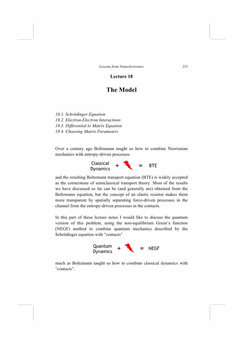
18.1. Schrödinger Equation 18.2. Electron-Electron Interactions 18.3. Differential to Matrix Equation 18.4. Choosing Matrix Parameters Over a century ago Boltzmann taught us how to combine Newtonian mechanics with entropy-driven processes and the resulting Boltzmann transport equation (BTE) is widely accepted as the cornerstone of semiclassical transport theory. Most of the results we have discussed so far can be (and generally are) obtained from the Boltzmann equation, but the concept of an elastic resistor makes them more transparent by spatially separating force-driven processes in the channel from the entropy-driven processes in the contacts. In this part of these lecture notes I would like to discuss the quantum version of this problem, using the non-equilibrium Green’s function (NEGF) method to combine quantum mechanics described by the Schrödinger equation with "contacts" much as Boltzmann taught us how to combine classical dynamics with "contacts".
The Model
253
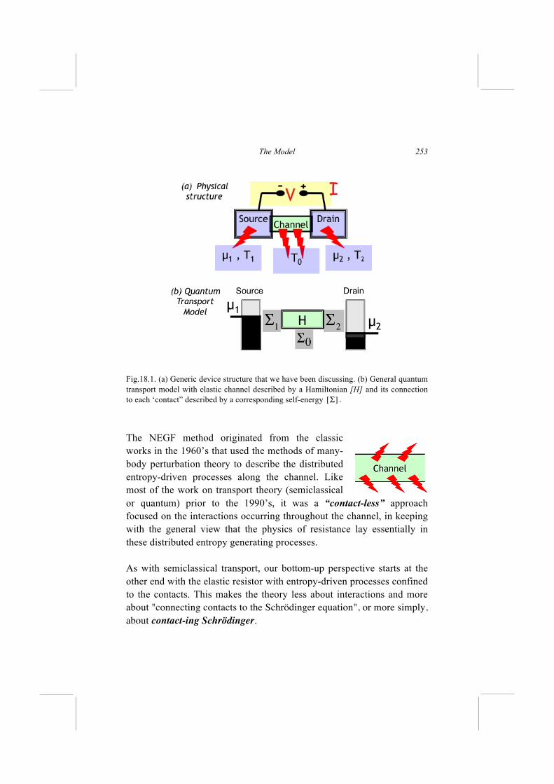
Fig.18.1. (a) Generic device structure that we have been discussing. (b) General quantum transport model with elastic channel described by a Hamiltonian [H] and its connection to each ‘contact” described by a corresponding self-energy [Σ] . The NEGF method originated from the classic works in the 1960’s that used the methods of many-body perturbation theory to describe the distributed entropy-driven processes along the channel. Like most of the work on transport theory (semiclassical or quantum) prior to the 1990’s, it was a “contact-less” approach focused on the interactions occurring throughout the channel, in keeping with the general view that the physics of resistance lay essentially in these distributed entropy generating processes. As with semiclassical transport, our bottom-up perspective starts at the other end with the elastic resistor with entropy-driven processes confined to the contacts. This makes the theory less about interactions and more about "connecting contacts to the Schrödinger equation", or more simply, about contact-ing Schrödinger.
Lessons from Nanoelectronics
254
But let me put off talking about the NEGF model till the next Lecture, and use subsequent lectures to illustrate its application to interesting problems in quantum transport. As indicated in Fig.18.1b the NEGF method requires two types of inputs: the Hamiltonian, [H] describing the dynamics of an elastic channel, and the self-energy [Σ] describing the connection to the contacts, using the word “contacts” in a broad figurative sense to denote all kinds of entropy-driven processes. Some of these contacts are physical like the ones labeled “1” and “2” in Fig.18.1b, while some are conceptual like the one labeled “0” representing entropy changing processes distributed throughout the channel. In this Lecture let me just try to provide a super-brief but self-contained introduction to how one writes down the Hamiltonian [H]. The [Σ] can be obtained by imposing the appropriate boundary conditions and will be described in later Lectures when we look at specific examples applying the NEGF method. We will try to describe the procedure for writing down [H] so that it is accessible even to those who have not had the benefit of a traditional multi-semester introduction to quantum mechanics. Moreover, our emphasis here is on something that may be helpful even for those who have this formal background. Let me explain. Most people think of the Schrödinger equation as a differential equation which is the form we see in most textbooks. However, practical calculations are usually based on a discretized version that represents the differential equation as a matrix equation involving the Hamiltonian matrix [H] of size NxN, N being the number of “basis functions” used to represent the structure. This matrix [H] can be obtained from first principles, but a widely used approach is to represent it in terms of a few parameters which are chosen to match key experiments. Such semi-empirical approaches are often used because of their convenience and because they can often explain a wide range of experiments beyond the key ones that are used as input, suggesting that they capture a lot of essential physics.
The Model
255
In order to follow the rest of the Lectures it is important for the readers to get a feeling for how one writes down this matrix [H] given an accepted energy-momentum E(p) relation (Lecture 5) for the material that is believed to describe the dynamics of conduction electrons with energies around the electrochemical potential. But I should stress that the NEGF framework we will talk about in subsequent lectures goes far beyond any specific model that we may choose to use for [H]. The same equations could be (and have been) used to describe say conduction through molecular conductors using first principles Hamiltonians.
18.1. Schrödinger Equation
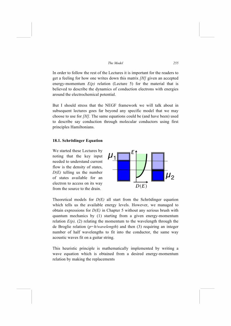
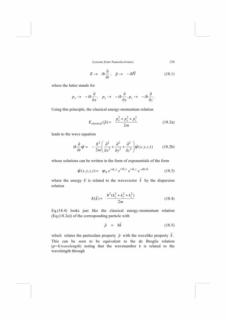
We started these Lectures by noting that the key input needed to understand current flow is the density of states, D(E) telling us the number of states available for an electron to access on its way from the source to the drain. Theoretical models for D(E) all start from the Schrödinger equation which tells us the available energy levels. However, we managed to obtain expressions for D(E) in Chapter 5 without any serious brush with quantum mechanics by (1) starting from a given energy-momentum relation E(p), (2) relating the momentum to the wavelength through the de Broglie relation (p=h/wavelength) and then (3) requiring an integer number of half wavelengths to fit into the conductor, the same way acoustic waves fit on a guitar string. This heuristic principle is mathematically implemented by writing a wave equation which is obtained from a desired energy-momentum relation by making the replacements
Lessons from Nanoelectronics
256
E→ i∂
∂t,p→ − i
∇ (18.1)
where the latter stands for
px → − i∂
∂x, py → − i
∂
∂y, pz → − i
∂
∂z,
Using this principle, the classical energy-momentum relation
Eclassical (p) =
px2+ py
2+ pz
2
2m (18.2a)
leads to the wave equation
i∂∂tψ = −
2
2m
∂2
∂x2+
∂2
∂y2+
∂2
∂z2⎛
⎝⎜⎞
⎠⎟ψ (x, y,z,t) (18.2b)
whose solutions can be written in the form of exponentials of the form
ψ (x, y,z,t) = ψ 0 e
+ikxxe+ik
yye+ik
zze−iEt / (18.3)
where the energy E is related to the wavevector k by the dispersion
relation
E(k ) =
2(kx2+ ky
2+ kz
2)
2m (18.4)
Eq.(18.4) looks just like the classical energy-momentum relation (Eq.(18.2a)) of the corresponding particle with
p =
k (18.5)
which relates the particulate property
p with the wavelike property
k .
This can be seen to be equivalent to the de Broglie relation (p=h/wavelength) noting that the wavenumber k is related to the wavelength through
The Model
257
k =2π
wavelength
The principle embodied in Eq.(18.1) ensures that the resulting wave equation has a group velocity that is the same as the velocity of the corresponding particle
1
∇kE
Wavegroup velocity
=
∇ pE
Particlevelocity
18.1.1. Spatially Varying Potential
The wave equation Eq.(18.2b) obtained from the energy-momentum relation describes free electrons. If there is a force described by a potential energy U(
r ) so that the classical energy is given by
Eclassical (r ,p) =
px2+ py
2+ pz
2
2m+ U(x, y,z) (18.6a)
then the corresponding wave equation has an extra term due to U( r )
i∂
∂tψ = −
2
2m∇2 ψ + U(
r ) ψ (18.6b)
where
r ≡ (x, y,z) and the Laplacian operator is defined as
∇2≡
∂2
∂x2+
∂2
∂y2+
∂2
∂z2
Solutions to Eq.(18.6b) can be written in the form
ψ (r ,t) = ψ (
r ) e
−iEt /
where ψ (r ) obeys the time-independent Schrödinger equation
Eψ (r ) = Hopψ (
r ) (18.7a)
Lessons from Nanoelectronics
258
where Hop is a differential operator obtained from the classical energy function in Eq.(18.6a), using the replacement mentioned earlier (Eq.(18.1)):
Hop = −2
2m∇2+ U(
r ) (18.7b)
Quantum mechanics started in the early twentieth century with an effort to “understand” the energy levels of the hydrogen atom deduced from the experimentally observed spectrum of the light emitted from an incandescent source. For a hydrogen atom Schrödinger used the potential energy
U(r ) = − Z
q2
4π ε0r
where the atomic number Z = 1, due to a point nucleus with charge +q , and solved Eq.(18.7) analytically for the allowed energy values En (called the eigenvalues of the operator Hop) given by
En = −Z2
n2
q2
8π ε0a0 (18.8)
with
a0 =4π ε0
2
mq2
and the corresponding solutions
ψnm (r ) = R
n(r )Y
m(θ ,φ)
obeying the equation
Enψ nm = −2
2m∇2 −
Zq2
4πε0r
⎛
⎝⎜⎞
⎠⎟ψ nm (
r )
The Model
259
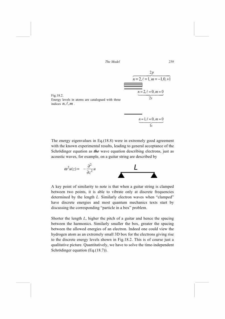
Fig.18.2. Energy levels in atoms are catalogued with three indices .
The energy eigenvalues in Eq.(18.8) were in extremely good agreement with the known experimental results, leading to general acceptance of the Schrödinger equation as the wave equation describing electrons, just as acoustic waves, for example, on a guitar string are described by
ω 2u(z) = −
∂2
∂z2u
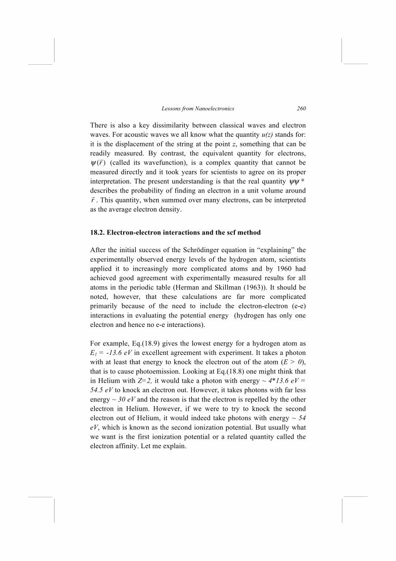
A key point of similarity to note is that when a guitar string is clamped between two points, it is able to vibrate only at discrete frequencies determined by the length L. Similarly electron waves when “clamped” have discrete energies and most quantum mechanics texts start by discussing the corresponding “particle in a box” problem. Shorter the length L, higher the pitch of a guitar and hence the spacing between the harmonics. Similarly smaller the box, greater the spacing between the allowed energies of an electron. Indeed one could view the hydrogen atom as an extremely small 3D box for the electrons giving rise to the discrete energy levels shown in Fig.18.2. This is of course just a qualitative picture. Quantitatively, we have to solve the time-independent Schrödinger equation (Eq.(18.7)).
n,,m
Lessons from Nanoelectronics
260
There is also a key dissimilarity between classical waves and electron waves. For acoustic waves we all know what the quantity u(z) stands for: it is the displacement of the string at the point z, something that can be readily measured. By contrast, the equivalent quantity for electrons,
ψ (r ) (called its wavefunction), is a complex quantity that cannot be
measured directly and it took years for scientists to agree on its proper interpretation. The present understanding is that the real quantity ψψ *describes the probability of finding an electron in a unit volume around
r . This quantity, when summed over many electrons, can be interpreted as the average electron density.
18.2. Electron-electron interactions and the scf method
After the initial success of the Schrödinger equation in “explaining” the experimentally observed energy levels of the hydrogen atom, scientists applied it to increasingly more complicated atoms and by 1960 had achieved good agreement with experimentally measured results for all atoms in the periodic table (Herman and Skillman (1963)). It should be noted, however, that these calculations are far more complicated primarily because of the need to include the electron-electron (e-e) interactions in evaluating the potential energy (hydrogen has only one electron and hence no e-e interactions). For example, Eq.(18.9) gives the lowest energy for a hydrogen atom as E1 = -13.6 eV in excellent agreement with experiment. It takes a photon with at least that energy to knock the electron out of the atom (E > 0), that is to cause photoemission. Looking at Eq.(18.8) one might think that in Helium with Z=2, it would take a photon with energy ~ 4*13.6 eV = 54.5 eV to knock an electron out. However, it takes photons with far less energy ~ 30 eV and the reason is that the electron is repelled by the other electron in Helium. However, if we were to try to knock the second electron out of Helium, it would indeed take photons with energy ~ 54 eV, which is known as the second ionization potential. But usually what we want is the first ionization potential or a related quantity called the electron affinity. Let me explain.
The Model
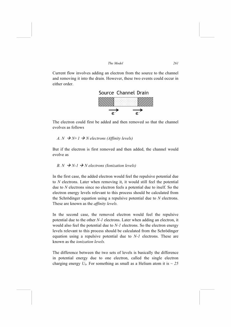
261
Current flow involves adding an electron from the source to the channel and removing it into the drain. However, these two events could occur in either order. The electron could first be added and then removed so that the channel evolves as follows A. N N+1 N electrons (Affinity levels) But if the electron is first removed and then added, the channel would evolve as B. N N-1 N electrons (Ionization levels) In the first case, the added electron would feel the repulsive potential due to N electrons. Later when removing it, it would still feel the potential due to N electrons since no electron feels a potential due to itself. So the electron energy levels relevant to this process should be calculated from the Schrödinger equation using a repulsive potential due to N electrons. These are known as the affinity levels. In the second case, the removed electron would feel the repulsive potential due to the other N-1 electrons. Later when adding an electron, it would also feel the potential due to N-1 electrons. So the electron energy levels relevant to this process should be calculated from the Schrödinger equation using a repulsive potential due to N-1 electrons. These are known as the ionization levels. The difference between the two sets of levels is basically the difference in potential energy due to one electron, called the single electron charging energy U0. For something as small as a Helium atom it is ~ 25
Lessons from Nanoelectronics
262
eV, so large that it is hard to miss. For large conductors it is often so small that it can be ignored, and it does not matter too much whether we use the potential due to N electrons or due to N-1 electrons. For small conductors, under certain conditions the difference can be important giving rise to single-electron charging effects, which we will ignore for the moment and take up again later in Lecture 24. Virtually all the progress that has been made in understanding "condensed matter," has been based on the self-consistent field (scf) method where we think of each electron as behaving quasi-independently feeling an average self-consistent potential
U(r ) due to all the other
electrons in addition to the nuclear potential. This potential depends on the electron density
n(r ) which in turn is determined by the
wavefunctions of the filled states. Given the electron density how one determines
U(r ) is the subject of much discussion and research. The
“zero order” approach is to calculate U(r ) from
n(r ) based on the laws
of electrostatics, but it is well-established that this so-called Hartree approximation will overestimate the repulsive potential and there are various approaches for estimating this reduction. The density functional theory (DFT) has been spectacularly successful in describing this correction for equilibrium problems and in its simplest form amounts to a reduction by an amount proportional to the cube root of the electron density
U(r ) = UHartree −
q2
4πεn(r )( )
1/3
(18.9)
Many are now using similar corrections for non-equilibrium problems like current flow as well, though we believe there are important issues that remain to be resolved. We should also note that there is a vast literature (both experiment and theory) on a regime of transport that cannot be easily described within an scf model. It is not just a matter of correctly evaluating the self-consistent potential. The very picture of quasi-independent electrons
The Model
263
moving in a self-consistent field needs revisiting, as we will see in Lecture 23.
18.3. Differential to Matrix Equation
All numerical calculations typically proceed by turning the differential equation in Eq.(18.11) into a matrix equation of the form
(18.10)
or equivalently
by expanding the wavefunction in terms of a set of known functions um(r) called the basis functions:
ψ (r ) = ψ
mum(r )
m
∑ (18.11a)
The elements of the two matrices [S] and [H] are given respectively by
Snm = d
r un
*(r )um (
r )∫
Hnm = d
r un
*(r )Hop um (
r )∫ (18.11b)
These expressions are of course by no means obvious, but we will not go into it further since we will not really be making any use of them. Let me explain why.
18.3.1. Semi-empirical tight-binding (TB) models
There are a wide variety of techniques in use which differ in the specific basis functions they use to convert the differential equation into a matrix equation. But once the matrices [S] and [H] have been evaluated, the eigenvalues E of Eq.(18.10) (which are the allowed energy levels) are determined using powerful matrix techniques that are widely available.
E[S] ψ{ } = [H ] ψ{ }
E Snm
m
∑ ψm
= Hnm
m
∑ ψm
Lessons from Nanoelectronics
264
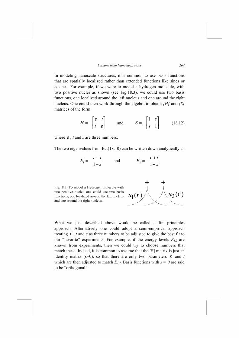
In modeling nanoscale structures, it is common to use basis functions that are spatially localized rather than extended functions like sines or cosines. For example, if we were to model a hydrogen molecule, with two positive nuclei as shown (see Fig.18.3), we could use two basis functions, one localized around the left nucleus and one around the right nucleus. One could then work through the algebra to obtain [H] and [S] matrices of the form
and (18.12)
where , t and s are three numbers. The two eigenvalues from Eq.(18.10) can be written down analytically as
and
Fig.18.3. To model a Hydrogen molecule with two positive nuclei, one could use two basis functions, one localized around the left nucleus and one around the right nucleus. What we just described above would be called a first-principles approach. Alternatively one could adopt a semi-empirical approach treating , t and s as three numbers to be adjusted to give the best fit to our “favorite” experiments. For example, if the energy levels E1,2 are known from experiments, then we could try to choose numbers that match these. Indeed, it is common to assume that the [S] matrix is just an identity matrix (s=0), so that there are only two parameters and t which are then adjusted to match E1,2. Basis functions with s = 0 are said to be “orthogonal.”
H =ε t
t ε
⎡
⎣⎢
⎤
⎦⎥ S =
1 s
s 1
⎡
⎣⎢
⎤
⎦⎥
ε
E1=
ε − t
1− sE2=
ε + t
1+ s
ε
ε
The Model
265
18.3.2. Size of matrix, N = n*b
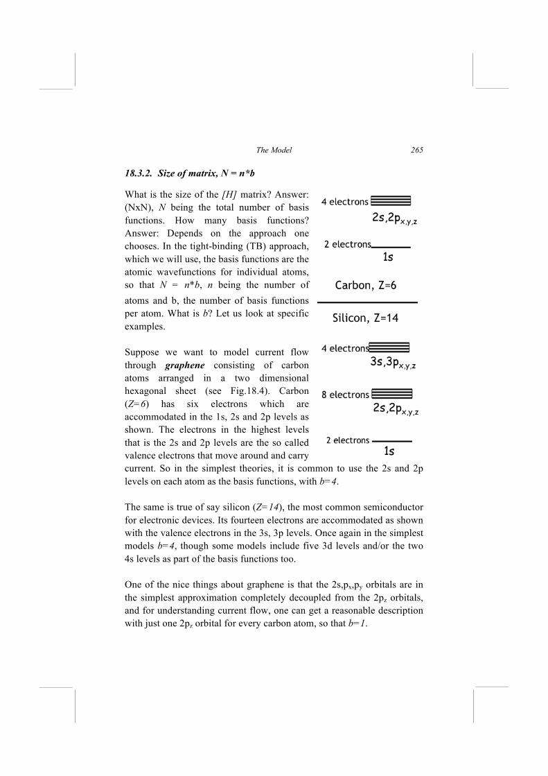
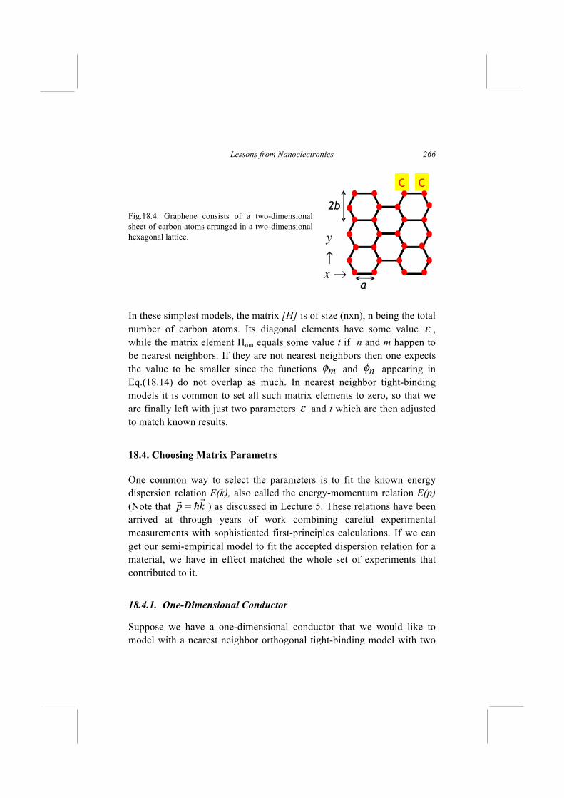
What is the size of the [H] matrix? Answer: (NxN), N being the total number of basis functions. How many basis functions? Answer: Depends on the approach one chooses. In the tight-binding (TB) approach, which we will use, the basis functions are the atomic wavefunctions for individual atoms, so that N = n*b, n being the number of atoms and b, the number of basis functions per atom. What is b? Let us look at specific examples. Suppose we want to model current flow through graphene consisting of carbon atoms arranged in a two dimensional hexagonal sheet (see Fig.18.4). Carbon (Z=6) has six electrons which are accommodated in the 1s, 2s and 2p levels as shown. The electrons in the highest levels that is the 2s and 2p levels are the so called valence electrons that move around and carry current. So in the simplest theories, it is common to use the 2s and 2p levels on each atom as the basis functions, with b=4. The same is true of say silicon (Z=14), the most common semiconductor for electronic devices. Its fourteen electrons are accommodated as shown with the valence electrons in the 3s, 3p levels. Once again in the simplest models b=4, though some models include five 3d levels and/or the two 4s levels as part of the basis functions too. One of the nice things about graphene is that the 2s,px,py orbitals are in the simplest approximation completely decoupled from the 2pz orbitals, and for understanding current flow, one can get a reasonable description with just one 2pz orbital for every carbon atom, so that b=1.
Lessons from Nanoelectronics
266
Fig.18.4. Graphene consists of a two-dimensional sheet of carbon atoms arranged in a two-dimensional hexagonal lattice. In these simplest models, the matrix [H] is of size (nxn), n being the total number of carbon atoms. Its diagonal elements have some value , while the matrix element Hnm equals some value t if n and m happen to be nearest neighbors. If they are not nearest neighbors then one expects the value to be smaller since the functions and appearing in Eq.(18.14) do not overlap as much. In nearest neighbor tight-binding models it is common to set all such matrix elements to zero, so that we are finally left with just two parameters and t which are then adjusted to match known results.
18.4. Choosing Matrix Parametrs
One common way to select the parameters is to fit the known energy dispersion relation E(k), also called the energy-momentum relation E(p) (Note that ) as discussed in Lecture 5. These relations have been arrived at through years of work combining careful experimental measurements with sophisticated first-principles calculations. If we can get our semi-empirical model to fit the accepted dispersion relation for a material, we have in effect matched the whole set of experiments that contributed to it.
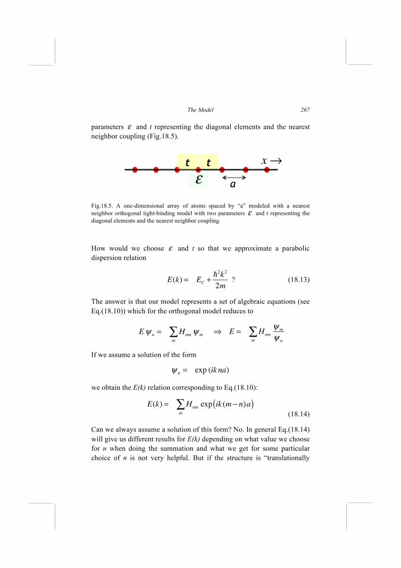
18.4.1. One-Dimensional Conductor
Suppose we have a one-dimensional conductor that we would like to model with a nearest neighbor orthogonal tight-binding model with two
ε
φm φn
ε
p =
k
The Model
267
parameters and t representing the diagonal elements and the nearest neighbor coupling (Fig.18.5).
Fig.18.5. A one-dimensional array of atoms spaced by “a” modeled with a nearest neighbor orthogonal tight-binding model with two parameters and t representing the diagonal elements and the nearest neighbor coupling. How would we choose and t so that we approximate a parabolic dispersion relation
? (18.13)
The answer is that our model represents a set of algebraic equations (see Eq.(18.10)) which for the orthogonal model reduces to
If we assume a solution of the form
we obtain the E(k) relation corresponding to Eq.(18.10):
(18.14)
Can we always assume a solution of this form? No. In general Eq.(18.14) will give us different results for E(k) depending on what value we choose for n when doing the summation and what we get for some particular choice of n is not very helpful. But if the structure is “translationally
ε
ε
ε
E(k) = EC+2k2
2m
Eψn= H
nm
m
∑ ψm
⇒ E = Hnm
m
∑ψ
m
ψn
ψn= exp (ik na)
E(k) = Hnm
m
∑ exp ik (m − n)a( )
Lessons from Nanoelectronics
268
invariant” such that we get the same answer for all n then we get a unique E(k) relation and Eq.(18.13) indeed represents an acceptable solution to our set of equations. For our particular nearest neighbor model Eq.(18.14) yields straightforwardly
(18.15)
How would we make this match the desired parabolic relation in Eq.(18.13) ? Clearly one could not match them for all values of k, only for a limited range. For example, if we want them to match over a range of k-values around k=0, we can expand the cosine in a Taylor series around ka = 0 to write
so that the best match is obtained by choosing
and (18.16)
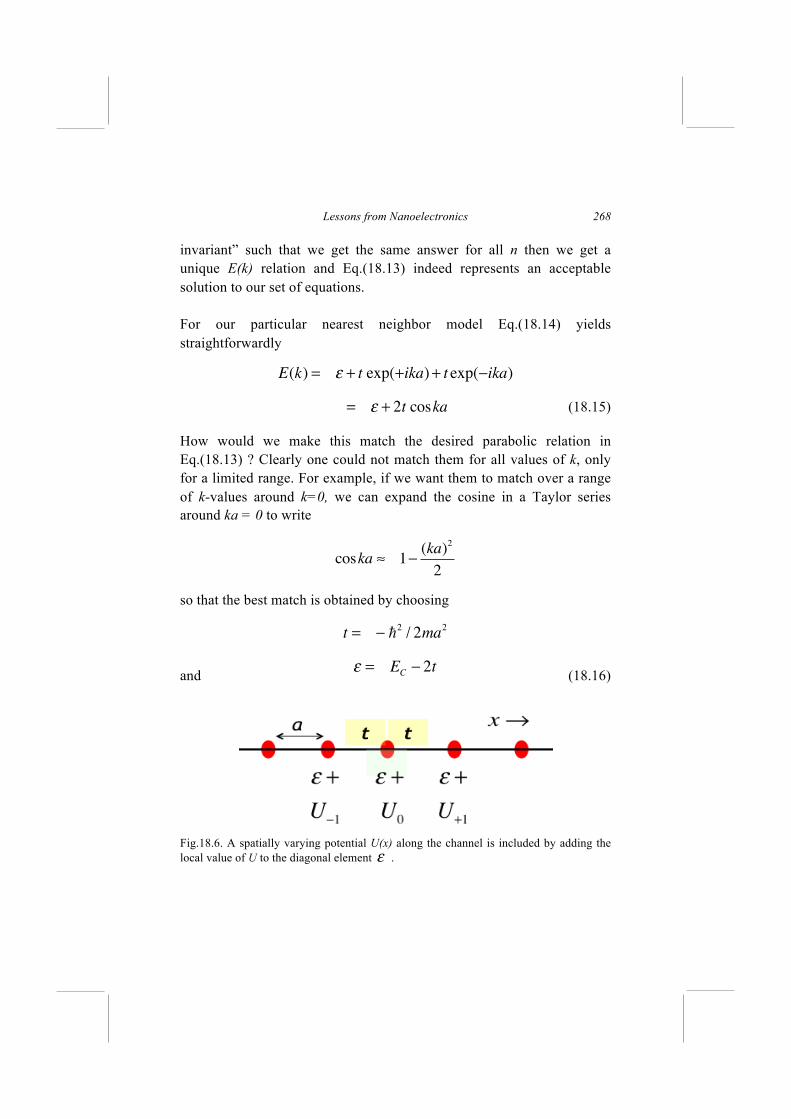
Fig.18.6. A spatially varying potential U(x) along the channel is included by adding the local value of U to the diagonal element .
E(k) = ε + t exp(+ika)+ t exp(−ika)
= ε + 2t coska
coska ≈ 1−(ka)
2
2
t = − 2/ 2ma
2
ε = EC− 2t
ε
The Model
269
Finally I should mention that when modeling a device there could be a spatially varying potential U(x) along the channel which is included by adding the local value of U to the diagonal element as indicated in Fig.18.6. We now no longer have the “translational invariance” needed for a solution of the form exp(ikx) and the concept of a dispersion relation E(k) is not valid. But a Hamiltonian of the form just described (Fig.18.6) can be used for numerical calculations and appear to be fairly accurate at least for potentials U(x) that do not vary too rapidly on an atomic scale.
18.4.2. Two-Dimensional Conductor
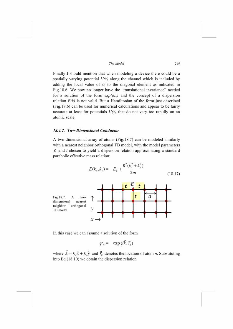
A two-dimensional array of atoms (Fig.18.7) can be modeled similarly with a nearest neighbor orthogonal TB model, with the model parameters
and t chosen to yield a dispersion relation approximating a standard parabolic effective mass relation:
(18.17)
Fig.18.7. A two-dimensional nearest neighbor orthogonal TB model.
In this case we can assume a solution of the form
where and denotes the location of atom n. Substituting into Eq.(18.10) we obtain the dispersion relation
ε
E(kx,ky ) = EC +2(kx
2+ ky
2)
2m
ψn= exp (i
k.rn)
k = kx x + ky y
rn
Lessons from Nanoelectronics
270
(18.18a)
which for our nearest neighbor model yields
(18.18b)
Following the same arguments as in the 1-D case, we can make this match the parabolic relation in Eq.(18.17) by choosing
(18.19)
18.4.3. TB parameters in B-field
It is shown in Appendix C that if we replace
p with
p + q
A in
Eq.(18.6a)
Eclassical (r ,p) =
(p + q
A).(p + q
A)
2m+ U(
r )
yields the correct classical laws of motion of a particle of charge –q in a vector potential
A . The corresponding wave equation is obtained using
the replacement in Eq.(18.1):
p→− i
∇ .
To find the appropriate TB parameters for the Hamiltonian in a B-field we consider the homogeneous material with constant Ec and a constant vector potential. Consider first the 1D problem with
E(px ) = Ec +(px + qAx )(px + qAx )
2m
so that the corresponding wave equation has a dispersion relation
E(k ) = H
nm
m
∑ exp ik.(rm−rn)( )
E(k ) = ε + t exp(+ikxa)+ t exp(−ikxa)
+ t exp(+ikya)+ t exp(−ikya)
= ε + 2t cos(kxa)+ 2t cos(kya)
t = − 2/ 2ma
2
ε = EC− 4t
The Model
271
E(kx ) = Ec +(kx + qAx )(kx + qAx )
2m
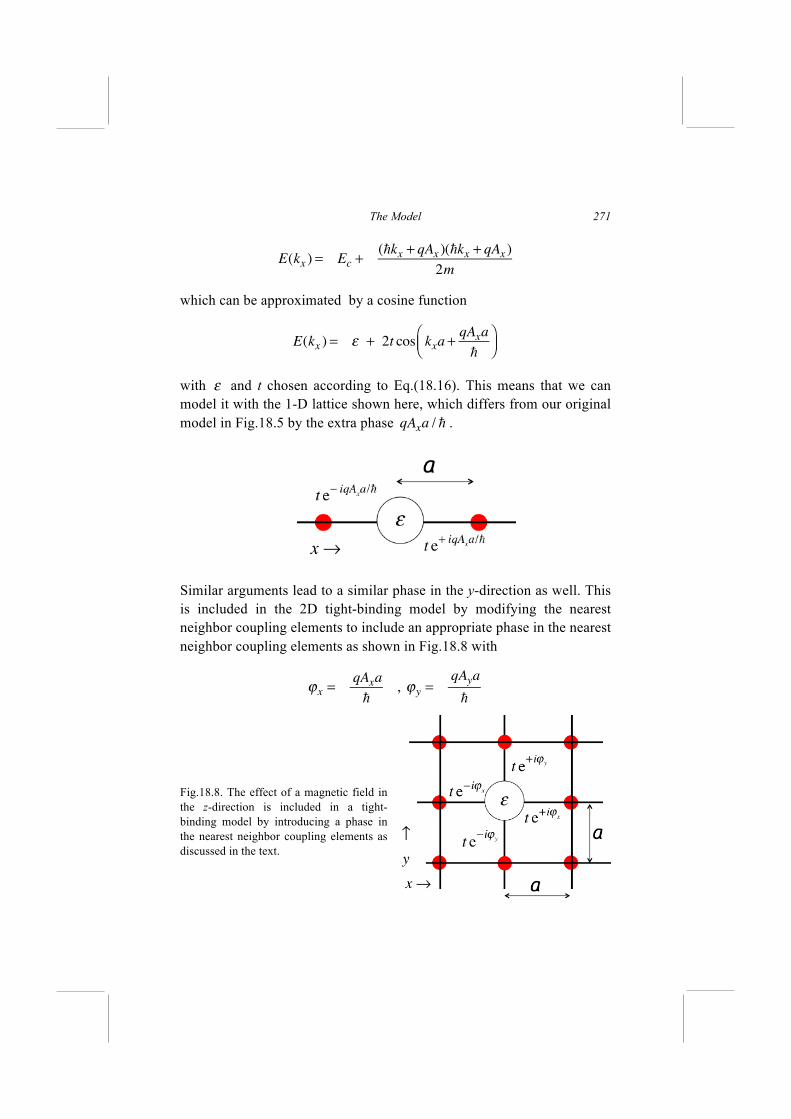
which can be approximated by a cosine function
E(kx ) = ε + 2t cos kxa +qAxa
⎛⎝⎜
⎞⎠⎟
with ε and t chosen according to Eq.(18.16). This means that we can model it with the 1-D lattice shown here, which differs from our original model in Fig.18.5 by the extra phase
qAxa / .
Similar arguments lead to a similar phase in the y-direction as well. This is included in the 2D tight-binding model by modifying the nearest neighbor coupling elements to include an appropriate phase in the nearest neighbor coupling elements as shown in Fig.18.8 with
ϕx =qAxa
,
ϕy =qAya
Fig.18.8. The effect of a magnetic field in the z-direction is included in a tight-binding model by introducing a phase in the nearest neighbor coupling elements as discussed in the text.
Lessons from Nanoelectronics
272
To include a B-field we have to let the vector potential vary spatially from one lattice point to the next such that
B =
∇×A
For example, a B-field in the z-direction described in general by a vector potential Ax(y) and/or Ay(x) such that
Bz =∂Ay
∂x−
∂Ax
∂y
For a given B-field the potential A is not unique, and it is usually convenient to choose a potential that does not vary along the direction of current flow.
18.4.4. Lattice with a “Basis”
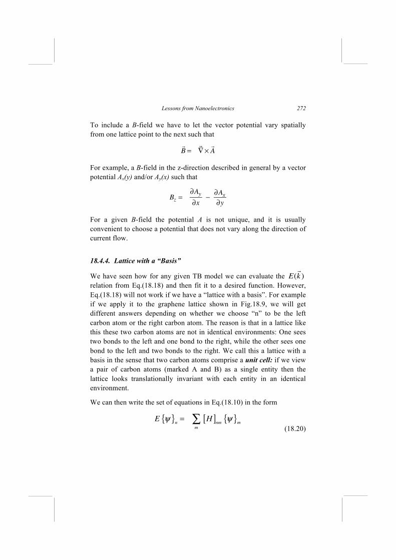
We have seen how for any given TB model we can evaluate the relation from Eq.(18.18) and then fit it to a desired function. However, Eq.(18.18) will not work if we have a “lattice with a basis”. For example if we apply it to the graphene lattice shown in Fig.18.9, we will get different answers depending on whether we choose “n” to be the left carbon atom or the right carbon atom. The reason is that in a lattice like this these two carbon atoms are not in identical environments: One sees two bonds to the left and one bond to the right, while the other sees one bond to the left and two bonds to the right. We call this a lattice with a basis in the sense that two carbon atoms comprise a unit cell: if we view a pair of carbon atoms (marked A and B) as a single entity then the lattice looks translationally invariant with each entity in an identical environment.
We can then write the set of equations in Eq.(18.10) in the form
(18.20)
E(k )
E ψ{ }n= H[ ]
nm
m
∑ ψ{ }m
The Model
273
where ψn{ } is a (2x1) column vector whose components represent the
two atoms comprising unit cell number n. Similarly [Hnm] is a (2x2) matrix representing the coupling between the two components of unit cell n and unit cell m (see Fig.18.9).
Fig.18.9: If we view two carbon atoms as a single entity then the lattice in Fig.18.4 looks translationally invariant with each entity in an identical environment. Viewing the two atoms in each unit cell as a single entity we can write the set of equations in the form shown in Eq.(18.20) with [H]nm given by (2x2) matrices as shown.
Now if we write the solution in the form
(18.21)
we obtain from Eq.(18.20)
(18.22)
where (18.23)
ψ{ }n= ψ{ }
0exp(i
k.rn)
E ψ{ }0= h(
k )⎡⎣ ⎤⎦ ψ{ }
0
h(k )⎡⎣ ⎤⎦ = [H ]
nm
m
∑ exp ik.(rm−rn)( )
Lessons from Nanoelectronics
274
Note that obtained from Eq.(18.23) is a (2x2) matrix, which can be shown after some algebra to be
(18.24)
where (18.25)
Eq.(18.22) yields two eigenvalues for the energy E for each value of :
(18.26)
Eq.(18.26) and (18.25) give a widely used dispersion relation for graphene. Once again to obtain a simple polynomial relation we need a Taylor series expansion around the k-value of interest. In this case the k-values of interest are those that make
,
so that
This is because the equilibrium electrochemical potential is located at for a neutral sample for which exactly half of all the energy levels given by Eq.(18.26) are occupied.
It is straightforward to see that this requires
(18.27)
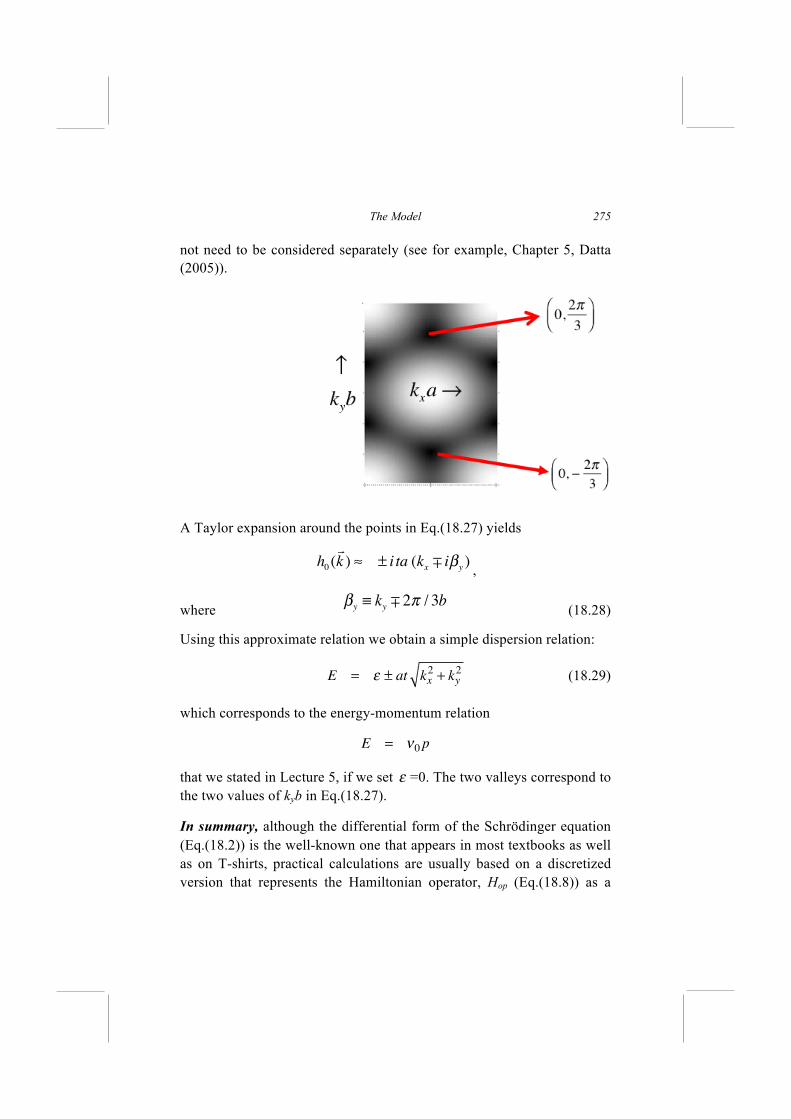
Alternatively one could numerically make a grayscale plot of the magnitude of
h0(k ) as shown below and look for the dark spots where it
is a minimum. Each of these spots is called a valley and one can do a Taylor expansion around the minimum to obtain an approximate dispersion relation valid for that valley. Note that two of the dark spots correspond to the points in Eq.(18.27), but there are other spots too and it requires some discussion to be convinced that these additional valleys do
[h(k )]
[h(k )] =
ε h0
*
h0
ε
⎡
⎣⎢
⎤
⎦⎥
h0 ≡ t (1+ 2cos(kyb) exp(+ikxa))
k
E(k ) = ε ± h
0(k )
h0(k ) = 0
E(k ) = ε
ε
h0(k ) = 0 → kxa = 0, kyb = ± 2π / 3
The Model
275
not need to be considered separately (see for example, Chapter 5, Datta (2005)).
A Taylor expansion around the points in Eq.(18.27) yields
,
where (18.28)
Using this approximate relation we obtain a simple dispersion relation:
E = ε ± at kx2+ ky
2 (18.29)
which corresponds to the energy-momentum relation
E = ν0p
that we stated in Lecture 5, if we set ε =0. The two valleys correspond to the two values of kyb in Eq.(18.27).
In summary, although the differential form of the Schrödinger equation (Eq.(18.2)) is the well-known one that appears in most textbooks as well as on T-shirts, practical calculations are usually based on a discretized version that represents the Hamiltonian operator, Hop (Eq.(18.8)) as a
h0(k ) ≈ ± i ta (kx iβy )
βy ≡ ky 2π / 3b
Lessons from Nanoelectronics
276
matrix of size NxN, N being the number of basis functions used to represent the structure. Given a set of basis functions, the matrix [H] can be obtained from first principles, but a widely used approach is to use the principles of bandstructure to represent the matrix in terms of a few parameters which are chosen to match key experiments. Such semi-empirical approaches are often used because of their convenience and can explain a wide range of experiments beyond the key ones used that are used as input, suggesting that they capture a lot of essential physics. Our approach in these Lectures will be to
(1) take accepted energy-momentum E(p) relations that are believed to describe the dynamics of conduction electrons with energies around the electrochemical potential µ0 ,
(2) extract appropriate parameters to use in tight-binding model by discretizing it.
Knowing the [H], we can obtain the [Σ1,2 ] describing the connection to
the physical contacts and possible approaches will be described when discussing specific examples in Lectures 20 through 22. A key difference between the [H] and [Σ] matrices is that the former is Hermitian with real eigenvalues, while the latter is non-Hermitian with complex eigenvalues, whose significance we will discuss in the next Lecture.
As we mentioned at the outset, there are many approaches to writing [H] and [Σ1,2 ] of which we have only described the simplest versions. But
regardless of how we chose to write these matrices, we can use the NEGF-based approach to be described in the next Lecture.
NEGF Method
277
Lecture 19
NEGF Method
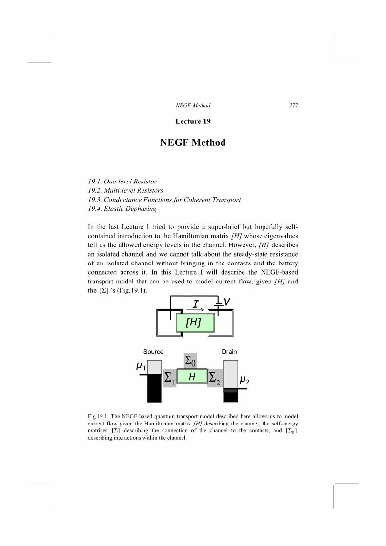
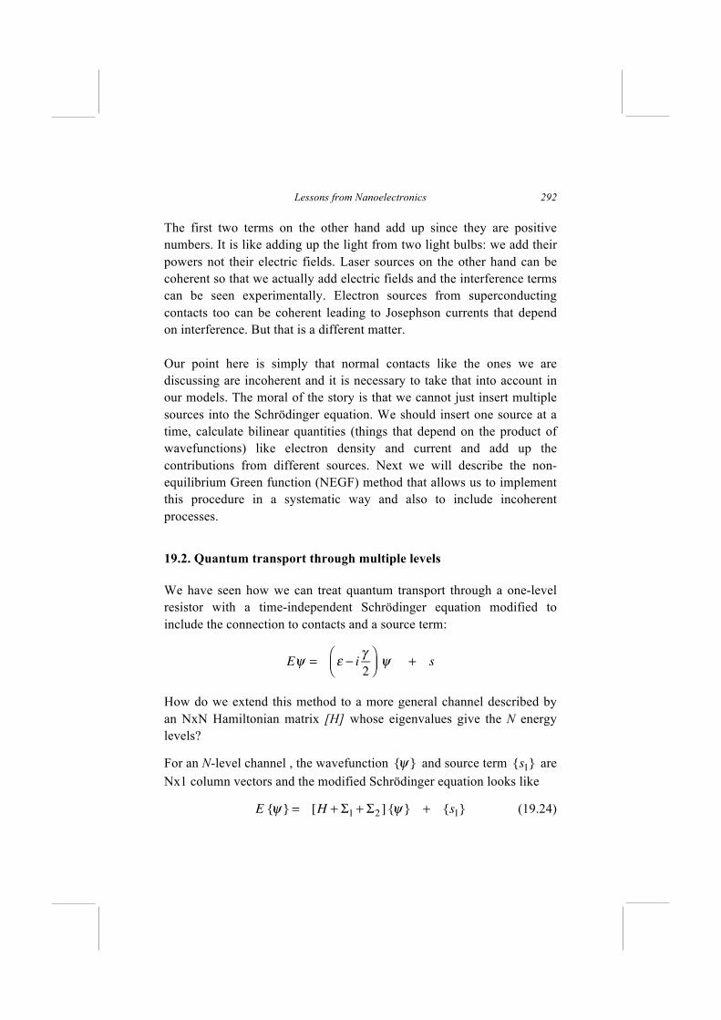
19.1. One-level Resistor 19.2. Multi-level Resistors 19.3. Conductance Functions for Coherent Transport 19.4. Elastic Dephasing In the last Lecture I tried to provide a super-brief but hopefully self-contained introduction to the Hamiltonian matrix [H] whose eigenvalues tell us the allowed energy levels in the channel. However, [H] describes an isolated channel and we cannot talk about the steady-state resistance of an isolated channel without bringing in the contacts and the battery connected across it. In this Lecture I will describe the NEGF-based transport model that can be used to model current flow, given [H] and the [Σ] ’s (Fig.19.1). Fig.19.1. The NEGF-based quantum transport model described here allows us to model current flow given the Hamiltonian matrix [H] describing the channel, the self-energy matrices [Σ] describing the connection of the channel to the contacts, and [Σ0 ] describing interactions within the channel.
Lessons from Nanoelectronics
278
As I mentioned in Lectures 1 and 18, the NEGF method originated from the seminal works of Martin and Schwinger (1959), Kadanoff and Baym (1962), Keldysh (1965) and others who used the methods of many-body perturbation theory (MBPT) to describe the distributed entropy-generating processes along the channel which were believed to constitute the essence of resistance. Since MBPT is an advanced topic requiring many semesters to master, the NEGF method is generally regarded as an esoteric tool for specialists. In our bottom-up approach we will start with elastic resistors for which energy exchange is confined to the contacts, and the problem of resistance can be treated within a one-electron picture by connecting contacts to the Schrödinger equation. Indeed our approach will be to start from the usual time-independent Schrödinger equation E {ψ } = [H ] {ψ } and add two terms to it representing the outflow and inflow from the contact
E {ψ } = [H ] {ψ } + [Σ] {ψ }
OUTFLOW
+ {s}
INFLOW
These two terms arise from imposing open boundary conditions on the Schrödinger equation with an incident wave from the contact as shown in Chapters 8,9 of Datta (2005). Some readers may notice the similarity of the additional terms here with those appearing in the Langevin equation used to describe Brownian motion, but we will not go into it. Using this modified Schrödinger equation, the wavefunction can be written as
ψ{ } = [EI − H − Σ] −1 {s}
We will then argue that since the inflow from multiple sources {s} are incoherent, one cannot superpose the resulting {ψ }’s and it is more convenient to work in terms of quantities like (superscript ‘+’ denotes conjugate transpose)
NEGF Method
279
[Gn] ~ {ψ }{ψ }+
[Σin] ~ {s} {s}
+
which can be superposed. Defining
GR
= [EI − H − Σ]−1 (19.1)
and GA= [G
R]+
we can write ψ{ } = [GR] {s}
so that
ψ{ } ψ{ }+
Gn
= [G
R] {s} {s}
+
Σ in
[G
A]
giving us the second NEGF equation
Gn
= GRΣinGA (19.2)
Though we have changed the notation somewhat, writing Σ for ΣR , and (see Chapter 8, Datta 1995)
Gnfor − iG
< and Σin for − iΣ<
Eqs.(19.1, 19.2) are essentially the same as Eqs.(75-77) in Keldysh (1965), which is one of the seminal founding papers on the NEGF method that obtained these equations using MBPT. Although for simplicity we have only discussed the time-independent version here, a similar derivation could be used for the time-dependent version too (See Appendix, Datta (2005)). How could we obtain these results using elementary arguments, without invoking MBPT? Because we are dealing with an elastic resistor where all entropy-generating processes are confined to the contacts and can be handled in a relatively elementary manner. But should we call this NEGF?
Lessons from Nanoelectronics
280
It seems to us that NEGF has two aspects, namely A. Eqs.(19.1), (19.2) and B. calculating [Σ] , [Σin ] that appear in Eqs.(19.1), (19.2).
For historical reasons, these two aspects, A and B, are often intertwined in the literature, but they need not be. Indeed these two aspects are completely distinct in the Boltzmann formalim (Lecture 7). The Boltzmann transport equation (BTE)
∂ f
∂t+ν .∇f +
F.∇ p f = Sop f (same as Eq.(7.5))
is used to describe semiclassical transport in many different contexts, but the evaluation of the scattering operator Sop has evolved considerably since the days of Boltzmann and varies widely depending on the problem at hand. Similarly it seems to me that the essence of NEGF is contained in Eqs.(19.1), (19.2) while the actual evaluation of the [Σ] ’s may well evolve as we look at more and more different types of problems. The original MBPT–based approach may or may not be the best, and may need to be modified even for problems involving electron-electron interactions. Above all we believe that by decoupling Eqs.(19.1) and (19.2) from the MBPT method originally used to derive them, we can make the NEGF method more transparent and accessible so that it can become a part of the standard training of physics and engineering students who need to apply it effectively to a wide variety of basic and applied problems that require connecting contacts to the Schrödinger equation.
I should also note briefly the relation between the NEGF method applied to elastic resistors with the scattering theory of transport or the transmission formalism widely used in mesoscopic physics. Firstly, the scattering theory works directly with the Schrödinger equation with open
NEGF Method
281
boundary conditions that effectively add the inflow and outflow terms we mentioned:
E {ψ } = [H ] {ψ } + [Σ] {ψ }
OUTFLOW
+ {s}
INFLOW
However, as we noted earlier it is then important to add individual sources incoherently, something that the NEGF equation (Eq.(19.2)) takes care of automatically.
The second key difference is the handling of dephasing processes in the channel, something that has no classical equivalent. In quantum transport randomization of the phase of the wavefunction even without any momentum relaxation can have a major impact on the measured conductance. The scattering theory of transport usually neglects such dephasing processes and is restricted to phase-coherent elastic resistors. Incoherence is commonly introduced in this approach using an insightful observation due to Büttiker that dephasing processes essentially remove electrons from the channel and re-inject them just like the voltage probes discussed in Section 12.2 and so one can include them phenomenologically by introducing conceptual contacts in the channel. This method is widely used in mesoscopic physics, but it seems to introduce both phase and momentum relaxation and I am not aware of a convenient way to introduce pure phase relaxation if we wanted to. In the NEGF method it is straightforward to choose [ Σ0 ] so as to include phase relaxation with or without momentum relaxation as we will see in the next Lecture. In addition, the NEGF method provides a rigorous framework for handling all kinds of interactions in the channel, both elastic and inelastic, using MBPT. Indeed that is what the original work from the 1960’s was about.
Let me finish up this long introduction by briefly mentioning the two other key equations in NEGF besides Eqs.(19.1) and (19.2). As we will see, the quantity [Gn] appearing in Eq.(19.2) represents a matrix version of the electron density (times 2π ) from which other quantities of interest
Lessons from Nanoelectronics
282
can be calculated. Another quantity of interest is the matrix version of the density of states (again times 2π ) called the spectral function [A] given by
A = G
RΓG
A= G
AΓG
R
= i[GR−G
A]
(19.3a)
where GR, GA are defined in Eq.(19.1) and the [Γ] ’s represent the anti-Hermitian parts of the corresponding [Σ] ’s
Γ = i[Σ − Σ+] (19.3b)
which describe how easily the electrons in the channel communicate with the contacts. There is a component of [Σ] , [Γ] , [Σin ] for each contact (physical or otherwise) and the quantities appearing in Eqs.(19.1-19.3) are the total obtained summing all components. The current at a specific contact m, however, involves only those components associated with contact m:
Im =q
hTrace[Σm
inA − ΓmG
n] (19.4)
Note that Im(E) represents the current per unit energy and has to be
integrated over all energy to obtain the total current. In the following four Lectures we will look at a few examples designed to illustrate how Eqs.(19.1)-(19.4) are applied to obtain concrete results. But for the rest of this Lecture let me try to justify these equations. We start with a one-level version for which all matrices are just numbers (Section 19.1), then look at the full multi-level version (Section 19.2), obtain an expression for the conductance function G(E) for coherent transport (Section 19.3) and finally look at the different choices for the dephasing self-energy [ Σ0 ] (Section 19.4).
NEGF Method
283
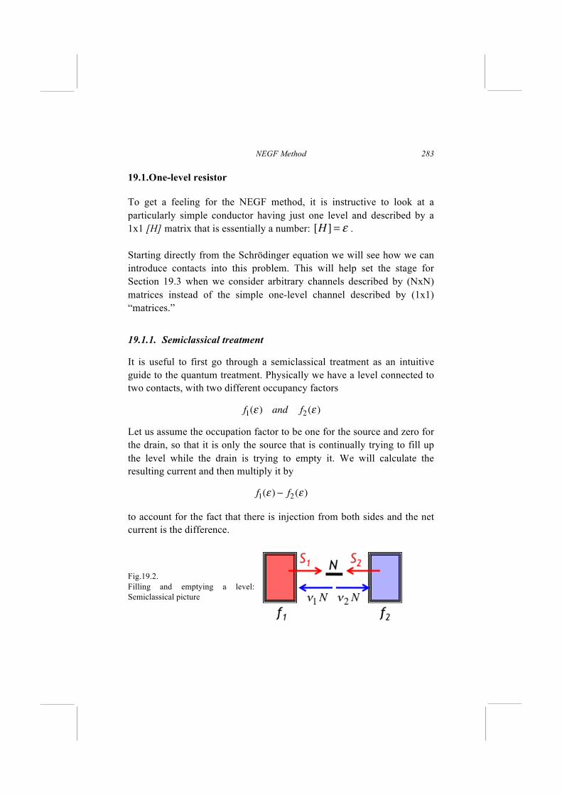
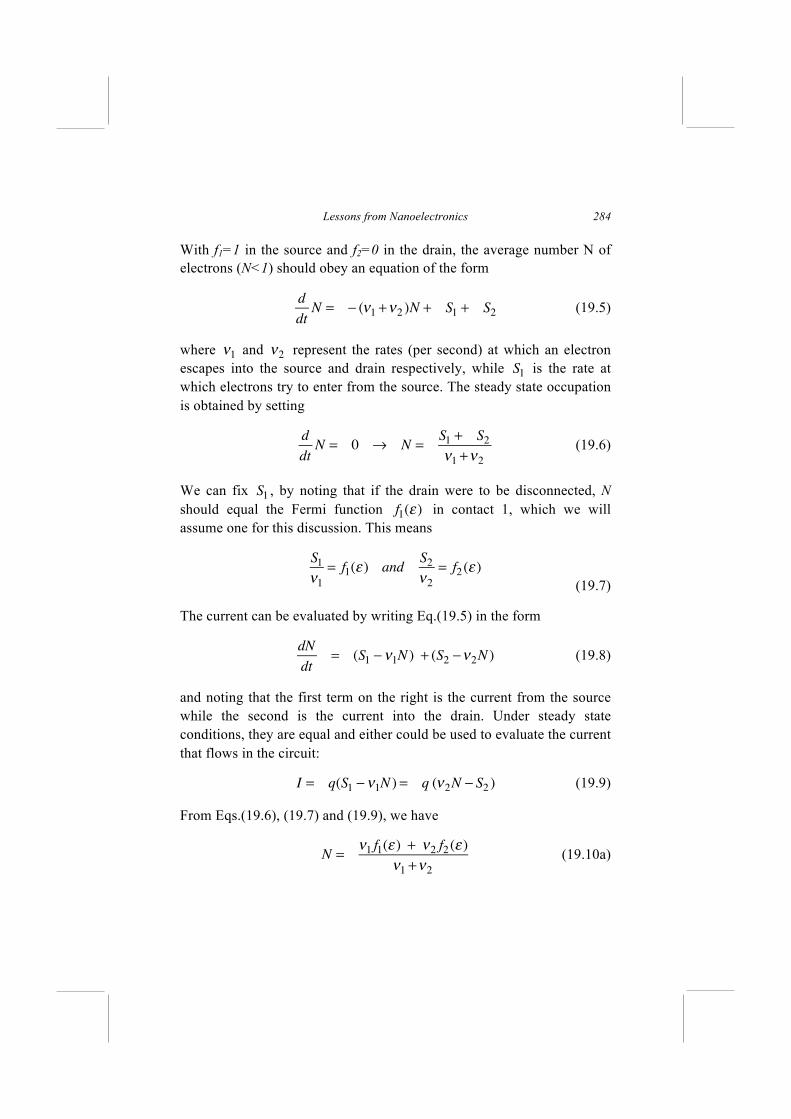
19.1.One-level resistor
To get a feeling for the NEGF method, it is instructive to look at a particularly simple conductor having just one level and described by a 1x1 [H] matrix that is essentially a number: . Starting directly from the Schrödinger equation we will see how we can introduce contacts into this problem. This will help set the stage for Section 19.3 when we consider arbitrary channels described by (NxN) matrices instead of the simple one-level channel described by (1x1) “matrices.”
19.1.1. Semiclassical treatment
It is useful to first go through a semiclassical treatment as an intuitive guide to the quantum treatment. Physically we have a level connected to two contacts, with two different occupancy factors
f1(ε ) and f2(ε )
Let us assume the occupation factor to be one for the source and zero for the drain, so that it is only the source that is continually trying to fill up the level while the drain is trying to empty it. We will calculate the resulting current and then multiply it by
f1(ε ) − f2(ε )
to account for the fact that there is injection from both sides and the net current is the difference.
Fig.19.2. Filling and emptying a level: Semiclassical picture
[H ] = ε
Lessons from Nanoelectronics
284
With f1=1 in the source and f2=0 in the drain, the average number N of electrons (N<1) should obey an equation of the form
d
dtN = − (ν1 +ν2 )N + S1 + S2 (19.5)
where ν1 and ν2 represent the rates (per second) at which an electron escapes into the source and drain respectively, while S1 is the rate at which electrons try to enter from the source. The steady state occupation is obtained by setting
d
dtN = 0 → N =
S1 + S2
ν1 +ν2
(19.6)
We can fix S1 , by noting that if the drain were to be disconnected, N should equal the Fermi function f1(ε ) in contact 1, which we will assume one for this discussion. This means
S1
ν1
= f1(ε ) andS2
ν2
= f2(ε )
(19.7)
The current can be evaluated by writing Eq.(19.5) in the form
dN
dt= (S1 −ν1N ) + (S2 −ν2N ) (19.8)
and noting that the first term on the right is the current from the source while the second is the current into the drain. Under steady state conditions, they are equal and either could be used to evaluate the current that flows in the circuit:
I = q(S1 −ν1N ) = q (ν2N − S2 ) (19.9)
From Eqs.(19.6), (19.7) and (19.9), we have
N =ν1 f1(ε ) + ν2 f2(ε )
ν1 +ν2
(19.10a)
NEGF Method
285
and I = q
ν1ν2
ν1 +ν2f1(ε ) − f2(ε )( ) (19.10b)
19.1.2. Quantum treatment
Let us now work out the same problem using a quantum formalism based on the Schrödinger equation. In the last Chapter we introduced the matrix version of the time-independent Schrödinger equation
E{ψ } = [H ]{ψ ]
which can be obtained from the more general time-dependent equation
i∂
∂t{ ψ (t)} = [H ]{ ψ (t)] (19.11a)
by assuming { ψ (t)} = {ψ } e−iEt / (19.11b)
For problems involving steady-state current flow, the time-independent version is usually adequate, but sometimes it is useful to go back to the time-dependent version because it helps us interpret certain quantities like the self-energy functions as we will see shortly.
In the quantum formalism the squared magnitude of the electronic wavefunction
ψ (t) tells us the probability of finding an electron
occupying the level and hence can be identified with the average number of electrons N ( < 1). For a single isolated level with [H] = ε , the time evolution of the wavefunction is described by
id
dtψ = ε ψ
which with a little algebra leads to
d
dtψ ψ *( ) = 0
Lessons from Nanoelectronics
286
showing that for an isolated level, the number of electrons ψ ψ * does
not change with time. Our interest, however, is not in isolated systems, but in channels connected to two contacts. Unfortunately the standard quantum mechanics literature does not provide much guidance in the matter, but we can do something relatively simple using the rate equation in Eq.(19.4) as a guide. We introduce contacts into the Schrödinger equation by modifying it to read
id
dtψ = ε − i
γ 1 + γ 22
⎛⎝⎜
⎞⎠⎟ψ (19.12a)
so that the resulting equation for
d
dtψ ψ * = −
γ 1 + γ 2
⎛⎝⎜
⎞⎠⎟ψ ψ * (19.12b)
looks just like Eq.(19.5) except for the source term S1 which we will discuss shortly.
We can make Eq.(19.12b) match Eq.(19.5) if we choose
γ 1 = ν1 (19.13a)
γ 2 = ν2 (19.13b)
We can now go back to the time-independent version of Eq.(19.12a):
Eψ = ε − iγ 1 + γ 22
⎛⎝⎜
⎞⎠⎟ψ (19.14)
obtained by assuming a single energy solution:
ψ (t) = ψ (E) e−iEt /
NEGF Method
287
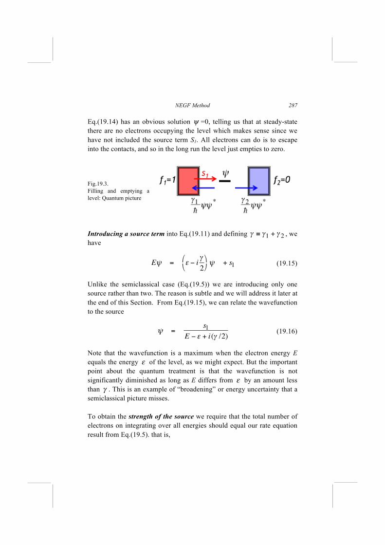
Eq.(19.14) has an obvious solution ψ =0, telling us that at steady-state there are no electrons occupying the level which makes sense since we have not included the source term S1. All electrons can do is to escape into the contacts, and so in the long run the level just empties to zero. Fig.19.3. Filling and emptying a level: Quantum picture Introducing a source term into Eq.(19.11) and defining , we have
(19.15)
Unlike the semiclassical case (Eq.(19.5)) we are introducing only one source rather than two. The reason is subtle and we will address it later at the end of this Section. From Eq.(19.15), we can relate the wavefunction to the source
(19.16)
Note that the wavefunction is a maximum when the electron energy E equals the energy ε of the level, as we might expect. But the important point about the quantum treatment is that the wavefunction is not significantly diminished as long as E differs from ε by an amount less than γ . This is an example of “broadening” or energy uncertainty that a semiclassical picture misses. To obtain the strength of the source we require that the total number of electrons on integrating over all energies should equal our rate equation result from Eq.(19.5). that is,
€
γ ≡ γ1 + γ 2
€
Eψ = ε − iγ
2
ψ + s1
€
ψ =s1
E − ε + i(γ /2)
Lessons from Nanoelectronics
288
dEψψ *− ∞
+ ∞
∫ =ν1
ν1 +ν2=
γ 1γ 1 + γ 2
(19.17)
where we have made use of Eq.(19.13). We now use Eqs.(19.16), (19.17) to evaluate the right hand side in terms of the source
dEψψ *− ∞
+ ∞
∫ = dEs1s1 *
(E − ε )2 +γ2
⎛⎝⎜
⎞⎠⎟2
− ∞
+ ∞
∫ =2π s1s1 *
γ (19.18)
where we have made use of a standard integral
dEγ
(E − ε )2 +γ2
⎛⎝⎜
⎞⎠⎟2
− ∞
+ ∞
∫ = 2π
(19.19)
From Eqs.(19.17) and (19.18) we obtain, noting that ,
2π s1s1* = γ 1 (19.20)
The strength of the source is thus proportional to the escape rate which seems reasonable: if the contact is well coupled to the channel and electrons can escape easily, they should also be able to come in easily. Just as in the semiclassical case (Eq.(19.9)) we obtain the current by looking at the rate of change of N from Eq.(19.12b)
d
dtψ ψ * = (Inflow from 1) −
γ 1
ψ ψ * −
γ 2
ψ ψ *
where we have added a term “Inflow from 1” as a reminder that Eq.(19.12a) does not include a source term. Both left and right hand sides of this equation are zero for the steady-state solutions we are considering. But just like the semiclassical case, we can identify the current as either the first two terms or the last term on the right:
NEGF Method
289
I
q= (Inflow from 1) −
γ 1
ψ ψ * =
γ 2
ψ ψ *
Using the second form and integrating over energy we can write
I = q dEγ 2
− ∞
+ ∞
∫ ψψ * (19.21)
so that making use of Eqs.(19.16) and (19.20), we have
I =q
γ 1γ 22π
dE1
(E − ε )2 + γ / 2( )2
− ∞
+ ∞
∫ (19.22)
which can be compared to the semiclassical result from Eq.(19.10) with f1=1, f2=0 (note: γ = γ 1 + γ 2 )
I =q
h
γ 1γ 2
γ 1 + γ 2
19.1.3. Quantum broadening
Note that Eq.(19.22) involves an integration over energy, as if the quantum treatment has turned the single sharp level into a continuous distribution of energies described by a density of states D(E):
(19.23)
Quantum mechanically the process of coupling inevitably spreads a single discrete level into a state that is distributed in energy, but integrated over all energy still equals one (see Eq.(19.15)). One could call it a consequence of the uncertainty relation
D =γ / 2π
(E − ε )2 + (γ / 2)2
€
γ t ≥ h
Lessons from Nanoelectronics
290
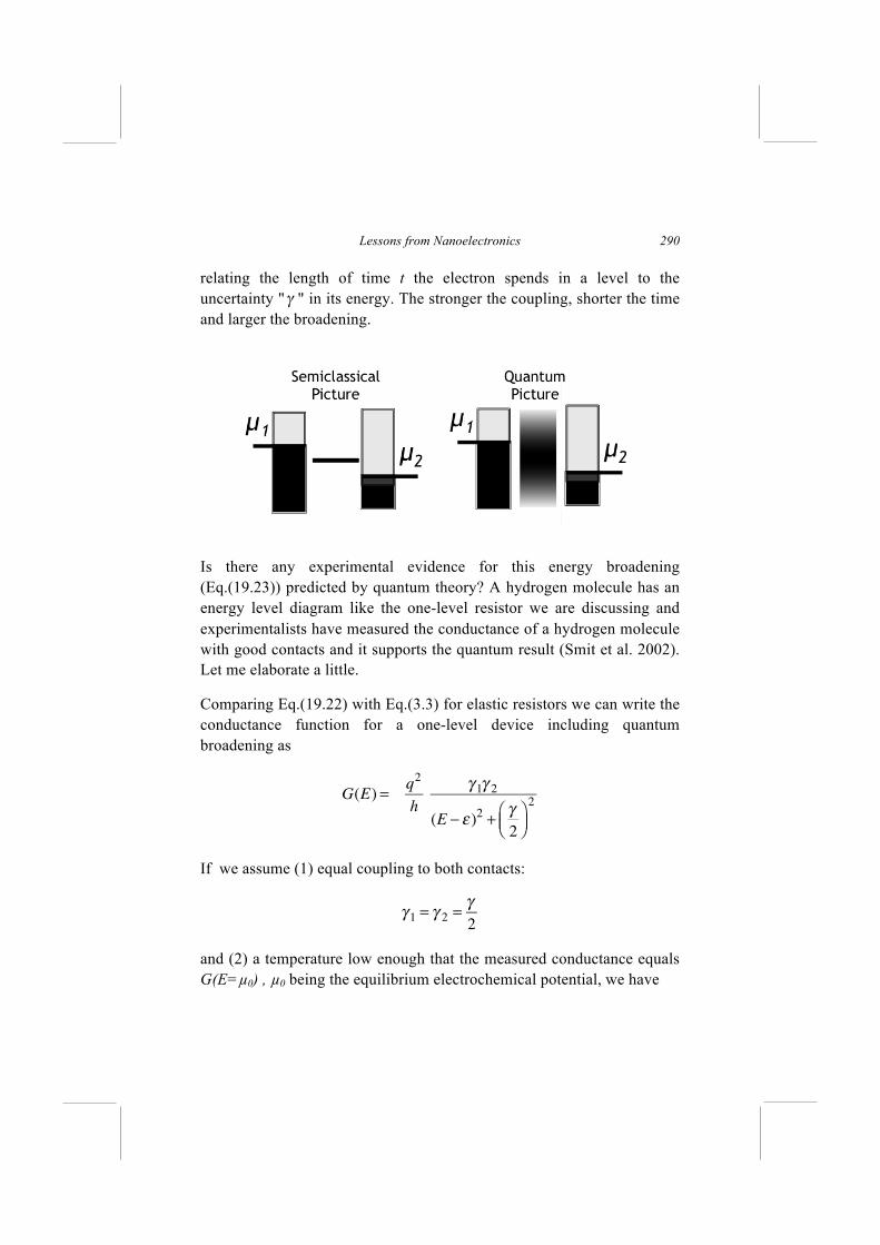
relating the length of time t the electron spends in a level to the uncertainty " " in its energy. The stronger the coupling, shorter the time and larger the broadening.
Is there any experimental evidence for this energy broadening (Eq.(19.23)) predicted by quantum theory? A hydrogen molecule has an energy level diagram like the one-level resistor we are discussing and experimentalists have measured the conductance of a hydrogen molecule with good contacts and it supports the quantum result (Smit et al. 2002). Let me elaborate a little.
Comparing Eq.(19.22) with Eq.(3.3) for elastic resistors we can write the conductance function for a one-level device including quantum broadening as
G(E) =q2
h
γ 1γ 2
(E − ε )2 +γ2
⎛⎝⎜
⎞⎠⎟2
If we assume (1) equal coupling to both contacts:
γ 1 = γ 2 =γ
2
and (2) a temperature low enough that the measured conductance equals G(E=µ0) , µ0 being the equilibrium electrochemical potential, we have
€
γ
NEGF Method
291
G ≈G(E = µ0 ) =q2
h
γ / 2( )2
(µ0 − ε )2+ γ / 2( )2
So the quantum theory of the one-level resistor says that the measured conductance should show a maximum value equal to the quantum of conductance q2/h when µ0 is located sufficiently close to ε . The experimentally measured conductance is equal to 2q2/h, the extra factor of 2 being due to spin degeneracy, since levels come in pairs and what we have is really a two-level rather than a one-level resistor.
19.1.4. Do Multiple Sources Interfere?
In our quantum treatment we considered a problem with electrons injected only from the source (f1 = 1) with the drain empty (f2 = 0) (Eq.(19.15)), unlike the semiclassical case where we started with both sources S1 and S2 (Eq.(19.5)). This is not just a matter of convenience. If instead of Eq.(19.15) we start from
Eψ = ε − iγ2
⎛⎝⎜
⎞⎠⎟ψ + s1 + s2
we obtain ψ =s1 + s2
E − ε + iγ
2
so that
ψψ * =1
E − ε( )2+
γ2
⎛⎝⎜
⎞⎠⎟2( s1s1 *+s2s2 * + s1s2 *+s2s1 *
InterferenceTerms
)
which has two extra interference terms that are never observed experimentally because the electrons injected from separate contacts have uncorrelated phases that change randomly in time and average to zero.
Lessons from Nanoelectronics
292
The first two terms on the other hand add up since they are positive numbers. It is like adding up the light from two light bulbs: we add their powers not their electric fields. Laser sources on the other hand can be coherent so that we actually add electric fields and the interference terms can be seen experimentally. Electron sources from superconducting contacts too can be coherent leading to Josephson currents that depend on interference. But that is a different matter. Our point here is simply that normal contacts like the ones we are discussing are incoherent and it is necessary to take that into account in our models. The moral of the story is that we cannot just insert multiple sources into the Schrödinger equation. We should insert one source at a time, calculate bilinear quantities (things that depend on the product of wavefunctions) like electron density and current and add up the contributions from different sources. Next we will describe the non-equilibrium Green function (NEGF) method that allows us to implement this procedure in a systematic way and also to include incoherent processes.
19.2. Quantum transport through multiple levels
We have seen how we can treat quantum transport through a one-level resistor with a time-independent Schrödinger equation modified to include the connection to contacts and a source term:
Eψ = ε − iγ2
⎛⎝⎜
⎞⎠⎟ψ + s
How do we extend this method to a more general channel described by an NxN Hamiltonian matrix [H] whose eigenvalues give the N energy levels?
For an N-level channel , the wavefunction {ψ } and source term {s1} are Nx1 column vectors and the modified Schrödinger equation looks like
E {ψ } = [H + Σ1 + Σ2 ] {ψ } + {s1} (19.24)
NEGF Method
293
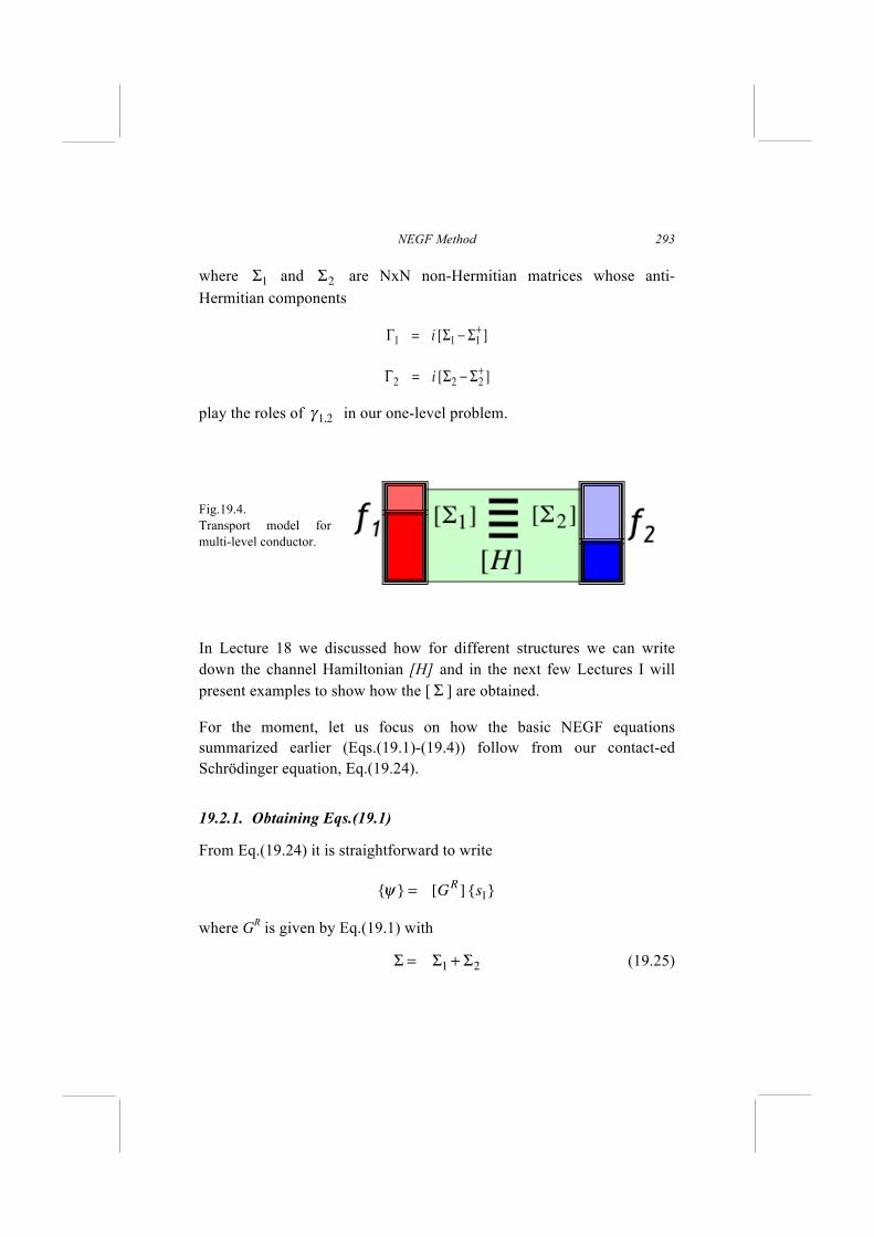
where Σ1 and Σ2 are NxN non-Hermitian matrices whose anti-Hermitian components
Γ1 = i [Σ1 − Σ1+]
Γ2 = i [Σ2 − Σ2+]
play the roles of γ 1,2 in our one-level problem.
Fig.19.4. Transport model for multi-level conductor.
In Lecture 18 we discussed how for different structures we can write down the channel Hamiltonian [H] and in the next few Lectures I will present examples to show how the [ Σ ] are obtained.
For the moment, let us focus on how the basic NEGF equations summarized earlier (Eqs.(19.1)-(19.4)) follow from our contact-ed Schrödinger equation, Eq.(19.24).
19.2.1. Obtaining Eqs.(19.1)
From Eq.(19.24) it is straightforward to write
{ψ } = [GR] {s1}
where GR is given by Eq.(19.1) with
Σ = Σ1 + Σ2 (19.25)
Lessons from Nanoelectronics
294
19.2.2. Obtaining Eqs.(19.2)
The matrix electron density, Gn, defined as
Gn→ 2π {ψ }{ψ }+ = 2π [GR
] {s1}{s1}+[G
A]
where the superscript "+" stands for conjugate transpose, and GA stands for the conjugate transpose of GR. For the one-level problem 2π s1s1* = γ 1 (see Eq.(19.20)): the corresponding matrix relation is
2π {s1}{s1}+= [Γ1]
so that Gn= [G
R] [Γ1] [G
A]
This is for a single source term. For multiple sources, the electron density matrices, unlike the wavefunctions, can all be added up with the appropriate Fermi function weighting to give Eq.(19.2),
Gn= [G
R] [Σ
in] [G
A] (same as 19.2)
with Σin representing an incoherent sum of all the independent sources:
[Σin] = [Γ1] f1(E) + [Γ2 ] f2(E) (19.26)
19.2.3. Obtaining Eq,(19.3)
Eq.(19.2) gives us the electron density matrix Gn, in terms of the Fermi functions f1 and f2 in the two contacts. But if both f1 and f2 are equal to one then all states are occupied, so that the matrix electron density becomes equal to the matrix density of states, called the spectral function matrix [A]. Setting f1 = 1 and f2 = 1, in Eq.(19.2) we have
[A] = [GR] [Γ] [G
A] (19.27)
NEGF Method
295
since Γ = Γ1 + Γ2 . This gives us part of Eq.(19.3). The rest of Eq.(19.3) can be obtained from Eq.(19.1) using straightforward algebra as follows:
[GR]−1
= EI − H − Σ (19.28a)
Taking conjugate transpose of both sides
[GR]−1⎡
⎣⎤⎦
+
= [GR]+⎡
⎣⎤⎦
−1= EI − H − Σ+ (19.28b)
Subtracting Eq.(19.28b) from (19.28a) (note that GA stands for [GR]+) and making use of Eq.(19.3b)
[GR]−1
− [GA]−1
= i [Γ] (19.28c)
Mutiplying with [GR] from the left and [GA] from the right we have
i [GR]− [GA
]⎡⎣
⎤⎦ = G
R ΓGA
thus giving us another piece of Eq.(19.3). The final piece is obtained by multiplying Eq.(19.28c) with [GA] from the left and [GR] from the right.
19.2.4. Obtaining Eq,(19.4): The Current Equation
Like the semiclassical treatment and the one-level quantum treatment, the current expression is obtained by considering the time variation of the number of electrons N. Starting from
id
dt{ψ } = [H + Σ] {ψ } + {s}
and its conjugate transpose (noting that H is a Hermitian matrix)
− id
dt{ψ }+ = {ψ }+ [H + Σ+
] + {s}+
Lessons from Nanoelectronics
296
we can write
id
dt{ψ }{ψ }+ = i
d
dt{ψ }⎛
⎝⎜⎞⎠⎟{ψ }+ + {ψ } i
d
dt{ψ }+⎛
⎝⎜⎞⎠⎟
= [H + Σ] {ψ } + {s}( ){ψ }+ − {ψ } {ψ }+ [H + Σ+] + {s}
+( )
= [(H + Σ)ψψ + −ψψ +(H + Σ+
)] + [ss+GA −GR
ss+]
where we have made use of the relations
{ψ } = [GR] {s} and {ψ }+ = {s}
+[G
A]
Since the trace of [ψψ + ] represents the number of electrons, we could define its time derivative as a matrix current operator whose trace gives us the current. Noting further that
2π {ψ }{ψ }+ = [Gn] and 2π {s}{s}+ = [Γ]
we can write
Iop
=[HG
n−G
nH ] + [ΣG
n−G
nΣ+] + [Σ
inGA−G
RΣin]
i2π (19.29)
This current operator provides a good starting point for discussing more subtle quantities like spin currents, but for the moment we will focus on ordinary currents requiring just the trace of this operator which tells us the time rate of change of the number of electrons N in the channel
d N
d t=
− i
hTrace [ΣG
n−G
nΣ+] + [Σ
inGA−G
RΣin]( )
noting that Trace [AB] = Trace [BA]. Making use of Eq.(19.3b)
dN
dt=
1
hTrace ΣinA − ΓGn⎡
⎣⎤⎦
NEGF Method
297
Now comes a tricky argument. Both the left and the right hand sides of Eq.(19.29) are zero, since we are discussing steady state transport with no time variation. The reason we are spending all this time discussing something that is zero is that the terms on the left can be separated into two parts, one associated with contact 1 and one with contact 2. They tell us the currents at contacts 1 and 2 respectively and the fact that they add up to zero is simply a reassuring statement of Kirchhoff’s law for steady-state currents in circuits.
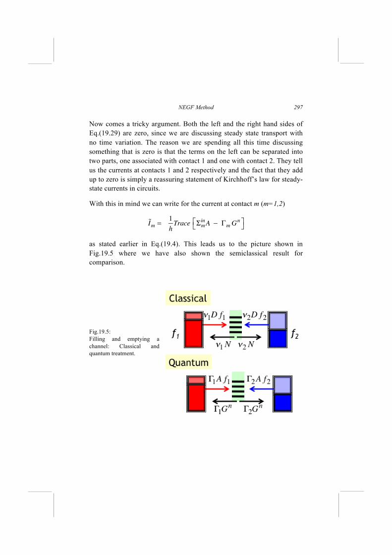
With this in mind we can write for the current at contact m (m=1,2)
Im =1
hTrace Σm
inA − ΓmG
n⎡⎣
⎤⎦
as stated earlier in Eq.(19.4). This leads us to the picture shown in Fig.19.5 where we have also shown the semiclassical result for comparison.
Fig.19.5: Filling and emptying a channel: Classical and quantum treatment.
Lessons from Nanoelectronics
298
19.3. Conductance Functions for Coherent Transport
Finally we note that using Eqs.(19.2)-(19.3) we can write the current from Eq.(19.4) a little differently
I (E) =q
hTrace[Γ1G
RΓ2G
A] f1(E)− f2(E)( )
which is very useful for it suggests a quantum expression for the conductance function G(E) that we introduced in Lecture 3 for all elastic resistors:
G(E) =q2
hTrace Γ1G
RΓ2GA⎡
⎣⎤⎦ (19.30)
More generally with multiterminal conductors we could introduce a self-energy function for each contact and show that
Im =q
hr
∑ Tmn fm (E)− fn (E)( ) (19.31)
with Tmn ≡ Trace ΓmGRΓnG
A⎡⎣
⎤⎦ (19.32)
For low bias we can use our usual Taylor series expansion from Eq.(2.8) to translate the Fermi functions into electrochemical potentials so that Eq.(19.31) looks just like the Buttiker equation (Eq.(12.3)) with the conductance function given
Gm, n (E) ≡q2
hTrace ΓmG
R ΓnGA⎡
⎣⎤⎦ (19.33)
which is energy-averaged in the usual way for elastic resistors (see Eq.(3.1)).
Gm, n = dE −∂ f0∂E
⎛⎝⎜
⎞⎠⎟Gm,n (E)
−∞
+∞
∫
NEGF Method
299
19.4. Elastic Dephasing
So far we have focused on the physical contacts described by [ Σ1,2 ] and
the model as it stands describes coherent quantum transport where electrons travel coherently from source to drain in some static structure described by the Hamiltonian [H] without any interactions along the channel described by [ Σ0 ] (Fig.19.1). In order to include [ Σ0 ], however, no change is needed as far as Eqs.(19.1) through (19.4) is concerned. It is just that an additional term appears in the definition of Σ
, Σin :
Σ = Σ1 + Σ2 + Σ0
Γ = Γ1 + Γ2 + Γ0
[Σin] = [Γ1] f1(E) + [Γ2 ] f2(E) + [Σ0
in] (19.34)
What does [ Σ0 ] represent physically? From the point of view of the electron a solid does not look like a static medium described by [H], but like a rather turbulent medium with a random potential UR that fluctuates on a picosecond time scale. Even at fairly low temperatures when phonons have been frozen out, an individual electron continues to see a fluctuating potential due to all the other electrons, whose average is modeled by the scf potential we discussed in Section 18.2. These fluctuations do not cause any overall loss of momentum from the system of electrons, since any loss from one electron is picked up by another. However, they do cause fluctuations in the phase leading to fluctuations in the current. What typical current measurements tell us is an average flow over nanoseconds if not microseconds or milliseconds. This averaging effect needs to be modeled if we wish to relate to experiments.
Lessons from Nanoelectronics
300
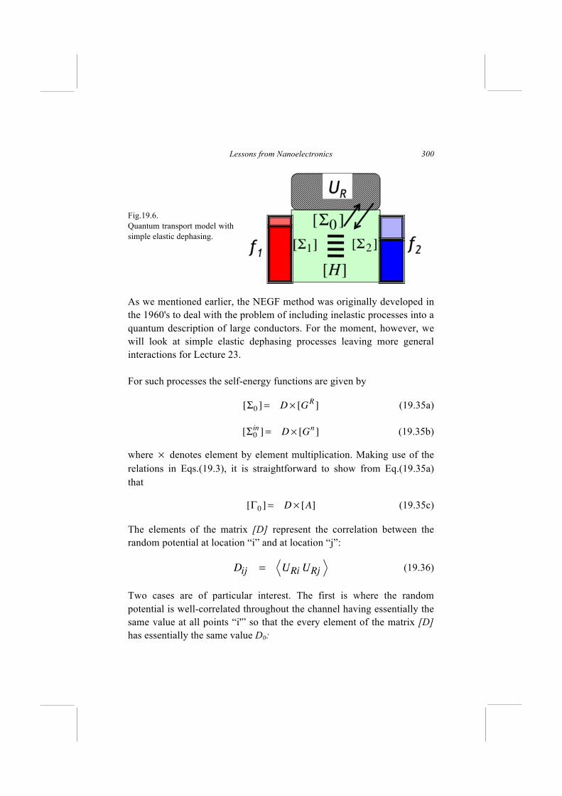
Fig.19.6. Quantum transport model with simple elastic dephasing. As we mentioned earlier, the NEGF method was originally developed in the 1960's to deal with the problem of including inelastic processes into a quantum description of large conductors. For the moment, however, we will look at simple elastic dephasing processes leaving more general interactions for Lecture 23. For such processes the self-energy functions are given by
[Σ0 ] = D × [GR] (19.35a)
[Σ0in] = D × [G
n] (19.35b)
where × denotes element by element multiplication. Making use of the relations in Eqs.(19.3), it is straightforward to show from Eq.(19.35a) that
[Γ0 ] = D × [A] (19.35c)
The elements of the matrix [D] represent the correlation between the random potential at location “i” and at location “j”:
(19.36)
Two cases are of particular interest. The first is where the random potential is well-correlated throughout the channel having essentially the same value at all points “i'” so that the every element of the matrix [D] has essentially the same value D0:
Dij = URi URj
NEGF Method
301
Model A: Dij = D0 (19.37)
The other case is where the random potential has zero correlation from one spatial point i to another j , so that
Model B:Dij = D0 , i = j and = 0 , i ≠ j (19.38)
Real processes are usually somewhere between the two extremes represented by models A and B. To see where Eqs.(19.35) come from we go back to our contact-ed Schrödinger equation
E {ψ } = [H + Σ1 + Σ2 ] {ψ } + {s1}
and noting that a random potential UR should lead to an additional term that could be viewed as an additional source term
E {ψ } = [H + Σ1 + Σ2 ] {ψ } + UR{ψ } + {s1}
with a corresponding inscattering term given by
Σ0in= 2π URUR
*{ψ }{ψ }+ = D0G
n
corresponding to Model A (Eq.(19.37)) and a little more careful argument leads to the more general result in Eq.(19.36). That gives us Eq.(19.35b). How about Eq.(19.35a) and (19.35c) ?
The simplest way to justify Eq.(19.35c) is to note that together with Eq.(19.35b) (which we just obtained) it ensures that the current at terminal 0 from Eq.(19.4) equals zero:
I0 =q
hTrace[Σ0
inA − Γ0G
n]
=q
hTrace[G
nΓ0 − Γ0G
n] = 0
Lessons from Nanoelectronics
302
This is a required condition since terminal 0 is not a physical contact where electrons can actually exit or enter from.
Indeed a very popular method due to Büttiker introduces incoherent processes by including a fictitious probe (often called a Büttiker probe) whose electrochemical potential is adjusted to ensure that it draws zero current. In NEGF language this amounts to assuming
Σ0in= Γ0 fP
with the number fP is adjusted for zero current. This would be equivalent to the approach described here if the probe coupling Γ0 were chosen proportional to the spectral function [A] as required by Eq.(19.35c).
Note that our prescription in Eq.(19.35) requires a “self-consistent evaluation” since Σ , Σin depend on GR and Gn which in turn depend on
Σ , Σin respectively (see Eqs.(19.1), (19.2)).
Also, Model A (Eq.(19.37)) requires us to calculate the full Green’s function which can be numerically challenging for large devices described by large matrices. Model B makes the computation numerically much more tractable because one only needs to calculate the diagonal elements of the Green’s functions which can be done much faster using powerful algorithms. In these Lectures, however, we focus on conceptual issues using “toy” problems for which numerical issues are not the “show stoppers.” The important conceptual distinction between Models A and B is that the former destroys phase but not momentum, while the latter destroys momentum as well [Golizadeh-Mojarad et al. 2007]. The dephasing process can be viewed as extraction of the electron from a state described by [Gn] and reinjecting it in a state described by D × Gn. Model A is equivalent to multiplying [Gn] by a constant so that the electron is reinjected in exactly the same state that it was extracted in, causing no loss of momentum, while Model B throws away the off-
NEGF Method
303
diagonal elements and upon reinjection the electron is as likely to go on way or another. Hopefully this will get clearer in the next Lecture when we look at a concrete example. Another question that the reader might raise is whether instead of including elastic dephasing through a self-energy function [Σ0 ] we could include a potential UR in the Hamiltonian itself and then average over a number of random realizations of UR. The answer is that the two methods are not exactly equivalent though in some problems they could yield similar results. This too should be a little clearer in the next lecture when we look at a concrete example. For completeness, let me note that in the most general case Dijkl is a fourth order tensor and the version we are using (Eq.(19.35)) represents a special case for which Dijkl is non-zero only if i=k, j=l (see Appendix E).
Lessons from Nanoelectronics
304
Lecture 20
Can Two Offer Less Resistance than One?
20.1. Modeling 1D Conductors 20.2. Quantum Resistors in Series 20.3. Potential Drop Across Scatterer(s)
In the next three Lectures we will go through a few examples of increasing complexity which are interesting in their own right but have been chosen primarily as “do it yourself” problems that the reader can use to get familiar with the quantum transport model outlined in the last Lecture. The MATLAB codes are all included in Appendix F.
In this Lecture we will use 1D quantum transport models to study an interesting question regarding multiple scatterers or obstacles along a conductor. Are we justified in neglecting all interference effects among them and assuming that electrons diffuse like classical particles as we do in the semiclassical picture?
This was the question Anderson raised in his 1958 paper entitled "Absence of Diffusion in Certain Random Lattices" pointing out that diffusion could be slowed significantly and even suppressed completely due to quantum interference between scatterers. “Anderson localization” is a vast topic and we are only using some related issues here to show how the NEGF model provides a convenient conceptual framework for studying interesting physics.
For any problem we need to discuss how we write down the Hamiltonian [H] and the contact self-energy matrices [ Σ ]. Once we have these, the computational process is standard. The rest is about understanding and enjoying the physics.
Can Two Offer Less Resistance than One?
305
20.1. Modeling 1D Conductors
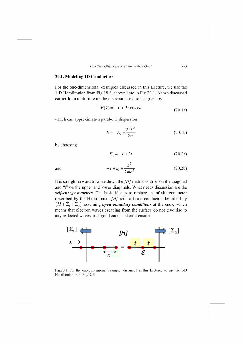
For the one-dimensional examples discussed in this Lecture, we use the 1-D Hamiltonian from Fig.18.6, shown here in Fig.20.1. As we discussed earlier for a uniform wire the dispersion relation is given by
(20.1a)
which can approximate a parabolic dispersion
E = Ec +2k2
2m (20.1b)
by choosing
Ec= ε + 2t (20.2a)
and
− t ≡ t0 ≡2
2ma2
(20.2b)
It is straightforward to write down the [H] matrix with ε on the diagonal and “t” on the upper and lower diagonals. What needs discussion are the self-energy matrices. The basic idea is to replace an infinite conductor described by the Hamiltonian [H] with a finite conductor described by
assuming open boundary conditions at the ends, which means that electron waves escaping from the surface do not give rise to any reflected waves, as a good contact should ensure.
Fig.20.1. For the one-dimensional examples discussed in this Lecture, we use the 1-D Hamiltonian from Fig.18.6.
E(k) = ε + 2t coska
[H + Σ1+ Σ
2]
Lessons from Nanoelectronics
306
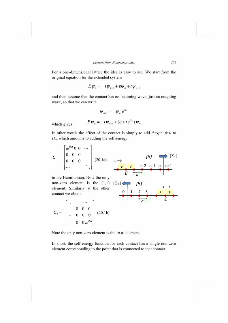
For a one-dimensional lattice the idea is easy to see. We start from the original equation for the extended system
and then assume that the contact has no incoming wave, just an outgoing wave, so that we can write
which gives
In other words the effect of the contact is simply to add t*exp(+ika) to Hnn which amounts to adding the self-energy
Σ1 =
teika0 0
0 0 0
0 0 0
⎡
⎣
⎢⎢⎢⎢⎢
⎤
⎦
⎥⎥⎥⎥⎥
(20.1a)
to the Hamiltonian. Note the only non-zero element is the (1,1) element. Similarly at the other contact we obtain
Σ2 =
0 0 0
0 0 0
0 0 teika
⎡
⎣
⎢⎢⎢⎢⎢
⎤
⎦
⎥⎥⎥⎥⎥
(20.1b)
Note the only non-zero element is the (n,n) element.
In short, the self-energy function for each contact has a single non-zero element corresponding to the point that is connected to that contact.
Eψn= tψ
n−1+ εψ
n+ tψ
n+1
ψn+1
= ψneika
Eψn= tψ
n−1+ (ε + t eika )ψ
n
Can Two Offer Less Resistance than One?
307
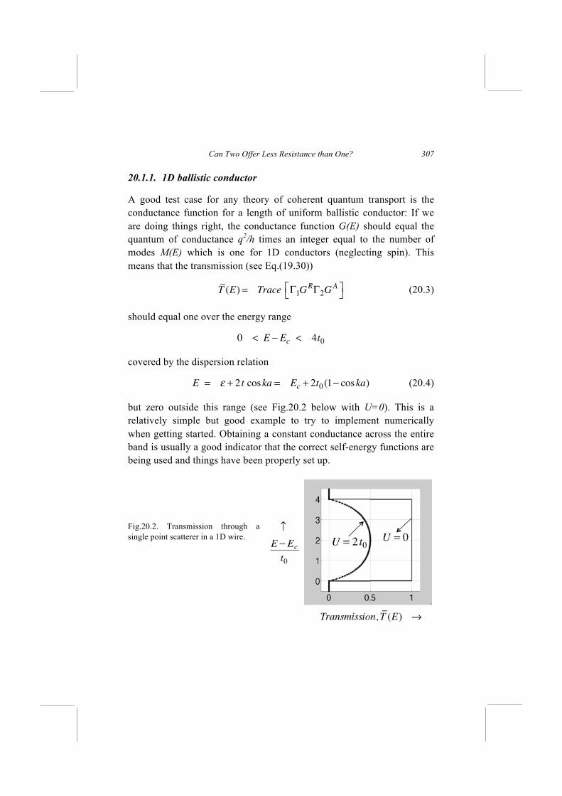
20.1.1. 1D ballistic conductor
A good test case for any theory of coherent quantum transport is the conductance function for a length of uniform ballistic conductor: If we are doing things right, the conductance function G(E) should equal the quantum of conductance q2/h times an integer equal to the number of modes M(E) which is one for 1D conductors (neglecting spin). This means that the transmission (see Eq.(19.30))
T (E) = Trace Γ1GRΓ2G
A⎡⎣
⎤⎦ (20.3)
should equal one over the energy range
0 < E − Ec< 4t0
covered by the dispersion relation
E = ε + 2 t coska = Ec + 2t0(1− coska) (20.4)
but zero outside this range (see Fig.20.2 below with U=0). This is a relatively simple but good example to try to implement numerically when getting started. Obtaining a constant conductance across the entire band is usually a good indicator that the correct self-energy functions are being used and things have been properly set up.
Fig.20.2. Transmission through a single point scatterer in a 1D wire.
Lessons from Nanoelectronics
308
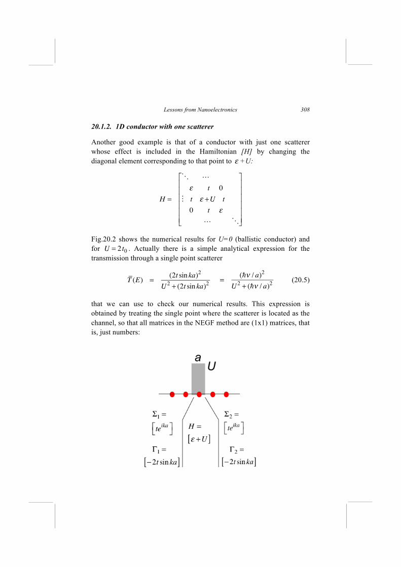
20.1.2. 1D conductor with one scatterer
Another good example is that of a conductor with just one scatterer whose effect is included in the Hamiltonian [H] by changing the diagonal element corresponding to that point to ε +U:
H =
ε t 0
t ε +U t
0 t ε
⎡
⎣
⎢⎢⎢⎢⎢⎢
⎤
⎦
⎥⎥⎥⎥⎥⎥
Fig.20.2 shows the numerical results for U=0 (ballistic conductor) and for U = 2 t0 . Actually there is a simple analytical expression for the transmission through a single point scatterer
T (E) =(2t sin ka)
2
U2+ (2t sin ka)
2
=(ν / a)
2
U2+ (ν / a)
2 (20.5)
that we can use to check our numerical results. This expression is obtained by treating the single point where the scatterer is located as the channel, so that all matrices in the NEGF method are (1x1) matrices, that is, just numbers:
Can Two Offer Less Resistance than One?
309
It is easy to see that the Green’s function is given by
GR(E) =
1
E − (ε +U )− 2t eika
=1
−U − i2t sin ka
making use of Eq.(20.2). Hence
Γ1GRΓ2G
A=
(2t sin ka)2
U2+ (2t sin ka)
2
giving us the stated result in Eq.(20.3). The second form is obtained by noting from Eq.(20.2) that
ν =dE
dk= − 2at sin ka
(20.6)
Once you are comfortable with the results in Fig.20.2 and are able to reproduce it, you should be ready to include various potentials into the Hamiltonian and reproduce the rest of the examples in this Lecture.
20.2. Quantum Resistors in Series
In Lecture 12 we argued that the resistance of a conductor with one scatterer with a transmission probability T can be divided into a scatterer resistance and an interface resistance (see Eqs.(12.1), (12.2))
R1 =h
q2M
1−TT
scatterer
+ 1
interface
⎛
⎝
⎜⎜⎜
⎞
⎠
⎟⎟⎟
What is the resistance if we have two scatterers each with transmission T?
Lessons from Nanoelectronics
310
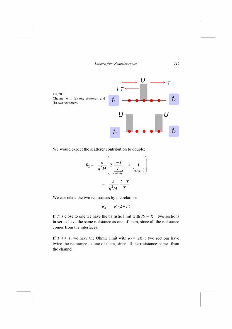
Fig.20.3. Channel with (a) one scatterer, and (b) two scatterers.
We would expect the scatterer contribution to double:
R2 =h
q2M
21−TT
scatterer
+ 1
interface
⎛
⎝
⎜⎜⎜
⎞
⎠
⎟⎟⎟
=h
q2M
2 −T
T
We can relate the two resistances by the relation:
R2 = R1 (2 −T )
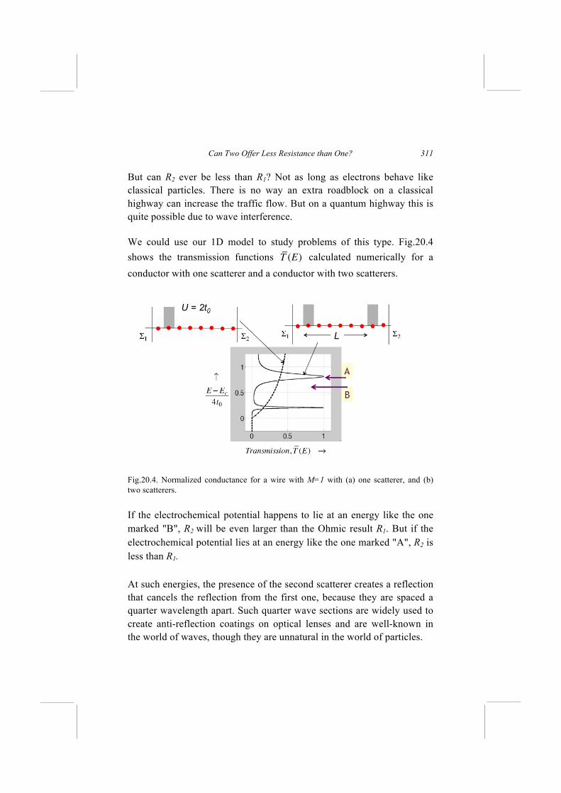
If T is close to one we have the ballistic limit with R2 = R1 : two sections in series have the same resistance as one of them, since all the resistance comes from the interfaces. If T << 1, we have the Ohmic limit with R2 = 2R1 : two sections have twice the resistance as one of them, since all the resistance comes from the channel.
Can Two Offer Less Resistance than One?
311
But can R2 ever be less than R1? Not as long as electrons behave like classical particles. There is no way an extra roadblock on a classical highway can increase the traffic flow. But on a quantum highway this is quite possible due to wave interference. We could use our 1D model to study problems of this type. Fig.20.4 shows the transmission functions T (E) calculated numerically for a conductor with one scatterer and a conductor with two scatterers.
Fig.20.4. Normalized conductance for a wire with M=1 with (a) one scatterer, and (b) two scatterers. If the electrochemical potential happens to lie at an energy like the one marked "B", R2 will be even larger than the Ohmic result R1. But if the electrochemical potential lies at an energy like the one marked "A", R2 is less than R1. At such energies, the presence of the second scatterer creates a reflection that cancels the reflection from the first one, because they are spaced a quarter wavelength apart. Such quarter wave sections are widely used to create anti-reflection coatings on optical lenses and are well-known in the world of waves, though they are unnatural in the world of particles.
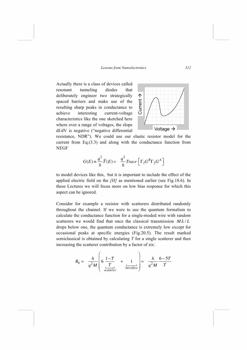
Lessons from Nanoelectronics
312
Actually there is a class of devices called resonant tunneling diodes that deliberately engineer two strategically spaced barriers and make use of the resulting sharp peaks in conductance to achieve interesting current-voltage characteristics like the one sketched here where over a range of voltages, the slope dI/dV is negative (“negative differential resistance, NDR”). We could use our elastic resistor model for the current from Eq.(3.3) and along with the conductance function from NEGF
G(E) ≡q2
hT (E) =
q2
hTrace Γ1G
RΓ2GA⎡
⎣⎤⎦
to model devices like this, but it is important to include the effect of the applied electric field on the [H] as mentioned earlier (see Fig.18.6). In these Lectures we will focus more on low bias response for which this aspect can be ignored. Consider for example a resistor with scatterers distributed randomly throughout the channel. If we were to use the quantum formalism to calculate the conductance function for a single-moded wire with random scatterers we would find that once the classical transmission Mλ / L drops below one, the quantum conductance is extremely low except for occasional peaks at specific energies (Fig.20.5). The result marked semiclassical is obtained by calculating T for a single scatterer and then increasing the scatterer contribution by a factor of six:
R6 =h
q2M
61−TT
scatterer
+ 1
interface
⎛
⎝
⎜⎜⎜
⎞
⎠
⎟⎟⎟=
h
q2M
6 − 5TT
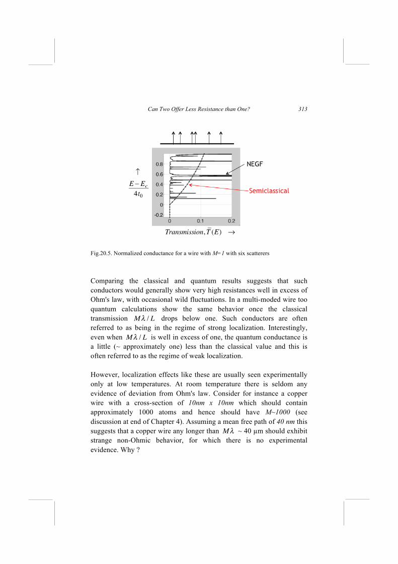
Can Two Offer Less Resistance than One?
313
Fig.20.5. Normalized conductance for a wire with M=1 with six scatterers Comparing the classical and quantum results suggests that such conductors would generally show very high resistances well in excess of Ohm's law, with occasional wild fluctuations. In a multi-moded wire too quantum calculations show the same behavior once the classical transmission Mλ / L drops below one. Such conductors are often referred to as being in the regime of strong localization. Interestingly, even when Mλ / L is well in excess of one, the quantum conductance is a little (~ approximately one) less than the classical value and this is often referred to as the regime of weak localization. However, localization effects like these are usually seen experimentally only at low temperatures. At room temperature there is seldom any evidence of deviation from Ohm's law. Consider for instance a copper wire with a cross-section of 10nm x 10nm which should contain approximately 1000 atoms and hence should have M~1000 (see discussion at end of Chapter 4). Assuming a mean free path of 40 nm this suggests that a copper wire any longer than Mλ ~ 40 µm should exhibit strange non-Ohmic behavior, for which there is no experimental evidence. Why ?
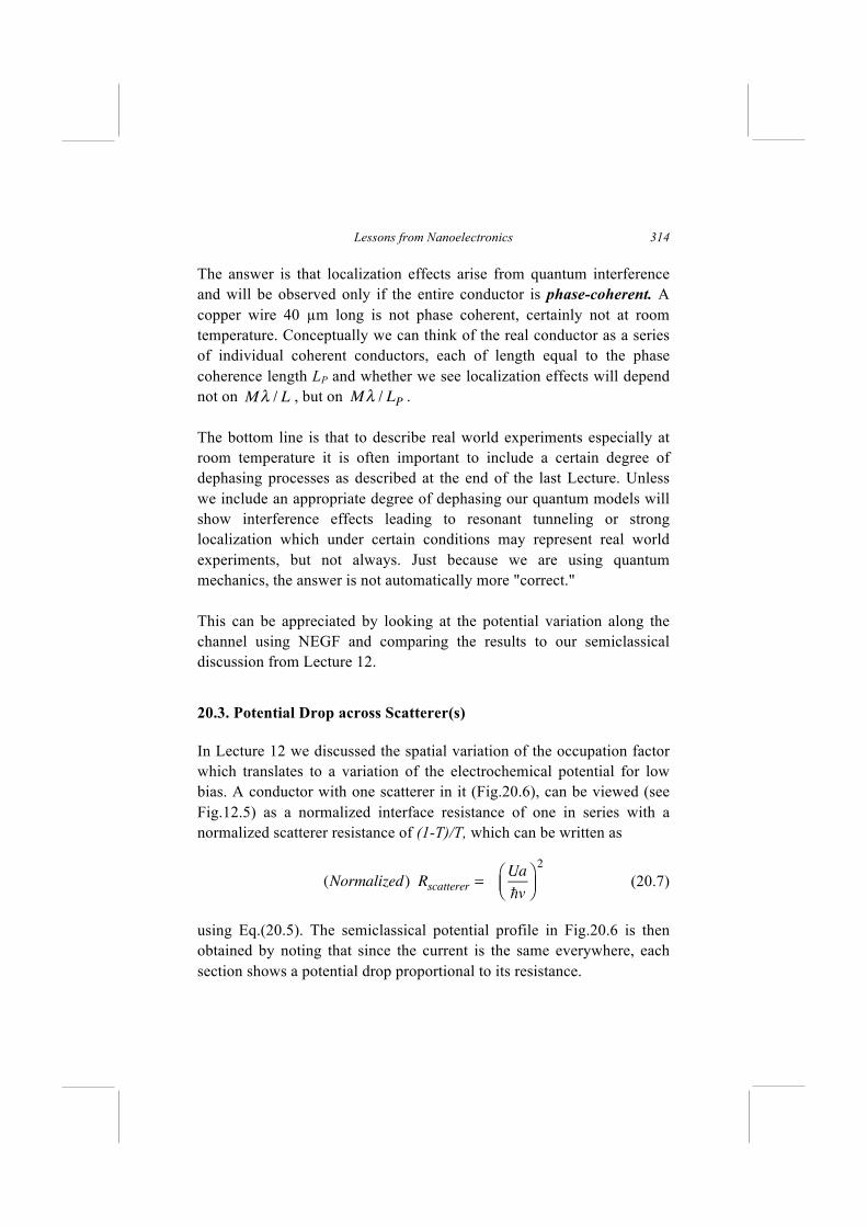
Lessons from Nanoelectronics
314
The answer is that localization effects arise from quantum interference and will be observed only if the entire conductor is phase-coherent. A copper wire 40 µm long is not phase coherent, certainly not at room temperature. Conceptually we can think of the real conductor as a series of individual coherent conductors, each of length equal to the phase coherence length LP and whether we see localization effects will depend not on Mλ / L , but on Mλ / L
P.
The bottom line is that to describe real world experiments especially at room temperature it is often important to include a certain degree of dephasing processes as described at the end of the last Lecture. Unless we include an appropriate degree of dephasing our quantum models will show interference effects leading to resonant tunneling or strong localization which under certain conditions may represent real world experiments, but not always. Just because we are using quantum mechanics, the answer is not automatically more "correct." This can be appreciated by looking at the potential variation along the channel using NEGF and comparing the results to our semiclassical discussion from Lecture 12.
20.3. Potential Drop across Scatterer(s)
In Lecture 12 we discussed the spatial variation of the occupation factor which translates to a variation of the electrochemical potential for low bias. A conductor with one scatterer in it (Fig.20.6), can be viewed (see Fig.12.5) as a normalized interface resistance of one in series with a normalized scatterer resistance of (1-T)/T, which can be written as
(Normalized) Rscatterer =Ua
v
⎛⎝⎜
⎞⎠⎟2
(20.7)
using Eq.(20.5). The semiclassical potential profile in Fig.20.6 is then obtained by noting that since the current is the same everywhere, each section shows a potential drop proportional to its resistance.
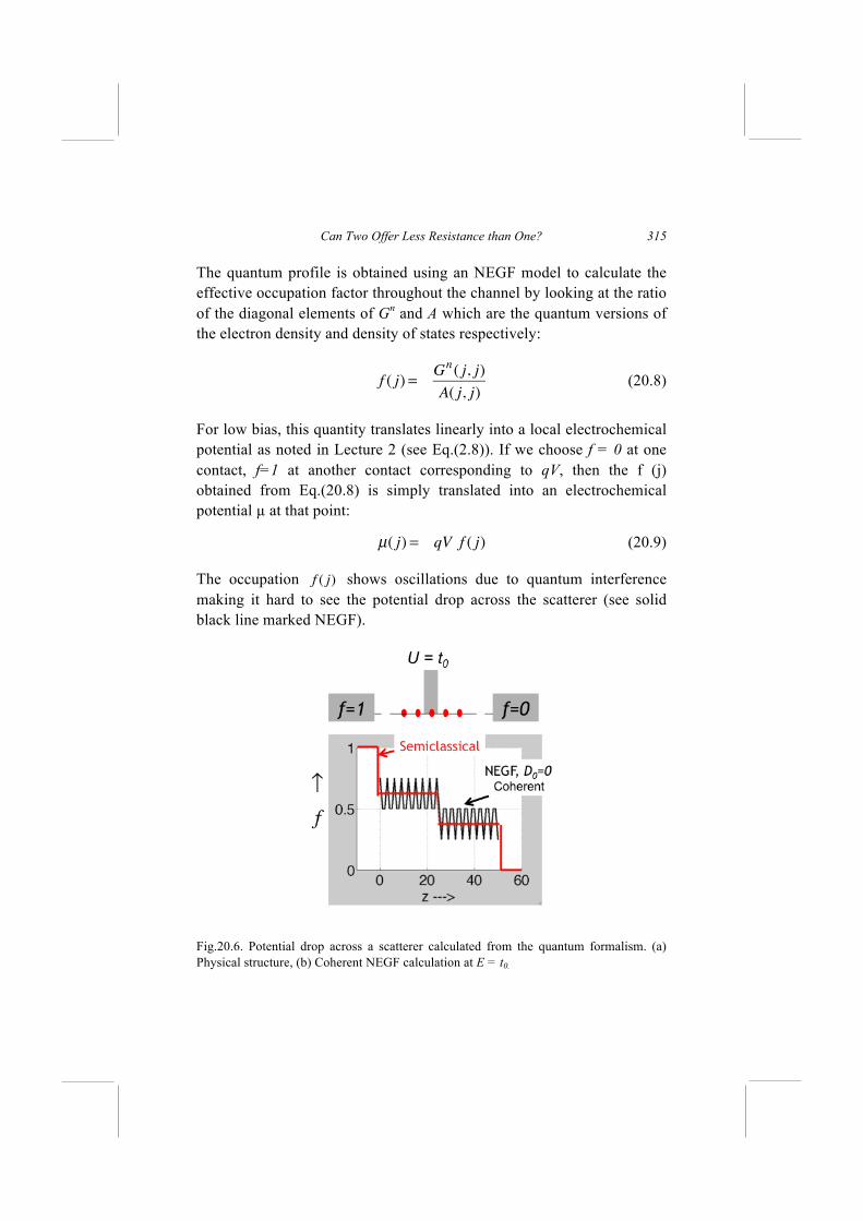
Can Two Offer Less Resistance than One?
315
The quantum profile is obtained using an NEGF model to calculate the effective occupation factor throughout the channel by looking at the ratio of the diagonal elements of Gn and A which are the quantum versions of the electron density and density of states respectively:
f ( j) =Gn( j, j)
A( j, j) (20.8)
For low bias, this quantity translates linearly into a local electrochemical potential as noted in Lecture 2 (see Eq.(2.8)). If we choose f = 0 at one contact, f=1 at another contact corresponding to qV, then the f (j) obtained from Eq.(20.8) is simply translated into an electrochemical potential µ at that point:
µ( j) = qV f ( j) (20.9)
The occupation f ( j) shows oscillations due to quantum interference making it hard to see the potential drop across the scatterer (see solid black line marked NEGF).
Fig.20.6. Potential drop across a scatterer calculated from the quantum formalism. (a) Physical structure, (b) Coherent NEGF calculation at E = t0.
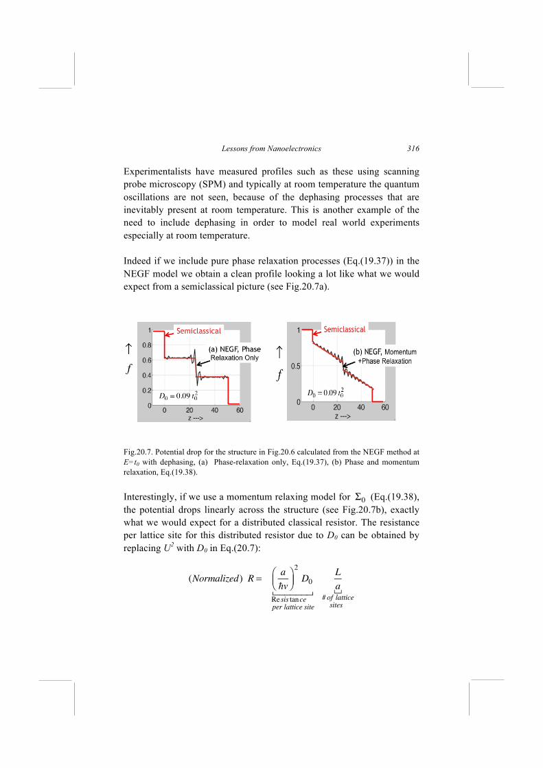
Lessons from Nanoelectronics
316
Experimentalists have measured profiles such as these using scanning probe microscopy (SPM) and typically at room temperature the quantum oscillations are not seen, because of the dephasing processes that are inevitably present at room temperature. This is another example of the need to include dephasing in order to model real world experiments especially at room temperature. Indeed if we include pure phase relaxation processes (Eq.(19.37)) in the NEGF model we obtain a clean profile looking a lot like what we would expect from a semiclassical picture (see Fig.20.7a).
Fig.20.7. Potential drop for the structure in Fig.20.6 calculated from the NEGF method at E=t0 with dephasing, (a) Phase-relaxation only, Eq.(19.37), (b) Phase and momentum relaxation, Eq.(19.38). Interestingly, if we use a momentum relaxing model for Σ0 (Eq.(19.38), the potential drops linearly across the structure (see Fig.20.7b), exactly what we would expect for a distributed classical resistor. The resistance per lattice site for this distributed resistor due to D0 can be obtained by replacing U2 with D0 in Eq.(20.7):
(Normalized) R =a
v
⎛⎝⎜
⎞⎠⎟2
D0
Re sis tanceper lattice site
L
a#of latticesites
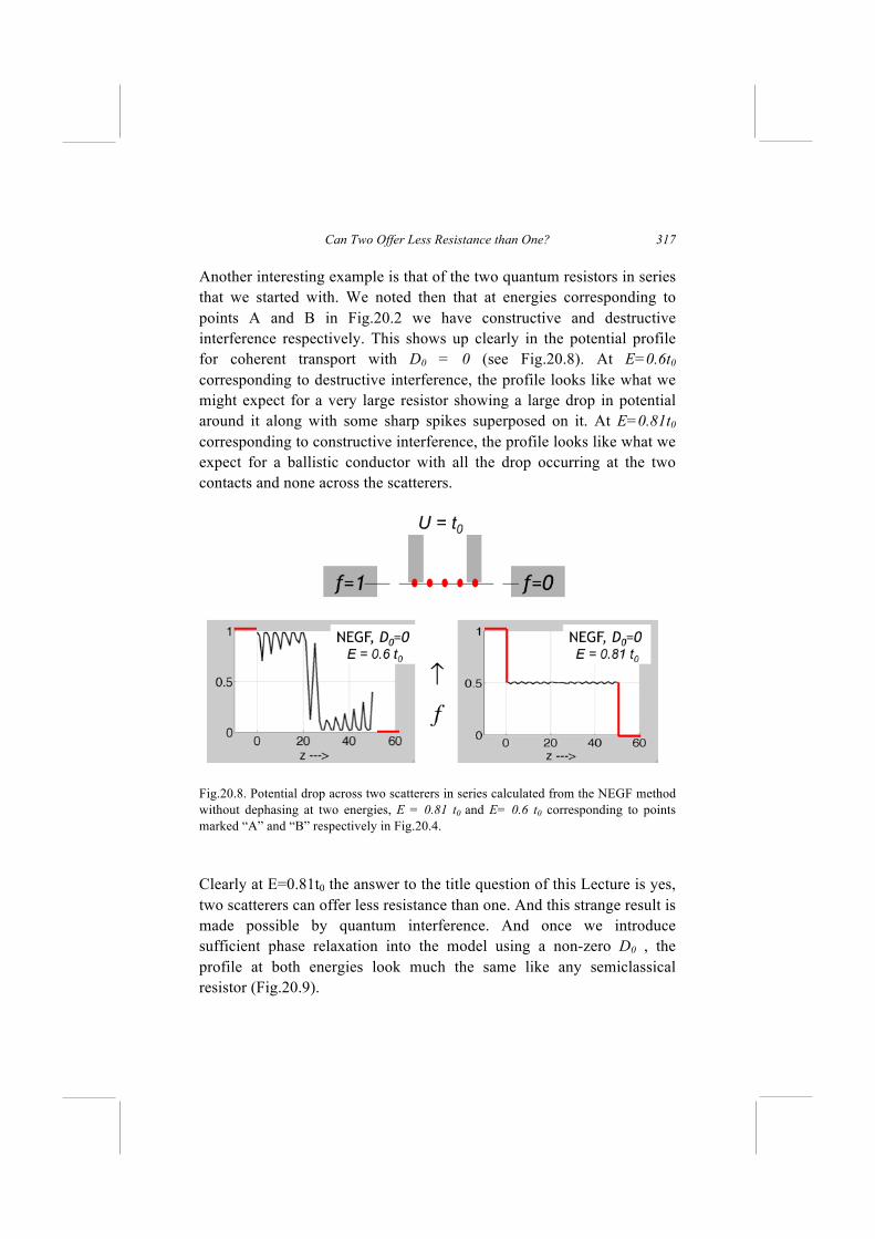
Can Two Offer Less Resistance than One?
317
Another interesting example is that of the two quantum resistors in series that we started with. We noted then that at energies corresponding to points A and B in Fig.20.2 we have constructive and destructive interference respectively. This shows up clearly in the potential profile for coherent transport with D0 = 0 (see Fig.20.8). At E=0.6t0 corresponding to destructive interference, the profile looks like what we might expect for a very large resistor showing a large drop in potential around it along with some sharp spikes superposed on it. At E=0.81t0 corresponding to constructive interference, the profile looks like what we expect for a ballistic conductor with all the drop occurring at the two contacts and none across the scatterers.
Fig.20.8. Potential drop across two scatterers in series calculated from the NEGF method without dephasing at two energies, E = 0.81 t0 and E= 0.6 t0 corresponding to points marked “A” and “B” respectively in Fig.20.4. Clearly at E=0.81t0 the answer to the title question of this Lecture is yes, two scatterers can offer less resistance than one. And this strange result is made possible by quantum interference. And once we introduce sufficient phase relaxation into the model using a non-zero D0 , the profile at both energies look much the same like any semiclassical resistor (Fig.20.9).
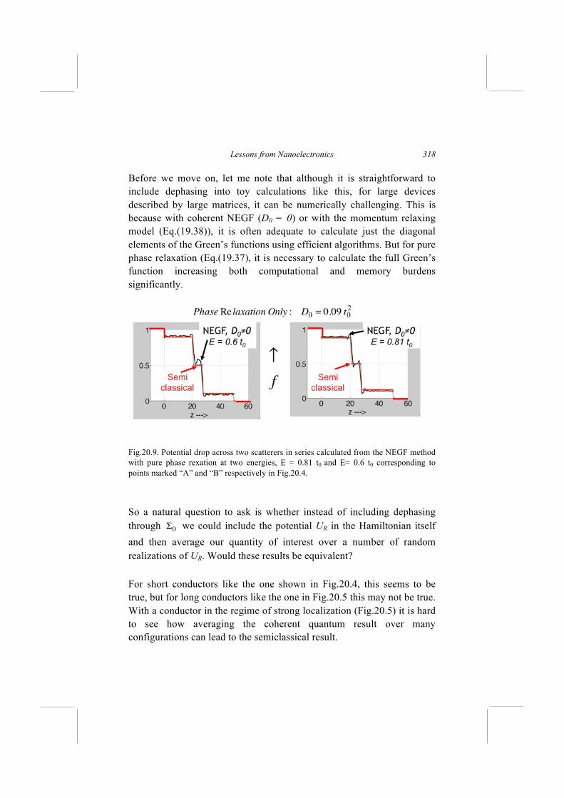
Lessons from Nanoelectronics
318
Before we move on, let me note that although it is straightforward to include dephasing into toy calculations like this, for large devices described by large matrices, it can be numerically challenging. This is because with coherent NEGF (D0 = 0) or with the momentum relaxing model (Eq.(19.38)), it is often adequate to calculate just the diagonal elements of the Green’s functions using efficient algorithms. But for pure phase relaxation (Eq.(19.37), it is necessary to calculate the full Green’s function increasing both computational and memory burdens significantly.
Fig.20.9. Potential drop across two scatterers in series calculated from the NEGF method with pure phase rexation at two energies, E = 0.81 t0 and E= 0.6 t0 corresponding to points marked “A” and “B” respectively in Fig.20.4. So a natural question to ask is whether instead of including dephasing through Σ0 we could include the potential UR in the Hamiltonian itself and then average our quantity of interest over a number of random realizations of UR. Would these results be equivalent? For short conductors like the one shown in Fig.20.4, this seems to be true, but for long conductors like the one in Fig.20.5 this may not be true. With a conductor in the regime of strong localization (Fig.20.5) it is hard to see how averaging the coherent quantum result over many configurations can lead to the semiclassical result.
Can Two Offer Less Resistance than One?
319
NEGF with dephasing does not just average over many configurations, it also averages over different sections of the same configuration and that is why it is able to capture the semiclassical result which often describes real world experiments at room temperature quite well. But could NEGF capture the localization effects observed at low temperatures through a proper choice of Σ0 ? We believe so, but it would involve going beyond the simple dephasing models (technically known as the self-consistent Born approximation) for evaluating Σ0 described in Section 19.4. One last comment before we move on. Note that our discussion of the potential profile has focused entirely on the electrochemical potential based on the transport equation, rather than the electrostatic potential obtained by self-consistently solving the Poisson equation with appropriate corrections if needed. The reason is that the electrostatic potential is approximately given by the electrochemical potential convolved with a screening function which is very sharp in metals, but more diffuse in semiconductors. It thus does not add much to our understanding of potential profiles, though a detailed consideration may be important in interpreting specific experiments. These issues were discussed at length in McLennan et al. (1991) referred in the last lecture and also in Chapter 2 of Datta (1995).
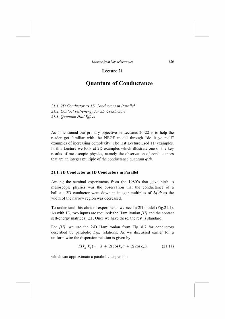
Lessons from Nanoelectronics
320
Lecture 21
Quantum of Conductance
21.1. 2D Conductor as 1D Conductors in Parallel 21.2. Contact self-energy for 2D Conductors 21.3. Quantum Hall Effect As I mentioned our primary objective in Lectures 20-22 is to help the reader get familiar with the NEGF model through “do it yourself” examples of increasing complexity. The last Lecture used 1D examples. In this Lecture we look at 2D examples which illustrate one of the key results of mesoscopic physics, namely the observation of conductances that are an integer multiple of the conductance quantum q2/h.
21.1. 2D Conductor as 1D Conductors in Parallel
Among the seminal experiments from the 1980’s that gave birth to mesoscopic physics was the observation that the conductance of a ballistic 2D conductor went down in integer multiples of 2q2/h as the width of the narrow region was decreased.
To understand this class of experiments we need a 2D model (Fig.21.1). As with 1D, two inputs are required: the Hamiltonian [H] and the contact self-energy matrices [Σ] . Once we have these, the rest is standard.
For [H], we use the 2-D Hamiltonian from Fig.18.7 for conductors described by parabolic E(k) relations. As we discussed earlier for a uniform wire the dispersion relation is given by
E(kx ,ky ) = ε + 2t coskxa + 2t coskya (21.1a)
which can approximate a parabolic dispersion
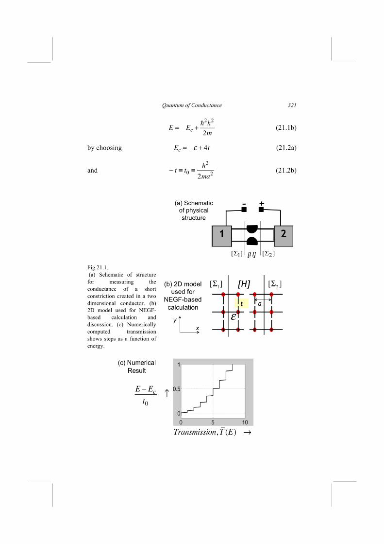
Quantum of Conductance
321
E = Ec +2k2
2m (21.1b)
by choosing Ec= ε + 4t (21.2a)
and
− t ≡ t0 ≡2
2ma2
(21.2b)
Fig.21.1. (a) Schematic of structure for measuring the conductance of a short constriction created in a two dimensional conductor. (b) 2D model used for NEGF-based calculation and discussion. (c) Numerically computed transmission shows steps as a function of energy.
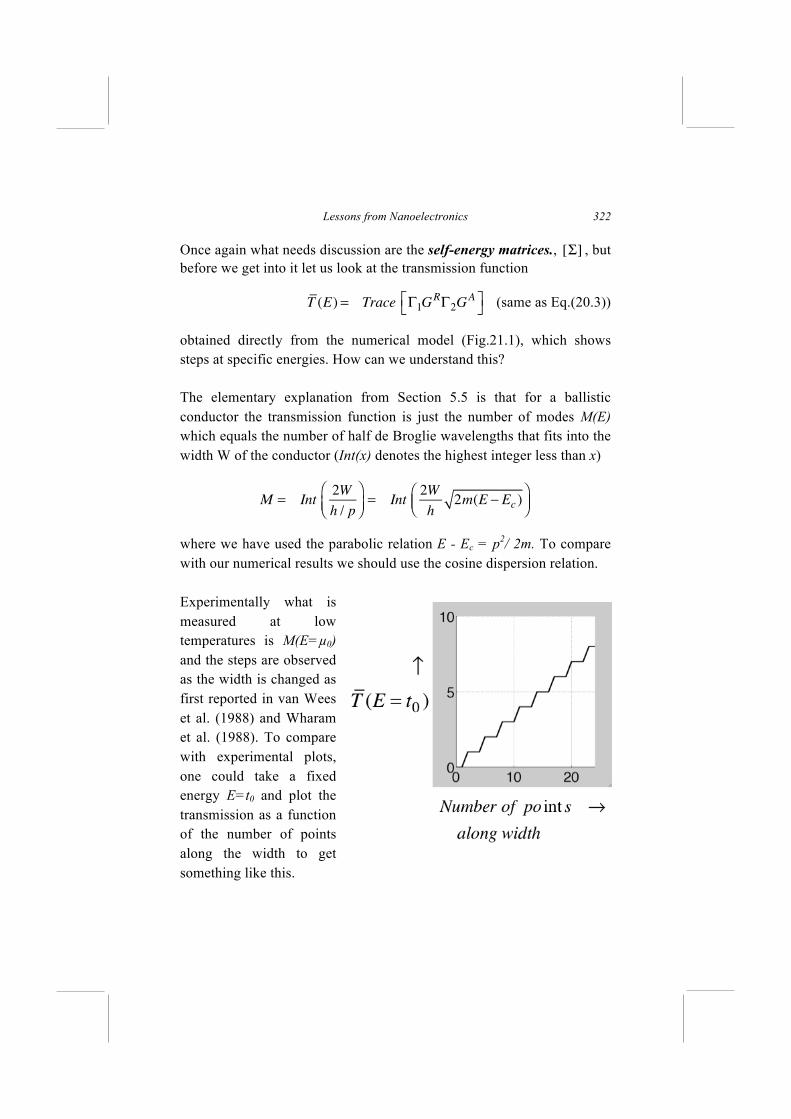
Lessons from Nanoelectronics
322
Once again what needs discussion are the self-energy matrices., [Σ] , but before we get into it let us look at the transmission function
T (E) = Trace Γ1GRΓ2G
A⎡⎣
⎤⎦ (same as Eq.(20.3))
obtained directly from the numerical model (Fig.21.1), which shows steps at specific energies. How can we understand this? The elementary explanation from Section 5.5 is that for a ballistic conductor the transmission function is just the number of modes M(E) which equals the number of half de Broglie wavelengths that fits into the width W of the conductor (Int(x) denotes the highest integer less than x)
M = Int2W
h / p
⎛⎝⎜
⎞⎠⎟= Int
2W
h2m(E − Ec )
⎛⎝⎜
⎞⎠⎟
where we have used the parabolic relation E - Ec = p2/ 2m. To compare with our numerical results we should use the cosine dispersion relation. Experimentally what is measured at low temperatures is M(E=µ0) and the steps are observed as the width is changed as first reported in van Wees et al. (1988) and Wharam et al. (1988). To compare with experimental plots, one could take a fixed energy E=t0 and plot the transmission as a function of the number of points along the width to get something like this.
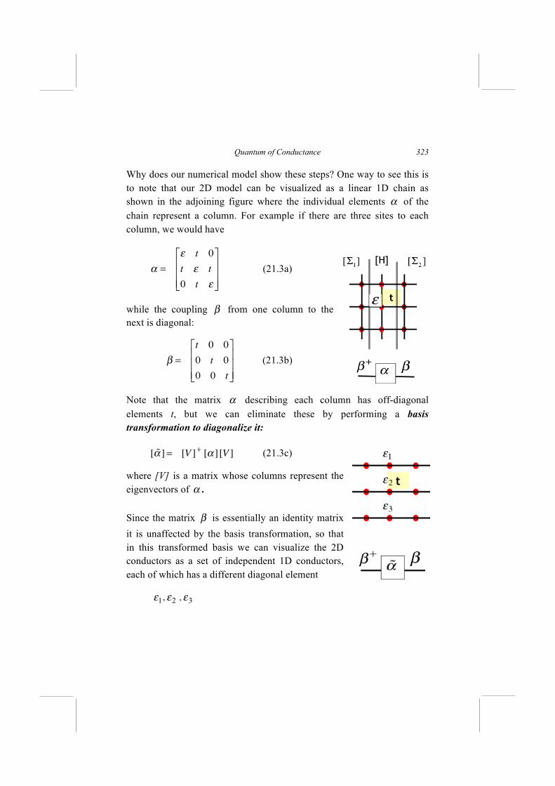
Quantum of Conductance
323
Why does our numerical model show these steps? One way to see this is to note that our 2D model can be visualized as a linear 1D chain as shown in the adjoining figure where the individual elements α of the chain represent a column. For example if there are three sites to each column, we would have
α =
ε t 0
t ε t
0 t ε
⎡
⎣
⎢⎢⎢
⎤
⎦
⎥⎥⎥
(21.3a)
while the coupling β from one column to the next is diagonal:
β =
t 0 0
0 t 0
0 0 t
⎡
⎣
⎢⎢⎢
⎤
⎦
⎥⎥⎥
(21.3b)
Note that the matrix α describing each column has off-diagonal elements t, but we can eliminate these by performing a basis transformation to diagonalize it:
[ α ] = [V ]
+[α ] [V ] (21.3c)
where [V] is a matrix whose columns represent the eigenvectors of α . Since the matrix β is essentially an identity matrix it is unaffected by the basis transformation, so that in this transformed basis we can visualize the 2D conductors as a set of independent 1D conductors, each of which has a different diagonal element
ε1, ε2 , ε3
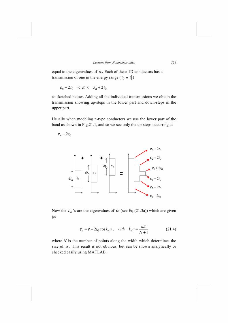
Lessons from Nanoelectronics
324
equal to the eigenvalues of α . Each of these 1D conductors has a transmission of one in the energy range ( t0 ≡ t )
εn− 2 t0 < E < ε
n+ 2 t0
as sketched below. Adding all the individual transmissions we obtain the transmission showing up-steps in the lower part and down-steps in the upper part. Usually when modeling n-type conductors we use the lower part of the band as shown in Fig.21.1, and so we see only the up-steps occurring at
εn− 2 t0
Now the ε
n’s are the eigenvalues of α (see Eq.(21.3a)) which are given
by
εn = ε − 2t0 coskna , with kna =nπ
N +1 (21.4)
where N is the number of points along the width which determines the size of α . This result is not obvious, but can be shown analytically or checked easily using MATLAB.
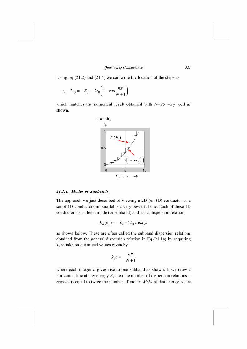
Quantum of Conductance
325
Using Eq.(21.2) and (21.4) we can write the location of the steps as
εn − 2t0 = Ec + 2t0 1− cos
nπN +1
⎛⎝⎜
⎞⎠⎟
which matches the numerical result obtained with N=25 very well as shown.
21.1.1. Modes or Subbands
The approach we just described of viewing a 2D (or 3D) conductor as a set of 1D conductors in parallel is a very powerful one. Each of these 1D conductors is called a mode (or subband) and has a dispersion relation
En (kx ) = εn − 2t0 coskxa
as shown below. These are often called the subband dispersion relations obtained from the general dispersion relation in Eq.(21.1a) by requiring ky to take on quantized values given by
kya =nπ
N +1
where each integer n gives rise to one subband as shown. If we draw a horizontal line at any energy E, then the number of dispersion relations it crosses is equal to twice the number of modes M(E) at that energy, since
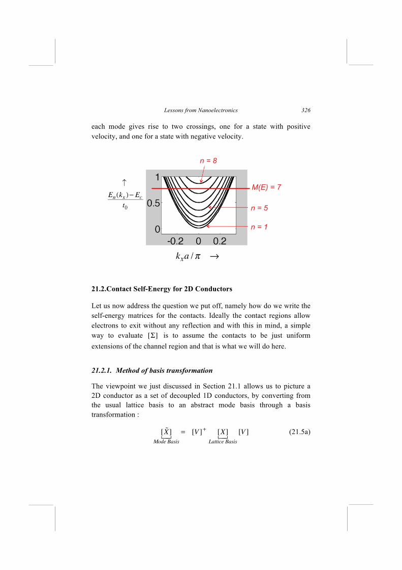
Lessons from Nanoelectronics
326
each mode gives rise to two crossings, one for a state with positive velocity, and one for a state with negative velocity.
21.2.Contact Self-Energy for 2D Conductors
Let us now address the question we put off, namely how do we write the self-energy matrices for the contacts. Ideally the contact regions allow electrons to exit without any reflection and with this in mind, a simple way to evaluate [Σ] is to assume the contacts to be just uniform extensions of the channel region and that is what we will do here.
21.2.1. Method of basis transformation
The viewpoint we just discussed in Section 21.1 allows us to picture a 2D conductor as a set of decoupled 1D conductors, by converting from the usual lattice basis to an abstract mode basis through a basis transformation :
[ X]
Mode Basis
= [V ]
+[X]
Lattice Basis
[V ] (21.5a)
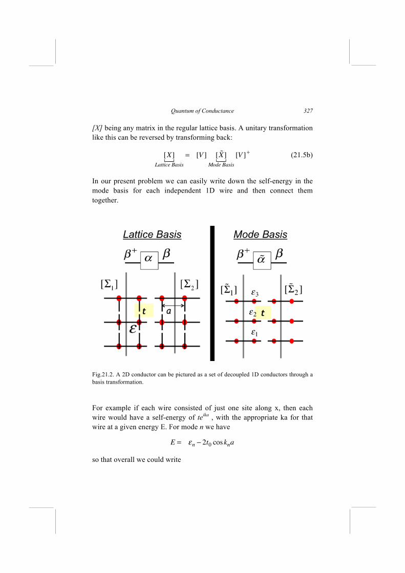
Quantum of Conductance
327
[X] being any matrix in the regular lattice basis. A unitary transformation like this can be reversed by transforming back:
[X]
Lattice Basis
= [V ] [ X]
Mode Basis
[V ]
+ (21.5b)
In our present problem we can easily write down the self-energy in the mode basis for each independent 1D wire and then connect them together.
Fig.21.2. A 2D conductor can be pictured as a set of decoupled 1D conductors through a basis transformation. For example if each wire consisted of just one site along x, then each wire would have a self-energy of teika , with the appropriate ka for that wire at a given energy E. For mode n we have
E = εn − 2t0 coskna
so that overall we could write
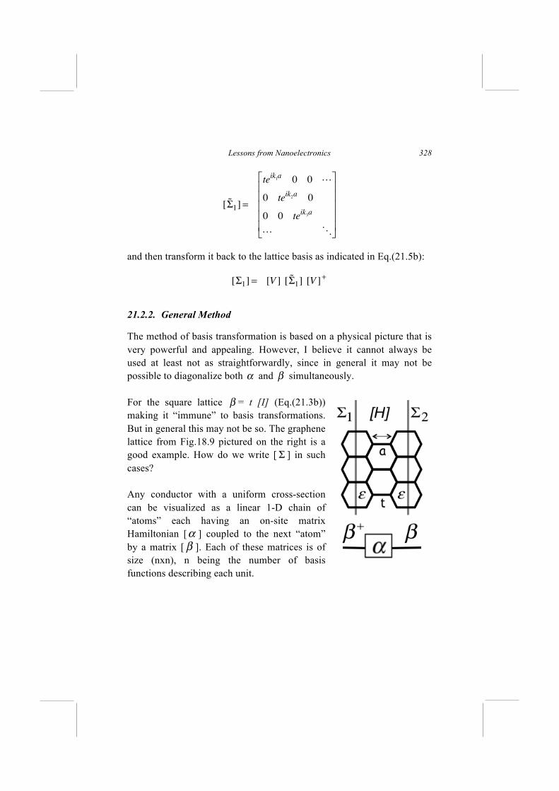
Lessons from Nanoelectronics
328
[ Σ1] =
teik1a0 0
0 teik2a0
0 0 teik3a
⎡
⎣
⎢⎢⎢⎢⎢
⎤
⎦
⎥⎥⎥⎥⎥
and then transform it back to the lattice basis as indicated in Eq.(21.5b):
[Σ1] = [V ] [ Σ1] [V ]
+
21.2.2. General Method
The method of basis transformation is based on a physical picture that is very powerful and appealing. However, I believe it cannot always be used at least not as straightforwardly, since in general it may not be possible to diagonalize both α and β simultaneously. For the square lattice β = t [I] (Eq.(21.3b)) making it “immune” to basis transformations. But in general this may not be so. The graphene lattice from Fig.18.9 pictured on the right is a good example. How do we write [ Σ ] in such cases? Any conductor with a uniform cross-section can be visualized as a linear 1-D chain of “atoms” each having an on-site matrix Hamiltonian [ ] coupled to the next “atom” by a matrix [ ]. Each of these matrices is of size (nxn), n being the number of basis functions describing each unit.
α
β
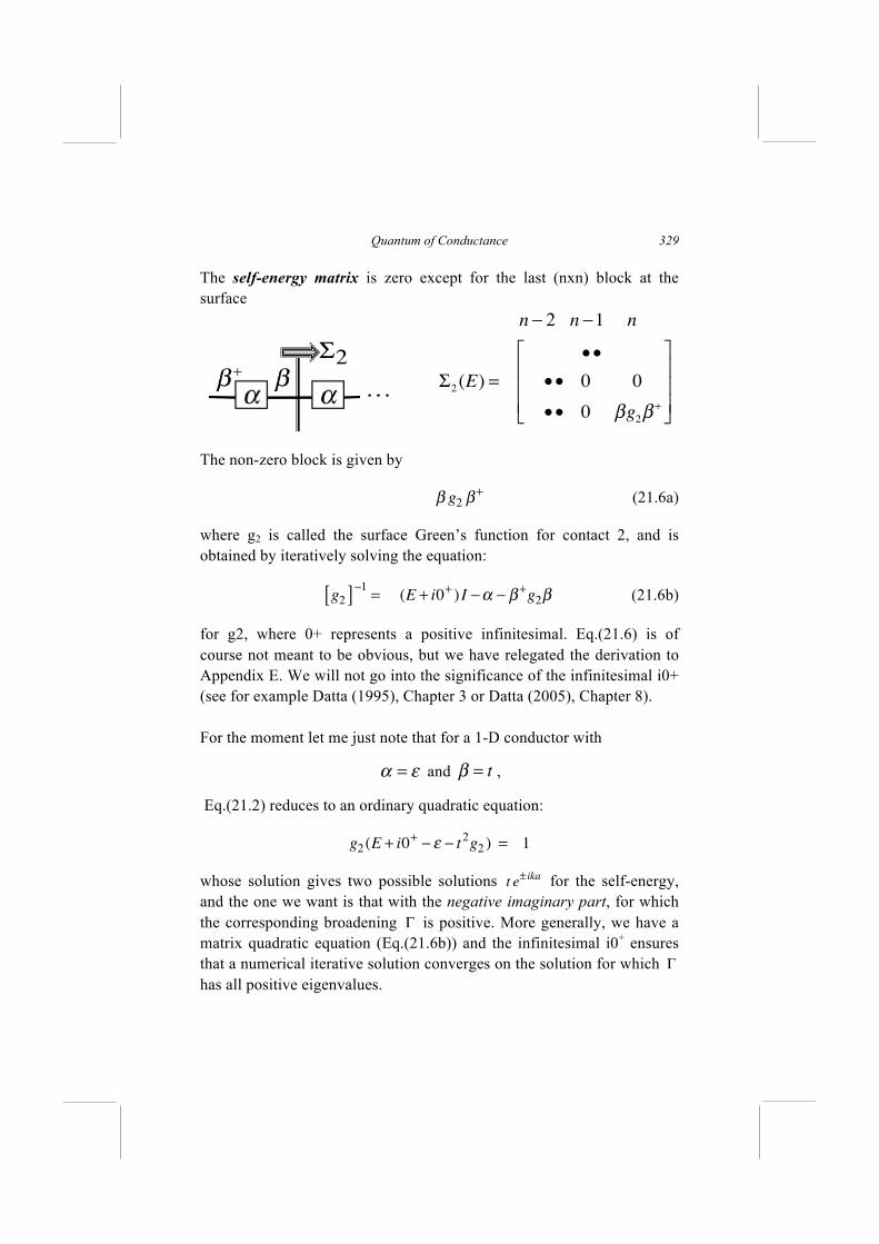
Quantum of Conductance
329
The self-energy matrix is zero except for the last (nxn) block at the surface
The non-zero block is given by
β g2 β+ (21.6a)
where g2 is called the surface Green’s function for contact 2, and is obtained by iteratively solving the equation:
g2[ ]−1
= (E + i0+) I −α − β+
g2β (21.6b)
for g2, where 0+ represents a positive infinitesimal. Eq.(21.6) is of course not meant to be obvious, but we have relegated the derivation to Appendix E. We will not go into the significance of the infinitesimal i0+ (see for example Datta (1995), Chapter 3 or Datta (2005), Chapter 8). For the moment let me just note that for a 1-D conductor with
and ,
Eq.(21.2) reduces to an ordinary quadratic equation:
g2(E + i0+− ε − t
2g2 ) = 1
whose solution gives two possible solutions t e± ika for the self-energy, and the one we want is that with the negative imaginary part, for which the corresponding broadening Γ is positive. More generally, we have a matrix quadratic equation (Eq.(21.6b)) and the infinitesimal i0+ ensures that a numerical iterative solution converges on the solution for which Γ has all positive eigenvalues.
α = ε β = t
n − 2 n −1 n
Σ2(E) =
••
•• 0 0
•• 0 βg2β +
⎡
⎣
⎢⎢⎢
⎤
⎦
⎥⎥⎥
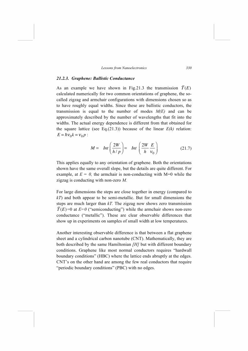
Lessons from Nanoelectronics
330
21.2.3. Graphene: Ballistic Conductance
As an example we have shown in Fig.21.3 the transmission T (E) calculated numerically for two common orientations of graphene, the so-called zigzag and armchair configurations with dimensions chosen so as to have roughly equal widths. Since these are ballistic conductors, the transmission is equal to the number of modes M(E) and can be approximately described by the number of wavelengths that fit into the widths. The actual energy dependence is different from that obtained for the square lattice (see Eq.(21.3)) because of the linear E(k) relation:
E = ν0k = ν0p :
M = Int2W
h / p
⎛⎝⎜
⎞⎠⎟= Int
2W
h
E
ν0
⎛⎝⎜
⎞⎠⎟
(21.7)
This applies equally to any orientation of graphene. Both the orientations shown have the same overall slope, but the details are quite different. For example, at E = 0, the armchair is non-conducting with M=0 while the zigzag is conducting with non-zero M. For large dimensions the steps are close together in energy (compared to kT) and both appear to be semi-metallic. But for small dimensions the steps are much larger than kT. The zigzag now shows zero transmission T (E)=0 at E=0 (“semiconducting”) while the armchair shows non-zero conductance (“metallic”). These are clear observable differences that show up in experiments on samples of small width at low temperatures. Another interesting observable difference is that between a flat graphene sheet and a cylindrical carbon nanotube (CNT). Mathematically, they are both described by the same Hamiltonian [H] but with different boundary conditions. Graphene like most normal conductors requires “hardwall boundary conditions” (HBC) where the lattice ends abruptly at the edges. CNT’s on the other hand are among the few real conductors that require “periodic boundary conditions” (PBC) with no edges.
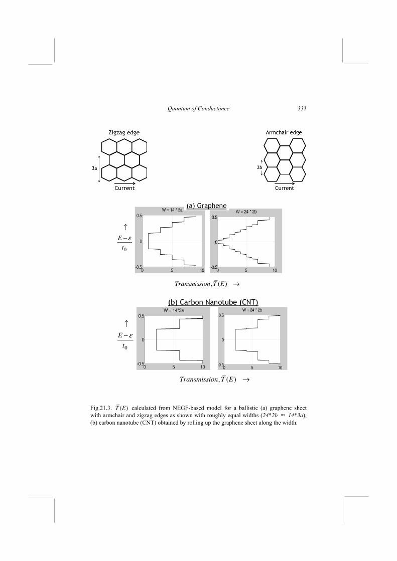
Quantum of Conductance
331
Fig.21.3. T (E) calculated from NEGF-based model for a ballistic (a) graphene sheet with armchair and zigzag edges as shown with roughly equal widths (24*2b ≈ 14*3a), (b) carbon nanotube (CNT) obtained by rolling up the graphene sheet along the width.
Lessons from Nanoelectronics
332
The results for CNT are relatively easy to understand analytically, while those for graphene require a more extensive discussion. (see for example Brey and Fertig, 2006). As we mentioned in Lecture 5, PBC is mathematically simpler and that is why it is used so extensively for large conductors where it is known experimentally that the exact boundary conditions are not very relevant. But this of course is not true of small conductors and the difference is evident in Fig.21.2 for small conductors only a few nanometers in width. We will not go into this further. Our objective here is simply to show how easily our quantum transport formalism captures all the known physics. The power of the numerical method lies in being able to calculate M(E) automatically even before one has “understood” the results. However, one should use numerical calculations not as a substitute for understanding , but as an aid to understanding.
21.3.Quantum Hall Effect
The Hall effect (Lecture 13) provides another good example for a two-dimensional application of the quantum transport model. The basic structure involves a long conductor with side probes designed to measure the transverse Hall voltage developed in the presence of a magnetic field. We use the same 2D Hamiltonian from Fig.21.1 but now including a magnetic field as explained in Section 18.4.3. As discussed in Lecture 13, the Hall resistance is given by the ratio of the Hall voltage to the current. In a theoretical model we could calculate the Hall voltage in one of two ways. We could attach a voltage probe to each side and use Büttiker’s multiterminal method to find the potentials they float to. Alternatively we could do what we explained in Section 20.3, namely calculate the fractional occupation of the states at any point j by looking at the ratio of the diagonal element of the electron density Gn and the density of states A and use the low bias Taylor expansion (Eq.(2.8)) to translate the occupation factor profile into a potential profile.
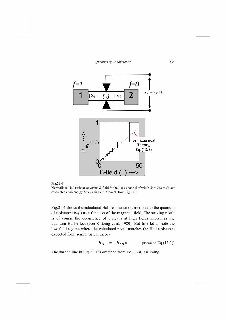
Quantum of Conductance
333
Fig.21.4 Normalized Hall resistance versus B-field for ballistic channel of width W = 26a = 65 nm calculated at an energy E=t 0 using a 2D model from Fig.21.1. Fig.21.4 shows the calculated Hall resistance (normalized to the quantum of resistance h/q2) as a function of the magnetic field. The striking result is of course the occurrence of plateaus at high fields known as the quantum Hall effect (von Klitzing et al. 1980). But first let us note the low field regime where the calculated result matches the Hall resistance expected from semiclassical theory
RH = B / qn (same as Eq.(13.3))
The dashed line in Fig.21.3 is obtained from Eq.(13.4) assuming
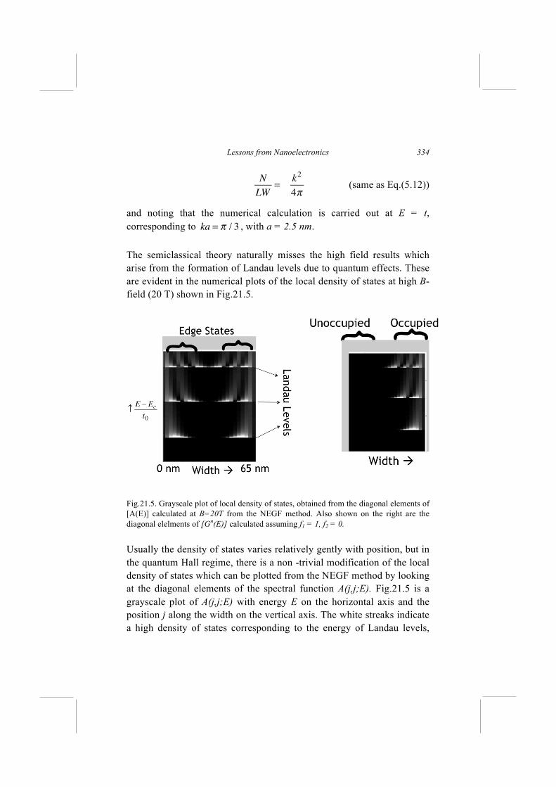
Lessons from Nanoelectronics
334
N
LW=
k2
4π (same as Eq.(5.12))
and noting that the numerical calculation is carried out at E = t, corresponding to ka = π / 3 , with a = 2.5 nm. The semiclassical theory naturally misses the high field results which arise from the formation of Landau levels due to quantum effects. These are evident in the numerical plots of the local density of states at high B-field (20 T) shown in Fig.21.5.
Fig.21.5. Grayscale plot of local density of states, obtained from the diagonal elements of [A(E)] calculated at B=20T from the NEGF method. Also shown on the right are the diagonal elelments of [Gn(E)] calculated assuming f1 = 1, f2 = 0. Usually the density of states varies relatively gently with position, but in the quantum Hall regime, there is a non -trivial modification of the local density of states which can be plotted from the NEGF method by looking at the diagonal elements of the spectral function A(j,j;E). Fig.21.5 is a grayscale plot of A(j,j;E) with energy E on the horizontal axis and the position j along the width on the vertical axis. The white streaks indicate a high density of states corresponding to the energy of Landau levels,
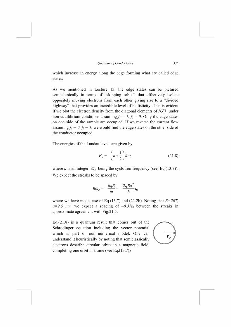
Quantum of Conductance
335
which increase in energy along the edge forming what are called edge states. As we mentioned in Lecture 13, the edge states can be pictured semiclassically in terms of “skipping orbits” that effectively isolate oppositely moving electrons from each other giving rise to a “divided highway” that provides an incredible level of ballisticity. This is evident if we plot the electron density from the diagonal elements of [Gn] under non-equilibrium conditions assuming f1 = 1, f2 = 0. Only the edge states on one side of the sample are occupied. If we reverse the current flow assuming f1 = 0, f2 = 1, we would find the edge states on the other side of the conductor occupied. The energies of the Landau levels are given by
En= n +
1
2
⎛⎝⎜
⎞⎠⎟ω
c (21.8)
where n is an integer, ωc
being the cyclotron frequency (see Eq.(13.7)). We expect the streaks to be spaced by
ωc =qB
m=
2qBa2
t0
where we have made use of Eq.(13.7) and (21.2b). Noting that B=20T, a=2.5 nm, we expect a spacing of ~0.37t0 between the streaks in approximate agreement with Fig.21.5. Eq.(21.8) is a quantum result that comes out of the Schrödinger equation including the vector potential which is part of our numerical model. One can understand it heuristically by noting that semiclassically electrons describe circular orbits in a magnetic field, completing one orbit in a time (see Eq.(13.7))
Lessons from Nanoelectronics
336
tc =2π
ωc
=2π p
qνB
so that the circumference of one orbit of radius rc is given by
2πrc = νtc =2π p
qB
If we now impose the quantum requirement that the circumference equal an integer number of de Broglie wavelengths h/p, we have
2π p
qB= integer *
h
p
Semiclassically an electron can have any energy E = p2/2m. But the need to fit an integer number of wavelengths leads to the condition that
p2
= integer * hqB
suggesting that the allowed energies should be given by
E = integer *hqB
2m= integer *
ωc
2
which is not exactly the correct answer (Eq.(21.8)), but close enough for a heuristic argument. The resulting current equals
q2
hV Number of Edge States( )
while the Hall voltage simply equals the applied voltage since one edge of the sample is in equilibrium with the source and other with the drain.
Quantum of Conductance
337
This leads to a quantized Hall resistance given by
h
q2
1
Number of Edge States
giving rise to the plateaus of 1/4, 1/3, 1/2, 1 seen in Fig.21.4, as the magnetic field raises the Landau levels, changing the number of edge states at an energy E=t0 from 4 to 3 to 2 to 1. I should mention that the theoretical model does not include the two spins and so gives a resistance that is twice as large as the experimentally observed values which look more like
h
2q2
1
Number of Edge States
because edge states usually come in pairs, except at high B-fields. Also, we have not talked at all about the fractional quantum Hall effect observed in pure samples at larger B-fields with Hall resistances that look like
h
q2
1
a fraction
This is a vast and rich area of research on its own beyond the scope of the simple NEGF model discussed here. As it stands it captures only the integer Hall effect though innovative extensions could take it beyond this regime.
Lessons from Nanoelectronics
338
Lecture 22
Rotating an electron
22.1. One-level Spin Valve 22.2. Rotating Magnetic Contacts 22.3. Spin Hamiltonians 22.4. Vectors and Spinors 22.5. Spin Precession 22.6. From NEGF to Diffusion
Back in Lecture 14, we discussed how magnets can be used to create spin potentials inside a non-magnetic channel that extend even outside the path of the current and can be measured using another magnetic voltage probe with a polarization
P (Fig.22.1). This led naturally to the concept
of a charge potential µ and a spin potential µs such that
µprobe = µ +Pµs
2
At the end of the Lecture we stated the more general result
µprobe = µ +
P.µs
2 (22.1)
that can be used even when the magnet polarization
P and the spin
potential
µs in the channel are not collinear.
I am not sure if anyone has actually done the experiment shown in Fig.22.1, namely inject spins with a fixed magnet and measure the voltage with a magnet whose direction is rotated. What has been done, however, is to keep both magnets fixed and rotate the electron spin inside
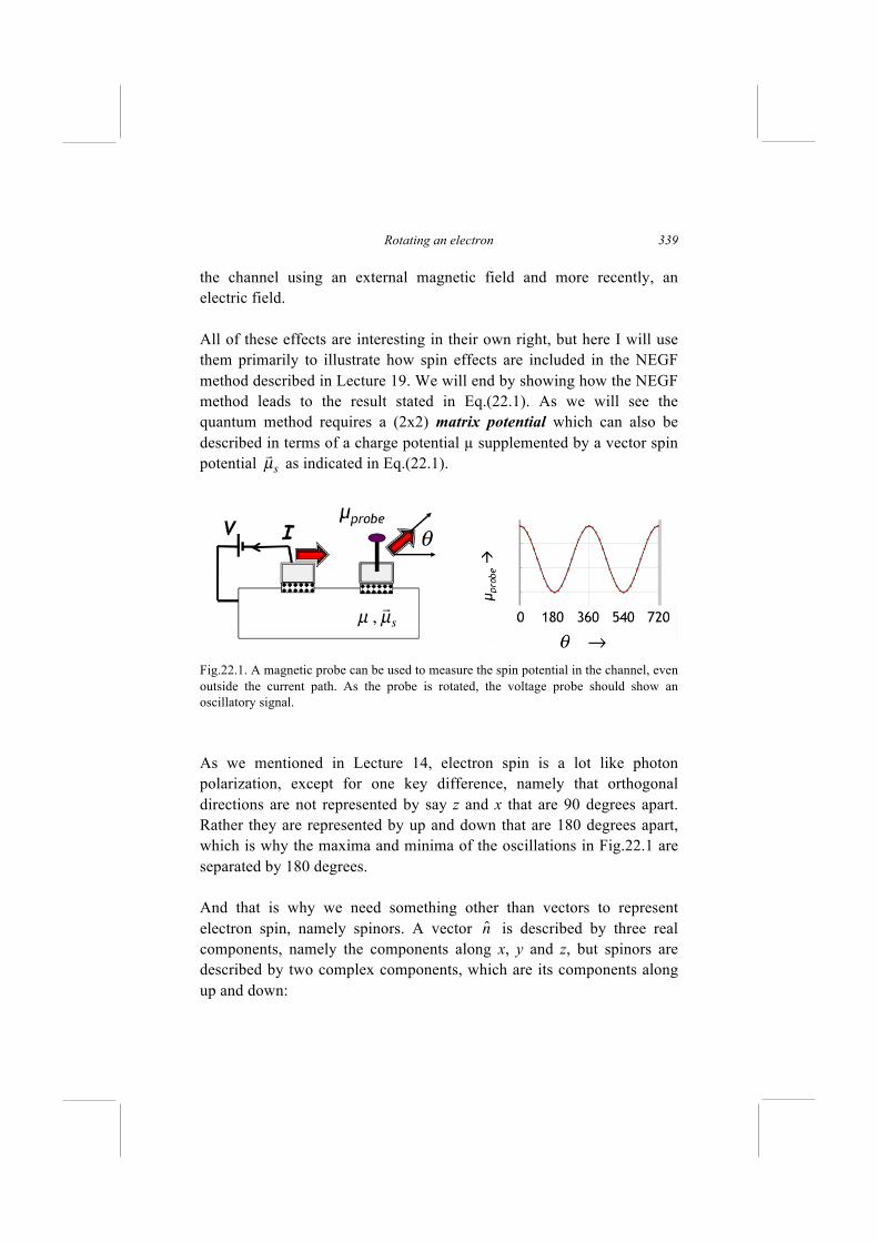
Rotating an electron
339
the channel using an external magnetic field and more recently, an electric field. All of these effects are interesting in their own right, but here I will use them primarily to illustrate how spin effects are included in the NEGF method described in Lecture 19. We will end by showing how the NEGF method leads to the result stated in Eq.(22.1). As we will see the quantum method requires a (2x2) matrix potential which can also be described in terms of a charge potential µ supplemented by a vector spin potential
µs as indicated in Eq.(22.1).
Fig.22.1. A magnetic probe can be used to measure the spin potential in the channel, even outside the current path. As the probe is rotated, the voltage probe should show an oscillatory signal. As we mentioned in Lecture 14, electron spin is a lot like photon polarization, except for one key difference, namely that orthogonal directions are not represented by say z and x that are 90 degrees apart. Rather they are represented by up and down that are 180 degrees apart, which is why the maxima and minima of the oscillations in Fig.22.1 are separated by 180 degrees. And that is why we need something other than vectors to represent electron spin, namely spinors. A vector n is described by three real components, namely the components along x, y and z, but spinors are described by two complex components, which are its components along up and down:
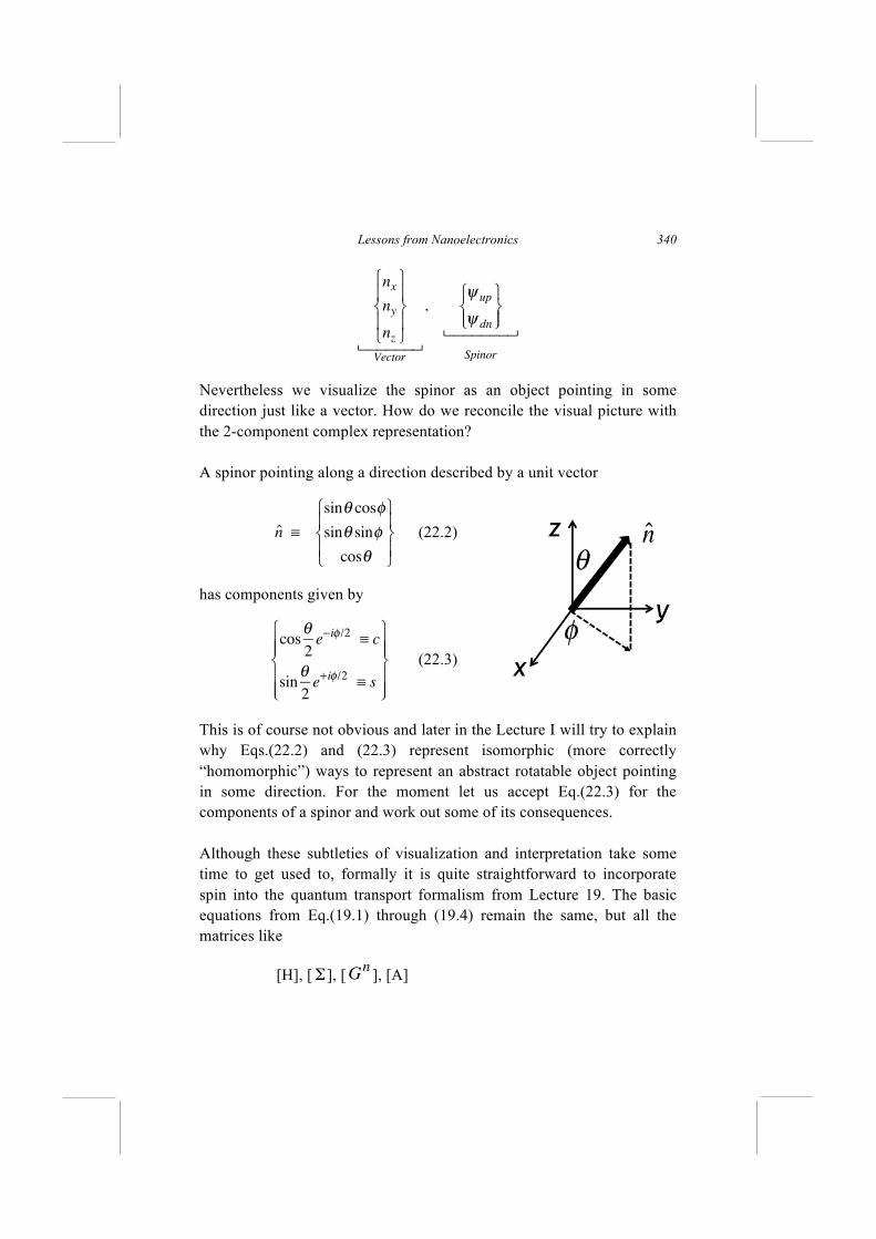
Lessons from Nanoelectronics
340
nx
ny
nz
⎧
⎨⎪
⎩⎪
⎫
⎬⎪
⎭⎪
Vector
,ψ up
ψ dn
⎧⎨⎩⎪
⎫⎬⎭⎪
Spinor
Nevertheless we visualize the spinor as an object pointing in some direction just like a vector. How do we reconcile the visual picture with the 2-component complex representation? A spinor pointing along a direction described by a unit vector
n ≡
sinθ cosφ
sinθ sinφ
cosθ
⎧
⎨⎪
⎩⎪
⎫
⎬⎪
⎭⎪
(22.2)
has components given by
cos
θ2e−iφ /2 ≡ c
sinθ2e+iφ /2 ≡ s
⎧
⎨⎪⎪
⎩⎪⎪
⎫
⎬⎪⎪
⎭⎪⎪
(22.3)
This is of course not obvious and later in the Lecture I will try to explain why Eqs.(22.2) and (22.3) represent isomorphic (more correctly “homomorphic”) ways to represent an abstract rotatable object pointing in some direction. For the moment let us accept Eq.(22.3) for the components of a spinor and work out some of its consequences. Although these subtleties of visualization and interpretation take some time to get used to, formally it is quite straightforward to incorporate spin into the quantum transport formalism from Lecture 19. The basic equations from Eq.(19.1) through (19.4) remain the same, but all the matrices like
[H], [ ], [ ], [A]
€
Σ
€
Gn
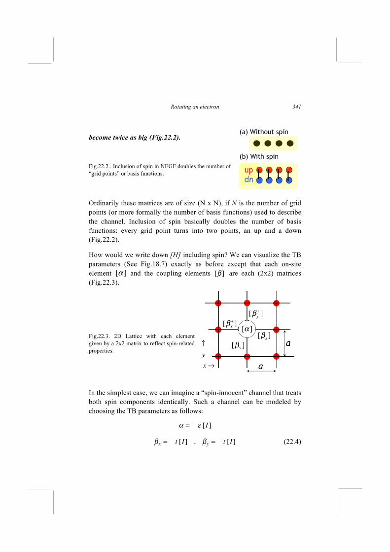
Rotating an electron
341
become twice as big (Fig.22.2).
Fig.22.2.. Inclusion of spin in NEGF doubles the number of “grid points” or basis functions.
Ordinarily these matrices are of size (N x N), if N is the number of grid points (or more formally the number of basis functions) used to describe the channel. Inclusion of spin basically doubles the number of basis functions: every grid point turns into two points, an up and a down (Fig.22.2).
How would we write down [H] including spin? We can visualize the TB parameters (See Fig.18.7) exactly as before except that each on-site element and the coupling elements [β ] are each (2x2) matrices (Fig.22.3).
Fig.22.3. 2D Lattice with each element given by a 2x2 matrix to reflect spin-related properties.
In the simplest case, we can imagine a “spin-innocent” channel that treats both spin components identically. Such a channel can be modeled by choosing the TB parameters as follows:
α = ε [I ]
βx = t [I ] , βy = t [I ] (22.4)
[α ]
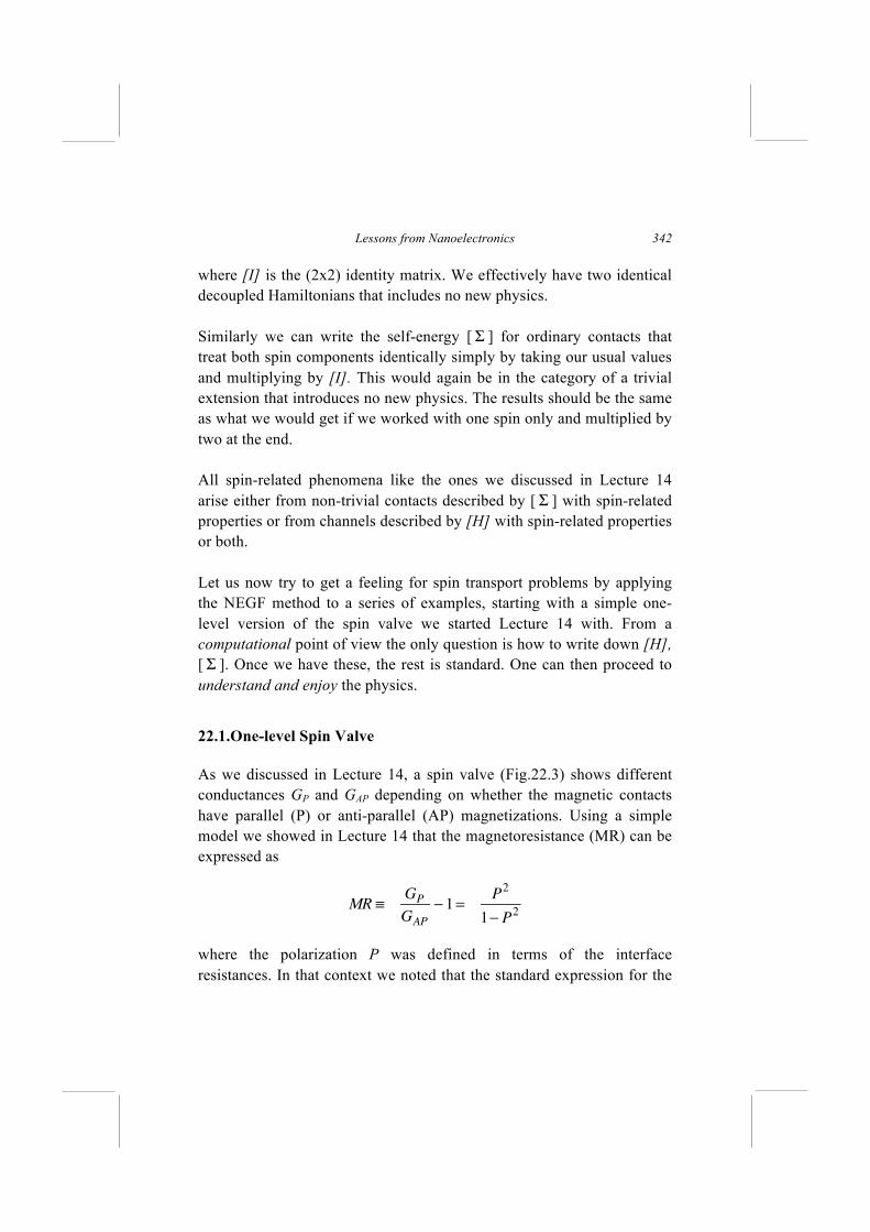
Lessons from Nanoelectronics
342
where [I] is the (2x2) identity matrix. We effectively have two identical decoupled Hamiltonians that includes no new physics. Similarly we can write the self-energy [ Σ ] for ordinary contacts that treat both spin components identically simply by taking our usual values and multiplying by [I]. This would again be in the category of a trivial extension that introduces no new physics. The results should be the same as what we would get if we worked with one spin only and multiplied by two at the end. All spin-related phenomena like the ones we discussed in Lecture 14 arise either from non-trivial contacts described by [ Σ ] with spin-related properties or from channels described by [H] with spin-related properties or both. Let us now try to get a feeling for spin transport problems by applying the NEGF method to a series of examples, starting with a simple one-level version of the spin valve we started Lecture 14 with. From a computational point of view the only question is how to write down [H], [ Σ ]. Once we have these, the rest is standard. One can then proceed to understand and enjoy the physics.
22.1.One-level Spin Valve
As we discussed in Lecture 14, a spin valve (Fig.22.3) shows different conductances GP and GAP depending on whether the magnetic contacts have parallel (P) or anti-parallel (AP) magnetizations. Using a simple model we showed in Lecture 14 that the magnetoresistance (MR) can be expressed as
MR ≡GP
GAP
− 1=P2
1− P2
where the polarization P was defined in terms of the interface resistances. In that context we noted that the standard expression for the
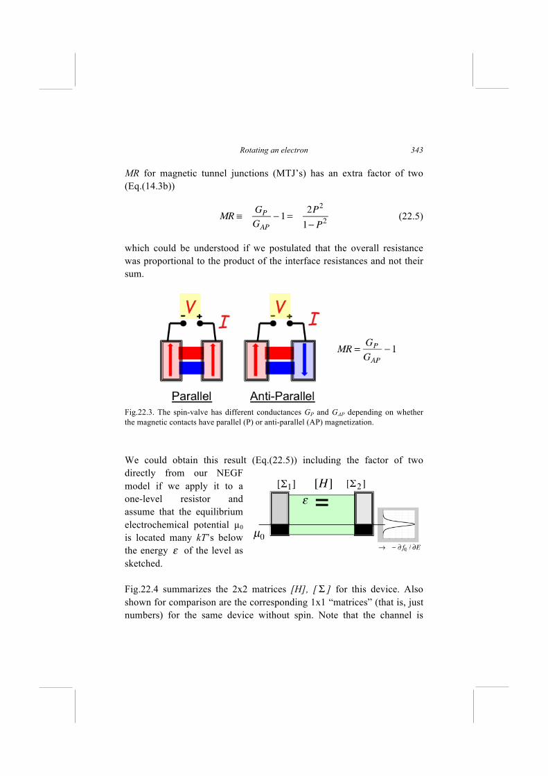
Rotating an electron
343
MR for magnetic tunnel junctions (MTJ’s) has an extra factor of two (Eq.(14.3b))
MR ≡GP
GAP
− 1=2P
2
1− P2
(22.5)
which could be understood if we postulated that the overall resistance was proportional to the product of the interface resistances and not their sum.
Fig.22.3. The spin-valve has different conductances GP and GAP depending on whether the magnetic contacts have parallel (P) or anti-parallel (AP) magnetization. We could obtain this result (Eq.(22.5)) including the factor of two directly from our NEGF model if we apply it to a one-level resistor and assume that the equilibrium electrochemical potential µ0 is located many kT’s below the energy ε of the level as sketched. Fig.22.4 summarizes the 2x2 matrices [H], [ Σ ] for this device. Also shown for comparison are the corresponding 1x1 “matrices” (that is, just numbers) for the same device without spin. Note that the channel is
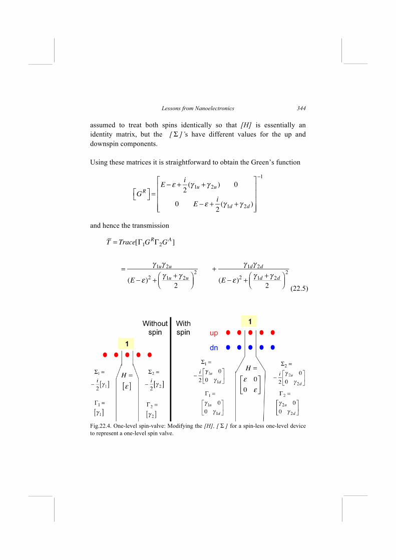
Lessons from Nanoelectronics
344
assumed to treat both spins identically so that [H] is essentially an identity matrix, but the [ Σ ]’s have different values for the up and downspin components.
Using these matrices it is straightforward to obtain the Green’s function
GR⎡
⎣⎤⎦ =
E − ε +i
2(γ 1u + γ 2u ) 0
0 E − ε +i
2(γ 1d + γ 2d )
⎡
⎣
⎢⎢⎢⎢
⎤
⎦
⎥⎥⎥⎥
−1
and hence the transmission
T = Trace[Γ1GRΓ2G
A]
=γ 1uγ 2u
(E − ε )2 +γ 1u + γ 2u
2
⎛⎝⎜
⎞⎠⎟2
+γ 1dγ 2d
(E − ε )2 +γ 1d + γ 2d
2
⎛⎝⎜
⎞⎠⎟2
(22.5)
Fig.22.4. One-level spin-valve: Modifying the [H], [ Σ ] for a spin-less one-level device to represent a one-level spin valve.
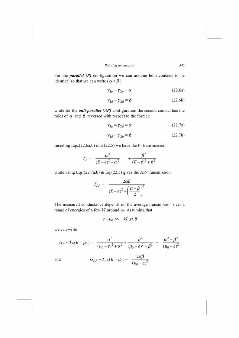
Rotating an electron
345
For the parallel (P) configuration we can assume both contacts to be identical so that we can write (α > β )
γ 1u = γ 2u =α (22.6a)
γ 1d = γ 2d ≡ β (22.6b)
while for the anti-parallel (AP) configuration the second contact has the roles of α and β reversed with respect to the former:
γ 1u = γ 2d =α (22.7a)
γ 1d = γ 2u ≡ β (22.7b)
Inserting Eqs.(22.6a,b) into (22.5) we have the P- transmission
TP=
α 2
(E − ε )2 +α 2+
β 2
(E − ε )2 + β 2
while using Eqs.(22.7a,b) in Eq.(22.5) gives the AP- transmission
TAP =2αβ
(E − ε )2 +α + β2
⎛⎝⎜
⎞⎠⎟2
The measured conductance depends on the average transmission over a range of energies of a few kT around µ0. Assuming that
ε − µ0 >> kT ,α ,β
we can write
GP ~ TP (E = µ0 ) =α 2
(µ0 − ε )2+α 2
+β 2
(µ0 − ε )2+ β 2
≈ α 2 + β 2
(µ0 − ε )2
and GAP ~ TAP (E = µ0 ) ≈2αβ
(µ0 − ε )2
Lessons from Nanoelectronics
346
This gives us
MR ≡GP
GAp
−1=α 2 + β 2
2αβ−1=
2P2
1− P2
as stated earlier in Eq.(22.5) with the polarization defined as
P ≡α − β
α + β (22.8)
Actually we could also obtain the result (Eq.(14.3a)) obtained from the resistor model in Lecture 14, if we assume that µ0 is located right around the level ε , with kT >> α , β . But we leave that as an exercise. After all this is just a toy problem intended to get us started.
22.2. Rotating Magnetic Contacts
We argued in the last Section that for an anti-parallel spin valve, the second contact simply has the roles of α and β reversed relative to the first, so that we can write
Γ1 =α 0
0 β⎡
⎣⎢
⎤
⎦⎥ , Γ2 =
β 0
0 α⎡
⎣⎢
⎤
⎦⎥
But how would we write the corresponding matrix for a contact if it were pointing along some arbitrary direction defined by a unit vector n ? The answer is
Γ =α + β2
[I ] +α − β2
nz nx − inynx + iny − nz
⎡
⎣⎢⎢
⎤
⎦⎥⎥
(22.9)
where nx , ny , nz are the components of the unit vector n along x, y and z respectively. This result is of course not obvious and we will try to justify it shortly. But it is reassuring to note that the results for both the parallel and the anti-parallel contact come out as special cases of this general result (Eq.(22.9)):
Rotating an electron
347
If nz = +1, nx = ny = 0 : Γ =α 0
0 β⎡
⎣⎢
⎤
⎦⎥
If nz = −1, nx = ny = 0 : Γ =β 0
0 α⎡
⎣⎢
⎤
⎦⎥
One way to understand where Eq.(22.9) comes from is to note that the appropriate matrix describing a magnet pointing along n would be
Γ =α 0
0 β⎡
⎣⎢
⎤
⎦⎥ (22.10)
if we were to take + n and - n as our reference directions instead of + zand - z as we normally do. How could we then transform the Γ from Eq.(22.10) into the usual ± z basis ? Answer: Transform from the ± n to the ± z basis
(22.11)
using the unitary transformation matrix [V] whose columns represent the components of a spinor pointing along ± n . The first column follows from the result we stated earlier in Eq.(22.3), while the second can be obtained from Eq.(22.3) if we set
θ → π −θ , φ→ π +φ
and remove a common phase factor from the two components.
Multiplying out the three matrices in Eq.(22.11) we have
Γ =c − s*
s c*
⎡
⎣⎢
⎤
⎦⎥α 0
0 β⎡
⎣⎢
⎤
⎦⎥c* s*
−s c
⎡
⎣⎢
⎤
⎦⎥ =
c − s*
s c*
⎡
⎣⎢
⎤
⎦⎥αc* αs*
−βs βc⎡
⎣⎢
⎤
⎦⎥
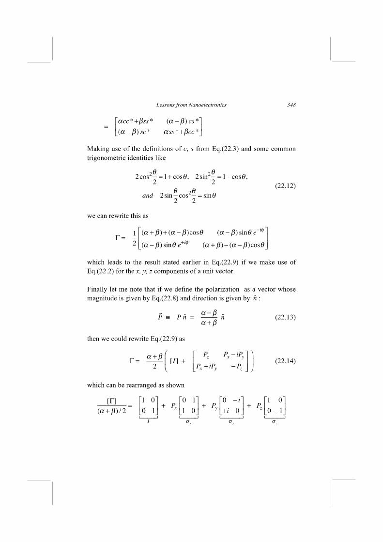
Lessons from Nanoelectronics
348
=αcc*+βss* (α − β ) cs*
(α − β ) sc* αss*+βcc*⎡
⎣⎢
⎤
⎦⎥
Making use of the definitions of c, s from Eq.(22.3) and some common trigonometric identities like
2cos
2θ
2= 1+ cosθ , 2sin
2θ
2= 1− cosθ ,
and 2sinθ
2cos
2θ
2= sinθ
(22.12)
we can rewrite this as
Γ =1
2
(α + β )+ (α − β )cosθ (α − β ) sinθ e−iφ
(α − β ) sinθ e+iφ (α + β )− (α − β )cosθ
⎡
⎣⎢⎢
⎤
⎦⎥⎥
which leads to the result stated earlier in Eq.(22.9) if we make use of Eq.(22.2) for the x, y, z components of a unit vector. Finally let me note that if we define the polarization as a vector whose magnitude is given by Eq.(22.8) and direction is given by n :
P ≡ P n =
α − β
α + βn (22.13)
then we could rewrite Eq.(22.9) as
Γ =α + β2
[I ] +Pz Px − iPy
Px + iPy − Pz
⎡
⎣⎢⎢
⎤
⎦⎥⎥
⎛
⎝⎜
⎞
⎠⎟ (22.14)
which can be rearranged as shown
[Γ](α + β ) / 2
=1 0
0 1
⎡
⎣⎢
⎤
⎦⎥
I
+ Px0 1
1 0
⎡
⎣⎢
⎤
⎦⎥
σx
+ Py0 − i
+i 0
⎡
⎣⎢
⎤
⎦⎥
σy
+ Pz1 0
0 −1⎡
⎣⎢
⎤
⎦⎥
σz
Rotating an electron
349
Any 2x2 matrix can be expressed in terms of the four matrices appearing here consist of the identity matrix [I] along with the three Pauli spin matrices
σ x ≡0 1
1 0
⎡
⎣⎢
⎤
⎦⎥ , σ y ≡
0 − i
+i 0
⎡
⎣⎢
⎤
⎦⎥ and σ z ≡
1 0
0 −1
⎡
⎣⎢
⎤
⎦⎥
(22.15)
which are widely used in the spin-related literature. Making use of the Pauli spin matrices, we could write Eq.(22.14) compactly in the form
Γ =α + β
2[I ] + [σ x ] Px + [σ y ] Py + [σ z ] Pz( )
=α + β
2[I ] + [
σ ].P( ) (22.16)
This result applies to the self-energy matrices as well. For example, if
Σ = −i
2
α 0
0 β⎡
⎣⎢
⎤
⎦⎥
in the ± n basis, then in the ± z basis it is given by
Σ = − iα + β
4[I ] − i
α − β
4[σ ].n
= − iα + β
4[I ] + [
σ ].P( )
22.3. Spin Hamiltonians
Now that we have seen how to describe contacts with spin-dependent properties, let us talk briefly about channels with spin-dependent properties.
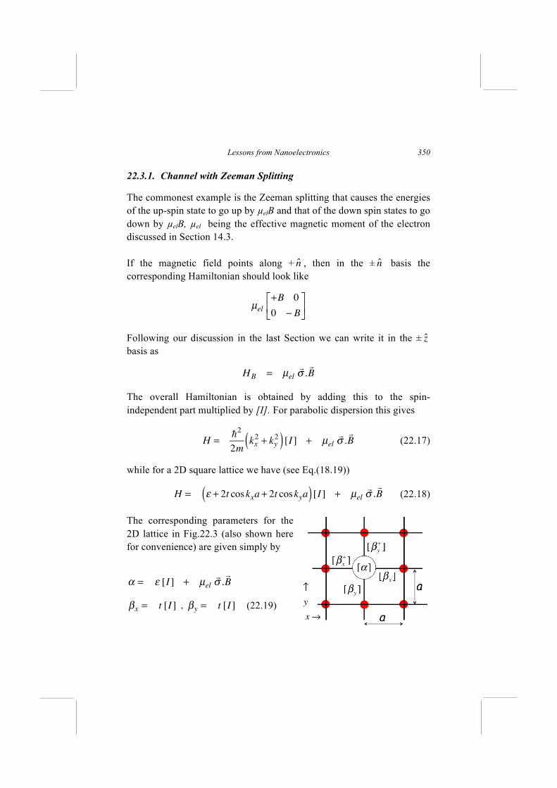
Lessons from Nanoelectronics
350
22.3.1. Channel with Zeeman Splitting
The commonest example is the Zeeman splitting that causes the energies of the up-spin state to go up by µelB and that of the down spin states to go down by µelB, µel being the effective magnetic moment of the electron discussed in Section 14.3. If the magnetic field points along + n , then in the ± n basis the corresponding Hamiltonian should look like
µel+B 0
0 − B
⎡
⎣⎢
⎤
⎦⎥
Following our discussion in the last Section we can write it in the ± z basis as
HB = µel
σ .B
The overall Hamiltonian is obtained by adding this to the spin-independent part multiplied by [I]. For parabolic dispersion this gives
H =2
2mkx2+ ky
2( ) [I ] + µelσ .B (22.17)
while for a 2D square lattice we have (see Eq.(18.19))
H = ε + 2t coskxa + 2t coskya( ) [I ] + µel
σ .B (22.18)
The corresponding parameters for the 2D lattice in Fig.22.3 (also shown here for convenience) are given simply by
α = ε [I ] + µel
σ .B
βx = t [I ] , βy = t [I ] (22.19)
Rotating an electron
351
Only the on-site parameter α is changed relative to the spin independent channel (Eq.(22.4).
22.3.2. Channel with Rashba Interaction
A more complicated example is that of the Rashba spin-orbit coupling described by a Hamiltonian of the form
HR = η z . (
σ ×k ) = η (σ xky −σ ykx ) (22.20)
whose effect has been observed in 2D surface conduction channels assumed to lie in the x-y plane. This is believed to be a relativistic effect whereby the extremely high atomic scale electric fields (that exist even at equilibrium) are perceived as an effective magnetic field by the electron and the resulting “Zeeman splitting” is described by HR. We will not go into the underlying physics of this effect any further here and simply address the question of how to include it in our 2D lattice model. With this in mind we approximate the linear terms with sine functions
HR =η
a(σ x sin kya −σ y sin kxa) (22.21)
which are written in terms of exponentials:
HR =η
2iaσ x (e
+ikya− e
−ikya) −
η
2iaσ y(e
+ikxa− e
−ikxa)
Clearly HR can be described by a Hamiltonian with
βx =iη
2aσ y , βx
+= −
iη
2aσ y
βy = −iη
2aσ x , βy
+=
iη
2aσ x
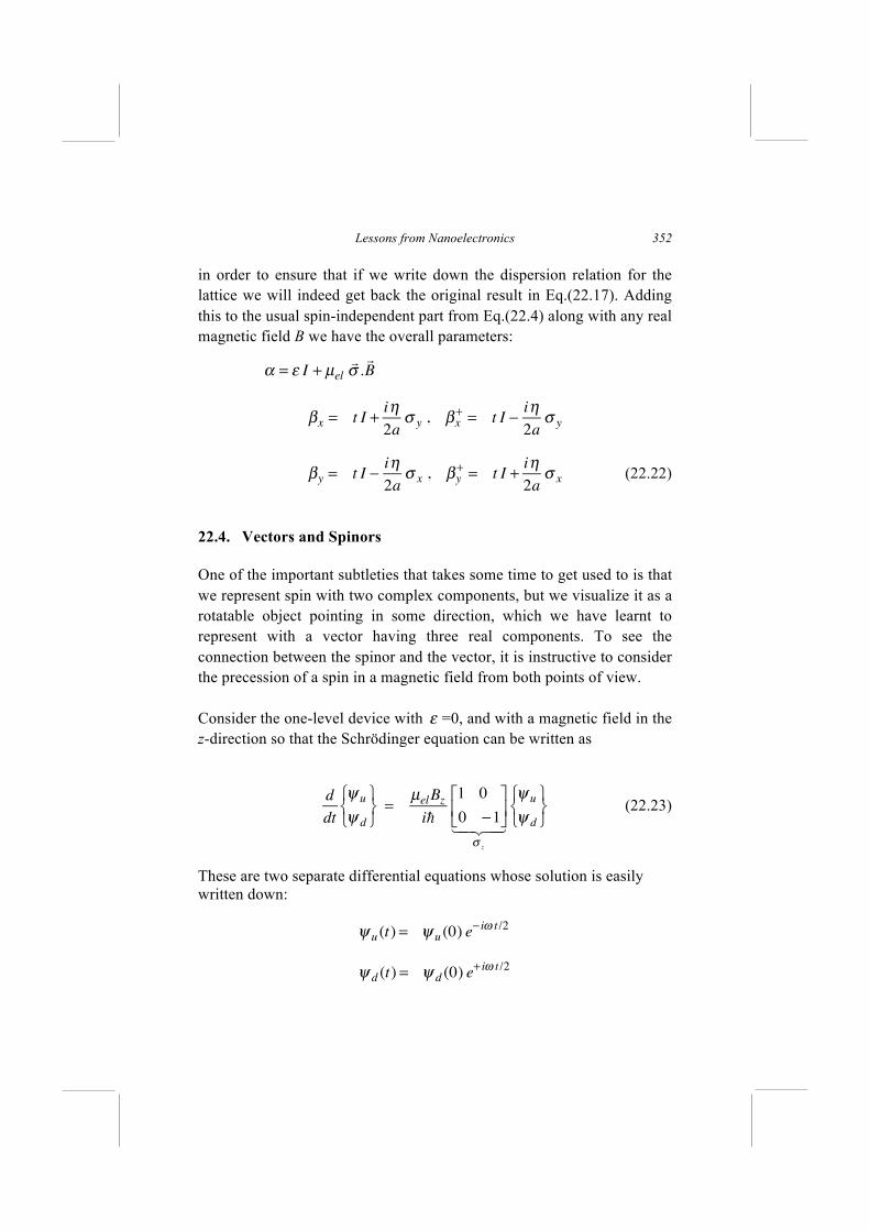
Lessons from Nanoelectronics
352
in order to ensure that if we write down the dispersion relation for the lattice we will indeed get back the original result in Eq.(22.17). Adding this to the usual spin-independent part from Eq.(22.4) along with any real magnetic field B we have the overall parameters:
α = ε I + µel
σ .B
βx = t I +iη
2aσ y , βx
+= t I −
iη
2aσ y
βy = t I −iη
2aσ x , βy
+= t I +
iη
2aσ x (22.22)
22.4. Vectors and Spinors
One of the important subtleties that takes some time to get used to is that we represent spin with two complex components, but we visualize it as a rotatable object pointing in some direction, which we have learnt to represent with a vector having three real components. To see the connection between the spinor and the vector, it is instructive to consider the precession of a spin in a magnetic field from both points of view. Consider the one-level device with ε =0, and with a magnetic field in the z-direction so that the Schrödinger equation can be written as
d
dt
ψ u
ψ d
⎧⎨⎩
⎫⎬⎭=
µelBz
i
1 0
0 −1⎡
⎣⎢
⎤
⎦⎥
σz
ψ u
ψ d
⎧⎨⎩
⎫⎬⎭
(22.23)
These are two separate differential equations whose solution is easily written down:
ψ u (t) = ψ u (0) e− iω t /2
ψ d (t) = ψ d (0) e+ iω t /2
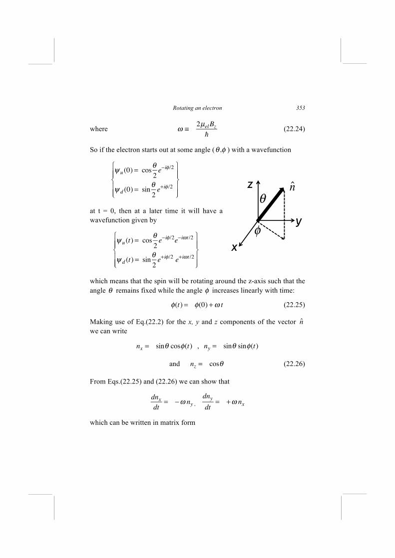
Rotating an electron
353
where
ω ≡2µelBz
(22.24)
So if the electron starts out at some angle (θ ,φ ) with a wavefunction
ψ u (0) = cos
θ2e−iφ /2
ψ d (0) = sinθ2e+iφ /2
⎧
⎨⎪⎪
⎩⎪⎪
⎫
⎬⎪⎪
⎭⎪⎪
at t = 0, then at a later time it will have a wavefunction given by
ψ u (t) = cos
θ2e−iφ /2
e−iωt /2
ψ d (t) = sinθ2e+iφ /2
e+iωt /2
⎧
⎨⎪⎪
⎩⎪⎪
⎫
⎬⎪⎪
⎭⎪⎪
which means that the spin will be rotating around the z-axis such that the angle θ remains fixed while the angle φ increases linearly with time:
φ(t) = φ(0) +ω t (22.25)
Making use of Eq.(22.2) for the x, y and z components of the vector n we can write
nx= sinθ cosφ(t) , ny = sinθ sinφ(t)
and nz = cosθ (22.26)
From Eqs.(22.25) and (22.26) we can show that
dnx
dt= −ω ny ,
dny
dt= +ω nx
which can be written in matrix form
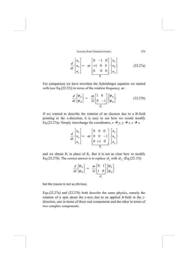
Lessons from Nanoelectronics
354
d
dt
nx
ny
nz
⎧
⎨⎪
⎩⎪
⎫
⎬⎪
⎭⎪= ω
0 −1 0
+1 0 0
0 0 0
⎡
⎣
⎢⎢⎢
⎤
⎦
⎥⎥⎥
Rz
nx
ny
nz
⎧
⎨⎪
⎩⎪
⎫
⎬⎪
⎭⎪
(22.27a)
For comparison we have rewritten the Schrödinger equation we started with (see Eq.(22.23)) in terms of the rotation frequency ω :
d
dt
ψ u
ψ d
⎧⎨⎩
⎫⎬⎭=
ω2i
1 0
0 −1⎡
⎣⎢
⎤
⎦⎥
σz
ψ u
ψ d
⎧⎨⎩
⎫⎬⎭
(22.27b)
If we wanted to describe the rotation of an electron due to a B-field pointing in the x-direction, it is easy to see how we would modify Eq.(22.27a): Simply interchange the coordinates, x y, y z, z x.
d
dt
nx
ny
nz
⎧
⎨⎪
⎩⎪
⎫
⎬⎪
⎭⎪= ω
0 0 0
0 0 −1
0 +1 0
⎡
⎣
⎢⎢⎢
⎤
⎦
⎥⎥⎥
Rx
nx
ny
nz
⎧
⎨⎪
⎩⎪
⎫
⎬⎪
⎭⎪
and we obtain Rx in place of Rz. But it is not as clear how to modify Eq.(22.27b). The correct answer is to replace σ z with σ
x (Eq.(22.15))
d
dt
ψ u
ψ d
⎧⎨⎩
⎫⎬⎭=
ω2i
0 1
1 0
⎡
⎣⎢
⎤
⎦⎥
σx
ψ u
ψ d
⎧⎨⎩
⎫⎬⎭
but the reason is not as obvious. Eqs.(22.27a) and (22.27b) both describe the same physics, namely the rotation of a spin about the z-axis due to an applied B-field in the z-direction, one in terms of three real components and the other in terms of two complex components.
Rotating an electron
355
But what do matrices like R in Eq.(22.27a) have in common with matrices like σ in Eq.(22.27b) that makes them “isomorphic” allowing them to describe the same physics? Answer: They obey the same “commutation relations”. Let me explain.
It is easy to check that the matrices
Rx=
0 0 0
0 0 −1
0 +1 0
⎡
⎣
⎢⎢⎢
⎤
⎦
⎥⎥⎥
, Ry =
0 0 +1
0 0 0
−1 0 0
⎡
⎣
⎢⎢⎢
⎤
⎦
⎥⎥⎥
Rz =
0 −1 0
+1 0 0
0 0 0
⎡
⎣
⎢⎢⎢
⎤
⎦
⎥⎥⎥
obey the relations
RxRy − RyRx = Rz
RyRz − RzRy = Rx (22.28a)
RzRx − RxRz = Ry
The Pauli spin matrices obey a similar relationship with R replaced by σ / 2i :
σ xσ y −σ yσ x = 2iσ z
σ yσ z −σ zσ y = 2iσ x (22.28b)
σ zσ x −σ xσ z = 2iσ y
The standard textbook introduction to spin starts from these commutation relations and argues that they are a property of the “rotation group”. In order to find a mathematical representation with two components for a rotatable object, one must first write down three (2x2) matrices obeying
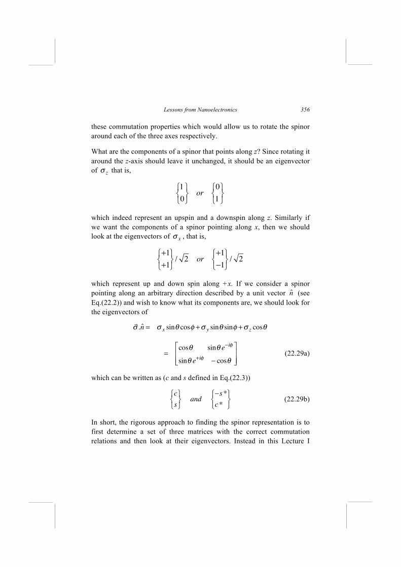
Lessons from Nanoelectronics
356
these commutation properties which would allow us to rotate the spinor around each of the three axes respectively.
What are the components of a spinor that points along z? Since rotating it around the z-axis should leave it unchanged, it should be an eigenvector of σ z that is,
which indeed represent an upspin and a downspin along z. Similarly if we want the components of a spinor pointing along x, then we should look at the eigenvectors of σ
x, that is,
which represent up and down spin along +x. If we consider a spinor pointing along an arbitrary direction described by a unit vector n (see Eq.(22.2)) and wish to know what its components are, we should look for the eigenvectors of
σ .n = σ x sinθ cosφ +σ y sinθ sinφ +σ z cosθ
=cosθ sinθ e−iφ
sinθ e+iφ − cosθ
⎡
⎣⎢⎢
⎤
⎦⎥⎥
(22.29a)
which can be written as (c and s defined in Eq.(22.3))
c
s
⎧⎨⎩
⎫⎬⎭
and−s*
c*
⎧⎨⎩
⎫⎬⎭
(22.29b)
In short, the rigorous approach to finding the spinor representation is to first determine a set of three matrices with the correct commutation relations and then look at their eigenvectors. Instead in this Lecture I
1
0
⎧⎨⎩
⎫⎬⎭
or0
1
⎧⎨⎩
⎫⎬⎭
+1
+1
⎧⎨⎩
⎫⎬⎭/ 2 or
+1
−1
⎧⎨⎩
⎫⎬⎭/ 2
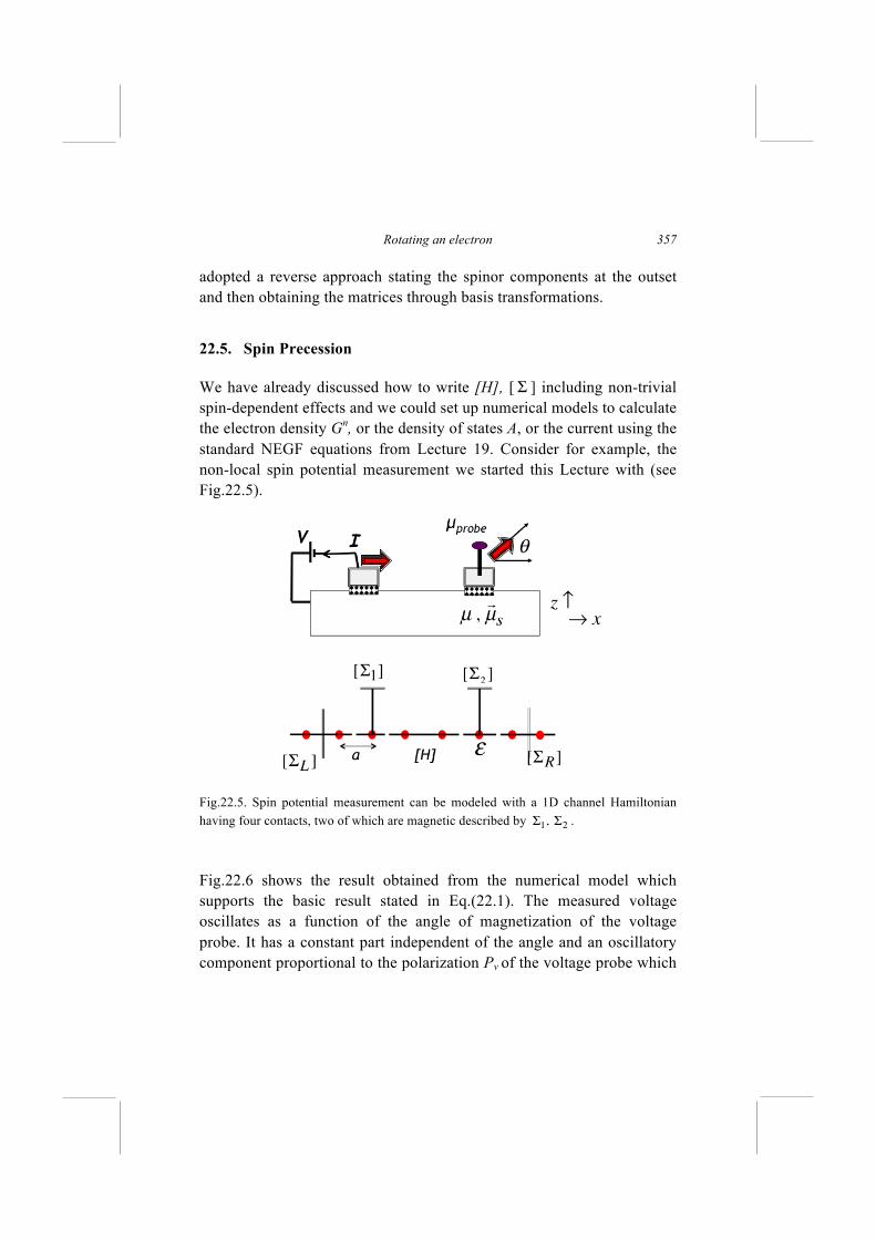
Rotating an electron
357
adopted a reverse approach stating the spinor components at the outset and then obtaining the matrices through basis transformations.
22.5. Spin Precession
We have already discussed how to write [H], [ Σ ] including non-trivial spin-dependent effects and we could set up numerical models to calculate the electron density Gn, or the density of states A, or the current using the standard NEGF equations from Lecture 19. Consider for example, the non-local spin potential measurement we started this Lecture with (see Fig.22.5).
Fig.22.5. Spin potential measurement can be modeled with a 1D channel Hamiltonian having four contacts, two of which are magnetic described by Σ1, Σ2 .
Fig.22.6 shows the result obtained from the numerical model which supports the basic result stated in Eq.(22.1). The measured voltage oscillates as a function of the angle of magnetization of the voltage probe. It has a constant part independent of the angle and an oscillatory component proportional to the polarization Pv of the voltage probe which
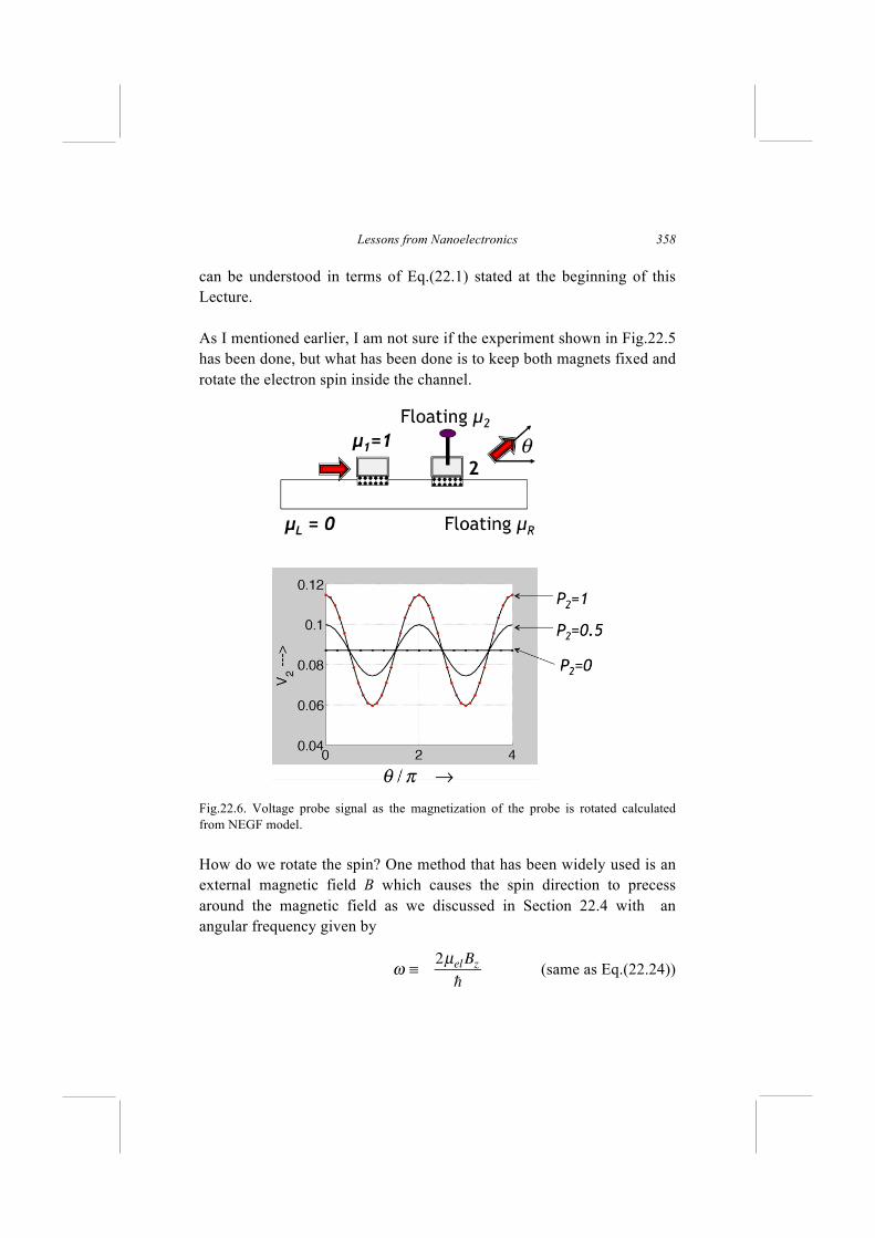
Lessons from Nanoelectronics
358
can be understood in terms of Eq.(22.1) stated at the beginning of this Lecture. As I mentioned earlier, I am not sure if the experiment shown in Fig.22.5 has been done, but what has been done is to keep both magnets fixed and rotate the electron spin inside the channel. Fig.22.6. Voltage probe signal as the magnetization of the probe is rotated calculated from NEGF model. How do we rotate the spin? One method that has been widely used is an external magnetic field B which causes the spin direction to precess around the magnetic field as we discussed in Section 22.4 with an angular frequency given by
ω ≡2µelBz
(same as Eq.(22.24))
Rotating an electron
359
This means that the spin voltage at the point where the probe is connected will rotate by an angle ωτ where τ is the time it takes for the electron to travel from the point of injection to the voltage probe. Writing τ = L/v, we have from Eq.(22.1) using Eq.(22.24)
µprobe = µ + P2µs cos2µelL
νBz (22.31)
One would expect to see an oscillatory signal as a function of the magnetic field. However, one is usually not dealing with ballistic transport, and there is a large spread in the time τ spent by an electron between injection and detection so that the average value of this signal over all τ is essentially zero. What is typically observed is not an oscillatory signal as a function of the B-field but a reduction in the signal from Pµs down to zero, which is referred to as the Hanle signal. However, Hanle signals showing several oscillations have also been observed, but this requires that the spread in τ be much less than its mean value (see for example, Huang et al. 2007). Another possible approach to rotating electron spins is to use the Rashba effect in materials with strong spin-orbit coupling. In many semiconductors, it is now well established that a surface electric field along z (Fig.22.6) leads to an effective magnetic field that depends on the electron momentum. This can be seen by comparing the Hamiltonians for the B-field (Eq.(22.16))
HB = µel
σ .B
with that for the Rashba interaction (22.20) which can be rewritten as
HR = η z . (
σ ×k ) → η
σ . (z ×
k )
suggesting that the effective B-field due to the Rashba interaction is given by
µelBeff = η z ×
k (22.32)
so that from Eq.(22.31) we expect an oscillatory signal of the form
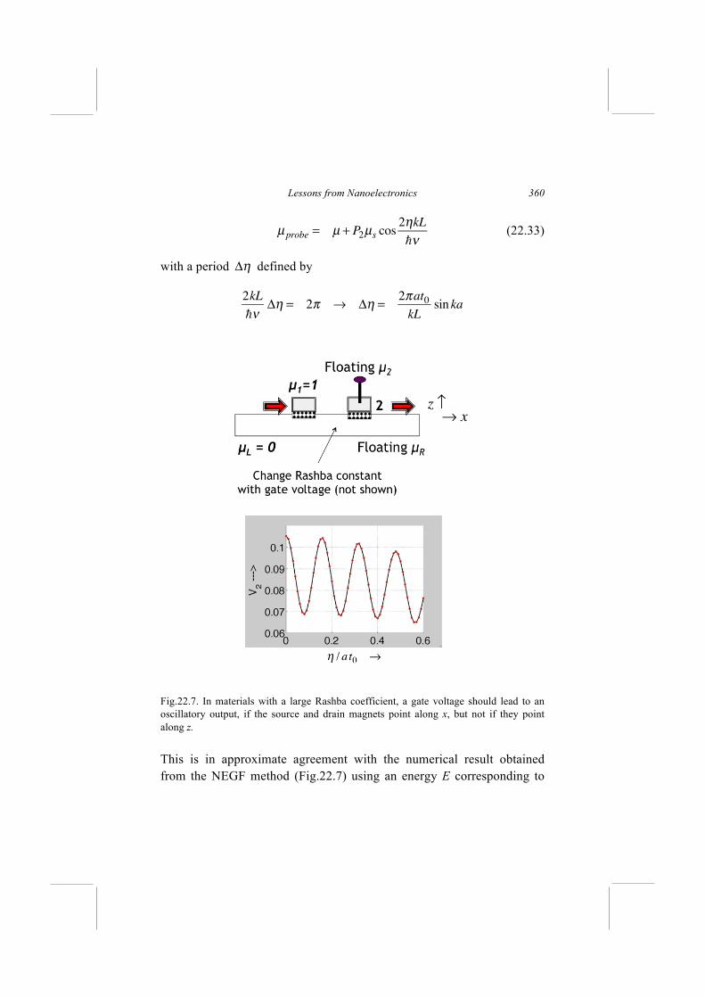
Lessons from Nanoelectronics
360
µprobe = µ + P2µs cos2ηkL
ν (22.33)
with a period Δη defined by
2kL
νΔη = 2π → Δη =
2πat0
kLsin ka
Fig.22.7. In materials with a large Rashba coefficient, a gate voltage should lead to an oscillatory output, if the source and drain magnets point along x, but not if they point along z. This is in approximate agreement with the numerical result obtained from the NEGF method (Fig.22.7) using an energy E corresponding to
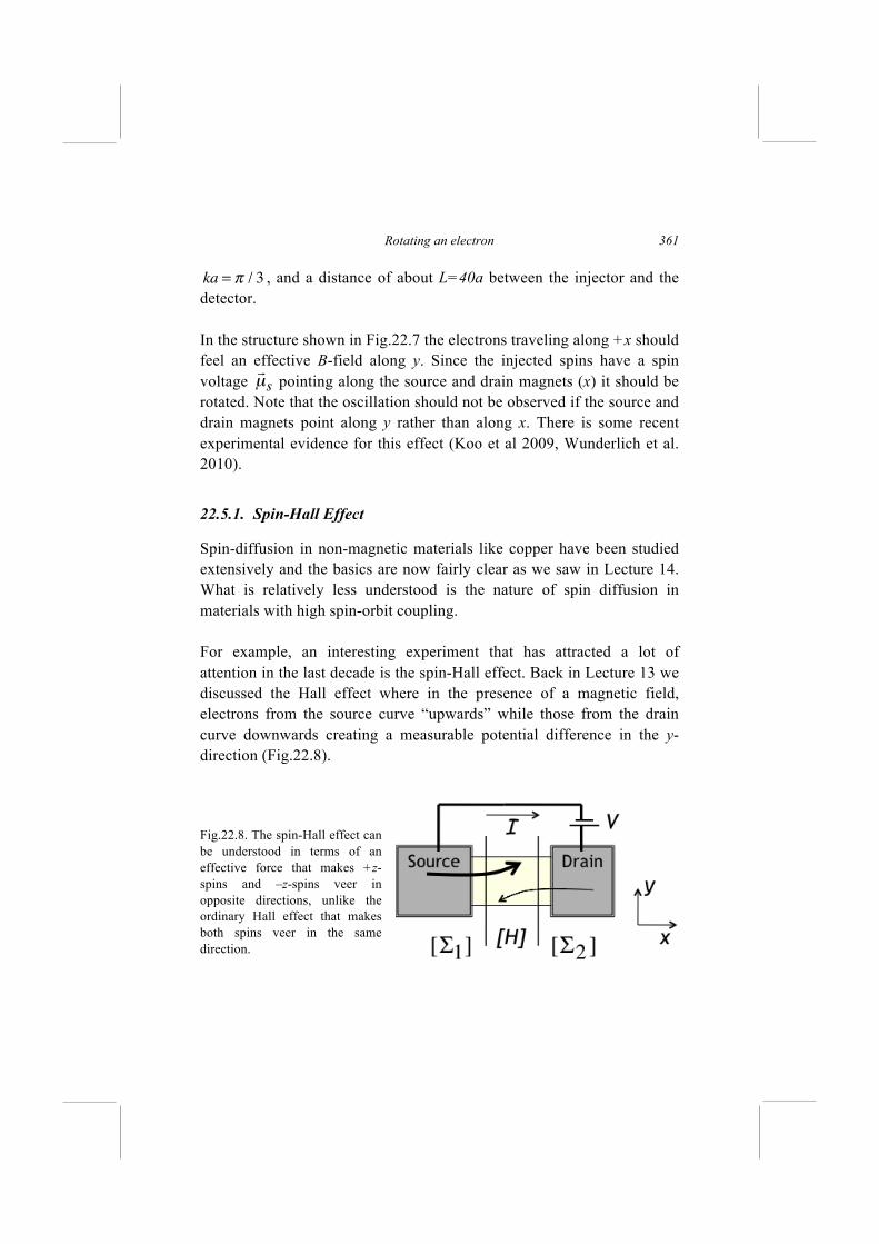
Rotating an electron
361
ka = π / 3 , and a distance of about L=40a between the injector and the detector. In the structure shown in Fig.22.7 the electrons traveling along +x should feel an effective B-field along y. Since the injected spins have a spin voltage pointing along the source and drain magnets (x) it should be rotated. Note that the oscillation should not be observed if the source and drain magnets point along y rather than along x. There is some recent experimental evidence for this effect (Koo et al 2009, Wunderlich et al. 2010).
22.5.1. Spin-Hall Effect
Spin-diffusion in non-magnetic materials like copper have been studied extensively and the basics are now fairly clear as we saw in Lecture 14. What is relatively less understood is the nature of spin diffusion in materials with high spin-orbit coupling. For example, an interesting experiment that has attracted a lot of attention in the last decade is the spin-Hall effect. Back in Lecture 13 we discussed the Hall effect where in the presence of a magnetic field, electrons from the source curve “upwards” while those from the drain curve downwards creating a measurable potential difference in the y-direction (Fig.22.8). Fig.22.8. The spin-Hall effect can be understood in terms of an effective force that makes +z-spins and –z-spins veer in opposite directions, unlike the ordinary Hall effect that makes both spins veer in the same direction.
€
µ s
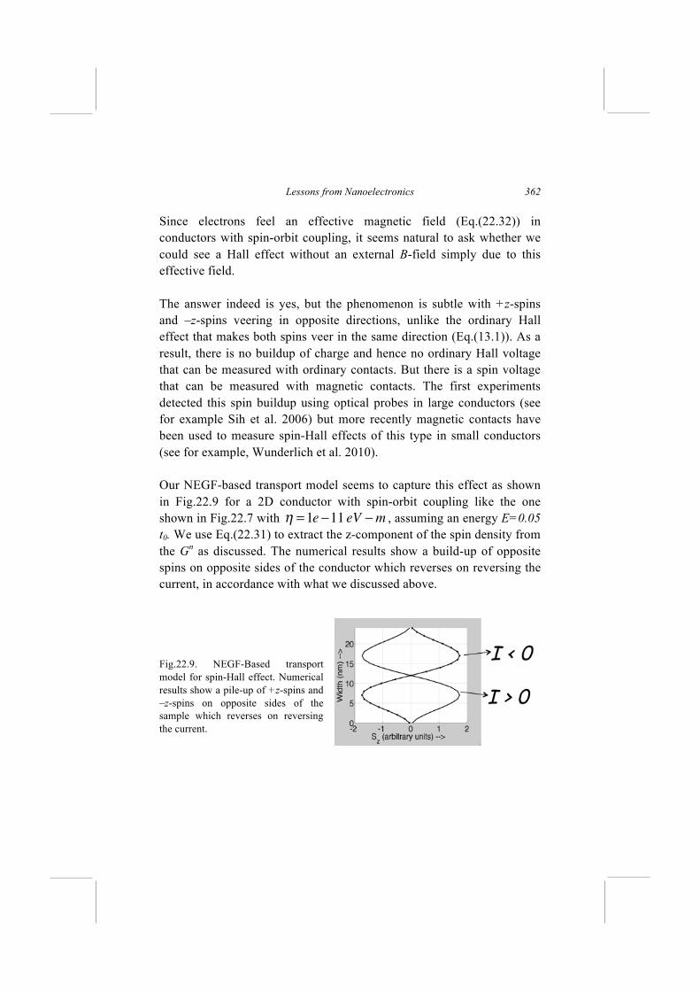
Lessons from Nanoelectronics
362
Since electrons feel an effective magnetic field (Eq.(22.32)) in conductors with spin-orbit coupling, it seems natural to ask whether we could see a Hall effect without an external B-field simply due to this effective field. The answer indeed is yes, but the phenomenon is subtle with +z-spins and –z-spins veering in opposite directions, unlike the ordinary Hall effect that makes both spins veer in the same direction (Eq.(13.1)). As a result, there is no buildup of charge and hence no ordinary Hall voltage that can be measured with ordinary contacts. But there is a spin voltage that can be measured with magnetic contacts. The first experiments detected this spin buildup using optical probes in large conductors (see for example Sih et al. 2006) but more recently magnetic contacts have been used to measure spin-Hall effects of this type in small conductors (see for example, Wunderlich et al. 2010). Our NEGF-based transport model seems to capture this effect as shown in Fig.22.9 for a 2D conductor with spin-orbit coupling like the one shown in Fig.22.7 with η =1e −11 eV −m , assuming an energy E=0.05 t0. We use Eq.(22.31) to extract the z-component of the spin density from the Gn as discussed. The numerical results show a build-up of opposite spins on opposite sides of the conductor which reverses on reversing the current, in accordance with what we discussed above. Fig.22.9. NEGF-Based transport model for spin-Hall effect. Numerical results show a pile-up of +z-spins and –z-spins on opposite sides of the sample which reverses on reversing the current.
Rotating an electron
363
There is much activity currently in this general area of spin transport in materials with strong spin-orbit coupling like the “topological insulators” (see for example Xiu et al. 2011 and references therein) which exhibit a more striking version of the spin Hall effect. The main point I want to make is that many striking non-intuitive results come automatically from the NEGF model, allowing one to explore new physics that we may not yet have understood clearly. However, I should mention that we have not discussed the calculation and interpretation of spin currents which are needed in order to couple the transport problem with the LLG equation describing the magnet dynamics (see Fig.14.10). We will not go into this and simply suggest a few references for interested readers.
22.6. From NEGF to Diffusion
Let me end this Lecture by talking a little about the connection between the diffusion equation approach from Lecture 14 with the NEGF-based approach of this Lecture. We have seen that the NEGF-based numerical examples in Fig.22.6, 7 are well described by Eq.(22.1) which follows heuristically from the discussions in Lecture 14. But the reason for this agreement is not obvious, especially since the formal method is based on two-component complex spinors, while
µs is an old-fashioned three-
component real vector. Earlier we talked about the connection between vector n along which a spin points and the wavefunction ψ representing it. To relate Eq.(22.1) to the NEGF method we need to consider quantities like Gn
~ ψψ + rather than the wavefunction ψ , since the NEGF is formulated in terms of Gn. Besides it is Gn and not ψ that is observable and can be related to experiment.
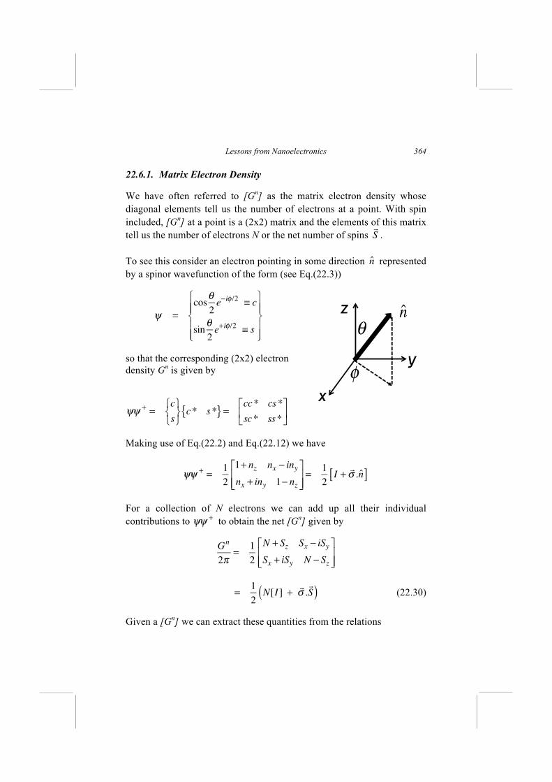
Lessons from Nanoelectronics
364
22.6.1. Matrix Electron Density
We have often referred to [Gn] as the matrix electron density whose diagonal elements tell us the number of electrons at a point. With spin included, [Gn] at a point is a (2x2) matrix and the elements of this matrix tell us the number of electrons N or the net number of spins
S .
To see this consider an electron pointing in some direction n represented by a spinor wavefunction of the form (see Eq.(22.3))
ψ =
cosθ2e−iφ /2 ≡ c
sinθ2e+iφ /2 ≡ s
⎧
⎨⎪⎪
⎩⎪⎪
⎫
⎬⎪⎪
⎭⎪⎪
so that the corresponding (2x2) electron density Gn is given by
ψψ +=
c
s
⎧⎨⎩
⎫⎬⎭c* s*{ } =
cc* cs*
sc* ss*
⎡
⎣⎢
⎤
⎦⎥
Making use of Eq.(22.2) and Eq.(22.12) we have
ψψ +=
1
2
1+ nz nx − inynx + iny 1− nz
⎡
⎣⎢⎢
⎤
⎦⎥⎥=
1
2I +σ .n[ ]
For a collection of N electrons we can add up all their individual contributions to ψψ + to obtain the net [Gn] given by
Gn
2π=
1
2
N + Sz Sx − iSy
Sx + iSy N − Sz
⎡
⎣⎢⎢
⎤
⎦⎥⎥
=1
2N[I ] +
σ .S( ) (22.30)
Given a [Gn] we can extract these quantities from the relations
Rotating an electron
365
N =1
2πTrace[G
n] ,
S =
1
2πTrace[
σ G
n] (22.31)
which follow from Eq.(22.30) if we make use of the fact that all three matrices (Eq.(22.15)) have zero trace, along with the following properties of the Pauli spin matrices that are easily verified.
σ x2=σ y
2=σ z
2= I (22.32a)
σ xσ y = − σ yσ x = iσ z (22.32b)
σ yσ z = − σ zσ y = iσ x (22.32c)
σ zσ x = − σ xσ z = iσ y (22.32d)
along with the that is the sum of their diagonal elements is zero.
In summary, all the information contained in the 2x2 Hermitian matrix [Gn] can be expressed in terms of four real quantities consisting of a scalar N and the three components of a vector
S which can be extracted
using Eq.(22.31).
22.6.2. Measuring the Spin Potential
That brings us to the question of relating the result stated at the beginning of this Lecture
µprobe = µ +
P.µs
2 (Same as Eq.(22.1))
to the NEGF method. The scalar version of this result was obtained in Lecture 14 (see Eq.(14.23)) using the semiclassical model for a probe shown and setting the probe current to zero. Now we can obtain the general vector version by starting from the NEGF model for a probe (Fig22.10) with the current given by (see Eq.(19.4))
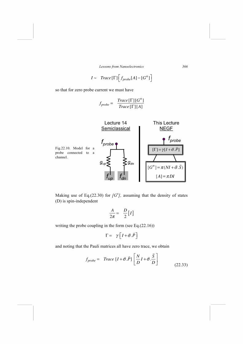
Lessons from Nanoelectronics
366
I ~ Trace [Γ] fprobe[A] − [Gn]⎡
⎣⎤⎦
so that for zero probe current we must have
fprobe =Trace [Γ] [G
n]
Trace [Γ] [A]
Fig.22.10. Model for a probe connected to a channel.
Making use of Eq.(22.30) for [Gn], assuming that the density of states (D) is spin-independent
A
2π=
D
2I[ ]
writing the probe coupling in the form (see Eq.(22.16))
Γ = γ I +
σ .P⎡⎣ ⎤⎦
and noting that the Pauli matrices all have zero trace, we obtain
fprobe = Trace [I +σ .P]
N
DI +σ .
S
D
⎡
⎣⎢
⎤
⎦⎥
(22.33)
Rotating an electron
367
Once again there is an identity that can be used to simplify this expression: For any two vectors
P and
B , it is straightforward (but
takes some algebra) to verify that
[σ .P] [σ .B] = (
P.B)[I ] + i
σ .[P ×B] , so that
[I +σ .P] b I +
σ .B⎡⎣ ⎤⎦ = (b +
P.B)[I ] +
σ .[P +B + iP ×B] (22.34)
Making use of this identity and noting once again that the Pauli matrices have zero trace, we can write from Eq.(12.33)
fprobe =N
D+P.
S
D≡ f +
P.
fs
2 (22.35)
where the charge occupation f and the spin occupation fs are each defined such that their maximum possible values are one. We can translate this relation in terms of occupation into the relation in terms of potentials stated earlier (see Eq.(22.1)) using the linear relation between the two for small bias (see Eq.(2.8)).
22.6.3. Four-Component Diffusion
The key point we want to stress is that the quantum formalism naturally leads to a 2x2 complex matrix [Gn] at each point, but it is straightforward to translate it into four physically transparent components, like N,
S or
µ,
µs .
Back in Lecture 14, we saw how many spin transport phenomena can be understood in terms of the Valet-Fert equation along with a model for the spin-dependent interface resistances. However, this approach is limited to problems that involve spins in one direction (the z-direction) only. Now we have the full NEGF model that can be used for spins pointing in any direction, but it is computationally more demanding and seems conceptually unrelated to the old approach. By translating the information in [Gn] into N,
S we can bridge this gap. For example, the
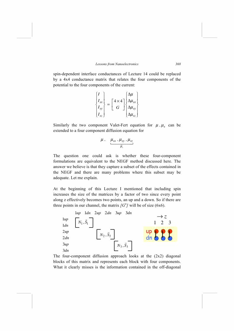
Lessons from Nanoelectronics
368
spin-dependent interface conductances of Lecture 14 could be replaced by a 4x4 conductance matrix that relates the four components of the potential to the four components of the current:
I
Isx
Isy
Isz
⎧
⎨
⎪⎪
⎩
⎪⎪
⎫
⎬
⎪⎪
⎭
⎪⎪
=4 × 4
G
⎡
⎣⎢
⎤
⎦⎥
Δµ
ΔµsxΔµsy
Δµsz
⎧
⎨
⎪⎪
⎩
⎪⎪
⎫
⎬
⎪⎪
⎭
⎪⎪
Similarly the two component Valet-Fert equation for µ , µs can be extended to a four component diffusion equation for
µ , µsx , µsy , µszµs
The question one could ask is whether these four-component formulations are equivalent to the NEGF method discussed here. The answer we believe is that they capture a subset of the effects contained in the NEGF and there are many problems where this subset may be adequate. Let me explain. At the beginning of this Lecture I mentioned that including spin increases the size of the matrices by a factor of two since every point along z effectively becomes two points, an up and a down. So if there are three points in our channel, the matrix [Gn] will be of size (6x6).
The four-component diffusion approach looks at the (2x2) diagonal blocks of this matrix and represents each block with four components. What it clearly misses is the information contained in the off-diagonal
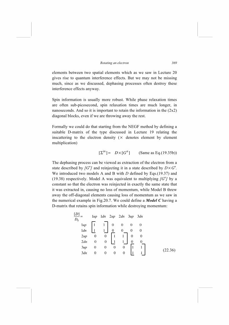
Rotating an electron
369
elements between two spatial elements which as we saw in Lecture 20 gives rise to quantum interference effects. But we may not be missing much, since as we discussed, dephasing processes often destroy these interference effects anyway. Spin information is usually more robust. While phase relaxation times are often sub-picosecond, spin relaxation times are much longer, in nanoseconds. And so it is important to retain the information in the (2x2) diagonal blocks, even if we are throwing away the rest. Formally we could do that starting from the NEGF method by defining a suitable D-matrix of the type discussed in Lecture 19 relating the inscattering to the electron density (× denotes element by element multiplication)
[Σin] = D × [G
n] (Same as Eq.(19.35b))
The dephasing process can be viewed as extraction of the electron from a state described by [Gn] and reinjecting it in a state described by D × Gn. We introduced two models A and B with D defined by Eqs.(19.37) and (19.38) respectively. Model A was equivalent to multiplying [Gn] by a constant so that the electron was reinjected in exactly the same state that it was extracted in, causing no loss of momentum, while Model B threw away the off-diagonal elements causing loss of momentum as we saw in the numerical example in Fig.20.7. We could define a Model C having a D-matrix that retains spin information while destroying momentum:
(22.36)
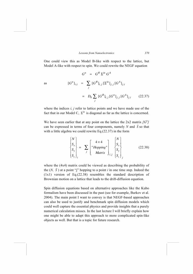
Lessons from Nanoelectronics
370
One could view this as Model B-like with respect to the lattice, but Model A-like with respect to spin. We could rewrite the NEGF equation
Gn
= GRΣinGA
as [Gn] i,i =
j
∑ [GR]i, j [Σ
in] j, j [G
A] j,i
= D0j
∑ [GR]i, j [G
n] j, j [G
A] j,i (22.37)
where the indices i, j refer to lattice points and we have made use of the fact that in our Model C, Σin is diagonal as far as the lattice is concerned. We have seen earlier that at any point on the lattice the 2x2 matrix [Gn] can be expressed in terms of four components, namely N and
S so that
with a little algebra we could rewrite Eq.(22.37) in the form
N
Sx
Sy
Sz
⎧
⎨
⎪⎪
⎩
⎪⎪
⎫
⎬
⎪⎪
⎭
⎪⎪i
=
j
∑4 × 4
"Hopping"
Matrix
⎡
⎣
⎢⎢⎢
⎤
⎦
⎥⎥⎥i, j
N
Sx
Sy
Sz
⎧
⎨
⎪⎪
⎩
⎪⎪
⎫
⎬
⎪⎪
⎭
⎪⎪j
(22.38)
where the (4x4) matrix could be viewed as describing the probability of the (N,
S ) at a point “j” hopping to a point i in one time step. Indeed the
(1x1) version of Eq.(22.38) resembles the standard description of Brownian motion on a lattice that leads to the drift-diffusion equation. Spin diffusion equations based on alternative approaches like the Kubo formalism have been discussed in the past (see for example, Burkov et al. 2004). The main point I want to convey is that NEGF-based approaches can also be used to justify and benchmark spin diffusion models which could well capture the essential physics and provide insights that a purely numerical calculation misses. In the last lecture I will briefly explain how one might be able to adapt this approach to more complicated spin-like objects as well. But that is a topic for future research.
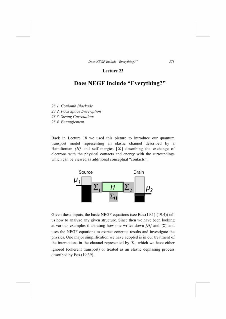
Does NEGF Include “Everything?”
371
Lecture 23
Does NEGF Include “Everything?”
23.1. Coulomb Blockade 23.2. Fock Space Description 23.3. Strong Correlations 23.4. Entanglement Back in Lecture 18 we used this picture to introduce our quantum transport model representing an elastic channel described by a Hamiltonian [H] and self-energies [ Σ ] describing the exchange of electrons with the physical contacts and energy with the surroundings which can be viewed as additional conceptual “contacts”.
Given these inputs, the basic NEGF equations (see Eqs.(19.1)-(19.4)) tell us how to analyze any given structure. Since then we have been looking at various examples illustrating how one writes down [H] and [Σ] and uses the NEGF equations to extract concrete results and investigate the physics. One major simplification we have adopted is in our treatment of the interactions in the channel represented by Σ0 which we have either ignored (coherent transport) or treated as an elastic dephasing process described by Eqs.(19.39).
Lessons from Nanoelectronics
372
This choice of self-energy functions leads to no exchange of energy with the surroundings, but it has an effect on transport due to the exchange of momentum and “phase”. Basically we have been talking about elastic resistors like the ones we started these Lectures with, except that we are now including quantum mechanical effects. One could say that in the last few Lectures we have applied the general Non-Equilibrium Green’s Function (NEGF) method to an elastic resistor, just as in Part one we applied the general Boltzmann Transport Equation (BTE) to an elastic resistor.
So how do we go beyond elastic resistors? For semiclassical transport, it is clear in principle how to include different types of interaction into the BTE for realistic devices and much progress has been made in this direction. Similarly for quantum transport, the NEGF tells us how to evaluate the self-energy Σ0 for any given microscopic interaction. In these lectures we have talked only about elastic dephasing which is a small subset of the interactions considered in the classic work on NEGF (see for example, Danielewicz 1984 or Mahan 1987). In practice, however, it remains numerically challenging to go beyond elastic resistors and approximate methods continue to be used widely. Readers interested in the details of device analysis at high bias may find an old article (Datta (2000)) useful. This article has a number of concrete results obtained using MATLAB codes that I had offered to share with anyone who asked me for it. Over the years many have requested these codes from me which makes me think they may be somewhat useful and we plan to have these available on our website for these notes. I should mention that many devices are rather forgiving when it comes to modeling the physics of ineastic scattering correctly. Devices with energy levels that are equally connected to both contacts (Fig.9.5b.) do not really test the deep physics of inelastic transport and cannot distinguish between a good theory and a bad one. A good test for inelastic scattering models is the device shown in Fig.9.5a for which the entire terminal current is driven by inelastic processes. Only a
Does NEGF Include “Everything?”
373
fundamentally sound theory will predict results that comply with the requirements of the second law. But practical issues apart, can the NEGF method model “everything”, at least in principle? The formal NEGF method developed in the 1960’s was based on many-body perturbation theory (MBPT) which provided clear prescriptions for evaluating the self-energy functions
Σ , Σin for a given microscopic interaction up to any order in perturbation theory. It may seem that using MBPT we can in principle include everything. However, I believe this is not quite true since it is basically a perturbation theory which in a broad sense amounts to evaluating a quantity like (1-x)-1 by summing a series like 1+x+x2+x3+ …. , which works very well if x is much less than one. But if x happens to exceed one, it does not work and one needs non-perturbative methods, or perhaps a different perturbation parameter. This is one of the reasons I prefer to decouple the NEGF equations (Eqs.(19.1) through (19.4)) from the MBPT-based methods used to evaluate the self-energy functions. The latter may well evolve and get supplemented as people find better approximations that capture the physics in specific situations. With equilibrium problems, for example, density functional theory (DFT)-based techniques have proven to be very successful and are often used in quantum chemistry in place of MBPT. I believe one should be cautious about expecting the same success with non-equilibrium problems where a far greater spectrum of many body states are made accessible and can be manipulated through a judicious choice of contacts, but it is quite likely that people will find insightful approaches that capture the essential physics in specific problems.
Lessons from Nanoelectronics
374
Like the BTE for semiclassical transport, NEGF-based methods in their simplest form, seem to provide a good description of problems where electron-electron interactions can be treated within a mean field theory based on the widely used picture of quasi-independent electrons moving in a self-consistent potential U due to the other electrons (Section 18.2). As we saw in Lecture 8, for low bias calculations one needs to consider only the equilibrium potential which is already included in the semi-empirical tight-binding (TB) parameters used to construct our Hamiltonian [H]. For real devices operating at high bias, the change in the potential due to any changes in the electron occupation in the channel are routinely included using the Poisson equation which is the simplest approximation to the very difficult problem of electron-electron interactions and there have been extensive discussions of how the self-consistent field (scf) can be corrected to obtain better agreement with experimental results. However, there are examples where the self-consistent field approach itself seems to fail and some of the most intriguing properties arise from a failure of this simple picture. The purpose of this Lecture is to alert the reader that a straightforward application of NEGF may well miss these important experimentally observable effects. Future challenges and opportunities may well involve effects of this type, requiring insightful choices for Σ , Σin if we wish to use the NEGF method.
23.1. Coulomb Blockade
In the spirit of the bottom-up approach let us consider the simplest resistor that will show this effect, one that is only slightly more complicated than the one-level resistor we started with (Fig.3.1). We assume two levels, a spin up and a spin down, having the same energy , with the equilibrium chemical potential µ located right at , so that each level is half-filled since the Fermi function f0(E=µ) equals 0.5. Based on what we have discussed so far we would expect a high conductance since €
ε
€
ε
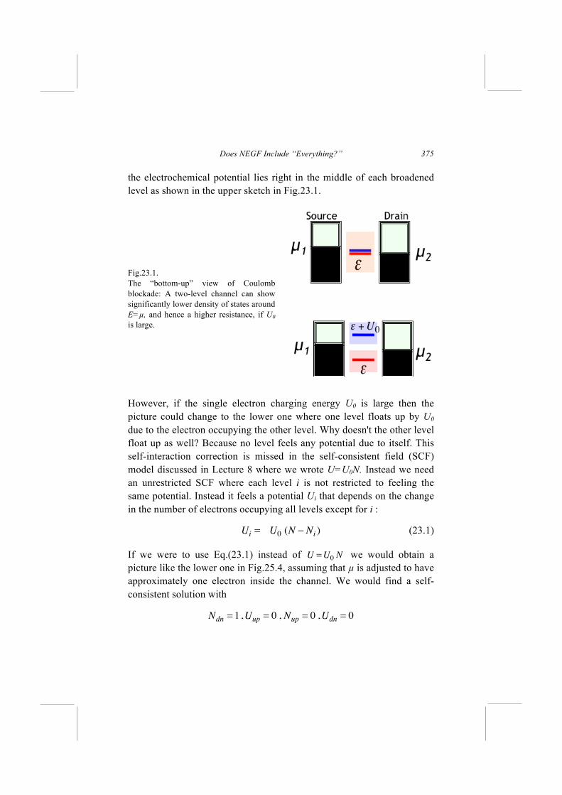
Does NEGF Include “Everything?”
375
the electrochemical potential lies right in the middle of each broadened level as shown in the upper sketch in Fig.23.1. Fig.23.1. The “bottom-up” view of Coulomb blockade: A two-level channel can show significantly lower density of states around E=µ, and hence a higher resistance, if U0 is large. However, if the single electron charging energy U0 is large then the picture could change to the lower one where one level floats up by U0 due to the electron occupying the other level. Why doesn't the other level float up as well? Because no level feels any potential due to itself. This self-interaction correction is missed in the self-consistent field (SCF) model discussed in Lecture 8 where we wrote U=U0N. Instead we need an unrestricted SCF where each level i is not restricted to feeling the same potential. Instead it feels a potential Ui that depends on the change in the number of electrons occupying all levels except for i :
Ui = U0 (N − Ni ) (23.1)
If we were to use Eq.(23.1) instead of U =U0 N we would obtain a picture like the lower one in Fig.25.4, assuming that µ is adjusted to have approximately one electron inside the channel. We would find a self-consistent solution with
Ndn = 1,Uup = 0 , Nup = 0 ,Udn = 0
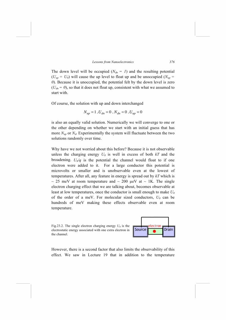
Lessons from Nanoelectronics
376
The down level will be occupied (Ndn = 1) and the resulting potential (Uup = U0) will cause the up level to float up and be unoccupied (Nup = 0). Because it is unoccupied, the potential felt by the down level is zero (Udn = 0), so that it does not float up, consistent with what we assumed to start with. Of course, the solution with up and down interchanged
Nup = 1,Udn = 0 , Ndn = 0 ,Uup = 0
is also an equally valid solution. Numerically we will converge to one or the other depending on whether we start with an initial guess that has more Nup or Nd. Experimentally the system will fluctuate between the two solutions randomly over time. Why have we not worried about this before? Because it is not observable unless the charging energy U0 is well in excess of both kT and the broadening. U0/q is the potential the channel would float to if one electron were added to it. For a large conductor this potential is microvolts or smaller and is unobservable even at the lowest of temperatures. After all, any feature in energy is spread out by kT which is ~ 25 meV at room temperature and ~ 200 µeV at ~ 1K. The single electron charging effect that we are talking about, becomes observable at least at low temperatures, once the conductor is small enough to make U0 of the order of a meV. For molecular sized conductors, U0 can be hundreds of meV making these effects observable even at room temperature. Fig.23.2. The single electron charging energy U0 is the electrostatic energy associated with one extra electron in the channel. However, there is a second factor that also limits the observability of this effect. We saw in Lecture 19 that in addition to the temperature
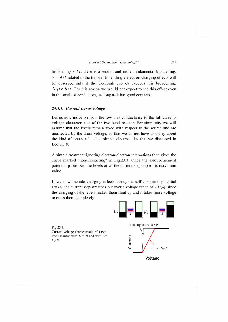
Does NEGF Include “Everything?”
377
broadening ~ kT, there is a second and more fundamental broadening, related to the transfer time. Single electron charging effects will
be observed only if the Coulomb gap U0 exceeds this broadening: . For this reason we would not expect to see this effect even
in the smallest conductors, as long as it has good contacts.
24.1.1. Current versus voltage
Let us now move on from the low bias conductance to the full current-voltage characteristics of the two-level resistor. For simplicity we will assume that the levels remain fixed with respect to the source and are unaffected by the drain voltage, so that we do not have to worry about the kind of issues related to simple electrostatics that we discussed in Lecture 8. A simple treatment ignoring electron-electron interactions then gives the curve marked "non-interacting" in Fig.23.3. Once the electrochemical potential µ2 crosses the levels at , the current steps up to its maximum value. If we now include charging effects through a self-consistent potential U=U0, the current step stretches out over a voltage range of ~ U0/q, since the charging of the levels makes them float up and it takes more voltage to cross them completely. Fig.23.3. Current-voltage characteristic of a two-level resistor with U = 0 and with U= U0 N
€
γ ~ h / t
€
U0 >> h / t
€
ε
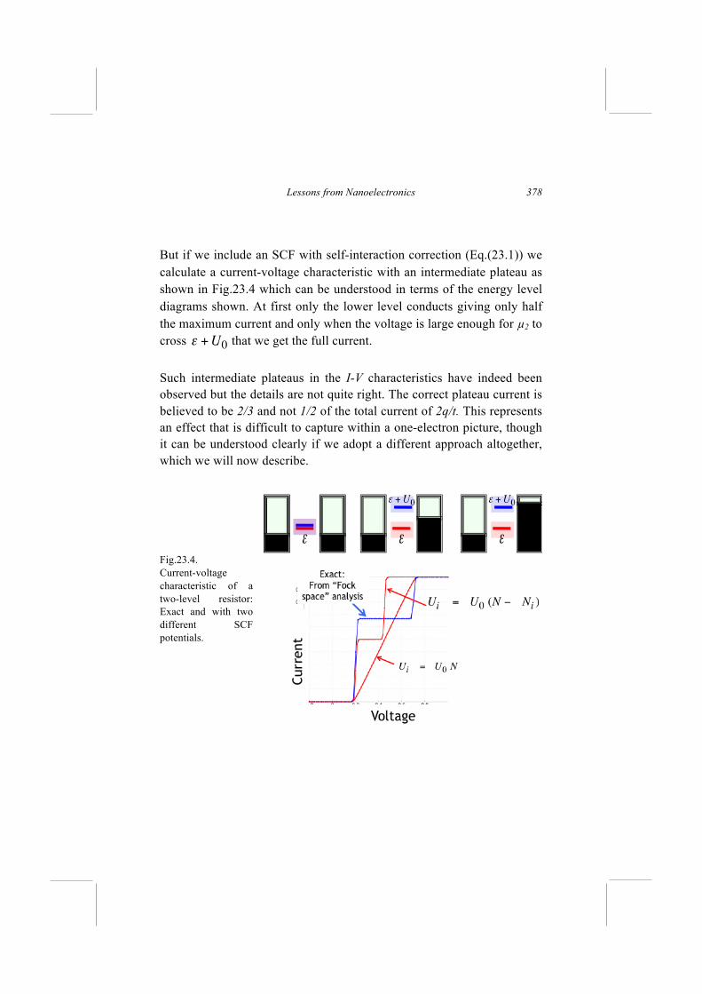
Lessons from Nanoelectronics
378
But if we include an SCF with self-interaction correction (Eq.(23.1)) we calculate a current-voltage characteristic with an intermediate plateau as shown in Fig.23.4 which can be understood in terms of the energy level diagrams shown. At first only the lower level conducts giving only half the maximum current and only when the voltage is large enough for µ2 to cross that we get the full current. Such intermediate plateaus in the I-V characteristics have indeed been observed but the details are not quite right. The correct plateau current is believed to be 2/3 and not 1/2 of the total current of 2q/t. This represents an effect that is difficult to capture within a one-electron picture, though it can be understood clearly if we adopt a different approach altogether, which we will now describe. Fig.23.4. Current-voltage characteristic of a two-level resistor: Exact and with two different SCF potentials.
€
ε +U0
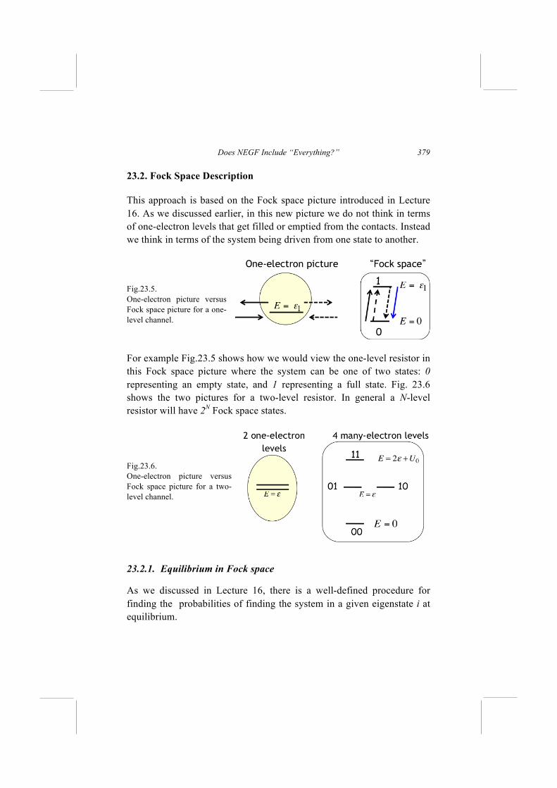
Does NEGF Include “Everything?”
379
23.2. Fock Space Description
This approach is based on the Fock space picture introduced in Lecture 16. As we discussed earlier, in this new picture we do not think in terms of one-electron levels that get filled or emptied from the contacts. Instead we think in terms of the system being driven from one state to another.
Fig.23.5. One-electron picture versus Fock space picture for a one-level channel. For example Fig.23.5 shows how we would view the one-level resistor in this Fock space picture where the system can be one of two states: 0 representing an empty state, and 1 representing a full state. Fig. 23.6 shows the two pictures for a two-level resistor. In general a N-level resistor will have 2N Fock space states. Fig.23.6. One-electron picture versus Fock space picture for a two-level channel.
23.2.1. Equilibrium in Fock space
As we discussed in Lecture 16, there is a well-defined procedure for finding the probabilities of finding the system in a given eigenstate i at equilibrium.
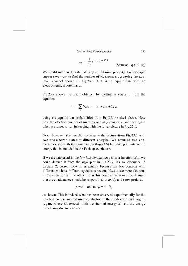
Lessons from Nanoelectronics
380
pi =
1
Ze−(E
i−µN
i)/kT
(Same as Eq.(16.14))
We could use this to calculate any equilibrium property. For example suppose we want to find the number of electrons, n occupying the two-level channel shown in Fig.23.6 if it is in equilibrium with an electrochemical potential µ. Fig.23.7 shows the result obtained by plotting n versus µ from the equation
n = Nii
∑ pi = p01 + p10 + 2p11
using the equilibrium probabilities from Eq.(16.14) cited above. Note how the electron number changes by one as µ crosses ε and then again when µ crosses ε +U0 in keeping with the lower picture in Fig.23.1. Note, however, that we did not assume the picture from Fig.23.1 with two one-electron states at different energies. We assumed two one-electron states with the same energy (Fig.23.6) but having an interaction energy that is included in the Fock space picture. If we are interested in the low bias conductance G as a function of µ, we could deduce it from the n(µ) plot in Fig.23.7. As we discussed in Lecture 2, current flow is essentially because the two contacts with different µ’s have different agendas, since one likes to see more electrons in the channel than the other. From this point of view one could argue that the conductance should be proportional to dn/dµ and show peaks at
µ = ε and at µ = ε +U0
as shown. This is indeed what has been observed experimentally for the low bias conductance of small conductors in the single-electron charging regime where U0 exceeds both the thermal energy kT and the energy broadening due to contacts.
Does NEGF Include “Everything?”
381
Fig.23.7. Equilibrium number of electrons, n in the two-level channel shown in Fig.23.6 as a function of µ, assuming ε = 10kT , U0 = 20kT . The conductance can be argued to be proportional to the derivative dn/dµ showing peaks when µ equals ε and ε +U0 . As we saw in Lecture 15, low bias conductance is an equilibrium property that can be deduced using the principles of equilibrium statistical mechanics. Current flow at higher voltages on the other hand requires the methods of non-equilibrium statistical mechanics. Let me explain briefly how one could understand the 2/3 plateau shown in Fig.23.4 by calculating the current at high bias in the Fock space picture.
23.2.2. Current in the Fock space picture
To calculate the current we write an equation for the probability that the system will be found in one of its available states, which must all add up to one. For example for the one level resistor we could write
ν1p0 = ν2p1 →p1
p0=ν1
ν2
→ p1 =ν1
ν1 +ν2
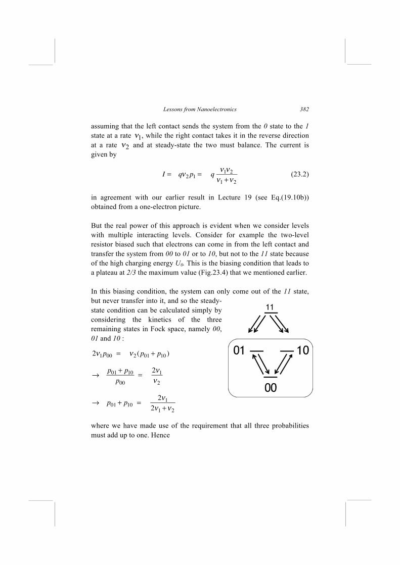
Lessons from Nanoelectronics
382
assuming that the left contact sends the system from the 0 state to the 1 state at a rate , while the right contact takes it in the reverse direction at a rate and at steady-state the two must balance. The current is given by
I = qν2p1 = qν1ν2
ν1 +ν2
(23.2)
in agreement with our earlier result in Lecture 19 (see Eq.(19.10b)) obtained from a one-electron picture. But the real power of this approach is evident when we consider levels with multiple interacting levels. Consider for example the two-level resistor biased such that electrons can come in from the left contact and transfer the system from 00 to 01 or to 10, but not to the 11 state because of the high charging energy U0. This is the biasing condition that leads to a plateau at 2/3 the maximum value (Fig.23.4) that we mentioned earlier. In this biasing condition, the system can only come out of the 11 state, but never transfer into it, and so the steady-state condition can be calculated simply by considering the kinetics of the three remaining states in Fock space, namely 00, 01 and 10 :
2ν1p00 = ν2(p01 + p10 )
→p01 + p10
p00=
2ν1
ν2
→ p01 + p10 =2ν1
2ν1 +ν2
where we have made use of the requirement that all three probabilities must add up to one. Hence
€
ν1
€
ν2
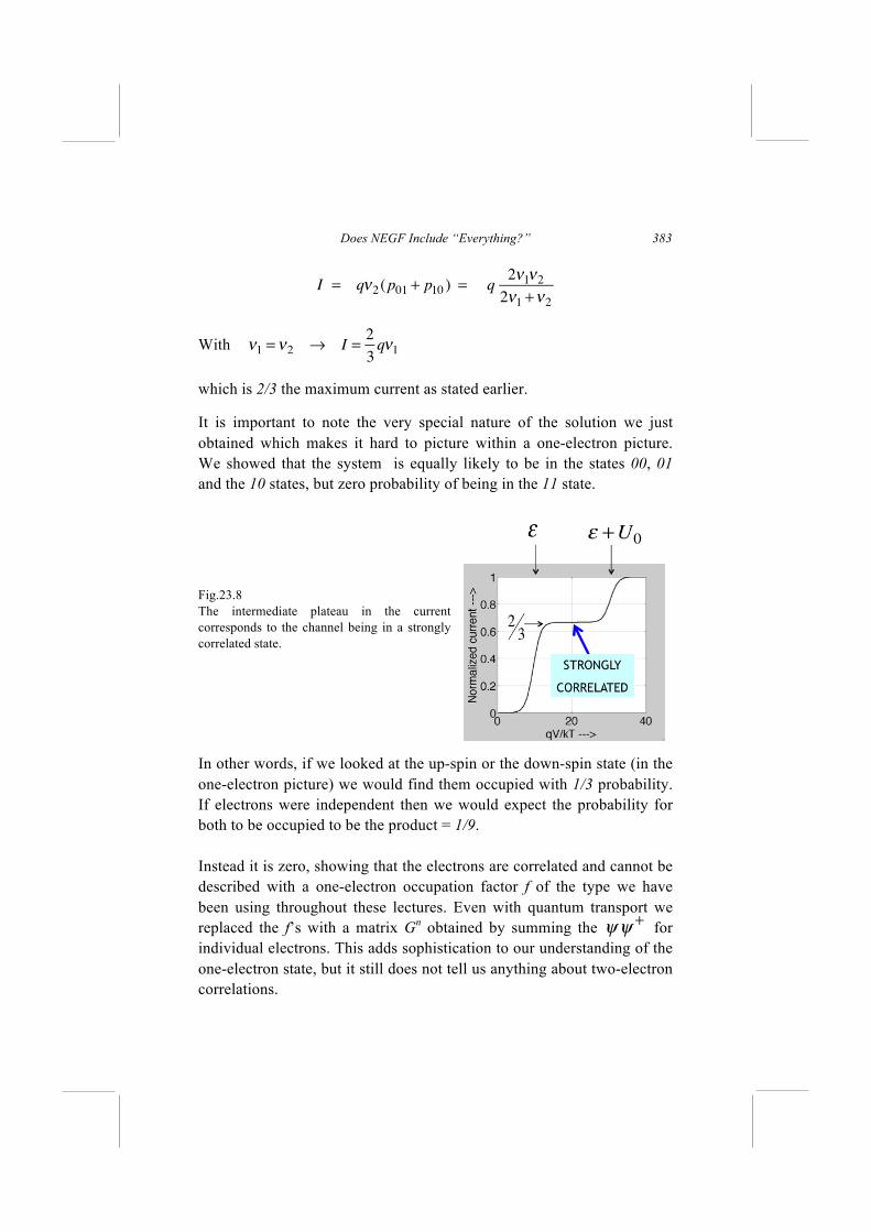
Does NEGF Include “Everything?”
383
I = qν2(p01 + p10 ) = q2ν1ν2
2ν1 +ν2
With ν1 = ν2 → I =2
3qν1
which is 2/3 the maximum current as stated earlier.
It is important to note the very special nature of the solution we just obtained which makes it hard to picture within a one-electron picture. We showed that the system is equally likely to be in the states 00, 01 and the 10 states, but zero probability of being in the 11 state. Fig.23.8 The intermediate plateau in the current corresponds to the channel being in a strongly correlated state. In other words, if we looked at the up-spin or the down-spin state (in the one-electron picture) we would find them occupied with 1/3 probability. If electrons were independent then we would expect the probability for both to be occupied to be the product = 1/9. Instead it is zero, showing that the electrons are correlated and cannot be described with a one-electron occupation factor f of the type we have been using throughout these lectures. Even with quantum transport we replaced the f’s with a matrix Gn obtained by summing the ψψ + for individual electrons. This adds sophistication to our understanding of the one-electron state, but it still does not tell us anything about two-electron correlations.
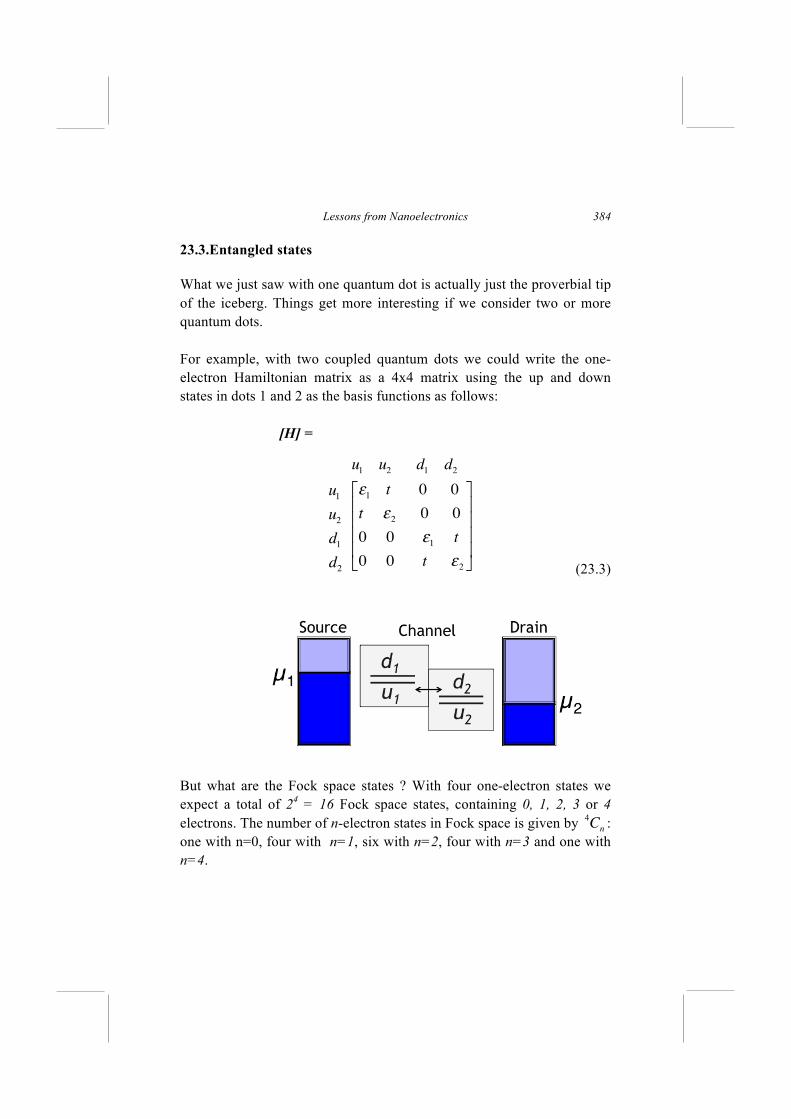
Lessons from Nanoelectronics
384
23.3.Entangled states
What we just saw with one quantum dot is actually just the proverbial tip of the iceberg. Things get more interesting if we consider two or more quantum dots. For example, with two coupled quantum dots we could write the one-electron Hamiltonian matrix as a 4x4 matrix using the up and down states in dots 1 and 2 as the basis functions as follows:
[H] =
(23.3)
But what are the Fock space states ? With four one-electron states we expect a total of 24 = 16 Fock space states, containing 0, 1, 2, 3 or 4 electrons. The number of n-electron states in Fock space is given by : one with n=0, four with n=1, six with n=2, four with n=3 and one with n=4.
u1
u2
d1
d2
u1
u2
d1
d2
ε1
t 0 0
t ε2
0 0
0 0 ε1
t
0 0 t ε2
⎡
⎣
⎢⎢⎢⎢
⎤
⎦
⎥⎥⎥⎥
4Cn
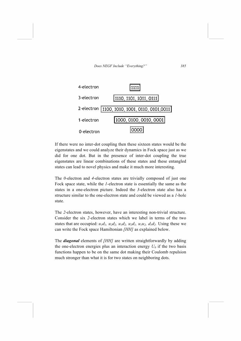
Does NEGF Include “Everything?”
385
If there were no inter-dot coupling then these sixteen states would be the eigenstates and we could analyze their dynamics in Fock space just as we did for one dot. But in the presence of inter-dot coupling the true eigenstates are linear combinations of these states and these entangled states can lead to novel physics and make it much more interesting. The 0-electron and 4-electron states are trivially composed of just one Fock space state, while the 1-electron state is essentially the same as the states in a one-electron picture. Indeed the 3-electron state also has a structure similar to the one-electron state and could be viewed as a 1-hole state. The 2-electron states, however, have an interesting non-trivial structure. Consider the six 2-electron states which we label in terms of the two states that are occupied: u1d1, u2d2, u1d2, u2d1, u1u2, d1d2. Using these we can write the Fock space Hamiltonian [HH] as explained below. The diagonal elements of [HH] are written straightforwardly by adding the one-electron energies plus an interaction energy U0 if the two basis functions happen to be on the same dot making their Coulomb repulsion much stronger than what it is for two states on neighboring dots.
Lessons from Nanoelectronics
386
[HH] =
(23.4)
The off-diagonal entries t are obtained by noting that this quantity couples the one electron states u1 to u2 and d1 to d2. With two electron states we have inserted t for non-diagonal elements that couples those states for which one state remains unchanged while the other changes from u1 to u2 or from d1 to d2. The lowest eigenstate obtained from the two-electron Hamiltonian in Eq.(23.4) is with a wavefunction of the form (s1 , s2 < 1)
(23.5)
is called the singlet state. Next comes a set of three states (called the triplets) that are higher in energy. These have the form
(23.6)
u1d1
u2d2
u1d2
u2d1
u1u2
d1d2
u1d1
u2d2
u1d2
u2d1
u1u2
d1d2
2ε1+U
00 t t 0 0
0 2ε2+U
0t t 0 0
t t ε1+ ε
20 0 0
t t 0 ε1+ ε
20 0
0 0 0 0 ε1+ ε
20
0 0 0 0 0 ε1+ ε
2
⎡
⎣
⎢⎢⎢⎢⎢⎢⎢⎢
⎤
⎦
⎥⎥⎥⎥⎥⎥⎥⎥
S : S u1d2{ }+ u
2d1{ }( )+ s1 u1d1{ }+ s2 u
2d2{ }
T1:1
2u1d2{ }− u
2d1{ }( )
T2 : u1u2{ }
T3 : d1d2{ }
Does NEGF Include “Everything?”
387
A system with two electrons is normally viewed as occupying two one-electron states. The states T2, T3 permit such a simple visualization. But the states S and T1 do not.
For example, each term in the state
permits a simple visualization: {u1d2} stands for an upspin electron in 1 and a downspin electron in 2 while {u2d1} represents an upspin in 2 and a downspin in 1. But the real state is a superposition of these two “simple” or unentangled states and there is no way to define two one-electron states a and b such that the two-electron state could be viewed as {ab}. Such states are called entangled states which comprise the key entity in the emerging new field of quantum information and computing.
How would we compute the properties of such systems? The equilibrium properties are still described by the general law of equilibrium stated earlier
pi =
1
Ze−(E
i−µN
i)/kT
(Same as Eq.(16.14))
and using the equilibrium properties to evaluate the average number of electrons.
n = Nii
∑ pi
The energies Ei are obtained by diagonalizing the Fock space Hamiltonian [HH] that we just discussed. Fig.22. Fig.23.9 shows the plot of n versus µ which looks like Fig.23.7, but the middle plateau now involves the entangled singlet state just discussed. There is also some additional structure that we will not get into. The main point we wanted to make is that the law of equilibrium statistical mechanics is quite general and can be used in this case.
T1:1
2u1d2{ }− u
2d1{ }( )
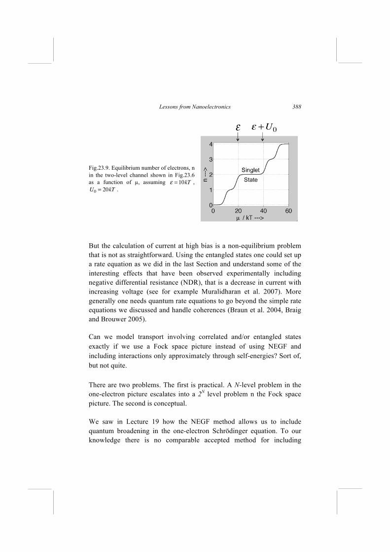
Lessons from Nanoelectronics
388
Fig.23.9. Equilibrium number of electrons, n in the two-level channel shown in Fig.23.6 as a function of µ, assuming ε = 10kT , U0 = 20kT .
But the calculation of current at high bias is a non-equilibrium problem that is not as straightforward. Using the entangled states one could set up a rate equation as we did in the last Section and understand some of the interesting effects that have been observed experimentally including negative differential resistance (NDR), that is a decrease in current with increasing voltage (see for example Muralidharan et al. 2007). More generally one needs quantum rate equations to go beyond the simple rate equations we discussed and handle coherences (Braun et al. 2004, Braig and Brouwer 2005). Can we model transport involving correlated and/or entangled states exactly if we use a Fock space picture instead of using NEGF and including interactions only approximately through self-energies? Sort of, but not quite. There are two problems. The first is practical. A N-level problem in the one-electron picture escalates into a 2N level problem n the Fock space picture. The second is conceptual. We saw in Lecture 19 how the NEGF method allows us to include quantum broadening in the one-electron Schrödinger equation. To our knowledge there is no comparable accepted method for including
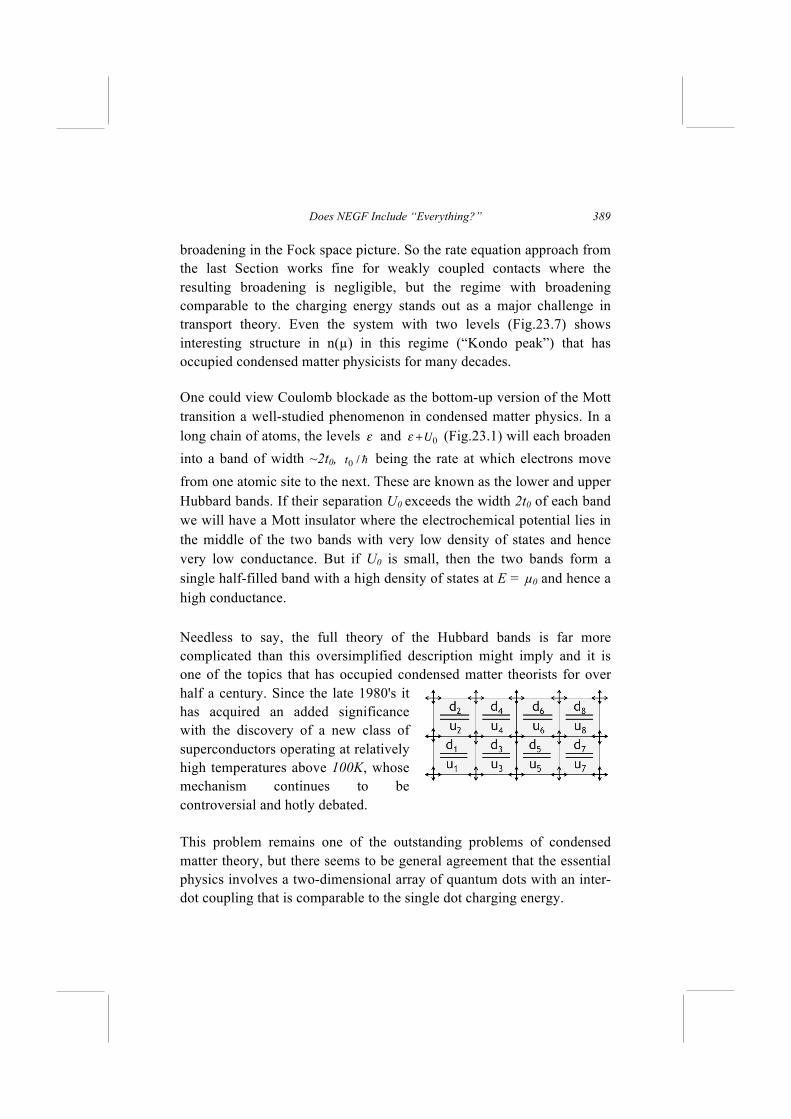
Does NEGF Include “Everything?”
389
broadening in the Fock space picture. So the rate equation approach from the last Section works fine for weakly coupled contacts where the resulting broadening is negligible, but the regime with broadening comparable to the charging energy stands out as a major challenge in transport theory. Even the system with two levels (Fig.23.7) shows interesting structure in n(µ) in this regime (“Kondo peak”) that has occupied condensed matter physicists for many decades. One could view Coulomb blockade as the bottom-up version of the Mott transition a well-studied phenomenon in condensed matter physics. In a long chain of atoms, the levels ε and ε +U0 (Fig.23.1) will each broaden into a band of width ~2t0,
t0 / being the rate at which electrons move
from one atomic site to the next. These are known as the lower and upper Hubbard bands. If their separation U0 exceeds the width 2t0 of each band we will have a Mott insulator where the electrochemical potential lies in the middle of the two bands with very low density of states and hence very low conductance. But if U0 is small, then the two bands form a single half-filled band with a high density of states at E = µ0 and hence a high conductance. Needless to say, the full theory of the Hubbard bands is far more complicated than this oversimplified description might imply and it is one of the topics that has occupied condensed matter theorists for over half a century. Since the late 1980's it has acquired an added significance with the discovery of a new class of superconductors operating at relatively high temperatures above 100K, whose mechanism continues to be controversial and hotly debated. This problem remains one of the outstanding problems of condensed matter theory, but there seems to be general agreement that the essential physics involves a two-dimensional array of quantum dots with an inter-dot coupling that is comparable to the single dot charging energy.
Lessons from Nanoelectronics
390
Lecture 24
The Quantum and the Classical
24.1. Spin coherence 24.2. Pseudo-spins 24.3. Quantum Entropy 24.4. Does Interaction Increase the Entropy? 24.5. Spins and magnets Intel has a presentation, From Sand to Circuits, on their website
http://www.intel.com/about/companyinfo/museum/exhibits/sandtocircuits/index.htm describing the amazing process that turns grains of sand into the chips that have enabled the modern information age. As I explained at the outset, these Lectures were about the physics that these “grains of sand” and the associated technology have helped illuminate in the last 25 years, the physics that helps validate the concept of an elastic resistor with a clean separation of entropy-driven processes from the force-driven ones. Interestingly much of this physics does not involve the quantum aspects and can be understood within a semiclassical picture. Nearly all of what we discussed in Parts 1 and 2 of these lectures follow from the Boltzmann equation. Even though the modern nanotransistor that powers today’s laptops is only a few hundred atoms long, it remains in essence a classical device controlled more by electrostatics than by quantum subtleties. Indeed a recent paper reports classical behavior down to atomic scale conductors (Weber et al. 2012). Is this inevitable? Or could we harness our impressive progress in nanofabrication and understanding to create a fundamentally different class of quantum devices that will take us beyond today’s charge-based information processing paradigms. Let me end these lectures with a few rambling thoughts (not answers!) on these lines.
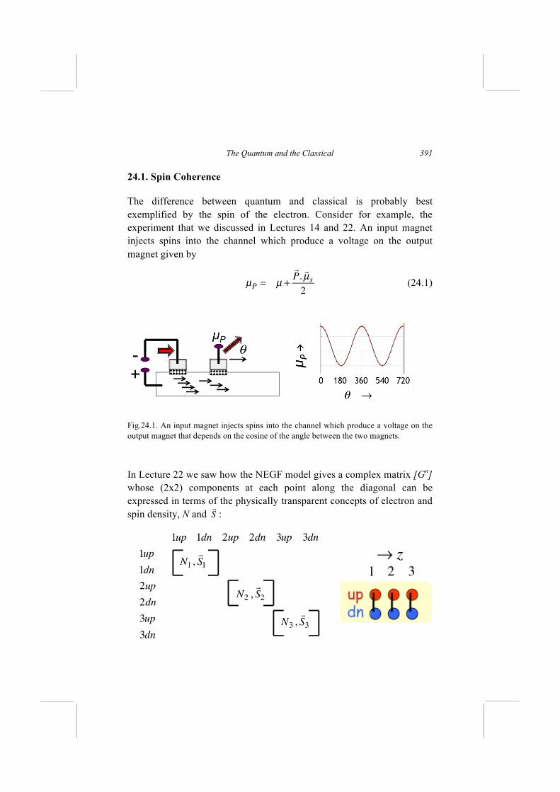
The Quantum and the Classical
391
24.1. Spin Coherence
The difference between quantum and classical is probably best exemplified by the spin of the electron. Consider for example, the experiment that we discussed in Lectures 14 and 22. An input magnet injects spins into the channel which produce a voltage on the output magnet given by
µP = µ +
P.µs
2 (24.1)
Fig.24.1. An input magnet injects spins into the channel which produce a voltage on the output magnet that depends on the cosine of the angle between the two magnets. In Lecture 22 we saw how the NEGF model gives a complex matrix [Gn] whose (2x2) components at each point along the diagonal can be expressed in terms of the physically transparent concepts of electron and spin density, N and
S :
Lessons from Nanoelectronics
392
[Gn]
2π=
N + Sz Sx − iSy
Sx + iSy N − Sz
⎡
⎣⎢⎢
⎤
⎦⎥⎥
(Same as Eq.(22.30))
The NEGF equation for current then predicts the result in Eq.(24.1), with µ and
µs related to N and
S respectively.
This simple example illustrates the relation between quantum and classical descriptions. If the transverse components of spin are negligible then we can describe the physics in terms of N and Sz only. We could interpret the non-zero components on the diagonal
(N + Sz ) as number of up electrons
(N − Sz ) as number of down electrons
(per unit energy) and then write semiclassical equations for the two types of electrons. That is essentially what we did in Lecture 14. When does this work? One possibility is that the magnets are all collinear and there is no spin-orbit coupling so that we are restricted to angles θ that are multiples of 180 degrees (Fig.24.1). Another possibility is that various spin dephasing processes are strong enough to reduce transverse components of spin to negligible proportions. And if the z-components are reduced too, then we would not have to worry about spin at all. What if we had collinear magnets but they point not along z, but along x? Now the [Gn] matrix is not diagonal
[G
n]
2π→
N Sx
Sx N
⎡
⎣⎢
⎤
⎦⎥
and it might appear that a semiclassical description is not possible. The trick is to choose the coordinates or more generally the “basis” correctly. What we should do is to select a basis in which up and down point along +x and –x respectively so that in this basis [Gn] is diagonal
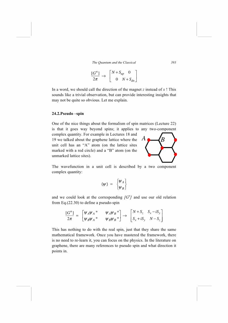
The Quantum and the Classical
393
[Gn]
2π→
N + Sup 0
0 N + Sdn
⎡
⎣⎢
⎤
⎦⎥
In a word, we should call the direction of the magnet z instead of x ! This sounds like a trivial observation, but can provide interesting insights that may not be quite so obvious. Let me explain.
24.2.Pseudo –spin
One of the nice things about the formalism of spin matrices (Lecture 22) is that it goes way beyond spins; it applies to any two-component complex quantity. For example in Lectures 18 and 19 we talked about the graphene lattice where the unit cell has an “A” atom (on the lattice sites marked with a red circle) and a “B” atom (on the unmarked lattice sites). The wavefunction in a unit cell is described by a two component complex quantity:
{ψ } =ψ A
ψ B
⎧⎨⎩
⎫⎬⎭
and we could look at the corresponding [Gn] and use our old relation from Eq.(22.30) to define a pseudo-spin
[Gn]
2π=
ψ Aψ A * ψ Aψ B *
ψ Bψ A * ψ Bψ B *
⎡
⎣⎢
⎤
⎦⎥ →
N + Sz Sx − iSySx + iSy N − Sz
⎡
⎣⎢⎢
⎤
⎦⎥⎥
This has nothing to do with the real spin, just that they share the same mathematical framework. Once you have mastered the framework, there is no need to re-learn it, you can focus on the physics. In the literature on graphene, there are many references to pseudo spin and what direction it points in.
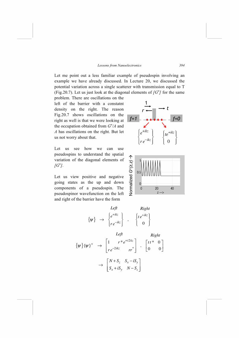
Lessons from Nanoelectronics
394
Let me point out a less familiar example of pseudospin involving an example we have already discussed. In Lecture 20, we discussed the potential variation across a single scatterer with transmission equal to T (Fig.20.7). Let us just look at the diagonal elements of [Gn] for the same problem. There are oscillations on the left of the barrier with a constatnt density on the right. The reason Fig.20.7 shows oscillations on the right as well is that we were looking at the occupation obtained from Gn/A and A has oscillations on the right. But let us not worry about that. Let us see how we can use pseudospins to understand the spatial variation of the diagonal elements of [Gn]. Let us view positive and negative going states as the up and down components of a pseudospin. The pseudospinor wavefunction on the left and right of the barrier have the form
Left
ψ{ } →e+ikz
r e−ikz
⎧⎨⎪
⎩⎪
⎫⎬⎪
⎭⎪,
Right
t e+ikz
0
⎧⎨⎪
⎩⎪
⎫⎬⎪
⎭⎪
Left
ψ{ }{ψ }+ →1 r *e
+i2kz
r e−2ikz
rr*
⎡
⎣⎢⎢
⎤
⎦⎥⎥,
Right
t t * 0
0 0
⎡
⎣⎢
⎤
⎦⎥
→N + Sz Sx − iSy
Sx + iSy N − Sz
⎡
⎣⎢⎢
⎤
⎦⎥⎥
The Quantum and the Classical
395
This suggests that the pseudospins to the left of the barrier are described by (assuming r, t are real)
Left
N = (1+ r2) / 2
Sz = (1− r2) / 2
Sx = r cos2kz
Sy = −r sin2kz
Right
N = t2/ 2
Sz = t2/ 2
Sx = 0
Sy = 0
In other words, on the left of the barrier, the pseudospin is rotating round and round in the x-y plane. When we plot Gn(z,z), we are looking at the sum of the two pseudospin components and squaring the sum, which amounts to
Trace 1 1{ } ψ{ } ψ{ }+ 1
1
⎧⎨⎩
⎫⎬⎭
= Trace1 1
1 1
⎛⎝⎜
⎞⎠⎟
ψ{ } ψ{ }+
In effect we are using a pseudomagnet with Γ =1 1
1 1
⎡
⎣⎢
⎤
⎦⎥
which corresponds to one polarized 100% along x. So from Eq.(24.1), the measured potential should be proportional to
Left Right
N + x.S →
1+ r2
2+ r cos2kz
t2
2
which describes the numerical results quite well. This is a relatively familiar problem where the concept of pseudospin probably does not add much to our undergraduate understanding of one-dimensional standing waves. The purpose was really to add our understanding of pseudospins!
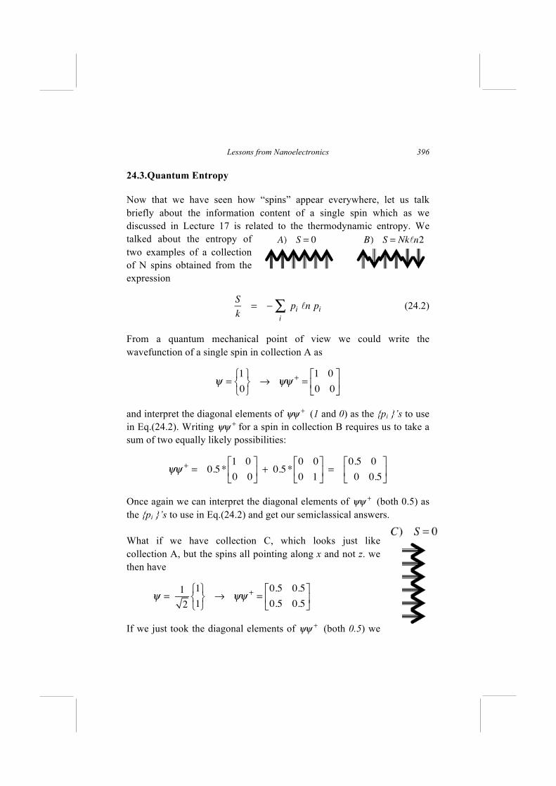
Lessons from Nanoelectronics
396
24.3.Quantum Entropy
Now that we have seen how “spins” appear everywhere, let us talk briefly about the information content of a single spin which as we discussed in Lecture 17 is related to the thermodynamic entropy. We talked about the entropy of two examples of a collection of N spins obtained from the expression
S
k= − pi
i
∑ n pi (24.2)
From a quantum mechanical point of view we could write the wavefunction of a single spin in collection A as
ψ =1
0
⎧⎨⎩
⎫⎬⎭
→ ψψ +=1 0
0 0
⎡
⎣⎢
⎤
⎦⎥
and interpret the diagonal elements of ψψ + (1 and 0) as the {pi }’s to use in Eq.(24.2). Writing ψψ + for a spin in collection B requires us to take a sum of two equally likely possibilities:
ψψ += 0.5*
1 0
0 0
⎡
⎣⎢
⎤
⎦⎥ + 0.5*
0 0
0 1
⎡
⎣⎢
⎤
⎦⎥ =
0.5 0
0 0.5
⎡
⎣⎢
⎤
⎦⎥
Once again we can interpret the diagonal elements of ψψ + (both 0.5) as the {pi }’s to use in Eq.(24.2) and get our semiclassical answers. What if we have collection C, which looks just like collection A, but the spins all pointing along x and not z. we then have
ψ =1
2
1
1
⎧⎨⎩
⎫⎬⎭
→ ψψ +=0.5 0.5
0.5 0.5
⎡
⎣⎢
⎤
⎦⎥
If we just took the diagonal elements of ψψ + (both 0.5) we
The Quantum and the Classical
397
obtain the same answer as we got for collection B which is obviously wrong. A collection with all spins pointing along x (C) should have the same entropy as a collection pointing along z (A) rather than a random collection (B). The correct answer is obtained if we first diagonalize ψψ + and then use its diagonal elements (which are the eigenvalues) as the {pi }’s in Eq.(24.2) . This is accomplished if we generalize Eq.(24.2) to write
S
k= − Trace[ρ n ρ] (24.3)
where ρ =ψψ + is a 2x2 matrix (called the density matrix).
24.3.1. How much information can one spin carry?
Suppose we decide to use the spin of the electron, that is the direction of the input magnet in Fig.24.1 to convey information. It would seem that we could send large amounts of information, since there are now many possibilities. For example, suppose we choose a set of say 64 directions of the magnetization to convey information, it would seem that the entropy would be
S / k = n64
Note that we are using 64 figuratively to represent the number of magnetization directions we use, which could just as well be 10 or 100. We have seen in Lectures 14, 22 that a magnetic voltage probe making an angle θ with the injected spins measures a voltage proportional that depends on θ (Fig.24.1) and it would seem that we could measure the direction of spin simply by measuring the voltage. This would allow us to encode 64 possible values of θ thereby transmitting
n64 rather than
n2 . But how can this be correct? Didn’t we argue earlier that for one spin
S / k = n2 rather than
n64 ? These two arguments can be reconciled
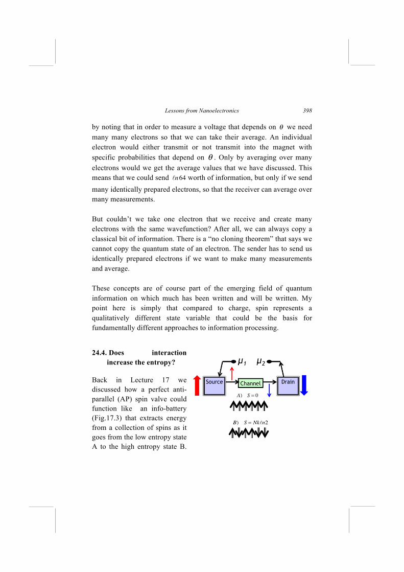
Lessons from Nanoelectronics
398
by noting that in order to measure a voltage that depends on θ we need many many electrons so that we can take their average. An individual electron would either transmit or not transmit into the magnet with specific probabilities that depend on θ . Only by averaging over many electrons would we get the average values that we have discussed. This means that we could send
n64 worth of information, but only if we send
many identically prepared electrons, so that the receiver can average over many measurements. But couldn’t we take one electron that we receive and create many electrons with the same wavefunction? After all, we can always copy a classical bit of information. There is a “no cloning theorem” that says we cannot copy the quantum state of an electron. The sender has to send us identically prepared electrons if we want to make many measurements and average. These concepts are of course part of the emerging field of quantum information on which much has been written and will be written. My point here is simply that compared to charge, spin represents a qualitatively different state variable that could be the basis for fundamentally different approaches to information processing.
24.4. Does interaction increase the entropy?
Back in Lecture 17 we discussed how a perfect anti-parallel (AP) spin valve could function like an info-battery (Fig.17.3) that extracts energy from a collection of spins as it goes from the low entropy state A to the high entropy state B.
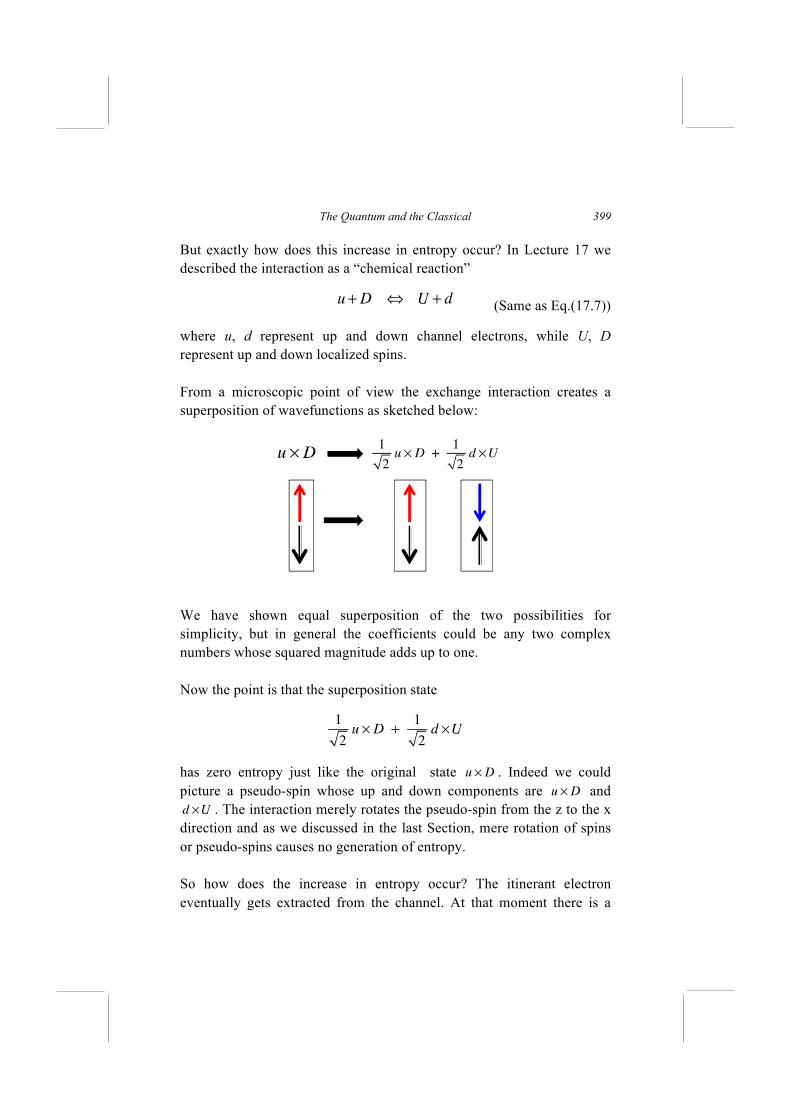
The Quantum and the Classical
399
But exactly how does this increase in entropy occur? In Lecture 17 we described the interaction as a “chemical reaction”
(Same as Eq.(17.7))
where u, d represent up and down channel electrons, while U, D represent up and down localized spins. From a microscopic point of view the exchange interaction creates a superposition of wavefunctions as sketched below: We have shown equal superposition of the two possibilities for simplicity, but in general the coefficients could be any two complex numbers whose squared magnitude adds up to one. Now the point is that the superposition state
1
2u × D +
1
2d ×U
has zero entropy just like the original state u × D . Indeed we could picture a pseudo-spin whose up and down components are u × D and d ×U . The interaction merely rotates the pseudo-spin from the z to the x direction and as we discussed in the last Section, mere rotation of spins or pseudo-spins causes no generation of entropy. So how does the increase in entropy occur? The itinerant electron eventually gets extracted from the channel. At that moment there is a
u + D ⇔ U + d
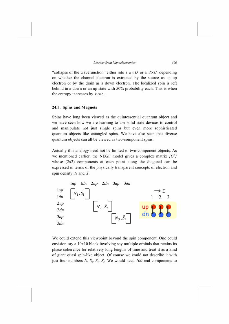
Lessons from Nanoelectronics
400
“collapse of the wavefunction” either into a u × D or a d ×U depending on whether the channel electron is extracted by the source as an up electron or by the drain as a down electron. The localized spin is left behind in a down or an up state with 50% probability each. This is when the entropy increases by
k n2 .
24.5. Spins and Magnets
Spins have long been viewed as the quintessential quantum object and we have seen how we are learning to use solid state devices to control and manipulate not just single spins but even more sophisticated quantum objects like entangled spins. We have also seen that diverse quantum objects can all be viewed as two-component spins. Actually this analogy need not be limited to two-component objects. As we mentioned earlier, the NEGF model gives a complex matrix [Gn] whose (2x2) components at each point along the diagonal can be expressed in terms of the physically transparent concepts of electron and spin density, N and
S :
We could extend this viewpoint beyond the spin component. One could envision say a 10x10 block involving say multiple orbitals that retains its phase coherence for relatively long lengths of time and treat it as a kind of giant quasi spin-like object. Of course we could not describe it with just four numbers N, Sx, Sy, Sz. We would need 100 real components to
The Quantum and the Classical
401
represent all the information contained in a 10x10 Hermitian matrix and could use the NEGF equations to come up with a diffusion equation for this 100-component object just as we discussed earlier for spin diffusion (Eq.(22.37)). Could we use these giant quasi spins to encode and transmit information? Perhaps, but there is an important lesson the last twenty years have taught us. I am talking about the integration of what used to be two distinct fields, namely spintronics and magnetics. Even ten years ago there was little overlap between these two fields. Spintronics was about the manipulation of individual spins motivated largely by basic low temperature physics, while magnetics was motivated largely by practical room temperature applications involving the manipulation of classical magnets whose magnetism is a result of enormous internal interactions that make all the elementary magnets (or spins) line up. The first step in the integration of these two fields was the use of magnetic contacts to inject spins leading to the spin valve and eventually the magnetic tunnel junctions (MTJ’s) whose change in resistance (RP to RAP, See Fig.14.1) is now routinely used to read information stored in magnets. The second step was the demonstration of spin-torque which allows injected spins to turn magnets provided they are not more than a few atomic layers in thickness. This effect could be used to write information into nanomagnets. Memory devices utilizing spin for both reading and writing are now being actively developed. The point I want to make is that for information processing it is not enough to have a spin, we also need a magnet. In standard charge-based architectures information is stored in capacitors and transmitted from capacitor to capacitor. Similarly we need a magnet to implement a spin capacitor and devices to transmit the information from magnet to
Lessons from Nanoelectronics
402
magnet. Developments in the last decade have given us the basic ingredients. Whether we can build a information processing technology around it, remains to be seen. It is tempting to go beyond simple spins and look at all kinds of exotic two-component pseudo-spins or multi-component quasi-spins that maintain phase coherence over useful lengths of time. But it seems to me that a key question one should ask is, “do we have a quasi-magnet to generate and detect the quasi-spin?” These are the kinds of questions that will probably be explored and answered in the coming years. The purpose of these notes was to try to convey the insights from the last thirty years drawn from the remarkable experiments made possible by the advances in nanoelectronics. These experiments have helped establish the elastic resistor as a useful approximation to short conductors, and we have tried to show that it can also be used to understand long conductors by viewing them approximately as combinations of elastic resistors. As I stated in the introductory lecture, I believe that the results we have discussed all follow directly from the formal theories of semiclassical or quantum transport. The real value of the bottom-up approach based on elastic resistors is in improving our physical understanding, and this will hopefully facilitate the insights needed to take us to the next level of understanding, discovery and innovation. The last thirty years have taught us the significance of contacts, even the most mundane ones. We have also seen some of the interesting things that can be achieved with “smarter” contacts like the magnetic ones. Perhaps in the coming years we will learn to manipulate and control them creatively so that they become an active part of information processors.


