Embed Size (px)
Citation preview
!"#$" %&'()*#$ +# !$$ "
! " #$ # % &'( ) $ # "*%) )# !+" # # !)"*%)## ,"-."!/01+234# !"
Ω
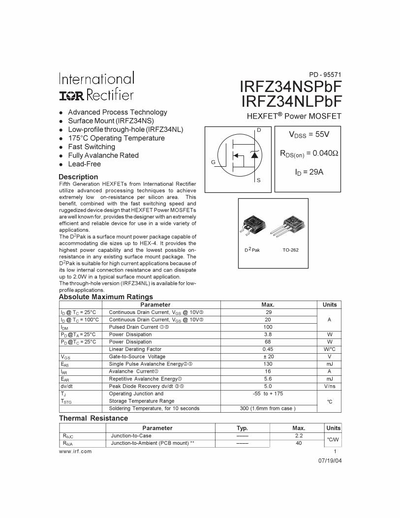
2 D Pak TO-262
S
D
G
θ θ
!"# $%%% &' (' ) !"( $%%% &' (' * +$%%% ( !"# , % $- ./ !"# , % $- 0/
1 %$ %23% # ' 4 5% '*2 6 '7 52* * 8*9 7 %2: (. 8*9 %% (0
7 - 8 8*9 7 %2: #0 +8+ ;$+ 8 %:+8+ # '! <- %2+ ##=(>#! 5%2 ! - %% 2
5*+ %2! - %% & ?%( + .(0?%
,,,%? (
,,,%?
9 +(@A% 3%4(B %*3%% + +?-%+*+ %2 9A % ? %--* CD))
! "#
' $%5% % ;+, '*2 ## ' '"'&"#E
∆∆ % ;+,'*2 ! - ?? # ' ? % #&"( 5 $%5% < Ω '"('&"(0
' 4 !9% 9*+'*2 ' '"'&"#E2 3%,%+ !%+ 0# 5 '"#'&"(0
# '"##'&'"' # '"'&'"'&!"(#
4 5% 3%,%+ 1 ;2 ( '"'4 5% 8 % 1 ;2 ( '"'
F !*4 9%2 . "(0F 4 5% 9%2 0/ '"'
F 4 $%@B** %@9%2 ( '"('&5 320+(.
!%<$ *:! > '"/'
! ) "(0 !%<??$ *:! .( "(/Ω 3**! "(/Ω, 5 32(
, * +&
+ %?+ -- > '"' <-- -3 '"#'
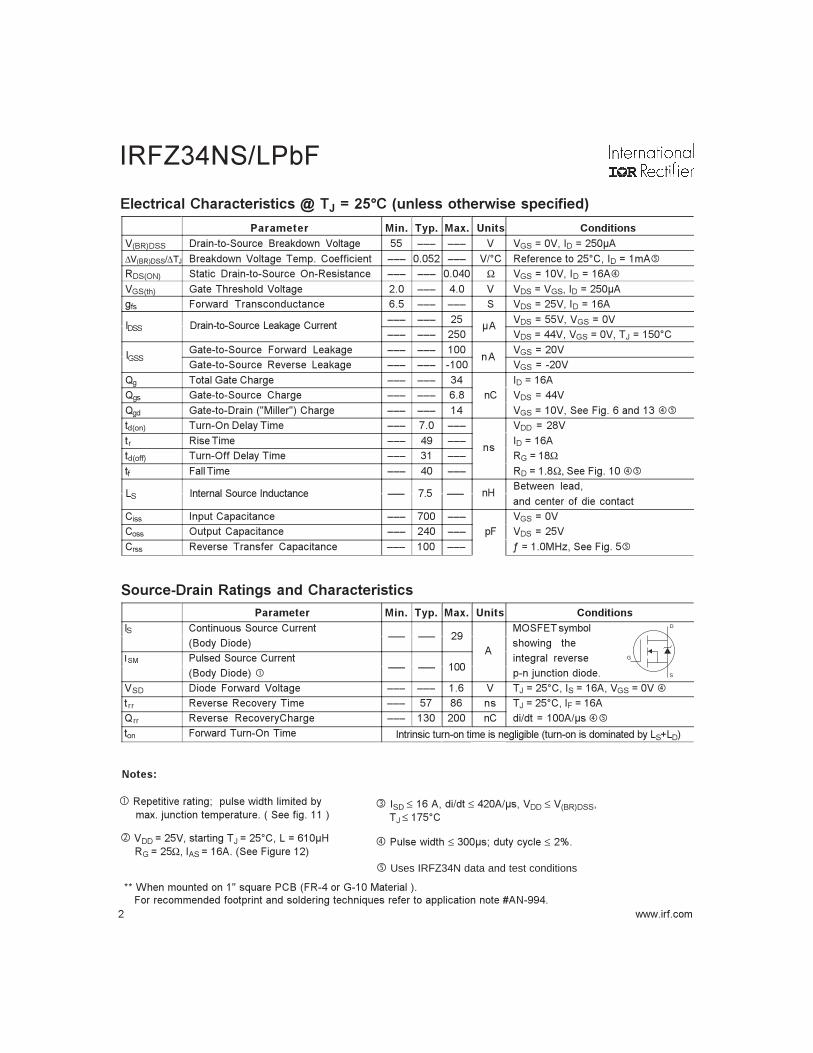
8 % !%? % - ( G"(BHI&5 32#
$%5% 1 ;2 %%
E
H1 %*5% + >#
- 8 %2J-* ,+9* +:KL - %% 5 ?2((
ISD ≤(0&++≤E&'≤' &!≤(>#
5% %% B<537!:*+:$+ 9,2 9
* +5% %% 2%* % 8 % +:$+ -L++
' $+ 3%,%+ '*2 (0 ' !"#&"(0&'"' 8 % 8 %:! #> /0 !"#&"(0F 8 % 8 %:9%2 (. ++"(E
3%,%+!%<!
$% "
%% 2*2* %+ +:1=1
(
)
S
D
G
'"#'&%2!"#&1"0(EH"#Ω&"(05 32% (
* ,+9≤ .EJ+::* ≤M
Uses IRFZ34N data and test conditions
,,,%? .
1
10
100
1000
0.1 1 10 100
I ,
Dra
in-t
o-S
ourc
e C
urre
nt (
A)
D
V , Drain-to-Source Voltage (V)DS
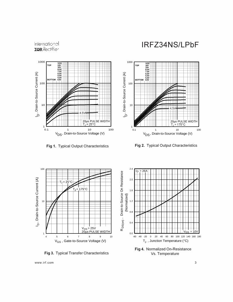
VGS TOP 15V 10V 8.0V 7.0V 6.0V 5.5V 5.0V BOTTOM 4.5V
20µs PULSE WIDTH T = 25°CC A
4.5V
1
10
100
1000
0.1 1 10 100
I ,
Dra
in-t
o-S
ourc
e C
urre
nt (
A)
D
V , Drain-to-Source Voltage (V)DS
VGS TOP 15V 10V 8.0V 7.0V 6.0V 5.5V 5.0V BOTTOM 4.5V
A
4.5V
20µs PULSE WIDTH T = 175°CC
1
10
100
4 5 6 7 8 9 10
T = 25°CJ
GSV , Gate-to-Source Voltage (V)
DI ,
Dra
in-t
o-S
our
ce C
urre
nt (
A)
A
V = 25V 20µs PULSE WIDTH
T = 175°CJ
DS
0.0
0.4
0.8
1.2
1.6
2.0
2.4
-60 -40 -20 0 20 40 60 80 100 120 140 160 180
JT , Junction Temperature (°C)
R
, D
rain
-to-
Sou
rce
On
Res
ista
nce
DS
(on)
(Nor
mal
ized
)
V = 10VGSA
I = 26AD
!
!"# !"(>#
,,,%?
" #$ %
&'"%(
!" %
)% !)" %
0
200
400
600
800
1000
1200
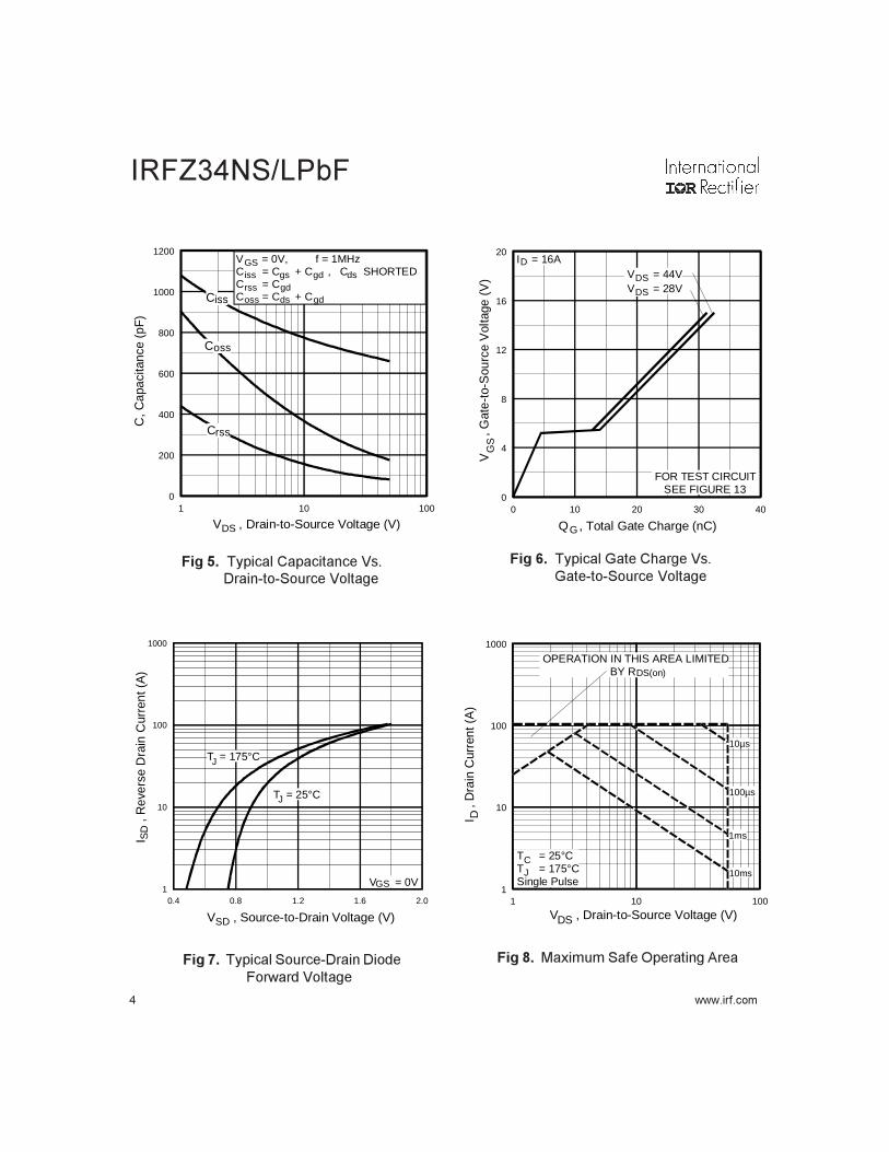
1 10 100
C, C
apac
itanc
e (p
F)
DSV , Drain-to-Source Voltage (V)
A
V = 0V, f = 1MHzC = C + C , C SHORTEDC = CC = C + C
GSiss gs gd dsrss gdoss ds gdCiss
Coss
Crss
0
4
8
12
16
20
0 10 20 30 40
Q , Total Gate Charge (nC)G
V
, G
ate-
to-S
ourc
e V
olta
ge (
V)
GS
A
FOR TEST CIRCUIT SEE FIGURE 13
V = 44VV = 28V
DS
DS
I = 16AD
1
10
100
1000
0.4 0.8 1.2 1.6 2.0
T = 25°CJ
V = 0VGS
V , Source-to-Drain Voltage (V)
I
, Rev
erse
Dra
in C
urre
nt (
A)
SD
SD
A
T = 175°CJ
1
10
100
1000
1 10 100
V , Drain-to-Source Voltage (V)DS
I ,
Dra
in C
urre
nt (
A)
OPERATION IN THIS AREA LIMITED BY R
D
DS(on)
10µs
100µs
1ms
10ms
A
T = 25°CT = 175°C Single Pulse
CJ
,,,%? #
"$ %
+-
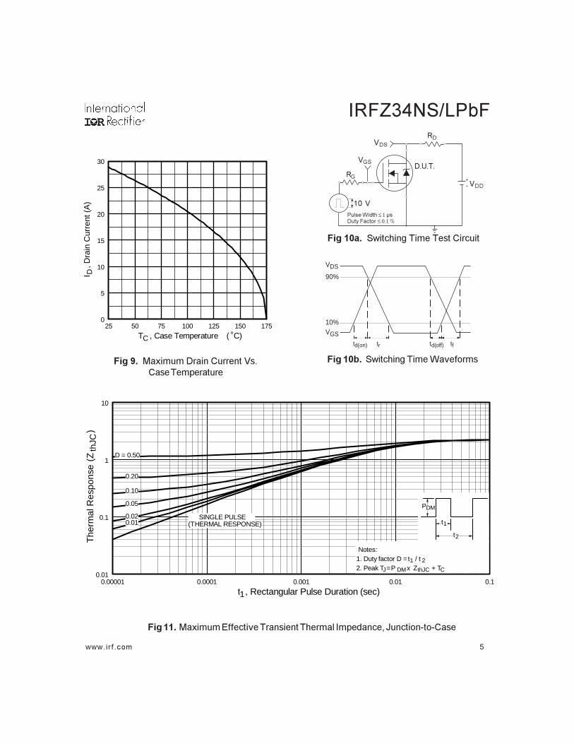
VDS
90%
10%VGS
td(on) tr td(off) tf
'
('
≤ 1 !"#≤ 0.1 %
&' !
"$ %*+
'
'
$N!
&', +- ./
25 50 75 100 125 150 1750
5
10
15
20
25
30
T , Case Temperature ( C)
I ,
Dra
in C
urre
nt (
A)
°C
D
0.01
0.1
1
10
0.00001 0.0001 0.001 0.01 0.1
Notes:1. Duty factor D =t / t2. Peak T =P x Z + T
1 2
J DM thJC C
P
t
t
DM
1
2
t , Rectangular Pulse Duration (sec)
The
rmal
Res
pons
e(Z
)
1
thJC
0.010.02
0.05
0.10
0.20
D = 0.50
SINGLE PULSE(THERMAL RESPONSE)
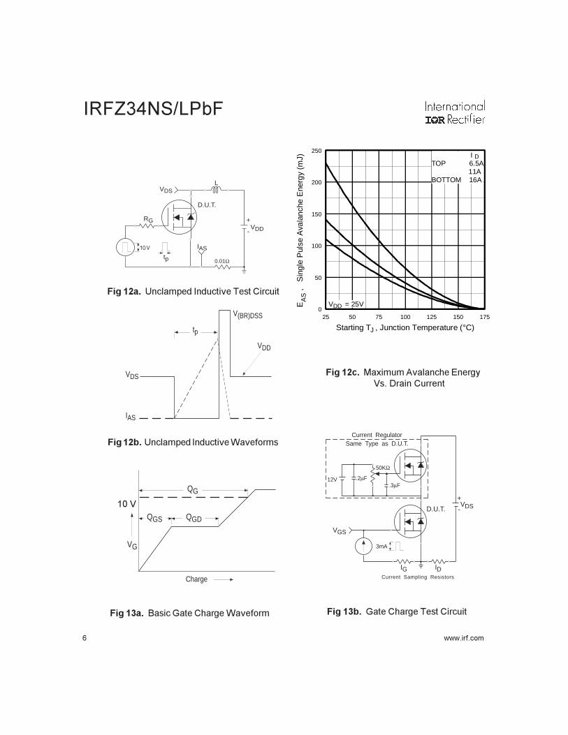
0 ,,,%?
0 - +
0 - +*+
1 )%*+
tp
VDS
IAS
VDD
V(BR)DSS
D.U.T.VDS
IDIG
3mA
VGS
.3µF
50KΩ
.2µF12V
Current RegulatorSame Type as D.U.T.
Current Sampling Resistors
+
-
QG
QGS QGD
VG
Charge
2
0
50
100
150
200
250
25 50 75 100 125 150 175
J
E
,
Sin
gle
Pul
se A
vala
nche
Ene
rgy
(mJ)
AS
A
Starting T , Junction Temperature (°C)
V = 25V
ITOP 6.5A 11ABOTTOM 16A
DD
D
VDSL
D.U.T.
VDD
IAS
tp 0.01Ω
RG +
-
$%&
)%
&'(+ ,% !
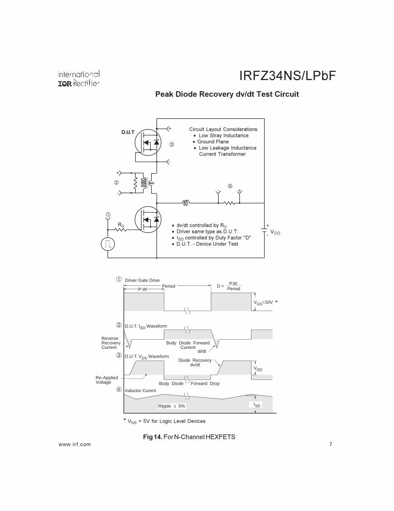
,,,%? >
P.W.Period
di/dt
Diode Recoverydv/dt
Ripple ≤ 5%
Body Diode Forward DropRe-AppliedVoltage
ReverseRecoveryCurrent
Body Diode ForwardCurrent
VGS=10V
VDD
ISD
Driver Gate Drive
D.U.T. ISD Waveform
D.U.T. VDS Waveform
Inductor Curent
D = P.W.Period
+
-
+
+
+-
-
-
#3,4#,"
5'"#'?%121 8 *$ 8
'
• +8+%** +:• $%8 % :- $N!• %** +:$:3%@$@• $N!$ 8 N+ %!
%1:+ % • 1,5%:+ • 4%+* • 1,1 ;2 + %% !%?% %
5
/ ,,,%?
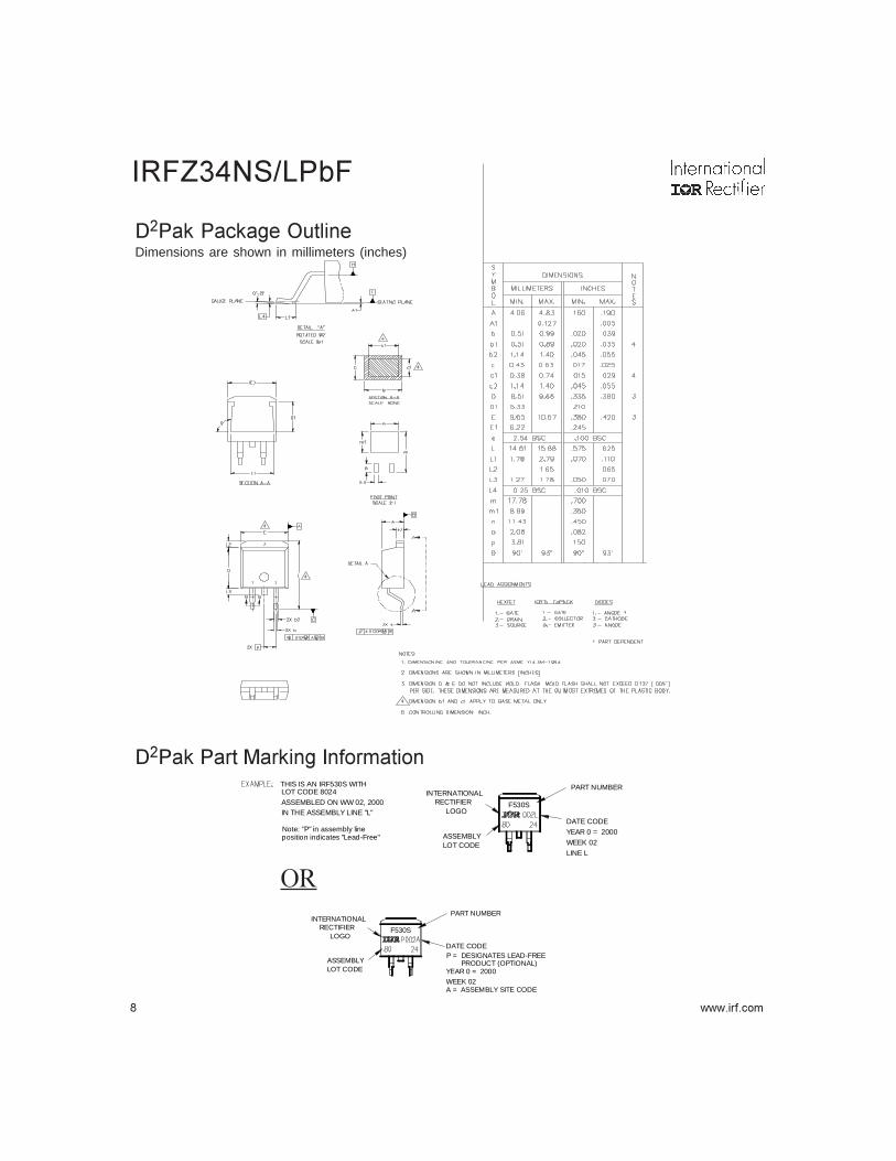
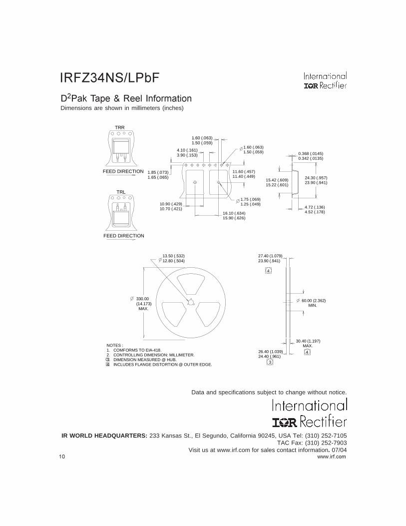
Dimensions are shown in millimeters (inches)
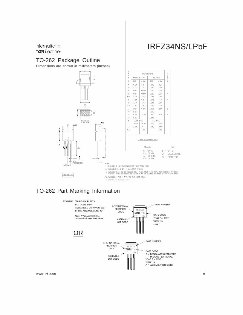
Note: "P" in as sembly linepos ition indicates "Lead-Free"
F 530S
T HIS IS AN IRF530S WITHLOT CODE 8024ASS EMBLED ON WW 02, 2000IN THE ASSE MBLY L INE "L"
ASSE MBLYLOT CODE
INTE RNATIONALRECT IFIE R
LOGO
PART NUMBER
DAT E CODEYEAR 0 = 2000WEEK 02LINE L
F530S
A = AS S EMBLY SITE CODEWEEK 02
P = DES IGNAT ES LEAD-FREEPRODUCT (OPT IONAL)
RECT IF IERINT ERNAT IONAL
LOGO
LOT CODEASS EMBLY
YEAR 0 = 2000
DATE CODE
PART NUMBER
,,,%? )
TO-262 Part Marking Information
TO-262 Package OutlineDimensions are shown in millimeters (inches)
AS SEMBLYLOT CODE
RECT IF IERINTERNATIONAL
AS SEMBLED ON WW 19, 1997
Note: "P" in assembly lineposition indicates "Lead-Free"
IN THE ASS EMBLY LINE "C" LOGO
THIS IS AN IRL3103LLOT CODE 1789
EXAMPLE:
LINE C
DATE CODE
WEEK 19YEAR 7 = 1997
PART NUMBER
PART NUMBER
LOGO
LOT CODEASS EMBLY
INTERNAT IONALRECTIFIER
PRODUCT (OPTIONAL)P = DESIGNATES LEAD-FREE
A = AS SEMBLY S ITE CODEWEEK 19YEAR 7 = 1997
DATE CODE
OR
( ,,,%?
Dimensions are shown in millimeters (inches)
3
4
4
TRR
FEED DIRECTION
1.85 (.073)1.65 (.065)
1.60 (.063)1.50 (.059)
4.10 (.161)3.90 (.153)
TRL
FEED DIRECTION
10.90 (.429)10.70 (.421)
16.10 (.634)15.90 (.626)
1.75 (.069)1.25 (.049)
11.60 (.457)11.40 (.449)
15.42 (.609)15.22 (.601)
4.72 (.136)4.52 (.178)
24.30 (.957)23.90 (.941)
0.368 (.0145)0.342 (.0135)
1.60 (.063)1.50 (.059)
13.50 (.532)12.80 (.504)
330.00(14.173) MAX.
27.40 (1.079)23.90 (.941)
60.00 (2.362) MIN.
30.40 (1.197) MAX.
26.40 (1.039)24.40 (.961)
NOTES :1. COMFORMS TO EIA-418.2. CONTROLLING DIMENSION: MILLIMETER.3. DIMENSION MEASURED @ HUB.4. INCLUDES FLANGE DISTORTION @ OUTER EDGE.
Data and specifications subject to change without notice.
IR WORLD HEADQUARTERS: 233 Kansas St., El Segundo, California 90245, USA Tel: (310) 252-7105TAC Fax: (310) 252-7903
Visit us at www.irf.com for sales contact information. 07/04

Note: For the most current drawings please refer to the IR website at: http://www.irf.com/package/

Mouser Electronics
Authorized Distributor
Click to View Pricing, Inventory, Delivery & Lifecycle Information: Infineon:
IRFZ34NSPBF IRFZ34NSTRRPBF IRFZ34NSTRLPBF


