Embed Size (px)
Citation preview

© 2021 Toshiba Electronic Devices & Storage Corporation Confidential
TC358840XBG / TC358870XBGProcess Change Notice of wafer-fab site
Jan 26, 2021
System Devices Customer Quality Group
Semiconductor Quality Div.
Digital Product Dept.
System Devices Div.
Toshiba Electronic Devices & Storage Corporation SMC-OP20B0134-SM1

2© 2021 Toshiba Electronic Devices & Storage Corporation Confidential
Summary
(1) Overview
Toshiba has outsourced wafer-fab process of the target products to Sony Semiconductor
Manufacturing Corporation (hereinafter referred to as “SCK”) in Oita Japan since 2016. However,
considering stable and long term supply, Toshiba has decided to change wafer-fab site from SCK to
Samsung Foundry (hereinafter referred to as “SF”).
(2) Changes and timing
Regarding changes and its timing, please refer following table.
(3) Target Products
TC358840XBG / TC358870XBG
ProcessChanges
Timing DetailFrom To Category
40nmSCK Japan(Sony Semiconductor
Manufacturing Corporation)
SF Korea
(Samsung Foundry)Wafer-fab site change Mar. 2022
This change will involve change
in 5M1E.
Wafer-fab process technology
and design will be unchanged.

3© 2021 Toshiba Electronic Devices & Storage Corporation Confidential
Contents
Overview
Changes and evaluation plan
01
02

4© 2021 Toshiba Electronic Devices & Storage Corporation Confidential
01Overview
Outsourcing, Switching plan

5© 2021 Toshiba Electronic Devices & Storage Corporation Confidential
Wafer-fab site
Wafer-fab site will be changed from SCK(Japan) to SF(Korea) from Apr. 2022
Samsung Foundry
SF : Samsung Foundry
Sony Semiconductor Manufacturing Corporation
After
Apr. 2022
Incheon
Seoul
Giheung
SamsungFoundry
Wafer-fab Wafer test Assembly Final test
Change target No change No change No change

6© 2021 Toshiba Electronic Devices & Storage Corporation Confidential
Overview of Samsung Foundry(=SF)
Location Giheung, Korea
Establishment April. 2004
Site area 50,710m2
Employees 2,578
MP start
(40nm process)July, 2009
Capacity
(40nm process)
Over 30k wafer
per month
General information
S1 Fab
2009 2010 2011 2012 ・・・ 2019 2020 2021
Process setup
(consumer)
Process setup
Proto/EV Production
Complete
History & Setup status for automotive products
Process porting was started from 2009, as a backup manufacturing
line for Toshiba standard 40nm process, and completed in 2011.
Production has been continued as of today for consumer products.
(Total production quantity is over 85k wafers as of January 2020).
Process porting means tune-up of the manufacturing process
without any design change so that it can be the equivalent process
to the original one.
Toshiba can transfer the 40nm product without design change.

7© 2021 Toshiba Electronic Devices & Storage Corporation Confidential
What is the “Process porting” ?
Process is tuned to the original one without any change on circuit and layout.
Product design
CAD process
Mask make
Wafer make
Wafer test
Go to assembly step
Definition of process porting Tune up the manufacturing process of other site to be the same
electrical characteristics as Toshiba original manufacturing process
without any product design change.
Changes
Chip size, electrical characteristics and test pattern for outgoing test
are not changed because of no change in circuit and design. However,
5M1E will be changed because manufacturing process, material and
equipment are changed to the new wafer-fab site’s standards. Also,
photo masks will be re-made to adapt to the lithography equipment
on the process porting site.

8© 2021 Toshiba Electronic Devices & Storage Corporation Confidential
Item Before after
TSB name TC358870XBG(EL,H2) TC358870XBG(XE,H2)
Customername
Label
Product identification for TC358870XBG(EL,H2)
Product and label can be identified.There is no mixing with existing products in the same package.
HAF
HAF
(XE,H2)KOREA
Change:
9© 2021 Toshiba Electronic Devices & Storage Corporation Confidential
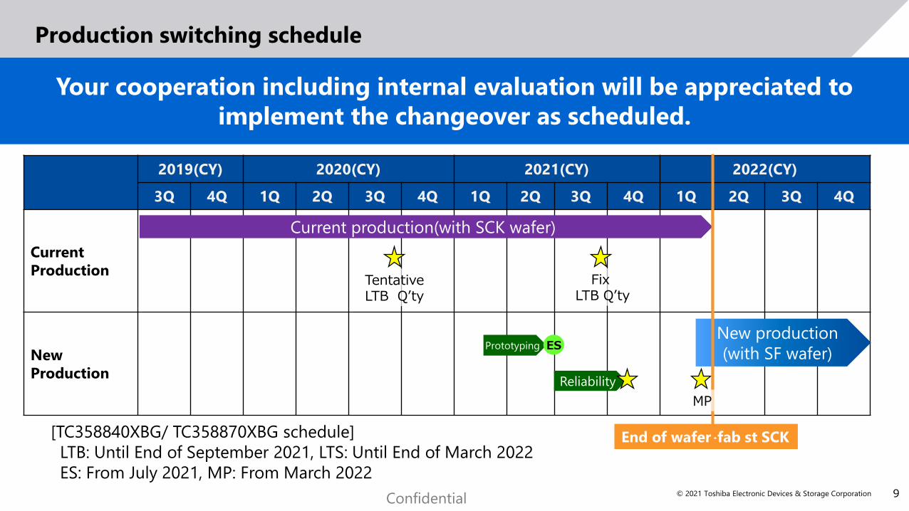
Production switching schedule
Your cooperation including internal evaluation will be appreciated to
implement the changeover as scheduled.
[TC358840XBG/ TC358870XBG schedule]
LTB: Until End of September 2021, LTS: Until End of March 2022
ES: From July 2021, MP: From March 2022
2019(CY) 2020(CY) 2021(CY) 2022(CY)
3Q 4Q 1Q 2Q 3Q 4Q 1Q 2Q 3Q 4Q 1Q 2Q 3Q 4Q
Current
Production
New
Production
Current production(with SCK wafer)
End of wafer-fab st SCK
New production
(with SF wafer)Prototyping ES
Reliability
Fix LTB Q’ty
TentativeLTB Q’ty
MP

10© 2021 Toshiba Electronic Devices & Storage Corporation Confidential
02Change Point and evaluation items involved in This Site Change

11© 2021 Toshiba Electronic Devices & Storage Corporation Confidential
Change Point Involved in This Change
We will proceed with evaluation focusing on the change point involved in this change.
■Comparison of manufacturing site (Change point analysis by 5M1E)
5M1E Change point between SCK and SF Evaluation items
Man Operators at SCK will be changed to the ones at SF. Operator certification
Machine Machines at SCK will be changed to the ones existing at SF. Electrical characteristic, Product reliability
Measurement Measurement tool will be changed. Electrical characteristic
MethodProcess flow will be changed.
Equivalent process performance will be secured by process porting.Electrical characteristic, Product reliability
Material Material will be changed to the one tried-and-true at SF. Electrical characteristic, Product reliability
Environment Environment will be changed to the one tried-and-true at SF. Clean room Environment
Evaluation items Change Change point between SCK and SF
Product specification(Electrical items) No No change in Product specification.
IC chip (Design rule, Circuit design, Chip size) No No change in Design rule, Circuit design, Chip size.
Quality assurance, Failure analysis organization No No change in Quality assurance, Failure analysis organization.
■Change point in product

12© 2021 Toshiba Electronic Devices & Storage Corporation Confidential
Reliability Test Plan
No Item Test Condition Sample size Criteria
1 Pre-conditioning [MRT]*1Bake(125deg.C/24h), 30deg.C/70%RH/216h,
Air/IR Reflow 260deg.C max, 4times.25pcs/3Lot 0 failure
2 Temperature cycle [TCT] *1 -55deg.C~125deg.C/700cyc 25pcs/3Lot 0 failure
3High humidity and high pressure
[UHAST] *1110deg.C/85%/264h 25pcs/3Lot 0 failure
4 High temperature storage [HTS] *1 150deg.C/1000h 25pcs/3Lot 0 failure
5High temperature and high humidity
operation [THB] *185deg.C/85%/1000h 25pcs/3Lot 0 failure
6 ESD[HBM] +/-2000V 3pcs/1Lot 0 failure
7 ESD[CDM] +/-500V 3pcs/1Lot 0 failure
8 ESD[MM] +/-200V 3pcs/1Lot 0 failure
9 Latch-Up[LU] (Current pulse) +/-50mA@RT 3pcs/1Lot 0 failure
10 Latch-Up[LU](Power supply overvoltage) Maximum rating 3pcs/1Lot 0 failure
We will proceed the following evaluation
*1: Acting for the results of representative products

13© 2021 Toshiba Electronic Devices & Storage Corporation Confidential
Conclusion
- For this site change, we will work in cooperation with our outsourcer Samsung
Foundry.
- We will determine whether or not to implement the change based on the results
of facilities setup verification and product evaluations at the new site, and then
inform you about our conclusion for the changeover.
We will focus on the facilities/product setup to ensure continuous supply of
products that you can use without any concern.
- If you have question and/or request regarding this change, you are kindly
requested to inform our sales representative in charge.
You are also requested to consider and provide with your required quantities of
the ongoing product.

14© 2021 Toshiba Electronic Devices & Storage Corporation Confidential


