Embed Size (px)
Citation preview
1
Department of Physics Nirmala College Muvattupuzha
Laboratory Manual for BSc. Physics Model 2 (Semester 2)
Applied electronics
2017-2020
Compiled and Edited
by
Dr. Aloysius Sabu N
Associate Professor of Physics

2
1. Characteristics of Junction Field Effect Transistor (JFET)
Aim: To study the Drain and Transfer Characteristics of a Junction Field Effect Transistor (JFET).
Components: JFET (BFW10), Bread board, Regulated Power supply (0 - 2 V) and (0 - 12 V), Ammeters (0
- 20 mA), Voltmeter V1 (0 - 2V), Voltmeter V2, (0 - 10V), Connecting wires (Single Strand)
Theory and Operation: 1. Drain characteristics are obtained between the drain to source voltage (VDS) and drain
current (ID) taking gate to source voltage (VGS) as the constant parameter.
2. Transfer characteristics are obtained between the gate to source voltage (VGS) and drain
current (ID) taking drain to source voltage (VDS) as the constant parameter.
FET Parameters
1. Drain Resistance (rd): It is given by the relation of small change in drain to source
voltage ( VDS) to the corresponding change in Drain Current ( ID) for a constant gate
to source voltage ( VGS), when the JFET is operating in pinch-off region.
𝑟𝑑 = ∆𝑉𝐷𝑆
∆𝐼𝐷 at a constant VGS (from drain characteristics)
2. Trans Conductance (gm): Ratio of small change in drain current ( ID) to the
corresponding change in gate to source voltage ( VGS) for a constant VDS.
𝑔𝑚 = ∆𝐼𝐷
∆𝑉𝐺𝑆 at constant VDS (from transfer characteristics).
The value of gm is expressed in mho’s ( ) or Siemens (s).
3. Amplification factor (µ): It is given by the ratio of small change in drain to source
voltage ( VDS) to the corresponding change in gate to source voltage ( VGS) for a
constant drain current (ID).
𝝁 = (∆𝑽𝑫𝑺
∆𝑰𝑫 ) × (
∆𝑰𝑫
∆𝑽𝑮𝑺) =
∆𝑽𝑫𝑺
∆𝑽𝑮𝑺
𝑖𝑒. 𝝁 = 𝒓𝒅 × 𝒈𝒎
Pin assignment of FET:
3
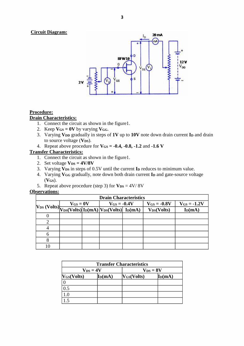
Circuit Diagram:
Procedure:
Drain Characteristics: 1. Connect the circuit as shown in the figure1.
2. Keep VGS = 0V by varying VGG.
3. Varying VDD gradually in steps of 1V up to 10V note down drain current ID and drain
to source voltage (VDS).
4. Repeat above procedure for VGS = -0.4, -0.8, -1.2 and -1.6 V
Transfer Characteristics: 1. Connect the circuit as shown in the figure1.
2. Set voltage VDS = 4V/8V
3. Varying VDS in steps of 0.5V until the current ID reduces to minimum value.
4. Varying VGG gradually, note down both drain current ID and gate-source voltage
(VGS).
5. Repeat above procedure (step 3) for VDS = 4V/ 8V
Observations:
Drain Characteristics
VDS (Volts) VGS = 0V VGS = -0.4V VGS = -0.8V VGS = -1.2V
VDS(Volts) ID(mA) VDS(Volts) ID(mA) VDS(Volts) ID(mA)
0
2
4
6
8
10
Transfer Characteristics
VDS = 4V VDS = 8V
VGS(Volts) ID(mA) VGS(Volts) ID(mA)
0
0.5
1.0
1.5

4
Graph:
1. Plot the drain characteristics by taking VDS on X-axis and ID on Y-axis at a constant
VGS.
2. Plot the transfer characteristics by taking VGS on X-axis and taking ID on Y-axis at
constant VDS.
Calculations from Graph:
1. Drain Resistance (rd):
𝑟𝑑 = ∆𝑉𝐷𝑆
∆𝐼𝐷 at a constant VGS (from drain characteristics)
2. Trans Conductance (gm):
𝑔𝑚 = ∆𝐼𝐷
∆𝑉𝐺𝑆 at constant VDS (from transfer characteristics).
The value of gm is expressed in mho’s ( ) or Siemens (s).
3. Amplification factor (µ): It is given by the ratio of small change in drain to source
voltage ( VDS) to the corresponding change in gate to source voltage ( VGS) for a
constant drain current (ID).
𝝁 = (∆𝑽𝑫𝑺
∆𝑰𝑫 ) × (
∆𝑰𝑫
∆𝑽𝑮𝑺) =
∆𝑽𝑫𝑺
∆𝑽𝑮𝑺
𝑖𝑒. 𝝁 = 𝒓𝒅 × 𝒈𝒎
Result: Drain and Transfer characteristics of a FET are studied.
Outcomes: Students are able to
1. Analyze the Drain and transfer characteristics of FET in Common Source
configuration.
2. Calculate the parameters transconductance (gm), drain resistance (rd) and
amplification factor (µ).
5
2. Characteristics of Uni-Junction Transistor (UJT)
Aim:
To study and plot the characteristics of UJT
Components: UJT 2N 2646, Resistors (1 K ohm), Bread board, Regulated Power supply (0 -
2 V) and (0 - 12 V), Ammeters (0 - 20 mA), Voltmeter (0 - 2V), Voltmeter (0 - 10V),
Connecting wires (Single Strand)
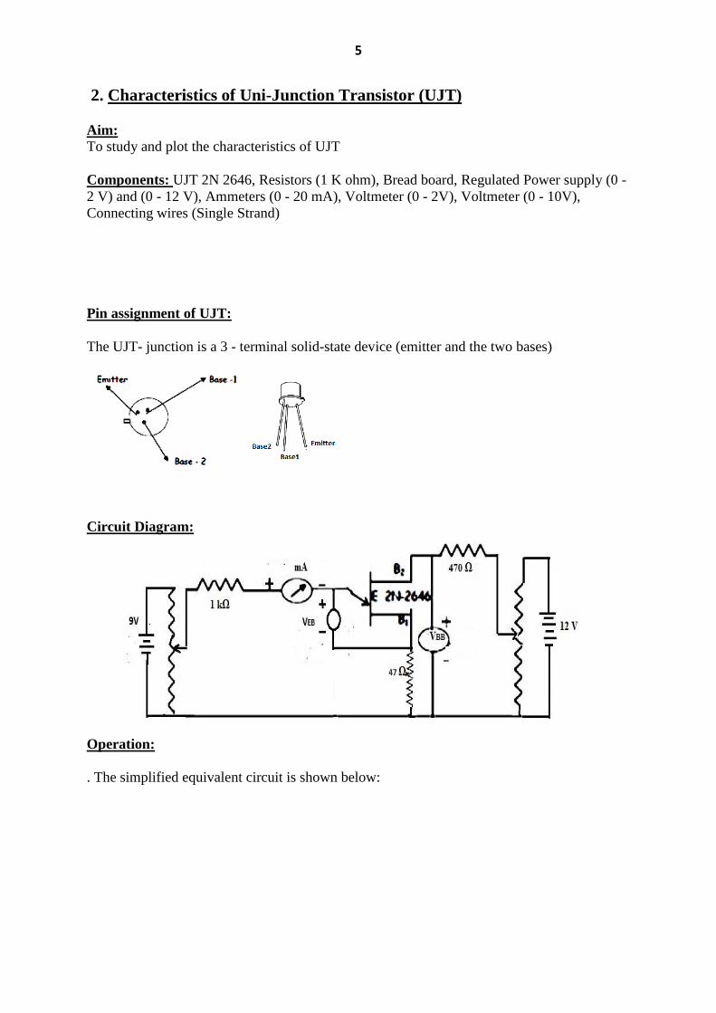
Pin assignment of UJT:
The UJT- junction is a 3 - terminal solid-state device (emitter and the two bases)
Circuit Diagram:
Operation:
. The simplified equivalent circuit is shown below:
6
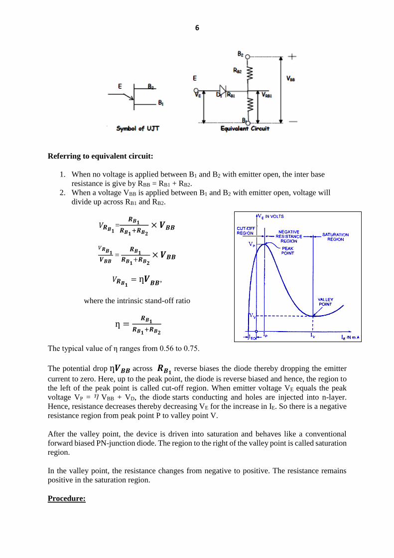
Referring to equivalent circuit:
1. When no voltage is applied between B1 and B2 with emitter open, the inter base
resistance is give by RBB = RB1 + RB2.
2. When a voltage VBB is applied between B1 and B2 with emitter open, voltage will
divide up across RB1 and RB2.
𝑉𝑹𝑩𝟏=
𝑹𝑩𝟏
𝑹𝑩𝟏+𝑹𝑩𝟐
× 𝑽𝑩𝑩
𝑉𝑹𝑩𝟏
𝑽𝑩𝑩 =
𝑹𝑩𝟏
𝑹𝑩𝟏+𝑹𝑩𝟐
× 𝑽𝑩𝑩
𝑉𝑹𝑩𝟏= ƞ𝑽𝑩𝑩,
where the intrinsic stand-off ratio
ƞ =𝑹𝑩𝟏
𝑹𝑩𝟏+𝑹𝑩𝟐
The typical value of η ranges from 0.56 to 0.75.
The potential drop ƞ𝑽𝑩𝑩 across 𝑹𝑩𝟏 reverse biases the diode thereby dropping the emitter
current to zero. Here, up to the peak point, the diode is reverse biased and hence, the region to
the left of the peak point is called cut-off region. When emitter voltage VE equals the peak
voltage VP = VBB + VD, the diode starts conducting and holes are injected into n-layer.
Hence, resistance decreases thereby decreasing VE for the increase in IE. So there is a negative
resistance region from peak point P to valley point V.
After the valley point, the device is driven into saturation and behaves like a conventional
forward biased PN-junction diode. The region to the right of the valley point is called saturation
region.
In the valley point, the resistance changes from negative to positive. The resistance remains
positive in the saturation region.
Procedure:

7
1. Connect the circuit as shown in the circuit diagram.
2. Set output voltage VBB = 8V by varying VBB.
3. Varying VEE gradually, note down both emitter current IE and emitter voltage (VE).
4. Step size is not fixed because of non linear curve. Initially Vary VEE in steps of 1V.
Current IE remains zero. As voltage is varied further, current starts increasing while
voltage VE drops. Note down the readings VE and IE.
5. Repeat above procedure (step 3) for VBB = 10V.
6. Plot the tabulated readings on a graph sheet with IE on X-axis and VE on Y-axis.
Observations:
VBB = 8V VBB = 10V
IE(mA) VE(V) IE(mA) VE(V)
Inference:
1. There is a negative resistance region from peak point to valley point.
2. Increase in VBB increases the value of peak and valley voltages.
Result:
The emitter characteristics of UJT are studied.
a. Peak Voltage, Vp ___________ Volts.
b. Valley Voltage, Vv ___________ Volts.
c. Valley Current, Iv ___________ mA.
d. Negative Resistance ___________ Ohms
e. Intrinsic stand-off ratio η -----------------
Outcome: Students are able to obtain the Emitter characteristics of UJT
Students are able to appreciate the invention of UJT
8
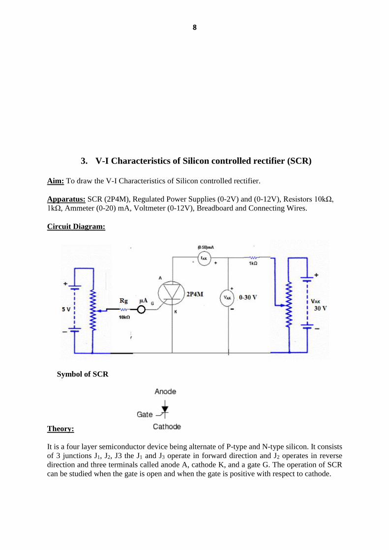
3. V-I Characteristics of Silicon controlled rectifier (SCR)
Aim: To draw the V-I Characteristics of Silicon controlled rectifier.
Apparatus: SCR (2P4M), Regulated Power Supplies (0-2V) and (0-12V), Resistors 10kΩ,
1kΩ, Ammeter (0-20) mA, Voltmeter (0-12V), Breadboard and Connecting Wires.
Circuit Diagram:
Symbol of SCR
Theory:
It is a four layer semiconductor device being alternate of P-type and N-type silicon. It consists
of 3 junctions J1, J2, J3 the J1 and J3 operate in forward direction and J2 operates in reverse
direction and three terminals called anode A, cathode K, and a gate G. The operation of SCR
can be studied when the gate is open and when the gate is positive with respect to cathode.

9
When gate is open, no voltage is applied at the gate due to reverse bias of the junction J2 no
current flows through R2 and hence SCR is at cut off. When anode voltage is increased J2 tends
to breakdown.
When the gate positive, with respect to cathode J3 junction is forward biased and J2 is reverse
biased. Electrons from N-type material move across junction J3 towards gate while holes from
P-type material moves across junction J3 towards cathode. So gate current starts flowing, anode
current increases in extremely small current, junction J2 break down and SCR conducts heavily.
When gate is open the break-over voltage is determined on the minimum forward voltage at
which SCR conducts heavily. Now most of the supply voltage appears across the load
resistance. The holding current is the maximum anode current gate being open, when break
over occurs.
Procedure:
1. Connections are made as per circuit diagram.
2. Keep the gate supply voltage at some constant value
3. Vary the anode to cathode supply voltage and note down the readings of voltmeter
and ammeter. Keep the gate voltage at standard value.
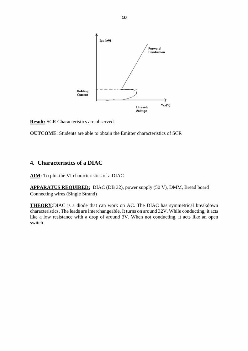
4. A graph is drawn between VAK and IAK.
Observation:
Ig = ( µA)
VAK(V) IAK (mA)
Model Wave form:
Ig = ( µA)
VAK(V) IAK ( mA)
10
Result: SCR Characteristics are observed.
OUTCOME: Students are able to obtain the Emitter characteristics of SCR
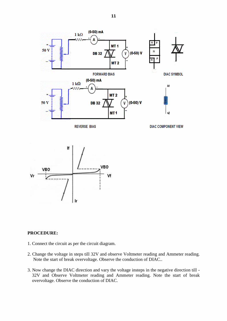
4. Characteristics of a DIAC
AIM: To plot the VI characteristics of a DIAC
APPARATUS REQUIRED: DIAC (DB 32), power supply (50 V), DMM, Bread board
Connecting wires (Single Strand)
THEORY:DIAC is a diode that can work on AC. The DIAC has symmetrical breakdown
characteristics. The leads are interchangeable. It turns on around 32V. While conducting, it acts
like a low resistance with a drop of around 3V. When not conducting, it acts like an open
switch.
11
PROCEDURE:
1. Connect the circuit as per the circuit diagram.
2. Change the voltage in steps till 32V and observe Voltmeter reading and Ammeter reading.
Note the start of break overvoltage. Observe the conduction of DIAC..
3. Now change the DIAC direction and vary the voltage insteps in the negative direction till -
32V and Observe Voltmeter reading and Ammeter reading. Note the start of break
overvoltage. Observe the conduction of DIAC.
12
.4. The characteristics are tabulated and plotted.
OBSERVATIONS:
Forward Characteristics Reverse Characteristics
Vf (V) If (mA) Vr (V) Ir (mA)
RESULT: The VI characteristics of a DIAC have been plotted.
OUTCOME:
Students acquire skill in connecting components using breadboard and connecting
wires to form circuit.
They become able to determine the Emitter characteristics of SCR
5. UJT as a Relaxation Oscillator
Aim: To Study the operation of UJT as a Relaxation Oscillator
Apparatus: UJT (2N2646), CRO (0 – 20 MHz (Dual channel), Function generator 1Hz – 1
MHz, Capacitor (0.1µF), Resistors (100 , 47 , 10 k ), Bread board and connecting wires,
Regulated Power supply 0-12V DC
Circuit diagram:
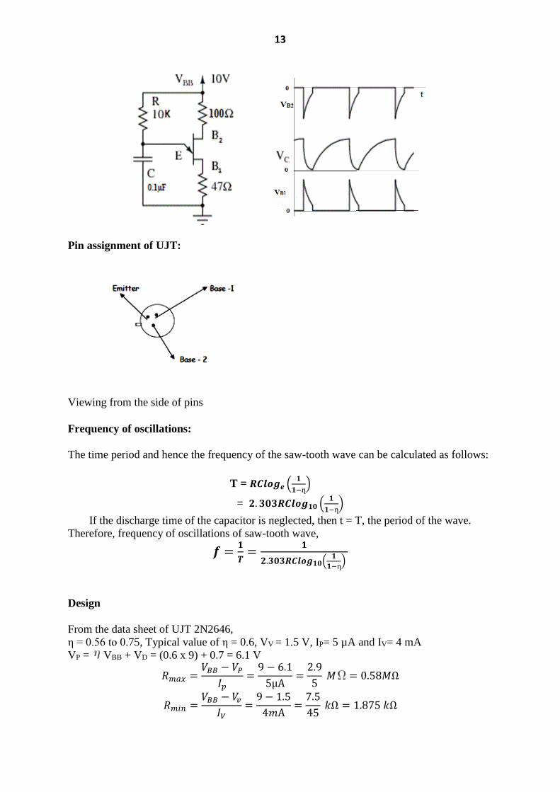
13
Pin assignment of UJT:
Viewing from the side of pins
Frequency of oscillations:
The time period and hence the frequency of the saw-tooth wave can be calculated as follows:
T = 𝑹𝑪𝒍𝒐𝒈𝒆 (𝟏
𝟏−ƞ)
= 𝟐. 𝟑𝟎𝟑𝑹𝑪𝒍𝒐𝒈𝟏𝟎 (𝟏
𝟏−ƞ)
If the discharge time of the capacitor is neglected, then t = T, the period of the wave.
Therefore, frequency of oscillations of saw-tooth wave,
𝒇 =𝟏
𝑻=
𝟏
𝟐.𝟑𝟎𝟑𝑹𝑪𝒍𝒐𝒈𝟏𝟎(𝟏
𝟏−ƞ)
Design
From the data sheet of UJT 2N2646,
η = 0.56 to 0.75, Typical value of η = 0.6, VV = 1.5 V, IP= 5 µA and IV= 4 mA
VP = VBB + VD = (0.6 x 9) + 0.7 = 6.1 V
𝑅𝑚𝑎𝑥 =𝑉𝐵𝐵 − 𝑉𝑃
𝐼𝑝=
9 − 6.1
5µA=
2.9
5 𝑀 = 0.58𝑀Ω
𝑅𝑚𝑖𝑛 =𝑉𝐵𝐵 − 𝑉𝑣
𝐼𝑉=
9 − 1.5
4𝑚A=
7.5
45 𝑘Ω = 1.875 𝑘Ω

14
Taking geometric mean,
𝑅 = √𝑅𝑚𝑎𝑥 × 𝑅𝑚𝑖𝑛 = √(0.58𝑀Ω × 1.875 𝑘Ω) = 32.76 k
Select, R= 33 kΩ. For convenience select R= 10 kΩ
Let the required frequency be 1 kHz, then T=1/f =10-3s.
T = 𝑅𝐶𝑙𝑜𝑔𝑒 (1
1−ƞ)
10-3s = 10x103xC 𝑙𝑜𝑔𝑒 (1
1−0.6)
𝐶 = 10−7
𝑙𝑜𝑔𝑒(1
1−0.6)
= 10−7
0.9163= 0.1µF
Procedure:
1. Connect the circuit as shown in figure.
2. Apply 10 V DC power supply to the circuit.
3. Observe the output waveform on the CRO at B1, B2 and VO and Plot the graphs
4. Vary the time constant (RC) by varying capacitor (C) or potentiometer (R) and
observe the variations in the output pulses on the CRO at B1, B2 and VO.
Result:
UJT relaxation oscillator is constructed and output waveforms are obtained.
Frequency of oscillations = -------Hz.
Outcome:
After finishing this experiment students are able to understand the operation of UJT as
a relaxation oscillator.
Students become able to design a relaxation oscillator
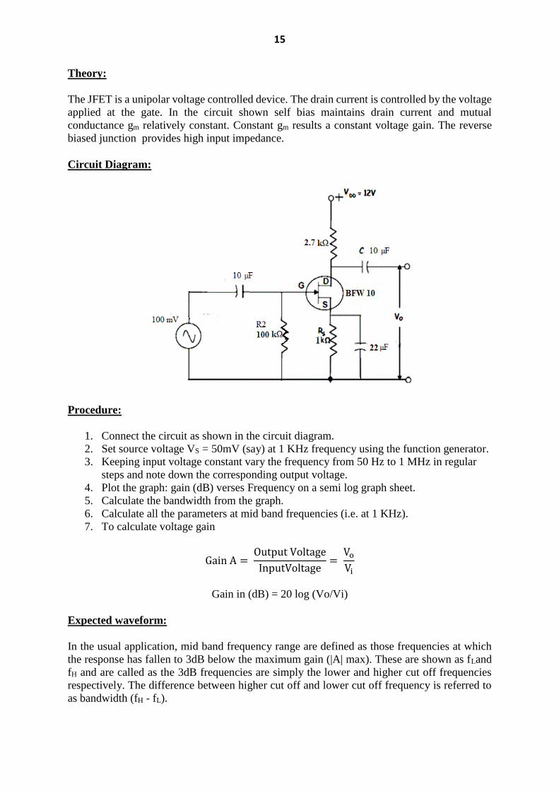
6. JFET common source amplifier
Aim:
To study the JFET common source amplifier and find it’s cut off frequencies and Bandwidth.
Components: JFET BFW 10, Resistor 2.7K , 1.0 K , 100 K , Capacitor 10µF, 22µF,
Bread Board, power supply, Function Generator, Connecting Wires.
15
Theory:
The JFET is a unipolar voltage controlled device. The drain current is controlled by the voltage
applied at the gate. In the circuit shown self bias maintains drain current and mutual
conductance gm relatively constant. Constant gm results a constant voltage gain. The reverse
biased junction provides high input impedance.
Circuit Diagram:
Procedure:
1. Connect the circuit as shown in the circuit diagram.
2. Set source voltage VS = 50mV (say) at 1 KHz frequency using the function generator.
3. Keeping input voltage constant vary the frequency from 50 Hz to 1 MHz in regular
steps and note down the corresponding output voltage.
4. Plot the graph: gain (dB) verses Frequency on a semi log graph sheet.
5. Calculate the bandwidth from the graph.
6. Calculate all the parameters at mid band frequencies (i.e. at 1 KHz).
7. To calculate voltage gain
Gain A = Output Voltage
InputVoltage=
Vo
Vi
Gain in (dB) = 20 log (Vo/Vi)
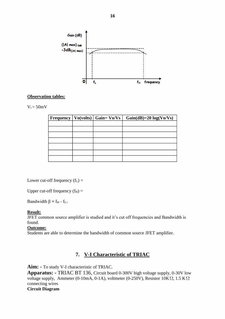
Expected waveform:
In the usual application, mid band frequency range are defined as those frequencies at which
the response has fallen to 3dB below the maximum gain (|A| max). These are shown as fLand
fH and are called as the 3dB frequencies are simply the lower and higher cut off frequencies
respectively. The difference between higher cut off and lower cut off frequency is referred to
as bandwidth (fH - fL).
16
Observation tables:
Vi = 50mV
Frequency Vo(volts) Gain= Vo/Vs Gain(dB)=20 log(Vo/Vs)
Lower cut-off frequency (fL) =
Upper cut-off frequency (fH) =
Bandwidth β = fH - fL=
Result: JFET common source amplifier is studied and it’s cut off frequencies and Bandwidth is
found.
Outcome:
Students are able to determine the bandwidth of common source JFET amplifier.
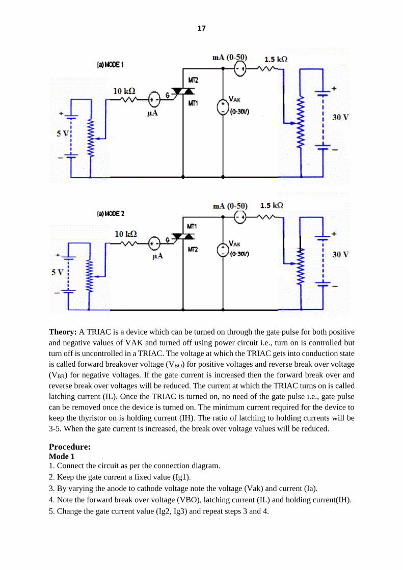
7. V-I Characteristic of TRIAC
Aim: - To study V-I characteristic of TRIAC.
Apparatus: - TRIAC BT 136, Circuit board 0-300V high voltage supply, 0-30V low
voltage supply, Ammeter (0-10mA, 0-1A), voltmeter (0-250V), Resistor 10K , 1.5 K
connecting wires
Circuit Diagram
17
Theory: A TRIAC is a device which can be turned on through the gate pulse for both positive
and negative values of VAK and turned off using power circuit i.e., turn on is controlled but
turn off is uncontrolled in a TRIAC. The voltage at which the TRIAC gets into conduction state
is called forward breakover voltage (VBO) for positive voltages and reverse break over voltage
(VBR) for negative voltages. If the gate current is increased then the forward break over and
reverse break over voltages will be reduced. The current at which the TRIAC turns on is called
latching current (IL). Once the TRIAC is turned on, no need of the gate pulse i.e., gate pulse
can be removed once the device is turned on. The minimum current required for the device to
keep the thyristor on is holding current (IH). The ratio of latching to holding currents will be
3-5. When the gate current is increased, the break over voltage values will be reduced.
Procedure: Mode 1
1. Connect the circuit as per the connection diagram.
2. Keep the gate current a fixed value (Ig1).
3. By varying the anode to cathode voltage note the voltage (Vak) and current (Ia).
4. Note the forward break over voltage (VBO), latching current (IL) and holding current(IH).
5. Change the gate current value (Ig2, Ig3) and repeat steps 3 and 4.
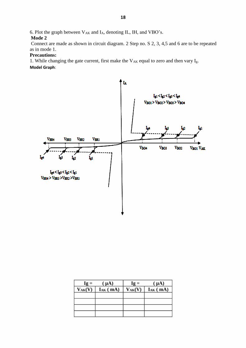
18
6. Plot the graph between VAK and IA, denoting IL, IH, and VBO’s.
Mode 2
Connect are made as shown in circuit diagram. 2 Step no. S 2, 3, 4,5 and 6 are to be repeated
as in mode 1.
Precautions:
1. While changing the gate current, first make the VAK equal to zero and then vary Ig.
Model Graph:
Ig = ( µA) Ig = ( µA)
VAK(V) IAK ( mA) VAK(V) IAK ( mA)

19
Ig = ( µA) Ig = ( µA)
Result:
Characteristics of TRIAC are studied for two different triggering currents.
Outcome
Students are able to understand the working principle of a TRIAC


