Embed Size (px)
Citation preview
Laser-induced Single-bit Faults in Flash Memory:Instructions Corruption on a 32-bit
Microcontroller ?
Brice Colombier∗, Alexandre Menu†, Jean-Max Dutertre†,Pierre-Alain Moëllic∗, Jean-Baptiste Rigaud†,Jean-Luc Danger‡
∗CEA Tech, Centre CMP, Equipe Commune CEA Tech - Mines Saint-Etienne,F-13541 Gardanne France
{brice.colombier, pierre-alain.moellic}@cea.fr;†Mines Saint-Etienne, CEA Tech, Centre CMP, F-13541 Gardanne France
{alexandre.menu, dutertre, rigaud}@emse.fr‡LTCI, Télécom ParisTech , Institut Mines-télécom, Université Paris Saclay,
75634 Paris Cedex 13, [email protected]
Abstract. Physical attacks are a known threat posed against secure em-bedded systems. Notable among these is laser fault injection, which is oftenconsidered as the most effective fault injection technique. Indeed, laserfault injection provides a high spatial accuracy, which enables an attackerto induce bit-level faults. However, experience gained from attacking 8-bittargets might not be relevant on more advanced micro-architectures, andthese attacks become increasingly challenging on 32-bit microcontrollers.In this article, we show that the flash memory area of a 32-bit micro-controller is sensitive to laser fault injection. These faults occur duringthe instruction fetch process, hence the stored value remains unaltered.After a thorough characterisation of the induced faults and the associ-ated fault model, we provide detailed examples of bit-level corruptionof instructions and demonstrate practical applications in compromisingthe security of real-life codes. Based on these experimental results, weformulate a hypothesis about the underlying micro-architectural featuresthat explain the observed fault model.
Keywords: Fault attack, laser injection, flash memory
1 Introduction
Physical attacks pose a considerable threat to the security of embed-ded systems. Provided physical access to a device, an attacker can exploithardware-based vulnerabilities to bypass existing security measures. Among? Part of this work is funded by French ANR program (DS0901/2015) with the projectPROSECCO (ANR-15-CE39-0008)
2 Brice Colombier, Alexandre Menu et al.
these techniques, fault injection consists in disturbing the operating con-ditions of a device, while a secure computation takes place, in order toretrieve secret information or be granted unauthorised privileges. Laserfault injection features a high spatial accuracy, which enables an attacker toinduce single bit-flips in static memory cells of 8-bit [13] and 32-bit micro-controllers [32]. An explanation of the fault mechanism at the architecturallevel was proposed, based on the physical understanding of laser injectionphenomenon [24, 14]. Conversely, this technique is expensive and difficultto carry out with numerous precise parameters to tune, which might resultin endless explorations of the parameters space. While increasing chipintegration enables designers to integrate complex 32-bit architectures,only few work investigate laser injection on these System-on-Chip architec-tures [31, 16, 32, 15]. Besides, none of them address the underlying faultmechanism, which makes it difficult to explain the observed fault modelsin a consistent framework.
In this article, we highlight the flash memory as an area of interest forlaser fault injection on a 32-bit microcontroller. We observe that individualbits of the fetched instructions can be set. The stored value remainsuntouched, only the read value is altered. For example, the data, thesource, or the destination register of the fetched instruction can be altered,but also the opcode itself, potentially changing the instruction itself. Suchmodifications give rise to severe security concerns, since an attacker canthen tamper with the instructions on the fly before they are executed.
The contributions of this article are the following. First, we highlightthe sensitivity of flash memory to the single-bit “bit-set” fault model.We detail the influence of each parameter of the laser on the injectedfault. Then we apply this fault model to real-life codes and show how itundermines their security. Finally, we discuss a physical explanation forthe observed faults, which is consistent with the micro-architecture of theNOR flash memory of our target.
The outline of the article is as follows. In Section 2, we analyse previousworks on laser fault injection, pointing out the current scarcity of resultsand understanding of fault injection on 32-bit microcontrollers. In Section 3,we detail our experimental setup. In Section 4, we describe the obtainedfault model and how it is affected by the parameters of our experimentalsetup. In Section 5, we highlight how the previously described fault modelapplies to implementations of a PIN verification and AES-128 algorithmsby demonstrating two attacks that we performed. In Section 6, we discussa hypothesis on the physical phenomenon accounting for the observed fault
Title Suppressed Due to Excessive Length 3
model, as well as the limitations of our setup. Finally, Section 7 concludesthe article.
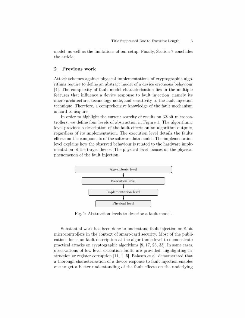
2 Previous work
Attack schemes against physical implementations of cryptographic algo-rithms require to define an abstract model of a device erroneous behaviour[4]. The complexity of fault model characterisation lies in the multiplefeatures that influence a device response to fault injection, namely itsmicro-architecture, technology node, and sensitivity to the fault injectiontechnique. Therefore, a comprehensive knowledge of the fault mechanismis hard to acquire.
In order to highlight the current scarcity of results on 32-bit microcon-trollers, we define four levels of abstraction in Figure 1. The algorithmiclevel provides a description of the fault effects on an algorithm outputs,regardless of its implementation. The execution level details the faultseffects on the components of the software data model. The implementationlevel explains how the observed behaviour is related to the hardware imple-mentation of the target device. The physical level focuses on the physicalphenomenon of the fault injection.
Algorithmic level
Execution level
Implementation level
Physical level
Fig. 1: Abstraction levels to describe a fault model.
Substantial work has been done to understand fault injection on 8-bitmicrocontrollers in the context of smart-card security. Most of the publi-cations focus on fault description at the algorithmic level to demonstratepractical attacks on cryptographic algorithms [8, 17, 25, 33]. In some cases,observations of low-level execution faults are provided, highlighting in-struction or register corruption [11, 1, 5]. Balasch et al. demonstrated thata thorough characterisation of a device response to fault injection enablesone to get a better understanding of the fault effects on the underlying
4 Brice Colombier, Alexandre Menu et al.
hardware implementation [1]. At the same time, several authors observedthat timing constraints violation could explain the observed fault modelsat the physical level [26, 19]. While none of these works addressed all fourlevels of abstraction, they reflect a global understanding of fault injectionon 8-bit microcontrollers.
Current work on 32-bit architectures follows a similar timeline. Most ofthe publications focus so far on empirical observations at the algorithmic [6]and execution level [31, 30]. However, the observed fault models lack a con-sistent framework. Several difficulties can be underlined while attemptingto understand the effect of fault injection on 32-bit architectures.
First, advanced technology nodes enable designers to improve theperformance of a chip with architectural features like pipeline and cachemechanisms. They greatly increase the complexity of black-box fault effectsanalysis [20, 22] as already observed on 8-bit architectures [1].
Second, fault injection techniques leveraging timing constraints vio-lation fail to catch local features of 32-bit micro-architectures. Indeed,attempts to characterise the effects of clock glitches on 32-bit architecturesobtained very similar results to those with 8-bit architectures [2, 19], whiledifferent fault models were observed with optical injection depending onthe injection locality [15].
Third, substantial work has been done to understand fault effects on32-bit microcontroller at the execution and implementation level usinglocal electromagnetic fault injection [20, 22]. However, chip sensitivity tothe underlying physical phenomenon is not understood yet and lacks aconsistent description [21].
Laser fault injection was introduced by Skorobogatov in 2002, based onrelated works on the simulation of ionising radiation in semiconductors de-vices [29]. Provided access to the die, an attacker can induce electron-holedissociation on the path of a laser beam. As a consequence, a photoelectriccurrent is generated in reverse biased junctions of the illuminated tran-sistors. This effect was investigated to describe the bit-flip fault modelin SRAM cells [24, 14] with attacks on AES encryption [13] and secureprogram register [32]. Both physical understanding and spatial accuracyof laser fault injection make this technique well suited to gain insight intothe effects of fault injection on 32-bit architecture.
Previous work on flash memory vulnerabilities pointed out the memorycontrol logic as a sensitive area to laser fault injection [27, 28, 7] althoughthe authors do not explain the underlying fault mechanism.
In this article, we characterise the effect of laser injection in the flashmemory area and observe that single bit-set in data fetched from the
Title Suppressed Due to Excessive Length 5
flash memory can be performed. We then give several examples of instruc-tions corruption. We demonstrate the validity of the fault model on theimplementations of two security algorithms in Section 5 and propose atransistor-level explanation of the physical fault mechanism in Section 6.
3 Methods and experimental setup
3.1 Target board and microcontroller
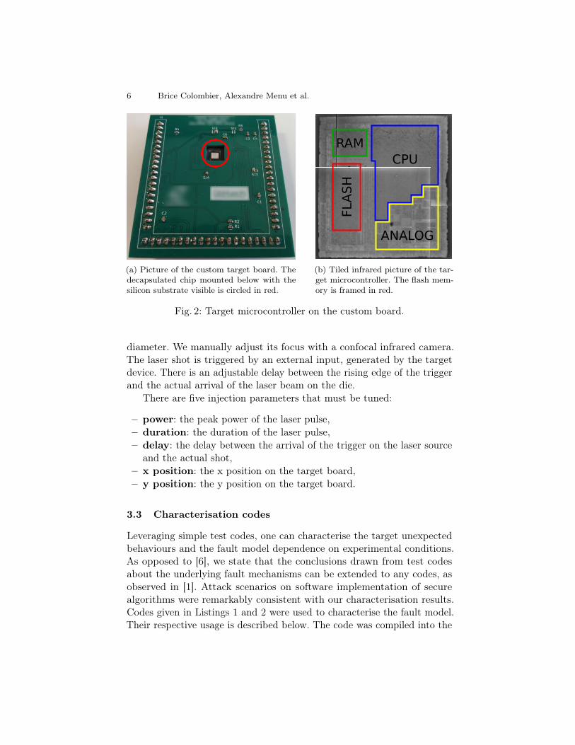
The target microcontroller that we used for our experiments embeds anARM Cortex-M3 core with 128 kB of flash memory and is manufactured atthe 90 nm technology node. It is mounted on a ChipWhisperer [9] targetboard, with the chip soldered below and facing up. We designed a customtarget board suitable for laser injection thanks to the open-source hard-ware information provided for the ChipWhisperer platform1. The targetmicrocontroller runs at the 7.4MHz frequency fixed by the ChipWhispererplatform, corresponding to a 135 ns clock period. An opening was cut onthe PCB board, just under the chip, to give access to its back-side.
To perform laser fault injection, the back of the chip must be de-capsulated to show the silicon substrate. This is performed by chemicalprocessing before the chip is mounted on the board. The decapsulationmust be carried out with great care, especially regarding the amount ofchemical product used to decapsulate: too few keeps part of the die covered,thereby reducing the fault injection area, too much makes the decapsulatedchip very fragile. Thinning the die was not necessary here. A picture ofthe board is shown in Figure 2. This target board is then mounted on theChipWhisperer motherboard and put in place on the laser bench.
3.2 Laser characteristics and parameters
The laser source uses an acousto-optic technology to generate an infraredlaser beam at a wavelength of 1,064 nm. An infrared laser is a necessity toperform fault injection through the back-side since the silicon substrate isopaque to visible light. An infrared laser can go through it and impact theactive regions of the transistors.
The laser source can shoot laser pulses as short as 50 ns with a maximumpower of 3W. The laser pulse is directed to the focusing system by anoptical fiber. The focusing system allows to obtain a laser spot of 5 µm in1 https://github.com/newaetech/chipwhisperer/tree/develop/hardware/victims/cw308_ufo_target
6 Brice Colombier, Alexandre Menu et al.
(a) Picture of the custom target board. Thedecapsulated chip mounted below with thesilicon substrate visible is circled in red.
RAMCPU
ANALOG
FLASH
(b) Tiled infrared picture of the tar-get microcontroller. The flash mem-ory is framed in red.
Fig. 2: Target microcontroller on the custom board.
diameter. We manually adjust its focus with a confocal infrared camera.The laser shot is triggered by an external input, generated by the targetdevice. There is an adjustable delay between the rising edge of the triggerand the actual arrival of the laser beam on the die.
There are five injection parameters that must be tuned:
– power: the peak power of the laser pulse,– duration: the duration of the laser pulse,– delay: the delay between the arrival of the trigger on the laser source
and the actual shot,– x position: the x position on the target board,– y position: the y position on the target board.
3.3 Characterisation codes
Leveraging simple test codes, one can characterise the target unexpectedbehaviours and the fault model dependence on experimental conditions.As opposed to [6], we state that the conclusions drawn from test codesabout the underlying fault mechanisms can be extended to any codes, asobserved in [1]. Attack scenarios on software implementation of securealgorithms were remarkably consistent with our characterisation results.Codes given in Listings 1 and 2 were used to characterise the fault model.Their respective usage is described below. The code was compiled into the
Title Suppressed Due to Excessive Length 7
Thumb instruction set. Therefore, instructions can either be 16 or 32-bitwide and are sometimes unaligned. Data stored in flash memory is said tobe aligned if it is stored at an address which is a multiple of 32 bits.
Bit-level characterisation of fault location The first code highlightsmodifications in data fetched from flash memory. The target instruction ison line 4 of Listing 1.
Listing 1 Characterisation of bit-set location.1 test_data:2 .word 0x000000003 NOP4 LDR R0, test_data5 NOP6 # Reading back R0
This LDR instruction fetches the 32-bit word 0x00000000 stored at thetest_data label and stores it in register R0. A fault is detected on the thirdbit if, for instance, the actual value stored in register R0 is 0x00000008after a laser injection was performed. The test word 0x00000000 was usedto highlight bit-sets, as prior test with the word 0xFFFFFFFF validatedthat we were not able to induce bit-resets. The advantage of faulting rawdata instead of an instruction is that it allows to observe bit-sets on awhole 32-bit word, whereas a 32-bit instruction always contains several1s, for which the bit-set is not observable. The LDR instruction executesin two clock cycles. In the first clock cycle, the offset of the address atwhich the data is stored is computed. In the second clock cycle, the datais actually read and stored in R0. The second clock cycle is the one wetarget. Dummy instructions (NOP) are inserted before and after the targetinstruction to prevent the effects of instruction corruption on the observedfault model.
Characterisation of fault sensitivity over time The second char-acterisation code aims at highlighting the most fault-sensitive momentsin the execution of instructions. For this, after finding out the locationwhere a given bit can be faulted thanks to the code given in Listing 1,we swept over the injection delay with a 10 ns step to target consecutiveinstructions shown in Listing 2, from line 3 to 9. Under normal conditions,
8 Brice Colombier, Alexandre Menu et al.
Listing 2 Characterisation of sensitivity over time.1 # Initialising registers R0, R1, R4, R5, R6,2 # R8 and R9 to 0xFFFFFFFF3 MOVW R0, 0x00004 MOVW R1, 0x00005 MOVW R4, 0x00006 MOVW R5, 0x00007 MOVW R6, 0x00008 MOVW R8, 0x00009 MOVW R9, 0x0000
10 # Reading back the registers
after executing the code shown in Listing 2, the output consists in several32-bit 0x0000FFFF values stored in registers R0, R1, R4, R5, R6, R8, and R9.
The results obtained with these codes are given in the next section,where we present the influence of the laser parameters on the fault injectionprocess.
4 Observable fault model
4.1 Parameters and types of faults
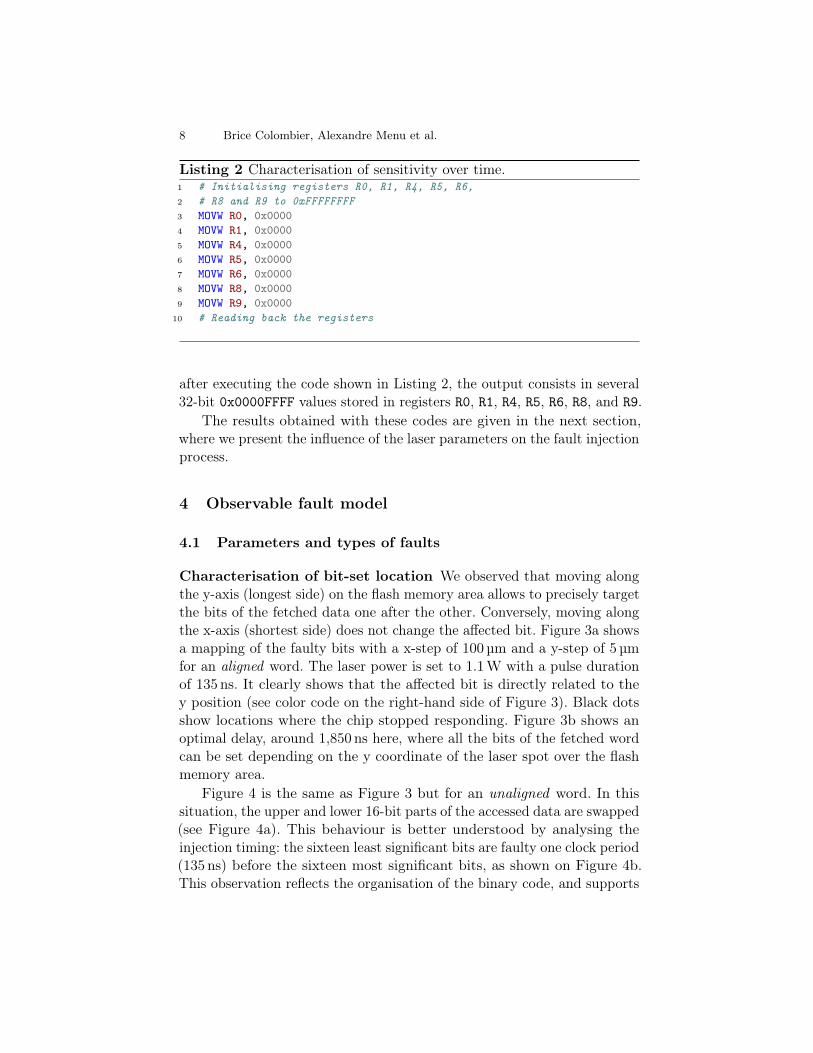
Characterisation of bit-set location We observed that moving alongthe y-axis (longest side) on the flash memory area allows to precisely targetthe bits of the fetched data one after the other. Conversely, moving alongthe x-axis (shortest side) does not change the affected bit. Figure 3a showsa mapping of the faulty bits with a x-step of 100µm and a y-step of 5 µmfor an aligned word. The laser power is set to 1.1W with a pulse durationof 135 ns. It clearly shows that the affected bit is directly related to they position (see color code on the right-hand side of Figure 3). Black dotsshow locations where the chip stopped responding. Figure 3b shows anoptimal delay, around 1,850 ns here, where all the bits of the fetched wordcan be set depending on the y coordinate of the laser spot over the flashmemory area.
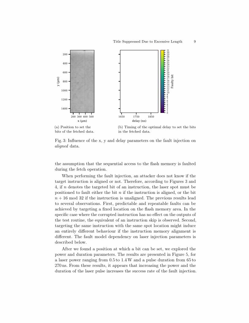
Figure 4 is the same as Figure 3 but for an unaligned word. In thissituation, the upper and lower 16-bit parts of the accessed data are swapped(see Figure 4a). This behaviour is better understood by analysing theinjection timing: the sixteen least significant bits are faulty one clock period(135 ns) before the sixteen most significant bits, as shown on Figure 4b.This observation reflects the organisation of the binary code, and supports
Title Suppressed Due to Excessive Length 9
200 300 400 500x (µm)
200
400
600
800
1000
1200
1400
y (µ
m)
(a) Position to set thebits of the fetched data.
1650 1750 1850delay (ns)
012345678910111213141516171819202122232425262728293031
Faul
ty b
it
(b) Timing of the optimal delay to set the bitsin the fetched data.
Fig. 3: Influence of the x, y and delay parameters on the fault injection onaligned data.
the assumption that the sequential access to the flash memory is faultedduring the fetch operation.
When performing the fault injection, an attacker does not know if thetarget instruction is aligned or not. Therefore, according to Figures 3 and4, if n denotes the targeted bit of an instruction, the laser spot must bepositioned to fault either the bit n if the instruction is aligned, or the bitn+ 16 mod 32 if the instruction is unaligned. The previous results leadto several observations. First, predictable and repeatable faults can beachieved by targeting a fixed location on the flash memory area. In thespecific case where the corrupted instruction has no effect on the outputs ofthe test routine, the equivalent of an instruction skip is observed. Second,targeting the same instruction with the same spot location might inducean entirely different behaviour if the instruction memory alignment isdifferent. The fault model dependency on laser injection parameters isdescribed below.
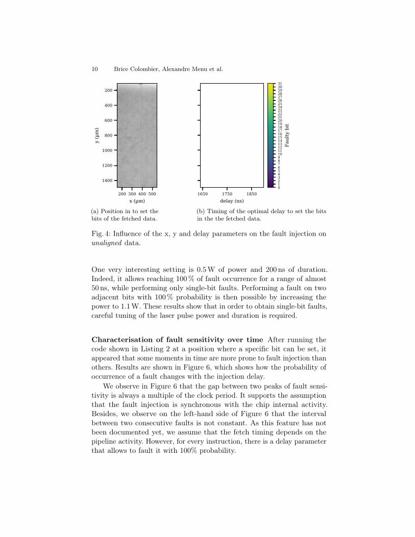
After we found a position at which a bit can be set, we explored thepower and duration parameters. The results are presented in Figure 5, fora laser power ranging from 0.5 to 1.4W and a pulse duration from 65 to270 ns. From these results, it appears that increasing the power and theduration of the laser pulse increases the success rate of the fault injection.
10 Brice Colombier, Alexandre Menu et al.
200 300 400 500x (µm)
200
400
600
800
1000
1200
1400
y (µ
m)
(a) Position in to set thebits of the fetched data.
1650 1750 1850delay (ns)
012345678910111213141516171819202122232425262728293031
Faul
ty b
it
(b) Timing of the optimal delay to set the bitsin the the fetched data.
Fig. 4: Influence of the x, y and delay parameters on the fault injection onunaligned data.
One very interesting setting is 0.5W of power and 200 ns of duration.Indeed, it allows reaching 100% of fault occurrence for a range of almost50 ns, while performing only single-bit faults. Performing a fault on twoadjacent bits with 100% probability is then possible by increasing thepower to 1.1W. These results show that in order to obtain single-bit faults,careful tuning of the laser pulse power and duration is required.
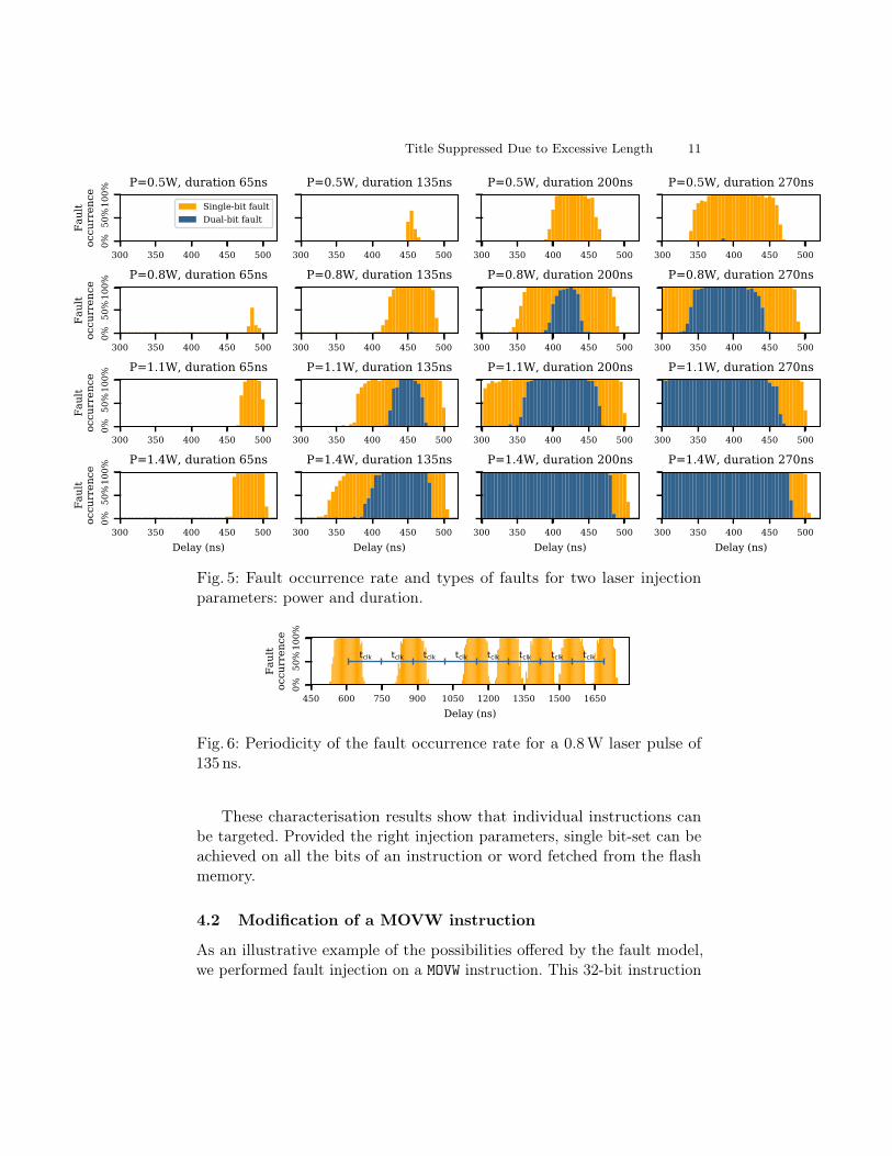
Characterisation of fault sensitivity over time After running thecode shown in Listing 2 at a position where a specific bit can be set, itappeared that some moments in time are more prone to fault injection thanothers. Results are shown in Figure 6, which shows how the probability ofoccurrence of a fault changes with the injection delay.
We observe in Figure 6 that the gap between two peaks of fault sensi-tivity is always a multiple of the clock period. It supports the assumptionthat the fault injection is synchronous with the chip internal activity.Besides, we observe on the left-hand side of Figure 6 that the intervalbetween two consecutive faults is not constant. As this feature has notbeen documented yet, we assume that the fetch timing depends on thepipeline activity. However, for every instruction, there is a delay parameterthat allows to fault it with 100% probability.
Title Suppressed Due to Excessive Length 11
300 350 400 450 500
0%50
%10
0%
Faul
toc
curr
ence
P=0.5W, duration 65ns
Single-bit faultDual-bit fault
300 350 400 450 500
P=0.5W, duration 135ns
300 350 400 450 500
P=0.5W, duration 200ns
300 350 400 450 500
P=0.5W, duration 270ns
300 350 400 450 500
0%50
%10
0%
Faul
toc
curr
ence
P=0.8W, duration 65ns
300 350 400 450 500
P=0.8W, duration 135ns
300 350 400 450 500
P=0.8W, duration 200ns
300 350 400 450 500
P=0.8W, duration 270ns
300 350 400 450 500
0%50
%10
0%
Faul
toc
curr
ence
P=1.1W, duration 65ns
300 350 400 450 500
P=1.1W, duration 135ns
300 350 400 450 500
P=1.1W, duration 200ns
300 350 400 450 500
P=1.1W, duration 270ns
300 350 400 450 500Delay (ns)
0%50
%10
0%
Faul
toc
curr
ence
P=1.4W, duration 65ns
300 350 400 450 500Delay (ns)
P=1.4W, duration 135ns
300 350 400 450 500Delay (ns)
P=1.4W, duration 200ns
300 350 400 450 500Delay (ns)
P=1.4W, duration 270ns
Fig. 5: Fault occurrence rate and types of faults for two laser injectionparameters: power and duration.
450 600 750 900 1050 1200 1350 1500 1650Delay (ns)
0%50
%10
0%
Faul
toc
curr
ence
tclk tclk tclk tclk tclk tclk tclk tclk
Fig. 6: Periodicity of the fault occurrence rate for a 0.8W laser pulse of135 ns.
These characterisation results show that individual instructions canbe targeted. Provided the right injection parameters, single bit-set can beachieved on all the bits of an instruction or word fetched from the flashmemory.
4.2 Modification of a MOVW instruction
As an illustrative example of the possibilities offered by the fault model,we performed fault injection on a MOVW instruction. This 32-bit instruction
12 Brice Colombier, Alexandre Menu et al.
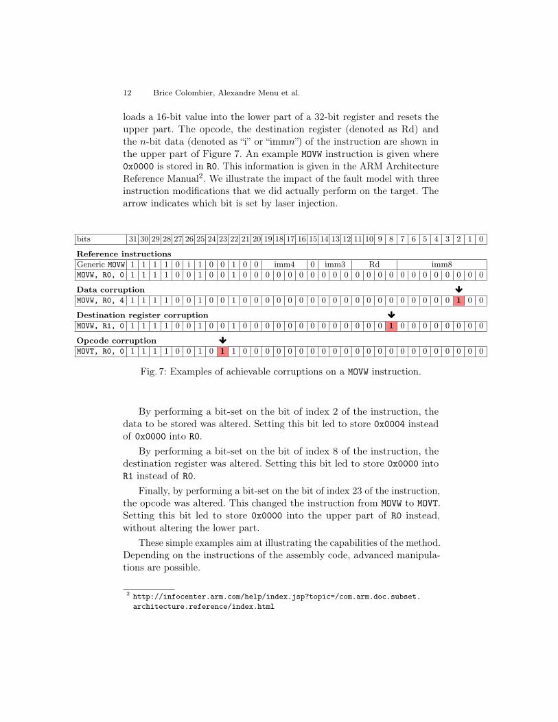
loads a 16-bit value into the lower part of a 32-bit register and resets theupper part. The opcode, the destination register (denoted as Rd) andthe n-bit data (denoted as “i” or “immn”) of the instruction are shown inthe upper part of Figure 7. An example MOVW instruction is given where0x0000 is stored in R0. This information is given in the ARM ArchitectureReference Manual2. We illustrate the impact of the fault model with threeinstruction modifications that we did actually perform on the target. Thearrow indicates which bit is set by laser injection.
bits 31 30 29 28 27 26 25 24 23 22 21 20 19 18 17 16 15 14 13 12 11 10 9 8 7 6 5 4 3 2 1 0
Reference instructionsGeneric MOVW 1 1 1 1 0 i 1 0 0 1 0 0 imm4 0 imm3 Rd imm8MOVW, R0, 0 1 1 1 1 0 0 1 0 0 1 0 0 0 0 0 0 0 0 0 0 0 0 0 0 0 0 0 0 0 0 0 0
Data corruption ø
MOVW, R0, 4 1 1 1 1 0 0 1 0 0 1 0 0 0 0 0 0 0 0 0 0 0 0 0 0 0 0 0 0 0 1 0 0
Destination register corruption ø
MOVW, R1, 0 1 1 1 1 0 0 1 0 0 1 0 0 0 0 0 0 0 0 0 0 0 0 0 1 0 0 0 0 0 0 0 0
Opcode corruption ø
MOVT, R0, 0 1 1 1 1 0 0 1 0 1 1 0 0 0 0 0 0 0 0 0 0 0 0 0 0 0 0 0 0 0 0 0 0
Fig. 7: Examples of achievable corruptions on a MOVW instruction.
By performing a bit-set on the bit of index 2 of the instruction, thedata to be stored was altered. Setting this bit led to store 0x0004 insteadof 0x0000 into R0.
By performing a bit-set on the bit of index 8 of the instruction, thedestination register was altered. Setting this bit led to store 0x0000 intoR1 instead of R0.
Finally, by performing a bit-set on the bit of index 23 of the instruction,the opcode was altered. This changed the instruction from MOVW to MOVT.Setting this bit led to store 0x0000 into the upper part of R0 instead,without altering the lower part.
These simple examples aim at illustrating the capabilities of the method.Depending on the instructions of the assembly code, advanced manipula-tions are possible.
2 http://infocenter.arm.com/help/index.jsp?topic=/com.arm.doc.subset.architecture.reference/index.html
Title Suppressed Due to Excessive Length 13
5 Applications to real-life codes
This section shows how to leverage the fault model described above onreal-life security codes. We did perform all the experiments and obtainedperfect repeatability, in accordance with the fault model described above.It is worth noting that we did not observe any degradation or wear of theFlash memory under attack.
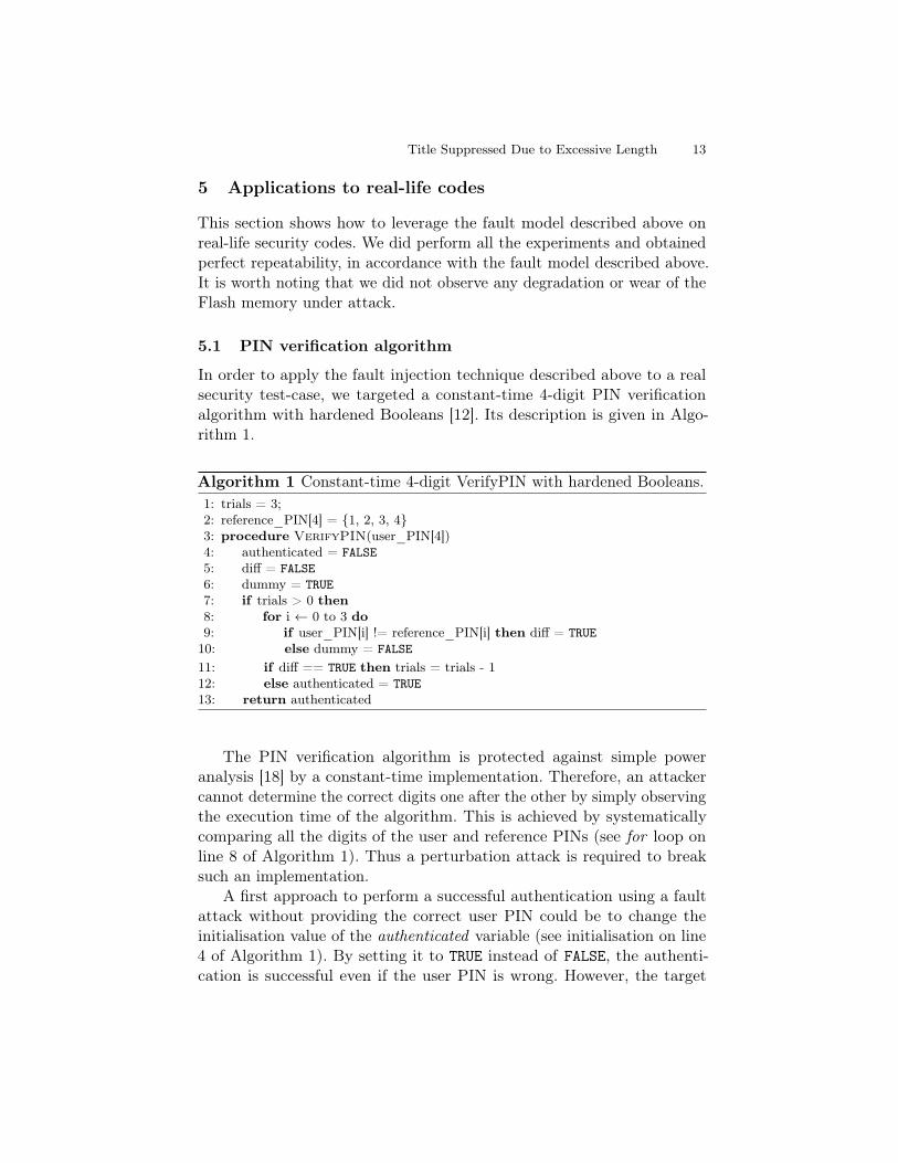
5.1 PIN verification algorithm
In order to apply the fault injection technique described above to a realsecurity test-case, we targeted a constant-time 4-digit PIN verificationalgorithm with hardened Booleans [12]. Its description is given in Algo-rithm 1.
Algorithm 1 Constant-time 4-digit VerifyPIN with hardened Booleans.1: trials = 3;2: reference_PIN[4] = {1, 2, 3, 4}3: procedure VerifyPIN(user_PIN[4])4: authenticated = FALSE5: diff = FALSE6: dummy = TRUE7: if trials > 0 then8: for i ← 0 to 3 do9: if user_PIN[i] != reference_PIN[i] then diff = TRUE10: else dummy = FALSE11: if diff == TRUE then trials = trials - 112: else authenticated = TRUE13: return authenticated
The PIN verification algorithm is protected against simple poweranalysis [18] by a constant-time implementation. Therefore, an attackercannot determine the correct digits one after the other by simply observingthe execution time of the algorithm. This is achieved by systematicallycomparing all the digits of the user and reference PINs (see for loop online 8 of Algorithm 1). Thus a perturbation attack is required to breaksuch an implementation.
A first approach to perform a successful authentication using a faultattack without providing the correct user PIN could be to change theinitialisation value of the authenticated variable (see initialisation on line4 of Algorithm 1). By setting it to TRUE instead of FALSE, the authenti-cation is successful even if the user PIN is wrong. However, the target
14 Brice Colombier, Alexandre Menu et al.
implementation that we used employs hardened Booleans. This commontechnique consists in storing Booleans in bytes and encoding TRUE as 0x55and FALSE as 0xAA for instance. In this case, two bit-sets and two bit-resetsare needed to turn TRUE into FALSE, making the attack very challengingand impractical in our fault injection setup since we can only performbit-sets.
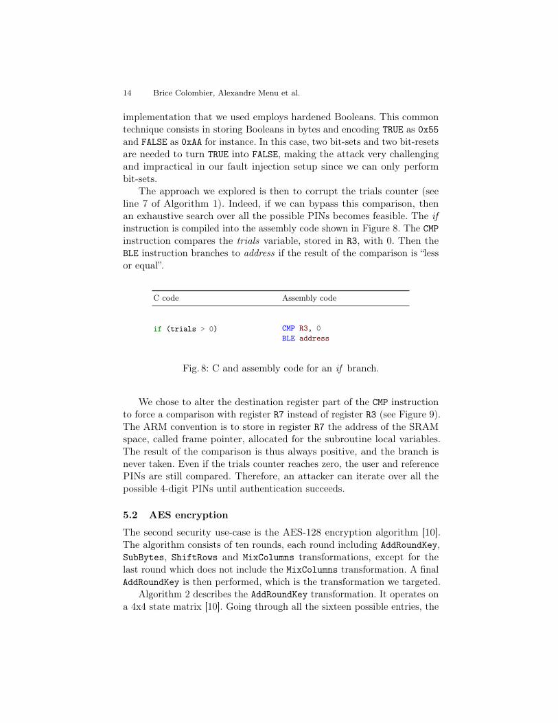
The approach we explored is then to corrupt the trials counter (seeline 7 of Algorithm 1). Indeed, if we can bypass this comparison, thenan exhaustive search over all the possible PINs becomes feasible. The ifinstruction is compiled into the assembly code shown in Figure 8. The CMPinstruction compares the trials variable, stored in R3, with 0. Then theBLE instruction branches to address if the result of the comparison is “lessor equal”.
C code Assembly code
if (trials > 0) CMP R3, 0BLE address
Fig. 8: C and assembly code for an if branch.
We chose to alter the destination register part of the CMP instructionto force a comparison with register R7 instead of register R3 (see Figure 9).The ARM convention is to store in register R7 the address of the SRAMspace, called frame pointer, allocated for the subroutine local variables.The result of the comparison is thus always positive, and the branch isnever taken. Even if the trials counter reaches zero, the user and referencePINs are still compared. Therefore, an attacker can iterate over all thepossible 4-digit PINs until authentication succeeds.
5.2 AES encryption
The second security use-case is the AES-128 encryption algorithm [10].The algorithm consists of ten rounds, each round including AddRoundKey,SubBytes, ShiftRows and MixColumns transformations, except for thelast round which does not include the MixColumns transformation. A finalAddRoundKey is then performed, which is the transformation we targeted.
Algorithm 2 describes the AddRoundKey transformation. It operates ona 4x4 state matrix [10]. Going through all the sixteen possible entries, the
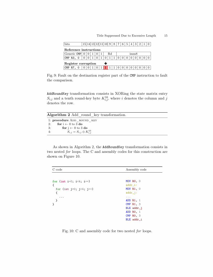
Title Suppressed Due to Excessive Length 15
bits 15 14 13 12 11 10 9 8 7 6 5 4 3 2 1 0
Reference instructionsGeneric CMP 0 0 1 0 1 Rd imm8CMP R3, 0 0 0 1 0 1 0 1 1 0 0 0 0 0 0 0 0
Register corruption ø
CMP R7, 0 0 0 1 0 1 1 1 1 0 0 0 0 0 0 0 0
Fig. 9: Fault on the destination register part of the CMP instruction to faultthe comparison.
AddRoundKey transformation consists in XORing the state matrix entrySi,j and a tenth round-key byte K10
i,j , where i denotes the column and jdenotes the row.
Algorithm 2 Add_round_key transformation.1: procedure Add_round_key2: for i ← 0 to 3 do3: for j ← 0 to 3 do4: Si,j = Si,j ⊕K10
i,j
As shown in Algorithm 2, the AddRoundKey transformation consists intwo nested for loops. The C and assembly codes for this construction areshown on Figure 10.
C code Assembly code
for (int i=0; i<4; i++){
for (int j=0; j<4; j++){
...}
}
MOV R0, 0addr_i:MOV R1, 0addr_j:...ADD R1, 1CMP R1, 3BLE addr_jADD R0, 1CMP R0, 3BLE addr_i
Fig. 10: C and assembly code for two nested for loops.
16 Brice Colombier, Alexandre Menu et al.
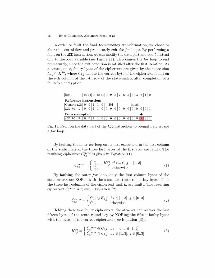
In order to fault the final AddRoundKey transformation, we chose toalter the control flow and prematurely exit the for loops. By performing afault on the ADD instruction, we can modify the data part and add 5 insteadof 1 to the loop variable (see Figure 11). This causes the for loop to endprematurely, since the exit condition is satisfied after the first iteration. Asa consequence, faulty bytes of the ciphertext are given by the expressionCi,j ⊕K10
i,j , where Ci,j denote the correct byte of the ciphertext found onthe i-th column of the j-th row of the state-matrix after completion of afault-free encryption.
bits 15 14 13 12 11 10 9 8 7 6 5 4 3 2 1 0
Reference instructionsGeneric ADD 0 0 1 1 0 Rd imm8ADD R0, 1 0 0 1 1 0 0 0 0 0 0 0 0 0 0 0 1
Data corruption ø
ADD R0, 5 0 0 1 1 0 0 0 0 0 0 0 0 0 1 0 1
Fig. 11: Fault on the data part of the ADD instruction to prematurely escapea for loop.
By faulting the inner for loop on its first execution, in the first columnof the state matrix, the three last bytes of the first row are faulty. Theresulting ciphertext C̃ inner
i,j is given in Equation (1).
C̃ inneri,j =
{Ci,j ⊕K10
i,j if i = 0, j ∈ [1..3]
Ci,j otherwise(1)
By faulting the outer for loop, only the first column bytes of thestate matrix are XORed with the associated tenth round-key bytes. Thusthe three last columns of the ciphertext matrix are faulty. The resultingciphertext C̃outer
i is given in Equation (2).
C̃outeri,j =
{Ci,j ⊕K10
i,j if i ∈ [1..3], j ∈ [0..3]
Ci,j otherwise(2)
Holding these two faulty ciphertexts, the attacker can recover the lastfifteen bytes of the tenth round key by XORing the fifteen faulty byteswith the bytes of the correct ciphertext (see Equation (3)).
K10i,j =
{C̃ inneri,j ⊕ Ci,j if i = 0, j ∈ [1..3]
C̃outeri,j ⊕ Ci,j if i ∈ [1..3], j ∈ [0..3]
(3)
Title Suppressed Due to Excessive Length 17
The first byte of the tenth round key K100,0 must then be brute-forced,
which is easily done in 27 attempts on average. The whole AES key canthen be recovered by reversing the key schedule. To conclude, altering thecontrol-flow of AES encryption and obtaining two faulty ciphertexts allowsan attacker to fully recover the AES key with an average complexity of 27.
6 Discussion
6.1 Possible explanation for the observed fault model
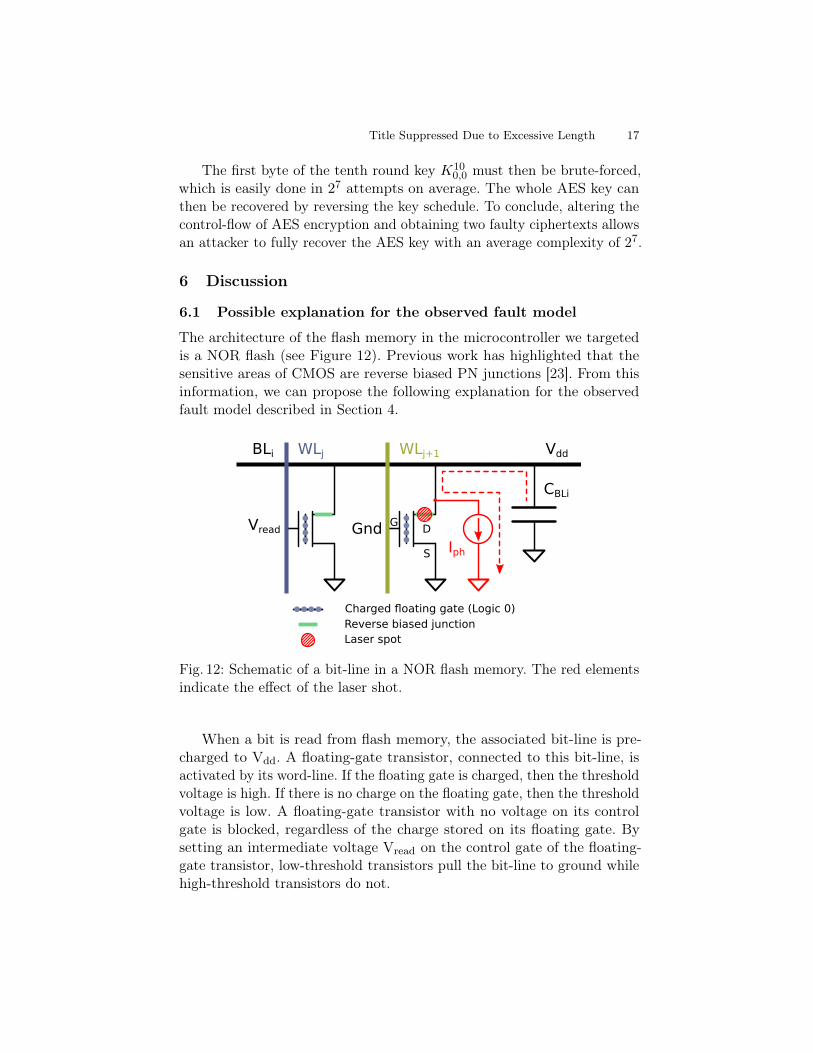
The architecture of the flash memory in the microcontroller we targetedis a NOR flash (see Figure 12). Previous work has highlighted that thesensitive areas of CMOS are reverse biased PN junctions [23]. From thisinformation, we can propose the following explanation for the observedfault model described in Section 4.
D
CBLi
Iph
Vread Gnd
Vdd
G
S
WLj WLj+1BLi
Reverse biased junctionCharged floating gate (Logic 0)
Laser spot
Fig. 12: Schematic of a bit-line in a NOR flash memory. The red elementsindicate the effect of the laser shot.
When a bit is read from flash memory, the associated bit-line is pre-charged to Vdd. A floating-gate transistor, connected to this bit-line, isactivated by its word-line. If the floating gate is charged, then the thresholdvoltage is high. If there is no charge on the floating gate, then the thresholdvoltage is low. A floating-gate transistor with no voltage on its controlgate is blocked, regardless of the charge stored on its floating gate. Bysetting an intermediate voltage Vread on the control gate of the floating-gate transistor, low-threshold transistors pull the bit-line to ground whilehigh-threshold transistors do not.
18 Brice Colombier, Alexandre Menu et al.
In NOR flash memory, floating-gate transistors are connected in parallelbetween a bit-line and the ground. When a laser spot illuminates the drainof a blocked transistor, a photocurrent Iph is induced between its drainand the bulk (connected to ground). This is illustrated by the red elementsin Figure 12. As a consequence, its bit-line is pulled down to ground. Eventhough the word-line activates a floating-gate transistor that stores charges(see left-hand side of Figure 12), then the bit-line would still be pulled toground by the laser-induced photocurrent. There is no physical mechanismto explain how a laser shot could prevent photocurrent from being drawn.Assuming a logic 1 stored in memory is encoded as a low voltage on thebit-line, this explains the asymmetry of the fault model which shows onlybit-sets.
This physical mechanism can be applied to any floating-gate transistorof the flash memory. Assuming that bit-lines are horizontal and word-lines are vertical, it explains why we can sweep over the bits of a fetchedinstruction as we move the laser spot along the y-axis, affecting the bit-linesone after the other. However, moving along the x-axis affects transistorsconnected to the same bit-line, setting the same bit. This explains whymoving along the y-axis allows targeting specific bits, independently ofthe x-coordinate as shown in Figures 3a and 4a.
Finally, the power dependency of the photocurrent spatial distributionexplains why two adjacent bits can be faulted with sufficient power, asshown in Figure 5. By affecting transistors connected to different adjacentbit-lines, adjacent bits can be set.
6.2 Limitations
Mono-spot laser The fact that the laser we use has only one spot limitsthe number of bits that can be simultaneously set in the instruction. Weobserved either a single bit-set or two adjacent bit-sets. A multi-spot lasersetup is thus useful to set multiple non-adjacent bits and extend the rangeof reachable modified instructions.
Bit-set only The observed fault model only consists of bit-sets. We donot observe laser induced bit-reset in this region of the circuit. Even thoughthis limits the range of reachable modified instructions, Section 5 showsthat this fault model has numerous applications.
Control flow corruption mostly As demonstrated by two examplesin Section 5, faulting the control flow of a program is feasible. However,
Title Suppressed Due to Excessive Length 19
given our fault model, faulting the data is impossible most of the timewhile targeting the flash memory. Indeed, data is not hard-coded in theinstructions but instead stored in RAM and fetched when needed. Forexample, it is impossible to perform safe-error attacks on AES encryption[3] since the AES round-key bytes are not hard-coded in the instructions.
Altering the control flow is already an effective way to lower the securityof algorithms though. In future works, some arithmetic operations could bemodified to actually alter the data. However, this is very algorithm-specificand must be investigated for each case.
6.3 Reproducibility with a new target code and an identicalmicrocontroller
Performing extensive characterisation and exploration of laser parametersto perform a correct fault injection is a time-consuming process and cantake months. However, reproducing these results on a new target code andan identical microcontroller would be much faster. It would first requireto decapsulate the chip and mount it on a suitable board for back-sidelaser injection. Then, the code shown in Listing 1 with a laser power of0.5W and duration of 200 ns can be used to find the y coordinates atwhich each individual bit is set. Access to the assembly code of the targetapplication is needed to identify the target instruction. After that, theARM Architecture Reference Manual is used to find out a valid faultyinstruction. Finally, the delay injection parameter must be tuned.
7 Conclusion
This article presented a new laser fault injection attack on the flash memoryof a 32-bit microcontroller. Provided the right injection parameters, anattacker can set individual bits of the words fetched from flash memory in avery predictable manner. Based on our characterisation results, we providedpractical examples of control flow and data corruption affecting commonsecurity algorithms. Finally, we discussed how the hardware features of aNOR flash memory can explain the observed fault model. Future works onthe topic will focus on examining state-of-the-art software countermeasuressuch as control flow integrity that may be relevant against the attacks thatwe demonstrated on the PIN verification and AES algorithms.
20 Brice Colombier, Alexandre Menu et al.
Acknowledgement
The authors would like to thank Colin O’Flynn from NewAE TechnologyInc. for his help in providing the reference designs and bill of materialsfor the custom ChipWhisperer target board. We thank the Micro-PackSplatform too for the PCB design and chip decapsulation.
References
[1] Josep Balasch, Benedikt Gierlichs, and Ingrid Verbauwhede. “An In-depth andBlack-box Characterization of the Effects of Clock Glitches on 8-bit MCUs”. In:Workshop on Fault Diagnosis and Tolerance in Cryptography. 2011, pp. 105–114.
[2] Alessandro Barenghi et al. “Low Voltage Fault Attacks on the RSA Cryptosystem”.In: Workshop on Fault Diagnosis and Tolerance in Cryptography. 2009, pp. 23–31.
[3] Johannes Blömer and Jean-Pierre Seifert. “Fault Based Cryptanalysis of theAdvanced Encryption Standard (AES)”. In: International Conference on FinancialCryptography. Vol. 2742. 2003, pp. 162–181.
[4] Dan Boneh, Richard A. DeMillo, and Richard J. Lipton. “On the Importance ofEliminating Errors in Cryptographic Computations”. In: Journal of Cryptology14.2 (2001), pp. 101–119.
[5] Jakub Breier, Dirmanto Jap, and Chien-Ning Chen. “Laser Profiling for theBack-Side Fault Attacks: With a Practical Laser Skip Instruction Attack on AES”.In: Workshop on Cyber-Physical System Security. 2015, pp. 99–103.
[6] Sebanjila Kevin Bukasa et al. “Let’s shock our IoT’s heart: ARMv7-M under(fault) attacks”. In: International Conference on Availability, Reliability andSecurity. 2018, 33:1–33:6.
[7] Feifei Cai et al. “Optical fault injection attacks for flash memory of smartcards”.In: International Conference on Electronics Information and Emergency Commu-nication. IEEE. 2016, pp. 46–50.
[8] Hamid Choukri and Michael Tunstall. “Round Reduction Using Faults”. In:Workshop on Fault Diagnosis and Tolerance in Cryptography. 2005, pp. 13–24.
[9] Colin O’Flynn and Zhizhang (David) Chen. “ChipWhisperer: An Open-SourcePlatform for Hardware Embedded Security Research”. In: International Workshopon Constructive Side-Channel Analysis and Secure Design. Vol. 8622. 2014,pp. 243–260.
[10] Joan Daemen and Vincent Rijmen. The Design of Rijndael: AES - The AdvancedEncryption Standard. 2002.
[11] Amine Dehbaoui et al. “Electromagnetic Transient Faults Injection on a Hardwareand a Software Implementations of AES”. In: Workshop on Fault Diagnosis andTolerance in Cryptography. 2012, pp. 7–15.
[12] Louis Dureuil et al. “FISSC: A Fault Injection and Simulation Secure Collec-tion”. In: International Conference on Computer Safety, Reliability, and Security.Vol. 9922. 2016, pp. 3–11.
[13] Jean-Max Dutertre et al. “Fault Round Modification Analysis of the advancedencryption standard”. In: International Symposium on Hardware-Oriented Securityand Trust. 2012, pp. 140–145.
[14] Jean-Max Dutertre et al. “Laser fault injection at the CMOS 28 nm technologynode: an analysis of the fault model,” in: FDTC 2018. 2018.
Title Suppressed Due to Excessive Length 21
[15] Oscar M. Guillen, Michael Gruber, and Fabrizio De Santis. “Low-Cost Setup forLocalized Semi-invasive Optical Fault Injection Attacks - How Low Can We Go?”In: International Workshop on Constructive Side-Channel Analysis and SecureDesign. Vol. 10348. 2017, pp. 207–222.
[16] Martin S. Kelly, Keith Mayes, and John F. Walker. “Characterising a CPUfault attack model via run-time data analysis”. In: International Symposium onHardware Oriented Security and Trust. 2017, pp. 79–84.
[17] Chong Hee Kim and Jean-Jacques Quisquater. “Fault Attacks for CRT BasedRSA: New Attacks, New Results, and New Countermeasures”. In: InformationSecurity Theory and Practices. Vol. 4462. 2007, pp. 215–228.
[18] Paul C. Kocher, Joshua Jaffe, and Benjamin Jun. “Differential Power Analysis”.In: Annual International Cryptology Conference. Vol. 1666. 1999, pp. 388–397.
[19] Thomas Korak and Michael Hoefler. “On the Effects of Clock and Power SupplyTampering on Two Microcontroller Platforms”. In: Workshop on Fault Diagnosisand Tolerance in Cryptography. 2014, pp. 8–17.
[20] Nicolas Moro et al. “Electromagnetic Fault Injection: Towards a Fault Modelon a 32-bit Microcontroller”. In: Workshop on Fault Diagnosis and Tolerance inCryptography. 2013, pp. 77–88.
[21] Sébastien Ordas, Ludovic Guillaume-Sage, and Philippe Maurine. “Electromag-netic fault injection: the curse of flip-flops”. In: Journal of Cryptographic Engi-neering 7.3 (2017), pp. 183–197.
[22] Lionel Rivière et al. “High precision fault injections on the instruction cache ofARMv7-M architectures”. In: International Symposium on Hardware OrientedSecurity and Trust. 2015, pp. 62–67.
[23] Cyril Roscian et al. “Fault Model Analysis of Laser-Induced Faults in SRAMMemory Cells”. In: Workshop on Fault Diagnosis and Tolerance in Cryptography.2013, pp. 89–98.
[24] A. Sarafianos et al. “Electrical modeling of the photoelectric effect induced bya pulsed laser applied to an SRAM cell”. In: Microelectronics Reliability 53.9(2013), pp. 1300–1305.
[25] Jörn-Marc Schmidt and Christoph Herbst. “A Practical Fault Attack on Squareand Multiply”. In: International Workshop on Fault Diagnosis and Tolerance inCryptography. 2008, pp. 53–58.
[26] Nidhal Selmane, Sylvain Guilley, and Jean-Luc Danger. “Practical Setup TimeViolation Attacks on AES”. In: European Dependable Computing Conference.2008, pp. 91–96.
[27] Sergei Skorobogatov. “Flash Memory ’Bumping’ Attacks”. In: CryptographicHardware and Embedded Systems. Vol. 6225. 2010, pp. 158–172.
[28] Sergei Skorobogatov. “Optical Fault Masking Attacks”. In: Workshop on FaultDiagnosis and Tolerance in Cryptography. 2010, pp. 23–29.
[29] Sergei P. Skorobogatov and Ross J. Anderson. “Optical Fault Induction Attacks”.In: International Workshop on Cryptographic Hardware and Embedded Systems.Vol. 2523. 2002, pp. 2–12.
[30] Niek Timmers, Albert Spruyt, and Marc Witteman. “Controlling PC on ARMUsing Fault Injection”. In: Workshop on Fault Diagnosis and Tolerance in Cryp-tography. 2016, pp. 25–35.
[31] Elena Trichina and Roman Korkikyan. “Multi Fault Laser Attacks on ProtectedCRT-RSA”. In: Workshop on Fault Diagnosis and Tolerance in Cryptography.2010, pp. 75–86.

22 Brice Colombier, Alexandre Menu et al.
[32] Aurelien Vasselle et al. “Laser-Induced Fault Injection on Smartphone Bypassingthe Secure Boot”. In: Workshop on Fault Diagnosis and Tolerance in Cryptography.2017, pp. 41–48.
[33] Jasper G. J. van Woudenberg, Marc F. Witteman, and Federico Menarini. “Prac-tical Optical Fault Injection on Secure Microcontrollers”. In: Workshop on FaultDiagnosis and Tolerance in Cryptography. 2011, pp. 91–99.