Embed Size (px)
Citation preview
Physical Characterization of Arbiter PUFs
Shahin Tajik1, Enrico Dietz2, Sven Frohmann2, Jean-Pierre Seifert1,Dmitry Nedospasov1, Clemens Helfmeier3, Christian Boit3, Helmar Dittrich2
1Security in Telecommunications, Technische Universitat Berlin, Germany{shahin,jpseifert,dmitry}@sec.t-labs.tu-berlin.de
2Teraherz Spectroscopy, Technische Universitat Berlin, Germany{dietz,sf}@physik.tu-berlin.de
3Semiconductor Devices, Technische Universitat Berlin, Germany{clemens.helfmeier,christian.boit}@tu-berlin.de
Abstract. As intended by its name, Physically Unclonable Functions(PUFs) are considered as an ultimate solution to deal with insecure stor-age, hardware counterfeiting, and many other security problems. How-ever, many different successful attacks have already revealed vulnera-bilities of certain digital intrinsic PUFs. Although settling-state-basedPUFs, such as SRAM PUFs, can be physically cloned by semi-invasiveand fully-invasive attacks, successful attacks on timing-based PUFs wereso far limited to modeling attacks. Such modeling requires a large sub-set of challenge-response-pairs (CRP) to successfully model the targetedPUF. In order to provide a final security answer, this paper proves thatall arbiter-based (i.e. controlled and XOR-enhanced) PUFs can be com-pletely and linearly characterized by means of photonic emission analy-sis. Our experimental setup is capable of measuring every PUF-internaldelay with a resolution of 6 picoseconds. Due to this resolution we in-deed require only the theoretical minimum number of linear independentequations (i.e. physical measurements) to directly solve the underlyinginhomogeneous linear system. Moreover, we neither require to know theactual PUF challenges nor the corresponding PUF responses for ourphysical delay extraction. On top of that devastating result, we are alsoable to further simplify our setup for easier physical measurement han-dling. We present our practical results for a real arbiter PUF implemen-tation on a Complex Programmable Logic Device (CPLD) from Alteramanufactured in a 180 nanometer process.
Keywords: Arbiter PUF, photonic emission analysis, backside, physical characteriza-
tion
1 Introduction
Physically Unclonable Functions (PUFs) offer a promising solution for futuresecurity problems [9]. PUFs can be utilized as the basis for many security ap-plications, such as encryption [13, 29] and hardware fingerprinting [26, 33]. Al-though there are different PUF classifications in the literature regarding their
characteristics, they can generally be categorized in two distinct classes of PUFs:settling-state-based PUFs and timing-based PUFs [15]. The former is based onbistable circuits such as SRAMs, while the latter is based on intrinsic differencesin timing of a set of symmetric circuit paths.
Although unclonability and unpredictability are the main PUF requirements [3,22], previous work in the literature has shown how different PUFs can be attackedand cloned. Settling-state-based PUFs such as SRAM PUFs can be characterizedand cloned physically by semi-invasive and fully invasive attacks [10, 20]. Timing-based PUFs such as Arbiter PUFs are vulnerable to machine-learning attacks,which make it possible to emulate the PUF response [12, 24]. However, machine-learning attacks require a large number of challenge-response pairs (CRP) to pre-dict the response with high probability. Any non-linearity in the PUF responsecan negatively impact the effectiveness of machine-learning techniques [13, 32].As a result substantially more CRPs together with extra side channel informa-tion are required to model the PUF response successfully [16]. However, in areal attack scenario, the intrinsic PUF response may be unavailable to the at-tacker [8, 14]. Moreover, trying a large set of CRPs may also be infeasible dueto other countermeasures implemented on modern secure devices [23].
This work demonstrates that arbiter PUFs and more generally, timing-basedPUFs can be characterized by high-resolution temporal photonic emission anal-ysis from the chip’s backside. This approach does not need any readout of PUFresponse nor does it require a substantial number of challenges to characterizethe PUF. Our methodology is based on measuring the time difference betweenenabling the PUF and photon emission at the output of the last stage. For ourProof-of-concept (PoC), we have implemented an arbiter PUF on a ComplexProgrammable Logic Device (CPLD). The delay between the input of the PUFand the output of photodetector can be measured with an overall resolution ofapproximately 6 picoseconds by a Time-to-Digital Converter (TDC). As a result,the PUF response is determined by comparing the measured delays on both PUFchains. Furthermore, in our methodology, the required challenges for the physicalcharacterization of the PUF increase linearly with PUF length. Finally, based ona mathematical approach we find the minimum number of necessary challengecombinations, which are required to characterize the PUF. Using this method-ology it also possible to characterize controlled PUFs [8], where the challenge isinaccessible to the attacker. As compared to other characterization techniques,such as machine learning, this methodology greatly reduces the amount of mea-surements that are necessary to characterize the intrinsic PUF behavior. Themain contributions of this paper are as follows:
Physical characterization of timing-based PUFs. We present the firstphysical characterization attack on timing-based PUFs with the help of photonicemission analysis. This approach is capable of physically characterizing the in-trinsic behavior of the circuit by measuring the delays within the circuit with ahigh degree of accuracy. In the case of an arbiter PUF this consists of measur-ing the intrinsic delays of each individual stage of the circuit. As compared toother heuristic methodologies which require a substantially greater number of
measurements than individual PUF stages, our methodology requires just twomeasurements per PUF stage.
Low-cost measurement setup for measuring the delay with the res-olution of 6 ps. We introduce an efficient and cost-effective experimental setupwith a substantial temporal resolution. The setup is capable of performing tem-poral measurements with an approximate time resolution of 6 ps. The timeresolution of the setup allows for the exact characterization of the intrinsic de-lays of each individual stage of the PUF. Moreover, the setup provides sufficienttime resolution for modern process nodes.
Practical evaluation against a Proof-of-Concept arbiter PUF imple-mentation. The PoC implementation was realized on a common programmablelogic platform. To extract the device’s intrinsic behavior, we performed dynamicsemi-invasive backside analysis of the photonic emissions of the device. Becausethe analysis techniques are semi-invasive the integrity of the device’s intrinsicresponse is not changedpre.
Mathematical approach for measurement optimization. In order tophysically characterize the PUF, we propose a measurement technique to min-imize the number of challenges that are necessary for a PUF characterization.Furthermore, we provide a mathematical approach for minimizing the effort ofmeasurement for arbiter PUFs in general. Combined, these techniques greatlyreduce the number of measurements and measurement locations that are neces-sary for PUF characterization.
The rest of this paper is organized as follows: Section 2 presents backgroundinformation on the delay-based PUFs and photonic emission in CMOS technol-ogy. Moreover, the programmable logic architecture is explained and the relatedwork is reviewed. In Section 3, the utilized experimental setup is presented. Sec-tion 4 introduces the mathematical approach for the optimized measurement.Section 5 demonstrates the practical results, where we were able to measure thesmall delay differences. In Section 6, we present additional considerations aboutour methodology. Finally in Section 7, we conclude the paper.
2 Background
2.1 Arbiter-based PUF
Due to manufacturing variations, there are small random delay differences onsymmetrical electrical paths on a chip. The entropy of the delays is sufficient toensure a unique PUF response for each individual device instance. Arbiter andRing-oscillator PUFs are two examples of timing-based PUFs [15]. Arbiter PUFsutilize the intrinsic timing differences of two symmetrically designed paths to asingle bit of the response at the output of the circuit [12]. It consists of multipleconnected stages and an arbiter at the end of the chain, see Figure 1. Each stageconsists of two outputs and three inputs, a single bit of the challenge and thetwo outputs from the previous stage. The inputs of the first stage are connectedto a common enable signal. The outputs of the last stage are connected to a so-called arbiter, which determines which signal arrived first. Based on this result,
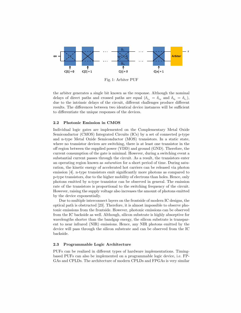
Fig. 1: Arbiter PUF
the arbiter generates a single bit known as the response. Although the nominaldelays of direct paths and crossed paths are equal (δia = δid and δib = δic),due to the intrinsic delays of the circuit, different challenges produce differentresults. The differences between two identical device instances will be sufficientto differentiate the unique responses of the devices.
2.2 Photonic Emission in CMOS
Individual logic gates are implemented on the Complementary Metal OxideSemiconductor (CMOS) Integrated Circuits (ICs) by a set of connected p-typeand n-type Metal Oxide Semiconductor (MOS) transistors. In a static state,where no transistor devices are switching, there is at least one transistor in theoff region between the supplied power (VDD) and ground (GND). Therefore, thecurrent consumption of the gate is minimal. However, during a switching event asubstantial current passes through the circuit. As a result, the transistors enteran operating region known as saturation for a short period of time. During satu-ration, the kinetic energy of accelerated hot carriers can be released via photonemission [4]. n-type transistors emit significantly more photons as compared top-type transistors, due to the higher mobility of electrons than holes. Hence, onlyphotons emitted by n-type transistor can be observed in general. The emissionrate of the transistors is proportional to the switching frequency of the circuit.However, raising the supply voltage also increases the amount of photons emittedby the device exponentially.
Due to multiple interconnect layers on the frontside of modern IC designs, theoptical path is obstructed [23]. Therefore, it is almost impossible to observe pho-tonic emissions from the frontside. However, photonic emissions can be observedfrom the IC backside as well. Although, silicon substrate is highly absorptive forwavelengths shorter than the bandgap energy, the silicon substrate is transpar-ent to near infrared (NIR) emissions. Hence, any NIR photons emitted by thedevice will pass through the silicon substrate and can be observed from the ICbackside.
2.3 Programmable Logic Architecture
PUFs can be realized in different types of hardware implementations. Timing-based PUFs can also be implemented on a programmable logic device, i.e. FP-GAs and CPLDs. The architecture of modern CPLDs and FPGAs is very similar
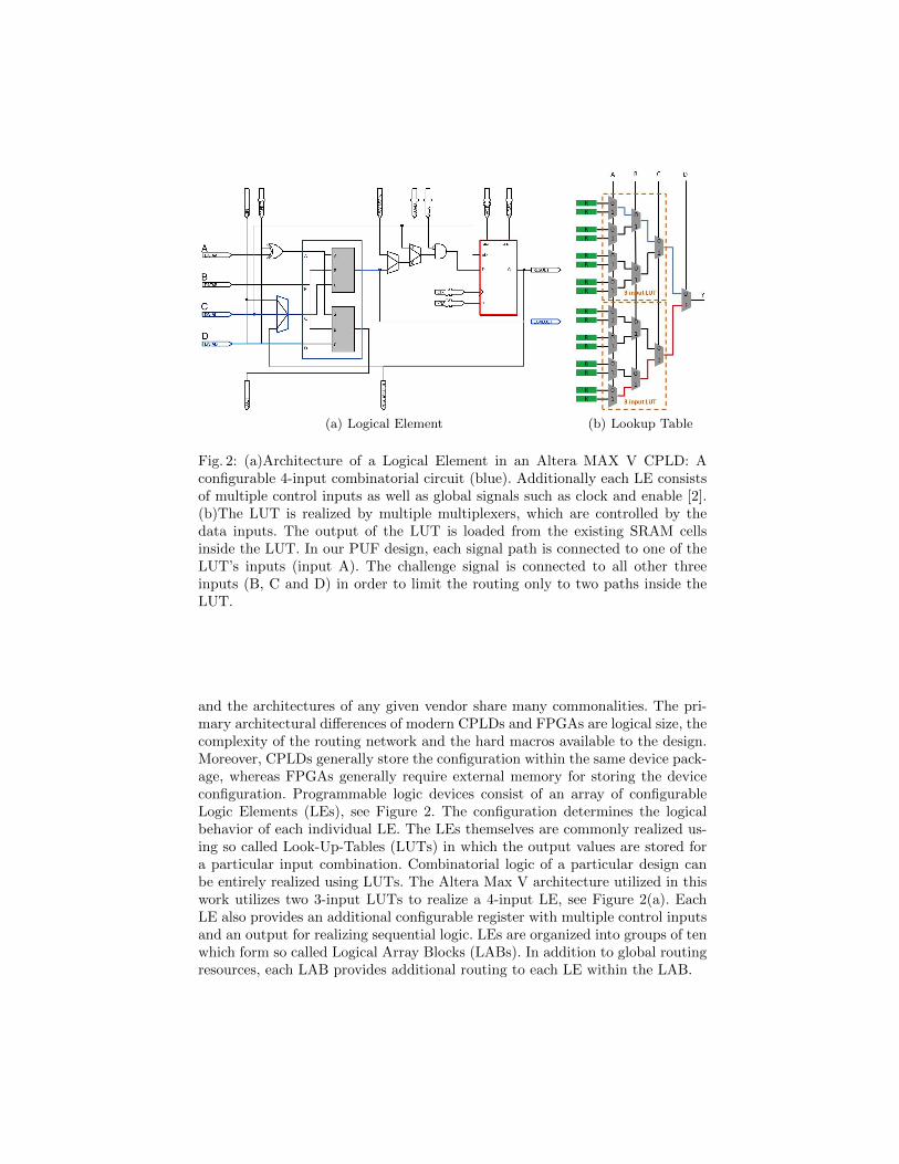
(a) Logical Element (b) Lookup Table
Fig. 2: (a)Architecture of a Logical Element in an Altera MAX V CPLD: Aconfigurable 4-input combinatorial circuit (blue). Additionally each LE consistsof multiple control inputs as well as global signals such as clock and enable [2].(b)The LUT is realized by multiple multiplexers, which are controlled by thedata inputs. The output of the LUT is loaded from the existing SRAM cellsinside the LUT. In our PUF design, each signal path is connected to one of theLUT’s inputs (input A). The challenge signal is connected to all other threeinputs (B, C and D) in order to limit the routing only to two paths inside theLUT.
and the architectures of any given vendor share many commonalities. The pri-mary architectural differences of modern CPLDs and FPGAs are logical size, thecomplexity of the routing network and the hard macros available to the design.Moreover, CPLDs generally store the configuration within the same device pack-age, whereas FPGAs generally require external memory for storing the deviceconfiguration. Programmable logic devices consist of an array of configurableLogic Elements (LEs), see Figure 2. The configuration determines the logicalbehavior of each individual LE. The LEs themselves are commonly realized us-ing so called Look-Up-Tables (LUTs) in which the output values are stored fora particular input combination. Combinatorial logic of a particular design canbe entirely realized using LUTs. The Altera Max V architecture utilized in thiswork utilizes two 3-input LUTs to realize a 4-input LE, see Figure 2(a). EachLE also provides an additional configurable register with multiple control inputsand an output for realizing sequential logic. LEs are organized into groups of tenwhich form so called Logical Array Blocks (LABs). In addition to global routingresources, each LAB provides additional routing to each LE within the LAB.
2.4 Related Work
In recent years, many different attacks on PUFs have been proposed. Settling-state based PUFs, such as SRAM PUFs, can be physically cloned by semi-invasive attacks [10]. The authors of this work demonstrated how SRAM PUFresponses can be characterized by a Focused Ion Beam (FIB) circuit edit. More-over, SRAM PUFs are also vulnerable to fully-invasive attacks, due to lack oftamper detection mechanism [20]. It was also shown that timing-based PUFs,such as Ring-oscillator PUFs, are also vulnerable to semi-invasive electromag-netic (EM) side channel attacks [18].
However, to this date, arbiter PUFs are only the target of mathematicalmodeling attacks. Modeling attacks require a subset of CRPs to build a modelon that and predict the PUF response for all possible challenges [12]. One of thefirst utilized modeling techniques was linear programming to model the timing-based PUF [21]. Machine-learning tools such as Logistic Regression (LR) canalso be utilized to model the arbiter PUF successfully [24]. The modeling attacksbecomes more difficult by introducing non-linearities to the PUF delays and re-sponses. Two example of non-linear PUFs are Feed-forward arbiter PUFs [13]and XOR-PUFs [32]. However, it has been shown that Feed-forward PUFs arevulnerable to evolutionary algorithm [25]. Moreover, a modeling attack basedon higher number of CRPs and power side channel information can be appliedsuccessfully to XOR-arbiter PUFs [16]. Other modeling techniques include solv-ing integer equations utilize the CMOS noise as a side channel information orenvironmental changes as a fault injection technique to model the timing-basedPUFs [6, 5].
Photonic emission analysis is introduced as a new side channel attack toanalyze security applications on the chip such as cryptographic ciphers [7]. Inorder to bypass the multiple interconnect layers on the frontside of the chip,photonic emission analysis and photonic fault injection attacks can be conductedfrom the backside [31, 30]. It has been shown that chips, such as microcontrollers,can be functionally analyzed by their optical emissions during runtime [19].Simple Photonic Emission Analysis (SPEA) is another approach that can recoverthe full AES secret key by monitoring access to S-Box [28]. Furthermore, thefull AES secret key can be recovered by a similar approach called DifferentialPhotonic Emission Analysis [11].
3 Experimental Setup
3.1 Measurement Setup
The experimental setup, shown schematically in Figure 3, is an optimized in-frared microscope equipped with a scientific Si-CCD camera and an InGaAsavalanche diode as detectors for spatial and temporal analysis [27]. The Si-CCDis a back illuminated deep depletion type featuring high quantum efficiency inthe NIR region. To minimize dark current it is cooled down to −70 ◦C, which
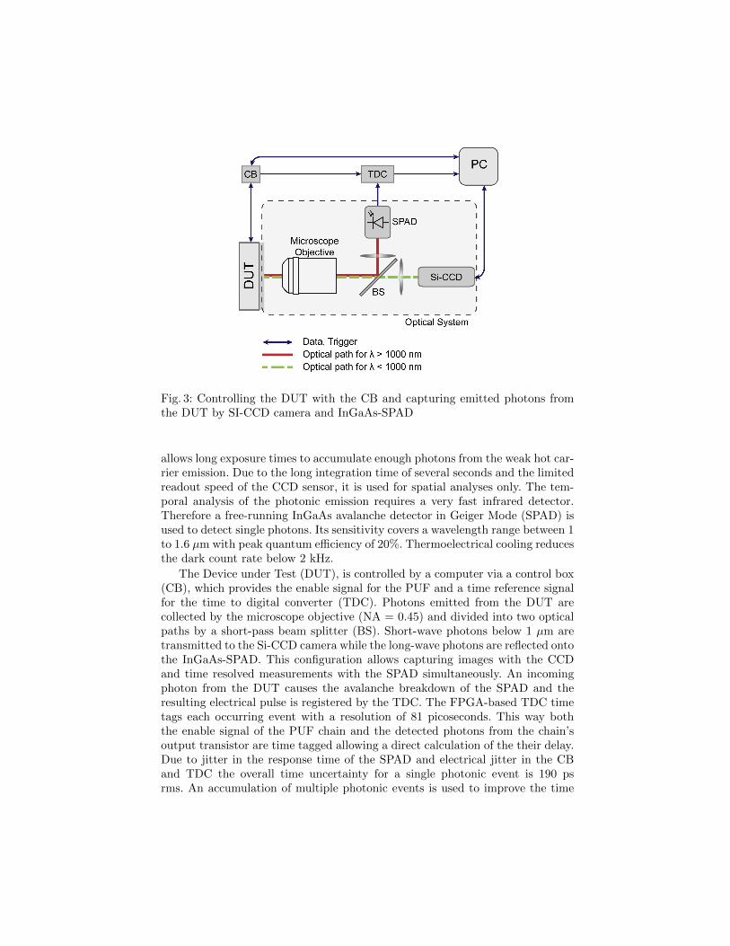
Fig. 3: Controlling the DUT with the CB and capturing emitted photons fromthe DUT by SI-CCD camera and InGaAs-SPAD
allows long exposure times to accumulate enough photons from the weak hot car-rier emission. Due to the long integration time of several seconds and the limitedreadout speed of the CCD sensor, it is used for spatial analyses only. The tem-poral analysis of the photonic emission requires a very fast infrared detector.Therefore a free-running InGaAs avalanche detector in Geiger Mode (SPAD) isused to detect single photons. Its sensitivity covers a wavelength range between 1to 1.6 µm with peak quantum efficiency of 20%. Thermoelectrical cooling reducesthe dark count rate below 2 kHz.
The Device under Test (DUT), is controlled by a computer via a control box(CB), which provides the enable signal for the PUF and a time reference signalfor the time to digital converter (TDC). Photons emitted from the DUT arecollected by the microscope objective (NA = 0.45) and divided into two opticalpaths by a short-pass beam splitter (BS). Short-wave photons below 1 µm aretransmitted to the Si-CCD camera while the long-wave photons are reflected ontothe InGaAs-SPAD. This configuration allows capturing images with the CCDand time resolved measurements with the SPAD simultaneously. An incomingphoton from the DUT causes the avalanche breakdown of the SPAD and theresulting electrical pulse is registered by the TDC. The FPGA-based TDC timetags each occurring event with a resolution of 81 picoseconds. This way boththe enable signal of the PUF chain and the detected photons from the chain’soutput transistor are time tagged allowing a direct calculation of the their delay.Due to jitter in the response time of the SPAD and electrical jitter in the CBand TDC the overall time uncertainty for a single photonic event is 190 psrms. An accumulation of multiple photonic events is used to improve the time
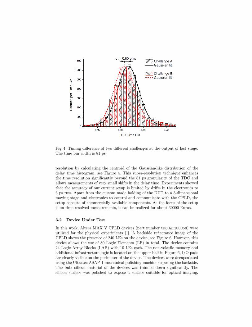
Fig. 4: Timing difference of two different challenges at the output of last stage.The time bin width is 81 ps
resolution by calculating the centroid of the Gaussian-like distribution of thedelay time histogram, see Figure 4. This super-resolution technique enhancesthe time resolution significantly beyond the 81 ps granularity of the TDC andallows measurements of very small shifts in the delay time. Experiments showedthat the accuracy of our current setup is limited by drifts in the electronics to6 ps rms. Apart from the custom made holding of the DUT to a 3-dimensionalmoving stage and electronics to control and communicate with the CPLD, thesetup consists of commercially available components. As the focus of the setupis on time resolved measurements, it can be realized for about 30000 Euros.
3.2 Device Under Test
In this work, Altera MAX V CPLD devices (part number 5M80ZT100C5N) wereutilized for the physical experiments [1]. A backside reflectance image of theCPLD shows the presence of 240 LEs on the device, see Figure 6. However, thisdevice allows the use of 80 Logic Elements (LE) in total. The device contains24 Logic Array Blocks (LAB) with 10 LEs each. The non-volatile memory andadditional infrastructure logic is located on the upper half in Figure 6, I/O padsare clearly visible on the perimeter of the device. The devices were decapsulatedusing the Ultratec ASAP-1 mechanical polishing machine exposing the backside.The bulk silicon material of the devices was thinned down significantly. Thesilicon surface was polished to expose a surface suitable for optical imaging.
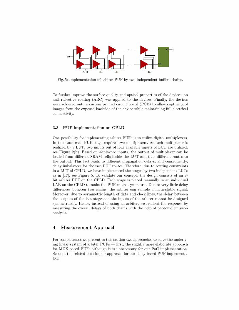
Fig. 5: Implementation of arbiter PUF by two independent buffers chains.
To further improve the surface quality and optical properties of the devices, ananti reflective coating (ARC) was applied to the devices. Finally, the deviceswere soldered onto a custom printed circuit board (PCB) to allow capturing ofimages from the exposed backside of the device while maintaining full electricalconnectivity.
3.3 PUF implementation on CPLD
One possibility for implementing arbiter PUFs is to utilize digital multiplexers.In this case, each PUF stage requires two multiplexers. As each multiplexer isrealized by a LUT, two inputs out of four available inputs of LUT are utilized,see Figure 2(b). Based on don’t-care inputs, the output of multiplexer can beloaded from different SRAM cells inside the LUT and take different routes tothe output. This fact leads to different propagation delays, and consequently,delay imbalances for the two PUF routes. Therefore, due to routing constraintsin a LUT of CPLD, we have implemented the stages by two independent LUTsas in [17], see Figure 5. To validate our concept, the design consists of an 8-bit arbiter PUF on the CPLD. Each stage is placed manually in an individualLAB on the CPLD to make the PUF chains symmetric. Due to very little delaydifferences between two chains, the arbiter can sample a meta-stable signal.Moreover, due to asymmetric length of data and clock lines, the delay betweenthe outputs of the last stage and the inputs of the arbiter cannot be designedsymmetrically. Hence, instead of using an arbiter, we readout the response bymeasuring the overall delays of both chains with the help of photonic emissionanalysis.
4 Measurement Approach
For completeness we present in this section two approaches to solve the underly-ing linear system of arbiter PUFs — first, the slightly more elaborate approachfor MUX-based PUFs although it is unnecessary for our PoC implementation.Second, the related but simpler approach for our delay-based PUF implementa-tion.
4.1 Optimized Measurement for ordinary MUX-based PUFCharacterization
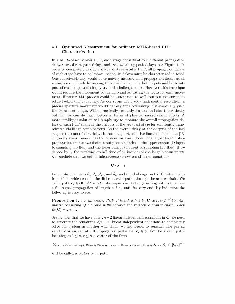
In a MUX-based arbiter PUF, each stage consists of four different propagationdelays: two direct path delays and two switching path delays, see Figure 1. Inorder to completely characterize an n-stage arbiter PUF, all propagation delaysof each stage have to be known, hence, 4n delays must be characterized in total.One conceivable way would be to naively measure all 4 propagation delays at alln stages individually by moving the optical setup over both inputs and both out-puts of each stage, and simply try both challenge states. However, this techniquewould require the movement of the chip and adjusting the focus for each move-ment. However, this process could be automated as well, but our measurementsetup lacked this capability. As our setup has a very high spatial resolution, aprecise aperture movement would be very time consuming, but eventually yieldthe 4n arbiter delays. While practically certainly feasible and also theoreticallyoptimal, we can do much better in terms of physical measurement efforts. Amore intelligent solution will simply try to measure the overall propagation de-lays of each PUF chain at the outputs of the very last stage for sufficiently manyselected challenge combinations. As the overall delay at the outputs of the laststage is the sum of all n delays in each stage, cf. additive linear model due to [13,13], every measurement has to consider for every chosen challenge the completepropagation time of two distinct but possible paths — the upper output (D inputto sampling flip-flop) and the lower output (C input to sampling flip-flop). If wedenote by ri the resulting overall time of an individual challenge measurement,we conclude that we get an inhomogeneous system of linear equations
C · δ = r
for our 4n unknowns δia , δib , δic , and δid and the challenge matrix C with entriesfrom {0, 1} which encode the different valid paths through the arbiter chain. Wecall a path ci ∈ {0,1}4n valid if its respective challenge setting within C allowsa full signal propagation of length n, i.e., until its very end. By induction thefollowing is easy to see.
Proposition 1. For an arbiter PUF of length n ≥ 1 let C be the (2n+1)× (4n)matrix consisting of all valid paths through the respective arbiter chain. Thenrk(C) = 2n+ 2.
Seeing now that we have only 2n+2 linear independent equations in C, we needto generate the remaining 2(n − 1) linear independent equations to completelysolve our system in another way. Thus, we are forced to consider also partialvalid paths instead of full propagation paths. Let ci ∈ {0,1}4n be a valid path;for integers 1 ≤ u, v ≤ n a vector of the form
(0, . . . , 0, c4u, c4u+1, c4u+2, c4u+3, . . . , c4v, c4v+1, c4v+2, c4v+3, 0, . . . , 0) ∈ {0,1}4n
will be called a partial valid path.
Note 1. For a partial valid path we will measure its signal time only from theinputs of arbiter stage u until its output at stage v and deliberately denote thispartial time simply also by ri.
Including such partial measurements ri (i.e. including measurements within thearbiter chain) and their corresponding paths ci we also get by induction.
Proposition 2. For an arbiter PUF of length n ≥ 1 and its 2n+ 2 valid paths(corresponding to the linear independent row vectors) there exist 2(n− 1) appro-priate partial valid paths such that their combined challenge matrix C has fullrank 4n.
This Proposition implies that we only need 2(n−1) partial measurements whichwe classify with respect to u and v into three classes:
1. u = 1 and 1 ≤ v < n: Measurement begins at the inputs of the first stageand ends in the middle of the chain.
2. 1 < u, v < n: Measurement starts at some inputs in the middle of the chainand also ends in the middle of the chain.
3. 1 < u ≤ n and v = n: Measurement starts at the inputs in the middle of thearbiter chain and and ends after the last stage.
In order to keep the previously discussed physical measurement efforts minimal,it is therefore obvious to generate the missing linear independent equations outof group 1 or 3 — dependent on varying setup advantages. This completes ourdescription of an optimized measurement for a classical MUX-based PUF withn stages.
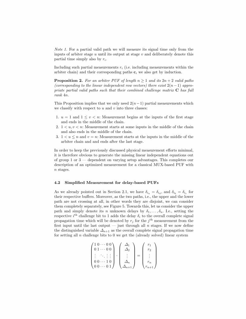
4.2 Simplified Measurement for delay-based PUFs
As we already pointed out in Section 2.1, we have δia = δid , and δib = δic fortheir respective buffers. Moreover, as the two paths, i.e., the upper and the lowerpath are not crossing at all, in other words they are disjoint, we can considerthem completely separately, see Figure 5. Towards this, let us consider the upperpath and simply denote its n unknown delays by δ1, . . . , δn. I.e., setting therespective ith challenge bit to 1 adds the delay δi to the overall complete signalpropagation time which will be denoted by rj for the jth measurement from thefirst input until the last output — just through all n stages. If we now definethe distinguished variable ∆n+1 as the overall complete signal propagation timefor setting all n challenge bits to 0 we get the (already solved) linear system
1 0 · · · 0 00 1 · · · 0 0...
. . ....
...0 0 · · · 1 00 0 · · · 0 1
·
∆1
∆2
...∆n
∆n+1
=
r1r2...rnrn+1
for which we simply require the measurements ri, i = 1, . . . , n + 1. The lowerpath can be handled in an analog way, say C′ ·∆′ = r′. Moreover, using the unitvectors ei ∈ {0, 1}n+1, i = 1, . . . , n+ 1, we find that we get from
ei ·∆− en+1 ·∆ = ri − rn+1, and
ei ·∆′ − en+1 ·∆′ = r′i − r′n+1
the two individual buffer delays δi and δ′i of stage i incurred by setting theith challenge bit to 1. We thus conclude that we need only 2n + 2 “full path”measurements to completely characterize a delay-based PUF with n stages.
5 Results
We have chosen the challenge 00000000 as the reference challenge for our mea-surements. In order to measure the effect of each challenge bit, we have tried thechallenge combinations with hamming distance one to see the effect of each chal-lenge bit individually. The enable signal was switched with a frequency of 4 MHzand the chip was supplied with 2.2 V. The optical emission of the PUF circuitreveals the position of each stage, see Figure 6. Moreover, the inputs and out-put of each stage for measurement can also be found on this emission image. Incase of controlled PUFs, where no electrical access to challenges is available [8],comparing the optical emission of the PUF stages can also reveal the state ofindividual challenge bits. By changing each challenge bit, the emission patternof each LE is changed, and therefore, the challenge can be read without any elec-trical access to it, see Figure 7. Therefore, the equations provided in Section 4can still be used to characterize the PUF by finding challenges with hammingdistance one from each other. We repeated the measurement 50 million cyclesto capture enough number of photons for analysis. The reference challenge alsohas been measured multiple times during our experiments to compare the con-sistency of measurements. The measurement results of 8 challenge combinationscompared to the reference challenge can be found in Figure 8. Positive timingdifference means that the delay is decreased in comparison to reference challengeand vice versa. It can be seen that flipping the challenge bit from 0 to 1, makesin most cases both upper and lower chains faster. Moreover, the timing differ-ences between both chains can also be found in the table. Based on the overalldelay difference of two chains, the response can be predicted. In this case, if thetiming difference between two chains is positive, the response is 1, otherwise theresponse is 0.
According to the measured values, we can predict the behavior of both chainsfor all other challenge combinations based on the linear additive model of thearbiter PUF. To prove the applicability of this model, we predicted theoreticallythe overall delay of both chains for a set of arbitrary challenge combinations,and then measured the timings in practice. For instance, the calculated timingdifference between both chains for the challenge 00000111 is the sum of measureddifferences of challenges 00000001, 00000010 and 00000100, which is 195 ps.
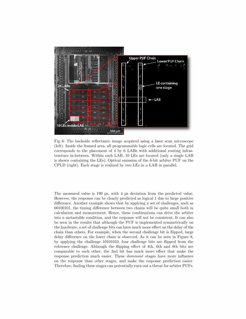
Fig. 6: The backside reflectance image acquired using a laser scan microscope(left). Inside the framed area, all programmable logic cells are located. The gridcorresponds to the placement of 4 by 6 LABs with additional routing infras-tructure in-between. Within each LAB, 10 LEs are located (only a single LABis shown containing the LEs). Optical emission of the 8-bit arbiter PUF on theCPLD (right). Each stage is realized by two LEs in a LAB in parallel.
The measured value is 199 ps, with 4 ps deviation from the predicted value.However, the response can be clearly predicted as logical 1 due to large positivedifference. Another example shows that by applying a set of challenges, such as00100101, the timing difference between two chains will be quite small both incalculation and measurement. Hence, these combinations can drive the arbiterinto a metastable condition, and the response will not be consistent. It can alsobe seen in the results that although the PUF is implemented symmetrically onthe hardware, a set of challenge bits can have much more effect on the delay of thechain than others. For example, when the second challenge bit is flipped, largedelay difference on the lower chain is observed. As it can be seen in Figure 8,by applying the challenge 10101010, four challenge bits are flipped from thereference challenge. Although the flipping effect of 4th, 6th and 8th bits arecomparable to each other, the 2nd bit has much more effect that make theresponse prediction much easier. These dominant stages have more influenceon the response than other stages, and make the response prediction easier.Therefore, finding these stages can potentially turn out a threat for arbiter PUFs.
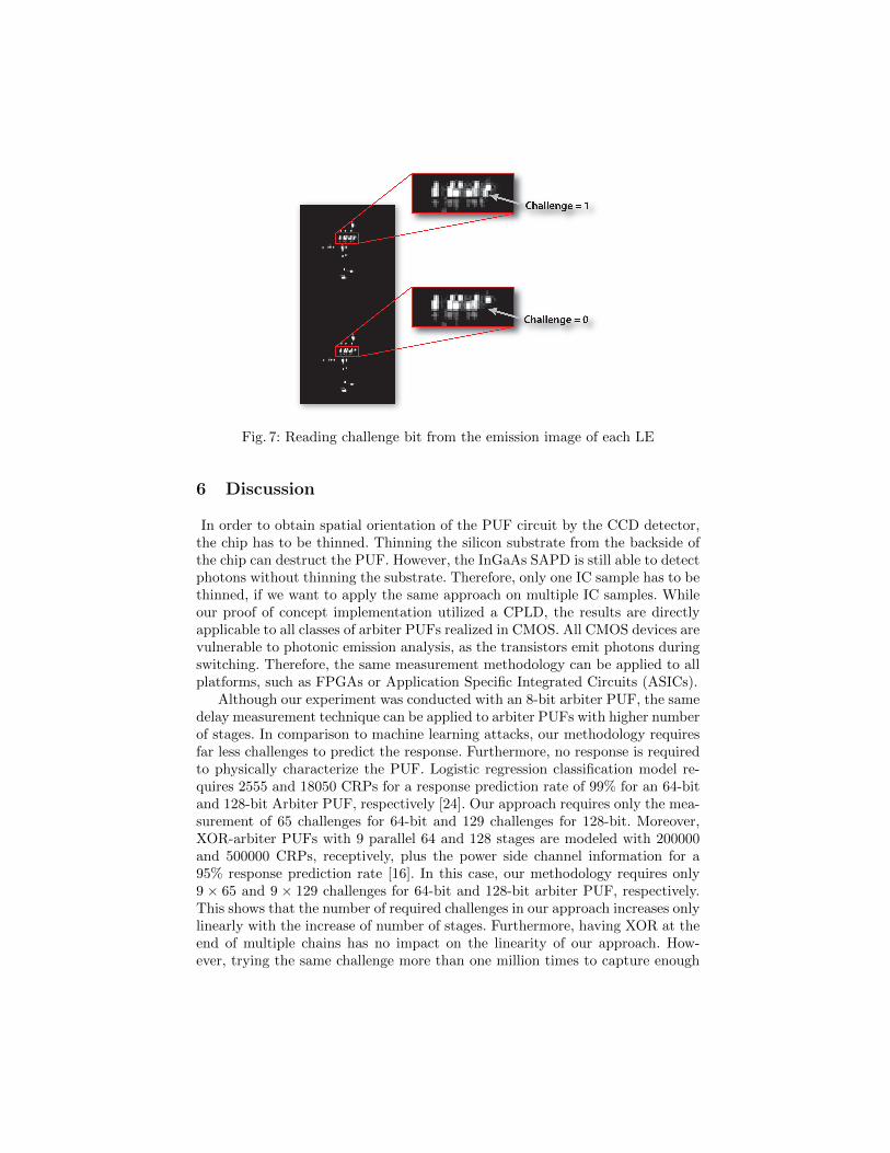
Fig. 7: Reading challenge bit from the emission image of each LE
6 Discussion
In order to obtain spatial orientation of the PUF circuit by the CCD detector,the chip has to be thinned. Thinning the silicon substrate from the backside ofthe chip can destruct the PUF. However, the InGaAs SAPD is still able to detectphotons without thinning the substrate. Therefore, only one IC sample has to bethinned, if we want to apply the same approach on multiple IC samples. Whileour proof of concept implementation utilized a CPLD, the results are directlyapplicable to all classes of arbiter PUFs realized in CMOS. All CMOS devices arevulnerable to photonic emission analysis, as the transistors emit photons duringswitching. Therefore, the same measurement methodology can be applied to allplatforms, such as FPGAs or Application Specific Integrated Circuits (ASICs).
Although our experiment was conducted with an 8-bit arbiter PUF, the samedelay measurement technique can be applied to arbiter PUFs with higher numberof stages. In comparison to machine learning attacks, our methodology requiresfar less challenges to predict the response. Furthermore, no response is requiredto physically characterize the PUF. Logistic regression classification model re-quires 2555 and 18050 CRPs for a response prediction rate of 99% for an 64-bitand 128-bit Arbiter PUF, respectively [24]. Our approach requires only the mea-surement of 65 challenges for 64-bit and 129 challenges for 128-bit. Moreover,XOR-arbiter PUFs with 9 parallel 64 and 128 stages are modeled with 200000and 500000 CRPs, receptively, plus the power side channel information for a95% response prediction rate [16]. In this case, our methodology requires only9 × 65 and 9 × 129 challenges for 64-bit and 128-bit arbiter PUF, respectively.This shows that the number of required challenges in our approach increases onlylinearly with the increase of number of stages. Furthermore, having XOR at theend of multiple chains has no impact on the linearity of our approach. How-ever, trying the same challenge more than one million times to capture enough
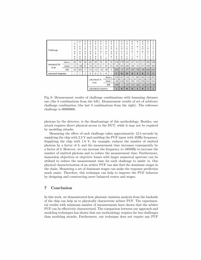
Fig. 8: Measurement results of challenge combinations with hamming distanceone (the 8 combinations from the left). Measurement results of set of arbitrarychallenge combination (the last 8 combinations from the right). The referencechallenge is 00000000.
photons by the detector, is the disadvantage of this methodology. Besides, ourattack requires direct physical access to the DUT, while it may not be requiredby modeling attacks.
Measuring the effect of each challenge takes approximately 12.5 seconds bysupplying the chip with 2.2 V and enabling the PUF input with 4MHz frequency.Supplying the chip with 1.8 V, for example, reduces the number of emittedphotons by a factor of 3, and the measurement time increases consequently bya factor of 3. However, we can increase the frequency to 100MHz to increase thenumber of emitted photons and to reduce the measurement time. Furthermore,immersion objectives or objective lenses with larger numerical aperture can beutilized to reduce the measurement time for each challenge to under 1s. Ourphysical characterization of an arbiter PUF can also find the dominant stages inthe chain. Measuring a set of dominant stages can make the response predictionmuch easier. Therefore, this technique can help to improve the PUF behaviorby designing and constructing more balanced routes and stages.
7 Conclusion
In this work, we demonstrated how photonic emission analysis from the backsideof the chip can help us to physically characterize arbiter PUF. The experimen-tal results with minimum number of measurements have shown that the arbiterPUF can be effectively characterized. The comparison between our approach andmodeling techniques has shown that our methodology requires far less challengesthan modeling attacks. Furthermore, our technique does not require any PUF
response. Although we carried out our experiments on a CPLD PUF implementa-tion, the same methodology can be applied to other hardware implementations.As a result, it is revealed that the timing-based PUFs, specifically arbiter PUFs,are vulnerable to photonic emission analysis.
Acknowledgements. The authors would like to acknowledge the support of theGerman Federal Ministry of Education and Research in the project PhotonFXand the Helmholtz Research School on Security Technologies.
References
1. Altera: MAX V Device Handbook. Altera Corporation, San Jose (2011)2. Altera: Quartus II Web Edition Software (2013), http://www.altera.com/
products/software/quartus-ii/web-edition/qts-we-index.html
3. Armknecht, F., Maes, R., Sadeghi, A., Standaert, O.X., Wachsmann, C.: A For-malization of the Security Features of Physical Functions. In: Security and Privacy(SP), 2011 IEEE Symposium on. pp. 397–412. IEEE (2011)
4. Boit, C.: Fundamentals of Photon Emission (PEM) in Silicon – Electrolumines-cence for Analysis of Electronic Circuit and Device Functionality. In: Microelec-tronics Failure Analysis: Desk Reference. p. 356 ff. ASM International (2004)
5. Delvaux, J., Verbauwhede, I.: Fault Injection Modeling Attacks on 65nm Ar-biter and RO Sum Pufs via Environmental changes. Tech. rep., Cryptology ePrintArchive: Report 2013/619, 2013, https://eprint. iacr. org/2013/619 (2013)
6. Delvaux, J., Verbauwhede, I.: Side Channel Modeling Attacks on 65nm ArbiterPUFs Exploiting CMOS Device Noise. In: Hardware-Oriented Security and Trust(HOST), 2013 IEEE International Symposium on. pp. 137–142. IEEE (2013)
7. Ferrigno, J., Hlavac, M.: When AES Blinks: Introducing Optical Side Chan-nel. Information Security, IET 2(3), 94 –98 (2008), http://dx.doi.org/10.1049/iet-ifs:20080038
8. Gassend, B., Clarke, D., Van Dijk, M., Devadas, S.: Controlled Physical Ran-dom Functions. In: Computer Security Applications Conference, 2002. Proceed-ings. 18th Annual. pp. 149–160. IEEE (2002)
9. Gassend, B., Clarke, D., Van Dijk, M., Devadas, S.: Silicon Physical Random Func-tions. In: Proceedings of the 9th ACM conference on Computer and communica-tions security. pp. 148–160. ACM (2002)
10. Helfmeier, C., Boit, C., Nedospasov, D., Seifert, J.P.: Cloning Physically Unclon-able Functions. In: Hardware-Oriented Security and Trust (HOST), 2013 IEEEInternational Symposium on. pp. 1–6. IEEE (2013)
11. Kramer, J., Nedospasov, D., Schlosser, A., Seifert, J.P.: Differential Photonic Emis-sion Analysis. In: Constructive Side-Channel Analysis and Secure Design, pp. 1–16.Springer (2013)
12. Lee, J.W., Lim, D., Gassend, B., Suh, G.E., Van Dijk, M., Devadas, S.: A Techniqueto Build a Secret Key in Integrated Circuits for Identification and AuthenticationApplications. In: VLSI Circuits, 2004. Digest of Technical Papers. 2004 Symposiumon. pp. 176–179. IEEE (2004)
13. Lim, D., Lee, J.W., Gassend, B., Suh, G.E., Van Dijk, M., Devadas, S.: Extract-ing Secret Keys from Integrated Circuits. Very Large Scale Integration (VLSI)Systems, IEEE Transactions on 13(10), 1200–1205 (2005)
14. Maes, R., Van Herrewege, A., Verbauwhede, I.: PUFKY: A Fully Functional Puf-based Cryptographic Key Generator. In: Cryptographic Hardware and EmbeddedSystems–CHES 2012, pp. 302–319. Springer (2012)
15. Maes, R., Verbauwhede, I.: Physically Unclonable Functions: A Study on the Stateof the Art and Future Research Directions. In: Towards Hardware-Intrinsic Secu-rity, pp. 3–37. Springer (2010)
16. Mahmoud, A., Ruhrmair, U., Majzoobi, M., Koushanfar, F.: Combined Modelingand Side Channel Attacks on Strong PUFs. Tech. rep., Cryptology ePrint Archive:Report 2013/632, 2013, https://eprint. iacr. org/2013/632 (2013)
17. Majzoobi, M., Koushanfar, F., Devadas, S.: FPGA PUF using Programmable De-lay Lines. In: Information Forensics and Security (WIFS), 2010 IEEE InternationalWorkshop on. pp. 1–6. IEEE (2010)
18. Merli, D., Schuster, D., Stumpf, F., Sigl, G.: Semi-invasive EM Attack on FPGARO PUFs and Countermeasures. In: Proceedings of the Workshop on EmbeddedSystems Security. p. 2. ACM (2011)
19. Nedospasov, D., Schlosser, A., Seifert, J.P., Orlic, S.: Functional Integrated CircuitAnalysis. Hardware-Oriented Security and Trust (HOST), 2012 IEEE InternationalSymposium on pp. 102–107 (2012)
20. Nedospasov, D., Seifert, J.P., Helfmeier, C., Boit, C.: Invasive PUF Analysis. In:Fault Diagnosis and Tolerance in Cryptography (FDTC), 2013 Workshop on. pp.30–38. IEEE (2013)
21. Oztiirk, E., Hammouri, G., Sunar, B.: Towards Robust Low Cost Authenticationfor Pervasive Devices. In: Pervasive Computing and Communications, 2008. Per-Com 2008. Sixth Annual IEEE International Conference on. pp. 170–178. IEEE(2008)
22. Parusinski, M., Shariati, S., Kamel, D., Xavier-Standaert, F.: Strong PUFs andtheir (Physical) Unpredictability: A Case Study with Power PUFs. In: Proceedingsof the Workshop on Embedded Systems Security. p. 5. ACM (2013)
23. Rankl, W., Effing, W.: Smart Card Handbook. Wiley, fourth edn. (2010)
24. Ruhrmair, U., Sehnke, F., Solter, J., Dror, G., Devadas, S., Schmidhuber, J.: Mod-eling Attacks on Physical Unclonable Functions. In: Proceedings of the 17th ACMconference on Computer and communications security. pp. 237–249. ACM (2010)
25. Ruhrmair, U., Solter, J., Sehnke, F.: On the Foundations of Physical UnclonableFunctions. IACR Cryptology ePrint Archive 2009, 277 (2009)
26. Sadeghi, A.R., Visconti, I., Wachsmann, C.: Enhancing RFID Security and Privacyby Physically Unclonable Functions. Springer (2010)
27. Schlosser, A., Dietz, E., Frohmann, S., Orlic, S.: Highly Resolved Spatial and Tem-poral Photoemission Analysis of Integrated Circuits. Measurement Science andTechnology 24(3), 035102 (2013)
28. Schlosser, A., Nedospasov, D., Kramer, J., Orlic, S., Seifert, J.P.: Simple PhotonicEmission Analysis of AES. In: Cryptographic Hardware and Embedded Systems–CHES 2012, pp. 41–57. Springer (2012)
29. Skoric, B., Tuyls, P., Ophey, W.: Robust Key Extraction from Physical UncloneableFunctions. In: Applied Cryptography and Network Security. pp. 407–422. Springer(2005)
30. Skorobogatov, S.: Optical Fault Masking Attacks. In: Fault Diagnosis and Toler-ance in Cryptography (FDTC), 2010 Workshop on. pp. 23–29. IEEE (2010)
31. Skorobogatov, S.P., Anderson, R.J.: Optical Fault Induction Attacks. In: Crypto-graphic Hardware and Embedded Systems-CHES 2002, pp. 2–12. Springer (2003)

32. Suh, G.E., Devadas, S.: Physical Unclonable Functions for Device Authenticationand Secret Key Generation. In: Proceedings of the 44th annual Design AutomationConference. pp. 9–14. ACM (2007)
33. Tuyls, P., Batina, L.: RFID-tags for Anti-Counterfeiting. In: Topics in Cryptology–CT-RSA 2006, pp. 115–131. Springer (2006)